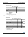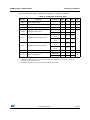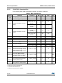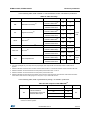
1
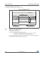
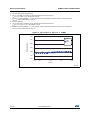
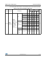
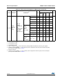
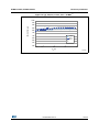
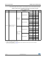
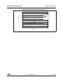
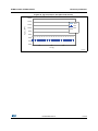
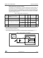
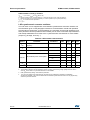
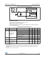
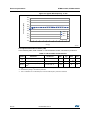
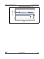
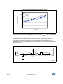
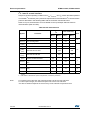
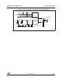
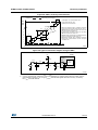
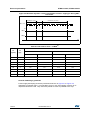
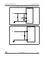
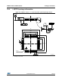
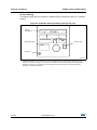
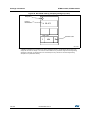
STM8L151x4/6, STM8L152x4/6 Electrical parameters Figure 38. ADC1 accuracy characteristics V V [1LSBIDEAL = REF+ (or DDA depending on package)] 4096 4096 EG (1) Example of an actual transfer curve (2) The ideal transfer curve (3) End point correlation line 4095 4094 4093 (2) ET 7 (1) 6 5 4 ET=Total Unadjusted Error: maximum deviation between the actual and the ideal transfer curves. EO=Offset Error: deviation between the first actual transition and the first ideal one. EG=Gain Error: deviation between the last ideal transition and the last actual one. ED=Differential Linearity Error: maximum deviation between actual steps and the ideal one. EL=Integral Linearity Error: maximum deviation between any actual transition and the end point correlation line. (3) EO EL 3 ED 2 1 LSBIDEAL 1 0 1 VSSA 2 3 4 5 6 7 4093 4094 4095 4096 VDDA ai14395b Figure 39. Typical connection diagram using the ADC 670 9'' 6DPSOHDQGKROG$'& FRQYHUWHU 97 9 5$,1 9$,1 5$'& $,1[ &SDUDVLWLF 97 9 ELW FRQYHUWHU &$'& , / Q$ DLI 1. Refer to Table 53 for the values of RAIN and CADC. 2. Cparasitic represents the capacitance of the PCB (dependent on soldering and PCB layout quality) plus the pad capacitance (roughly 7 pF). A high Cparasitic value will downgrade conversion accuracy. To remedy this, fADC should be reduced. DocID15962 Rev 14 111/142 115