1
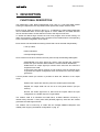
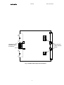
Technical
Information
Manual
29 January 1993
MOD. V495
DUAL PROGRAMMABLE
LOGIC UNIT
CAEN will repair or replace any product within the guarantee period if the Guarantor declares that
the product is defective due to workmanship or materials and has not been caused by mishandling,
negligence on behalf of the User, accident or any abnormal conditions or operations.
CAEN declines all responsibility for damages or injuries
caused by an improper use of the Modules due to
negligence on behalf of the User. It is strongly
recommended to read thoroughly the CAEN User's
Manual before any kind of operation.
CAEN reserves the right to change partially or entirely the contents of this Manual at any time and
without giving any notice.
TABLE OF CONTENTS
1.
DESCRIPTION .....................................................................................................................1
FUNCTIONAL DESCRIPTION........................................................................................1
2.
SPECIFICATIONS................................................................................................................3
PACKAGING ...................................................................................................................3
EXTERNAL COMPONENTS...........................................................................................3
INTERNAL COMPONENTS............................................................................................4
POWER REQUIREMENTS.............................................................................................4
CHARACTERISTICS OF THE SIGNALS........................................................................4
3.
OPERATING MODES ..........................................................................................................8
LOOK-UP TABLE............................................................................................................8
PATTERN GENERATOR................................................................................................8
INPUT/OUTPUT REGISTER ..........................................................................................9
FRONT PANEL SIGNALS...............................................................................................9
MODULE CONFIGURATION..........................................................................................10
4.
VME INTERFACE.................................................................................................................11
ADDRESSING CAPABILITY...........................................................................................11
DATA TRANSFER CAPABILITY.....................................................................................11
MODULE IDENTIFIER WORDS .....................................................................................13
CONFIGURATION REGISTER.......................................................................................13
ADDRESS REGISTER....................................................................................................14
RAM ................................................................................................................................15
INPUT STROBE..............................................................................................................15
OUTPUT/INPUT REGISTER ..........................................................................................16
5.
REFERENCES .....................................................................................................................17
29/01/93
V495 User Manual
1. DESCRIPTION
FUNCTIONAL DESCRIPTION
The CAEN Mod. V495, Dual Programmable Logic Unit, is a 1-unit wide VME module
housing 2 independent Look-Up Tables with 8 Input and 8 Output channels each.
Each Look-Up Table, as shown in the Fig 1.1, is realized by a 256 locations RAM that
can be addressed either via the input signals or via the VME bus; the RAM data bus
can be read and written via the VME bus or fed to the output connectors.
To obtain the desired logic function the user must program each section writing, via
VME, the necessary configuration of the outputs into the RAM locations corresponding
to the correlated configuration of the Inputs.
Each section has three different working modes that can be selected independently:
Look-Up Table;
Pattern Generator
8 bit Input/Output Register
Some coaxial connectors housed in the front panel accept the following NIM signals:
STB:STROBE one input signal per section sent through this connector
latches the input channels status inside the relevant INPUT REGISTER;
SYNC:SYNC an output signal per section which becomes true when the
outputs become valid;
CLK:CLOCK input signal common to both sections used as external clock
to generate the output configuration when the sections are used as pattern
generators.
A three position switch per section is provided to allow the selection of the output
mode:
Strobed: the outputs are valid only when the strobe signal is asserted;
Shaped: the output width can be set via a front panel trimmer (one per
section);
Normal: the strobe signal has no effect and the outputs follow the input
configuration; the SYNC output is not generated.
The module V495 is an A24/A32 D16 VME slave; its Base address is fixed by 6
internal rotary switches. A front panel LED (DTACK) lights up each time the module
generates the VME signal DTACK.
The module can be used only in crates with the V430[2] VMEbus backplane and
related power supply (see Module configuration on pag. 9)
1
Fig. 1.1: Mod. V495 block diagram
2
T rigger
E xt. ST R O B E
B IT 6 (7)
S
H
A
P
E
R
V cc
B IT 10
S
E
Q
U
E
N
C
E
R
E xt. Trimmer
S Y S CLO C K
E xt. Clock
8
8
R
E
G
I
S
T
E
R
8
V M E A D D R E SS B U S 0..7
A
D
D
R
E
S
S
V M E D A T A B US 0..7
T o the other section
I
N
P
U
T
S
C O NF IG U R A TIO N R E G IS T E R
B IT 0 (1)
8
V cc
V cc
8
STROBED
S H A PE D
N O RM A L
B IT 5 (4)
C
O
M
P.
B IT 7
E xt. Selector
B IT 2 (3)
V M E D A T A B US 0..7
265 X 8
RAM
8
B IT 8 (9)
8
S
H
A
P
E
R
T rigger
E nable
O
U
T
P
U
T
S
E xt. SY N C
29/01/93
V495 User Manual
29/01/93
V495 User Manual
2. SPECIFICATIONS
PACKAGING
1-unit wide VME unit.
EXTERNAL COMPONENTS
CONNECTORS
- No.2, "IN 0..7" A, "IN 0..7" B, 16 pin lead flat cable connector, 110Ω impedance; for
the 8 input channels of each section.
- No.2, "STB", LEMO 00 type, delivered in high impedance configuration; 50Ω
terminations selectable via internal jumpers, for the Strobe input signals (one for each
section).
- No.2, "SYNC", LEMO 00 type, 50Ω impedance;for the Synchronization output signals
(one for each section).
- No.1, "CLK", LEMO 00 type 50Ω impedance;for the external Clock input.
LEDs
- No.1, "DTACK", green, VME Selected; it lights up during a VME access.
SWITCHES
- No.2, "STB...NORM...SHP":three position switch (one per section):
STB to select the Strobed output mode;
SHP to select the Shaped output mode;
NORM to select the Normal output mode.
TRIMMERS
- No.2, "WDT" (one per section): to set the output width when the Shaped mode is
selected.
3
29/01/93
V495 User Manual
INTERNAL COMPONENTS
(refer to fig.2.2 and Appendix C - components location)
JUMPERS
- No.2,"JP3" and "JP4"; for the insertion of the 50• terminations of the strobe signals.
SWITCHES
- No.6, rotary switches for the module VME Base address selection.
POWER REQUIREMENTS
+5V
1.1 A
-2V
800 mA
-5V
2.6 A
CHARACTERISTICS OF THE SIGNALS
- INPUT CHANNELS: std. differential ECL level, 110 Ω impedance;
NORMAL output mode:
max. frequency: 200 MHz , min. width 2.5 ns ;
Input/Output delay• 8 ns.
STROBED and SHAPED output mode:
Input Set-up time: 0 ns;
Input Hold time : 4.5 ns.
N.B. The above mentioned times are referred to the STROBE
signal leading edge.
- STB:
std. NIM level, high impedance;
min. width 2.5 ns;
max frequency : 180 MHz;
delay STROBE/VALID OUTPUT: 13 ns;
double pulse resolution:automatically limited by the Input Hold
time.
- SYNC:
std. NIM level, 50•; min. width: 3 ns
delay STROBE/SYNC : 11 ns.
N.B. The outputs are valid at the SYNC trailing edge
- CLK:
std. NIM level, high impedance; max. frequency •50 MHz ( Free
running with programmed stop);
min. width: 10 ns.
4
29/01/93
- OUTPUT CHANNELS: std. differential ECL level, 110 Ω impedance;
Output width:
SHAPED output mode from 12 ns to 60 ns;
STROBED output mode equal to the STROBE width.
5
V495 User Manual
29/01/93
M o d. V 4 9 5
WDT
SHP
STB
NO RM
+ -
+ -
IN
OUT
7
A
0
STB
A
SYNC
D
T
A
C
K
C
L
K
SYNC
B
STB
+ -
+ -
IN
OUT
7
A
0
NO RM
STB
SHP
WDT
D U AL P R O G R .
L O G IC U N IT
Fig. 2.1: Mod. V495 Front panel
6
V495 User Manual
29/01/93
V495 User Manual
JP 3
Jumpers for 50 Ω
STROBE signals
terminations
Rotary switches
for Base Address
selection
JP 4
Fig. 2.2: Mod. V495 components locations
7
29/01/93
V495 User Manual
3. OPERATING MODES
The output of the single unit Independently from the selected operating mode can be
selected to be valid in one of the following output modes:
STROBED
the leading edge of the external or internally software generated
STROBE signal freezes the inputs' configuration of the section and
the relevant configuration of the outputs is then placed on the output
connector; the output drivers are always in reset mode except during
the STROBE signal. If the input configuration changes during the
STROBE interval, the variations do not affect the output configuration
freezed at the leading edge time1. The output is then valid ONLY
during the STROBE signal width.
SHAPED
the unit works as above except that the output width is fixed by via a
front panel trimmer per section in a range that can vary from 12 ns to
65 ns.
NORMAL
the output varies all the time according to the input configuration.
LOOK-UP TABLE
The module V495 houses 2 independent sections, labelled A and B, with 8 inputs and
8 outputs.
Before using the unit, the 256 RAM locations of each section must be programmed to
keep the desired output bit configuration according to the logic function which has to be
realized. The front panel three position switch of each section has to be set according
to the desired output mode.
PATTERN GENERATOR
The module can be a two section PATTERN GENERATOR. The input connector of
each section is then replaced by an ADDRESS REGISTER which sequentially drives
the RAM address bus starting from the first programmable via VME.
The output configurations are placed on the output connectors at the rate fixed by the
VME system clock or by an external clock fed to the relevant CLK input connector.
The operations of the V495 as PATTERN GENERATOR are fully software
programmable; via VME it is possible:
to fill the RAM locations with the desired configurations;
to program the RAM starting address for the sequence of the patterns;
to select the internal VME system clock, 16 MHz, or the external clock source;
to select between two different subsets of operations:
1Due to internal delays the inputs are freezed after 5 ns from the STROBE leading
edge; the outputs are valid after 13 ns from the the same leading edge and valid for a
time equal to the STROBE width.In any case the output validity is signalled by the
SYNC trailing edge.
8
29/01/93
V495 User Manual
Free running: after the programming of the starting address the pattern
generation start is given via VME. The section scans all the RAM
locations and the relevant outputs are then placed on the output
connector until the user stops it by sending the relevant command
via VME. A the end of the RAM the scanning cyclically continues
from the top of the RAM.
Free running with programmed stop: in this mode the output bits are only
seven; the last bit, bit 7, is used to stop the pattern generator. The
section works as in the above mode except that, when in the
stored configuration the bit 7 changes from 0 to 1, the scanning is
automatically stopped. Using the external clock the unit works
correctly if the frequency is not greater than 50 MHz; the section
does not stop immediately but after a few locations when greater
frequencies are used.
INPUT/OUTPUT REGISTER
Each section of the module can be either a VME output register or a VME input
register.
INPUT REGISTER: the input configuration can be strobed by an external or internally
software generated STROBE signal; this signal then freezes the
status of the inputs on the input register that can be read by VME.
If the section is selected to operate in NORMAL mode then the
strobe signal is disabled, the input register is transparent and the
software can read the input configuration at any time.
OUTPUT REGISTER: this operating mode is possible only in NORMAL output mode,
and the output status can be programmed directly via VME.
N.B. When the section is selected to operate in NORMAL mode the section can be
used at the same time as output and input register keeping in mind that the input
register is not strobed either via external or software trigger.
FRONT PANEL SIGNALS
Each section has two NIM signals:
STB: (STROBE) an input signal sent through this connector freezes the
input signals status present at the relevant input connector.
SYNC: (SYNC) an output signal, 4 ns wide, generated at the beginning of
the outputs validity interval.
The STROBE signals are high impedance inputs and each one is provided with an
internal jumper to insert a 50 • termination resistor.
Note that the high impedance makes these inputs sensitive to noise, so the chain has
to be terminated on 50 ohm on the last module; the same is needed also if one module
only is used, whose inputs have thus to be properly matched.
In common to both sections the module has a
9
29/01/93
V495 User Manual
CLK: ( CLOCK) input signal that can be used during the PATTERN
GENERATOR operating mode.
MODULE CONFIGURATION
The model V495 can be used in any VMEbus crates equipped with the CERN specified
VME backplane as reported in the V430 specifications [2] . Infact the unit needs a
power supply able to deliver the - 5.2 V and -2 V which are not present in the standard
VMEbus crates.The module is then fully compatible with the VMEbus crate type V430.
The - 5.2 V and the - 2 V powers are provided from a non VME standard voltage
bus located on the backplane of the crate type V430.
This backplane (VMEbus BIN type V431, see [2] § 2 ) is a monolithic printed
circuit board which provides the VMEbus standard J1 and J2 dataway and a
third dataway (named "Jaux") which is not foreseen by the VME standard.
The Jaux dataway provides some signals, the -5.2 V and -2 V requested by fast
ECL logic front end modules and the +15 V and -15 V rails.This dataway is
situated in the free space available between J1 and J2.
10
29/01/93
V495 User Manual
4. VME INTERFACE
ADDRESSING CAPABILITY
The module works in A32/A24 mode. This means that the module address must be
specified in a field of 32 or 24 bits. The Address Modifier codes recognized by the
module are:
AM=%39:
AM=%3D:
AM=%09:
AM=%0D:
standard user data access
standard supervisor data access
extended user data access
extended supervisor program access
The module's Base Address is fixed by 6 internal rotary switches housed on two piggyback boards plugged into the main printed circuit board (see Fig. 4.1).
The Base Address can be selected in the range:
% 00 0000 <-> % FF F000
A24 mode
% 0000 0000 <->% FFFF F000 A32 mode
The Base Address reserves, in this way, a page of 4096 bytes for the module. The
address map of the page is shown in table 4.1.
DATA TRANSFER CAPABILITY
The module is accessible from VME in standard D16 mode. This means that the
register can be read by Word instructions only.
Most VME processors give a SYSTEM ERROR when the user tries to access the
memory in D16 mode using the odd memory addresses.
In this mode then the user must access the module's registers using only the EVEN
addresses.
11
29/01/93
V495 User Manual
8 9A
D
5 6
34
BC
7
F
12
8 9A
F
12
8 9A
F
12
8 9A
F
12
8 9A
F
12
8 9A
F
0
E
B ase A ddress bits <32..28>
D
5 6
34
BC
7
0
E
B ase A ddress bits <27..24>
D
5 6
34
BC
7
0
E
B ase A ddress bits <23..20>
D
5 6
34
BC
7
0
E
B ase A ddress bits <19..16>
D
5 6
34
BC
7
0
E
B ase A ddress bits <15..12>
D
5 6
34
BC
7
0
E
B ase A ddress bits <11..8>
(m ust be set to 0)
12
Fig. 4.1: Mod. V495 Base address setting.
12
29/01/93
V495 User Manual
Table 4.1: Address Map for the Mod. V 495
ADDRESS
REGISTER/CONTENT
TYPE
Base + %FE
Base + %FC
Base + %FA
Version & Series
Manufacturer & Module Type
Fixed code
read only
read only
read only
Base + %600
Base + %800
Base + %200
Base + %400
Base + %00C
Base + %00A
Base + %006
Base + %004
Base + %004
Base + %006
Base + %002
Section A address register
Section B address register
Section A RAM
Section B RAM
Section A input strobe
Section B input strobe
Sections A output register
Sections B output register
Sections A&B output registers
Sections A&B input registers
Configuration register
write only
write only
read/write
read/write
write only
write only
write operation
write operation
read operation
read operation
read/write
MODULE IDENTIFIER WORDS
(Base address + %FA ,+%FC, +%FE read only)
The Three words located at the highest address on the page are used to identify the
module as shown in figure 4.1:
15 14 13 12 11 10 09 08 07 06 05 04 03 02 01 00 Address
Version
Module serial number
Base + % FE
Module Type
Base + % FC
Manufacturer number
%FA Fixed Code
%F5 Fixed Code
Base + % FA
Fig. 4.2: Module Identifier words
At the address Base + % FA the two particular bytes allow the automatic localisation of
the module.
For the Mod.V495 the word at address Base + % FC has the following configuration:
Manufacturer N°=
000010 b
Type of module =
0000011001 b
The word located at the address Base + %FE identifies the single module via the
module's serial number and any change in the hardware (for example the use of faster
logic) will be shown by the Version number.
CONFIGURATION REGISTER
(Base address + %002 read/write register)
The register allows the configuration of all the operating modes of the module; each bit
of this register has a particular meaning as follows:
13
29/01/93
Bit #
0
1
2
3
4
5
6
7
8
9
10
V495 User Manual
Function
Section A input selection.
External inputs if =0,VME inputs if =1
Via VME the inputs are written through the ADDRESS REGISTER
Section B input selection.
External inputs if = 0,VME inputs if = 1
Via VME the inputs are written through the ADDRESS REGISTER
Section A output selection.
The outputs are the RAM outputs if = 1;
must be written via VME in the output register if = 0
Section B output selection.
The outputs are the RAM outputs if = 1;
must be written via VME in the output register if = 0
Enable/disable free running pattern generator with
programmed stop of the section B.
Enable if equals 1 , disable if equals 0.
The pattern generation of the section is stopped when the
bit is set and the bit 7 in the RAM location is also set.
Enable/disable free running pattern generator with
programmed stop of the section A.
Enable if equals 1 , disable if equals 0.
The pattern generation of the section is stopped when the
bit is set and the bit 7 in the RAM location is also set.
Section A pattern generator Start/Stop
If the bit = 1 the section starts to generate the pattern stored
inside the RAM starting from the location present on the
address register;
if the bit = 0 the process ends.
Section B pattern generator Start/Stop
If the bit = 1 the section starts to generate the pattern stored
inside the RAM starting from the location present on the
address register;
if the bit = 0 the process ends.
If = 1 disable the STROBE of the Section A and forces the section in
NORMAL Mode.
The outputs of the section can then be set via VME.
If = 1 disable the STROBE of the Section B and forces the section in
NORMAL Mode.
The outputs of the section can then be set via VME.
Enable/disable External clock
If = 1 the clock present at the external CLK connector is
used as scanning frequency by both the sections;
if = 0 the VME SYSCLK is used.
ADDRESS REGISTER
(Base address + %600, or Base address + %800 write only registers)
The register is used to set the RAM address to a prefixed value. The less significant 8
bits of the register address will be stored in the ADDRESS REGISTER.
Example: performing a VME write cycle at the Base address+ %608 will store the value
4 in the ADDRESS REGISTER of the section A.
14
29/01/93
V495 User Manual
N.B. In D16 mode the VME processors allow the writing of the even addresses only
(see note 2 page 10); the unit hardware makes a right shift to obtain all the possible
addresses.
This value will be the starting address of the RAM scanning process during the
PATTERN GENERATOR mode operations.
If the corresponding section is preset in NORMAL mode, bit 8 or 9 of the configuration
register set, and the bit 2 or 3 are also set, the section outputs is the content of the
selected RAM location
RAM
(Base address + %200,or Base address + %400 r/w)
Before using the unit as a LOOK-UP TABLE or PATTERN GENERATOR the user
must fill the RAM of each section with the necessary output configurations. This
operation is accomplished by performing several VME write cycles at the addresses:
Base address + %2xx for the RAM of the section A, or
Base address + %4xx for the section B.
The low significant byte of the VME data bus is then stored at the RAM location
corresponding to the address xx divided by 2 ( the modules automatically performs a
right shift; the VME D16 mode enables the use of the even addresses only, see note 2
page 10).
Example:
A VME write cycle at the address Base address + %2A0 of the word %FF12 stores
%12 inside the RAM cell corresponding to the section A at the address %50.
INPUT STROBE
(Base address + %00C,or Base address + %00A write only)
By performing a VME write cycle at the above said addresses the unit executes a
software strobe of the input status and stores it inside the relevant input register.
Example:
A VME write cycle at the address Base address + %00A, the content of the data bus is
meaningless, executes the strobe of the inputs of the section B in the relevant input
register.
N.B. the section must be preset by the relevant bit in the configuration register to work
in strobe mode, bit 8 or 9 of the configuration register = 0.
The input register can then be read by executing a VME read cycle of the A&B input
registers.
15
29/01/93
V495 User Manual
OUTPUT/INPUT REGISTER
(Base address + %006, Base address+ %004 write/read operations)
These registers have a different meaning when written or read.
A VME write access to the address Base + % 006 or Base address + %004 sets the
output register of the section A or B respectively with the content of the low significant
byte of the data bus.
N.B. the section must be programmed in NORMAL mode, bit 8 or 9 of the configuration
register set; the bit 2 or 3 of the same configuration register must be reset to select the
outputs driving by the output register instead that by the internal RAM.
A VME read access to the address Base + % 006 places the actual content of the
output registers of the sections A&B on the data bus; section B on the most significant
byte of the word, section A on the less significant one.
A VME read access to the address Base + % 004 places the actual content of the input
registers of the sections A&B on the data bus; section B on the most significant byte of
the word, section A on the less significant one.
16
29/01/93
V495 User Manual
5. REFERENCES
[1] VMEbus Specification Manual Revision C.1 October 1985
[2]
G. Bianchetti et al., Specification for VMEbus CRATE Type V430, CERN-EP,
January 1990.
17