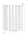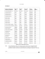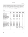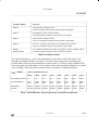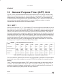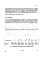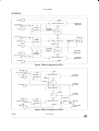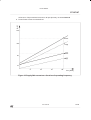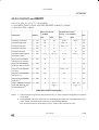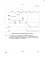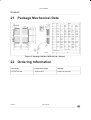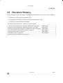
1
ST10F167 16-bit MCU with 128KByte FLASH memory ■ Fast and fl exible bus ● Programmable external bus characteristics for different address ranges ● 8-Bit or 16-Bit external data bus. ● Multiplexed or de-multiplexed external address/data buses ● Five programmable chip-select signals. ● Hold and hold-acknowledge bus arbitration support ■ Fail-safe protection ● Programmable watchdog timer ■ On-chip CAN 2.0B Interface ■ On-chip bootstrap loader ■ Interrupt ● 8-channel PEC for single cycle, interrupt driven data transfer ● 16-priority-level interrupt system with 56 sources, sample-rate down to 50ns ■ Timers ● Two multi-functional general-purpose timer units with 5 timers ● Two 16-bit capture/compare units 42-1701-03 Wdog P.6 P.7 P.3 CAPCOM2 SSC BRG P.5 PWM ASC usart GPT2/GPT1 BRG P.2 Interrupt Controller CAPCOM1 OSC. XRAM 10-Bit ADC ● 2K bytes on-chip internal RAM ● 2K bytes on-chip Extension RAM ● 128K bytes on-chip FLASH memory ● FLASH with 4 independently erasable banks Internal RAM PEC EBC ■ Memory organization CPU-Core CAN ● 16-bit CPU with 4 stage pipeline ● 100ns instruction cycle time at 20MHz CPU clock ● 500ns multiplication (16*16 bit) ● 1µs division (32/16 bit) ● Enhanced boolean bit manipulation facilities ● Additional instructions to support HLL and operating systems ● Single-cycle context switching support P.4 P.1 P.0 ■ High Performance CPU 128Kbyte FLASH DATA SHEET P.8 ■ A/D converter ● 16-channel 10-bit 9.7µs conversion time. ■ Clock Generation ● On-chip PLL. ● Direct clock input ■ Up to 111 General Purpose I/O Lines ■ Programmable threshold (hysteresis) ■ Idle and power down modes ● Idle current <70mA ● Power down supply current <100µA. ■ 4-Channel PWM Unit ■ Serial channels ● Synchronous/asynch serial channel. ● High speed synchronous channel ■ Electrical characteristics ● Power - 5 volt +/- 10% ■ Development support ● C-Compilers, Macro-Assembler Packages, Emulators, Evaluation Boards, HLL-Debuggers, Simulators, Logic Analyzer Disassemblers, Programming Boards ■ Package option ● 144-Pin PQFP Package 10 September 98 DATA SHEET ST10F167 Table of Contents 1 Introduction - - - - - - - - - - - - - - - - - - - - - - - - - - 4 2 Pin Data - - - - - - - - - - - - - - - - - - - - - - - - - - - - 5 3 Functional Description - - - - - - - - - - - - - - - - - - - 12 4 Memory Organization - - - - - - - - - - - - - - - - - - - - 13 5 5.1 5.2 Flash Memory - - - - - - - - - - - - - - - - - - - - - - - - 14 Flash programming and erasing - - - - - - - - - - - - - - - 15 Flash Control Register (FCR) - - - - - - - - - - - - - - - - - 15 5.2.1 Flash memory security - - - - - - - - - - - - - - - - - - - - - - - - 18 6 External Bus Controller - - - - - - - - - - - - - - - - - - - 20 7 Central Processing Unit (CPU) - - - - - - - - - - - - - - - 21 8 Interrupt System - - - - - - - - - - - - - - - - - - - - - - 22 9 Capture/compare (CAPCOM) Units - - - - - - - - - - - - - 26 10 10.1 10.2 General Purpose Timer (GPT) Unit - - - - - - - - - - - - - 28 GPT1 - - - - - - - - - - - - - - - - - - - - - - - - - - - - 28 GPT2 - - - - - - - - - - - - - - - - - - - - - - - - - - - - 29 11 PWM Module - - - - - - - - - - - - - - - - - - - - - - - - 31 12 Parallel Ports - - - - - - - - - - - - - - - - - - - - - - - - 32 13 A/D Converter - - - - - - - - - - - - - - - - - - - - - - - - 33 14 14.1 14.2 Serial Channels - - - - - - - - - - - - - - - - - - - - - - - 34 ASCO - - - - - - - - - - - - - - - - - - - - - - - - - - - - 34 High speed synchronous serial channel (SSC) - - - - - - - - 35 2/78 42-1701-03 DATA SHEET ST10F167 15 Can Module - - - - - - - - - - - - - - - - - - - - - - - - - 36 16 Watchdog Timer 17 Instruction Set 18 Bootstrap Loader - - - - - - - - - - - - - - - - - - - - - - 40 19 Special Function Registers - - - - - - - - - - - - - - - - - 40 20 Electrical Characteristics - - - - - - - - - - - - - - - - - - 48 20.1 20.2 20.3 20.4 20.5 Absolute maximum ratings - Parameter interpretation - - DC Characteristics - - - - - A/D Converter Characteristics AC Characteristics - - - - - - 20.5.1 20.5.2 20.5.3 20.5.4 20.5.5 20.5.6 20.5.7 20.5.8 20.5.9 20.5.10 Test waveforms - - - - Definition of internal timing Direct Drive - - - - - - Phase locked loop - - - External clock drive XTAL1 Memory cycle variables - Multiplexed Bus - - - - Demultiplexed Bus - - - CLKOUT and READY - External Bus Arbitration - - 21 Package Mechanical Data - - - - - - - - - - - - - - - - - - 76 22 Ordering Information - - - - - - - - - - - - - - - - - - - - 76 23 Revision History - - - - - - - - - - - - - - - - - - - - - - 37 - - - - - - - - - - - - - - - - - - - - - - - 38 - - - - - - - - - - - - - - - - - - - - - - - - - - - - - - - - - - 48 48 49 52 54 - 54 54 55 56 57 58 58 65 71 73 - - - - - - - - - - - - - - - - - - - - - - 77 42-1701-03 3/78 DATA SHEET ST10F167 1 Introduction The ST10F167 is a new derivative of the ST Microelectronics 16-bit single-chip CMOS microcontrollers. It combines high CPU performance with high peripheral functionality and enhanced I/O capabilities. It also provides on-chip high-speed RAM and clock generation via PLL. VDD VSS XTAL1 Port 0 16-bit XTAL2 RSTIN RSTOUT Port 1 16-bit VAREF Port 2 16-bit VAGND ST10F167 NMI EA Port 3 15-bit Port 4 8-bit READY Port 6 8-bit ALE RD Port 7 8-bit WR/WRL Port 5 16-bit Port 8 8-bit Figure 1 Logic symbol 4/78 42-1701-03 P6.0/CS0 P6.1/CS1 P6.2/CS2 P6.3/CS3 P6.4/CS4 P6.5/HOLD P6.6/HLDA P6.7/BREQ P8.0/CC16IO P8.1/CC17IO P8.2/CC18IO P8.3/CC19IO P8.4/CC20IO P8.5/CC21IO P8.6/CC22IO P8.7/CC23IO VDD VSS P7.0/POUT0 P7.1/POUT1 P7.2/POUT2 P7.3/POUT3 P7.4/CC28I0 P7.5/CC29I0 P7.6/CC30I0 P7.7/CC31I0 P5.0/AN0 P5.1/AN1 P5.2/AN2 P5.3/AN3 P5.4/AN4 P5.5/AN5 P5.6/AN6 P5.7/AN7 P5.8/AN8 P5.9/AN9 37 38 39 40 41 42 43 44 45 46 47 48 49 50 51 52 53 54 55 56 57 58 59 60 61 62 63 64 65 66 67 68 69 70 71 72 1 2 3 4 5 6 7 8 9 10 11 12 13 14 15 16 17 18 19 20 21 22 23 24 25 26 27 28 29 30 31 32 33 34 35 36 144 143 142 141 140 139 138 137 136 135 134 133 132 131 130 129 128 127 126 125 124 123 122 121 120 119 118 117 116 115 114 113 112 111 110 109 VDD VSS NMI RSTOUT RSTIN VSS XTAL1 XTAL2 VDD P1H.7/A15/CC27IO P1H.6/A14/CC26IO P1H.5/A13/CC25IO P1H.4/A12/CC24IO P1H.3/A11 P1H.2/A10 P1H.1/A9 P1H.0/A8 VSS VDD P1L.7/A7 P1L.6/A6 P1L.5/A5 P1L.4/A4 P1L.3/A3 P1L.2/A2 P1L.1/A1 P1L.0/A0 POH.7/AD15 POH.6/AD14 POH.5/AD13 POH.4/AD12 POH.3/AD11 POH.2/AD10 POH.1/AD9 VSS VDD 2 VAREF VAGND P5.10/AN10/T6EUD P5.11/AN11/T5EUD P5.12/AN12/T6IN P5.13/AN13/T5IN P5.14/AN14/T4EUD P5.15/AN15/T2EUD VSS VDD P2.0/CC0IO P2.1/CC1IO P2.2/CC2IO P2.3/CC3IO P2.4/CC4IO P2.5/CC5IO P2.6/CC6IO P2.7/CC7IO VSS VDD P2.8/CC8IO/EX0IN P2.9/CC9IO/EX1IN P2.10/CC10IOEX2IN P2.11/CC11IOEX3IN P2.12/CC12IO/EX4IN P2.13/CC13IO/EX5IN P2.14/CC14IO/EX6IN P2.15/CC15IO/EX7IN/T7IN P3.0/T0IN P3.1/T6OUT P3.2/CAPIN P3.3/T3OUT P3.4/T3EUD P3.5/T4IN VSS VDD DATA SHEET ST10F167 Pin Data ST10F167 42-1701-03 108 107 106 105 104 103 102 101 100 99 98 97 96 95 94 93 92 91 90 89 88 87 86 85 84 83 82 81 80 79 78 77 76 75 74 73 POH.0/AD8 POL.7/AD7 POL.6/AD6 POL.5/AD5 POL.4/AD4 POL.3/AD3 POL.2AD2 POL.1/AD1 POL.0/AD0 EA ALE READY WR/WRL RD VSS VDD P4.7/A23 P4.6/A22/CAN_TXD P4.5/A21/CAN_RXD P4.4/A20 P4.3/A19 P4.2/A18 P4.1/A17 P4.0/A16 VPP VSS VDD P3.15/CLKOUT P3.13/SCLK P3.12/BHE/WRH P3.11/RXD0 P3.10/TXD0 P3.9/MTSR P3.8/MRST P3.7/T2IN P3.6/T3IN Figure 2 Pin out 5/78 DATA SHEET ST10F167 Symbol P6.0 – P6.7 P8.0 – P8.7 P7.0 – P7.7 Pin Input(I)/ Output(O) 1-8 I/O 1 ... 5 6 7 8 O ... O I O O 9 - 16 I/O 9 ... 16 I/O ... I/O 19 - 26 I/O 19 ... 22 23 ... 26 O ... O I/O ... I/O Function Port 6 is an 8-bit bidirectional I/O port. It is bit-wise programmable for input or output via direction bits. For a pin configured as input, the output driver is put into high-impedance state. Port 6 outputs can be configured as push/pull or open drain drivers. The following Port 6 pins also serve for alternate functions: P6.0 CS0 Chip Select 0 Output ... ... ... P6.4 CS4 Chip Select 4 Output P6.5 HOLD External Master Hold Request Input P6.6 HLDA Hold Acknowledge Output P6.7 BREQ Bus Request Output Port 8 is an 8-bit bidirectional I/O port. It is bit-wise programmable for input or output via direction bits. For a pin configured as input, the output driver is put into high-impedance state. Port 8 outputs can be configured as push/pull or open drain drivers. The input threshold of Port 8 is selectable (TTL or special). The following Port 8 pins also serve for alternate functions: P8.0 CC16IO CAPCOM2: CC16 Cap.-In/Comp.Out ... ... ... P8.7 CC23IO CAPCOM2: CC23 Cap.-In/Comp.Out Port 7 is an 8-bit bidirectional I/O port. It is bit-wise programmable for input or output via direction bits. For a pin configured as input, the output driver is put into high-impedance state. Port 7 outputs can be configured as push/pull or open drain drivers. The input threshold of Port 7 is selectable (TTL or special). The following Port 7 pins also serve for alternate functions: P7.0 POUT0 PWM Channel 0 Output ... ... ... P7.3 POUT3 PWM Channel 3 Output P7.4 CC28IO CAPCOM2: CC28 Cap.-In/Comp.Out ... ... ... P7.7 CC31IO CAPCOM2: CC31 Cap.-In/Comp.Out Table 1 Pin description 6/78 42-1701-03 DATA SHEET ST10F167 Input(I)/ Output(O) Symbol Pin P5.0P5.15 27 – 36 39 – 44 I I 39 40 41 42 43 44 I I I I I I 47 – 54 57 - 64 I/O 47 ... 54 57 I/O ... I/O I/O I ... I/O I I P2.0P2.15 ... 64 Function Port 5 is a 16-bit input-only port with Schmitt-Trigger characteristics. The pins of Port 5 also serve as the (up to 16) analog input channels for the A/D converter, where P5.x equals ANx (Analog input channel x), or they serve as timer inputs: P5.10 T6EUD GPT2 Timer T6 Ext.Up/Down Ctrl.Input P5.11 T5EUD GPT2 Timer T5 Ext.Up/Down Ctrl.Input P5.12 T6IN GPT2 Timer T6 Count Input P5.13 T5IN GPT2 Timer T5 Count Input P5.14 T4EUD GPT1 Timer T4 Ext.Up/Down Ctrl.Input P5.15 T2EUD GPT1 Timer T2 Ext.Up/Down Ctrl.Input Port 2 is a 16-bit bidirectional I/O port. It is bit-wise programmable for input or output via direction bits. For a pin configured as input, the output driver is put into high-impedance state. Port 2 outputs can be configured as push/pull or open drain drivers. The input threshold of Port 2 is selectable (TTL or special). The following Port 2 pins also serve for alternate functions: P2.0 CC0IO CAPCOM: CC0 Cap.-In/Comp.Out ... ... ... P2.7 CC7IO CAPCOM: CC7 Cap.-In/Comp.Out P2.8 CC8IO CAPCOM: CC8 Cap.-In/Comp.Out, EX0IN Fast External Interrupt 0 Input ... ... ... P2.15 CC15IO CAPCOM: CC15 Cap.-In/Comp.Out, EX7IN Fast External Interrupt 7 Input T7IN CAPCOM2 Timer T7 Count Input Table 1 Pin description 42-1701-03 7/78 DATA SHEET ST10F167 Input(I)/ Output(O) Symbol Pin P3.0P3.13, P3.15 65 – 70, 73 – 80, 81 I/O I/O I/O 65 66 67 68 69 70 I O I O I I 73 74 I I 75 76 77 78 79 80 81 I/O I/O O I/O O O I/O O 85 - 92 I/O 85 90 O O I O O O P4.0 – P4.7 91 92 Function Port 3 is a 15-bit (P3.14 is missing) bidirectional I/O port. It is bit-wise programmable for input or output via direction bits. For a pin configured as input, the output driver is put into high-impedance state. Port 3 outputs can be configured as push/pull or open drain drivers. The input threshold of Port 3 is selectable (TTL or special). The following Port 3 pins also serve for alternate functions: P3.0 T0IN CAPCOM Timer T0 Count Input P3.1 T6OUT GPT2 Timer T6 Toggle Latch Output P3.2 CAPIN GPT2 Register CAPREL Capture Input P3.3 T3OUT GPT1 Timer T3 Toggle Latch Output P3.4 T3EUD GPT1 Timer T3 Ext.Up/Down Ctrl.Input P3.5 T4IN GPT1 Timer T4 Input for Count/Gate/Reload/Capture P3.6 T3IN GPT1 Timer T3 Count/Gate Input P3.7 T2IN GPT1 Timer T2 Input for Count/Gate/Reload/Capture P3.8 MRST SSC Master-Rec./Slave-Transmit I/O P3.9 MTSR SSC Master-Transmit/Slave-Rec. O/I P3.10 TxD0 ASC0 Clock/Data Output (Asyn./Syn.) P3.11 RxD0 ASC0 Data Input (Asyn.) or I/O (Syn.) P3.12 BHE Ext. Memory High Byte Enable Signal, WRH Ext. Memory High Byte Write Strobe P3.13 SCLK SSC Master Clock Outp./Slave Cl. Inp. P3.15 CLKOUT System Clock Output (=CPU Clock) Port 4 is an 8-bit bidirectional I/O port. It is bit-wise programmable for input or output via direction bits. For a pin configured as input, the output driver is put into high-impedance state. In case of an external bus configuration, Port 4 can be used to output the segment address lines: P4.0 A16 Least Significant Segment Addr. Line P4.5 A21 Segment Address Line, CAN_RxD CAN Receive Data Input P4.6 A22 Segment Address Line, CAN_TxD CAN Transmit Data Output P4.7 A23 Most Significant Segment Addr. Line Table 1 Pin description 8/78 42-1701-03 DATA SHEET ST10F167 Symbol Pin Input(I)/ Output(O) Function RD 95 O External Memory Read Strobe. RD is activated for every external instruction or data read access. WR/ WRL 96 O External Memory Write Strobe. In WR-mode this pin is activated for every external data write access. In WRL-mode this pin is activated for low byte data write accesses on a 16-bit bus, and for every data write access on an 8-bit bus. See WRCFG in register SYSCON for mode selection. READY 97 I Ready Input. When the Ready function is enabled, a high level at this pin during an external memory access will force the insertion of memory cycle time waitstates until the pin returns to a low level. ALE 98 O Address Latch Enable Output. Can be used for latching the address into external memory or an address latch in the multiplexed bus modes. EA 99 I External Access Enable pin. A low level at this pin during and after Reset forces the ST10F167 to begin instruction execution out of external memory. A high level forces execution out of the internal Flash Memory. I/O PORT0 consists of the two 8-bit bidirectional I/O ports P0L and P0H. It is bit-wise programmable for input or output via direction bits. For a pin configured as input, the output driver is put into high-impedance state. In case of an external bus configuration, PORT0 serves as the address (A) and address/data (AD) bus in multiplexed bus modes and as the data (D) bus in demultiplexed bus modes. Demultiplexed bus modes: Data Path Width: 8-bit 16-bit P0L.0 – P0L.7: D0 – D7 D0 - D7 P0H.0 – P0H.7: I/O D8 - D15 Multiplexed bus modes: Data Path Width: 8-bit 16-bit P0L.0 – P0L.7: AD0 – AD7 AD0 - AD7 P0H.0 – P0H.7: A8 - A15 AD8 - AD15 PORT0: P0L.0P0L.7 P0H.0P0H.7 100-107 108, 111-117 Table 1 Pin description 42-1701-03 9/78 DATA SHEET ST10F167 Symbol PORT1: P1L.0 – P1L.7, P1H.0 P1H.7 Pin Input(I)/ Output(O) I/O 118 – 125 128 – 135 Function PORT1 consists of the two 8-bit bidirectional I/O ports P1L and P1H. It is bit-wise programmable for input or output via direction bits. For a pin configured as input, the output driver is put into high-impedance state. PORT1 is used as the 16-bit address bus (A) in demultiplexed bus modes and also after switching from a demultiplexed bus mode to a multiplexed bus mode. The following PORT1 pins also serve for alternate functions: P1H.4 CC24IO CAPCOM2: CC24 Capture Input P1H.5 CC25IO CAPCOM2: CC25 Capture Input P1H.6 CC26IO CAPCOM2: CC26 Capture Input P1H.7 CC27IO CAPCOM2: CC27 Capture Input 132 133 134 135 I I I I XTAL1 138 I XTAL2 137 O RSTIN 140 I Reset Input with Schmitt-Trigger characteristics. A low level at this pin for a specified duration while the oscillator is running resets the ST10F167. An internal pullup resistor permits power-on reset using only a capacitor connected to VSS. RSTOUT 141 O Internal Reset Indication Output. This pin is set to a low level when the part is executing, either a hardware, a software or a watchdog timer reset. RSTOUT remains low until the EINIT (end of initialization) instruction is executed. NMI 142 I Non-Maskable Interrupt Input. A high to low transition at this pin causes the CPU to vector to the NMI trap routine. When the PWRDN (power down) instruction is executed, the NMI pin must be low in order to force the ST10F167 to go into power down mode. If NMI is high, when PWRDN is executed, the part will continue to run in normal mode. If not used, pin NMI should be pulled high externally. VAREF 37 - Reference voltage for the A/D converter. VAGND 38 - Reference ground for the A/D converter. XTAL1: Input to the oscillator amplifier and input to the internal clock generator XTAL2: Output of the oscillator amplifier circuit. To clock the device from an external source, drive XTAL1, while leaving XTAL2 unconnected. Minimum and maximum high/low and rise/fall times specified in the AC Characteristics must be observed. Table 1 Pin description 10/78 42-1701-03 DATA SHEET ST10F167 Symbol Pin Input(I)/ Output(O) Function VPP 84 - Flash programming voltage. This pin accepts the programming voltage for the on-chip flash EPROM of the ST10F167. VDD 46, 82, 136 - Digital Supply Voltage for internal circuitry: + 5 V during normal operation and idle mode. 2.5 V during power down mode 17, 56, 72, 93, 109,126 ,144 - Digital Supply Voltage for port drivers: + 5 V during normal operation and idle mode 45, 83, 139 - Digital Ground for internal circuitry. 18, 55, 71, 94, 110,127 ,143 - Digital Ground for port drivers. VSS Table 1 Pin description 42-1701-03 11/78 DATA SHEET ST10F167 3 Functional Description The architecture of the ST10F167 combines advantagesof both RISC and CISC processors and an advanced peripheral subsystem. The following block diagram gives an overview of the different on-chip components and the high bandwidth internal bus structure of the ST10F167. 16 Internal FLASH Memory 32 Internal RAM 16 CPU-Core Watchdog 16 PEC OSC. 16 XRAM Interrupt Controller 16 8 Port 6 8 Port 5 16 BRG Port 2 CAPCOM1 CAPCOM2 BRG Port 3 15 Figure 3 Block diagram 12/78 PWM SSC ASC usart GPT1 GPT2 10-Bit ADC 16 External Bus Controller 16 Port 4 Port 1 Port 0 CAN 42-1701-03 Port 7 8 Port 8 8 16 DATA SHEET ST10F167 4 Memory Organization The memory space of the ST10F167 is configured in a Von-Neumann architecture. Code memory, data memory, registers and I/O ports are organized within the same linear address space of 16 MBytes. The entire memory space can be accessed bytewise or wordwise. Particular portions of the on-chip memory have additionally been made directly bit addressable. The ST10F167 provides 128KBytes of on-chip flash memory. 2 KBytes of on-chip Internal RAM stores user defi ned variables for the system stack, general purpose register banks and even for code. A register bank can consist of up to 16 wordwide (R0 to R15) and/or bytewide (RL0, RH0, …, RL7, RH7) so-called General Purpose Registers (GPRs). 1024 bytes (2 * 512 bytes) of the address space are reserved for the Special Function Register areas (SFR space and ESFR space). SFRs are wordwide registers which are used for controlling and monitoring functions of the different on-chip units. Unused SFR addresses are reserved for other/future members of the ST10 family. 2 KBytes of on-chip Extension RAM (XRAM) are provided to store user data, user stacks or code. The XRAM is accessed like external memory and cannot be used for the system stack or register banks, and is not bit-addressable. The XRAM allows 16-bit accesses with maximum speed. In order to meet the needs of designs where more memory is required than is provided on chip, up to 16 MBytes of external RAM and/or ROM can be connected to the microcontroller. 42-1701-03 13/78 DATA SHEET ST10F167 5 Flash Memory The ST10F167 provides 128KBytes of on-chip, electrically erasable and re-programmable Flash EPROM. The fl ash memory is organized in 32 bit wide blocks. Double word instructions can be fetched in one machine cycle. The fl ash memory can be used for both code and data storage. It is into four banks of sizes 8K, 24K, 48K and 48Kbytes. Each of these banks can be erased independently. This prevents unnecessary re-programming of the whole fl ash memory when only a partial re-programming is required. The fi rst 32K bytes of the FLASH memory are located in segment 0 (0h to 007FFFh) during reset, and include the reset and interrupt vectors. The rest of the FLASH memory is mapped in segments 1 and 2 (018000h to 02FFFFh). For fl exibility, the fi rst 32K bytes of the FLASH memory may be remapped to segment 1 (010000h to 017FFFh) during initialization. This allows the interrupt vectors to be programmed from the external memory, while retaining the common routines and constants that are programmed into the FLASH memory. Bank Addresses (Segment 0) Size (bytes) 0 000000h to 07FFFh and 018000h to 01BFFFh 48K 1 01C000h to 027FFFh 48K 2 028000h to 02DFFFh 24K 3 02E000h to 02FFFFh 8K Table 2 Flash memory bank addresses 14/78 42-1701-03 DATA SHEET ST10F167 5.1 Flash programming and erasing The FLASH memory is programmedusing the PRESTO F ProgramWrite algorithm. Erasure of the FLASH memory is performed in the program mode using the PRESTO F Erase algorithm. Timing of the Write/Erase cycles is automatically generated by a programmable timer and completion is indicated by a fl ag. A second flag indicates that the VPP voltage was correct for the whole programming cycle. This guarantees that a good write/erase operation has been carried out. Parameter Units Min Typical Max Word Programming Time µsec 12.8 12.8 1250 Bank Erasing Time sec 0.5 30 Endurance cycles 1000 Flash Vpp volts 11.4 12.6 Table 3 Flash Parameters 5.2 Flash Control Register (FCR) In the standard operation mode, the FLASH memory can be accessed in the same way as the normal mask-programmable on-chip ROM. All, appropriate, direct and indirect addressing modes can be used for reading the FLASH memory. All programming or erase operations are controlled via a 16-bit register, the FCR. The FCR is not an SFR or GPR. To prevent inadvertent writing to the FLASH memory, the FCR is locked and inactive during the standard operation mode. The FLASH memory writing mode must be entered, before a valid access to the FCR is provided. This is done via a special key code instruction sequence. The FCR is virtually mapped into the active address space of the Flash memory. It can only be accessed with direct 16-bit (mem) addressing modes. Since the FCR is neither byte, nor bit-addressable, only word operand instructions can be used for FCR accesses. By default, the FCR can be accessed with any even address from 000000h to 07FFFEh and 018000h to 02FFFEh. If the first 32K byte Block of the FLASH memory is mapped to segment 1, the corresponding even FCR addresses are 010000h to 017FFEh. Note that DPP referencing and DPP contents must be considered for FCR accesses. If an FCR access is attempted via an odd address, an illegal operand access hardware trap will occur. FCR Flash Control Register: Reset Condition: 0000h (Read) 42-1701-03 15/78 DATA SHEET ST10F167 Bit number & name Description b15 = FWMSET This bit is set to ”1” automatically once the Flash writing mode is entered. To exit from the Flash writing mode, FWMSET must be set to ”0”. Since only word values can be written to FCR, care must be taken that FWMSET is not cleared inadvertently. Therefore, for any command written to FCR (except for the return to the Flash standard mode), FWMSET must be set to ”1”. Reset condition of FWMSET is ”0”. Flash Writing Mode Set. b14-b10 These bits are reserved for future development, they must be written to ”0”. b9-b8 = BE0,1 Select the Flash memory bank to be erased. The physical addresses of bank 0 depends on the which Flash memory map has been chosen. In Flash operating modes, other than the erasing mode, these bits are not signifi cant. At reset BE1,0 are set to ”00”. Bank erase select. b7 = WDWW Word/double word write. b6-b5 = CKCTL0,1 Flash Timer Clock Control. Determines the word width used for programming operations: 16-bit (WDWW = 0) or 32-bit (WDWW = ”1”). In Flash operation modes, other than the programming mode, this bit is not signifi cant. At reset, WDWW is set to “0”. Control the width (TPRG) of the programming or erase pulses applied to the Flash memory cells during the operation. TPRG varies in an inverse ratio to the clock frequency. To avoid putting the Flash memory under critical stress conditions, the width of one single programming or erase pulse and the programming or erase time, must not exceed defi ned values. Thus the maximum number of programming or erase attempts, depends on the system clock frequency. RESET state: 00. b4 = VPPRIV VPP Revelation bit. Read-only bit refl ects the state of the VPP voltage in the Flash writing mode. If VPPRIV is set to ”0”, this indicates that V PP is below the threshold necessary for reliable programming. The normal reaction to this indication is to check the VPP power supply and to then repeat the intended operation. If the VPP voltage is above a suffi cient margin, VPPRIV will be set to ”1”. The reset state of the VPPRIV bit depends on the state of the external VPP voltage at the VPP pin. Table 4 Flash control register bit definition 16/78 42-1701-03 DATA SHEET ST10F167 Bit number & name Description b3 = FCVPP Read-only bit indicates that the VPP voltage fell below the valid threshold value during a Flash programming or erase operation. If FCVPP is set to ”1” after such an operation has fi nished, it can mean that the operation was not successful. The VPP power supply should be checked and the operation repeated. If FCVPP is set to ”0”, no critical discontinuity in VPP occurred. At reset FCVPP is set to ”0”. Flash VPP control bit. b2 = FBUSY Flash busy bit. b2 = RPROT Protection enable bit. b1 = FEE Flash erase/program selection. b0 = FWE Flash write/read enable. Read-only bit indicates that a Flash programming or erase operation is in progress. FBUSY is set to ”1” by hardware, as soon as the programming or erase command is given. At reset FBUSY is set to ”0”. Note that this bit position is also occupied by the write-only bit RPROT. This bit set at 1, anded with the OTP protection bit, disables any access to the Flash, by instructions fetched from the external memory space, or from the internal RAM. This write-only bit, is only signifi cant if the general Flash memory protection is enabled. If the protection is enabled, the setting of RPROT determines whether the Flash protection is active (RPROT=”1”) or inactive (RPROT=”0”). RPROT is the only FCR bit which can be modifi ed even in the Flash standard operation mode, but only by an instruction executed from the Flash memory itself. At reset, RPROT is set to ”1”. Note that this bit position is also occupied by the read-only bit FBUSY. Selects the Flash write operation to be performed: erase (FEE=”1”) or programming (FEE=”0”). Together with bits FWE and FWMSET, bit FEE determined the operation mode of the Flash memory. Note that setting bits FWE and FEE causes the corresponding Flash operation mode to be selected but does not launch the execution of the selected operation. If bit FWE was set to ”0”, the setting of FEE is insignifi cant. At reset, FEE is set to ”0”. This bit determines whether FLASH write operations are enabled (FWE=1) or disabled (FWE=0). By defi nition, a FLASH write operation can be either programming or erasure. Together with bits FEE and FWMSET, bit FWE determines the operation mode of the Flash memory. Note that setting bits FWE and FEE causes the corresponding Flash operation mode to be selected but does not launch the execution of the selected operation. If bit FWE was set to ”1”, any read access on a Flash memory location means a particular program-verify or erase-verify read operation. Flash write operations are disabled at reset. Table 4 Flash control register bit definition 42-1701-03 17/78 DATA SHEET ST10F167 5.2.1 Flash memory security Security and reliability have been enhanced by built-in features: a key code sequence is used to enter the Write/Erase mode preventing false write cycles, a programmable option (set by the programming board) prevents access to the FLASH memory from the internal RAM or from External Memory. If the security option is set, the FLASH memory can only be accessed from a program within the FLASH memory area. This protection can only be disabled by instructions executed from the FLASH memory. =0 PCOUNT=PNmax? PCOUNT=PCOUNT+1 VR02057A Figure 4 PRESTO F write algorithm 18/78 42-1701-03 DATA SHEET ST10F167 =0 PCOUNT=ENmax? PCOUNT=PCOUNT+1 VR02057B Figure 5 PRESTO F erase algorithm 42-1701-03 19/78 DATA SHEET ST10F167 6 External Bus Controller All of the external memory accesses are performed by the on-chip External Bus Controller (EBC). It can be programmed either to single chip mode when no external memory is required, or to one of four different external memory access modes: • 16-/18-/20-/24-bit Addresses, 16-bit Data, Demultiplexed • 16-/18-/20-/24-bit Addresses, 16-bit Data, Multiplexed • 16-/18-/20-/24-bit Addresses, 8-bit Data, Multiplexed • 16-/18-/20-/24-bit Addresses, 8-bit Data, Demultiplexed In the demultiplexed bus modes, addresses are output on PORT1 and data is input/output on PORT0. In the multiplexed bus modes both addresses and data use PORT0 for input/ output. Important timing characteristics of the external bus interface (Memory Cycle Time, Memory Tri-State Time, Length of ALE and Read Write Delay) have been made programmable. This gives the choice of a wide range of different types of memories and external peripherals. In addition, different address ranges may be accessed with different bus characteristics. Up to 5 external CS signals (4 windows plus default) can be generated in order to save external glue logic. Access to very slow memories is supported via a particular ‘Ready’ function. A HOLD/HLDA protocol is available for bus arbitration. For applications which require less than 16 MBytes of external memory space, this address space can be restricted to 1 MByte, 256 KByte or to 64 KByte. In this case Port 4 outputs four, two or no address lines. If an address space of 16 MBytes is used, it outputs all 8 address lines. 20/78 42-1701-03 DATA SHEET ST10F167 7 Central Processing Unit (CPU) CPU FLASH ROM 32 SP STKOV STKUN Exec. Unit Instr. Ptr Instr. Reg 4-Stage Pipeline PSW SYSCON BUSCON 0 BUSCON 1 BUSCON 2 BUSCON 3 BUSCON 4 Data Pg. Ptrs 16 MDH MLD Mul./Div.-HW Bit-Mask Gen. R15 Internal RAM 2KByte General ALU 16-Bit Purpose R15 Registers Barrel-Shift Context Ptr ADDRSEL 1 ADDRSEL 2 ADDRSEL 3 ADDRSEL 4 Code Seg. Ptr. R0 16 R0 Figure 6 CPU block diagram The CPU includes a 4-stage instruction pipeline, a 16-bit arithmetic and logic unit (ALU). Dedicated SFRs have been added for a separate multiply and divide unit, a bit-mask generator and a barrel shifter. Most of the ST10F167’s instructions can be executed in one instruction cycle which requires 100ns at 20MHz CPU clock. For example, shift and rotate instructions are always processed in one machine cycle independent of the number of bits to be shifted. All multiple-cycle instructions have been optimized for speed: branches in 2 cycles, a 16 X 16 bit multiplication in 5 cycles and a 32-/16 bit division in 10 cycles. The ‘Jump Cache’ pipeline optimization, reduces the execution time of repeatedly performed jumps in a loop, from 2 cycles to 1 cycle. The CPU includes an actual register context. This consists of up to 16 wordwide GPRs which are physically allocated within the on-chip RAM area. A Context Pointer (CP) register determines the base address of the active register bank to be accessed by the CPU at a time. The number of register banks is only restricted by the available internal RAM space. For easy parameter passing, a register bank may overlap others. A system stack of up to 2048 bytes is provided as a storage for temporary data. The system stack is allocated in the on-chip RAM area, and it is accessed by the CPU via the stack pointer (SP) register. Two separate SFRs, STKOV and STKUN, are implicitly compared against the stack pointer value upon each stack access for the detection of a stack overflow or underflow. 42-1701-03 21/78 DATA SHEET ST10F167 8 Interrupt System With an interrupt response time from 250ns to 600ns (in the case of internal program execution), the ST10F167 reacts quickly to the occurrence of non-deterministic events The architecture of the ST10F167 supports several mechanisms for fast and flexible response to service requests that can be generated from various sources internal or external to the microcontroller. Any of these interrupt requests can be programmed to being serviced by the Interrupt Controller or by the Peripheral Event Controller (PEC). In a standard interrupt service, program execution is suspended and a branch to the interrupt vector table is performed. For a PEC service, just one cycle is ‘stolen’ from the current CPU activity. A PEC service is a single byte or word data transfer between any two memory locations with an additional increment of either the PEC source or the destination pointer. An individual PEC transfer counter is decremented for each PEC service, except for the continuous transfer mode. When this counter reaches zero, a standard interrupt is performed to the corresponding source related vector location. PEC services are suited to, for example, the transmission or reception of blocks of data. The ST10F167 has 8 PEC channels, each of which offers fast interrupt-driven data transfer capabilities. A separate control register which contains an interrupt request fl ag, an interrupt enable fl ag and an interrupt priority bitfield, exists for each of the possible interrupt sources. Via its related register, each source can be programmed to one of sixteen interrupt priority levels. Once having been accepted by the CPU, an interrupt service can only be interrupted by a higher prioritized service request. For the standard interrupt processing, each of the possible interrupt sources has a dedicated vector location. Fast external interrupt inputs are provided to service external interrupts with high precision requirements. These fast interrupt inputs, feature programmable edge detection (rising edge, falling edge or both edges). Software interrupts are supported by means of the ‘TRAP’ instruction in combination with an individual trap (interrupt) number. The table below shows all of the possible ST10F167 interrupt sources and the corresponding hardware-related interrupt flags, vectors, vector locations and trap (interrupt) numbers. Source of Interrupt or PEC Service Request Request Flag Enable Flag Interrupt Vector Vector Location Trap Number CAPCOM Register 0 CC0IR CC0IE CC0INT 00’0040h 10h CAPCOM Register 1 CC1IR CC1IE CC1INT 00’0044h 11h Table 5 List of interrupt sources 22/78 42-1701-03 DATA SHEET ST10F167 Source of Interrupt or PEC Service Request Request Flag Enable Flag Interrupt Vector Vector Location Trap Number CAPCOM Register 2 CC2IR CC2IE CC2INT 00’0048h 12h CAPCOM Register 3 CC3IR CC3IE CC3INT 00’004Ch 13h CAPCOM Register 4 CC4IR CC4IE CC4INT 00’0050h 14h CAPCOM Register 5 CC5IR CC5IE CC5INT 00’0054h 15h CAPCOM Register 6 CC6IR CC6IE CC6INT 00’0058h 16h CAPCOM Register 7 CC7IR CC7IE CC7INT 00’005Ch 17h CAPCOM Register 8 CC8IR CC8IE CC8INT 00’0060h 18h CAPCOM Register 9 CC9IR CC9IE CC9INT 00’0064h 19h CAPCOM Register 10 CC10IR CC10IE CC10INT 00’0068h 1Ah CAPCOM Register 11 CC11IR CC11IE CC11INT 00’006Ch 1Bh CAPCOM Register 12 CC12IR CC12IE CC12INT 00’0070h 1Ch CAPCOM Register 13 CC13IR CC13IE CC13INT 00’0074h 1Dh CAPCOM Register 14 CC14IR CC14IE CC14INT 00’0078h 1Eh CAPCOM Register 15 CC15IR CC15IE CC15INT 00’007Ch 1Fh CAPCOM Register 16 CC16IR CC16IE CC16INT 00’00C0h 30h CAPCOM Register 17 CC17IR CC17IE CC17INT 00’00C4h 31h CAPCOM Register 18 CC18IR CC18IE CC18INT 00’00C8h 32h CAPCOM Register 19 CC19IR CC19IE CC19INT 00’00CCh 33h CAPCOM Register 20 CC20IR CC20IE CC20INT 00’00D0h 34h CAPCOM Register 21 CC21IR CC21IE CC21INT 00’00D4h 35h CAPCOM Register 22 CC22IR CC22IE CC22INT 00’00D8h 36h CAPCOM Register 23 CC23IR CC23IE CC23INT 00’00DCh 37h CAPCOM Register 24 CC24IR CC24IE CC24INT 00’00E0h 38h CAPCOM Register 25 CC25IR CC25IE CC25INT 00’00E4h 39h CAPCOM Register 26 CC26IR CC26IE CC26INT 00’00E8h 3Ah CAPCOM Register 27 CC27IR CC27IE CC27INT 00’00ECh 3Bh CAPCOM Register 28 CC28IR CC28IE CC28INT 00’00E0h 3Ch CAPCOM Register 29 CC29IR CC29IE CC29INT 00’0110h 44h CAPCOM Register 30 CC30IR CC30IE CC30INT 00’0114h 45h Table 5 List of interrupt sources 42-1701-03 23/78 DATA SHEET ST10F167 Source of Interrupt or PEC Service Request Request Flag Enable Flag Interrupt Vector Vector Location Trap Number CAPCOM Register 31 CC31IR CC31IE CC31INT 00’0118h 46h CAPCOM Timer 0 T0IR T0IE T0INT 00’0080h 20h CAPCOM Timer 1 T1IR T1IE T1INT 00’0084h 21h CAPCOM Timer 7 T7IR T7IE T7INT 00’00F4h 3Dh CAPCOM Timer 8 T8IR T8IE T8INT 00’00F8h 3Eh GPT1 Timer 2 T2IR T2IE T2INT 00’0088h 22h GPT1 Timer 3 T3IR T3IE T3INT 00’008Ch 23h GPT1 Timer 4 T4IR T4IE T4INT 00’0090h 24h GPT2 Timer 5 T5IR T5IE T5INT 00’0094h 25h GPT2 Timer 6 T6IR T6IE T6INT 00’0098h 26h GPT2 CAPREL Register CRIR CRIE CRINT 00’009Ch 27h A/D Conversion Complete ADCIR ADCIE ADCINT 00’00A0h 28h A/D Overrun Error ADEIR ADEIE ADEINT 00’00A4h 29h ASC0 Transmit S0TIR S0TIE S0TINT 00’00A8h 2Ah ASC0 Transmit Buffer S0TBIR S0TBIE S0TBINT 00’011Ch 47h ASC0 Receive S0RIR S0RIE S0RINT 00’00ACh 2Bh ASC0 Error S0EIR S0EIE S0EINT 00’00B0h 2Ch SSC Transmit SCTIR SCTIE SCTINT 00’00B4h 2Dh SSC Receive SCRIR SCRIE SCRINT 00’00B8h 2Eh SSC Error SCEIR SCEIE SCEINT 00’00BCh 2Fh PWM Channel 0...3 PWMIR PWMIE PWMINT 00’00FCh 3Fh CAN Interface XP0IR XP0IE XP0INT 00’0100h 40h X-Peripheral Node XP1IR XP1IE XP1INT 00’0104h 41h X-Peripheral Node XP2IR XP2IE XP2INT 00’0108h 42h PLL Unlock XP3IR XP3IE XP3INT 00’010Ch 43h Table 5 List of interrupt sources Note 24/78 Two X-Peripheral nodes can accept interrupt requests from integrated X-Bus peripherals. Nodes, where no X-Peripherals are connected, may be used to generate software controlled interrupt requests by setting the respective XPnIR bit. 42-1701-03 DATA SHEET ST10F167 The ST10F167 identifies and to processes exceptions or error conditions that arise during run-time, ‘Hardware Traps’. Hardware traps cause an immediate non-maskable system reaction which is similar to a standard interrupt service (branching to a dedicated vector table location). The occurrence of a hardware trap is additionally signified by an individual bit in the trap fl ag register (TFR). Except when another higher prioritized trap service is in progress, a hardware trap will interrupt any actual program execution. In turn, hardware trap services can normally not be interrupted by standard or PEC interrupts The table below shows all of the possible exceptions or error conditions that can arise during run-time. Trap Vector Vector Location Trap Number Trap Priority Hardware Reset RESET 00’0000h 00h III Software Reset RESET 00’0000h 00h III Watchdog Timer Overfl ow RESET 00’0000h 00h III Exception Condition Trap Flag Reset Functions: Class A Hardware Traps: Non-Maskable Interrupt NMI NMITRAP 00’0008h 02h II Stack Overfl ow STKOF STOTRAP 00’0010h 04h II Stack Underfl ow STKUF STUTRAP 00’0018h 06h II Undefi ned Opcode UNDOPC BTRAP 00’0028h 0Ah I Protected Instruction Fault PRTFLT BTRAP 00’0028h 0Ah I Illegal Word Operand Access ILLOPA BTRAP 00’0028h 0Ah I Illegal Instruction Access ILLINA BTRAP 00’0028h 0Ah I Illegal External Bus Access ILLBUS BTRAP 00’0028h 0Ah I Reserved [2Ch –3Ch] [0Bh – 0Fh] Software Traps: Any Any [00’0000h– [00h – 7Fh] 00’01FCh] in steps of 4h Class B Hardware Traps: TRAP Instruction 42-1701-03 Current CPU Priority 25/78 DATA SHEET ST10F167 9 Capture/compare (CAPCOM) Units The CAPCOM units support generation and control of timing sequences on up to 32 channels. It has a maximum resolution of 400 ns at 20MHz CPU clock. The CAPCOM units are typically used to handle high speed I/O tasks such as pulse and waveform generation, pulse width modulation (PMW), Digital to Analog (D/A) conversion, software timing, or time recording relative to external events. Four 16-bit timers (T0/T1, T7/T8) with reload registers, provide two independent time bases for the capture/compare register array. The input clock for the timers is programmable to several pre-scaled values of the internal system clock, or may be derived from an overflow/underflow of timer T6 in module GPT2. This provides a wide range of variation for the timer period and resolution and allows precise adjustments to the application specific requirements. In addition, external count inputs for CAPCOM timers T0 and T7 allow event scheduling for the capture/compare registers relative to external events. Both of the two capture/compare register arrays contain 16 dual purpose capture/compare registers, each of which may be individually allocated to either CAPCOM timer T0 or T1 (T7 or T8, respectively), and programmed for capture or compare function. Each register has one port pin associated with it which serves as an input pin for triggering the capture function, or as an output pin (except for CC24...CC27) to indicate the occurrence of a compare event. When a capture/compare register has been selected for capture mode, the current contents of the allocated timer will be latched (‘captured) into the capture/compare register in response to an external event at the port pin which is associated with this register. In addition, a specifi c interrupt request for this capture/compare register is generated. Either a positive, a negative, or both a positive and a negative external signal transition at the pin can be selected as the triggering event. The contents of all registers which have been selected for one of the five compare modes are continuously compared with the contents of the allocated timers. When a match occurs between the timer value and the value in a capture/ compare register, specific actions will be taken, based on the selected compare mode. 26/78 42-1701-03 DATA SHEET ST10F167 Compare Modes Function Mode 0 Interrupt-only compare mode; several compare interrupts per timer period are possible Mode 1 Pin toggles on each compare match; several compare events per timer period are possible Mode 2 Interrupt-only compare mode; only one compare interrupt per timer period is generated Mode 3 Pin set ‘1’ on match; pin reset ‘0’ on compare time overfl ow; only one compare event per timer period is generated Double Register Mode Two registers operate on one pin; pin toggles on each compare match; several compare events per timer period are possible. Table 6 Compare modes The input frequencies fTx for Tx are determined as a function of the CPU clocks. The formulas are detailed in the user manual. The timer input frequencies, resolution and periods which result from the selected pre-scaler option in TxI when using a 20MHz CPU clock are listed in the table below. The numbers for the timer periods are based on a reload value of 0000H. Note that some numbers may be rounded to 3 significant fi gures. fCPU = 20MHz Timer Input Selection TxI 000B 001B 010B 011B 100B 101B 110B 111B Pre-scaler for fCPU 8 16 32 64 128 256 512 1024 Input Frequency 2.5 MHz 1.25 MHz 625 kHz 313 kHz 156 kHz 78.1 kHz 39.1 kHz 19.5 kHz Resolution 400ns 800ns 1.60µs 3.20µs 6.40µs 12.8µs 25.6µs 51.2µs Period 26.2ms 52.4ms 105ms 210ms 419ms 839ms 1.68s 3.36s Table 7 CAPCOM timer input frequencies, resolution and periods 42-1701-03 27/78 DATA SHEET ST10F167 10 General Purpose Timer (GPT) Unit The GPT unit is a flexible multifunctional timer/counter structure. It may be used for many different time-related tasks such as: event timing and counting, pulse width and duty cycle measurements, pulse generation or pulse multiplication. The GPT unit incorporates five 16-bit timers which are organized in two separate modules, GPT1 and GPT2. Each timer, in each module may operate independently in a number of different modes, or may be concatenated with another timer of the same module. 10.1 GPT1 Each of the three timers T2, T3, T4 of module GPT1 can be configured individually for one of three basic modes of operation: timer, gated timer, and counter mode. In timer mode, the input clock for a timer is derived from the CPU clock, divided by a programmable prescaler. counter mode allows a timer to be clocked in reference to external events. Pulse width or duty cycle measurement is supported in gated timer mode where the operation of a timer is controlled by the ‘gate’ level on an external input pin. Each timer has one associated port pin (TxIN) which serves as gate or clock input. Table 8 GPT1 timer input frequencies, resolution and periods lists the timer input frequencies, resolution and periods for each pre-scaler option at 25 MHz CPU clock. This also applies to the Gated Timer Mode of T3 and to the auxiliary timers T2 and T4 in Timer and Gated Timer Mode. fCPU = 20MHz Timer Input Selection T2I / T3I / T4I 000B 001B 010B 011B 100B 101B 110B 111B Pre scaler 8 16 32 64 128 256 512 1024 Input Frequency 2.5 MHz 1.25 MHz 625 kHz 313 kHz 156 kHz 78.1 kHz 39.1 kHz 19.5 kHz Resolution 400ns 800ns 1.60µs 3.20µs 6.40µs 12.8µs 25.6µs 51.2µs Period 26.2ms 52.4ms 105ms 210ms 419ms 839ms 1.68s 3.36s Table 8 GPT1 timer input frequencies, resolution and periods The count direction (up/down) for each timer is programmable by software or may be altered dynamically by an external signal on a port pin (TxEUD) to facilitate, for example, position tracking. Timer T3 has output toggle latches (TxOTL) which changes state on each timer over-flow/ underfl ow. The state of this latch may be output on port pins (TxOUT) e. g. for time out monitoring of external hardware components, or may be used internally to clock timers T2 and T4 for measuring long time periods with high resolution. 28/78 42-1701-03 DATA SHEET ST10F167 In addition to their basic operating modes, timers T2 and T4 may be confi gured as reload or capture registers for timer T3. When used as capture or reload registers, timers T2 and T4 are stopped. The contents of timer T3 are captured into T2 or T4 in response to a signal at their associated input pins (TxIN). Timer T3 is reloaded with the contents of T2 or T4, triggered, either by an external signal, or by a selectable state transition of its toggle latch T3OTL. When both T2 and T4 are configured to alternately reload T3 on opposite state transitions of T3OTL with the low and high times of a PWM signal, this signal can be constantly generated without software intervention. 10.2 GPT2 The GPT2 module provides precise event control and time measurement. It includes two timers (T5, T6) and a capture/reload register (CAPREL). Both timers can be clocked with an input clock which is derived from the CPU clock via a programmable prescaler or with external signals. The count direction (up/down) for each timer is programmable by software or may additionally be altered dynamically by an external signal on a port pin (TxEUD). Concatenation of the timers is supported by the output toggle latch (T6OTL) of timer T6, which changes its state on each timer overflow/underflow. The state of this latch may be used to clock timer T5, or it may be output on a port pin (T6OUT). The overflows/underflows of timer T6 can additionally be used to clock the CAPCOM timers T0 or T1, and to cause a reload from the CAPREL register. The CAPREL register may capture the contents of timer T5 based on an external signal transition on the corresponding port pin (CAPIN), and timer T5 may optionally be cleared after the capture procedure. This allows absolute time differences to be measured or pulse multiplication to be performed without software overhead. Table 9 GPT2 timer input frequencies, resolution and period lists the timer input frequencies, resolution and periods for each pre-scaler option at 25 MHz CPU clock. This also applies to the Gated Timer Mode of T6 and to the auxiliary timer T5 in Timer and Gated Timer Mode. fCPU = 20MHz Timer Input Selection T5I / T6I 000B 001B 010B 011B 100B 101B 110B 111B Pre-scaler factor 4 8 16 32 64 128 256 512 Input Frequency 5 MHz 2.5 MHz 1.25 MHz 625 kHz 313 kHz 156 kHz 78.1 kHz 39.1 kHz Resolution 200ns 400ns 800ns 1.60µs 3.20µs 6.40µs 12.8µs 25.6µs Period 13.11ms 26.2ms 52.4ms 105ms 210ms 419ms 839ms 1.68s Table 9 GPT2 timer input frequencies, resolution and period 42-1701-03 29/78 DATA SHEET ST10F167 T2EUD U/D Interrupt Request GPT1 Timer T2 CPU Clock 2n n=3...10 T2IN CPU Clock 2n n=3...10 T3EUD T2 Mode Control Reload Capture T3OUT T3 Mode Control T3OTL GPT1 Timer T3 U/D T3IN T4 Mode Control T4IN CPU Clock Capture Reload 2n n=3...10 Interrupt Request Interrupt Request GPT1 Timer T4 U/D T4EUD Figure 7 Block diagram of GPT1 T5EUD CPU Clock U/D 2n n=2...9 T5IN T5 Mode Control Interrupt Request GPT2 Timer T5 Clear Capture Interrupt Request CAPIN GPT2 CAPREL Reload T6IN CPU Clock 2n n=2...9 T6 Mode Control Toggle FF GPT2 Timer T6 U/D T6EUD Figure 8 Block diagram of GPT2 30/78 Interrupt Request 42-1701-03 T60TL T6OUT to CAPCOM Timers DATA SHEET ST10F167 11 PWM Module The Pulse Width Modulation unit can generate up to four PWM output signals using edge-aligned or centre-aligned PWM. In addition, the PWM module can generate PWM burst signals and single shot outputs. The table below shows the PWM frequencies for different resolutions. The level of the output signals is selectable and the PWM module can generate interrupt requests. Mode 0 Resolution 8-bit 10-bit 12-bit 14-bit 16-bit CPU Clock/1 50ns 78.13 KHz 19.53KHz 4.883KHz 1.221KHz 0.305KHz CPU Clock/64 3.2ns 1.221KHz 305.2 Hz 76.29Hz 19.07Hz 4.768Hz Mode 1 Resolution 8-bit 10-bit 12-bit 14-bit 16-bit CPU Clock/1 50ns 39.06KHz 9.766KHz 2.441KHz 610.4Hz 152.6Hz CPU Clock/64 3.2ns 610.4Hz 152.6 Hz 38.15Hz 9.537Hz 0Hz Table 10 PWM unit frequencies and resolution at 20MHz CPU clock Figure 9 Block diagram of PWM module 42-1701-03 31/78 DATA SHEET ST10F167 12 Parallel Ports The ST10F167 provides up to 111 I/O lines which are organized into eight input/output ports and one input port. All port lines are bit-addressable, and all input/output lines are individually (bit-wise) programmable as inputs or outputs via direction registers. The I/O ports are true bidirectional ports which are switched to high impedance state when confi gured as inputs. The output drivers of three I/O ports can be confi gured (pin by pin) for push/pull operation or open-drain operation via control registers. During the internal reset, all port pins are confi gured as inputs. The input threshold of Port 2, Port 3, Port 7 and Port 8 is selectable (TTL or CMOS like). The special CMOS like input threshold reduces noise sensitivity due to the input hysteresis. The input threshold may be selected individually for each byte of the respective ports. All port lines have programmable alternate input or output functions associated with them. PORT0 and PORT1 may be used as address and data lines when accessing external memory, while Port 4 outputs the additional segment address bits A23/19/17...A16 in systems where segmentation is enabled to access more than 64KBytes of memory.Port 2, Port 8 and Port 7 are associated with the capture inputs or compare outputs of the CAPCOM units and/or with the outputs of the PWM module. Port 6 provides optional bus arbitration signals (BREQ, HLDA, HOLD) and chip select signals. Port 3 includes alternate functions of timers, serial interfaces, the optional bus control signal BHE and the system clock output (CLKOUT). Port 5 is used for the analog input channels to the A/D converter or timer control signals. All port lines that are not used for these alternate functions may be used as general purpose I/O lines. 32/78 42-1701-03 DATA SHEET ST10F167 13 A/D Converter A 10-bit A/D converter with 16 multiplexed input channels and a sample and hold circuit has been integratedon-chip for analog signal measurement. It uses a successive approximation method. The sample time (for loading the capacitors) and conversion time is programmable and can be modified for the external circuitry. Overrun error detection/protection is provided through the conversion result register (ADDAT). When the result of a previous conversion has not been read from the result register at the time the next conversion is complete, either an interrupt request is generated, or the next conversion is suspended, until the previous result has been read. For applications which require less than 16 analog input channels, the remaining channel inputs can be used as digital input port pins. The A/D converter of the ST10F167 supports four different conversion modes. • Single Channel conversion mode: The analog level on a specified channel is sampled once and converted to a digital result. • Single Channel Continuous mode: The analog level on a specified channel is repeatedly sampled and converted without software intervention. • Auto Scan mode: The analog levels on a prespecified number of channels are sequentially sampled and converted. • Auto Scan Continuous mode: the number of prespecified channels is repeatedly sampled and converted. In addition, channel injection mode injects a channel into a running sequence without disturbing this sequence. The peripheral event controller stores the conversion results in memory without entering and exiting interrupt routines for each data transfer. The following table shows the ADC unit conversion clock, sample clock and complete conversion times. ADCTC Conversion clock tcc ADSTC Sample clock tsc Complete conversion 00 0.6µs 00 0.6µs 9.7µs 01 reserved 01 reserved 10 2.4µs 10 9.6µs 52.9µs 11 1.2µs 11 9.6µs 36.1µs Table 11 ADC sample clock and complete conversion times 42-1701-03 33/78 DATA SHEET ST10F167 After each reset and also during normal operation, the ADC automatically performs calibration cycles. This automatic self-calibration constantly adjusts the converter to the changing operating conditions (e.g. temperature) and compensates process variations. These calibration cycles are part of the conversion cycle and do not affect the normal operation of the A/D converter. 14 Serial Channels Serial communication with other microcontrollers, processors, terminals or external peripheral components is provided by two serial interfaces. An Asynchronous/Synchronous Serial Channel (ASC0) and a High-Speed Synchronous Serial Channel (SSC). 14.1 ASCO ASC0 supports full-duplex asynchronous communication up to 625 KBaud and half-duplex synchronous communication up to 2.5 Mbaud @ 20MHz system clock. The SSC allows half duplex synchronous communication up to 5 Mbaud @ 20MHz system clock. For asynchronous operation, the Baud rate generator provides a clock with 16 times the rate of the established Baud rate. The table below lists various commonly used baud rates together with the required reload values and the deviation errors compared to the intended baudrate. S0BRS = ‘0’, fCPU = 20MHz Baud Rate Deviation Error (Baud) S0BRS = ‘1’, fCPU = 20MHz Reload Value Baud Rate Deviation Error (Baud) 0000H 416666 ±0.0% Reload Value 625000 ±0.0% 56000 +1.5% / -7.0% 000AH / 000BH 56000 +6.3% / -7.0% 0006H / 0007H 38400 +1.7% / -4.3% 000FH / 0010H 38400 +8.5% / -1.4% 0009H / 000AH 19200 +1.7% / -1.4% 001FH / 0020H 19200 +3.3% / -1.4% 0014H / 0015H 9600 +0.2% / -1.4% 0040H/ 0041H 9600 +0.9% / -1.4% 002AH / 002BH 4800 +0.2% /-0.6% 0081H / 0082H 4800 +0.9% / -0.2% 0055H / 0056H 2400 +0.2% / -0.2% 0103H / 0104H 2400 +0.4% / -0.2% 00ACH / 00ADH 1200 +0.2% / -0.0% 0207H / 0208H 1200 +0.1% / -0.2% 015AH / 015BH 600 +0.1% / -0.0% 0410H / 0411H 600 +0.1% / -0.1% 02B5H / 02B6H 76 +0.4% / 0.4% 1FFFH / 1FFFH 75 +0.0% / 0.0% 15B2H / 15B3H 50 +1.7% / 1.7% 1FFFH / 1FFFH 0000H Table 12 Commonly used baud rates by reload value and deviation errors 34/78 42-1701-03 DATA SHEET ST10F167 Note The deviation errors given in the table above are rounded. Using a baudrate crystal will provide correct baudrates without deviation errors. For synchronous operation, the Baud rate generator provides a clock with 4 times the rate of the established Baud rate. 14.2 High speed synchronous serial channel (SSC) The High-Speed Synchronous Serial Interface SSC provides fl exible high-speed serial communication between the ST10F167 and other microcontrollers, microprocessors or external peripherals. The SSC supports full-duplex and half-duplex synchronous communication; The serial clock signal can be generated by the SSC itself (master mode) or be received from an external master (slave mode). Data width, shift direction, clock polarity and phase are programmable. This allows communication with SPI-compatible devices. Transmission and reception of data is double-buffered. A 16-bit baud rate generator provides the SSC with a separate serial clock signal. The serial channel SSC has its own dedicated 16-bit baud rate generator with 16-bit reload capability, allowing baud rate generation independent from the timers. SSCBR is the dual-function Baud Rate Generator/Reload register. The table below lists some possible baud rates against the required reload values and the resulting bit times for a 20MHz CPU clock. Baud Rate Bit Time Reserved use a reload value > 0. --- Reload Value 0000H 5 MBaud 200 ns 0001H 3.3 MBaud 303 ns 0002H 2.5 MBaud 400 ns 0003H 2 MBaud 500 ns 0004H 1 MBaud 1 µs 0009H 100 KBaud 10 µs 0063H 10 KBaud 100 µs 03E7H 1 KBaud 1 ms 270FH 152.6 Baud 6.6 ms FFFFH Table 13 Synchronous baud rate and reload values 42-1701-03 35/78 DATA SHEET ST10F167 15 Can Module The integrated CAN-Module performs the autonomous transmission and reception of CAN frames in accordance with the CAN specification V2.0 part B (active). The on-chip CAN-Module can receive and transmit standard frames with 11-bit identifiers as well as extended frames with 29-bit identifiers. The module provides full CAN functionality for up to 15 message objects. Message object 15 may be confi gured for Basic CAN functionality. Both modes provide separate masks for acceptance filtering which allows to accept a number of identifi ers in Full CAN mode and also allows to disregard a number of identifi ers in Basic CAN mode. All message objects can be updated independent from the other objects and are equipped for the maximum message length of 8 bytes. The bit timing is derived from the XCLK and is programmable up to a data rate of 1 MBaud. The CAN-Module uses two pins to interface to a bus transceiver. 36/78 42-1701-03 DATA SHEET ST10F167 16 Watchdog Timer The Watchdog Timer is a fail-safe mechanism which prevents the microcontroller from malfunctioning for long periods of time. The Watchdog Timer is always enabled after a reset of the chip and can only be disabled in the time interval until the EINIT (end of initialization) instruction has been executed. Therefore, the chip’s start-up procedure is always monitored. The software must be designed to service the watchdog timer before it overflows. If, due to hardware or software related failures, the software fails to do so, the watchdog timer overflows and generates an internal hardware reset. It pulls the RSTOUT pin low in order to allow external hardware components to be reset. The Watchdog Timer is a 16-bit timer, clocked with the system clock divided either by 2 or by 128. The high byte of the watchdog timer register can be set to a pre-specified reload value (stored in WDTREL. Each time it is serviced by the application software, the high byte of the watchdog timer is reloaded. The table below shows the watchdog timer range for 20MHz CPU clock. Some numbers are rounded to 3 significant digits. Reload value in WDTREL Prescaler for fCPU 2 (WDTIN = ‘0’) 128 (WDTIN = ‘1’) FFH 25.6 µs 1.64 ms 00H 6.55 ms 419 ms Table 14 Watchdog timer range Note For security, rewrite WDTCON each time before the watchdog timer is serviced. 42-1701-03 37/78 DATA SHEET ST10F167 17 Instruction Set The table below lists the instruction set of the ST10F167. More detailed information such as address modes, instruction operation, parameters for conditional execution of instructions, opcodes and a detailed description of each instruction can be found in the “ST10 Family Programming Manual”.. Mnemonic Description Bytes ADD(B) Add word (byte) operands 2/4 ADDC(B) Add word (byte) operands with Carry 2/4 SUB(B) Subtract word (byte) operands 2/4 SUBC(B) Subtract word (byte) operands with Carry 2/4 MUL(U) (Un)Signed multiply direct GPR by direct GPR (16-16-bit) 2 DIV(U) (Un)Signed divide register MDL by direct GPR (16-/16-bit) 2 DIVL(U) (Un)Signed long divide reg. MD by direct GPR (32-/16-bit) 2 CPL(B) Complement direct word (byte) GPR 2 NEG(B) Negate direct word (byte) GPR 2 AND(B) Bitwise AND, (word/byte operands) 2/4 OR(B) Bitwise OR, (word/byte operands) 2/4 XOR(B) Bitwise XOR, (word/byte operands) 2/4 BCLR Clear direct bit 2 BSET Set direct bit 2 BMOV(N) Move (negated) direct bit to direct bit 4 BAND, BOR, BXOR AND/OR/XOR direct bit with direct bit 4 BCMP Compare direct bit to direct bit 4 BFLDH/L Bitwise modify masked high/low byte of bit-addressable direct word memory with immediate data 4 CMP(B) Compare word (byte) operands 2/4 CMPD1/2 Compare word data to GPR and decrement GPR by 1/2 2/4 CMPI1/2 Compare word data to GPR and increment GPR by 1/2 2/4 PRIOR Determine number of shift cycles to normalize direct word GPR and store result in direct word GPR 2 SHL / SHR Shift left/right direct word GPR 2 ROL / ROR Rotate left/right direct word GPR 2 Table 15 Instruction set summary 38/78 42-1701-03 DATA SHEET ST10F167 Mnemonic Description Bytes ASHR Arithmetic (sign bit) shift right direct word GPR 2 MOV(B) Move word (byte) data 2/4 MOVBS Move byte operand to word operand with sign extension 2/4 MOVBZ Move byte operand to word operand. with zero extension 2/4 JMPA, JMPI, JMPR Jump absolute/indirect/relative if condition is met 4 JMPS Jump absolute to a code segment 4 J(N)B Jump relative if direct bit is (not) set 4 JBC Jump relative and clear bit if direct bit is set 4 JNBS Jump relative and set bit if direct bit is not set 4 CALLA, CALLI, CALLR Call absolute/indirect/relative subroutine if condition is met 4 CALLS Call absolute subroutine in any code segment 4 PCALL Push direct word register onto system stack & call absolute subroutine 4 TRAP Call interrupt service routine via immediate trap number 2 PUSH, POP Push/pop direct word register onto/from system stack 2 SCXT Push direct word register onto system stack and update register with word operand 4 RET Return from intra-segment subroutine 2 RETS Return from inter-segment subroutine 2 RETP Return from intra-segment subroutine and pop direct word register from system stack 2 RETI Return from interrupt service subroutine 2 SRST Software Reset 4 IDLE Enter Idle Mode 4 PWRDN Enter Power Down Mode (assumes NMI-pin low) 4 SRVWDT Service Watchdog Timer 4 DISWDT Disable Watchdog Timer 4 EINIT Signify End-of-Initialization on RSTOUT-pin 4 ATOMIC Begin ATOMIC sequence 2 EXTR Begin EXTended Register sequence 2 EXTP(R) Begin EXTended Page (and Register) sequence 2/4 EXTS(R) Begin EXTended Segment (and Register) sequence 2/4 NOP Null operation 2 Table 15 Instruction set summary 42-1701-03 39/78 DATA SHEET ST10F167 18 Bootstrap Loader The built-in bootstrap loader of the ST10F167 provides a mechanism to load the startup program through the serial interface after reset. The ST10F167 enters BSL mode when pin P0L.4 is sampled low at the end of a hardware reset. In this case the built-in bootstrap loader is activated independent of the selected bus mode. The bootstrap loader code is stored in a special Boot-ROM. No part of the standard mask ROM or Flash memory area is required. The identification byte is returned in C5H. 19 Special Function Registers The following table lists all ST10F167 SFRs in alphabetical order. Bit-addressable SFRs are marked with the letter “b” in column “Name”. SFRs within the Extended SFR-Space (ESFRs) are marked with the letter “E” in column “Physical Address”. An SFR can be specified via its individual mnemonic name. Depending on the selected addressing mode, an SFR can be accessed via its physical address (using the Data Page Pointers), or via its short 8-bit address (without using the Data Page Pointers). 40/78 42-1701-03 DATA SHEET ST10F167 Name Physical Address 8-Bit Description Address Reset Value ADCIC b FF98h CCh A/D Converter End of Conversion Interrupt Cont Reg 0000h ADCON b FFA0h D0h A/D Converter Control Register 0000h ADDAT FEA0h 50h A/D Converter Result Register 0000h ADDAT2 F0A0hE 50h A/D Converter 2 Result Register 0000h ADDRSEL1 FE18h 0Ch Address Select Register 1 0000h ADDRSEL2 FE1Ah 0Dh Address Select Register 2 0000h ADDRSEL3 FE1Ch 0Eh Address Select Register 3 0000h ADDRSEL4 FE1Eh 0Fh Address Select Register 4 0000h ADEIC b FF9Ah CDh A/D Converter Overrun Error Interrupt Control Reg 0000h BUSCON0 b FF0Ch 86h Bus Configuration Register 0 0XX0h BUSCON1 b FF14h 8Ah Bus Configuration Register 1 0000h BUSCON2 b FF16h 8Bh Bus Configuration Register 2 0000h BUSCON3 b FF18h 8Ch Bus Configuration Register 3 0000h BUSCON4 b FF1Ah 8Dh Bus Configuration Register 4 0000h CAPREL FE4Ah 25H GPT2 Capture/Reload Register 0000h CC0 FE80h 40h CAPCOM Register 0 0000h FF78h BCh CAPCOM Register 0 Interrupt Control Register 0000h FE82h 41h CAPCOM Register 1 0000h FF7Ah BDh CAPCOM Register 1 Interrupt Control Register 0000h FE84h 42h CAPCOM Register 2 0000h FF7Ch BEh CAPCOM Register 2 Interrupt Control Register 0000h FE86h 43h CAPCOM Register 3 0000h FF7Eh BFh CAPCOM Register 3 Interrupt Control Register 0000h FE88h 44h CAPCOM Register 4 0000h FF80h C0h CAPCOM Register 4 Interrupt Control Register 0000h FE8Ah 45h CAPCOM Register 5 0000h FF82h C1h CAPCOM Register 5 Interrupt Control Register 0000h FE8Ch 46h CAPCOM Register 6 0000h FF84h C2h CAPCOM Register 6 Interrupt Control Register 0000h CC0IC b CC1 CC1IC b CC2 CC2IC b CC3 CC3IC b CC4 CC4IC b CC5 CC5IC b CC6 CC6IC b Table 16 Special function registers listed by name 42-1701-03 41/78 DATA SHEET ST10F167 Name Physical Address 8-Bit Description Address Reset Value CC7 FE8Eh 47h CAPCOM Register 7 0000h FF86h C3h CAPCOM Register 7 Interrupt Control Register 0000h FE90h 48h CAPCOM Register 8 0000h FF88h C4h CAPCOM Register 8 Interrupt Control Register 0000h FE92h 49h CAPCOM Register 9 0000h FF8Ah C5h CAPCOM Register 9 Interrupt Control Register 0000h FE94h 4Ah CAPCOM Register 10 0000h FF8Ch C6h CAPCOM Register 10 Interrupt Control Register 0000h FE96h 4Bh CAPCOM Register 11 0000h FF8Eh C7h CAPCOM Register 11 Interrupt Control Register 0000h FE98h 4Ch CAPCOM Register 12 0000h FF90h C8h CAPCOM Register 12 Interrupt Control Register 0000h FE9Ah 4Dh CAPCOM Register 13 0000h FF92h C9h CAPCOM Register 13 Interrupt Control Register 0000h FE9Ch 4Eh CAPCOM Register 14 0000h FF94h CAh CAPCOM Register 14 Interrupt Control Register 0000h FE9Eh 4Fh CAPCOM Register 15 0000h FF96h CBh CAPCOM Register 15 Interrupt Control Register 0000h FE60h 30h CAPCOM Register 16 0000h F160hE B0h CAPCOM Register 16 Interrupt Control Register 0000h FE62h 31h CAPCOM Register 17 0000h F162hE B1h CAPCOM Register 17 Interrupt Control Register 0000h FE64h 32h CAPCOM Register 18 0000h F164hE B2h CAPCOM Register 18 Interrupt Control Register 0000h FE66h 33h CAPCOM Register 19 0000h F166hE B3h CAPCOM Register 19 Interrupt Control Register 0000h FE68h 34h CAPCOM Register 20 0000h F168hE B4h CAPCOM Register 20 Interrupt Control Register 0000h FE6Ah 35h CAPCOM Register 21 0000h F16AhE B5h CAPCOM Register 21 Interrupt Control Register 0000h FE6Ch 36h CAPCOM Register 22 0000h CC7IC b CC8 CC8IC b CC9 CC9IC b CC10 CC10IC b CC11 CC11IC b CC12 CC12IC b CC13 CC13IC b CC14 CC14IC b CC15 CC15IC b CC16 CC16IC b CC17 CC17IC b CC18 CC18IC b CC19 CC19IC b CC20 CC20IC b CC21 CC21IC CC22 b Table 16 Special function registers listed by name 42/78 42-1701-03 DATA SHEET ST10F167 Name CC22IC b CC23 CC23IC b CC24 CC24IC b CC25 CC25IC b CC26 CC26IC b CC27 CC27IC b CC28 CC28IC b CC29 CC29IC b CC30 CC30IC b CC31 Physical Address 8-Bit Description Address Reset Value F16ChE B6h CAPCOM Register 22 Interrupt Control Register 0000h FE6Eh 37h CAPCOM Register 23 0000h F16EhE B7h CAPCOM Register 23 Interrupt Control Register 0000h FE70h 38h CAPCOM Register 24 0000h F170hE B8h CAPCOM Register 24 Interrupt Control Register 0000h FE72h 39h CAPCOM Register 25 0000h F172hE B9h CAPCOM Register 25 Interrupt Control Register 0000h FE74h 3Ah CAPCOM Register 26 0000h F174hE BAh CAPCOM Register 26 Interrupt Control Register 0000h FE76h 3Bh CAPCOM Register 27 0000h F176hE BBh CAPCOM Register 27 Interrupt Control Register 0000h FE78h 3Ch CAPCOM Register 28 0000h F178hE BCh CAPCOM Register 28 Interrupt Control Register 0000h FE7Ah 3Dh CAPCOM Register 29 0000h F184hE C2h CAPCOM Register 29 Interrupt Control Register 0000h FE7Ch 3Eh CAPCOM Register 30 0000h F18ChE C6h CAPCOM Register 30 Interrupt Control Register 0000h FE7Eh 3Fh CAPCOM Register 31 0000h CC31IC b F194hE CAh CAPCOM Register 31 Interrupt Control Register 0000h CCM0 b FF52h A9h CAPCOM Mode Control Register 0 0000h CCM1 b FF54h AAh CAPCOM Mode Control Register 1 0000h CCM2 b FF56h ABh CAPCOM Mode Control Register 2 0000h CCM3 b FF58h ACh CAPCOM Mode Control Register 3 0000h CCM4 b FF22h 91h CAPCOM Mode Control Register 4 0000h CCM5 b FF24h 92h CAPCOM Mode Control Register 5 0000h CCM6 b FF26h 93h CAPCOM Mode Control Register 6 0000h CCM7 b FF28h 94h CAPCOM Mode Control Register 7 0000h FE10h 08h CPU Context Pointer Register FC00h FF6Ah B5h GPT2 CAPREL Interrupt Control Register 0000h FE08h 04h CPU Code Segment Pointer Register (read only) 0000h F100hE 80h P0L Direction Control Register 00h CP CRIC b CSP DP0L b Table 16 Special function registers listed by name 42-1701-03 43/78 DATA SHEET ST10F167 Name Physical Address 8-Bit Description Address Reset Value DP0H b F102hE 81h P0H Direction Control Register 00h DP1L b F104hE 82h P1L Direction Control Register 00h DP1H b F106hE 83h P1H Direction Control Register 00h DP2 b FFC2h E1h Port 2 Direction Control Register 0000h DP3 b FFC6h E3h Port 3 Direction Control Register 0000h DP4 b FFCAh E5h Port 4 Direction Control Register 00h DP6 b FFCEh E7h Port 6 Direction Control Register 00h DP7 b FFD2h E9h Port 7 Direction Control Register 00h DP8 b FFD6h EBh Port 8 Direction Control Register 00h DPP0 FE00h 00h CPU Data Page Pointer 0 Register (10 bits) 0000h DPP1 FE02h 01h CPU Data Page Pointer 1 Register (10 bits) 0001h DPP2 FE04h 02h CPU Data Page Pointer 2 Register (10 bits) 0002h DPP3 FE06h 03h CPU Data Page Pointer 3 Register (10 bits) 0003h EXICON b F1C0hE E0h External Interrupt Control Register 0000h MDC b FF0Eh 87h CPU Multiply Divide Control Register 0000h MDH FE0Ch 06h CPU Multiply Divide Register – High Word 0000h MDL FE0Eh 07h CPU Multiply Divide Register – Low Word 0000h ODP2 b F1C2hE E1h Port 2 Open Drain Control Register 0000h ODP3 b F1C6hE E3h Port 3 Open Drain Control Register 0000h ODP6 b F1CEhE E7h Port 6 Open Drain Control Register 00h ODP7 b F1D2hE E9h Port 7 Open Drain Control Register 00h ODP8 b F1D6hE EBh Port 8 Open Drain Control Register 00h FF1Eh 8Fh Constant Value 1’s Register (read only) FFFFh ONES P0L b FF00h 80h Port 0 Low Register (Lower half of PORT0) 00h P0H b FF02h 81h Port 0 High Register (Upper half of PORT0) 00h P1L b FF04h 82h Port 1 Low Register (Lower half of PORT1) 00h P1H b FF06h 83h Port 1 High Register (Upper half of PORT1) 00h P2 b FFC0h E0h Port 2 Register 0000h P3 b FFC4h E2h Port 3 Register 0000h P4 b FFC8h E4h Port 4 Register (8 bits) 00h P5 b FFA2h D1h Port 5 Register (read only) XXXXh Table 16 Special function registers listed by name 44/78 42-1701-03 DATA SHEET ST10F167 Name Physical Address 8-Bit Description Address Reset Value P6 b FFCCh E6h Port 6 Register (8 bits) 00h P7 b FFD0h E8h Port 7 Register (8 bits) 00h P8 b FFD4h EAh Port 8 Register (8 bits) 00h PECC0 FEC0h 60h PEC Channel 0 Control Register 0000h PECC1 FEC2h 61h PEC Channel 1 Control Register 0000h PECC2 FEC4h 62h PEC Channel 2 Control Register 0000h PECC3 FEC6h 63h PEC Channel 3 Control Register 0000h PECC4 FEC8h 64h PEC Channel 4 Control Register 0000h PECC5 FECAh 65h PEC Channel 5 Control Register 0000h PECC6 FECCh 66h PEC Channel 6 Control Register 0000h PECC7 FECEh 67h PEC Channel 7 Control Register 0000h PICON F1C4hE E2h Port Input Threshold Control Register 0000h PP0 F038hE 1Ch PWM Module Period Register 0 0000h PP1 F03AhE 1Dh PWM Module Period Register 1 0000h PP2 F03ChE 1Eh PWM Module Period Register 2 0000h PP3 F03EhE 1Fh PWM Module Period Register 3 0000h FF10h 88h CPU Program Status Word 0000h PT0 F030hE 18h PWM Module Up/Down Counter 0 0000h PT1 F032hE 19h PWM Module Up/Down Counter 1 0000h PT2 F034hE 1Ah PWM Module Up/Down Counter 2 0000h PT3 F036hE 1Bh PWM Module Up/Down Counter 3 0000h PW0 FE30h 18h PWM Module Pulse Width Register 0 0000h PW1 FE32h 19h PWM Module Pulse Width Register 1 0000h PW2 FE34h 1Ah PWM Module Pulse Width Register 2 0000h PW3 FE36h 1Bh PWM Module Pulse Width Register 3 0000h PWMCON0b FF30h 98h PWM Module Control Register 0 0000h PWMCON1b FF32h 99h PWM Module Control Register 1 0000h PWMIC b F17EhE BFh PWM Module Interrupt Control Register 0000h RP0H b F108hE 84h System Startup Configuration Register (Rd. only) XXh FEB4h 5Ah Serial Channel 0 Baud Rate Generator Reload Reg 0000h FFB0h D8h Serial Channel 0 Control Register 0000h PSW b S0BG S0CON b Table 16 Special function registers listed by name 42-1701-03 45/78 DATA SHEET ST10F167 Name S0EIC b S0RBUF Physical Address 8-Bit Description Address Reset Value FF70h B8h Serial Channel 0 Error Interrupt Control Register 0000h FEB2h 59h Serial Channel 0 Receive Buffer Register (read only) XXh S0RIC b FF6Eh B7h Serial Channel 0 Receive Interrupt Control Register 0000h S0TBIC b F19ChE CEh Serial Channel 0 Transmit Buffer Interrupt Control Register 0000h FEB0h 58h Serial Channel 0 Transmit Buffer Register (write only) 00h FF6Ch B6h Serial Channel 0 Transmit Interrupt Control Register 0000h SP FE12h 09h CPU System Stack Pointer Register FC00h SSCBR F0B4hE 5Ah SSC Baudrate Register 0000h SSCCON b FFB2h D9h SSC Control Register 0000h SSCEIC FF76h BBh SSC Error Interrupt Control Register 0000h F0B2hE 59h SSC Receive Buffer (read only) XXXXh FF74h BAh SSC Receive Interrupt Control Register 0000h F0B0hE 58h SSC Transmit Buffer (write only) 0000h FF72h B9h SSC Transmit Interrupt Control Register 0000h STKOV FE14h 0Ah CPU Stack Overflow Pointer Register FA00h STKUN FE16h 0Bh CPU Stack Underflow Pointer Register FC00h SYSCON b FF12h 89h CPU System Configuration Register 0xx0h1) T0 FE50h 28h CAPCOM Timer 0 Register 0000h S0TBUF S0TIC b b SSCRB SSCRIC b SSCTB SSCTIC b T01CON b FF50h A8h CAPCOM Timer 0 and Timer 1 Control Register 0000h T0IC b FF9Ch CEh CAPCOM Timer 0 Interrupt Control Register 0000h T0REL FE54h 2Ah CAPCOM Timer 0 Reload Register 0000h T1 FE52h 29h CAPCOM Timer 1 Register 0000h FF9Eh CFh CAPCOM Timer 1 Interrupt Control Register 0000h T1REL FE56h 2Bh CAPCOM Timer 1 Reload Register 0000h T2 FE40h 20h GPT1 Timer 2 Register 0000h T1IC b T2CON b FF40h A0h GPT1 Timer 2 Control Register 0000h T2IC b FF60h B0h GPT1 Timer 2 Interrupt Control Register 0000h FE42h 21h GPT1 Timer 3 Register 0000h T3 T3CON b FF42h A1h GPT1 Timer 3 Control Register 0000h T3IC b FF62h B1h GPT1 Timer 3 Interrupt Control Register 0000h Table 16 Special function registers listed by name 46/78 42-1701-03 DATA SHEET ST10F167 Name Physical Address 8-Bit Description Address Reset Value T4 FE44h 22h GPT1 Timer 4 Register 0000h T4CON b FF44h A2h GPT1 Timer 4 Control Register 0000h T4IC b FF64h B2h GPT1 Timer 4 Interrupt Control Register 0000h FE46h 23h GPT2 Timer 5 Register 0000h T5 T5CON b FF46h A3h GPT2 Timer 5 Control Register 0000h T5IC b FF66h B3h GPT2 Timer 5 Interrupt Control Register 0000h FE48h 24h GPT2 Timer 6 Register 0000h T6 T6CON b FF48h A4h GPT2 Timer 6 Control Register 0000h T6IC b FF68h B4h GPT2 Timer 6 Interrupt Control Register 0000h F050hE 28h CAPCOM Timer 7 Register 0000h T7 T78CON b FF20h 90h CAPCOM Timer 7 and 8 Control Register 0000h T7IC b F17AhE BEh CAPCOM Timer 7 Interrupt Control Register 0000h T7REL F054hE 2Ah CAPCOM Timer 7 Reload Register 0000h T8 F052hE 29h CAPCOM Timer 8 Register 0000h F17ChE BFh CAPCOM Timer 8 Interrupt Control Register 0000h F056hE 2Bh CAPCOM Timer 8 Reload Register 0000h FFACh D6h Trap Flag Register 0000h WDT FEAEh 57h Watchdog Timer Register (read only) 0000h WDTCON FFAEh D7h Watchdog Timer Control Register 000Xh2) T8IC b T8REL TFR b XP0IC b F186hE C3h CAN Module Interrupt Control Register 0000h XP1IC b F18EhE C7h X-Peripheral 1 Interrupt Control Register 0000h XP2IC b F196hE CBh X-Peripheral 2 Interrupt Control Register 0000h XP3IC b F19EhE CFh PLL Interrupt Control Register 0000h ZEROS b FF1Ch 8Eh Constant Value 0’s Register (read only) 0000h Table 16 Special function registers listed by name Notes 1: The system configuration is selected during reset. 2: Bit WDTR indicates a watchdog timer triggered reset. 3: The Interrupt Control Registers XPnIC, control interrupt requests from integrated X-Bus peripherals. Nodes, where no X-Peripherals are connected, may be used to generate software controlled interrupt requests by setting the respective XPnIR bit. 42-1701-03 47/78 DATA SHEET ST10F167 20 Electrical Characteristics 20.1 Absolute maximum ratings Ambient temperature under bias (TA): ST10F167................................... –40to +85 °C Storage temperature (TST)................................................................... –65 to +150 °C Voltage on VDD pins with respect to ground (VSS) .................................. –0.5 to +6.5 V Voltage on any pin with respect to ground (VSS) ............................. –0.3to VDD +0.3 V Input current on any pin during overload condition................................ –10 to +10 mA Absolute sum of all input currents during overload condition...........................|100 mA| Power dissipation................................................................................................. 1.5 W Note Stresses above those listed under “Absolute Maximum Ratings” may cause permanent damage to the device. This is a stress rating only and functional operation of the device at these or any other conditions above those indicated in the operational sections of this specification is not guaranteed. Exposure to absolute maximum rating conditions for extended periods may affect device reliability. During overload conditions (VIN>VDD or VIN<VSS) the voltage on pins with respect to ground (VSS) must not exceed the values defined by the Absolute Maximum Ratings. 20.2 Parameter interpretation The parameters listed in the Electrical Characteristics tables represent the characteristics of the ST10F167 and its demands on the system. Where the ST10F167 logic provides signals with their respective timing characteristics, the symbol “CC” for Controller Characteristics, is included in the “Symbol” column. Where the external system must provide signals with their respective timing characteristics to the ST10F167, the symbol “SR” for System Requirement, is included in the “Symbol” column. 48/78 42-1701-03 DATA SHEET ST10F167 20.3 DC Characteristics VDD = 5 V ±5%, VSS = 0, fCPU = 20MHz, Reset active, TA = -40 to +85 °C Limit Values Parameter Symbol Unit min. Test Condition max. Input low voltage (TTL) VIL SR – 0.5 0.2 VDD – 0.1 V – Input low voltage (Special Threshold) VILS SR – 0.5 2.0 V – Input high voltage, all except RSTIN and XTAL1 (TTL) VIH SR 0.2 VDD + 0.9 VDD + 0.5 V – Input high voltage RSTIN VIH1 SR 0.6 VDD VDD + 0.5 V – Input high voltage XTAL1 VIH2 SR 0.7 VDD VDD + 0.5 V – Input high voltage (Special Threshold) VIHS SR 0.8 VDD - 0.2 VDD + 0.5 V – Input Hysteresis (Special Threshold) HYS 400 - mV – Output low voltage VOL CC (PORT0, PORT1, Port 4, ALE, RD, WR, BHE, CLKOUT, RSTOUT) – 0.45 V IOL = 2.4 mA Output low voltage (all other outputs) – 0.45 V IOL1 = 1.6 mA 0.9 VDD 2.4 – V IOH = – 500 µA IOH = – 2.4 mA VOH1 CC 0.9 VDD 2.4 – V IOH = – 250 µA IOH = – 1.6 mA Input leakage current (Port 5) IOZ1 CC – ±1 µA 0.45V < VIN < VDD Input leakage current (all other) IOZ2 CC – ±1 µA 0.45V < VIN < VDD Overload current IOV SR – ±5 mA 5) 8) RSTIN pullup resistor RRST CC 50 250 kΩ – VOL1 CC Output high voltage VOH CC (PORT0, PORT1, Port 4, ALE, RD, WR, BHE, CLKOUT, RSTOUT) Output high voltage (all other outputs) 1) Read/Write inactive current Read/Write active current ALE inactive current 4) 4) 4) IRWH 2) – -40 µA VOUT = 2.4 V IRWL 3) -500 – µA VOUT = VOLmax IALEL 2) – 30 µA VOUT = VOLmax Table 17 DC characteristics 42-1701-03 49/78 DATA SHEET ST10F167 Limit Values Parameter Symbol min. ALE active current 4) Port 6 inactive current Port 6 active current 3) IALEH 4) 4) PORT0 configuration current 4) Unit Test Condition max. 500 – µA VOUT = 2.4 V IP6H 2) – -40 µA VOUT = 2.4 V IP6L 3) -500 – µA VOUT = VOL1max IP0H 2) – -10 µA VIN = VIHmin IP0L 3) -100 – µA VIN = VILmax – ±20 µA 0 V < VIN < VDD XTAL1 input current IIL CC Pin capacitance 5) (digital inputs/outputs) CIO CC – 10 pF f = 1MHz TA = 25 °C Power supply current ICC – 120 + 5 * fCPU mA RSTIN = VIL fCPU in [MHz] 6) Idle mode supply current IID – 40 + 2 * fCPU mA RSTIN = VIH1 fCPU in [MHz] 6) Power-down mode supply current IPD – 100 µA VDD = 5.25 V 7) VPP Read Current IPPR - 200 µA VPP < VDD VPP Write Current IPPW - 50 mA at 20MHz 32-Bit programming VPP = 12V VPP during Write/Read VPP 11.4 12.6 V Table 17 DC characteristics Notes 1: This specification is not valid for outputs which are switched to open drain mode. In this case the respective output will float and the voltage results from the external circuitry. 2: The maximum current may be drawn while the respective signal line remains inactive. 3: The minimum current must be drawn in order to drive the respective signal line active. 4: This specification is only valid during Reset, or during Hold- or Adapt-mode. Port 6 pins are only affected, if they are used for CS output and the open drain function is not enabled. 5: Not 100% tested, guaranteed by design characterization. 6: The supply current is a function of the operating frequency. This dependency is illustrated in the figure below. These parameters are tested at VDDmax and 20 MHz CPU clock with all outputs disconnected and all inputs at VIL or VIH. 7: This parameter is tested including leakage currents. All inputs (including pins configured as inputs) at 0 V to 0.1 V or at VDD – 0.1 V to VDD, VREF = 0 V, all outputs (including pins configured as outputs) disconnected. 8: Overload conditions occur if the standard operating conditions are exceeded, i.e. the voltage on any pin exceeds the specified range (i.e. VOV > VDD+0.5V or VOV < VSS-0.5V). The ab- 50/78 42-1701-03 DATA SHEET ST10F167 solute sum of input overload currents on all port pins may not exceed 50 mA. [mA] 9: Power Down Current is to be defined. 150 ICCmax 100 ICCtyp IIDmax 50 IIDtyp 10 5 10 15 20 fCPU [MHz] Figure 10 Supply/idle current as a function of operating frequency 42-1701-03 51/78 DATA SHEET ST10F167 20.4 A/D Converter Characteristics VDD = 5 V ±5%, VSS = 0 V, TA = -40 to +85 °C 4.0 V < VAREF < VDD+0.1 V, V SS-0.1 V < VAGND < VSS+0.2 V Parameter Limit Values Symbol min. Unit max. V Test Condition Analog input voltage range VAIN SR VAGND VAREF 1) Sample time tS CC – 2 tSC 2) 4) Conversion time tC CC – 14 tCC + tS + 4TCL 3) 4) Total unadjusted error TUE CC – +3 LSB 5) Internal resistance of reference voltage source RAREFSR – tCC / 165 - 0.25 kΩ tCC in [ns] 6) 7) Internal resistance of analog source RASRCSR – tS / 330 - 0.25 kΩ tS in [ns] 2) 7) ADC input capacitance CAIN CC – 33 pF 7) Table 18 A/D converter characteristics Sample time and conversion time of the ST10F167’s ADC are programmable. The table below shows the timing calculations. ADCON.15|14 (ADCTC) Conversion clock tCC ADCON.13|12 (ADSTC) Sample clock tSC 00 TCL * 24 00 tCC 01 Reserved, do not use 01 tCC * 2 10 TCL * 96 10 tCC * 4 11 TCL * 48 11 tCC * 8 Table 19 ADC timing calculations Notes 1: VAIN may exceed VAGND or VAREF up to the absolute maximum ratings. However, the conversion result in these cases will be X000H or X3FFH, respectively. 2: During the sample time the input capacitance CI can be charged/discharged by the external source. The internal resistance of the analog source must allow the capacitance to reach its final voltage level within tS. After the end of the sample time tS, changes of the analog input voltage have no effect on the conversion result. Values for the sample clock tSC depend on programming and can be taken from the table 52/78 42-1701-03 DATA SHEET ST10F167 above. 3: This parameter includes the sample time tS, the time for determining the digital result and the time to load the result register with the conversion result. Values for the conversion clock tCC depend on programming and can be taken from the table above. 4: This parameter depends on the ADC control logic. It is not a real maximum value, but rather a fixum. 5: TUE is tested at VAREF=5.0V, VAGND=0V, VDD=4.9V. It is guaranteed by design characterization for all other voltages within the defined voltage range. The specified TUE is guaranteed only if an overload condition (see IOV specification) occurs on maximum 2 not selected analog input pins and the absolute sum of input overload currents on all analog input pins does not exceed 10 mA. During the reset calibration sequence the maximum TUE may be ±4 LSB. 6: During the conversion the ADC’s capacitance must be repeatedly charged or discharged. The internal resistance of the reference voltage source must allow the capacitance to reach its respective voltage level within tCC. The maximum internal resistance results from the programmed conversion timing. 7: Not 100% tested, guaranteed by design characterization. 42-1701-03 53/78 DATA SHEET ST10F167 20.5 AC Characteristics 20.5.1 Test waveforms 2.4V 0.2VDD+0.9 0.2VDD+0.9 Test Points 0.45V 0.2VDD-0.1 0.2VDD-0.1 AC inputs during testing are driven at 2.4 V for a logic ‘1’ and 0.4 V for a logic ‘0’. Timing measurements are made at VIH min for a logic ‘1’ and VIL max for a logic ‘0’. Figure 11 Input output waveforms VOH VOH -0.1V VLoad +0.1V VLoad VLoad -0.1V Timing Reference Points VOL +0.1V VOL For timing purposes a port pin is no longer floating when a 100 mV change from load voltageoccurs, butbeginsto floatwhena 100mVchangefromtheloadedV OH/VOL leveloccurs (IOH/IOL = 20 mA). Figure 12 Float waveforms 20.5.2 Definition of internal timing The internal operation of the ST10F167 is controlled by the internal CPU clock fCPU. Both edges of the CPU clock can trigger internal (e.g. pipeline) or external (e.g. bus cycles) operations. The specification of the external timing (AC Characteristics) therefore depends on the time between two consecutive edges of the CPU clock, called “TCL” (see Table 22). 54/78 42-1701-03 DATA SHEET ST10F167 The CPU clock signal can be generated via different mechanisms. The duration of TCLs and their variation (and also the derived external timing) depends on the mechanism used to generate fCPU. This infl uence must be taken into consideration when calculating the timings for the ST10F167. Phase Locked Loop Operation fXTAL fCPU TCL TCL Direct Clock Drive fXTAL fCPU TCL TCL Figure 13 Generation Mechanisms for the CPU clock 20.5.3 Direct Drive When pin P0.15 (P0H.7) is low (‘0’) during reset the on-chip phase locked loop is disabled and the CPU clock is directly driven from the oscillator with the input clock signal. The frequency of fCPU directly follows the frequency of fXTAL so the high and low time of fCPU (i.e. the duration of an individual TCL) is defined by the duty cycle of the input clock fXTAL. The timings listed below that refer to TCLs therefore must be calculated using the minimum TCL that is possible under the respective circumstances. This minimum value can be calculated via the following formula: TC L min = 1 ⁄ f XT AL *DC min DC = duty cycle For two consecutive TCLs the deviation caused by the duty cycle of fXTAL is compensated so the duration of 2TCL is always 1/fXTAL. The minimum value TCLmin therefore has to be used only once for timings that require an odd number of TCLs (1,3,...). Timings that require an even number of TCLs (2,4,...) may use the formula: 2TCL = 1/fXTAL. The address fl oat timings in Multiplexed bus mode (t11 and t45) use the maximum duration of TCL (TCLmax = 1/fXTAL * DCmax) instead of TCLmin. 42-1701-03 55/78 DATA SHEET ST10F167 20.5.4 Phase locked loop When pin P0.15 (P0H.7) is high (‘1’) during reset the on-chip phase locked loop is enabled and provides the CPU clock. The PLL multiplies the input frequency by 4 (i.e. fCPU = fXTAL * 4). With every fourth transition of fXTAL the PLL circuit synchronizes the CPU clock to the input clock. This synchronization is done smoothly, i.e. the CPU clock frequency does not change abruptly. Due to this adaptation to the input clock the frequency of fCPU is constantly adjusted so it is locked to fXTAL. The slight variation causes a jitter of fCPU which also effects the duration of individual TCLs. The timings listed in the AC Characteristics that refer to TCLs therefore must be calculated using the minimum TCL that is possible under the respective circumstances. The actual minimum value for TCL depends on the jitter of the PLL. As the PLL is constantly adjusting its output frequency so that it remains locked to the applied input frequency (crystal or oscillator) the relative deviation for periods of more than one TCL is lower than for one single TCL (see formula and figure below). For a period of N * TCL the minimum value is computed using the corresponding deviation DN: TCLmi n = TCL NOM * ( 1 – D N ⁄ 100 ) D N = ±( 4 – N ⁄ 15 ) [ % ] where N = number of consecutive TCLs and 1 < N < 40. So for a period of 3 TCLs (i.e. N = 3): D 3 = 4 – 3 ⁄ 15 = 3.8% TCL mi n = TCL NOM × ( 1 – 3.8 ⁄ 100 ) = TCLNOM × 0.962 ( 24.1 nsec@f CPU = 20 MHz ) This is especially important for bus cycles using waitstates and e.g. for the operation of timers, serial interfaces, etc. For all slower operations and longer periods (e.g. pulse train generation or measurement, lower baudrates, etc.) the deviation caused by the PLL jitter is negligible. 56/78 42-1701-03 DATA SHEET ST10F167 This approximated formula is valid for 1 < N < 40 and 10MHz < fCPU < 20MHz. Max.jitter [%] ±4 ±3 ±2 ±1 2 4 8 16 32 N Figure 14 Approximated maximum PLL jitter 20.5.5 External clock drive XTAL1 VDD = 5 V ±5%, VSS = 0 V, TA = -40 to +85 °C Parameter Direct Drive 1:1 PLL 1:4 min. max. min. max. Symbol Unit Oscillator period tOSCSR 50 1) 1000 200 333 ns High time t1SR 25 – 6 – ns Low time t2SR 25 – 6 – ns Rise time t3SR – 10 – 10 ns Fall time t4SR – 10 – 10 ns Table 20 External clock drive XTAL1 Notes 1: Theoretical minimum. The real minimum value depends on the duty cycle of the input clock signal. 42-1701-03 57/78 DATA SHEET ST10F167 t3 t1 t4 VIL VIH2 t2 tOSC Figure 15 External clock drive XTAL1 20.5.6 Memory cycle variables The timing tables below use three variables which are derived from the BUSCONx registers and represent the special characteristics of the programmed memory cycle. The following table describes, how these variables are to be computed. Description Symbol Values ALE Extension tA TCL * <ALECTL> Memory Cycle Time Waitstates tC 2TCL * (15 - <MCTC>) Memory Tristate Time tF 2TCL * (1 - <MTTC>) Table 21 Memory cycle variables 20.5.7 Multiplexed Bus VDD = 5 V ±5%,VSS = 0 V, TA = -40 to +85 °C CL (for PORT0, PORT1, Port 4, ALE, RD, WR, BHE, CLKOUT) = 100 pF, CL (for Port 6, CS) = 100 pF ALE cycle time = 6 TCL + 2tA + tC + tF (150 ns at 20-MHz CPU clock without waitstates) Parameter Symbol ALE high time t5 Address setup to ALE t6 Address hold after ALE t7 CC Max. CPU Clock = 20 MHz Variable CPU Clock 1/2TCL = 1 to 20 MHz min. min. max. max. 15 + tA – TCL - 10 + tA – ns CC 0 + tA – TCL - 25 + tA – ns CC 15 + tA – TCL - 10 + tA – ns Table 22 Multiplexed bus characteristics 58/78 Unit 42-1701-03 DATA SHEET ST10F167 Parameter Symbol Max. CPU Clock = 20 MHz Variable CPU Clock 1/2TCL = 1 to 20 MHz min. min. max. Unit max. ALE falling edge to RD, WR (with RW-delay) t8 CC 15 + tA – TCL - 10 + tA – ns ALE falling edge to RD, WR (no RW-delay) t9 CC -10 + tA – -10 + tA – ns Address float after RD, WR t10 (with RW-delay) CC – 5 – 5 ns Address float after RD, WR t11 (no RW-delay) CC – 30 – TCL + 5 ns RD, WR low time (with RW-delay) t12 CC 25 + tC – 2TCL - 25 + tC – ns RD, WR low time (no RW-delay) t13 CC 65 + tC – 3TCL - 10 + tC – ns RD to valid data in (with RW-delay) t14 SR – 5 + tC – 2TCL - 45 + tC ns RD to valid data in (no RW-delay) t15 SR – 55 + tC – 3TCL - 20 + tC ns ALE low to valid data in t16 SR – 40 + tA + tC – 3TCL - 35 + tA + tC ns Address to valid data in t17 SR – 60 + 2tA + tC – 4TCL - 40 + 2tA + tC ns Data hold after RD rising edge t18 SR 0 – 0 – ns Data float after RD t19 SR – 35 + tF – 2TCL - 15 + tF ns Data valid to WR t22 SR 15 + tC – 2TCL - 35 + tC – ns Data hold after WR t23 CC 35 + tF – 2TCL - 15 + tF – ns ALE rising edge after RD, WR t25 CC 35 + tF – 2TCL - 15 + tF – ns Address hold after RD, WR t27 CC 35 + tF – 2TCL - 15 + tF – ns ALE falling edge to CS t38 CC -5 - tA 10 - tA -5 - tA 10 - tA ns CS low to Valid Data In t39 SR – 45 + tC + 2tA – 3TCL - 30 + tC + 2tA ns Table 22 Multiplexed bus characteristics 42-1701-03 59/78 DATA SHEET ST10F167 Parameter Symbol Max. CPU Clock = 20 MHz Variable CPU Clock 1/2TCL = 1 to 20 MHz min. min. max. Unit max. CS hold after RD, WR t40 CC 60 + tF – 3TCL - 15 + tF – ns ALE fall. edge to RdCS, WrCS (with RW delay) t42 CC 20 + tA – TCL - 5 + tA – ns ALE fall. edge to RdCS, WrCS (no RW delay) t43 CC -5 + tA – -5 + tA – ns Address float after RdCS, WrCS (with RW delay) t44 CC – 0 – 0 ns Address float after RdCS, WrCS (no RW delay) t45 CC – 25 – TCL ns RdCS to Valid Data In (with RW delay) t46 SR – 15 + tC – 2TCL - 35 + tC ns RdCS to Valid Data In (no RW delay) t47 SR – 50 + tC – 3TCL - 25 + tC ns RdCS, WrCS Low Time (with RW delay) t48 CC 40 + tC – 2TCL - 10 + tC – ns RdCS, WrCS Low Time (no RW delay) t49 CC 65 + tC – 3TCL - 10 + tC – ns Data valid to WrCS t50 CC 35 + tC – 2TCL - 15 + tC – ns Data hold after RdCS t51 SR 0 – 0 – ns Data float after RdCS t52 SR – 30 + tF – 2TCL - 20 + tF ns Address hold after RdCS, WrCS t54 CC 30 + tF – 2TCL - 20 + tF – ns Data hold after WrCS t56 CC 30 + tF – 2TCL - 20 + tF – ns Table 22 Multiplexed bus characteristics 60/78 42-1701-03 DATA SHEET ST10F167 t16 t5 t25 ALE t38 t39 t40 CSx t17 A23-A16 (A15-A8) BHE t27 Address t6 t7 t54 t19 t18 Read Cycle BUS Address t8 Data In t10 t14 RD t42 t44 t12 t51 t52 t46 RdCSx t48 Write Cycle BUS t23 Address t8 Data Out WR, WRL, WRH t42 t56 t10 t44 t22 t12 t50 WrCSx t48 Figure 16 External memory cycle: multiplexed bus, with read/write delay, normal ALE 42-1701-03 61/78 DATA SHEET ST10F167 t5 t16 t25 t39 t40 t17 t27 ALE t38 CSx A23-A16 (A15-A8) BHE Address t6 t7 t54 t19 t18 Read Cycle BUS Address Data In t8 t10 t14 RD t42 t44 t12 t51 t52 t46 RdCSx t48 Write Cycle BUS t23 Address t8 Data Out WR, WRL, WRH t42 t56 t10 t44 t22 t12 t50 WrCSx t48 Figure 17 External memory cycle: multiplexed bus, with read/write delay, extended ALE 62/78 42-1701-03 DATA SHEET ST10F167 t5 t16 t25 ALE t38 t39 t40 CSx t17 A23-A16 (A15-A8) BHE t27 Address t6 t7 t54 t19 t18 Read Cycle BUS Address t9 Data In t11 RD t43 t15 t13 t45 RdCSx t51 t52 t47 t49 Write Cycle BUS t23 Address t9 Data Out t56 t11 WR, WRL, WRH t43 t22 t13 t45 t50 WrCSx t49 Figure 18 External memory cycle: multiplexed bus, no read/write delay, normal ALE 42-1701-03 63/78 DATA SHEET ST10F167 t5 t16 t25 t39 t40 t17 t27 ALE t38 CSx A23-A16 (A15-A8) BHE Address t6 t7 t54 t19 Read Cycle BUS t18 Address t9 Data In t11 RD t15 t13 t43 t45 RdCSx t51 t52 t47 t49 Write Cycle BUS t23 Address Data Out t56 t9 t11 WR, WRL, WRH t22 t13 t43 t45 t50 WrCSx t49 Figure 19 External memory cycle: multiplexed bus, no read/write delay, extended ALE 64/78 42-1701-03 DATA SHEET ST10F167 20.5.8 Demultiplexed Bus VDD = 5 V ±5%,VSS = 0 V, TA = -40 to +85 °C CL (for PORT0, PORT1, Port 4, ALE, RD, WR, BHE, CLKOUT) = 100 pF, CL (for Port 6, CS) = 100 pF ALE cycle time = 4 TCL + 2tA + tC + tF (100 ns at 20-MHz CPU clock without waitstates) Parameter Symbol Max. CPU Clock = 20 MHz Variable CPU Clock 1/2TCL = 1 to 20 MHz min. min. max. Unit max. ALE high time t5 CC 15 + tA – TCL - 10 + tA – ns Address setup to ALE t6 CC 0 + tA – TCL - 25 + tA – ns ALE falling edge to RD, WR (with RW-delay) t8 CC 15 + tA – TCL - 10 + tA – ns ALE falling edge to RD, WR (no RW-delay) t9 CC -10 + tA – -10 + tA – ns RD, WR low time (with RW-delay) t12 CC 25 + tC – 2TCL - 25 + tC – ns RD, WR low time (no RW-delay) t13 CC 65 + tC – 3TCL - 10 + tC – ns RD to valid data in (with RW-delay) t14 SR – 5 + tC – 2TCL - 45 + tC ns RD to valid data in (no RW-delay) t15 SR – 55 + tC – 3TCL - 20 + tC ns ALE low to valid data in t16 SR – 40 + tA + tC – 3TCL - 35 + tA + tC ns Address to valid data in t17 SR – 60 + 2tA + tC – 4TCL - 40 + 2tA + tC ns Data hold after RD rising edge t18 SR 0 – 0 – ns Data float after RD rising edge (with RW-delay) t20 SR – 35 + tF – 2TCL - 15 + tF ns Data float after RD rising edge (no RW-delay) t21 SR – 15 + tF – TCL - 10 + tF ns Data valid to WR t22 CC 15 + tC – 2TCL - 35 + tC – ns Data hold after WR t24 CC 15 + tF – TCL - 10 + tF – ns Table 23 Demultiplexed bus characteristics 42-1701-03 65/78 DATA SHEET ST10F167 Parameter Symbol ALE rising edge after RD, WR Max. CPU Clock = 20 MHz Variable CPU Clock 1/2TCL = 1 to 20 MHz min. min. max. Unit max. t26 CC -10 + tF – -10 + tF – ns Address hold after RD, WR t28 CC -2.5 + tF – -2.5 + tF – ns ALE falling edge to CS t38 CC -5 - tA 10 - tA -5 - tA 10 - tA ns CS low to Valid Data In t39 SR – 45 + tC + 2tA – 3TCL - 30 + tC + 2tA ns CS hold after RD, WR t41 CC 10 + tF – TCL - 15 + tF – ns ALE falling edge to RdCS, WrCS (with RW-delay) t42 CC 20 + tA – TCL - 5 + tA – ns ALE falling edge to RdCS, WrCS (no RW-delay) t43 CC -5 + tA – -5 + tA – ns RdCS to Valid Data In (with RW-delay) t46 SR – 15 + tC – 2TCL - 35 + tC ns RdCS to Valid Data In (no RW-delay) t47 SR – 50 + tC – 3TCL - 25 + tC ns RdCS, WrCS Low Time (with RW-delay) t48 CC 40 + tC – 2TCL - 10 + tC – ns RdCS, WrCS Low Time (no RW-delay) t49 CC 65 + tC – 3TCL - 10 + tC – ns Data valid to WrCS t50 CC 35 + tC – 2TCL - 15 + tC – ns Data hold after RdCS t51 SR 0 – 0 – ns Data float after RdCS (with RW-delay) t53 SR – 30 + tF – 2TCL - 20 + tF ns Data float after RdCS (no RW-delay) t68 SR – 5 + tF – TCL - 20 + tF ns Address hold after RdCS, WrCS t55 CC -10 + tF – -10 + tF – ns Data hold after WrCS t57 CC 10 + tF – TCL - 15 + tF – ns Table 23 Demultiplexed bus characteristics 66/78 42-1701-03 DATA SHEET ST10F167 t16 t5 t26 ALE t38 t39 t41 CSx t17 A23-A16 A15-A0 BHE t28 Address t6 t55 t20 Read Cycle BUS (D15-D8) D7-D0 t18 Data In t8 t14 RD t12 t42 RdCSx t51 t53 t46 t48 Write Cycle BUS (D15-D8) D7-D0 WR, WRL, WRH t24 Data Out t57 t8 t22 t12 t42 t50 WrCSx t48 Figure 20 External memory cycle: demultiplexed bus, with read/write delay, normal ALE 42-1701-03 67/78 DATA SHEET ST10F167 t16 t5 t26 ALE t38 t39 t41 CSx t17 A23-A16 A15-A0 BHE t28 Address t6 t55 t20 t18 Read Cycle BUS (D15-D8) D7-D0 Data In t8 t14 RD t12 t42 t51 t53 t46 RdCSx t48 Write Cycle BUS (D15-D8) D7-D0 WR, WRL, WRH t24 Data Out t57 t8 t22 t12 t42 t50 WrCSx t48 Figure 21 External memory cycle: demultiplexed bus, with read/write delay, extended ALE 68/78 42-1701-03 DATA SHEET ST10F167 t5 t16 t26 ALE t38 t39 t41 CSx t17 A23-A16 A15-A0 BHE t28 Address t6 t55 t21 t18 Read Cycle BUS (D15-D8) D7-D0 Data In t9 t15 RD t43 t13 t51 t68 t47 RdCSx t49 Write Cycle BUS (D15-D8) D7-D0 t24 Data Out t9 WR, WRL, WRH t43 t57 t22 t13 t50 WrCSx t49 Figure 22 External memory cycle: demultiplexed bus, no read/write delay, normal ALE 42-1701-03 69/78 DATA SHEET ST10F167 t5 t16 t26 ALE t38 t39 t41 CSx t17 A23-A16 A15-A0 BHE t28 Address t6 t55 t21 t18 Read Cycle BUS (D15-D8) D7-D0 Data In t9 t15 RD t13 t43 t51 t68 t47 RdCSx t49 Write Cycle BUS (D15-D8) D7-D0 t24 Data Out t57 t9 t22 WR, WRL, WRH t13 t43 t50 WrCSx t49 Figure 23 External memory cycle: demultiplexed bus, no read/write delay, extended ALE 70/78 42-1701-03 DATA SHEET ST10F167 20.5.9 CLKOUT and READY VDD = 5 V ±5%, VSS = 0 V, TA = -40 to +85 °C CL (for PORT0, PORT1, Port 4, ALE, RD, WR, BHE, CLKOUT) = 100 pF, CL (for Port 6, CS) = 100 pF Parameter Symbol Max. CPU Clock = 20 MHz Variable CPU Clock 1/2TCL = 1 to 20 MHz min. min. max. Unit max. CLKOUT cycle time t29 CC 50 50 2TCL 2TCL ns CLKOUT high time t30 CC 20 – TCL – 5 – ns CLKOUT low time t31 CC 15 – TCL – 10 – ns CLKOUT rise time t32 CC – 5 – 5 ns CLKOUT fall time t33 CC – 10 – 10 ns CLKOUT rising edge to ALE falling edge t34 CC -5 + tA 10 + tA -5 + tA 10 + tA ns Synchronous READY setup time to CLKOUT t35 SR 30 – 30 – ns Synchronous READY hold time after CLKOUT t36 SR 0 – 0 – ns Asynchronous READY low time t37 SR 65 – 2TCL + 15 – ns Asynchronous READY setup time 1) t58 SR 15 – 15 – ns Asynchronous READY hold time 1) t59 SR 0 – 0 – ns Async. READY hold time after RD, WR high (Demultiplexed Bus) 2) t60 SR 0 0 + tc + 2tA + tF 0 TCL - 25 + tc + 2t A + tF ns 2) 2) Table 24 CLKOUT and READY Notes 1: These timings are given for test purposes only, in order to assure recognition at a specific clock edge. 2: Demultiplexed bus is the worst case. For multiplexed bus 2TCL are to be added to the maximum values. This adds even more time for deactivating READY. The 2tA and 2tc refer to the next bus cycle, tF refers to the current bus cycle. 42-1701-03 71/78 DATA SHEET ST10F167 READY waitstate Running cycle 1) CLKOUT t32 MUX/Tristate 6) t33 t30 t29 t31 t34 ALE 7) 2) Command RD, WR t35 Sync READY t35 t59 t58 3) t36 3) 3) t58 Async READY t36 t59 t60 4) 3) 5) t37 see 6) Figure 24 CLKOUT and READY Notes 1: Cycle as programmed, including MCTC waitstates (Example shows 0 MCTC WS). 2: The leading edge of the respective command depends on RW-delay. 3: READY sampled HIGH at this sampling point generates a READY controlled waitstate, READY sampled LOW at this sampling point terminates the currently running bus cycle. 4: READY may be deactivated in response to the trailing (rising) edge of the corresponding command (RD or WR). 5: If the Asynchronous READY signal does not fulfil the indicated setup and hold times with respect to CLKOUT (e.g. because CLKOUT is not enabled), it must fulfil t37 in order to be safely synchronized. This is guaranteed, if READY is removed in response to the command (see Note 4)). 6: Multiplexed bus modes have a MUX waitstate added after a bus cycle, and an additional MTTC waitstate may be inserted here. For a multiplexed bus with MTTC waitstate this delay is 2 CLKOUT cycles, for a demultiplexed bus without MTTC waitstate this delay is zero. 7: The next external bus cycle may start here. 72/78 42-1701-03 DATA SHEET ST10F167 20.5.10 External Bus Arbitration = 5 V ±5%, VSS = 0 V, TA = -40 to +85 °C CL (for PORT0, PORT1, Port 4, ALE, RD, WR, BHE, CLKOUT) = 100 pF, CL (for Port 6, CS) = 100 pF. VDD Parameter Symbol Max. CPU Clock = 20 MHz Variable CPU Clock 1/2TCL = 1 to 20 MHz min. max. min. max. Unit HOLD input setup time to CLKOUT t61 SR 35 – 35 – ns CLKOUT to HLDA high or BREQ low delay t62 CC – 20 – 20 ns CLKOUT to HLDA low or BREQ high delay t63 CC – 20 – 20 ns CSx release t64 CC – 20 – 20 ns CSx drive t65 CC -5 25 -5 25 ns Other signals release t66 CC – 20 – 20 ns Other signals drive t67 CC -5 25 -5 25 ns Table 25 External bus arbitration 42-1701-03 73/78 DATA SHEET ST10F167 CLKOUT t61 HOLD t63 HLDA 1) t62 2) BREQ t64 3) CSx (On P6.x) t66 Other Signals 1) Figure 25 External bus arbitration, releasing the bus Notes 1: The ST10F167 will complete the currently running bus cycle before granting bus access. 2: This is the first possibility for BREQ to get active. 3: The CS outputs will be resistive high (pullup) after t64. 74/78 42-1701-03 DATA SHEET ST10F167 2) CLKOUT t61 HOLD t62 HLDA t62 BREQ t62 t63 1) t65 CSx (On P6.x) t67 Other Signals Figure 26 External bus arbitration (regaining the bus) Notes 1: This is the last chance for BREQ to trigger the indicated regain-sequence. Even if BREQ is activated earlier, the regain-sequence is initiated by HOLD going high. Please note that HOLD may also be deactivated without the ST10F167 requesting the bus. 2: The next ST10F167 driven bus cycle may start here. 42-1701-03 75/78 DATA SHEET ST10F167 21 Package Mechanical Data Dim mm min inches ty A max min 0.106 0.25 A2 3.17 3.67 0.125 B 0.22 0.38 0.009 C 0.13 0.23 0.005 D 30.95 31.20 31.45 1.129 1.228 1.238 D1 27.90 28.00 0.010 28.10 1.098 1.120 1.106 3.42 22.75 e 0.144 0.015 0.009 0.896 0.65 0.02- 30.95 31.20 31.45 1.219 1.228 1.238 E1 27.90 28.00 28.10 1.098 1.102 1.106 L 22.75 0.65 L1 0.80 0.896 0.95 0.026 1.60 K 0.031 0.063 0°(min), 7°(max) Number of Pins 144 N1 Figure 27 Package Outline PQFP144 (28 x 28 mm) 22 Ordering Information Salestype Temperature range Package ST10F167-Q6 -40°C to 85°C PQFP144 (28 x 28) 42-1701-03 0.315 E E3 76/78 max A1 D3 VR02061A ty 4.07 0.037 DATA SHEET ST10F167 23 Revision History This is revision 3 of this document. The differences between rev 3 and rev 2 are as follows: • Update of the ST logo and company name. • Re-formating of the micron symbol for correct transfer onto web. • Preliminary Data becomes Data Sheet The differences between rev 2 and rev 1 are as follows: “GPT1 timer input frequencies, resolution and periods” on page 28 Table added “GPT2 timer input frequencies, resolution and period” on page 29 “PWM unit frequencies and resolution at 20MHz CPU clock” on page 31 Table added Table added “Synchronous baud rate and reload values” on page 35 Table added “Watchdog timer range” on page 36 “Bootstrap Loader” on page 38 Table added Text changed Page format of the datasheet cover changed 42-1701-03 77/78 DATA SHEET ST10F167 Information furnished is believed to be accurate and reliable. However, STMicroelectronics assumes no responsibility for the consequences of use of such information nor for any infringement of patents or other rights of third parties which may result from its use. No license is granted by implication or otherwise under any patent or patent rights of STMicroelectronics. Specifications mentioned in this publication are subject to change without notice. This publication supersedes and replaces all information previously supplied. STMicroelectronics products are not authorized for use as critical components in life support devices or systems without express written approval of STMicroelectronics. The ST logo is a registered trademark of STMicroelectronics 1998 STMicroelectronics - All Rights Reserved STMicroelectronics GROUP OF COMPANIES Australia - Brazil - Canada - China - France - Germany - Italy - Japan - Korea - Malaysia - Malta - Mexico - Morocco The Netherlands - Singapore - Spain - Sweden - Switzerland - Taiwan - Thailand - United Kingdom - U.S.A. 78/78 42-1701-03