1
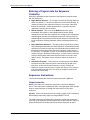
PAC-Designer Software
User Manual
Lattice Semiconductor Corporation
5555 NE Moore Court
Hillsboro, OR 97124
(503) 268-8000
July 2010
Copyright
Copyright © 2010 Lattice Semiconductor Corporation.
This document may not, in whole or part, be copied, photocopied,
reproduced, translated, or reduced to any electronic medium or machinereadable form without prior written consent from Lattice Semiconductor
Corporation.
Trademarks
Lattice Semiconductor Corporation, L Lattice Semiconductor Corporation
(logo), L (stylized), L (design), Lattice (design), LSC, CleanClock, E2CMOS,
Extreme Performance, FlashBAK, FlexiClock, flexiFlash, flexiMAC, flexiPCS,
FreedomChip, GAL, GDX, Generic Array Logic, HDL Explorer, IPexpress,
ISP, ispATE, ispClock, ispDOWNLOAD, ispGAL, ispGDS, ispGDX, ispGDXV,
ispGDX2, ispGENERATOR, ispJTAG, ispLEVER, ispLeverCORE, ispLSI,
ispMACH, ispPAC, ispTRACY, ispTURBO, ispVIRTUAL MACHINE, ispVM,
ispXP, ispXPGA, ispXPLD, Lattice Diamond, LatticeCORE, LatticeEC,
LatticeECP, LatticeECP-DSP, LatticeECP2, LatticeECP2M, LatticeECP3,
LatticeMico8, LatticeMico32, LatticeSC, LatticeSCM, LatticeXP, LatticeXP2,
MACH, MachXO, MACO, ORCA, PAC, PAC-Designer, PAL, Performance
Analyst, Platform Manager, ProcessorPM, PURESPEED, Reveal, Silicon
Forest, Speedlocked, Speed Locking, SuperBIG, SuperCOOL, SuperFAST,
SuperWIDE, sysCLOCK, sysCONFIG, sysDSP, sysHSI, sysI/O, sysMEM, The
Simple Machine for Complex Design, TransFR, UltraMOS, and specific
product designations are either registered trademarks or trademarks of
Lattice Semiconductor Corporation or its subsidiaries in the United States
and/or other countries. ISP, Bringing the Best Together, and More of the Best
are service marks of Lattice Semiconductor Corporation.
Other product names used in this publication are for identification purposes
only and may be trademarks of their respective companies.
Disclaimers
NO WARRANTIES: THE INFORMATION PROVIDED IN THIS DOCUMENT
IS “AS IS” WITHOUT ANY EXPRESS OR IMPLIED WARRANTY OF ANY
KIND INCLUDING WARRANTIES OF ACCURACY, COMPLETENESS,
MERCHANTABILITY, NONINFRINGEMENT OF INTELLECTUAL
PROPERTY, OR FITNESS FOR ANY PARTICULAR PURPOSE. IN NO
EVENT WILL LATTICE SEMICONDUCTOR CORPORATION (LSC) OR ITS
SUPPLIERS BE LIABLE FOR ANY DAMAGES WHATSOEVER (WHETHER
DIRECT, INDIRECT, SPECIAL, INCIDENTAL, OR CONSEQUENTIAL,
INCLUDING, WITHOUT LIMITATION, DAMAGES FOR LOSS OF PROFITS,
BUSINESS INTERRUPTION, OR LOSS OF INFORMATION) ARISING OUT
OF THE USE OF OR INABILITY TO USE THE INFORMATION PROVIDED
IN THIS DOCUMENT, EVEN IF LSC HAS BEEN ADVISED OF THE
POSSIBILITY OF SUCH DAMAGES. BECAUSE SOME JURISDICTIONS
PROHIBIT THE EXCLUSION OR LIMITATION OF CERTAIN LIABILITY,
SOME OF THE ABOVE LIMITATIONS MAY NOT APPLY TO YOU.
LSC may make changes to these materials, specifications, or information, or
to the products described herein, at any time without notice. LSC makes no
commitment to update this documentation. LSC reserves the right to
discontinue any product or service without notice and assumes no obligation
to correct any errors contained herein or to advise any user of this document
PAC-Designer Software User Manual
ii
of any correction if such be made. LSC recommends its customers obtain the
latest version of the relevant information to establish, before ordering, that the
information being relied upon is current.
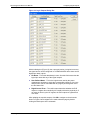
Type Conventions Used in This Document
Convention Meaning or Use
Bold
Items in the user interface that you select or click. Text that you type
into the user interface.
<Italic>
Variables in commands, code syntax, and path names.
Ctrl+L
Press the two keys at the same time.
Courier
Code examples. Messages, reports, and prompts from the software.
...
Omitted material in a line of code.
.
.
.
Omitted lines in code and report examples.
[ ]
Optional items in syntax descriptions. In bus specifications, the
brackets are required.
( )
Grouped items in syntax descriptions.
{ }
Repeatable items in syntax descriptions.
|
A choice between items in syntax descriptions.
PAC-Designer Software User Manual
iii
PAC-Designer Software User Manual
iv
Contents
PAC-Designer Software User Manual
Introduction
1
1
Creating/Opening a Design File
Configuring Analog Inputs
Configuring Digital Inputs
Configuring Digital Outputs
3
6
9
11
Configuring HVOUT Pins (MOSFET Driver Pins) 13
Configuring Timers
15
Implementing Power Management Algorithm in LogiBuilder
18
LogiBuilder - Sequence Control 19
Entering a Program into the Sequence Controller 20
Sequencer Instructions 20
LogiBuilder - Exception Conditions 39
Creating an Exception Condition 40
LogiBuilder - Supervisory Logic
43
Digital Timing Simulation Using PAC-Designer
Implementing Multiple State Machines
52
Creating a DC-DC Converter Library Entry
PAC-Designer Software User Manual
48
54
v
Contents
PAC-Designer Software User Manual
vi
PAC-Designer Software
User Manual
Introduction
Designs in any of the Power Manager devices can be implemented using the
PAC-Designer software tool. In addition, the PAC-Designer software provides
tools to simulate the power management design, download the design into a
device through parallel port or USB, and toggle registers in the device
dynamically during device operation. The PAC-Designer software can be
downloaded from the Lattice Web site free of charge.
Designing with the PAC-Designer software involves in the following main
steps:
1. Create/Open power management design
2. Configure analog input signals
3. Configure digital inputs
4. Configure digital output pins
5. Configure HVOUT pins (MOSFET driver outputs)
6. Configure Timer values
7. Configure I2C address
8. Implement power management algorithm using the LogiBuilder
9. Simulate the design and iterate through steps 2 through 6
10. Download the design into a Power Manager device and verify the design
When the PAC-Designer software is installed, the set-up utility also installs a
number of design examples. You can access these examples by choosing
File > Design Examples in the PAC-Designer software. Details of the design
examples are described in <pac-designer_install_path>\Examples\Design
Examples.ppt.
PAC-Designer Software User Manual
1
PAC-Designer Software User Manual
Introduction
The next sections will describe each of the designing steps in detail using the
following design example:
POWR1220AT8-2_cPCI_HS_Seq_RG_Sup.PAC – Complete board
power management for a CompactPCI add-on card.
The features of this design example are listed below:
Design: CompactPCI Board Power Management Including Hot-swap
±12V, 5V and 3.3V Hot-swap Controller (= LTC4245 IC)
Operate MOSFETs in Safe Operating Area (SOA)
Short Circuit Protection Individually On Each Supply Rail
Sequence Supplies: +12V, +5V, +3.3V & -12V (In That Order)
Protection Against Over Current Faults During Operation
Measure Voltage and Current Feed Individually on 12V, 5V & 3.3V
Supplies Through I2C
Interface to CompactPCI Backplane Logic Signals
Sequence On-Board DC-DC Converters
Monitor all Supplies for Faults & Generate Brown-out interrupt
Shut Down All Supplies in Reverse Order
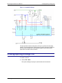
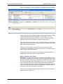
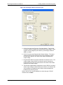
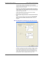
The power management block diagram is shown in Figure 1. Here the
ispPAC-POWR1220AT8 device is used to implement hot-swap, sequencing,
and reset generation functions.
PAC-Designer Software User Manual
2
PAC-Designer Software User Manual
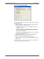
Creating/Opening a Design File
Figure 1: CompactPCI Design
The top left and the bottom left portions of Figure 1 performs the hot-swap
function. The top right portion of the diagram is used to sequence supplies on
the board and the right side of the diagram interfaces to the board reset,
supervision and other control functions.
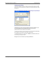
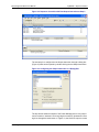
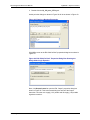
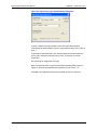
Creating/Opening a Design File
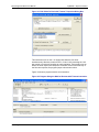
To create a new file:
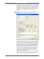
Choose File > New.
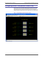
This opens a dialog box (Figure 2) that enables device selection.
PAC-Designer Software User Manual
3
PAC-Designer Software User Manual
Creating/Opening a Design File
Figure 2: Selecting a Device for a New Design
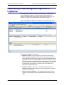
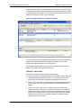
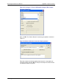
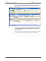
To open a file:
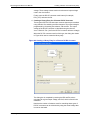
1. Choose File > Design Examples.
This opens the dialog box shown below in Figure 3.
Figure 3: Opening a Design Example
PAC-Designer Software User Manual
4
PAC-Designer Software User Manual
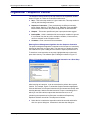
Creating/Opening a Design File
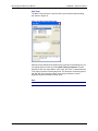
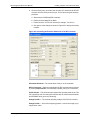
2. Select POWR1220AT8-2_cPCI_HS_Seq_RG_Sup.PAC and click Open
File.
The software opens the schematic page shown below in Figure 4.
Figure 4: CompactPCI Design in POWR1220AT8
PAC-Designer Software User Manual
5
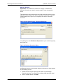
PAC-Designer Software User Manual
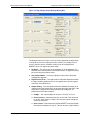
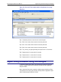
Configuring Analog Inputs
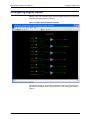
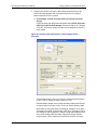
Configuring Analog Inputs
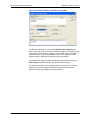
Analog inputs of the Power Manager device can be accessed by clicking the
Analog Inputs block shown at the top left corner of Figure 4 and the software
will open the schematic interface shown in Figure 5.
Figure 5: Analog Inputs Schematic Interface
This is the next level in the hierarchy that shows the comparators and the
associated voltage thresholds for each analog input. The outputs of the
comparator are connected to window logic and then to a glitch filter. The
output of the glitch filter is connected to the on-chip CPLD. The power
management algorithm is implemented in the CPLD.
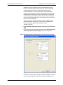
To configure the analog inputs, double-click any of the comparators to open
the dialog box shown in Figure 6.
PAC-Designer Software User Manual
6
PAC-Designer Software User Manual
Configuring Analog Inputs
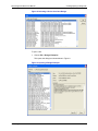
Figure 6: Analog Input Settings Dialog Box
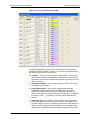
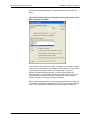
The following parameters of each of the analog inputs can be accessed
through the dialog box shown in Figure 6. (The names of these parameters
are shown on top of each of the columns.)
Pin Name – This is the name of the pin in the datasheet. This is a pulldown menu that enables associating any VMON pin to a schematic net.
This feature can be used to accommodate changes required by the layout
stage, for example.
Schematic Net Name – Enter the name of the schematic. This can be
any alphanumeric character.
Logical Signal Name – There are two programmable threshold
comparators associated with each of the VMON pins. The names
specified here will be used in the power management algorithm. All
names should begin with a letter. No spaces are allowed. To concatenate
two words, use the “_” (underscore). No other special characters are
allowed.
Monitoring Type – Over-Voltage / Under Voltage monitoring selection.
Each of the comparator can be used to monitor an over-voltage (OV) or
an under-voltage (UV) event. The difference between the OV and the UV
setting is location of hysteresis. For example, the OV comparator trips
exactly at the set threshold trip point when the voltage excursion is from
PAC-Designer Software User Manual
7
PAC-Designer Software User Manual
Configuring Analog Inputs
low to high. Once tripped, the voltage has to drop below the hysteresis
level to toggle the comparator back. If under voltage is set, then the
comparator trips during the input voltage high to low excursion and the
hysteresis is applied during the low to high excursion.
Trip Point Selection – This is a pull-down menu used to select the actual
trip point from a table of 368 trip points. The step size of these trip points
are spaced at 0.5% of the nominal voltage value that is monitored.
64 µs Glitch Filter – Each of the monitoring comparator can be
configured to ignore supply glitches narrower than 64 microseconds by
checking the associated box. This means that the output of the
comparator will transition only if the changed status remains active for a
period longer than 64 microseconds. If this box is not checked, then the
comparator output will toggle within 16 microseconds from the time the
voltage transitions through the appropriate trip point.
Window Mode – There are two comparators associated with each VMON
pin, Comparator A, and Comparator B. To use the window mode, the
Comparator B threshold should be lower than the threshold setting of
comparator A. The window mode output will replace the comparator A
output. The window output is logical high if the Comparator B output is
high and the Comparator A output is Low.
After entering the values into all required fields of the dialog box, click the OK
button to update the design and transition into the intermediate schematic
with two comparators per analog input (Figure 5). Position the cursor outside
the schematic region until the cursor becomes an up arrow. Click the left
mouse button to transition to the main schematic shown in Figure 4.
PAC-Designer Software User Manual
8
PAC-Designer Software User Manual
Configuring Digital Inputs
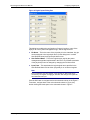
Configuring Digital Inputs
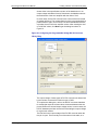
Starting at the main schematic page, click the Digital Inputs block to open the
secondary schematic shown in Figure 7.
Figure 7: Digital Inputs Schematic Interface
This diagram shows six input buffers receiving the input from the input pin or
the internal I2C register. Click any input buffer to open a dialog box shown in
Figure 8.
PAC-Designer Software User Manual
9
PAC-Designer Software User Manual
Configuring Digital Inputs
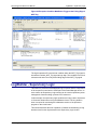
Figure 8: Digital Inputs Dialog Box
This dialog box enables the configuration of input pin location, name of the
input pin for use in power management logic, and the signal source.
Pin Name – This is the name of the physical pin in the datasheet. Any pin
can be assigned to the logical pin name (in this dialog box it is called
User-Defined Name) through the pull-down menu.
User-Defined Name – This is the logical name used by the power
management algorithm implemented in the CPLD. The default association
of the physical pin can be changed by changing the Pin Name field.
Input From – This associates the logical signal name specified in the
User-Defined Name field to either a physical pin or an internal register.
Note
IN1 is controlled by the JTAG register or the external pin. IN2 to IN6 can be
controlled by I2C register. Changing pin allocation also changes the register bit
associated with that input.
Click the OK button to navigate back to the schematic shown in the Figure 7.
From there, navigate back to the main schematic shown in Figure 4 by
double-clicking the blank space in the schematic shown in Figure 7.
PAC-Designer Software User Manual
10
PAC-Designer Software User Manual
Configuring Digital Outputs
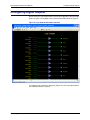
Configuring Digital Outputs
Double-click the Logic Outputs block on the bottom right side of the schematic
shown in Figure 4 to navigate to the next level schematic shown in Figure 9.
Figure 9: Logic Outputs Schematic Interface
To configure logic outputs in a dialog box (Figure 10), click any output buffer in
the schematic shown in Figure 9.
PAC-Designer Software User Manual
11
PAC-Designer Software User Manual
Configuring Digital Outputs
Figure 10: Logic Outputs Dialog Box
With this dialog box (Figure 10), the output pin location, its logical name and
the signal source can be configured. In a POWR1220AT8 device there are 20
digital open drain outputs.
Pin Name – This is the datasheet pin name. Use this field to associate the
logical pin name with any of the logical outputs.
User-Defined Name – This is the logical name used by the power
management algorithm to toggle the corresponding output pin. Any userdefined name can be associated with any logical pin through the use of
the Pin Name field.
Digital Control From – The radio buttons determine whether the PLD
output or a register bit controlled by I2C interface drives the physical pin. If
an output is driven by the I2C register, the PLD outputs are ignored and
vice versa.
After updating the requisite outputs, click OK to navigate to the schematic
shown in Figure 9 and navigate to the main schematic page by doubleclicking the blank space in the schematic.
PAC-Designer Software User Manual
12
PAC-Designer Software User Manual
Configuring HVOUT Pins (MOSFET Driver Pins)
Configuring HVOUT Pins (MOSFET Driver Pins)
Double-click the block called High Voltage Outputs located above the Logic
Outputs block to navigate into an intermediate schematic that shows FET
driver blocks (Figure 11). Double-click any FET Driver block to navigate to the
dialog box (Figure 12) that can be used to configure each of the HVOUT pins.
Figure 11: High Voltage Outputs Schematic Interface
PAC-Designer Software User Manual
13
PAC-Designer Software User Manual
Configuring HVOUT Pins (MOSFET Driver Pins)
Figure 12: High Voltage Output Settings Dialog Box
The dialog box shown in Figure 12 can be used to associate the physical pin
to a logical pin name, the output pin control, HVOUT pin’s voltage, source
current, and sink current. In addition, each pin can be configured as a
MOSFET driver or a logical open drain output.
Pin Name – This is the name of the hardware pin in the datasheet. To
associate this pin with a different user-defined name, change the HVOUT
pin name using the pull-down menu.
User-Defined Name – This is the logical pin name used in the power
management algorithm
Digital Control From – The radio buttons in this field determine whether
the logic equations within the PLD or the register bits in the I2C register
control the actual HVOUT pin.
Output Setting – The radio buttons determine whether the output pin is
configured as a high voltage pin or as an open drain logic output pin. If the
output pin is configured as a charge pumped high voltage pin, its
properties can be further changed:
Voltage – The output voltage can be set to 12V, 10V, 8V, or 6V.
Source Current – Determines the turn on slew rate. This can be set
to 12.5µA, 25µA, 50µA, or 100µA. The lower the current setting, the
slower the ramp rate.
Sink Current – Determines how fast the MOSFET is turned off when
the output pin switches to Logic ‘0’. This can be set to 100µA, 250µA,
PAC-Designer Software User Manual
14
PAC-Designer Software User Manual
Configuring Timers
500µA, or 3000µA. The higher the current, the faster the MOSFET
turn-off process.
Click OK to jump to the intermediate schematic (Figure 11) and double-click
the blank space to navigate to the main schematic (Figure 4).
Configuring Timers
The power management algorithm requires long duration timers. The Power
Manager device implements four hardware timers which can be configured
independently. Double-click the Timer block in between the Logic Outputs
block and the Logic Inputs block at the bottom to navigate to an intermediate
schematic shown in Figure 13.
Figure 13: Clock & Timers Schematic Interface
The above figure shows four timers and the clock source. Double-click any
Timer block to navigate to Clocks & Timers dialog box shown in Figure 14.
PAC-Designer Software User Manual
15
PAC-Designer Software User Manual
Configuring Timers
Figure 14: Clocks & Timers Dialog Box
The Clocks & Timers dialog box can be used to configure three sections of the
Power Manager device.
Master Clock Source – Configures the device as a standalone, master,
or a slave by selecting the radio button options:
Standalone – Runs the device on its internal 8MHz oscillator. The
MCLK pin is tristated.
Master – In this state this Power Manager device is a master and
sources the main 8MHz clock for all the devices. The clock source is
still its internal 8 MHz oscillator.
Slave – This mode enables the Power Manager device to receive the
clock sourced from another master.
PLD Buffered Clock Output – This radio button setting determines
whether the 250KHz clock output pin is tristated or not.
Timers – This section enables time delay setting between 32
microseconds to 2 seconds (122 steps) for each of the timer through the
pull-down menu.
Click OK to update the configuration and transition to the main schematic via
the intermediate schematic shown on Figure 13.
PAC-Designer Software User Manual
16
PAC-Designer Software User Manual
Configuring Timers
Configuring the I2C Block
In the main schematic (Figure 4), double-click the I2C block above the ADC
block at the top of the schematic to navigate to the following dialog box shown
in Figure 15.
Figure 15: Configuring the I2C Address & Controlling the Inputs/Outputs
This dialog box is used to set the I2C address of the device between 0 and
7E. The I2C address is then programmed into the device and the
PWOR1220AT8 device responds to that address.
The Input and output pin control through I2C can also be set from this dialog
box in addition to the input and output block dialog boxes.
The POWR1220AT8 device supports the SMBAlert mechanism and this can
be enabled by selecting the option.
Navigate to the main schematic by clicking the OK button.
PAC-Designer Software User Manual
17
PAC-Designer Software User Manual
Implementing Power Management Algorithm in LogiBuilder
Implementing Power Management Algorithm in
LogiBuilder
After configuring all inputs and outputs, the next step is to implement the
power management algorithm. For that, begin by double-clicking the
Sequence Controller block at the middle of the schematic (Figure 4). The
software navigates to the LogiBuilder window shown in Figure 16.
Figure 16: LogiBuilder Window for Sequence and Supervisory Logic
This window is divided into 3 sections:
Sequence Control – Enter a sequence of events and actions in the
power management algorithm. There can be more than one sequence
control algorithms. Each of these sequence control algorithms executes in
parallel. The sequence control algorithm is made up of a number of steps.
Each of these steps contains an instruction. The sequence control engine
executes each of the instructions using the 250KHz PLD clock. Some of
the instructions get executed in one clock cycle or 4us while some
instructions require many cycles.
Exception Control – This can be considered as an interrupt to the
sequence control flow. Each sequence control algorithm has a separate
Exception Control section.
Supervisory Logic Equation – This enables implementation of logic
made up of equation that can run in parallel with the sequence control
logic.
PAC-Designer Software User Manual
18
PAC-Designer Software User Manual
LogiBuilder - Sequence Control
LogiBuilder - Sequence Control
The Sequence Control section is the top window of the LogiBuilder window
shown in Figure 16. There are 5 columns in this section:
Step – This is the step number of a given instruction. This step number is
used by the branching instructions.
Sequencer Instruction – There are basically six different instruction
types: Output, Wait for, If-Then-Else, Go to, Start/Stop Timer, and NOP.
Each of these instructions along with its application is described later.
Outputs – This section specifies only the output pins that are toggled.
Interruptible – If this is marked as No, the exception condition is ignored.
If it is marked Yes, then any of the exception condition, if becomes true,
can force a branch to the exception routine.
Comment – Enter comment for documentation.
Entering Power Management Algorithm into the Sequence Controller
The power management algorithm is entered into the Sequence Controller by
inserting an instruction at a given step. The next step is to double-click that
new instruction to open a dialog box and enter the required parameters in it.
To introduce a new instruction at any step, highlight that step number and
press the Insert key. The software opens a dialog box shown in Figure 17.
Figure 17: Inserting a New Sequence Control Instruction at a Given Step
After inserting an instruction, it can be customized to perform the required
function. For example, Figure 17 shows the Outputs instruction highlighted.
Click the OK button, this outputs instruction will get inserted at that step. After
inserting that step, double-click that instruction to open a new dialog box in
which you can select all the outputs that should be turned on or off.
Introducing the expressions into Exception condition and Supervisory
Equations sections are similar. The steps are as follows:
Select the line on which the expression should be entered and doubleclick it to open a dialog box. Customize it and close the dialog box.
PAC-Designer Software User Manual
19
PAC-Designer Software User Manual
LogiBuilder - Sequence Control
Entering a Program into the Sequence
Controller
When the LogiBuilder window is launched, the Sequence Controller starts
with four instructions:
Begin Startup Sequence – The sequencer enters the first step when the
device is powered on. The first time when the control enters this step, all
outputs are reset to their respective power-on reset values. Other than
that this is essentially a marker step and does not perform any other
useful task. This step can be deleted.
Wait for AGOOD – This is one of the Wait for instruction types.
Immediately after power-on, the PWOR1220AT8 initiates analog
calibration process. After the completion, the analog section activates the
AGOOD signal internally. All comparator outputs are valid only after the
AGOOD signal is at logic HIGH. In this step the Sequence Controller waits
for the completion of analog calibration before proceeding with the next
steps.
Begin Shut Down Sequence – This step performs two functions: marker
step indicating that the power shut down sequence is found after that step
and when you double-click this step, it automatically allows insertion of an
instruction into that step and the shut down sequence marker moves to
the next step. For example, in Figure 16, the Begin Shut Down sequence
marker is at step 2. By double-clicking step 2, you can insert an instruction
at step 2 and the Begin Shut Down sequence marker moves one step
down to step 3. This marker can be deleted to reduce the number of
steps.
Halt (End of Program) – This instruction is a special case of the Go to
instruction where the sequence jumps to the same step as that of the
instruction. In this case the Halt instruction is at step 3. When the
Sequence Control enters this step, it stays at this step for ever. However,
if the Interruptible flag was set to Yes, then an exception condition can
transfer it to another step.
Sequencer Instructions
This section describes the instructions supported by the LogiBuilder.
Output Instruction
Action: This instruction controls the output pins of the Power Manager
device. The output status is maintained until it is changed again either through
another output instruction or through the output section of any other
instruction.
Purpose: This is used functions such as turning a supply on/off or activating/
deactivating a supervisory signal or turning a MOSFET on/off.
The Output instruction is inserted into a sequence control step through the
Insert key on the keyboard and selecting the raw Output instruction. Figure 18
shows the Sequence Controller with the raw Output instruction at step 2.
PAC-Designer Software User Manual
20
PAC-Designer Software User Manual
LogiBuilder - Sequence Control
Figure 18: Sequence Controller with Raw Output Instruction at Step 2
The next step is to configure the raw Output instruction through a dialog box
(Figure 19) that can be opened by double-clicking the raw Output instruction.
Figure 19: Configuring the Output Instruction in a Dialog Box
The top window shows all outputs of the Power Manager device. Any output
can be turned on / asserted / set to logic high or turned off / deasserted / set to
logic low through the radio button. In Figure 19, the HVOUT2 output is turned
PAC-Designer Software User Manual
21
PAC-Designer Software User Manual
LogiBuilder - Sequence Control
on and the OUT5 output is turned off. When the OK button is clicked, the step
2 of the sequence control output is changed to show (Figure 20) the operation
on HVOUT2 and OUT5 signals. There is no limit to the number of instructions
that can be turned on or off in a given instruction.
Figure 20: Output Instruction Configured at Step 2
The check box next to the exceptions can be checked to indicate whether this
instruction can be interrupted by the exception condition or not. In this
example, the output instruction can be interrupted.
The Comment section can store any text that will appear in the Comment
section of the Sequence Controller at that step.
“Wait for” Instruction
The “Wait for” instruction type includes three sub types.
Wait for <Boolean> – Causes the sequence controller to stall at that step
until the Boolean expression becomes true. The Sequence Controller
jumps to the next step after the Boolean expression becomes true.
Wait for <Timeout Value> – Starts the timer and waits at that step until the
timer expires. The Controller proceeds to the next step after the timer
expires.
Wait for <Boolean> with Timeout – Starts the timer and waits for the
Boolean condition to become true until the timer expires. If the Boolean
condition becomes true within that time period, the Sequence Controller
jumps to the next step. However, if the timer expires before the Boolean
expression becomes true, the Controller jumps to a different location
determined by the instruction.
PAC-Designer Software User Manual
22
PAC-Designer Software User Manual
LogiBuilder - Sequence Control
Wait for <Boolean>
Application: This instruction is used to turn a supply on and hold the
Sequence Controller at a step for a power supply to reach its regulation
levels.
This instruction is first inserted as raw into a step using the Insert key on the
keyboard. Double-click the raw “Wait for <Boolean>” instruction to open the
following dialog box (Figure 21) for configuring the “Wait for <Boolean>”
instruction.
Figure 21: Edit “Wait For Bool” Properties Dialog Box
In the dialog box, click Edit Boolean Expression to open the following dialog
box (Figure 22).
Figure 22: Boolean Expression Editor
Any Boolean function can be created using any of the input or output signals
by the following process.
1. Double-click the required input signal to transfer it to the Boolean
Expression window. First, double-click the Core_1V2_over_LTP signal.
2. Click an operator button. Click AND.
PAC-Designer Software User Manual
23
PAC-Designer Software User Manual
LogiBuilder - Sequence Control
3. Double-click the IO_1V8_over_LTP signal.
At this point the dialog box shown in Figure 22 will be as shown in Figure 23.
Figure 23: Entering a Boolean Expression
Click OK to return to the Edit “Wait for Bool” properties dialog box as shown in
Figure 24.
Figure 24: Edit “Wait For Bool” Properties Dialog Box Showing the
Newly-Added Logic Equation
Next, click Output Control to open the Edit “Output” properties dialog box
shown in Figure 25. This is the same dialog box as that of the Output
instruction. Here the core supply (1.2V) enable and IO supply (1.8V) enable
signal are turned on.
PAC-Designer Software User Manual
24
PAC-Designer Software User Manual
LogiBuilder - Sequence Control
Figure 25: Turning on 1.2V and 1.8V Supplies Using the Edit “Output”
Properties Dialog Box
Next, click OK. The “Wait for Boolean” instruction gets updated, as shown in
Figure 26.
Figure 26: Wait for <Boolean> Instruction Getting Updated
Enter the comment and indicate whether this instruction is interruptible via
exception condition and click OK. The Step 3 in the Sequence Control section
is modified as shown in Figure 27.
PAC-Designer Software User Manual
25
PAC-Designer Software User Manual
LogiBuilder - Sequence Control
Figure 27: Sequence Control Section Showing the Updated “Wait for
<Boolean>” Instruction
When the Sequence Controller executes step 3, it first turns on core supply
(1.2V) and IO supply (1.8V) and waits until the output voltages of both
supplies reach the regulation levels.
Wait for <Timeout Value>
Application: This instruction is used for functions such as: wait a certain
period for a supply to stabilize after turn on or time based sequencing or to
extend the reset pulse after all supplies are turned on.
This instruction is edited by using the following dialog box shown in Figure 28.
PAC-Designer Software User Manual
26
PAC-Designer Software User Manual
LogiBuilder - Sequence Control
Figure 28: Edit “Wait for Timeout” Properties Dialog Box
The first step is to select the timer used for implementing the timeout delay. It
is possible to change the value of the time delay from this dialog box by
clicking Edit Timeout properties to go to the Clocks & Timers dialog box
shown in Figure 14. It is possible to enable outputs along with this step. For
example, in Figure 29, the Timer 1 (5.12ms duration) is started and the 1.2V
core supply is also turned on. The Sequence Controller waits in that step till
the Timer 1 expires.
Figure 29: Wait for Timeout to Turn on the Supply & Wait for 5.12ms
By clicking OK and adding another “Wait for timeout” instruction and an
Output instruction, the Sequence Controller program is shown in Figure 30.
PAC-Designer Software User Manual
27
PAC-Designer Software User Manual
LogiBuilder - Sequence Control
Figure 30: Program to Turn on Supplies in a Sequence & Release Reset
At step 1, the Sequence Controller is waiting for the AGOOD signal (or waiting
for the completion of the analog calibration). While waiting, 1.2V, 1.8V
supplies are turned off and the reset to CPU is active. When the AGOOD
signal becomes active, the Sequence Controller jumps to step 2.
As soon as the code enters step 2, the 1.2V supply is turned on and the 5ms
timer (Timer 1) is also turned on. The Sequence Controller waits until the 5ms
timer expires and jumps to step 3.
At step 3, the 1.8V supply is turned on and Timer 2 (200ms) is started
simultaneously. The Sequence Controller waits at step 3 for 200ms (until the
timer 2 expires) and jumps to step 4.
At step 4, the CPU reset is released. The Sequence Controller transitions
through step 5 without any action and stops at step 6.
Wait for <Boolean> with Timeout
Application: The Wait for Boolean instruction waits for the Boolean function
to become true indefinitely. For example, if a power supply fails to turn on, the
Sequence Controller can be stuck at that Wait for Boolean instruction. Some
devices cannot withstand being left partially turned on for a very long period of
time. To deal with such cases, Wait for Boolean with Timeout instruction is
used. This instruction turns on a supply and waits for a fixed period of time for
it to turn on. If the supply fails to turn on, the Sequence Controller times out
and jumps to shut down that section of the design.
This instruction is edited by the Edit “Wait For Bool with Timeout” properties
dialog box shown in Figure 31.
PAC-Designer Software User Manual
28
PAC-Designer Software User Manual
LogiBuilder - Sequence Control
Figure 31: Edit “Wait For Bool with Timeout” Properties Dialog Box
This instruction turns on the 1.2V supply and starts the 5ms timer
simultaneously. After that, it waits for the 1.2V and 1.8V (assuming the 1.8V
was turned on previously) supplies to reach regulation. If the supply turns on
before the timer expires, the Sequence Controller moves to the next step. If
the 5ms timer expires, the program jumps to shut down routine.
Figure 32 shows a program with this new instruction.
Figure 32: Program Using the Wait for Boolean with Timeout Instruction
PAC-Designer Software User Manual
29
PAC-Designer Software User Manual
LogiBuilder - Sequence Control
At step 1, the program waits for the calibration process to complete with all
supplies tuned off.
At step 2, the 1.8V supply is turned on and simultaneously the Timer 1 (5ms)
is also started. The Sequence Controller waits at step 2 for 5ms after turning
on the 1.8V supply and jumps to Step 3.
At step 3, the 1.2V supply is turned on and simultaneously the Timer 1 is
restarted. The Sequence Controller waits for the 1.8V and 1.2V supplies to
reach regulation within 5ms. If both supplies reach regulation within 5ms, the
Sequence Controller jumps to step 4, where it waits for 200ms and jumps to
step 5. At step 5, the Sequence Controller halts with the reset signal released.
The sequence error flag is cleared. The circuit board functions normally.
However, at step 3, if the supplies did not reach regulation levels before 5ms,
the step times out and jumps to step 6 to begin the shutdown operation. The
code jumps to step 7.
At step 7, both the supplies are turned off and the Seq_err flag is turned on
indicating that the board failed to sequence.
“Start/Stop Timer” Instruction
Application: The previously described “Wait for Timeout” instruction starts
the timer and waits for it to expire in that same step. In some cases, you may
want to just start the timer at one step and check on it at a completely different
step. For example, you can implement a watchdog timer function where a
timer is started at one of the steps and the sequence control can monitor for
timer expiry at a different step while performing different functions.
There are 2 sub types of timer control instructions:
PAC-Designer Software User Manual
30
PAC-Designer Software User Manual
LogiBuilder - Sequence Control
Start Timer
The Start Timer instruction is used to start a given timer through the dialog
box shown in Figure 33.
Figure 33: Start Timer Dialog Box
Select the timer that should be started in the top section of the dialog box. you
can change the timer value by clicking Edit Timeout properties. It is also
possible to alter any output status. In this case, the Timer 1 is started and the
1.2V supply is turned on at the same time. The Sequence Controller jumps to
the next step. Re-execution of Start Timer during a sequence control
algorithm stops and restarts the same timer.
Note
The Stop Timer instruction step cannot be a target of branch instruction.
PAC-Designer Software User Manual
31
PAC-Designer Software User Manual
LogiBuilder - Sequence Control
Stop Timer
The Stop Timer instruction stops the timer. It can be configured using the
following dialog box. (Figure 34)
Figure 34: Stop/Reset Timer Dialog Box
“If-Then-Else” Instruction
There are 2 types of If-Then-Else instructions.
If-Then-Else – This instruction checks for a Boolean expression. If it is
true, it goes to the step indicated by the Then section. If the Boolean
expression is false, it jumps to a different branch indicated by the Else
section. This instruction is used to control the flow of the sequence control
program. Along with that this instruction can also activate different outputs
depending the Boolean logic status.
If-Then-Else with Timeout – This instruction, in addition to functioning like
the instruction above, checks on a timer expiry and provides a third
branch address with another output control section.
If-Then-Else
Application: This instruction can be used to poll different inputs and perform
different functions depending on the inputs. For example, the Sequence
Controller can monitor supply voltages and branch to shut down routine and
poll for an input condition, and jump back to monitor voltages.
The If-Then-Else instruction can be configured using the dialog box shown in
Figure 35.
PAC-Designer Software User Manual
32
PAC-Designer Software User Manual
LogiBuilder - Sequence Control
Figure 35: Conditional Branch (IfThenElse) Dialog Box
The Boolean expression is set by clicking Edit Boolean Expression as
shown in the Figure 23. In this case the sequence engine is monitoring for the
core voltage of 1.2V and the IO supply of 1.8V. If either supply is faulty, the
sequence control jumps to the shutdown section of the sequence control
program (step 6). Otherwise it jumps to the next step (step 4).
It is possible to change any output during the branch transition by clicking
with Outputs associated with the Then and the Else branches.
The following sequence control program (Figure 36) uses two If Then Else
instructions to poll the supply fault and input reset signal and performs
different functions depending on the input conditions.
PAC-Designer Software User Manual
33
PAC-Designer Software User Manual
LogiBuilder - Sequence Control
Figure 36: Sequence Controller Polling Digital Input and Supply Fault
Step 1 – The sequence control program waits for the analog calibration.
Step 2 – Both 1.2 and 1.8V supplies are turned on and the program waits for
5ms.
Step 3 – If the supplies are faulty, jumps to the shutdown program, turns off
both supplies, flags error and goes to halt. If the supplies are OK, then jumps
to step 4.
Step 4 – If the Reset_in signal is at logic 1 then Reset_CPU = logic 1 else,
Reset_CPU signal = Logic 0.
If-Then-Else with Timeout
Application: (This instruction assumes that the timer is started beforehand
using the Start Timer instruction). This instruction is used to monitor a number
of events with one watchdog timer. For example, in a circuit board a number
of supplies can be turned on and these supplies should all be stable within a
certain period of time. If they fail to turn on, the shutdown function is initiated.
This instruction can also be used to implement a watchdog timer in a system.
The If-Then-Else with Timeout instruction can be configured using the
following dialog box (Figure 37).
PAC-Designer Software User Manual
34
PAC-Designer Software User Manual
LogiBuilder - Sequence Control
Figure 37: Edit “IfThenElse with Timeout” Properties Dialog Box
The test Boolean function along with the outputs to be toggled during the step
is entered as described from Figure 21 to Figure 24.
The instruction first tests the Boolean condition to be true. If the Boolean
condition is true, then it branches to the step indicated by the pull-down menu
next to “On Condition Go to Sequencer step”.
If the Boolean condition is false, the instruction tests the timer expiry. If the
timer has expired, the Sequence Controller branches to the step indicated by
the pull-down menu next to “On Timeout Goto Sequencer step”.
If the timer has not expired, the Sequence Controller branches to the step
selected by the pull-down menu next to “Else Goto Sequencer step”.
Each branch condition can be set to toggle different sets of outputs
independently through the Output Control button.
The following sequence control program (Figure 38) uses the If-Then-Else
with Timeout instruction.
PAC-Designer Software User Manual
35
PAC-Designer Software User Manual
LogiBuilder - Sequence Control
Figure 38: Using If-Then-Else with Timeout in a Hot-Swap Application
When a circuit board is plugged into a backplane, during initial stages of
contact there will be a contact bounce. The backplane has two supplies: 3.3V
and 5V. During the contact bounce period, the 5V and 3.3V supplies will be
intermittent. This routine waits until the contact bounce settles and then
proceeds with the hot-swap event.
Step 0 – Marker.
Step 1 – Waits for the calibration.
Step 2 – Initialization of various outputs.
Step 3 – 100ms timer is started using the Start Timer instruction.
Step 4 – The If-Then-Else with Timeout instruction checks to see if the 5V and
3.3V supplies are within limits. If not, the program jumps to restart the timer.
(Notice that the program branches to a step previous to that of the Start Timer
instruction). If the supplies are within tolerance, the code waits at the same
step until the timer expires. When the timer expires, the code jumps to the
next step. This instruction ensures that the backplane voltage is continuously
on for 100ms before jumping to the hot-swap portion of the code.
PAC-Designer Software User Manual
36
PAC-Designer Software User Manual
LogiBuilder - Sequence Control
“Go to” Instruction
This is a branch control instruction. The target jump location can be specified
using the dialog box shown in Figure 39.
Figure 39: Edit “Goto” Instruction Properties Dialog Box
The target Goto step can be set using the Step number pull-down menu. You
can set the outputs also along with this instruction.
“NOP” Instruction
The NOP instruction basically does nothing. This instruction is necessary to
enable a branch to terminate in a step previous to a timer control instruction,
such as the Wait For Timeout, Start/Stop Timer, or If-Then-Else with Timeout
instructions.
Figure 40: Watchdog Timer Implementation
PAC-Designer Software User Manual
37
PAC-Designer Software User Manual
LogiBuilder - Sequence Control
Step 0 – No action.
Step 1 – Waits for the calibration to complete and sets the watchdog timer
output to logic 1.
Step 2 – NOP does nothing.
Step 3 – Starts a 500ms timer.
Step 4 – If WDT_Trig signal is 0, restarts the 500ms timer. If the timer expires,
sets the interrupt to logic 0 and restarts the timer. If the WDT_Trig signal is at
logic high, waits at the same step until the trigger reaches 0 or the timer
expires.
As you see, the NOP instruction provides a method to restart the timer by
overcoming the limitation of no direct jump allowed to a timer control
instruction.
“Halt” Instruction
The Halt instruction stops the execution of the sequence. The last Halt
instruction is normally prevented to preserve a fail-safe stopping point for a
sequence. In cases where sequence flow is controlled by other means, the
last Halt instruction in the sequence window can be deleted. You can enable
the deletion of the last halt instruction by choosing Options > LogiBuilder
Options in a LogiBuilder window (Figure 41). The following dialog box will
open.
Figure 41: Allowing Deletion of the Last Halt Instruction
Select the “Allow deletion of the last Halt instruction” option and you will no
longer be prevented from deleting any Halt instruction.
PAC-Designer Software User Manual
38
PAC-Designer Software User Manual
LogiBuilder - Exception Conditions
LogiBuilder - Exception Conditions
So far the sequence control window of the LogiBuilder was described. The
next section of the LogiBuilder window is Exception Condition. Exception
conditions are used to interrupt the Sequence Controller flow to enable the
sequence control program to respond differently to an external stimulus
without looking for it in the main sequence code. The Exception Condition
section of the LogiBuilder window is shown in the Figure 42.
To show the use of the exception conditions, the watchdog timer design in
Figure 40 is modified to monitor for supply failure while monitoring for
watchdog timer, as shown in Figure 42.
Figure 42: Exception Condition Section in LogiBuilder
The sequence control in Figure 42 is as follows:
Step 0 – Start up marker.
Step 1 – Waits for the calibration with all supplies turned off and with reset
CPU active.
Step 2 – Turns on the 1.2V and 1.8V supplies and waits for them to reach
regulation levels.
PAC-Designer Software User Manual
39
PAC-Designer Software User Manual
LogiBuilder - Exception Conditions
Step 3 – Waits for 200ms.
Step 4 – Releases CPU reset to complete the reset pulse stretch function.
Step 5 – Starts/Restarts the 500ms watchdog timer.
Step 6 – Monitors for failure of the 1.2V and 1.8V supplies as well as
watchdog timer fault. If a power supply fault is detected, the Sequence
Controller jumps to shut down with the reset activated. If the watchdog timer
expired, toggles the WDT_Intr output signal, jumps back to step 4, restates
the watchdog timer at step 5, and resumes fault monitoring at step 6.
So how the watchdog timer is re-triggered?
This is handled by the exception condition. The step 6 has the interruptible
flag enabled. This means that the exception condition can interrupt the
sequence control flow. The watchdog trigger input is being monitored by the
exception condition E0.
The E0 is monitoring for a low going pulse of the watchdog timer. When it
happens, the sequence control program is forced to jump to step 4 (the step
before the restart of watchdog timer) and the code restarts the time in step 5
and jumps to step 6 to resume monitoring for voltage fault and the expiration
of the watchdog timer.
Creating an Exception Condition
To create an exception condition, double-click <end of exception-table> or
select the end of exception table and press the Insert key.
The LogiBuilder inserts a raw exception condition as shown in Figure 43.
Figure 43: Exception Condition Fresh Entry: E0
PAC-Designer Software User Manual
40
PAC-Designer Software User Manual
LogiBuilder - Exception Conditions
To configure the exception condition, double-click E0 and edit the dialog box
as shown in Figure 44.
Figure 44: Exception Properties Dialog Box
The first step is to enter the exception condition Boolean equation. To do this,
click Edit on the top section of the dialog box to open the Boolean expression
builder shown in Figure 23.
The next step is to identify the step that the Sequence Controller should jump
to when the Boolean condition becomes true.
It is possible to toggle an output during the exception condition. The output
value can be changed asynchronously (similar to activating the asynchronous
set or reset of a D flip-flop) or synchronously (similar to changing the D-input
of the D flip-flop). The next example shows how the output control can be
used in a design.
In the example shown in Figure 42, the exception condition looked into a low
going signal of watchdog trigger input. This design has one problem. If the
processor hung with the WDT_Trig stuck at logic 0, the watchdog trigger
mechanism does not recover. For that the exception condition is modified to
trigger only on the falling edge of the WDT_Trig input in its logic equation.
To capture the falling edge of the WDT-Trig signal, a second exception
condition is used. The second exception condition latches the trigger signal
into another register Latch_Wdt_Trig (an internal node. The procedure to
creating an internal node is described later in this section). Figure 45 shows
PAC-Designer Software User Manual
41
PAC-Designer Software User Manual
LogiBuilder - Exception Conditions
the Exception properties dialog box to implement latching of the WDT-Trig
signal.
Figure 45: Exception Properties Dialog Box Showing the Latching of the
WDT-Trig Signal into a Node
In this figure the logic expression is WDT_Trig signal. The exception condition
location is not used as there is no exception function specified. In the outputs
controlled by the expression section, the Latched_WDT_Trig node is
selected. The selected logical operator is “Synchronously follows the
expression (D-FF)”. This operation converts the Latched_WDT_Trig into a DFF with its data connected to the WDT-Trig signal and is clocked by the
250kHz clock that is clocking the Sequence Controller.
Now the original logic expression in the exception logic E0 shown in Figure 42
is modified to recognize the falling edge of the WDT_Trig signal instead of just
logic 0. Figure 46 shows the modified logic in the exception condition E0.
PAC-Designer Software User Manual
42
PAC-Designer Software User Manual
LogiBuilder - Supervisory Logic
Figure 46: Exception Condition Modified to Trigger at the Falling Edge of
WDT-Trig
The logic expression E0 now looks at condition when the WDT_Trig signal is
low and the Latched_WDT_Trig signal at logic high. This condition is true for 4
microseconds and occurs only at the falling edge of the WDT_Trig signal.
LogiBuilder - Supervisory Logic
This section is provided to add additional logic functions that are independent
of the sequence control into the CPLD part of the Power Manager device. In
some cases, the Supervisory Logic section can be used to implement power
management functions taking up fewer CPLD resources.
In this example, the supervisory logic equations are being used to implement
a 10 second duration timer using the hardware timers. This long duration
timer is required for monitoring the initialization section of the processor
program on the circuit board.
This section describes the timer operation to facilitate understanding of long
duration timer function implemented in the Supervisory Logic section.
PAC-Designer Software User Manual
43
PAC-Designer Software User Manual
LogiBuilder - Supervisory Logic
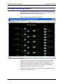
Hardware Timer Architecture Implemented in Power Manager Device
When Timer_gate is at logic high, the hardware timer in the Power Manger
counts down from a preloaded value (programmable from 32us to 2 seconds)
to 0 and generates a Logic 1 on the Timer_TC signal as shown in Figure 47.
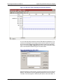
Figure 47: Power Manager Timer Operation
If the gate signal toggles to zero while the timer is counting down, the timer
delay value gets reloaded and the count down restarts.
There is a special mode of operation of the timer where the timer gate is
connected to an inverted Timer TC signal. In this case, the timer TC signal
generates a 4 microsecond pulse train separated by the time delay
programmed into the Timer (in this case it is 2 seconds). The connection and
the output waveforms are shown in Figure 48.
Figure 48: Generating a Train of Pulses 4us Wide and Separated by 2
Seconds
PAC-Designer Software User Manual
44
PAC-Designer Software User Manual
LogiBuilder - Supervisory Logic
Ten-Second Timer Implementation Using the Supervisory Logic Section
Refer to Figure 49. To insert a new supervisory equation, EQ0, double-click
<end-of-supervisory-logic-table> or place the cursor on the last line in the
Supervisory Logic window and press the Insert key.
Figure 49: Supervisory Logic Section in LogiBuilder
The supervisory equation representation is divided into 4 parts: the equation
number (automatically generated), the logic equation (a Boolean expression
assigned to an output pin or node), type of assignment (Combinatorial, Dtype, T-Type, Asynchronous Preset, and Asynchronous Reset), and a
comment line for documentation.
To enter the actual supervisory logic equation, double-click the newly
introduced supervisory equation to open the dialog box shown in Figure 50.
PAC-Designer Software User Manual
45
PAC-Designer Software User Manual
LogiBuilder - Supervisory Logic
Figure 50: Supervisory Logic Equation Entry Dialog Box
To enter a supervisory logic equation, select the output that should be
controlled by the logic equation. Here the output selected is the Timer_Gate of
timer 1.
To generate a pulse train that is 4us wide and spaces 2 seconds apart, the
Timer_Gate1 should be connected to its Timer_TC through an inverter
(Figure 48).
So, select type of assignment as D-type.
Next, click the Edit button to open the Boolean Expression Editor shown in
Figure 22. Here the assigned Boolean expression is Not Timer1_TC.
Click OK. The LogiBuilder window gets updated as shown in Figure 51.
PAC-Designer Software User Manual
46
PAC-Designer Software User Manual
LogiBuilder - Supervisory Logic
Figure 51: Supervisory Equation to Generate a Pulse Train 4us and 2
Seconds Apart
A 10 second timer requires a 3-bit counter that counts the 4us pulses. The 3bit counter is implemented three internal nodes (Bit0, Bit1, and Bit2). The
method to create nodes is described later. Nodes are internal variables and
are not output to pins.
The Ten_second_Out pin generates a 4 microsecond wide signal once every
10 seconds. The supervisory equations are shown below in Figure 52.
PAC-Designer Software User Manual
47
PAC-Designer Software User Manual
Digital Timing Simulation Using PAC-Designer
Figure 52: 10-second Timer Implementation Using Supervisory Logic
Equations
Eq0 – Generates pulse train 4us wide and 2 seconds apart
Eq1 – Bit 0 of the counter that counts the 2 second pulse train
Eq2 – Bit 1 of the counter that counts the 2 second pulse train
Eq3 – Bit 2 of the counter that counts the 2 second pulse train
Eq4 – Ten_second_out signal generating a 4us pulse once in 10 seconds
Eq5 – Restarts the bit 0 counter after 10 seconds
Eq6 – Restarts the bit 1 counter after 10 seconds
Eq7 – Restarts the bit 2 counter after 10 seconds
Digital Timing Simulation Using PAC-Designer
To simulate a design with Lattice Logic Simulator, the design must first be
entered or edited using both the schematic windows and the LogiBuilder
Sequence Editor.
Next, a stimulus file should be created or edited using the Waveform Editor.
The stimulus file is used by the simulator, which produces a graphical output
that is viewed using the Waveform Viewer.
PAC-Designer Software User Manual
48
PAC-Designer Software User Manual
Digital Timing Simulation Using PAC-Designer
To start Lattice Logic Simulator from within PAC-Designer:
1. In LogiBuilder, choose Tools > Run PLD Simulator.
The Launch Simulator Dialog Box opens.
2.
In the Stimulus File box, browse to the desired stimulus file.
3.
Click OK.
The PAC-Designer software will remember this stimulus file. Future
simulations can be initiated by clicking the PLD Simulator button on the
toolbar without bringing up the Launch Simulator dialog box.
The Waveform Editor is a graphical application that is used to create and edit
.wdl files. Each waveform is given a user-defined name, and then edited to
show transitions. The Waveform Editor uses a data model called the
Waveform Description Language (WDL). The language represents a
waveform as a sequence of signal states separated by time intervals. The
language also has constructs that let you express the waveform pattern
hierarchically. However, it is not necessary to be familiar with the Waveform
Description Language to use the Waveform Editor.
In order to start the Waveform Editor from a project that has been saved, an
ABEL file must exist. ABEL files are usually produced by compiling a
LogiBuilder design. ABEL files may also be generated by the user, either in
PAC-Designer or using a stand-alone text editor. The Waveform Editor scans
the ABEL file to determine the names of the input and output signals in use. If
the project has not been saved, then an ABEL file can be selected manually
after the editor has been started by choosing File > Import ABEL Design.
To start the Waveform Editor, choose Tools > Run Waveform Editor or click
the Waveform Editor button on the PLD Toolbar. The Waveform Editor looks
at the contents of the ABEL file for the current design in order to determine the
names of the input stimulus signals. This occurs automatically when the
Waveform Editor is launched from a PAC design that has been previously
saved.
If the Waveform Editor is launched from a design that has not been saved, an
ABEL file must be manually selected. To do this, select File > Import ABEL
Design. This will launch a file browser dialog box. Select the desired ABEL
file and click Open.
When the simulation is complete, the results are stored in a binary file (.bin)
and the Waveform Viewer application is launched automatically. The
Waveform Viewer starts with the design.bin file loaded, and displays the
signals that were defined in the stimulus file. The names of the waveforms
that are added to the display are stored in a .wav file, so that the added waves
will be displayed the next time you start the Waveform Viewer. This timing
example shown in Figure 53 was created from the “POWR6071_RG_MI.PAC” example file in PAC-Designer.
PAC-Designer Software User Manual
49
PAC-Designer Software User Manual
Digital Timing Simulation Using PAC-Designer
Figure 53: Waveform Viewer Showing the Simulation Stimulus
You can edit and modify waveforms with the Edit Waveform dialog box. The
contents of the dialog box will change based on which waveform is selected.
You can launch this dialog box by double-clicking a signal in the Waveform
Editor or by choosing Edit > Waveforms and then double-clicking the signal
name in the Waveform Editor dialog box as shown below.
Figure 54: Edit Waveform Dialog Box
When the dialog box is first opened, no parts of the waveform for its signal are
defined. The waveform is built by appending segments to the end of the list.
The state of the first segment is defined by the options under Initial State. To
PAC-Designer Software User Manual
50
PAC-Designer Software User Manual
Digital Timing Simulation Using PAC-Designer
create the first segment, set the option as appropriate, type in the duration of
this initial state in the Segment Duration box, and click Add Segment.
The state of the subsequent segments is always the opposite of the state of
the last segment on the list. For instance, if the initial segment (t1) was
defined to be low, then t2 will be high, t3 will be low, and so on. Each new
segment is created by entering its duration into the Segment Duration box
and clicking Add Segment. Any segment listed in the Edit Waveform dialog
box may be deleted by selecting it from the list and clicking Delete Segment.
When this operation is performed, the states of all subsequent waveform
segments will invert.
The duration of any segment listed in the Edit Waveform dialog box may be
changed. To do this, select the segment and enter its desired duration in the
Segment Duration box. Then, click Change Segment. When you finish
making changes to the segment list, click OK to commit the changes to the
waveform.
PAC-Designer Software User Manual
51
PAC-Designer Software User Manual
Implementing Multiple State Machines
Implementing Multiple State Machines
The LogiBuilder supports multiple state machines for power up sequence and
control for some Power Manager devices. The state machines are defined
separately but can interact through nodes or common logic functions. Each
state machine is built up in a separate tab in the Sequence and Supervisory
Logic window. The logic for the full design is then compiled and fitted to
generate a single JEDEC file. Figure 55 shows the “POWR1220AT82_cPCI_HS_Seq_RG_Sup.PAC” example file from PAC-Designer with the
Sequence and Supervisory Logic window open.
Figure 55: Sequence and Supervisory Logic Window Showing an
Example Design
Note the upper sections contain the details for state machine SM0. This is
because the SM0 tab (above the logic equations) has been selected. Clicking
the SM1 tab would open a similar view for the SM1 state machine.
The MSM Manager dialog box is used to add or delete state machines. To
open the dialog box, make sure the Sequence and Supervisory Logic window
is open, and the Sequencer Instructions table or the Exceptions table is
active, and then choose Edit > Multiple State Machines. Multiple state
PAC-Designer Software User Manual
52
PAC-Designer Software User Manual
Implementing Multiple State Machines
machines are supported for the Sequencer Instructions table and the
Exceptions table only. The settings in the Supervisory Equations table always
apply to the entire design.
Figure 56 shows the MSM Manager dialog box opened using the
POWR1220AT8-2_cPCI_HS_Seq_RG_Sup.PAC example design.
Figure 56: MSM Manager Dialog Box
To add a state machine, selecting the place where you want to enter the next
state machine, enter the name for the new state machine, and click Add SM.
The window for sequence control will open. Note that the additional state
machine has been created and opened for code edit. After the editing, the
design can be recompiled and processed as discussed elsewhere in this
manual.
Designing Trimming and Margining Networks Using PAC-Designer
Determining the required resistor topology involves finding a solution for a
number of nodal equations and an understanding of the error amplifier
architecture of the DC-DC converter. In addition, the design can be iterated
until the solution yields standard resistor values.
The PAC-Designer software automates the process of determining the
resistor topology while using standard resistors in the resistor network.
Calculating the resistor values is a two-step process:
1. Create a DC-DC Converter Library using the DC-DC converter’s feedback
and trim section characteristics. This uses a few parameters commonly
specified in a DC-DC converter datasheet.
2. Attach a DC-DC converter to a Trim Cell. Calculate the resistors for a
given output trim and margin voltage specification for that DC-DC
converter.
PAC-Designer Software User Manual
53
PAC-Designer Software User Manual
Creating a DC-DC Converter Library Entry
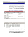
Creating a DC-DC Converter Library Entry
To create a DC-DC converter library entry:
1. To create a DC-DC converter library entry, open the POWR1220AT8
design and click the DC-DC button on the Margin toolbar to open the DCDC Converter Model Selection dialog box. In the dialog box, click New,
enter the name of the DC-DC module (for example, Murata_1V2_POL),
and click Next to open the Select DC-DC Converter Type dialog box.
Figure 57: Adding a DC-DC Converter into the Library
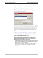
2. The Select the DC-DC Converter Type dialog box (Figure 58) shows four
types of DC-DC converters:
PAC-Designer Software User Manual
54
PAC-Designer Software User Manual
Creating a DC-DC Converter Library Entry
Figure 58: Selecting the DC-DC Converter Type
a. DC-DC Converter with Trim-up & Trim-down Supply – This DC-DC
converter usually is available as a module with a fixed voltage. These
supplies can be margined up and down by connecting a resistor to
GND or to VOUT.
b. DC-DC Converter with Programmable Output Voltage – The output
voltage of these DC-DC converters is set by connecting a resistor
from trim pin to ground. The value of the resistor determines the
output voltage.
c. Programmable DC-DC Converter with Rtrim Connected to Vout – The
output voltage of these DC-DC converters is set by connecting a
resistor from its trim pin to its Vout terminal. The value of the resistor
determines the output voltage.
d. The Discrete implementation represents a class of DC-DC converters
whose output voltage is determined by two resistors: one between the
Vout terminal to the feedback node, and the second between the
feedback node and the ground.
Refer to the DC-DC converter datasheet to select the type of DC-DC
converter and click Next.
PAC-Designer Software User Manual
55
PAC-Designer Software User Manual
Creating a DC-DC Converter Library Entry
3. Configure the DC-DC converter in the subsequent dialog boxes. The
below sub-steps describe how to use the dialog boxes to configure
different types of DC-DC converter.
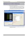
a. Fixed Voltage - DC-DC Converter with Trim-up and Trim-down
Supply
Figure 59 shows the dialog box that appears when DC-DC Converter
with Trim-up & Trim Down Supply is selected in Figure 58. This type
of DC-DC converter is usually a module and is designed to provide a
fixed voltage.
Figure 59: Creating Library Element for a Fixed Voltage DC-DC
Converter
These supplies have a trim pin. This pin is used to margin the supply
up by 5- 10% or margin the supply down by 5-10%.
Nominal Output Voltage is the normal operating voltage of the DC-DC
converter when its trim pin is open. This is its normal operating state.
Next, there are two fields under the headings “Example 1 R to GND,”
“Example 2 R to GND,” and “Example 3 R to Vout.” Examples 1 and 2
are conditions used to generate a margin voltage that is different from
the nominal voltage. Different target voltages will require different
resistor values. These values are provided in the DC-DC converter
PAC-Designer Software User Manual
56
PAC-Designer Software User Manual
Creating a DC-DC Converter Library Entry
datasheet, usually in a table format. Some datasheets provide a
formula to calculate these resistors. Enter the values of the target
output voltage and the values of the target resistors that are
connected between Trim and GND pins into the required fields.
The third column requires the value of the resistor to be connected
between the trim pin and the Vout pin of the DC-DC to achieve the
corresponding output voltage. Enter the resistor value and voltage
values in the required fields. Again, these values can be found in the
DC-DC converter datasheet.
After entering these values, enter the necessary comments that
describe the use of the DC-DC converter and click Finish. In this
case, the software creates a library element called
“Murtata_1V2_POL.”
b. Programmable Voltage with Resistor Connected from Trim Pin to
GND
Figure 60 shows the dialog box that appears when DC-DC Converter
with Programmable Output Voltage is selected in Figure 58.
Figure 60: Setting Reference Voltage/Current for the DC-DC Converter
All DC-DC converters use some type of reference voltage or current to
set the output voltage. The value of the reference voltage “Vref” is
PAC-Designer Software User Manual
57
PAC-Designer Software User Manual
Creating a DC-DC Converter Library Entry
shown either in the specifications section of the datasheet or in its
output voltage calculation formula. Sometimes, the datasheet shows
the architecture of the error amplifier with the value of Vref.
In some cases, the DC-DC converters use current reference instead
of voltage reference. The current reference value is accompanied by a
parallel resistor. Again, some DC-DC converter datasheets show the
equivalent circuit in the error amplifier section. After entering the Vref
or Iref & Rref values, click Next to get the dialog box shown in
Figure 61.
Figure 61: Configuring the Programmable Voltage DC-DC Converter
Library Entry
The output voltage of these types of DC-DC converters is determined
by the resistor connected from their trim pin to GND.
To complete this dialog box, refer to the DC-DC converter datasheet
for a table that maps the resistor values connected between the trim
pin and GND to the desired output voltage values. In some cases, the
DC-DC datasheet provides a formula for calculating the output voltage
for a given trim resistor.
The first field is the output voltage of the DC-DC converter when the
trim pin is open. This is usually one of the entries in the table, or is
PAC-Designer Software User Manual
58
PAC-Designer Software User Manual
Creating a DC-DC Converter Library Entry
calculated using a formula in the datasheet. The two examples
columns are also completed using the same table or the formula in the
datasheet of the DC-DC converter.
Note that one of the voltage values selected should be the maximum
output voltage and the second voltage value should correspond to the
minimum voltage. These voltage values need not be the actual output
voltage used in the circuit board.
Finally, enter the DC-DC converter model name (for example,
Murata_OKYT3_D12) and save the file.
c. Programmable Voltage with Resistor Connected from Trim Pin to
Vout
Figure 62 shows the dialog box that appears when Programmable
DC-DC Converter with Rtrim Connected to Vout is selected in
Figure 58.
Figure 62: Setting Reference Voltage/Current for the DC-DC Converter
All DC-DC converters use some form of reference voltage or current
to set the output voltage. The value of the reference voltage “Vref” is
shown either in the specifications section of the datasheet or in its
output voltage calculation formula. Sometimes the datasheet shows
the architecture of the error amplifier with the value of Vref.
PAC-Designer Software User Manual
59
PAC-Designer Software User Manual
Creating a DC-DC Converter Library Entry
In some cases, the DC-DC converters use current reference instead
of voltage reference. The current reference value is accompanied by a
parallel resistor. Again, some DC-DC converter datasheets show the
equivalent circuit in the error amplifier section. After entering the Vref
or Iref & Rref values, click Next to get the dialog box shown in
Figure 63.
Figure 63: Configuring the Programmable Voltage DC-DC Converter
Library Entry
The output voltage of these types of DC-DC converters is determined
by the resistor connected from their trim pin to GND. To complete this
dialog box, refer to the DC-DC converter datasheet for a table that
maps the output voltage to the resistor values connected between the
trim pin and Vout. In some cases, the DC-DC datasheet provides a
formula for calculating the output voltage for a given trim resistor.
The first field is the output voltage of the DC-DC converter when the
trim pin is open. This is usually one of the entries in the table, or is
calculated using a formula in the datasheet. The two examples
columns are also completed using the same table or the formula in the
datasheet of the DC-DC converter.
Note that one of the voltage values selected should be the maximum
output voltage and the second voltage value should be minimum
PAC-Designer Software User Manual
60
PAC-Designer Software User Manual
Creating a DC-DC Converter Library Entry
voltage. These voltage values need not be the actual output voltage
used in the circuit board.
Finally, enter the DC-DC converter model name (for example,
POL_XYZ) and save the file.
d. Creating a Library Entry for a Discrete DC-DC Converter
These types of DC-DC converters are common when they are realized
using switcher ICs, switching and filter elements. The output voltage is
programmed by connecting two resistors, Rfb and Rin. The output
voltage of the DC-DC converter is calculated using the formula:
Vout = Rfb*Vref / Rin. (Vref is the DC-DC converter reference voltage)
When the DC-DC converter used is of this type, the dialog box shown
in Figure 64 is used to create the library entry.
Figure 64: Creating a Library Entry for a Discrete DC-DC Converter
The dialog box is completed by entering the Rfb and Rin values
calculated for a given output voltage, and Vref, which is found in the
datasheet.
Note that the number of resistors used for controlling these types of
DC-DC converters can be minimized by using the actual voltage that
is used on the board.
PAC-Designer Software User Manual
61
PAC-Designer Software User Manual
Creating a DC-DC Converter Library Entry
4. Once the library entry is created, the next step is to associate the DC-DC
converter from the library to the trim pin. This is done using the following
procedure.
a. Start with the POWR1220AT8 schematic.
b. Double-click the Margin/Trim Block.
c. Double-click the Trim Cell of interest (for example, Trim Cell 1)
d. Set options in the dialog box shown in Figure 65 to design the resistor
network.
Figure 65: Calculating the Resistor Network for a DC-DC Converter
Schematic Net Name – The actual name of the pin in the schematic.
DC-DC Converter – Select the appropriate DC-DC converter from the library
by clicking Import DC-DC. In this example, Murata_OKY3_D12 is selected.
Profile 0 mode – The pull-down menu selects the operating mode of the Trim
Cell: closed loop trim, trim using I2C interface with an external microcontroller,
and EECMOS value (open loop trimming).
Voltage Profile 0 – The nominal operating voltage of the DC-DC converter.
Voltage Profile 1 – One of the margining profiles. It can be the margin-up or
margin-down value.
PAC-Designer Software User Manual
62
PAC-Designer Software User Manual
Creating a DC-DC Converter Library Entry
Voltage Profile 2 – The other margin profile. Again, this can be the margindown or margin-up voltage value.
Voltage Profile 3 – An additional profile provided for convenience. In some
cases, this can be used for additional margin testing.
After entering the required voltage values, click Calculate. The software
calculates the resistors to be placed between the Trim Cell output and the
DC-DC converter trim pin. Calculated DAC code values along with the DAC
currents for each of the profiles are also shown. When you click OK, these
values are stored into the source file.
The Options button opens the following dialog box (Figure 66) for fine tuning
the calculated resistor values.
Figure 66: Optimizing Resistor Values
EIA Resistor Standard – Limits the resistor selection to EIA 12, EIA24,
EIA48, EIA96, EIA192. It also provides a method to calculate the exact
resistor values. The selection of this option depends on design requirements.
Maximum DAC Code Range – Used to provide additional headroom in the
DAC code for maximum voltage variation. This is to account for the errors in
resistor values and the DC-DC converter inaccuracies.
Max Supply Adjustment Range – This is the maximum margin voltage
range with respect to the nominal value that is specified on profile 0. If the
design requires margining of 10%, this value is set to 10%.
Attenuation Crossover Voltage – The maximum input voltage for the ADC is
2.048V. If this ADC is used for measuring voltage higher than the Attenuation
Crossover Voltage, the on-chip 1:3 attenuator should be turned on. This
allows the maximum voltage input to the ADC to increase to 6.144V. This
entry sets the voltage at which the attenuator should be switched on.
Open External Resistor(s) Threshold – The maximum resistor value above
which the resistor is treated as an open circuit. This field can be used to force
the algorithm to minimize the number of resistors to the equivalent circuit. To
do that, first calculate the resistors using the default values. Change the Open
External Resistor(s) Threshold field to a value slightly higher than the series
PAC-Designer Software User Manual
63
PAC-Designer Software User Manual
Creating a DC-DC Converter Library Entry
resistor value and click OK. The software automatically calculates the new
resistors and the associated DAC values.
Vbpz Selection – Usually it is best left as auto. In some cases, by forcing the
Vbpz values to one of the other voltages (0.6V, 0.8V, 1V, or 1.25V), the
number of resistors can be reduced.
After calculating the resistor values for all Trim Cells, the software
automatically saves all the values in to the .PAC file.
To generate a report file of all resistors connected to all Trim Cells, do the
following.
1. Choose File > Export to open the Export dialog box (Figure 67).
Figure 67: Generating a Report File for Margin and Trim
2. Under Export What, select Margin/Trim.
3. Click Browse to select the export file, and click OK.
The output text file format is as shown below:
MarginTrimCell
Idx
0
TrimCellNumber1
TargetVoutSP1
TargetVoutSP2
TargetVoutSP3
TargetVoutSP4
RealizedVoutSP1
RealizedVoutSP2
RealizedVoutSP3
RealizedVoutSP4
VdacCodeSP1
VdacCodeSP2
VdacCodeSP3
PAC-Designer Software User Manual
1.200
1.260
1.140
1.200
1.198
1.256
1.140
1.198
2.000
-6.000
10.000
64
PAC-Designer Software User Manual
Creating a DC-DC Converter Library Entry
VdacCodeSP4
2.000
Vref 0.752
Rbuffer
2561546.920
Rfb
14467007.127
Rin
1000000000.000
Invert
1
IsProgrammable
1
IsModule
1
IsRtGnd
1
Rseries
2400000.000
Rpdn1 10000000.000
Rpup2 10000000.000
Rpdn2 10000000.000
Rpup1 10000000.000
BPZVoltage 0.600
BrickName Murata_OKYT3-D12.xml
BrickFilename
TargetVdacCodesMax
110
EIAStdIdx 1
LooseEIAStdIdx 1
AttenuationCrossoverVoltage 1.900
MaxDeltaVoutPercent
5.000000
RpdnOption 0
Ropen 10000000.000000000000000
BPZSel 0.000000000001056
ResistorComputationAlgorithm 1
MarginTrimCell_end
PAC-Designer Software User Manual
65
PAC-Designer Software User Manual
Creating a DC-DC Converter Library Entry
PAC-Designer Software User Manual
66