1
ispLever
CORE
TM
2.5Gbps Ethernet Media Access Controller IP Core
User’s Guide
August 2007
ipug65_01.0
2.5Gbps Ethernet Media Access Controller
IP Core
Lattice Semiconductor
Introduction
This document provides technical information about the Lattice 2.5Gbps Ethernet Media Access Controller
(2.5Gbps MAC) IP core shown in Figure 1.
The 2.5Gbps MAC IP core comes with the following documentation and files:
• Protected netlist/database
• Behavioral RTL simulation model
• Source files for instantiating and evaluating the core
The 2.5Gbps MAC IP core evaluation package includes a reference design that is used to instantiate, simulate,
map, place and route the core in an example working design. Additional details on this reference design are given
in an appendix of this document.
The 2.5Gbps MAC IP core supports Lattice’s IP hardware evaluation capability, which makes it possible to create
versions of the IP core that operate in hardware for a limited period of time (approximately four hours) without
requiring the purchase of an IP license. It may also be used to evaluate the core in hardware in user-defined
designs. Details for using the hardware evaluation capability are described in the Hardware Evaluation section of
this document.
Features
• Compliant to IEEE 802.3z standard
• Generic 8-bit host interface
• 8-bit wide internal data path
• Generic transmit and receive FIFO interface
• Full-duplex operation
• Transmit and receive statistics vector
• Programmable Inter Packet Gap (IPG)
• Multicast address filtering
• Supports
– Full-duplex control using PAUSE frames
– VLAN tagged frames
– Automatic re-transmission on collision
– Automatic padding of short frames
– Multicast and Broadcast frames
– Optional FCS transmission and reception
– Optional MII management interface module
• Supports jumbo frames up to 9600 bytes
General Description
The 2.5Gbps MAC core can support data rates of 1Gbps or 2.5Gbps in LatticeSC™ and LatticeSCM™ devices.
The 2.5Gbps MAC transmits and receives data between a host processor and an Ethernet network. The main function of the Ethernet MAC is to ensure that the Media Access rules specified in the 802.3 IEEE standards are met
while transmitting and receiving Ethernet frames. Figure 2 shows the frame format of Ethernet packets transmitted
and received on the Ethernet network using the 2.5Gbps MAC.
The data received from the GMII interface is first buffered until sufficient data is available to be processed by the
Receive MAC (Rx MAC). The Preamble and the Start of Frame Delimiter (SFD) information are then extracted from
2
2.5Gbps Ethernet Media Access Controller
IP Core
Lattice Semiconductor
the incoming frame to determine the start of a valid frame. The Receive MAC checks the address of the received
packet and validates whether the frame can be received before transferring it into the FIFO. Only valid frames are
transferred into the FIFO. The 2.5Gbps MAC however always calculates CRC to check whether the frame was
received error-free or not.
When transmitting a frame the DA, SA, L/T, and DATA fields are derived from higher layers. This frame is sent via
the FIFO interface to the Transmit MAC (Tx MAC) where it is encapsulated into an Un-tagged Ethernet frame. This
frame is not sent over the network until the network has been idle for a minimum of Inter Packet Gap (IPG) time.
The Frame encapsulation consists of adding the Preamble bits, the Start of Frame Data (SFD) bits and the CRC
check sum to the end of the frame (FCS). If padding is not disabled, all short frames are padded with hexadecimal
55.
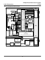
Core Block Diagram
Figure 1. 2.5Gbps Ethernet MAC Core Block Diagram
rxmac_clk
txd
txmac_clk
cpu_if_gbit_en
txen
reset_n
txer
tx_fifodata
GMII
rxd
tx_fifoavail
tx_fifoeof
rxdv
tx_fifoempty
tx_sndpaustim
rxer
tx_sndpausreq
tx_fifoctrl
Receive and
Transmit MAC
tx_staten
tx_macread
hcs_n
haddr
hdatain
tx_statvec
hdataout
tx_done
Host Interface
tx_disfrm
hwrite_n
hread_n
rx_fifo_full
hready_n
rx_write
hdataout_en_n
rx_dbout
hclk
rx_stat_vector
rx_stat_en
ignore_next_pkt
mdc
rx_eof
mdo
rx_error
Management Interface
rx_fifo_error
mdio_en
mdi
Figure 2. Un-Tagged Ethernet Frame Format
PREAMBLE
SFD
DESTINATION
ADDRESS
SOURCE
ADDRESS
LENGTH/
TYPE
DATA/PAD
FRAME CHECK
SEQUENCE
7 bytes
1 byte
6 bytes
6 bytes
2 bytes
46-1500 bytes
4 bytes
A Tagged frame includes a 4-byte VLAN Tag field, which is located between the Source Address field and the
Length/Type field. The VLAN Tag field includes the VLAN Identifier and other control information needed when
operating with Virtual Bridged LANs as described in IEEE P802.1Q.
3
2.5Gbps Ethernet Media Access Controller
IP Core
Lattice Semiconductor
System Block Diagrams
Figure 3 shows a FPGA system level block diagram of how the 2.5Gbps MAC core is instantiated and used in a
1Gbps application with a GMII interface. Note that the MAC core needs a certain amount of support logic like PLLs,
I/O buffers and I/O flip flops to meet the IEEE 802.3 I/O specifications.
Figure 4 shows a FPGA system level block diagram of how the 2.5Gbps MAC core is instantiated and used in a
1Gbps or 2.5Gbps application with a SERDES interface.
Figure 3. 1Gbps System Application Diagram of 2.5Gbps MAC
GMII
ODDR
0
1
gtx_clk_c
125Mhz
rx_clk_c
SYS_CLK
PLL
PLL
txd_pos[7:0]
txen
txer
rxmac_clk
txmac_clk
txdc[7:0]
I/O
FF
I/O
FF
rxdpos[7:0]
cpu_
if _gbit_en
txen
txer
rxdc[7:0]
I/O
FF
GMII
reset_n
tx_fifodata
rxdvpos
rxerpos
tx_fifoavail
I/O
FF
rxdvc
rxerc
tx_fifoeof
tx_fifoempty
tx_sndpaustim
User
Application
Logic
tx_sndpausreq
tx_fifoctrl
tx_staten
Receive and
Transmit MAC
hcs_n
tx_macread
haddr
tx_statvec
hdatain
tx_done
hdataout
tx_disfrm
Host
Interface
rx_fifo_full
rx_write
hwrite_n
hread_n
hready_n
User
Host
Logic
HI
I/O
BUFFs
hdataout_en_n
rx_dbout
hclk
rx_stat_vector
rx_stat_en
ignore_next_pkt
rx_eof
mdc
rx_error
mdio_en
Management
Interface
rx_fifo_error
2.5Gbps MAC IP CORE
FPGA TOP
4
mdo
mdi
SMI
2.5Gbps Ethernet Media Access Controller
IP Core
Lattice Semiconductor
Figure 4. 2.5Gbps System Application Diagram of 2.5Gbps MAC
SYS_CLK
PCS/SERDES
Tx_reference_clock
Tx_Rx_reference_clock_out
hdoutP
txd_pos[7:0]
txd[7:0]
hdoutN
txen
txer
rxmac_clk
txmac_clk
txen
txer
SERIAL
GMII
rxdpos[7:0]
hdinP
rxd[7:0]
cpuifgbiten
GMII
reset_n
hdinN
tx_fifodata
rxdvpos
rxerpos
tx_fifoavail
tx_fifoeof
rxdv
rxer
tx_fifoempty
tx_sndpaustim
tx_sndpausreq
tx_fifoctrl
User
Application
Logic
tx_staten
Receive and
Transmit
MAC
hcs_n
haddr
hdatain
hdataout
tx_macread
tx_statvec
tx_done
tx_disfrm
Host
Interface
rx_fifo_full
rx_write
rx_dbout
hwrite_n
hread_n
hready_n
hdataout_en_n
HI
User
Host
Logic
I/O
BUFFs
hclk
rx_stat_vector
rx_stat_en
ignore_next_pkt
rx_eof
mdc
mdio_en
rx_error
rx_fifo_error
Management
Interface
2.5Gbps MAC IP CORE
FPGA TOP
5
mdo
mdi
SMI
2.5Gbps Ethernet Media Access Controller
IP Core
Lattice Semiconductor
Signal Descriptions
Table 1. 2.5Gbps MAC Input and Output Signals
Port Name
Type
Active
State
Description
Clocks, Reset and Other
rxmac_clk
Input
N/A
Receive MAC Application I/F Clock. This clock is used by the client application and
MAC, all outputs driven by the Rx MAC on the client side are synchronous to this
clock. This clock’s frequency is 125 MHz or 312.5 MHz, depending on the rate of
operation: 1Gbps or 2.5Gbps. All Rx MAC bytes are aligned with this clock. This
clock is derived from the system GMII rx_clk.
txmac_clk
Input
N/A
Transmit MAC Application I/F Clock. This clock is used by the client application
and MAC, all inputs to the Tx MAC on the client side should be synchronous to this
clock. This clock’s frequency is 125 MHz or 312.5 MHz, depending on the rate of
operation: 1 Gbps or 2.5 Gbps. All Tx MAC bytes are aligned with this clock. This
clock is derived from the system sys_clk.
hclk
Input
N/A
Host Clock. This is the Host Bus clock, and is used to clock the Host Bus interface.
mdc
Input
N/A
Management Data Clock. This clock is used only when the Management Interface
module is implemented.
reset_n
Input
Low
Reset. This is an active low signal that resets the internal registers and internal logic.
When activated, the I/O signals are driven to their inactive levels.
hcs_n
Input
Low
Chip Select. This is an active low signal used to select the core for register
read/write operations.
haddr[7:0]
Input
N/A
Address. This selects one of the internal core registers.
hdatain[7:0]
Input
N/A
Data Bus Input. The CPU writes to the internal registers through the data bus.
hwrite_n
Input
Low
Host Write. This active low signal is used to write data to the selected register.
hread_n
Input
Low
Host Read. This active low signal is used to read data from the selected register.
hready_n
Output
Low
Ready. This is an active low signal used to indicate the end of transfer. For write
operations, hready_n is asserted after data is accepted (written). For read operations hready_n is asserted after data on the hdataout bus is ready to be driven out.
hdataout_en_n
Output
Low
Data Out Enable. This signal is driven low whenever the 2.5Gbps MAC outputs valid
data onto the hdataout bus. This signal can be used to build a bi-directional data
bus.
hdataout[7:0]
Output
N/A
Data Bus Output. The CPU reads the internal registers through the data bus.
Host Interface
Transmit MAC Application Interface
tx_fifodata[7:0]
Input
N/A
Transmit FIFO Read Data Bus. The data from the FIFO is presented on this bus.
tx_fifoavail
Input
High
Transmit FIFO Data Available. When asserted, this indicates that the Tx FIFO has
data ready for transmission on the GMII interface. Once this signal is asserted by the
client, a short delay later the frame will be transmitted. Therefore, the client needs to
use an appropriate threshold on the client FIFO to indicate that a frame is ready to be
sent and use that threshold as the tx_fifo_avail signal.
tx_fifoeof
Input
High
Transmit FIFO End of Frame. This signal is asserted along with the last byte of
frame data indicating the end of the frame.
tx_fifoempty
Input
High
Transmit FIFO Empty. This indicates that the Tx FIFO is empty. When this signal is
asserted and the 2.5Gbps MAC is reading the FIFO, the under-run condition is transferred to the network through the txer signal.
tx_sndpaustim[15
:0]
Input
N/A
PAUSE Frame Timer. This indicates the PAUSE time value that should be sent in the
PAUSE frame.
tx_sndpausreq
Input
High
PAUSE Frame Request. When asserted, the 2.5Gbps MAC transmits a PAUSE
frame. This is also the qualifying signal for the tx_sndpausetim bus.
tx_fifoctrl
Input
N/A
FIFO Control Frame. This signal indicates whether the current frame in the Tx FIFO
is a control frame or a data frame. It is qualified by the tx_avail signal. The following
values apply: 1 = Control frame 0 = Normal frame.
6
2.5Gbps Ethernet Media Access Controller
IP Core
Lattice Semiconductor
Table 1. 2.5Gbps MAC Input and Output Signals (Continued)
Port Name
tx_staten
tx_macread
Type
Active
State
Output
High
Transmit Statistics Vector Enable. When asserted, the contents of the statistics
vector bus tx_statvec are valid.
High
Transmit FIFO Read. This is the 2.5Gbps MAC Transmit FIFO read request,
asserted by the 2.5Gbps MAC when it intends to read the client FIFO. The MAC core
will first assert the tx_macread signal if the client FIFO is Not Empty (i.e.,
tx_fifoempty = 0, after which the tx_macread may deassert, based on MAC processing, or re-assert, based on MAC processing and if tx_fifoempty is still 0). The
tx_macread signal should be tied to the client FIFO read pin, and the FIFO empty
pin should be tied to the tx_fifoempty of the MAC core.
Output
Description
tx_statvec[30:0]
Output
N/A
Transmit Statistics Vector. This includes useful information about the frame that
was just transmitted. The corresponding bit locations of this bus are defined as follows:
tx_statvec[0] – UNICAST frame
tx_statvec[1] – Multicast frame
tx_statvec[2] – BROACAST frame
tx_statvec[3] – Bad FCS frame
tx_statvec[4] – JUMBO frame
tx_statvec[5] – FIFO under-run
tx_statvec[6] – PAUSE frame
tx_statvec[7] – VLAN tagged frame
tx_statvec[21:8] – Number of bytes in the transmitted frame
tx_statvec[22] – Deferred transmission
tx_statvec[23] – Excessive deferred transmission tx_statvec[24:26] - RSVD
tx_statvec[30] – FCS generation is disabled and a short frame was transmitted
tx_done
Output
High
Transmit Done. This signal is asserted for one clock cycle after transmitting a frame
if no errors were present in transmission.
tx_discfrm
Output
High
Discard Frame. This signal is asserted at the end of a frame transmit process if the
2.5Gbps MAC detected an error. The possible conditions are: A FIFO under-run The
user application normally moves the pointer to the next frame in these conditions.
Management Interface Signals
mdi
Input
High
Management Data Input. Used to transfer information from the PHY to the management module.
mdo
Output
High
Management Data Output. Used to transmit information from the management
module to the PHY.
mdio_en
Output
High
Management Data Out Enable. Asserted whenever mdo is valid. This may be used
to implement a bi-directional signal for mdi and mdo.
txd_pos[7:0]
Output
High
txd_pos[7:0] - Transmit Data Sent to the PHY. These are the GMII transmit data
signals (txd[7:0]).
txen
Output
High
Transmit Enable. Asserted by the 2.5Gbps MAC to indicate the txd bus contains
valid frame.
txer
Output
High
Transmit Error. Asserted when the 2.5Gbps MAC generates a coding error on the
byte currently being transferred.
rxdv_pos
Input
High
Receive Data Valid. GMII rxdv signal. This signal indicates receive data is valid.
rxd_pos[7:0]
Input
N/A
Receive Data Bus. Data is driven by the PHY on these lines, and is valid whenever
rxdv is asserted.
rxer_pos
Input
High
Receive Data Error. This signal is asserted by the external PHY device when it
detects an error during frame reception.
Input
High
Receive FIFO Full. This signal indicates the Rx FIFO is full and cannot accept any
more data. This is an error condition and should never happen.
Output
High
Receive FIFO Write. This signal is asserted by the 2.5Gbps MAC core to request a
FIFO write.
GMII Signals
Management Interface Signals
rx_fifo_full
rx_write
7
2.5Gbps Ethernet Media Access Controller
IP Core
Lattice Semiconductor
Table 1. 2.5Gbps MAC Input and Output Signals (Continued)
Type
Active
State
rx_dbout[7:0]
Output
N/A
Receive FIFO Data Output. This bus contains the data that is to be written into the
Receive FIFO.
rx_stat_vector[31:0]
Output
N/A
Receive Statistics Vector. This bus indicates the events encountered during frame
reception. This bus is qualified by the rx_stat_en signal. The definition of each signal is explained in the Receive MAC section of this document.
rx_stat_en
Output
High
Receive Statistics Vector Enable. When asserted, this indicates that the contents
of the rx_stat_vector bus is valid.
Input
High
Ignore Next Packet. This signal is asserted by the host to prevent a Receive FIFO
Full condition. The Receive MAC continues dropping packets as long as this signal is
asserted. This is an asynchronous signal.
rx_eof
Output
High
End Of Frame. Indicates all the data for the current packet has passed on to the
FIFO.
rx_error
Output
High
Receive Packet Error. When asserted, this signal indicates the packet contains
error(s). This signal is qualified with the rx_eof signal.
rx_fifo_error
Output
High
Receive FIFO Error. This signal is asserted when the rx_fifo_full signal was
detected asserted during a FIFO write. It is qualified by rx_eof.
Port Name
ignore_next_pkt
Description
Parameter Descriptions
The 2.5Gbps MAC includes one configurable parameter to allow easy integration with the user’s application. The
configurable parameter is shown in Table 2.
Table 2. 2.5Gbps MAC Configuration Parameter
Parameter
Value Range
Default
Description
MIIM_MODULE
Include or Do Not Include
Include
This parameter determines whether the optional MIIM Module will be included in the core’s implementation.
Functional Description
The 2.5Gbps MAC IP core is a fully synchronous machine composed of Transmit and Receive MAC sections that
operate independently to support full duplex operation.
The block diagram of the 2.5Gbps MAC core is shown in Figure 1. The major functional modules are:
• Host interface
• Receive MAC
• Transmit MAC
• Internal buffers and FIFO interfaces
• GMII
• Management Interface Module (Optional)
For 1Gbps operation with the GMII interface, the 125 MHz system clock is supplied to the Transmit MAC. The system clock is used to clock the GMII interface for data transmission. When receiving data, an external PHY device
provides the 125 MHz clock to the GMII receive section. The 125 MHz clock is used to clock the Receive MAC.
For 1Gbps/2.5Gbps operation with SERDES, a PCS/SERDES block in the FPGA is used to tie to the GMII interface of the 2.5Gbps MAC. A reference clock can be sourced to the PCS/SERDES and the reference_out_clk
from the SERDES can be used to clock both the Transmit MAC and the Receive MAC.
8
2.5Gbps Ethernet Media Access Controller
IP Core
Lattice Semiconductor
Host Interface
The Host Interface module is a fully synchronous module that runs off the host clock. A number of registers are initialized via the Host interface to ensure that the 2.5Gbps MAC functions as intended. The write operation to an
internal register is initiated when the hcs_n and hwrite_n signals are asserted and hread_n signal is deasserted. The address of the targeted register is placed on the haddr bus, while the valid data is placed on the
hdatain bus. The contents of the address and data busses should remain unchanged until the 2.5Gbps MAC core
asserts the hready_n signal. The signals cs_n, hwrite_n and hread_n must remain unchanged until
hready_n is asserted.
A register read is initiated by asserting the hcs_n and hread_n signals, while keeping the hwrite_n signal deasserted. The address of the targeted register is placed on the haddr bus. The 2.5Gbps MAC places the content of
the targeted register on the hdataout bus and qualifies it with the assertion of hready_n signal. The haddr bus
should not change until the hready_n signal is asserted.
Figure 11 shows the timing diagram associated with the host interface write and read operations.
Receive MAC (Rx MAC)
The main function of the Rx MAC is to accept the formatted data from the GMII interface and pass it to the host
through an external FIFO. In this process, the Rx MAC performs the following functions:
• Detect the Start of Frame
• Compare the MAC address
• Re-calculate CRC
• Process the Control Frame and pass it to the flow control module.
The Rx MAC operation is determined by programming the MODE and TX_RX_CTL registers. Programming the
MODE and TX_RX_CTL registers can control the Receive MAC operation. The various events that occur during the
reception of a frame are logged into the rx_stat_vector signal and the TX_RX_STS register. At the end of
reception, the rx_stat_en signal is asserted to qualify the rx_stat_vector signal. The 2.5Gbps MAC core can
report a wealth of information such as
• FIFO overflow
• CRC error
• Receive error
• Short frame reception
• Long frame reception
• IPG violation
By default, the entire frame, except the preamble and SFD bytes, is sent to the FIFO via the Rx MAC application
interface signals. If the user does not want to receive the FCS, the core can be programmed to strip the FCS field
as well as any PAD bytes in the frame and send the rest to the FIFO.
The Rx MAC section operates on the rxmac_clk derived from the clock sourced from the PHY. All the signals on
the Receive MAC FIFO interface are synchronous to this clock.
The Rx MAC is disabled while reset_n is low and should only be enabled after the associated registers are properly initialized.
9
2.5Gbps Ethernet Media Access Controller
IP Core
Lattice Semiconductor
Receiving Frames
The frames received by the Rx MAC are analyzed and the Preamble and SFD bytes are stripped off the frame
before it is transferred to an external FIFO. The interface between the MAC and the FIFO is 8 bits wide.
The default behavior of the MAC is to transfer the unmodified frame after stripping off the Preamble and SFD bytes.
This behavior can be changed by setting bit [1] of the TX_RX_CTL register. When bit [1] is set, the Rx MAC strips
the Preamble, SFD, FCS bytes and the PAD bytes, if any.
Once the frame is ready to be written into the FIFO, the Rx MAC asserts the rx_write signal, then presents the
data on the rx_dbout bus. The rx_write signal is asserted as long as the frame is being written. After transferring the entire frame into the FIFO, the Rx MAC asserts rx_eof, indicating the end of the frame. If the frame is
received with errors, rx_error is asserted along with rx_eof. If the frame is received with no errors, rx_error
remains de-asserted. In either case, a rich set of statistics vectors is presented, containing information about the
frame that was received. The statistics vector bus, rx_stat, is qualified by the assertion of rx_stat_en.
If the RxFIFO becomes full, rx_fifo_full is asserted and the frame data is lost. Therefore, the FIFO full condition must be avoided at all times. The rx_fifo_error signal will be asserted along with rx_eof for all frames
written into the FIFO while it is full.
The Rx MAC goes to the IDLE state when it is done receiving the frame. This is indicated by bit[10] of the
TX_RX_STS register. If the Rx MAC is disabled while it is in the process of receiving a frame, it goes to the IDLE
state after it completes the current frame reception.
Address Filtering
The Rx MAC offers several address filtering methods to effectively block unwanted frames. It also provides a PROMISCUOUS mode, in which all supported filtering schemes are abandoned and the Receive MAC transfers all the
frames irrespective of the address they contain.
By default, the Rx MAC is configured to filter and discard Broadcast and Multicast frames. The MAC can be configured to receive Broadcast frames by setting bit [7] of the TX_RX_CTL register. Multicast frames are received only
when bit [4] of the TX_RX_CTL register is set. When set, the Multicast frames are subject to filtering that is dependent on a hash table lookup. The six middle bits of the most significant byte of the CRC, calculated for the destination address field of the frame, are used to address one of the 64 bits of the hash table. If the retrieved bit is set, a
Multicast addressed frame is received. If not, it is discarded.
All other regular frames are filtered based on the Rx MAC address programmed into the MAC_ADDR_0,
MAC_ADDR_1 and MAC_ADDR_2 registers.
Filtering based on Frame Length
The default minimum Ethernet frame size is 64 bytes. Any frame smaller than 64 bytes could possibly be a collision
fragment. By default, the Rx MAC is configured to ignore bytes shorter than 64 bytes. The user can configure the
MAC to receive shorter frames by setting bit [8] of the TX_RX_CTL register. Whenever a short frame is received,
the appropriate bit is set in the statistics vector, marking it as a Short frame.
The Rx MAC has been designed to receive frames larger than the standard specified maximum as easily as any
other frame. This ensures the MAC can work in environments that can generate jumbo frames. However, for statistics purposes, the user can set the maximum length of the frame in the MAX_PKT_SIZE register. When a received
frame is larger than the number in this register, bit [31] of the Receive Statistics Vector bus is set, marking it as a
Long frame.
Receiving a PAUSE Frame
When the Rx MAC receives a PAUSE frame, the Tx MAC continues with the current transmission, then pauses for
the duration indicated in the PAUSE time. During this time, the Tx MAC can transmit Control frames.
Although PAUSE frames may contain the Multicast Address, Multicast filtering rules do not apply to them. If bit [3]
of the TX_RX_CTL register is set, the Rx MAC will signal the Tx MAC to stop transmitting for the duration specified
10
2.5Gbps Ethernet Media Access Controller
IP Core
Lattice Semiconductor
in the frame. If this bit is reset, the Rx MAC assumes the Tx MAC does not have the PAUSE capability and/or does
not wish to be paused and will not signal it to stop transmitting. In either case, the PAUSE frame is received and
transferred to the FIFO.
Statistics Vector
By default, a Statistics Vector is generated for all received frames transferred to the external FIFO. If the user wants
the Rx MAC to ignore all incoming frames, then the input signal ignore_next_pkt must be asserted. In this
case, a frame that should have been received is ignored and the Rx MAC sets the Packet Ignored bit (bit 26) of the
Statistics Vector.
The MAX_PKT_SIZE register is programmed by the user as a threshold for setting the Long Frame bit of the Statistics Vector. This value is used for Un-tagged frames only. The Receive MAC will add “4” to the value specified in this
register for all VLAN tagged frames when checking against the number of bytes received in the frame. This is
because all VLAN tagged frames have additional four bytes of data.
When a tagged frame is received, the entire VLAN tag field is stored in the VLAN_TAG register. Additionally, every
time a statistics vector is generated, some of the bits are written into the corresponding bit locations [9:1] of the
TX_RX_STS register. This is done so the user can get this information via the Host interface.
The description of the bits in the Statistics Vector bus is shown in Table 3.
Table 3. Receive Statistics Vector Description
Bit
Description
31
Long Frame. This bit is set when a frame longer than that specified in the MAX_PKT_SIZE register is received.
30
Short Frame. This bit is set when a frame shorter than 64 bytes is received.
29
IPG Violation. This bit is set when a frame is received before the IPG timer runs out.
28
Preamble Shrink. This bit is asserted if the number of Preamble bytes received is not equal to seven.
27
Carrier Event Previously Seen. This bit is set when the SFD field was not found in a received packet but the
data valid was asserted.
26
Packet Ignored. When set, this indicates the incoming packet is to be ignored.
25
CRC Error. This bit is set when a frame is received with an error in the CRC field.
24
Length Check OK. This bit is set if the number of data bytes in the incoming frame matches the value in the
length field of the frame.
23
Receive OK. This bit is set if the frame is received without any error.
22
Multicast Address. This bit is set to indicate the received frame contains a Multicast Address.
21
Broadcast Address. This bit is set to indicate the received frame contains a Broadcast Address.
20
Not used.
19
Unsupported Opcode. This bit is set if the received control frame has an unsupported opcode. In this version
of the IP, only the opcode for a PAUSE frame is supported.
18
Control Frame. This bit is set to indicate that a Control frame was received.
17
PAUSE Frame. This bit is set when the received Control frame contains a valid PAUSE opcode.
16
VLAN Tag Detected. This bit is set when the 2.5Gbps MAC receives a VLAN Tagged frame.
15:0
Frame Byte Count. This contains the length of the frame that was received. The frame length includes the DA,
SA, L/T, TAG, DATA, PAD and FCS fields.
Transmit MAC (Tx MAC)
The Tx MAC is responsible for controlling access to the physical medium. The TxMAC reads data from an external
TxFIFO when it detects an active tx_fifoavail. The Tx MAC then formats this data into an Ethernet packet and
passes it to the GMII module.
The Tx MAC is disabled while reset_n is low and should only be enabled only after the associated registers are
properly initialized. Once enabled, the Tx MAC will continuously monitor the FIFO interface for an indication that
11
2.5Gbps Ethernet Media Access Controller
IP Core
Lattice Semiconductor
frame(s) are ready to be transmitted. The Tx MAC and the TxFIFO interface operations are synchronous to
txmac_clk.
It is possible for the receiver’s buffer to fill up rapidly. In such cases, the receiver sends flow control (PAUSE) frames
to the transmitter, requesting that it stop transmitting frames. When the receiver is able to free the buffers, the transmitter completes transmitting the current frame and stops for the duration specified in the PAUSE frame.
Transmitting Frames
By default, the Transmit MAC is configured to generate the FCS pattern for the frame to be transmitted. However,
this can be prevented by setting bit[2] of the Tx_RX_CTL register. This feature is useful if the frames being presented for transmission already contain the FCS field. When FCS field generation by the MAC is disabled, it is the
user’s responsibility to ensure that short frames are properly padded before the FCS is generated. If the MAC
receives a frame shorter than 64 bytes when FCS generation is disabled, the frame is sent as is and a statistic vector for the condition is generated.
The DA, SA, L/T, and DATA fields are derived from higher applications through the FIFO interface and then encapsulated into an Un-tagged Ethernet frame. This frame is not sent over the network until the network has been idle
for a minimum of Inter Packet Gap (IPG) time. The Frame encapsulation consists of adding the Preamble bits, the
Start of Frame Data (SFD) bits and the CRC check sum to the end of the frame (FCS). If padding is not disabled,
all short frames are padded with hexadecimal 55.
The input signal tx_eof is asserted along with the last set of data transfer to indicate the end of the frame. The Tx
MAC requires a continuous stream of data for the entire frame. There cannot be any bubbles of “no data transfer”
within a frame. If the MAC is able to transmit the frame without any errors, the tx_done signal is asserted. Once
the transmission has ended, data on the tx_stat_vector bus is presented to the host, including all the statistical
information collected in the process of transmitting the frame. Data on this bus is qualified by assertion of the
tx_staten signal.
After the Transmit MAC is done transmitting a frame, it waits for more frames from the FIFO interface. During this
time, it goes to an idle state that can be detected by reading the TX_RX_STS register. Since the MODE register can
be written at any time, the Tx MAC can be disabled while it is actively transmitting a frame. In such cases, the MAC
will completely transmit the current frame and then return to the IDLE state. The control registers should be programmed only after the MAC has returned to the IDLE state.
External Transmit FIFO
The interface between the Tx MAC and the FIFO is 8 bits wide. The bit presented on position 0 is transmitted first
and the bit in position 7 is transmitted last. In other words, bit[0] will be transmitted on the txd[0] signal of GMII while
the bit[7] will be transmitted on txd[7].
The FIFO signals the MAC if the frame ready for transmission at the head of the FIFO is a Control frame. This is
done so the Tx MAC can continue transmission of a Control frame while it is paused.
FIFO Under-flow
If a FIFO underflow occurs, the FIFO logic must assert tx_fifoempty. If at least 64 bytes have been transmitted,
the Tx MAC aborts the transmission by asserting tx_er. In addition, the Tx MAC inserts erroneous CRC bits into
the packet to guarantee the receiver will detect the error in the packet. If less than 64 bytes have been transmitted
when the FIFO underflow occurs, the MAC will pad the remaining bytes before ending the transmission. In either
case, the MAC asserts tx_disframe indicating an error during transmission.
Transmitting PAUSE Frame
Two different methods are used for transmitting a PAUSE frame. In the first method, the application layer forms a
PAUSE frame and submits it for transmission via the FIFO. In the other method, the application layer signals the Tx
MAC directly to transmit a PAUSE frame. This is accomplished by asserting tx_sndpausreg. In this case the Tx
MAC will complete transmission of the current packet and then transmit a PAUSE frame with the PAUSE time value
supplied through the tx_sndpaustim bus.
12
2.5Gbps Ethernet Media Access Controller
IP Core
Lattice Semiconductor
Internal Data Buffer and FIFO Interfaces
The core provides a feature where the user can block all the frames that are shorter than the minimum frame length
of 64 bytes in the 2.5Gbps MAC itself. This prevents any short frames from reaching the user’s application. The
Receive Section contains an internal buffer to support this feature.
External Transmit and Receive FIFOs are required to store variable-length normal packets
The 2.5Gbps MAC provides two independent interfaces for use with external Transmit and Receive FIFOs. This
feature enables the 2.5Gbps MAC to support full duplex operation.
GMII Interface
The GMII module uses the clock supplied by the external PHY. The core implements the standard GMII interface to
connect to the PCS layer.
The module implementing the interface also converts the data to a format usable by the MAC. The 8-bit data at the
interface is presented to the 8-bit data path of the MAC.
Although not implemented as a separate module, the Reconciliation Sub-layer is implemented as a part of the GMII
interface. This module is responsible for passing the data from one clock domain (2.5Gbps MAC) to the other GMII.
(Optional) Media Independent Interface Management Module (MIIM)
The MIIM accesses management information from the PHY device and writes to or reads from the PHY registers.
A single MIIM can address up to 32 PHY devices. This module runs off its own clock called mdc. The standard
specifies this clock to be at 2.5 MHz, but PHY devices can accept a 10-MHz mdc clock. Therefore, the 2.5Gbps
MAC can have a MIIM that is capable of running at up to 10 MHz.
The MIIM read or write operations are specified in the GMII_MNG_CTL register. This register also specifies the
addressed PHY and the register within the PHY that needs to be accessed. The Command Finished bit in the
GMII_MNG_CTL register is reset as soon as a command to read or write is given. It is set only when the MIIM module completes the operation. While the interface is busy, the GMII_MNG_CTL register cannot be overwritten, and all
write operations to the register are ignored. For a write operation, the data to be written is stored in the
GMII_MNG_DAT register. For a read operation, the data read from the addressed PHY is stored in this register. The
ready bit in the GMII_MNG_CTL is set at the end of the read/write operation.
Internal Registers
The 2.5Gbps MAC internal registers are initialized through the generic Host Interface. These rules apply when
accessing the internal registers:
• With the 8-bit Host Interface, the individual bytes of the registers are accessed through their corresponding
addresses, with the lower address pointing to the lower byte.
• The reserved bits should be programmed to 0. These bits are invalid, and should be discarded when read.
• All registers except the MODE register can be written into only when the core is in the IDLE state. The MODE
register is the only register that can be written after the 2.5Gbps MAC is no longer in the Reset condition.
Table 4 lists the 2.5Gbps MAC registers accessible via the Host Interface. The registers are either Read/Write
(R/W) or Read Only (RO) for status reporting purposes. The values of the registers immediately after the Reset
Condition is removed from the 2.5Gbps MAC (POR Value in Hexadecimal format) are also given.
Table 4. 2.5Gbps MAC Internal Registers
Register Description
Mode register
Transmit and Receive Control register
Mnemonic
I/O Address
POR Value
MODE
00H - 01H
0000H
TX_RX_CTL
02H - 03H
0000H
13
2.5Gbps Ethernet Media Access Controller
IP Core
Lattice Semiconductor
Register Description
Maximum Packet Size register
Mnemonic
I/O Address
MAX_PKT_SIZE
04H - 05H
0001H
IPG_VAL
08H - 09H
000CH
Inter Packet Gap register
POR Value
2.5Gbps MAC Address register 0
MAC_ADDR_0
0AH - 0BH
0000H
2.5Gbps MAC Address register 1
MAC_ADDR_1
0CH - 0DH
0000H
2.5Gbps MAC Address register 2
MAC_ADDR_2
0EH - 0FH
0000H
Transmit and Receive Status
TX_RX_STS
12H - 13H
0000H
GMII Management Interface Control register
GMII_MNG_CTL
14H - 15H
0000H
GMII Management Data register
GMII_MNG_DAT
16H - 17H
0000H
VLAN Tag Length/type register
VLAN_TAG
32H - 33H
0000H
Multicast_table_0
MLT_TAB_0
22H - 23H
0000H
Multicast_table_1
MLT_TAB_1
24H - 25H
0000H
Multicast_table_2
MLT_TAB_2
26H - 27H
0000H
Multicast_table_3
MLT_TAB_3
28H - 29H
0000H
Multicast_table_4
MLT_TAB_4
2AH - 2BH
0000H
Multicast_table_5
MLT_TAB_5
2CH - 2DH
0000H
Multicast_table_6
MLT_TAB_6
2EH - 2FH
0000H
Multicast_table_7
MLT_TAB_7
30H - 31H
0000H
PAUS_OP
34H - 35H
0080H
Pause_opcode
Register Descriptions
MODE (R/W)
Mnemonic: MODE
POR Value = 0001H
Name
Range
Description
Rsvd
15:4
Tx_en
3
Transmit Enable. When this bit is set, the Tx MAC is enabled to transmit frames.
When reset, the Tx MAC completes transmission of the packet currently being
processed, then stops.
Rx_en
2
Receive Enable. When this bit is set, the Rx MAC is enabled to receive frames.
When reset, the Rx MAC completes reception of the packet currently being processed, then stops.
FC_en
1
Flow-control Enable. When set, this enables the flow control functionality of the
Tx MAC. This bit should be set for the Tx MAC either to pause or to transmit a
PAUSE frame.
Rsvd
0
Reserved (always reads back as a high).
Reserved.
14
2.5Gbps Ethernet Media Access Controller
IP Core
Lattice Semiconductor
Transmit and Receive Control (R/W)
Mnemonic: TX_RX_CTL
POR Value = 0000H
This register can be overwritten only when the Rx MAC and the Tx MAC are disabled. This register controls the various features of the MAC.
Name
Rsvd
Range
15:9
Description
Reserved.
Receive_short
8
Receive Short Frames. When high, enables the Rx MAC to receive frames
shorter than 64 bytes.
Receive_brdcst
7
Receive Broadcast. When high, enables the Rx MAC to receive broadcast
frames
Rsvd
6
Reserved.
Rsvd
5
Reserved.
Receive_mltcst
4
Receive Multicast. When high, the multicast frames will be received per the filtering rules for such frames. When low, no Multicast (except PAUSE) frames will
be received.
Receive_pause
3
Receive PAUSE. When set, the Rx MAC will indicate the PAUSE frame reception
to the Tx MAC. In either case, PAUSE frames are received and transferred to the
FIFO.
Tx_dis_fcs
2
Transmit Disable FCS. When set, the FCS field generation is disabled in the Tx
MAC.
Discard_fcs
1
Rx Discard FCS and Pad. When set, the FCS and any of the padding bytes are
stripped off the frame before it is transferred to the FIFO. When low, the entire
frame is transferred as is.
Prms
0
Promiscuous Mode. When asserted, all filtering schemes are abandoned and
the Rx MAC receives frames with any address.
Maximum Packet Size (R/W)
Mnemonic: MAX_PKT_SIZE
POR Value = 05EEH (1518 decimal)
This register can be overwritten only when the MAC is disabled. All frames longer than the value (number of bytes)
in this register will be tagged as long frames.
Name
Max_frame
Range
15:0
Description
Maximum size of the packet than can be handled by the core.
IPG (Inter Packet Gap) (R/W)
Mnemonic: IPG_VAL
POR Value = 000CH
This register contains the IPG value to be used by the TX MAC only. Back-to-back packets in the transmit buffer will
be sent out with the IPG setting programmed in this register. Note that the IPG for received packets is checked
against a fixed value of 96 bit times.
Name
Range
Description
Rsvd
15:5
Reserved.
IPG
4:0
Inter-packet gap value in units of byte time.
15
2.5Gbps Ethernet Media Access Controller
IP Core
Lattice Semiconductor
MAC Address Register {0,1,2} (R/W), Set of Three
Mnemonic: MAC_ADD
POR Value = 0000H
The MAC Address Registers 0-2 contain the Ethernet address of the port. The MAC Address Register [0] has the
two bytes that are transmitted first and the MAC Address Register [2] has the two bytes that are transmitted last.
Bit[8] through Bit[15] are transmitted first while bit[0] through bit[7] are transmitted last.
Note that the MAC address is stored in the registers in Hexadecimal form. For example, to set the MAC Address to:
AC-DE-48-00-00-80 would require writing 0xAC (octet 0) to address 0x0B (high byte of Mac_addr[15:0]), 0xDE
(octet 1) to address 0x0A (Low byte of Mac_addr[15:0]), 0x48 (octet 2) to address 0x0D (high byte of
Mac_addr[15:0]), 0x00 (octet 3) to address 0x0C (Low byte of Mac_addr[15:0]), 0x00 (octet 4) to address 0x0F
(high byte of Mac_addr[15:0]), and 0x80 (octet 5) to address 0x0E (Low byte of Mac_addr[15:0]). Note that octet 0
is transmitted first and octet 5 is transmitted last.
Name
Mac_addr
Range
15:0
Description
Ethernet address assigned to the port supported by the 2.5Gbps MAC.
Transmit and Receive Status (RO)
Mnemonic: TX_RX_STS
POR Value = 0000H
This register reports events that have occurred during packet reception and transmission.
Name
Rsvd
Range
15:11
Description
Reserved.
Rx_idle
10
Receive MAC Idle. Receive MAC in idle condition used to reset configurations
by CPU interface.
Tagged_frame
9
Tagged Frame. Tagged frame received.
Brdcst_frame
8
Broadcast Frame. Indicates that a Broadcast packet was received.
Multcst_frame
7
Multicast Frame. Indicates that a Multicast packet was received.
IPG_shrink
6
IPG Shrink. Received frame with shrunk IPG (IPG < 96 bit time).
Short_frame
5
Short Packet. Indicates that a packet shorter than 64 bytes has been received.
Long_frame
4
Too Long Packet. Indicates receipt of a packet longer than the maximum allowable packet size specified in the MAX_PKT_SIZE register.
Error frame
3
Rx_er Asserted. Indicates the frame was received with the rx_er signal
asserted.
CRC
2
CRC Error. Indicates a packet was received with a CRC error.
Pause_frame
1
PAUSE Frame. Indicates a PAUSE frame was received.
Tx_idle
0
Transmit MAC Idle. Transmit MAC in idle condition, used to reset configurations
by CPU interface.
VLAN Tag (RO)
Mnemonic: VLAN_TAG
POR Value = 0000H.
The VLAN tag register has the VLAN TAG field of the most recent tagged frame that was received. This is a read
only register.
Name
VLAN
Range
Description
15:0
This field defines length/type of field of the VLAN tag when inserted into transmitted frames.
16
2.5Gbps Ethernet Media Access Controller
IP Core
Lattice Semiconductor
GMII Management Register Access Control (R/W)
Mnemonic: GMII_MNG_CTL
POR Value = 0000H
The GMII Management Access register controls the Management Interface Module. This register can be overwritten only when the interface is not busy. A write operation will be ignored when the interface is busy.
Name
Range
Description
Rsvd
15
Reserved.
Cmd_fin
14
Command Finished. When high, it means the interface has completed the
intended operation. This bit is set to 0 when the interface is busy.
RW_phyreg
13
Read/Write PHY Registers. 1 = write operation, 0 = read operation
Phy_add
12:8
GMII PHY Address. The address of the accessed PHY Bit 12 is the most significant bit, and it is the first PHY address bit to be transmitted and received.
Rsvd
7:5
Reserved.
Reg_add
4:0
GMII Register Address. The address of the register accessed. Bit 4 is the most
significant bit and is the first register address bit to be transmitted or received.
GMII Management Access Data (R/W)
Mnemonic: GMII_MNG_DAT
POR Value = 0000H.
The contents of this register will be transmitted when a write operation is to be performed. When a read operation
is performed, this register will contain the value that was read from a PHY register. This register should be read
only after the cmd_fin bit in the control register is set.
Name
GMII_dat
Range
Description
GMII Data. Bit 15 is the most significant bit, corresponding to bit 15 of the
accessed register.
15:0
Multicast Tables (R/W), set of eight
Mnemonic: MLT_TAB_[0-7]
POR Value = 0000H.
When the core is programmed to receive multicast frames, a filtering scheme is used to decide whether the frame
should be received. The six middle bits of the most significant byte of the CRC value, calculated for the destination
address, are used as a key to the 64-bit hash table. The three most significant bits select one of the eight tables,
and the three least significant bits select a bit. The frame is received only if this bit is set.
Name
Range
Multicast_table_[0-7]
15:0
Description
Multicast Table. Eight tables that make a 64-bit hash.
Pause Opcode (R/W)
Mnemonic: PAUS_OP
POR Value = 0080H
This register contains the PAUSE Opcode, This will be compared against the Opcode in the received PAUSE
frame. This value will also be included in any PAUSE frame transmitted by the 2.5Gbps MAC. Bit 15 is transmitted
first and bit 0 is transmitted last.
Name
Pause_OpCode
Range
15:0
Description
PAUSE Opcode.
17
2.5Gbps Ethernet Media Access Controller
IP Core
Lattice Semiconductor
Timing Diagrams
The operational timing diagrams applicable to the 2.5Gbps MAC interfaces are shown below:
Reception of a 64-Byte Frame without Error – Rx MAC Application Interface
Figure 5. Reception of a 64-byte Frame without Error
rxmac_clk
rx_dbout[7:0]
1
2
3
62
63
64
rx_write
rx_stat_en
Valid
rx_stat_vector[31:0]
rx_eof
rx_error
rx_fifo_error
Reception of a 64-byte Frame with Error(s) – Rx MAC Application Interface
The signal rx_error is asserted to indicate that the 64-byte frame was received with error(s).
Figure 6. Reception of a 64-byte Frame with Error
rxmac_clk
rx_dbout[7:0]
1
2
3
62
63
64
rx_write
rx_stat_en
Valid
rx_stat_vector[31:0]
rx_eof
rx_error
rx_fifo_error
18
2.5Gbps Ethernet Media Access Controller
IP Core
Lattice Semiconductor
Reception of a 64-Byte Frame with FIFO Overflow – Rx MAC Application Interface
The FIFO writing operation is suspended whenever an overflow condition occurs. When this condition occurs, the
2.5Gbps MAC asserts rx_fifo_error. This signal should be sampled along with rx_eof in order to process the
error condition.
Figure 7. Reception of a 64-byte Frame with FIFO Overflow
rxmac_clk
rx_dbout[7:0]
1
2
3
62
63
64
rx_write
rx_stat_en
rx_stat_vector[31:0]
Valid
rx_eof
rx_error
rx_fifo_full
rx_fifo_error
Successful Transmission of a 64-Byte Frame – Tx MAC Application Interface
The assertion of tx_fifoavail indicates a frame is ready to be transmitted. The 2.5Gbps MAC reads the FIFO
and the data is transmitted until tx_fifoeof is asserted. Once the frame is transmitted, tx_staten is asserted
to qualify the statistic vector, tx_statvec. The signal tx_done is asserted to indicate a successful transmission.
This is shown in Figure 8.
Figure 8. Transmission of a 64-Byte Frame without Error
txmac_clk
tx_fifoavail
tx_fifodata[7:0]
1
2
62
63
64
tx_macread
tx_staten
tx_staten[31:0]
Valid
tx_fifoeof
tx_fifoempty
tx_discfrm
tx_done
19
2.5Gbps Ethernet Media Access Controller
IP Core
Lattice Semiconductor
Successful Transmission of a 64-byte Frame with FIFO Empty – Tx MAC Application
Interface
tx_fifoempty is asserted along with tx_fifoe to indicate that the complete 64-byte frame has been read. The
frame is transmitted as a valid frame and tx_done is asserted at the end of transmission.
Figure 9. Successful Transmission of a 64-byte Frame with FIFO Empty
txmac_clk
tx_fifoavail
tx_fifodata[7:0]
1
62
2
63
64
tx_macread
tx_staten
tx_staten[31:0]
Valid
tx_fifoeof
tx_fifoempty
tx_discfrm
tx_done
Aborted Transmission Due to FIFO Empty – Tx MAC Application Interface
If the tx_fifoempty is asserted while the Tx MAC is in the process of reading a frame, the MAC will stop reading
the frame and assert tx_disfrm to indicate an erroneous transmission. The frame transmission is abandoned
when this occurs.
Figure 10. Aborted Transmission Due to FIFO Empty
txmac_clk
tx_fifoavail
tx_fifodata[7:0]
1
62
2
63
64
tx_macread
tx_staten
tx_staten[31:0]
Valid
tx_fifoeof
tx_fifoempty
tx_discfrm
tx_done
20
2.5Gbps Ethernet Media Access Controller
IP Core
Lattice Semiconductor
Host Interface Read/Write Operation
During a write operation, haddr associated with hdatain, hcs_n and hwrite_n performs a write operation to an
internal register. The end of transaction is indicated by assertion of hready_n. During a read operation, haddr
associated with hcs_n and hread_n forms a write operation. The end of transaction is indicated by the assertion
of hready_n and hdataout_en_n along with the valid read data on hdataout.
Figure 11. Host Interface Read/Write Operation
hclk
haddr
[addr_width-1:0]
ADDR
hdatain
[data_width-1:0]
DATA
A
ADDR
B
A
hdataout
[data_width-1:0]
DATA B
hcs_n
hread_n
hwrite_n
hready_n
hdataout_en_n
READ OPERATION
WRITE OPERATION
Management Interface Read/Write Operation
During a write operation, mdio_en is asserted and the data is transmitted on mdo. During a read operation,
mdio_en is asserted while the address is being transferred. Once this is done, it is de-asserted for rest of the
transfer enabling the PHY to deliver data on mdi.
Figure 12. Management Interface Read and Write Operations
mdc
mdio_en
mdo
address and write data
address of register being read
mdi
read data
WRITE
OPERATION
READ
OPERATION
GMII Transmit and Receive Operations
txd and tx_en are driven synchronous to the gtx_clk during transmit operations. When the frame being transmitted has an error, tx_er is asserted. Note that in 2.5Gbps operation with a SERDES interface, the gtx_clk is
the transmit reference clock (see Figure 4).
When receiving data, rxd and rx_en are sampled on the rising edge of rx_clk. An error in the frame is indicated
when rx_er is asserted. Note that in 2.5Gbps operation with a SERDES interface, the rx_clk is the
Tx_Rx_reference_clock (see Figure 4).
21
2.5Gbps Ethernet Media Access Controller
IP Core
Lattice Semiconductor
Figure 13. GMII Transmit and Receive Operations
gtx_clk
tx_en
txd[0:7]
VALID FRAME DATA
VALID FRAME DATA
tx_er
FRAME WITH
ERROR
FRAME WITHOUT
ERROR
rx_clk
rx_en
rxd[0:7]
VALID FRAME DATA
VALID FRAME DATA
rx_er
FRAME WITH
ERROR
FRAME WITHOUT
ERROR
Core Generation
The 2.5Gbps MAC IP core is available for download from the Lattice website at www.latticesemi.com. The IP files
are automatically installed using ispUPDATE technology in any user-specified directory.
The ispLEVER® IPexpress™ GUI window for the 2.5Gbps MAC core is shown in Figure 14. To generate a specific
IP core configuration the user specifies:
• Project Path – Path to directory where the generated IP files will be loaded.
• File Name – “username” designation given to the generated IP core and corresponding folders and files.
• Design Entry Type – Verilog.
• Device Family – Device family to which IP is to be targeted (e.g. LatticeXP™, LatticeEC™, LatticeECP™, etc.).
Only families that support the particular core are listed.
• Part Name – Specific targeted device within the selected device family.
Note that if IPexpress is called from within an existing project, Project Path, Design Entry, Device Family and Part
Name default to the specified project parameters.
22
2.5Gbps Ethernet Media Access Controller
IP Core
Lattice Semiconductor
Figure 14. 2.5Gbps MAC IPexpress GUI Window
To create a custom configuration, the user then clicks on the Customize button to display the 2.5Gbps MAC IP
core Configuration GUI, shown in Figure 15. From this window the user may select to instantiate the optional MII
Management Interface Module.
Evaluation configuration options are also provided which allow users to specify a synthesis tool (Synplify® or Precision® RTL Synthesis) to synthesize the top-level level configurations and the desired data rate to be supported by
the evaluation configurations. Note that these configuration options only affect the ispLEVER properties and preferences applied in implementing the evaluation top-level designs.
23
2.5Gbps Ethernet Media Access Controller
IP Core
Lattice Semiconductor
Figure 15. 2.5Gbps MAC IPexpress GUI Window
After the Generate button has been clicked, the configuration-specific IP core and supporting files are generated in
the user’s project directory. The directory structure of the generated files is shown in Figure 16.
Figure 16. 2.5Gbps MAC IP Core Generated Directory Structure
24
2.5Gbps Ethernet Media Access Controller
IP Core
Lattice Semiconductor
The following files are generated in the user’s project directory (\2g5mac_test in Figure 16):
• <username>.lpc – IP parameter file (may be directly modified by user).
• <username>.ngo – Synthesized and mapped IP core.
• <username>_bb.v – Black box module wrapper for synthesis.
• <username>_inst.v – Example of instantiation template to be included in user’s design.
• <username>_beh.v – Behavioral simulation model for IP core configuration username.
These are all of the files needed to implement and verify the 2.5Gbps MAC IP core in a top-level design. The following additional files providing IP core generation status information and command line generation capability are generated in the user’s project directory:
• <username>_generate.tcl – Created when GUI Generate button is clicked, invokes generation, may be run from
command line.
• <username>_generate.log – ispLEVER synthesis and map log file.
• <username>_gen.log – IPexpress IP generation log file.
The \<2g5mac_eval> and subtending directories provide files supporting 2.5Gbps MAC core evaluation. The
\<2g5mac_eval> directory shown in Figure 16 contains files and folders with content that is constant for all configurations of the 2.5Gbps MAC. The \<username> subfolder (\mac_core0 in this example) contains files/folders
with content specific to the username configuration.
The \2g5mac_eval directory is created by IPexpress the first time the core is generated and updated each time
the core is regenerated. A \<username> directory is created by IPexpress each time the core is generated and
regenerated each time the core with the same file name is regenerated. A separate \<username> directory is
generated for cores with different names (e.g. \<mac0>, \<mac1>, etc.).
Instantiating the Core
The generated 2.5Gbps MAC IP core package includes black-box (<username>_bb.v) and instance (<username>_inst.v) templates that can be used to instantiate the core in a top-level design. An example RTL top-level
reference source file that can be used as an instantiation template for the IP core is provided in
C:\<project_dir>\2g5mac_eval\<username>\src\rtl\top. Users may also use this top-level reference
as the starting template for the top level of their complete design.
Two example RTL top-level reference source files are provided in \<project_dir>\2g5mac_eval\<username>\src\rtl\top.
The top-level file gig_mac_top.v is the same top level file that is used in the simulation model described in the
next section. Users may use this top-level reference as the starting template for the top level for their complete
design. Included in gig_mac_top.v are logic, memory and clock modules supporting a driver/monitor module
capability, a register module supporting programmable control of the MAC and system processor interface via the
LatticeSC/M integrated SYSBUS capability. Verilog source RTL for these modules are provided in
\<project_dir>\2g5mac_eval\<username>\src\rtl\template. The top-level configuration is specified
via the parameters defined in the gig_mac_defines.v file in \<project_dir>\2g5mac_eval\<username>\src\params. A description of the 2.5Gbps MAC parameters and register layout for this reference design
is provided in an appendix to this document.
The top-level file gig_mac_core_only_top.v supports the ability to implement just the 2.5Gbps MAC core
itself. This design is intended only to provide an accurate indication of the device utilization associated with the
2.5Gbps MAC core and should not be used as an actual implementation example.
25
2.5Gbps Ethernet Media Access Controller
IP Core
Lattice Semiconductor
Running Functional Simulation
The functional simulation includes a configuration-specific behavioral model of the 2.5Gbps MAC core (<username>_beh.v) that is instantiated in an FPGA top-level along with test logic (MAC client side loop back logic,
PLLs, and registers with Read/Write interface). This FPGA top is instantiated in an evaluation testbench that configures FPGA test logic registers and 2.5Gbps MAC core registers. The testbench also sources Ethernet packets to
the FPGA top via an included Verilog test file, testcase.v, that can be found in
C:\2g5mac_test\2g5mac_eval\testbench\tests. Note that users can edit the testcase.v file to configure and monitor whatever registers they desire as well as drive whatever packets they desire to the design. More
information on simulation can be found in an appendix to this document.
Users may run the evaluation simulation by doing the following:
1. Open ModelSim®.
2. Under the File tab, select Change Directory and choose the following folder:
\<project_dir>\2g5mac_eval\<username>\sim\modelsim.
3. Under the Tools tab, select Execute Macro and execute one of the ModelSim “do” scripts shown.
The simulation waveform results will be displayed in the ModelSim Wave window.
Note: When the simulation completes, a pop-up window will appear asking “Are you sure you want to finish?”
Answer “No” to analyze the results (answering “Yes” closes ModelSim).
Synthesizing and Implementing the Core in a Top-Level Design
The 2.5Gbps MAC IP core itself is synthesized and is provided in NGO format when the core is generated. Users
may synthesize the core in their own top-level design by instantiating the core in their top-level as described previously and then synthesizing the entire design with either Synplicity or Precision RTL Synthesis.
Two example RTL top-level reference source files supporting 2.5Gbps MAC core top-level synthesis and implementation are provided with the 2.5Gbps MAC IP core in C:\<project_dir>\2g5mac_eval\<username>\src\rtl\top.
As mentioned previously, the 2.5Gbps MAC IP core evaluation package includes a reference design that can be
used to instantiate, simulate, map, place and route the Lattice 2.5Gbps MAC IP core in an example working design.
This reference design provides a loopback path for packets on the MAC Rx/Tx Client interface, through a FIFO and
associated logic. Ethernet packets are sourced to the Rx GMII from a secondary SERDES port. The source of the
packets fed to the secondary SERDES port is either through GMII pins or an internal ROM (selectable by a pin).
The packets from the secondary SERDES terminate at the primary SERDES for the UUT where they are filtered by
the Rx MAC and looped back on the MAC Tx Client FIFO interface and are fed back towards the secondary SERDES where an internal monitor circuit checks the packets. Source and destination addresses in the Ethernet frame
can be swapped so the looped back packets on the Tx GMII have the correct source and destination addresses.
This design also provides connections to the other interfaces of the Lattice 2.5Gbps MAC IP core, including the
SMI, Host Bus and Rx/Tx Statistics interfaces.
Note: This evaluation design is specifically implemented for use in an LFSC25E-7F1020C device. Targeting to a different device may give inconsistent results.
The other top-level reference design included in the evaluation package supports the ability to synthesize and map
just the 2.5Gbps MAC core itself. This design is intended only to provide an accurate indication of the device utilization associated with the 2.5Gbps MAC core itself and should not be used as an actual implementation example.
26
2.5Gbps Ethernet Media Access Controller
IP Core
Lattice Semiconductor
Push-button implementation of both reference designs is supported via ispLEVER project files, <username>_reference_eval.syn
and
<username>_core_only_eval.syn,
located
in
C:\<project_dir>\2g5mac_eval\<username>\impl. To use these project files:
1. Select Open Project under the File tab in ispLEVER.
2. Browse to either \<project_dir>\2g5mac_eval\<username>\impl in the Open Project dialog box.
3. Select and open either <username>_reference_eval.syn or <username>_core_only_eval.syn. At
this point, all of the files needed to support top-level synthesis and implementation will be imported to the project.
4. Select the device top-level entry in the left-hand GUI window.
5. Implement the complete design via the standard ispLEVER GUI flow.
Hardware Evaluation
Lattice’s IP hardware evaluation capability makes it possible to create versions of IP cores that operate in hardware
for a limited period of time (approximately four hours) without requiring the purchase on an IP license. The hardware evaluation capability is turned on by enabling the Hardware Evaluation option in the properties of the Build
Database process in ispLEVER. When the Hardware Evaluation option is enabled it is possible to generate a programming file that may be downloaded into the device. After initialization, the IP core will be operational for approximately four hours. After four hours, the IP core will stop working and it will be necessary to reprogram the device to
re-enable operation. This hardware evaluation capability is only enabled if the core has not been licensed. If a
license is detected, core generation is completed with no restrictions.
References
The following documents provide more information on implementing this core:
• ispLEVER Software User Manual
• ispLeverCORE™ IP Module Evaluation Tutorial available on the Lattice website at www.latticesemi.com
Technical Support Assistance
Hotline: 1-800-LATTICE (North America)
+1-503-268-8001 (Outside North America)
e-mail: [email protected]
Internet: www.latticesemi.com
Revision History
Date
Version
August 2007
—
Change Summary
Initial release.
27
2.5Gbps Ethernet Media Access Controller
IP Core
Lattice Semiconductor
Appendix for LatticeSC/M FPGAs
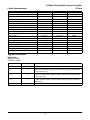
Table 5. Performance and Resource Utilization1
Slices
LUTs
Registers
sysMEM™
EBRs
fMAX (MHz)
With MIIM_module
1008
1428
1032
1
125(-5, -6) / 312.5(-7)
Without MIIM_module
1168
1606
1186
1
125(-5, -6) / 312.5(-7)
Mode
1. Performance and utilization characteristics are in Lattice’s ispLEVER 6.1 SP2 software and targeting an LFSCM3GA15EP1-5F256CES
device (1G data rate) or LFSCM3GA15EP1-7F256CES device (2.5Gbps data rate). When using this IP core in a different array size or
speed grade within the LatticeSC/M family or in a different software version, performance may vary.
Ordering Part Number
The Ordering Part Number (OPN) for the 2.5Gbps Ethernet Media Access Controller IP core targeting LatticeSC/M
devices is 2G5-MAC-SC-U1.
You can use the IPexpress software tool to help generate new configurations of this IP core. IPexpress is the Lattice
IP configuration utility, and is included as a standard feature of the ispLEVER design tools. Details regarding the
usage of IPexpress can be found in the IPexpress and ispLEVER help system. For more information on the
ispLEVER design tools, visit the Lattice website at: www.latticesemi.com/software.
28
2.5Gbps Ethernet Media Access Controller
IP Core
Lattice Semiconductor
Appendix – 2.5Gbps MAC Top-Level Reference Design
Included with the 2.5Gbps MAC IP core is a reference design that may be used as an example for how to instantiate, simulate, map, place and route the Lattice 2.5Gbps MAC IP core in an example working design. This reference
design uses the source files provided with the Gig-Speed Ethernet MAC IP core for instantiating the core. Scripts
for reading and configuring registers in the MAC and PCS/SERDES are included in this description.
Figure 17 shows an overall test application environment for the 2.5Gbps MAC core, using the LatticeSC/M
Advanced Evaluation Board and an Ethernet test set. Figure 18 is a pictorial representation of the reference design
FPGA top, which is the gig_mac_top.v file in the C:\<project_dir>\2g5mac_eval\<username>\src\rtl\top directory.
2.5Gbps MAC IP Core Overview
The four main interfaces to the 2.5Gbps MAC IP core include:
1. GMII Interface – This is the IEEE 802.3 standard Gigabit/Media Independent Interface that connects the MAC
to the PHY layer device (1Gbps) or PCS/SERDES (2.5 Gbps).
2. SMI Interface – This is the IEEE 802.3 Standard Serial Management Interface that connects to the PHY layer
device’s Management interface. This interface consists of the mdio, and mdc pins. Note that this interface is not
used in this 2.5 Gbps Test application, since the PHY is internal to the ASB portion of the FPGA and is accessed
via the SYSBUS.
3. Host Bus Interface – This is a Lattice-defined generic processor host bus that is needed to interface to the internal MAC registers. Note that in the test application design (Figure 18) the Host Bus interface is connected to the
JTAG ORCAstra interface and SYSBUS via some glue logic. More information on the ORCAstra Bus can be
found on the Lattice website.
4. MAC Rx/Tx Client Interface – This Lattice-defined generic interface consists of the following Rx/Tx FIFO interfaces, Rx/Tx Statistics interfaces and a few simple status and control bits.
Test Application Environment
The test application environment (Figure 17) Includes a LatticeSC/M Evaluation Board, and a PC with appropriate
cables and software (ORCAstra and ispVM® System software). A JTAG connection via the USB interface on the PC
is used to access the ORCAstra interface in the test application. The PHY (PCS/SERDES in ASB), MAC (IP core)
and test logic registers can all be configured and monitored via the ORCAstra/SYSBUS interface. In order to use
the test setup to send and receive looped back packets through the test application design the following steps need
to be performed:
1. Set up the LatticeSC/M Evaluation board, and PC as shown in Figure 17.
2. Program the LatticeSC/M device via the JTAG port and ispVM System software with the test application design.
3. Run the appropriate ORCAstra macro script to configure, test logic, MAC and PCS/SERDES registers (example
configurations are as is the test bench script).
4. Run traffic through the test setup and then run an ORCAstra macro script to dump test status and statistics registers.
Note: The driver sends a single Ethernet packet (from a ROM) with correct FCS repeatedly, within a fixed, deterministic time interval. The monitor checks for the same packet arrival. The external GMII port can be selected
with an external switch, but is intended primarily for simulation purposes, so that the user can verify sending and
receiving different Ethernet packets.
29
2.5Gbps Ethernet Media Access Controller
IP Core
Lattice Semiconductor
Figure 17. Test Application Environment
LatticeSC Evaluation Board
LatticeSC FPGA
SMI Not Used
2G5M
AC
LOOP
GMII
CHAN_0
PRIM
PCS/
SERDES
(8b10b)
REGS
SERDES
SYSBUS
MON
GMII
ORCAstra
DRV
JTAG
USB
(ORCAstra)
CHAN_0
SEC
SW1
GMII
PC
Test Application Design
The test application design (Figure 18) provides a loopback path for packets on the MAC Rx/Tx Client interface,
through a FIFO and associated logic. Ethernet packets are sourced to the Rx GMII (via the PCS/SERDES interface) and looped back on the MAC Rx/Tx Client FIFO interface. Note that the source and destination addresses in
the Ethernet frame can be swapped so the looped back packets on the Tx GMII have the correct source and destination addresses. Note: The packets on the primary PCS/SERDES (used by DUT) are driven by the driver ROM
circuit on the secondary PCS/SERDES. The test design also provides connections to all the other interfaces of the
Lattice 2.5Gbps MAC IP core, like the SMI (not used), Host Bus and Rx/Tx Statistics interfaces.
The main blocks and functions of the test application design are as follows:
Test Logic Module
This module includes the address swap logic, loopback FIFO and associated control logic, and miscellaneous control and status glue logic between the MAC Rx/Tx Client interface and the Register interface module. Figure 19
shows a timing waveform of data and control signals on the ingress and egress sides of the Address Swap Module
(when address swap is enabled).
The ORCAstra and SYSBUS Modules
These modules interface the ORCAstra Bus (a Lattice-defined slow speed serial bus) to the Host Bus (MAC registers), PCS slave interface (PCS registers) and a User Slave Interface bus (Test Logic registers). Using the ORCAs-
30
2.5Gbps Ethernet Media Access Controller
IP Core
Lattice Semiconductor
tra interface, a user can access the internal 2.5Gbps MAC core registers, the Test Application registers and the
PCS registers. The MAC registers (accessed via the Host Bus) and test logic registers (accessed via the USI) are
memory mapped as described in the Test Application Registers section. An ORCAstra Bus Test bench driver is provided to ease simulation with this interface.
Register Interface Module
This module is accessed through the ORCAstra Bus via the User Slave Interface (USI). The module contains registers used by the test application for control and status of the 2.5Gbps MAC core. In addition, this module contains
16-bit statistics counters fed by the 2.5Gbps MAC core’s Rx/Tx Statistics interfaces. These counters can be read
and cleared through the ORCAstra Bus. An address map and description of these registers is given in the Test
Application Registers section of this document.
Tx Driver
This module drives an Ethernet packet stored in memory (embedded RAM) to the secondary PCS’s GMII interface.
Two identical packets are continuously read out of the memory and sent with a fixed time interval between packets.
Note: for simulation purposes the GMII interface of the secondary PCS can either be driven by the output of the
driver circuit or an external GMII port. The external port is not expected to be driven in a actual implementation of
the test application design.
Rx Monitor
This module compares the packet returning from the looped back 2.5Gbps MAC client interface against what was
sent by the driver. If the packet does not match, a fail signal is asserted.
31
2.5Gbps Ethernet Media Access Controller
IP Core
Lattice Semiconductor
Figure 18. Test Application Reference Design
gmac_top.v
ref _clk _in (156.25 Mhz)
quad _clk (ref_clk_out – 312.5Mhz)
serdes_rx_clk
serdes_tx_clk
quad _clk (312.5 Mhz)
QUAD
pcs_serdes_left
PRI_CHAN_0
txd_pos
Hdout_n
Hdout_p
Hdin_n
Hdinp
txen
rxmac_clk
GMII
txer
txmac_clk
rx_dv_pos
reset_n
rx_er_pos
rxd_pos
FIFO
2048x9
8 tx_fifodata
TDI
tx_fifobyten
tx_fifoavail
fifo_wr
empty
TMS
Internal
Osc.
tx_fifoeof
tx_fifoempty
JTAG
PRI_CHAN_3
TCK
TDO
(x20 mode)
tx_sndpaustim
tx_sndpausreq
tx_fifoctrl
full
tx_staten
tx_macread
fifo_rd
2.5 Gbps MAC
IP Core
ORCAstra
Interface
tx_statvec
hclk
tx_done
tx_disfrm
Loopback
hcs_n
rx_fifo_full
haddr
rx_write
8
hdatain
rx_dbout
hdataout
Address
Swap
hread_n
rx_stat_en
hready_n
ignore_next_pkt
rx_eof
PCS/
SERDES
SYSBUS and
Glue logic
hwrite_n
rx_stat_vector
hdataout_en_n
us_size
us_addr
us_write
us_rdy
Register
Interface Module
(status/control regs and statistics counters)
Other reg cntl and status
Add_swap
loop_enb
Pin AG24 ext_gmii_sel
us_wdata
hclk
us_ack
rx_fifo_error
NULL
us_rdata
rx_error
QUAD
pcs_serdes_right
mux_sel
txd_ext, txen_txt, txer_ext
txd, txen, txer
SEC_CHAN_0
serdes_rx_clk
TX_DRIVER
ROM
Pass LED
Fail LED
Display
logic
rxd, rxdv, rxer
serdes_tx_clk
RX_MONITOR
Hdout_n
Hdout_p
Hdin_n
Hdinp
SEC_CHAN_3
quad _clk (312.5 Mhz)
(x20 mode)
32
2.5Gbps Ethernet Media Access Controller
IP Core
Lattice Semiconductor
Figure 19. Address Swap Module Data and Control Signals
rx_dbout
Dest.
Len/
Type
Source
DATA/PAD
FCS
rx_write
eof
rx_dbout
add_swap
rx_write_dly
Source
Len/
Type
Dest.
DATA/PAD
FCS
eof_dly
Test Application Test Bench
Figure 20 shows a block diagram of the test bench setup provided with the test application design. All accesses to
the internal 2.5Gbps MAC registers and test application design registers can be accomplished through the
testcase.v file (via the JTAG driver). In addition, variable sizes and types of Ethernet frames can be sourced to
the 2.5Gbps MAC Rx GMII via the Tx GMII port of the secondary PCS port through the testcase.v file (via the
Rx frame generator). Fixed packets can be sourced via the internal ROM packet driver. These received packets (at
the 2.5Gbps MAC Rx GMII) get looped back inside the test application design and through the 2.5Gbps MAC Tx
GMII and the primary PCS back to the secondary PCS to the monitor. The dashed line in Figure 20 shows this
loopback.
Figure 20. Test Application Reference Design Testbench Set-Up
MAC FIFO
tb .v
GMII
Client side
GMAC_top.v
Add Swap
& Loopback
Ref_clk_in
Ref_in
Tx
2.5Gbps
MAC
IP Core
Rx
Hdout(n/p)
Hdin(n/p)
Ref_out
HB
Register
Interface
PASS/FAIL
Statistics
Control &
Status
PCS/SERDES
SYSBUS
JTAG
JTAG Driver
testcase.v
ORCAstra
Interface
Hdin(n/p)
PKT Monitor
PKT Driver
ROM
Hdout(n/p)
Rx_frame
Generator
33
2.5Gbps Ethernet Media Access Controller
IP Core
Lattice Semiconductor
Test Application Registers
Two regions of SYSBUS memory space are used to configure and monitor the test application design. The first
address space is the region used to configure and monitor the PCS/SERDES. More information on the registers in
this address space can be found in the LatticeSC/M Family flexiPCS™ Data Sheet.
The second address space is the address space on the SYSBUS that is mapped to the User Slave Interface (USI).
Of the 190 KB of USI space, starting at 0x00800, only 256 B are used for the test application design. The 256 B
USI address space is carved in to four 64 B regions and is allocated as shown in Table 6.
The address space used by the 2.5Gbps MAC core internal registers as specified in this user’s guide are mapped
in the test application design is shown in Table 7.
Detailed descriptions of the register bits shown in Table 7 are given in this user’s guide.
Table 6. PCS Slave and 256B USI Address Space in Test Application Design
Register Description
Left PCS slave Interface
Base Offset
Start Add
End Add
0x30000
0x30000
0x364FF
Right PCS slave Interface
0x38000
0x38000
0x3E4FF
Inter-Quad PCS slave Interface
0x3EF00
0x3EF00
0x3EFFF
MAC IP core registers
0x00800 (CS_0)
0x800
0x83F (used up to 0x835)
Test Logic registers
0x00840 (CS_1)
0x840
0x87F (used up to 0x871)
ID/Scratch Pad registers
0x00880 (CS_2)
0x880
0x8BF (used up to 0x882)
Unused
0x008C0 (CS_3)
0x8C0
0x8FF (all 64B unused)
Table 7. 2.5Gbps MAC Internal Registers
Register Description
Mode register
Transmit and Receive Control register
Maximum Packet Size register
Inter Packet Gap register
Mnemonic
I/O Address
POR Value
MODE
800H - 801H
0000H
TX_RX_CTL
802H - 803H
0000H
MAX_PKT_SIZE
804H - 805H
05EEH
IPG_VAL
808H - 809H
0048H
2.5Gbps MAC Address register 0
MAC_ADDR_0
80AH - 80BH
0000H
2.5Gbps MAC Address register 1
MAC_ADDR_1
80CH - 80DH
0000H
2.5Gbps MAC Address register 2
MAC_ADDR_2
80EH - 80FH
0000H
TX_RX_STS
812H - 813H
0000H
Transmit and Receive Status
GMII Management Interface Control register
GMII_MNG_CTL
814H - 815H
0000H
GMII Management Data register
GMII_MNG_DAT
816H - 817H
0000H
VLAN Tag Length/type register
VLAN_TAG
832H - 833H
0000H
Multicast_table_0
MLT_TAB_0
822H - 823H
0000H
Multicast_table_1
MLT_TAB_1
824H - 825H
0000H
Multicast_table_2
MLT_TAB_2
826H - 827H
0000H
Multicast_table_3
MLT_TAB_3
828H - 829H
0000H
Multicast_table_4
MLT_TAB_4
82AH - 82BH
0000H
Multicast_table_5
MLT_TAB_5
82CH - 82DH
0000H
Multicast_table_6
MLT_TAB_6
82EH - 82FH
0000H
Multicast_table_7
MLT_TAB_7
830H - 831H
0000H
PAUS_OP
834H - 835H
0080H
Pause_opcode
34
2.5Gbps Ethernet Media Access Controller
IP Core
Lattice Semiconductor
The address space used by the Test Control Registers is shown in Table 8. This space contains ID, control, status
and statistics registers used by the test application.
The REGINTF logic block in the test application provides the address decoding, for the RO and R/W Registers
used by the tst_logic and statistics counters. All registers are eight bits wide and are addressable on byte
boundaries. Note that the statistics counter registers are composed of two 8-bit registers, a low and a high byte
register, therefore, in order to access these registers, two byte accesses must be made. For example, to access all
16 bits of the RXOKCNT would require an access to both 0x859 (high byte) and 0x858 (low byte). Note that since
the statistics counter registers are Clear On Read (COR), the high byte should be read first before reading the low
byte, since a read of the low byte clears all the combined 16 bits of the low and high registers. The address map for
the Test Application Related Resisters is as follows:
Table 8. Test Application Related Registers
Address
Register Description
0x0840
Version/IDentification Register
0x0841
Test Control Register
0x0842
Test Control Register 2
0x0843
0x0844
Mnemonic
Type
VERID
RO
TSTCNTL
RW
TSTCNTL_2
RW
MAC Control Register
MACCNTL
RW
Pause Timer Register - Low byte
PAUSTMRL
RW
0x0845
Pause Timer Register - High byte
PAUSTMRH
RW
0x0846
FIFO Almost Full Threshold Register - Low
FIFOAFTL
RW
0x0847
FIFO Almost Full Threshold Register - High
FIFOAFTH
RW
0x0848
FIFO Almost Empty Threshold Register - Low
FIFOAETL
RW
0x0849
FIFO Almost Empty Threshold Register - High
FIFOAETH
RW
0x084a
Rx Status Register
RXSTATUS
RO/COR
0x084b
Tx Status Register
TXSTATUS
RO/COR
0x084c, 0x084d
Rx Packet Ignored Counter Register (L,H)
RXPICNT
RO/COR
RXLCECNT
RO/COR
RXLFCNT
RO/COR
0x084e, 0x084f
Rx Length Check Error CouNTer (L,H)
0x0850, 0x0851
Rx Long Frames CouNTer Register (L,H)
0x0852, 0x0853
Rx Short Frames CouNTer Register (L,H)
RXSFCNT
RO/COR
0x0854, 0x0855
Rx IPG violations CouNTer Register (L,H)
RXIPGCNT
RO/COR
0x0856, 0x0857
Rx CRC errors CouNTer Register (L,H)
RXCRCCNT
RO/COR
0x0858, 0x0859
Rx OK packets CouNTer Register (L,H)
RXOKCNT
RO/COR
0x085a, 0x085b
Rx Control Frame CouNTer Register (L,H)
RXCFCNT
RO/COR
0x085c, 0x085d
Rx Pause Frame CouNTer Register (L,H)
RXPFCNT
RO/COR
0x085e, 0x085f
Rx Multicast Frame CouNTer Register (L,H)
RXMFCNT
RO/COR
0x0860, 0x0861
Rx Broadcast Frame CouNTer Register (L,H)
RXBFCNT
RO/COR
0x0862, 0x0863
Rx VLAN tagged Frame CouNTer Register (L,H)
RXVFCNT
RO/COR
0x0864, 0x0865
Tx Unicast Frame CouNTer Register (L,H)
TXUFCNT
RO/COR
0x0866, 0x0867
Tx Pause Frame CouNTer Register
0x0868, 0x0869
Tx Multicast Frame CouNTer Register (L,H)
(L,H)
TXPFCNT
RO/COR
TXMFCNT
RO/COR
0x086a, 0x086b
Tx Broadcast Frame CouNTer Register (L,H)
TXBFCNT
RO/COR
0x086c, 0x086d
Tx VLAN tagged Frame CouNTer Register (L,H)
TXVFCNT
RO/COR
0x086e, 0x086f
Tx BAD FCS Frame CouNTer Register (L,H)
0x0870, 0x0871
Tx Jumbo Frame CouNTer Register (L,H)
0x0872 - 0x08FF
UNUSED
35
TXBFCCNT
RO/COR
TXJFCNT
RO/COR
2.5Gbps Ethernet Media Access Controller
IP Core
Lattice Semiconductor
The ID/Scratch pad registers are a simple set of registers used for additional IDs and one register can be used as
a scratch Pad. Table 9 shows the registers.
Table 9. ID/Scratch Pad Registers
Address
Register Description
Mnemonic
Type
0x880
8 bit id_0
ID0
RO (0xAA)
0x881
8 bit Id_1
ID1
RO (0x55)
0x882
Scratch pad
scratch
R/W
0x882-0x8BF Unused
Unused
Register Bit Descriptions for Table 8.
0x0840 Version/IDentification Register VERID Read Only
default value = 0xA2
-------------------------------------------------------------------------------------------------------------------------0x0841 Test Control Register
TSTCNTL Read/Write
default value = 0x00
bit_0 = destination/source address swap - 1 = swap, 0 = no swap
bit_1 = loop back enable - 1 = loopback, 0 = no loopback
bit_2 = Not used
bit_3 = Not used
bit_4 = Not used
bit_5 = Not used
bit_6 = Not used
bit_7 = Not used
-------------------------------------------------------------------------------------------------------------------------0x0842 Test Control Register 2
TSTCNTL 2 Read/Write
default value = 0x00
bit_0 = Not used
bit_1 = Not used
bit_2 = Not used
bit_3 = Not used
bit_4 = Not used
bit_5 = Not used
bit_6 = Not used
bit_7 = Not used
-------------------------------------------------------------------------------------------------------------------------0x0843 MAC Control Register
MACCNTL Read/Write
default value = 0x00
bit_0 = send pause request: 1 = send request, 0 = don’t send request
This register bit gets ORed with the tx_fifo almost full signal. The ORed output sets the
tx_sndpausreq pin on the 2.5Gbps MAC core.
bit_1 = fifo control frame
This register bit sets the tx_fifoctrl pin on the 2.5Gbps MAC core.
36
2.5Gbps Ethernet Media Access Controller
IP Core
Lattice Semiconductor
bit_2 = rx_fifo full (Note that the Tx and Rx FIFO are the same, only one loopback FIFO).
This register bit gets ORed with the tx_fifo full signal. The ORed output sets the rx_fifo_full pin on
the 2.5Gbps MAC core. See the LatticeSC/M Family Data Sheet for more information. Note that by setting
this bit you can mimic the Rx FIFO being full.
bit_3 = tx_fifo empty
This register bit gets ORed with the tx_fifo empty signal. The ORed output sets the tx_fifo_empty
pin on the 2.5Gbps MAC core. See the LatticeSC/M Family Data Sheet for more information. Note that by
setting this bit you can mimic the Tx FIFO being empty.
bit_4 = ignore next packet
This register bit sets the ignore_next_pkt pin on the 2.5Gbps MAC core.
bit_5 = Not used
bit_6 = Not used
bit_7 = Not used
-------------------------------------------------------------------------------------------------------------------------0x0844 Pause Timer Register - Low byte
PAUSTMRL Read/Write
0x0845 Pause Timer Register - High byte
PAUSTMRH Read/Write
default value = 0x0000
Low Reg
bit[7:0] = pause timer low bits
These register bits set the tx_sndpaustim[7:0] pins on the 2.5Gbps MAC core.
High Reg
bit[7:0] = pause timer high bits
These register bits set the tx_sndpaustim[15:8] pins on the 2.5Gbps MAC core.
-------------------------------------------------------------------------------------------------------------------------0x0846 FIFO Almost Full Threshold Register - Low
FIFOAFTL Read/Write
0x0847 FIFO Almost Full Threshold Register - High FIFOAFTH Read/Write
default value = 0x01C1
Low Reg
bit[7:0] = FIFO Almost Full Threshold - Low
These register bits set the loopback FIFO threshold [7:0] bits.
High Reg
bit[0] =
FIFO Almost Full Threshold - High
This register bit sets the loopback FIFO threshold bit [8].
bit[7:1] = Not used.
-------------------------------------------------------------------------------------------------------------------------0x0848 FIFO Almost Empty Threshold Register - Low
FIFOAETL Read/Write
0x0849 FIFO Almost Empty Threshold Register - High FIFOAETH Read/Write
default value = 0x0005
Low Reg
bit[7:0] = FIFO Almost Empty Threshold - Low
These register bits set the loopback FIFO threshold [7:0] bits.
37
2.5Gbps Ethernet Media Access Controller
IP Core
Lattice Semiconductor
High Reg
bit[0] = FIFO Almost Empty Threshold - High
This register bit sets the loopback FIFO threshold bit [8].
bit[7:1] = Not used.
0x084a Rx Status Register
default value = 0x00
0x084b Tx Status Register
default value = 0x00
RXSTATUS Read Only/clear on read
TXSTATUS Read Only/clear on read
Rx status
bit_0 = latches rx_error value from 2.5Gbps MAC core pin
bit_1 = latches rx_fifo_error value from 2.5Gbps MAC core pin
bit_2 = Not Used
bit_3 = Not used
bit_4 = Not used
bit_5 = Not used
bit_6 = Not used
bit_7 = Not used
Tx status
bit_0 = latches tx_discfrm value from 2.5Gbps MAC core pin
bit_1 = latches tx_fifo_full value from loopback fifo
bit_2 = Not Used
bit_3 = Not used
bit_4 = Not used
bit_5 = Not used
bit_6 = Not used
bit_7 = Not used
-------------------------------------------------------------------------------------------------------------------------The following counter registers are all 16 bits with 8-bit low and 8-bit high address locations. The counters count
different Rx and Tx statistics as defined by the statistics vectors in this document. All counters have a power-on
default value of 0x0000.
0x084c
0x084e
0x0850
0x0852
0x0854
0x0856
0x0858
0x085a
0x085c
0x085e
0x0860
0x0862
Rx Packet Ignored Counter Register
Rx Length Check Error Counter
Rx Long Frames Counter Register
Rx Short Frames Counter Register
Rx IPG violations Counter Register
Rx CRC errors Counter Register
Rx OK packets Counter Register
Rx Control Frame Counter Register
Rx Pause Frame Counter Register
Rx Multicast Frame Counter Register
Rx Broadcast Frame Counter Register
Rx VLAN Tagged Frame Counter Register
RXPICNT
RXLCECNT
RXLFCNT
RXSFCNT
RXIPGCNT
RXCRCCNT
RXOKCNT
RXCFCNT
RXPFCNT
RXMFCNT
RXBFCNT
RXVFCNT
RO/COR
RO/COR
RO/COR
RO/COR
RO/COR
RO/COR
RO/COR
RO/COR
RO/COR
RO/COR
RO/COR
RO/COR
0x0864
0x0866
0x0868
0x086a
0x086c
0x086e
0x0870
Tx Unicast Frame Counter Register
Tx Pause Frame Counter Register
Tx Multicast Frame Counter Register
Tx Broadcast Frame Counter Register
Tx VLAN Tagged Frame Counter Register
Tx BAD FCS Frame Counter Register
Tx Jumbo Frame Counter Register
TXUFCNT
TXPFCNT
TXMFCNT
TXBFCNT
TXVFCNT
TXBFCCNT
TXJFCNT
RO/COR
RO/COR
RO/COR
RO/COR
RO/COR
RO/COR
RO/COR
38
2.5Gbps Ethernet Media Access Controller
IP Core
Lattice Semiconductor
Test Application Pins
Table 10. Test Application FPGA Pins
I/O
Pin Number
ref_clk_in
Signal Name
In
N27
Reference Clock - 156.25MHz clock source
Signal Description
rst_n
In
H5
Reset - Active low global reset
hdinp0
In
HDINP00
Inbound SERDES P - Channel 0
Inbound SERDES N - Channel 0
hdinn0
In
HDINN00
hdoutp0
Out
HDOUTP00
hdoutn0
Out
HDOUTN00
hdinp1
In
HDINP10
Inbound SERDES P - Channel 1
Inbound SERDES N - Channel 1
Outbound SERDES P - Channel 0
Outbound SERDES N - Channel 0
hdinn1
In
HDINN10
hdoutp1
Out
HDOUTP10
hdoutn1
Out
HDOUTN10
In
TCK
JTAG Clock Source (0 - 50MHz)
tck
Outbound SERDES P - Channel 1
Outbound SERDES N - Channel 1
tdi
In
TDI
JTAG Data Input
tdo
Out
TDO
JTAG Data Output
tms
In
TMS
JTAG Test Mode Select
activity_dut_LED
Out
U26
Blue LED flashes when RX_DV on Channel 0 toggles
activity_drv_chan_LED
Out
H26
ORANGE LED flashes when RX_DV on Channel 1 toggles
mon_pass_LED
Out
AD25
Yellow LED solid on when Channel1 monitor data pattern
OK
mon_fail_LED
Out
AJ28
Red LED solid on when Channel 1 monitor data pattern fails
ext_gmii_sel
In
AG24
Set low to source packets from internal packet driver
Note: Location preferences are not specified for these pins. See your implementation results for actual pin locations.
39