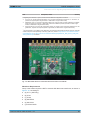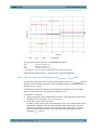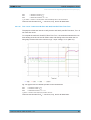
1
R&S®RTO-K26
D-PHY Compliance Test
Test Procedures
(=J::2)
Test Procedures
Test & Measurement
1326.1010.02 ─ 02
This manual describes the D-PHY compliance test procedures with the following option:
●
R&S®RTO-K26 (1317.5668.02) - D-PHY
The tests require the R&S ScopeSuite software.
© 2014 Rohde & Schwarz GmbH & Co. KG
Mühldorfstr. 15, 81671 München, Germany
Phone: +49 89 41 29 - 0
Fax: +49 89 41 29 12 164
E-mail: [email protected]
Internet: www.rohde-schwarz.com
Subject to change – Data without tolerance limits is not binding.
R&S® is a registered trademark of Rohde & Schwarz GmbH & Co. KG.
Trade names are trademarks of the owners.
The following abbreviations are used throughout this manual: R&S®RTO is abbreviated as R&S RTO, and R&S®ScopeSuite is
abbreviated as R&S ScopeSuite.
R&S®RTO-K26
Contents
Contents
1 Preparing the Measurements................................................................5
1.1
Test Equipment............................................................................................................. 5
1.2
Installing Software and License.................................................................................. 5
1.3
Setting Up the Network.................................................................................................6
1.4
Starting the R&S ScopeSuite....................................................................................... 7
1.5
Connecting the R&S RTO.............................................................................................7
2 Performing Tests..................................................................................10
2.1
Configuring the Test................................................................................................... 10
2.1.1
General Test Settings................................................................................................... 11
2.2
Controlling Test Cycles.............................................................................................. 12
2.3
Getting Test Results................................................................................................... 13
3 D-PHY Compliance Tests.................................................................... 15
3.1
Starting D-PHY Compliance Tests.............................................................................17
3.2
Test Configuration for D-PHY.................................................................................... 18
3.3
Data Lane LP-TX Signaling Requirements (Group 1).............................................. 21
3.3.1
Test Setup.....................................................................................................................21
3.3.2
Performing Group 1 Test Cases................................................................................... 23
3.3.3
Measurements.............................................................................................................. 24
3.4
Clock Lane LP-TX Signaling Requirements (Group 2)............................................ 31
3.4.1
Test Setup.....................................................................................................................31
3.4.2
Performing Group 2 Test Cases................................................................................... 32
3.4.3
Measurements.............................................................................................................. 34
3.5
Data Lane HS-TX Signaling Requirements (Group 3).............................................. 40
3.5.1
Test Setup.....................................................................................................................40
3.5.2
Performing Group 3 Test Cases................................................................................... 44
3.5.3
Measurements.............................................................................................................. 45
3.6
Clock Lane HS-TX Signaling Requirements (Group 4)............................................ 62
3.6.1
Test Setup.....................................................................................................................63
3.6.2
Performing Group 4 Test Cases................................................................................... 67
3.6.3
Measurements.............................................................................................................. 68
3.7
HS-TX Clock-to-Data Lane Timing Requirements (Group 5)...................................88
Test Procedures 1326.1010.02 ─ 02
3
R&S®RTO-K26
Contents
3.7.1
Test Setup.....................................................................................................................89
3.7.2
Performing Group 5 Test Cases................................................................................... 91
3.7.3
Measurements.............................................................................................................. 93
Test Procedures 1326.1010.02 ─ 02
4
R&S®RTO-K26
Preparing the Measurements
Test Equipment
1 Preparing the Measurements
1.1 Test Equipment
For D-PHY compliance tests, the following test equipment is needed:
●
R&S RTO oscilloscope with 4 channels and at least 4 GHz bandwidth R&S RTO1044 or equivalent; alternatively R&S RTO1004/1014/1024 with bandwidth extension 4 GHz (R&S RTO-B202/-B204/-205)
●
For measuring the clock signal (+ and -): either 1 differential probe or 2 singleended probes with at least 4 GHz bandwidth (R&S RT‑ZD40 or R&S RT‑ZS60).
However, note that D-PHY Group 2 and Group 4 tests require 2 probes for the
clock signal.
●
For measuring the data signal (+ and -): 2 probes with at least 4 GHz bandwidth
(either 2 R&S RT‑ZD40 or 2 R&S RT‑ZS60)
●
R&S RTO-K26 D-PHY compliance test option (required option, installed on the
R&S RTO)
●
Recommended test fixture for LP-TX tests: MIPI D-PHY Capacitive Load (CLOAD)
Fixture from The University of New Hampshire InterOperability Laboratory (UNHIOL)
●
Recommended termination board for HS-TX tests: MIPI D-PHY Reference Termination Board (RTB) from The University of New Hampshire InterOperability Laboratory (UNH-IOL)
●
The free-of-charge R&S ScopeSuite software requires the Windows 7 operating
system. It can be installed on a computer or directly on the R&S RTO if the instrument has Windows 7.
1.2 Installing Software and License
The preparation steps have to be performed only once for each computer and instrument that are used for testing.
Uninstall older versions of the R&S ScopeSuite
If an older version of the R&S ScopeSuite is installed, make sure to uninstall the old
version before you install the new one. You can find the version number of the current
installation in "Help" menu > "About". To unistall the R&S ScopeSuite, use the Windows Control Panel > "Programs".
Test Procedures 1326.1010.02 ─ 02
5
R&S®RTO-K26
Preparing the Measurements
Setting Up the Network
To install the R&S ScopeSuite
1. Download the R&S ScopeSuite software from the "Downloads > Software" section
on the Rohde & Schwarz "Scope of the Art" web page: www.scope-of-the-art.com/
product/rto.html.
2. Install the R&S ScopeSuite software:
●
●
Either on the computer that is used for testing,
or on the R&S RTO if the instrument has a Windows 7 operating system.
To install the license key on the R&S RTO
► When you got the license key of the compliance test option, enable it on the
R&S RTO using SETUP > "SW Options".
For a detailed description, refer to the R&S RTO User Manual, chapter "Installing
Options", or to the online help on the instrument.
1.3 Setting Up the Network
If the R&S ScopeSuite software runs on a test computer, the computer and the testing
R&S RTO require a LAN connection.
For some test cases, you need an additional instrument (arbitrary waveform generator
(ARB), vector network analyzer (VNA), or spectrum analyzer. These instruments can
be used in automatic or manual mode. For automatic testing, a LAN connection to the
additional instrument is required.
There are two ways of connection:
●
LAN (local area network): It is recommended that you connect to a LAN with DHCP
server. This server uses the Dynamic Host Configuration Protocol (DHCP) to
assign all address information automatically.
If no DHCP server is available, or if the Tabor WX2182B is used for automatic testing, assign fixed IP adresses to all devices.
●
Direct connection of the instruments and the computer or connection to a switch
using LAN cables: Assign fixed IP addresses to the computer and the instruments
and reboot all devices.
To set up and test the LAN connection
1. Connect the computer and the instruments to the same LAN.
2. Start all devices.
3. If no DHCP server is available, assign fixed IP addresses to all devices.
4. Ping the instruments to make sure that the connection has been established.
5. If VISA is installed, check if VISA can access the instruments:
a) Start VISA on the test computer.
b) Validate the VISA address string of each device.
Test Procedures 1326.1010.02 ─ 02
6
R&S®RTO-K26
Preparing the Measurements
Starting the R&S ScopeSuite
See also:
●
chapter 1.5, "Connecting the R&S RTO", on page 7
1.4 Starting the R&S ScopeSuite
To start the R&S ScopeSuite on the test computer or on the oscilloscope:
► Double-click the R&S ScopeSuite program icon.
To start the R&S ScopeSuite on the instrument, in the R&S RTO firmware:
► On the "Analysis" menu, tap "Start Compliance Test".
1.5 Connecting the R&S RTO
If the R&S ScopeSuite is installed directly on the instrument, the software detects the
R&S RTO firmware automatically, and the "Oscilloscope" tab is not available in the
R&S ScopeSuite.
If the R&S ScopeSuite software runs on a test computer, the computer and the testing
R&S RTO require a LAN connection, see chapter 1.3, "Setting Up the Network",
on page 6. The R&S ScopeSuite software needs the IP address of the R&S RTO to
establish connection.
1. Start the R&S RTO.
2. Start the R&S ScopeSuite software.
3. Click "Instrument Settings".
Test Procedures 1326.1010.02 ─ 02
7
R&S®RTO-K26
Preparing the Measurements
Connecting the R&S RTO
4. Click the "Oscilloscope" tab.
5. Enter the IP address of the R&S RTO.
To obtain the IP address: Press the SETUP key on the instrument and tap the
"System" tab.
6. Click "Get Instrument Information".
The computer connects with the instrument and gets the instrument data.
Test Procedures 1326.1010.02 ─ 02
8
R&S®RTO-K26
Preparing the Measurements
Connecting the R&S RTO
If the connection fails, an error message is shown.
7. Click "Save".
Test Procedures 1326.1010.02 ─ 02
9
R&S®RTO-K26
Performing Tests
Configuring the Test
2 Performing Tests
2.1 Configuring the Test
1. In the R&S ScopeSuite window, select the compliance test to be performed:
●
"D-PHY"
2. Click "Configuration".
3. Click the "User Input" tab and enter common information on the test. See:
●
chapter 2.1.1.1, "User Input", on page 11
4. Click the "LP Configuration" and "HS Configuration" tabs. Then, for each of them:
5. Check and adjust the configuration settings. See:
●
chapter 3.2, "Test Configuration for D-PHY", on page 18
6. Select the "Report Configuration" tab to define the format and contents of the
report. See:
●
chapter 2.1.1.2, "Report Configuration", on page 11
7. Click "OK".
8. Click "Limit Editor".
Test Procedures 1326.1010.02 ─ 02
10
R&S®RTO-K26
Performing Tests
Configuring the Test
9. Select the "Test Type" in the lower left corner of the dialog box and check the measurement limits. See:
●
chapter 2.1.1.3, "Limit Editor", on page 12
10. Click "Start Test" and proceed as descibed in the relevant test case chapter.
2.1.1 General Test Settings
2.1.1.1
User Input
On the "User Input" tab, you enter common information on the test.
This information is written to the test report in section "General Information".
2.1.1.2
Report Configuration
On the "Report Configuration" tab, you select the format of the report and the details to
be included in the report. Here you can also select an icon that will be displayed in the
upper left corner of the report.
Test Procedures 1326.1010.02 ─ 02
11
R&S®RTO-K26
Performing Tests
Controlling Test Cycles
2.1.1.3
Limit Editor
The Limit Editor shows the measurement limits that are used for compliance testing.
Each limit comprises the comparison criterion, the unit, the limit value A, and a second
limit value B if the criterion requires two limits.
You can set the values to defaults, change the values in the table, export the table in
xml format, or import xml files with limit settings.
1. Select the "Test Type" in the lower left corner of the dialog box
2. Check and adjust the measurement limits.
2.2 Controlling Test Cycles
If you have selected several test cases or test case groups, and the test mode "Allow
Skip / Repeat" is set in the "Configuration" dialog box, you can control the test cycle.
After each completed test, its results are displayed in the "Test Case Result" dialog
box:
Test Procedures 1326.1010.02 ─ 02
12
R&S®RTO-K26
Performing Tests
Getting Test Results
Here you decide how to continue the test cycle:
Repeat Keep Previous
Repeats the test case and writes the results to the measurement report as often as
required. Use this function for debugging during develeopment and for stability tests
after interface integration.
Repeat Discard Previous
Deletes the measurement results and repeats the test case. Use this function if operating errors occured.
Next
Finishes the test case, writes the results to the measurement report and goes to the
next test case of the test cycle.
Abort
Cancels the test cycle and returns to the start window of the test.
2.3 Getting Test Results
For each test, the test data - report, diagrams and waveform files - is saved in the following folder:
Test Procedures 1326.1010.02 ─ 02
13
R&S®RTO-K26
Performing Tests
Getting Test Results
%ProgramData%\Rohde-Schwarz\RSScopeSuite\Sessions\
<Protocolgroup>\<Protocol>\<Session_Name>.
If you resume an existing session, new measurements are appended to the report,
new diagrams and waveform files are added to the session folder. Existing files are not
deleted or replaced. Sessions data remain until you delete them in the "Report Management" dialog box.
The report format and content is configured in "Test Configuration" > "Report Configuration". All reports are listed in the "Report Management" dialog box. Reports can be
provided in PDF, RTF, or HTML format. To view and print PDF reports, you need a
PDF viewer, for example, the Acrobat Reader.
The configured report file can be created directly at the end of the test cycle, or later in
the "Report Management" dialog box.
To show a test report
1. In the R&S ScopeSuite window, select the compliance test to be performed.
2. Click "Report Management".
3. Select the session name in the "Reports" list and click "Show".
4. If the report has not yet been generated, a message box asks if you want to create
the report.
Click "Yes".
The report opens in a separate application window, depending on the file format.
You can check the test results and print the report.
To delete the report, diagrams and waveform files of a session
1. In the "Report Management" dialog box, select the session name to be deleted.
2. Click "Remove".
To change the session name
1. In the "Report Management" dialog box, select the session name.
2. Click "Rename".
Test Procedures 1326.1010.02 ─ 02
14
R&S®RTO-K26
D-PHY Compliance Tests
3 D-PHY Compliance Tests
D-PHY Ethernet compliance tests require option R&S RTO-K26.
The software closely follows the MIPI Alliance's Conformance Test Suite for D-PHY
Physical Layer Version 1.1 Revision 03, dated June 5th, 2013. Should anything
remain unclear in this manual, please refer to that CTS document, which is available
for members of the MIPI Alliance at https://members.mipi.org/wg/All-Members/home/
approved-specs.
Table 3-1: Overview of D-PHY compliance tests
Test Groups and Tests
see
Group 1 (7 tests): Data Lane LP-TX Signaling Requirements
page
21
1.1.1 – Data Lane LP-TX Thevenin Output High Level Voltage (VOH)
1.1.2 – Data Lane LP-TX Thevenin Output Low Level Voltage (VOL)
1.1.3 – Data Lane LP-TX 15%-85% Rise Time (TRLP)
1.1.4 – Data Lane LP-TX 85%-15% Fall Time (TFLP)
1.1.5 – Data Lane LP-TX Slew Rate vs. CLOAD (δV/δtSR)
1.1.6 – Data Lane LP-TX Pulse Width of Exclusive-OR Clock (TLP-PULSE-TX)
1.1.7 – Data Lane LP-TX Period of Exclusive-OR Clock (TLP-PER-TX)
Group 2 (5 tests): Clock Lane LP-TX Signaling Requirements
1.2.1 – Clock Lane LP-TX Thevenin Output High Level Voltage (VOH)
page
31
1.2.2 – Clock Lane LP-TX Thevenin Output Low Level Voltage (VOL)
1.2.3 – Clock Lane LP-TX 15%-85% Rise Time (TRLP)
1.2.4 – Clock Lane LP-TX 85%-15% Fall Time (TFLP)
1.2.5 – Clock Lane LP-TX Slew Rate vs. CLOAD (δV/δtSR)
Group 3 (16 tests): Data Lane HS-TX Signaling Requirements
1.3.1 – Data Lane HS Entry: Data Lane TLPX Value
page
40
1.3.2 – Data Lane HS Entry: Data Lane THS-PREPARE Value
1.3.3 – Data Lane HS Entry: Data Lane THS-PREPARE + THS-ZERO Value
1.3.4 – Data Lane HS-TX Differential Voltages VOD(0) and VOD(1)
1.3.5 – Data Lane HS-TX Differential Voltage Mismatch ΔVOD
1.3.6 – Data Lane HS-TX Single-Ended Output Voltages VOHHS(DP) and VOHHS(DN)
1.3.7 – Data Lane HS-TX Static Common-Mode Voltages VCMTX(1) and VCMTX(0)
1.3.8 – Data Lane HS-TX Static Common-Mode Voltage Mismatch ΔVCMTX(1,0)
1.3.9 – Data Lane HS-TX Dynamic Common-Level Variations Between 50-450 MHz ΔVCMTX(LF)
1.3.10 – Data Lane HS-TX Dynamic Common-Level Variations Above 450 MHz ΔVCMTX(HF)
1.3.11 – Data Lane HS-TX 20%-80% Rise Time tR
1.3.12 – Data Lane HS-TX 80%-20% Fall Time tF
1.3.13 – Data Lane HS Exit: THS-TRAIL Value
1.3.14 – Data Lane HS Exit: 30%-85% Post-EoT Rise Time TREOT
1.3.15 – Data Lane HS Exit: TEOT Value
1.3.16 – Data Lane HS Exit: THS-EXIT Value
Test Procedures 1326.1010.02 ─ 02
15
R&S®RTO-K26
D-PHY Compliance Tests
Test Groups and Tests
see
Group 4 (18 tests): Clock Lane HS-TX Signaling Requirements
page
62
1.4.1 – Clock Lane HS Entry: TLPX Value
1.4.2 – Clock Lane HS Entry: TCLK-PREPARE Value
1.4.3 – Clock Lane HS Entry: TCLK-PREPARE + TCLK-ZERO Value
1.4.4 – Clock Lane HS-TX Differential Voltages VOD(0) and VOD(1)
1.4.5 – Clock Lane HS-TX Differential Voltage Mismatch ΔVOD
1.4.6 – Clock Lane HS-TX Single-Ended Output Voltages VOHHS(DP) and VOHHS(DN)
1.4.7 – Clock Lane HS-TX Static Common-Mode Voltages VCMTX(1) and VCMTX(0)
1.4.8 – Clock Lane HS-TX Static Common-Mode Voltage Mismatch ΔVCMTX(1,0)
1.4.9 – Clock Lane HS-TX Dynamic Common-Level Variations Between 50-450 MHz ΔVCMTX(LF)
1.4.10 – Clock Lane HS-TX Dynamic Common-Level Variations Above 450 MHz ΔVCMTX(HF)
1.4.11 – Clock Lane HS-TX 20%-80% Rise Time tR
1.4.12 – Clock Lane HS-TX 80%-20% Fall Time tF
1.4.13 – Clock Lane HS Exit: TCLK-TRAIL Value
1.4.14 – Clock Lane HS Exit: 30%-85% Post-EoT Rise Time TREOT
1.4.15 – Clock Lane HS Exit: TEOT Value
1.4.16 – Clock Lane HS Exit: THS-EXIT Value
1.4.17 – Clock Lane HS Clock Instantaneous: UIINST Value
1.4.18 – Clock Lane HS Clock Delta UI: (ΔUI) Value
Group 5 (4 tests): HS-TX Clock-to-Data Lane Timing Requirements
1.5.1 – HS Entry: TCLK-PRE Value
page
88
1.5.2 – HS Exit: TCLK-POST Value
1.5.3 – HS Clock Rising Edge Alignment to First Payload Bit
1.5.4 – Data-to-Clock Skew (TSKEW[TX])
Any D-PHY configuration consists of at least one clock lane module, and one or several data lane modules. Each module provides a synchronized connection between
master and slave. During normal operation, a lane switches between the modes "low
power" (LP) and "high speed" (HS). High speed functions are used for HS data transmission in bursts with an arbitrary number of payload data bytes. Low power functions
are mainly used for control, but have other optional use cases, like LP escape mode.
The presence of HS and LP functions is correlated.
●
●
●
●
●
●
●
Starting D-PHY Compliance Tests..........................................................................17
Test Configuration for D-PHY................................................................................. 18
Data Lane LP-TX Signaling Requirements (Group 1).............................................21
Clock Lane LP-TX Signaling Requirements (Group 2)........................................... 31
Data Lane HS-TX Signaling Requirements (Group 3)............................................ 40
Clock Lane HS-TX Signaling Requirements (Group 4)...........................................62
HS-TX Clock-to-Data Lane Timing Requirements (Group 5)..................................88
Test Procedures 1326.1010.02 ─ 02
16
R&S®RTO-K26
D-PHY Compliance Tests
Starting D-PHY Compliance Tests
3.1 Starting D-PHY Compliance Tests
Before you run the test, complete the following actions:
●
Initial setup of the equipment, see chapter 1.2, "Installing Software and License",
on page 5
●
LAN connection of the oscilloscope and the computer running the R&S ScopeSuite, see chapter 1.5, "Connecting the R&S RTO", on page 7
1. Select "D-PHY" in the R&S ScopeSuite start window.
2. Check the test configuration settings and adjust, if necessary. See:
●
●
●
chapter 2.1.1.1, "User Input", on page 11
chapter 2.1.1.3, "Limit Editor", on page 12
chapter 3.2, "Test Configuration for D-PHY", on page 18
Specific information on the required settings is given in the "Test Requirements" chapters for each test group.
3. Click "Start Test".
4. In the "Test Management" dialog box, select the session and click "Next":
●
●
To start a new test session, select "New" and enter the session name.
To resume an existing test session, select "Resume Existing" and select the
session name.
5. In the "D-PHY Test" dialog box, select one or more groups of test cases as described in the relevant test case chapter.
Note: By selecting a group, all test cases of that group are selected. It is not possible to select individual test cases.
To view all test cases of a group, click on the little triangle on the left of the group
name.
Test Procedures 1326.1010.02 ─ 02
17
R&S®RTO-K26
D-PHY Compliance Tests
Test Configuration for D-PHY
3.2 Test Configuration for D-PHY
The test configuration consists of the general configuration settings as described in
chapter 2.1, "Configuring the Test", on page 10, and some additional test-specific configuration settings, described below:
●
"LP Configuration" for DUT lanes in low power (LP) mode
●
"HS Configuration" for DUT lanes in high speed (HS) mode
Fig. 3-1: LP Configuration for D-PHY compliance test cases, Groups 1 and 2
Select the "LP Configuration" tab for Group 1 and 2 test cases configuration of:
●
"Test Mode"
●
"Data Lane Under Test"
●
"CLOAD"
●
"Use Previous Settings"
●
"Low Pass Filter"
●
"Export Waveform"
Test Procedures 1326.1010.02 ─ 02
18
R&S®RTO-K26
D-PHY Compliance Tests
Test Configuration for D-PHY
Fig. 3-2: HS Configuration for D-PHY compliance test cases, Groups 3, 4 and 5
Select the "HS Configuration" tab for Group 3, 4 and 5 test cases configuration of:
●
"Test Mode"
●
"Data Lane Under Test"
●
"ZID"
●
"Clock Format"
●
"Use Previous Settings"
●
"DUT"
●
"Bitrate"
●
"Clock Type"
●
"Export Waveform"
Some fields are shared between "HS Configuration" and "LP Configuration", as well as
other compliance tests in R&S ScopeSuite
Test Mode
This is only applicable if multiple groups of test cases shall be executed.
● Select "Allow Skip / Repeat" to receive, at the end of each test execution, the
choice to repeat or skip a test case.
● Otherwise select "Do Not Allow Skip / Repeat".
For more details on the effects of this selection, see chapter 2.2, "Controlling Test
Cycles", on page 12.
Test Procedures 1326.1010.02 ─ 02
19
R&S®RTO-K26
D-PHY Compliance Tests
Test Configuration for D-PHY
Data Lane Under Test
Select the data lane number to be tested. This selection is only applicable for Group 1
test cases. Default selection is data lane "0".
CLOAD
● If a CLOAD test fixture with 50 pF termination capacitance is used, as required in the
MIPI Alliance Specification for D-PHY, version 1.1, select "50 pF".
● If the 50 pF CLOAD fixture is removed, select "Open".
Note: Test results are then reported as "Informative".
Be aware that the test results may not be valid, if no CLOAD test fixture with 50 pF termination capacitance is used. The optional "Open" configuration setting is used to provide a qualitative estimate of the amount of CLOAD contributed by the DUT's PCB.
ZID
The software supports all three cases of terminations, ZID:
● (a) 100 ohms (nominal load)
● (b) 80 ohms (minimum load)
● (c) 125 ohms (maximum load)
Specify the termination which is applied to the DUT. This selection is only applicable
for Group 3 and 4 test cases.
Clock Format
● Select "Single-Ended" if using two single-ended probes (or two differential probes
in single-ended mode) for the clock lane.
● Select "Differential" if using one differential probe for the clock lane.
This selection is only applicable for Group 3 and 5 test cases.
Use Previous Settings
Check this if you want to use the previous settings (which include trigger conditions,
vertical scale and horizontal time scale) for a new execution of the same group of test
cases with the same configurations.
If this is not checked, the software will...
● in case of LP configuration: ...use the pre-defined trigger conditions, vertical scale
and horizontal time scale.
● in case of HS configuration: ...go through a set of pre-defined routines to determine
the best trigger conditions and horizontal time scale.
DUT
Defines if the DUT is a camera (CSI-2) or display (DSI).
Bitrate ← DUT
If the bitrate of the DUT is known, enable "Bitrate" and enter the bitrate value in Mbps.
This is useful if the signal is noisy. This selection is only applicable for Group 3 test
cases.
Test Procedures 1326.1010.02 ─ 02
20
R&S®RTO-K26
D-PHY Compliance Tests
Data Lane LP-TX Signaling Requirements (Group 1)
Clock Type ← Bitrate ← DUT
If the DUT has a burst or non-continuous clock, select "Normal Burst". If the DUT has a
partial burst clock, select "HS Entry and Exit". If the DUT has a continuous clock, select
"All Continuous".
Low Pass Filter
If "Low Pass Filter" is enabled, the software applies a 4th order Butterworth low pass
filter with a cutoff frequency of 400 MHz to the input signal, as required in the MIPI Alliance Specification for D-PHY, version 1.1. Keep this option enabled, as some measurements are very sensitive to high-frequency noise.
Export Waveform
Enable "Export Waveform" to export the captured waveforms. The exported waveform
files are stored in the current session folder in
%ProgramData%\Rohde-Schwarz\RSScopeSuite\Sessions\DPHY\D-PHY\
<Session_Name>.
3.3 Data Lane LP-TX Signaling Requirements (Group 1)
The purpose of Group 1 test cases is to verify various requirements specific to data
lane low power (LP) signaling.
Group 1 consists of seven test cases, described in chapter 3.3.3, "Measurements",
on page 24. They perform related LP-TX measurements on a single data lane LP
transmit waveform sequence.
The software is intended to facilitate the execution of a set of LP-TX measurements on
a pair of captured LP data lane waveforms with ULPS Entry sequence.
These test cases are typically performed on CSI-2 and DSI Master devices, only.
3.3.1 Test Setup
Table 3-2: Equipment for Group 1 Data Lane LP-TX Signaling Requirements test
Item
Description, model
Quantity
Rohde & Schwarz oscilloscope
R&S RTO1044 or equivalent (4 GHz)
1
Probes
Differential probes: R&S RT‑ZD40, or
2 (*)
Single-ended probes: R&S RT‑ZS60
Test fixture
UNH-IOL MIPI D-PHY Capacitive Load (CLOAD)1
1
DUT
Any MIPI D-PHY CSI-2 or DSI device
1
* In this group of tests, sampling the signals requires 2 probes: either single-ended, or differential used in
single-ended mode.
1
We recommend to use a MIPI D-PHY Capacitive Load (CLOAD) test fixture from the University of New
Hampshire InterOperability Laboratory (UNH-IOL). Refer to https://www.iol.unh.edu/services/testing/mipi/
fixtures.php for details.
Test Procedures 1326.1010.02 ─ 02
21
R&S®RTO-K26
D-PHY Compliance Tests
Data Lane LP-TX Signaling Requirements (Group 1)
Fig. 3-3: MIPI D-PHY Capacitive Load test fixture from UNH-IOL
Waveform requirements
Group 1 test cases require the DUT to source a MIPI D-PHY LP data lane ULPS Entry
sequence. The figure below shows a typical ULPS Entry sequence waveform. It consists of:
●
(a) Escape Mode Entry: LP-11>10>00>01>00
●
(b) Ultra-Low Power State Entry Command Pattern: 00011110
The software requires a pair of waveforms containing (a) and (b) as stated above to
measure correctly and perform the test successfully.
Settings in the "LP Configuration" dialog box
See also: chapter 3.2, "Test Configuration for D-PHY", on page 18.
●
Data Lane Under Test
If the DUT implements multiple data lanes, select which pair of data lanes is to be
tested.
●
CLOAD Requirements
Select "CLOAD" to be "50 pF" (which is also the default selection).
Most of the Group 1 tests require a 50 pF CLOAD test fixture, which is practically
used as maximum capacitive load. Some other tests are independent of termina-
Test Procedures 1326.1010.02 ─ 02
22
R&S®RTO-K26
D-PHY Compliance Tests
Data Lane LP-TX Signaling Requirements (Group 1)
tion capacitance. For procedural consistency, all tests are performed using a 50 pF
CLOAD test fixture.
●
Low Pass Filter
Enable the "Low Pass Filter". For details regarding this filter, see chapter 3.2, "Test
Configuration for D-PHY", on page 18.
3.3.2 Performing Group 1 Test Cases
1. Start the test as described in chapter 3.1, "Starting D-PHY Compliance Tests",
on page 17.
2. Select the test case group: "Data Lane LP-TX Signaling Requirements (Group 1)".
3. Click "Start".
4. The "Test Cycle" dialog box shows the status of the test cases included in the test
cycle and marks the next case to be done, see chapter 2.2, "Controlling Test
Cycles", on page 12.
Click "Run".
This group of tests uses the MIPI D-PHY Capacitive Load (CLOAD) test fixture from
the UNH-IOL. The CLOAD fixture provides 50 pF capacitive load.
5. Follow the instructions of the step-by step guide. Group 1 of test cases requires 2
setup steps.
The data signals can be tapped on the DUT or the CLOAD or even the SMA cables
between the DUT and the CLOAD.
Test Procedures 1326.1010.02 ─ 02
23
R&S®RTO-K26
D-PHY Compliance Tests
Data Lane LP-TX Signaling Requirements (Group 1)
Switch the probes to tap a specific pair of data lanes under test, if the DUT implements multiple data lanes.
When you have finished all steps, the compliance test runs automatically.
Further steps:
●
chapter 2.3, "Getting Test Results", on page 13
3.3.3 Measurements
●
●
●
●
●
●
●
3.3.3.1
Test 1.1.1 – Data Lane LP-TX Thevenin Output High Level Voltage (VOH)............ 24
Test 1.1.2 – Data Lane LP-TX Thevenin Output Low Level Voltage (VOL)............. 25
Test 1.1.3 – Data Lane LP-TX 15%-85% Rise Time (TRLP).................................... 25
Test 1.1.4 – Data Lane LP-TX 85%-15% Fall Time (TFLP)...................................... 27
Test 1.1.5 – Data Lane LP-TX Slew Rate vs. CLOAD (δV/δtSR)................................ 29
Test 1.1.6 – Data Lane LP-TX Pulse Width of Exclusive-OR Clock (TLP-PULSE-TX)
................................................................................................................................ 29
Test 1.1.7 – Data Lane LP-TX Period of Exclusive-OR Clock (TLP-PER-TX).............. 31
Test 1.1.1 – Data Lane LP-TX Thevenin Output High Level Voltage (VOH)
The purpose of this test case is to verify that the Thevenin Output High Level Voltage
(VOH) of the DUT’s data lane LP transmitter is within the conformance limits. The conformance range for VOH is between 1.1 and 1.3 Volts.
VOH is measured as the mode of all waveform samples, which are greater than 50% of
the absolute peak-to-peak VDP and VDN signal amplitudes, and across all LP-1 states in
a single LP Escape Mode sequence.
A ULPS Entry sequence is specified for this test. The measurement is performed separately on both VDP and VDN waveforms for each data lane.
An example is shown in figure 3-4.
Test Procedures 1326.1010.02 ─ 02
24
R&S®RTO-K26
D-PHY Compliance Tests
Data Lane LP-TX Signaling Requirements (Group 1)
Fig. 3-4: Typical result of a data lane LP-TX Thevenin output High Level and Low Level voltage measurement
3.3.3.2
Test 1.1.2 – Data Lane LP-TX Thevenin Output Low Level Voltage (VOL)
The purpose of this test case is to verify that the Thevenin Output Low Level Voltage
(VOL) of the DUT’s data lane LP transmitter is within the conformance limits. The conformance range for VOL is between -50 and +50 mV.
VOL is measured as the mode of all waveform samples, which are less than 50% of the
absolute peak-to-peak VDP and VDN signal amplitudes, and across all LP-0 states in a
single LP Escape Mode sequence.
A ULPS Entry sequence is specified for this test. The measurement is performed separately on both VDP and VDN waveforms for each data lane.
An example is shown in figure 3-4.
3.3.3.3
Test 1.1.3 – Data Lane LP-TX 15%-85% Rise Time (TRLP)
The purpose of this test case is to verify that the 15%-85% Rise Time (TRLP) of the
DUT’s data lane LP transmitter is within the conformance limits. The conformance
range for TRLP is less than 25 ns.
Using the measured VOH and VOL LP-TX Thevenin Output Voltage Levels as references, the 15%-85% Rise Time (TRLP) is measured for each rising edge of the VDP and
Test Procedures 1326.1010.02 ─ 02
25
R&S®RTO-K26
D-PHY Compliance Tests
Data Lane LP-TX Signaling Requirements (Group 1)
VDN waveforms. The mean value across all observed rising edges are computed to
produce the final TRLP result.
A ULPS Entry sequence is specified for this test. The measurement is performed separately on both VDP and VDN waveforms for each data lane.
An example is shown in figure 3-5
Fig. 3-5: Typical result of a data lane LP-TX 15%-85% rise time measurement for V_DP
Test Procedures 1326.1010.02 ─ 02
26
R&S®RTO-K26
D-PHY Compliance Tests
Data Lane LP-TX Signaling Requirements (Group 1)
Fig. 3-6: Typical result of a data lane LP-TX 15%-85% rise time measurement for V_DN
3.3.3.4
Test 1.1.4 – Data Lane LP-TX 85%-15% Fall Time (TFLP)
The purpose of this test case is to verify that the 85%-15% Fall Time (TFLP) of the
DUT’s data lane LP transmitter is within the conformance limits. The conformance
range for TFLP is less than 25 ns.
Using the measured VOH and VOL LP-TX Thevenin Output Voltage Levels as references, the 85%-15% Fall Time (TFLP) is measured for each falling edge of the VDP and
VDN waveforms. The mean value across all observed falling edges are computed to
produce the final TFLP result.
A ULPS Entry sequence is specified for this test. The measurement is performed separately on both VDP and VDN waveforms for each data lane.
An example is shown in figure 3-7.
Test Procedures 1326.1010.02 ─ 02
27
R&S®RTO-K26
D-PHY Compliance Tests
Data Lane LP-TX Signaling Requirements (Group 1)
Fig. 3-7: Typical result of a data lane LP-TX 85%-15% Fall time and slew rate measurement for V_DP
Fig. 3-8: Typical result of a data lane LP-TX 85%-15% Fall time and slew rate measurement for V_DN
Test Procedures 1326.1010.02 ─ 02
28
R&S®RTO-K26
D-PHY Compliance Tests
Data Lane LP-TX Signaling Requirements (Group 1)
3.3.3.5
Test 1.1.5 – Data Lane LP-TX Slew Rate vs. CLOAD (δV/δtSR)
The purpose of this test case is to verify that the Slew Rate (δV/δtSR) of the DUT’s data
lane LP transmitter is within the conformance limits, for specific capacitive loading conditions. The conformance ranges are specified below, in the lists for falling and rising
edges.
The Slew Rate is computed and measured independently for each edge of the VDP and
VDN signals using a 50 mV vertical window. The Slew Rate curve is computed for a single edge, using the sliding window technique.
For falling edges:
●
The final averaged maximum δV/δtSR result is computed over the entire vertical
edge region. The conformance range is less than 150 V/µs.
●
The final averaged minimum δV/δtSR result is computed over 400-930 mV region.
The conformance range is greater than 30 V/µs.
For rising edges:
●
The final averaged maximum δV/δtSR result is computed over the entire vertical
edge region. The conformance range is less than 150 V/µs.
●
The final averaged minimum δV/δtSR result is computed over 400-700 mV region.
The conformance range is greater than 30 V/µs.
●
The final averaged minimum δV/δtSR margin result is computed over 700-930 mV
region. The minimum limit is defined by the equation 30 - 0.075·(VO-INST - 700). The
conformance range is greater than 0 V/µs.
A ULPS Entry sequence is specified for this test. The measurement is performed separately on both VDP and VDN waveforms for each data lane.
Examples are shown in figure 3-7, figure 3-6, figure 3-5, and figure 3-8.
3.3.3.6
Test 1.1.6 – Data Lane LP-TX Pulse Width of Exclusive-OR Clock (TLP-PULSE-TX)
The purpose of this test case is to verify that the pulse width (TLP-PULSE-TX) of the DUT’s
data lane LP transmitter Exclusive-OR (XOR) clock is within the conformance limits.
The TLP-PULSE-TX conformance range is composed of two parts:
●
The first LP XOR clock pulse after a Stop state is wider than 40 ns.
●
The minimum of all other LP XOR clock pulses is wider than 20 ns.
Test Procedures 1326.1010.02 ─ 02
29
R&S®RTO-K26
D-PHY Compliance Tests
Data Lane LP-TX Signaling Requirements (Group 1)
Fig. 3-9: Graphical example of XOR clock generation according to the specification
The LP XOR clock is computed separately, using the maximum trip-level threshold
voltage of 930 mV and the minimum trip-level threshold voltage of 500 mV.
A ULPS Entry sequence is specified for this test. The measurement is performed separately on both VDP and VDN waveforms for each data lane.
An example is shown in figure 3-10.
Fig. 3-10: Typical result of a data lane LP-TX pulse width of XOR clock measurement
Test Procedures 1326.1010.02 ─ 02
30
R&S®RTO-K26
D-PHY Compliance Tests
Clock Lane LP-TX Signaling Requirements (Group 2)
3.3.3.7
Test 1.1.7 – Data Lane LP-TX Period of Exclusive-OR Clock (TLP-PER-TX)
The purpose of this test case is to verify that the pulse width (TLP-PER-TX) of the DUT’s
data lane LP transmitter XOR clock is within the conformance limits. The TLP-PER-TX
conformance range is composed of two parts:
●
Minimum TLP-PER-TX rising-edge-to-rising-edge period is greater than 90 ns.
●
Minimum TLP-PER-TX falling-edge-to-falling-edge period is greater than 90 ns.
For a graphical example of XOR clock generation, see figure 3-9.
The LP XOR clock is computed separately using the maximum trip-level threshold voltage of 930 mV and the minimum trip-level threshold voltage of 500 mV.
A ULPS Entry sequence is specified for this test. The measurement is performed separately on both VDP and VDN waveforms for each data lane.
An example is shown in figure 3-10.
3.4 Clock Lane LP-TX Signaling Requirements (Group 2)
The purpose of Group 2 test cases is to verify various requirements specific to clock
lane low power (LP) signaling.
Group 2 consists of five test cases, described in chapter 3.4.3, "Measurements",
on page 34. They perform related LP-TX measurements on a single clock lane LP
transmit waveform sequence.
The software is intended to facilitate the execution of a set of LP-TX measurements on
a pair of captured LP clock lane waveforms with ULPS Entry and Exit sequence.
These test cases are typically performed on CSI-2 and DSI Master devices, only.
3.4.1 Test Setup
Table 3-3: Equipment for Group 2 Clock Lane LP-TX Signaling Requirements test
Item
Description, model
Quantity
Rohde & Schwarz oscilloscope
R&S RTO1044 or equivalent (4 GHz)
1
Probes
Differential probes: R&S RT‑ZD40, or
2 (*)
Single-ended probes: R&S RT‑ZS60
Test fixture
UNH-IOL MIPI D-PHY Capacitive Load (CLOAD)1
1
DUT
Any MIPI D-PHY CSI-2 or DSI device
1
* In this group of tests, sampling the signals requires 2 probes: either single-ended, or differential used in
single-ended mode.
1
We recommend to use a MIPI D-PHY Capacitive Load (CLOAD) test fixture from the University of New
Hampshire InterOperability Laboratory (UNH-IOL). Refer to https://www.iol.unh.edu/services/testing/mipi/
fixtures.php for details.
Test Procedures 1326.1010.02 ─ 02
31
R&S®RTO-K26
D-PHY Compliance Tests
Clock Lane LP-TX Signaling Requirements (Group 2)
Fig. 3-11: MIPI D-PHY Capacitive Load test fixture from UNH-IOL
Waveform Requirements
Group 2 test cases require the DUT to source a MIPI D-PHY LP data lane ULPS Entry
sequence and an Exit sequence on the clock lane.
●
A typical ULPS Entry sequence waveform consists of: LP-11>10>00
●
A typical ULPS Exit sequence waveform consists of: LP-00>10>11
The software requires 2 pairs of waveforms containing ULPS Entry and Exit sequences
as stated above to measure correctly and perform the test successfully.
Settings in the "LP Configuration" dialog box
See also: chapter 3.2, "Test Configuration for D-PHY", on page 18.
●
CLOAD Requirements
Select "CLOAD" to be "50 pF" (which is also the default selection).
Most of the Group 2 tests require a 50 pF CLOAD test fixture, which is practically
used as maximum capacitive load. Some other tests are independent of termination capacitance. For procedural consistency, all tests are performed using a 50 pF
CLOAD test fixture.
●
Low Pass Filter
Enable the "Low Pass Filter". For details regarding this filter, see chapter 3.2, "Test
Configuration for D-PHY", on page 18.
3.4.2 Performing Group 2 Test Cases
1. Start running the tests as described in chapter 3.1, "Starting D-PHY Compliance
Tests", on page 17.
2. Select "Clock Lane LP-TX Signaling Requirements (Group 2)".
Test Procedures 1326.1010.02 ─ 02
32
R&S®RTO-K26
D-PHY Compliance Tests
Clock Lane LP-TX Signaling Requirements (Group 2)
3. Click "Start".
4. The "Test Cycle" dialog box shows the status of the test cases included in the test
cycle and marks the next case to be done, see chapter 2.2, "Controlling Test
Cycles", on page 12.
Click "Run".
This group of tests uses the MIPI D-PHY Capacitive Load (CLOAD) test fixture from
the UNH-IOL. The CLOAD fixture provides 50 pF capacitive load.
5. Follow the instructions of the step-by step guide. Group 2 of test cases requires 5
setup steps.
The clock signals can be tapped on the DUT or the CLOAD or even the SMA cables
between the DUT and the CLOAD. The Group 2 test cases do not require data signals.
When you have finished all steps, the compliance test runs automatically.
Further steps:
●
chapter 2.3, "Getting Test Results", on page 13
Test Procedures 1326.1010.02 ─ 02
33
R&S®RTO-K26
D-PHY Compliance Tests
Clock Lane LP-TX Signaling Requirements (Group 2)
3.4.3 Measurements
●
●
●
●
●
3.4.3.1
Test 1.2.1 – Clock Lane LP-TX Thevenin Output High Level Voltage (VOH)...........34
Test 1.2.2 – Clock Lane LP-TX Thevenin Output Low Level Voltage (VOL)............ 35
Test 1.2.3 – Clock Lane LP-TX 15%-85% Rise Time (TRLP)...................................35
Test 1.2.4 – Clock Lane LP-TX 85%-15% Fall Time (TFLP).................................... 37
Test 1.2.5 – Clock Lane LP-TX Slew Rate vs. CLOAD (δV/δtSR)...............................39
Test 1.2.1 – Clock Lane LP-TX Thevenin Output High Level Voltage (VOH)
The purpose of this test case is to verify that the Thevenin Output High Level Voltage
(VOH) of the DUT’s clock lane LP transmitter is within the conformance limits. The conformance range for VOH is between 1.1 and 1.3 Volts.
VOH is measured as the mode of all waveform samples that are greater than 50% of
the absolute peak-to-peak VDP and VDN signal amplitudes, and across all LP-1 states in
a single LP Escape Mode sequence.
A ULPS Entry sequence is specified for this test. The measurement is performed separately on both VDP and VDN clock lane waveforms.
An example is shown in figure 3-12.
Fig. 3-12: Typical result of a clock lane LP-TX Thevenin output High Level and Low Level voltage
measurement
Test Procedures 1326.1010.02 ─ 02
34
R&S®RTO-K26
D-PHY Compliance Tests
Clock Lane LP-TX Signaling Requirements (Group 2)
3.4.3.2
Test 1.2.2 – Clock Lane LP-TX Thevenin Output Low Level Voltage (VOL)
The purpose of this test case is to verify that the Thevenin Output Low Level Voltage
(VOL) of the DUT’s clock lane LP transmitter is within the conformance limits. The conformance range for VOL is between -50 and +50 mV.
VOL is measured as the mode of all waveform samples that are less than 50% of the
absolute peak-to-peak VDP and VDN signal amplitudes, and across all LP-0 states in a
single LP Escape Mode sequence.
A ULPS Entry sequence is specified for this test. The measurement is performed separately on both VDP and VDN clock waveforms.
An example is shown in figure 3-12.
3.4.3.3
Test 1.2.3 – Clock Lane LP-TX 15%-85% Rise Time (TRLP)
The purpose of this test case is to verify the 15%-85% Rise Time (TRLP) of the DUT’s
clock lane LP transmitter is within the conformance limits. The conformance range for
TRLP is less than 25 ns.
Using the measured VOH and VOL LP-TX Thevenin Output Voltage Levels as references, the 15%-85% rise time (TRLP) is measured independently for the rising edges of
the VDP and VDN waveforms. A ULPS Exit sequence is specified for this test. The measurement is performed separately on both VDP and VDN clock lane waveforms.
Examples are shown in figure 3-13 and figure 3-14.
Test Procedures 1326.1010.02 ─ 02
35
R&S®RTO-K26
D-PHY Compliance Tests
Clock Lane LP-TX Signaling Requirements (Group 2)
Fig. 3-13: Typical result of a clock lane LP-TX 15%-85% rise time and slew rate measurement for
V_DP
Test Procedures 1326.1010.02 ─ 02
36
R&S®RTO-K26
D-PHY Compliance Tests
Clock Lane LP-TX Signaling Requirements (Group 2)
Fig. 3-14: Typical result of a clock lane LP-TX 15%-85% rise time and slew rate measurement for
V_DN
3.4.3.4
Test 1.2.4 – Clock Lane LP-TX 85%-15% Fall Time (TFLP)
The purpose of this test case is to verify the 85%-15% Fall Time (TFLP) of the DUT’s
clock lane LP transmitter is within the conformance limits. The conformance range for
TFLP is less than 25 ns.
Using the measured VOH and VOL LP-TX Thevenin Output Voltage Levels as references, the 85%-15% fall time (TFLP) is measured independently for the falling edges of
the VDP and VDN waveforms.
A ULPS Entry sequence is specified for this test. The measurement is performed separately on both VDP and VDN Clock Lane waveforms.
Examples are shown in figure 3-15 and figure 3-16.
Test Procedures 1326.1010.02 ─ 02
37
R&S®RTO-K26
D-PHY Compliance Tests
Clock Lane LP-TX Signaling Requirements (Group 2)
Fig. 3-15: Typical result of a clock lane LP-TX 85%-15% fall time and slew rate measurement for V_DP
Test Procedures 1326.1010.02 ─ 02
38
R&S®RTO-K26
D-PHY Compliance Tests
Clock Lane LP-TX Signaling Requirements (Group 2)
Fig. 3-16: Typical result of a clock lane LP-TX 85%-15% fall time and slew rate measurement for V_DN
3.4.3.5
Test 1.2.5 – Clock Lane LP-TX Slew Rate vs. CLOAD (δV/δtSR)
The purpose of this test case is to verify the slew rate (δV/δtSR) of the DUT’s clock lane
LP transmitter is within the conformance limits, for specific capacitive loading conditions. Various conformance ranges apply, as detailed below.
The slew rate is computed and measured independently for each edge of the VDP and
VDN signals using a 50 mV vertical window. The slew rate curve is computed for a single edge using the sliding window technique.
For falling edges:
1. The final averaged maximum δV/δtSR result is computed over the entire vertical
edge region. The conformance range is less than 150 V/µs.
2. The final averaged minimum δV/δtSR result is computed over the 400-930 mV
region. The conformance range is greater than 30 V/µs.
For rising edges:
1. The final averaged maximum δV/δtSR result is computed over the entire vertical
edge region. The conformance range is less than 150 V/µs.
Test Procedures 1326.1010.02 ─ 02
39
R&S®RTO-K26
D-PHY Compliance Tests
Data Lane HS-TX Signaling Requirements (Group 3)
2. The final averaged minimum δV/δtSR result is computed over the 400-700 mV
region. The conformance range is greater than 30 V/µs.
3. The final averaged minimum δV/δtSR margin result is computed over the
700-930 mV region. The minimum limit is defined by the equation 30-0.075·(VO-INST
- 700). The conformance range is greater than 0 V/µs.
Both a ULPS Entry sequence and an Exit sequence are specified for this test. The
measurement is performed separately on both VDP and VDN clock lane waveforms.
Examples are shown in figure 3-13, figure 3-14, figure 3-15 and figure 3-16.
3.5 Data Lane HS-TX Signaling Requirements (Group 3)
The purpose of Group 3 test cases is to verify the various transmission requirements
specific to data lane high speed (HS) burst signaling.
Group 3 consists of 16 test cases, described in chapter 3.5.3, "Measurements",
on page 45. They include LP Exit and Entry sequences occurring before and after
the HS burst sequence.
The software is intended to facilitate the execution of a set of several HS-TX measurements on a set of captured HS burst waveforms. This version of the ScopeSuite MIPI
D-PHY compliance test software only processes data burst waveforms (also known as
non-continuous data waveforms). It does not support partial data burst (where HS
Entry and HS Exit are captured separately) or continuous data. However, the software
supports clock burst, partial clock burst, and continuous clock.
These test cases are applicable to master devices, only.
3.5.1 Test Setup
Table 3-4: Equipment for Group 3 Data Lane HS-TX Signaling Requirements test
Item
Description, model
Quantity
Rohde & Schwarz oscilloscope
R&S RTO1044 or equivalent (4 GHz)
1
Probes
Differential probes: R&S RT‑ZD40, or
2/3/4 (*)
Single-ended probes: R&S RT‑ZS60
Test fixture
UNH-IOL MIPI D-PHY Reference Termination Board (RTB)1
1
DUT
Any MIPI D-PHY CSI-2 or DSI device
1
Test Procedures 1326.1010.02 ─ 02
40
R&S®RTO-K26
D-PHY Compliance Tests
Data Lane HS-TX Signaling Requirements (Group 3)
Item
Description, model
Quantity
* Regarding the selection of probes, there are three different configuration scenarios:
●
●
●
No clock: If in the HS configuration dialog, "ZID" has been selected to be "80 ohms" or "125 ohms", 2
probes are required (either single-ended, or differential in single-ended mode).
Differential clock: If in the HS configuration dialog, the "Clock Format" has been selected to be "Differential", 3 probes are required: 1 differential probe and 2 additional probes (the latter 2 either singleended, or differential in single-ended mode).
Single-ended clock: If in the HS configuration dialog, the "Clock Format" has been selected to be "Single-Ended", 4 probes are required (either single-ended, or differential in single-ended mode).
1
We recommend to use a MIPI D-PHY Reference Termination Board (RTB) test fixture from the University
of New Hampshire InterOperability Laboratory (UNH-IOL). Refer to https://www.iol.unh.edu/services/testing/mipi/fixtures.php or https://www.iol.unh.edu/services/testing/mipi/UNH-IOL_MIPI_D-PHY_RTB_Datasheet_20090421.pdf for details.
Fig. 3-17: MIPI D-PHY Reference Termination Board test fixture from UNH-IOL
Waveform Requirements
Group 3 test cases require the DUT to transmit HS data burst waveforms, as shown in
figure 3-18, consisting of:
●
(a) LP-11 (HS Entry)
●
(b) LP-01
●
(c) LP-00
●
(d) HS-ZERO
●
(e) HS-SYNC
●
(f) HS-PAYLOAD
Test Procedures 1326.1010.02 ─ 02
41
R&S®RTO-K26
D-PHY Compliance Tests
Data Lane HS-TX Signaling Requirements (Group 3)
●
(g) HS-TRAIL
●
(h) LP-11 (HS Exit)
Fig. 3-18: A typical MIPI D-PHY HS data burst waveform (courtesy of MIPI Alliance Specification for DPHY version 1.1)
The software requires at least one set of complete data burst waveforms for correct
processing, to perform the test successfully.
Payload Requirements
More than half of the Group 3 test cases are analyzing the data in the HS transmission.
Therefore, it is important for the HS-PAYLOAD to contain at least:
●
(a) 5000 occurrences of '1'
●
(b) 5000 occurrences of '0'
●
(c) 128 occurrences of '100000'
●
(d) 128 occurrences of '0111111'
●
(e) 128 occurrences of '111000'
●
(f) 128 occurrences of '000111'
If the HS-PAYLOAD does not meet these minimum requirements, the software does
still process the waveforms, but the measurements may not be accurate, and the test
results may be invalid.
Test Procedures 1326.1010.02 ─ 02
42
R&S®RTO-K26
D-PHY Compliance Tests
Data Lane HS-TX Signaling Requirements (Group 3)
It is recommended to use reference HS test patterns or images. UNH-IOL has created
a "PATGUI" utility, which can be used to generate test patterns and images for various
resolutions and formats. For members of the MIPI Alliance, this utility can be obtained
free of charge from the MIPI Testing Resources page on the MIPI Alliance website
(https://members.mipi.org/mipi-testing/workspace/Test_Vehicle_Board_Resources).
Fig. 3-19: Example reference HS test pattern, RGB888 format (courtesy: MIPI Alliance, D-PHY specs)
Settings in the "HS Configuration" dialog box
See also: chapter 3.2, "Test Configuration for D-PHY", on page 18.
●
Data Lane Under Test
If the DUT implements multiple data lanes, select which pair of data lanes is to be
tested.
●
ZID
– If ZID is 100 ohms, the pair of data lanes under test (datp and datn) and the pair
of clock lanes (clkp and clkn) have to be terminated with the 100 ohms loads on
the RTB. The data signal (two probes: single-ended, or differential in singleended mode) and the clock signal (either two single-ended or one differential
probe) are captured by the RTO and processed by the software.
–
●
If ZID is 80 or 125 ohms, the pair of data lanes under test have to be terminated
with the 80 or 125 ohms loads on the RTB, whereas the pair of clock lanes
have to be terminated with the 100 ohms loads on the RTB. Only the data signal (two probes: single-ended, or differential in single-ended mode) is captured
by the RTO. The clock signal is recovered from the data signal by the software.
Clock Format
Test Procedures 1326.1010.02 ─ 02
43
R&S®RTO-K26
D-PHY Compliance Tests
Data Lane HS-TX Signaling Requirements (Group 3)
This setting depends on the probes that are used to capture the clock signals (see
also the explanations above, at ZID):
– Select the clock format "Single-Ended" when using two single-ended probes, or
two differential probes in single-ended mode.
–
Select the clock format "Differential" when using one differential probe.
3.5.2 Performing Group 3 Test Cases
1. Start running the tests as described in chapter 3.1, "Starting D-PHY Compliance
Tests", on page 17.
2. Select "Data Lane HS-TX Signaling Requirements (Group 3)".
3. Click "Start".
4. The "Test Cycle" dialog box shows the status of the test cases included in the test
cycle and marks the next case to be done, see chapter 2.2, "Controlling Test
Cycles", on page 12.
Click "Run".
This group of tests uses the MIPI D-PHY Reference Termination Board (RTB) test
fixture from the UNH-IOL.
5. Follow the instructions of the step-by step guide. Group 3 of test cases requires 2
setup steps.
The data and clock signals can be tapped either on the DUT or RTB, or even on
the SMA cables between the DUT and the RTB.
Test Procedures 1326.1010.02 ─ 02
44
R&S®RTO-K26
D-PHY Compliance Tests
Data Lane HS-TX Signaling Requirements (Group 3)
The connections may differ slightly depending on the clock format and the terminations which are applied to the DUT.
When you have finished all steps, the compliance test runs automatically.
Further steps:
●
chapter 2.3, "Getting Test Results", on page 13
3.5.3 Measurements
●
●
●
●
●
●
●
●
●
●
●
●
●
●
●
●
3.5.3.1
Test 1.3.1 – Data Lane HS Entry: Data Lane TLPX Value........................................45
Test 1.3.2 – Data Lane HS Entry: Data Lane THS-PREPARE Value............................ 46
Test 1.3.3 – Data Lane HS Entry: Data Lane THS-PREPARE + THS-ZERO Value........... 47
Test 1.3.4 – Data Lane HS-TX Differential Voltages VOD(0) and VOD(1)....................48
Test 1.3.5 – Data Lane HS-TX Differential Voltage Mismatch ΔVOD...................... 50
Test 1.3.6 – Data Lane HS-TX Single-Ended Output Voltages VOHHS(DP) and
VOHHS(DN)..................................................................................................................50
Test 1.3.7 – Data Lane HS-TX Static Common-Mode Voltages VCMTX(1) and VCMTX(0)
................................................................................................................................ 52
Test 1.3.8 – Data Lane HS-TX Static Common-Mode Voltage Mismatch ΔVCMTX(1,0)
................................................................................................................................ 54
Test 1.3.9 – Data Lane HS-TX Dynamic Common-Level Variations Between
50-450 MHz ΔVCMTX(LF)........................................................................................... 54
Test 1.3.10 – Data Lane HS-TX Dynamic Common-Level Variations Above
450 MHz ΔVCMTX(HF)................................................................................................ 55
Test 1.3.11 – Data Lane HS-TX 20%-80% Rise Time tR........................................ 56
Test 1.3.12 – Data Lane HS-TX 80%-20% Fall Time tF..........................................57
Test 1.3.13 – Data Lane HS Exit: THS-TRAIL Value................................................... 59
Test 1.3.14 – Data Lane HS Exit: 30%-85% Post-EoT Rise Time TREOT................60
Test 1.3.15 – Data Lane HS Exit: TEOT Value......................................................... 61
Test 1.3.16 – Data Lane HS Exit: THS-EXIT Value.....................................................61
Test 1.3.1 – Data Lane HS Entry: Data Lane TLPX Value
The purpose of this test case is to verify that the duration of the last LP-01 state immediately before HS transmission is at least 50 ns.
The software measures the duration of the last LP-01 state that occurs immediately
before an HS transmission. This duration is labeled TLPX.
The duration is measured
●
starting at the time when the VDP falling edge crosses below the maximum logic 0
input voltage, VIL,MAX (550 mV), and
●
ending at the time when the VDN falling edge crosses below the same logic 0 input
voltage VIL,MAX.
Test Procedures 1326.1010.02 ─ 02
45
R&S®RTO-K26
D-PHY Compliance Tests
Data Lane HS-TX Signaling Requirements (Group 3)
Fig. 3-20: Typical result of a data lane T_LPX measurement. This figure shows a failure case: T_LPX
< 50 ns
Datp
Datn
Datd
T_LPX
=
=
=
=
Waveform of Data+ (VDP)
Waveform of Data- (VDN)
Differential waveform, VDP - VDN
Duration of last LP-01 state immediately before HS transmission
This test case is tested for ZID = 100 ohms, only, and for all data lanes.
3.5.3.2
Test 1.3.2 – Data Lane HS Entry: Data Lane THS-PREPARE Value
The purpose of this test case is to verify that the duration of the last LP-00 state immediately before HS transmission is between (40 ns + 4·UI) and (85 ns + 6·UI), with UI =
Unit Interval, which is the symbol duration time.
The software measures the duration of the last LP-00 state that occurs immediately
before an HS transmission. This duration is labeled THS-PREPARE.
The duration is measured
●
starting at the time when the VDN falling edge crosses below the maximum logic 0
input voltage, VIL,MAX (550 mV), and
●
ending at the time when the differential waveform crosses below the minimum differential input low threshold, VIDTL (-70 mV).
Test Procedures 1326.1010.02 ─ 02
46
R&S®RTO-K26
D-PHY Compliance Tests
Data Lane HS-TX Signaling Requirements (Group 3)
Fig. 3-21: Typical result of a data lane T_HS-PREPARE measurement
Datp
Datn
Datd
T_HS-PREPARE
=
=
=
=
Waveform of Data+ (VDP)
Waveform of Data- (VDN)
Differential waveform, VDP - VDN
Duration of last LP-00 state immediately before HS transmission
This test case is tested for ZID = 100 ohms, only, and for all data lanes.
3.5.3.3
Test 1.3.3 – Data Lane HS Entry: Data Lane THS-PREPARE + THS-ZERO Value
The purpose of this test case is to verify that the combined value of THS-PREPARE and the
duration of the HS-ZERO state, that occurs immediately before an HS transmission, is
at least (145 ns + 10·UI).
The software measures the duration of the HS-ZERO state that occurs immediately
before an HS transmission. This duration is labeled THS-ZERO.
The duration is measured
●
starting at the time when the differential waveform crosses below the minimum differential input low threshold, VIDTL (-70 mV), and
●
ending at the start of HS-SYNC state.
However, the HS-SYNC sequence begins with a ‘0001’ and so there will be no visible delineation between the end of the HS-ZERO state and the start of the HSSYNC state. Therefore, the start of the HS-SYNC state is defined at 3 bit-times
before the differential waveform crosses the maximum differential input high
threshold, VIDTH (70 mV).
Test Procedures 1326.1010.02 ─ 02
47
R&S®RTO-K26
D-PHY Compliance Tests
Data Lane HS-TX Signaling Requirements (Group 3)
The software then computes the combined value of THS-PREPARE (see chapter 3.5.3.2,
"Test 1.3.2 – Data Lane HS Entry: Data Lane THS-PREPARE Value", on page 46) and THSZERO.
Fig. 3-22: Typical result of a data lane T_HS-PREPARE + T_HS-ZERO measurement
Datp
Datn
Datd
T_HS-PREPARE
T_HS-ZERO
=
=
=
=
=
Waveform of Data+ (VDP)
Waveform of Data- (VDN)
Differential waveform, VDP - VDN
Duration of last LP-00 state immediately before HS transmission
Duration of HS-ZERO state immediately before HS transmission
This test case is tested for ZID = 100 ohms, only, and for all data lanes.
3.5.3.4
Test 1.3.4 – Data Lane HS-TX Differential Voltages VOD(0) and VOD(1)
The purpose of this test case is to verify, that
●
the HS transmit differential-0 voltage (VOD(0)) is between -140 mV and -270 mV,
and
●
the HS transmit differential-1 voltage (VOD(1)) is between 140 mV and 270 mV.
VOD(0): To measure the HS transmit differential-0 voltage, the software searches for reference waveforms with the data pattern ‘100000’ in the HS transmission differential
data signal. Three cases are to be distinguished:
●
If there is no occurrence of ‘100000’, the software marks VOD(0) as "indeterminable"
and proceeds with the next measurement (VOD(1)).
Test Procedures 1326.1010.02 ─ 02
48
R&S®RTO-K26
D-PHY Compliance Tests
Data Lane HS-TX Signaling Requirements (Group 3)
●
If there are less than 128 occurrences of ‘100000’, the software does still process
the reference waveforms. However, the test results may be invalid; in this case, it is
recommended to use a different test pattern, and then redo the test.
●
If there are 128 or more occurrences of ‘100000’, the software processes the last
128 reference waveforms.
The reason for this procedure is this: In some cases, transient effects introduced by
some high impedance probes can introduce a small error in the HS common-mode
level at the beginning of the transmission. This error can be significant enough to affect
the test result. Therefore, an average waveform is constructed by horizontally aligning
128 (or less) reference waveforms to a common anchor point, which is the zero crossing time of the first transition.
The value of VOD(0) is then determined from that average waveform: it is the mean of all
voltage amplitude samples that fall between the centers of the fourth and fifth ‘0’ bit in
the ‘100000’ data pattern.
Fig. 3-23: Typical result of an HS transmit differential-0 voltage measurement
VOD(1): The software measures the HS transmit differential-1 voltage in a similar way as
VOD(0). Two exceptions are:
●
It searches for reference waveforms with the data pattern ‘0111111’ (instead of
‘100000’).
●
The value of VOD(1) is then determined from that average waveform: it is the mean
of all voltage amplitude samples that fall between the centers of the fourth and fifth
‘1’ bit in the ‘0111111’ data pattern (instead of 4th-5th ‘0’ bit in the ‘100000’ data pattern).
Test Procedures 1326.1010.02 ─ 02
49
R&S®RTO-K26
D-PHY Compliance Tests
Data Lane HS-TX Signaling Requirements (Group 3)
Fig. 3-24: Typical result of an HS transmit differential-1 voltage measurement
This test case is executed for all three cases of ZID (100 ohms, 80 ohms, and
125 ohms), as well as for all data lanes.
3.5.3.5
Test 1.3.5 – Data Lane HS-TX Differential Voltage Mismatch ΔVOD
The purpose of this test case is to verify that the HS transmit differential voltage mismatch (ΔVOD) is between +14 mV and -14 mV.
Using the values obtained in chapter 3.5.3.4, "Test 1.3.4 – Data Lane HS-TX Differential Voltages VOD(0) and VOD(1)", on page 48, the software computes the HS transmit differential voltage mismatch according to this formula:
ΔVOD = |VOD(1)| - |VOD(0)|
This test case is executed for all three cases of ZID (100 ohms, 80 ohms, and
125 ohms), as well as for all data lanes.
3.5.3.6
Test 1.3.6 – Data Lane HS-TX Single-Ended Output Voltages VOHHS(DP) and
VOHHS(DN)
The purpose of this test case is to verify that the single-ended HS output high voltage
is not more than 360 mV.
Test Procedures 1326.1010.02 ─ 02
50
R&S®RTO-K26
D-PHY Compliance Tests
Data Lane HS-TX Signaling Requirements (Group 3)
VOHHS(DP): To measure the DP HS output high voltage, the software searches for reference waveforms with the data pattern ‘011111’ in the HS transmission differential data
signal.
Although – in this context – it is referring to the single-ended signal, ‘011111’ on the
differential signal means the same pattern on the DP single-ended signal.
Three cases are to be distinguished:
●
If there is no occurrence of ‘011111’, the software marks VOHHS(DP) as "indeterminable" and proceeds with the next measurement (VOHHS(DN)).
●
If there are less than 128 occurrences of ‘011111’, the software does still process
the reference waveforms. However, the test results may be invalid; in this case, it is
recommended to use a different test pattern, and then redo the test.
●
If there are 128 or more occurrences of ‘011111’, the software processes the last
128 reference waveforms.
An average waveform is then constructed by horizontally aligning 128 (or less) reference waveforms to a common anchor point, which is the zero crossing time of the first
transition.
The value of VOHHS(DP) is then determined from that average waveform: it is the mean
of all voltage amplitude samples that fall between the centers of the fourth and fifth ‘1’
bit in the ‘011111’ data pattern.
Fig. 3-25: Typical result of a D+ HS single-ended output high voltage measurement
V_OHHS = High speed output high voltage
DP
= Data positive (D+)
Test Procedures 1326.1010.02 ─ 02
51
R&S®RTO-K26
D-PHY Compliance Tests
Data Lane HS-TX Signaling Requirements (Group 3)
VOHHS(DN): The software measures the DN HS output high voltage in a similar way as
VOHHS(DP). One exception is:
●
It searches for reference waveforms with the data pattern ‘100000’ (instead of
‘011111’), because ‘100000’ on the differential signal corresponds with ‘011111’ on
the DN single-ended signal.
Fig. 3-26: Typical result of a D- HS single-ended output high voltage measurement
V_OHHS = High speed output high voltage
DN
= Data negative (D-)
This test case is executed for all three cases of ZID (100 ohms, 80 ohms, and
125 ohms), as well as for all data lanes.
3.5.3.7
Test 1.3.7 – Data Lane HS-TX Static Common-Mode Voltages VCMTX(1) and VCMTX(0)
The purpose of this test case is to verify that the HS transmit static common-mode voltages (VCMTX(1) and VCMTX(0)) are between 150 mV and 250 mV.
The HS transmit static common-mode voltage is defined in the specification as the
arithmetic mean of the value of the voltages at DP and DN:
VCMTX = (VDP + VDN)/2
Test Procedures 1326.1010.02 ─ 02
52
R&S®RTO-K26
D-PHY Compliance Tests
Data Lane HS-TX Signaling Requirements (Group 3)
VCMTX(1): The software measures the HS transmit differential-1 static common-mode
voltage, by searching for all occurrences of bit ‘1’ in the HS transmission differential
data signal. Two cases are to be distinguished:
●
If there are less than 5000 occurrences of ‘1’, the software does still process the
bits. However, the test results may be invalid; it is recommended to use a different
test pattern, and then redo the test.
●
If there are 5000 or more occurrences of ‘1’, the software processes all of them.
For every occurrence of ‘1’ that the software can find in the differential signal, it computes the HS transmitter static common-mode voltage according to the formula mentioned above. The voltages (VDP and VDN) of all the ‘1’ bits are taken at the corresponding clock zero crossings. The value of VCMTX(1) is measured as the average of these
common-mode voltages.
Fig. 3-27: Typical result of a data lane HS transmit differential-1 static common-mode voltage measurement, V_CMTX(1)
VCMTX(0): The software measures the HS transmit differential-0 static common-mode
voltage in a similar way as VCMTX(1). One exception is:
●
It searches for all occurrences of bit ‘0’ instead of bit ‘1’.
Test Procedures 1326.1010.02 ─ 02
53
R&S®RTO-K26
D-PHY Compliance Tests
Data Lane HS-TX Signaling Requirements (Group 3)
Fig. 3-28: Typical result of a data lane HS transmit differential-0 static common-mode voltage measurement, V_CMTX(0)
This test case is executed for all three cases of ZID (100 ohms, 80 ohms, and
125 ohms), as well as for all data lanes.
3.5.3.8
Test 1.3.8 – Data Lane HS-TX Static Common-Mode Voltage Mismatch ΔVCMTX(1,0)
The purpose of this test is to verify that the HS transmit static common-mode voltage
mismatch is between +5 mV and -5 mV.
Using the values obtained in chapter 3.5.3.7, "Test 1.3.7 – Data Lane HS-TX Static
Common-Mode Voltages VCMTX(1) and VCMTX(0)", on page 52, the software computes the
HS transmit static common-mode voltage mismatch ΔVCMTX(1,0) according to this formula:
ΔVCMTX(1,0) = (ΔVCMTX(1) - ΔVCMTX(0))/2
This test case is executed for all three cases of ZID (100 ohms, 80 ohms, and
125 ohms), as well as for all data lanes.
3.5.3.9
Test 1.3.9 – Data Lane HS-TX Dynamic Common-Level Variations Between
50-450 MHz ΔVCMTX(LF)
The purpose of this test case is to verify that the common-level variation between
50-450 MHz is not more than 25 mVPEAK.
Test Procedures 1326.1010.02 ─ 02
54
R&S®RTO-K26
D-PHY Compliance Tests
Data Lane HS-TX Signaling Requirements (Group 3)
The common-level variation between 50-450 MHz ΔVCMTX(LF) is measured as follows:
The software compiles a list of HS transmit static common-voltage voltages for every
zero crossing of the clock signal, using the formula stated in chapter 3.5.3.7, "Test
1.3.7 – Data Lane HS-TX Static Common-Mode Voltages VCMTX(1) and VCMTX(0)",
on page 52. This list will be used as the input to an 8th order Butterworth bandpass filter with cutoff frequencies of 50 MHz and 450 MHz, respectively. The value of
ΔVCMTX(LF) is measured as the absolute peak voltage at the output of the bandpass filter.
Fig. 3-29: Typical result of a data lane HS transmit dynamic common-level variations measurement at
low frequencies, V_CMTX(LF)
This test case is tested for ZID = 100 ohms, only, and for all data lanes.
3.5.3.10
Test 1.3.10 – Data Lane HS-TX Dynamic Common-Level Variations Above
450 MHz ΔVCMTX(HF)
The purpose of this test case is to verify that the common-level variation above
450 MHz is not more than 15 mVRMS.
The common-level variation above 450 MHz ΔVCMTX(HF) is measured as follows:
The software uses the same list of HS transmit static common-voltage voltages from
chapter 3.5.3.9, "Test 1.3.9 – Data Lane HS-TX Dynamic Common-Level Variations
Between 50-450 MHz ΔVCMTX(LF)", on page 54 as the input to an 8th order Butterworth
Test Procedures 1326.1010.02 ─ 02
55
R&S®RTO-K26
D-PHY Compliance Tests
Data Lane HS-TX Signaling Requirements (Group 3)
highpass filter with a cutoff frequency of 450 MHz. The value of ΔVCMTX(HF) is measured
as the RMS voltage at the output of the highpass filter.
Fig. 3-30: Typical result of a data lane HS transmit dynamic common-level variations measurement at
high frequencies, V_CMTX(HF)
This test case is tested for ZID = 100 ohms, only, and for all data lanes.
3.5.3.11
Test 1.3.11 – Data Lane HS-TX 20%-80% Rise Time tR
The purpose of this test case is to verify that the 20%-80% rise time is:
●
between 150 ps and 0.3·UI when operating at HS bit rates up to 1 Gbps.
●
between 100 ps and 0.35·UI when operating at HS bit rates greater than 1 Gbps.
To measure the 20%-80% rise time tR, the software searches for reference waveforms
with the data pattern ‘000111’ in the HS transmission differential data signal. Three
cases are to be distinguished:
●
If there is no occurrence of ‘000111’, the software marks tR as "indeterminable" and
proceeds with the next test case.
●
If there are less than 128 occurrences of ‘000111’, the software does still process
the reference waveforms. However, the test results may be invalid; in this case, it is
recommended to use a different test pattern, and then redo the test.
●
If there are 128 or more occurrences of ‘000111’, the software processes the last
128 reference waveforms.
Test Procedures 1326.1010.02 ─ 02
56
R&S®RTO-K26
D-PHY Compliance Tests
Data Lane HS-TX Signaling Requirements (Group 3)
An average waveform is then constructed by horizontally aligning 128 (or less) reference waveforms to a common anchor point, which is the zero crossing time of the first
transition.
Once the average waveform is obtained, the value of tR is measured as the time taken
for the waveform to rise from [VOD(0) + 0.2 · {VOD(1) - VOD(0)}] to [VOD(0) + 0.8 · {VOD(1) VOD(0)}].
Fig. 3-31: Typical result of a data lane HS transmit 20%-80% rise time measurement
VOD
VOD(0)
VOD(1)
tR
=
=
=
=
High speed transmission differential data signal
HS transmit differential-0 voltage
HS transmit differential-1 voltage
Rise time
This test case is executed for all three cases of ZID (100 ohms, 80 ohms, and
125 ohms), as well as for all data lanes.
3.5.3.12
Test 1.3.12 – Data Lane HS-TX 80%-20% Fall Time tF
The purpose of this test case is to verify that the 80%-20% fall time is:
●
between 150 ps and 0.3·UI when operating at HS bit rates up to 1 Gbps.
●
between 100 ps and 0.35·UI when operating at HS bit rates greater than 1 Gbps.
Test Procedures 1326.1010.02 ─ 02
57
R&S®RTO-K26
D-PHY Compliance Tests
Data Lane HS-TX Signaling Requirements (Group 3)
To measure the 80%-20% fall time tF, the software searches for reference waveforms
with the data pattern ‘111000’ in the HS transmission differential data signal. Three
cases are to be distinguished:
●
If there is no occurrence of ‘111000’, the software marks tF as "indeterminable" and
proceeds with the next test case.
●
If there are less than 128 occurrences of ‘111000’, the software does still process
the reference waveforms. However, the test results may be invalid; in this case, it is
recommended to use a different test pattern, and then redo the test.
●
If there are 128 or more occurrences of ‘111000’, the software processes the last
128 reference waveforms.
An average waveform is then constructed by horizontally aligning 128 (or less) reference waveforms to a common anchor point, which is the zero crossing time of the first
transition.
Once the average waveform is obtained, the value of tF is measured as the time taken
for the waveform to fall from [VOD(0) + 0.8 · {VOD(1) - VOD(0)}] to [VOD(0) + 0.2 · {VOD(1) VOD(0)}].
Fig. 3-32: Typical result of a data lane HS transmit 80%-20% fall time measurement
VOD
VOD(1)
VOD(0)
tF
=
=
=
=
High speed transmission differential data signal
HS transmit differential-1 voltage
HS transmit differential-0 voltage
Fall time
Test Procedures 1326.1010.02 ─ 02
58
R&S®RTO-K26
D-PHY Compliance Tests
Data Lane HS-TX Signaling Requirements (Group 3)
This test case is executed for all three cases of ZID (100 ohms, 80 ohms, and
125 ohms), as well as for all data lanes.
3.5.3.13
Test 1.3.13 – Data Lane HS Exit: THS-TRAIL Value
The purpose of this test case is to verify that the duration of the HS-TRAIL state, that
occurs immediately after an HS transmission, is at least (60 ns + 4·UI).
In the measurement of the duration THS-TRAIL of this state, the software distinguishes
two cases:
●
If the last bit in the HS-PAYLOAD is a ‘0’, then the HS-TRAIL state is a differential-1 state.
– The start of the state is defined at the time when the differential waveform
crosses above the maximum differential input high threshold, VIDTH (70 mV).
–
●
The end of the state is defined at the time when the differential waveform
crosses below the maximum differential input high threshold, VIDTH (70 mV).
If the last bit in the HS-PAYLOAD is a ‘1’, then the HS-TRAIL state is a differential-0 state.
– The start of the state is defined at the time when the differential waveform
crosses below the minimum differential input low threshold, VIDTL (-70 mV).
–
The end of the state is defined at the time when the differential waveform
crosses above the minimum differential input low threshold, VIDTL (-70 mV).
Fig. 3-33: Typical result of an HS-TRAIL state duration measurement. This figure shows a failure
case: T_HS-TRAIL < (60 ns + 4·UI)
Test Procedures 1326.1010.02 ─ 02
59
R&S®RTO-K26
D-PHY Compliance Tests
Data Lane HS-TX Signaling Requirements (Group 3)
Datp
Datn
Datd
T_HS-TRAIL
=
=
=
=
Waveform of Data+ (VDP)
Waveform of Data- (VDN)
Differential waveform, VDP - VDN
Duration of the HS-TRAIL state immediately after an HS transmission
This test case is tested for ZID = 100 ohms, only, and for all data lanes.
3.5.3.14
Test 1.3.14 – Data Lane HS Exit: 30%-85% Post-EoT Rise Time TREOT
The purpose of this test case is to verify that the 30%-85% post-EoT rise time, TREOT is
not more than 35 ns.
To compute the 30%-85% Post-EoT Rise Time TREOT, the software measures the rise
time starting at the end of the HS-TRAIL state, and ending at the time when the VDP
rising edge crosses above the minimum logic 1 input voltage, VIH,MIN (880 mV).
Fig. 3-34: Typical result of a 30%-85% post-EoT rise time measurement
Datp
Datn
Datd
T_REOT
=
=
=
=
Waveform of Data+ (VDP)
Waveform of Data- (VDN)
Differential waveform, VDP - VDN
Duration of the 30%-85% post-EoT rise time
This test case is tested for ZID = 100 ohms, only, and for all data lanes.
Test Procedures 1326.1010.02 ─ 02
60
R&S®RTO-K26
D-PHY Compliance Tests
Data Lane HS-TX Signaling Requirements (Group 3)
3.5.3.15
Test 1.3.15 – Data Lane HS Exit: TEOT Value
The purpose of this test case is to verify that the combined value of THS-TRAIL and TREOT
is not more than (105 ns + 12·UI).
The software computes the combined value of THS-TRAIL and TREOT, as obtained according to chapter 3.5.3.13, "Test 1.3.13 – Data Lane HS Exit: THS-TRAIL Value", on page 59
and chapter 3.5.3.14, "Test 1.3.14 – Data Lane HS Exit: 30%-85% Post-EoT Rise Time
TREOT", on page 60.
Fig. 3-35: Typical result of a measurement of the combined value of T
Datp
Datn
Datd
T_EOT
=
=
=
=
Waveform of Data+ (VDP)
Waveform of Data- (VDN)
Differential waveform, VDP - VDN
T_HS-TRAIL + T_REOT
This test case is tested for ZID = 100 ohms, only, and for all data lanes.
3.5.3.16
Test 1.3.16 – Data Lane HS Exit: THS-EXIT Value
The purpose of this test case is to verify that the duration of the LP-11 state, that
occurs immediately after an HS transmission, is at least 100 ns.
The software measures THS-EXIT, the duration of the last LP-11 state that occurs immediately after an HS transmission, as follows:
Test Procedures 1326.1010.02 ─ 02
61
R&S®RTO-K26
D-PHY Compliance Tests
Clock Lane HS-TX Signaling Requirements (Group 4)
The state is measured starting at the end of the HS-TRAIL state, and ending at the
time when the VDP falling edge crosses below the maximum logic 0 input voltage,
VIL,MAX (550 mV). For the end of the HS-TRAIL state, two cases have to be distinguished:
●
If HS-TRAIL is a differential-1 state, the end of the state will be defined at the time
when the differential waveform crosses below the minimum differential input low
threshold, VIDTL (-70 mV).
●
If HS-TRAIL is a differential-0 state, the end of the state will be defined at the time
when the differential waveform crosses above the maximum differential input high
threshold, VIDTH (70 mV).
Fig. 3-36: Typical result of a measurement of the duration of the LP-11 state immediately after an HS
transmission
Datp
= Waveform of Data+ (VDP)
Datn
= Waveform of Data- (VDN)
T_HS-EXIT = duration of last LP-11 state after HS transmission
This test case is tested for ZID = 100 ohms, only, and for all data lanes.
3.6 Clock Lane HS-TX Signaling Requirements (Group 4)
The purpose of Group 4 test cases is to verify the various transmission requirements
specific to clock lane high speed (HS) signaling.
Test Procedures 1326.1010.02 ─ 02
62
R&S®RTO-K26
D-PHY Compliance Tests
Clock Lane HS-TX Signaling Requirements (Group 4)
Group 4 consists of 18 test cases, described in chapter 3.6.3, "Measurements",
on page 68. A single captured HS-TX clock lane signaling sequence is measured,
including LP exit and LP entry sequences that occur before and after the HS burst
sequence. There are also test cases to measure the Unit Interval (UI, symbol duration
time).
Particularly within the Group 4 test cases, the software can process three different
clock types:
●
clock burst (non-continuous clock)
●
partial clock burst (where HS entry and HS exit are captured separately), and
●
continuous clock.
Therefore, various DUT configurations are required, to generate signals with these
three clock types.
This group of test cases is only applicable to master devices.
3.6.1 Test Setup
Table 3-5: Equipment for Group 4 Clock Lane HS-TX Signaling Requirements test
Item
Description, model
Quantity
Rohde & Schwarz oscilloscope
R&S RTO1044 or equivalent (4 GHz)
1
Probes
Differential probes: R&S RT‑ZD40, or
2 (*)
Single-ended probes: R&S RT‑ZS60
Test fixture
UNH-IOL MIPI D-PHY Reference Termination Board (RTB)1
1
DUT
Any MIPI D-PHY CSI-2 or DSI device
1
* In this group of tests, sampling the signals requires 2 probes: either single-ended, or differential used in
single-ended mode.
1
We recommend to use a MIPI D-PHY Reference Termination Board (RTB) test fixture from the University
of New Hampshire InterOperability Laboratory (UNH-IOL). Refer to https://www.iol.unh.edu/services/testing/mipi/fixtures.php or https://www.iol.unh.edu/services/testing/mipi/UNH-IOL_MIPI_D-PHY_RTB_Datasheet_20090421.pdf for details.
Test Procedures 1326.1010.02 ─ 02
63
R&S®RTO-K26
D-PHY Compliance Tests
Clock Lane HS-TX Signaling Requirements (Group 4)
Fig. 3-37: MIPI D-PHY Reference Termination Board test fixture from UNH-IOL
Waveform Requirements
Group 4 test cases require the DUT to transmit HS clock burst waveforms, as shown in
figure 3-38, consisting of:
●
(a) CLK-ZERO
●
(b) CLK_PRE
●
(c) Toggling HS-0/HS-1
●
(d) CLK-TRAIL
Test Procedures 1326.1010.02 ─ 02
64
R&S®RTO-K26
D-PHY Compliance Tests
Clock Lane HS-TX Signaling Requirements (Group 4)
Fig. 3-38: A typical MIPI D-PHY HS clock burst waveform (courtesy of MIPI Alliance Specification for
D-PHY version 1.1)
The software requires at least one set of complete clock burst waveforms for correct
processing, to perform the test successfully.
HS Clock Transmission Requirements
More than half of the Group 4 test cases are analyzing the clock signal in HS clock
transmission. Therefore, it is important for the CLK-Toggling HS-0/HS-1 to contain at
least:
●
(a) 128 occurrences of '01'
●
(b) 128 occurrences of '10'
If the CLK-Toggling HS-0/HS-1 does not meet these minimum requirements, the software does still process the waveforms, but the measurements may not be accurate,
and test results may be invalid.
Test Procedures 1326.1010.02 ─ 02
65
R&S®RTO-K26
D-PHY Compliance Tests
Clock Lane HS-TX Signaling Requirements (Group 4)
It is recommended to use reference HS test patterns or images. UNH-IOL has created
a "PATGUI" utility, which can be used to generate test patterns and images for various
resolutions and formats. For members of the MIPI Alliance, this utility can be obtained
free of charge from the MIPI Testing Resources page on the MIPI Alliance website
(https://members.mipi.org/mipi-testing/workspace/Test_Vehicle_Board_Resources).
Fig. 3-39: Example reference HS test pattern, RGB888 format (courtesy: MIPI Alliance, D-PHY specs)
Settings in the "HS Configuration" dialog box
See also: chapter 3.2, "Test Configuration for D-PHY", on page 18.
●
ZID
If ZID is 100 ohms, the pair of clock lanes (clkp and clkn) has to be terminated with
the 100 ohms loads on the RTB.
If ZID is 80 or 125 ohms, the pair of clock lanes under test has to be terminated with
the 80 or 125 ohms loads on the RTB.
●
Clock Format
Group 4 test cases do no support "Differential" clock format. Therefore, the clock
format setting has to be "Single-Ended". If this is not the case, the "Differential"
clock format setting will be changed by the software to "Single-Ended" clock format.
Use either two single-ended probes or two differential probes in the "Single-Ended"
clock format.
Test Procedures 1326.1010.02 ─ 02
66
R&S®RTO-K26
D-PHY Compliance Tests
Clock Lane HS-TX Signaling Requirements (Group 4)
3.6.2 Performing Group 4 Test Cases
1. Start running the tests as described in chapter 3.1, "Starting D-PHY Compliance
Tests", on page 17.
2. Select "Clock Lane HS-TX Signaling Requirements (Group 4)".
3. Click "Start".
4. The "Test Cycle" dialog box shows the status of the test cases included in the test
cycle and marks the next case to be done, see chapter 2.2, "Controlling Test
Cycles", on page 12.
Click "Run".
This group of tests uses the MIPI D-PHY Reference Termination Board (RTB) test
fixture from the UNH-IOL.
5. Follow the instructions of the step-by step guide. Group 4 of test cases requires 2
setup steps.
Only two clock signals are required for the test. The clock signals can be tapped
either from the DUT or RTB, or even on the SMA cables between the DUT and the
RTB.
When you have finished all steps, the compliance test runs automatically.
Further steps:
●
chapter 2.3, "Getting Test Results", on page 13
Test Procedures 1326.1010.02 ─ 02
67
R&S®RTO-K26
D-PHY Compliance Tests
Clock Lane HS-TX Signaling Requirements (Group 4)
3.6.3 Measurements
●
●
●
●
●
●
●
●
●
●
●
●
●
●
●
●
●
●
3.6.3.1
Test 1.4.1 – Clock Lane HS Entry: TLPX Value........................................................68
Test 1.4.2 – Clock Lane HS Entry: TCLK-PREPARE Value........................................... 69
Test 1.4.3 – Clock Lane HS Entry: TCLK-PREPARE + TCLK-ZERO Value.........................70
Test 1.4.4 – Clock Lane HS-TX Differential Voltages VOD(0) and VOD(1).................. 71
Test 1.4.5 – Clock Lane HS-TX Differential Voltage Mismatch ΔVOD..................... 73
Test 1.4.6 – Clock Lane HS-TX Single-Ended Output Voltages VOHHS(DP) and
VOHHS(DN)..................................................................................................................73
Test 1.4.7 – Clock Lane HS-TX Static Common-Mode Voltages VCMTX(1) and
VCMTX(0).................................................................................................................... 76
Test 1.4.8 – Clock Lane HS-TX Static Common-Mode Voltage Mismatch
ΔVCMTX(1,0)............................................................................................................... 78
Test 1.4.9 – Clock Lane HS-TX Dynamic Common-Level Variations Between
50-450 MHz ΔVCMTX(LF)........................................................................................... 78
Test 1.4.10 – Clock Lane HS-TX Dynamic Common-Level Variations Above
450 MHz ΔVCMTX(HF)................................................................................................ 79
Test 1.4.11 – Clock Lane HS-TX 20%-80% Rise Time tR.......................................80
Test 1.4.12 – Clock Lane HS-TX 80%-20% Fall Time tF........................................ 81
Test 1.4.13 – Clock Lane HS Exit: TCLK-TRAIL Value................................................ 83
Test 1.4.14 – Clock Lane HS Exit: 30%-85% Post-EoT Rise Time TREOT.............. 84
Test 1.4.15 – Clock Lane HS Exit: TEOT Value........................................................85
Test 1.4.16 – Clock Lane HS Exit: THS-EXIT Value................................................... 86
Test 1.4.17 – Clock Lane HS Clock Instantaneous: UIINST Value........................... 87
Test 1.4.18 – Clock Lane HS Clock Delta UI: (ΔUI) Value..................................... 88
Test 1.4.1 – Clock Lane HS Entry: TLPX Value
The purpose of this test case is to verify the duration of the last LP-01 state immediately before HS transmission is at least 50 ns.
The software measures the duration of the last LP-01 state that occurs immediately
before an HS transmission. This duration is labeled TLPX.
The duration is measured
●
starting at the time when the VDP falling edge crosses below the maximum logic 0
input voltage, VIL,MAX (550 mV), and
●
ending at the time when the VDN falling edge crosses below the same logic 0 input
voltage VIL,MAX.
Test Procedures 1326.1010.02 ─ 02
68
R&S®RTO-K26
D-PHY Compliance Tests
Clock Lane HS-TX Signaling Requirements (Group 4)
Fig. 3-40: Typical result of a clock lane T_LPX measurement
Clkp
Clkn
Clkd
T_LPX
=
=
=
=
Waveform of Clock+ (VDP)
Waveform of Clock- (VDN)
Differential waveform, VDP - VDN
Duration of last LP-01 state immediately before HS transmission
This test case is tested for ZID = 100 ohms, only, and for all clock lanes.
3.6.3.2
Test 1.4.2 – Clock Lane HS Entry: TCLK-PREPARE Value
The purpose of this test case is to verify that the duration of the last LP-00 state, TCLKPREPARE, prior to driving TCLK-ZERO when entering HS mode, is between 38 ns and 95 ns.
The software measures the duration of the last LP-00 state that occurs immediately
before an HS transmission. This duration is labeled TCLK-PREPARE
The duration is measured
●
starting at the time when the VDN falling edge crosses below the maximum logic 0
input voltage, VIL,MAX (550 mV), and
●
ending at the time when the differential waveform crosses below the minimum differential input low threshold, VIDTL (-70 mV).
Test Procedures 1326.1010.02 ─ 02
69
R&S®RTO-K26
D-PHY Compliance Tests
Clock Lane HS-TX Signaling Requirements (Group 4)
Fig. 3-41: Typical result of a clock lane T_LPX measurement
Clkp
Clkn
Clkd
T_CLK-PREPARE
=
=
=
=
Waveform of Clock+ (VDP)
Waveform of Clock- (VDN)
Differential waveform, VDP - VDN
Duration of last LP-00 state immediately before HS transmission
This test case is tested for ZID = 100 ohms, only, and for all clock lanes.
3.6.3.3
Test 1.4.3 – Clock Lane HS Entry: TCLK-PREPARE + TCLK-ZERO Value
The purpose of this test case is to verify that the combined value of TCLK-PREPARE and
the duration prior to the clock transmission, TCLK-ZERO, is at least 300 ns.
The duration is measured
●
starting at the time when the differential waveform crosses below the minimum differential input low threshold, VIDTL (-70 mV), and
●
ending at the TCLK-ZERO HS differential state.
The software then computes the combined value of TCLK-PREPARE (see chapter 3.6.3.2,
"Test 1.4.2 – Clock Lane HS Entry: TCLK-PREPARE Value", on page 69) and TCLK-ZERO.
Test Procedures 1326.1010.02 ─ 02
70
R&S®RTO-K26
D-PHY Compliance Tests
Clock Lane HS-TX Signaling Requirements (Group 4)
Fig. 3-42: Typical result of a clock lane T_CLK-PREPARE + T_CLK-ZERO measurement
Clkp
Clkn
Clkd
T_CLK-PREPARE
T_CLK-ZERO
=
=
=
=
=
Waveform of Clock+ (VDP)
Waveform of Clock- (VDN)
Differential waveform, VDP - VDN
Duration of last LP-00 state immediately before HS transmission
Duration of the CLK-ZERO state immediately before clock transmission
This test case is tested for ZID = 100 ohms, only, and for all clock lanes.
3.6.3.4
Test 1.4.4 – Clock Lane HS-TX Differential Voltages VOD(0) and VOD(1)
The purpose of this test case is to verify, that
●
the clock lane HS transmit differential-0 voltage (VOD(0)) is between -140 mV and
-270 mV, and
●
the clock lane HS transmit differential-1 voltage (VOD(1)) is between 140 mV and
270 mV.
VOD(0): To measure the clock transmit differential-0 voltage, the software searches for
reference waveforms with the data pattern ‘10’ in the clock transmission differential
data signal. Four cases are to be distinguished:
●
If there is no occurrence of ‘10’, the software marks VOD(0) as "indeterminable" and
proceeds with the next measurement (VOD(1)).
●
If there are less than 128 occurrences of ‘10’, the software does still process the
reference waveforms. However, the test results may be invalid; in this case, it is
recommended to use a different test pattern, and then redo the test.
Test Procedures 1326.1010.02 ─ 02
71
R&S®RTO-K26
D-PHY Compliance Tests
Clock Lane HS-TX Signaling Requirements (Group 4)
●
For the clock type of partial clock burst and continuous clock, if there are less than
128 occurrences of ‘10’, the software does still process the reference waveforms.
However, the test results may be invalid; in this case, it is recommended to modify
the time base of the oscilloscope to acquire more waveforms, and then redo the
test.
●
If there are 128 or more occurrences of ‘10’, the software processes the last 128
reference waveforms.
The reason for this procedure is this: In some cases, transient effects introduced by
some high impedance probes can introduce a small error in the HS common-mode
level at the beginning of the transmission. This error can be significant enough to affect
the test result. Therefore, an average waveform is constructed by horizontally aligning
128 (or less) reference waveforms to a common anchor point, which is the zero crossing time of the first transition.
The value of VOD(0) is then determined from that average waveform: it is the mean of all
samples that are closest to the center of the second bit, which is the ‘0’ bit.
Fig. 3-43: Typical result of a clock lane HS transmit differential-0 voltage measurement. This figure
shows a failure case: V_OD > -140 mV
VOD(1): The software measures the clock transmit differential-1 voltage in a similar way
as VOD(0). Two exceptions are:
●
It searches for reference waveforms with the data pattern ‘01’ (instead of ‘10’).
●
From the obtained average waveform, the value of VOD(1) is measured as the mean
of all samples that are closest to the center of the second bit, which is the ‘1’ bit
(instead of ‘0’ bit).
Test Procedures 1326.1010.02 ─ 02
72
R&S®RTO-K26
D-PHY Compliance Tests
Clock Lane HS-TX Signaling Requirements (Group 4)
Fig. 3-44: Typical result of a clock lane HS transmit differential-1 voltage measurement. This figure
shows a failure case: V_OD < 140 mV
This test case is executed for all three cases of ZID (100 ohms, 80 ohms, and
125 ohms), as well as for all clock lanes.
3.6.3.5
Test 1.4.5 – Clock Lane HS-TX Differential Voltage Mismatch ΔVOD
The purpose of this test case is to verify that the clock lane HS transmit differential voltage mismatch (ΔVOD) is between +14 mV and -14 mV.
Using the values obtained in chapter 3.6.3.4, "Test 1.4.4 – Clock Lane HS-TX Differential Voltages VOD(0) and VOD(1)", on page 71, the software computes the clock transmit
differential voltage mismatch according to this formula:
ΔVOD = |VOD(1)| - |VOD(0)|
This test case is executed for all three cases of ZID (100 ohms, 80 ohms, and
125 ohms), as well as for all clock lanes.
3.6.3.6
Test 1.4.6 – Clock Lane HS-TX Single-Ended Output Voltages VOHHS(DP) and
VOHHS(DN)
The purpose of this test case is to verify that the single-ended HS output high voltage
is not more than 360 mV.
Test Procedures 1326.1010.02 ─ 02
73
R&S®RTO-K26
D-PHY Compliance Tests
Clock Lane HS-TX Signaling Requirements (Group 4)
VOHHS(DP): To measure the DP HS output high voltage, the software searches for reference waveforms with the data pattern ‘01’ in the HS transmission differential data signal.
Although – in this context – it is referring to the single-ended signal, ‘01’ on the differential signal means the same pattern on the DP single-ended signal.
Four cases are to be distinguished:
●
If there is no occurrence of ‘01’, the software marks VOHHS(DP) as "indeterminable"
and proceeds with the next measurement (VOHHS(DN)).
●
If there are less than 128 occurrences of ‘01’, the software does still process the
reference waveforms. However, the test results may be invalid; in this case, it is
recommended to use a different test pattern, and then redo the test.
●
For the clock type of partial clock burst and continuous clock, if there are less than
128 occurrences of ‘01’, the software does still process the reference waveforms.
However, the test results may be invalid; in this case, it is recommended to modify
the time base of the oscilloscope to acquire more waveforms, and then redo the
test.
●
If there are 128 or more occurrences of ‘01’, the software processes the last 128
reference waveforms.
An average waveform is then constructed by horizontally aligning 128 (or less) reference waveforms to a common anchor point, which is the zero crossing time of the first
transition.
The value of VOHHS(DP) is then determined from that average waveform: it is the mean
of all samples that are closest to the center of the second bit, which is the ‘1’ bit.
Test Procedures 1326.1010.02 ─ 02
74
R&S®RTO-K26
D-PHY Compliance Tests
Clock Lane HS-TX Signaling Requirements (Group 4)
Fig. 3-45: Typical result of a clock lane HS single-ended output high voltage measurement
V_OHHS = High speed output high voltage
DP
= Data positive (D+)
VOHHS(DN): The software measures the DN HS output high voltage in a similar way as
VOHHS(DP), because the data pattern ‘01’ is also required.
Test Procedures 1326.1010.02 ─ 02
75
R&S®RTO-K26
D-PHY Compliance Tests
Clock Lane HS-TX Signaling Requirements (Group 4)
Fig. 3-46: Typical result of a clock lane HS single-ended output high voltage measurement
V_OHHS = High speed output high voltage
DN
= Data negative (D-)
This test case is executed for all three cases of ZID (100 ohms, 80 ohms, and
125 ohms), as well as for all clock lanes.
3.6.3.7
Test 1.4.7 – Clock Lane HS-TX Static Common-Mode Voltages VCMTX(1) and
VCMTX(0)
The purpose of this test case is to verify that the clock lane HS transmit static commonmode voltages (VCMTX(1) and VCMTX(0)) are between 150 mV and 250 mV.
The HS transmit static common-mode voltage is defined in the specification as the
arithmetic mean of the value of the voltages at DP and DN:
VCMTX = (VDP + VDN)/2
VCMTX(1): The software measures the HS transmit differential-1 static common-mode
voltage, by searching for all occurrences of bit ‘1’ in the HS transmission differential
data signal. Three cases are to be distinguished:
●
If there are less than 5000 occurrences of ‘1’, the software does still process the
bits. However, the test results may be invalid; it is recommended to use a different
test pattern, and then redo the test.
●
For the clock type of partial clock burst and continuous clock, if there are less than
5000 occurrences of ‘1’, the software does still process the reference waveforms.
However, the test results may be invalid; in this case, it is recommended to modify
Test Procedures 1326.1010.02 ─ 02
76
R&S®RTO-K26
D-PHY Compliance Tests
Clock Lane HS-TX Signaling Requirements (Group 4)
the time base of the oscilloscope to acquire more waveforms, and then redo the
test.
●
If there are 5000 or more occurrences of ‘1’, the software processes all of them.
For every occurrence of ‘1’ that the software can find in the differential signal, it computes the HS transmitter static common-mode voltage according to the formula mentioned above. The value of VCMTX(1) is measured as the average of these commonmode voltages.
Fig. 3-47: Typical result of a clock lane HS transmit differential-1 static common-mode voltage measurement, V_CMTX(1)
VCMTX(0): The software measures the HS transmit differential-0 static common-mode
voltage in a similar way as VCMTX(1). One exception is:
●
It searches for all occurrences of bit ‘0’ instead of bit ‘1’.
Test Procedures 1326.1010.02 ─ 02
77
R&S®RTO-K26
D-PHY Compliance Tests
Clock Lane HS-TX Signaling Requirements (Group 4)
Fig. 3-48: Typical result of a clock lane HS transmit differential-0 static common-mode voltage measurement, V_CMTX(0)
This test case is executed for all three cases of ZID (100 ohms, 80 ohms, and
125 ohms), as well as for all clock lanes.
3.6.3.8
Test 1.4.8 – Clock Lane HS-TX Static Common-Mode Voltage Mismatch ΔVCMTX(1,0)
The purpose of this test is to verify that the clock lane HS transmit static commonmode voltage mismatch is between +5 mV and -5 mV.
Using the values obtained in chapter 3.6.3.7, "Test 1.4.7 – Clock Lane HS-TX Static
Common-Mode Voltages VCMTX(1) and VCMTX(0)", on page 76, the software computes the
clock lane HS transmit static common-mode voltage mismatch ΔVCMTX(1,0) according to
this formula:
ΔVCMTX(1,0) = (ΔVCMTX(1) - ΔVCMTX(0))/2
This test case is executed for all three cases of ZID (100 ohms, 80 ohms, and
125 ohms), as well as for all clock lanes.
3.6.3.9
Test 1.4.9 – Clock Lane HS-TX Dynamic Common-Level Variations Between
50-450 MHz ΔVCMTX(LF)
The purpose of this test case is to verify that the common-level variation between
50-450 MHz is not more than 25 mVPEAK.
Test Procedures 1326.1010.02 ─ 02
78
R&S®RTO-K26
D-PHY Compliance Tests
Clock Lane HS-TX Signaling Requirements (Group 4)
The common-level variation between 50-450 MHz ΔVCMTX(LF) is measured as follows:
The software compiles a list of clock lane HS transmit static common-voltage voltages
for every zero crossing of the clock signal, using the formula stated in chapter 3.6.3.7,
"Test 1.4.7 – Clock Lane HS-TX Static Common-Mode Voltages VCMTX(1) and VCMTX(0)",
on page 76. This list will be used as the input to an 8th order Butterworth bandpass filter with cutoff frequencies of 50 MHz and 450 MHz, respectively. The value of
ΔVCMTX(LF) is measured as the absolute peak voltage at the output of the bandpass filter.
Fig. 3-49: Typical result of a clock lane HS transmit dynamic common-level variations measurement
at low frequencies, V_CMTX(LF)
This test case is tested for ZID = 100 ohms, only, and for all clock lanes.
3.6.3.10
Test 1.4.10 – Clock Lane HS-TX Dynamic Common-Level Variations Above
450 MHz ΔVCMTX(HF)
The purpose of this test case is to verify that the common-level variation above
450 MHz is not more than 15 mVRMS.
The common-level variation above 450 MHz ΔVCMTX(HF) is measured as follows:
The software uses the same list of HS transmit static common-voltage voltages from
chapter 3.6.3.9, "Test 1.4.9 – Clock Lane HS-TX Dynamic Common-Level Variations
Between 50-450 MHz ΔVCMTX(LF)", on page 78 as the input to an 8th order Butterworth
Test Procedures 1326.1010.02 ─ 02
79
R&S®RTO-K26
D-PHY Compliance Tests
Clock Lane HS-TX Signaling Requirements (Group 4)
highpass filter with a cutoff frequency of 450 MHz. The value of ΔVCMTX(HF) is measured
as the RMS voltage at the output of the highpass filter.
Fig. 3-50: Typical result of a clock lane HS transmit dynamic common-level variations measurement
at high frequencies, V_CMTX(HF)
This test case is tested for ZID = 100 ohms, only, and for all clock lanes.
3.6.3.11
Test 1.4.11 – Clock Lane HS-TX 20%-80% Rise Time tR
The purpose of this test case is to verify that the 20%-80% rise time is:
●
between 150 ps and 0.3·UI when operating at HS bit rates up to 1 Gbps.
●
between 100 ps and 0.35·UI when operating at HS bit rates greater than 1 Gbps.
To measure the 20%-80% rise time tR, the software searches for reference waveforms
with the data pattern ‘01’ in the clock lane HS transmission differential data signal. Four
cases are to be distinguished:
●
If there is no occurrence of ‘01’, the software marks tR as "indeterminable" and proceeds with the next test case.
●
If there are less than 128 occurrences of ‘01’, the software does still process the
reference waveforms. However, the test results may be invalid; in this case, it is
recommended to use a different test pattern, and then redo the test.
●
For the clock type of partial clock burst and continuous clock, if there are less than
128 occurrences of ‘01’, the software does still process the reference waveforms.
However, the test results may be invalid; in this case, it is recommended to modify
Test Procedures 1326.1010.02 ─ 02
80
R&S®RTO-K26
D-PHY Compliance Tests
Clock Lane HS-TX Signaling Requirements (Group 4)
the time base of the oscilloscope to acquire more waveforms, and then redo the
test.
●
If there are 128 or more occurrences of ‘01’, the software processes the last 128
reference waveforms.
An average waveform is then constructed by horizontally aligning 128 (or less) reference waveforms to a common anchor point, which is the zero crossing time of the first
transition.
Once the average waveform is obtained, the value of tR is measured as the time taken
for the waveform to rise from [VOD(0) + 0.2 · {VOD(1) - VOD(0)}] to [VOD(0) + 0.8 · {VOD(1) VOD(0)}].
Fig. 3-51: Typical result of a clock lane HS transmit 20%-80% rise time measurement
VOD
VOD(0)
VOD(1)
tR
=
=
=
=
Clock lane high speed transmission differential data signal
Clock lane HS transmit differential-0 voltage
Clock lane HS transmit differential-1 voltage
Rise time
This test case is executed for all three cases of ZID (100 ohms, 80 ohms, and
125 ohms), as well as for all clock lanes.
3.6.3.12
Test 1.4.12 – Clock Lane HS-TX 80%-20% Fall Time tF
The purpose of this test case is to verify that the 80%-20% fall time is:
●
between 150 ps and 0.3·UI when operating at HS bit rates up to 1 Gbps.
●
between 100 ps and 0.35·UI when operating at HS bit rates greater than 1 Gbps.
Test Procedures 1326.1010.02 ─ 02
81
R&S®RTO-K26
D-PHY Compliance Tests
Clock Lane HS-TX Signaling Requirements (Group 4)
To measure the 80%-20% fall time tF, the software searches for reference waveforms
with the data pattern ‘10’ in the clock lane HS transmission differential data signal. Four
cases are to be distinguished:
●
If there is no occurrence of ‘10’, the software marks tF as "indeterminable" and proceeds with the next test case.
●
If there are less than 128 occurrences of ‘10’, the software does still process the
reference waveforms. However, the test results may be invalid; in this case, it is
recommended to use a different test pattern, and then redo the test.
●
For the clock type of partial clock burst and continuous clock, if there are less than
128 occurrences of ‘10’, the software does still process the reference waveforms.
However, the test results may be invalid; in this case, it is recommended to modify
the time base of the oscilloscope to acquire more waveforms, and then redo the
test.
●
If there are 128 or more occurrences of ‘10’, the software processes the last 128
reference waveforms.
An average waveform is then constructed by horizontally aligning 128 (or less) reference waveforms to a common anchor point, which is the zero crossing time of the first
transition.
Once the average waveform is obtained, the value of tF is measured as the time taken
for the waveform to fall from [VOD(0) + 0.8 · {VOD(1) - VOD(0)}] to [VOD(0) + 0.2 · {VOD(1) VOD(0)}].
Fig. 3-52: Typical result of a clock lane HS transmit 80%-20% fall time measurement
Test Procedures 1326.1010.02 ─ 02
82
R&S®RTO-K26
D-PHY Compliance Tests
Clock Lane HS-TX Signaling Requirements (Group 4)
VOD
VOD(1)
VOD(0)
tF
=
=
=
=
Clock lane high speed transmission differential data signal
Clock lane HS transmit differential-1 voltage
Clock lane HS transmit differential-0 voltage
Fall time
This test case is executed for all three cases of ZID (100 ohms, 80 ohms, and
125 ohms), as well as for all clock lanes.
3.6.3.13
Test 1.4.13 – Clock Lane HS Exit: TCLK-TRAIL Value
The purpose of this test case is to verify that the duration of the CLK-TRAIL state, that
occurs immediately after a clock lane HS transmission, is at least 60 ns.
In the measurement of the duration TCLK-TRAIL of this state, the software distinguishes
two cases:
●
If the last bit in the clock lane HS-PAYLOAD is a ‘0’, then the CLK-TRAIL state is a
differential-1 state.
– The start of the state is defined at the time when the differential waveform
crosses above the maximum differential input high threshold, VIDTH (70 mV).
–
●
The end of the state is defined at the time when the differential waveform
crosses below the maximum differential input high threshold, VIDTH (70 mV).
If the last bit in the clock lane HS-PAYLOAD is a ‘1’, then the CLK-TRAIL state is a
differential-0 state.
– The start of the state is defined at the time when the differential waveform
crosses below the minimum differential input low threshold, VIDTL (-70 mV).
–
The end of the state is defined at the time when the differential waveform
crosses above the minimum differential input low threshold, VIDTL (-70 mV).
Test Procedures 1326.1010.02 ─ 02
83
R&S®RTO-K26
D-PHY Compliance Tests
Clock Lane HS-TX Signaling Requirements (Group 4)
Fig. 3-53: Typical result of an CLK-TRAIL state duration measurement
Clkp
Clkn
Clkd
T_CLK-TRAIL
=
=
=
=
Waveform of Clock+ (VDP)
Waveform of Clock- (VDN)
Differential waveform, VDP - VDN
Duration of the CLK-TRAIL state immediately after a clock lane HS transmission
This test case is tested for ZID = 100 ohms, only, and for all clock lanes.
3.6.3.14
Test 1.4.14 – Clock Lane HS Exit: 30%-85% Post-EoT Rise Time TREOT
The purpose of this test case is to verify that the 30%-85% post-EoT rise time, TREOT is
not more than 35 ns.
To compute the 30%-85% Post-EoT Rise Time TREOT, the software measures the rise
time starting at the end of the CLK-TRAIL state, and ending at the time when the VDP
rising edge crosses above the minimum logic 1 input voltage, VIH,MIN (880 mV).
Test Procedures 1326.1010.02 ─ 02
84
R&S®RTO-K26
D-PHY Compliance Tests
Clock Lane HS-TX Signaling Requirements (Group 4)
Fig. 3-54: Typical result of a 30%-85% post-EoT rise time measurement
Clkp
Clkn
Clkd
T_REOT
=
=
=
=
Waveform of Clock+ (VDP)
Waveform of Clock- (VDN)
Differential waveform, VDP - VDN
Duration of the 30%-85% post-EoT rise time
This test case is tested for ZID = 100 ohms, only, and for all clock lanes.
3.6.3.15
Test 1.4.15 – Clock Lane HS Exit: TEOT Value
The purpose of this test case is to verify that the combined value of TCLK-TRAIL and
TREOT is not more than (105 ns + 12·UI).
The software computes the combined value of TCLK-TRAIL and TREOT, as obtained
according to chapter 3.6.3.13, "Test 1.4.13 – Clock Lane HS Exit: TCLK-TRAIL Value",
on page 83 and chapter 3.6.3.14, "Test 1.4.14 – Clock Lane HS Exit: 30%-85% PostEoT Rise Time TREOT", on page 84.
Test Procedures 1326.1010.02 ─ 02
85
R&S®RTO-K26
D-PHY Compliance Tests
Clock Lane HS-TX Signaling Requirements (Group 4)
Fig. 3-55: Typical result of a measurement of the combined value of T
Clkp
Clkn
Clkd
T_EOT
=
=
=
=
Waveform of Clock+ (VDP)
Waveform of Clock- (VDN)
Differential waveform, VDP - VDN
T_CLK-TRAIL + T_REOT
This test case is tested for ZID = 100 ohms, only, and for all clock lanes.
3.6.3.16
Test 1.4.16 – Clock Lane HS Exit: THS-EXIT Value
The purpose of this test case is to verify that the duration of the LP-11 state, that
occurs immediately after an HS transmission, is at least 100 ns.
The software measures THS-EXIT, the duration of the last LP-11 state that occurs immediately after an HS transmission, as follows:
The state is measured starting at the end of the CLK-TRAIL state, and ending at the
time when the VDP falling edge crosses below the maximum logic 0 input voltage,
VIL,MAX (550 mV). For the end of the CLK-TRAIL state, two cases have to be distinguished:
●
If CLK-TRAIL is a differential-1 state, the end of the state will be defined at the time
when the differential waveform crosses below the minimum differential input low
threshold, VIDTL (-70 mV).
●
If CLK-TRAIL is a differential-0 state, the end of the state will be defined at the time
when the differential waveform crosses above the maximum differential input high
threshold, VIDTH (70 mV).
Test Procedures 1326.1010.02 ─ 02
86
R&S®RTO-K26
D-PHY Compliance Tests
Clock Lane HS-TX Signaling Requirements (Group 4)
Fig. 3-56: Typical result of a measurement of the duration of the LP-11 state immediately after an HS
transmission
Clkp
= Waveform of Clock+ (VDP)
Clkn
= Waveform of Clock- (VDN)
T_HS-EXIT = duration of last LP-11 state after HS transmission
This test case is tested for ZID = 100 ohms, only, and for all clock lanes.
3.6.3.17
Test 1.4.17 – Clock Lane HS Clock Instantaneous: UIINST Value
The purpose of this test is to verify that the instantaneous unit interval values, UIINST of
the DUT's high speed clock meet the following requirements:
●
the calculated maximum UIINST value is less than 12.5 ns.
●
the calculated minimum UIINST value is greater than or equal to the specified
UIINST,MIN value, as obtained from the vendor or from the datasheet.
The software measures the instantaneous unit interval values, UIINST as follows:
A sample (with at least 5000 UIs) of the DUT's HS clock signaling is captured.
The difference of the positive and negative single-ended clock lane waveforms (VDPVDN) is computed, to acquire the differential clock lane waveform.
Based on the difference between successive 0 V crossing times of the differential clock
lane waveform, the UIINST are computed.
Test Procedures 1326.1010.02 ─ 02
87
R&S®RTO-K26
D-PHY Compliance Tests
HS-TX Clock-to-Data Lane Timing Requirements (Group 5)
All acquired HS UIs are processed to determine their maximum, minimum and average
values (UIINST,MAX, UIINST,MIN, and UIINST,AVERAGE).
The computed UIINST,MAX must be less than 12.5 ns.
The computed UIINST,AVERAGE must not be less than the specified UIINST,MIN value, as
obtained from the vendor or from the datasheet.
This test case is tested for ZID = 100 ohms, only, and for all clock lanes.
3.6.3.18
Test 1.4.18 – Clock Lane HS Clock Delta UI: (ΔUI) Value
The purpose of this test is to verify that the Delta UI (ΔUI) values of the DUT' high
speed clock meet the following requirement:
●
The peak ΔUI is between -5% and +5% of the unit interval (UI) duration at HS bit
rates up to 1 Gbps.
●
The peak ΔUI is between -10% and +10% of the unit interval (UI) duration at HS bit
rates above 1 Gbps.
The software measures the ΔUI values as follows:
A sample of the DUT's HS clock signaling is captured.
The difference of the positive and negative single-ended clock lane waveforms (VDPVDN) is computed, to acquire the differential clock lane waveform.
The differences between successive 0 V crossing times of the differential clock lane
waveform are measured as UI values.
The instantaneous bitrate of the clock transmitter is determined as the inverse value of
the computed UI values. Additionally, a 2nd order Butterworth low pass filter with a cutoff frequency of 2.0 MHz is required to remove high frequency noise from the inverse
UI values.
By using the inverse UI values as the input to the filter, the resulting output is converted to units of percent, to generate ΔUI values.
(To explain this: A set of ΔUI values is acquired from the formula ΔUIsample = [UIsample–
UIaverage] / UIaverage * 100%, hence rendering relative values.)
Finally, the peak maximum and peak minimum values are identified and compared with
each other, to find the greater absolute value. This is reported as the final result of ΔUI.
This test case is tested for ZID = 100 ohms, only, and for all clock lanes.
3.7 HS-TX Clock-to-Data Lane Timing Requirements
(Group 5)
The purpose of Group 5 test cases is to verify the various requirements regarding clock
lane to data lane timing.
Test Procedures 1326.1010.02 ─ 02
88
R&S®RTO-K26
D-PHY Compliance Tests
HS-TX Clock-to-Data Lane Timing Requirements (Group 5)
Group 5 consists of four test cases, described in chapter 3.7.3, "Measurements",
on page 93. This group of test cases is only applicable to master devices.
The software is intended to facilitate the execution of a set of several HS-TX measurements on a set of captured HS burst waveforms. This version of the ScopeSuite MIPI
D-PHY compliance test software only processes data burst waveforms (also known as
non-continuous data waveforms). It does not support partial data burst (where HS
Entry and HS Exit are captured separately) or continuous data. However, the software
supports clock burst, partial clock burst, and continuous clock.
3.7.1 Test Setup
Table 3-6: Equipment for Group 5 HS-TX Clock-to-Data Lane Timing Requirements test
Item
Description, model
Quantity
Rohde & Schwarz oscilloscope
R&S RTO1044 or equivalent (4 GHz)
1
Probes
Differential probes: R&S RT‑ZD40, or
3/4 (*)
Single-ended probes: R&S RT‑ZS60
Test fixture
UNH-IOL MIPI D-PHY Reference Termination Board (RTB)1
1
DUT
Any MIPI D-PHY CSI-2 or DSI device
1
* In this group of tests, sampling the clock signal requires either 2 single-ended probes or 1 differential
probe. Sampling the data signal requires 2 probes: either single-ended, or differential used in single-ended
mode. Hence, in total, either 4 single-ended probes or 3 differential probes or combinations thereof are
required.
1
We recommend to use a MIPI D-PHY Reference Termination Board (RTB) test fixture from the University
of New Hampshire InterOperability Laboratory (UNH-IOL). Refer to https://www.iol.unh.edu/services/testing/mipi/fixtures.php or https://www.iol.unh.edu/services/testing/mipi/UNH-IOL_MIPI_D-PHY_RTB_Datasheet_20090421.pdf for details.
Test Procedures 1326.1010.02 ─ 02
89
R&S®RTO-K26
D-PHY Compliance Tests
HS-TX Clock-to-Data Lane Timing Requirements (Group 5)
Fig. 3-57: MIPI D-PHY Reference Termination Board test fixture from UNH-IOL
Waveform Requirements
Group 5 test cases require the DUT to transmit HS clock burst waveforms, as shown in
figure 3-58, consisting of:
●
(a) LP-11 (HS Entry)
●
(b) LP-01
●
(c) LP-00
●
(d) HS-ZERO
●
(e) HS-SYNC
●
(f) HS-PAYLOAD
●
(g) HS-TRAIL
●
(h) LP-11 (HS Exit)
Test Procedures 1326.1010.02 ─ 02
90
R&S®RTO-K26
D-PHY Compliance Tests
HS-TX Clock-to-Data Lane Timing Requirements (Group 5)
Fig. 3-58: A typical MIPI D-PHY HS clock burst waveform (courtesy of MIPI Alliance Specification for
D-PHY version 1.1)
The software requires at least one set of complete data burst waveforms for correct
processing, to perform the test successfully.
If the clock is set to normal burst mode, the software also requires at least one set of
complete clock burst waveforms.
Settings in the "HS Configuration" dialog box
See also: chapter 3.2, "Test Configuration for D-PHY", on page 18.
●
ZID
Group 5 is performed using the ZID = 100 ohms termination case, only, and is measured for all data lanes. So the pair of data lanes under test (datp and datn) and the
pair of clock lanes (clkp and clkn) have to be terminated with the 100 ohms loads on
the RTB.
●
Clock Format
Data signals (two single-ended probes or two differential probes) and clock signals
(either two single-ended probes or one differential probe) are captured by the RTO
and processed by the software.
This setting depends on the probes that are used to capture the clock signals:
– Select the clock format "Single-Ended" when using two single-ended probes, or
two differential probes in single-ended mode.
–
Select the clock format "Differential" when using one differential probe.
3.7.2 Performing Group 5 Test Cases
1. Start running the tests as described in chapter 3.1, "Starting D-PHY Compliance
Tests", on page 17.
Test Procedures 1326.1010.02 ─ 02
91
R&S®RTO-K26
D-PHY Compliance Tests
HS-TX Clock-to-Data Lane Timing Requirements (Group 5)
2. Select "HS Clock-To-Data Lane Timing Requirements (Group 5)".
3. Click "Start".
4. The "Test Cycle" dialog box shows the status of the test cases included in the test
cycle and marks the next case to be done, see chapter 2.2, "Controlling Test
Cycles", on page 12.
Click "Run".
This group of tests uses the MIPI D-PHY Reference Termination Board (RTB) test
fixture from the UNH-IOL.
5. Follow the instructions of the step-by step guide. Group 5 of test cases requires 2
setup steps.
The clock signals can be tapped either from the DUT or RTB, or even on the SMA
cables between the DUT and the RTB.
The connections may differ slightly depending on the clock format and the terminations which are applied to the DUT.
When you have finished all steps, the compliance test runs automatically.
Further steps:
●
chapter 2.3, "Getting Test Results", on page 13
Test Procedures 1326.1010.02 ─ 02
92
R&S®RTO-K26
D-PHY Compliance Tests
HS-TX Clock-to-Data Lane Timing Requirements (Group 5)
3.7.3 Measurements
●
●
●
●
3.7.3.1
Test 1.5.1 – HS Entry: TCLK-PRE Value.....................................................................93
Test 1.5.2 – HS Exit: TCLK-POST Value......................................................................94
Test 1.5.3 – HS Clock Rising Edge Alignment to First Payload Bit.........................95
Test 1.5.4 – Data-to-Clock Skew (TSKEW[TX])........................................................... 95
Test 1.5.1 – HS Entry: TCLK-PRE Value
The purpose of this test case is to verify that the time TCLK-PRE, during which the high
speed clock is driven prior to an associated data lane that begins the transition from
low power to high speed mode, is greater than the minimum required value (8·UI).
The state is measured
●
beginning at the end of the clock lane TCLK-ZERO interval (at the point where the
clock lane differential waveform crosses below the minimum valid HS-RX differential threshold level of ±70 mV), and
●
ending at the point where the data lane’s VDP LP-01 falling edge crosses VIL,MAX
(550 mV).
An example is shown in figure 3-59 that represents a "PASS" result: TCLK-PRE =
242.9 ns, which is much greater than the minimum required value of 8·UI = 11.2 ns
(with UI = 1.4 ns).
Fig. 3-59: Typical result of a measurement of the duration T_CLK-PRE
Test Procedures 1326.1010.02 ─ 02
93
R&S®RTO-K26
D-PHY Compliance Tests
HS-TX Clock-to-Data Lane Timing Requirements (Group 5)
CLK D
DATA P
DATA N
DATA D
T_CLK-PRE
3.7.3.2
=
=
=
=
=
Waveform of Clock+ (VDP)
Waveform of Data+ (VDP)
Waveform of Data- (VDN)
Differential waveform, VDP - VDN
Duration of HS clock signaling prior to a data lane transition from LP to HS mode
Test 1.5.2 – HS Exit: TCLK-POST Value
The purpose of this test case is to verify that the DUT's clock lane high speed transmitter continues to transmit clock signaling for the minimum required duration (TCLK-POST)
after the last data lane switches from high speed to low power mode. TCLK-POST is
required to last no shorter than 60 ns + 52·UI.
The state is measured
●
beginning at the end of the data lane THS-TRAIL period, and
●
ending at the he start of the clock lane TCLK-TRAIL period.
An example is shown in figure 3-60 that represents a "PASS" result: TCLK-POST =
180.5 ns, which is greater than the minimum required value of 60 ns + 52·UI =
132.8 ns (with UI = 1.4 ns).
Fig. 3-60: Typical result of a measurement of the duration T_CLK-POST
Test Procedures 1326.1010.02 ─ 02
94
R&S®RTO-K26
D-PHY Compliance Tests
HS-TX Clock-to-Data Lane Timing Requirements (Group 5)
CLK D
DATA P
DATA N
DATA D
T_CLK-POST
3.7.3.3
=
=
=
=
=
Waveform of Clock+ (VDP)
Waveform of Data+ (VDP)
Waveform of Data- (VDN)
Differential waveform, VDP - VDN
Duration of HS clock signaling after the last data lane switches from LP to HS mode
Test 1.5.3 – HS Clock Rising Edge Alignment to First Payload Bit
The purpose of this test case is to verify that the DUT's high speed clock is properly
aligned to the payload data signaling. The first payload bit of the burst data should
align with a rising edge of the DDR clock.
The software checks if the first payload bit of burst data (i.e., the first bit after the Sync
byte) aligns with a rising edge of the DDR clock. A "PASS" result is shown in figure 3-61.
Fig. 3-61: Testing the alignment of the first data bit with a rising edge of the clock
CLK D = Waveform of Clock+ (VDP)
DATA D = Differential waveform, VDP - VDN
3.7.3.4
Test 1.5.4 – Data-to-Clock Skew (TSKEW[TX])
The purpose of this test case is to verify that the skew between the clock and data signaling, as measured at the transmitter (TSKEW[TX]), is within the conformance limits of
15% of the unit interval (UI) duration.
Test Procedures 1326.1010.02 ─ 02
95
R&S®RTO-K26
D-PHY Compliance Tests
HS-TX Clock-to-Data Lane Timing Requirements (Group 5)
TSKEW[TX] is the permissible deviation of the data launch time to the ideal ½·UIINST displaced quadrature clock edge.
The software measures the timing error TSKEW[TX] between each data lane edge and its
corresponding clock lane edge in a minimum sample of 10,000 events, to produce an
array of timing error values. The maximum, minimum, and mean timing error values
across all observed edges are recorded.
The example in figure 3-62 shows how the software presents TSKEW[TX] in a report.
Fig. 3-62: Evaluation of the relative skew between clock and data signaling
Test Procedures 1326.1010.02 ─ 02
96