1
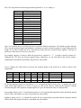
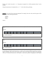
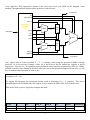
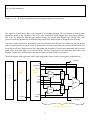
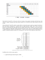
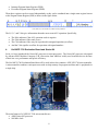
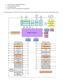
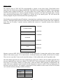
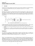
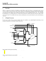
Lesson 02 Introduction to Microcontroller 1. Overview Before we introduce the details of the hardware and software used in this class, it is important to give you an overview of how a processor works. This lesson will provide an information bridge that connects the knowledge you learned from the Digital Logic Design class and what you will be learning from this class. We will begin by introducing a very simple processor. We then briefly discuss the ARM Cortex-M3 processor which will be used in this class. We conclude this lesson with an introduction to the actual hardware used in the laboratory exercises. 2. A Simple Processor To give you an idea of how a processor might work, let’s consider a very simple digital circuit that you can design and implement in the Digital Logic Design class. A_out(3:0) cin opcode(3:0) load_A 0 X(3:0) MUX 4 1 Reg A 4 4 4 sel reset clock ALU 4 Reg B 1 MUX 0 4 4 load_B B_out(3:0) Input signals for this processor include: • clock, reset, sel, load_A, load_B, cin: control signals • X(3:0): 4-bit input data bus • Opcode(3:0): 4-bit control signal that directs what operation the ALU should perform Output signals for this processor include: • A_out(3:0), B_out (3:0): 4-bit output data buses 1 The ALU can perform the following operations (operands: a, b, cin; output: y): Opcode 0000 0001 0010 0011 0100 0101 0110 0111 1000 1001 1010 1011 1100 1101 1110 1111 ALU Operation y = not a y = not b y = a and b y = a or b y = a nand b y = a nor b y = a xor b y = a xnor b y=a y=b y=a+1 y=b+1 y=a–1 y=b–1 y=a+b y = a + b + cin Now, let’s examine how to use this processor to perform different operations. You should recognize that the ALU can only perform logical and arithmetic operations on values stored in register A (regA) and register B (regB). So, in order to utilize the ALU, data must be loaded into one or both of these registers. This type of processor is known as load and store processor. For example, suppose we want to utilize the processor to compute A = 5 – 3 (result is stored in register A). Although the ALU does not directly support binary subtraction, we can still achieve this task by using a combination of operations. Specifically, the processor can perform: A = 5 + complement of 3 + 1. Let us complete the table below to provide the required inputs to the processor in order to achieve this computation. Cycle X sel load_A load_B cin opcode operation Instruction So, for our simple processor, we can achieve A = A – B operation within 4 clock cycles. To produce the correct result, all the input signals (X, sel, load_A, load_B, cin, and opcode) must be inserted at the right time. Instead of memorizing the exact sequence of input signals, let’s give an instruction name to each operation. For example, during cycle 1, 5 is loaded into register A. Let’s represent this operation with an instruction named LDA # (load # into register A) where # represents any 4-bit number. Similarly, during cycle 2, 3 is loaded into register B. Let’s represent this operation with an instruction named LDB # (load # into register B) where # represents any 4-bit number. 2 During cycles 3 and 4, the actual A = A – B operation is computed. Let’s call the operations in these 2 cycles SUBAB. Using the instructions we developed earlier, A = 5 – 3 can be achieved by performing LDA #5 LDB #3 SUBAB Question: Is the order of these instructions important? For example, what is the value stored in register A after the execution of the following instructions? SUBAB LDA #5 LDB #3 Answer: Yes, the order of execution clearly very important. Register A contains a value of 5 after the execution of the instruction sequence above. Example: Complete the table below for an instruction to complement the value in A and store the result back to A. Solution: Cycle X sel load_A load_B cin opcode operation Instruction Let’s call this instruction COMPA. Example: Complete the table below for an instruction to complement the value in B and store the result back to B. Solution: Cycle X sel load_A load_B cin opcode operation Instruction Let’s call this instruction COMPB. It is important to note that the instruction names we came up with to represent different operations are mainly to improve readability. The processor still requires specific values for all input/control signals at the appropriate clock cycle. It means that the processor would require a control unit to generate the appropriate control signals 3 at the right time. This component is known as the instruction decode unit which can be designed a state machine. The updated block diagram for the processor is shown below. A_out(3:0) cin opcode(3:0) load_A Instruction Decode Unit 0 MUX 4 1 X(3:0) 4 Reg A 4 4 instruction sel reset ALU clock 4 Reg B 1 MUX 4 0 load_B negative 4 ALU(3) B_out(3:0) Now, suppose that we want to perform A = |5 – 3| (absolute value) using the operation available with this processor. As in the previous example, values for A and B must first be loaded into registers A and B respectively. Then, the (A – B) operation can be performed with a sequence of instructions (LDA #5, LDB#3, SUBAB) as before. Since finding the absolute value is not one of the operations supported by the ALU, we will have to combine other operations to achieve this. Example: Complete the table below for an instruction to find the absolute value of A and store the result back to register A (A = |A|). To support this operation, the instruction decoder needs to determine if A < 0 (negative). This can be determined based on the MSB of the ALU output. So let’s connect the MSB of the ALU to the decoder. How many clock cycles are required to complete this task? 1st clock cycle complement A and store result in A. 2nd clock cycle either increment A (if sign bit is 0) or complement A (if sign bit is 1), and store result in B. This instruction would require 2 clock cycles to complete. Cycle X sel load_A load_B 4 cin opcode Instruction Let’s call this instruction ABSAN. This is an example of a conditional instruction. The N indicates the negative condition bit of the processor. So now, A = |A – B| can be computed using the following sequence of instructions: LDA #5 LDB #3 SUBAB ABSAN The sequence of instructions above is an example of an assembly program. We can continue to develop more instructions based on the capability of the ALU. More instructions would support more processing capability. This is the key difference with the state machine design you learned from Digital Logic Design class. This processor can be programmed to do different things whereas the state machine is designed to do one thing. You may wonder where these instructions come from and how does the processor make sure that the proper order of instructions are executed? Well, all instructions are stored in an instruction memory (ROM) which can be on-chip or off-chip. Each processor has a functional unit designed to fetch the next instruction to be executed (think of the next state logic in the state machine). The key component of the instruction fetch unit is the Program Counter (PC) which points to the address of the next instruction to be executed. The block diagram of the processor with 3 main components (fetch, decode, execute units) is shown below. A_out(3:0) cin opcode(3:0) load_A Intruction ROM Instruction Fetch Unit Instruction Decode Unit 0 MUX 4 1 X(3:0) 4 Reg A 4 4 sel reset ALU clock 4 Reg B 1 MUX 0 negative load_B negative 4 4 ALU(3) B_out(3:0) Instruction Execution Unit 5 What we have illustrated with this simple processor is the process of fetching, decoding and executing instructions. These 3 steps are mentioned in the book and other technical documents. Now, we have a general idea of how the processor can be designed and utilized to perform a simple program. Next, let’s take a look at the ARM Cortex-M3 processor. 3. Cortex-M3 Processor The general block diagram of Cortex-M3 processor is shown in the figure below. Can you identify the 3 main stages (fetch, decode, execute) of the processor? Fetching stage Decoding stage Execution stage Separate instruction and data memory/busses From The Definitive Guide to ARM Cortex-M3 Processor, Joseph Yiu, Elsevier, 2nd ed, 2009. This processor is designed as a pipelined architecture. Although pipelined architecture is beyond the scope of this course, it is useful to know that pipelined architecture is designed to execute one instruction per cycle. This is possible because pipeline stages operates independently and in parallel (similar to a factory assembly line). The figure below illustrates the optimal performance of a pipelined architecture with 3 main stages: fetch (F), decode (D), and execute (E). As the first instruction (ADD) advances to the decode stage, the next instruction (SUB) is fetched at the same time. Similarly, during the next cycle, as the ADD instruction advances to execute stage, the SUB instruction advances to the decode stage, and a new instruction (ORR) is fetched at the same time. To achieve optimal performance, all stages of the pipelined architecture must be active during a clock cycle. 6 From ARM Cortex-M3 Introduction, ARM University Relations. Note that the Cortex-M3 is a Harvard architecture because it has separate instruction and data busses that connect to separate instruction and data memory modules. We will discuss more about memory in the next section. Note also that the Cortex-M3 contains a register bank (set of general purpose register) to support load and store data from memory (compared to 2 registers from our simple processor earlier). This is also a load-store processor. It means that only load register and store register instructions are allowed to access data from the memory. Registers are high speed storage elements inside the processor. There are 12 general purpose registers, 1 register dedicated to maintain a stack pointer (SP), 1 register is used for return location for subroutines, and 1 register to contain the program counter (PC). All registers are 32-bit wide. These registers are shown below. From Introduction to ARM Cortex-M Microcontroller, Jonathan Valvano, 4nd ed, 2013. In addition, there are three status registers: • Application Program Status Register (APSR) 7 • • Interrupt Program Status Register (IPSR) Execution Program Status Register (EPSR) These three registers can be accessed independently or they can be combined into a single status register known as the Program Status Register (PSR) as shown in the figure below. From ARM Cortex-M3 Introduction, ARM University Relations. The N, Z, C, and V bits give information about the most recent ALU operation. Specifically, • • • • 4. The N bit indicates if the ALU operation result is negative. The Z bit indicates if the result is zero. The C bit indicates if the carry bit is produced in unsigned operation (overflow). And the V bit signifies overflow for operation with signed numbers. Keil MCP 1700 Evaluation Board and Starter Kit So far, we have introduced the Cortex-M3 processor (or microprocessor). The Cortex-M3 processor is designed by Advance RISC Machine Company (U.K.) Processors from ARM are widely used in mobile devices because of their low cost, performance and power efficiency. The Keil MCP 1700 Evaluation Board that will be used in this class contains a NXP LPC1768 microcontroller. A microcontroller combines a microprocessor with on-chip memory for program and data, and i/o peripherals in a single chip. NXP LPC1768 microcontroller The main features of a NXP LPC1768 microcontroller are: • ARM Cortex-M3 processor • 100 MHz clock 8 • • • • 4 32-bit Timer/Counter/PWM units 512 kB instruction ROM 64 kB data RAM Many of I/O and communication peripherals A block diagram of a NXP LPC1768 microcontroller with all supported I/O ports are shown in the figure below From UM10360 LPC17xx User Manual, rev 2, 2010 9 Memory map The memory map of NXP LPC1768 microcontroller is shown in the figure below. Flash ROM where instructions are stored starts at address 0x00000000. Data RAM starts at address 0x10000000. General purpose I/O ports starts at address 0x2009C000. You may wonder why we show GPIO on a memory map. The NXP LPC1768 microcontroller uses memory-mapped technique to interface with input and output ports. It means that each physical input/output pin is mapped to a specific bit in the memory space. We will discuss the memory-mapped I/O ports in more details in the upcoming lessons. Note that the microcontroller maps all hardware components into a continuous memory space (not real, physical memory). Although both the instruction flash memory and data RAM are shown as parts of the same continuous space, they are in reality 2 separate memory modules that connect to 2 separate memory buses (Harvard architecture). 0x00000000 512 KB Flash ROM 0x0007FFFF 0x10000000 64 KB RAM 0x10007FFF 0x2009C000 GPIO 0x2009FFFF Memory system on NXP LPC1768 microcontroller is byte addressable. It means that each byte has a unique address in the memory space. If we want to store a 16-bit into memory, the variable will be stored in 2 bytes. There are two ways these 2 bytes can be stored in memory: 1) little endian order, and 2) big endian order. The little endian approach stores the least significant byte at the lower address. The big endian approach stores the most significant byte at the lower address. The NXP LPC1768 microcontroller uses little endian format. In most cases, if we treat the variable as a single entity, it does not matter which approach is implemented. The order of the bytes (endianess) only becomes relevant when data is stored as words (32 bits) or half-words (16 bits) but is accessed by byte. For example, if an integer (32 bits) variable var has a value of 0x11223344, then var is stored in memory starting at address 0x1000 as: Address 0x1000 0x1001 0x1002 0x1003 Value 10