1
C167 Derivatives
ht
User's Manual 03.96 Version 2.0
tp
:/
Se /ww
m w
ic .s
on ie
du me
ct ns
or .d
/ e/
16-Bit CMOS Single-Chip Microcontrollers
C167
Revision History:
Previous Version:
Page
Page
(in previous (in current
Version)
Version)
Version 2.0 (03.96)
Version 1.0 (08.94)
Preliminary User’s Manual Revision 1.0 (07.92)
Subjects (major changes since last revision)
–
Extension of document scope to C167CR, C167SR, C167S
–
Correction of the items published in the paper "Corrections C167"
Edition 03.96
This edition was realized using the software system FrameMaker.
Published by Siemens AG,
Bereich Halbleiter, MarketingKommunikation, Balanstraße 73,
81541 München
© Siemens AG 1996.
All Rights Reserved.
Attention please!
As far as patents or other rights of third parties are concerned, liability is only assumed for components, not for applications, processes
and circuits implemented within components or assemblies.
The information describes the type of component and shall not be considered as assured characteristics.
Terms of delivery and rights to change design reserved.
For questions on technology, delivery and prices please contact the Semiconductor Group Offices in Germany or the Siemens Companies
and Representatives worldwide (see address list).
Due to technical requirements components may contain dangerous substances. For information on the types in question please contact
your nearest Siemens Office, Semiconductor Group.
Siemens AG is an approved CECC manufacturer.
Packing
Please use the recycling operators known to you. We can also help you – get in touch with your nearest sales office. By agreement we
will take packing material back, if it is sorted. You must bear the costs of transport.
For packing material that is returned to us unsorted or which we are not obliged to accept, we shall have to invoice you for any costs incurred.
Components used in life-support devices or systems must be expressly authorized for such purpose!
Critical components1 of the Semiconductor Group of Siemens AG, may only be used in life-support devices or systems2 with the express
written approval of the Semiconductor Group of Siemens AG.
1 A critical component is a component used in a life-support device or system whose failure can reasonably be expected to cause the
failure of that life-support device or system, or to affect its safety or effectiveness of that device or system.
2 Life support devices or systems are intended (a) to be implanted in the human body, or (b) to support and/or maintain and sustain human life. If they fail, it is reasonable to assume that the health of the user may be endangered.
C167
Table of Contents
Page
1
1.1
1.2
1.3
Introduction . . . . . . . . . . . . . . . . . . . . . . . . . . . . . . . . . . . . . . . . . . . . . . . . 1-1
The Members of the 16-bit Microcontroller Family . . . . . . . . . . . . . . . . . . . . 1-2
Summary of Basic Features . . . . . . . . . . . . . . . . . . . . . . . . . . . . . . . . . . . . . 1-4
Abbreviations . . . . . . . . . . . . . . . . . . . . . . . . . . . . . . . . . . . . . . . . . . . . . . . . 1-7
2
2.1
2.1.1
2.1.2
2.2
2.3
2.4
Architectural Overview . . . . . . . . . . . . . . . . . . . . . . . . . . . . . . . . . . . . . . . 2-1
Basic CPU Concepts and Optimizations . . . . . . . . . . . . . . . . . . . . . . . . . . . 2-2
High Instruction Bandwidth / Fast Execution . . . . . . . . . . . . . . . . . . . . . . . . 2-3
Programmable Multiple Priority Interrupt System . . . . . . . . . . . . . . . . . . . . . 2-6
The On-chip System Resources . . . . . . . . . . . . . . . . . . . . . . . . . . . . . . . . . 2-7
The On-chip Peripheral Blocks . . . . . . . . . . . . . . . . . . . . . . . . . . . . . . . . . 2-11
Protected Bits . . . . . . . . . . . . . . . . . . . . . . . . . . . . . . . . . . . . . . . . . . . . . . . 2-17
3
3.1
3.2
3.3
3.4
3.5
Memory Organization . . . . . . . . . . . . . . . . . . . . . . . . . . . . . . . . . . . . . . . . 3-1
Internal ROM . . . . . . . . . . . . . . . . . . . . . . . . . . . . . . . . . . . . . . . . . . . . . . . . 3-3
Internal RAM and SFR Area . . . . . . . . . . . . . . . . . . . . . . . . . . . . . . . . . . . . 3-4
The On-Chip XRAM . . . . . . . . . . . . . . . . . . . . . . . . . . . . . . . . . . . . . . . . . . . 3-9
External Memory Space . . . . . . . . . . . . . . . . . . . . . . . . . . . . . . . . . . . . . . . 3-11
Crossing Memory Boundaries . . . . . . . . . . . . . . . . . . . . . . . . . . . . . . . . . . 3-12
4
4.1
4.1.1
4.2
4.3
4.4
The Central Processing Unit (CPU) . . . . . . . . . . . . . . . . . . . . . . . . . . . . . 4-1
Instruction Pipelining . . . . . . . . . . . . . . . . . . . . . . . . . . . . . . . . . . . . . . . . . . 4-3
Particular Pipeline Effects . . . . . . . . . . . . . . . . . . . . . . . . . . . . . . . . . . . . . . 4-6
Bit-Handling and Bit-Protection . . . . . . . . . . . . . . . . . . . . . . . . . . . . . . . . . . 4-9
Instruction State Times . . . . . . . . . . . . . . . . . . . . . . . . . . . . . . . . . . . . . . . 4-10
CPU Special Function Registers . . . . . . . . . . . . . . . . . . . . . . . . . . . . . . . . 4-11
5
5.1
5.1.1
5.2
5.3
5.4
5.5
5.5.1
5.6
5.7
Interrupt and Trap Functions . . . . . . . . . . . . . . . . . . . . . . . . . . . . . . . . . . 5-1
Interrupt System Structure . . . . . . . . . . . . . . . . . . . . . . . . . . . . . . . . . . . . . . 5-2
Interrupt Control Registers . . . . . . . . . . . . . . . . . . . . . . . . . . . . . . . . . . . . . . 5-6
Operation of the PEC Channels . . . . . . . . . . . . . . . . . . . . . . . . . . . . . . . . . 5-11
Prioritization of Interrupt and PEC Service Requests . . . . . . . . . . . . . . . . 5-14
Saving the Status during Interrupt Service . . . . . . . . . . . . . . . . . . . . . . . . . 5-15
Interrupt Response Times . . . . . . . . . . . . . . . . . . . . . . . . . . . . . . . . . . . . . 5-17
PEC Response Times . . . . . . . . . . . . . . . . . . . . . . . . . . . . . . . . . . . . . . . . 5-19
External Interrupts . . . . . . . . . . . . . . . . . . . . . . . . . . . . . . . . . . . . . . . . . . . 5-21
Trap Functions . . . . . . . . . . . . . . . . . . . . . . . . . . . . . . . . . . . . . . . . . . . . . . 5-24
6
6.1
6.1.1
6.2
6.2.1
6.3
6.3.1
Parallel Ports . . . . . . . . . . . . . . . . . . . . . . . . . . . . . . . . . . . . . . . . . . . . . . . 6-1
PORT0 . . . . . . . . . . . . . . . . . . . . . . . . . . . . . . . . . . . . . . . . . . . . . . . . . . . . . 6-5
Alternate Functions of PORT0 . . . . . . . . . . . . . . . . . . . . . . . . . . . . . . . . . . . 6-6
PORT1 . . . . . . . . . . . . . . . . . . . . . . . . . . . . . . . . . . . . . . . . . . . . . . . . . . . . . 6-8
Alternate Functions of PORT1 . . . . . . . . . . . . . . . . . . . . . . . . . . . . . . . . . . . 6-9
Port 2 . . . . . . . . . . . . . . . . . . . . . . . . . . . . . . . . . . . . . . . . . . . . . . . . . . . . . 6-11
Alternate Functions of Port 2 . . . . . . . . . . . . . . . . . . . . . . . . . . . . . . . . . . . 6-12
Semiconductor Group
I-1
C167
Table of Contents
Page
6.4
6.4.1
6.5
6.5.1
6.6
6.6.1
6.7
6.7.1
6.8
6.8.1
6.9
6.9.1
Port 3 . . . . . . . . . . . . . . . . . . . . . . . . . . . . . . . . . . . . . . . . . . . . . . . . . . . . . 6-15
Alternate Functions of Port 3 . . . . . . . . . . . . . . . . . . . . . . . . . . . . . . . . . . . 6-16
Port 4 . . . . . . . . . . . . . . . . . . . . . . . . . . . . . . . . . . . . . . . . . . . . . . . . . . . . . 6-20
Alternate Functions of Port 4 . . . . . . . . . . . . . . . . . . . . . . . . . . . . . . . . . . . 6-20
Port 5 . . . . . . . . . . . . . . . . . . . . . . . . . . . . . . . . . . . . . . . . . . . . . . . . . . . . . 6-23
Alternate Functions of Port 5 . . . . . . . . . . . . . . . . . . . . . . . . . . . . . . . . . . . 6-23
Port 6 . . . . . . . . . . . . . . . . . . . . . . . . . . . . . . . . . . . . . . . . . . . . . . . . . . . . . 6-25
Alternate Functions of Port 6 . . . . . . . . . . . . . . . . . . . . . . . . . . . . . . . . . . . 6-26
Port 7 . . . . . . . . . . . . . . . . . . . . . . . . . . . . . . . . . . . . . . . . . . . . . . . . . . . . . 6-30
Alternate Functions of Port 7 . . . . . . . . . . . . . . . . . . . . . . . . . . . . . . . . . . . 6-31
Port 8 . . . . . . . . . . . . . . . . . . . . . . . . . . . . . . . . . . . . . . . . . . . . . . . . . . . . . 6-34
Alternate Functions of Port 8 . . . . . . . . . . . . . . . . . . . . . . . . . . . . . . . . . . . 6-35
7
Dedicated Pins . . . . . . . . . . . . . . . . . . . . . . . . . . . . . . . . . . . . . . . . . . . . . . 7-1
8
8.1
8.2
8.3
8.4
8.5
8.6
8.7
The External Bus Interface . . . . . . . . . . . . . . . . . . . . . . . . . . . . . . . . . . . . 8-1
External Bus Modes . . . . . . . . . . . . . . . . . . . . . . . . . . . . . . . . . . . . . . . . . . . 8-2
Programmable Bus Characteristics . . . . . . . . . . . . . . . . . . . . . . . . . . . . . . 8-10
READY Controlled Bus Cycles . . . . . . . . . . . . . . . . . . . . . . . . . . . . . . . . . 8-15
Controlling the External Bus Controller . . . . . . . . . . . . . . . . . . . . . . . . . . . 8-16
EBC Idle State . . . . . . . . . . . . . . . . . . . . . . . . . . . . . . . . . . . . . . . . . . . . . . 8-24
External Bus Arbitration . . . . . . . . . . . . . . . . . . . . . . . . . . . . . . . . . . . . . . . 8-25
The XBUS Interface . . . . . . . . . . . . . . . . . . . . . . . . . . . . . . . . . . . . . . . . . . 8-29
9
9.1
9.1.1
9.1.2
9.1.3
9.2
9.2.1
9.2.2
9.2.3
The General Purpose Timer Units . . . . . . . . . . . . . . . . . . . . . . . . . . . . . . 9-1
Timer Block GPT1 . . . . . . . . . . . . . . . . . . . . . . . . . . . . . . . . . . . . . . . . . . . . 9-1
GPT1 Core Timer T3 . . . . . . . . . . . . . . . . . . . . . . . . . . . . . . . . . . . . . . . . . . 9-3
GPT1 Auxiliary Timers T2 and T4 . . . . . . . . . . . . . . . . . . . . . . . . . . . . . . . . 9-8
Interrupt Control for GPT1 Timers . . . . . . . . . . . . . . . . . . . . . . . . . . . . . . . 9-15
Timer Block GPT2 . . . . . . . . . . . . . . . . . . . . . . . . . . . . . . . . . . . . . . . . . . . 9-16
GPT2 Core Timer T6 . . . . . . . . . . . . . . . . . . . . . . . . . . . . . . . . . . . . . . . . . 9-18
GPT2 Auxiliary Timer T5 . . . . . . . . . . . . . . . . . . . . . . . . . . . . . . . . . . . . . . 9-23
Interrupt Control for GPT2 Timers and CAPREL . . . . . . . . . . . . . . . . . . . . 9-31
10
10.1
10.2
10.3
10.4
10.5
The Asynchronous/Synchronous Serial Interface . . . . . . . . . . . . . . . . 10-1
Asynchronous Operation . . . . . . . . . . . . . . . . . . . . . . . . . . . . . . . . . . . . . . 10-4
Synchronous Operation . . . . . . . . . . . . . . . . . . . . . . . . . . . . . . . . . . . . . . . 10-8
Hardware Error Detection Capabilities . . . . . . . . . . . . . . . . . . . . . . . . . . . 10-10
ASC0 Baud Rate Generation . . . . . . . . . . . . . . . . . . . . . . . . . . . . . . . . . . 10-10
ASC0 Interrupt Control . . . . . . . . . . . . . . . . . . . . . . . . . . . . . . . . . . . . . . . 10-12
11
11.1
11.2
11.3
The High-Speed Synchronous Serial Interface . . . . . . . . . . . . . . . . . . . 11-1
Full-Duplex Operation . . . . . . . . . . . . . . . . . . . . . . . . . . . . . . . . . . . . . . . . 11-6
Half Duplex Operation . . . . . . . . . . . . . . . . . . . . . . . . . . . . . . . . . . . . . . . . 11-8
Baud Rate Generation . . . . . . . . . . . . . . . . . . . . . . . . . . . . . . . . . . . . . . . 11-10
Semiconductor Group
I-2
C167
Table of Contents
11.4
11.5
Page
Error Detection Mechanisms . . . . . . . . . . . . . . . . . . . . . . . . . . . . . . . . . . 11-12
SSC Interrupt Control . . . . . . . . . . . . . . . . . . . . . . . . . . . . . . . . . . . . . . . . 11-14
12
The Watchdog Timer (WDT) . . . . . . . . . . . . . . . . . . . . . . . . . . . . . . . . . . 12-1
12.0.1 Operation of the Watchdog Timer . . . . . . . . . . . . . . . . . . . . . . . . . . . . . . . 12-2
13
The Bootstrap Loader . . . . . . . . . . . . . . . . . . . . . . . . . . . . . . . . . . . . . . . 13-1
14
14.1
14.2
14.3
14.3.1
14.4
14.5
14.5.1
14.6
The Capture / Compare Units . . . . . . . . . . . . . . . . . . . . . . . . . . . . . . . . . 14-1
The CAPCOM Timers . . . . . . . . . . . . . . . . . . . . . . . . . . . . . . . . . . . . . . . . 14-4
CAPCOM Unit Timer Interrupts . . . . . . . . . . . . . . . . . . . . . . . . . . . . . . . . . 14-8
Capture/Compare Registers . . . . . . . . . . . . . . . . . . . . . . . . . . . . . . . . . . . 14-9
Selection of Capture Modes and Compare Modes . . . . . . . . . . . . . . . . . 14-11
Capture Mode . . . . . . . . . . . . . . . . . . . . . . . . . . . . . . . . . . . . . . . . . . . . . 14-12
Compare Modes, . . . . . . . . . . . . . . . . . . . . . . . . . . . . . . . . . . . . . . . . . . . 14-13
Double-Register Compare Mode . . . . . . . . . . . . . . . . . . . . . . . . . . . . . . . 14-18
Capture/Compare Interrupts . . . . . . . . . . . . . . . . . . . . . . . . . . . . . . . . . . 14-20
15
15.1
15.2
15.3
15.4
The Pulse Width Modulation Module . . . . . . . . . . . . . . . . . . . . . . . . . . . 15-1
Operating Modes . . . . . . . . . . . . . . . . . . . . . . . . . . . . . . . . . . . . . . . . . . . . 15-2
PWM Module Registers . . . . . . . . . . . . . . . . . . . . . . . . . . . . . . . . . . . . . . . 15-7
Interrupt Request Generation . . . . . . . . . . . . . . . . . . . . . . . . . . . . . . . . . . 15-11
PWM Output Signals . . . . . . . . . . . . . . . . . . . . . . . . . . . . . . . . . . . . . . . . 15-12
16
16.1
16.2
16.3
The Analog / Digital Converter . . . . . . . . . . . . . . . . . . . . . . . . . . . . . . . . 16-1
Mode Selection and Operation . . . . . . . . . . . . . . . . . . . . . . . . . . . . . . . . . . 16-3
Conversion Timing Control . . . . . . . . . . . . . . . . . . . . . . . . . . . . . . . . . . . . 16-10
A/D Converter Interrupt Control . . . . . . . . . . . . . . . . . . . . . . . . . . . . . . . . 16-11
17
System Reset . . . . . . . . . . . . . . . . . . . . . . . . . . . . . . . . . . . . . . . . . . . . . . 17-1
17.0.1 System Startup Configuration . . . . . . . . . . . . . . . . . . . . . . . . . . . . . . . . . . 17-7
18
18.1
18.2
18.3
Power Reduction Modes . . . . . . . . . . . . . . . . . . . . . . . . . . . . . . . . . . . . . 18-1
Idle Mode . . . . . . . . . . . . . . . . . . . . . . . . . . . . . . . . . . . . . . . . . . . . . . . . . . 18-1
Power Down Mode . . . . . . . . . . . . . . . . . . . . . . . . . . . . . . . . . . . . . . . . . . . 18-3
Status of Output Pins during Idle and Power Down Mode . . . . . . . . . . . . . 18-4
19
19.1
19.2
19.3
19.4
19.5
19.6
19.7
19.8
System Programming . . . . . . . . . . . . . . . . . . . . . . . . . . . . . . . . . . . . . . . 19-1
Stack Operations . . . . . . . . . . . . . . . . . . . . . . . . . . . . . . . . . . . . . . . . . . . . 19-4
Register Banking . . . . . . . . . . . . . . . . . . . . . . . . . . . . . . . . . . . . . . . . . . . . 19-8
Procedure Call Entry and Exit . . . . . . . . . . . . . . . . . . . . . . . . . . . . . . . . . . 19-8
Table Searching . . . . . . . . . . . . . . . . . . . . . . . . . . . . . . . . . . . . . . . . . . . . 19-11
Peripheral Control and Interface . . . . . . . . . . . . . . . . . . . . . . . . . . . . . . . 19-11
Floating Point Support . . . . . . . . . . . . . . . . . . . . . . . . . . . . . . . . . . . . . . . 19-12
Trap/Interrupt Entry and Exit . . . . . . . . . . . . . . . . . . . . . . . . . . . . . . . . . . 19-12
Unseparable Instruction Sequences . . . . . . . . . . . . . . . . . . . . . . . . . . . . 19-12
Semiconductor Group
I-3
C167
Table of Contents
Page
19.9
19.10
19.11
Overriding the DPP Addressing Mechanism . . . . . . . . . . . . . . . . . . . . . . 19-13
Handling the Internal ROM . . . . . . . . . . . . . . . . . . . . . . . . . . . . . . . . . . . . 19-14
Pits, Traps and Mines . . . . . . . . . . . . . . . . . . . . . . . . . . . . . . . . . . . . . . . 19-15
20
20.0.1
20.1
20.2
20.3
20.4
The Register Set . . . . . . . . . . . . . . . . . . . . . . . . . . . . . . . . . . . . . . . . . . . . 20-1
Register Description Format . . . . . . . . . . . . . . . . . . . . . . . . . . . . . . . . . . . 20-1
CPU General Purpose Registers (GPRs) . . . . . . . . . . . . . . . . . . . . . . . . . 20-2
Special Function Registers ordered by Name . . . . . . . . . . . . . . . . . . . . . . 20-4
Registers ordered by Address . . . . . . . . . . . . . . . . . . . . . . . . . . . . . . . . . 20-12
Special Notes . . . . . . . . . . . . . . . . . . . . . . . . . . . . . . . . . . . . . . . . . . . . . . 20-19
21
Instruction Set Summary . . . . . . . . . . . . . . . . . . . . . . . . . . . . . . . . . . . . . 21-1
22
Device Specification . . . . . . . . . . . . . . . . . . . . . . . . . . . . . . . . . . . . . . . . 22-1
23
The On-Chip CAN Interface . . . . . . . . . . . . . . . . . . . . . . . . . . . . . . . . . . . 23-1
24
Keyword Index . . . . . . . . . . . . . . . . . . . . . . . . . . . . . . . . . . . . . . . . . . . . . 24-1
Semiconductor Group
I-4
Introduction / C167
1
Introduction
The rapidly growing area of embedded control applications is representing one of the most timecritical operating environments for today’s microcontrollers. Complex control algorithms have to be
processed based on a large number of digital as well as analog input signals, and the appropriate
output signals must be generated within a defined maximum response time. Embedded control
applications also are often sensitive to board space, power consumption, and overall system cost.
Embedded control applications therefore require microcontrollers, which...
• offer a high level of system integration
• eliminate the need for additional peripheral devices and the associated software overhead
• provide system security and fail-safe mechanisms.
With the increasing complexity of embedded control applications, a significant increase in CPU
performance and peripheral functionality over conventional 8-bit controllers is required from
microcontrollers for high-end embedded control systems. In order to achieve this high performance
goal Siemens has decided to develop its family of 16-bit CMOS microcontrollers without the
constraints of backward compatibility.
Of course the architecture of the 16-bit microcontroller family pursues successfull hardware and
software concepts, which have been established in Siemens's popular 8-bit controller families.
About this Manual
This manual describes the functionality of a number of 16-bit microcontrollers of the Siemens C166family, the socalled C167-class.
As these microcontrollers provide a great extent of identical functionality it makes sense to describe
a superset of the provided features. For this reason some sections of this manual do not refer to all
the C167 derivatives that are offered (eg. devices without a CAN interface). These sections contain
respective notes wherever possible.
The descriptions in this manual refer to the following derivatives of the C167-class:
●
●
●
●
●
●
●
C167CR-LM
C167CR-4RM
C167CR-16RM
C167CR-16FM
C167SR-LM
C167S-4RM
C167-LM
Version with PLL, 2 KByte XRAM, CAN module
Version with PLL, 2 KByte XRAM, 32 KByte ROM, CAN module
Version with PLL, 2 KByte XRAM, 128 KByte ROM, CAN module
Version with PLL, 2 KByte XRAM, 128 KByte Flash memory, CAN module
Version with PLL, 2 KByte XRAM
Version with PLL, 32 KByte ROM
Basic version
This manual is valid for the versions with on-chip ROM or Flash memory of the mentioned
derivatives as well as for the romless versions. Of course it refers to all devices of the different
available temperature ranges and packages.
For simplicity all these various versions are referred to by the term C167 throughout this manual.
The complete pro-electron comform designations are listed in the respective data sheets.
Semiconductor Group
1-1
Introduction / C167
1.1
The Members of the 16-bit Microcontroller Family
The microcontrollers of the Siemens 16-bit family have been designed to meet the high
performance requirements of real-time embedded control applications. The architecture of this
family has been optimized for high instruction throughput and minimum response time to external
stimuli (interrupts). Intelligent peripheral subsystems have been integrated to reduce the need for
CPU intervention to a minimum extent. This also minimizes the need for communication via the
external bus interface. The high flexibility of this architecture allows to serve the diverse and varying
needs of different application areas such as automotive, industrial control, or data communications.
The core of the 16-bit family has been developped with a modular family concept in mind. All family
members execute an efficient control-optimized instruction set (additional instructions for members
of the second generation). This allows an easy and quick implementation of new family members
with different internal memory sizes and technologies, different sets of on-chip peripherals and/or
different numbers of IO pins.
The XBUS concept opens a straight forward path for the integration of application specific
peripheral modules in addition to the standard on-chip peripherals in order to build application
specific derivatives.
As programs for embedded control applications become larger, high level languages are favoured
by programmers, because high level language programs are easier to write, to debug and to
maintain.
Semiconductor Group
1-2
Introduction / C167
The 80C166-type microcontrollers were the first generation of the 16-bit controller family. These
devices have established the C16x architecture.
The C165-type and C167-type devices are members of the second generation of this family. This
second generation is even more powerful due to additional instructions for HLL support, an
increased address space, increased internal RAM and highly efficient management of various
resources on the external bus.
Enhanced derivatives of this second generation provide additional features like additional internal
high-speed RAM, an integrated CAN-Module, an on-chip PLL, etc.
Utilizing integration to design efficient systems may require the integration of application specific
peripherals to boost system performance, while minimizing the part count. These efforts are
supported by the so-called XBUS, defined for the Siemens 16-bit microcontrollers (second
generation). This XBUS is an internal representation of the external bus interface that opens and
simplifies the integration of peripherals by standardizing the required interface. One representative
taking advantage of this technology is the integrated CAN module that is offered by some devices.
The C165-type devices are reduced versions of the C167 which provide a smaller package and
reduced power consumption at the expense of the A/D converter, the CAPCOM units and the PWM
module.
A variety of different versions is provided which offer mask-programmable ROM, Flash memory or
no non-volatile memory at all. Also there are devices with specific functional units.
The devices may be offered in different packages, temperature ranges and speed classes.
More standard and application-specific derivatives are planned and in development.
Information about specific versions and derivatives will be made available with the devices
themselves. Contact your Siemens representative for up-to-date material.
Note: As the architecture and the basic features (ie. CPU core and built in peripherals) are identical
for most of the currently offered versions of the C167, the descriptions within this manual that
refer to the “C167” also apply to the other variations, unless otherwise noted.
Semiconductor Group
1-3
Introduction / C167
1.2
Summary of Basic Features
The C167 is an improved representative of the Siemens family of full featured 16-bit single-chip
CMOS microcontrollers. It combines high CPU performance (up to 10 million instructions per
second) with high peripheral functionality.
Several key features contribute to the high performance of the C167 (the indicated timings refer to
a CPU clock of 20 MHz).
High Performance 16-Bit CPU With Four-Stage Pipeline
•
•
•
•
•
•
•
100 ns minimum instruction cycle time, with most instructions executed in 1 cycle
500 ns multiplication (16-bit *16-bit), 1 µs division (32-bit/16-bit)
Multiple high bandwidth internal data buses
Register based design with multiple variable register banks
Single cycle context switching support
16 MBytes linear address space for code and data (von Neumann architecture)
System stack cache support with automatic stack overflow/underflow detection
Control Oriented Instruction Set with High Efficiency
•
•
•
•
•
Bit, byte, and word data types
Flexible and efficient addressing modes for high code density
Enhanced boolean bit manipulation with direct addressability of 6 Kbits
for peripheral control and user defined flags
Hardware traps to identify exception conditions during runtime
HLL support for semaphore operations and efficient data access
Integrated On-chip Memory
•
•
•
2 KByte internal RAM for variables, register banks, system stack and code
2 KByte on-chip high-speed XRAM for variables, user stack and code (not on all derivatives)
Internal Mask ROM or Flash memory (not for romless devices)
External Bus Interface
•
•
•
•
Multiplexed or demultiplexed bus configurations
Segmentation capability and chip select signal generation
8-bit or 16-bit data bus
Bus cycle characteristics selectable for five programmable address areas
16-Priority-Level Interrupt System
•
•
•
56 interrupt nodes with separate interrupt vectors
300/500 ns typical/maximum interrupt latency in case of internal program execution
Fast external interrupts
Semiconductor Group
1-4
Introduction / C167
8-Channel Peripheral Event Controller (PEC)
•
•
•
Interrupt driven single cycle data transfer
Transfer count option (standard CPU interrupt after a programmable
number of PEC transfers)
Eliminates overhead of saving and restoring system state for interrupt requests
Intelligent On-chip Peripheral Subsystems
•
•
•
•
•
•
•
•
•
16-Channel 10-bit A/D Converter with programmable conversion time
(9.7 µs minimum), auto scan modes, channel injection mode
Two 16-Channel Capture/Compare Units with 2 independent time bases each,
very flexible PWM unit/event recording unit with 5 different operating modes,
includes four 16-bit timers/counters with 400 ns maximum resolution
4-Channel PWM Unit
2 Multifunctional General Purpose Timer Units
GPT1: three 16-bit timers/ counters, 400 ns maximum resolution
GPT2: two 16-bit timers/counters, 200 ns maximum resolution
Asynchronous/Synchronous Serial Channel (USART)
with baud rate generator, parity, framing, and overrun error detection
High Speed Synchronous Serial Channel
programmable data length and shift direction
Watchdog Timer with programmable time intervals
Bootstrap Loader for flexible system initialization
On-chip CAN-Module (not on all derivatives)
111 IO Lines With Individual Bit Addressability
•
•
•
Tri-stated in input mode
Push/pull or open drain output mode
Selectable input thresholds (not on all derivatives)
Different Temperature Ranges
•
0 to +70 °C, – 40 to +85 °C, – 40 to +110 °C
Siemens CMOS Process
•
Low Power CMOS Technology, including power saving Idle and Power Down modes
144-Pin Plastic Quad Flat Pack (PQFP) Package
•
EIAJ standard, 0.65 mm (25.6 mil) lead spacing, surface mount technology
Semiconductor Group
1-5
Introduction / C167
Complete Development Support
A variety of software and hardware development tools for the Siemens family of 16-bit
microcontrollers is available from experienced international tool suppliers. The high quality and
reliability of these tools is already proven in many applications and by many users. The tool
environment for the Siemens 16-bit microcontrollers includes the following tools:
•
•
•
•
•
•
•
•
•
•
•
•
•
Compilers (C, MODULA2, FORTH)
Macro-Assemblers, Linkers, Locaters, Library Managers, Format-Converters
Architectural Simulators
HLL debuggers
Real-Time operating systems
VHDL chip models
In-Circuit Emulators (based on bondout or standard chips)
Plug-In emulators
Emulation and Clip-Over adapters, production sockets
Logic Analyzer disassemblers
Evaluation Boards with monitor programs
Industrial boards (also for CAN, FUZZY, PROFIBUS, FORTH applications)
Network driver software (CAN, PROFIBUS)
Semiconductor Group
1-6
Introduction / C167
1.3
Abbreviations
The following acronyms and termini are used within this document:
ADC . . . . . . . . . Analog Digital Converter
ALE . . . . . . . . . . Address Latch Enable
ALU . . . . . . . . . . Arithmetic and Logic Unit
ASC. . . . . . . . . . Asynchronous/synchronous Serial Controller
CAN . . . . . . . . . Controller Area Network (License Bosch)
CAPCOM . . . . . CAPture and COMpare unit
CISC . . . . . . . . . Complex Instruction Set Computing
CMOS . . . . . . . . Complementary Metal Oxide Silicon
CPU . . . . . . . . . Central Processing Unit
EBC. . . . . . . . . . External Bus Controller
ESFR . . . . . . . . Extended Special Function Register
Flash . . . . . . . . . Non-volatile memory that may be electrically erased
GPR . . . . . . . . . General Purpose Register
GPT. . . . . . . . . . General Purpose Timer unit
HLL . . . . . . . . . . High Level Language
IO . . . . . . . . . . . Input / Output
PEC. . . . . . . . . . Peripheral Event Controller
PLA . . . . . . . . . . Programmable Logic Array
PLL . . . . . . . . . . Phase Locked Loop
PWM . . . . . . . . . Pulse Width Modulation
RAM . . . . . . . . . Random Access Memory
RISC . . . . . . . . . Reduced Instruction Set Computing
ROM . . . . . . . . . Read Only Memory
SFR. . . . . . . . . . Special Function Register
SSC. . . . . . . . . . Synchronous Serial Controller
XBUS . . . . . . . . Internal representation of the External Bus
XRAM . . . . . . . . On-chip extension RAM
Semiconductor Group
1-7
Architectural Overview / C167
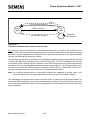
2
Architectural Overview
The architecture of the C167 combines the advantages of both RISC and CISC processors in a very
well-balanced way. The sum of the features which are combined result in a high performance
microcontroller, which is the right choice not only for today’s applications, but also for future
engineering challenges. The C167 not only integrates a powerful CPU core and a set of peripheral
units into one chip, but also connects the units in a very efficient way. One of the four buses used
concurrently on the C167 is the XBUS, an internal representation of the external bus interface. This
bus provides a standardized method of integrating application-specific peripherals to produce
derivates of the standard C167.
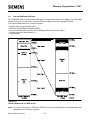
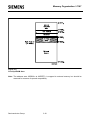
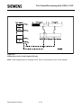
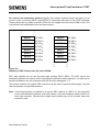
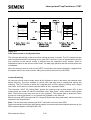
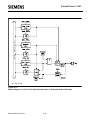
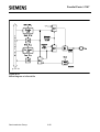
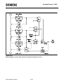
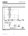
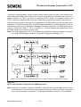
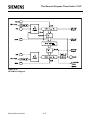
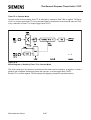
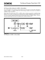
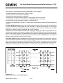
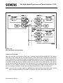
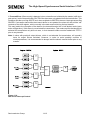
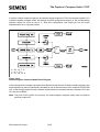
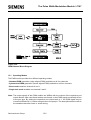
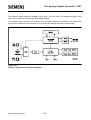
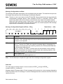
Figure 2-1
C167 Functional Block Diagram
Semiconductor Group
2-1
Architectural Overview / C167
2.1
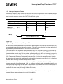
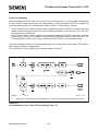
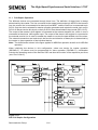
Basic CPU Concepts and Optimizations
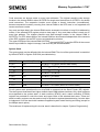
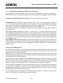
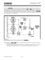
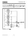
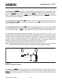
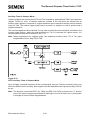
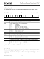
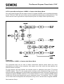
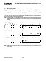
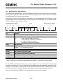
The main core of the CPU consists of a 4-stage instruction pipeline, a 16-bit arithmetic and logic unit
(ALU) and dedicated SFRs. Additional hardware is provided for a separate multiply and divide unit,
a bit-mask generator and a barrel shifter.
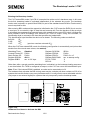
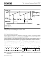
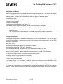
Figure 2-2
CPU Block Diagram
To meet the demand for greater performance and flexibility, a number of areas has been optimized
in the processor core. Functional blocks in the CPU core are controlled by signals from the
instruction decode logic. These are summarized below, and described in detail in the following
sections:
1) High Instruction Bandwidth / Fast Execution
2) High Function 8-bit and 16-bit Arithmetic and Logic Unit
3) Extended Bit Processing and Peripheral Control
4) High Performance Branch-, Call-, and Loop Processing
5) Consistent and Optimized Instruction Formats
6) Programmable Multiple Priority Interrupt Structure
Semiconductor Group
2-2
Architectural Overview / C167
High Instruction Bandwidth / Fast Execution
Based on the hardware provisions, most of the C167’s instructions can be executed in just one
machine cycle, which requires 100 ns at 20 MHz CPU clock. For example, shift and rotate
instructions are always processed within one machine cycle, independent of the number of bits to
be shifted.
Branch-, multiply- and divide instructions normally take more than one machine cycle. These
instructions, however, have also been optimized. For example, branch instructions only require an
additional machine cycle, when a branch is taken, and most branches taken in loops require no
additional machine cycles at all, due to the so-called ‘Jump Cache’.
A 32-bit / 16-bit division takes 1µs, a 16-bit * 16-bit multiplication takes 0.5 µs.
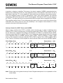
The instruction cycle time has been dramatically reduced through the use of instruction pipelining.
This technique allows the core CPU to process portions of multiple sequential instruction stages in
parallel. The following four stage pipeline provides the optimum balancing for the CPU core:
FETCH: In this stage, an instruction is fetched from the internal ROM or RAM or from the external
memory, based on the current IP value.
DECODE: In this stage, the previously fetched instruction is decoded and the required operands
are fetched.
EXECUTE: In this stage, the specified operation is performed on the previously fetched operands.
WRITE BACK: In this stage, the result is written to the specified location.
If this technique were not used, each instruction would require four machine cycles. This increased
performance allows a greater number of tasks and interrupts to be processed.
Instruction Decoder
Instruction decoding is primarily generated from PLA outputs based on the selected opcode. No
microcode is used and each pipeline stage receives control signals staged in control registers from
the decode stage PLAs. Pipeline holds are primarily caused by wait states for external memory
accesses and cause the holding of signals in the control registers. Multiple-cycle instructions are
performed through instruction injection and simple internal state machines which modify required
control signals.
High Function 8-bit and 16-bit Arithmetic and Logic Unit
All standard arithmetic and logical operations are performed in a 16-bit ALU. In addition, for byte
operations, signals are provided from bits six and seven of the ALU result to correctly set the
condition flags. Multiple precision arithmetic is provided through a 'CARRY-IN' signal to the ALU
from previously calculated portions of the desired operation. Most internal execution blocks have
been optimized to perform operations on either 8-bit or 16-bit quantities. Once the pipeline has been
filled, one instruction is completed per machine cycle, except for multiply and divide. An advanced
Booth algorithm has been incorporated to allow four bits to be multiplied and two bits to be divided
per machine cycle. Thus, these operations use two coupled 16-bit registers, MDL and MDH, and
require four and nine machine cycles, respectively, to perform a 16-bit by 16-bit (or 32-bit by 16-bit)
calculation plus one machine cycle to setup and adjust the operands and the result. Even these
Semiconductor Group
2-3
Architectural Overview / C167
longer multiply and divide instructions can be interrupted during their execution to allow for very fast
interrupt response. Instructions have also been provided to allow byte packing in memory while
providing sign extension of bytes for word wide arithmetic operations. The internal bus structure
also allows transfers of bytes or words to or from peripherals based on the peripheral requirements.
A set of consistent flags is automatically updated in the PSW after each arithmetic, logical, shift, or
movement operation. These flags allow branching on specific conditions. Support for both signed
and unsigned arithmetic is provided through user-specifiable branch tests. These flags are also
preserved automatically by the CPU upon entry into an interrupt or trap routine.
All targets for branch calculations are also computed in the central ALU.
A 16-bit barrel shifter provides multiple bit shifts in a single cycle. Rotates and arithmetic shifts are
also supported.
Extended Bit Processing and Peripheral Control
A large number of instructions has been dedicated to bit processing. These instructions provide
efficient control and testing of peripherals while enhancing data manipulation. Unlike other
microcontrollers, these instructions provide direct access to two operands in the bit-addressable
space without requiring to move them into temporary flags.
The same logical instructions available for words and bytes are also supported for bits. This allows
the user to compare and modify a control bit for a peripheral in one instruction. Multiple bit shift
instructions have been included to avoid long instruction streams of single bit shift operations.
These are also performed in a single machine cycle.
In addition, bit field instructions have been provided, which allow the modification of multiple bits
from one operand in a single instruction.
High Performance Branch-, Call-, and Loop Processing
Due to the high percentage of branching in controller applications, branch instructions have been
optimized to require one extra machine cycle only when a branch is taken. This is implemented by
precalculating the target address while decoding the instruction. To decrease loop execution
overhead, three enhancements have been provided:
• The first solution provides single cycle branch execution after the first iteration of a loop. Thus, only
one machine cycle is lost during the execution of the entire loop. In loops which fall through upon
completion, no machine cycles are lost when exiting the loop. No special instructions are required
to perform loops, and loops are automatically detected during execution of branch instructions.
• The second loop enhancement allows the detection of the end of a table and avoids the use of two
compare instructions embedded in loops. One simply places the lowest negative number at the end
of the specific table, and specifies branching if neither this value nor the compared value have been
found. Otherwise the loop is terminated if either condition has been met. The terminating condition
can then be tested.
• The third loop enhancement provides a more flexible solution than the Decrement and Skip on
Zero instruction which is found in other microcontrollers. Through the use of Compare and
Increment or Decrement instructions, the user can make comparisons to any value. This allows loop
counters to cover any range. This is particularly advantageous in table searching.
Semiconductor Group
2-4
Architectural Overview / C167
Saving of system state is automatically performed on the internal system stack avoiding the use of
instructions to preserve state upon entry and exit of interrupt or trap routines. Call instructions push
the value of the IP on the system stack, and require the same execution time as branch instructions.
Instructions have also been provided to support indirect branch and call instructions. This supports
implementation of multiple CASE statement branching in assembler macros and high level
languages.
Consistent and Optimized Instruction Formats
To obtain optimum performance in a pipelined design, an instruction set has been designed which
incorporates concepts from Reduced Instruction Set Computing (RISC). These concepts primarily
allow fast decoding of the instructions and operands while reducing pipeline holds. These concepts,
however, do not preclude the use of complex instructions, which are required by microcontroller
users. The following goals were used to design the instruction set:
1)
2)
3)
Provide powerful instructions to perform operations which currently require sequences of
instructions and are frequently used. Avoid transfer into and out of temporary registers such
as accumulators and carry bits. Perform tasks in parallel such as saving state upon entry into
interrupt routines or subroutines.
Avoid complex encoding schemes by placing operands in consistent fields for each instruction. Also avoid complex addressing modes which are not frequently used. This decreases
the instruction decode time while also simplifying the development of compilers and assemblers.
Provide most frequently used instructions with one-word instruction formats. All other instructions are placed into two-word formats. This allows all instructions to be placed on word
boundaries, which alleviates the need for complex alignment hardware. It also has the benefit of increasing the range for relative branching instructions.
The high performance offered by the hardware implementation of the CPU can efficiently be utilized
by a programmer via the highly functional C167 instruction set which includes the following
instruction classes:
•
•
•
•
•
•
•
•
•
•
•
•
Arithmetic Instructions
Logical Instructions
Boolean Bit Manipulation Instructions
Compare and Loop Control Instructions
Shift and Rotate Instructions
Prioritize Instruction
Data Movement Instructions
System Stack Instructions
Jump and Call Instructions
Return Instructions
System Control Instructions
Miscellaneous Instructions
Possible operand types are bits, bytes and words. Specific instruction support the conversion
(extension) of bytes to words. A variety of direct, indirect or immediate addressing modes are
provided to specify the required operands.
Semiconductor Group
2-5
Architectural Overview / C167
Programmable Multiple Priority Interrupt System
The following enhancements have been included to allow processing of a large number of interrupt
sources:
1)
Peripheral Event Controller (PEC): This processor is used to off-load many interrupt requests
from the CPU. It avoids the overhead of entering and exiting interrupt or trap routines by performing single-cycle interrupt-driven byte or word data transfers between any two locations in
segment 0 with an optional increment of either the PEC source or the destination pointer.
Just one cycle is ’stolen’ from the current CPU activity to perform a PEC service.
2)
Multiple Priority Interrupt Controller: This controller allows all interrupts to be placed at any
specified priority. Interrupts may also be grouped, which provides the user with the ability to
prevent similar priority tasks from interrupting each other. For each of the possible interrupt
sources there is a separate control register, which contains an interrupt request flag, an interrupt enable flag and an interrupt priority bitfield. Once having been accepted by the CPU, an
interrupt service can only be interrupted by a higher prioritized service request. For standard
interrupt processing, each of the possible interrupt sources has a dedicated vector location.
3)
Multiple Register Banks: This feature allows the user to specify up to sixteen general purpose registers located anywhere in the internal RAM. A single one-machine-cycle instruction
allows to switch register banks from one task to another.
4)
Interruptable Multiple Cycle Instructions: Reduced interrupt latency is provided by allowing
multiple-cycle instructions (multiply, divide) to be interruptable.
With an interrupt response time within a range from just 250 ns to 500 ns (in case of internal
program execution), the C167 is capable of reacting very fast on non-deterministic events.
Its fast external interrupt inputs are sampled every 50 ns and allow to recognize even very short
external signals.
The C167 also provides an excellent mechanism to identify and to process exceptions or error
conditions that arise during run-time, so called ’Hardware Traps’. Hardware traps cause an
immediate non-maskable system reaction which is similiar to a standard interrupt service
(branching to a dedicated vector table location). The occurrence of a hardware trap is additionally
signified by an individual bit in the trap flag register (TFR). Except for another higher prioritized trap
service being in progress, a hardware trap will interrupt any current program execution. In turn,
hardware trap services can normally not be interrupted by standard or PEC interrupts.
Software interrupts are supported by means of the ’TRAP’ instruction in combination with an
individual trap (interrupt) number.
Semiconductor Group
2-6
Architectural Overview / C167
2.2
The On-chip System Resources
The C167 controllers provide a number of powerful system resources designed around the CPU.
The combination of CPU and these resources results in the high performance of the members of
this controller family.
Peripheral Event Controller (PEC) and Interrupt Control
The Peripheral Event Controller allows to respond to an interrupt request with a single data transfer
(word or byte) which only consumes one instruction cycle and does not require to save and restore
the machine status. Each interrupt source is prioritized every machine cycle in the interrupt control
block. If PEC service is selected, a PEC transfer is started. If CPU interrupt service is requested, the
current CPU priority level stored in the PSW register is tested to determine whether a higher priority
interrupt is currently being serviced. When an interrupt is acknowledged, the current state of the
machine is saved on the internal system stack and the CPU branches to the system specific vector
for the peripheral.
The PEC contains a set of SFRs which store the count value and control bits for eight data transfer
channels. In addition, the PEC uses a dedicated area of RAM which contains the source and
destination addresses. The PEC is controlled similar to any other peripheral through SFRs
containing the desired configuration of each channel.
An individual PEC transfer counter is implicitly decremented for each PEC service except forming
in the continuous transfer mode. When this counter reaches zero, a standard interrupt is performed
to the vector location related to the corresponding source. PEC services are very well suited, for
example, to move register contents to/from a memory table. The C167 has 8 PEC channels each
of which offers such fast interrupt-driven data transfer capabilities.
Memory Areas
The memory space of the C167 is configured in a Von Neumann architecture which means that
code memory, data memory, registers and IO ports are organized within the same linear address
space which covers up to 16 MBytes. The entire memory space can be accessed bytewise or
wordwise. Particular portions of the on-chip memory have additionally been made directly bit
addressable.
A 2 KByte 16-bit wide internal RAM provides fast access to General Purpose Registers (GPRs),
user data (variables) and system stack. The internal RAM may also be used for code. A unique
decoding scheme provides flexible user register banks in the internal memory while optimizing the
remaining RAM for user data.
The CPU disposes of an actual register context consisting of up to 16 wordwide and/or bytewide
GPRs, which are physically located within the on-chip RAM area. A Context Pointer (CP) register
determines the base address of the active register bank to be accessed by the CPU at a time. The
number of register banks is only restricted by the available internal RAM space. For easy parameter
passing, a register bank may overlap others.
A system stack of up to 1024 words is provided as a storage for temporary data. The system stack
is also located within the on-chip RAM area, and it is accessed by the CPU via the stack pointer (SP)
register. Two separate SFRs, STKOV and STKUN, are implicitly compared against the stack
pointer value upon each stack access for the detection of a stack overflow or underflow.
Semiconductor Group
2-7
Architectural Overview / C167
Hardware detection of the selected memory space is placed at the internal memory decoders and
allows the user to specify any address directly or indirectly and obtain the desired data without using
temporary registers or special instructions.
A 2 KByte 16-bit wide on-chip XRAM provides fast access to user data (variables), user stacks
and code. The on-chip XRAM is realized as an X-Peripheral and appears to the software as an
external RAM. Therefore it cannot store register banks and is not bitaddressable. The XRAM allows
16-bit accesses with maximum speed.
An optional internal ROM provides for both code and constant data storage. This memory area is
connected to the CPU via a 32-bit-wide bus. Thus, an entire double-word instruction can be fetched
in just one machine cycle. Program execution from the on-chip ROM is the fastest of all possible
alternatives.
For Special Function Registers 1024 Bytes of the address space are reserved. The standard
Special Function Register area (SFR) uses 512 bytes, while the Extended Special Function
Register area (ESFR) uses the other 512 bytes. (E)SFRs are wordwide registers which are used for
controlling and monitoring functions of the different on-chip units. Unused (E)SFR addresses are
reserved for future members of the C167 family with enhanced functionality.
External Bus Interface
In order to meet the needs of designs where more memory is required than is provided on chip, up
to 16 MBytes of external RAM and/or ROM can be connected to the microcontroller via its external
bus interface. The integrated External Bus Controller (EBC) allows to access external memory and/
or peripheral resources in a very flexible way. For up to five address areas the bus mode
(multiplexed / demultiplexed), the data bus width (8-bit / 16-bit) and even the length of a bus cycle
(waitstates, signal delays) can be selected independently. This allows to access a variety of
memory and peripheral components directly and with maximum efficiency. If the device does not
run in Single Chip Mode, where no external memory is required, the EBC can control external
accesses in one of the following four different external access modes:
• 16-/18-/20-/24-bit Addresses, 16-bit Data, Demultiplexed
• 16-/18-/20-/24-bit Addresses, 8-bit Data, Demultiplexed
• 16-/18-/20-/24-bit Addresses, 16-bit Data, Multiplexed
• 16-/18-/20-/24-bit Addresses, 8-bit Data, Multiplexed
The demultiplexed bus modes use PORT1 for addresses and PORT0 for data input/output. The
multiplexed bus modes use PORT0 for both addresses and data input/output. All modes use Port 4
for the upper address lines (A16...) if selected.
Important timing characteristics of the external bus interface (waitstates, ALE length and Read/
Write Delay) have been made programmable to allow the user the adaption of a wide range of
different types of memories and/or peripherals. Access to very slow memories or peripherals is
supported via a particular 'Ready' function.
For applications which require less than 64 KBytes of address space, a non-segmented memory
model can be selected, where all locations can be addressed by 16 bits, and thus Port 4 is not
needed as an output for the upper address bits (A23/A19/A17...A16), as is the case when using the
segmented memory model.
Semiconductor Group
2-8
Architectural Overview / C167
The on-chip XBUS is an internal representation of the external bus and allows to access
integrated application-specific peripherals/modules in the same way as external components. It
provides a defined interface for these customized peripherals.
The on-chip XRAM and the on-chip CAN-Module are examples for these X-Peripherals.
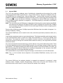
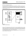
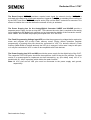
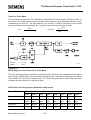
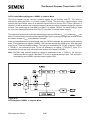
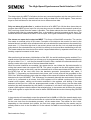
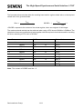
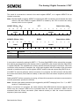
Clock Generator
The on-chip clock generator provides the C167 with its basic clock signal that controls all activities
of the controller hardware. Its oscillator can either run with an external crystal and appropriate
oscillator circuitry (see also recommendations in chapter „Dedicated Pins“) or it can be driven by an
external oscillator. The oscillator either directly feeds the external clock signal to the controller
hardware (through buffers, of course), divides the external clock frequency by 2, or feeds an on-chip
phase locked loop (PLL) which multiplies the input frequency by a selectable factor F (depending on
the device mode and/or type). This resulting internal clock signal is also referred to as “CPU clock”.
Two separated clock signals are generated for the CPU itself and the peripheral part of the chip.
While the CPU clock is stopped during the idle mode, the peripheral clock keeps running. Both
clocks are switched off, when the power down mode is entered.
The on-chip PLL circuit allows operation of the C167 on a low frequency external clock while still
providing maximum performance. The PLL multiplies the external clock frequency by a selectable
factor of 1:F and generates a CPU clock signal with 50% duty cycle. The PLL also provides fail safe
mechanisms which allow the detection of frequency deviations and the execution of emergency
actions in case of an external clock failure.
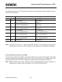
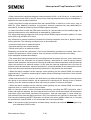
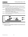
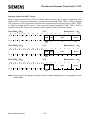
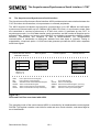
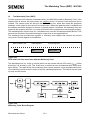
Figure 2-3
PLL Block Diagram
Semiconductor Group
2-9
Architectural Overview / C167
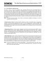
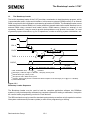
PLL Operation
The PLL is enabled when pin P0H.7 is latched high during reset. On power-up the PLL provides a
stable clock signal within ca. 1 ms after VCC has reached 5V±10%, even if there is no external clock
signal (in this case the PLL will run on its basic frequency of 2...5 MHz). The PLL starts
synchronizing with the external clock signal as soon as it is available. Within ca. 1 ms after stable
oscillations of the external clock within the specified frequency range the PLL will be synchronous
with this clock at a frequency of F * fOSC, ie. the PLL locks to the external clock.
Note: If the C167 is required to operate on the desired CPU clock directly after reset make sure that
RSTIN remains active until the PLL has locked (ca. 1 ms).
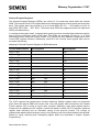
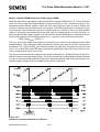
When PLL operation is selected the CPU clock is a selectable multiple of the oscillator frequency,
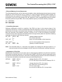
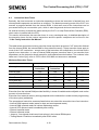
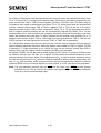
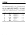
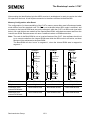
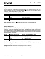
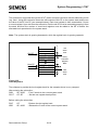
ie. the input frequency. The table below lists the possible selections.
P0.15-13
(P0H.7-5)
1)
2)
CPU
Frequency fCPU
= fXTAL * F
External Clock Input Notes
Range 1)
1
1
1
fXTAL * 4
2.5 to 6.25 MHz
1
1
0
fXTAL * 3
3.33 to 8.33 MHz
1
0
1
fXTAL * 2
5 to 12.5 MHz
1
0
0
fXTAL * 5
2 to 5 MHz
0
X
X
fXTAL * 1
1 to 25 MHz
Default configuration
Direct drive 2)
The external clock input range refers to a CPU clock range of 10...25 MHz.
The maximum depends on the duty cycle of the external clock signal.
In emulation mode direct drive is selected with P0.15 (P0H.7) = ’1’.
The PLL constantly synchronizes to the external clock signal. Due to the fact that the external
frequency is 1/F’th of the PLL output frequency the output frequency may be slightly higher or lower
than the desired frequency. This jitter is irrelevant for longer time periods. For short periods (1...4
CPU clock cycles) it remains below 4%.
When the PLL detects a missing input clock signal it generates an interrupt request. This warning
interrupt indicates that the PLL frequency is no more locked, ie. no more stable. This occurs when
the input clock is unstable and especially when the input clock fails completely, eg. due to a broken
crystal. In this case the synchronization mechanism will reduce the PLL output frequency down to
the PLL’s basic frequency (2...5 MHz). The basic frequency is still generated and allows the CPU to
execute emergency actions in case of a loss of the external clock.
Operation without PLL
The PLL is disabled when pin P0H.7 is latched low during reset. In this case the C167’s clock
system is directly fed from the external clock input, ie. fOSC = fCPU. The maximum input clock
frequency depends on the clock signal’s duty cycle, because the minimum values for the clock
phases (TCLs) must be respected.
Semiconductor Group
2-10
Architectural Overview / C167
2.3
The On-chip Peripheral Blocks
The C167 family clearly separates peripherals from the core. This structure permits the maximum
number of operations to be performed in parallel and allows peripherals to be added or deleted from
family members without modifications to the core. Each functional block processes data
independently and communicates information over common buses. Peripherals are controlled by
data written to the respective Special Function Registers (SFRs). These SFRs are located either
within the standard SFR area (00’FE00H...00’FFFFH) or within the extended ESFR area
(00’F000H...00’F1FFH).
These built in peripherals either allow the CPU to interface with the external world, or provide
functions on-chip that otherwise were to be added externally in the respective system.
The C167 generic peripherals are:
• Two General Purpose Timer Blocks (GPT1 and GPT2)
• Two Serial Interfaces (ASC0 and SSC)
• A Watchdog Timer
• Two 16-channel Capture / Compare units (CAPCOM1 and CAPCOM2)
• A 4-channel Pulse Width Modulation unit
• A 10-bit Analog / Digital Converter
• Nine IO ports with a total of 111 IO lines
Each peripheral also contains a set of Special Function Registers (SFRs), which control the
functionality of the peripheral and temporarily store intermediate data results. Each peripheral has
an associated set of status flags. Individually selected clock signals are generated for each
peripheral from binary multiples of the CPU clock.
Peripheral Interfaces
The on-chip peripherals generally have two different types of interfaces, an interface to the CPU
and an interface to external hardware. Communication between CPU and peripherals is performed
through Special Function Registers (SFRs) and interrupts. The SFRs serve as control/status and
data registers for the peripherals. Interrupt requests are generated by the peripherals based on
specific events which occur during their operation (eg. operation complete, error, etc.).
For interfacing with external hardware, specific pins of the parallel ports are used, when an input or
output function has been selected for a peripheral. During this time, the port pins are controlled by
the peripheral (when used as outputs) or by the external hardware which controls the peripheral
(when used as inputs). This is called the 'alternate (input or output) function' of a port pin, in contrast
to its function as a general purpose IO pin.
Peripheral Timing
Internal operation of CPU and peripherals is based on the CPU clock (f CPU). The on-chip oscillator
derives the CPU clock from the crystal or from the external clock signal. The clock signal which is
gated to the peripherals is independent from the clock signal which feeds the CPU. During Idle
mode the CPU’s clock is stopped while the peripherals continue their operation. Peripheral SFRs
may be accessed by the CPU once per state. When an SFR is written to by software in the same
state where it is also to be modified by the peripheral, the software write operation has priority.
Further details on peripheral timing are included in the specific sections about each peripheral.
Semiconductor Group
2-11
Architectural Overview / C167
Programming Hints
Access to SFRs
All SFRs reside in data page 3 of the memory space. The following addressing mechanisms allow
to access the SFRs:
• indirect or direct addressing with 16-bit (mem) addresses it must be guaranteed that the used
data page pointer (DPP0...DPP3) selects data page 3.
• accesses via the Peripheral Event Controller (PEC) use the SRCPx and DSTPx pointers instead
of the data page pointers.
• short 8-bit (reg) addresses to the standard SFR area do not use the data page pointers but
directly access the registers within this 512 Byte area.
• short 8-bit (reg) addresses to the extended ESFR area require switching to the 512 Byte
extended SFR area. This is done via the EXTension instructions EXTR, EXTP(R), EXTS(R).
Byte write operations to word wide SFRs via indirect or direct 16-bit (mem) addressing or byte
transfers via the PEC force zeros in the non-addressed byte. Byte write operations via short 8-bit
(reg) addressing can only access the low byte of an SFR and force zeros in the high byte. It is
therefore recommended, to use the bit field instructions (BFLDL and BFLDH) to write to any number
of bits in either byte of an SFR without disturbing the non-addressed byte and the unselected bits.
Reserved Bits
Some of the bits which are contained in the C167's SFRs are marked as 'Reserved'. User software
should never write '1's to reserved bits. These bits are currently not implemented and may be used
in future products to invoke new functions. In this case, the active state for these functions will be
'1', and the inactive state will be '0'. Therefore writing only ‘0’s to reserved locations provides
portability of the current software to future devices. Read accesses to reserved bits return ‘0’s.
Parallel Ports
The C167 provides up to 111 IO lines which are organized into eight input/output ports and one
input port. All port lines are bit-addressable, and all input/output lines are individually (bit-wise)
programmable as inputs or outputs via direction registers. The IO ports are true bidirectional ports
which are switched to high impedance state when configured as inputs. The output drivers of three
IO ports can be configured (pin by pin) for push/pull operation or open-drain operation via control
registers. During the internal reset, all port pins are configured as inputs.
All port lines have programmable alternate input or output functions associated with them. PORT0
and PORT1 may be used as address and data lines when accessing external memory, while Port 4
outputs the additional segment address bits A23/19/17...A16 in systems where segmentation is
used to access more than 64 KBytes of memory. Port 6 provides optional bus arbitration signals
(BREQ, HLDA, HOLD) and chip select signals. Port 2 accepts the fast external interrupt inputs and
provides inputs/outputs for the CAPCOM1 unit. Port 3 includes alternate functions of timers, serial
interfaces, the optional bus control signal BHE and the system clock output (CLKOUT). Port 5 is
used for timer control signals and for the analog inputs to the A/D Converter. Port 7 provides the
output signals from the PWM unit and inputs/outputs for the CAPCOM2 unit. Port 8 provides inputs/
outputs for the CAPCOM2 unit. Four pins of PORT1 may also be used as inputs for the CAPCOM2
unit. All port lines that are not used for these alternate functions may be used as general purpose
IO lines.
Semiconductor Group
2-12
Architectural Overview / C167
Serial Channels
Serial communication with other microcontrollers, processors, terminals or external peripheral
components is provided by two serial interfaces with different functionality, an Asynchronous/
Synchronous Serial Channel (ASC0) and a High-Speed Synchronous Serial Channel (SSC).
They are upward compatible with the serial ports of the Siemens 8-bit microcontroller families and
support full-duplex asynchronous communication at up to 625 KBaud and half-duplex synchronous
communication at up to 5 MBaud (2.5 MBaud on the ASC0) @ 20 MHz CPU clock. The SSC may
be configured so it interfaces with serially linked peripheral components.
Two dedicated baud rate generators allow to set up all standard baud rates without oscillator tuning.
For transmission, reception and error handling 3 separate interrupt vectors are provided on channel
SSC, 4 vectors are provided on channel ASC0.
In asynchronous mode, 8- or 9-bit data frames are transmitted or received, preceded by a start bit
and terminated by one or two stop bits. For multiprocessor communication, a mechanism to
distinguish address from data bytes has been included (8-bit data plus wake up bit mode).
In synchronous mode, the ASC0 transmits or receives bytes (8 bits) synchronously to a shift clock
which is generated by the ASC0. The SSC transmits or receives characters of 2...16 bits length
synchronously to a shift clock which can be generated by the SSC (master mode) or by an external
master (slave mode). The SSC can start shifting with the LSB or with the MSB, while the ASC0
always shifts the LSB first.
A loop back option is available for testing purposes.
A number of optional hardware error detection capabilities has been included to increase the
reliability of data transfers. A parity bit can automatically be generated on transmission or be
checked on reception. Framing error detection allows to recognize data frames with missing stop
bits. An overrun error will be generated, if the last character received has not been read out of the
receive buffer register at the time the reception of a new character is complete.
The On-chip CAN Module
The integrated CAN Module handles the completely autonomous transmission and reception of
CAN frames in accordance with the CAN specification V2.0 part B (active), ie. the on-chip
CAN Module can receive and transmit standard frames with 11-bit identifiers as well as extended
frames with 29-bit identifiers.
The module provides Full CAN functionality on up to 15 message objects. Message object 15 may
be configured for Basic CAN functionality. Both modes provide separate masks for acceptance
filtering which allows to accept a number of identifiers in Full CAN mode and also allows to disregard
a number of identifiers in Basic CAN mode. All message objects can be updated independent from
the other objects and are equipped for the maximum message length of 8 bytes.
The bit timing is derived from the XCLK and is programmable up to a data rate of 1 MBaud. The
CAN Module uses two pins to interface to a bus transceiver.
Note: The CAN Module is not part of all C167 derivatives. This description, of course, refers to
those devices only which incorporate a CAN Module.
Semiconductor Group
2-13
Architectural Overview / C167
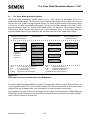
General Purpose Timer (GPT) Unit
The GPT units represent a very flexible multifunctional timer/counter structure which may be used
for many different time related tasks such as event timing and counting, pulse width and duty cycle
measurements, pulse generation, or pulse multiplication.
The five 16-bit timers are organized in two separate modules, GPT1 and GPT2. Each timer in each
module may operate independently in a number of different modes, or may be concatenated with
another timer of the same module.
Each timer can be configured individually for one of three basic modes of operation, which are
Timer, Gated Timer, and Counter Mode. In Timer Mode the input clock for a timer is derived from
the internal CPU clock divided by a programmable prescaler, while Counter Mode allows a timer to
be clocked in reference to external events (via TxIN).
Pulse width or duty cycle measurement is supported in Gated Timer Mode where the operation of
a timer is controlled by the ‘gate’ level on its external input pin TxIN.
The count direction (up/down) for each timer is programmable by software or may additionally be
altered dynamically by an external signal (TxEUD) to facilitate eg. position tracking.
The core timers T3 and T6 have output toggle latches (TxOTL) which change their state on each
timer over-flow/underflow. The state of these latches may be output on port pins (TxOUT) or may be
used internally to concatenate the core timers with the respective auxiliary timers resulting in 32/33bit timers/counters for measuring long time periods with high resolution.
Various reload or capture functions can be selected to reload timers or capture a timer’s contents
triggered by an external signal or a selectable transition of toggle latch TxOTL.
The maximum resolution of the timers in module GPT1 is 400 ns (@ 20 MHz CPU clock). With its
maximum resolution of 200 ns (@ 20 MHz CPU clock) the GPT2 timers provide precise event
control and time measurement.
Watchdog Timer
The Watchdog Timer represents one of the fail-safe mechanisms which have been implemented to
prevent the controller from malfunctioning for longer periods of time.
The Watchdog Timer is always enabled after a reset of the chip, and can only be disabled in the time
interval until the EINIT (end of initialization) instruction has been executed. Thus, the chip’s start-up
procedure is always monitored. The software has to be designed to service the Watchdog Timer
before it overflows. If, due to hardware or software related failures, the software fails to do so, the
Watchdog Timer overflows and generates an internal hardware reset and pulls the RSTOUT pin low
in order to allow external hardware components to reset.
The Watchdog Timer is a 16-bit timer, clocked with the CPU clock divided either by 2 or by 128. The
high byte of the Watchdog Timer register can be set to a prespecified reload value (stored in
WDTREL) in order to allow further variation of the monitored time interval. Each time it is serviced
by the application software, the high byte of the Watchdog Timer is reloaded. Thus, time intervals
between 25 µs and 420 ms can be monitored (@ 20 MHz). The default Watchdog Timer interval
after reset is 6.55 ms (@ 20 MHz).
Semiconductor Group
2-14
Architectural Overview / C167
Capture/Compare (CAPCOM) Units
The two CAPCOM units support generation and control of timing sequences on up to 32 channels
with a maximum resolution of 400 ns. The CAPCOM units are typically used to handle high speed
IO tasks such as pulse and waveform generation, pulse width modulation (PWM), Digital to Analog
(D/A) conversion, software timing, or time recording relative to external events.
Four 16-bit timers (T0/T1, T7/T8) with reload registers provide two independent time bases for the
capture/compare register array.
The input clock for the timers is programmable to several prescaled values of the internal CPU
clock, or may be derived from an overflow/underflow of timer T6 in module GPT2. This provides a
wide range of variation for the timer period and resolution and allows precise adjustments to the
application specific requirements. In addition, external count inputs for CAPCOM timers T0 and T7
allow event scheduling for the capture/compare registers relative to external events.
Both of the two capture/compare register arrays contain 16 dual purpose capture/compare
registers, each of which may be individually allocated to either CAPCOM timer T0 or T1 (T7 or T8,
respectively), and programmed for capture or compare function. Each register has one port pin
associated with it which serves as an input pin for triggering the capture function, or as an output pin
(except for CC24...CC27) to indicate the occurence of a compare event.
When a capture/compare register has been selected for capture mode, the current contents of the
allocated timer will be latched (captured) into the capture/compare register in response to an
external event at the port pin which is associated with this register. In addition, a specific interrupt
request for this capture/compare register is generated. Either a positive, a negative, or both a
positive and a negative external signal transition at the pin can be selected as the triggering event.
The contents of all registers which have been selected for one of the five compare modes are
continuously compared with the contents of the allocated timers. When a match occurs between the
timer value and the value in a capture/compare register, specific actions will be taken based on the
selected compare mode.
Pulse Width Modulation Unit
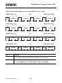
The PWM Unit supports the generation of up to four independent high-speed PWM signals. It allows
to generate standard (edge aligned) PWM signals as well as symmetrical (center aligned) PWM
signals. In Burst Mode two channels may be combined with their output signals ANDed, where one
channel gates the output signal of the other channel. Single Shot Mode allows to generate single
output pulses (retriggerable) under software control. Each PWM channel is controlled by an up/
down counter with associated reload and compare registers. The polarity of the PWM output signals
may be controlled via the respective port output latch (combination via EXOR).
Semiconductor Group
2-15
Architectural Overview / C167
A/D Converter
For analog signal measurement, a 10-bit A/D converter with 16 multiplexed input channels and a
sample and hold circuit has been integrated on-chip. It uses the method of successive
approximation. The sample time (for loading the capacitors) and the conversion time is
programmable and can so be adjusted to the external circuitry.
Overrun error detection/protection is provided for the conversion result register (ADDAT): either an
interrupt request will be generated when the result of a previous conversion has not been read from
the result register at the time the next conversion is complete, or the next conversion is suspended
in such a case until the previous result has been read.
For applications which require less than 16 analog input channels, the remaining channel inputs can
be used as digital input port pins.
The A/D converter of the C167 supports four different conversion modes. In the standard Single
Channel conversion mode, the analog level on a specified channel is sampled once and converted
to a digital result. In the Single Channel Continuous mode, the analog level on a specified channel
is repeatedly sampled and converted without software intervention. In the Auto Scan mode, the
analog levels on a prespecified number of channels are sequentially sampled and converted. In the
Auto Scan Continuous mode, the number of prespecified channels is repeatedly sampled and
converted. In addition, the conversion of a specific channel can be inserted (injected) into a running
sequence without disturbing this sequence. This is called Channel Injection Mode.
The Peripheral Event Controller (PEC) may be used to automatically store the conversion results
into a table in memory for later evaluation, without requiring the overhead of entering and exiting
interrupt routines for each data transfer.
Semiconductor Group
2-16
Architectural Overview / C167
2.4
Protected Bits
The C167 provides a special mechanism to protect bits which can be modified by the on-chip
hardware from being changed unintentionally by software accesses to related bits (see also chapter
“The Central Processing Unit”).
The following bits are protected:
Register
Bit Name
Notes
T2IC, T3IC, T4IC
T2IR, T3IR, T4IR
GPT1 timer interrupt request flags
T5IC, T6IC
T5IR, T6IR
GPT2 timer interrupt request flags
CRIC
CRIR
GPT2 CAPREL interrupt request flag
T3CON, T6CON
T3OTL, T6OTL
GPTx timer output toggle latches
T0IC, T1IC
T0IR, T1IR
CAPCOM1 timer interrupt request flags
T7IC, T8IC
T7IR, T8IR
CAPCOM2 timer interrupt request flags
S0TIC, S0TBIC
S0TIR, S0TBIR
ASC0 transmit(buffer) interrupt request flags
S0RIC, S0EIC
S0RIR, S0EIR
ASC0 receive/error interrupt request flags
S0CON
S0REN
ASC0 receiver enable flag
SSCTIC, SSCRIC
SSCTIR, SSCRIR
SSC transmit/receive interrupt request flags
SSCEIC
SSCEIR
SSC error interrupt request flag
SSCCON
SSCBSY
SSC busy flag
SSCCON
SSCBE, SSCPE
SSC error flags
SSCCON
SSCRE, SSCTE
SSC error flags
ADCIC, ADEIC
ADCIR, ADEIR
ADC end-of-conv./overrun intr. request flag
ADCON
ADST, ADCRQ
ADC start flag / injection request flag
CC31IC...CC16IC
CC31IR...CC16IR
CAPCOM2 interrupt request flags
CC15IC...CC0IC
CC15IR...CC0IR
CAPCOM1 interrupt request flags
PWMIC
PWMIR
PWM module interrupt request flag
TFR
TFR.15,14,13
Class A trap flags
TFR
TFR.7,3,2,1,0
Class B trap flags
P2
P2.15...P2.0
All bits of Port 2
P7
P7.7...P7.0
All bits of Port 7
P8
P8.7...P8.0
All bits of Port 8
XPyIC (y=3...0)
XPyIR (y=3...0)
X-Peripheral y interrupt request flag
Σ = 106 protected bits.
Semiconductor Group
2-17
Memory Organization / C167
3
Memory Organization
The memory space of the C167 is configured in a “Von Neumann” architecture. This means that
code and data are accessed within the same linear address space. All of the physically separated
memory areas, including internal ROM/Flash (where integrated), internal RAM, the internal Special
Function Register Areas (SFRs and ESFRs), the address areas for integrated XBUS peripherals
(eg. XRAM or CAN module) and external memory are mapped into one common address space.
The C167 provides a total addressable memory space of 16 MBytes. This address space is
arranged as 256 segments of 64 KBytes each, and each segment is again subdivided into four data
pages of 16 KBytes each (see figure below).
Figure 3-1
Memory Areas and Address Space
Semiconductor Group
3-1
Memory Organization / C167
Most internal memory areas are mapped into segment 0, the system segment. The upper 4 KByte
of segment 0 (00’F000H...00’FFFFH) hold the Internal RAM and Special Function Register Areas
(SFR and ESFR). The lower 32 KByte of segment 0 (00’0000H...00’7FFFH) may be occupied by a
part of the on-chip ROM or Flash memory and is called the Internal ROM area. This ROM area can
be remapped to segment 1 (01’0000 H...01’7FFFH), to enable external memory access in the lower
half of segment 0, or the internal ROM may be disabled at all.
Code and data may be stored in any part of the internal memory areas, except for the SFR blocks,
which may be used for control / data, but not for instructions.
Note: Accesses to the internal ROM area on ROMless devices will produce unpredictable results.
Bytes are stored at even or odd byte addresses. Words are stored in ascending memory locations
with the low byte at an even byte address being followed by the high byte at the next odd byte
address. Double words (code only) are stored in ascending memory locations as two subsequent
words. Single bits are always stored in the specified bit position at a word address. Bit position 0 is
the least significant bit of the byte at an even byte address, and bit position 15 is the most significant
bit of the byte at the next odd byte address. Bit addressing is supported for a part of the Special
Function Registers, a part of the internal RAM and for the General Purpose Registers.
Figure 3-2
Storage of Words, Byte and Bits in a Byte Organized Memory
Note: Byte units forming a single word or a double word must always be stored within the same
physical (internal, external, ROM, RAM) and organizational (page, segment) memory area.
Semiconductor Group
3-2
Memory Organization / C167
3.1
Internal ROM
The C167 may reserve an address area of variable size (depending on the version) for on-chip
mask-programmable ROM (organized as X * 32) or Flash memory. The lower 32 KByte of the onchip ROM/Flash are referred to as “Internal ROM Area”. Internal ROM accesses are globally
enabled or disabled via bit ROMEN in register SYSCON. This bit is set during reset according to the
level on pin EA, or may be altered via software. If enabled, the internal ROM area occupies the
lower 32 KByte of either segment 0 or segment 1. This ROM mapping is controlled by bit ROMS1
in register SYSCON.
Note: The size of the internal ROM area is independent of the size of the actual implemented ROM.
Also devices with less than 32 KByte of ROM or with no ROM at all will have this 32 KByte
area occupied, if the ROM is enabled. Devices with larger ROMs provide the mapping option
only for the ROM area.
Devices with a ROM size above 32 KByte expand the ROM area from the middle of segment 1, ie.
starting at address 01’8000H.
The internal ROM/Flash can be used for both code (instructions) and data (constants, tables, etc.)
storage.
Code fetches are always made on even byte addresses. The highest possible code storage location
in the internal ROM is either xx’xxFEH for single word instructions, or xx’xxFCH for double word
instructions. The respective location must contain a branch instruction (unconditional), because
sequential boundary crossing from internal ROM to external memory is not supported and causes
erroneous results.
Any word and byte data read accesses may use the indirect or long 16-bit addressing modes. There
is no short addressing mode for internal ROM operands. Any word data access is made to an even
byte address. The highest possible word data storage location in the internal ROM is xx’xxFEH. For
PEC data transfers the internal ROM can be accessed independent of the contents of the DPP
registers via the PEC source and destination pointers.
The internal ROM is not provided for single bit storage, and therefore it is not bit addressable.
Note: The ‘x’ in the locations above depend on the available ROM/Flash memory and on the
mapping.
The internal ROM may be enabled, disabled or mapped into segment 0 or segment 1 under
software control. Chapter “System Programming” shows how to do this and reminds of the
precautions that must be taken in order to prevent the system from crashing.
Semiconductor Group
3-3
Memory Organization / C167
3.2
Internal RAM and SFR Area
The RAM/SFR area is located within data page 3 and provides access to 2 KByte of on-chip RAM
(organized as 1K*16) and to two 512 Byte blocks of Special Function Registers (SFRs).
The internal RAM serves for several purposes:
• System Stack (programmable size)
• General Purpose Register Banks (GPRs)
• Source and destination pointers for the Peripheral Event Controller (PEC)
• Variable and other data storage, or
• Code storage.
Figure 3-3
Internal RAM Area and SFR Areas
Note: The upper 256 bytes of SFR area, ESFR area and internal RAM are bit-addressable (see
shaded blocks in the figure above).
Semiconductor Group
3-4
Memory Organization / C167
Code accesses are always made on even byte addresses. The highest possible code storage
location in the internal RAM is either 00’FDFE H for single word instructions or 00’FDFCH for double
word instructions. The respective location must contain a branch instruction (unconditional),
because sequential boundary crossing from internal RAM to the SFR area is not supported and
causes erroneous results.
Any word and byte data in the internal RAM can be accessed via indirect or long 16-bit addressing
modes, if the selected DPP register points to data page 3. Any word data access is made on an
even byte address. The highest possible word data storage location in the internal RAM is
00’FDFEH. For PEC data transfers, the internal RAM can be accessed independent of the contents
of the DPP registers via the PEC source and destination pointers.
The upper 256 Byte of the internal RAM (00’FD00H through 00’FDFFH) and the GPRs of the current
bank are provided for single bit storage, and thus they are bit addressable.
System Stack
The system stack may be defined within the internal RAM. The size of the system stack is controlled
by bitfield STKSZ in register SYSCON (see table below).
<STKSZ>
Stack Size (Words)
Internal RAM Addresses (Words)
000B
256
00’FBFEH...00’FA00H (Default after Reset)
001B
128
00’FBFEH...00’FB00H
010B
64
00’FBFEH...00’FB80H
011B
32
00’FBFEH...00’FBC0H
100B
512
00’FBFEH...00’F800H
101B
---
Reserved. Do not use this combination.
110B
---
Reserved. Do not use this combination.
111B
1024
00’FDFEH...00’F600H (Note: No circular stack)
For all system stack operations the on-chip RAM is accessed via the Stack Pointer (SP) register.
The stack grows downward from higher towards lower RAM address locations. Only word accesses
are supported to the system stack. A stack overflow (STKOV) and a stack underflow (STKUN)
register are provided to control the lower and upper limits of the selected stack area. These two
stack boundary registers can be used not only for protection against data destruction, but also allow
to implement a circular stack with hardware supported system stack flushing and filling (except for
the 2KByte stack option).
The technique of implementing this circular stack is described in chapter “System Programming”.
Semiconductor Group
3-5
Memory Organization / C167
General Purpose Registers
The General Purpose Registers (GPRs) use a block of 16 consecutive words within the internal
RAM. The Context Pointer (CP) register determines the base address of the currently active register
bank. This register bank may consist of up to 16 word GPRs (R0, R1, ..., R15) and/or of up to 16
byte GPRs (RL0, RH0, ..., RL7, RH7). The sixteen byte GPRs are mapped onto the first eight word
GPRs (see table below).
In contrast to the system stack, a register bank grows from lower towards higher address locations
and occupies a maximum space of 32 bytes. The GPRs are accessed via short 2-, 4- or 8-bit
addressing modes using the Context Pointer (CP) register as base address (independent of the
current DPP register contents). Additionally, each bit in the currently active register bank can be
accessed individually.
Mapping of General Purpose Registers to RAM Addresses
Internal RAM Address
Byte Registers
Word Register
<CP> + 1EH
---
R15
<CP> + 1CH
---
R14
<CP> + 1AH
---
R13
<CP> + 18H
---
R12
<CP> + 16H
---
R11
<CP> + 14H
---
R10
<CP> + 12H
---
R9
<CP> + 10H
---
R8
<CP> + 0EH
RH7
RL7
R7
<CP> + 0CH
RH6
RL6
R6
<CP> + 0AH
RH5
RL5
R5
<CP> + 08H
RH4
RL4
R4
<CP> + 06H
RH3
RL3
R3
<CP> + 04H
RH2
RL2
R2
<CP> + 02H
RH1
RL1
R1
<CP> + 00H
RH0
RL0
R0
The C167 supports fast register bank (context) switching. Multiple register banks can physically
exist within the internal RAM at the same time. Only the register bank selected by the Context
Pointer register (CP) is active at a given time, however. Selecting a new active register bank is
simply done by updating the CP register. A particular Switch Context (SCXT) instruction performs
register bank switching and an automatic saving of the previous context. The number of
implemented register banks (arbitrary sizes) is only limited by the size of the available internal RAM.
Details on using, switching and overlapping register banks are described in chapter “System
Programming”.
Semiconductor Group
3-6
Memory Organization / C167
PEC Source and Destination Pointers
The 16 word locations in the internal RAM from 00’FCE0 H to 00’FCFEH (just below the bitaddressable section) are provided as source and destination address pointers for data transfers on
the eight PEC channels. Each channel uses a pair of pointers stored in two subsequent word
locations with the source pointer (SRCPx) on the lower and the destination pointer (DSTPx) on the
higher word address (x = 7...0).
Figure 3-4
Location of the PEC Pointers
Whenever a PEC data transfer is performed, the pair of source and destination pointers, which is
selected by the specified PEC channel number, is accessed independent of the current DPP
register contents and also the locations referred to by these pointers are accessed independent of
the current DPP register contents. If a PEC channel is not used, the corresponding pointer locations
area available and can be used for word or byte data storage.
For more details about the use of the source and destination pointers for PEC data transfers see
section “Interrupt and Trap Functions”.
Semiconductor Group
3-7
Memory Organization / C167
Special Function Registers
The functions of the CPU, the bus interface, the IO ports and the on-chip peripherals of the C167 are
controlled via a number of so-called Special Function Registers (SFRs). These SFRs are arranged
within two areas of 512 Byte size each. The first register block, the SFR area, is located in the 512
Bytes above the internal RAM (00’FFFFH...00’FE00H), the second register block, the Extended SFR
(ESFR) area, is located in the 512 Bytes below the internal RAM (00’F1FFH...00’F000H).
Special function registers can be addressed via indirect and long 16-bit addressing modes. Using
an 8-bit offset together with an implicit base address allows to address word SFRs and their
respective low bytes. However, this does not work for the respective high bytes!
Note: Writing to any byte of an SFR causes the non-addressed complementary byte to be cleared!
The upper half of each register block is bit-addressable, so the respective control/status bits can
directly be modified or checked using bit addressing.
When accessing registers in the ESFR area using 8-bit addresses or direct bit addressing, an
Extend Register (EXTR) instruction is required before, to switch the short addressing mechanism
from the standard SFR area to the Extended SFR area. This is not required for 16-bit and indirect
addresses. The GPRs R15...R0 are duplicated, ie. they are accessible within both register blocks
via short 2-, 4- or 8-bit addresses without switching.
Example:
EXTR
MOV
BFLDL
BSET
MOV
#4
ODP2, #data16
DP6, #mask, #data8
DP1H.7
T8REL, R1
;Switch to ESFR area for the next 4 instructions
;ODP2 uses 8-bit reg addressing
;Bit addressing for bit fields
;Bit addressing for single bits
;T8REL uses 16-bit address, R1 is duplicated...
;...and also accessible via the ESFR mode
;(EXTR is not required for this access)
;-------
;-------------------
;The scope of the EXTR #4 instruction ends here!
MOV
T8REL, R1
;T8REL uses 16-bit address, R1 is duplicated...
;...and does not require switching
In order to minimize the use of the EXTR instructions the ESFR area mostly holds registers which
are mainly required for initialization and mode selection. Registers that need to be accessed
frequently are allocated to the standard SFR area, wherever possible.
Note: The tools are equipped to monitor accesses to the ESFR area and will automatically insert
EXTR instructions, or issue a warning in case of missing or excessive EXTR instructions.
Semiconductor Group
3-8
Memory Organization / C167
3.3
The On-Chip XRAM
The XRAM area is located within data page 3 and provides access to 2 KByte of on-chip RAM
(organized as 1K*16). As the XRAM is connected to the internal XBUS it is accessed like external
memory, however, no external bus cycles are executed for these accesses. XRAM accesses are
globally enabled or disabled via bit XPEN in register SYSCON. This bit is cleared after reset and
may be set via software during the initialization to allow accesses to the on-chip XRAM. When the
XRAM is disabled (default after reset) all accesses to the XRAM area are mapped to external
locations. The XRAM may be used for both code (instructions) and data (variables, user stack,
tables, etc.) storage.
Code fetches are always made on even byte addresses. The highest possible code storage location
in the XRAM is either 00’E7FEH for single word instructions, or 00’E7FCH for double word
instructions. The respective location must contain a branch instruction (unconditional), because
sequential boundary crossing from XRAM to external memory is not supported and causes
erroneous results.
Any word and byte data read accesses may use the indirect or long 16-bit addressing modes. There
is no short addressing mode for XRAM operands. Any word data access is made to an even byte
address. The highest possible word data storage location in the XRAM is 00’E7FEH. For PEC data
transfers the XRAM can be accessed independent of the contents of the DPP registers via the PEC
source and destination pointers.
Note: As the XRAM appears like external memory it cannot be used for the C167’s system stack
or register banks. The XRAM is not provided for single bit storage and therefore is not bit
addressable.
The on-chip XRAM is accessed without any waitstates using 16-bit demultiplexed bus cycles which
take 100 ns (@ 20 MHz fCPU). Even if the XRAM is used like external memory it does not occupy
BUSCONx/ADDRSELx registers but rather is selected via additional dedicated XBCON/XADRS
registers. These registers are mask-programmed and are not user accessible. With these registers
the address area 00’E000H to 00’E7FFH is reserved for XRAM accesses.
XRAM Access via External Masters
When bit XPER-SHARE in register SYSCON is set the on-chip XRAM of the C167 can be accessed
by an external master during hold mode via the C167’s bus interface. These external accesses
must use the same configuration as internally programmed, ie. demultiplexed bus, 100 ns minimum
access cycle time. No waitstates are required.
Note: The configuration in register SYSCON cannot be changed after the execution of the EINIT
instruction.
Semiconductor Group
3-9
Memory Organization / C167
Figure 3-5
On-chip XRAM Area
Note: The address area 00’E800H to 00’EEFFH is mapped to external memory but should be
reserved for reasons of upward compatibility.
Semiconductor Group
3-10
Memory Organization / C167
3.4
External Memory Space
The C167 is capable of using an address space of up to 16 MByte. Only parts of this address space
are occupied by internal memory areas. All addresses which are not used for on-chip memory
(ROM or RAM) or for registers may reference external memory locations. This external memory is
accessed via the C167’s external bus interface.
Four memory bank sizes are supported:
• Non-segmented mode: 64 KByte
• 2-bit segmented mode: 256 KByte
• 4-bit segmented mode: 1 MByte
• 8-bit segmented mode: 16 MByte
with A15...A0 on PORT0 or PORT1
with A17...A16 on Port 4 and A15...A0 on PORT0 or PORT1
with A19...A16 on Port 4 and A15...A0 on PORT0 or PORT1
with A23...A16 on Port 4 and A15...A0 on PORT0 or PORT1
Each bank can be directly addressed via the address bus, while the programmable chip select
signals can be used to select various memory banks.
The C167 also supports four different bus types:
• Multiplexed 16-bit Bus
• Multiplexed 8-bit Bus
• Demultiplexed 16-bit Bus
• Demultiplexed 8-bit Bus
with address and data on PORT0 (Default after Reset)
with address and data on PORT0/P0L
with address on PORT1 and data on PORT0
with address on PORT1 and data on P0L
Memory model and bus mode are selected during reset by pin EA and PORT0 pins. For further
details about the external bus configuration and control please refer to chapter "The External Bus
Interface".
External word and byte data can only be accessed via indirect or long 16-bit addressing modes
using one of the four DPP registers. There is no short addressing mode for external operands. Any
word data access is made to an even byte address.
For PEC data transfers the external memory in segment 0 can be accessed independent of the
contents of the DPP registers via the PEC source and destination pointers.
The external memory is not provided for single bit storage and therefore it is not bit addressable.
Semiconductor Group
3-11
Memory Organization / C167
3.5
Crossing Memory Boundaries
The address space of the C167 is implicitly divided into equally sized blocks of different granularity
and into logical memory areas. Crossing the boundaries between these blocks (code or data) or
areas requires special attention to ensure that the controller executes the desired operations.
Memory Areas are partitions of the address space that represent different kinds of memory (if
provided at all). These memory areas are the internal RAM/SFR area, the internal ROM (if
available), the on-chip X-Peripherals (if integrated) and the external memory.
Accessing subsequent data locations that belong to different memory areas is no problem.
However, when executing code, the different memory areas must be switched explicitly via branch
instructions. Sequential boundary crossing is not supported and leads to erroneous results.
Note: Changing from the external memory area to the internal RAM/SFR area takes place within
segment 0.
Segments are contiguous blocks of 64 KByte each. They are referenced via the code segment
pointer CSP for code fetches and via an explicit segment number for data accesses overriding the
standard DPP scheme.
During code fetching segments are not changed automatically, but rather must be switched
explicitly. The instructions JMPS, CALLS and RETS will do this.
In larger sequential programs make sure that the highest used code location of a segment contains
an unconditional branch instruction to the respective following segment, to prevent the prefetcher
from trying to leave the current segment.
Data Pages are contiguous blocks of 16 KByte each. They are referenced via the data page
pointers DPP3...0 and via an explicit data page number for data accesses overriding the standard
DPP scheme. Each DPP register can select one of the possible 1024 data pages. The DPP register
that is used for the current access is selected via the two upper bits of the 16-bit data address.
Subsequent 16-bit data addresses that cross the 16 KByte data page boundaries therefore will use
different data page pointers, while the physical locations need not be subsequent within memory.
Semiconductor Group
3-12
The Central Processing Unit (CPU) / C167
4
The Central Processing Unit (CPU)
Basic tasks of the CPU are to fetch and decode instructions, to supply operands for the arithmetic
and logic unit (ALU), to perform operations on these operands in the ALU, and to store the
previously calculated results. As the CPU is the main engine of the C167 controller, it is also
affected by certain actions of the peripheral subsystem.
Since a four stage pipeline is implemented in the C167, up to four instructions can be processed in
parallel. Most instructions of the C167 are executed in one machine cycle (ie. 100 ns @ 20 MHz
CPU clock) due to this parallelism. This chapter describes how the pipeline works for sequential and
branch instructions in general, and which hardware provisions have been made to speed the
execution of jump instructions in particular. The general instruction timing is described including
standard and exceptional timing.
While internal memory accesses are normally performed by the CPU itself, external peripheral or
memory accesses are performed by a particular on-chip External Bus Controller (EBC), which is
automatically invoked by the CPU whenever a code or data address refers to the external address
space. If possible, the CPU continues operating while an external memory access is in progress. If
external data are required but are not yet available, or if a new external memory access is requested
by the CPU, before a previous access has been completed, the CPU will be held by the EBC until
the request can be satisfied. The EBC is described in a dedicated chapter.
Figure 4-1
CPU Block Diagram
Semiconductor Group
4-1
The Central Processing Unit (CPU) / C167
The on-chip peripheral units of the C167 work nearly independent of the CPU with a separate clock
generator. Data and control information is interchanged between the CPU and these peripherals via
Special Function Registers (SFRs). Whenever peripherals need a non-deterministic CPU action, an
on-chip Interrupt Controller compares all pending peripheral service requests against each other
and prioritizes one of them. If the priority of the current CPU operation is lower than the priority of
the selected peripheral request, an interrupt will occur.
Basically, there are two types of interrupt processing:
• Standard interrupt processing forces the CPU to save the current program status and the return
address on the stack before branching to the interrupt vector jump table.
• PEC interrupt processing steals just one machine cycle from the current CPU activity to perform
a single data transfer via the on-chip Peripheral Event Controller (PEC).
System errors detected during program execution (socalled hardware traps) or an external nonmaskable interrupt are also processed as standard interrupts with a very high priority.
In contrast to other on-chip peripherals, there is a closer conjunction between the watchdog timer
and the CPU. If enabled, the watchdog timer expects to be serviced by the CPU within a
programmable period of time, otherwise it will reset the chip. Thus, the watchdog timer is able to
prevent the CPU from going totally astray when executing erroneous code. After reset, the
watchdog timer starts counting automatically, but it can be disabled via software, if desired.
Beside its normal operation there are the following particular CPU states:
• Reset state: Any reset (hardware, software, watchdog) forces the CPU into a predefined active
state.
• IDLE state: The clock signal to the CPU itself is switched off, while the clocks for the on-chip
peripherals keep running.
• POWER DOWN state: All of the on-chip clocks are switched off.
A transition into an active CPU state is forced by an interrupt (if being IDLE) or by a reset (if being
in POWER DOWN mode).
The IDLE, POWER DOWN and RESET states can be entered by particular C167 system control
instructions.
A set of Special Function Registers is dedicated to the functions of the CPU core:
•
•
•
•
•
•
•
•
General System Configuration
CPU Status Indication and Control
Code Access Control
Data Paging Control
GPRs Access Control
System Stack Access Control
Multiply and Divide Support
ALU Constants Support
Semiconductor Group
: SYSCON (RP0H)
: PSW
: IP, CSP
: DPP0, DPP1, DPP2, DPP3
: CP
: SP, STKUN, STKOV
: MDL, MDH, MDC
: ZEROS, ONES
4-2
The Central Processing Unit (CPU) / C167
4.1
Instruction Pipelining
The instruction pipeline of the C167 partitiones instruction processing into four stages of which each
one has its individual task:
1st –>FETCH:
In this stage the instruction selected by the Instruction Pointer (IP) and the Code Segment Pointer
(CSP) is fetched from either the internal ROM, internal RAM, or external memory.
2nd –>DECODE:
In this stage the instructions are decoded and, if required, the operand addresses are calculated
and the respective operands are fetched. For all instructions, which implicitly access the system
stack, the SP register is either decremented or incremented, as specified. For branch instructions
the Instruction Pointer and the Code Segment Pointer are updated with the desired branch target
address (provided that the branch is taken).
3rd –>EXECUTE:
In this stage an operation is performed on the previously fetched operands in the ALU. Additionally,
the condition flags in the PSW register are updated as specified by the instruction. All explicit writes
to the SFR memory space and all auto-increment or auto-decrement writes to GPRs used as
indirect address pointers are performed during the execute stage of an instruction, too.
4th –>WRITE BACK:
In this stage all external operands and the remaining operands within the internal RAM space are
written back.
A particularity of the C167 are the so-called injected instructions. These injected instructions are
generated internally by the machine to provide the time needed to process instructions, which
cannot be processed within one machine cycle. They are automatically injected into the decode
stage of the pipeline, and then they pass through the remaining stages like every standard
instruction. Program interrupts are performed by means of injected instructions, too. Although these
internally injected instructions will not be noticed in reality, they are introduced here to ease the
explanation of the pipeline in the following.
Sequential Instruction Processing
Each single instruction has to pass through each of the four pipeline stages regardless of whether
all possible stage operations are really performed or not. Since passing through one pipeline stage
takes at least one machine cycle, any isolated instruction takes at least four machine cycles to be
completed. Pipelining, however, allows parallel (ie. simultaneous) processing of up to four
instructions. Thus, most of the instructions seem to be processed during one machine cycle as soon
as the pipeline has been filled once after reset (see figure below).
Instruction pipelining increases the average instruction throughput considered over a certain period
of time. In the following, any execution time specification of an instruction always refers to the
average execution time due to pipelined parallel instruction processing.
Semiconductor Group
4-3
The Central Processing Unit (CPU) / C167
1 Machine
Cycle
FETCH
I1
DECODE
I2
I3
I4
I5
I6
I1
I2
I3
I4
I5
I1
I2
I3
I4
I1
I2
I3
EXECUTE
WRITEBACK
time
Figure 4-2
Sequential Instruction Pipelining
Standard Branch Instruction Processing
Instruction pipelining helps to speed sequential program processing. In the case that a branch is
taken, the instruction which has already been fetched providently is mostly not the instruction which
must be decoded next. Thus, at least one additional machine cycle is normally required to fetch the
branch target instruction. This extra machine cycle is provided by means of an injected instruction
(see figure below).
Injection
1 Machine
Cycle
FETCH
BRANCH
In+2
ITARGET
ITARGET+1 ITARGET+2 ITARGET+3
DECODE
In
BRANCH
(IINJECT)
ITARGET
EXECUTE
...
In
BRANCH
(IINJECT)
ITARGET
ITARGET+1
WRITEBACK
...
...
In
BRANCH
(IINJECT)
ITARGET
ITARGET+1 ITARGET+2
time
Figure 4-3
Standard Branch Instruction Pipelining
If a conditional branch is not taken, there is no deviation from the sequential program flow, and thus
no extra time is required. In this case the instruction after the branch instruction will enter the decode
stage of the pipeline at the beginning of the next machine cycle after decode of the conditional
branch instruction.
Semiconductor Group
4-4
The Central Processing Unit (CPU) / C167
Cache Jump Instruction Processing
The C167 incorporates a jump cache to optimize conditional jumps, which are processed
repeatedly within a loop. Whenever a jump on cache is taken, the extra time to fetch the branch
target instruction can be saved and thus the corresponding cache jump instruction in most cases
takes only one machine cycle.
This performance is achieved by the following mechanism:
Whenever a cache jump instruction passes through the decode stage of the pipeline for the first
time (and provided that the jump condition is met), the jump target instruction is fetched as usual,
causing a time delay of one machine cycle. In contrast to standard branch instructions, however, the
target instruction of a cache jump instruction (JMPA, JMPR, JB, JBC, JNB, JNBS) is additionally
stored in the cache after having been fetched.
After each repeatedly following execution of the same cache jump instruction, the jump target
instruction is not fetched from progam memory but taken from the cache and immediatly injected
into the decode stage of the pipeline (see figure below).
A time saving jump on cache is always taken after the second and any further occurrence of the
same cache jump instruction, unless an instruction which, has the fundamental capability of
changing the CSP register contents (JMPS, CALLS, RETS, TRAP, RETI), or any standard interrupt
has been processed during the period of time between two following occurrences of the same
cache jump instruction.
1 Machine
Cycle
FETCH
DECODE
In+2
ITARGET
Cache Jmp (IINJECT)
EXECUTE
In
WRITEBACK
...
Injection of cached
Target Instruction
Injection
ITARGET+1
In+2
ITARGET
Cache Jmp
ITARGET
ITARGET+1
In
Cache Jmp
ITARGET
...
In
Cache Jmp
Cache Jmp (IINJECT)
In
Cache Jmp
1st loop iteration
Repeated loop iteration
Figure 4-4
Cache Jump Instruction Pipelining
Semiconductor Group
ITARGET+1 ITARGET+2
4-5
The Central Processing Unit (CPU) / C167
Particular Pipeline Effects
Since up to four different instructions are processed simultaneously, additional hardware has been
spent in the C167 to consider all causal dependencies which may exist on instructions in different
pipeline stages without a loss of performance. This extra hardware (ie. for ’forwarding’ operand read
and write values) resolves most of the possible conflicts (eg. multiple usage of buses) in a time
optimized way and thus avoids that the pipeline becomes noticeable for the user in most cases.
However, there are some very rare cases, where the circumstance that the C167 is a pipelined
machine requires attention by the programmer. In these cases the delays caused by pipeline
conflicts can be used for other instructions in order to optimize performance.
• Context Pointer Updating
An instruction, which calculates a physical GPR operand address via the CP register, is mostly not
capable of using a new CP value, which is to be updated by an immediately preceding instruction.
Thus, to make sure that the new CP value is used, at least one instruction must be inserted between
a CP-changing and a subsequent GPR-using instruction, as shown in the following example:
In
In+1
In+2
: SCXT CP, #0FC00h
: ....
: MOV R0, #dataX
; select a new context
; must not be an instruction using a GPR
; write to GPR 0 in the new context
• Data Page Pointer Updating
An instruction, which calculates a physical operand address via a particular DPPn (n=0 to 3)
register, is mostly not capable of using a new DPPn register value, which is to be updated by an
immediately preceding instruction. Thus, to make sure that the new DPPn register value is used, at
least one instruction must be inserted between a DPPn-changing instruction and a subsequent
instruction which implicitly uses DPPn via a long or indirect addressing mode, as shown in the
following example:
In
In+1
In+2
: MOV DPP0, #4
: ....
: MOV DPP0:0000H, R1
; select data page 4 via DPP0
; must not be an instruction using DPP0
; move contents of R1 to address location 01’0000 H
; (in data page 4) supposed segmentation is enabled
• Explicit Stack Pointer Updating
None of the RET, RETI, RETS, RETP or POP instructions is capable of correctly using a new SP
register value, which is to be updated by an immediately preceding instruction. Thus, in order to use
the new SP register value without erroneously performed stack accesses, at least one instruction
must be inserted between an explicitly SP-writing and any subsequent of the just mentioned
implicitly SP-using instructions, as shown in the following example:
In
In+1
: MOV SP, #0FA40H
: ....
In+2
: POP R0
Semiconductor Group
; select a new top of stack
; must not be an instruction popping operands
; from the system stack
; pop word value from new top of stack into R0
4-6
The Central Processing Unit (CPU) / C167
• External Memory Access Sequences
The effect described here will only become noticeable, when watching the external memory access
sequences on the external bus (eg. by means of a Logic Analyzer). Different pipeline stages can
simultaneously put a request on the External Bus Controller (EBC). The sequence of instructions
processed by the CPU may diverge from the sequence of the corresponding external memory
accesses performed by the EBC, due to the predefined priority of external memory accesses:
1st Write Data
2nd Fetch Code
3rd Read Data.
• Controlling Interrupts
Software modifications (implicit or explicit) of the PSW are done in the execute phase of the
respective instructions. In order to maintain fast interrupt responses, however, the current interrupt
prioritization round does not consider these changes, ie. an interrupt request may be acknowledged
after the instruction that disables interrupts via IEN or ILVL or after the following instructions.
Timecritical instruction sequences therefore should not begin directly after the instruction disabling
interrupts, as shown in the following example:
INT_OFF:
BCLR IEN
IN-1
CRIT_1ST: IN
...
CRIT_LAST: IN+x
INT_ON:
BSET IEN
; globally disable interrupts
; non-critical instruction
; begin of uninterruptable critical sequence
; end of uninterruptable critical sequence
; globally re-enable interrupts
Note: The described delay of 1 instruction also applies for enabling the interrupts system ie. no
interrupt requests are acknowledged until the instruction following the enabling instruction.
• Initialization of Port Pins
Modifications of the direction of port pins (input or output) become effective only after the instruction
following the modifying instruction. As bit instructions (BSET, BCLR) use internal read-modify-write
sequences accessing the whole port, instructions modifying the port direction should be followed by
an instruction that does not access the same port (see example below).
WRONG:
BSET DP3.13
BSET P3.5
; change direction of P3.13 to output
; P3.13 is still input, the rd-mod-wr reads pin P3.13
RIGHT:
BSET DP3.13
NOP
BSET P3.5
; change direction of P3.13 to output
; any instruction not accessing port 3
; P3.13 is now output,
; the rd-mod-wr reads the P3.13 output latch
Semiconductor Group
4-7
The Central Processing Unit (CPU) / C167
• Changing the System Configuration
The instruction following an instruction that changes the system configuration via register SYSCON
(eg. the mapping of the internal ROM, segmentation, stack size) cannot use the new resources (eg.
ROM or stack). In these cases an instruction that does not access these resources should be
inserted. Code accesses to the new ROM area are only possible after an absolute branch to this
area.
Note: As a rule, instructions that change ROM mapping should be executed from internal RAM or
external memory.
• BUSCON/ADDRSEL
The instruction following an instruction that changes the properties of an external address area
cannot access operands within the new area. In these cases an instruction that does not access this
address area should be inserted. Code accesses to the new address area should be made after an
absolute branch to this area.
Note: As a rule, instructions that change external bus properties should not be executed from the
respective external memory area.
• Timing
Instruction pipelining reduces the average instruction processing time in a wide scale (from four to
one machine cycles, mostly). However, there are some rare cases, where a particular pipeline
situation causes the processing time for a single instruction to be extended either by a half or by one
machine cycle. Although this additional time represents only a tiny part of the total program
execution time, it might be of interest to avoid these pipeline-caused time delays in time critical
program modules.
Besides a general execution time description, the following section provides some hints on how to
optimize time-critical program parts with regard to such pipeline-caused timing particularities.
Semiconductor Group
4-8
The Central Processing Unit (CPU) / C167
4.2
Bit-Handling and Bit-Protection
The C167 provides several mechanisms to manipulate bits. These mechanisms either manipulate
software flags within the internal RAM, control on-chip peripherals via control bits in their respective
SFRs or control IO functions via port pins.
The instructions BSET, BCLR, BAND, BOR, BXOR, BMOV, BMOVN explicitly set or clear specific
bits. The instructions BFLDL and BFLDH allow to manipulate up to 8 bits of a specific byte at one
time. The instructions JBC and JNBS implicitly clear or set the specified bit when the jump is taken.
The instructions JB and JNB (also conditional jump instructions that refer to flags) evaluate the
specified bit to determine if the jump is to be taken.
Note: Bit operations on undefined bit locations will always read a bit value of ‘0’, while the write
access will not effect the respective bit location.
All instructions that manipulate single bits or bit groups internally use a read-modify-write sequence
that accesses the whole word, which contains the specified bit(s).
This method has several consequences:
• Bits can only be modified within the internal address areas, ie. internal RAM and SFRs. External
locations cannot be used with bit instructions.
The upper 256 bytes of the SFR area, the ESFR area and the internal RAM are bit-addressable
(see chapter “Memory Organization”), ie. those register bits located within the respective sections
can be directly manipulated using bit instructions. The other SFRs must be accessed byte/word
wise.
Note: All GPRs are bit-addressable independent of the allocation of the register bank via the
context pointer CP. Even GPRs which are allocated to not bit-addressable RAM locations
provide this feature.
• The read-modify-write approach may be critical with hardware-effected bits. In these cases the
hardware may change specific bits while the read-modify-write operation is in progress, where the
writeback would overwrite the new bit value generated by the hardware. The solution is either the
implemented hardware protection (see below) or realized through special programming (see
“Particular Pipeline Effects”).
Protected bits are not changed during the read-modify-write sequence, ie. when hardware sets eg.
an interrupt request flag between the read and the write of the read-modify-write sequence. The
hardware protection logic guarantees that only the intended bit(s) is/are effected by the write-back
operation.
Note: If a conflict occurs between a bit manipulation generated by hardware and an intended
software access the software access has priority and determines the final value of the
respective bit.
A summary of the protected bits implemented in the C167 can be found at the end of chapter
“Architectural Overview”.
Semiconductor Group
4-9
The Central Processing Unit (CPU) / C167
4.3
Instruction State Times
Basically, the time to execute an instruction depends on where the instruction is fetched from, and
where possible operands are read from or written to. The fastest processing mode of the C167 is to
execute a program fetched from the internal ROM. In that case most of the instructions can be
processed within just one machine cycle, which is also the general minimum execution time.
All external memory accesses are performed by the C167’s on-chip External Bus Controller (EBC),
which works in parallel with the CPU.
This section summarizes the execution times in a very condensed way. A detailled description of
the execution times for the various instructions and the specific exceptions can be found in the
“C16x Family Instruction Set Manual”.
The table below shows the minimum execution times required to process a C167 instruction fetched
from the internal ROM, the internal RAM or from external memory. These execution times apply to
most of the C167 instructions - except some of the branches, the multiplication, the division and a
special move instruction. In case of internal ROM program execution there is no execution time
dependency on the instruction length except for some special branch situations. The numbers in the
table are in units of [ns], refer to a CPU clock of 20 MHz and assume no waitstates.
Minimum Execution Times
Instruction Fetch
Word Operand Access
Memory Area
Word
Instruction
Doubleword
Instruction
Read from
Write to
Internal ROM
100
100
100
---
Internal RAM
300
400
0/50
0
16-bit Demux Bus
100
200
100
100
16-bit Mux Bus
150
300
150
150
8-bit Demux Bus
200
400
200
200
8-bit Mux Bus
300
600
300
300
Execution from the internal RAM provides flexibility in terms of loadable and modifyable code on the
account of execution time.
Execution from external memory strongly depends on the selected bus mode and the programming
of the bus cycles (waitstates).
The operand and instruction accesses listed below can extend the execution time of an instruction:
• Internal ROM operand reads (same for byte and word operand reads)
• Internal RAM operand reads via indirect addressing modes
• Internal SFR operand reads immediately after writing
• External operand reads
• External operand writes
• Jumps to non-aligned double word instructions in the internal ROM space
• Testing Branch Conditions immediately after PSW writes
Semiconductor Group
4-10
The Central Processing Unit (CPU) / C167
4.4
CPU Special Function Registers
The core CPU requires a set of Special Function Registers (SFRs) to maintain the system state
information, to supply the ALU with register-addressable constants and to control system and bus
configuration, multiply and divide ALU operations, code memory segmentation, data memory
paging, and accesses to the General Purpose Registers and the System Stack.
The access mechanism for these SFRs in the CPU core is identical to the access mechanism for
any other SFR. Since all SFRs can simply be controlled by means of any instruction, which is
capable of addressing the SFR memory space, a lot of flexibility has been gained, without the need
to create a set of system-specific instructions.
Note, however, that there are user access restrictions for some of the CPU core SFRs to ensure
proper processor operations. The instruction pointer IP and code segment pointer CSP cannot be
accessed directly at all. They can only be changed indirectly via branch instructions.
The PSW, SP, and MDC registers can be modified not only explicitly by the programmer, but also
implicitly by the CPU during normal instruction processing. Note that any explicit write request (via
software) to an SFR supersedes a simultaneous modification by hardware of the same register.
Note: Any write operation to a single byte of an SFR clears the non-addressed complementary byte
within the specified SFR.
Non-implemented (reserved) SFR bits cannot be modified, and will always supply a read
value of ’0’.
The System Configuration Register SYSCON
This bit-addressable register provides general system configuration and control functions. The
reset value for register SYSCON depends on the state of the PORT0 pins during reset (see
hardware effectable bits).
Semiconductor Group
4-11
The Central Processing Unit (CPU) / C167
SYSCON (FF12H / 89H)
15
14
STKSZ
rw
Bit
13
12
SFR
11
10
9
ROM SGT ROM BYT
DIS
S1
DIS
EN
rw
rw
rw
rw
Reset Value: 0XX0H
8
7
6
5
4
3
CLK
EN
WR
CFG
-
-
-
-
rw
rw
-
-
-
-
2
1
0
VISI
XPER-
rw
rw
XPEN BLE SHARE
rw
Function
XPER-SHARE XBUS Peripheral Share Mode Control
‘0’: External accesses to XBUS peripherals are disabled
‘1’: XBUS peripherals are accessible via the external bus during hold mode
VISIBLE
Visible Mode Control
‘0’: Accesses to XBUS peripherals are done internally
‘1’: XBUS peripheral accesses are made visible on the external pins
XPEN
XBUS Peripheral Enable Bit
‘0’: Accesses to the on-chip X-Peripherals and their functions are disabled
‘1’: The on-chip X-Peripherals are enabled and can be accessed
Note: This bit is valid only for derivates that contain X-Peripherals.
WRCFG
Write Configuration Control (Set according to pin P0H.0 during reset)
‘0’: Pins WR and BHE retain their normal function
‘1’: Pin WR acts as WRL, pin BHE acts as WRH
CLKEN
System Clock Output Enable (CLKOUT)
‘0’: CLKOUT disabled: pin may be used for general purpose IO
‘1’: CLKOUT enabled: pin outputs the system clock signal
BYTDIS
Disable/Enable Control for Pin BHE (Set according to data bus width)
‘0’: Pin BHE enabled
‘1’: Pin BHE disabled, pin may be used for general purpose IO
ROMEN
Internal ROM Enable (Set according to pin EA during reset)
‘0’: Internal ROM disabled: accesses to the ROM area use the external bus
‘1’: Internal ROM enabled
SGTDIS
Segmentation Disable/Enable Control
‘0’: Segmentation enabled (CSP is saved/restored during interrupt entry/exit)
‘1’: Segmentation disabled (Only IP is saved/restored)
ROMS1
Internal ROM Mapping
‘0’: Internal ROM area mapped to segment 0 (00’0000H...00’7FFFH)
‘1’: Internal ROM area mapped to segment 1 (01’0000H...01’7FFFH)
STKSZ
System Stack Size
Selects the size of the system stack (in the internal RAM) from 32 to 1024 words
Note: Register SYSCON cannot be changed after execution of the EINIT instruction.
The function of bits XPER-SHARE, VISIBLE, WRCFG, BYTDIS, ROMEN and ROMS1 is
described in more detail in chapter “The External Bus Controller”.
Semiconductor Group
4-12
The Central Processing Unit (CPU) / C167
System Clock Output Enable (CLKEN)
The system clock output function is enabled by setting bit CLKEN in register SYSCON to ’1’. If
enabled, port pin P3.15 takes on its alternate function as CLKOUT output pin. The clock output is
a 50 % duty cycle clock whose frequency equals the CPU operating frequency (fOUT = fCPU).
Note: The output driver of port pin P3.15 is switched on automatically, when the CLKOUT function
is enabled. The port direction bit is disregarded.
After reset, the clock output function is disabled (CLKEN = ‘0’).
Segmentation Disable/Enable Control (SGTDIS)
Bit SGTDIS allows to select either the segmented or non-segmented memory mode.
In non-segmented memory mode (SGTDIS='1') it is assumed that the code address space is
restricted to 64 KBytes (segment 0) and thus 16 bits are sufficient to represent all code addresses.
For implicit stack operations (CALL or RET) the CSP register is totally ignored and only the IP is
saved to and restored from the stack.
In segmented memory mode (SGTDIS='0') it is assumed that the whole address space is
available for instructions. For implicit stack operations (CALL or RET) the CSP register and the IP
are saved to and restored from the stack. After reset the segmented memory mode is selected.
Note: Bit SGTDIS controls if the CSP register is pushed onto the system stack in addition to the IP
register before an interrupt service routine is entered, and it is repopped when the interrupt
service routine is left again.
System Stack Size (STKSZ)
This bitfield defines the size of the physical system stack, which is located in the internal RAM of the
C167. An area of 32...512 words or all of the internal RAM may be dedicated to the system stack.
A so-called “circular stack” mechanism allows to use a bigger virtual stack than this dedicated RAM
area.
These techniques as well as the encoding of bitfield STKSZ are described in more detail in chapter
“System Programming”.
Semiconductor Group
4-13
The Central Processing Unit (CPU) / C167
The Processor Status Word PSW
This bit-addressable register reflects the current state of the microcontroller. Two groups of bits
represent the current ALU status, and the current CPU interrupt status. A separate bit (USR0) within
register PSW is provided as a general purpose user flag.
PSW (FF10H / 88H)
15
14
13
SFR
12
Reset Value: 0000H
11
10
9
8
7
6
5
4
3
2
1
0
ILVL
IEN
HLD
EN
-
-
-
USR0
MUL
IP
E
Z
V
C
N
rw
rw
rw
-
-
-
rw
rw
rw
rw
rw
rw
rw
Bit
Function
N
Negative Result
Set, when the result of an ALU operation is negative.
C
Carry Flag
Set, when the result of an ALU operation produces a carry bit.
V
Overflow Result
Set, when the result of an ALU operation produces an overflow.
Z
Zero Flag
Set, when the result of an ALU operation is zero.
E
End of Table Flag
Set, when the source operand of an instruction is 8000H or 80H.
MULIP
Multiplication/Division In Progress
‘0’: There is no multiplication/division in progress.
‘1’: A multiplication/division has been interrupted.
USR0
User General Purpose Flag
May be used by the application software.
HLDEN,
ILVL, IEN
Interrupt and EBC Control Fields
Define the response to interrupt requests and enable external bus arbitration.
(Described in section “Interrupt and Trap Functions”)
ALU Status (N, C, V, Z, E, MULIP)
The condition flags (N, C, V, Z, E) within the PSW indicate the ALU status due to the last recently
performed ALU operation. They are set by most of the instructions due to specific rules, which
depend on the ALU or data movement operation performed by an instruction.
After execution of an instruction which explicitly updates the PSW register, the condition flags
cannot be interpreted as described in the following, because any explicit write to the PSW register
supersedes the condition flag values, which are implicitly generated by the CPU. Explicitly reading
the PSW register supplies a read value which represents the state of the PSW register after
execution of the immediately preceding instruction.
Note: After reset, all of the ALU status bits are cleared.
Semiconductor Group
4-14
The Central Processing Unit (CPU) / C167
• N-Flag: For most of the ALU operations, the N-flag is set to ’1’, if the most significant bit of the
result contains a ’1’, otherwise it is cleared. In the case of integer operations the N-flag can be
interpreted as the sign bit of the result (negative: N=’1’, positive: N=’0’). Negative numbers are
always represented as the 2's complement of the corresponding positive number. The range of
signed numbers extends from '–8000H' to '+7FFFH' for the word data type, or from '–80H' to '+7FH'
for the byte data type.For Boolean bit operations with only one operand the N-flag represents the
previous state of the specified bit. For Boolean bit operations with two operands the N-flag
represents the logical XORing of the two specified bits.
• C-Flag: After an addition the C-flag indicates that a carry from the most significant bit of the
specified word or byte data type has been generated. After a subtraction or a comparison the C-flag
indicates a borrow, which represents the logical negation of a carry for the addition.
This means that the C-flag is set to ’1’, if no carry from the most significant bit of the specified word
or byte data type has been generated during a subtraction, which is performed internally by the ALU
as a 2’s complement addition, and the C-flag is cleared when this complement addition caused a
carry.
The C-flag is always cleared for logical, multiply and divide ALU operations, because these
operations cannot cause a carry anyhow.
For shift and rotate operations the C-flag represents the value of the bit shifted out last. If a shift
count of zero is specified, the C-flag will be cleared. The C-flag is also cleared for a prioritize ALU
operation, because a ’1’ is never shifted out of the MSB during the normalization of an operand.
For Boolean bit operations with only one operand the C-flag is always cleared. For Boolean bit
operations with two operands the C-flag represents the logical ANDing of the two specified bits.
• V-Flag: For addition, subtraction and 2’s complementation the V-flag is always set to ’1’, if the
result overflows the maximum range of signed numbers, which are representable by either 16 bits
for word operations ('–8000H' to '+7FFFH'), or by 8 bits for byte operations ('–80H' to '+7FH'),
otherwise the V-flag is cleared. Note that the result of an integer addition, integer subtraction, or 2's
complement is not valid, if the V-flag indicates an arithmetic overflow.
For multiplication and division the V-flag is set to '1', if the result cannot be represented in a word
data type, otherwise it is cleared. Note that a division by zero will always cause an overflow. In
contrast to the result of a division, the result of a multiplication is valid regardless of whether the Vflag is set to '1' or not.
Since logical ALU operations cannot produce an invalid result, the V-flag is cleared by these
operations.
The V-flag is also used as 'Sticky Bit' for rotate right and shift right operations. With only using the
C-flag, a rounding error caused by a shift right operation can be estimated up to a quantity of one
half of the LSB of the result. In conjunction with the V-flag, the C-flag allows evaluating the rounding
error with a finer resolution (see table below).
For Boolean bit operations with only one operand the V-flag is always cleared. For Boolean bit
operations with two operands the V-flag represents the logical ORing of the two specified bits.
Semiconductor Group
4-15
The Central Processing Unit (CPU) / C167
Shift Right Rounding Error Evaluation
C-Flag
V-Flag
Rounding Error Quantity
0
0
1
1
0
1
0
1
0<
No rounding error
Rounding error
Rounding error
Rounding error
<
=
>
1/
2 LSB
/2 LSB
1/ LSB
2
1
• Z-Flag: The Z-flag is normally set to ’1’, if the result of an ALU operation equals zero, otherwise it
is cleared.
For the addition and subtraction with carry the Z-flag is only set to ’1’, if the Z-flag already contains
a ’1’ and the result of the current ALU operation additionally equals zero. This mechanism is
provided for the support of multiple precision calculations.
For Boolean bit operations with only one operand the Z-flag represents the logical negation of the
previous state of the specified bit. For Boolean bit operations with two operands the Z-flag
represents the logical NORing of the two specified bits. For the prioritize ALU operation the Z-flag
indicates, if the second operand was zero or not.
• E-Flag: The E-flag can be altered by instructions, which perform ALU or data movement
operations. The E-flag is cleared by those instructions which cannot be reasonably used for table
search operations. In all other cases the E-flag is set depending on the value of the source operand
to signify whether the end of a search table is reached or not. If the value of the source operand of
an instruction equals the lowest negative number, which is representable by the data format of the
corresponding instruction (’8000 H’ for the word data type, or ’80H’ for the byte data type), the E-flag
is set to ’1’, otherwise it is cleared.
• MULIP-Flag: The MULIP-flag will be set to ’1’ by hardware upon the entrance into an interrupt
service routine, when a multiply or divide ALU operation was interrupted before completion.
Depending on the state of the MULIP bit, the hardware decides whether a multiplication or division
must be continued or not after the end of an interrupt service. The MULIP bit is overwritten with the
contents of the stacked MULIP-flag when the return-from-interrupt-instruction (RETI) is executed.
This normally means that the MULIP-flag is cleared again after that.
Note: The MULIP flag is a part of the task environment! When the interrupting service routine does
not return to the interrupted multiply/divide instruction (ie. in case of a task scheduler that
switches between independent tasks), the MULIP flag must be saved as part of the task
environment and must be updated accordingly for the new task before this task is entered.
Semiconductor Group
4-16
The Central Processing Unit (CPU) / C167
CPU Interrupt Status (IEN, ILVL)
The Interrupt Enable bit allows to globally enable (IEN=’1’) or disable (IEN=’0’) interrupts. The fourbit Interrupt Level field (ILVL) specifies the priority of the current CPU activity. The interrupt level is
updated by hardware upon entry into an interrupt service routine, but it can also be modified via
software to prevent other interrupts from being acknowledged. In case an interrupt level '15' has
been assigned to the CPU, it has the highest possible priority, and thus the current CPU operation
cannot be interrupted except by hardware traps or external non-maskable interrupts. For details
please refer to chapter “Interrupt and Trap Functions”.
After reset all interrupts are globally disabled, and the lowest priority (ILVL=0) is assigned to the
initial CPU activity.
The Instruction Pointer IP
This register determines the 16-bit intra-segment address of the currently fetched instruction within
the code segment selected by the CSP register. The IP register is not mapped into the C167's
address space, and thus it is not directly accessable by the programmer. The IP can, however, be
modified indirectly via the stack by means of a return instruction.
The IP register is implicitly updated by the CPU for branch instructions and after instruction fetch
operations.
IP (---- / --)
15
14
--13
12
11
10
9
8
Reset Value: 0000H
7
6
5
4
3
2
1
0
ip
(r)(w)
Bit
Function
ip
Specifies the intra segment offset, from where the current instruction is to be
fetched. IP refers to the current segment <SEGNR>.
Semiconductor Group
4-17
The Central Processing Unit (CPU) / C167
The Code Segment Pointer CSP
This non-bit addressable register selects the code segment being used at run-time to access
instructions. The lower 8 bits of register CSP select one of up to 256 segments of 64 Kbytes each,
while the upper 8 bits are reserved for future use.
CSP (FE08H / 04H)
SFR
Reset Value: 0000H
15
14
13
12
11
10
9
8
7
6
5
4
3
-
-
-
-
-
-
-
-
SEGNR
-
-
-
-
-
-
-
-
r
2
1
0
Bit
Function
SEGNR
Segment Number
Specifies the code segment, from where the current instruction is to be fetched.
SEGNR is ignored, when segmentation is disabled.
Code memory addresses are generated by directly extending the 16-bit contents of the IP register
by the contents of the CSP register as shown in the figure below.
In case of the segmented memory mode the selected number of segment address bits (7...0, 3...0
or 1...0) of register CSP is output on the segment address pins A23/A19/A17...A16 of Port 4 for all
external code accesses. For non-segmented memory mode or Single Chip Mode the content of this
register is not significant, because all code acccesses are automatically restricted to segment 0.
Note: The CSP register can only be read but not written by data operations. It is, however, modified
either directly by means of the JMPS and CALLS instructions, or indirectly via the stack by
means of the RETS and RETI instructions.
Upon the acceptance of an interrupt or the execution of a software TRAP instruction, the
CSP register is automatically set to zero.
Semiconductor Group
4-18
The Central Processing Unit (CPU) / C167
Figure 4-5
Addressing via the Code Segment Pointer
Note: When segmentation is disabled, the IP value is used directly as the 16-bit address.
Semiconductor Group
4-19
The Central Processing Unit (CPU) / C167
The Data Page Pointers DPP0, DPP1, DPP2, DPP3
These four non-bit addressable registers select up to four different data pages being active
simultaneously at run-time. The lower 10 bits of each DPP register select one of the 1024 possible
16-Kbyte data pages while the upper 6 bits are reserved for future use. The DPP registers allow to
access the entire memory space in pages of 16 Kbytes each.
The DPP registers are implicitly used, whenever data accesses to any memory location are made
via indirect or direct long 16-bit addressing modes (except for override accesses via EXTended
instructions and PEC data transfers). After reset, the Data Page Pointers are initialized in a way that
all indirect or direct long 16-bit addresses result in identical 18-bit addresses. This allows to access
data pages 3...0 within segment 0 as shown in the figure below. If the user does not want to use any
data paging, no further action is required.
DPP0 (FE00H / 00H)
SFR
9
8
Reset Value: 0000H
15
14
13
12
11
10
-
-
-
-
-
-
DPP0PN
-
-
-
-
-
-
rw
DPP1 (FE02H / 01H)
7
6
5
4
SFR
9
8
14
13
12
11
10
-
-
-
-
-
-
DPP1PN
-
-
-
-
-
-
rw
7
6
5
4
SFR
9
8
14
13
12
11
10
-
-
-
-
-
-
DPP2PN
-
-
-
-
-
-
rw
7
6
5
4
SFR
9
8
1
0
3
2
1
0
Reset Value: 0002H
15
DPP3 (FE06H / 03H)
2
Reset Value: 0001H
15
DPP2 (FE04H / 02H)
3
3
2
1
0
Reset Value: 0003H
15
14
13
12
11
10
7
6
5
4
-
-
-
-
-
-
DPP3PN
-
-
-
-
-
-
rw
3
2
1
0
Bit
Function
DPPxPN
Data Page Number of DPPx
Specifies the data page selected via DPPx. Only the least significant two bits of
DPPx are significant, when segmentation is disabled.
Semiconductor Group
4-20
The Central Processing Unit (CPU) / C167
Data paging is performed by concatenating the lower 14 bits of an indirect or direct long 16-bit
address with the contents of the DDP register selected by the upper two bits of the 16-bit address.
The content of the selected DPP register specifies one of the 1024 possible data pages. This data
page base address together with the 14-bit page offset forms the physical 24/20/18-bit address.
In case of non-segmented memory mode, only the two least significant bits of the implicitly selected
DPP register are used to generate the physical address. Thus, extreme care should be taken when
changing the content of a DPP register, if a non-segmented memory model is selected, because
otherwise unexpected results could occur.
In case of the segmented memory mode the selected number of segment address bits (9...2, 5...2
or 3...2) of the respective DPP register is output on the segment address pins A23/A19/A17...A16
of Port 4 for all external data accesses.
A DPP register can be updated via any instruction, which is capable of modifying an SFR.
Note: Due to the internal instruction pipeline, a new DPP value is not yet usable for the operand
address calculation of the instruction immediately following the instruction updating the DPP
register.
After reset or with segmentation disabled the DPP registers select data pages 3...0.
All of the internal memory is accessible in these cases.
Figure 4-6
Addressing via the Data Page Pointers
Semiconductor Group
4-21
The Central Processing Unit (CPU) / C167
The Context Pointer CP
This non-bit addressable register is used to select the current register context. This means that the
CP register value determines the address of the first General Purpose Register (GPR) within the
current register bank of up to 16 wordwide and/or bytewide GPRs.
CP (FE10H / 08H)
SFR
11
10
9
8
Reset Value: FC00H
15
14
13
12
7
6
5
4
3
2
1
0
1
1
1
1
cp
0
r
r
r
r
rw
r
Bit
Function
cp
Modifiable portion of register CP
Specifies the (word) base address of the current register bank.
When writing a value to register CP with bits CP.11...CP.9 = ‘000’, bits
CP.11...CP.10 are set to ‘11’ by hardware, in all other cases all bits of bit field
“cp” receive the written value.
Note: It is the user’s responsibility that the physical GPR address specified via CP register plus
short GPR address must always be an internal RAM location. If this condition is not met,
unexpected results may occur.
• Do not set CP below 00’F600H or above 00’FDFEH
• Be careful using the upper GPRs with CP above 00’FDE0H
The CP register can be updated via any instruction which is capable of modifying an SFR.
Note: Due to the internal instruction pipeline, a new CP value is not yet usable for GPR address
calculations of the instruction immediately following the instruction updating the CP register.
The Switch Context instruction (SCXT) allows to save the content of register CP on the stack and
updating it with a new value in just one machine cycle.
Semiconductor Group
4-22
The Central Processing Unit (CPU) / C167
Figure 4-7
Register Bank Selection via Register CP
Several addressing modes use register CP implicitly for address calculations. The addressing
modes mentioned below are described in chapter “Instruction Set Summary”.
Short 4-Bit GPR Addresses (mnemonic: Rw or Rb) specify an address relative to the memory
location specified by the contents of the CP register, ie. the base of the current register bank.
Depending on whether a relative word (Rw) or byte (Rb) GPR address is specified, the short 4-bit
GPR address is either multiplied by two or not before it is added to the content of register CP (see
figure below). Thus, both byte and word GPR accesses are possible in this way.
GPRs used as indirect address pointers are always accessed wordwise. For some instructions only
the first four GPRs can be used as indirect address pointers. These GPRs are specified via short 2bit GPR addresses. The respective physical address calculation is identical to that for the short 4bit GPR addresses.
Short 8-Bit Register Addresses (mnemonic: reg or bitoff) within a range from F0H to FFH interpret
the four least significant bits as short 4-bit GPR address, while the four most significant bits are
ignored. The respective physical GPR address calculation is identical to that for the short 4-bit GPR
addresses. For single bit accesses on a GPR, the GPR's word address is calculated as just
described, but the position of the bit within the word is specified by a separate additional 4-bit value.
Semiconductor Group
4-23
The Central Processing Unit (CPU) / C167
Figure 4-8
Implicit CP Use by Short GPR Addressing Modes
The Stack Pointer SP
This non-bit addressable register is used to point to the top of the internal system stack (TOS). The
SP register is pre-decremented whenever data is to be pushed onto the stack, and it is postincremented whenever data is to be popped from the stack. Thus, the system stack grows from
higher toward lower memory locations.
Since the least significant bit of register SP is tied to ’0’ and bits 15 through 12 are tied to ’1’ by
hardware, the SP register can only contain values from F000H to FFFEH. This allows to access a
physical stack within the internal RAM of the C167. A virtual stack (usually bigger) can be realized
via software. This mechanism is supported by registers STKOV and STKUN (see respective
descriptions below).
The SP register can be updated via any instruction, which is capable of modifying an SFR.
Note: Due to the internal instruction pipeline, a POP or RETURN instruction must not immediately
follow an instruction updating the SP register.
SP (FE12H / 09H)
SFR
11
10
9
8
Reset Value: FC00H
15
14
13
12
7
6
1
1
1
1
sp
0
r
r
r
r
rw
r
Bit
Function
sp
Modifiable portion of register SP
Specifies the top of the internal system stack.
Semiconductor Group
4-24
5
4
3
2
1
0
The Central Processing Unit (CPU) / C167
The Stack Overflow Pointer STKOV
This non-bit addressable register is compared against the SP register after each operation, which
pushes data onto the system stack (eg. PUSH and CALL instructions or interrupts) and after each
subtraction from the SP register. If the content of the SP register is less than the content of the
STKOV register, a stack overflow hardware trap will occur.
Since the least significant bit of register STKOV is tied to ’0’ and bits 15 through 12 are tied to ’1’ by
hardware, the STKOV register can only contain values from F000H to FFFEH.
STKOV (FE14H / 0AH)
SFR
11
10
9
8
Reset Value: FA00H
15
14
13
12
7
6
5
4
1
1
1
1
stkov
0
r
r
r
r
rw
r
Bit
Function
stkov
Modifiable portion of register STKOV
Specifies the lower limit of the internal system stack.
3
2
1
0
The Stack Overflow Trap (entered when (SP) < (STKOV)) may be used in two different ways:
• Fatal error indication treats the stack overflow as a system error through the associated trap
service routine. Under these circumstances data in the bottom of the stack may have been
overwritten by the status information stacked upon servicing the stack overflow trap.
• Automatic system stack flushing allows to use the system stack as a ’Stack Cache’ for a bigger
external user stack. In this case register STKOV should be initialized to a value, which represents
the desired lowest Top of Stack address plus 12 according to the selected maximum stack size.
This considers the worst case that will occur, when a stack overflow condition is detected just during
entry into an interrupt service routine. Then, six additional stack word locations are required to push
IP, PSW, and CSP for both the interrupt service routine and the hardware trap service routine.
More details about the stack overflow trap service routine and virtual stack management are given
in chapter “System Programming”.
Semiconductor Group
4-25
The Central Processing Unit (CPU) / C167
The Stack Underflow Pointer STKUN
This non-bit addressable register is compared against the SP register after each operation, which
pops data from the system stack (eg. POP and RET instructions) and after each addition to the SP
register. If the content of the SP register is greater than the the content of the STKUN register, a
stack underflow hardware trap will occur.
Since the least significant bit of register STKUN is tied to ’0’ and bits 15 through 12 are tied to ’1’ by
hardware, the STKUN register can only contain values from F000H to FFFEH.
STKUN (FE16H / 0BH)
SFR
11
10
9
8
Reset Value: FC00H
15
14
13
12
7
6
5
4
1
1
1
1
stkun
0
r
r
r
r
rw
r
Bit
Function
stkun
Modifiable portion of register STKUN
Specifies the upper limit of the internal system stack.
3
2
1
0
The Stack Underflow Trap (entered when (SP) > (STKUN)) may be used in two different ways:
• Fatal error indication treats the stack underflow as a system error through the associated trap
service routine.
• Automatic system stack refilling allows to use the system stack as a ’Stack Cache’ for a bigger
external user stack. In this case register STKUN should be initialized to a value, which represents
the desired highest Bottom of Stack address.
More details about the stack underflow trap service routine and virtual stack management are given
in chapter “System Programming”.
Scope of Stack Limit Control
The stack limit control realized by the register pair STKOV and STKUN detects cases where the
stack pointer SP is moved outside the defined stack area either by ADD or SUB instructions or by
PUSH or POP operations (explicit or implicit, ie. CALL or RET instructions).
This control mechanism is not triggered, ie. no stack trap is generated, when
• the stack pointer SP is directly updated via MOV instructions
• the limits of the stack area (STKOV, STKUN) are changed, so that SP is outside of the new limits.
Semiconductor Group
4-26
The Central Processing Unit (CPU) / C167
The Multiply/Divide High Register MDH
This register is a part of the 32-bit multiply/divide register, which is implicitly used by the CPU, when
it performs a multiplication or a division. After a multiplication, this non-bit addressable register
represents the high order 16 bits of the 32-bit result. For long divisions, the MDH register must be
loaded with the high order 16 bits of the 32-bit dividend before the division is started. After any
division, register MDH represents the 16-bit remainder.
MDH (FE0CH / 06H)
15
14
13
12
SFR
11
10
9
8
Reset Value: 0000H
7
6
5
4
3
2
1
0
mdh
rw
Bit
Function
mdh
Specifies the high order 16 bits of the 32-bit multiply and divide register MD.
Whenever this register is updated via software, the Multiply/Divide Register In Use (MDRIU) flag in
the Multiply/Divide Control register (MDC) is set to ’1’.
When a multiplication or division is interrupted before its completion and when a new multiply or
divide operation is to be performed within the interrupt service routine, register MDH must be saved
along with registers MDL and MDC to avoid erroneous results.
A detailed description of how to use the MDH register for programming multiply and divide
algorithms can be found in chapter “System Programming”.
The Multiply/Divide Low Register MDL
This register is a part of the 32-bit multiply/divide register, which is implicitly used by the CPU, when
it performs a multiplication or a division. After a multiplication, this non-bit addressable register
represents the low order 16 bits of the 32-bit result. For long divisions, the MDL register must be
loaded with the low order 16 bits of the 32-bit dividend before the division is started. After any
division, register MDL represents the 16-bit quotient.
MDL (FE0EH / 07H)
15
14
13
SFR
12
11
10
9
8
Reset Value: 0000H
7
6
5
4
3
2
1
mdl
rw
Bit
Function
mdl
Specifies the low order 16 bits of the 32-bit multiply and divide register MD.
Semiconductor Group
4-27
0
The Central Processing Unit (CPU) / C167
Whenever this register is updated via software, the Multiply/Divide Register In Use (MDRIU) flag in
the Multiply/Divide Control register (MDC) is set to ’1’. The MDRIU flag is cleared, whenever the
MDL register is read via software.
When a multiplication or division is interrupted before its completion and when a new multiply or
divide operation is to be performed within the interrupt service routine, register MDL must be saved
along with registers MDH and MDC to avoid erroneous results.
A detailed description of how to use the MDL register for programming multiply and divide
algorithms can be found in chapter “System Programming”.
The Multiply/Divide Control Register MDC
This bit addressable 16-bit register is implicitly used by the CPU, when it performs a multiplication
or a division. It is used to store the required control information for the corresponding multiply or
divide operation. Register MDC is updated by hardware during each single cycle of a multiply or
divide instruction.
MDC (FF0EH / 87H)
SFR
Reset Value: 0000H
15
14
13
12
11
10
9
8
7
6
5
4
3
2
1
0
-
-
-
-
-
-
-
-
!!
!!
!!
MDR
IU
!!
!!
!!
!!
-
-
-
-
-
-
-
-
r(w)
r(w)
r(w)
r(w)
r(w)
r(w)
r(w)
r(w)
Bit
Function
MDRIU
Multiply/Divide Register In Use
‘0’: Cleared, when register MDL is read via software.
‘1’: Set when register MDL or MDH is written via software, or when a multiply
or divide instruction is executed.
!!
Internal Machine Status
The multiply/divide unit uses these bits to control internal operations.
Never modify these bits without saving and restoring register MDC.
When a division or multiplication was interrupted before its completion and the multiply/divide unit
is required, the MDC register must first be saved along with registers MDH and MDL (to be able to
restart the interrupted operation later), and then it must be cleared prepare it for the new calculation.
After completion of the new division or multiplication, the state of the interrupted multiply or divide
operation must be restored.
The MDRIU flag is the only portion of the MDC register which might be of interest for the user. The
remaining portions of the MDC register are reserved for dedicated use by the hardware, and should
never be modified by the user in another way than described above. Otherwise, a correct
continuation of an interrupted multiply or divide operation cannot be guaranteed.
A detailed description of how to use the MDC register for programming multiply and divide
algorithms can be found in chapter “System Programming”.
Semiconductor Group
4-28
The Central Processing Unit (CPU) / C167
The Constant Zeros Register ZEROS
All bits of this bit-addressable register are fixed to ’0’ by hardware. This register can be read only.
Register ZEROS can be used as a register-addressable constant of all zeros, ie. for bit manipulation
or mask generation. It can be accessed via any instruction, which is capable of addressing an SFR.
ZEROS (FF1CH / 8EH)
SFR
Reset Value: 0000H
15
14
13
12
11
10
9
8
7
6
5
4
3
2
1
0
0
0
0
0
0
0
0
0
0
0
0
0
0
0
0
0
r
r
r
r
r
r
r
r
r
r
r
r
r
r
r
r
The Constant Ones Register ONES
All bits of this bit-addressable register are fixed to ’1’ by hardware. This register can be read only.
Register ONES can be used as a register-addressable constant of all ones, ie. for bit manipulation
or mask generation. It can be accessed via any instruction, which is capable of addressing an SFR.
ONES (FF1EH / 8FH)
SFR
Reset Value: FFFFH
15
14
13
12
11
10
9
8
7
6
5
4
3
2
1
0
1
1
1
1
1
1
1
1
1
1
1
1
1
1
1
1
r
r
r
r
r
r
r
r
r
r
r
r
r
r
r
r
Semiconductor Group
4-29
Interrupt and Trap Functions / C167
5
Interrupt and Trap Functions
The architecture of the C167 supports several mechanisms for fast and flexible response to service
requests that can be generated from various sources internal or external to the microcontroller.
These mechanisms include:
Normal Interrupt Processing
The CPU temporarily suspends the current program execution and branches to an interrupt service
routine in order to service an interrupt requesting device. The current program status (IP, PSW, in
segmentation mode also CSP) is saved on the internal system stack. A prioritization scheme with
16 priority levels allows the user to specify the order in which multiple interrupt requests are to be
handled.
Interrupt Processing via the Peripheral Event Controller (PEC)
A faster alternative to normal software controlled interrupt processing is servicing an interrupt
requesting device with the C167’s integrated Peripheral Event Controller (PEC). Triggered by an
interrupt request, the PEC performs a single word or byte data transfer between any two locations
in segment 0 (data pages 0 through 3) through one of eight programmable PEC Service Channels.
During a PEC transfer the normal program execution of the CPU is halted for just 1 instruction cycle.
No internal program status information needs to be saved. The same prioritization scheme is used
for PEC service as for normal interrupt processing. PEC transfers share the 2 highest priority levels.
Trap Functions
Trap functions are activated in response to special conditions that occur during the execution of
instructions. A trap can also be caused externally by the Non-Maskable Interrupt pin NMI. Several
hardware trap functions are provided for handling erroneous conditions and exceptions that arise
during the execution of an instruction. Hardware traps always have highest priority and cause
immediate system reaction. The software trap function is invoked by the TRAP instruction, which
generates a software interrupt for a specified interrupt vector. For all types of traps the current
program status is saved on the system stack.
External Interrupt Processing
Although the C167 does not provide dedicated interrupt pins, it allows to connect external interrupt
sources and provides several mechanisms to react on external events, including standard inputs,
non-maskable interrupts and fast external interrupts. These interrupt functions are alternate port
functions, except for the non-maskable interrupt and the reset input.
Semiconductor Group
5-1
Interrupt and Trap Functions / C167
5.1
Interrupt System Structure
The C167 provides 56 separate interrupt nodes that may be assigned to 16 priority levels. In order
to support modular and consistent software design techniques, each source of an interrupt or PEC
request is supplied with a separate interrupt control register and interrupt vector. The control
register contains the interrupt request flag, the interrupt enable bit, and the interrupt priority of the
associated source. Each source request is activated by one specific event, depending on the
selected operating mode of the respective device. The only exceptions are the two serial channels
of the C167, where an error interrupt request can be generated by different kinds of error. However,
specific status flags which identify the type of error are implemented in the serial channels’ control
registers.
The C167 provides a vectored interrupt system. In this system specific vector locations in the
memory space are reserved for the reset, trap, and interrupt service functions. Whenever a request
occurs, the CPU branches to the location that is associated with the respective interrupt source.
This allows direct identification of the source that caused the request. The only exceptions are the
class B hardware traps, which all share the same interrupt vector. The status flags in the Trap Flag
Register (TFR) can then be used to determine which exception caused the trap. For the special
software TRAP instruction, the vector address is specified by the operand field of the instruction,
which is a seven bit trap number.
The reserved vector locations build a jump table in the low end of the C167’s address space
(segment 0). The jump table is made up of the appropriate jump instructions that transfer control to
the interrupt or trap service routines, which may be located anywhere within the address space. The
entries of the jump table are located at the lowest addresses in code segment 0 of the address
space. Each entry occupies 2 words, except for the reset vector and the hardware trap vectors,
which occupy 4 or 8 words.
The table below lists all sources that are capable of requesting interrupt or PEC service in the C167,
the associated interrupt vectors, their locations and the associated trap numbers. It also lists the
mnemonics of the affected Interrupt Request flags and their corresponding Interrupt Enable flags.
The mnemonics are composed of a part that specifies the respective source, followed by a part that
specifies their function (IR=Interrupt Request flag, IE=Interrupt Enable flag).
Note: The currently unused nodes in the table (X-Peripheral nodes) are prepared to accept
interrupt requests from integrated XBUS peripherals. Those of these nodes, where no XPeripherals are connected or when no PLL is implemented, may be used to generate
software controlled interrupt requests by setting the respective XPnIR bit.
Semiconductor Group
5-2
Interrupt and Trap Functions / C167
Source of Interrupt or
PEC Service Request
Request
Flag
Enable
Flag
Interrupt
Vector
Vector
Location
Trap
Number
CAPCOM Register 0
CC0IR
CC0IE
CC0INT
00’0040H
10H / 16D
CAPCOM Register 1
CC1IR
CC1IE
CC1INT
00’0044H
11H / 17D
CAPCOM Register 2
CC2IR
CC2IE
CC2INT
00’0048H
12H / 18D
CAPCOM Register 3
CC3IR
CC3IE
CC3INT
00’004CH
13H / 19D
CAPCOM Register 4
CC4IR
CC4IE
CC4INT
00’0050H
14H / 20D
CAPCOM Register 5
CC5IR
CC5IE
CC5INT
00’0054H
15H / 21D
CAPCOM Register 6
CC6IR
CC6IE
CC6INT
00’0058H
16H / 22D
CAPCOM Register 7
CC7IR
CC7IE
CC7INT
00’005CH
17H / 23D
CAPCOM Register 8
CC8IR
CC8IE
CC8INT
00’0060H
18H / 24D
CAPCOM Register 9
CC9IR
CC9IE
CC9INT
00’0064H
19H / 25D
CAPCOM Register 10
CC10IR
CC10IE
CC10INT
00’0068H
1AH / 26D
CAPCOM Register 11
CC11IR
CC11IE
CC11INT
00’006CH
1BH / 27D
CAPCOM Register 12
CC12IR
CC12IE
CC12INT
00’0070H
1CH / 28D
CAPCOM Register 13
CC13IR
CC13IE
CC13INT
00’0074H
1DH / 29D
CAPCOM Register 14
CC14IR
CC14IE
CC14INT
00’0078H
1EH / 30D
CAPCOM Register 15
CC15IR
CC15IE
CC15INT
00’007CH
1FH / 31D
CAPCOM Register 16
CC16IR
CC16IE
CC16INT
00’00C0H
30H / 48D
CAPCOM Register 17
CC17IR
CC17IE
CC17INT
00’00C4H
31H / 49D
CAPCOM Register 18
CC18IR
CC18IE
CC18INT
00’00C8H
32H / 50D
CAPCOM Register 19
CC19IR
CC19IE
CC19INT
00’00CCH
33H / 51D
CAPCOM Register 20
CC20IR
CC20IE
CC20INT
00’00D0H
34H / 52D
CAPCOM Register 21
CC21IR
CC21IE
CC21INT
00’00D4H
35H / 53D
CAPCOM Register 22
CC22IR
CC22IE
CC22INT
00’00D8H
36H / 54D
CAPCOM Register 23
CC23IR
CC23IE
CC23INT
00’00DCH
37H / 55D
CAPCOM Register 24
CC24IR
CC24IE
CC24INT
00’00E0H
38H / 56D
CAPCOM Register 25
CC25IR
CC25IE
CC25INT
00’00E4H
39H / 57D
CAPCOM Register 26
CC26IR
CC26IE
CC26INT
00’00E8H
3AH / 58D
CAPCOM Register 27
CC27IR
CC27IE
CC27INT
00’00ECH
3BH / 59D
CAPCOM Register 28
CC28IR
CC28IE
CC28INT
00’00F0H
3CH / 60D
CAPCOM Register 29
CC29IR
CC29IE
CC29INT
00’0110H
44H / 68D
CAPCOM Register 30
CC30IR
CC30IE
CC30INT
00’0114H
45H / 69D
CAPCOM Register 31
CC31IR
CC31IE
CC31INT
00’0118H
46H / 70D
Semiconductor Group
5-3
Interrupt and Trap Functions / C167
Source of Interrupt or
PEC Service Request
Request
Flag
Enable
Flag
Interrupt
Vector
Vector
Location
Trap
Number
CAPCOM Timer 0
T0IR
T0IE
T0INT
00’0080H
20H / 32D
CAPCOM Timer 1
T1IR
T1IE
T1INT
00’0084H
21H / 33D
CAPCOM Timer 7
T7IR
T7IE
T7INT
00’00F4H
3DH / 61D
CAPCOM Timer 8
T8IR
T8IE
T8INT
00’00F8H
3EH / 62D
GPT1 Timer 2
T2IR
T2IE
T2INT
00’0088H
22H / 34D
GPT1 Timer 3
T3IR
T3IE
T3INT
00’008CH
23H / 35D
GPT1 Timer 4
T4IR
T4IE
T4INT
00’0090H
24H / 36D
GPT2 Timer 5
T5IR
T5IE
T5INT
00’0094H
25H / 37D
GPT2 Timer 6
T6IR
T6IE
T6INT
00’0098H
26H / 38D
GPT2 CAPREL Register
CRIR
CRIE
CRINT
00’009CH
27H / 39D
A/D Conversion Complete ADCIR
ADCIE
ADCINT
00’00A0H
28H / 40D
A/D Overrun Error
ADEIR
ADEIE
ADEINT
00’00A4H
29H / 41D
ASC0 Transmit
S0TIR
S0TIE
S0TINT
00’00A8H
2AH / 42D
ASC0 Transmit Buffer
S0TBIR
S0TBIE
S0TBINT
00’011CH
47H / 71D
ASC0 Receive
S0RIR
S0RIE
S0RINT
00’00ACH
2BH / 43D
ASC0 Error
S0EIR
S0EIE
S0EINT
00’00B0H
2CH / 44D
SSC Transmit
SSCTIR
SSCTIE
SSCTINT
00’00B4H
2DH / 45D
SSC Receive
SSCRIR
SSCRIE
SSCRINT
00’00B8H
2EH / 46D
SSC Error
SSCEIR
SSCEIE
SSCEINT
00’00BCH
2FH / 47D
PWM Channel 0...3
PWMIR
PWMIE
PWMINT
00’00FCH
3FH / 63D
CAN Interface
XP0IR
XP0IE
XP0INT
00’0100H
40H / 64D
X-Peripheral Node 1
XP1IR
XP1IE
XP1INT
00’0104H
41H / 65D
X-Peripheral Node 2
XP2IR
XP2IE
XP2INT
00’0108H
42H / 66D
PLL Unlock
XP3IR
XP3IE
XP3INT
00’010CH
43H / 67D
Note: Each entry of the interrupt vector table provides room for two word instructions or one
doubleword instruction. The respective vector location results from multiplying the trap
number by 4 (4 bytes per entry).
For devices which do not incorporate a CAN Module or a PLL the respective interrupt nodes
may be used for software triggered interrupts (see X-Peripheral node n).
Semiconductor Group
5-4
Interrupt and Trap Functions / C167
The table below lists the vector locations for hardware traps and the corresponding status flags in
register TFR. It also lists the priorities of trap service for cases, where more than one trap condition
might be detected within the same instruction. After any reset (hardware reset, software reset
instruction SRST, or reset by watchdog timer overflow) program execution starts at the reset vector
at location 00’0000H. Reset conditions have priority over every other system activity and therefore
have the highest priority (trap priority III).
Software traps may be initiated to any vector location between 00’0000 H and 00’01FCH. A service
routine entered via a software TRAP instruction is always executed on the current CPU priority level
which is indicated in bit field ILVL in register PSW. This means that routines entered via the software
TRAP instruction can be interrupted by all hardware traps or higher level interrupt requests.
Exception Condition
Trap
Flag
Trap
Vector
Vector
Location
Trap
Number
Trap
Priority
RESET
RESET
RESET
00’0000H
00’0000H
00’0000H
00H
00H
00H
III
III
III
NMI
STKOF
STKUF
NMITRAP 00’0008H
STOTRAP 00’0010H
STUTRAP 00’0018H
02H
04H
06H
II
II
II
UNDOPC
PRTFLT
BTRAP
BTRAP
00’0028H
00’0028H
0AH
0AH
I
I
ILLOPA
BTRAP
00’0028H
0AH
I
ILLINA
ILLBUS
BTRAP
BTRAP
00’0028H
00’0028H
0AH
0AH
I
I
Reset Functions:
Hardware Reset
Software Reset
Watchdog Timer Overflow
Class A Hardware Traps:
Non-Maskable Interrupt
Stack Overflow
Stack Underflow
Class B Hardware Traps:
Undefined Opcode
Protected Instruction
Fault
Illegal Word Operand
Access
Illegal Instruction Access
Illegal External Bus
Access
Reserved
[2CH – 3CH] [0BH – 0FH]
Software Traps
TRAP Instruction
Any
[00’0000H –
00’01FCH]
in steps
of 4H
Semiconductor Group
5-5
Any
[00H – 7FH]
Current
CPU
Priority
Interrupt and Trap Functions / C167
Normal Interrupt Processing and PEC Service
During each instruction cycle one out of all sources which require PEC or interrupt processing is
selected according to its interrupt priority. This priority of interrupts and PEC requests is
programmable in two levels. Each requesting source can be assigned to a specific priority. A
second level (called “group priority”) allows to specify an internal order for simultaneous requests
from a group of different sources on the same priority level. At the end of each instruction cycle the
one source request with the highest current priority will be determined by the interrupt system. This
request will then be serviced, if its priority is higher than the current CPU priority in register PSW.
Interrupt System Register Description
Interrupt processing is controlled globally by register PSW through a general interrupt enable bit
(IEN) and the CPU priority field (ILVL). Additionally the different interrupt sources are controlled
individually by their specific interrupt control registers (...IC). Thus, the acceptance of requests by
the CPU is determined by both the individual interrupt control registers and the PSW. PEC services
are controlled by the respective PECCx register and the source and destination pointers, which
specify the task of the respective PEC service channel.
Interrupt Control Registers
All interrupt control registers are organized identically. The lower 8 bits of an interrupt control
register contain the complete interrupt status information of the associated source, which is required
during one round of prioritization, the upper 8 bits of the respective register are reserved.. All
interrupt control registers are bit-addressable and all bits can be read or written via software. This
allows each interrupt source to be programmed or modified with just one instruction. When
accessing interrupt control registers through instructions which operate on word data types, their
upper 8 bits (15...8) will return zeros, when read, and will discard written data.
The layout of the Interrupt Control registers shown below applies to each xxIC register, where xx
stands for the mnemonic for the respective source.
Semiconductor Group
5-6
Interrupt and Trap Functions / C167
xxIC (yyyyH / zzH)
15
14
13
<SFR area>
12
11
10
9
8
7
Reset Value: - - 00H
6
5
xxIR xxIE
-
-
-
-
-
-
-
-
rw
4
3
2
1
0
ILVL
GLVL
rw
rw
rw
Bit
Function
GLVL
Group Level
Defines the internal order for simultaneous requests of the same priority.
3: Highest group priority
0: Lowest group priority
ILVL
Interrupt Priority Level
Defines the priority level for the arbitration of requests.
FH: Highest priority level
0H: Lowest priority level
xxIE
Interrupt Enable Control Bit (individually enables/disables a specific source)
‘0’: Interrupt request is disabled
‘1’: Interrupt Request is enabled
xxIR
Interrupt Request Flag
‘0’: No request pending
‘1’: This source has raised an interrupt request
The Interrupt Request Flag is set by hardware whenever a service request from the respective
source occurs. It is cleared automatically upon entry into the interrupt service routine or upon a PEC
service. In the case of PEC service the Interrupt Request flag remains set, if the COUNT field in
register PECCx of the selected PEC channel decrements to zero. This allows a normal CPU
interrupt to respond to a completed PEC block transfer.
Note: Modifying the Interrupt Request flag via software causes the same effects as if it had been
set or cleared by hardware.
Interrupt Priority Level and Group Level
The four bits of bit field ILVL specify the priority level of a service request for the arbitration of
simultaneous requests. The priority increases with the numerical value of ILVL, so 0000B is the
lowest and 1111B is the highest priority level.
When more than one interrupt request on a specific level gets active at the same time, the values
in the respective bit fields GLVL are used for second level arbitration to select one request for being
serviced. Again the group priority increases with the numerical value of GLVL, so 00B is the lowest
and 11B is the highest group priority.
Semiconductor Group
5-7
Interrupt and Trap Functions / C167
Note: All interrupt request sources that are enabled and programmed to the same priority level
must always be programmed to different group priorities. Otherwise an incorrect interrupt
vector will be generated.
Upon entry into the interrupt service routine, the priority level of the source that won the arbitration
and who’s priority level is higher than the current CPU level, is copied into bit field ILVL of register
PSW after pushing the old PSW contents on the stack.
The interrupt system of the C167 allows nesting of up to 15 interrupt service routines of different
priority levels (level 0 cannot be arbitrated).
Interrupt requests that are programmed to priority levels 15 or 14 (ie, ILVL=111XB) will be serviced
by the PEC, unless the COUNT field of the associated PECC register contains zero. In this case the
request will instead be serviced by normal interrupt processing. Interrupt requests that are
programmed to priority levels 13 through 1 will always be serviced by normal interrupt processing.
Note: Priority level 0000B is the default level of the CPU. Therefore a request on level 0 will never
be serviced, because it can never interrupt the CPU. However, an enabled interrupt request
on level 0000B will terminate the C167’s Idle mode and reactivate the CPU.
For interrupt requests which are to be serviced by the PEC, the associated PEC channel number is
derived from the respective ILVL (LSB) and GLVL (see figure below). So programming a source to
priority level 15 (ILVL=1111B) selects the PEC channel group 7...4, programming a source to
priority level 14 (ILVL=1110B) selects the PEC channel group 3...0. The actual PEC channel
number is then determined by the group priority field GLVL.
Figure 5-1
Priority Levels and PEC Channels
Simultaneous requests for PEC channels are prioritized according to the PEC channel number,
where channel 0 has lowest and channel 8 has highest priority.
Note: All sources that request PEC service must be programmed to different PEC channels.
Otherwise an incorrect PEC channel may be activated.
Semiconductor Group
5-8
Interrupt and Trap Functions / C167
The table below shows in a few examples, which action is executed with a given programming of an
interrupt control register.
Priority Level
Type of Service
ILVL
GLVL
COUNT = 00H
COUNT ≠ 00H
1111
11
CPU interrupt,
level 15, group priority 3
PEC service,
channel 7
1111
10
CPU interrupt,
level 15, group priority 2
PEC service,
channel 6
1110
10
CPU interrupt,
level 14, group priority 2
PEC service,
channel 2
1101
10
CPU interrupt,
level 13, group priority 2
CPU interrupt,
level 13, group priority 2
0001
11
CPU interrupt,
level 1, group priority 3
CPU interrupt,
level 1, group priority 3
0001
00
CPU interrupt,
level 1, group priority 0
CPU interrupt,
level 1, group priority 0
0000
XX
No service!
No service!
Note: All requests on levels 13...1 cannot initiate PEC transfers. They are always serviced by an
interrupt service routine. No PECC register is associated and no COUNT field is checked.
Interrupt Control Functions in the PSW
The Processor Status Word (PSW) is functionally divided into 2 parts: the lower byte of the PSW
basically represents the arithmetic status of the CPU, the upper byte of the PSW controls the
interrupt system of the C167 and the arbitration mechanism for the external bus interface.
Note: Pipeline effects have to be considered when enabling/disabling interrupt requests via
modifications of register PSW (see chapter “The Central Processing Unit”).
Semiconductor Group
5-9
Interrupt and Trap Functions / C167
PSW (FF10H / 88H)
15
14
13
SFR
12
Reset Value: 0000H
11
10
9
8
7
6
5
4
3
2
1
0
ILVL
IEN
HLD
EN
-
-
-
USR0
MUL
IP
E
Z
V
C
N
rw
rw
rw
-
-
-
rw
rw
rw
rw
rw
rw
rw
Bit
Function
N, C, V, Z, E,
MULIP, USR0
CPU status flags (Described in section “The Central Processing Unit”)
Define the current status of the CPU (ALU, multiplication unit).
HLDEN
HOLD Enable (Enables External Bus Arbitration)
0: Bus arbitration disabled, P6.7...P6.5 may be used for general purpose IO
1: Bus arbitration enabled, P6.7...P6.5 serve as BREQ, HLDA, HOLD, resp.
ILVL
CPU Priority Level
Defines the current priority level for the CPU
FH: Highest priority level
0H: Lowest priority level
IEN
Interrupt Enable Control Bit (globally enables/disables interrupt requests)
‘0’: Interrupt requests are disabled
‘1’: Interrupt requests are enabled
CPU Priority ILVL defines the current level for the operation of the CPU. This bit field reflects the
priority level of the routine that is currently executed. Upon the entry into an interrupt service routine
this bit field is updated with the priority level of the request that is being serviced. The PSW is saved
on the system stack before. The CPU level determines the minimum interrupt priority level that will
be serviced. Any request on the same or a lower level will not be acknowledged.
The current CPU priority level may be adjusted via software to control which interrupt request
sources will be acknowledged.
PEC transfers do not really interrupt the CPU, but rather “steal” a single cycle, so PEC services do
not influence the ILVL field in the PSW.
Hardware traps switch the CPU level to maximum priority (ie. 15) so no interrupt or PEC requests
will be acknowledged while an exception trap service routine is executed.
Note: The TRAP instruction does not change the CPU level, so software invoked trap service
routines may be interrupted by higher requests.
Interrupt Enable bit IEN globally enables or disables PEC operation and the acceptance of
interrupts by the CPU. When IEN is cleared, no interrupt requests are accepted by the CPU. When
IEN is set to '1', all interrupt sources, which have been individually enabled by the interrupt enable
bits in their associated control registers, are globally enabled.
Note: Traps are non-maskable and are therefore not affected by the IEN bit.
Semiconductor Group
5-10
Interrupt and Trap Functions / C167
5.2
Operation of the PEC Channels
The C167’s Peripheral Event Controller (PEC) provides 8 PEC service channels, which move a
single byte or word between two locations in segment 0 (data pages 3...0). This is the fastest
possible interrupt response and in many cases is sufficient to service the respective peripheral
request (eg. serial channels, A/D converter, etc.). Each channel is controlled by a dedicated PEC
Channel Counter/Control register (PECCx) and a pair of pointers for source (SRCPx) and
destination (DSTPx) of the data transfer.
The PECC registers control the action that is performed by the respective PEC channel.
PECCx (FECyH / 6zH, see table)
SFR
10
9
8
Reset Value: 0000H
15
14
13
12
11
7
6
5
4
3
-
-
-
-
-
INC
BWT
COUNT
-
-
-
-
-
rw
rw
rw
2
1
Bit
Function
COUNT
PEC Transfer Count
Counts PEC transfers and influences the channel’s action (see table below)
BWT
Byte / Word Transfer Selection
0: Transfer a Word
1: Transfer a Byte
INC
Increment Control (Modification of SRCPx or DSTPx)
0 0: Pointers are not modified
0 1: Increment DSTPx by 1 or 2 (BWT)
1 0: Increment SRCPx by 1 or 2 (BWT)
1 1: Reserved. Do not use this combination. (changed to 10 by hardware)
0
PEC Control Register Addresses
Register
Address
PECC0
Reg. Space
Register
Address
Reg. Space
FEC0H / 60H SFR
PECC4
FEC8H / 64H SFR
PECC1
FEC2H / 61H SFR
PECC5
FECAH / 65H SFR
PECC2
FEC4H / 62H SFR
PECC6
FECCH / 66H SFR
PECC3
FEC6H / 63H SFR
PECC7
FECEH / 67H SFR
Byte/Word Transfer bit BWT controls, if a byte or a word is moved during a PEC service cycle.
This selection controls the transferred data size and the increment step for the modified pointer.
Semiconductor Group
5-11
Interrupt and Trap Functions / C167
Increment Control Field INC controls, if one of the PEC pointers is incremented after the PEC
transfer. It is not possible to increment both pointers, however. If the pointers are not modified
(INC=’00’), the respective channel will always move data from the same source to the same
destination.
Note: The reserved combination ‘11’ is changed to ‘10’ by hardware. However, it is not
recommended to use this combination.
The PEC Transfer Count Field COUNT controls the action of a respective PEC channel, where the
content of bit field COUNT at the time the request is activated selects the action. COUNT may allow
a specified number of PEC transfers, unlimited transfers or no PEC service at all.
The table below summarizes, how the COUNT field itself, the interrupt requests flag IR and the PEC
channel action depends on the previous content of COUNT.
Previous Modified
COUNT COUNT
IR after
Action of PEC Channel
PEC service and Comments
FFH
‘0’
Move a Byte / Word
Continuous transfer mode, ie. COUNT is not modified
‘0’
Move a Byte / Word and decrement COUNT
FFH
FEH..02H FDH..01H
01H
00H
‘1’
Move a Byte / Word
Leave request flag set, which triggers another request
00H
00H
(‘1’)
No action!
Activate interrupt service routine rather than PEC channel.
The PEC transfer counter allows to service a specified number of requests by the respective PEC
channel, and then (when COUNT reaches 00H) activate the interrupt service routine, which is
associated with the priority level. After each PEC transfer the COUNT field is decremented and the
request flag is cleared to indicate that the request has been serviced.
Continuous transfers are selected by the value FFH in bit field COUNT. In this case COUNT is not
modified and the respective PEC channel services any request until it is disabled again.
When COUNT is decremented from 01H to 00H after a transfer, the request flag is not cleared,
which generates another request from the same source. When COUNT already contains the value
00H, the respective PEC channel remains idle and the associated interrupt service routine is
activated instead. This allows to choose, if a level 15 or 14 request is to be serviced by the PEC or
by the interrupt service routine.
Note: PEC transfers are only executed, if their priority level is higher than the CPU level, ie. only
PEC channels 7...4 are processed, while the CPU executes on level 14.
All interrupt request sources that are enabled and programmed for PEC service should use
different channels. Otherwise only one transfer will be performed for all simultaneous
requests. When COUNT is decremented to 00H, and the CPU is to be interrupted, an
incorrect interrupt vector will be generated.
Semiconductor Group
5-12
Interrupt and Trap Functions / C167
The source and destination pointers specifiy the locations between which the data is to be
moved. A pair of pointers (SRCPx and DSTPx) is associated with each of the 8 PEC channels.
These pointers do not reside in specific SFRs, but are mapped into the internal RAM of the C167
just below the bit-addressable area (see figure below).
DSTP7
00’FCFEH
DSTP3
00’FCEEH
SRCP7
00’FCFCH
SRCP3
00’FCECH
DSTP6
00’FCFAH
DSTP2
00’FCEAH
SRCP6
00’FCF8H
SRCP2
00’FCE8H
DSTP5
00’FCF6H
DSTP1
00’FCE6H
SRCP5
00’FCF4H
SRCP1
00’FCE4H
DSTP4
00’FCF2H
DSTP0
00’FCE2H
SRCP4
00’FCF0H
SRCP0
00’FCE0H
Figure 5-2
Mapping of PEC Pointers into the Internal RAM
PEC data transfers do not use the data page pointers DPP3...DPP0. The PEC source and
destination pointers are used as 16-bit intra-segment addresses within segment 0, so data can be
transferred between any two locations within the first four data pages 3...0.
The pointer locations for inactive PEC channels may be used for general data storage. Only the
required pointers occupy RAM locations.
Note: If word data transfer is selected for a specific PEC channel (ie. BWT=’0’), the respective
source and destination pointers must both contain a valid word address which points to an
even byte boundary. Otherwise the Illegal Word Access trap will be invoked, when this
channel is used.
Semiconductor Group
5-13
Interrupt and Trap Functions / C167
5.3
Prioritization of Interrupt and PEC Service Requests
Interrupt and PEC service requests from all sources can be enabled, so they are arbitrated and
serviced (if they win), or they may be disabled, so their requests are disregarded and not serviced.
Enabling and disabling interrupt requests may be done via three mechanisms:
Control Bits allow to switch each individual source “ON” or “OFF”, so it may generate a request or
not. The control bits (xxIE) are located in the respective interrupt control registers. All interrupt
requests may be enabled or disabled generally via bit IEN in register PSW. This control bit is the
“main switch” that selects, if requests from any source are accepted or not.
For a specific request to be arbitrated the respective source’s enable bit and the global enable bit
must both be set.
The Priority Level automatically selects a certain group of interrupt requests that will be
acknowledged, disclosing all other requests. The priority level of the source that won the arbitration
is compared against the CPU’s current level and the source is only serviced, if its level is higher than
the current CPU level. Changing the CPU level to a specific value via software blocks all requests
on the same or a lower level. An interrupt source that is assigned to level 0 will be disabled and
never be serviced.
The ATOMIC and EXTend instructions automatically disable all interrupt requests for the duration
of the following 1...4 instructions. This is useful eg. for semaphore handling and does not require to
re-enable the interrupt system after the unseparable instruction sequence (see chapter “System
Programming”).
Interrupt Class Management
An interrupt class covers a set of interrupt sources with the same importance, ie. the same priority
from the system’s viewpoint. Interrupts of the same class must not interrupt each other. The C167
supports this function with two features:
Classes with up to 4 members can be established by using the same interrupt priority (ILVL) and
assigning a dedicated group level (GLVL) to each member. This functionality is built-in and handled
automatically by the interrupt controller.
Classes with more than 4 members can be established by using a number of adjacent interrupt
priorities (ILVL) and the respective group levels (4 per ILVL). Each interrupt service routine within
this class sets the CPU level to the highest interrupt priority within the class. All requests from the
same or any lower level are blocked now, ie. no request of this class will be accepted.
The example below establishes 3 interrupt classes which cover 2 or 3 interrupt priorities, depending
on the number of members in a class. A level 6 interrupt disables all other sources in class 2 by
changing the current CPU level to 8, which is the highest priority (ILVL) in class 2. Class 1 requests
or PEC requests are still serviced in this case.
The 24 interrupt sources (excluding PEC requests) are so assigned to 3 classes of priority rather
than to 7 different levels, as the hardware support would do.
Semiconductor Group
5-14
Interrupt and Trap Functions / C167
Software controlled Interrupt Classes (Example)
ILVL
(Priority)
GLVL
3
2
1
Interpretation
0
15
PEC service on up to 8 channels
14
13
12
X
X
X
X
11
X
X
X
X
8
X
X
X
X
7
X
X
X
X
6
X
X
5
X
X
X
X
4
X
X
Interrupt Class 1
8 sources on 2 levels
10
9
Interrupt Class 2
10 sources on 3 levels
Interrupt Class 3
6 sources on 2 levels
3
2
1
0
5.4
No service!
Saving the Status during Interrupt Service
Before an interrupt request that has been arbitrated is actually serviced, the status of the current
task is automatically saved on the system stack. The CPU status (PSW) is saved along with the
location, where the execution of the interrupted task is to be resumed after returning from the
service routine. This return location is specified through the Instruction Pointer (IP) and, in case of
a segmented memory model, the Code Segment Pointer (CSP). Bit SGTDIS in register SYSCON
controls, how the return location is stored.
The system stack receives the PSW first, followed by the IP (unsegmented) or followed by CSP and
then IP (segmented mode). This optimizes the usage of the system stack, if segmentation is
disabled.
The CPU priority field (ILVL in PSW) is updated with the priority of the interrupt request that is to be
serviced, so the CPU now executes on the new level. If a multiplication or division was in progress
at the time the interrupt request was acknowledged, bit MULIP in register PSW is set to ‘1’. In this
case the return location that is saved on the stack is not the next instruction in the instruction flow,
but rather the multiply or divide instruction itself, as this instruction has been interrupted and will be
completed after returning from the service routine.
Semiconductor Group
5-15
Interrupt and Trap Functions / C167
Figure 5-3
Task Status saved on the System Stack
The interrupt request flag of the source that is being serviced is cleared. The IP is loaded with the
vector associated with the requesting source (the CSP is cleared in case of segmentation) and the
first instruction of the service routine is fetched from the respective vector location, which is
expected to branch to the service routine itself. The data page pointers and the context pointer are
not affected.
When the interrupt service routine is left (RETI is executed), the status information is popped from
the system stack in the reverse order, taking into account the value of bit SGTDIS.
Context Switching
An interrupt service routine usually saves all the registers it uses on the stack, and restores them
before returning. The more registers a routine uses, the more time is wasted with saving and
restoring. The C167 allows to switch the complete bank of CPU registers (GPRs) with a single
instruction, so the service routine executes within its own, separate context.
The instruction “SCXT CP, #New_Bank” pushes the content of the context pointer (CP) on the
system stack and loads CP with the immediate value “New_Bank”, which selects a new register
bank. The service routine may now use its “own registers”. This register bank is preserved, when
the service routine terminates, ie. its contents are available on the next call.
Before returning (RETI) the previous CP is simply POPped from the system stack, which returns the
registers to the original bank.
Note: The first instruction following the SCXT instruction must not use a GPR.
Resources that are used by the interrupting program must eventually be saved and restored, eg. the
DPPs and the registers of the MUL/DIV unit.
Semiconductor Group
5-16
Interrupt and Trap Functions / C167
5.5
Interrupt Response Times
The interrupt response time defines the time from an interrupt request flag of an enabled interrupt
source being set until the first instruction (I1) being fetched from the interrupt vector location. The
basic interrupt response time for the C167 is 3 instruction cycles.
Pipeline Stage
Cycle 1
Cycle 2
Cycle 3
Cycle 4
FETCH
N
N+1
N+2
I1
DECODE
N-1
N
TRAP (1)
TRAP (2)
EXECUTE
N-2
N-1
N
TRAP
WRITEBACK
N-3
N-2
N-1
N
IR-Flag
1
0
Interrupt Response Time
Figure 5-4
Pipeline Diagram for Interrupt Response Time
All instructions in the pipeline including instruction N (during which the interrupt request flag is set)
are completed before entering the service routine. The actual execution time for these instructions
(eg. waitstates) therefore influences the interrupt response time.
In the figure above the respective interrupt request flag is set in cycle 1 (fetching of instruction N).
The indicated source wins the prioritization round (during cycle 2). In cycle 3 a TRAP instruction is
injected into the decode stage of the pipeline, replacing instruction N+1 and clearing the source’s
interrupt request flag to ’0’. Cycle 4 completes the injected TRAP instruction (save PSW, IP and
CSP, if segmented mode) and fetches the first instruction (I1) from the respective vector location.
All instructions that entered the pipeline after setting of the interrupt request flag (N+1, N+2) will be
executed after returning from the interrupt service routine.
The minimum interrupt response time is 5 states (250 ns @ 20 MHz CPU clock). This requires
program execution from the internal ROM, no external operand read requests and setting the
interrupt request flag during the last state of an instruction cycle. When the interrupt request flag is
set during the first state of an instruction cycle, the minimum interrupt response time under these
conditions is 6 state times (300 ns @ 20 MHz CPU clock).
The interrupt response time is increased by all delays of the instructions in the pipeline that are
executed before entering the service routine (including N).
Semiconductor Group
5-17
Interrupt and Trap Functions / C167
• When internal hold conditions between instruction pairs N-2/N-1 or N-1/N occur, or instruction N
explicitly writes to the PSW or the SP, the minimum interrupt response time may be extended by 1
state time for each of these conditions.
• When instruction N reads an operand from the internal ROM, or when N is a call, return, trap, or
MOV Rn, [Rm+ #data16] instruction, the minimum interrupt response time may additionally be
extended by 2 state times during internal ROM program execution.
• In case instruction N reads the PSW and instruction N-1 has an effect on the condition flags, the
interrupt response time may additionally be extended by 2 state times.
The worst case interrupt response time during internal ROM program execution adds to 12 state
times (600 ns @ 20 MHz CPU clock).
Any reference to external locations increases the interrupt response time due to pipeline related
access priorities. The following conditions have to be considered:
• Instruction fetch from an external location
• Operand read from an external location
• Result write-back to an external location
Depending on where the instructions, source and destination operands are located, there are a
number of combinations. Note, however, that only access conflicts contribute to the delay.
A few examples illustrate these delays:
• The worst case interrupt response time including external accesses will occur, when instructions
N, N+1 and N+2 are executed out of external memory, instructions N-1 and N require external
operand read accesses, instructions N-3 through N write back external operands, and the interrupt
vector also points to an external location. In this case the interrupt response time is the time to
perform 9 word bus accesses, because instruction I1 cannot be fetched via the external bus until all
write, fetch and read requests of preceding instructions in the pipeline are terminated.
• When the above example has the interrupt vector pointing into the internal ROM, the interrupt
response time is 7 word bus accesses plus 2 states, because fetching of instruction I1 from internal
ROM can start earlier.
• When instructions N, N+1 and N+2 are executed out of external memory and the interrupt vector
also points to an external location, but all operands for instructions N-3 through N are in internal
memory, then the interrupt response time is the time to perform 3 word bus accesses.
• When the above example has the interrupt vector pointing into the internal ROM, the interrupt
response time is 1 word bus access plus 4 states.
After an interrupt service routine has been terminated by executing the RETI instruction, and if
further interrupts are pending, the next interrupt service routine will not be entered until at least two
instruction cycles have been executed of the program that was interrupted. In most cases two
instructions will be executed during this time. Only one instruction will typically be executed, if the
first instruction following the RETI instruction is a branch instruction (without cache hit), or if it reads
an operand from internal ROM, or if it is executed out of the internal RAM.
Note: A bus access in this context also includes delays caused by an external READY signal or by
bus arbitration (HOLD mode).
Semiconductor Group
5-18
Interrupt and Trap Functions / C167
PEC Response Times
The PEC response time defines the time from an interrupt request flag of an enabled interrupt
source being set until the PEC data transfer being started. The basic PEC response time for the
C167 is 2 instruction cycles.
Pipeline Stage
Cycle 1
Cycle 2
Cycle 3
Cycle 4
FETCH
N
N+1
N+2
N+2
DECODE
N-1
N
PEC
N+1
EXECUTE
N-2
N-1
N
PEC
WRITEBACK
N-3
N-2
N-1
N
IR-Flag
1
0
PEC Response Time
Figure 5-5
Pipeline Diagram for PEC Response Time
In the figure above the respective interrupt request flag is set in cycle 1 (fetching of instruction N).
The indicated source wins the prioritization round (during cycle 2). In cycle 3 a PEC transfer
“instruction” is injected into the decode stage of the pipeline, suspending instruction N+1 and
clearing the source's interrupt request flag to '0'. Cycle 4 completes the injected PEC transfer and
resumes the execution of instruction N+1.
All instructions that entered the pipeline after setting of the interrupt request flag (N+1, N+2) will be
executed after the PEC data transfer.
Note: When instruction N reads any of the PEC control registers PECC7...PECC0, while a PEC
request wins the current round of prioritization, this round is repeated and the PEC data
transfer is started one cycle later.
The minimum PEC response time is 3 states (150 ns @ 20 MHz CPU clock). This requires program
execution from the internal ROM, no external operand read requests and setting the interrupt
request flag during the last state of an instruction cycle. When the interrupt request flag is set during
the first state of an instruction cycle, the minimum PEC response time under these conditions is 4
state times (200 ns @ 20 MHz CPU clock).
Semiconductor Group
5-19
Interrupt and Trap Functions / C167
The PEC response time is increased by all delays of the instructions in the pipeline that are
executed before starting the data transfer (including N).
• When internal hold conditions between instruction pairs N-2/N-1 or N-1/N occur, the minimum
PEC response time may be extended by 1 state time for each of these conditions.
• When instruction N reads an operand from the internal ROM, or when N is a call, return, trap, or
MOV Rn, [Rm+ #data16] instruction, the minimum PEC response time may additionally be
extended by 2 state times during internal ROM program execution.
• In case instruction N reads the PSW and instruction N-1 has an effect on the condition flags, the
PEC response time may additionally be extended by 2 state times.
The worst case PEC response time during internal ROM program execution adds to 9 state times
(450 ns @ 20 MHz CPU clock).
Any reference to external locations increases the PEC response time due to pipeline related access
priorities. The following conditions have to be considered:
• Instruction fetch from an external location
• Operand read from an external location
• Result write-back to an external location
Depending on where the instructions, source and destination operands are located, there are a
number of combinations. Note, however, that only access conflicts contribute to the delay.
A few examples illustrate these delays:
• The worst case interrupt response time including external accesses will occur, when instructions
N and N+1 are executed out of external memory, instructions N-1 and N require external operand
read accesses and instructions N-3, N-2 and N-1 write back external operands. In this case the PEC
response time is the time to perform 7 word bus accesses.
• When instructions N and N+1 are executed out of external memory, but all operands for
instructions N-3 through N-1 are in internal memory, then the PEC response time is the time to
perform 1 word bus access plus 2 state times.
Once a request for PEC service has been acknowledged by the CPU, the execution of the next
instruction is delayed by 2 state times plus the additional time it might take to fetch the source
operand from internal ROM or external memory and to write the destination operand over the
external bus in an external program environment.
Note: A bus access in this context also includes delays caused by an external READY signal or by
bus arbitration (HOLD mode).
Semiconductor Group
5-20
Interrupt and Trap Functions / C167
5.6
External Interrupts
Although the C167 has no dedicated INTR input pins, it provides many possibilities to react on
external asynchronous events by using a number of IO lines for interrupt input. The interrupt
function may either be combined with the pin’s main function or may be used instead of it, ie. if the
main pin function is not required.
Interrupt signals may be connected to:
• CC31IO...CC0IO, the capture input / compare output lines of the CAPCOM units,
• T4IN, T2IN, the timer input pins,
• CAPIN, the capture input of GPT2
For each of these pins either a positive, a negative, or both a positive and a negative external
transition can be selected to cause an interrupt or PEC service request. The edge selection is
performed in the control register of the peripheral device associated with the respective port pin.
The peripheral must be programmed to a specific operating mode to allow generation of an interrupt
by the external signal. The priority of the interrupt request is determined by the interrupt control
register of the respective peripheral interrupt source, and the interrupt vector of this source will be
used to service the external interrupt request.
Note: In order to use any of the listed pins as external interrupt input, it must be switched to input
mode via its direction control bit DPx.y in the respective port direction control register DPx.
Pins to be used as External Interrupt Inputs
Port Pin
Original Function
Control Register
P2.0-15/CC0-15IO
CAPCOM Register 0-15 Capture Input
CC0-CC15
P8.0-7/CC16-23IO
CAPCOM Register 16-23 Capture Input
CC16-CC23
P1H.4-7/CC24-27IO CAPCOM Register 24-27 Capture Input
CC24-CC27
P7.4-7/CC28-31IO
CAPCOM Register 28-31 Capture Input
CC28-CC31
P3.7/T2IN
Auxiliary timer T2 input pin
T2CON
P3.5/T4IN
Auxiliary timer T4 input pin
T4CON
P3.2/CAPIN
GPT2 capture input pin
T5CON
When port pins CCxIO are to be used as external interrupt input pins, bit field CCMODx in the
control register of the corresponding capture/compare register CCx must select capture mode.
When CCMODx is programmed to 001B, the interrupt request flag CCxIR in register CCxIC will be
set on a positive external transition at pin CCxIO. When CCMODx is programmed to 010B, a
negative external transition will set the interrupt request flag. When CCMODx=011B, both a positive
and a negative transition will set the request flag. In all three cases, the contents of the allocated
CAPCOM timer will be latched into capture register CCx, independent whether the timer is running
or not. When the interrupt enable bit CCxIE is set, a PEC request or an interrupt request for vector
CCxINT will be generated.
Semiconductor Group
5-21
Interrupt and Trap Functions / C167
Pins T2IN or T4IN can be used as external interrupt input pins when the associated auxiliary timer
T2 or T4 in block GPT1 is configured for capture mode. This mode is selected by programming the
mode control fields T2M or T4M in control registers T2CON or T4CON to 101B. The active edge of
the external input signal is determined by bit fields T2I or T4I. When these fields are programmed
to X01B, interrupt request flags T2IR or T4IR in registers T2IC or T4IC will be set on a positive
external transition at pins T2IN or T4IN, respectively. When T2I or T4I are programmed to X10B,
then a negative external transition will set the corresponding request flag. When T2I or T4I are
programmed to X11B, both a positive and a negative transition will set the request flag. In all three
cases, the contents of the core timer T3 will be captured into the auxiliary timer registers T2 or T4
based on the transition at pins T2IN or T4IN. When the interrupt enable bits T2IE or T4IE are set,
a PEC request or an interrupt request for vector T2INT or T4INT will be generated.
Pin CAPIN differs slightly from the timer input pins as it can be used as external interrupt input pin
without affecting peripheral functions. When the capture mode enable bit T5SC in register T5CON
is cleared to ’0’, signal transitions on pin CAPIN will only set the interrupt request flag CRIR in
register CRIC, and the capture function of register CAPREL is not activated.
So register CAPREL can still be used as reload register for GPT2 timer T5, while pin CAPIN serves
as external interrupt input. Bit field CI in register T5CON selects the effective transition of the
external interrupt input signal. When CI is programmed to 01B, a positive external transition will set
the interrupt request flag. CI=10B selects a negative transition to set the interrupt request flag, and
with CI=11B, both a positive and a negative transition will set the request flag. When the interrupt
enable bit CRIE is set, an interrupt request for vector CRINT or a PEC request will be generated.
Note: The non-maskable interrupt input pin NMI and the reset input RSTIN provide another
possibility for the CPU to react on an external input signal. NMI and RSTIN are dedicated
input pins, which cause hardware traps.
Semiconductor Group
5-22
Interrupt and Trap Functions / C167
Fast External Interrupts
The input pins that may be used for external interrupts are sampled every 400 ns (@ 20 MHz CPU
clock), ie. external events are scanned and detected in timeframes of 400 ns. The C167 provides 8
interrupt inputs that are sampled every 50 ns (@ 20 MHz CPU clock), so external events are
captured faster than with standard interrupt inputs.
The upper 8 pins of Port 2 (CC8IO-CC15IO on P2.8-P2.15) can individually be programmed to this
fast interrupt mode, where also the trigger transition (rising, falling or both) can be selected. The
External Interrupt Control register EXICON controls this feature for all 8 pins.
EXICON (F1C0H / E0H)
15
14
13
12
ESFR
11
10
9
8
Reset Value: 0000H
7
6
5
4
3
2
1
0
EXI7ES
EXI6ES
EXI5ES
EXI4ES
EXI3ES
EXI2ES
EXI1ES
EXI0ES
rw
rw
rw
rw
rw
rw
rw
rw
Bit
Function
EXIxES
External Interrupt x Edge Selection Field (x=7...0)
0 0: Fast external interrupts disabled: standard mode
0 1: Interrupt on positive edge (rising)
1 0: Interrupt on negative edge (falling)
1 1: Interrupt on any edge (rising or falling)
These fast external interrupts use the interrupt nodes and vectors of the CAPCOM channels CC8CC15, so the capture/compare function cannot be used on the respective Port 2 pins (with EXIxES
≠ 00B). However, general purpose IO is possible in all cases.
Note: The fast external interrupt inputs are sampled every 50 ns. The interrupt request arbitration
and processing, however, is executed every 200 ns (both @ 20 MHz CPU clock).
Semiconductor Group
5-23
Interrupt and Trap Functions / C167
5.7
Trap Functions
Traps interrupt the current execution similar to standard interrupts. However, trap functions offer the
possibility to bypass the interrupt system’s prioritization process in cases where immediate system
reaction is required. Trap functions are not maskable and always have priority over interrupt
requests on any priority level.
The C167 provides two different kinds of trapping mechanisms. Hardware traps are triggered by
events that occur during program execution (eg. illegal access or undefined opcode), software
traps are initiated via an instruction within the current execution flow.
Software Traps
The TRAP instruction is used to cause a software call to an interrupt service routine. The trap
number that is specified in the operand field of the trap instruction determines which vector location
in the address range from 00’0000H through 00’01FCH will be branched to.
Executing a TRAP instruction causes a similar effect as if an interrupt at the same vector had
occurred. PSW, CSP (in segmentation mode), and IP are pushed on the internal system stack and
a jump is taken to the specified vector location. When segmentation is enabled and a trap is
executed, the CSP for the trap service routine is set to code segment 0. No Interrupt Request flags
are affected by the TRAP instruction. The interrupt service routine called by a TRAP instruction
must be terminated with a RETI (return from interrupt) instruction to ensure correct operation.
Note: The CPU level in register PSW is not modified by the TRAP instruction, so the service routine
is executed on the same priority level from which it was invoked. Therefore, the service
routine entered by the TRAP instruction can be interrupted by other traps or higher priority
interrupts, other than when triggered by a hardware trap.
Hardware Traps
Hardware traps are issued by faults or specific system states that occur during runtime of a program
(not identified at assembly time). A hardware trap may also be triggered intentionally, eg. to emulate
additional instructions by generating an Illegal Opcode trap. The C167 distinguishes eight different
hardware trap functions. When a hardware trap condition has been detected, the CPU branches to
the trap vector location for the respective trap condition. Depending on the trap condition, the
instruction which caused the trap is either completed or cancelled (ie. it has no effect on the system
state) before the trap handling routine is entered.
Hardware traps are non-maskable and always have priority over every other CPU activity. If several
hardware trap conditions are detected within the same instruction cycle, the highest priority trap is
serviced (see table in section “Interrupt System Structure”).
PSW, CSP (in segmentation mode), and IP are pushed on the internal system stack and the CPU
level in register PSW is set to the highest possible priority level (ie. level 15), disabling all interrupts.
The CSP is set to code segment zero, if segmentation is enabled. A trap service routine must be
terminated with the RETI instruction.
Semiconductor Group
5-24
Interrupt and Trap Functions / C167
The eight hardware trap functions of the C167 are divided into two classes:
Class A traps are
• external Non-Maskable Interrupt (NMI)
• Stack Overflow
• Stack Underflow trap
These traps share the same trap priority, but have an individual vector address.
Class B traps are
• Undefined Opcode
• Protection Fault
• Illegal Word Operand Access
• Illegal Instruction Access
• Illegal External Bus Access Trap
These traps share the same trap priority, and the same vector address.
The bit-addressable Trap Flag Register (TFR) allows a trap service routine to identify the kind of
trap which caused the exception. Each trap function is indicated by a separate request flag. When
a hardware trap occurs, the corresponding request flag in register TFR is set to '1'.
TFR (FFACH / D6H)
SFR
Reset Value: 0000H
15
14
13
12
11
10
9
8
7
6
5
4
NMI
STK
OF
STK
UF
-
-
-
-
-
UND
OPC
-
-
-
rw
rw
rw
-
-
-
-
-
rw
-
-
-
3
2
PRT ILL
FLT OPA
rw
1
0
ILL
INA
ILL
BUS
rw
rw
rw
Bit
Function
ILLBUS
Illegal External Bus Access Flag
An external access has been attempted with no external bus defined.
ILLINA
Illegal Instruction Access Flag
A branch to an odd address has been attempted.
ILLOPA
Illegal Word Operand Access Flag
A word operand access (read or write) to an odd address has been attempted.
PRTFLT
Protection Fault Flag
A protected instruction with an illegal format has been detected.
UNDOPC
Undefined Opcode Flag
The currently decoded instruction has no valid C167 opcode.
STKUF
Stack Underflow Flag
The current stack pointer value exceeds the content of register STKUN.
STKOF
Stack Overflow Flag
The current stack pointer value falls below the content of register STKOV.
NMI
Non Maskable Interrupt Flag
A negative transition (falling edge) has been detected on pin NMI.
Semiconductor Group
5-25
Interrupt and Trap Functions / C167
Note: The trap service routine must clear the respective trap flag, otherwise a new trap will be
requested after exiting the service routine. Setting a trap request flag by software causes the
same effects as if it had been set by hardware.
The reset functions (hardware, software, watchdog) may be regarded as a type of trap. Reset
functions have the highest system priority (trap priority III).
Class A traps have the second highest priority (trap priority II), on the 3rd rank are class B traps, so
a class A trap can interrupt a class B trap. If more than one class A trap occur at a time, they are
prioritized internally, with the NMI trap on the highest and the stack underflow trap on the lowest
priority.
All class B traps have the same trap priority (trap priority I). When several class B traps get active
at a time, the corresponding flags in the TFR register are set and the trap service routine is entered.
Since all class B traps have the same vector, the priority of service of simultaneously occurring
class B traps is determined by software in the trap service routine.
A class A trap occurring during the execution of a class B trap service routine will be serviced
immediately. During the execution of a class A trap service routine, however, any class B trap
occurring will not be serviced until the class A trap service routine is exited with a RETI instruction.
In this case, the occurrence of the class B trap condition is stored in the TFR register, but the IP
value of the instruction which caused this trap is lost.
In the case where e.g. an Undefined Opcode trap (class B) occurs simultaneously with an NMI trap
(class A), both the NMI and the UNDOPC flag is set, the IP of the instruction with the undefined
opcode is pushed onto the system stack, but the NMI trap is executed. After return from the NMI
service routine, the IP is popped from the stack and immediately pushed again because of the
pending UNDOPC trap.
External NMI Trap
Whenever a high to low transition on the dedicated external NMI pin (Non-Maskable Interrupt) is
detected, the NMI flag in register TFR is set and the CPU will enter the NMI trap routine. The IP
value pushed on the system stack is the address of the instruction following the one after which
normal processing was interrupted by the NMI trap.
Note: The NMI pin is sampled with every CPU clock cycle to detect transitions.
Stack Overflow Trap
Whenever the stack pointer is decremented to a value which is less than the value in the stack
overflow register STKOV, the STKOF flag in register TFR is set and the CPU will enter the stack
overflow trap routine. Which IP value will be pushed onto the system stack depends on which
operation caused the decrement of the SP. When an implicit decrement of the SP is made through
a PUSH or CALL instruction, or upon interrupt or trap entry, the IP value pushed is the address of
the following instruction. When the SP is decremented by a subtract instruction, the IP value pushed
represents the address of the instruction after the instruction following the subtract instruction.
For recovery from stack overflow it must be ensured that there is enough excess space on the stack
for saving the current system state (PSW, IP, in segmented mode also CSP) twice. Otherwise, a
system reset should be generated.
Semiconductor Group
5-26
Interrupt and Trap Functions / C167
Stack Underflow Trap
Whenever the stack pointer is incremented to a value which is greater than the value in the stack
underflow register STKUN, the STKUF flag is set in register TFR and the CPU will enter the stack
underflow trap routine. Again, which IP value will be pushed onto the system stack depends on
which operation caused the increment of the SP. When an implicit increment of the SP is made
through a POP or return instruction, the IP value pushed is the address of the following instruction.
When the SP is incremented by an add instruction, the pushed IP value represents the address of
the instruction after the instruction following the add instruction.
Undefined Opcode Trap
When the instruction currently decoded by the CPU does not contain a valid C167 opcode, the
UNDOPC flag is set in register TFR and the CPU enters the undefined opcode trap routine. The IP
value pushed onto the system stack is the address of the instruction that caused the trap.
This can be used to emulate unimplemented instructions. The trap service routine can examine the
faulting instruction to decode operands for unimplemented opcodes based on the stacked IP. In
order to resume processing, the stacked IP value must be incremented by the size of the undefined
instruction, which is determined by the user, before a RETI instruction is executed.
Protection Fault Trap
Whenever one of the special protected instructions is executed where the opcode of that instruction
is not repeated twice in the second word of the instruction and the byte following the opcode is not
the complement of the opcode, the PRTFLT flag in register TFR is set and the CPU enters the
protection fault trap routine. The protected instructions include DISWDT, EINIT, IDLE, PWRDN,
SRST, and SRVWDT. The IP value pushed onto the system stack for the protection fault trap is the
address of the instruction that caused the trap.
Illegal Word Operand Access Trap
Whenever a word operand read or write access is attempted to an odd byte address, the ILLOPA
flag in register TFR is set and the CPU enters the illegal word operand access trap routine. The IP
value pushed onto the system stack is the address of the instruction following the one which caused
the trap.
Illegal Instruction Access Trap
Whenever a branch is made to an odd byte address, the ILLINA flag in register TFR is set and the
CPU enters the illegal instruction access trap routine. The IP value pushed onto the system stack
is the illegal odd target address of the branch instruction.
Illegal External Bus Access Trap
Whenever the CPU requests an external instruction fetch, data read or data write, and no external
bus configuration has been specified, the ILLBUS flag in register TFR is set and the CPU enters the
illegal bus access trap routine. The IP value pushed onto the system stack is the address of the
instruction following the one which caused the trap.
Semiconductor Group
5-27
Parallel Ports / C167
6
Parallel Ports
In order to accept or generate single external control signals or parallel data, the C167 provides up
to 111 parallel IO lines organized into one 16-bit IO port (Port 2), eight 8-bit IO ports (PORT0 made
of P0H and P0L, PORT1 made of P1H and P1L, Port 4, Port 6, Port 7, Port 8), one 15-bit IO port
(Port 3) and one 16-bit input port (Port 5).
These port lines may be used for general purpose Input/Output controlled via software or may be
used implicitly by C167’s integrated peripherals or the External Bus Controller.
All port lines are bit addressable, and all input/output lines are individually (bit-wise) programmable
as inputs or outputs via direction registers (except Port 5, of course). The IO ports are true
bidirectional ports which are switched to high impedance state when configured as inputs. The
output drivers of five IO ports (2, 3, 6, 7, 8) can be configured (pin by pin) for push/pull operation or
open-drain operation via control registers. The logic level of a pin is clocked into the input latch once
per state time, regardless whether the port is configured for input or output.
A write operation to a port pin configured as an input causes the value to be written into the port
output latch, while a read operation returns the latched state of the pin itself. A read-modify-write
operation reads the value of the pin, modifies it, and writes it back to the output latch.
Writing to a pin configured as an output (DPx.y=‘1’) causes the output latch and the pin to have the
written value, since the output buffer is enabled. Reading this pin returns the value of the output
latch. A read-modify-write operation reads the value of the output latch, modifies it, and writes it
back to the output latch, thus also modifying the level at the pin.
Data Input / Output
Registers
Direction Control
Registers
P0L
DP0L
E
P0H
DP0H
E
P1L
DP1L
E
P1H
DP1H
E
P2
Threshold / Open Drain
Control Registers
PICON
E
DP2
ODP2
E
P3
DP3
ODP3
E
P4
DP4
P5
P6
DP6
ODP6
E
P7
DP7
ODP7
E
P8
DP8
ODP8
E
Figure 6-1
SFRs and Pins associated with the Parallel Ports
Semiconductor Group
6-1
Parallel Ports / C167
Open Drain Mode
In the C167 certain ports provide Open Drain Control, which allows to switch the output driver of a
port pin from a push/pull configuration to an open drain configuration. In push/pull mode a port
output driver has an upper and a lower transistor, thus it can actively drive the line either to a high
or a low level. In open drain mode the upper transistor is always switched off, and the output driver
can only actively drive the line to a low level. When writing a ‘1’ to the port latch, the lower transistor
is switched off and the output enters a high-impedance state. The high level must then be provided
by an external pullup device. With this feature, it is possible to connect several port pins together to
a Wired-AND configuration, saving external glue logic and/or additional software overhead for
enabling/disabling output signals.
This feature is implemented for ports P2, P3, P6, P7 and P8 (see respective sections), and is
controlled through the respective Open Drain Control Registers ODPx. These registers allow the
individual bit-wise selection of the open drain mode for each port line. If the respective control bit
ODPx.y is ‘0’ (default after reset), the output driver is in the push/pull mode. If ODPx.y is ‘1’, the
open drain configuration is selected. Note that all ODPx registers are located in the ESFR space.
Figure 6-2
Output Drivers in Push/Pull Mode and in Open Drain Mode
Input Threshold Control
The standard inputs of the C167 determine the status of input signals according to TTL levels. In
order to accept and recognize noisy signals, CMOS-like input thresholds can be selected instead of
the standard TTL thresholds for all pins of Port 2, Port 3, Port 7 and Port 8. These special thresholds
are defined above the TTL thresholds and feature a defined hysteresis to prevent the inputs from
toggling while the respective input signal level is near the thresholds.
The Port Input Control register PICON allows to select these thresholds for each byte of the
indicated ports, ie. the 8-bit ports P7 and P8 are controlled by one bit each while ports P2 and P3
are controlled by two bits each.
Semiconductor Group
6-2
Parallel Ports / C167
PICON (F1C4H / E2H)
15
14
13
12
ESFR
11
10
9
8
7
Reset Value: - - 00H
6
P8LIN P7LIN
-
-
-
-
-
-
-
-
rw
rw
5
4
-
-
-
-
3
2
1
0
P3HIN P3LIN P2HIN P2LIN
rw
rw
rw
Bit
Function
PxLIN
Port x Low Byte Input Level Selection
0:
Pins Px.7...Px.0 switch on standard TTL input levels
1:
Pins Px.7...Px.0 switch on special threshold input levels
PxHIN
Port x High Byte Input Level Selection
0:
Pins Px.15...Px.8 switch on standard TTL input levels
1:
Pins Px.15...Px.8 switch on special threshold input levels
rw
All options for individual direction and output mode control are availbale for each pin independent
from the selected input threshold.
The input hysteresis provides stable inputs from noisy or slowly changing external signals.
Hysteresis
Input level
Bit state
Figure 6-3
Hysteresis for Special Input Thresholds
Alternate Port Functions
Each port line has one programmable alternate input or output function associated with it.
PORT0 and PORT1 may be used as the address and data lines when accessing external memory.
Port 4 outputs the additional segment address bits A23/19/17...A16 in systems where more than
64 KBytes of memory are to be accessed directly.
Port 6 provides the optional chip select outputs and the bus arbitration lines.
Port 2, Port 7 and Port 8 are associated with the capture inputs or compare outputs of the CAPCOM
units and/or with the outputs of the PWM module.
Port 2 is also used for fast external interrupt inputs and for timer 7 input.
Semiconductor Group
6-3
Parallel Ports / C167
Port 3 includes alternate input/output functions of timers, serial interfaces, the optional bus control
signal BHE/WRH and the system clock output (CLKOUT).
Port 5 is used for the analog input channels to the A/D converter or timer control signals.
If an alternate output function of a pin is to be used, the direction of this pin must be programmed
for output (DPx.y=‘1’), except for some signals that are used directly after reset and are configured
automatically. Otherwise the pin remains in the high-impedance state and is not effected by the
alternate output function. The respective port latch should hold a ‘1’, because its output is ANDed
with the alternate output data (except for the PWM output signals).
If an alternate input function of a pin is used, the direction of the pin must be programmed for input
(DPx.y=‘0’) if an external device is driving the pin. The input direction is the default after reset. If no
external device is connected to the pin, however, one can also set the direction for this pin to output.
In this case, the pin reflects the state of the port output latch. Thus, the alternate input function reads
the value stored in the port output latch. This can be used for testing purposes to allow a software
trigger of an alternate input function by writing to the port output latch.
On most of the port lines, the user software is responsible for setting the proper direction when using
an alternate input or output function of a pin. This is done by setting or clearing the direction control
bit DPx.y of the pin before enabling the alternate function. There are port lines, however, where the
direction of the port line is switched automatically. For instance, in the multiplexed external bus
modes of PORT0, the direction must be switched several times for an instruction fetch in order to
output the addresses and to input the data. Obviously, this cannot be done through instructions. In
these cases, the direction of the port line is switched automatically by hardware if the alternate
function of such a pin is enabled.
To determine the appropriate level of the port output latches check how the alternate data output is
combined with the respective port latch output.
There is one basic structure for all port lines with only an alternate input function. Port lines with only
an alternate output function, however, have different structures due to the way the direction of the
pin is switched and depending on whether the pin is accessible by the user software or not in the
alternate function mode.
All port lines that are not used for these alternate functions may be used as general purpose IO
lines. When using port pins for general purpose output, the initial output value should be written to
the port latch prior to enabling the output drivers, in order to avoid undesired transitions on the
output pins. This applies to single pins as well as to pin groups (see examples below).
SINGLE_BIT:
BSET
BSET
P4.7
DP4.7
BIT_GROUP:
BFLDH P4, #24H, #24H
BFLDH DP4, #24H, #24H
; Initial output level is “high”
; Switch on the output driver
; Initial output level is “high”
; Switch on the output drivers
Note: When using several BSET pairs to control more pins of one port, these pairs must be
separated by instructions, which do not reference the respective port (see “Particular
Pipeline Effects” in chapter “The Central Processing Unit”).
Each of these ports and the alternate input and output functions are described in detail in the
following subsections.
Semiconductor Group
6-4
Parallel Ports / C167
6.1
PORT0
The two 8-bit ports P0H and P0L represent the higher and lower part of PORT0, respectively. Both
halfs of PORT0 can be written (eg. via a PEC transfer) without effecting the other half.
If this port is used for general purpose IO, the direction of each line can be configured via the
corresponding direction registers DP0H and DP0L.
P0L (FF00H / 80H)
15
14
13
SFR
12
11
10
9
8
Reset Value: - - 00H
7
6
5
4
3
2
1
0
P0L.7 P0L.6 P0L.5 P0L.4 P0L.3 P0L.2 P0L.1 P0L.0
-
-
-
-
-
-
-
-
P0H (FF02H / 81H)
15
14
13
rw
rw
rw
rw
SFR
12
11
10
9
8
rw
rw
rw
rw
Reset Value: - - 00H
7
6
5
4
3
2
1
0
P0H.7 P0H.6 P0H.5 P0H.4 P0H.3 P0H.2 P0H.1 P0H.0
-
-
-
-
-
-
-
-
rw
Bit
Function
P0X.y
Port data register P0H or P0L bit y
DP0L (F100H / 80H)
15
14
13
rw
rw
rw
ESFR
12
11
10
9
8
7
rw
rw
rw
rw
Reset Value: - - 00H
6
5
4
3
2
1
0
DP0L DP0L DP0L DP0L DP0L DP0L DP0L DP0L
.7
.6
.5
.4
.3
.2
.1
.0
-
-
-
-
-
-
-
DP0H (F102H / 81H)
15
14
13
-
rw
rw
rw
rw
ESFR
12
11
10
9
8
7
rw
rw
rw
rw
Reset Value: - - 00H
6
5
4
3
2
1
0
DP0H DP0H DP0H DP0H DP0H DP0H DP0H DP0H
.7
.6
.5
.4
.3
.2
.1
.0
-
-
-
-
-
-
-
-
rw
rw
rw
rw
Bit
Function
DP0X.y
Port direction register DP0H or DP0L bit y
DP0X.y = 0: Port line P0X.y is an input (high-impedance)
DP0X.y = 1: Port line P0X.y is an output
Semiconductor Group
6-5
rw
rw
rw
rw
Parallel Ports / C167
Alternate Functions of PORT0
When an external bus is enabled, PORT0 is used as data bus or address/data bus.
Note that an external 8-bit demultiplexed bus only uses P0L, while P0H is free for IO (provided that
no other bus mode is enabled).
PORT0 is also used to select the system startup configuration. During reset, PORT0 is configured
to input, and each line is held high through an internal pullup device. Each line can now be
individually pulled to a low level (see DC-level specifications in the respective Data Sheets) through
an external pulldown device. A default configuration is selected when the respective PORT0 lines
are at a high level. Through pulling individual lines to a low level, this default can be changed
according to the needs of the applications.
The internal pullup devices are designed such that an external pulldown resistors (see Data Sheet
specification) can be used to apply a correct low level. These external pulldown resistors can
remain connected to the PORT0 pins also during normal operation, however, care has to be taken
such that they do not disturb the normal function of PORT0 (this might be the case, for example, if
the external resistor is too strong).
With the end of reset, the selected bus configuration will be written to the BUSCON0 register. The
configuration of the high byte of PORT0, will be copied into the special register RP0H. This readonly register holds the selection for the number of chip selects and segment addresses. Software
can read this register in order to react according to the selected configuration, if required.
When the reset is terminated, the internal pullup devices are switched off, and PORT0 will be
switched to the appropriate operating mode.
During external accesses in multiplexed bus modes PORT0 first outputs the 16-bit intra-segment
address as an alternate output function. PORT0 is then switched to high-impedance input mode to
read the incoming instruction or data. In 8-bit data bus mode, two memory cycles are required for
word accesses, the first for the low byte and the second for the high byte of the word. During write
cycles PORT0 outputs the data byte or word after outputting the address.
During external accesses in demultiplexed bus modes PORT0 reads the incoming instruction or
data word or outputs the data byte or word.
Alternate Function
a)
b)
P0H.7
P0H.6
P0H.5
P0H.4
P0H.3
P0H.2
P0H.1
P0H.0
P0L.7
P0L.6
P0L.5
P0L.4
P0L.3
P0L.2
P0L.1
P0L.0
D7
D6
D5
D4
D3
D2
D1
D0
General Purpose
Input/Output
8-bit
Demux Bus
P0H
PORT0
P0L
D15
D14
D13
D12
D11
D10
D9
D8
D7
D6
D5
D4
D3
D2
D1
D0
16-bit
Demux Bus
Figure 6-4
PORT0 IO and Alternate Functions
Semiconductor Group
c)
6-6
d)
A15
A14
A13
A12
A11
A10
A9
A8
AD7
AD6
AD5
AD4
AD3
AD2
AD1
AD0
8-bit
MUX Bus
AD15
AD14
AD13
AD12
AD11
AD10
AD9
AD8
AD7
AD6
AD5
AD4
AD3
AD2
AD1
AD0
16-bit
MUX Bus
Parallel Ports / C167
When an external bus mode is enabled, the direction of the port pin and the loading of data into the
port output latch are controlled by the bus controller hardware. The input of the port output latch is
disconnected from the internal bus and is switched to the line labeled “Alternate Data Output” via a
multiplexer. The alternate data can be the 16-bit intrasegment address or the 8/16-bit data
information. The incoming data on PORT0 is read on the line “Alternate Data Input”. While an
external bus mode is enabled, the user software should not write to the port output latch, otherwise
unpredictable results may occur. When the external bus modes are disabled, the contents of the
direction register last written by the user becomes active.
The figure below shows the structure of a PORT0 pin.
y = 7...0
Figure 6-5
Block Diagram of a PORT0 Pin
Semiconductor Group
6-7
Parallel Ports / C167
6.2
PORT1
The two 8-bit ports P1H and P1L represent the higher and lower part of PORT1, respectively. Both
halfs of PORT1 can be written (eg. via a PEC transfer) without effecting the other half.
If this port is used for general purpose IO, the direction of each line can be configured via the
corresponding direction registers DP1H and DP1L.
P1L (FF04H / 82H)
15
14
13
SFR
12
11
10
9
8
Reset Value: - - 00H
7
6
5
4
3
2
1
0
P1L.7 P1L.6 P1L.5 P1L.4 P1L.3 P1L.2 P1L.1 P1L.0
-
-
-
-
-
-
-
-
P1H (FF06H / 83H)
15
14
13
rw
rw
rw
rw
SFR
12
11
10
9
8
rw
rw
rw
rw
Reset Value: - - 00H
7
6
5
4
3
2
1
0
P1H.7 P1H.6 P1H.5 P1H.4 P1H.3 P1H.2 P1H.1 P1H.0
-
-
-
-
-
-
-
-
rw
Bit
Function
P1X.y
Port data register P1H or P1L bit y
DP1L (F104H / 82H)
15
14
13
rw
rw
rw
ESFR
12
11
10
9
8
7
rw
rw
rw
rw
Reset Value: - - 00H
6
5
4
3
2
1
0
DP1L DP1L DP1L DP1L DP1L DP1L DP1L DP1L
.7
.6
.5
.4
.3
.2
.1
.0
-
-
-
-
-
-
-
DP1H (F106H / 83H)
15
14
13
-
rw
rw
rw
rw
ESFR
12
11
10
9
8
7
rw
rw
rw
rw
Reset Value: - - 00H
6
5
4
3
2
1
0
DP1H DP1H DP1H DP1H DP1H DP1H DP1H DP1H
.7
.6
.5
.4
.3
.2
.1
.0
-
-
-
-
-
-
-
-
rw
rw
rw
rw
Bit
Function
DP1X.y
Port direction register DP1H or DP1L bit y
DP1X.y = 0: Port line P1X.y is an input (high-impedance)
DP1X.y = 1: Port line P1X.y is an output
Semiconductor Group
6-8
rw
rw
rw
rw
Parallel Ports / C167
Alternate Functions of PORT1
When a demultiplexed external bus is enabled, PORT1 is used as address bus.
Note that demultiplexed bus modes use PORT1 as a 16-bit port. Otherwise all 16 port lines can be
used for general purpose IO.
The upper four pins of PORT1 (P1H.7...P1H.4) also serve as capture input lines for the CAPCOM2
unit (CC27IO...CC24IO).
As all other capture inputs, the capture input function of pins P1H.7...P1H.4 can also be used as
external interrupt inputs (400 ns sample rate @ 20 MHz CPU clock).
As a side effect, the capture input capability of these lines can also be used in the address bus
mode. Hereby changes of the upper address lines could be detected and trigger an interrupt
request in order to perform some special service routines. External capture signals can only be
applied if no address output is selected for PORT1.
During external accesses in demultiplexed bus modes PORT1 outputs the 16-bit intra-segment
address as an alternate output function.
During external accesses in multiplexed bus modes, when no BUSCON register selects a
demultiplexed bus mode, PORT1 is not used and is available for general purpose IO.
Alternate Function
P1H
PORT1
P1L
a)
P1H.7
P1H.6
P1H.5
P1H.4
P1H.3
P1H.2
P1H.1
P1H.0
P1L.7
P1L.6
P1L.5
P1L.4
P1L.3
P1L.2
P1L.1
P1L.0
General Purpose
Input/Output
b)
A15
A14
A13
A12
A11
A10
A9
A8
A7
A6
A5
A4
A3
A2
A1
A0
8/16-bit
Demux Bus
CC27IO
CC26IO
CC25IO
CC24IO
CAPCOM2
Capture Inputs
Figure 6-6
PORT1 IO and Alternate Functions
When an external bus mode is enabled, the direction of the port pin and the loading of data into the
port output latch are controlled by the bus controller hardware. The input of the port output latch is
disconnected from the internal bus and is switched to the line labeled “Alternate Data Output” via a
multiplexer. The alternate data is the 16-bit intrasegment address. While an external bus mode is
enabled, the user software should not write to the port output latch, otherwise unpredictable results
may occur. When the external bus modes are disabled, the contents of the direction register last
written by the user becomes active.
Semiconductor Group
6-9
Parallel Ports / C167
The figure below shows the structure of a PORT1 pin.
y = 7...0
Figure 6-7
Block Diagram of a PORT1 Pin
Semiconductor Group
6-10
Parallel Ports / C167
6.3
Port 2
If this 16-bit port is used for general purpose IO, the direction of each line can be configured via the
corresponding direction register DP2. Each port line can be switched into push/pull or open drain
mode via the open drain control register ODP2.
P2 (FFC0H / E0H)
15
14
SFR
13
12
11
10
9
8
Reset Value: 0000H
7
6
5
4
3
2
1
0
P2.15 P2.14 P2.13 P2.12 P2.11 P2.10 P2.9 P2.8 P2.7 P2.6 P2.5 P2.4 P2.3 P2.2 P2.1 P2.0
rw
rw
rw
rw
rw
rw
rw
rw
Bit
Function
P2.y
Port data register P2 bit y
DP2 (FFC2H / E1H)
rw
rw
rw
rw
SFR
rw
rw
rw
rw
Reset Value: 0000H
15
14
13
12
11
10
9
8
7
6
5
4
3
2
1
0
DP2
.15
DP2
.14
DP2
.13
DP2
.12
DP2
.11
DP2
.10
DP2
.9
DP2
.8
DP2
.7
DP2
.6
DP2
.5
DP2
.4
DP2
.3
DP2
.2
DP2
.1
DP2
.0
rw
rw
rw
rw
rw
rw
rw
rw
rw
rw
rw
rw
rw
rw
rw
rw
Bit
Function
DP2.y
Port direction register DP2 bit y
DP2.y = 0: Port line P2.y is an input (high-impedance)
DP2.y = 1: Port line P2.y is an output
ODP2 (F1C2H / E1H)
15
14
13
12
ESFR
11
10
9
8
7
Reset Value: 0000H
6
5
4
3
2
1
0
ODP2 ODP2 ODP2 ODP2 ODP2 ODP2 ODP2 ODP2 ODP2 ODP2 ODP2 ODP2 ODP2 ODP2 ODP2 ODP2
.15
.14
.13
.12
.11
.10
.9
.8
.7
.6
.5
.4
.3
.2
.1
.0
rw
rw
rw
rw
rw
rw
rw
rw
rw
rw
rw
rw
rw
Bit
Function
ODP2.y
Port 2 Open Drain control register bit y
ODP2.y = 0: Port line P2.y output driver in push/pull mode
ODP2.y = 1: Port line P2.y output driver in open drain mode
Semiconductor Group
6-11
rw
rw
rw
Parallel Ports / C167
Alternate Functions of Port 2
All Port 2 lines (P2.15...P2.0) serve as capture inputs or compare outputs (CC15IO...CC0IO) for the
CAPCOM1 unit.
When a Port 2 line is used as a capture input, the state of the input latch, which represents the state
of the port pin, is directed to the CAPCOM unit via the line “Alternate Pin Data Input”. If an external
capture trigger signal is used, the direction of the respective pin must be set to input. If the direction
is set to output, the state of the port output latch will be read since the pin represents the state of the
output latch. This can be used to trigger a capture event through software by setting or clearing the
port latch. Note that in the output configuration, no external device may drive the pin, otherwise
conflicts would occur.
When a Port 2 line is used as a compare output (compare modes 1 and 3), the compare event (or
the timer overflow in compare mode 3) directly effects the port output latch. In compare mode 1,
when a valid compare match occurs, the state of the port output latch is read by the CAPCOM
control hardware via the line “Alternate Latch Data Input”, inverted, and written back to the latch via
the line “Alternate Data Output”. The port output latch is clocked by the signal “Compare Trigger”
which is generated by the CAPCOM unit. In compare mode 3, when a match occurs, the value '1'
is written to the port output latch via the line “Alternate Data Output”. When an overflow of the
corresponding timer occurs, a '0' is written to the port output latch. In both cases, the output latch is
clocked by the signal “Compare Trigger”. The direction of the pin should be set to output by the user,
otherwise the pin will be in the high-impedance state and will not reflect the state of the output latch.
As can be seen from the port structure below, the user software always has free access to the port
pin even when it is used as a compare output. This is useful for setting up the initial level of the pin
when using compare mode 1 or the double-register mode. In these modes, unlike in compare mode
3, the pin is not set to a specific value when a compare match occurs, but is toggled instead.
When the user wants to write to the port pin at the same time a compare trigger tries to clock the
output latch, the write operation of the user software has priority. Each time a CPU write access to
the port output latch occurs, the input multiplexer of the port output latch is switched to the line
connected to the internal bus. The port output latch will receive the value from the internal bus and
the hardware triggered change will be lost.
As all other capture inputs, the capture input function of pins P2.15...P2.0 can also be used as
external interrupt inputs (400 ns sample rate @ 20 MHz CPU clock).
The upper eight Port 2 lines (P2.15...P2.8) also can serve as Fast External Interrupt inputs
(EX7IN...EX0IN).
P2.15 in addition serves as input for CAPCOM2 timer T7 (T7IN).
Semiconductor Group
6-12
Parallel Ports / C167
The table below summarizes the alternate functions of Port 2.
Port 2 Pin
Alternate
Function a)
Alternate Function b)
Alternate Function c)
P2.0
P2.1
P2.2
P2.3
P2.4
P2.5
P2.6
P2.7
P2.8
P2.9
P2.10
P2.11
P2.12
P2.13
P2.14
P2.15
CC0IO
CC1IO
CC2IO
CC3IO
CC4IO
CC5IO
CC6IO
CC7IO
CC8IO
CC9IO
CC10IO
CC11IO
CC12IO
CC13IO
CC14IO
CC15IO
EX0IN
EX1IN
EX2IN
EX3IN
EX4IN
EX5IN
EX6IN
EX7IN
T7IN Timer T7
Ext. Count Input
Alternate Function
Port 2
a)
P2.15
P2.14
P2.13
P2.12
P2.11
P2.10
P2.9
P2.8
P2.7
P2.6
P2.5
P2.4
P2.3
P2.2
P2.1
P2.0
General Purpose
Input/Output
Fast External Interrupt 0 Input
Fast External Interrupt 1 Input
Fast External Interrupt 2 Input
Fast External Interrupt 3 Input
Fast External Interrupt 4 Input
Fast External Interrupt 5 Input
Fast External Interrupt 6 Input
Fast External Interrupt 7 Input
b)
CC15IO
CC14IO
CC13IO
CC12IO
CC11IO
CC10IO
CC9IO
CC8IO
CC7IO
CC6IO
CC5IO
CC4IO
CC3IO
CC2IO
CC1IO
CC0IO
CAPCOM1
Capt.Inp./Comp.Output
Figure 6-8
Port 2 IO and Alternate Functions
Semiconductor Group
6-13
c)
EX7IN
EX6IN
EX5IN
EX4IN
EX3IN
EX2IN
EX1IN
EX0IN
Fast External
Interrupt Input
T7IN
CAPCOM2
Timer T7 Input
Parallel Ports / C167
The pins of Port 2 combine internal bus data and alternate data output before the port latch input.
y = 15...0
Figure 6-9
Block Diagram of a Port 2 Pin
Semiconductor Group
6-14
Parallel Ports / C167
6.4
Port 3
If this 15-bit port is used for general purpose IO, the direction of each line can be configured via the
corresponding direction register DP3. Most port lines can be switched into push/pull or open drain
mode via the open drain control register ODP2 (pins P3.15, P3.14 and P3.12 do not support open
drain mode!).
Due to pin limitations register bit P3.14 is not connected to an output pin.
P3 (FFC4H / E2H)
15
14
P3.15
-
rw
-
SFR
13
12
11
10
9
8
Reset Value: 0000H
7
6
5
4
3
2
1
0
P3.13 P3.12 P3.11 P3.10 P3.9 P3.8 P3.7 P3.6 P3.5 P3.4 P3.3 P3.2 P3.1 P3.0
rw
rw
rw
rw
rw
rw
Bit
Function
P3.y
Port data register P3 bit y
rw
rw
rw
rw
rw
rw
rw
rw
Note: Register bit P3.14 is not connected to an IO pin.
DP3 (FFC6H / E3H)
SFR
Reset Value: 0000H
15
14
13
12
11
10
9
8
7
6
5
4
3
2
1
0
DP3
.15
-
DP3
.13
DP3
.12
DP3
.11
DP3
.10
DP3
.9
DP3
.8
DP3
.7
DP3
.6
DP3
.5
DP3
.4
DP3
.3
DP3
.2
DP3
.1
DP3
.0
rw
-
rw
rw
rw
rw
rw
rw
rw
rw
rw
rw
rw
rw
rw
rw
Bit
Function
DP3.y
Port direction register DP3 bit y
DP3.y = 0: Port line P3.y is an input (high-impedance)
DP3.y = 1: Port line P3.y is an output
ODP3 (F1C6H / E3H)
15
14
13
12
-
-
ODP3
.13
-
-
-
rw
-
ESFR
11
10
9
8
7
Reset Value: 0000H
6
5
4
3
1
0
ODP3 ODP3 ODP3 ODP3 ODP3 ODP3 ODP3 ODP3 ODP3 ODP3 ODP3 ODP3
.11
.10
.9
.8
.7
.6
.5
.4
.3
.2
.1
.0
rw
rw
rw
rw
rw
rw
rw
rw
rw
Bit
Function
ODP3.y
Port 3 Open Drain control register bit y
ODP3.y = 0: Port line P3.y output driver in push/pull mode
ODP3.y = 1: Port line P3.y output driver in open drain mode
Semiconductor Group
2
6-15
rw
rw
rw
Parallel Ports / C167
Alternate Functions of Port 3
The pins of Port 3 serve for various functions which include external timer control lines, the two
serial interfaces and the control lines BHE/WRH and CLKOUT.
The table below summarizes the alternate functions of Port 3.
Port 3 Pin
Alternate Function
P3.0
P3.1
P3.2
P3.3
P3.4
P3.5
P3.6
P3.7
P3.8
P3.9
P3.10
P3.11
P3.12
P3.13
P3.14
P3.15
T0IN
T6OUT
CAPIN
T3OUT
T3EUD
T4IN
T3IN
T2IN
MRST
MTSR
TxD0
RxD0
BHE/WRH
SCLK
--CLKOUT
CAPCOM1 Timer 0 Count Input
Timer 6 Toggle Output
GPT2 Capture Input
Timer 3 Toggle Output
Timer 3 External Up/Down Input
Timer 4 Count Input
Timer 3 Count Input
Timer 2 Count Input
SSC Master Receive / Slave Transmit
SSC Master Transmit / Slave Receive
ASC0 Transmit Data Output
ASC0 Receive Data Input
Byte High Enable / Write High Output
SSC Shift Clock Input/Output
No pin assigned!
System Clock Output
Alternate Function
P3.15
No Pin
Port 3
P3.13
P3.12
P3.11
P3.10
P3.9
P3.8
P3.7
P3.6
P3.5
P3.4
P3.3
P3.2
P3.1
P3.0
a)
b)
CLKOUT
SCLK
BHE
RxD0
TxD0
MTSR
MRST
T2IN
T3IN
T4IN
T3EUD
T3OUT
CAPIN
T6OUT
General Purpose
Input/Output
Figure 6-10
Port 3 IO and Alternate Functions
Semiconductor Group
6-16
WRH
Parallel Ports / C167
The port structure of the Port 3 pins depends on their alternate function (see figure below).
When the on-chip peripheral associated with a Port 3 pin is configured to use the alternate input
function, it reads the input latch, which represents the state of the pin, via the line labeled “Alternate
Data Input”. Port 3 pins with alternate input functions are:
T0IN, T2IN, T3IN, T4IN, T3EUD and CAPIN.
When the on-chip peripheral associated with a Port 3 pin is configured to use the alternate output
function, its “Alternate Data Output” line is ANDed with the port output latch line. When using these
alternate functions, the user must set the direction of the port line to output (DP3.y=1) and must set
the port output latch (P3.y=1). Otherwise the pin is in its high-impedance state (when configured as
input) or the pin is stuck at '0' (when the port output latch is cleared). When the alternate output
functions are not used, the “Alternate Data Output” line is in its inactive state, which is a high level
('1'). Port 3 pins with alternate output functions are:
T6OUT, T3OUT, TxD0 and CLKOUT.
When the on-chip peripheral associated with a Port 3 pin is configured to use both the alternate
input and output function, the descriptions above apply to the respective current operating mode.
The direction must be set accordingly. Port 3 pins with alternate input/output functions are:
MTSR, MRST, RxD0 and SCLK.
Note: Enabling the CLKOUT function automatically enables the P3.15 output driver. Setting bit
DP3.15=’1’ is not required.
Semiconductor Group
6-17
Parallel Ports / C167
y = 13, 11...0
Figure 6-11
Block Diagram of a Port 3 Pin with Alternate Input or Alternate Output Function
Semiconductor Group
6-18
Parallel Ports / C167
Pin P3.12 (BHE/WRH) is one more pin with an alternate output function. However, its structure is
slightly different (see figure below), because after reset the BHE or WRH function must be used
depending on the system startup configuration. In these cases there is no possibility to program any
port latches before. Thus the appropriate alternate function is selected automatically. If BHE/WRH
is not used in the system, this pin can be used for general purpose IO by disabling the alternate
function (BYTDIS = ‘1’ / WRCFG=’0’).
x = 15, 12
Figure 6-12
Block Diagram of Pins P3.15 (CLKOUT) and P3.12 (BHE/WRH)
Note: Enabling the BHE or WRH function automatically enables the P3.12 output driver. Setting bit
DP3.12=’1’ is not required.
During bus hold pin P3.12 is switched back to its standard function and is then controlled by
DP3.12 and P3.12. Keep DP3.12 = ’0’ in this case to ensure floating in hold mode.
Semiconductor Group
6-19
Parallel Ports / C167
6.5
Port 4
If this 8-bit port is used for general purpose IO, the direction of each line can be configured via the
corresponding direction register DP4.
P4 (FFC8H / E4H)
15
14
13
SFR
12
11
10
9
8
Reset Value: - - 00H
7
6
5
4
3
2
1
0
P4.7 P4.6 P4.5 P4.4 P4.3 P4.2 P4.1 P4.0
-
-
-
-
-
-
-
Bit
Function
P4.y
Port data register P4 bit y
-
DP4 (FFCAH / E5H)
15
14
13
rw
rw
rw
rw
SFR
12
11
10
9
8
rw
rw
rw
rw
Reset Value: - - 00H
7
6
5
4
3
2
1
0
DP4.7 DP4.6 DP4.5 DP4.4 DP4.3 DP4.2 DP4.1 DP4.0
-
-
-
-
-
-
-
-
rw
rw
rw
rw
Bit
Function
DP4.y
Port direction register DP4 bit y
DP4.y = 0: Port line P4.y is an input (high-impedance)
DP4.y = 1: Port line P4.y is an output
rw
rw
rw
rw
Alternate Functions of Port 4
During external bus cycles that use segmentation (ie. an address space above 64 KByte) a number
of Port 4 pins may output the segment address lines. The number of pins that is used for segment
address output determines the external address space which is directly accessible. The other pins
of Port 4 (if any) may be used for general purpose IO. If segment address lines are selected, the
alternate function of Port 4 may be necessary to access eg. external memory directly after reset. For
this reason Port 4 will be switched to this alternate function automatically.
The number of segment address lines is selected via PORT0 during reset. The selected value can
be read from bitfield SALSEL in register RP0H (read only) eg. in order to check the configuration
during run time.
Devices with a CAN interface use 2 pins of Port 4 to interface the CAN Module to an external CAN
transceiver. In this case the number of possible segment address lines is reduced.
The table below summarizes the alternate functions of Port 4 depending on the number of selected
segment address lines (coded via bitfield SALSEL).
Semiconductor Group
6-20
Parallel Ports / C167
Port 4 Pin
Std. Function
Altern. Function
Altern. Function
Altern. Function
SALSEL=01 64 KB SALSEL=11 256KB SALSEL=00 1 MB SALSEL=10 16 MB
P4.0
P4.1
P4.2
P4.3
P4.4
P4.5
P4.6
P4.7
Gen. purpose IO
Gen. purpose IO
Gen. purpose IO
Gen. purpose IO
Gen. purpose IO
Gen. purpose IO
Gen. purpose IO
Gen. purpose IO
Seg. Address A16
Seg. Address A17
Gen. purpose IO
Gen. purpose IO
Gen. purpose IO
Gen. purpose IO
Gen. purpose IO
Gen. purpose IO
Alternate Function
Port 4
a)
P4.7
P4.6
P4.5
P4.4
P4.3
P4.2
P4.1
P4.0
Figure 6-13
Port 4 IO and Alternate Functions
6-21
Seg. Address A16
Seg. Address A17
Seg. Address A18
Seg. Address A19
Seg. Address A20
Seg. Address A21
Seg. Address A22
Seg. Address A23
b)
A23
A22
A21
A20
A19
A18
A17
A16
General Purpose
Input/Output
Semiconductor Group
Seg. Address A16
Seg. Address A17
Seg. Address A18
Seg. Address A19
Gen. purpose IO
Gen. purpose IO
Gen. purpose IO
Gen. purpose IO
P4.7
CAN_TxD
CAN_RxD
P4.4
A19
A18
A17
A16
Parallel Ports / C167
y = 7...0
Figure 6-14
Block Diagram of a Port 4 Pin
Semiconductor Group
6-22
Parallel Ports / C167
6.6
Port 5
This 16-bit input port can only read data. There is no output latch and no direction register. Data
written to P5 will be lost.
P5 (FFA2H / D1H)
15
14
13
SFR
12
11
10
9
8
Reset Value: XXXXH
7
6
5
4
3
2
1
0
P5.15 P5.14 P5.13 P5.12 P5.11 P5.10 P5.9 P5.8 P5.7 P5.6 P5.5 P5.4 P5.3 P5.2 P5.1 P5.0
r
r
r
r
r
r
r
r
r
r
Bit
Function
P5.y
Port data register P5 bit y (Read only)
r
r
r
r
r
r
Alternate Functions of Port 5
Each line of Port 5 is also connected to the input multiplexer of the Analog/Digital Converter. All port
lines (P5.15...P5.0) can accept analog signals (AN15...AN0) that can be converted by the ADC. No
special programming is required for pins that shall be used as analog inputs. The upper 6 pins of
Port 5 also serve as external timer control lines for GPT1 and GPT2.
The table below summarizes the alternate functions of Port 5.
Port 5 Pin
Alternate Function a)
Alternate Function b)
P5.0
P5.1
P5.2
P5.3
P5.4
P5.5
P5.6
P5.7
P5.8
P5.9
P5.10
P5.11
P5.12
P5.13
P5.14
P5.15
Analog Input
Analog Input
Analog Input
Analog Input
Analog Input
Analog Input
Analog Input
Analog Input
Analog Input
Analog Input
Analog Input
Analog Input
Analog Input
Analog Input
Analog Input
Analog Input
T6EUD
T5EUD
T6IN
T5IN
T4EUD
T2EUD
Semiconductor Group
AN0
AN1
AN2
AN3
AN4
AN5
AN6
AN7
AN8
AN9
AN10
AN11
AN12
AN13
AN14
AN15
6-23
Timer 6 ext. Up/Down Input
Timer 5 ext. Up/Down Input
Timer 6 Count Input
Timer 5 Count Input
Timer 4 ext. Up/Down Input
Timer 2 ext. Up/Down Input
Parallel Ports / C167
Alternate Function
Port 5
a)
P5.15
P5.14
P5.13
P5.12
P5.11
P5.10
P5.9
P5.8
P5.7
P5.6
P5.5
P5.4
P5.3
P5.2
P5.1
P5.0
General Purpose
Input
b)
AN15
AN14
AN13
AN12
AN11
AN10
AN9
AN8
AN7
AN6
AN5
AN4
AN3
AN2
AN1
AN0
T2EUD
T4EUD
T5IN
T6IN
T5EUD
T6EUD
A/D Converter
Input
Figure 6-15Port 5 IO and Alternate Functions
Port 5 pins have a special port structure (see figure below), first because it is an input only port, and
second because the analog input channels are directly connected to the pins rather than to the input
latches.
y = 15...0
Figure 6-16
Block Diagram of a Port 5 Pin
Semiconductor Group
6-24
Parallel Ports / C167
6.7
Port 6
If this 8-bit port is used for general purpose IO, the direction of each line can be configured via the
corresponding direction register DP6. Each port line can be switched into push/pull or open drain
mode via the open drain control register ODP6.
P6 (FFCCH / E6H)
15
14
13
SFR
12
11
10
9
8
Reset Value: - - 00H
7
6
5
4
3
2
1
0
P6.7 P6.6 P6.5 P6.4 P6.3 P6.2 P6.1 P6.0
-
-
-
-
-
-
-
Bit
Function
P6.y
Port data register P6 bit y
-
DP6 (FFCEH / E7H)
15
14
13
rw
rw
rw
rw
SFR
12
11
10
9
8
rw
rw
rw
rw
Reset Value: - - 00H
7
6
5
4
3
2
1
0
DP6.7 DP6.6 DP6.5 DP6.4 DP6.3 DP6.2 DP6.1 DP6.0
-
-
-
-
-
-
-
-
rw
rw
rw
rw
Bit
Function
DP6.y
Port direction register DP6 bit y
DP6.y = 0: Port line P6.y is an input (high-impedance)
DP6.y = 1: Port line P6.y is an output
ODP6 (F1CEH / E7H)
15
14
13
12
ESFR
11
10
9
8
7
rw
rw
rw
rw
Reset Value: - - 00H
6
5
4
3
2
1
0
ODP6 ODP6 ODP6 ODP6 ODP6 ODP6 ODP6 ODP6
.7
.6
.5
.4
.3
.2
.1
.0
-
-
-
-
-
-
-
-
rw
rw
rw
rw
rw
Bit
Function
ODP6.y
Port 6 Open Drain control register bit y
ODP6.y = 0: Port line P6.y output driver in push/pull mode
ODP6.y = 1: Port line P6.y output driver in open drain mode
Semiconductor Group
6-25
rw
rw
rw
Parallel Ports / C167
Alternate Functions of Port 6
A programmable number of chip select signals (CS4...CS0) derived from the bus control registers
(BUSCON4...BUSCON0) can be output on 5 pins of Port 6. The other 3 pins may be used for bus
arbitration to accomodate additional masters in a C167 system.
The number of chip select signals is selected via PORT0 during reset. The selected value can be
read from bitfield CSSEL in register RP0H (read only) eg. in order to check the configuration during
run time.
The table below summarizes the alternate functions of Port 6 depending on the number of selected
chip select lines (coded via bitfield CSSEL).
Port 6 Pin
Altern. Function
CSSEL = 10
Altern. Function
CSSEL = 01
Altern. Function
CSSEL = 00
Altern. Function
CSSEL = 11
P6.0
P6.1
P6.2
P6.3
P6.4
Gen. purpose IO
Gen. purpose IO
Gen. purpose IO
Gen. purpose IO
Gen. purpose IO
Chip select CS0
Chip select CS1
Gen. purpose IO
Gen. purpose IO
Gen. purpose IO
Chip select CS0
Chip select CS1
Chip select CS2
Gen. purpose IO
Gen. purpose IO
Chip select
Chip select
Chip select
Chip select
Chip select
P6.5
P6.6
P6.7
HOLD
HLDA
BREQ
External hold request input
Hold acknowledge output
Bus request output
Alternate Function
Port 6
a)
P6.7
P6.6
P6.5
P6.4
P6.3
P6.2
P6.1
P6.0
BREQ
HLDA
HOLD
CS4
CS3
CS2
CS1
CS0
General Purpose
Input/Output
Figure 6-17
Port 6 IO and Alternate Functions
Semiconductor Group
6-26
CS0
CS1
CS2
CS3
CS4
Parallel Ports / C167
The chip select lines of Port 6 additionally have an internal weak pullup device. This device is
switched on under the following conditions:
•
•
always during reset
if the Port 6 line is used as a chip select output, and the C167 is in Hold mode
(invoked through HOLD), and the respective pin driver is in push/pull mode (ODP6.x = ‘0’).
This feature is implemented to drive the chip select lines high during reset in order to avoid multiple
chip selection, and to allow another master to access the external memory via the same chip select
lines (Wired-AND), while the C167 is in Hold mode.
With ODP6.x = ‘1’ (open drain output selected), the internal pullup device will not be active during
Hold mode; external pullup devices must be used in this case.
When entering Hold mode the CS lines are actively driven high for one clock phase, then the output
level is controlled by the pullup devices (if activated).
After reset the CS function must be used, if selected so. In this case there is no possibility to
program any port latches before. Thus the alternate function (CS) is selected automatically in this
case.
Note: The open drain output option can only be selected via software earliest during the
initialization routine; at least signal CS0 will be in push/pull output driver mode directly after
reset.
Semiconductor Group
6-27
Parallel Ports / C167
Figure 6-18
Block Diagram of Port 6 Pins with an Alternate Output Function
Semiconductor Group
6-28
Parallel Ports / C167
The bus arbitration signals HOLD, HLDA and BREQ are selected with bit HLDEN in register PSW.
When the bus arbitration signals are enabled via HLDEN, also these pins are switched
automatically to the appropriate direction. Note that the pin drivers for HLDA and BREQ are
automatically enabled, while the pin driver for HOLD is automatically disabled.
Figure 6-19
Block Diagram of Pin P6.5 (HOLD)
Semiconductor Group
6-29
Parallel Ports / C167
6.8
Port 7
If this 8-bit port is used for general purpose IO, the direction of each line can be configured via the
corresponding direction register DP7. Each port line can be switched into push/pull or open drain
mode via the open drain control register ODP7.
P7 (FFD0H / E8H)
15
14
13
SFR
12
11
10
9
8
Reset Value: - - 00H
7
6
5
4
3
2
1
0
P7.7 P7.6 P7.5 P7.4 P7.3 P7.2 P7.1 P7.0
-
-
-
-
-
-
-
Bit
Function
P7.y
Port data register P7 bit y
-
DP7 (FFD2H / E9H)
15
14
13
rw
rw
rw
rw
SFR
12
11
10
9
8
rw
rw
rw
rw
Reset Value: - - 00H
7
6
5
4
3
2
1
0
DP7.7 DP7.6 DP7.5 DP7.4 DP7.3 DP7.2 DP7.1 DP7.0
-
-
-
-
-
-
-
-
rw
rw
rw
rw
Bit
Function
DP7.y
Port direction register DP7 bit y
DP7.y = 0: Port line P7.y is an input (high-impedance)
DP7.y = 1: Port line P7.y is an output
ODP7 (F1D2H / E9H)
15
14
13
12
ESFR
11
10
9
8
7
rw
rw
rw
rw
Reset Value: - - 00H
6
5
4
3
2
1
0
ODP7 ODP7 ODP7 ODP7 ODP7 ODP7 ODP7 ODP7
.7
.6
.5
.4
.3
.2
.1
.0
-
-
-
-
-
-
-
-
rw
rw
rw
rw
rw
Bit
Function
ODP7.y
Port 7 Open Drain control register bit y
ODP7.y = 0: Port line P7.y output driver in push/pull mode
ODP7.y = 1: Port line P7.y output driver in open drain mode
Semiconductor Group
6-30
rw
rw
rw
Parallel Ports / C167
Alternate Functions of Port 7
The upper 4 lines of Port 7 (P7.7...P7.4) serve as capture inputs or compare outputs
(CC31IO...CC28IO) for the CAPCOM2 unit.
The usage of the port lines by the CAPCOM unit, its accessibility via software and the precautions
are the same as described for the Port 2 lines.
As all other capture inputs, the capture input function of pins P7.7...P7.4 can also be used as
external interrupt inputs (400 ns sample rate @ 20 MHz CPU clock).
The lower 4 lines of Port 7 (P7.3...P7.0) serve as outputs from the PWM module (POUT3...POUT0).
At these pins the value of the respective port output latch is XORed with the value of the PWM
output rather than ANDed, as the other pins do. This allows to use the alternate output value either
as it is (port latch holds a ‘0’) or invert its level at the pin (port latch holds a ‘1’).
Note that the PWM outputs must be enabled via the respective PENx bits in PWMCON1.
The table below summarizes the alternate functions of Port 7.
Port 7 Pin
Alternate Function
P7.0
P7.1
P7.2
P7.3
P7.4
P7.5
P7.6
P7.7
POUT0
POUT1
POUT2
POUT3
CC28IO
CC29IO
CC30IO
CC31IO
Port 7
PWM model channel 0 output
PWM model channel 1 output
PWM model channel 2 output
PWM model channel 3 output
Capture input / compare output channel 28
Capture input / compare output channel 29
Capture input / compare output channel 30
Capture input / compare output channel 31
P7.7
P7.6
P7.5
P7.4
P7.3
P7.2
P7.1
P7.0
General Purpose
Input/Output
CC31IO
CC30IO
CC29IO
CC28IO
POUT3
POUT2
POUT1
POUT0
Alternate Function
Figure 6-20Port 7 IO and Alternate Functions
Semiconductor Group
6-31
Parallel Ports / C167
The port structures of Port 7 differ in the way the output latches are connected to the internal bus
and to the pin driver (see the two figures below).
Pins P7.3...P7.0 (POUT3...POUT0) XOR the alternate data output with the port latch output, which
allows to use the alternate data directly or inverted at the pin driver.
Figure 6-21
Block Diagram of Port 7 Pins P7.3...P7.0
Semiconductor Group
6-32
Parallel Ports / C167
Pins P7.7...P7.4 (CC31IO...CC28IO) combine internal bus data and alternate data output before
the port latch input, as do the Port 2 pins.
Figure 6-22
Block Diagram of Port 7 Pins P7.7...P7.4
Semiconductor Group
6-33
Parallel Ports / C167
6.9
Port 8
If this 8-bit port is used for general purpose IO, the direction of each line can be configured via the
corresponding direction register DP8. Each port line can be switched into push/pull or open drain
mode via the open drain control register ODP8.
P8 (FFD4H / EAH)
15
14
13
SFR
12
11
10
9
8
Reset Value: - - 00H
7
6
5
4
3
2
1
0
P8.7 P8.6 P8.5 P8.4 P8.3 P8.2 P8.1 P8.0
-
-
-
-
-
-
-
Bit
Function
P8.y
Port data register P8 bit y
-
DP8 (FFD6H / EBH)
15
14
13
rw
rw
rw
rw
SFR
12
11
10
9
8
rw
rw
rw
rw
Reset Value: - - 00H
7
6
5
4
3
2
1
0
DP8.7 DP8.6 DP8.5 DP8.4 DP8.3 DP8.2 DP8.1 DP8.0
-
-
-
-
-
-
-
-
rw
rw
rw
rw
Bit
Function
DP8.y
Port direction register DP8 bit y
DP8.y = 0: Port line P8.y is an input (high-impedance)
DP8.y = 1: Port line P8.y is an output
ODP8 (F1D6H / EBH)
15
14
13
12
ESFR
11
10
9
8
7
rw
rw
rw
rw
Reset Value: - - 00H
6
5
4
3
2
1
0
ODP8 ODP8 ODP8 ODP8 ODP8 ODP8 ODP8 ODP8
.7
.6
.5
.4
.3
.2
.1
.0
-
-
-
-
-
-
-
-
rw
rw
rw
rw
rw
Bit
Function
ODP8.y
Port 8 Open Drain control register bit y
ODP8.y = 0: Port line P8.y output driver in push/pull mode
ODP8.y = 1: Port line P8.y output driver in open drain mode
Semiconductor Group
6-34
rw
rw
rw
Parallel Ports / C167
Alternate Functions of Port 8
All Port 8 lines (P8.7...P8.0) serve as capture inputs or compare outputs (CC23IO...CC16IO) for the
CAPCOM2 unit (see table below).
The usage of the port lines by the CAPCOM unit, its accessibility via software and the precautions
are the same as described for the Port 2 lines.
As all other capture inputs, the capture input function of pins P8.7...P8.0 can also be used as
external interrupt inputs (400 ns sample rate @ 20 MHz CPU clock).
Port 8 Pin
Alternate Function
P8.0
P8.1
P8.2
P8.3
P8.4
P8.5
P8.6
P8.7
CC16IO
CC17IO
CC18IO
CC19IO
CC20IO
CC21IO
CC22IO
CC23IO
Capture input / compare output channel 16
Capture input / compare output channel 17
Capture input / compare output channel 18
Capture input / compare output channel 19
Capture input / compare output channel 20
Capture input / compare output channel 21
Capture input / compare output channel 22
Capture input / compare output channel 23
Alternate Function
Port 8
a)
P8.7
P8.6
P8.5
P8.4
P8.3
P8.2
P8.1
P8.0
CC23IO
CC22IO
CC21IO
CC20IO
CC19IO
CC18IO
CC17IO
CC16IO
General Purpose
Input/Output
Figure 6-23
Port 8 IO and Alternate Functions
Semiconductor Group
6-35
Parallel Ports / C167
The pins of Port 8 combine internal bus data and alternate data output before the port latch input,
as do the Port 2 pins.
Figure 6-24
Block Diagram of Port 8 Pins
Semiconductor Group
6-36
Dedicated Pins / C167
7
Dedicated Pins
Most of the input/output or control signals of the functional the C167 are realized as alternate
functions of pins of the parallel ports. There is, however, a number of signals that use separate pins,
including the oscillator, special control signals and, of course, the power supply.
The table below summarizes the 33 dedicated pins of the C167.
Pin(s)
Function
ALE
Address Latch Enable
RD
External Read Strobe
WR/WRL
External Write/Write Low Strobe
READY
Ready Input
EA
External Access Enable
NMI
Non-Maskable Interrupt Input
XTAL1, XTAL2
Oscillator Input/Output
RSTIN
Reset Input
RSTOUT
Reset Output
VAREF, VAGND
Power Supply for Analog/Digital Converter
VPP
Reserved for Flash Programming Voltage
VCC, VSS
Digital Power Supply and Ground (10 pins each)
The Address Latch Enable signal ALE controls external address latches that provide a stable
address in multiplexed bus modes.
ALE is activated for every external bus cycle independent of the selected bus mode, ie. it is also
activated for bus cycles with a demultiplexed address bus. When an external bus is enabled (one
or more of the BUSACT bits set) also X-Peripheral accesses will generate an active ALE signal.
ALE is not activated for internal accesses, ie. accesses to ROM/Flash (if provided), the internal
RAM and the special function registers. In single chip mode, ie. when no external bus is enabled (no
BUSACT bit set), ALE will also remain inactive for X-Peripheral accesses.
The External Read Strobe RD controls the output drivers of external memory or peripherals when
the C167 reads data from these external devices. During reset and during Hold mode an internal
pullup ensures an inactive (high) level on the RD output. During accesses to on-chip X-Peripherals
RD remains inactive (high).
The External Write Strobe WR/WRL controls the data transfer from the C167 to an external
memory or peripheral device. This pin may either provide an general WR signal activated for both
byte and word write accesses, or specifically control the low byte of an external 16-bit device (WRL)
together with the signal WRH (alternate function of P3.12/BHE). During reset and during Hold mode
an internal pullup ensures an inactive (high) level on the WR/WRL output. During accesses to onchip X-Peripherals WR/WRL remains inactive (high).
Semiconductor Group
7-1
Dedicated Pins / C167
The Ready Input READY receives a control signal from an external memory or peripheral device
that is used to terminate an external bus cycle, provided that this function is enabled for the current
bus cycle. READY may be used as synchronous READY or may be evaluated asynchronously.
When waitstates are defined for a READY controlled address window the READY input is not
evaluated during these waitstates.
The External Access Enable Pin EA determines, if the C167 after reset starts fetching code from
the internal ROM area (EA=’1’) or via the external bus interface (EA=’0’). Be sure to hold this input
low for ROMless devices.
The Non-Maskable Interrupt Input NMI allows to trigger a high priority trap via an external signal
(eg. a power-fail signal). It also serves to validate the PWRDN instruction that switches the C167
into Power-Down mode. The NMI pin is sampled with every CPU clock cycle to detect transitions.
The Oscillator Input XTAL1 and Output XTAL2 connect the internal Pierce oscillator to the
external crystal. The oscillator provides an inverter and a feedback element. The standard external
oscillator circuitry (see figure below) comprises the crystal, two low end capacitors and series
resistor to limit the current through the crystal. The additional LC combination is only required for 3rd
overtone crystals to suppress oscillation in the fundamental mode. A test resistor (RQ) may be
temporarily inserted to measure the oscillation allowance of the oscillator circuitry.
An external clock signal may be fed to the input XTAL1, leaving XTAL2 open.
Note: It is strongly recommended to measure the oscillation allowance (or margin) in the final target
system (layout) to determine the optimum parameters for the oscillator operation.
Figure 7-1
External Oscillator Circuitry
The Reset Input RSTIN allows to put the C167 into the well defined reset condition either at powerup or external events like a hardware failure or manual reset. The input voltage threshold of the
RSTIN pin is raised compared to the standard pins in order to minimize the noise sensitivity of the
reset input.
Semiconductor Group
7-2
Dedicated Pins / C167
The Reset Output RSTOUT provides a special reset signal for external circuitry. RSTOUT is
activated at the beginning of the reset sequence, triggered via RSTIN, a watchdog timer overflow or
by the SRST instruction. RSTOUT remains active (low) until the EINIT instruction is executed. This
allows to initialize the controller before the external circuitry is activated.
The Power Supply pins for the Analog/Digital Converter VAREF and VAGND provide a
separate power supply for the on-chip ADC. This reduces the noise that is coupled to the analog
input signals from the digital logic sections and so improves the stability of the conversion results,
when VAREF and VAGND are properly discoupled from VCC and VSS.
The Flash Programming Voltage input VPP provides the programming voltage that is required to
erase and program the on-chip Flash memory areas. During normal operation (besides
programming or erasing) this pins should be connected to VCC. For devices without a Flash
memory (Mask-ROM or romless devices) the VPP pin is reserved. In this case it may be left open
or it may be connected to VCC in order to be compatible with Flash devices.
The Power Supply pins VCC and VSS provide the power supply for the digital logic of the C167.
The respective VCC/VSS pairs should be decoupled as close to the pins as possible. For best
results it is recommended to implement two-level decoupling, eg. (the widely used) 100 nF in
parallel with 30...40 pF capacitors which deliver the peak currents.
Note: All VCC pins and all VSS pins must be connected to the power supply and ground,
respectively.
Semiconductor Group
7-3
The External Bus Interface / C167
8
The External Bus Interface
Although the C167 provides a powerful set of on-chip peripherals and on-chip RAM and ROM
(except for ROMless versions) areas, these internal units only cover a small fraction of its address
space of up to 16 MByte. The external bus interface allows to access external peripherals and
additional volatile and non-volatile memory. The external bus interface provides a number of
configurations, so it can be taylored to fit perfectly into a given application system.
Ports & Direction Control
Alternate Functions
Address Registers
Mode Registers
P0L / P0H
BUSCON0
SYSCON
RP0H
P1L / P1H
ADDRSEL1
BUSCON1
DP3
ADDRSEL2
BUSCON2
P3
ADDRSEL3
BUSCON3
P4
ADDRSEL4
BUSCON4
ODP6
E
DP6
P6
P0L/P0H
P1L/P1H
DP3
P3
P4
ODP6
DP6
P6
PORT0
PORT1
ALE
RD
WR/WRL
BHE/WRH
PORT0 Data Registers
PORT1 Data Registers
Port 3 Direction Control Register
Port 3 Data Register
Port 4 Data Register
Port 6 Open Drain Control Register
Port 6 Direction Control Register
Port 6 Data Register
Control Registers
EA
RSTIN
READY
ADDRSELx
BUSCONx
SYSCON
RP0H
Address Range Select Register 1...4
Bus Mode Control Register 0...4
System Control Register
Port P0H Reset Configuration Register
Control Registers
Figure 8-1
SFRs and Port Pins Associated with the External Bus Interface
Accesses to external memory or peripherals are executed by the integrated External Bus Controller
(EBC). The function of the EBC is controlled via the SYSCON register and the BUSCONx and
ADDRSELx registers. The BUSCONx registers specify the external bus cycles in terms of address
(mux/demux), data (16-bit/8-bit), chip selects and length (waitstates / READY control / ALE / RW
delay). These parameters are used for accesses within a specific address area which is defined via
the corresponding register ADDRSELx.
The four pairs BUSCON1/ADDRSEL1...BUSCON4/ADDRSEL4 allow to define four independent
“address windows”, while all external accesses outside these windows are controlled via register
BUSCON0.
Semiconductor Group
8-1
The External Bus Interface / C167
Single Chip Mode
Single chip mode is entered, when pin EA is high during reset. In this case register BUSCON0 is
initialized with 0000H, which also resets bit BUSACT0, so no external bus is enabled.
In single chip mode the C167 operates only with and out of internal resources. No external bus is
configured and no external peripherals and/or memory can be accessed. Also no port lines are
occupied for the bus interface. When running in single chip mode, however, external access may be
enabled by configuring an external bus under software control. Single chip mode allows the C167
to start execution out of the internal program memory (Mask-ROM or Flash memory).
Note: Any attempt to access a location in the external memory space in single chip mode results
in the hardware trap ILLBUS.
8.1
External Bus Modes
When the external bus interface is enabled (bit BUSACTx=’1’) and configured (bitfield BTYP), the
C167 uses a subset of its port lines together with some control lines to build the external bus.
BTYP
Encoding
External Data Bus Width
External Address Bus Mode
00
8-bit Data
Demultiplexed Addresses
01
8-bit Data
Multiplexed Addresses
10
16-bit Data
Demultiplexed Addresses
11
16-bit Data
Multiplexed Addresses
The bus configuration (BTYP) for the address windows (BUSCON4...BUSCON1) is selected via
software typically during the initialization of the system.
The bus configuration (BTYP) for the default address range (BUSCON0) is selected via PORT0
during reset, provided that pin EA is low during reset. Otherwise BUSCON0 may be programmed
via software just like the other BUSCON registers.
The 16 MByte address space of the C167 is divided into 256 segments of 64 KByte each. The 16bit intra-segment address is output on PORT0 for multiplexed bus modes or on PORT1 for
demultiplexed bus modes. When segmentation is disabled, only one 64 KByte segment can be
used and accessed. Otherwise additional address lines may be output on Port 4, and/or several
chip select lines may be used to select different memory banks or peripherals. These functions are
selected during reset via bitfields SALSEL and CSSEL of register RP0H, respectively.
Note: Bit SGTDIS of register SYSCON defines, if the CSP register is saved during interrupt entry
(segmentation active) or not (segmentation disabled).
Semiconductor Group
8-2
The External Bus Interface / C167
Multiplexed Bus Modes
In the multiplexed bus modes the 16-bit intra-segment address as well as the data use PORT0. The
address is time-multiplexed with the data and has to be latched externally. The width of the required
latch depends on the selected data bus width, ie. an 8-bit data bus requires a byte latch (the address
bits A15...A8 on P0H do not change, while P0L multiplexes address and data), a 16-bit data bus
requires a word latch (the least significant address line A0 is not relevant for word accesses).
The upper address lines (An...A16) are permanently output on Port 4 (if segmentation is enabled)
and do not require latches.
The EBC initiates an external access by generating the Address Latch Enable signal (ALE) and
then placing an address on the bus. The falling edge of ALE triggers an external latch to capture the
address. After a period of time during which the address must have been latched externally, the
address is removed from the bus. The EBC now activates the respective command signal (RD, WR,
WRL, WRH). Data is driven onto the bus either by the EBC (for write cycles) or by the external
memory/peripheral (for read cycles). After a period of time, which is determined by the access time
of the memory/peripheral, data become valid.
Read cycles: Input data is latched and the command signal is now deactivated. This causes the
accessed device to remove its data from the bus which is then tri-stated again.
Write cycles: The command signal is now deactivated. The data remain valid on the bus until the
next external bus cycle is started.
Figure 8-2
Multiplexed Bus Cycle
Semiconductor Group
8-3
The External Bus Interface / C167
Demultiplexed Bus Modes
In the demultiplexed bus modes the 16-bit intra-segment address is permanently output on PORT1,
while the data uses PORT0 (16-bit data) or P0L (8-bit data).
The upper address lines are permanently output on Port 4 (if selected via SALSEL during reset). No
address latches are required.
The EBC initiates an external access by placing an address on the address bus. After a
programmable period of time the EBC activates the respective command signal (RD, WR, WRL,
WRH). Data is driven onto the data bus either by the EBC (for write cycles) or by the external
memory/peripheral (for read cycles). After a period of time, which is determined by the access time
of the memory/peripheral, data become valid.
Read cycles: Input data is latched and the command signal is now deactivated. This causes the
accessed device to remove its data from the data bus which is then tri-stated again.
Write cycles: The command signal is now deactivated. If a subsequent external bus cycle is
required, the EBC places the respective address on the address bus. The data remain valid on the
bus until the next external bus cycle is started.
Figure 8-3
Demultiplexed Bus Cycle
Semiconductor Group
8-4
The External Bus Interface / C167
Switching between the Bus Modes
The EBC allows to switch between different bus modes dynamically, ie. subsequent external bus
cycles may be executed in different ways. Certain address areas may use multiplexed or
demultiplexed buses or use READY control or predefined waitstates.
A change of the external bus characteristics can be initiated in two different ways:
Reprogramming the BUSCON and/or ADDRSEL registers allows to either change the bus mode
for a given address window, or change the size of an address window that uses a certain bus mode.
Reprogramming allows to use a great number of different address windows (more than BUSCONs
are available) on the expense of the overhead for changing the registers and keeping appropriate
tables.
Switching between predefined address windows automatically selects the bus mode that is
associated with the respective window. Predefined address windows allow to use different bus
modes without any overhead, but restrict their number to the number of BUSCONs. However, as
BUSCON0 controls all address areas, which are not covered by the other BUSCONs, this allows to
have gaps between these windows, which use the bus mode of BUSCON0.
PORT1 will output the intra-segment address, when any of the BUSCON registers selects a
demultiplexed bus mode, even if the current bus cycle uses a multiplexed bus mode. This allows to
have an external address decoder connected to PORT1 only, while using it for all kinds of bus
cycles.
Note: Never change the configuration for an address area that currently supplies the instruction
stream. Due to the internal pipelining it is very difficult to determine the first instruction fetch
that will use the new configuration. Only change the configuration for address areas that are
not currently accessed. This applies to BUSCON registers as well as to ADDRSEL registers.
The usage of the BUSCON/ADDRSEL registers is controlled via the issued addresses. When an
access (code fetch or data) is initiated, the respective generated physical address defines, if the
access is made internally, uses one of the address windows defined by ADDRSEL4...1, or uses the
default configuration in BUSCON0. After initializing the active registers, they are selected and
evaluated automatically by interpreting the physical address. No additional switching or selecting is
necessary during run time, except when more than the four address windows plus the default is to
be used.
Switching from demultiplexed to multiplexed bus mode represents a special case. The bus
cycle is started by activating ALE and driving the address to Port 4 and PORT1 as usual, if another
BUSCON register selects a demultiplexed bus. However, in the multiplexed bus modes the address
is also required on PORT0. In this special case the address on PORT0 is delayed by one CPU clock
cycle, which delays the complete (multiplexed) bus cycle and extends the corresponding ALE signal
(see figure below).
This extra time is required to allow the previously selected device (via demultiplexed bus) to release
the data bus, which would be available in a demultiplexed bus cycle.
Semiconductor Group
8-5
The External Bus Interface / C167
Figure 8-4
Switching from Demultiplexed to Multiplexed Bus Mode
Semiconductor Group
8-6
The External Bus Interface / C167
External Data Bus Width
The EBC can operate on 8-bit or 16-bit wide external memory/peripherals. A 16-bit data bus uses
PORT0, while an 8-bit data bus only uses P0L, the lower byte of PORT0. This saves on address
latches, bus transceivers, bus routing and memory cost on the expense of transfer time. The EBC
can control word accesses on an 8-bit data bus as well as byte accesses on a 16-bit data bus.
Word accesses on an 8-bit data bus are automatically split into two subsequent byte accesses,
where the low byte is accessed first, then the high byte. The assembly of bytes to words and the
disassembly of words into bytes is handled by the EBC and is transparent to the CPU and the
programmer.
Byte accesses on a 16-bit data bus require that the upper and lower half of the memory can be
accessed individually. In this case the upper byte is selected with the BHE signal, while the lower
byte is selected with the A0 signal. So the two bytes of the memory can be enabled independent
from each other, or together when accessing words.
When writing bytes to an external 16-bit device, which has a single CS input, but two WR enable
inputs (for the two bytes), the EBC can directly generate these two write control signals. This saves
the external combination of the WR signal with A0 or BHE. In this case pin WR serves as WRL (write
low byte) and pin BHE serves as WRH (write high byte). Bit WRCFG in register SYSCON selects
the operating mode for pins WR and BHE. The respective byte will be written on both data bus halfs.
When reading bytes from an external 16-bit device, whole words may be read and the C167
automatically selects the byte to be input and discards the other. However, care must be taken
when reading devices that change state when being read, like FIFOs, interrupt status registers, etc.
In this case individual bytes should be selected using BHE and A0.
Bus Mode
Transfer Rate (Speed factor
for byte/word/dword access)
System Requirements
Free IO Lines
8-bit Multiplexed
Very low
( 1.5 / 3 / 6 )
Low (8-bit latch, byte bus)
P1H, P1L
8-bit Demultipl.
Low
(1/2/4)
Very low (no latch, byte bus) P0H
16-bit Multiplexed
High
( 1.5 / 1.5 / 3 )
High (16-bit latch, word bus) P1H, P1L
16-bit Demultipl.
Very high
(1/1/2)
Low (no latch, word bus)
---
Note: PORT1 gets available for general purpose IO, when none of the BUSCON registers selects
a demultiplexed bus mode.
Disable/Enable Control for Pin BHE (BYTDIS)
Bit BYTDIS is provided for controlling the active low Byte High Enable (BHE) pin. The function of the
BHE pin is enabled, if the BYTDIS bit contains a ’0’. Otherwise, it is disabled and the pin can be used
as standard IO pin. The BHE pin is implicitly used by the External Bus Controller to select one of two
byte-organized memory chips, which are connected to the C167 via a word-wide external data bus.
After reset the BHE function is automatically enabled (BYTDIS = ’0’), if a 16-bit data bus is selected
during reset, otherwise it is disabled (BYTDIS=’1’). It may be disabled, if byte access to 16-bit
memory is not required, and the BHE signal is not used.
Semiconductor Group
8-7
The External Bus Interface / C167
Segment Address Generation
During external accesses the EBC generates a (programmable) number of address lines on Port 4,
which extend the 16-bit address output on PORT0 or PORT1, and so increase the accessible
address space. The number of segment address lines is selected during reset and coded in bit field
SALSEL in register RP0H (see table below).
SALSEL
Segment Address Lines
Directly accessible Address Space
11
Two:
A17...A16
256
KByte (Default without pull-downs)
10
Eight:
A23...A16
16
MByte (Maximum)
01
None
64
KByte (Minimum)
00
Four:
1
MByte
A19...A16
Note: The total accessible address space may be increased by accessing several banks which are
distinguished by individual chip select signals.
CS Signal Generation
During external accesses the EBC can generate a (programmable) number of CS lines on Port 6,
which allow to directly select external peripherals or memory banks without requiring an external
decoder. The number of CS lines is selected during reset and coded in bit field CSSEL in register
RP0H (see table below).
CSSEL
Chip Select Lines
Note
11
Five:
Default without pull-downs
10
None
01
Two:
CS1...CS0
00
Three:
CS2...CS0
CS4...CS0
Port 6 pins free for IO
The CSx outputs are associated with the BUSCONx registers and are driven active (low) for any
access within the address area defined for the respective BUSCON register. For any access
outside this defined address area the respective CSx signal will go inactive (high). At the beginning
of each external bus cycle the corresponding valid CS signal is determined and activated. All other
CS lines are deactivated (driven high) at the same time.
Note: The CSx signals will not be updated for an access to any internal address area (ie. when no
external bus cycle is started), even if this area is covered by the respective ADDRSELx
register. An access to an on-chip X-Peripheral deactivates all external CS signals.
Upon accesses to address windows without a selected CS line all selected CS lines are
deactivated.
Semiconductor Group
8-8
The External Bus Interface / C167
The chip select signals allow to be operated in four different modes, which are selected via bits
CSWENx and CSRENx in the respective BUSCONx register.
CSWENx CSRENx
Chip Select Mode
0
0
Address Chip Select (Default after Reset, mode for CS0)
0
1
Read Chip Select
1
0
Write Chip Select
1
1
Read/Write Chip Select
Address Chip Select signals remain active until an access to another address window. An address
chip select becomes active with the falling edge of ALE and becomes inactive with the falling edge
of ALE of an external bus cycle that accesses a different address area. No spikes will be generated
on the chip select lines.
Read or Write Chip Select signals remain active only as long as the associated control signal (RD
or WR) is active. This also includes the programmable read/write delay. Read chip select is only
activated for read cycles, write chip select is only activated for write cycles, read/write chip select is
activated for both read and write cycles (write cycles are assumed, if any of the signals WRH or
WRL gets active). These modes save external glue logic, when accessing external devices like
latches or drivers that only provide a single enable input.
Note: CS0 provides an address chip select directly after reset (except for single chip mode) when
the first instruction is fetched.
Internal pullup devices hold all CS lines high during reset. After the end of a reset sequence the
pullup devices are switched off and the pin drivers control the pin levels on the selected CS lines.
Not selected CS lines will enter the high-impedance state and are available for general purpose IO.
The pullup devices are also active during bus hold on the selected CS lines, while HLDA is active
and the respective pin is switched to push/pull mode. Open drain outputs will float during bus hold.
In this case external pullup devices are required or the new bus master is responsible for driving
appropriate levels on the CS lines.
Segment Address versus Chip Select
The external bus interface of the C167 supports many configurations for the external memory. By
increasing the number of segment address lines the C167 can address a linear address space of
256 KByte, 1 MByte or 16 MByte. This allows to implement a large sequential memory area, and
also allows to access a great number of external devices, using an external decoder. By increasing
the number of CS lines the C167 can access memory banks or peripherals without external glue
logic. These two features may be combined to optimize the overall system performance. Enabling
4 segment address lines and 5 chip select lines eg. allows to access five memory banks of 1 MByte
each. So the available address space is 5 MByte (without glue logic).
Note: Bit SGTDIS of register SYSCON defines, if the CSP register is saved during interrupt entry
(segmentation active) or not (segmentation disabled).
Semiconductor Group
8-9
The External Bus Interface / C167
8.2
Programmable Bus Characteristics
Important timing characteristics of the external bus interface have been made user programmable
to allow to adapt it to a wide range of different external bus and memory configurations with different
types of memories and/or peripherals.
The following parameters of an external bus cycle are programmable:
• ALE Control defines the ALE signal length and the address hold time after its falling edge
• Memory Cycle Time (extendable with 1...15 waitstates) defines the allowable access time
• Memory Tri-State Time (extendable with 1 waitstate) defines the time for a data driver to float
• Read/Write Delay Time defines when a command is activated after the falling edge of ALE
• READY Control defines, if a bus cycle is terminated internally or externally
Note: Internal accesses are executed with maximum speed and therefore are not programmable.
External acceses use the slowest possible bus cycle after reset. The bus cycle timing may
then be optimized by the initialization software.
ALECTL
MCTC
Figure 8-5
Programmable External Bus Cycle
Semiconductor Group
8-10
MTTC
The External Bus Interface / C167
ALE Length Control
The length of the ALE signal and the address hold time after its falling edge are controlled by the
ALECTLx bits in the BUSCON registers. When bit ALECTL is set to ‘1’, external bus cycles
accessing the respective address window will have their ALE signal prolonged by half a CPU clock
(25 ns at fCPU = 20 MHz). Also the address hold time after the falling edge of ALE (on a multiplexed
bus) will be prolonged by half a CPU clock, so the data transfer within a bus cycle refers to the same
CLKOUT edges as usual (ie. the data transfer is delayed by one CPU clock). This allows more time
for the address to be latched.
Note: ALECTL0 is ‘1’ after reset to select the slowest possible bus cycle, the other ALECTLx are
‘0’ after reset.
Figure 8-6
ALE Length Control
Semiconductor Group
8-11
The External Bus Interface / C167
Programmable Memory Cycle Time
The C167 allows the user to adjust the controller’s external bus cycles to the access time of the
respective memory or peripheral. This access time is the total time required to move the data to the
destination. It represents the period of time during which the controller’s signals do not change.
Figure 8-7
Memory Cycle Time
The external bus cycles of the C167 can be extended for a memory or peripheral, which cannot
keep pace with the controller’s maximum speed, by introducing wait states during the access (see
figure above). During these memory cycle time wait states, the CPU is idle, if this access is required
for the execution of the current instruction.
The memory cycle time wait states can be programmed in increments of one CPU clock (50 ns at
fCPU = 20 MHz) within a range from 0 to 15 (default after reset) via the MCTC fields of the BUSCON
registers. 15-<MCTC> waitstates will be inserted.
Semiconductor Group
8-12
The External Bus Interface / C167
Programmable Memory Tri-State Time
The C167 allows the user to adjust the time between two subsequent external accesses to account
for the tri-state time of the external device. The tri-state time defines, when the external device has
released the bus after deactivation of the read command (RD).
Figure 8-8
Memory Tri-State Time
The output of the next address on the external bus can be delayed for a memory or peripheral,
which needs more time to switch off its bus drivers, by introducing a wait state after the previous bus
cycle (see figure above). During this memory tri-state time wait state, the CPU is not idle, so CPU
operations will only be slowed down if a subsequent external instruction or data fetch operation is
required during the next instruction cycle.
The memory tri-state time waitstate requires one CPU clock (50 ns at fCPU = 20 MHz) and is
controlled via the MTTCx bits of the BUSCON registers. A waitstate will be inserted, if bit MTTCx is
‘0’ (default after reset).
Note: External bus cycles in multiplexed bus modes implicitly add one tri-state time waitstate in
addition to the programmable MTTC waitstate.
Semiconductor Group
8-13
The External Bus Interface / C167
Read/Write Signal Delay
The C167 allows the user to adjust the timing of the read and write commands to account for timing
requirements of external peripherals. The read/write delay controls the time between the falling
edge of ALE and the falling edge of the command. Without read/write delay the falling edges of ALE
and command(s) are coincident (except for propagation delays). With the delay enabled, the
command(s) become active half a CPU clock (25 ns at fCPU = 20 MHz) after the falling edge of
ALE.
The read/write delay does not extend the memory cycle time, and does not slow down the controller
in general. In multiplexed bus modes, however, the data drivers of an external device may conflict
with the C167’s address, when the early RD signal is used. Therefore multiplexed bus cycles should
always be programmed with read/write delay.
1) The data drivers from the previous bus cycle should be disabled when the RD signal becomes active.
Figure 8-9
Read/Write Delay
The read/write delay is controlled via the RWDCx bits in the BUSCON registers. The command(s)
will be delayed, if bit RWDCx is ‘0’ (default after reset).
Semiconductor Group
8-14
The External Bus Interface / C167
8.3
READY Controlled Bus Cycles
For situations, where the programmable waitstates are not enough, or where the response (access)
time of a peripheral is not constant, the C167 provides external bus cycles that are terminated via
a READY input signal (synchronous or asynchronous). In this case the C167 first inserts a
programmable number of waitstates (0...7) and then monitors the READY line to determine the
actual end of the current bus cycle. The external device drives READY low in order to indicate that
data have been latched (write cycle) or are available (read cycle).
Figure 8-10
READY Controlled Bus Cycles
The READY function is enabled via the RDYENx bits in the BUSCON registers. When this function
is selected (RDYENx = ‘1’), only the lower 3 bits of the respective MCTC bit field define the number
of inserted waitstates (0...7), while the MSB of bit field MCTC selects the READY operation:
MCTC.3 = ‘0’: Synchronous READY, ie. the READY signal must meet setup and hold times.
MCTC.3 = ‘1’: Asynchronous READY, ie. the READY signal is synchronized internally.
The Synchronous READY provides the fastest bus cycles, but requires setup and hold times to be
met. The CLKOUT signal should be enabled and may be used by the peripheral logic to control the
READY timing in this case.
The Asynchronous READY is less restrictive, but requires additional waitstates caused by the
internal synchronization. As the asynchronous READY is sampled earlier (see figure above)
programmed waitstates may be necessary to provide proper bus cycles (see also notes on
“normally-ready” peripherals below).
Semiconductor Group
8-15
The External Bus Interface / C167
A READY signal (especially asynchronous READY) that has been activated by an external device
may be deactivated in response to the trailing (rising) edge of the respective command (RD or WR).
Note: When the READY function is enabled for a specific address window, each bus cycle within
this window must be terminated with an active READY signal. Otherwise the controller hangs
until the next reset. A timeout function is only provided by the watchdog timer.
Combining the READY function with predefined waitstates is advantageous in two cases:
Memory components with a fixed access time and peripherals operating with READY may be
grouped into the same address window. The (external) waitstate control logic in this case would
activate READY either upon the memory’s chip select or with the peripheral’s READY output. After
the predefined number of waitstates the C167 will check its READY line to determine the end of the
bus cycle. For a memory access it will be low already (see example a) in the figure above), for a
peripheral access it may be delayed (see example b) in the figure above). As memories tend to be
faster than peripherals, there should be no impact on system performance.
When using the READY function with so-called “normally-ready” peripherals, it may lead to
erroneous bus cycles, if the READY line is sampled too early. These peripherals pull their READY
output low, while they are idle. When they are accessed, they deactivate READY until the bus cycle
is complete, then drive it low again. If, however, the peripheral deactivates READY after the first
sample point of the C167, the controller samples an active READY and terminates the current bus
cycle, which, of course, is too early. By inserting predefined waitstates the first READY sample point
can be shifted to a time, where the peripheral has safely controlled the READY line (eg. after 2
waitstates in the figure above).
8.4
Controlling the External Bus Controller
A set of registers controls the functions of the EBC. General features like the usage of interface pins
(WR, BHE), segmentation and internal ROM mapping are controlled via register SYSCON. The
properties of a bus cycle like chip select mode, usage of READY, length of ALE, external bus mode,
read/write delay and waitstates are controlled via registers BUSCON4...BUSCON0. Four of these
registers (BUSCON4...BUSCON1) have an address select register (ADDRSEL4...ADDRSEL1)
associated with them, which allows to specify up to four address areas and the individual bus
characteristics within these areas. All accesses that are not covered by these four areas are then
controlled via BUSCON0. This allows to use memory components or peripherals with different
interfaces within the same system, while optimizing accesses to each of them.
Semiconductor Group
8-16
The External Bus Interface / C167
SYSCON (FF12H / 89H)
15
14
STKSZ
rw
Bit
13
12
SFR
11
10
9
ROM SGT ROM BYT
DIS
S1
DIS
EN
rw
rw
rw
rw
Reset Value: 0XX0H
8
7
6
5
4
3
CLK
EN
WR
CFG
-
-
-
-
rw
rw
-
-
-
-
2
1
0
VISI
XPER-
rw
rw
XPEN BLE SHARE
rw
Function
XPER-SHARE XBUS Peripheral Share Mode Control
‘0’: External accesses to XBUS peripherals are disabled
‘1’: XBUS peripherals are accessible via the external bus during hold mode
VISIBLE
Visible Mode Control
‘0’: Accesses to XBUS peripherals are done internally
‘1’: XBUS peripheral accesses are made visible on the external pins
XPEN
XBUS Peripheral Enable Bit
‘0’: Accesses to the on-chip X-Peripherals and their functions are disabled
‘1’: The on-chip X-Peripherals are enabled and can be accessed
WRCFG
Write Configuration Control (Set according to pin P0H.0 during reset)
‘0’: Pins WR and BHE retain their normal function
‘1’: Pin WR acts as WRL, pin BHE acts as WRH
CLKEN
System Clock Output Enable (CLKOUT)
‘0’: CLKOUT disabled: pin may be used for general purpose IO
‘1’: CLKOUT enabled: pin outputs the system clock signal
BYTDIS
Disable/Enable Control for Pin BHE (Set according to data bus width)
‘0’: Pin BHE enabled
‘1’: Pin BHE disabled, pin may be used for general purpose IO
ROMEN
Internal ROM Enable (Set according to pin EA during reset)
‘0’: Internal ROM disabled: accesses to the ROM area use the external bus
‘1’: Internal ROM enabled
SGTDIS
Segmentation Disable/Enable Control
‘0’: Segmentation enabled (CSP is saved/restored during interrupt entry/exit)
‘1’: Segmentation disabled (Only IP is saved/restored)
ROMS1
Internal ROM Mapping
‘0’: Internal ROM area mapped to segment 0 (00’0000H...00’7FFFH)
‘1’: Internal ROM area mapped to segment 1 (01’0000H...01’7FFFH)
STKSZ
System Stack Size
Selects the size of the system stack (in the internal RAM) from 32 to 1024 words
Note: Register SYSCON cannot be changed after execution of the EINIT instruction.
Bit SGTDIS controls the correct stack operation (push/pop of CSP or not) during traps and
interrupts.
Semiconductor Group
8-17
The External Bus Interface / C167
The layout of the five BUSCON registers is identical. Registers BUSCON4...BUSCON1, which
control the selected address windows, are completely under software control, while register
BUSCON0, which eg. is also used for the very first code access after reset, is partly controlled by
hardware, ie. it is initialized via PORT0 during the reset sequence. This hardware control allows to
define an appropriate external bus for systems, where no internal program memory is provided.
BUSCON0 (FF0CH / 86H)
15
14
CSW CSR
EN0 EN0
rw
rw
SFR
13
12
11
-
RDY
EN0
-
rw
-
rw
-
10
9
BUS ALE
ACT0 CTL0
rw
rw
8
14
CSW CSR
EN1 EN1
rw
rw
14
CSW CSR
EN2 EN2
rw
rw
-
rw
14
CSW CSR
EN3 EN3
rw
rw
13
12
11
-
RDY
EN1
-
rw
-
rw
-
10
9
BUS ALE
ACT1 CTL1
rw
rw
8
14
CSW CSR
EN4 EN4
rw
rw
4
12
11
-
RDY
EN2
-
rw
-
rw
-
10
9
BUS ALE
ACT2 CTL2
rw
rw
6
BTYP
-
rw
5
4
12
11
-
RDY
EN3
-
rw
-
rw
-
10
9
BUS ALE
ACT3 CTL3
rw
rw
rw
12
11
-
RDY
EN4
-
rw
-
rw
-
10
9
6
-
BTYP
-
rw
5
BUS ALE
ACT4 CTL4
rw
rw
2
1
0
MCTC
rw
4
3
MTT RWD
C2
C2
rw
2
1
0
MCTC
rw
rw
Reset Value: 0000H
7
6
-
BTYP
-
rw
8
3
rw
5
4
3
MTT RWD
C3
C3
rw
2
1
0
MCTC
rw
SFR
13
rw
Reset Value: 0000H
7
8
0
MCTC
MTT RWD
C1
C1
SFR
13
1
Reset Value: 0000H
7
8
2
rw
SFR
13
3
MTT RWD
C0
C0
rw
-
BUSCON4 (FF1AH / 8DH)
15
5
SFR
BUSCON3 (FF18H / 8CH)
15
6
BTYP
BUSCON2 (FF16H / 8BH)
15
7
-
BUSCON1 (FF14H / 8AH)
15
Reset Value: 0XX0H
rw
Reset Value: 0000H
7
6
-
BTYP
-
rw
5
4
MTT RWD
C4
C4
rw
rw
3
2
1
0
MCTC
rw
Note: BUSCON0 is initialized with 0000H, if pin EA is high during reset. If pin EA is low during reset,
bits BUSACT0 and ALECTL0 are set (‘1’) and bit field BTYP is loaded with the bus
configuration selected via PORT0.
Semiconductor Group
8-18
The External Bus Interface / C167
Bit
Function
MCTC
Memory Cycle Time Control (Number of memory cycle time wait states)
0 0 0 0 : 15 waitstates (Number = 15 - <MCTC>)
...
1 1 1 1 : No waitstates
RWDCx
Read/Write Delay Control for BUSCONx
‘0’: With read/write delay: activate command 1 TCL after falling edge of ALE
‘1’: No read/write delay: activate command with falling edge of ALE
MTTCx
Memory Tristate Time Control
‘0’: 1 waitstate
‘1’: No waitstate
BTYP
External Bus Configuration
0 0 : 8-bit Demultiplexed Bus
0 1 : 8-bit Multiplexed Bus
1 0 : 16-bit Demultiplexed Bus
1 1 : 16-bit Multiplexed Bus
Note: For BUSCON0 BTYP is defined via PORT0 during reset.
ALECTLx
ALE Lengthening Control
‘0’: Normal ALE signal
‘1’: Lengthened ALE signal
BUSACTx
Bus Active Control
‘0’: External bus disabled
‘1’: External bus enabled (within the respective address window, see ADDRSEL)
RDYENx
READY Input Enable
‘0’: External bus cycle is controlled by bit field MCTC only
‘1’: External bus cycle is controlled by the READY input signal
CSRENx
Read Chip Select Enable
‘0’: The CS signal is independent of the read command (RD)
‘1’: The CS signal is generated for the duration of the read command
CSWENx
Write Chip Select Enable
‘0’: The CS signal is independent of the write command (WR,WRL,WRH)
‘1’: The CS signal is generated for the duration of the write command
Semiconductor Group
8-19
The External Bus Interface / C167
ADDRSEL1 (FE18H / 0CH)
15
14
13
12
11
SFR
10
9
8
14
13
12
11
14
13
12
11
14
13
12
11
5
4
3
2
1
rw
rw
SFR
10
9
8
7
6
5
4
3
2
1
RGSZ
rw
rw
SFR
10
9
8
7
6
5
4
3
2
1
RGSZ
rw
rw
SFR
9
8
0
Reset Value: 0000H
RGSAD
10
0
Reset Value: 0000H
RGSAD
ADDRSEL4 (FE1EH / 0FH)
15
6
RGSZ
ADDRSEL3(FE1CH / 0EH)
15
7
RGSAD
ADDRSEL2 (FE1AH / 0DH)
15
Reset Value: 0000H
0
Reset Value: 0000H
7
6
5
4
3
2
1
RGSAD
RGSZ
rw
rw
0
Bit
Function
RGSZ
Range Size Selection
Defines the size of the address area controlled by the respective BUSCONx/
ADDRSELx register pair. See table below.
RGSAD
Range Start Address
Defines the upper bits of the start address (A23...) of the respective address
area. See table below.
Note: There is no register ADDRSEL0, as register BUSCON0 controls all external accesses
outside the four address windows of BUSCON4...BUSCON1 within the complete address
space.
Semiconductor Group
8-20
The External Bus Interface / C167
Definition of Address Areas
The four register pairs BUSCON4/ADDRSEL4...BUSCON1/ADDRSEL1 allow to define 4 separate
address areas within the address space of the C167. Within each of these address areas external
accesses can be controlled by one of the four different bus modes, independent of each other and
of the bus mode specified in register BUSCON0. Each ADDRSELx register in a way cuts out an
address window, within which the parameters in register BUSCONx are used to control external
accesses. The range start address of such a window defines the upper address bits, which are not
used within the address window of the specified size (see table below). For a given window size only
those upper address bits of the start address are used (marked “R”), which are not implicitly used
for addresses inside the window. The lower bits of the start address (marked “x”) are disregarded.
Bit field RGSZ
Resulting Window Size
0000
0001
0010
0011
0100
0101
0110
0111
1000
1001
1010
1011
11xx
4 KByte
8 KByte
16 KByte
32 KByte
64 KByte
128 KByte
256 KByte
512 KByte
1 MByte
2 MByte
4 MByte
8 MByte
Reserved.
Semiconductor Group
Relevant Bits (R) of Start Address (A23...A12)
R
R
R
R
R
R
R
R
R
R
R
R
R
R
R
R
R
R
R
R
R
R
R
x
8-21
R
R
R
R
R
R
R
R
R
R
x
x
R
R
R
R
R
R
R
R
R
x
x
x
R
R
R
R
R
R
R
R
x
x
x
x
R
R
R
R
R
R
R
x
x
x
x
x
R
R
R
R
R
R
x
x
x
x
x
x
R
R
R
R
R
x
x
x
x
x
x
x
R
R
R
R
x
x
x
x
x
x
x
x
R
R
R
x
x
x
x
x
x
x
x
x
R
R
x
x
x
x
x
x
x
x
x
x
R
x
x
x
x
x
x
x
x
x
x
x
The External Bus Interface / C167
Address Window Arbitration
For each access the EBC compares the current address with all address select registers
(programmable ADDRSELx and hardwired XADRSx). This comparison is done in four levels.
Priority 1: The hardwired XADRSx registers are evaluated first. A match with one of these
registers directs the access to the respective X-Peripheral using the corresponding
XBCONx register and ignoring all other ADDRSELx registers.
Priority 2: Registers ADDRSEL2 and ADDRSEL4 are evaluated before ADDRSEL1 and
ADDRSEL3, respectively. A match with one of these registers directs the access to
the respective external area using the corresponding BUSCONx register and ignoring
registers ADDRSEL1/3 (see figure below).
Priority 3: A match with registers ADDRSEL1 or ADDRSEL3 directs the access to the respective
external area using the corresponding XBCONx register.
Priority 4: If there is no match with any XADRSx or ADDRSELx register the access to the external
bus uses register BUSCON0.
XBCON0
BUSCON2
BUSCON4
BUSCON1
BUSCON3
Active
Window
Inactive
Window
BUSCON0
Figure 8-11
Address Window Arbitration
Note: Only the indicated overlaps are defined. All other overlaps lead to erroneous bus cycles. Eg.
ADDRSEL4 may not overlap ADDRSEL2 or ADDRSEL1. The hardwired XADRSx registers
are defined non-overlapping.
Semiconductor Group
8-22
The External Bus Interface / C167
RP0H (F108H / 84H)
15
14
13
SFR
12
11
10
9
8
Reset Value: - - XXH
7
6
5
CLKCFG
-
-
-
-
-
-
-
-
r
r
r
4
3
2
1
0
SALSEL
CSSEL
WRC
r
r
r
Bit
Function
WRC
Write Configuration
0: Pins WR and BHE operate as WRL and WRH signals
1: Pins WR and BHE operate as WR and BHE signals
CSSEL
Chip Select Line Selection (Number of active CS outputs)
0 0: 3 CS lines: CS2...CS0
0 1: 2 CS lines: CS1...CS0
1 0: No CS lines at all
1 1: 5 CS lines: CS4...CS0 (Default without pulldowns)
SALSEL
Segment Address Line Selection (Number of active segment address outputs)
0 0: 4-bit segment address: A19...A16
0 1: No segment address lines at all
1 0: 8-bit segment address: A23...A16
1 1: 2-bit segment address: A17...A16 (Default without pulldowns)
CLKCFG
Clock Generation Mode Configuration
These pins define the clock generation mode, i.e. the mechanism how the
internal CPU clock is generated from the externally applied (XTAL1) input clock.
Note: RP0H cannot be changed via software, but rather allows to check the current configuration.
Precautions and Hints
• The external bus interface is enabled as long as at least one of the BUSCON registers has its
BUSACT bit set.
• PORT1 will output the intra-segment address as long as at least one of the BUSCON registers
selects a demultiplexed external bus, even for multiplexed bus cycles.
• Not all address areas defined via registers ADDRSELx may overlap each other. The operation
of the EBC will be unpredictable in such a case. See chapter “Address Window Arbitration“.
• The address areas defined via registers ADDRSELx may overlap internal address areas.
Internal accesses will be executed in this case.
• For any access to an internal address area the EBC will remain inactive (see EBC Idle State).
Semiconductor Group
8-23
The External Bus Interface / C167
8.5
EBC Idle State
When the external bus interface is enabled, but no external access is currently executed, the EBC
is idle. As long as only internal resources (from an architecture point of view) like IRAM, GPRs or
SFRs, etc. are used the external bus interface does not change (see table below).
Accesses to on-chip X-Peripherals are also controlled by the EBC. However, even though an XPeripheral appears like an external peripheral to the controller, the respective accesses do not
generate valid external bus cycles.
Due to timing constraints address and write data of an XBUS cycle are reflected on the external bus
interface (see table below). The „address“ mentioned above includes PORT1, Port 4, BHE and ALE
which also pulses for an XBUS cycle. The external CS signals on Port 6 are driven inactive (high)
because the EBC switches to an internal XCS signal.
The external control signals (RD and WR or WRL/WRH if enabled) remain inactive (high).
Status of the external bus interface during EBC idle state:
Pins
Internal accesses only
XBUS accesses
PORT0
Tristated (floating)
Tristated (floating) for read accesses
XBUS write data for write accesses
PORT1
Last used external address
(if used for the bus interface)
Last used XBUS address
(if used for the bus interface)
Port 4
Last used external segment address
(on selected pins)
Last used XBUS segment address
(on selected pins)
Port 6
Active external CS signal
corresponding to last used address
Inactive (high) for selected CS signals
BHE
Level corresponding to last external
access
Level corresponding to last XBUS
access
ALE
Inactive (low)
Pulses as defined for X-Peripheral
RD
Inactive (high)
Inactive (high)
WR/WRL
Inactive (high)
Inactive (high)
WRH
Inactive (high)
Inactive (high)
Semiconductor Group
8-24
The External Bus Interface / C167
8.6
External Bus Arbitration
In high performance systems it may be efficient to share external resources like memory banks or
peripheral devices among more than one controller. The C167 supports this approach with the
possibility to arbitrate the access to its external bus, ie. to the external devices.
This bus arbitration allows an external master to request the C167’s bus via the HOLD input. The
C167 acknowledges this request via the HLDA output and will float its bus lines in this case. The CS
outputs provide internal pullup devices. The new master may now access the peripheral devices or
memory banks via the same interface lines as the C167. During this time the C167 can keep on
executing, as long as it does not need access to the external bus. All actions that just require
internal resources like instruction or data memory and on-chip peripherals, may be executed in
parallel.
When the C167 needs access to its external bus while it is occupied by another bus master, it
demands it via the BREQ output.
The external bus arbitration is enabled by setting bit HLDEN in register PSW to ‘1’. In this case the
three bus arbitration pins HOLD, HLDA and BREQ are automatically controlled by the EBC
independent of their IO configuration. Bit HLDEN may be cleared during the execution of program
sequences, where the external resources are required but cannot be shared with other bus
masters. In this case the C167 will not answer to HOLD requests from other external masters. If
HLDEN is cleared while the C167 is in Hold State (code execution from internal RAM/ROM) this
Hold State is left only after HOLD has been deactivated again. Ie. in this case the current Hold State
continues and only the next HOLD request is not answered.
Connecting eg. two C167s in this way would require additional logic to combine the respective
output signals HLDA and BREQ. This can be avoided by switching one of the controllers into Slave
Mode where pin HLDA is switched to input. This allows to directly connect the slave controller to
another master controller without glue logic. The Slave Mode is selected by setting bit DP6.7 to ’1’.
DP6.7=’0’ (default after reset) selects the Master Mode.
Note: The pins HOLD, HLDA and BREQ keep their alternate function (bus arbitration) even after
the arbitration mechanism has been switched off by clearing HLDEN.
All three pins are used for bus arbitration after bit HLDEN was set once.
Semiconductor Group
8-25
The External Bus Interface / C167
Connecting Bus Masters
When multiple C167s or a C167 and another bus master shall share external resources some glue
logic is required that defines the currently active bus master and also enables a C167 which has
surrendered its bus interface to regain control of it in case it must access the shared external
resources. This glue logic is required if the „other“ bus master does not automatically remove its
hold request after having used the shared resources.
When two C167s are to be connected in this way the external glue logic can be left out. In this case
one of the controllers must be operated in its Master Mode (default after reset, DP6.7=’0’) while the
other one must be operated in its Slave Mode (selected with DP6.7=’1’).
In Slave Mode the C167 inverts the direction of its HLDA pin and uses it as an input, while the
master’s HLDA pin remains an output. This approach does not require any additional glue logic for
the bus arbitration (see figure below).
Figure 8-12
Sharing External Resources using Slave Mode
When the bus arbitration is enabled (HLDEN=’1’) the three corresponding pins are automatically
controlled by the EBC. Normally the respective port direction register bits retain their reset value
which is ’0’. This selects Master Mode where the device operates compatible with earlier versions.
Slave Mode is enabled by intentionally switching pin BREQ to output (DP6.7=’1’) which is neither
required for Master Mode nor for earlier devices.
Semiconductor Group
8-26
The External Bus Interface / C167
Entering the Hold State
Access to the C167’s external bus is requested by driving its HOLD input low. After synchronizing
this signal the C167 will complete a current external bus cycle (if any is active), release the external
bus and grant access to it by driving the HLDA output low. During hold state the C167 treats the
external bus interface as follows:
• Address and data bus(es) float to tri-state
• ALE is pulled low by an internal pulldown device
• Command lines are pulled high by internal pullup devices (RD, WR/WRL, BHE/WRH)
• CSx outputs are pulled high (push/pull mode) or float to tri-state (open drain mode)
Should the C167 require access to its external bus during hold mode, it activates its bus request
output BREQ to notify the arbitration circuitry. BREQ is activated only during hold mode. It will be
inactive during normal operation.
Figure 8-13
External Bus Arbitration, Releasing the Bus
Note: The C167 will complete the currently running bus cycle before granting bus access as
indicated by the broken lines. This may delay hold acknowledge compared to this figure.
The figure above shows the first possibility for BREQ to get active.
During bus hold pin P3.12 is switched back to its standard function and is then controlled by
DP3.12 and P3.12. Keep DP3.12 = ’0’ in this case to ensure floating in hold mode.
Semiconductor Group
8-27
The External Bus Interface / C167
Exiting the Hold State
The external bus master returns the access rights to the C167 by driving the HOLD input high. After
synchronizing this signal the C167 will drive the HLDA output high, actively drive the control signals
and resume executing external bus cycles if required.
Depending on the arbitration logic, the external bus can be returned to the C167 under two
circumstances:
• The external master does no more require access to the shared resources and gives up its own
access rights, or
• The C167 needs access to the shared resources and demands this by activating its BREQ output.
The arbitration logic may then deactivate the other master’s HLDA and so free the external bus for
the C167, depending on the priority of the different masters.
Note: The Hold State is not terminated by clearing bit HLDEN.
Figure 8-14
External Bus Arbitration, (Regaining the Bus)
Note: The falling BREQ edge shows the last chance for BREQ to trigger the indicated regainsequence. Even if BREQ is activated earlier the regain-sequence is initiated by HOLD going
high. BREQ and HOLD are connected via an external arbitration circuitry. Please note that
HOLD may also be deactivated without the C167 requesting the bus.
Semiconductor Group
8-28
The External Bus Interface / C167
8.7
The XBUS Interface
The C167 provides an on-chip interface (the XBUS interface), which allows to connect integrated
customer/application specific peripherals to the standard controller core. The XBUS is an internal
representation of the external bus interface, ie. it is operated in the same way.
The current XBUS interface is prepared to support up to 3 X-Peripherals.
For each peripheral on the XBUS (X-Peripheral) there is a separate address window controlled by
an XBCON and an XADRS register. As an interface to a peripheral in many cases is represented
by just a few registers, the XADRS registers select smaller address windows than the standard
ADDRSEL registers. As the register pairs control integrated peripherals rather than externally
connected ones, they are fixed by mask programming rather than being user programmable.
X-Peripheral accesses provide the same choices as external accesses, so these peripherals may
be bytewide or wordwide, with or without a separate address bus. Interrupt nodes and configuration
pins (on PORT0) are provided for X-Peripherals to be integrated.
Note: If you plan to develop a peripheral of your own to be integrated into a C167 device to create
a customer specific version, please ask for the specification of the XBUS interface and for
further support.
Semiconductor Group
8-29
The General Purpose Timer Units / C167
9
The General Purpose Timer Units
The General Purpose Timer Units GPT1 and GPT2 represent very flexible multifunctional timer
structures which may be used for timing, event counting, pulse width measurement, pulse
generation, frequency multiplication, and other purposes. They incorporate five 16-bit timers that
are grouped into the two timer blocks GPT1 and GPT2.
Block GPT1 contains 3 timers/counters with a maximum resolution of 400 ns (@ 20 MHz CPU
clock), while block GPT2 contains 2 timers/counters with a maximum resolution of 200 ns
(@ 20 MHz CPU clock) and a 16-bit Capture/Reload register (CAPREL). Each timer in each block
may operate independently in a number of different modes such as gated timer or counter mode, or
may be concatenated with another timer of the same block. The auxiliary timers of GPT1 may
optionally be configured as reload or capture registers for the core timer. In the GPT2 block, the
additional CAPREL register supports capture and reload operation with extended functionality, and
its core timer T6 may be concatenated with timers of the CAPCOM units (T0, T1, T7 and T8). Each
block has alternate input/output functions and specific interrupts associated with it.
9.1
Timer Block GPT1
From a programmer’s point of view, the GPT1 block is composed of a set of SFRs as summarized
below. Those portions of port and direction registers which are used for alternate functions by the
GPT1 block are shaded.
Ports & Direction Control
Alternate Functions
Data Registers
Control Registers
Interrupt Control
ODP3
T2
T2CON
T2IC
DP3
T3
T3CON
T3IC
P3
T4
T4CON
T4IC
P5
T2IN/P3.7
T3IN/P3.6
T4IN/P3.5
T3OUT/P3.3
ODP3
DP3
P3
T2CON
T3CON
T4CON
T2EUD/P5.15
T3EUD/P3.4
T4EUD/P5.14
Port 3 Open Drain Control Register
Port 3 Direction Control Register
Port 3 Data Register
GPT1 Timer 2 Control Register
GPT1 Timer 3 Control Register
GPT1 Timer 4 Control Register
T2
T3
T4
T2IC
T3IC
T4IC
Figure 9-1
SFRs and Port Pins Associated with Timer Block GPT1
Semiconductor Group
9-1
GPT1 Timer 2 Register
GPT1 Timer 3 Register
GPT1 Timer 4 Register
GPT1 Timer 2 Interrupt Control Register
GPT1 Timer 3 Interrupt Control Register
GPT1 Timer 4 Interrupt Control Register
The General Purpose Timer Units / C167
All three timers of block GPT1 (T2, T3, T4) can run in 3 basic modes, which are timer, gated timer,
and counter mode, and all timers can either count up or down. Each timer has an alternate input
function pin on Port 3 associated with it which serves as the gate control in gated timer mode, or as
the count input in counter mode. The count direction (Up / Down) may be programmed via software
or may be dynamically altered by a signal at an external control input pin. Each overflow/underflow
of core timer T3 may be indicated on an alternate output function pin. The auxiliary timers T2 and
T4 may additionally be concatenated with the core timer, or used as capture or reload registers for
the core timer.
The current contents of each timer can be read or modified by the CPU by accessing the
corresponding timer registers T2, T3, or T4, which are located in the non-bitaddressable SFR
space. When any of the timer registers is written to by the CPU in the state immediately before a
timer increment, decrement, reload, or capture is to be performed, the CPU write operation has
priority in order to guarantee correct results.
Figure 9-2
GPT1 Block Diagram
Semiconductor Group
9-2
The General Purpose Timer Units / C167
GPT1 Core Timer T3
The core timer T3 is configured and controlled via its bitaddressable control register T3CON.
T3CON (FF42H / A1H)
SFR
15
14
13
12
11
-
-
-
-
-
-
-
-
-
-
10
9
8
Reset Value: 0000H
7
6
5
T3
T3
OTL T3OE UDE T3UD T3R
rw
rw
rw
rw
rw
4
3
2
1
T3M
T3I
rw
rw
0
Bit
Function
T3I
Timer 3 Input Selection
Depends on the operating mode, see respective sections.
T3M
Timer 3 Mode Control (Basic Operating Mode)
000:
Timer Mode
001:
Counter Mode
010:
Gated Timer with Gate active low
011:
Gated Timer with Gate active high
1XX:
Reserved. Do not use this combination.
T3R
Timer 3 Run Bit
T3R = ‘0’:
Timer / Counter 3 stops
T3R = ‘1’:
Timer / Counter 3 runs
T3UD
Timer 3 Up / Down Control *)
T3UDE
Timer 3 External Up/Down Enable *)
T3OE
Alternate Output Function Enable
T3OE = ‘0’: Alternate Output Function Disabled
T3OE = ‘1’: Alternate Output Function Enabled
T3OTL
Timer 3 Output Toggle Latch
Toggles on each overflow / underflow of T3. Can be set or reset by software.
*)
For the effects of bits T3UD and T3UDE refer to the direction table below.
Timer 3 Run Bit
The timer can be started or stopped by software through bit T3R (Timer T3 Run Bit). If T3R=‘0’, the
timer stops. Setting T3R to ‘1’ will start the timer.
In gated timer mode, the timer will only run if T3R=‘1’ and the gate is active (high or low, as
programmed).
Semiconductor Group
9-3
The General Purpose Timer Units / C167
Count Direction Control
The count direction of the core timer can be controlled either by software or by the external input pin
T3EUD (Timer T3 External Up/Down Control Input), which is the alternate input function of port pin
P3.4. These options are selected by bits T3UD and T3UDE in control register T3CON. When the up/
down control is done by software (bit T3UDE=‘0’), the count direction can be altered by setting or
clearing bit T3UD. When T3UDE=‘1’, pin T3EUD is selected to be the controlling source of the count
direction. However, bit T3UD can still be used to reverse the actual count direction, as shown in the
table below. If T3UD=‘0’ and pin T3EUD shows a low level, the timer is counting up. With a high
level at T3EUD the timer is counting down. If T3UD=‘1’, a high level at pin T3EUD specifies counting
up, and a low level specifies counting down. The count direction can be changed regardless of
whether the timer is running or not.
When pin T3EUD/P3.4 is used as external count direction control input, it must be configured as
input, ie. its corresponding direction control bit DP3.4 must be set to ‘0’.
GPT1 Core Timer T3 Count Direction Control
Pin TxEUD
Bit TxUDE
Bit TxUD
Count Direction
X
0
0
Count Up
X
0
1
Count Down
0
1
0
Count Up
1
1
0
Count Down
0
1
1
Count Down
1
1
1
Count Up
Note: The direction control works the same for core timer T3 and for auxiliary timers T2 and T4.
Therefore the pins and bits are named Tx...
Timer 3 Output Toggle Latch
An overflow or underflow of timer T3 will clock the toggle bit T3OTL in control register T3CON.
T3OTL can also be set or reset by software. Bit T3OE (Alternate Output Function Enable) in register
T3CON enables the state of T3OTL to be an alternate function of the external output pin T3OUT/
P3.3. For that purpose, a ‘1’ must be written into port data latch P3.3 and pin T3OUT/P3.3 must be
configured as output by setting direction control bit DP3.3 to ‘1’. If T3OE=‘1’, pin T3OUT then
outputs the state of T3OTL. If T3OE=‘0’, pin T3OUT can be used as general purpose IO pin.
In addition, T3OTL can be used in conjunction with the timer over/underflows as an input for the
counter function or as a trigger source for the reload function of the auxiliary timers T2 and T4. For
this purpose, the state of T3OTL does not have to be available at pin T3OUT, because an internal
connection is provided for this option.
Semiconductor Group
9-4
The General Purpose Timer Units / C167
Timer 3 in Timer Mode
Timer mode for the core timer T3 is selected by setting bit field T3M in register T3CON to ‘000B’. In
this mode, T3 is clocked with the internal system clock (CPU clock) divided by a programmable
prescaler, which is selected by bit field T3I. The input frequency fT3 for timer T3 and its resolution
rT3 are scaled linearly with lower clock frequencies fCPU, as can be seen from the following formula:
fCPU
fT3 =
T3EUD
T3OUT
=
=
rT3 [µs] =
8 * 2<T3I>
8 * 2<T3I>
fCPU [MHz]
P3.4
P3.3
x=3
Figure 9-3
Block Diagram of Core Timer T3 in Timer Mode
The timer input frequencies, resolution and periods which result from the selected prescaler option
when using a 20 MHz CPU clock are listed in the table below. This table also applies to the Gated
Timer Mode of T3 and to the auxiliary timers T2 and T4 in timer and gated timer mode. Note that
some numbers may be rounded to 3 significant digits.
GPT1 Timer Input Frequencies, Resolution and Periods
fCPU = 20MHz
Timer Input Selection T2I / T3I / T4I
000B
001B
010B
011B
100B
101B
110B
111B
Prescaler factor
8
16
32
64
128
256
512
1024
Input Frequency
2.5
MHz
1.25
MHz
625
kHz
312.5
kHz
156.25
kHz
78.125
kHz
39.06
kHz
19.53
kHz
Resolution
400 ns
800 ns
1.6 µs
3.2 µs
6.4 µs
12.8 µs 25.6 µs 51.2 µs
Period
26 ms
52.5 ms 105 ms 210 ms 420 ms 840 ms 1.68 s
Semiconductor Group
9-5
3.36 s
The General Purpose Timer Units / C167
Timer 3 in Gated Timer Mode
Gated timer mode for the core timer T3 is selected by setting bit field T3M in register T3CON to
‘010B’ or ‘011B’. Bit T3M.0 (T3CON.3) selects the active level of the gate input. In gated timer mode
the same options for the input frequency as for the timer mode are available. However, the input
clock to the timer in this mode is gated by the external input pin T3IN (Timer T3 External Input),
which is an alternate function of P3.6.
To enable this operation pin T3IN/P3.6 must be configured as input, ie. direction control bit DP3.6
must contain ‘0’.
T3IN
T3EUD
T3OUT
=
=
=
P3.6
P3.4
P3.3
x=3
Figure 9-4
Block Diagram of Core Timer T3 in Gated Timer Mode
If T3M.0=‘0’, the timer is enabled when T3IN shows a low level. A high level at this pin stops the
timer. If T3M.0=‘1’, pin T3IN must have a high level in order to enable the timer. In addition, the timer
can be turned on or off by software using bit T3R. The timer will only run, if T3R=‘1’ and the gate is
active. It will stop, if either T3R=‘0’ or the gate is inactive.
Note: A transition of the gate signal at pin T3IN does not cause an interrupt request.
Semiconductor Group
9-6
The General Purpose Timer Units / C167
Timer 3 in Counter Mode
Counter mode for the core timer T3 is selected by setting bit field T3M in register T3CON to ‘001B’.
In counter mode timer T3 is clocked by a transition at the external input pin T3IN, which is an
alternate function of P3.6. The event causing an increment or decrement of the timer can be a
positive, a negative, or both a positive and a negative transition at this pin. Bit field T3I in control
register T3CON selects the triggering transition (see table below).
T3IN
T3EUD
T3OUT
=
=
=
P3.6
P3.4
P3.3
x=3
Figure 9-5
Block Diagram of Core Timer T3 in Counter Mode
GPT1 Core Timer T3 (Counter Mode) Input Edge Selection
T3I
Triggering Edge for Counter Increment / Decrement
000
None. Counter T3 is disabled
001
Positive transition (rising edge) on T3IN
010
Negative transition (falling edge) on T3IN
011
Any transition (rising or falling edge) on T3IN
1XX
Reserved. Do not use this combination
For counter operation, pin T3IN/P3.6 must be configured as input, ie. direction control bit DP3.6
must be ‘0’. The maximum input frequency which is allowed in counter mode is fCPU/16 (1.25 MHz
@ fCPU=20 MHz). To ensure that a transition of the count input signal which is applied to T3IN is
correctly recognized, its level should be held high or low for at least 8 fCPU cycles before it changes.
Semiconductor Group
9-7
The General Purpose Timer Units / C167
GPT1 Auxiliary Timers T2 and T4
Both auxiliary timers T2 and T4 have exactly the same functionality. They can be configured for
timer, gated timer, or counter mode with the same options for the timer frequencies and the count
signal as the core timer T3. In addition to these 3 counting modes, the auxiliary timers can be
concatenated with the core timer, or they may be used as reload or capture registers in conjunction
with the core timer.
Note: The auxiliary timers have no output toggle latch and no alternate output function.
The individual configuration for timers T2 and T4 is determined by their bitaddressable control
registers T2CON and T4CON, which are both organized identically. Note that functions which are
present in all 3 timers of block GPT1 are controlled in the same bit positions and in the same manner
in each of the specific control registers.
T2CON (FF40H / A0H)
SFR
15
14
13
12
11
10
9
-
-
-
-
-
-
-
-
-
-
-
-
-
-
8
Reset Value: 0000H
7
6
5
T2
UDE T2UD T2R
rw
T4CON (FF44H / A2H)
rw
rw
4
14
13
12
11
10
9
-
-
-
-
-
-
-
-
-
-
-
-
-
-
8
T2I
rw
rw
7
6
rw
rw
5
4
3
2
1
T4M
T4I
rw
rw
Bit
Function
TxI
Timer x Input Selection
Depends on the Operating Mode, see respective sections.
TxM
Timer x Mode Control (Basic Operating Mode)
000:
Timer Mode
001:
Counter Mode
010:
Gated Timer with Gate active low
011:
Gated Timer with Gate active high
100:
Reload Mode
101:
Capture Mode
11X:
Reserved. Do not use this combination
TxR
Timer x Run Bit
TxR = ‘0’:
Timer / Counter x stops
TxR = ‘1’:
Timer / Counter x runs
TxUD
Timer x Up / Down Control *)
TxUDE
Timer x External Up/Down Enable *)
*)
1
For the effects of bits TxUD and TxUDE refer to the direction table (see T3 section).
Semiconductor Group
9-8
0
Reset Value: 0000H
T4
UDE T4UD T4R
rw
2
T2M
SFR
15
3
0
The General Purpose Timer Units / C167
Count Direction Control for Auxiliary Timers
The count direction of the auxiliary timers can be controlled in the same way as for the core timer
T3. The description and the table apply accordingly.
Timers T2 and T4 in Timer Mode or Gated Timer Mode
When the auxiliary timers T2 and T4 are programmed to timer mode or gated timer mode, their
operation is the same as described for the core timer T3. The descriptions, figures and tables apply
accordingly with one exception:
• There is no output toggle latch and no alternate output pin for T2 and T4.
Semiconductor Group
9-9
The General Purpose Timer Units / C167
Timers T2 and T4 in Counter Mode
Counter mode for the auxiliary timers T2 and T4 is selected by setting bit field TxM in the respective
register TxCON to ‘001B’. In counter mode timers T2 and T4 can be clocked either by a transition
at the respective external input pin TxIN, or by a transition of timer T3’s output toggle latch T3OTL.
x = 2,4
Figure 9-6
Block Diagram of an Auxiliary Timer in Counter Mode
The event causing an increment or decrement of a timer can be a positive, a negative, or both a
positive and a negative transition at either the respective input pin, or at the toggle latch T3OTL.
Bit field TxI in the respective control register TxCON selects the triggering transition (see table
below).
GPT1 Auxiliary Timer (Counter Mode) Input Edge Selection
T2I / T4I
Triggering Edge for Counter Increment / Decrement
X00
None. Counter Tx is disabled
001
Positive transition (rising edge) on TxIN
010
Negative transition (falling edge) on TxIN
011
Any transition (rising or falling edge) on TxIN
101
Positive transition (rising edge) of output toggle latch T3OTL
110
Negative transition (falling edge) of output toggle latch T3OTL
111
Any transition (rising or falling edge) of output toggle latch T3OTL
Note: Only state transitions of T3OTL which are caused by the overflows/underflows of T3 will
trigger the counter function of T2/T4. Modifications of T3OTL via software will NOT trigger
the counter function of T2/T4.
Semiconductor Group
9-10
The General Purpose Timer Units / C167
For counter operation, pin TxIN must be configured as input, ie. the respective direction control bit
must be ‘0’. The maximum input frequency which is allowed in counter mode is fCPU/8 (1.25 MHz @
fCPU=20 MHz). To ensure that a transition of the count input signal which is applied to TxIN is
correctly recognized, its level should be held for at least 8 fCPU cycles before it changes.
Timer Concatenation
Using the toggle bit T3OTL as a clock source for an auxiliary timer in counter mode concatenates
the core timer T3 with the respective auxiliary timer. Depending on which transition of T3OTL is
selected to clock the auxiliary timer, this concatenation forms a 32-bit or a 33-bit timer/counter.
• 32-bit Timer/Counter: If both a positive and a negative transition of T3OTL is used to clock the
auxiliary timer, this timer is clocked on every overflow/underflow of the core timer T3. Thus, the two
timers form a 32-bit timer.
• 33-bit Timer/Counter: If either a positive or a negative transition of T3OTL is selected to clock the
auxiliary timer, this timer is clocked on every second overflow/underflow of the core timer T3. This
configuration forms a 33-bit timer (16-bit core timer+T3OTL+16-bit auxiliary timer).
The count directions of the two concatenated timers are not required to be the same. This offers a
wide variety of different configurations.
T3 can operate in timer, dated timer or counter mode in this case.
T3OUT
*)
=
x = 2,4 y = 3
P3.3
Note: Line only affected by over/underflows of T3, but NOT by software modifications of T3OTL.
Figure 9-7
Concatenation of Core Timer T3 and an Auxiliary Timer
Semiconductor Group
9-11
The General Purpose Timer Units / C167
Auxiliary Timer in Reload Mode
Reload mode for the auxiliary timers T2 and T4 is selected by setting bit field TxM in the respective
register TxCON to ‘100B’. In reload mode the core timer T3 is reloaded with the contents of an
auxiliary timer register, triggered by one of two different signals. The trigger signal is selected the
same way as the clock source for counter mode (see table above), ie. a transition of the auxiliary
timer’s input or the output toggle latch T3OTL may trigger the reload.
Note: When programmed for reload mode, the respective auxiliary timer (T2 or T4) stops
independent of its run flag T2R or T4R.
*)
Note: Line only affected by over/underflows of T3, but NOT by software modifications of T3OTL.
Figure 9-8
GPT1 Auxiliary Timer in Reload Mode
Upon a trigger signal T3 is loaded with the contents of the respective timer register (T2 or T4) and
the interrupt request flag (T2IR or T4IR) is set.
Note: When a T3OTL transition is selected for the trigger signal, also the interrupt request flag T3IR
will be set upon a trigger, indicating T3’s overflow or underflow.
Modifications of T3OTL via software will NOT trigger the counter function of T2/T4.
The reload mode triggered by T3OTL can be used in a number of different configurations.
Depending on the selected active transition the following functions can be performed:
• If both a positive and a negative transition of T3OTL is selected to trigger a reload, the core timer
will be reloaded with the contents of the auxiliary timer each time it overflows or underflows. This is
the standard reload mode (reload on overflow/underflow).
• If either a positive or a negative transition of T3OTL is selected to trigger a reload, the core timer
will be reloaded with the contents of the auxiliary timer on every second overflow or underflow.
Semiconductor Group
9-12
The General Purpose Timer Units / C167
• Using this “single-transition” mode for both auxiliary timers allows to perform very flexible pulse
width modulation (PWM). One of the auxiliary timers is programmed to reload the core timer on a
positive transition of T3OTL, the other is programmed for a reload on a negative transition of
T3OTL. With this combination the core timer is alternately reloaded from the two auxiliary timers.
The figure below shows an example for the generation of a PWM signal using the alternate reload
mechanism. T2 defines the high time of the PWM signal (reloaded on positive transitions) and T4
defines the low time of the PWM signal (reloaded on negative transitions). The PWM signal can be
output on T3OUT with T3OE=‘1’, P3.3=‘1’ and DP3.3=‘1’. With this method the high and low time of
the PWM signal can be varied in a wide range.
Note: The output toggle latch T3OTL is accessible via software and may be changed, if required,
to modify the PWM signal. However, this will NOT trigger the reloading of T3.
*) Note: Lines only affected by over/underflows of T3, but NOT by software modifications of T3OTL.
Figure 9-9
GPT1 Timer Reload Configuration for PWM Generation
Note: Although it is possible, it should be avoided to select the same reload trigger event for both
auxiliary timers. In this case both reload registers would try to load the core timer at the same
time. If this combination is selected, T2 is disregarded and the contents of T4 is reloaded.
Semiconductor Group
9-13
The General Purpose Timer Units / C167
Auxiliary Timer in Capture Mode
Capture mode for the auxiliary timers T2 and T4 is selected by setting bit field TxM in the respective
register TxCON to ‘101B’. In capture mode the contents of the core timer are latched into an
auxiliary timer register in response to a signal transition at the respective auxiliary timer's external
input pin TxIN. The capture trigger signal can be a positive, a negative, or both a positive and a
negative transition.
The two least significant bits of bit field TxI are used to select the active transition (see table in the
counter mode section), while the most significant bit TxI.2 is irrelevant for capture mode. It is
recommended to keep this bit cleared (TxI.2 = ‘0’).
Note: When programmed for capture mode, the respective auxiliary timer (T2 or T4) stops
independent of its run flag T2R or T4R.
Figure 9-10
GPT1 Auxiliary Timer in Capture Mode
Upon a trigger (selected transition) at the corresponding input pin TxIN the contents of the core
timer are loaded into the auxiliary timer register and the associated interrupt request flag TxIR will
be set.
Note: The direction control bits DP3.7 (for T2IN) and DP3.5 (for T4IN) must be set to '0', and the
level of the capture trigger signal should be held high or low for at least 8 fCPU cycles before
it changes to ensure correct edge detection.
Semiconductor Group
9-14
The General Purpose Timer Units / C167
Interrupt Control for GPT1 Timers
When a timer overflows from FFFFH to 0000H (when counting up), or when it underflows from
0000H to FFFFH (when counting down), its interrupt request flag (T2IR, T3IR or T4IR) in register
TxIC will be set. This will cause an interrupt to the respective timer interrupt vector (T2INT, T3INT
or T4INT) or trigger a PEC service, if the respective interrupt enable bit (T2IE, T3IE or T4IE in
register TxIC) is set. There is an interrupt control register for each of the three timers.
T2IC (FF60H / B0H)
15
14
13
SFR
12
11
10
9
8
Reset Value: - - 00H
7
6
5
4
T2IR T2IE
-
-
-
-
-
-
-
-
T3IC (FF62H / B1H)
15
14
13
rw
rw
12
11
10
9
8
-
-
-
-
-
-
-
T4IC (FF64H / B2H)
15
14
13
11
10
9
8
-
-
-
-
-
-
-
0
rw
rw
Reset Value: - - 00H
7
6
rw
5
4
rw
3
2
1
0
ILVL
GLVL
rw
rw
Reset Value: - - 00H
7
6
T4IR T4IE
-
1
GLVL
SFR
12
2
ILVL
SFR
T3IR T3IE
-
3
rw
rw
5
4
3
2
1
0
ILVL
GLVL
rw
rw
Note: Please refer to the general Interrupt Control Register description for an explanation of the
control fields.
Semiconductor Group
9-15
The General Purpose Timer Units / C167
9.2
Timer Block GPT2
From a programmer’s point of view, the GPT2 block is represented by a set of SFRs as summarized
below. Those portions of port and direction registers which are used for alternate functions by the
GPT2 block are shaded.
Ports & Direction Control
Alternate Functions
Data Registers
Control Registers
Interrupt Control
ODP3
T5
T5CON
T5IC
DP3
T6
T6CON
T6IC
P3
CAPREL
CRIC
P5
T5IN/P5.13
T6IN/P5.12
CAPIN/P3.2
ODP3
DP3
P3
P5
T5CON
T6CON
T5EUD/P5.11
T6EUD/P5.10
T6OUT/P3.1
Port 3 Open Drain Control Register
Port 3 Direction Control Register
Port 3 Data Register
Port 5 Data Register
GPT2 Timer 5 Control Register
GPT2 Timer 6 Control Register
T5
T6
CAPREL
T5IC
T6IC
CRIC
GPT2 Timer 5 Register
GPT2 Timer 6 Register
GPT2 Capture/Reload Register
GPT2 Timer 5 Interrupt Control Register
Control Registers
GPT2 Timer 6 Interrupt Control Register
GPT2 CAPREL Interrupt Control Register
Figure 9-11
SFRs and Port Pins Associated with Timer Block GPT2
Timer block GPT2 supports high precision event control with a maximum resolution of 200 ns (@ 20
MHz CPU clock). It includes the two timers T5 and T6, and the 16-bit capture/reload register
CAPREL. Timer T6 is referred to as the core timer, and T5 is referred to as the auxiliary timer of
GPT2.
Each timer has an alternate input function pin associated with it which serves as the gate control in
gated timer mode, or as the count input in counter mode. The count direction (Up / Down) may be
programmed via software or may be dynamically altered by a signal at an external control input pin.
An overflow/underflow of T6 is indicated by the output toggle bit T6OTL whose state may be output
on an alternate function port pin. In addition, T6 may be reloaded with the contents of CAPREL.
The toggle bit also supports the concatenation of T6 with auxiliary timer T5, while concatenation of
T6 with the timers of the CAPCOM units is provided through a direct connection. Triggered by an
external signal, the contents of T5 can be captured into register CAPREL, and T5 may optionally be
cleared. Both timer T6 and T5 can count up or down, and the current timer value can be read or
modified by the CPU in the non-bitaddressable SFRs T5 and T6.
Semiconductor Group
9-16
The General Purpose Timer Units / C167
Figure 9-12
GPT2 Block Diagram
Semiconductor Group
9-17
The General Purpose Timer Units / C167
GPT2 Core Timer T6
The operation of the core timer T6 is controlled by its bitaddressable control register T6CON.
T6CON (FF48H / A4H)
SFR
15
14
13
12
11
T6SR
-
-
-
-
rw
-
-
-
-
10
9
8
Reset Value: 0000H
7
6
5
T6
T6
OTL T6OE UDE T6UD T6R
rw
rw
rw
rw
rw
4
3
2
1
T6M
T6I
rw
rw
0
Bit
Function
T6I
Timer 6 Input Selection
Depends on the Operating Mode, see respective sections.
T6M
Timer 6 Mode Control (Basic Operating Mode)
000:
Timer Mode
001:
Counter Mode
010:
Gated Timer with Gate active low
011:
Gated Timer with Gate active high
1XX:
Reserved. Do not use this combination.
T6R
Timer 6 Run Bit
T6R = ‘0’:
Timer / Counter 6 stops
T6R = ‘1’:
Timer / Counter 6 runs
T6UD
Timer 6 Up / Down Control *)
T6UDE
Timer 6 External Up/Down Enable *)
T6OE
Alternate Output Function Enable
T6OE = ‘0’: Alternate Output Function Disabled
T6OE = ‘1’: Alternate Output Function Enabled
T6OTL
Timer 6 Output Toggle Latch
Toggles on each overflow / underflow of T6. Can be set or reset by software.
T6SR
Timer 6 Reload Mode Enable
T6SR = ‘0’: Reload from register CAPREL Disabled
T6SR = ‘1’: Reload from register CAPREL Enabled
*)
For the effects of bits T6UD and T6UDE refer to the direction table below.
Timer 6 Run Bit
The timer can be started or stopped by software through bit T6R (Timer T6 Run Bit). If T6R=‘0’, the
timer stops. Setting T6R to ‘1’ will start the timer.
In gated timer mode, the timer will only run if T6R=‘1’ and the gate is active (high or low, as
programmed).
Semiconductor Group
9-18
The General Purpose Timer Units / C167
Count Direction Control
The count direction of the core timer can be controlled either by software or by the external input pin
T6EUD (Timer T6 External Up/Down Control Input), which is the alternate input function of port pin
P5.10. These options are selected by bits T6UD and T6UDE in control register T6CON. When the
up/down control is done by software (bit T6UDE=‘0’), the count direction can be altered by setting
or clearing bit T6UD. When T6UDE=‘1’, pin T6EUD is selected to be the controlling source of the
count direction. However, bit T6UD can still be used to reverse the actual count direction, as shown
in the table below. If T6UD=‘0’ and pin T6EUD shows a low level, the timer is counting up. With a
high level at T6EUD the timer is counting down. If T6UD=‘1’, a high level at pin T6EUD specifies
counting up, and a low level specifies counting down. The count direction can be changed
regardless of whether the timer is running or not.
GPT2 Core Timer T6 Count Direction Control
Pin TxEUD
Bit TxUDE
Bit TxUD
Count Direction
X
0
0
Count Up
X
0
1
Count Down
0
1
0
Count Up
1
1
0
Count Down
0
1
1
Count Down
1
1
1
Count Up
Note: The direction control works the same for core timer T6 and for auxiliary timer T5. Therefore
the pins and bits are named Tx...
Timer 6 Output Toggle Latch
An overflow or underflow of timer T6 will clock the toggle bit T6OTL in control register T6CON.
T6OTL can also be set or reset by software. Bit T6OE (Alternate Output Function Enable) in register
T6CON enables the state of T6OTL to be an alternate function of the external output pin T6OUT/
P3.1. For that purpose, a ‘1’ must be written into port data latch P3.1 and pin T6OUT/P3.1 must be
configured as output by setting direction control bit DP3.1 to ‘1’. If T6OE=‘1’, pin T6OUT then
outputs the state of T6OTL. If T6OE=‘0’, pin T6OUT can be used as general purpose IO pin.
In addition, T6OTL can be used in conjunction with the timer over/underflows as an input for the
counter function of the auxiliary timer T5. For this purpose, the state of T6OTL does not have to be
available at pin T6OUT, because an internal connection is provided for this option.
An overflow or underflow of timer T6 can also be used to clock the timers in the CAPCOM units. For
this purpose, there is a direct internal connection between timer T6 and the CAPCOM timers.
Semiconductor Group
9-19
The General Purpose Timer Units / C167
Timer 6 in Timer Mode
Timer mode for the core timer T6 is selected by setting bit field T6M in register T6CON to ‘000B’. In
this mode, T6 is clocked with the internal system clock divided by a programmable prescaler, which
is selected by bit field T6I. The input frequency fT6 for timer T6 and its resolution rT6 are scaled
linearly with lower clock frequencies fCPU, as can be seen from the following formula:
fCPU
fT6 =
T6EUD
T6OUT
=
=
rT6 [µs] =
4 * 2<T6I>
4 * 2<T6I>
fCPU [MHz]
P5.10
P3.1
x=6
Figure 9-13
Block Diagram of Core Timer T6 in Timer Mode
The timer input frequencies, resolution and periods which result from the selected prescaler option
when using a 20 MHz CPU clock are listed in the table below. This table also applies to the Gated
Timer Mode of T6 and to the auxiliary timer T5 in timer and gated timer mode. Note that some
numbers may be rounded to 3 significant digits.
GPT2 Timer Input Frequencies, Resolution and Periods
fCPU = 20MHz
Timer Input Selection T5I / T6I
000B
001B
010B
011B
100B
101B
110B
111B
Prescaler factor
4
8
16
32
64
128
256
512
Input Frequency
5
MHz
2.5
MHz
1.25
MHz
625
kHz
312.5
kHz
156.25
kHz
78.125
kHz
39.06
kHz
Resolution
200ns
400 ns
800 ns
1.6 µs
3.2 µs
6.4 µs
12.8 µs 25.6 µs
Period
13 ms
26 ms
52.5 ms 105 ms 210 ms 420 ms 840 ms 1.68 s
Semiconductor Group
9-20
The General Purpose Timer Units / C167
Timer 6 in Gated Timer Mode
Gated timer mode for the core timer T6 is selected by setting bit field T6M in register T6CON to
‘010B’ or ‘011B’. Bit T6M.0 (T6CON.3) selects the active level of the gate input. In gated timer mode
the same options for the input frequency as for the timer mode are available. However, the input
clock to the timer in this mode is gated by the external input pin T6IN (Timer T6 External Input),
which is an alternate function of P5.12.
T6IN
T6EUD
T6OUT
=
=
=
P5.12
P5.10
P3.1
x=6
Figure 9-14
Block Diagram of Core Timer T6 in Gated Timer Mode
If T6M.0=‘0’, the timer is enabled when T6IN shows a low level. A high level at this pin stops the
timer. If T6M.0=‘1’, pin T6IN must have a high level in order to enable the timer. In addition, the timer
can be turned on or off by software using bit T6R. The timer will only run, if T6R=‘1’ and the gate is
active. It will stop, if either T6R=‘0’ or the gate is inactive.
Note: A transition of the gate signal at pin T6IN does not cause an interrupt request.
Semiconductor Group
9-21
The General Purpose Timer Units / C167
Timer 6 in Counter Mode
Counter mode for the core timer T6 is selected by setting bit field T6M in register T6CON to ‘001B’.
In counter mode timer T6 is clocked by a transition at the external input pin T6IN, which is an
alternate function of P5.12. The event causing an increment or decrement of the timer can be a
positive, a negative, or both a positive and a negative transition at this pin. Bit field T6I in control
register T6CON selects the triggering transition (see table below).
T6IN
T6EUD
T6OUT
=
=
=
P5.12
P5.10
P3.1
x=6
Figure 9-15
Block Diagram of Core Timer T6 in Counter Mode
GPT2 Core Timer T6 (Counter Mode) Input Edge Selection
T6I
Triggering Edge for Counter Increment / Decrement
000
None. Counter T6 is disabled
001
Positive transition (rising edge) on T6IN
010
Negative transition (falling edge) on T6IN
011
Any transition (rising or falling edge) on T6IN
1XX
Reserved. Do not use this combination
The maximum input frequency which is allowed in counter mode is fCPU/8 (2.5 MHz @ fCPU=20
MHz). To ensure that a transition of the count input signal which is applied to T6IN is correctly
recognized, its level should be held high or low for at least 4 fCPU cycles before it changes.
Semiconductor Group
9-22
The General Purpose Timer Units / C167
GPT2 Auxiliary Timer T5
The auxiliary timer T5 can be configured for timer, gated timer, or counter mode with the same
options for the timer frequencies and the count signal as the core timer T6. In addition to these 3
counting modes, the auxiliary timer can be concatenated with the core timer.
Note: The auxiliary timer has no output toggle latch and no alternate output function.
The individual configuration for timer T5 is determined by its bitaddressable control register T5CON.
Note that functions which are present in both timers of block GPT2 are controlled in the same bit
positions and in the same manner in each of the specific control registers.
T5CON (FF46H / A3H)
15
14
T5
T5SC CLR
rw
rw
13
12
SFR
11
10
9
CI
-
-
-
rw
-
-
-
8
Reset Value: 0000H
7
6
T5
UDE T5UD T5R
rw
rw
rw
5
4
3
T5M
T5I
-
rw
rw
Function
T5I
Timer 5 Input Selection
Depends on the Operating Mode, see respective sections.
T5M
Timer 5 Mode Control (Basic Operating Mode)
00:
Timer Mode
01:
Counter Mode
10:
Gated Timer with Gate active low
11:
Gated Timer with Gate active high
T5R
Timer 5 Run Bit
T5R = ‘0’:
Timer / Counter 5 stops
T5R = ‘1’:
Timer / Counter 5 runs
T5UD
Timer 5 Up / Down Control *)
T5UDE
Timer 5 External Up/Down Enable *)
CI
Register CAPREL Input Selection
00:
Capture disabled
01:
Positive transition (rising edge) on CAPIN
10:
Negative transition (falling edge) on CAPIN
11:
Any transition (rising or falling edge) on CAPIN
T5CLR
Timer 5 Clear Bit
T5CLR = ‘0’: Timer 5 not cleared on a capture
T5CLR = ‘1’: Timer 5 is cleared on a capture
T5SC
Timer 5 Capture Mode Enable
T5SC = ‘0’: Capture into register CAPREL Disabled
T5SC = ‘1’: Capture into register CAPREL Enabled
For the effects of bits TxUD and TxUDE refer to the direction table (see T6 section).
Semiconductor Group
9-23
1
-
Bit
*)
2
0
The General Purpose Timer Units / C167
Count Direction Control for Auxiliary Timer
The count direction of the auxiliary timer can be controlled in the same way as for the core timer T6.
The description and the table apply accordingly.
Timer T5 in Timer Mode or Gated Timer Mode
When the auxiliary timer T5 is programmed to timer mode or gated timer mode, its operation is the
same as described for the core timer T6. The descriptions, figures and tables apply accordingly with
one exception:
• There is no output toggle latch and no alternate output pin for T5.
Semiconductor Group
9-24
The General Purpose Timer Units / C167
Timer T5 in Counter Mode
Counter mode for the auxiliary timer T5 is selected by setting bit field T5M in register T5CON to
‘001B’. In counter mode timer T5 can be clocked either by a transition at the external input pin T5IN,
or by a transition of timer T6’s output toggle latch T6OTL.
x=5
Figure 9-16
Block Diagram of Auxiliary Timer T5 in Counter Mode
The event causing an increment or decrement of the timer can be a positive, a negative, or both a
positive and a negative transition at either the input pin, or at the toggle latch T6OTL.
Bit field T5I in control register T5CON selects the triggering transition (see table below).
Semiconductor Group
9-25
The General Purpose Timer Units / C167
GPT2 Auxiliary Timer (Counter Mode) Input Edge Selection
T5I
Triggering Edge for Counter Increment / Decrement
X00
None. Counter T5 is disabled
001
Positive transition (rising edge) on T5IN
010
Negative transition (falling edge) on T5IN
011
Any transition (rising or falling edge) on T5IN
101
Positive transition (rising edge) of output toggle latch T6OTL
110
Negative transition (falling edge) of output toggle latch T6OTL
111
Any transition (rising or falling edge) of output toggle latch T6OTL
Note: Only state transitions of T6OTL which are caused by the overflows/underflows of T6 will
trigger the counter function of T5. Modifications of T6OTL via software will NOT trigger the
counter function of T5.
The maximum input frequency which is allowed in counter mode is fCPU/4 (2.5 MHz @
fCPU=20 MHz). To ensure that a transition of the count input signal which is applied to T5IN is
correctly recognized, its level should be held high or low for at least 4 fCPU cycles before it changes.
Semiconductor Group
9-26
The General Purpose Timer Units / C167
Timer Concatenation
Using the toggle bit T6OTL as a clock source for the auxiliary timer in counter mode concatenates
the core timer T6 with the auxiliary timer. Depending on which transition of T6OTL is selected to
clock the auxiliary timer, this concatenation forms a 32-bit or a 33-bit timer / counter.
• 32-bit Timer/Counter: If both a positive and a negative transition of T6OTL is used to clock the
auxiliary timer, this timer is clocked on every overflow/underflow of the core timer T6. Thus, the
two timers form a 32-bit timer.
• 33-bit Timer/Counter: If either a positive or a negative transition of T6OTL is selected to clock the
auxiliary timer, this timer is clocked on every second overflow/underflow of the core timer T6.
This configuration forms a 33-bit timer (16-bit core timer+T6OTL+16-bit auxiliary timer).
The count directions of the two concatenated timers are not required to be the same. This offers a
wide variety of different configurations.
T6 can operate in timer, gated timer or counter mode in this case.
T6OUT
*)
=
x =5 y = 6
P3.1
Note: Line only affected by over/underflows of T3, but NOT by software modifications of T3OTL.
Figure 9-17
Concatenation of Core Timer T6 and Auxiliary Timer T5
Semiconductor Group
9-27
The General Purpose Timer Units / C167
GPT2 Capture/Reload Register CAPREL in Capture Mode
This 16-bit register can be used as a capture register for the auxiliary timer T5. This mode is
selected by setting bit T5SC=‘1’ in control register T5CON. The source for a capture trigger is the
external input pin CAPIN, which is an alternate input function of port pin P3.2. Either a positive, a
negative, or both a positive and a negative transition at this pin can be selected to trigger the capture
function. The active edge is controlled by bit field CI in register T5CON. The same coding is used
as in the two least significant bits of bit field T5I (see table in counter mode section).
The maximum input frequency for the capture trigger signal at CAPIN is fCPU/4 (2.5 MHz @ fCPU=20
MHz). To ensure that a transition of the capture trigger signal is correctly recognized, its level should
be held for at least 4 fCPU cycles before it changes.
When a selected transition at the external input pin CAPIN is detected, the contents of the auxiliary
timer T5 are latched into register CAPREL, and interrupt request flag CRIR is set. With the same
event, timer T5 can be cleared to 0000H. This option is controlled by bit T5CLR in register T5CON.
If T5CLR=‘0’, the contents of timer T5 are not affected by a capture. If T5CLR=‘1’, timer T5 is
cleared after the current timer value has been latched into register CAPREL.
Note: Bit T5SC only controls whether a capture is performed or not. If T5SC=‘0’, the input pin
CAPIN can still be used to clear timer T5 or as an external interrupt input. This interrupt is
controlled by the CAPREL interrupt control register CRIC.
Figure 9-18
GPT2 Register CAPREL in Capture Mode
Semiconductor Group
9-28
The General Purpose Timer Units / C167
GPT2 Capture/Reload Register CAPREL in Reload Mode
This 16-bit register can be used as a reload register for the core timer T6. This mode is selected by
setting bit T6SR=‘1’ in register T6CON. The event causing a reload in this mode is an overflow or
underflow of the core timer T6.
When timer T6 overflows from FFFFH to 0000H (when counting up) or when it underflows from
0000H to FFFFH (when counting down), the value stored in register CAPREL is loaded into timer T6.
This will not set the interrupt request flag CRIR associated with the CAPREL register. However,
interrupt request flag T6IR will be set indicating the overflow/underflow of T6.
Figure 9-19
GPT2 Register CAPREL in Reload Mode
Semiconductor Group
9-29
The General Purpose Timer Units / C167
GPT2 Capture/Reload Register CAPREL in Capture-And-Reload Mode
Since the reload function and the capture function of register CAPREL can be enabled individually
by bits T5SC and T6SR, the two functions can be enabled simultaneously by setting both bits. This
feature can be used to generate an output frequency that is a multiple of the input frequency.
Figure 9-20
GPT2 Register CAPREL in Capture-And-Reload Mode
This combined mode can be used to detect consecutive external events which may occur
aperiodically, but where a finer resolution, that means, more ’ticks’ within the time between two
external events is required.
For this purpose, the time between the external events is measured using timer T5 and the
CAPREL register. Timer T5 runs in timer mode counting up with a frequency of eg. fCPU/32. The
external events are applied to pin CAPIN. When an external event occurs, the timer T5 contents are
latched into register CAPREL, and timer T5 is cleared (T5CLR=‘1’). Thus, register CAPREL always
contains the correct time between two events, measured in timer T5 increments. Timer T6, which
runs in timer mode counting down with a frequency of eg. fCPU/4, uses the value in register CAPREL
Semiconductor Group
9-30
The General Purpose Timer Units / C167
to perform a reload on underflow. This means, the value in register CAPREL represents the time
between two underflows of timer T6, now measured in timer T6 increments. Since timer T6 runs 8
times faster than timer T5, it will underflow 8 times within the time between two external events.
Thus, the underflow signal of timer T6 generates 8 ’ticks’. Upon each underflow, the interrupt
request flag T6IR will be set and bit T6OTL will be toggled. The state of T6OTL may be output on
pin T6OUT. This signal has 8 times more transitions than the signal which is applied to pin CAPIN.
The underflow signal of timer T6 can furthermore be used to clock one or more of the timers of the
CAPCOM units, which gives the user the possibility to set compare events based on a finer
resolution than that of the external events.
Interrupt Control for GPT2 Timers and CAPREL
When a timer overflows from FFFFH to 0000H (when counting up), or when it underflows from
0000H to FFFFH (when counting down), its interrupt request flag (T5IR or T6IR) in register TxIC will
be set. Whenever a transition according to the selection in bit field CI is detected at pin CAPIN,
interrupt request flag CRIR in register CRIC is set. Setting any request flag will cause an interrupt
to the respective timer or CAPREL interrupt vector (T5INT, T6INT or CRINT) or trigger a PEC
service, if the respective interrupt enable bit (T5IE or T6IE in register TxIC, CRIE in register CRIC)
is set. There is an interrupt control register for each of the two timers and for the CAPREL register.
T5IC (FF66H / B3H)
15
14
13
SFR
12
11
10
9
8
Reset Value: - - 00H
7
6
5
4
T5IR T5IE
-
-
-
-
-
-
-
-
T6IC (FF68H / B4H)
15
14
13
rw
rw
12
11
10
9
8
-
-
-
-
-
-
-
CRIC (FF6AH / B5H)
15
14
13
11
10
9
8
-
-
-
-
-
-
-
0
rw
rw
Reset Value: - - 00H
7
6
rw
5
4
rw
3
2
1
0
ILVL
GLVL
rw
rw
Reset Value: - - 00H
7
6
CRIR CRIE
-
1
GLVL
SFR
12
2
ILVL
SFR
T6IR T6IE
-
3
rw
rw
5
4
3
2
1
0
ILVL
GLVL
rw
rw
Note: Please refer to the general Interrupt Control Register description for an explanation of the
control fields.
Semiconductor Group
9-31
The Asynchronous/Synchronous Serial Interface / C167
10
The Asynchronous/Synchronous Serial Interface
The Asynchronous/Synchronous Serial Interface ASC0 provides serial communication between the
C167 and other microcontrollers, microprocessors or external peripherals.
The ASC0 supports full-duplex asynchronous communication up to 625 KBaud and half-duplex
synchronous communication up to 2.5 MBaud (@ 20 MHz CPU clock). In synchronous mode, data
are transmitted or received synchronous to a shift clock which is generated by the C167. In
asynchronous mode, 8- or 9-bit data transfer, parity generation, and the number of stop bits can be
selected. Parity, framing, and overrun error detection is provided to increase the reliability of data
transfers. Transmission and reception of data is double-buffered. For multiprocessor
communication, a mechanism to distinguish address from data bytes is included. Testing is
supported by a loop-back option. A 13-bit baud rate generator provides the ASC0 with a separate
serial clock signal.
Ports & Direction Control
Alternate Functions
ODP3
E
Data Registers
Control Registers
S0BG
S0CON
Interrupt Control
S0TIC
DP3
S0TBUF
S0RIC
P3
S0RBUF
S0EIC
S0TBIC
E
RXD0 / P3.11
TXD0 / P3.10
ODP3
DP3
S0BG
S0TBUF
S0TIC
S0TBIC
Port 3 Open Drain Control Register
Port 3 Direction Control Register
ASC0 Baud Rate Generator/Reload Register
ASC0 Transmit Buffer Register
ASC0 Transmit Interrupt Control Register
ASC0 Transmit Buffer Interrupt Control Reg.
P3
S0CON
S0RBUF
S0RIC
S0EIC
Port 3 Data Register
ASC0 Control Register
ASC0 Receive Buffer Register (read only)
ASC0 Receive Interrupt Control Register
ASC0 Error Interrupt Control Register
Figure 10-1
SFRs and Port Pins associated with ASC0
The operating mode of the serial channel ASC0 is controlled by its bitaddressable control register
S0CON. This register contains control bits for mode and error check selection, and status flags for
error identification.
Semiconductor Group
10-1
The Asynchronous/Synchronous Serial Interface / C167
S0CON (FFB0H / D8H)
15
14
13
12
SFR
11
S0
S0
S0R S0LB BRS ODD
rw
rw
rw
rw
-
10
9
8
Reset Value: 0000H
7
6
S0
S0
S0OE S0FE S0PE OEN FEN
rw
rw
rw
rw
rw
5
4
S0
S0
PEN REN
rw
rw
Bit
Function
S0M
ASC0 Mode Control
000:
8-bit data
001:
8-bit data
010:
Reserved. Do not use this combination!
011:
7-bit data + parity
100:
9-bit data
101:
8-bit data + wake up bit
110:
Reserved. Do not use this combination!
111:
8-bit data + parity
3
2
1
S0
STP
S0M
rw
rw
0
synchronous operation
async. operation
async. operation
async. operation
async. operation
async. operation
S0STP
Number of Stop Bits Selection
0:
One stop bit
1:
Two stop bits
S0REN
Receiver Enable Bit
0:
Receiver disabled
1:
Receiver enabled
(Reset by hardware after reception of byte in synchronous mode)
S0PEN
Parity Check Enable Bit
0:
Ignore parity
1:
Check parity
async. operation
S0FEN
Framing Check Enable Bit
0:
Ignore framing errors
1:
Check framing errors
async. operation
S0OEN
Overrun Check Enable Bit
0:
Ignore overrun errors
1:
Check overrun errors
S0PE
Parity Error Flag
Set by hardware on a parity error (S0PEN=’1’). Must be reset by software.
S0FE
Framing Error Flag
Set by hardware on a framing error (S0FEN=’1’). Must be reset by software.
S0OE
Overrun Error Flag
Set by hardware on an overrun error (S0OEN=’1’). Must be reset by software.
S0ODD
Parity Selection Bit
0:
Even parity (parity bit set on odd number of ‘1’s in data)
1:
Odd parity (parity bit set on even number of ‘1’s in data)
Semiconductor Group
10-2
async. operation
The Asynchronous/Synchronous Serial Interface / C167
Bit
Function
S0BRS
Baudrate Selection Bit
0:
Divide clock by reload-value + constant (depending on mode)
1:
Additionally reduce serial clock to 2/3rd
S0LB
LoopBack Mode Enable Bit
0:
Standard transmit/receive mode
1:
Loopback mode enabled
S0R
Baudrate Generator Run Bit
0:
Baudrate generator disabled (ASC0 inactive)
1:
Baudrate generator enabled
A transmission is started by writing to the Transmit Buffer register S0TBUF (via an instruction or a
PEC data transfer). Only the number of data bits which is determined by the selected operating
mode will actually be transmitted, ie. bits written to positions 9 through 15 of register S0TBUF are
always insignificant. After a transmission has been completed, the transmit buffer register is cleared
to 0000H.
Data transmission is double-buffered, so a new character may be written to the transmit buffer
register, before the transmission of the previous character is complete. This allows the transmission
of characters back-to-back without gaps.
Data reception is enabled by the Receiver Enable Bit S0REN. After reception of a character has
been completed, the received data and, if provided by the selected operating mode, the received
parity bit can be read from the (read-only) Receive Buffer register S0RBUF. Bits in the upper half of
S0RBUF which are not valid in the selected operating mode will be read as zeros.
Data reception is double-buffered, so that reception of a second character may already begin before
the previously received character has been read out of the receive buffer register. In all modes,
receive buffer overrun error detection can be selected through bit S0OEN. When enabled, the
overrun error status flag S0OE and the error interrupt request flag S0EIR will be set when the
receive buffer register has not been read by the time reception of a second character is complete.
The previously received character in the receive buffer is overwritten.
The Loop-Back option (selected by bit S0LB) allows the data currently being transmitted to be
received simultaneously in the receive buffer. This may be used to test serial communication
routines at an early stage without having to provide an external network. In loop-back mode the
alternate input/output functions of the Port 3 pins are not necessary.
Note: Serial data transmission or reception is only possible when the Baud Rate Generator Run Bit
S0R is set to ‘1’. Otherwise the serial interface is idle.
Do not program the mode control field S0M in register S0CON to one of the reserved
combinations to avoid unpredictable behaviour of the serial interface.
Semiconductor Group
10-3
The Asynchronous/Synchronous Serial Interface / C167
10.1 Asynchronous Operation
Asynchronous mode supports full-duplex communication, where both transmitter and receiver use
the same data frame format and the same baud rate. Data is transmitted on pin TXD0/P3.10 and
received on pin RXD0/P3.11. These signals are alternate functions of Port 3 pins.
Figure 10-2
Asynchronous Mode of Serial Channel ASC0
Semiconductor Group
10-4
The Asynchronous/Synchronous Serial Interface / C167
Asynchronous Data Frames
8-bit data frames either consist of 8 data bits D7...D0 (S0M=’001B’), or of 7 data bits D6...D0 plus
an automatically generated parity bit (S0M=’011 B’). Parity may be odd or even, depending on bit
S0ODD in register S0CON. An even parity bit will be set, if the modulo-2-sum of the 7 data bits is
‘1’. An odd parity bit will be cleared in this case. Parity checking is enabled via bit S0PEN (always
OFF in 8-bit data mode). The parity error flag S0PE will be set along with the error interrupt request
flag, if a wrong parity bit is received. The parity bit itself will be stored in bit S0RBUF.7.
Start D0
Bit (LSB)
D1
D2
D3
D4
D5
D6
(1st)
D7 / Stop
Parity Bit
2nd
Stop
Bit
Figure 10-3
Asynchronous 8-bit Data Frames
9-bit data frames either consist of 9 data bits D8...D0 (S0M=’100 B’), of 8 data bits D7...D0 plus an
automatically generated parity bit (S0M=’111 B’) or of 8 data bits D7...D0 plus wake-up bit
(S0M=’101B’). Parity may be odd or even, depending on bit S0ODD in register S0CON. An even
parity bit will be set, if the modulo-2-sum of the 8 data bits is ‘1’. An odd parity bit will be cleared in
this case. Parity checking is enabled via bit S0PEN (always OFF in 9-bit data and wake-up mode).
The parity error flag S0PE will be set along with the error interrupt request flag, if a wrong parity bit
is received. The parity bit itself will be stored in bit S0RBUF.8.
In wake-up mode received frames are only transferred to the receive buffer register, if the 9th bit
(the wake-up bit) is ‘1’. If this bit is ‘0’, no receive interrupt request will be activated and no data will
be transferred.
This feature may be used to control communication in multi-processor system:
When the master processor wants to transmit a block of data to one of several slaves, it first sends
out an address byte which identifies the target slave. An address byte differs from a data byte in that
the additional 9th bit is a '1' for an address byte and a '0' for a data byte, so no slave will be
interrupted by a data 'byte'. An address 'byte' will interrupt all slaves (operating in 8-bit data + wakeup bit mode), so each slave can examine the 8 LSBs of the received character (the address). The
addressed slave will switch to 9-bit data mode (eg. by clearing bit S0M.0), which enables it to also
receive the data bytes that will be coming (having the wake-up bit cleared). The slaves that were not
being addressed remain in 8-bit data + wake-up bit mode, ignoring the following data bytes.
Semiconductor Group
10-5
The Asynchronous/Synchronous Serial Interface / C167
Start D0
Bit (LSB)
D1
D2
D3
D4
D5
D6
D7
9th
Bit
(1st)
Stop
Bit
2nd
Stop
Bit
• Data Bit D8
• Parity
• Wake-up Bit
Figure 10-4
Asynchronous 9-bit Data Frames
Asynchronous transmission begins at the next overflow of the divide-by-16 counter (see figure
above), provided that S0R is set and data has been loaded into S0TBUF. The transmitted data
frame consists of three basic elements:
• the start bit
• the data field (8 or 9 bits, LSB first, including a parity bit, if selected)
• the delimiter (1 or 2 stop bits)
Data transmission is double buffered. When the transmitter is idle, the transmit data loaded into
S0TBUF is immediately moved to the transmit shift register thus freeing S0TBUF for the next data
to be sent. This is indicated by the transmit buffer interrupt request flag S0TBIR being set. S0TBUF
may now be loaded with the next data, while transmission of the previous one is still going on.
The transmit interrupt request flag S0TIR will be set before the last bit of a frame is transmitted, ie.
before the first or the second stop bit is shifted out of the transmit shift register.
The transmitter output pin TXD0/P3.10 must be configured for alternate data output, ie. P3.10=’1’
and DP3.10=’1’.
Semiconductor Group
10-6
The Asynchronous/Synchronous Serial Interface / C167
Asynchronous reception is initiated by a falling edge (1-to-0 transition) on pin RXD0, provided
that bits S0R and S0REN are set. The receive data input pin RXD0 is sampled at 16 times the rate
of the selected baud rate. A majority decision of the 7th, 8th and 9th sample determines the effective
bit value. This avoids erroneous results that may be caused by noise.
If the detected value is not a ’0’ when the start bit is sampled, the receive circuit is reset and waits
for the next 1-to-0 transition at pin RXD0. If the start bit proves valid, the receive circuit continues
sampling and shifts the incoming data frame into the receive shift register.
When the last stop bit has been received, the content of the receive shift register is transferred to
the receive data buffer register S0RBUF. Simultaneously, the receive interrupt request flag S0RIR
is set after the 9th sample in the last stop bit time slot (as programmed), regardless whether valid
stop bits have been received or not. The receive circuit then waits for the next start bit (1-to-0
transition) at the receive data input pin.
The receiver input pin RXD0/P3.11 must be configured for input, ie. DP3.11=’0’.
Asynchronous reception is stopped by clearing bit S0REN. A currently received frame is completed
including the generation of the receive interrupt request and an error interrupt request, if
appropriate. Start bits that follow this frame will not be recognized.
Note: In wake-up mode received frames are only transferred to the receive buffer register, if the 9th
bit (the wake-up bit) is ‘1’. If this bit is ‘0’, no receive interrupt request will be activated and no
data will be transferred.
Semiconductor Group
10-7
The Asynchronous/Synchronous Serial Interface / C167
10.2 Synchronous Operation
Synchronous mode supports half-duplex communication, basically for simple IO expansion via shift
registers. Data is transmitted and received via pin RXD0/P3.11, while pin TXD0/P3.10 outputs the
shift clock. These signals are alternate functions of Port 3 pins. Synchronous mode is selected with
S0M=’000B’.
8 data bits are transmitted or received synchronous to a shift clock generated by the internal baud
rate generator. The shift clock is only active as long as data bits are transmitted or received.
Figure 10-5
Synchronous Mode of Serial Channel ASC0
Semiconductor Group
10-8
The Asynchronous/Synchronous Serial Interface / C167
Synchronous transmission begins within 4 state times after data has been loaded into S0TBUF,
provided that S0R is set and S0REN=’0’ (half-duplex, no reception). Data transmission is double
buffered. When the transmitter is idle, the transmit data loaded into S0TBUF is immediately moved
to the transmit shift register thus freeing S0TBUF for the next data to be sent. This is indicated by
the transmit buffer interrupt request flag S0TBIR being set. S0TBUF may now be loaded with the
next data, while transmission of the previous one is still going on. The data bits are transmitted
synchronous with the shift clock. After the bit time for the 8th data bit, both pins TXD0 and RXD0 will
go high, the transmit interrupt request flag S0TIR is set, and serial data transmission stops.
Pin TXD0/P3.10 must be configured for alternate data output, ie. P3.10=’1’ and DP3.10=’1’, in order
to provide the shift clock. Pin RXD0/P3.11 must also be configured for output (P3.11=’1’ and
DP3.11=’1’) during transmission.
Synchronous reception is initiated by setting bit S0REN=’1’. If bit S0R=1, the data applied at pin
RXD0 are clocked into the receive shift register synchronous to the clock which is output at pin
TXD0. After the 8th bit has been shifted in, the content of the receive shift register is transferred to
the receive data buffer S0RBUF, the receive interrupt request flag S0RIR is set, the receiver enable
bit S0REN is reset, and serial data reception stops.
Pin TXD0/P3.10 must be configured for alternate data output, ie. P3.10=’1’ and DP3.10=’1’, in order
to provide the shift clock. Pin RXD0/P3.11 must be configured as alternate data input (DP3.11=’0’).
Synchronous reception is stopped by clearing bit S0REN. A currently received byte is completed
including the generation of the receive interrupt request and an error interrupt request, if
appropriate. Writing to the transmit buffer register while a reception is in progress has no effect on
reception and will not start a transmission.
If a previously received byte has not been read out of the receive buffer register at the time the
reception of the next byte is complete, both the error interrupt request flag S0EIR and the overrun
error status flag S0OE will be set, provided the overrun check has been enabled by bit S0OEN.
Semiconductor Group
10-9
The Asynchronous/Synchronous Serial Interface / C167
10.3 Hardware Error Detection Capabilities
To improve the safety of serial data exchange, the serial channel ASC0 provides an error interrupt
request flag, which indicates the presence of an error, and three (selectable) error status flags in
register S0CON, which indicate which error has been detected during reception. Upon completion
of a reception, the error interrupt request flag S0EIR will be set simultaneously with the receive
interrupt request flag S0RIR, if one or more of the following conditions are met:
•
If the framing error detection enable bit S0FEN is set and any of the expected stop bits is not
high, the framing error flag S0FE is set, indicating that the error interrupt request is due to a
framing error (Asynchronous mode only).
•
If the parity error detection enable bit S0PEN is set in the modes where a parity bit is received,
and the parity check on the received data bits proves false, the parity error flag S0PE is set,
indicating that the error interrupt request is due to a parity error (Asynchronous mode only).
•
If the overrun error detection enable bit S0OEN is set and the last character received was not
read out of the receive buffer by software or PEC transfer at the time the reception of a new
frame is complete, the overrun error flag S0OE is set indicating that the error interrupt request
is due to an overrun error (Asynchronous and synchronous mode).
10.4 ASC0 Baud Rate Generation
The serial channel ASC0 has its own dedicated 13-bit baud rate generator with 13-bit reload
capability, allowing baud rate generation independent of the GPT timers.
The baud rate generator is clocked with the CPU clock divided by 2 (10 MHz @ 20 MHz CPU clock).
The timer is counting downwards and can be started or stopped through the Baud Rate Generator
Run Bit S0R in register S0CON. Each underflow of the timer provides one clock pulse to the serial
channel. The timer is reloaded with the value stored in its 13-bit reload register each time it
underflows. The resulting clock is again divided according to the operating mode and controlled by
the Baudrate Selection Bit S0BRS. If S0BRS=’1’, the clock signal is additionally divided to 2/3rd of
its frequency (see formulas and table). So the baud rate of ASC0 is determined by the CPU clock,
the reload value, the value of S0BRS and the operating mode (asynchronous or synchronous).
Register S0BG is the dual-function Baud Rate Generator/Reload register. Reading S0BG returns
the content of the timer (bits 15...13 return zero), while writing to S0BG always updates the reload
register (bits 15...13 are insiginificant).
An auto-reload of the timer with the content of the reload register is performed each time S0BG is
written to. However, if S0R=’0’ at the time the write operation to S0BG is performed, the timer will
not be reloaded until the first instruction cycle after S0R=’1’.
Semiconductor Group
10-10
The Asynchronous/Synchronous Serial Interface / C167
Asynchronous Mode Baud Rates
For asynchronous operation, the baud rate generator provides a clock with 16 times the rate of the
established baud rate. Every received bit is sampled at the 7th, 8th and 9th cycle of this clock. The
baud rate for asynchronous operation of serial channel ASC0 and the required reload value for a
given baudrate can be determined by the following formulas:
fCPU
BAsync =
16 * (2 + <S0BRS>) * (<S0BRL> + 1)
fCPU
S0BRL = (
)-1
16 * (2 + <S0BRS>) * BAsync
<S0BRL> represents the content of the reload register, taken as unsigned 13-bit integer,
<S0BRS> represents the value of bit S0BRS (ie. ‘0’ or ‘1’), taken as integer.
The maximum baud rate that can be achieved for the asynchronous modes when using a CPU
clock of 20 MHz is 625 KBaud. The table below lists various commonly used baud rates together
with the required reload values and the deviation errors compared to the intended baudrate.
Baud Rate
S0BRS = ‘0’, fCPU = 20 MHz
S0BRS = ‘1’, fCPU = 20 MHz
Deviation Error
Reload Value
Deviation Error
Reload Value
625
KBaud
±0.0 %
0000H
---
---
19.2
KBaud
+1.7 % / -1.4 %
001FH / 0020H
+3.3 % / -1.4 %
0014H / 0015H
9600
Baud
+0.2 % / -1.4 %
0040H / 0041H
+1.0 % / -1.4 %
002AH / 002BH
4800
Baud
+0.2 % / -0.6 %
0081H / 0082H
+1.0 % / -0.2 %
0055H / 0056H
2400
Baud
+0.2 % / -0.2 %
0103H / 0104H
+0.4 % / -0.2 %
00ACH /
00ADH
1200
Baud
+0.2 % / -0.4 %
0207H / 0208H
+0.1 % / -0.2 %
015AH / 015BH
600
Baud
+0.1 % / -0.0 %
0410H / 0411H
+0.1 % / -0.1 %
02B5H / 02B6H
75
Baud
+1.7 %
1FFFH
+0.0 % / -0.0 %
15B2H / 15B3H
Note: The deviation errors given in the table above are rounded.
Using a baudrate crystal (resulting in a CPU clock of eg. 18.432 MHz) provides correct
baudrates without deviation errors.
Synchronous Mode Baud Rates
For synchronous operation, the baud rate generator provides a clock with 4 times the rate of the
established baud rate. The baud rate for synchronous operation of serial channel ASC0 can be
determined by the following formula:
BSync =
fCPU
fCPU
S0BRL = (
4 * (2 + <S0BRS>) * (<S0BRL> + 1)
4 * (2 + <S0BRS>) * BSync
)-1
<S0BRL> represents the content of the reload register, taken as unsigned 13-bit integers,
<S0BRS> represents the value of bit S0BRS (ie. ‘0’ or ‘1’), taken as integer.
The maximum baud rate that can be achieved in synchronous mode when using a CPU clock of
20 MHz is 2.5 MBaud.
Semiconductor Group
10-11
The Asynchronous/Synchronous Serial Interface / C167
10.5 ASC0 Interrupt Control
Four bit addressable interrupt control registers are provided for serial channel ASC0. Register
S0TIC controls the transmit interrupt, S0TBIC controls the transmit buffer interrupt, S0RIC controls
the receive interrupt and S0EIC controls the error interrupt of serial channel ASC0. Each interrupt
source also has its own dedicated interrupt vector. S0TINT is the transmit interrupt vector, S0TBINT
is the transmit interrupt vector, S0RINT is the receive interrupt vector, and S0EINT is the error
interrupt vector.
The cause of an error interrupt request (framing, parity, overrun error) can be identified by the error
status flags in control register S0CON.
Note: In contrary to the error interrupt request flag S0EIR, the error status flags S0FE/S0PE/S0OE
are not reset automatically upon entry into the error interrupt service routine, but must be
cleared by software.
S0TIC (FF6CH / B6H)
15
14
13
12
SFR
11
10
9
8
Reset Value: - - 00H
7
6
5
4
S0TIR S0TIE
-
-
-
-
-
-
-
-
S0RIC (FF6EH / B7H)
15
14
13
12
rw
rw
11
10
9
8
-
-
-
-
-
-
-
S0EIC (FF70H / B8H)
15
14
13
12
10
9
8
-
-
-
-
-
-
S0TBIC (F19CH / CEH)
15
14
13
12
-
7
6
rw
5
-
-
-
rw
4
rw
3
10
9
8
-
-
-
-
2
1
0
ILVL
GLVL
rw
rw
Reset Value: - - 00H
7
6
rw
5
4
rw
3
7
rw
2
1
0
ILVL
GLVL
rw
rw
Reset Value: - - 00H
6
S0
S0
TBIR TBIE
-
rw
ESFR
11
0
Reset Value: - - 00H
S0EIR S0EIE
-
1
GLVL
SFR
11
2
ILVL
SFR
S0RIR S0RIE
-
3
rw
5
4
3
2
1
0
ILVL
GLVL
rw
rw
Note: Please refer to the general Interrupt Control Register description for an explanation of the
control fields.
Semiconductor Group
10-12
The Asynchronous/Synchronous Serial Interface / C167
Using the ASC0 Interrupts
For normal operation (ie. besides the error interrupt) the ASC0 provides three interrupt requests to
control data exchange via this serial channel:
• S0TBIR
• S0TIR
• S0RIR
is activated when data is moved from S0TBUF to the transmit shift register.
is activated before the last bit of an asynchronous frame is transmitted, or
after the last bit of a synchronous frame has been transmitted.
is activated when the received frame is moved to S0RBUF.
While the task of the receive interrupt handler is quite clear, the transmitter is serviced by two
interrupt handlers. This provides advantages for the servicing software.
For single transfers is is sufficient to use the transmitter interrupt (S0TIR), which indicates that the
previously loaded data has been transmitted, except for the last bit of an asynchronous frame.
For multiple back-to-back transfers it is necessary to load the following piece of data at last until
the time the last bit of the previous frame has been transmitted. In asynchronous mode this leaves
just one bit-time for the handler to respond to the transmitter interrupt request, in synchronous mode
it is impossible at all.
Using the transmit buffer interrupt (S0TBIR) to reload transmit data gives the time to transmit a
complete frame for the service routine, as S0TBUF may be reloaded while the previous data is still
being transmitted.
S0TIR
S0TIR
Asynchronous Mode
S0TIR
S0TBIR
Idle
S0RIR
S0TIR
S0TBIR
Idle
Idle
Synchronous Mode
Stop
Stop
S0RIR
S0RIR
S0TIR
S0TBIR
Start
S0TBIR
Start
S0TBIR
Stop
Idle
Start
S0TBIR
S0TIR
S0RIR
S0RIR
S0RIR
Figure 10-6
ASC0 Interrupt Generation
As shown in the figure above, S0TBIR is an early trigger for the reload routine, while S0TIR
indicates the completed transmission. Software using handshake therefore should rely on S0TIR at
the end of a data block to make sure that all data has really been transmitted.
Semiconductor Group
10-13
The High-Speed Synchronous Serial Interface / C167
11
The High-Speed Synchronous Serial Interface
The High-Speed Synchronous Serial Interface SSC provides flexible high-speed serial
communication between the C167 and other microcontrollers, microprocessors or external
peripherals.
The SSC supports full-duplex and half-duplex synchronous communication up to 5 MBaud (@
20 MHz CPU clock). The serial clock signal can be generated by the SSC itself (master mode) or
be received from an external master (slave mode). Data width, shift direction, clock polarity and
phase are programmable. This allows communication with SPI-compatible devices. Transmission
and reception of data is double-buffered. A 16-bit baud rate generator provides the SSC with a
separate serial clock signal.
The high-speed synchronous serial interface can be configured in a very flexible way, so it can be
used with other synchronous serial interfaces (eg. the ASC0 in synchronous mode), serve for
master/slave or multimaster interconnections or operate compatible with the popular SPI interface.
So it can be used to communicate with shift registers (IO expansion), peripherals (eg. EEPROMs
etc.) or other controllers (networking). The SSC supports half-duplex and full-duplex
communication. Data is transmitted or received on pins MTSR/P3.9 (Master Transmit / Slave
Receive) and MRST/P3.8 (Master Receive / Slave Transmit). The clock signal is output or input on
pin SCLK/P3.13. These pins are alternate functions of Port 3 pins.
Ports & Direction Control
Alternate Functions
ODP3
E
Data Registers
Control Registers
SSCCON
Interrupt Control
SSCBR
E
SSCTIC
DP3
SSCTB
E
SSCRIC
P3
SSCRB
E
SSCEIC
SCLK / P3.13
MTSR / P3.9
MRST / P3.8
ODP3
DP3
SSCBR
SSCTB
SSCTIC
Port 3 Open Drain Control Register
Port 3 Direction Control Register
SSC Baud Rate Generator/Reload Register
SSC Transmit Buffer Register (write only)
SSC Transmit Interrupt Control Register
P3
SSCCON
SSCRB
SSCRIC
SSCEIC
Figure 11-1
SFRs and Port Pins associated with the SSC
Semiconductor Group
11-1
Port 3 Data Register
SSC Control Register
SSC Receive Buffer Register (read only)
SSC Receive Interrupt Control Register
SSC Error Interrupt Control Register
The High-Speed Synchronous Serial Interface / C167
Figure 11-2
Synchronous Serial Channel SSC Block Diagram
The operating mode of the serial channel SSC is controlled by its bit-addressable control register
SSCCON. This register serves for two purposes:
• during programming (SSC disabled by SSCEN=’0’) it provides access to a set of control bits,
• during operation (SSC enabled by SSCEN=’1’) it provides access to a set of status flags.
Register SSCCON is shown below in each of the two modes.
Semiconductor Group
11-2
The High-Speed Synchronous Serial Interface / C167
SSCCON (FFB2H / D9H)
15
14
SSC SSC
EN=0 MS
rw
rw
13
-
12
SFR
11
SSC SSC
AREN BEN
rw
rw
10
9
8
7
SSC SSC SSC
PEN REN TEN
rw
rw
Reset Value: 0000H
rw
-
6
5
4
3
SSC SSC SSC
PO
PH
HB
rw
rw
rw
2
1
0
SSCBM
rw
Bit
Function (Programming Mode, SSCEN = ‘0’)
SSCBM
SSC Data Width Selection
0:
Reserved. Do not use this combination.
1...15 :
Transfer Data Width is 2...16 bit (<SSCBM>+1)
SSCHB
SSC Heading Control Bit
0:
Transmit/Receive LSB First
1:
Transmit/Receive MSB First
SSCPH
SSC Clock Phase Control Bit
0:
Shift transmit data on the leading clock edge, latch on trailing edge
1:
Latch receive data on leading clock edge, shift on trailing edge
SSCPO
SSC Clock Polarity Control Bit
0:
Idle clock line is low, leading clock edge is low-to-high transition
1:
Idle clock line is high, leading clock edge is high-to-low transition
SSCTEN
SSC Transmit Error Enable Bit
0:
Ignore transmit errors
1:
Check transmit errors
SSCREN
SSC Receive Error Enable Bit
0:
Ignore receive errors
1:
Check receive errors
SSCPEN
SSC Phase Error Enable Bit
0:
Ignore phase errors
1:
Check phase errors
SSCBEN
SSC Baudrate Error Enable Bit
0:
Ignore baudrate errors
1:
Check baudrate errors
SSCAREN
SSC Automatic Reset Enable Bit
0:
No additional action upon a baudrate error
1:
The SSC is automatically reset upon a baudrate error
SSCMS
SSC Master Select Bit
0:
Slave Mode. Operate on shift clock received via SCLK.
1:
Master Mode. Generate shift clock and output it via SCLK.
SSCEN
SSC Enable Bit = ‘0’
Transmission and reception disabled. Access to control bits.
Semiconductor Group
11-3
The High-Speed Synchronous Serial Interface / C167
SSCCON (FFB2H / D9H)
15
14
SSC SSC
EN=1 MS
rw
rw
13
-
12
SFR
11
SSC SSC
BSY BE
rw
rw
10
9
8
SSC SSC SSC
PE
RE
TE
rw
rw
rw
Reset Value: 0000H
7
6
5
4
3
2
1
-
-
-
-
SSCBC
-
-
-
-
r
0
Bit
Function (Operating Mode, SSCEN = ‘1’)
SSCBC
SSC Bit Count Field
Shift counter is updated with every shifted bit. Do not write to!!!
SSCTE
SSC Transmit Error Flag
1:
Transfer starts with the slave’s transmit buffer not being updated
SSCRE
SSC Receive Error Flag
1:
Reception completed before the receive buffer was read
SSCPE
SSC Phase Error Flag
1:
Received data changes around sampling clock edge
SSCBE
SSC Baudrate Error Flag
1:
More than factor 2 or 0.5 between Slave’s actual and expected
baudrate
SSCBSY
SSC Busy Flag
Set while a transfer is in progress. Do not write to!!!
SSCMS
SSC Master Select Bit
0:
Slave Mode. Operate on shift clock received via SCLK.
1:
Master Mode. Generate shift clock and output it via SCLK.
SSCEN
SSC Enable Bit = ‘1’
Transmission and reception enabled. Access to status flags and M/S control.
Note: • The target of an access to SSCCON (control bits or flags) is determined by the state of
SSCEN prior to the access, ie. writing C057H to SSCCON in programming mode
(SSCEN=’0’) will initialize the SSC (SSCEN was ‘0’) and then turn it on (SSCEN=’1’).
• When writing to SSCCON, make sure that reserved locations receive zeros.
The shift register of the SSC is connected to both the transmit pin and the receive pin via the pin
control logic (see block diagram). Transmission and reception of serial data is synchronized and
takes place at the same time, ie. the same number of transmitted bits is also received. Transmit data
is written into the Transmit Buffer SSCTB. It is moved to the shift register as soon as this is empty.
An SSC-master (SSCMS=’1’) immediately begins transmitting, while an SSC-slave (SSCMS=’0’)
will wait for an active shift clock. When the transfer starts, the busy flag SSCBSY is set and a
transmit interrupt request (SSCTIR) will be generated to indicate that SSCTB may be reloaded
again. When the programmed number of bits (2...16) has been transferred, the contents of the shift
register are moved to the Receive Buffer SSCRB and a receive interrupt request (SSCRIR) will be
generated. If no further transfer is to take place (SSCTB is empty), SSCBSY will be cleared at the
same time. Software should not modify SSCBSY, as this flag is hardware controlled.
Note: Only one SSC (etc.) can be master at a given time.
Semiconductor Group
11-4
The High-Speed Synchronous Serial Interface / C167
The transfer of serial data bits can be programmed in many respects:
• the data width can be chosen from 2 bits to 16 bits
• transfer may start with the LSB or the MSB
• the shift clock may be idle low or idle high
• data bits may be shifted with the leading or trailing edge of the clock signal
• the baudrate may be set from 152 Bd up to 5 MBd (@ 20 MHz CPU clock)
• the shift clock can be generated (master) or received (slave)
This allows the adaptation of the SSC to a wide range of applications, where serial data transfer is
required.
The Data Width Selection supports the transfer of frames of any length, from 2-bit “characters” up
to 16-bit “characters”. Starting with the LSB (SSCHB=’0’) allows communication eg. with ASC0
devices in synchronous mode (C166 family) or 8051 like serial interfaces. Starting with the MSB
(SSCHB=’1’) allows operation compatible with the SPI interface.
Regardless which data width is selected and whether the MSB or the LSB is transmitted first, the
transfer data is always right aligned in registers SSCTB and SSCRB, with the LSB of the transfer
data in bit 0 of these registers. The data bits are rearranged for transfer by the internal shift register
logic. The unselected bits of SSCTB are ignored, the unselected bits of SSCRB will be not valid and
should be ignored by the receiver service routine.
The Clock Control allows the adaptation of transmit and receive behaviour of the SSC to a variety
of serial interfaces. A specific clock edge (rising or falling) is used to shift out transmit data, while the
other clock edge is used to latch in receive data. Bit SSCPH selects the leading edge or the trailing
edge for each function. Bit SSCPO selects the level of the clock line in the idle state. So for an idlehigh clock the leading edge is a falling one, a 1-to-0 transition. The figure below is a summary.
Figure 11-3
Serial Clock Phase and Polarity Options
Semiconductor Group
11-5
The High-Speed Synchronous Serial Interface / C167
11.1 Full-Duplex Operation
The different devices are connected through three lines. The definition of these lines is always
determined by the master: The line connected to the master’s data output pin MTSR is the transmit
line, the receive line is connected to its data input line MRST, and the clock line is connected to pin
SCLK. Only the device selected for master operation generates and outputs the serial clock on pin
SCLK. All slaves receive this clock, so their pin SCLK must be switched to input mode (DP3.13=’0’).
The output of the master’s shift register is connected to the external transmit line, which in turn is
connected to the slaves’ shift register input. The output of the slaves’ shift register is connected to
the external receive line in order to enable the master to receive the data shifted out of the slave.
The external connections are hard-wired, the function and direction of these pins is determined by
the master or slave operation of the individual device.
Note: The shift direction shown in the figure applies for MSB-first operation as well as for LSB-first
operation.
When initializing the devices in this configuration, select one device for master operation
(SSCMS=’1’), all others must be programmed for slave operation (SSCMS=’0’). Initialization
includes the operating mode of the device's SSC and also the function of the respective port lines
(see “Port Control”).
Figure 11-4
SSC Full Duplex Configuration
Semiconductor Group
11-6
The High-Speed Synchronous Serial Interface / C167
The data output pins MRST of all slave devices are connected together onto the one receive line in
this configuration. During a transfer each slave shifts out data from its shift register. There are two
ways to avoid collisions on the receive line due to different slave data:
Only one slave drives the line, ie. enables the driver of its MRST pin. All the other slaves have to
program there MRST pins to input. So only one slave can put its data onto the master’s receive line.
Only receiving of data from the master is possible. The master selects the slave device from which
it expects data either by separate select lines, or by sending a special command to this slave. The
selected slave then switches its MRST line to output, until it gets a deselection signal or command.
The slaves use open drain output on MRST. This forms a Wired-AND connection. The receive
line needs an external pullup in this case. Corruption of the data on the receive line sent by the
selected slave is avoided, when all slaves which are not selected for transmission to the master only
send ones (‘1’). Since this high level is not actively driven onto the line, but only held through the
pullup device, the selected slave can pull this line actively to a low level when transmitting a zero bit.
The master selects the slave device from which it expects data either by separate select lines, or by
sending a special command to this slave.
After performing all necessary initializations of the SSC, the serial interfaces can be enabled. For a
master device, the alternate clock line will now go to its programmed polarity. The alternate data line
will go to either '0' or '1', until the first transfer will start. After a transfer the alternate data line will
always remain at the logic level of the last transmitted data bit.
When the serial interfaces are enabled, the master device can initiate the first data transfer by
writing the transmit data into register SSCTB. This value is copied into the shift register (which is
assumed to be empty at this time), and the selected first bit of the transmit data will be placed onto
the MTSR line on the next clock from the baudrate generator (transmission only starts, if
SSCEN=’1’). Depending on the selected clock phase, also a clock pulse will be generated on the
SCLK line. With the opposite clock edge the master at the same time latches and shifts in the data
detected at its input line MRST. This “exchanges” the transmit data with the receive data. Since the
clock line is connected to all slaves, their shift registers will be shifted synchronously with the
master's shift register, shifting out the data contained in the registers, and shifting in the data
detected at the input line. After the preprogrammed number of clock pulses (via the data width
selection) the data transmitted by the master is contained in all slaves’ shift registers, while the
master's shift register holds the data of the selected slave. In the master and all slaves the content
of the shift register is copied into the receive buffer SSCRB and the receive interrupt flag SSCRIR
is set.
A slave device will immediately output the selected first bit (MSB or LSB of the transfer data) at pin
MRST, when the content of the transmit buffer is copied into the slave's shift register. It will not wait
for the next clock from the baudrate generator, as the master does. The reason for this is that,
depending on the selected clock phase, the first clock edge generated by the master may be
already used to clock in the first data bit. So the slave's first data bit must already be valid at this
time.
Semiconductor Group
11-7
The High-Speed Synchronous Serial Interface / C167
Note: On the SSC always a transmission and a reception takes place at the same time, regardless
whether valid data has been transmitted or received. This is different eg. from asynchronous
reception on ASC0.
The initialization of the SCLK pin on the master requires some attention in order to avoid
undesired clock transitions, which may disturb the other receivers. The state of the internal alternate
output lines is ’1’ as long as the SSC is disabled. This alternate output signal is ANDed with the
respective port line output latch. Enabling the SSC with an idle-low clock (SSCPO=’0’) will drive the
alternate data output and (via the AND) the port pin SCLK immediately low. To avoid this, use the
following sequence:
• select the clock idle level (SSCPO=’x’)
• load the port output latch with the desired clock idle level (P3.13=’x’)
• switch the pin to output (DP3.13=’1’)
• enable the SSC (SSCEN=’1’)
• if SSCPO=’0’: enable alternate data output (P3.13=’1’)
The same mechanism as for selecting a slave for transmission (separate select lines or special
commands) may also be used to move the role of the master to another device in the network. In
this case the previous master and the future master (previous slave) will have to toggle their
operating mode (SSCMS) and the direction of their port pins (see description above).
11.2 Half Duplex Operation
In a half duplex configuration only one data line is necessary for both receiving and transmitting of
data. The data exchange line is connected to both pins MTSR and MRST of each device, the clock
line is connected to the SCLK pin.
The master device controls the data transfer by generating the shift clock, while the slave devices
receive it. Due to the fact that all transmit and receive pins are connected to the one data exchange
line, serial data may be moved between arbitrary stations.
Similar to full duplex mode there are two ways to avoid collisions on the data exchange line:
• only the transmitting device may enable its transmit pin driver
• the non-transmitting devices use open drain output and only send ones.
Since the data inputs and outputs are connected together, a transmitting device will clock in its own
data at the input pin (MRST for a master device, MTSR for a slave). By these means any corruptions
on the common data exchange line are detected, where the received data is not equal to the
transmitted data.
Semiconductor Group
11-8
The High-Speed Synchronous Serial Interface / C167
Figure 11-5
SSC Half Duplex Configuration
Continuous Transfers
When the transmit interrupt request flag is set, it indicates that the transmit buffer SSCTB is empty
and ready to be loaded with the next transmit data. If SSCTB has been reloaded by the time the
current transmission is finished, the data is immediately transferred to the shift register and the next
transmission will start without any additional delay. On the data line there is no gap between the two
successive frames. Eg. two byte transfers would look the same as one word transfer. This feature
can be used to interface with devices which can operate with or require more than 16 data bits per
transfer. It is just a matter of software, how long a total data frame length can be. This option can
also be used eg. to interface to byte-wide and word-wide devices on the same serial bus.
Note: Of course, this can only happen in multiples of the selected basic data width, since it would
require disabling/enabling of the SSC to reprogram the basic data width on-the-fly.
Semiconductor Group
11-9
The High-Speed Synchronous Serial Interface / C167
Port Control
The SSC uses three pins of Port 3 to communicate with the external world. Pin P3.13/SCLK serves
as the clock line, while pins P3.8/MRST (Master Receive / Slave Transmit) and P3.9/MTSR (Master
Transmit / Slave Receive) serve as the serial data input/output lines. The operation of these pins
depends on the selected operating mode (master or slave). In order to enable the alternate output
functions of these pins instead of the general purpose IO operation, the respective port latches have
to be set to ’1’, since the port latch outputs and the alternate output lines are ANDed. When an
alternate data output line is not used (function disabled), it is held at a high level, allowing IO
operations via the port latch. The direction of the port lines depends on the operating mode. The
SSC will automatically use the correct alternate input or output line of the ports when switching
modes. The direction of the pins, however, must be programmed by the user, as shown in the
tables. Using the open drain output feature helps to avoid bus contention problems and reduces the
need for hardwired hand-shaking or slave select lines. In this case it is not always necessary to
switch the direction of a port pin. The table below summarizes the required values for the different
modes and pins.
Pin
Master Mode
Function
Slave Mode
Port Latch Direction
Function
Port Latch Direction
P3.13 / SCLK Serial Clock
Output
P3.13=’1’
DP3.13=’1’ Serial Clock
Input
P3.13=’x’
DP3.13=’0’
P3.9 / MTSR
Serial Data
Output
P3.9=’1’
DP3.9=’1’
Serial Data
Input
P3.9=’x’
DP3.9=’0’
P3.8 / MRST
Serial Data
Input
P3.8=’x’
DP3.8=’0’
Serial Data
Output
P3.8=’1’
DP3.8=’1’
Note: In the table above, an ’x’ means that the actual value is irrelevant in the respective mode,
however, it is recommended to set these bits to ’1’, so they are already in the correct state
when switching between master and slave mode.
11.3 Baud Rate Generation
The serial channel SSC has its own dedicated 16-bit baud rate generator with 16-bit reload
capability, allowing baud rate generation independent from the timers.
The baud rate generator is clocked with the CPU clock divided by 2 (10 MHz @ 20 MHz CPU clock).
The timer is counting downwards and can be started or stopped through the global enable bit
SSCEN in register SSCCON. Register SSCBR is the dual-function Baud Rate Generator/Reload
register. Reading SSCBR, while the SSC is enabled, returns the content of the timer. Reading
SSCBR, while the SSC is disabled, returns the programmed reload value. In this mode the desired
reload value can be written to SSCBR.
Note: Never write to SSCBR, while the SSC is enabled.
Semiconductor Group
11-10
The High-Speed Synchronous Serial Interface / C167
The formulas below calculate either the resulting baud rate for a given reload value, or the required
reload value for a given baudrate:
fCPU
BSSC =
fCPU
SSCBR = (
2 * (<SSCBR> + 1)
2 * BaudrateSSC
)-1
<SSCBR> represents the content of the reload register, taken as unsigned 16-bit integer.
The maximum baud rate that can be achieved when using a CPU clock of 20 MHz is 5 MBaud. The
table below lists some possible baud rates together with the required reload values and the resulting
bit times, assuming a CPU clock of 20 MHz.
Baud Rate
Bit Time
Reserved. Use a reload value > 0.
---
---
0000H
5
MBaud
200
ns
0001H
3.3
MBaud
300
ns
0002H
2.5
MBaud
400
ns
0003H
2.0
MBaud
500
ns
0004H
1.0
MBaud
1
µs
0009H
100
KBaud
10
µs
0063H
10
KBaud
100
µs
03E7H
1.0
KBaud
1
ms
270FH
152.6
Baud
6.6
ms
FFFFH
Note: The content of SSCBR must be > 0.
Semiconductor Group
11-11
Reload Value
The High-Speed Synchronous Serial Interface / C167
11.4 Error Detection Mechanisms
The SSC is able to detect four different error conditions. Receive Error and Phase Error are
detected in all modes, while Transmit Error and Baudrate Error only apply to slave mode. When an
error is detected, the respective error flag is set. When the corresponding Error Enable Bit is set,
also an error interrupt request will be generated by setting SSCEIR (see figure below). The error
interrupt handler may then check the error flags to determine the cause of the error interrupt. The
error flags are not reset automatically (like SSCEIR), but rather must be cleared by software after
servicing. This allows servicing of some error conditions via interrupt, while the others may be polled
by software.
Note: The error interrupt handler must clear the associated (enabled) errorflag(s) to prevent
repeated interrupt requests.
A Receive Error (Master or Slave mode) is detected, when a new data frame is completely
received, but the previous data was not read out of the receive buffer register SSCRB. This
condition sets the error flag SSCRE and, when enabled via SSCREN, the error interrupt request
flag SSCEIR. The old data in the receive buffer SSCRB will be overwritten with the new value and
is unretrievably lost.
A Phase Error (Master or Slave mode) is detected, when the incoming data at pin MRST (master
mode) or MTSR (slave mode), sampled with the same frequency as the CPU clock, changes
between one sample before and two samples after the latching edge of the clock signal (see “Clock
Control”). This condition sets the error flag SSCPE and, when enabled via SSCPEN, the error
interrupt request flag SSCEIR.
A Baud Rate Error (Slave mode) is detected, when the incoming clock signal deviates from the
programmed baud rate by more than 100%, ie. it either is more than double or less than half the
expected baud rate. This condition sets the error flag SSCBE and, when enabled via SSCBEN, the
error interrupt request flag SSCEIR. Using this error detection capability requires that the slave's
baud rate generator is programmed to the same baud rate as the master device. This feature
detects false additional, or missing pulses on the clock line (within a certain frame).
Note: If this error condition occurs and bit SSCAREN=’1’, an automatic reset of the SSC will be
performed in case of this error. This is done to reinitialize the SSC, if too few or too many
clock pulses have been detected.
Semiconductor Group
11-12
The High-Speed Synchronous Serial Interface / C167
A Transmit Error (Slave mode) is detected, when a transfer was initiated by the master (shift clock
gets active), but the transmit buffer SSCTB of the slave was not updated since the last transfer. This
condition sets the error flag SSCTE and, when enabled via SSCTEN, the error interrupt request flag
SSCEIR. If a transfer starts while the transmit buffer is not updated, the slave will shift out the ’old’
contents of the shift register, which normally is the data received during the last transfer.
This may lead to the corruption of the data on the transmit/receive line in half-duplex mode (open
drain configuration), if this slave is not selected for transmission. This mode requires that slaves not
selected for transmission only shift out ones, ie. their transmit buffers must be loaded with ’FFFFH’
prior to any transfer.
Note: A slave with push/pull output drivers, which is not selected for transmission, will normally
have its output drivers switched. However, in order to avoid possible conflicts or
misinterpretations, it is recommended to always load the slave’s transmit buffer prior to any
transfer.
Figure 11-6
SSC Error Interrupt Control
Semiconductor Group
11-13
The High-Speed Synchronous Serial Interface / C167
11.5 SSC Interrupt Control
Three bit addressable interrupt control registers are provided for serial channel SSC. Register
SSCTIC controls the transmit interrupt, SSCRIC controls the receive interrupt and SSCEIC controls
the error interrupt of serial channel SSC. Each interrupt source also has its own dedicated interrupt
vector. SCTINT is the transmit interrupt vector, SCRINT is the receive interrupt vector, and SCEINT
is the error interrupt vector.
The cause of an error interrupt request (receive, phase, baudrate,transmit error) can be identified by
the error status flags in control register SSCCON.
Note: In contrary to the error interrupt request flag SSCEIR, the error status flags SSCxE are not
reset automatically upon entry into the error interrupt service routine, but must be cleared by
software.
SSCTIC (FF72H / B9H)
15
-
14
-
13
-
12
-
SFR
11
-
10
-
9
-
8
-
SSCRIC (FF74H / BAH)
15
-
14
-
13
-
12
-
-
14
-
13
-
12
-
7
6
5
4
3
SSC
TIR
SSC
TIE
ILVL
GLVL
rw
rw
rw
rw
SFR
11
-
10
-
9
-
8
-
SSCEIC (FF76H / BBH)
15
Reset Value: - - 00H
-
10
-
9
-
8
-
1
0
Reset Value: - - 00H
7
6
5
4
3
SSC
RIR
SSC
RIE
ILVL
GLVL
rw
rw
rw
rw
SFR
11
2
2
1
0
Reset Value: - - 00H
7
6
5
4
3
2
1
0
SSC
EIR
SSC
EIE
ILVL
GLVL
rw
rw
rw
rw
Note: Please refer to the general Interrupt Control Register description for an explanation of the
control fields.
Semiconductor Group
11-14
The Watchdog Timer (WDT) / 80C166
12
The Watchdog Timer (WDT)
To allow recovery from software or hardware failure, the 80C166 provides a Watchdog Timer. If the
software fails to service this timer before an overflow occurs, an internal reset sequence will be
initiated. This internal reset will also pull the RSTOUT pin low, which also resets the peripheral
hardware, which might be the cause for the malfunction. When the watchdog timer is enabled and
the software has been designed to service it regularly before it overflows, the watchdog timer will
supervise the program execution, as it only will overflow if the program does not progress properly.
The watchdog timer will also time out, if a software error was due to hardware related failures. This
prevents the controller from malfunctioning for longer than a user-specified time.
The watchdog timer provides two registers: a read-only timer register that contains the current
count, and a control register for initialization.
Reset Indication Pin
RSTOUT
Data Registers
Control Registers
WDT
WDTCON
Figure 12-1
SFRs and Port Pins associated with the Watchdog Timer
The watchdog timer is a 16-bit up counter which can be clocked with the CPU clock ( fCPU) either
divided by 2 or divided by 128. This 16-bit timer is realized as two concatenated 8-bit timers (see
figure below). The upper 8 bits of the watchdog timer can be preset to a user-programmable value
via a watchdog service access in order to vary the watchdog expire time. The lower 8 bits are reset
on each service access.
Figure 12-2
Watchdog Timer Block Diagram
Semiconductor Group
12-1
The Watchdog Timer (WDT) / 80C166
Operation of the Watchdog Timer
The current count value of the Watchdog Timer is contained in the Watchdog Timer Register WDT,
which is a non-bitaddressable read-only register. The operation of the Watchdog Timer is controlled
by its bitaddressable Watchdog Timer Control Register WDTCON. This register specifies the reload
value for the high byte of the timer, selects the input clock prescaling factor and provides a flag that
indicates a watchdog timer overflow.
WDTCON (FFAEH / D7H)
15
14
13
12
SFR
11
10
9
8
Reset Value: 000XH
7
6
5
4
3
2
WDTREL
-
-
-
-
-
-
rw
-
-
-
-
-
-
Bit
Function
WDTIN
Watchdog Timer Input Frequency Selection
‘0’: Input frequency is fCPU / 2
‘1’: Input frequency is fCPU / 128
WDTR
Watchdog Timer Reset Indication Flag
Set by the watchdog timer on an overflow.
Cleared by a hardware reset or by the SRVWDT instruction.
WDTREL
Watchdog Timer Reload Value (for the high byte)
1
0
WDT WDT
R
IN
r
rw
Note: The reset value will be 0002H, if the reset was triggered by the watchdog timer (overflow). It
will be 0000H otherwise.
After any software reset, external hardware reset (see note), or watchdog timer reset, the watchdog
timer is enabled and starts counting up from 0000H with the frequency fCPU/2. The input frequency
may be switched to fCPU/128 by setting bit WDTIN. The watchdog timer can be disabled via the
instruction DISWDT (Disable Watchdog Timer). Instruction DISWDT is a protected 32-bit instruction
which will ONLY be executed during the time between a reset and execution of either the EINIT
(End of Initialization) or the SRVWDT (Service Watchdog Timer) instruction. Either one of these
instructions disables the execution of DISWDT.
When the watchdog timer is not disabled via instruction DISWDT, it will continue counting up, even
during Idle Mode. If it is not serviced via the instruction SRVWDT by the time the count reaches
FFFFH the watchdog timer will overflow and cause an internal reset. This reset will pull the external
reset indication pin RSTOUT low. It differs from a software or external hardware reset in that bit
WDTR (Watchdog Timer Reset Indication Flag) of register WDTCON will be set. A hardware reset
or the SRVWDT instruction will clear this bit. Bit WDTR can be examined by software in order to
determine the cause of the reset.
A watchdog reset will also complete a running external bus cycle before starting the internal reset
sequence if this bus cycle does not use READY or samples READY active (low) after the
programmed waitstates. Otherwise the external bus cycle will be aborted.
Note: After a hardware reset that activates the Bootstrap Loader the watchdog timer will be
disabled.
Semiconductor Group
12-2
The Watchdog Timer (WDT) / 80C166
To prevent the watchdog timer from overflowing, it must be serviced periodically by the user
software. The watchdog timer is serviced with the instruction SRVWDT, which is a protected 32-bit
instruction. Servicing the watchdog timer clears the low byte and reloads the high byte of the
watchdog time register WDT with the preset value in bit field WDTREL, which is the high byte of
register WDTCON. Servicing the watchdog timer will also reset bit WDTR. After being serviced the
watchdog timer continues counting up from the value (<WDTREL> * 2 8). Instruction SRVWDT has
been encoded in such a way that the chance of unintentionally servicing the watchdog timer (eg. by
fetching and executing a bit pattern from a wrong location) is minimized. When instruction SRVWDT
does not match the format for protected instructions, the Protection Fault Trap will be entered,
rather than the instruction be executed.
The time period for an overflow of the watchdog timer is programmable in two ways:
• the input frequency to the watchdog timer can be selected via bit WDTIN in register WDTCON
to be either fCPU/2 or fCPU/128.
• the reload value WDTREL for the high byte of WDT can be programmed in register WDTCON.
The period PWDT between servicing the watchdog timer and the next overflow can therefore be
determined by the following formula:
PWDT =
2(1 + <WDTIN>*6) * (216 - <WDTREL> * 28)
fCPU
The table below marks the possible ranges for the watchdog time which can be achieved using a
CPU clock of 20 MHz. Some numbers are rounded to 3 significant digits.
Reload value
in WDTREL
2 (WDTIN = ‘0’)
128 (WDTIN = ‘1’)
FFH
25.6 µs
1.6 ms
00H
6.55 ms
419 ms
Prescaler for fCPU
Note: For safety reasons, the user is advised to rewrite WDTCON each time before the watchdog
timer is serviced.
Semiconductor Group
12-3
The Bootstrap Loader / C167
13
The Bootstrap Loader
The built-in bootstrap loader of the C167 provides a mechanism to load the startup program, which
is executed after reset, via the serial interface. In this case no external (ROM) memory or an internal
ROM is required for the initialization code starting at location 00’0000 H. The bootstrap loader moves
code/data into the internal RAM, but it is also possible to transfer data via the serial interface into an
external RAM using a second level loader routine. ROM memory (internal or external) is not
necessary. However, it may be used to provide lookup tables or may provide “core-code”, ie. a set
of general purpose subroutines, eg. for IO operations, number crunching, system initialization, etc.
RSTIN
P0L.4
1)
2)
4)
RxD0
3)
TxD0
5)
CSP:IP
6)
Int. Boot ROM BSL-routine
32 bytes
user software
1)
BSL initialization time, > 2µs @ fCPU = 20 MHz.
Zero byte (1 start bit, eight ‘0’ data bits, 1 stop bit), sent by host.
3)
Identification byte, sent by C167.
4)
32 bytes of code / data, sent by host.
5)
Caution: TxD0 is only driven a certain time after reception of the zero byte (2.5µs @ fCPU = 20 MHz).
6)
Internal Boot ROM.
2)
Figure 13-1
Bootstrap Loader Sequence
The Bootstrap Loader may be used to load the complete application software into ROMless
systems, it may load temporary software into complete systems for testing or calibration, it may also
be used to load a programming routine for Flash devices.
The BSL mechanism may be used for standard system startup as well as only for special occasions
like system maintenance (firmware update) or end-of-line programming or testing.
Semiconductor Group
13-1
The Bootstrap Loader / C167
Entering the Bootstrap Loader
The C167 enters BSL mode, if pin P0L.4 is sampled low at the end of a hardware reset. In this case
the built-in bootstrap loader is activated independent of the selected bus mode. The bootstrap
loader code is stored in a special Boot-ROM, no part of the standard mask ROM or Flash memory
area is required for this.
After entering BSL mode and the respective initialization the C167 scans the RXD0 line to receive
a zero byte, ie. one start bit, eight ‘0’ data bits and one stop bit. From the duration of this zero byte
it calculates the corresponding baudrate factor with respect to the current CPU clock, initializes the
serial interface ASC0 accordingly and switches pin TxD0 to output. Using this baudrate, an
identification byte is returned to the host that provides the loaded data.
This identification byte identifies the device to be bootet. The following codes are defined:
8xC166:
55H
C165:
B5H
C167:
C5H
(previous versions returned A5H).
When the C167 has entered BSL mode, the following configuration is automatically set (values that
deviate from the normal reset values, are marked):
Watchdog Timer:
Context Pointer CP:
Stack Pointer SP:
Register S0CON:
Register S0BG:
Disabled
FA00H
FA40H
8011H
acc. to ‘00’ byte
Register SYSCON:
Register STKUN:
Register STKOV:
Register BUSCON0:
P3.10 / TXD0:
DP3.10:
0E00H
FA40H
FA0CH 0<->C
acc. to startup config.
‘1’
‘1’
Other than after a normal reset the watchdog timer is disabled, so the bootstrap loading sequence
is not time limited. Pin TXD0 is configured as output, so the C167 can return the identification byte.
Note: Even if the internal ROM is enabled, no code can be executed out of it.
The hardware that activates the BSL during reset may be a simple pull-down resistor on P0L.4 for
systems that use this feature upon every hardware reset. You may want to use a switchable solution
(via jumper or an external signal) for systems that only temporarily use the bootstrap loader.
Figure 13-2
Hardware Provisions to Activate the BSL
Semiconductor Group
13-2
The Bootstrap Loader / C167
After sending the identification byte the ASC0 receiver is enabled and is ready to receive the initial
32 bytes from the host. A half duplex connection is therefore sufficient to feed the BSL.
Memory Configuration after Reset
The configuration (ie. the accessibility) of the C167’s memory areas after reset in Bootstrap-Loader
mode differs from the standard case. Pin EA is not evaluated when BSL mode is selected, and
accesses to the internal ROM area are partly redirected, while the C167 is in BSL mode (see table
below). All code fetches are made from the special Boot-ROM, while data accesses read from the
internal user ROM. Data accesses will return undefined values on ROMless devices.
16 MBytes
16 MBytes
16 MBytes
255
255
255
Note: The code in the Boot-ROM is not an invariant feature of the C167. User software should not
try to execute code from the internal ROM area while the BSL mode is still active, as these
fetches will be redirected to the Boot-ROM.
The Boot-ROM will also “move” to segment 1, when the internal ROM area is mapped to
segment 1.
access to
external
bus
1 disabled
access to
external
bus
1 enabled
Depends
on reset
config.
1 (EA, P0)
int.
RAM
BSL mode active
access to
int. ROM
enabled
user ROM
0
Boot-ROM
user ROM
Boot-ROM
0
int.
RAM
0
access to
int. ROM
enabled
user ROM
int.
RAM
Depends
on reset
config.
Yes (P0L.4=’0’)
Yes (P0L.4=’0’)
No (P0L.4=’1’)
high
low
acc. to application
Code fetch from
internal ROM area
Boot-ROM access
Boot-ROM access
User ROM access
Data fetch from
internal ROM area
User ROM access
User ROM access
User ROM access
EA pin
Semiconductor Group
13-3
The Bootstrap Loader / C167
Loading the Startup Code
After sending the identification byte the BSL enters a loop to receive 32 bytes via ASC0. These
bytes are stored sequentially into locations 00’FA40 H through 00’FA5FH of the internal RAM. So up
to 16 instructions may be placed into the RAM area. To execute the loaded code the BSL then
jumps to location 00’FA40H, ie. the first loaded instruction. The bootstrap loading sequence is now
terminated, the C167 remains in BSL mode, however. Most probably the initially loaded routine will
load additional code or data, as an average application is likely to require substantially more than 16
instructions. This second receive loop may directly use the pre-initialized interface ASC0 to receive
data and store it to arbitrary user-defined locations.
This second level of loaded code may be the final application code. It may also be another, more
sophisticated, loader routine that adds a transmission protocol to enhance the integrity of the loaded
code or data. It may also contain a code sequence to change the system configuration and enable
the bus interface to store the received data into external memory.
This process may go through several iterations or may directly execute the final application. In all
cases the C167 will still run in BSL mode, ie. with the watchdog timer disabled and limited access
to the internal ROM area. All code fetches from the internal ROM area (00’0000 H...00’7FFFH or
01’0000H...01’7FFFH, if mapped to segment 1) are redirected to the special Boot-ROM. Data
fetches access will access the internal ROM of the C167, if any is available, but will return undefined
data on ROMless devices.
Exiting Bootstrap Loader Mode
In order to execute a program in normal mode, the BSL mode must be terminated first. The C167
exits BSL mode upon a software reset (ignores the level on P0L.4) or a hardware reset (P0L.4 must
be high then!). After a reset the C167 will start executing from location 00’0000H of the internal ROM
or the external memory, as programmed via pin EA.
Choosing the Baudrate for the BSL
The calculation of the serial baudrate for ASC0 from the length of the first zero byte that is received,
allows the operation of the bootstrap loader of the C167 with a wide range of baudrates. However,
the upper and lower limits have to be kept, in order to insure proper data transfer.
BC167 =
f CPU
------------------------------------------32 ⋅ ( S0BRL + 1 )
The C167 uses timer T6 to measure the length of the initial zero byte. The quantization uncertainty
of this measurement implies the first deviation from the real baudrate, the next deviation is implied
by the computation of the S0BRL reload value from the timer contents. The formula below shows
the association:
T6 – 36
S0BRL = ------------------72
Semiconductor Group
,
13-4
9 f CPU
T6 = -- ⋅ --------------4 B Host
The Bootstrap Loader / C167
For a correct data transfer from the host to the C167 the maximum deviation between the internal
initialized baudrate for ASC0 and the real baudrate of the host should be below 2.5%. The deviation
(FB, in percent) between host baudrate and C167 baudrate can be calculated via the formula below:
FB
B Contr – B Host
= --------------------------------------- ⋅ 100 % ,
B
Contr
F
B
≤ 2,5 %
Note: Function (FB) does not consider the tolerances of oscillators and other devices supporting
the serial communication.
This baudrate deviation is a nonlinear function depending on the CPU clock and the baudrate of the
host. The maxima of the function (F B) increase with the host baudrate due to the smaller baudrate
prescaler factors and the implied higher quantization error (see figure below).
Figure 13-3Baudrate deviation between host and C167
The minimum baudrate (BLow in the figure above) is determined by the maximum count capacity
of timer T6, when measuring the zero byte, ie. it depends on the CPU clock. Using the maximum T6
count 216 in the formula the minimum baudrate for fCPU=20 MHz is 687 Baud. The lowest standard
baudrate in this case would be 1200 Baud. Baudrates below BLOW would cause T6 to overflow. In
this case ASC0 cannot be initialized properly.
The maximum baudrate (BHigh in the figure above) is the highest baudrate where the deviation still
does not exceed the limit, ie. all baudrates between BLow and BHigh are below the deviation limit.
The maximum standard baudrate that fulfills this requirement is 19200 Baud.
Higher baudrates, however, may be used as long as the actual deviation does not exceed the limit.
A certain baudrate (marked I) in the figure) may eg. violate the deviation limit, while an even higher
baudrate (marked II) in the figure) stays very well below it. This depends on the host interface.
Semiconductor Group
13-5
The Capture / Compare Units / C167
14
The Capture / Compare Units
The C167 provides two almost identical Capture/Compare (CAPCOM) units which only differ in the
way they are connected to the C167’s IO pins. They provide 32 channels which interact with
4 timers. The CAPCOM units can capture the contents of a timer on specific internal or external
events, or they can compare a timer’s content with given values and modify output signals in case
of a match. With this mechanism they support generation and control of timing sequences on up to
16 channels per unit with a minimum of software intervention.
From the programmer's point of view, the term 'CAPCOM unit' refers to a set of SFRs which are
associated with this peripheral, including the port pins which may be used for alternate input/output
functions including their direction control bits.
Ports & Direction Control
Alternate Functions
DP1H
E
P1H
ODP2
Data Registers
T0
T01CON
E
T1
T0IC
T1IC
T1REL
P2
T7
E
T7REL
E
DP3
T8
E
P3
T8REL
E
ODP7
Interrupt Control
T0REL
DP2
ODP3
Control Registers
E
T7IC
E
T8IC
E
CC0-3
CCM0
CC0IC-3IC
DP7
CC4-7
CCM1
CC4IC-7IC
P7
CC8-11
CCM2
CC8IC-11IC
CC12-15
CCM3
CC12IC-15IC
DP8
CC16-19
CCM4
CC16IC-19IC
E
P8
CC20-23
CCM5
CC20IC-23IC
E
CC24-27
CCM6
CC24IC-27IC
E
CC28-31
CCM7
CC28IC-31IC
E
ODP8
E
T78CON
E
CC0IO/P2.0...CC15IO/P2.15
CC16IO/P8.0...CC23IO/P8.7
CC24IO/P1H.4...CC27IO/P1H.7
CC28IO/P7.4...CC31IO/P7.7
ODPx
DPx
Px
Port x Open Drain Control Register
Port x Direction Control Register
Port x Data Register
T01CON
T78CON
T0IC/T1IC
T7IC/T8IC
CAPCOM1 Timers T0 and T1 Control Register
CAPCOM2 Timers T7 and T8 Control Register
CAPCOM1 Timer 0/1 Interrupt Control Register
CAPCOM2 Timer 7/8 Interrupt Control Register
TxREL
CAPCOM Timer x Reload Register
Tx
CAPCOM Timer x Register
CC0...15 CAPCOM1 Register 0...15
CC16...31 CAPCOM2 Register 16...31
CCM0...3 CAPCOM1 Mode Control Register 0...3
CCM4...7 CAPCOM2 Mode Control Register 4...7
CC0...15IC CAPCOM1 Interrupt Control Register 0...15
CC16..31ICCAPCOM2 Interrupt Control Register 16...31
Figure 14-1
SFRs and Port Pins associated with the CAPCOM Units
Semiconductor Group
14-1
The Capture / Compare Units / C167
A CAPCOM unit is typically used to handle high speed IO tasks such as pulse and waveform
generation, pulse width modulation, or recording of the time at which specific events occur. It also
allows the implementation of up to 16 software timers. The maximum resolution of the CAPCOM
units is 400 ns (@ 20 MHz CPU clock).
Each CAPCOM unit consists of two 16-bit timers (T0 / T1 in CAPCOM1, T7 / T8 in CAPCOM2),
each with its own reload register (TxREL), and a bank of sixteen dual purpose 16-bit capture/
compare registers (CC0 through CC15 in CAPCOM1, CC16 through CC31 in CAPCOM2).
The input clock for the CAPCOM timers is programmable to several prescaled values of the CPU
clock, or it can be derived from an overflow/underflow of timer T6 in block GPT2. T0 and T7 may
also operate in counter mode (from an external input) where they can be clocked by external
events.
Each capture/compare register may be programmed individually for capture or compare function,
and each register may be allocated to either timer of the associated unit. Each capture/compare
register has one port pin associated with it which serves as an input pin for the capture function or
as an output pin for the compare function (except for CC27...CC24 on P1H.7...P1H.4, which only
provide the capture function). The capture function causes the current timer contents to be latched
into the respective capture/compare register triggered by an event (transition) on its associated port
pin. The compare function may cause an output signal transition on that port pin whose associated
capture/compare register matches the current timer contents. Specific interrupt requests are
generated upon each capture/compare event or upon timer overflow.
The figure below shows the basic structure of the two CAPCOM units.
Semiconductor Group
14-2
The Capture / Compare Units / C167
Figure 14-2
CAPCOM Unit Block Diagram
Note: The CAPCOM2 unit provides 16 capture inputs, but only 12 compare outputs.
Semiconductor Group
14-3
The Capture / Compare Units / C167
14.1 The CAPCOM Timers
The primary use of the timers T0 / T1 and T7 / T8 is to provide two independent time bases (400 ns
maximum resolution @ 20 MHz CPU clock) for the capture/compare registers of each unit, but they
may also be used independent of the capture/compare registers.
The basic structure of the four timers is identical, while the selection of input signals is different for
timers T0/T7 and timers T1/T8 (see figures below).
x = 0, 7
Figure 14-3
Block Diagram of CAPCOM Timers T0 and T7
x = 1, 8
Figure 14-4
Block Diagram of CAPCOM Timers T1 and T8
Semiconductor Group
14-4
The Capture / Compare Units / C167
Note: When an external input signal is connected to the input lines of both T0 and T7, these timers
count the input signal synchronously. Thus the two timers can be regarded as one timer
whose contents can be compared with 32 capture registers.
The functions of the CAPCOM timers are controlled via the bitaddressable 16-bit control registers
T01CON and T78CON. The high-byte of T01CON controls T1, the low-byte of T01CON controls T0,
the high-byte of T78CON controls T8, the low-byte of T78CON controls T7. The control options are
identical for all four timers (except for external input).
T01CON (FF50H / A8H)
SFR
15
14
13
12
11
-
T1R
-
-
T1M
-
rw
-
-
rw
10
9
8
Reset Value: 0000H
7
6
5
4
3
T1I
-
T0R
-
-
T0M
T0I
rw
-
rw
-
-
rw
rw
T78CON (FF20H / 90H)
SFR
15
14
13
12
11
-
T8R
-
-
T8M
-
rw
-
-
rw
10
9
8
2
1
Reset Value: 0000H
7
6
5
4
3
2
1
T8I
-
T7R
-
-
T7M
T7I
rw
-
rw
-
-
rw
rw
Bit
Function
TxI
Timer / Counter x Input Selection
Timer Mode (TxM=’0’)
Input Frequency = f CPU / 2(<TxI>+3)
See also table below for examples.
Counter Mode (TxM=’1’): X00 Overflow/Underflow of GPT2 Timer 6
X01 Positive (rising) edge on pin TxIN *)
X10 Negative (falling) edge on pin TxIN *)
X11 Any edge (rising and falling) on pin TxIN *)
TxM
Timer / Counter x Mode Selection
‘0’: Timer Mode (Input derived from internal clock)
‘1’: Counter Mode (Input from External Input or T6)
TxR
Timer / Counter x Run Control
‘0’: Timer/Counter x is disabled
‘1’: Timer/Counter x is enabled
*)
0
0
This selection is available for timers T0 and T7. Timers T1 and T8 will stop at this selection!
The timer run flags T0R, T1R, T7R and T8R allow for enabling and disabling the timers. The
following description of the timer modes and operation always applies to the enabled state of the
timers, ie. the respective run flag is assumed to be set to ’1’.
In all modes, the timers are always counting upward. The current timer values are accessible for the
CPU in the timer registers Tx, which are non-bitaddressable SFRs. When the CPU writes to a
Semiconductor Group
14-5
The Capture / Compare Units / C167
register Tx in the state immediately before the respective timer increment or reload is to be
performed, the CPU write operation has priority and the increment or reload is disabled to
guarantee correct timer operation.
Timer Mode
The bits TxM in SFRs T01CON and T78CON select between timer or counter mode for the
respective timer. In timer mode (TxM=‘0’), the input clock for a timer is derived from the internal CPU
clock divided by a programmable prescaler. The different options for the prescaler are selected
separately for each timer by the bit fields TxI.
The input frequencies fTx for Tx are determined as a function of the CPU clock as follows, where
<TxI> represents the contents of the bit field TxI:
fCPU
fTx =
2(<TxI>+3)
When a timer overflows from FFFFH to 0000H it is reloaded with the value stored in its respective
reload register TxREL. The reload value determines the period PTx between two consecutive
overflows of Tx as follows:
PTx =
(216 - <TxREL>) * 2(<TxI>+3)
fCPU
The timer input frequencies, resolution and periods which result from the selected prescaler option
in TxI when using a 20 MHz CPU clock are listed in the table below. The numbers for the timer
periods are based on a reload value of 0000H. Note that some numbers may be rounded to 3
significant digits.
fCPU = 20 MHz
Timer Input Selection TxI
000B
001B
010B
011B
100B
101B
110B
111B
Prescaler for fCPU 8
16
32
64
128
256
512
1024
Input Frequency
2.5
MHz
1.25
MHz
625
kHz
312.5
kHz
156.25
kHz
78.125
kHz
39.06
kHz
19.53
kHz
Resolution
400 ns
800 ns
1.6 µs
3.2 µs
6.4 µs
12.8 µs 25.6 µs 51.2 µs
Period
26 ms
52.5ms 105 ms 210 ms 420 ms 840 ms 1.68 s
3.36 s
After a timer has been started by setting its run flag (TxR) to '1', the first increment will occur within
the time interval which is defined by the selected timer resolution. All further increments occur
exactly after the time defined by the timer resolution.
When both timers of a CAPCOM unit are to be incremented or reloaded at the same time T0 is
always serviced one CPU clock before T1, T7 before T8, respectively.
Semiconductor Group
14-6
The Capture / Compare Units / C167
Counter Mode
The bits TxM in SFRs T01CON and T78CON select between timer or counter mode for the
respective timer. In Counter mode (TxM=‘1’) the input clock for a timer can be derived from the
overflows/underflows of timer T6 in block GPT2. In addition, timers T0 and T7 can be clocked by
external events. Either a positive, a negative, or both a positive and a negative transition at pin T0IN
(alternate input function of port pin P3.0) or T7IN (alternate input function of port pin P2.15),
respectively, can be selected to cause an increment of T0/T7.
When T1 or T8 is programmed to run in counter mode, bit field TxI is used to enable the overflows/
underflows of timer T6 as the count source. This is the only option for T1 and T8, and it is selected
by the combination TxI=X00B. When bit field TxI is programmed to any other combination, the
respective timer (T1 or T8) will stop.
When T0 or T7 is programmed to run in counter mode, bit field TxI is used to select the count source
and transition (if the source is the input pin) which should cause a count trigger (see description of
TxyCON for the possible selections).
Note: In order to use pin T0IN or T7IN as external count input pin, the respective port pin must be
configured as input, ie., the corresponding direction control bit (DP3.0 or DP2.15) must be
cleared ('0').
If the respective port pin is configured as output, the associated timer may be clocked by
modifying the port output latches P3.0 or P2.15 via software, eg. for testing purposes.
The maximum external input frequency to T0 or T7 in counter mode is fCPU/16 (1.25 MHz @
20 MHz fCPU). To ensure that a signal transition is properly recognized at the timer input, an
external count input signal should be held for at least 8 CPU clock cycles before it changes its level
again. The incremented count value appears in SFR T0/T7 within 8 CPU clock cycles after the
signal transition at pin TxIN.
Reload
A reload of a timer with the 16-bit value stored in its associated reload register in both modes is
performed each time a timer would overflow from FFFFH to 0000H. In this case the timer does not
wrap around to 0000H, but rather is reloaded with the contents of the respective reload register
TxREL. The timer then resumes incrementing starting from the reloaded value.
The reload registers TxREL are not bitaddressable.
Semiconductor Group
14-7
The Capture / Compare Units / C167
14.2 CAPCOM Unit Timer Interrupts
Upon a timer overflow the corresponding timer interrupt request flag TxIR for the respective timer
will be set. This flag can be used to generate an interrupt or trigger a PEC service request, when
enabled by the respective interrupt enable bit TxIE.
Each timer has its own bitaddressable interrupt control register (TxIC) and its own interrupt vector
(TxINT). The organization of the interrupt control registers TxIC is identical with the other interrupt
control registers.
T0IC (FF9CH / CEH)
15
14
13
SFR
12
11
10
9
8
Reset Value: - - 00H
7
6
5
4
T0IR T0IE
-
-
-
-
-
-
-
-
T1IC (FF9EH / CFH)
15
14
13
rw
rw
12
11
10
9
8
-
-
-
-
-
-
T7IC (F17AH / BEH)
15
14
13
-
11
10
9
8
-
-
-
-
-
-
T8IC (F17CH / BFH)
15
14
13
-
7
6
rw
5
-
-
rw
4
rw
3
7
rw
11
10
9
8
7
-
-
-
-
-
rw
2
1
0
ILVL
GLVL
rw
rw
Reset Value: - - 00H
6
5
4
rw
3
2
1
0
ILVL
GLVL
rw
rw
Reset Value: - - 00H
6
T8IR T8IE
-
rw
ESFR
12
0
Reset Value: - - 00H
T7IR T7IE
-
1
GLVL
ESFR
12
2
ILVL
SFR
T1IR T1IE
-
3
rw
5
4
3
2
1
0
ILVL
GLVL
rw
rw
Note: Please refer to the general Interrupt Control Register description for an explanation of the
control fields.
Semiconductor Group
14-8
The Capture / Compare Units / C167
14.3 Capture/Compare Registers
The 16-bit capture/compare registers CC0 through CC31 are used as data registers for capture or
compare operations with respect to timers T0/T1 and T7/T8. The capture/ compare registers are not
bitaddressable.
Each of the registers CC0...CC31 may be individually programmed for capture mode or one of 4
different compare modes (except for CC24...CC27), and may be allocated individually to one of the
two timers of the respective CAPCOM unit (T0 or T1, and T7 or T8, respectively). A special
combination of compare modes additionally allows the implementation of a ’double-register’
compare mode. When capture or compare operation is disabled for one of the CCx registers, it may
be used for general purpose variable storage.
The functions of the 32 capture/compare registers are controlled by 8 bitaddressable 16-bit mode
control registers named CCM0...CCM7 which are all organized identically (see description below).
Each register contains bits for mode selection and timer allocation of four capture/compare
registers.
Capture/Compare Mode Registers for the CAPCOM1 Unit (CC0...CC15)
CCM0 (FF52H / A9H)
15
14
13
12
SFR
11
10
9
8
Reset Value: 0000H
7
6
5
4
3
2
1
ACC3
CCMOD3
ACC2
CCMOD2
ACC1
CCMOD1
ACC0
CCMOD0
rw
rw
rw
rw
rw
rw
rw
rw
CCM1 (FF54H / AAH)
15
14
13
12
SFR
11
10
9
8
Reset Value: 0000H
7
6
5
4
3
2
1
ACC7
CCMOD7
ACC6
CCMOD6
ACC5
CCMOD5
ACC4
CCMOD4
rw
rw
rw
rw
rw
rw
rw
rw
CCM2 (FF56H / ABH)
15
14
13
12
SFR
11
10
9
8
7
6
5
4
3
2
1
CCMOD11
ACC
10
CCMOD10
ACC9
CCMOD9
ACC8
CCMOD8
rw
rw
rw
rw
rw
rw
rw
rw
15
14
13
12
SFR
11
10
9
8
0
Reset Value: 0000H
7
6
5
4
3
2
1
ACC
15
CCMOD15
ACC
14
CCMOD14
ACC
13
CCMOD13
ACC
12
CCMOD12
rw
rw
rw
rw
rw
rw
rw
rw
Semiconductor Group
0
Reset Value: 0000H
ACC
11
CCM3 (FF58H / ACH)
0
14-9
0
The Capture / Compare Units / C167
Capture/Compare Mode Registers for the CAPCOM2 Unit (CC16...CC32)
CCM4 (FF22H / 91H)
15
14
13
12
SFR
11
10
9
8
Reset Value: 0000H
7
6
5
4
3
2
1
ACC
19
CCMOD19
ACC
18
CCMOD18
ACC
17
CCMOD17
ACC
16
CCMOD16
rw
rw
rw
rw
rw
rw
rw
rw
CCM5 (FF24H / 92H)
15
14
13
12
SFR
11
10
9
8
Reset Value: 0000H
7
6
5
4
3
2
1
ACC
23
CCMOD23
ACC
22
CCMOD22
ACC
21
CCMOD21
ACC
20
CCMOD20
rw
rw
rw
rw
rw
rw
rw
rw
CCM6 (FF26H / 93H)
15
14
13
12
SFR
11
10
9
8
7
6
5
4
3
2
1
CCMOD27
ACC
26
CCMOD26
ACC
25
CCMOD25
ACC
24
CCMOD24
rw
rw
rw
rw
rw
rw
rw
rw
15
14
13
12
SFR
11
10
9
8
0
Reset Value: 0000H
7
6
5
4
3
2
1
ACC
31
CCMOD31
ACC
30
CCMOD30
ACC
29
CCMOD29
ACC
28
CCMOD28
rw
rw
rw
rw
rw
rw
rw
rw
Bit
Function
CCMODx
Mode Selection for Capture/Compare Register CCx
The available capture/compare modes are listed in the table below.
ACCx
Allocation Bit for Capture/Compare Register CCx
‘0’: CCx allocated to Timer T0 (CAPCOM1) / Timer T7 (CAPCOM2)
‘1’: CCx allocated to Timer T1 (CAPCOM1) / Timer T8 (CAPCOM2)
Semiconductor Group
0
Reset Value: 0000H
ACC
27
CCM7 (FF28H / 94H)
0
14-10
0
The Capture / Compare Units / C167
Selection of Capture Modes and Compare Modes
CCMODx
Selected Operating Mode
000
Disable Capture and Compare Modes
The respective CAPCOM register may be used for general variable storage.
001
Capture on Positive Transition (Rising Edge) at Pin CCxIO
010
Capture on Negative Transition (Falling Edge) at Pin CCxIO
011
Capture on Positive and Negative Transition (Both Edges) at Pin CCxIO
100
Compare Mode 0:
Interrupt Only
Several interrupts per timer period; Enables double-register compare mode for
registers CC8...CC15 and CC24...CC31.
101
Compare Mode 1:
Toggle Output Pin on each Match
Several compare events per timer period; This mode is required for doubleregister compare mode for registers CC0...CC7 and CC16...CC23.
110
Compare Mode 2:
Interrupt Only
Only one interrupt per timer period.
111
Compare Mode 3:
Set Output Pin on each Match
Reset output pin on each timer overflow; Only one interrupt per timer period.
The detailed discussion of the capture and compare modes is valid for all the capture/compare
channels, so registers, bits and pins are only referenced by the placeholder ‘x’.
Note: Capture/compare channels 24...27 generate an interrupt request but do not provide an
output signal. The resulting exceptions are indicated in the following subsections.
A capture or compare event on channel 31 may be used to trigger a channel injection on the
C167’s A/D converter if enabled.
Semiconductor Group
14-11
The Capture / Compare Units / C167
14.4 Capture Mode
In response to an external event the content of the associated timer (T0/T1 or T7/T8, depending on
the used CAPCOM unit and the state of the allocation control bit ACCx) is latched into the
respective capture register CCx . The external event causing a capture can be programmed to be
either a positive, a negative, or both a positive or a negative transition at the respective external
input pin CCxIO.
The triggering transition is selected by the mode bits CCMODx in the respective CAPCOM mode
control register. In any case, the event causing a capture will also set the respective interrupt
request flag CCxIR, which can cause an interrupt or a PEC service request, when enabled.
x = 31...0
y = 0, 1, 7, 8
Figure 14-5
Capture Mode Block Diagram
In order to use the respective port pin as external capture input pin CCxIO for capture register CCx,
this port pin must be configured as input, ie. the corresponding direction control bit must be set to
‘0’. To ensure that a signal transition is properly recognized, an external capture input signal should
be held for at least 8 CPU clock cycles before it changes its level.
During these 8 CPU clock cycles the capture input signals are scanned sequentially. When a timer
is modified or incremented during this process, the new timer contents will already be captured for
the remaining capture registers within the current scanning sequence.
If pin CCxIO is configured as output, the capture function may be triggered by modifying the
corresponding port output latch via software, eg. for testing purposes.
Semiconductor Group
14-12
The Capture / Compare Units / C167
14.5 Compare Modes,
The compare modes allow triggering of events (interrupts and/or output signal transitions) with
minimum software overhead. In all compare modes, the 16-bit value stored in compare register CCx
(in the following also referred to as ’compare value’) is continuously compared with the contents of
the allocated timer (T0/T1 or T7/T8). If the current timer contents match the compare value, an
appropriate output signal, which is based on the selected compare mode, can be generated at the
corresponding output pin CCxIO (except for CC24IO...CC27IO) and the associated interrupt
request flag CCxIR is set, which can generate an interrupt request (if enabled).
As for capture mode, the compare registers are also processed sequentially during compare mode.
When any two compare registers are programmed to the same compare value, their corresponding
interrupt request flags will be set to ’1’ and the selected output signals will be generated within 8
CPU clock cycles after the allocated timer is incremented to the compare value. Further compare
events on the same compare value are disabled until the timer is incremented again or written to by
software. After a reset, compare events for register CCx will only become enabled, if the allocated
timer has been incremented or written to by software and one of the compare modes described in
the following has been selected for this register.
The different compare modes which can be programmed for a given compare register CCx are
selected by the mode control field CCMODx in the associated capture/compare mode control
register. In the following, each of the compare modes, including the special ’double-register’ mode,
is discussed in detail.
Compare Mode 0
This is an interrupt-only mode which can be used for software timing purposes. Compare mode 0
is selected for a given compare register CCx by setting bit field CCMODx of the corresponding
mode control register to ‘100B’.
In this mode, the interrupt request flag CCxIR is set each time a match is detected between the
content of compare register CCx and the allocated timer. Several of these compare events are
possible within a single timer period, when the compare value in register CCx is updated during the
timer period. The corresponding port pin CCxIO is not affected by compare events in this mode and
can be used as general purpose IO pin.
If compare mode 0 is programmed for one of the registers CC8...CC15 or CC24...CC31, the doubleregister compare mode becomes enabled for this register if the corresponding bank 1 register is
programmed to compare mode 1 (see section “Double- Register Compare Mode”).
Semiconductor Group
14-13
The Capture / Compare Units / C167
x = 31...0
y = 0, 1, 7, 8
Figure 14-6
Compare Mode 0 and 1 Block Diagram
Note: The port latch and pin remain unaffected in compare mode 0.
In the example below, the compare value in register CCx is modified from cv1 to cv2 after compare
events #1 and #3, and from cv2 to cv1 after events #2 and #4, etc. This results in periodic interrupt
requests from timer Ty, and in interrupt requests from register CCx which occur at the time specified
by the user through cv1 and cv2.
*) Output pin CCxIO only effected in mode 1. No changes in mode 0.
Figure 14-7
Timing Example for Compare Modes 0 and 1
Semiconductor Group
14-14
x = 31...0
y = 0, 1, 7, 8
The Capture / Compare Units / C167
Compare Mode 1
Compare mode 1 is selected for register CCx by setting bit field CCMODx of the corresponding
mode control register to ‘101B’.
When a match between the content of the allocated timer and the compare value in register CCx is
detected in this mode, interrupt request flag CCxIR is set to ‘1’, and in addition the corresponding
output pin CCxIO (alternate port output function) is toggled. For this purpose, the state of the
respective port output latch (not the pin) is read, inverted, and then written back to the output latch.
Compare mode 1 allows several compare events within a single timer period. An overflow of the
allocated timer has no effect on the output pin, nor does it disable or enable further compare events.
In order to use the respective port pin as compare signal output pin CCxIO for compare register CCx
in compare mode 1, this port pin must be configured as output, ie. the corresponding direction
control bit must be set to ‘1’. With this configuration, the initial state of the output signal can be
programmed or its state can be modified at any time by writing to the port output latch.
In compare mode 1 the port latch is toggled upon each compare event (see Timing Example
above).
Note: If the port output latch is written to by software at the same time it would be altered by a
compare event, the software write will have priority. In this case the hardware-triggered
change will not become effective.
If compare mode 1 is programmed for one of the registers CC0...CC7 or CC16...CC23 the doubleregister compare mode becomes enabled for this register if the corresponding bank 1 register is
programmed to compare mode 0 (see section “Double-Register Compare Mode”).
Note: If the port output latch is written to by software at the same time it would be altered by a
compare event, the software write will have priority. In this case the hardware-triggered
change will not become effective.
On channels 24...27 compare mode 1 will generate interrupt requests but no output function
is provided.
Compare Mode 2
Compare mode 2 is an interrupt-only mode similar to compare mode 0, but only one interrupt
request per timer period will be generated. Compare mode 2 is selected for register CCx by setting
bit field CCMODx of the corresponding mode control register to ‘110B’.
When a match is detected in compare mode 2 for the first time within a timer period, the interrupt
request flag CCxIR is set to ‘1’. The corresponding port 2 pin is not affected and can be used for
general purpose IO. However, after the first match has been detected in this mode, all further
compare events within the same timer period are disabled for compare register CCx until the
allocated timer overflows. This means, that after the first match, even when the compare register is
reloaded with a value higher than the current timer value, no compare event will occur until the next
timer period.
In the example below, the compare value in register CCx is modified from cv1 to cv2 after compare
event #1. Compare event #2, however, will not occur until the next period of timer Ty.
Semiconductor Group
14-15
The Capture / Compare Units / C167
x = 31...0
y = 0, 1, 7, 8
Figure 14-8
Compare Mode 2 and 3 Block Diagram
Note: The port latch and pin remain unaffected in compare mode 2.
*) Output pin CCxIO only effected in mode 3. No changes in mode 2.
Figure 14-9
Timing Example for Compare Modes 2 and 3
Semiconductor Group
14-16
x = 31...0
y = 0, 1, 7, 8
The Capture / Compare Units / C167
Compare Mode 3
Compare mode 3 is selected for register CCx by setting bit field CCMODx of the corresponding
mode control register to ‘111B’. In compare mode 3 only one compare event will be generated per
timer period.
When the first match within the timer period is detected the interrupt request flag CCxIR is set to ‘1’
and also the output pin CCxIO (alternate port function) will be set to ‘1’. The pin will be reset to ‘0’,
when the allocated timer overflows.
If a match was found for register CCx in this mode, all further compare events during the current
timer period are disabled for CCx until the corresponding timer overflows. If, after a match was
detected, the compare register is reloaded with a new value, this value will not become effective
until the next timer period.
In order to use the respective port pin as compare signal output pin CCxIO for compare register CCx
in compare mode 3 this port pin must be configured as output, ie. the corresponding direction
control bit must be set to ‘1’. With this configuration, the initial state of the output signal can be
programmed or its state can be modified at any time by writing to the port output latch.
In compare mode 3 the port latch is set upon a compare event and and cleared upon a timer
overflow (see Timing Example above).
However, when compare value and reload value for a channel are equal the respective interrupt
requests will be generated, only the output signal is not changed (set and clear would coincide in
this case).
Note: If the port output latch is written to by software at the same time it would be altered by a
compare event, the software write will have priority. In this case the hardware-triggered
change will not become effective.
On channels 24...27 compare mode 1 will generate interrupt requests but no output function
is provided.
Semiconductor Group
14-17
The Capture / Compare Units / C167
Double-Register Compare Mode
In double-register compare mode two compare registers work together to control one output pin.
This mode is selected by a special combination of modes for these two registers.
For double-register mode the 16 capture/compare registers of each CAPCOM unit are regarded as
two banks of 8 registers each. Registers CC0...CC7 and CC16...CC23 form bank 1 while registers
CC8...CC15 and CC24...CC31 form bank 2 (respectively). For double-register mode a bank 1
register and a bank 2 register form a register pair. Both registers of this register pair operate on the
pin associated with the bank 1 register (pins CC0IO...CC7IO and CC16IO...CC23IO).
The relationship between the bank 1 and bank 2 register of a pair and the effected output pins for
double-register compare mode is listed in the table below.
Register Pairs for Double-Register Compare Mode
CAPCOM1 Unit
Register Pair
CAPCOM2 Unit
Bank 1
Bank 2
Associated
Output Pin
Register Pair
Bank 1
Bank 2
Associated
Output Pin
CC0
CC8
CC0IO
CC16
CC24
CC16IO
CC1
CC9
CC1IO
CC17
CC25
CC17IO
CC2
CC10
CC2IO
CC18
CC26
CC18IO
CC3
CC11
CC3IO
CC19
CC27
CC19IO
CC4
CC12
CC4IO
CC20
CC28
CC20IO
CC5
CC13
CC5IO
CC21
CC29
CC21IO
CC6
CC14
CC6IO
CC22
CC30
CC22IO
CC7
CC15
CC7IO
CC23
CC31
CC23IO
The double-register compare mode can be programmed individually for each register pair. In order
to enable double-register mode the respective bank 1 register (see table) must be programmed to
compare mode 1 and the corresponding bank 2 register (see table) must be programmed to
compare mode 0.
If the respective bank 1 compare register is disabled or programmed for a mode other than mode
1 the corresponding bank 2 register will operate in compare mode 0 (interrupt-only mode).
In the following, a bank 2 register (programmed to compare mode 0) will be referred to as CCz while
the corresponding bank 1 register (programmed to compare mode 1) will be referred to as CCx.
When a match is detected for one of the two registers in a register pair (CCx or CCz) the associated
interrupt request flag (CCxIR or CCzIR) is set to ‘1’ and pin CCxIO corresponding to bank 1 register
CCx is toggled. The generated interrupt always corresponds to the register that caused the match.
Note: If a match occurs simultaneously for both register CCx and register CCz of the register pair
pin CCxIO will be toggled only once but two separate compare interrupt requests will be
generated, one for vector CCxINT and one for vector CCzINT.
Semiconductor Group
14-18
The Capture / Compare Units / C167
In order to use the respective port pin as compare signal output pin CCxIO for compare register CCx
in double-register compare mode, this port pin must be configured as output, ie. the corresponding
direction control bit must be set to ‘1’. With this configuration, the output pin has the same
characteristics as in compare mode 1.
x = 23...16, 7...0
y = 0, 1, 7, 8
z = 31...24, 15...8
Figure 14-10
Double-Register Compare Mode Block Diagram
In this configuration example, the same timer allocation was chosen for both compare registers, but
each register may also be individually allocated to one of the two timers of the respective CAPCOM
unit. In the timing example for this compare mode (below) the compare values in registers CCx and
CCz are not modified.
Note: The pins CCzIO (which do not serve for double-register compare mode) may be used for
general purpose IO.
Semiconductor Group
14-19
The Capture / Compare Units / C167
x = 23...16, 7...0
y = 0, 1, 7, 8
z = 31...24, 15...8
Figure 14-11
Timing Example for Double-Register Compare Mode
14.6 Capture/Compare Interrupts
Upon a capture or compare event, the interrupt request flag CCxIR for the respective capture/
compare register CCx is set to ‘1’. This flag can be used to generate an interrupt or trigger a PEC
service request when enabled by the interrupt enable bit CCxIE.
Capture interrupts can be regarded as external interrupt requests with the additional feature of
recording the time at which the triggering event occurred (see also section “External Interrupts”).
Each of the 32 capture/compare registers (CC0...CC31) has its own bitaddressable interrupt control
register (CC0IC...CC31IC) and its own interrupt vector (CC0INT...CC31INT). These registers are
organized the same way as all other interrupt control registers. The figure below shows the basic
register layout, and the table lists the associated addresses.
CCxIC (See Table)
15
-
14
-
13
-
SFR/ESFR
12
-
11
-
10
-
9
-
8
-
Reset Value: - - 00H
7
6
5
4
3
2
1
0
CCx
IR
CCx
IE
ILVL
GLVL
rw
rw
rw
rw
Note: Please refer to the general Interrupt Control Register description for an explanation of the
control fields.
Semiconductor Group
14-20
The Capture / Compare Units / C167
CAPCOM Unit Interrupt Control Register Addresses
CAPCOM1 Unit
CAPCOM2 Unit
Register
Address
Reg. Space
Register
Address
Reg. Space
CC0IC
FF78H / BCH
SFR
CC16IC
F160H / B0H
ESFR
CC1IC
FF7AH / BDH
SFR
CC17IC
F162H / B1H
ESFR
CC2IC
FF7CH / BEH
SFR
CC18IC
F164H / B2H
ESFR
CC3IC
FF7EH / BFH
SFR
CC19IC
F166H / B3H
ESFR
CC4IC
FF80H / C0H
SFR
CC20IC
F168H / B4H
ESFR
CC5IC
FF82H / C1H
SFR
CC21IC
F16AH / B5H
ESFR
CC6IC
FF84H / C2H
SFR
CC22IC
F16CH / B6H
ESFR
CC7IC
FF86H / C3H
SFR
CC23IC
F16EH / B7H
ESFR
CC8IC
FF88H / C4H
SFR
CC24IC
F170H / B8H
ESFR
CC9IC
FF8AH / C5H
SFR
CC25IC
F172H / B9H
ESFR
CC10IC
FF8CH / C6H
SFR
CC26IC
F174H / BAH
ESFR
CC11IC
FF8EH / C7H
SFR
CC27IC
F176H / BBH
ESFR
CC12IC
FF90H / C8H
SFR
CC28IC
F178H / BCH
ESFR
CC13IC
FF92H / C9H
SFR
CC29IC
F184H / C2H
ESFR
CC14IC
FF94H / CAH
SFR
CC30IC
F18CH / C6H
ESFR
CC15IC
FF96H / CBH
SFR
CC31IC
F194H / CAH
ESFR
Semiconductor Group
14-21
The Pulse Width Modulation Module / C167
15
The Pulse Width Modulation Module
The Pulse Width Modulation (PWM) Module of the C167 allows the generation of up to 4
independent PWM signals. The frequency range of these PWM signals for a 20 MHz CPU clock is
from 4.8 Hz up to 10 MHz for edge aligned signals. For center aligned signals the frequency range
is 2.4 Hz up to 5 MHz (see detailed description). The minimum values depend on the width (16 bit)
and the resolution (CLK/1 or CLK/64) of the PWM timers. The maximum values assume that the
PWM output signal changes with every cycle of the respective timer. In a real application the
maximum PWM frequency will depend on the required resolution of the PWM output signal.
Ports & Direction Control
Alternate Functions
ODP7
E
Data Registers
PP0
DP7
PW0
P7
PP1
POUT0/P7.0
POUT1/P7.1
POUT2/P7.2
POUT3/P7.3
Counter Registers
E
PT0
E
PWMCON0
PWMCON1
E
PT1
E
PW1
PP2
Control Registers and
Interrupt Control
PWMIC
E
PT2
E
E
PT3
E
E
PW2
PP3
PW3
ODP7
DP7
P7
PWMIC
Port 7 Open Drain Control Register
Port 7 Direction Control Register
Port 7 Data Register
PWM Interrupt Control Register
PPx
PWM Period Register x
PWx
PWM Pulse Width Register x
PTx
PWM Counter Register x
PWMCONx PWM Control Register 0/1
Figure 15-1
SFRs and Port Pins Associated with the PWM Module
The Pulse Width Modulation Module consists of 4 independent PWM channels. Each channel has
a 16-bit up/down counter PTx, a 16-bit period register PPx with a shadow latch, a 16-bit pulse width
register PWx with a shadow latch, two comparators, and the necessary control logic.
The operation of all four channels is controlled by two common control registers, PWMCON0 and
PWMCON1, and the interrupt control and status is handled by one interrupt control register PWMIC,
which is also common for all channels.
Semiconductor Group
15-1
The Pulse Width Modulation Module / C167
Figure 15-2
PWM Channel Block Diagram
15.1 Operating Modes
The PWM module provides four different operating modes:
• Standard PWM generation (edge aligned PWM) available on all four channels
• Symmetrical PWM generation (center aligned PWM) available on all four channels
• Burst mode combines channels 0 and 1
• Single shot mode available on channels 2 and 3
Note: The output signals of the PWM module are XORed with the outputs of the respective port
output latches. After reset these latches are cleared, so the PWM signals are directly driven
to the port pins. By setting the respective port output latch to ‘1’ the PWM signal may be
inverted (XORed with ‘1’) before being driven to the port pin. The descriptions below refer to
the standard case after reset, ie. direct driving.
Semiconductor Group
15-2
The Pulse Width Modulation Module / C167
Mode 0: Standard PWM Generation (Edge Aligned PWM)
Mode 0 is selected by clearing the respective bit PMx in register PWMCON1 to ‘0’. In this mode the
timer PTx of the respective PWM channel is always counting up until it reaches the value in the
associated period shadow register. Upon the next count pulse the timer is reset to 0000 H and
continues counting up with subsequent count pulses. The PWM output signal is switched to high
level when the timer contents are equal to or greater than the contents of the pulse width shadow
register. The signal is switched back to low level when the respective timer is reset to 0000 H, ie.
below the pulse width shadow register. The period of the resulting PWM signal is determined by the
value of the respective PPx shadow register plus 1, counted in units of the timer resolution.
PWM_PeriodMode0 = [PPx] + 1
The duty cycle of the PWM output signal is controlled by the value in the respective pulse width
shadow register. This mechanism allows the selection of duty cycles from 0% to 100% including the
boundaries. For a value of 0000 H the output will remain at a high level, representing a duty cycle of
100%. For a value higher than the value in the period register the output will remain at a low level,
which corresponds to a duty cycle of 0%.
The figure below illustrates the operation and output waveforms of a PWM channel in mode 0 for
different values in the pulse width register. This mode is referred to as Edge Aligned PWM, because
the value in the pulse width (shadow) register only effects the positive edge of the output signal. The
negative edge is always fixed and related to the clearing of the timer.
Figure 15-3
Operation and Output Waveform in Mode 0
Semiconductor Group
15-3
The Pulse Width Modulation Module / C167
Mode 1: Symmetrical PWM Generation (Center Aligned PWM)
Mode 1 is selected by setting the respective bit PMx in register PWMCON1 to ‘1’. In this mode the
timer PTx of the respective PWM channel is counting up until it reaches the value in the associated
period shadow register. Upon the next count pulse the count direction is reversed and the timer
starts counting down now with subsequent count pulses until it reaches the value 0000 H. Upon the
next count pulse the count direction is reversed again and the count cycle is repeated with the
following count pulses.
The PWM output signal is switched to a high level when the timer contents are equal to or greater
than the contents of the pulse width shadow register while the timer is counting up. The signal is
switched back to a low level when the respective timer has counted down to a value below the
contents of the pulse width shadow register. So in mode 1 this PWM value controls both edges of
the output signal.
Note that in mode 1 the period of the PWM signal is twice the period of the timer:
PWM_PeriodMode1 = 2 * ([PPx] + 1)
The figure below illustrates the operation and output waveforms of a PWM channel in mode 1 for
different values in the pulse width register. This mode is referred to as Center Aligned PWM,
because the value in the pulse width (shadow) register effects both edges of the output signal
symmetrically.
Figure 15-4
Operation and Output Waveform in Mode 1
Semiconductor Group
15-4
The Pulse Width Modulation Module / C167
Burst Mode
Burst mode is selected by setting bit PB01 in register PWMCON1 to ‘1’. This mode combines the
signals from PWM channels 0 and 1 onto the port pin of channel 0. The output of channel 0 is
replaced with the logical AND of channels 0 and 1. The output of channel 1 can still be used at its
associated output pin (if enabled).
Each of the two channels can either operate in mode 0 or 1.
Note: It is guaranteed by design, that no spurious spikes will occur at the output pin of channel 0
in this mode. The output of the AND gate will be transferred to the output pin synchronously
to internal clocks.
XORing of the PWM signal and the port output latch value is done after the ANDing of
channel 0 and 1.
Figure 15-5
Operation and Output Waveform in Burst Mode
Semiconductor Group
15-5
The Pulse Width Modulation Module / C167
Single Shot Mode
Single shot mode is selected by setting the respective bit PSx in register PWMCON1 to ‘1’. This
mode is available for PWM channels 2 and 3.
In this mode the timer PTx of the respective PWM channel is started via software and is counting up
until it reaches the value in the associated period shadow register. Upon the next count pulse the
timer is cleared to 0000H and stopped via hardware, ie. the respective PTRx bit is cleared. The
PWM output signal is switched to high level when the timer contents are equal to or greater than the
contents of the pulse width shadow register. The signal is switched back to low level when the
respective timer is cleared, ie. is below the pulse width shadow register. Thus starting a PWM timer
in single shot mode produces one single pulse on the respective port pin, provided that the pulse
width value is between 0000H and the period value. In order to generate a further pulse, the timer
has to be started again via software by setting bit PTRx.
Figure 15-6
Operation and Output Waveform in Single Shot Mode
Semiconductor Group
15-6
The Pulse Width Modulation Module / C167
After starting the timer (ie. PTRx = ‘1’) the output pulse may be modified via software. Writing to
timer PTx changes the positive and/or negative edge of the output signal, depending on whether the
pulse has already started (ie. the output is high) or not (ie. the output is still low). This (multiple)
retriggering is always possible while the timer is running, ie. after the pulse has started and before
the timer is stopped.
Loading counter PTx directly with the value in the respective PPx shadow register will abort the
current PWM pulse upon the next clock pulse (counter is cleared and stopped by hardware).
By setting the period (PPx), the timer start value (PTx) and the pulse width value (PWx)
appropriately, the pulse width (tw) and the optional pulse delay (td) may be varied in a wide range.
15.2 PWM Module Registers
The PWM module is controlled via two sets of registers. The waveforms are selected by the channel
specific registers PTx (timer), PPx (period) and PWx (pulse width). Three common registers control
the operating modes and the general functions (PWMCON0 and PWMCON1) of the PWM module
as well as the interrupt behaviour (PWMIC).
Up/Down Counters PTx
Each counter PTx of a PWM channel is clocked either directly by the CPU clock or by the CPU clock
divided by 64. Bit PTIx in register PWMCON0 selects the respective clock source. A PWM counter
counts up or down (controlled by hardware), while its respective run control bit PTRx is set. A timer
is started (PTRx = ’1’) via software and is stopped (PTRx = ’0’) either via hardware or software,
depending on its operating mode. Control bit PTRx enables or disables the clock input of counter
PTx rather than controlling the PWM output signal.
Note: For the register locations please refer to the table further below.
This table summarizes the PWM frequencies that result from various combinations of operating
mode, counter resolution (input clock) and pulse width resolution.
Input Clock and Mode 8-bit PWM
(Counter resolution)
resolution
10-bit PWM
resolution
12-bit PWM
resolution
14-bit PWM
resolution
16-bit PWM
resolution
fCPU
(50 ns)
Mode 0
78.13 KHz
19.53 KHz
4.88 KHz
1.22 KHz
305 Hz
fCPU / 64
(3.2 µs)
Mode 0
1.22 KHz
305 Hz
76.3 Hz
19.1 Hz
4.77 Hz
fCPU
(50 ns)
Mode 1
39.1 KHz
9.77 KHz
2.44 KHz
610 Hz
152.6 Hz
fCPU / 64
(3.2 µs)
Mode 1
610 Hz
152.6 Hz
38.15 Hz
9.54 Hz
2.4 Hz
Semiconductor Group
15-7
The Pulse Width Modulation Module / C167
Period Registers PPx
The 16-bit period register PPx of a PWM channel determines the period of a PWM cycle, ie. the
frequency of the PWM signal. This register is buffered with a shadow register. The shadow register
is loaded from the respective PPx register at the beginning of every new PWM cycle, or upon a write
access to PPx, while the timer is stopped. The CPU accesses the PPx register while the hardware
compares the contents of the shadow register with the contents of the associated counter PTx.
When a match is found between counter and PPx shadow register, the counter is either reset to
0000H, or the count direction is switched from counting up to counting down, depending on the
selected operating mode of that PWM channel.
Note: For the register locations please refer to the table below.
Pulse Width Registers PWx
This 16-bit register holds the actual PWM pulse width value which corresponds to the duty cycle of
the PWM signal. This register is buffered with a shadow register. The CPU accesses the PWx
register while the hardware compares the contents of the shadow register with the contents of the
associated counter PTx. The shadow register is loaded from the respective PWx register at the
beginning of every new PWM cycle, or upon a write access to PWx, while the timer is stopped.
When the counter value is greater than or equal to the shadow register value, the PWM signal is set,
otherwise it is reset. The output of the comparators may be described by the boolean formula:
PWM output signal = [PTx] ≥ [PWx shadow latch].
This type of comparison allows a flexible control of the PWM signal.
Note: For the register locations please refer to the table below.
PWM Module Channel Specific Register Addresses
Register
Address
Reg. Space
Register
Address
Reg. Space
PW0
FE30H / 18H
SFR
PT0
F030H / 18H
ESFR
PW1
FE32H / 19H
SFR
PT1
F032H / 19H
ESFR
PW2
FE34H / 1AH
SFR
PT2
F034H / 1AH
ESFR
PW3
FE36H / 1BH
SFR
PT3
F036H / 1BH
ESFR
PP0
F038H / 1CH
ESFR
PP1
F03AH / 1DH ESFR
PP2
F03CH / 1EH ESFR
Note: These registers are not bit-addressable. PP3
Semiconductor Group
15-8
F03EH / 1FH
ESFR
The Pulse Width Modulation Module / C167
PWM Control Register PWMCON0
Register PWMCON0 controls the function of the timers of the four PWM channels and the channel
specific interrupts. Having the control bits organized in functional groups allows eg. to start or stop
all 4 PWM timers simultaneously with one bitfield instruction.
PWMCON0 (FF30H / 98H)
15
14
13
12
11
SFR
10
9
8
Reset Value: 0000H
7
6
5
4
3
2
1
0
PIR3 PIR2 PIR1 PIR0 PIE3 PIE2 PIE1 PIE0 PTI3 PTI2 PTI1 PTI0 PTR3 PTR2 PTR1 PTR0
rw
rw
rw
rw
rw
rw
rw
rw
rw
rw
rw
rw
rw
Bit
Function
PTRx
PWM Timer x Run Control Bit
‘0’: Timer PTx is disconnected from its input clock
‘1’: Timer PTx is running
PTIx
PWM Timer x Input Clock Selection
‘0’: Timer PTx clocked with CLKCPU
‘1’: Timer PTx clocked with CLKCPU / 64
PIEx
PWM Channel x Interrupt Enable Flag
‘0’: Interrupt from channel x disabled
‘1’: Interrupt from channel x enabled
PIRx
PWM Channel x Interrupt Request Flag
‘0’: No interrupt request from channel x
‘1’: Channel x interrupt pending (must be reset via software)
Semiconductor Group
15-9
rw
rw
rw
The Pulse Width Modulation Module / C167
PWM Control Register PWMCON1
Register PWMCON1 controls the operating modes and the outputs of the four PWM channels. The
basic operating mode for each channel (standard=edge aligned, or symmetrical=center aligned
PWM mode) is selected by the mode bits PMx. Burst mode (channels 0 and 1) and single shot mode
(channel 2 or 3) are selected by separate control bits. The output signal of each PWM channel is
individually enabled by bit PENx. If the output is not enabled the respective pin can be used for
general purpose IO and the PWM channel can only be used to generate an interrupt request.
PWMCON1 (FF32H / 99H)
SFR
15
14
13
12
11
10
9
8
PS3
PS2
-
PB01
-
-
-
-
rw
rw
-
rw
-
-
-
-
Reset Value: 0000H
7
6
5
4
3
2
1
PM3 PM2 PM1 PM0 PEN3 PEN2 PEN1 PEN0
rw
rw
rw
rw
rw
rw
rw
Bit
Function
PENx
PWM Channel x Output Enable Bit
‘0’: Channel x output signal disabled, generate interrupt only
‘1’: Channel x output signal enabled
PMx
PWM Channel x Mode Control Bit
‘0’: Channel x operates in mode 0, ie. edge aligned PWM
‘1’: Channel x operates in mode 1, ie. center aligned PWM
PB01
PWM Channel 0/1 Burst Mode Control Bit
‘0’: Channels 0 and 1 work independently in respective standard mode
‘1’: Outputs of channels 0 and 1 are ANDed to POUT0 in burst mode
PSx
PWM Channel x Single Shot Mode Control Bit
‘0’: Channel x works in respective standard mode
‘1’: Channel x operates in single shot mode
Semiconductor Group
0
15-10
rw
The Pulse Width Modulation Module / C167
15.3 Interrupt Request Generation
Each of the four channels of the PWM module can generate an individual interrupt request. Each of
these “channel interrupts” can activate the common “module interrupt”, which actually interrupts the
CPU. This common module interrupt is controlled by the PWM Module Interrupt Control register
PWMIC. The interrupt service routine can determine the active channel interrupt(s) from the
channel specific interrupt request flags PIRx in register PWMCON0. The interrupt request flag PIRx
of a channel is set at the beginning of a new PWM cycle, ie. upon loading the shadow registers. This
indicates that registers PPx and PWx are now ready to receive a new value. If a channel interrupt
is enabled via its respective PIEx bit, also the common interrupt request flag PWMIR in register
PWMIC is set, provided that it is enabled via the common interrupt enable bit PWMIE.
Note: The channel interrupt request flags (PIRx in register PWMCON0) are not automatically
cleared by hardware upon entry into the interrupt service routine, so they must be cleared via
software. The module interrupt request flag PWMIR is cleared by hardware upon entry into
the service routine, regardless of how many channel interrupts were active. However, it will
be set again if during execution of the service routine a new channel interrupt request is
generated.
PWMIC (F17EH / BFH)
15
14
13
12
ESFR
11
10
9
8
7
Reset Value: - - 00H
6
PWM PWM
IR
IE
-
-
-
-
-
-
-
-
rw
rw
5
4
3
2
1
0
ILVL
GLVL
rw
rw
Note: Please refer to the general Interrupt Control Register description for an explanation of the
control fields.
Semiconductor Group
15-11
The Pulse Width Modulation Module / C167
15.4 PWM Output Signals
The output signals of the four PWM channels (POUT3...POUT0) are alternate output functions on
Port 7 (P7.3...P7.0). The output signal of each PWM channel is individually enabled by control bit
PENx in register PWMCON1.
The PWM signals are XORed with the respective port latch outputs before being driven to the port
pins. This allows driving the PWM signal directly to the port pin (P7.x=’0’) or drive the inverted PWM
signal (P7.x=’1’).
Figure 15-7
PWM Output Signal Generation
Note: Using the open drain mode on Port 7 allows the combination of two or more PWM outputs
through a Wired-AND configuration, using an external pullup device. This provides sort of a
burst mode for any PWM channel.
Semiconductor Group
15-12
The Pulse Width Modulation Module / C167
Software Control of the PWM Outputs
In an application the PWM output signals are generally controlled by the PWM module. However,
it may be necessary to influence the level of the PWM output pins via software either to initialize the
system or to react on some extraordinary condition, eg. a system fault or an emergency.
Clearing the timer run bit PTRx stops the associated counter and leaves the respective output at its
current level.
The individual PWM channel outputs are controlled by comparators according to the formula:
PWM output signal = [PTx] ≥ [PWx shadow latch].
So whenever software changes registers PTx, the respective output will reflect the condition after
the change. Loading timer PTx with a value greater than or equal to the value in PWx immediately
sets the respective output, a PTx value below the PWx value clears the respective output.
By clearing or setting the respective Port 7 output latch the PWM channel signal is driven directly or
inverted to the port pin.
Clearing the enable bit PENx disconnects the PWM channel and switches the respective port pin to
the value in the port output latch.
Note: To prevent further PWM pulses from occurring after such a software intervention the
respective counter must be stopped first.
Semiconductor Group
15-13
The Analog / Digital Converter / C167
16
The Analog / Digital Converter
The C167 provides an Analog / Digital Converter with 10-bit resolution and a sample & hold circuit
on-chip. A multiplexer selects between up to 16 analog input channels (alternate functions of Port
5) either via software (fixed channel modes) or automatically (auto scan modes). An automatic selfcalibration adjusts the ADC module to changing temperatures or process variations.
To fulfill most requirements of embedded control applications the ADC supports the following
conversion modes:
•
Fixed Channel Single Conversion
produces just one result from the selected channel
•
Fixed Channel Continuous Conversion
repeatedly converts the selected channel
•
Auto Scan Single Conversion
produces one result from each of a selected group of channels
•
Auto Scan Continuous Conversion
repeatedly converts the selected group of channels
•
Wait for ADDAT Read Mode
start a conversion automatically when the previous result was read
•
Channel Injection Mode
insert the conversion of a specific channel into a group conversion (auto scan)
A set of SFRs and port pins provide access to control functions and results of the ADC.
Ports & Direction Control
Alternate Functions
P5
Control Registers
ADDAT
AN0/P5.0 ... AN15/P5.15
P5
ADDAT
ADDAT2
ADCON
Data Registers
ADDAT2
ADCON
E
ADCIC
ADEIC
Port 5 Data Register
A/D Converter Result Register
A/D Converter Channel Injection Result Register
A/D Converter Control Register
ADCIC
ADEIC
Figure 16-1
SFRs and Port Pins associated with the A/D Converter
Semiconductor Group
Interrupt Control
16-1
A/D Converter Interrupt Control Register
(End of Conversion)
A/D Converter Interrupt Control Register
(Overrun Error / Channel Injection)
The Analog / Digital Converter / C167
The external analog reference voltages VAREF and VAGND are fixed. The separate supply for the
ADC reduces the interference with other digital signals.
The sample time as well as the conversion time is programmable, so the ADC can be adjusted to
the internal resistances of the analog sources and/or the analog reference voltage supply.
Figure 16-2
Analog / Digital Converter Block Diagram
Semiconductor Group
16-2
The Analog / Digital Converter / C167
16.1 Mode Selection and Operation
The analog input channels AN0...AN15 are alternate functions of Port 5 which is a 16-bit input-only
port. The Port 5 lines may either be used as analog or digital inputs. No special action is required
to configure the Port 5 lines as analog inputs.
The functions of the A/D converter are controlled by the bit-addressable A/D Converter Control
Register ADCON. Its bit fields specify the analog channel to be acted upon, the conversion mode,
and also reflect the status of the converter.
ADCON (FFA0H / D0H)
15
14
13
12
SFR
11
10
9
ADCTC
ADSTC
AD
CRQ
AD
CIN
AD
WR
rw
rw
rw
rw
rw
8
Reset Value: 0000H
7
AD
BSY ADST
r
rw
6
5
4
2
1
-
ADM
ADCH
-
rw
rw
Bit
Function
ADCH
ADC Analog Channel Input Selection
ADM
ADC Mode Selection
00:
Fixed Channel Single Conversion
01:
Fixed Channel Continuous Conversion
10:
Auto Scan Single Conversion
11:
Auto Scan Continuous Conversion
ADST
ADC Start Bit
ADBSY
ADC Busy Flag
ADBSY = 1 : A conversion is active
ADWR
ADC Wait for Read Control
ADCIN
ADC Channel Injection Enable
ADCRQ
ADC Channel Injection Request Flag
ADSTC
ADC Sample Time Control *)
ADCTC
ADC Conversion Time Control *)
*)
3
0
ADSTC and ADCTC control the conversion timing. Refer to “Conversion Timing Control”.
Bit field ADCH specifies the analog input channel which is to be converted (first channel of a
conversion sequence in auto scan modes). Bit field ADM selects the operating mode of the A/D
converter. A conversion (or a sequence) is then started by setting bit ADST. Clearing ADST stops
the A/D converter after a certain operation which depends on the selected operating mode.
The busy flag (read-only) ADBSY is set, as long as a conversion is in progress.
Semiconductor Group
16-3
The Analog / Digital Converter / C167
The result of a conversion is stored in the result register ADDAT, or in register ADDAT2 for an
injected conversion.
Note: Bit field CHNR of register ADDAT is loaded by the ADC to indicate, which channel the result
refers to. Bit field CHNR of register ADDAT2 is loaded by the CPU to select the analog
channel, which is to be injected.
ADDAT (FEA0H / 50H)
15
14
13
12
SFR
9
11
10
CHNR
-
-
ADRES
rw
-
-
rw
ADDAT2 (F0A0H / 50H)
15
14
13
12
8
Reset Value: 0000H
7
6
5
4
ESFR
9
8
7
3
2
1
0
Reset Value: 0000H
11
10
6
5
4
CHNR
-
-
ADRES
rw
-
-
rw
3
2
Bit
Function
ADRES
A/D Conversion Result (10-bit)
CHNR
Channel Number (4-bit, identifies the converted analog channel)
1
0
A conversion is started by setting bit ADST=‘1’. The busy flag ADBSY will be set and the converter
then selects and samples the input channel, which is specified by the channel selection field ADCH
in register ADCON. The sampled level will then be held internally during the conversion. When the
conversion of this channel is complete, the 10-bit result together with the number of the converted
channel is transferred into the result register ADDAT and the interrupt request flag ADCIR is set.
If bit ADST is reset via software, while a conversion is in progress, the A/D converter will stop after
the current conversion (fixed channel modes) or after the current conversion sequence (auto scan
modes).
Setting bit ADST while a conversion is running, will abort this conversion and start a new conversion
with the parameters specified in ADCON.
Note: Abortion and restart (see above) are triggered by bit ADST changing from ‘0’ to ‘1’, ie. ADST
must be ‘0’ before being set.
While a conversion is in progress, the mode selection field ADM and the channel selection field
ADCH may be changed. ADM will be evaluated after the current conversion. ADCH will be
evaluated after the current conversion (fixed channel modes) or after the current conversion
sequence (auto scan modes).
Semiconductor Group
16-4
The Analog / Digital Converter / C167
Fixed Channel Conversion Modes
These modes are selected by programming the mode selection field ADM in register ADCON to
‘00B’ (single conversion) or to ‘01B’ (continuous conversion). After starting the converter through bit
ADST, the busy flag ADBSY will be set and the channel specified in bit field ADCH will be converted.
After the conversion is complete, the interrupt request flag ADCIR will be set.
In Single Conversion Mode the converter will automatically stop and reset bits ADBSY and ADST.
In Continuous Conversion Mode the converter will automatically start a new conversion of the
channel specified in ADCH. ADCIR will be set after each completed conversion.
When bit ADST is reset by software, while a conversion is in progress, the converter will complete
the current conversion and then stop and reset bit ADBSY.
Auto Scan Conversion Modes
These modes are selected by programming the mode selection field ADM in register ADCON to
‘10B’ (single conversion) or to ‘11B’ (continuous conversion). Auto Scan modes automatically
convert a sequence of analog channels, beginning with the channel specified in bit field ADCH and
ending with channel 0, without requiring software to change the channel number.
After starting the converter through bit ADST, the busy flag ADBSY will be set and the channel
specified in bit field ADCH will be converted. After the conversion is complete, the interrupt request
flag ADCIR will be set and the converter will automatically start a new conversion of the next lower
channel. ADCIR will be set after each completed conversion. After conversion of channel 0 the
current sequence is complete.
In Single Conversion Mode the converter will automatically stop and reset bits ADBSY and ADST.
In Continuous Conversion Mode the converter will automatically start a new sequence beginning
with the conversion of the channel specified in ADCH.
When bit ADST is reset by software, while a conversion is in progress, the converter will complete
the current sequence (including conversion of channel 0) and then stop and reset bit ADBSY.
Figure 16-3
Auto Scan Conversion Mode Example
Semiconductor Group
16-5
The Analog / Digital Converter / C167
Wait for ADDAT Read Mode
If in default mode of the ADC a previous conversion result has not been read out of register ADDAT
by the time a new conversion is complete, the previous result in register ADDAT is lost because it
is overwritten by the new value, and the A/D overrun error interrupt request flag ADEIR will be set.
In order to avoid error interrupts and the loss of conversion results especially when using
continuous conversion modes, the ADC can be switched to “Wait for ADDAT Read Mode” by setting
bit ADWR in register ADCON.
If the value in ADDAT has not been read by the time the current conversion is complete, the new
result is stored in a temporary buffer and the next conversion is suspended (ADST and ADBSY will
remain set in the meantime, but no end-of-conversion interrupt will be generated). After reading the
previous value from ADDAT the temporary buffer is copied into ADDAT (generating an ADCIR
interrupt) and the suspended conversion is started. This mechanism applies to both single and
continuous conversion modes.
Note: While in standard mode continuous conversions are executed at a fixed rate (determined by
the conversion time), in “Wait for ADDAT Read Mode” there may be delays due to
suspended conversions. However, this only affects the conversions, if the CPU (or PEC)
cannot keep track with the conversion rate.
Figure 16-4
Wait for Read Mode Example
Semiconductor Group
16-6
The Analog / Digital Converter / C167
Channel Injection Mode
Channel Injection Mode allows the conversion of a specific analog channel (also while the ADC is
running in a continuous or auto scan mode) without changing the current operating mode. After the
conversion of this specific channel, the ADC continues with the original operating mode.
Channel Injection mode is enabled by setting bit ADCIN in register ADCON and requires the Wait
for ADDAT Read Mode (ADWR=‘1’). The channel to be converted in this mode is specified in bit
field CHNR of register ADDAT2.
Note: These 4 bits in ADDAT2 are not modified by the A/D converter, but only the ADRES bit field.
Since the channel number for an injected conversion is not buffered , bitfield CHNR of
ADDAT2 must never be modified during the sample phase of an injected conversion,
otherwise the input multiplexer will switch to the new channel. It is recommended to only
change the channel number with no injected conversion running.
Figure 16-5
Channel Injection Example
A channel injection can be triggered in two ways:
• setting of the Channel Injection Request bit ADCRQ via software
• a compare or a capture event of Capture/Compare register CC31 of the CAPCOM2 Unit, which
also sets bit ADCRQ.
The second method triggers a channel injection at a specific time, on the occurrence of a predefined
count value of the CAPCOM timers or on a capture event of register CC31. This can be either the
positive, negative, or both the positive and the negative edge of an external signal. In addition, this
option allows recording the time of occurrence of this signal.
Semiconductor Group
16-7
The Analog / Digital Converter / C167
Note: The channel injection request bit ADCRQ will be set on any interrupt request of CAPCOM2
channel CC31, regardless whether the channel injection mode is enabled or not. It is
recommended to always clear bit ADCRQ before enabling the channel injection mode.
Note: While an injected conversion is in progress, no further channel injection request can be
triggered. The Channel Injection Request flag ADCRQ remains set until the result of the
injected conversion is written to the ADDAT2 register.
Note: If the converter was idle before the channel injection, and during the injected conversion the
converter is started by software for normal conversions, the channel injection is aborted, and
the converter starts in the selected mode (as described above). This can be avoided by
checking the busy bit ADBSY before starting a new operation.
After the completion of the current conversion (if any is in progress) the converter will start (inject)
the conversion of the specified channel. When the conversion of this channel is complete, the result
will be placed into the alternate result register ADDAT2, and a Channel Injection Complete Interrupt
request will be generated, which uses the interrupt request flag ADEIR (for this reason the Wait for
ADDAT Read Mode is required).
Note: If the temporary data register used in Wait for ADDAT Read Mode is full, the respective next
conversion (standard or injected) will be suspended. The temporary register can hold data
for ADDAT (from a standard conversion) or for ADDAT2 (from an injected conversion).
Semiconductor Group
16-8
The Analog / Digital Converter / C167
Figure 16-6
Channel Injection Example with Wait for Read
Semiconductor Group
16-9
The Analog / Digital Converter / C167
16.2 Conversion Timing Control
When a conversion is started, first the capacitances of the converter are loaded via the respective
analog input pin to the current analog input voltage. The time to load the capacitances is referred to
as sample time. Next the sampled voltage is converted to a digital value in 10 successive steps,
which correspond to the 10-bit resolution of the ADC. The next 4 steps are used for an internal selfcalibration of the converter module. During these 14 steps the internal capacitances are repeatedly
charged and discharged via the V AREF pin.
The current that has to be drawn from the sources for sampling and changing charges depends on
the time that each respective step takes, because the capacitors must reach their final voltage level
within the given time, at least with a certain approximation. The maximum current, however, that a
source can deliver, depends on its internal resistance.
The time that the two different actions during conversion take (sampling, and converting) can be
programmed within a certain range in the C167 relative to the CPU clock. The absolute time that is
consumed by the different conversion steps therefore is independent from the general speed of the
controller. This allows adjusting the A/D converter of the C167 to the properties of the system:
Fast Conversion can be achieved by programming the respective times to their absolute possible
minimum. This is preferable for scanning high frequency signals. The internal resistance of analog
source and analog supply must be sufficiently low, however.
High Internal Resistance can be achieved by programming the respective times to a higher value,
or the possible maximum. This is preferable when using analog sources and supply with a high
internal resistance in order to keep the current as low as possible. The conversion rate in this case
may be considerably lower, however.
The conversion times are programmed via the upper four bits of register ADCON. Bit field ADCTC
(conversion time control) selects the basic conversion clock, used for the 14 steps of converting.
The sample time is a multiple of this conversion time and is selected by bit field ADSTC (sample
time control). The table below lists the possible combinations. The timings refer to the unit TCL,
where fCPU = 1/2TCL.
ADCTC
Conversion clock tCC
ADSTC
Sample clock tSC
00
TCL * 24
00
tCC
01
Reserved, do not use
01
tCC * 2
10
TCL * 96
10
tCC * 4
11
TCL * 48
11
tCC * 8
A complete conversion will take 14tCC + 2tSC + 4TCL (9.7 µs @ 20 MHz). This time includes the
conversion itself, the sample time and the time required to transfer the digital value to the result
register.
Note: The non-linear decoding of bit field ADCTC provides compatibility with 80C166 designs for
the default value (‘00’ after reset).
Semiconductor Group
16-10
The Analog / Digital Converter / C167
16.3 A/D Converter Interrupt Control
At the end of each conversion, interrupt request flag ADCIR in interrupt control register ADCIC is
set. This end-of-conversion interrupt request may cause an interrupt to vector ADCINT, or it may
trigger a PEC data transfer which reads the conversion result from register ADDAT eg. to store it
into a table in the internal RAM for later evaluation.
The interrupt request flag ADEIR in register ADEIC will be set either, if a conversion result
overwrites a previous value in register ADDAT (error interrupt in standard mode), or if the result of
an injected conversion has been stored into ADDAT2 (end-of-injected-conversion interrupt). This
interrupt request may be used to cause an interrupt to vector ADEINT, or it may trigger a PEC data
transfer.
ADCIC (FF98H / CCH)
15
14
13
12
SFR
11
10
9
8
Reset Value: - - 00H
7
6
5
4
ADC ADC
IR
IE
-
-
-
-
-
-
-
-
ADEIC (FF9AH / CDH)
15
14
13
12
rw
rw
11
10
9
8
-
-
-
-
-
-
-
2
1
0
ILVL
GLVL
rw
rw
SFR
Reset Value: - - 00H
7
6
ADE ADE
IR
IE
-
3
rw
rw
5
4
3
2
1
0
ILVL
GLVL
rw
rw
Note: Please refer to the general Interrupt Control Register description for an explanation of the
control fields.
Semiconductor Group
16-11
System Reset / C167
17
System Reset
The internal system reset function provides initialization of the C167 into a defined default state and
is invoked either by asserting a hardware reset signal on pin RSTIN (Hardware Reset Input), upon
the execution of the SRST instruction (Software Reset) or by an overflow of the watchdog timer
Whenever one of these conditions occurs, the microcontroller is reset into its predefined default
state through an internal reset procedure. When a reset is initiated, pending internal hold states are
cancelled and the current internal access cycle (if any) is completed. An external bus cycle is
aborted, except for a watchdog reset (see description). After that the bus pin drivers and the IO pin
drivers are switched off (tristate). RSTOUT is activated depending on the reset source.
The internal reset procedure requires 516 CPU clock cycles (25.8 µs @ 20 MHz CPU clock) in order
to perform a complete reset sequence. This 516 cycle reset sequence is started upon a watchdog
timer overflow, a SRST instruction or when the reset input signal RSTIN is latched low (hardware
reset). The internal reset condition is active at least for the duration of the reset sequence and then
until the RSTIN input is inactive. When this internal reset condition is removed (reset sequence
complete and RSTIN inactive), the reset configuration is latched from PORT0, and pins ALE, RD
and WR are driven to their inactive levels.
Note: Bit ADP which selects the Adapt mode is latched with the rising edge of RSTIN.
After the internal reset condition is removed, the microcontroller will start program execution from
memory location 00’0000H in code segment zero. This start location will typically hold a branch
instruction to the start of a software initialization routine for the application specific configuration of
peripherals and CPU Special Function Registers.
Figure 17-1
External Reset Circuitry
Semiconductor Group
17-1
System Reset / C167
Hardware Reset
A hardware reset is triggered when the reset input signal RSTIN is latched low. To ensure the
recognition of the RSTIN signal (latching), it must be held low for at least 2 CPU clock cycles. Also
shorter RSTIN pulses may trigger a hardware reset, if they coincide with the latch’s sample point.
However, it is recommended to keep RSTIN low for ca. 1 ms. After the reset sequence has been
completed, the RSTIN input is sampled. When the reset input signal is active at that time the internal
reset condition is prolonged until RSTIN gets inactive.
During a hardware reset the PORT0 inputs for the reset configuration need some time to settle on
the required levels, especially if the hardware reset aborts a read operation form an external
peripheral. During this settling time the configuration may intermittently be wrong. In such a case
also the PLL clock selection may be wrong. It is therefore strongly recommended to provide an
external reset pulse of ca. 1 ms in order to allow the PLL to settle on the desired CPU clock
frequency.
Note: Shorter reset pulses may only be applied to devices not equipped with an on-chip PLL.
The input RSTIN provides an internal pullup device equalling a resistor of 50 KΩ to 150 KΩ (the
minimum reset time must be determined by the lowest value). Simply connecting an external
capacitor is sufficient for an automatic power-on reset (see b) in figure above). RSTIN may also be
connected to the output of other logic gates (see a) in figure above).
Note: A power-on reset requires an active time of two reset sequences (1036 CPU clock cycles)
after a stable clock signal is available (about 10...50 ms to allow the on-chip oscillator to
stabilize).
Software Reset
The reset sequence can be triggered at any time via the protected instruction SRST (Software
Reset). This instruction can be executed deliberately within a program, eg. to leave bootstrap loader
mode, or upon a hardware trap that reveals a system failure.
Note: A software reset disregards the configuration of P0L.5...P0L.0.
Watchdog Timer Reset
When the watchdog timer is not disabled during the initialization or serviced regularly during
program execution is will overflow and trigger the reset sequence. Other than hardware and
software reset the watchdog reset completes a running external bus cycle if this bus cycle either
does not use READY at all, or if READY is sampled active (low) after the programmed waitstates.
When READY is sampled inactive (high) after the programmed waitstates the running external bus
cycle is aborted. Then the internal reset sequence is started.
Note: A watchdog reset disregards the configuration of P0L.5...P0L.0.
The watchdog reset cannot occur while the C167 is in bootstrap loader mode!
Semiconductor Group
17-2
System Reset / C167
The C167’s Pins after Reset
After the reset sequence the different groups of pins of the C167 are activated in different ways
depending on their function. Bus and control signals are activated immediately after the reset
sequence according to the configuration latched from PORT0, so either external accesses can
takes place or the external control signals are inactive. The general purpose IO pins remain in input
mode (high impedance) until reprogrammed via software (see figure below). The RSTOUT pin
remains active (low) until the end of the initialization routine (see description).
When the internal reset condition is prolongued by RSTIN, the activation of the output signals is
delayed until the end of the internal reset condition.
1) Current bus cycle is completed or aborted.
2) Switches asynchronously with RSTIN, synchronously upon software or watchdog reset.
3) The reset condition ends here. The C167 starts program execution.
4) Activation of the IO pins is controlled by software.
5) Execution of the EINIT instruction.
6) The shaded area designates the internal reset sequence, which starts after synchronization of RSTIN.
Figure 17-2
Reset Input and Output Signals
Semiconductor Group
17-3
System Reset / C167
Reset Output Pin
The RSTOUT pin is dedicated to generate a reset signal for the system components besides the
controller itself. RSTOUT will be driven active (low) at the begin of any reset sequence (triggered by
hardware, the SRST instruction or a watchdog timer overflow). RSTOUT stays active (low) beyond
the end of the internal reset sequence until the protected EINIT (End of Initialization) instruction is
executed (see figure above). This allows the complete configuration of the controller including its
on-chip peripheral units before releasing the reset signal for the external peripherals of the system.
Note: RSTOUT will float as long as pins P0L.0 and P0L.1 select emulation mode or adapt mode.
Watchdog Timer Operation after Reset
The watchdog timer starts running after the internal reset has completed. It will be clocked with the
internal system clock divided by 2 (10 MHz @ fCPU=20 MHz), and its default reload value is 00H,
so a watchdog timer overflow will occur 131072 CPU clock cycles (6.55 ms @ fCPU=20 MHz) after
completion of the internal reset, unless it is disabled, serviced or reprogrammed meanwhile. When
the system reset was caused by a watchdog timer overflow, the WDTR (Watchdog Timer Reset
Indication) flag in register WDTCON will be set to ’1’. This indicates the cause of the internal reset
to the software initialization routine. WDTR is reset to ’0’ by an external hardware reset or by
servicing the watchdog timer. After the internal reset has completed, the operation of the watchdog
timer can be disabled by the DISWDT (Disable Watchdog Timer) instruction. This instruction has
been implemented as a protected instruction. For further security, its execution is only enabled in
the time period after a reset until either the SRVWDT (Service Watchdog Timer) or the EINIT
instruction has been executed. Thereafter the DISWDT instruction will have no effect.
Reset Values for the C167 Registers
During the reset sequence the registers of the C167 are preset with a default value. Most SFRs,
including system registers and peripheral control and data registers, are cleared to zero, so all
peripherals and the interrupt system are off or idle after reset. A few exceptions to this rule provide
a first pre-initialization, which is either fixed or controlled by input pins.
DPP1:
DPP2:
DPP3:
CP:
STKUN:
STKOV:
SP:
WDTCON:
S0RBUF:
SSCRB:
SYSCON:
BUSCON0:
RP0H:
ONES:
0001H (points to data page 1)
0002H (points to data page 2)
0003H (points to data page 3)
FC00H
FC00H
FA00H
FC00H
0002H, if reset was triggered by a watchdog timer overflow, 0000 H otherwise
XXH (undefined)
XXXXH (undefined)
0XX0H (set according to reset configuration)
0XX0H (set according to reset configuration)
XXH (reset levels of P0H)
FFFFH (fixed value)
Semiconductor Group
17-4
System Reset / C167
The Internal RAM after Reset
The contents of the internal RAM are not affected by a system reset. However, after a power-on
reset, the contents of the internal RAM are undefined. This implies that the GPRs (R15...R0) and
the PEC source and destination pointers (SRCP7...SRCP0, DSTP7...DSTP0) which are mapped
into the internal RAM are also unchanged after a warm reset, software reset or watchdog reset, but
are undefined after a power-on reset.
Ports and External Bus Configuration during Reset
During the internal reset sequence all of the C167’s port pins are configured as inputs by clearing
the associated direction registers, and their pin drivers are switched to the high impedance state.
This ensures that the C167 and external devices will not try to drive the same pin to different levels.
Pin ALE is held low through an internal pulldown, and pins RD and WR are held high through
internal pullups. Also the pins selected for CS output will be pulled high.
The registers SYSCON and BUSCON0 are initialized according to the configuration selected via
PORT0.
When an external start is selected (pin EA=’0’):
• the Bus Type field (BTYP) in register BUSCON0 is initialized according to P0L.7 and P0L.6
• bit BUSACT0 in register BUSCON0 is set to ‘1’
• bit ALECTL0 in register BUSCON0 is set to ‘1’
• bit ROMEN in register SYSCON will be cleared to ‘0’
• bit BYTDIS in register SYSCON is set according to the data bus width
When an internal start is selected (pin EA=’1’):
• register BUSCON0 is cleared to 0000H
• bit ROMEN in register SYSCON will be set to ‘1’
• bit BYTDIS in register SYSCON is cleared, ie. BHE is disabled
The other bits of register BUSCON0, and the other BUSCON registers are cleared. This default
initialization selects the slowest possible external accesses using the configured bus type. The
Ready function is disabled at the end of the internal system reset.
When the internal reset has completed, the configuration of PORT0, PORT1, Port 4, Port 6 and of
the BHE signal (High Byte Enable, alternate function of P3.12) depends on the bus type which was
selected during reset. When any of the external bus modes was selected during reset, PORT0 (and
PORT1) will operate in the selected bus mode. Port 4 will output the selected number of segment
address lines (all zero after reset) and Port 6 will drive the selected number of CS lines (CS0 will be
‘0’, while the other active CS lines will be ‘1’). When no memory accesses above 64 K are to be
performed, segmentation may be disabled.
When the on-chip bootstrap loader was activated during reset, pin TxD0 (alternate function of
P3.10) will be switched to output mode after the reception of the zero byte.
All other pins remain in the high-impedance state until they are changed by software or peripheral
operation.
Semiconductor Group
17-5
System Reset / C167
Application-Specific Initialization Routine
After the internal reset condition is removed the C167 fetches the first instruction from location
00’0000H, which is the first vector in the trap/interrupt vector table, the reset vector. 4 words
(locations 00’0000H through 00’0007H) are provided in this table to start the initialization after reset.
As a rule, this location holds a branch instruction to the actual initialization routine that may be
located anywhere in the address space.
Note: When the Bootstrap Loader Mode was activated during a hardware reset the C167 does not
fetch instructions from location 00’0000H but rather expects data via serial interface ASC0.
If single chip mode is selected during reset, the first instruction is fetched from the internal ROM.
Otherwise it is fetched from external memory. When internal ROM access is enabled after reset in
single chip mode (bit ROMEN=’1’ in register SYSCON), the software initialization routine may
enable and configure the external bus interface before the execution of the EINIT instruction. When
external access is enabled after reset, it may be desirable to reconfigure the external bus
characteristics, because the SYSCON register is initialized during reset to the slowest possible
memory configuration.
To decrease the number of instructions required to initialize the C167, each peripheral is
programmed to a default configuration upon reset, but is disabled from operation. These default
configurations can be found in the descriptions of the individual peripherals.
During the software design phase, portions of the internal memory space must be assigned to
register banks and system stack. When initializating the stack pointer (SP) and the context pointer
(CP), it must be ensured that these registers are initialized before any GPR or stack operation is
performed. This includes interrupt processing, which is disabled upon completion of the internal
reset, and should remain disabled until the SP is initialized.
Note: Traps (incl. NMI) may occur, even though the interrupt system is still disabled.
In addition, the stack overflow (STKOV) and the stack underflow (STKUN) registers should be
initialized. After reset, the CP, SP, and STKUN registers all contain the same reset value 00’FC00 H,
while the STKOV register contains 00’FA00H. With the default reset initialization, 256 words of
system stack are available, where the system stack selected by the SP grows downwards from
00’FBFEH, while the register bank selected by the CP grows upwards from 00’FC00H.
Based on the application, the user may wish to initialize portions of the internal memory before
normal program operation. Once the register bank has been selected by programming the CP
register, the desired portions of the internal memory can easily be initialized via indirect addressing.
At the end of the initialization, the interrupt system may be globally enabled by setting bit IEN in
register PSW. Care must be taken not to enable the interrupt system before the initialization is
complete.
The software initialization routine should be terminated with the EINIT instruction. This instruction
has been implemented as a protected instruction. Execution of the EINIT instruction disables the
action of the DISWDT instruction, disables write accesses to register SYSCON (see note) and
causes the RSTOUT pin to go high. This signal can be used to indicate the end of the initialization
routine and the proper operation of the microcontroller to external hardware.
Note: All configurations regarding register SYSCON (enable CLKOUT, stacksize, etc.) must be
selected before the execution of EINIT.
Semiconductor Group
17-6
System Reset / C167
System Startup Configuration
Although most of the programmable features of the C167 are either selected during the initialization
phase or repeatedly during program execution, there are some features that must be selected
earlier, because they are used for the first access of the program execution (eg. internal or external
start selected via EA).
These selections are made during reset via the pins of PORT0, which are read at the end of the
internal reset sequence. During reset internal pullup devices are active on the PORT0 lines, so their
input level is high, if the respective pin is left open, or is low, if the respective pin is connected to an
external pulldown device. With the coding of the selections, as shown below, in many cases the
default option, ie. high level, can be used.
The value on the upper byte of PORT0 (P0H) is latched into register RP0H upon reset, the value on
the lower byte (P0L) directly influences the BUSCON0 register (bus mode) or the internal control
logic of the C167.
H.7
H.6
H.5
H.3
SALSEL
H.2
H.1
CSSEL
H.0
L.7
WRC
L.6
BUSTYP
L.5
L.4
L.3
L.2
R
BSL
R
R
RP0H
CLKCFG
H.4
Clock
Generator
Port 4
Logic
L.1
L.0
ADP EMU
Internal Control Logic
(Only on hardware reset)
Port 6
Logic
SYSCON
BUSCON0
Figure 17-3
PORT0 Configuration during Reset
The pins that control the operation of the internal control logic and the reserved pins are evaluated
only during a hardware triggered reset sequence. The pins that influence the configuration of the
C167 are evaluated during any reset sequence, ie. also during software and watchdog timer
triggered resets.
The configuration via P0H is latched in register RP0H for subsequent evaluation by software.
Register RP0H is described in chapter “The External Bus Interface”.
Note: The reserved pins (marked “R”) must remain high during reset in order to ensure proper
operation of the C167. The load on those pins must be small enough for the internal pullup
device to keep their level high, or external pullup devices must ensure the high level.
Semiconductor Group
17-7
System Reset / C167
The following describes the different selections that are offered for reset configuration. The default
modes refer to pins at high level, ie. without external pulldown devices connected. Please also
consider the note (above) on reserved pins.
Emulation Mode
Pin P0L.0 (EMU) selects the Emulation Mode, when low during reset. This mode allows the access
to integrated XBUS peripherals via the external bus interface pins in application specific versions of
the C167. In addition also the RSTOUT pin floats to tristate rather than be driven low. When the
emulation mode has been latched the CLKOUT output is automatically enabled.
This mode is used for special emulator purposes and is of no use in basic C167 devices, so in this
case P0L.0 should be held high.
Default: Emulation Mode is off.
Note: In emulation mode the direct drive clock option is selected with P0.15 (P0H.7) = ’1’.
Adapt Mode
Pin P0L.1 (ADP) selects the Adapt Mode, when low during reset. In this mode the C167 goes into
a passive state, which is similar to its state during reset. The pins of the C167 float to tristate or are
deactivated via internal pullup/pulldown devices, as described for the reset state. In addition also
the RSTOUT pin floats to tristate rather than be driven low, and the on-chip oscillator is switched off.
This mode allows switching a C167 that is mounted to a board virtually off, so an emulator may
control the board’s circuitry, even though the original C167 remains in its place. The original C167
also may resume to control the board after a reset sequence with P0L.1 high.
Default: Adapt Mode is off.
Note: When XTAL1 is fed by an external clock generator (while XTAL2 is left open), this clock
signal may also be used to drive the emulator device.
However, if a crystal is used, the emulator device’s oscillator can use this crystal only, if at
least XTAL2 of the original device is disconnected from the circuitry (the output XTAL2 will
still be active in Adapt Mode).
Bootstrap Loader Mode
Pin P0L.4 (BSL) activates the on-chip bootstrap loader, when low during reset. The bootstrap loader
allows moving the start code into the internal RAM of the C167 via the serial interface ASC0. The
C167 will remain in bootstrap loader mode until a hardware reset with P0L.4 high or a software
reset.
Default: The C167 starts fetching code from location 00’0000H, the bootstrap loader is off.
Semiconductor Group
17-8
System Reset / C167
External Bus Type
Pins P0L.7 and P0L.6 (BUSTYP) select the external bus type during reset, if an external start is
selected via pin EA. This allows the configuration of the external bus interface of the C167 even for
the first code fetch after reset. The two bits are copied into bit field BTYP of register BUSCON0.
P0L.7 controls the data bus width, while P0L.6 controls the address output (multiplexed or
demultiplexed). This bit field may be changed via software after reset, if required.
BTYP
Encoding
External Data Bus Width
External Address Bus Mode
00
8-bit Data
Demultiplexed Addresses
01
8-bit Data
Multiplexed Addresses
10
16-bit Data
Demultiplexed Addresses
11
16-bit Data
Multiplexed Addresses
PORT0 and PORT1 are automatically switched to the selected bus mode. In multiplexed bus
modes PORT0 drives both the 16-bit intra-segment address and the output data, while PORT1
remains in high impedance state as long as no demultiplexed bus is selected via one of the
BUSCON registers. In demultiplexed bus modes PORT1 drives the 16-bit intra-segment address,
while PORT0 or P0L (according to the selected data bus width) drives the output data.
For a 16-bit data bus BHE is automatically enabled, for an 8-bit data bus BHE is disabled via bit
BYTDIS in register SYSCON.
Default: 16-bit data bus with multiplexed addresses.
Note: If an internal start is selected via pin EA, these two pins are disregarded and bit field BTYP
of register BUSCON0 is cleared.
Write Configuration
Pin P0H.0 (WRC) selects the initial operation of the control pins WR and BHE during reset. When
high, this pin selects the standard function, i.e. WR control and BHE. When low, it selects the
alternate configuration, i.e. WRH and WRL. Thus even the first access after a reset can go to a
memory controlled via WRH and WRL. This bit is latched in register RP0H and its inverted value is
copied into bit WRCFG in register SYSCON
Default: Standard function (WR control and BHE).
Semiconductor Group
17-9
System Reset / C167
Chip Select Lines
Pins P0H.2 and P0H.1 (CSSEL) define the number of active chip select signals during reset. This
allows the selection which pins of Port 6 drive external CS signals and which are used for general
purpose IO. The two bits are latched in register RP0H.
Default: All 5 chip select lines active (CS4...CS0).
CSSEL
Chip Select Lines
Note
11
Five:
Default without pull-downs
10
None
01
Two:
CS1...CS0
00
Three:
CS2...CS0
CS4...CS0
Port 6 pins free for IO
Note: The selected number of CS signals cannot be changed via software after reset.
Segment Address Lines
Pins P0H.4 and P0H.3 (SALSEL) define the number of active segment address lines during reset.
This allows the selection which pins of Port 4 drive address lines and which are used for general
purpose IO. The two bits are latched in register RP0H. Depending on the system architecture the
required address space is chosen and accessible right from the start, so the initialization routine can
directly access all locations without prior programming. The required pins of Port 4 are automatically
switched to address output mode.
SALSEL
Segment Address Lines
Directly accessible Address Space
11
Two:
A17...A16
256
KByte (Default without pull-downs)
10
Eight:
A23...A16
16
MByte (Maximum)
01
None
64
KByte (Minimum)
00
Four:
1
MByte
A19...A16
Even if not all segment address lines are enabled on Port 4, the C167 internally uses its complete
24-bit addressing mechanism. This allows the restriction of the width of the effective address bus,
while still deriving CS signals from the complete addresses.
Default: 2-bit segment address (A17...A16) allowing access to 256 KByte.
Note: The selected number of segment address lines cannot be changed via software after reset.
Semiconductor Group
17-10
System Reset / C167
Clock Generation Control
Pins P0H.7, P0H.6 and P0H.5 (CLKCFG) select the clock generation mode (on-chip PLL) during
reset. The oscillator clock either directly feeds the CPU and peripherals (direct drive) or it is fed to
the on-chip PLL which then provides the CPU clock signal (selectable multiple of the oscillator
frequency, ie. the input frequency). These bits are latched in register RP0H.
P0.15-13
(P0H.7-5)
1)
2)
CPU
Frequency fCPU
= fXTAL * F
External Clock Input Notes
Range 1)
1
1
1
fXTAL * 4
2.5 to 6.25 MHz
1
1
0
fXTAL * 3
3.33 to 8.33 MHz
1
0
1
fXTAL * 2
5 to 12.5 MHz
1
0
0
fXTAL * 5
2 to 5 MHz
0
X
X
fXTAL * 1
1 to 25 MHz
Default configuration
Direct drive 2)
The external clock input range refers to a CPU clock range of 10...25 MHz for PLL operation.
The maximum depends on the duty cycle of the external clock signal.
Default: On-chip PLL is active with a factor of 1:4.
Note: Watch the different requirements for frequency and duty cycle of the oscillator input clock for
the possible selections.
Semiconductor Group
17-11
Power Reduction Modes / C167
18
Power Reduction Modes
Two different power reduction modes with different levels of power reduction have been
implemented in the C167, which may be entered under software control.
In Idle mode the CPU is stopped, while the peripherals continue their operation. Idle mode can be
terminated by any reset or interrupt request.
In Power Down mode both the CPU and the peripherals are stopped. Power Down mode can only
be terminated by a hardware reset.
Note: All external bus actions are completed before Idle or Power Down mode is entered.
However, Idle or Power Down mode is not entered if READY is enabled, but has not been
activated (driven low) during the last bus access.
18.1 Idle Mode
The power consumption of the C167 microcontroller can be decreased by entering Idle mode. In
this mode all peripherals, including the watchdog timer, continue to operate normally, only the CPU
operation is halted.
Idle mode is entered after the IDLE instruction has been executed and the instruction before the
IDLE instruction has been completed. To prevent unintentional entry into Idle mode, the IDLE
instruction has been implemented as a protected 32-bit instruction.
Idle mode is terminated by interrupt requests from any enabled interrupt source whose individual
Interrupt Enable flag was set before the Idle mode was entered, regardless of bit IEN.
For a request selected for CPU interrupt service the associated interrupt service routine is entered
if the priority level of the requesting source is higher than the current CPU priority and the interrupt
system is globally enabled. After the RETI (Return from Interrupt) instruction of the interrupt service
routine is executed the CPU continues executing the program with the instruction following the IDLE
instruction. Otherwise, if the interrupt request cannot be serviced because of a too low priority or a
globally disabled interrupt system the CPU immediately resumes normal program execution with
the instruction following the IDLE instruction.
For a request which was programmed for PEC service a PEC data transfer is performed if the
priority level of this request is higher than the current CPU priority and the interrupt system is
globally enabled. After the PEC data transfer has been completed the CPU remains in Idle mode.
Otherwise, if the PEC request cannot be serviced because of a too low priority or a globally disabled
interrupt system the CPU does not remain in Idle mode but continues program execution with the
instruction following the IDLE instruction.
Semiconductor Group
18-1
Power Reduction Modes / C167
denied
CPU Interrupt Request
accepted
Active
Mode
IDLE instruction
Denied PEC Request
Idle
Mode
Executed
PEC Request
Figure 18-1
Transitions between Idle mode and active mode
Idle mode can also be terminated by a Non-Maskable Interrupt, ie. a high to low transition on the
NMI pin. After Idle mode has been terminated by an interrupt or NMI request, the interrupt system
performs a round of prioritization to determine the highest priority request. In the case of an NMI
request, the NMI trap will always be entered.
Any interrupt request whose individual Interrupt Enable flag was set before Idle mode was entered
will terminate Idle mode regardless of the current CPU priority. The CPU will not go back into Idle
mode when a CPU interrupt request is detected, even when the interrupt was not serviced because
of a higher CPU priority or a globally disabled interrupt system (IEN=’0’). The CPU will only go back
into Idle mode when the interrupt system is globally enabled (IEN=’1’) and a PEC service on a
priority level higher than the current CPU level is requested and executed.
Note: An interrupt request which is individually enabled and assigned to priority level 0 will
terminate Idle mode. The associated interrupt vector will not be accessed, however.
The watchdog timer may be used to monitor the Idle mode: an internal reset will be generated if no
interrupt or NMI request occurs before the watchdog timer overflows. To prevent the watchdog timer
from overflowing during Idle mode it must be programmed to a reasonable time interval before Idle
mode is entered.
Semiconductor Group
18-2
Power Reduction Modes / C167
18.2 Power Down Mode
To further reduce the power consumption the microcontroller can be switched to Power Down
mode. Clocking of all internal blocks is stopped, the contents of the internal RAM, however, are
preserved through the voltage supplied via the VCC pins. The watchdog timer is stopped in Power
Down mode. This mode can only be terminated by an external hardware reset, ie. by asserting a low
level on the RSTIN pin. This reset will initialize all SFRs and ports to their default state, but will not
change the contents of the internal RAM.
There are two levels of protection against unintentionally entering Power Down mode. First, the
PWRDN (Power Down) instruction which is used to enter this mode has been implemented as a
protected 32-bit instruction. Second, this instruction is effective only if the NMI (Non Maskable
Interrupt) pin is externally pulled low while the PWRDN instruction is executed. The microcontroller
will enter Power Down mode after the PWRDN instruction has completed.
This feature can be used in conjunction with an external power failure signal which pulls the NMI pin
low when a power failure is imminent. The microcontroller will enter the NMI trap routine which can
save the internal state into RAM. After the internal state has been saved, the trap routine may set
a flag or write a certain bit pattern into specific RAM locations, and then execute the PWRDN
instruction. If the NMI pin is still low at this time, Power Down mode will be entered, otherwise
program execution continues. During power down the voltage at the VCC pins can be lowered to
2.5 V while the contents of the internal RAM will still be preserved.
The initialization routine (executed upon reset) can check the identification flag or bit pattern within
RAM to determine whether the controller was initially switched on, or whether it was properly
restarted from Power Down mode.
Semiconductor Group
18-3
Power Reduction Modes / C167
18.3 Status of Output Pins during Idle and Power Down Mode
During Idle mode the CPU clocks are turned off, while all peripherals continue their operation in the
normal way. Therefore all ports pins, which are configured as general purpose output pins, output
the last data value which was written to their port output latches. If the alternate output function of
a port pin is used by a peripheral, the state of the pin is determined by the operation of the
peripheral.
Port pins which are used for bus control functions go into that state which represents the inactive
state of the respective function (eg. WR), or to a defined state which is based on the last bus access
(eg. BHE). Port pins which are used as external address/data bus hold the address/data which was
output during the last external memory access before entry into Idle mode under the following
conditions:
P0H outputs the high byte of the last address if a multiplexed bus mode with 8-bit data bus is used,
otherwise P0H is floating. P0L is always floating in Idle mode.
PORT1 outputs the lower 16 bits of the last address if a demultiplexed bus mode is used, otherwise
the output pins of PORT1 represent the port latch data.
Port 4 outputs the segment address for the last access on those pins that were selected during
reset, otherwise the output pins of Port 4 represent the port latch data.
During Power Down mode the oscillator and the clocks to the CPU and to the peripherals are
turned off. Like in Idle mode, all port pins which are configured as general purpose output pins
output the last data value which was written to their port output latches.
When the alternate output function of a port pin is used by a peripheral the state of this pin is
determined by the last action of the peripheral before the clocks were switched off.
Semiconductor Group
18-4
Power Reduction Modes / C167
The table below summarizes the state of all C167 output pins during Idle and Power Down mode.
C167
Idle Mode
Output Pin(s) No
external bus
Power Down Mode
External bus
enabled
No
external bus
External bus
enabled
ALE
Low
Low
Low
Low
RD, WR
High
High
High
High
CLKOUT
Active
Active
High
High
RSTOUT
1)
1)
1)
1)
P0L
Port Latch Data
Floating
Port Latch Data
Floating
P0H
Port Latch Data
A15...A8 2) / Float
Port Latch Data
A15...A8 2) / Float
PORT1
Port Latch Data
Last Address 3) /
Port Latch Data
Port Latch Data
Last Address 3) /
Port Latch Data
Port 4
Port Latch Data
Port Latch Data/
Last segment
Port Latch Data
Port Latch Data/
Last segment
BHE
Port Latch Data
Last value
Port Latch Data
Last value
HLDA
Port Latch Data
Last value
Port Latch Data
Last value
BREQ
Port Latch Data
High
Port Latch Data
High
Port Latch Data
Last value 4)
Last value
4)
CSx
Port Latch Data
Other Port
Output Pins
Port Latch Data /
Port Latch Data /
Port Latch Data /
Port Latch Data /
Alternate Function Alternate Function Alternate Function Alternate Function
Note:
1):
2)
High if EINIT was executed before entering Idle or Power Down mode, Low otherwise.
: For multiplexed buses with 8-bit data bus.
3):
For demultiplexed buses.
4):
The CS signal that corresponds to the last address remains active (low), all other enabled CS
signals remain inactive (high). By accessing an on-chip X-Periperal prior to entering a power save
mode all external CS signals can be deactivated.
Semiconductor Group
18-5
System Programming / C167
19
System Programming
To aid in software development, a number of features has been incorporated into the instruction set
of the C167, including constructs for modularity, loops, and context switching. In many cases
commonly used instruction sequences have been simplified while providing greater flexibility. The
following programming features help to fully utilize this instruction set.
Instructions Provided as Subsets of Instructions
In many cases, instructions found in other microcontrollers are provided as subsets of more
powerful instructions in the C167. This allows the same functionality to be provided while
decreasing the hardware required and decreasing decode complexity. In order to aid assembly
programming, these instructions, familiar from other microcontrollers, can be built in macros, thus
providing the same names.
Directly Substitutable Instructions are instructions known from other microcontrollers that can be
replaced by the following instructions of the C167:
Substituted Instruction
C167 Instruction
Function
CLR
Rn
AND
Rn, #0H
Clear register
CPLB
Bit
BMOVN
Bit, Bit
Complement bit
DEC
Rn
SUB
Rn, #1H
Decrement register
INC
Rn
ADD
Rn, #1H
Increment register
SWAPB
Rn
ROR
Rn, #8H
Swap bytes within word
Modification of System Flags is performed using bit set or bit clear instructions (BSET, BCLR ).
All bit and word instructions can access the PSW register, so no instructions like CLEAR CARRY or
ENABLE INTERRUPTS are required.
External Memory Data Access does not require special instructions to load data pointers or
explicitly load and store external data. The C167 provides a Von-Neumann memory architecture
and its on-chip hardware automatically detects accesses to internal RAM, GPRs, and SFRs.
Multiplication and Division
Multiplication and division of words and double words is provided through multiple cycle instructions
implementing a Booth algorithm. Each instruction implicitly uses the 32-bit register MD (MDL =
lower 16 bits, MDH = upper 16 bits). The MDRIU flag (Multiply or Divide Register In Use) in register
MDC is set whenever either half of this register is written to or when a multiply/divide instruction is
started. It is cleared whenever the MDL register is read. Because an interrupt can be acknowledged
before the contents of register MD are saved, this flag is required to alert interrupt routines, which
require the use of the multiply/divide hardware, so they can preserve register MD. This register,
however, only needs to be saved when an interrupt routine requires use of the MD register and a
previous task has not saved the current result. This flag is easily tested by the Jump-on-Bit
instructions.
Semiconductor Group
19-1
System Programming / C167
Multiplication or division is simply performed by specifying the correct (signed or unsigned) version
of the multiply or divide instruction. The result is then stored in register MD. The overflow flag (V) is
set if the result from a multiply or divide instruction is greater than 16 bits. This flag can be used to
determine whether both word halfs must be transferred from register MD. The high portion of
register MD (MDH) must be moved into the register file or memory first, in order to ensure that the
MDRIU flag reflects the correct state.
The following instruction sequence performs an unsigned 16 by 16-bit multiplication:
...
SAVE:
JNB
MDRIU, START ;Test if MD was in use.
SCXT MDC, #0010H ;Save and clear control register, leaving MDRIU set
;(only required for interrupted multiply/divide instructions)
BSET SAVED
;Indicate the save operation
PUSH MDH
;Save previous MD contents...
PUSH MDL
;...on system stack
START:
MULU R1, R2
;Multiply 16·16 unsigned, Sets MDRIU
JMPR cc_NV, COPYL ;Test for only 16-bit result
MOV R3, MDH
;Move high portion of MD
COPYL:
MOV R4, MDL
;Move low portion of MD, Clears MDRIU
RESTORE: JNB
SAVED, DONE ;Test if MD registers were saved
POP MDL
;Restore registers
POP MDH
POP MDC
BCLR SAVED
;Multiplication is completed, program continues
DONE:
...
The above save sequence and the restore sequence after COPYL are only required if the current
routine could have interrupted a previous routine which contained a MUL or DIV instruction.
Register MDC is also saved because it is possible that a previous routine's Multiply or Divide
instruction was interrupted while in progress. In this case the information about how to restart the
instruction is contained in this register. Register MDC must be cleared to be correctly initialized for
a subsequent multiplication or division. The old MDC contents must be popped from the stack
before the RETI instruction is executed.
For a division the user must first move the dividend into the MD register. If a 16/16-bit division is
specified, only the low portion of register MD must be loaded. The result is also stored into register
MD. The low portion (MDL) contains the integer result of the division, while the high portion (MDH)
contains the remainder.
Semiconductor Group
19-2
System Programming / C167
The following instruction sequence performs a 32 by 16-bit division:
MOV
MOV
DIV
JMPR
MOV
MOV
MDH, R1
MDL, R2
R3
cc_V, ERROR
R3, MDH
R4, MDL
;Move dividend to MD register. Sets MDRIU
;Move low portion to MD
;Divide 32/16 signed, R3 holds the divisor
;Test for divide overflow
;Move remainder to R3
;Move integer result to R4. Clears MDRIU
Whenever a multiply or divide instruction is interrupted while in progress, the address of the
interrupted instruction is pushed onto the stack and the MULIP flag in the PSW of the interrupting
routine is set. When the interrupt routine is exited with the RETI instruction, this bit is implicitly tested
before the old PSW is popped from the stack. If MULIP=’1’ the multiply/divide instruction is re-read
from the location popped from the stack (return address) and will be completed after the RETI
instruction has been executed.
Note: The MULIP flag is part of the context of the interrupted task. When the interrupting routine
does not return to the interrupted task (eg. scheduler switches to another task) the MULIP
flag must be set or cleared according to the context of the task that is switched to.
BCD Calculations
No direct support for BCD calculations is provided in the C167. BCD calculations are performed by
converting BCD data to binary data, performing the desired calculations using standard data types,
and converting the result back to BCD data. Due to the enhanced performance of division
instructions binary data is quickly converted to BCD data through division by 10 D. Conversion from
BCD data to binary data is enhanced by multiple bit shift instructions. This provides similar
performance compared to instructions directly supporting BCD data types, while no additional
hardware is required.
Semiconductor Group
19-3
System Programming / C167
19.1 Stack Operations
The C167 supports two types of stacks. The system stack is used implicitly by the controller and is
located in the internal RAM. The user stack provides stack access to the user in either the internal
or external memory. Both stack types grow from high memory addresses to low memory addresses.
Internal System Stack
A system stack is provided to store return vectors, segment pointers, and processor status for
procedures and interrupt routines. A system register, SP, points to the top of the stack. This pointer
is decremented when data is pushed onto the stack, and incremented when data is popped.
The internal system stack can also be used to temporarily store data or pass it between subroutines
or tasks. Instructions are provided to push or pop registers on/from the system stack. However, in
most cases the register banking scheme provides the best performance for passing data between
multiple tasks.
Note: The system stack allows the storage of words only. Bytes must either be converted to words
or the respective other byte must be disregarded.
Register SP can only be loaded with even byte addresses (The LSB of SP is always ’0’).
Detection of stack overflow/underflow is supported by two registers, STKOV (Stack Overflow
Pointer) and STKUN (Stack Underflow Pointer). Specific system traps (Stack Overflow trap, Stack
Underflow trap) will be entered whenever the SP reaches either boundary specified in these
registers.
The contents of the stack pointer are compared to the contents of the overflow register, whenever
the SP is DECREMENTED either by a CALL, PUSH or SUB instruction. An overflow trap will be
entered, when the SP value is less than the value in the stack overflow register.
The contents of the stack pointer are compared to the contents of the underflow register, whenever
the SP is INCREMENTED either by a RET, POP or ADD instruction. An underflow trap will be
entered, when the SP value is greater than the value in the stack underflow register.
Note: When a value is MOVED into the stack pointer, NO check against the overflow/underflow
registers is performed.
In many cases the user will place a software reset instruction (SRST) into the stack underflow and
overflow trap service routines. This is an easy approach, which does not require special
programming. However, this approach assumes that the defined internal stack is sufficient for the
current software and that exceeding its upper or lower boundary represents a fatal error.
It is also possible to use the stack underflow and stack overflow traps to cache portions of a larger
external stack. Only the portion of the system stack currently being used is placed into the internal
memory, thus allowing a greater portion of the internal RAM to be used for program, data or register
banking. This approach assumes no error but requires a set of control routines (see below).
Semiconductor Group
19-4
System Programming / C167
Circular (virtual) Stack
This basic technique allows pushing until the overflow boundary of the internal stack is reached. At
this point a portion of the stacked data must be saved into external memory to create space for
further stack pushes. This is called “stack flushing”. When executing a number of return or pop
instructions, the upper boundary (since the stack empties upward to higher memory locations) is
reached. The entries that have been previously saved in external memory must now be restored.
This is called “stack filling”. Because procedure call instructions do not continue to nest infinitely and
call and return instructions alternate, flushing and filling normally occurs very infrequently. If this is
not true for a given program environment, this technique should not be used because of the
overhead of flushing and filling.
The basic mechanism is the transformation of the addresses of a virtual stack area, controlled via
registers SP, STKOV and STKUN, to a defined physical stack area within the internal RAM via
hardware. This virtual stack area covers all possible locations that SP can point to, ie. 00’F000H
through 00’FFFEH. STKOV and STKUN accept the same 4 KByte address range.
The size of the physical stack area within the internal RAM that effectively is used for standard stack
operations is defined via bitfield STKSZ in register SYSCON (see below).
<STKSZ>
Stack Size
(Words)
Internal RAM Addresses (Words)
of Physical Stack
Significant Bits of
Stack Pointer SP
000B
256
00’FBFEH...00’FA00H (Default after Reset)
SP.8...SP.0
001B
128
00’FBFEH...00’FB00H
SP.7...SP.0
010B
64
00’FBFEH...00’FB80H
SP.6...SP.0
011B
32
00’FBFEH...00’FBC0H
SP.5...SP.0
100B
512
00’FBFEH...00’F800H
SP.9...SP.0
101B
---
Reserved. Do not use this combination.
---
110B
---
Reserved. Do not use this combination.
---
111B
1024
00’FDFEH...00’F600H (Note: No circular stack)
SP.11...SP.0
The virtual stack addresses are transformed to physical stack addresses by concatenating the
significant bits of the stack pointer register SP (see table) with the complementary most significant
bits of the upper limit of the physical stack area (00’FBFEH). This transformation is done via
hardware (see figure below).
The reset values (STKOV=FA00H, STKUN=FC00H, SP=FC00H, STKSZ=000B) map the virtual
stack area directly to the physical stack area and allow using the internal system stack without any
changes, provided that the 256 word area is not exceeded.
Semiconductor Group
19-5
System Programming / C167
FBFEH 1 1 1 1 1 0 1 1 1 1 1 1 1 1 1 0
FBFEH 1 1 1 1 1 0 1 1 1 1 1 1 1 1 1 0
FB80H 1 1 1 1 1 0 1 1 1 0 0 0 0 0 0 0 Phys.A.
FA00H 1 1 1 1 1 0 1 0 0 0 0 0 0 0 0 0
FB80H 1 1 1 1 1 0 1 1 1 0 0 0 0 0 0 0
F800H 1 1 1 1 1 0 0 0 0 0 0 0 0 0 0 0
<SP>
After PUSH
After PUSH
FBFEH 1 1 1 1 1 0 1 1 1 1 1 1 1 1 1 0
FBFEH 1 1 1 1 1 0 1 1 1 1 1 1 1 1 1 0
FBFEH 1 1 1 1 1 0 1 1 1 1 1 1 1 1 1 0 Phys.A.
FBFEH 1 1 1 1 1 0 1 1 1 1 1 1 1 1 1 0
FB7EH 1 1 1 1 1 0 1 1 0 1 1 1 1 1 1 0
F7FEH 1 1 1 1 0 1 1 1 1 1 1 1 1 1 1 0
64 words
<SP>
Stack Size
256 words
Figure 19-1
Physical Stack Address Generation
The following example demonstrates the circular stack mechanism which is also an effect of this
virtual stack mapping: First, register R1 is pushed onto the lowest physical stack location according
to the selected maximum stack size. With the following instruction, register R2 will be pushed onto
the highest physical stack location although the SP is decremented by 2 as for the previous push
operation.
MOV SP, #0F802H
...
PUSH R1
PUSH R2
; Set SP before last entry of physical stack of 256 words
; (SP) = F802H: Physical stack address = FA02H
; (SP) = F800H: Physical stack address = FA00H
; (SP) = F7FEH: Physical stack address = FBFEH
The effect of the address transformation is that the physical stack addresses wrap around from the
end of the defined area to its beginning. When flushing and filling the internal stack, this circular
stack mechanism only requires to move that portion of stack data which is really to be re-used (ie.
the upper part of the defined stack area) instead of the whole stack area. Stack data that remain in
the lower part of the internal stack need not be moved by the distance of the space being flushed
or filled, as the stack pointer automatically wraps around to the beginning of the freed part of the
stack area.
Note: This circular stack technique is applicable for stack sizes of 32 to 512 words (STKSZ = ‘000B’
to ‘100B’), it does not work with option STKSZ = ‘111B’, which uses the complete internal
RAM for system stack.
Semiconductor Group
19-6
System Programming / C167
When a boundary is reached, the stack underflow or overflow trap is entered, where the user moves
a predetermined portion of the internal stack to or from the external stack. The amount of data
transferred is determined by the average stack space required by routines and the frequency of
calls, traps, interrupts and returns. In most cases this will be approximately one quarter to one tenth
the size of the internal stack. Once the transfer is complete, the boundary pointers are updated to
reflect the newly allocated space on the internal stack. Thus, the user is free to write code without
concern for the internal stack limits. Only the execution time required by the trap routines affects
user programs.
The following procedure initializes the controller for usage of the circular stack mechanism:
• Specify the size of the physical system stack area within the internal RAM (bitfield STKSZ in
register SYSCON).
• Define two pointers, which specify the upper and lower boundary of the external stack. These
values are then tested in the stack underflow and overflow trap routines when moving data.
• Set the stack overflow pointer (STKOV) to the limit of the defined internal stack area plus six words
(for the reserved space to store two interrupt entries).
The internal stack will now fill until the overflow pointer is reached. After entry into the overflow trap
procedure, the top of the stack will be copied to the external memory. The internal pointers will then
be modified to reflect the newly allocated space. After exiting from the trap procedure, the internal
stack will wrap around to the top of the internal stack, and continue to grow until the new value of
the stack overflow pointer is reached.
When the underflow pointer is reached while the stack is meptied the bottom of stack is reloaded
from the external memory and the internal pointers are adjusted accordingly.
Linear Stack
The C167 also offers a linear stack option (STKSZ = ‘111B’), where the system stack may use the
complete internal RAM area. This provides a large system stack without requiring procedures to
handle data transfers for a circular stack. However, this method also leaves less RAM space for
variables or code. The RAM area that may effectively be consumed by the system stack is defined
via the STKUN and STKOV pointers. The underflow and overflow traps in this case serve for fatal
error detection only.
For the linear stack option all modifiable bits of register SP are used to access the physical stack.
Although the stack pointer may cover addresses from 00’F000H up to 00’FFFEH the (physical)
system stack must be located within the internal RAM and therefore may only use the address
range 00’F600H to 00’FDFEH. It is the user’s responsibility to restrict the system stack to the internal
RAM range.
Note: Avoid stack accesses within address range 00’F000H to 00’F5FEH (ESFR space and
reserved area) and within address range 00’FE00H and 00’FFFEH (SFR space). Otherwise
unpredictable results will occur.
Semiconductor Group
19-7
System Programming / C167
User Stacks
User stacks provide the ability to create task specific data stacks and to off-load data from the
system stack. The user may push both bytes and words onto a user stack, but is responsible for
using the appropriate instructions when popping data from the specific user stack. No hardware
detection of overflow or underflow of a user stack is provided. The following addressing modes
allow implementation of user stacks:
[– Rw], Rb or [– Rw], Rw: Pre-decrement Indirect Addressing.
Used to push one byte or word onto a user stack. This mode is only available for MOV instructions
and can specify any GPR as the user stack pointer.
Rb, [Rw+] or Rw, [Rw+]: Post-increment Index Register Indirect Addressing.
Used to pop one byte or word from a user stack. This mode is available to most instructions, but only
GPRs R0-R3 can be specified as the user stack pointer.
Rb, [Rw+] or Rw, [Rw+]: Post-increment Indirect Addressing.
Used to pop one byte or word from a user stack. This mode is only available for MOV instructions
and can specify any GPR as the user stack pointer.
19.2 Register Banking
Register banking provides the user with an extremely fast method to switch user context. A single
machine cycle instruction saves the old bank and enters a new register bank. Each register bank
may assign up to 16 registers. Each register bank should be allocated during coding based on the
needs of each task. Once the internal memory has been partitioned into a register bank space,
internal stack space and a global internal memory area, each bank pointer is then assigned. Thus,
upon entry into a new task, the appropriate bank pointer is used as the operand for the SCXT
(switch context) instruction. Upon exit from a task a simple POP instruction to the context pointer
(CP) restores the previous task’s register bank.
19.3 Procedure Call Entry and Exit
To support modular programming a procedure mechanism is provided to allow coding of frequently
used portions of code into subroutines. The CALL and RET instructions store and restore the value
of the instruction pointer (IP) on the system stack before and after a subroutine is executed.
Procedures may be called conditionally with instructions CALLA or CALLI, or be called
unconditionally using instructions CALLR or CALLS.
Note: Any data pushed onto the system stack during execution of the subroutine must be popped
before the RET instruction is executed.
Semiconductor Group
19-8
System Programming / C167
Passing Parameters on the System Stack
Parameters may be passed via the system stack through PUSH instructions before the subroutine
is called, and POP instructions during execution of the subroutine. Base plus offset indirect
addressing also permits access to parameters without popping these parameters from the stack
during execution of the subroutine. Indirect addressing provides a mechanism of accessing data
referenced by data pointers, which are passed to the subroutine.
In addition, two instructions have been implemented to allow one parameter to be passed on the
system stack without additional software overhead.
The PCALL (push and call) instruction first pushes the ’reg’ operand and the IP contents onto the
system stack and then passes control to the subroutine specified by the ’caddr’ operand.
When exiting from the subroutine, the RETP (return and pop) instruction first pops the IP and then
the ’reg’ operand from the system stack and returns to the calling program.
Cross Segment Subroutine Calls
Calls to subroutines in different segments require the use of the CALLS (call inter-segment
subroutine) instruction. This instruction preserves both the CSP (code segment pointer) and IP on
the system stack.
Upon return from the subroutine, a RETS (return from inter-segment subroutine) instruction must be
used to restore both the CSP and IP. This ensures that the next instruction after the CALLS
instruction is fetched from the correct segment.
Note: It is possible to use CALLS within the same segment, but still two words of the stack are
used to store both the IP and CSP.
Providing Local Registers for Subroutines
For subroutines which require local storage, the following methods are provided:
Alternate Bank of Registers: Upon entry into a subroutine, it is possible to specify a new set of
local registers by executing the SCXT (switch context) instruction. This mechanism does not
provide a method to recursively call a subroutine.
Saving and Restoring of Registers: To provide local registers, the contents of the registers which
are required for use by the subroutine can be pushed onto the stack and the previous values be
popped before returning to the calling routine. This is the most common technique used today and
it does provide a mechanism to support recursive procedures. This method, however, requires two
machine cycles per register stored on the system stack (one cycle to PUSH the register, and one
to POP the register).
Use of the System Stack for Local Registers: It is possible to use the SP and CP to set up local
subroutine register frames. This enables subroutines to dynamically allocate local variables as
needed within two machine cycles. A local frame is allocated by simply subtracting the number of
required local registers from the SP, and then moving the value of the new SP to the CP.
Semiconductor Group
19-9
System Programming / C167
This operation is supported through the SCXT (switch context) instruction with the addressing mode
’reg, mem’. Using this instruction saves the old contents of the CP on the system stack and moves
the value of the SP into CP (see example below). Each local register is then accessed as if it was
a normal register. Upon exit from the subroutine, first the old CP must be restored by popping it from
the stack and then the number of used local registers must be added to the SP to restore the
allocated local space back to the system stack.
Note: The system stack is growing downwards, while the register bank is growing upwards.
Old
Stack
Area
Old SP
New CP
New SP
R4
R3
R2
R1
R0
Old CP Contents
Newly
Allocated
Register
Bank
New
Stack
Area
Figure 19-2
Local Registers
The software to provide the local register bank for the example above is very compact:
After entering the subroutine:
SUB
SCXT
SP, #10D
CP, SP
; Free 5 words in the current system stack
; Set the new register bank pointer
Before exiting the subroutine:
POP
ADD
CP
SP, #10D
Semiconductor Group
; Restore the old register bank
; Release the 5 word of the current system stack
19-10
System Programming / C167
19.4 Table Searching
A number of features have been included to decrease the execution time required to search tables.
First, branch delays are eliminated by the branch target cache after the first iteration of the loop.
Second, in non-sequentially searched tables, the enhanced performance of the ALU allows more
complicated hash algorithms to be processed to obtain better table distribution. For sequentially
searched tables, the auto-increment indirect addressing mode and the E (end of table) flag stored
in the PSW decrease the number of overhead instructions executed in the loop.
The two examples below illustrate searching ordered tables and non-ordered tables, respectively:
LOOP:
MOV R0, #BASE
;Move table base into R0
CMP R1, [R0+]
;Compare target to table entry
JMPR cc_SGT, LOOP ;Test whether target has not been found
Note: The last entry in the table must be greater than the largest possible target.
LOOP:
MOV R0, #BASE
;Move table base into R0
CMP R1, [R0+]
;Compare target to table entry
JMPR cc_NET, LOOP ;Test whether target is not found AND the end of table...
;...has not been reached.
Note: The last entry in the table must be equal to the lowest signed integer (8000H).
19.5 Peripheral Control and Interface
All communication between peripherals and the CPU is performed either by PEC transfers to and
from internal memory, or by explicitly addressing the SFRs associated with the specific peripherals.
After resetting the C167 all peripherals (except the watchdog timer) are disabled and initialized to
default values. A desired configuration of a specific peripheral is programmed using MOV
instructions of either constants or memory values to specific SFRs. Specific control flags may also
be altered via bit instructions.
Once in operation, the peripheral operates autonomously until an end condition is reached at which
time it requests a PEC transfer or requests CPU servicing through an interrupt routine. Information
may also be polled from peripherals through read accesses to SFRs or bit operations including
branch tests on specific control bits in SFRs. To ensure proper allocation of peripherals among
multiple tasks, a portion of the internal memory has been made bit addressable to allow user
semaphores. Instructions have also been provided to lock out tasks via software by setting or
clearing user specific bits and conditionally branching based on these specific bits.
It is recommended that bit fields in control SFRs are updated using the BFLDH and BFLDL
instructions or a MOV instruction to avoid undesired intermediate modes of operation which can
occur, when BCLR/BSET or AND/OR instruction sequences are used.
Semiconductor Group
19-11
System Programming / C167
19.6 Floating Point Support
All floating point operations are performed using software. Standard multiple precision instructions
are used to perform calculations on data types that exceed the size of the ALU. Multiple bit rotate
and logic instructions allow easy masking and extracting of portions of floating point numbers.
To decrease the time required to perform floating point operations, two hardware features have
been implemented in the CPU core. First, the PRIOR instruction aids in normalizing floating point
numbers by indicating the position of the first set bit in a GPR. This result can the be used to rotate
the floating point result accordingly. The second feature aids in properly rounding the result of
normalized floating point numbers through the overflow (V) flag in the PSW. This flag is set when a
one is shifted out of the carry bit during shift right operations. The overflow flag and the carry flag are
then used to round the floating point result based on the desired rounding algorithm.
19.7 Trap/Interrupt Entry and Exit
Interrupt routines are entered when a requesting interrupt has a priority higher than the current CPU
priority level. Traps are entered regardless of the current CPU priority. When either a trap or
interrupt routine is entered, the state of the machine is preserved on the system stack and a branch
to the appropriate trap/interrupt vector is made.
All trap and interrupt routines require the use of the RETI (return from interrupt) instruction to exit
from the called routine. This instruction restores the system state from the system stack and then
branches back to the location where the trap or interrupt occurred.
19.8 Unseparable Instruction Sequences
The instructions of the C167 are very efficient (most instructions execute in one machine cycle) and
even the multiplication and division are interruptable in order to minimize the response latency to
interrupt requests (internal and external). In many microcontroller applications this is vital.
Some special occasions, however, require certain code sequences (eg. semaphore handling) to be
uninterruptable to function properly. This can be provided by inhibiting interrupts during the
respective code sequence by disabling and enabling them before and after the sequence. The
necessary overhead may be reduced by means of the ATOMIC instruction which allows locking
1...4 instructions to an unseparable code sequence, during which the interrupt system (standard
interrupts and PEC requests) and Class A Traps (NMI, stack overflow/underflow) are disabled. A
Class B Trap (illegal opcode, illegal bus access, etc.), however, will interrupt the atomic sequence,
since it indicates a severe hardware problem. The interrupt inhibit caused by an ATOMIC instruction
gets active immediately, ie. no other instruction will enter the pipeline except the one that follows the
ATOMIC instruction, and no interrupt request will be serviced in between. All instructions requiring
multiple cycles or hold states are regarded as one instruction in this sense (eg. MUL is one
instruction). Any instruction type can be used within an unseparable code sequence.
EXAMPLE: ATOMIC
MOV
MOV
MUL
MOV
#3
R0, #1234H
R1, #5678H
R0, R1
R2, MDL
Semiconductor Group
; The following 3 instructions are locked (No NOP required)
; Instruction 1 (no other instr. enters the pipeline!)
; Instruction 2
; Instruction 3: MUL regarded as one instruction
; This instruction is out of the scope
; of the ATOMIC instruction sequence
19-12
System Programming / C167
19.9 Overriding the DPP Addressing Mechanism
The standard mechanism to access data locations uses one of the four data page pointers (DPPx),
which selects a 16 KByte data page, and a 14-bit offset within this data page. The four DPPs allow
immediate access to up to 64 KByte of data. In applications with big data arrays, especially in HLL
applications using large memory models, this may require frequent reloading of the DPPs, even for
single accesses.
The EXTP (extend page) instruction allows switching to an arbitrary data page for 1...4
instructions without having to change the current DPPs.
EXAMPLE: EXTP R15, #1
MOV R0, [R14]
MOV R1, [R13]
; The override page number is stored in R15
; The (14-bit) page offset is stored in R14
; This instruction uses the standard DPP scheme!
The EXTS (extend segment) instruction allows switching to a 64 KByte segment oriented data
access scheme for 1...4 instructions without having to change the current DPPs. In this case all 16
bits of the operand address are used as segment offset, with the segment taken from the EXTS
instruction. This greatly simplifies address calculation with continuous data like huge arrays in “C”.
EXAMPLE: EXTS #15, #1
MOV R0, [R14]
MOV R1, [R13]
; The override seg. is #15 (0F’0000 H...0F’FFFFH)
; The (16-bit) segment offset is stored in R14
; This instruction uses the standard DPP scheme!
Note: Instructions EXTP and EXTS inhibit interrupts the same way as ATOMIC.
Short Addressing in the Extended SFR (ESFR) Space
The short addressing modes of the C167 (REG or BITOFF) implicitly access the SFR space. The
additional ESFR space would have to be accessed via long addressing modes (MEM or [Rw]). The
EXTR (extend register) instruction redirects accesses in short addressing modes to the ESFR
space for 1...4 instructions, so the additional registers can be accessed this way, too.
The EXTPR and EXTSR instructions combine the DPP override mechanism with the redirection to
the ESFR space using a single instruction.
Note: Instructions EXTR, EXTPR and EXTSR inhibit interrupts the same way as ATOMIC.
The switching to the ESFR area and data page overriding is checked by the development
tools or handled automatically.
Nested Locked Sequences
Each of the described extension instruction and the ATOMIC instruction starts an internal
“extension counter” counting the effected instructions. When another extension or ATOMIC
instruction is contained in the current locked sequence this counter is restarted with the value of the
new instruction. This allows the construction of locked sequences longer than 4 instructions.
Note: • Interrupt latencies may be increased when using locked code sequences.
• PEC requests are not serviced during idle mode, if the IDLE instruction is part of a locked
sequence.
Semiconductor Group
19-13
System Programming / C167
19.10 Handling the Internal ROM
The Mask-ROM or Flash versions of the C167 may provide and control a 32 KByte internal ROM
area that may store code as well as data. Access to this internal ROM area is controlled during the
reset configuration and via software. The ROM area may be mapped to segment 0, to segment 1
or may be disabled at all.
Note: The internal ROM area always occupies an address area of 32 KByte, even if the
implemented mask ROM or Flash memory is smaller than that (eg. 8 KByte).
ROM Configuration during Reset
The control input pin EA (External Access) enables the user to define the address area from which
the first instructions after reset are fetched. When EA is low (‘0’) during reset, the internal ROM area
is disabled and the first instructions are fetched from external memory. When EA is high (‘1’) during
reset, the internal ROM area is globally enabled and the first instructions are fetched from the
internal ROM.
Note: Be sure not to select internal ROM access after reset on ROMless devices.
Mapping the Internal ROM Area
After reset the internal ROM area is mapped into segment 0, the “system segment”
(00’0000H...00’7FFFH) as a default. This is necessary to allow the first instructions to be fetched
from locations 00’0000H ff. The ROM area may be mapped to segment 1 (01’0000H...01’7FFFH) by
setting bit ROMS1 in register SYSCON. The internal ROM may now be accessed through the lower
half of segment 1, while accesses to segment 0 will now be made to external memory. This adds
flexibility to the system software. The interrupt/trap vector table, which uses locations 00’0000H
through 00’01FFH, is now part of the external memory and may therefore be modified, ie. the
system software may now change interrupt/trap handlers according to the current condition of the
system. The internal ROM can still be used for fixed software routines like IO drivers, math libraries,
application specific invariant routines, tables, etc. This combines the advantage of an integrated
non-volatile memory with the advantage of a flexible, adaptable software system.
Enabling and Disabling the Internal ROM Area After Reset
If the internal ROM does not contain an appropriate startup code, the system may be booted from
external memory, while the internal ROM is enabled afterwards to provide access to library routines,
tables, etc.
If the internal ROM only contains the startup code and/or test software, the system may be booted
from internal ROM, which may then be disabled, after the software has switched to executing from
(eg.) external memory, in order to free the address space occupied by the internal ROM area, which
is now unnecessary.
Semiconductor Group
19-14
System Programming / C167
19.11 Pits, Traps and Mines
Although handling the internal ROM provides powerful means to enhance the overall performance
and flexibility of a system, extreme care must be taken in order to avoid a system crash. Instruction
memory is the most crucial resource for the C167 and it must be made sure that it never runs out
of it. The following precautions help to take advantage of the methods mentioned above without
jeopardizing system security.
Internal ROM access after reset: When the first instructions are to be fetched from internal ROM
(EA=‘1’), the device must contain ROM memory, and the ROM must contain a valid reset vector and
valid code at its destination.
Mapping the internal ROM to segment 1: Due to instruction pipelining, any new ROM mapping
will at the earliest become valid for the second instruction after the instruction which has changed
the ROM mapping. To enable accesses to the ROM after mapping a branch to the newly selected
ROM area (JMPS) and reloading of all data page pointers is required.
This also applies to re-mapping the internal ROM to segment 0.
Enabling the internal ROM after reset: When enabling the internal ROM after having booted the
system from external memory, note that the C167 will then access the internal ROM using the
current segment offset, rather than accessing external memory.
Disabling the internal ROM after reset: When disabling the internal ROM after having booted the
system from there, note that the C167 will not access external memory before a jump to segment 0
(in this case) is executed.
General Rules
When mapping the ROM no instruction or data accesses should be made to the internal ROM,
otherwise unpredictable results may occur.
To avoid these problems, the instructions that configure the internal ROM should be executed from
external memory or from the internal RAM.
Whenever the internal ROM is disabled, enabled or remapped the DPPs must be explicitly
(re)loaded to enable correct data accesses to the internal ROM and/or external memory.
Semiconductor Group
19-15
The Register Set / C167
20
The Register Set
This section summarizes all registers, which are implemented in the C167 and explains the
description format which is used in the chapters describing the function and layout of the SFRs.
For easy reference the registers are ordered according to two different keys (except for GPRs):
• Ordered by address, to check which register a given address references,
• Ordered by register name, to find the location of a specific register.
Register Description Format
In the respective chapters the function and the layout of the SFRs is described in a specific format
which provides a number of details about the described special function register. The example
below shows how to interpret these details.
A word register looks like this:
REG_NAME (A16H / A8H)
SFR/ESFR/XReg
Reset Value: * * * *H
15
14
13
12
11
10
9
8
7
6
res.
res.
res.
res.
res.
write
only
hw
bit
read
only
std
bit
hw
bit
bitfield
bitfield
-
-
-
-
-
w
rw
r
rw
rw
rw
rw
Bit
5
4
3
2
1
0
Function
bit(field)name Explanation of bit(field)name
Description of the functions controlled by this bit(field).
A byte register looks like this:
REG_NAME (A16H / A8H)
15
-
14
-
13
-
12
-
SFR/ESFR/XReg
11
-
10
-
9
-
8
-
Reset Value: - - * *H
7
6
5
4
3
2
1
0
std
bit
hw
bit
bitfield
bitfield
rw
rw
rw
rw
Elements:
REG_NAME
Name of this register
A16 / A8
Long 16-bit address / Short 8-bit address
SFR/ESFR/XRegRegister space (SFR, ESFR or External/XBUS Register)
(* *) * *
Register contents after reset.
0/1: defined value, ‘X’: undefined, ‘U’ unchanged (undefined (‘X’) after power up).
Bits that are set/cleared by hardware are marked with a shaded access box
hwbit
Semiconductor Group
20-1
The Register Set / C167
20.1 CPU General Purpose Registers (GPRs)
The GPRs form the register bank that the CPU works with. This register bank may be located
anywhere within the internal RAM via the Context Pointer (CP). Due to the addressing mechanism,
GPR banks can only reside within the internal RAM. All GPRs are bit-addressable.
Name
Physical 8-Bit
Address Address
Description
Reset
Value
R0
(CP) + 0
F0H
CPU General Purpose (Word) Register R0
UUUUH
R1
(CP) + 2
F1H
CPU General Purpose (Word) Register R1
UUUUH
R2
(CP) + 4
F2H
CPU General Purpose (Word) Register R2
UUUUH
R3
(CP) + 6
F3H
CPU General Purpose (Word) Register R3
UUUUH
R4
(CP) + 8
F4H
CPU General Purpose (Word) Register R4
UUUUH
R5
(CP) +
10
F5H
CPU General Purpose (Word) Register R5
UUUUH
R6
(CP) +
12
F6H
CPU General Purpose (Word) Register R6
UUUUH
R7
(CP) +
14
F7H
CPU General Purpose (Word) Register R7
UUUUH
R8
(CP) +
16
F8H
CPU General Purpose (Word) Register R8
UUUUH
R9
(CP) +
18
F9H
CPU General Purpose (Word) Register R9
UUUUH
R10
(CP) +
20
FAH
CPU General Purpose (Word) Register R10
UUUUH
R11
(CP) +
22
FBH
CPU General Purpose (Word) Register R11
UUUUH
R12
(CP) +
24
FCH
CPU General Purpose (Word) Register R12
UUUUH
R13
(CP) +
26
FDH
CPU General Purpose (Word) Register R13
UUUUH
R14
(CP) +
28
FEH
CPU General Purpose (Word) Register R14
UUUUH
R15
(CP) +
30
FFH
CPU General Purpose (Word) Register R15
UUUUH
Semiconductor Group
20-2
The Register Set / C167
The first 8 GPRs (R7...R0) may also be accessed bytewise. Other than with SFRs, writing to a GPR
byte does not affect the other byte of the respective GPR.
The respective halfs of the byte-accessible registers receive special names:
Name
Physical 8-Bit
Address Address
Description
RL0
(CP) + 0
F0H
CPU General Purpose (Byte) Register RL0
UUH
RH0
(CP) + 1
F1H
CPU General Purpose (Byte) Register RH0
UUH
RL1
(CP) + 2
F2H
CPU General Purpose (Byte) Register RL1
UUH
RH1
(CP) + 3
F3H
CPU General Purpose (Byte) Register RH1
UUH
RL2
(CP) + 4
F4H
CPU General Purpose (Byte) Register RL2
UUH
RH2
(CP) + 5
F5H
CPU General Purpose (Byte) Register RH2
UUH
RL3
(CP) + 6
F6H
CPU General Purpose (Byte) Register RL3
UUH
RH3
(CP) + 7
F7H
CPU General Purpose (Byte) Register RH3
UUH
RL4
(CP) + 8
F8H
CPU General Purpose (Byte) Register RL4
UUH
RH4
(CP) + 9
F9H
CPU General Purpose (Byte) Register RH4
UUH
RL5
(CP) +
10
FAH
CPU General Purpose (Byte) Register RL5
UUH
RH5
(CP) +
11
FBH
CPU General Purpose (Byte) Register RH5
UUH
RL6
(CP) +
12
FCH
CPU General Purpose (Byte) Register RL6
UUH
RH6
(CP) +
13
FDH
CPU General Purpose (Byte) Register RH6
UUH
RL7
(CP) +
14
FEH
CPU General Purpose (Byte) Register RL7
UUH
RH7
(CP) +
15
FFH
CPU General Purpose (Byte) Register RH7
UUH
Semiconductor Group
20-3
Reset
Value
The Register Set / C167
20.2 Special Function Registers ordered by Name
The following table lists all SFRs which are implemented in the C167 in alphabetical order.
Bit-addressable SFRs are marked with the letter “b” in column “Name”.
SFRs within the Extended SFR-Space (ESFRs) are marked with the letter “E” in column “Physical
Address”. Registers within on-chip X-Peripherals (CAN) are marked with the letter “X” in column
“Physical Address”.
Name
Physical 8-Bit
Address Address
Description
Reset
Value
ADCIC
b FF98H
CCH
A/D Converter End of Conversion Interrupt
Control Register
0000H
ADCON
b FFA0H
D0H
A/D Converter Control Register
0000H
ADDAT
FEA0H
50H
A/D Converter Result Register
0000H
ADDAT2
F0A0H E 50H
A/D Converter 2 Result Register
0000H
ADDRSEL1
FE18H
0CH
Address Select Register 1
0000H
ADDRSEL2
FE1AH
0DH
Address Select Register 2
0000H
ADDRSEL3
FE1CH
0EH
Address Select Register 3
0000H
ADDRSEL4
FE1EH
0FH
Address Select Register 4
0000H
b FF9AH
CDH
A/D Converter Overrun Error Interrupt Control
Register
0000H
BUSCON0 b FF0CH
86H
Bus Configuration Register 0
0000H
BUSCON1 b FF14H
8AH
Bus Configuration Register 1
0000H
BUSCON2 b FF16H
8BH
Bus Configuration Register 2
0000H
BUSCON3 b FF18H
8CH
Bus Configuration Register 3
0000H
BUSCON4 b FF1AH
8DH
Bus Configuration Register 4
0000H
ADEIC
C1BTR
EF04H X ---
CAN Bit Timing Register
C1CSR
EF00H X ---
CAN Control / Status Register
C1GMS
EF06H X ---
CAN Global Mask Short
C1IR
EF02H X ---
CAN Interrupt Register
C1LGML
EF0AH X ---
CAN Lower Global Mask Long
UUUUH
C1LMLM
EF0EH X ---
CAN Lower Mask of Last Message
UUUUH
C1UGML
EF08H X ---
CAN Upper Global Mask Long
UUUUH
C1UMLM
EF0CH X ---
CAN Upper Mask of Last Message
UUUUH
CAPREL
FE4AH
25H
GPT2 Capture/Reload Register
0000H
CC0
FE80H
40H
CAPCOM Register 0
0000H
b FF78H
BCH
CAPCOM Register 0 Interrupt Control Register
0000H
CC0IC
Semiconductor Group
20-4
UUUUH
XX01H
UFUUH
XXH
The Register Set / C167
Name
Physical 8-Bit
Address Address
Description
CC1
FE82H
41H
CAPCOM Register 1
0000H
b FF7AH
BDH
CAPCOM Register 1 Interrupt Control Register
0000H
FE84H
42H
CAPCOM Register 2
0000H
b FF7CH
BEH
CAPCOM Register 2 Interrupt Control Register
0000H
FE86H
43H
CAPCOM Register 3
0000H
b FF7EH
BFH
CAPCOM Register 3 Interrupt Control Register
0000H
FE88H
44H
CAPCOM Register 4
0000H
b FF80H
C0H
CAPCOM Register 4 Interrupt Control Register
0000H
FE8AH
45H
CAPCOM Register 5
0000H
b FF82H
C1H
CAPCOM Register 5 Interrupt Control Register
0000H
FE8CH
46H
CAPCOM Register 6
0000H
b FF84H
C2H
CAPCOM Register 6 Interrupt Control Register
0000H
FE8EH
47H
CAPCOM Register 7
0000H
b FF86H
C3H
CAPCOM Register 7 Interrupt Control Register
0000H
FE90H
48H
CAPCOM Register 8
0000H
b FF88H
C4H
CAPCOM Register 8 Interrupt Control Register
0000H
FE92H
49H
CAPCOM Register 9
0000H
b FF8AH
C5H
CAPCOM Register 9 Interrupt Control Register
0000H
FE94H
4AH
CAPCOM Register 10
0000H
b FF8CH
C6H
CAPCOM Register 10 Interrupt Control Register
0000H
FE96H
4BH
CAPCOM Register 11
0000H
b FF8EH
C7H
CAPCOM Register 11 Interrupt Control Register
0000H
FE98H
4CH
CAPCOM Register 12
0000H
b FF90H
C8H
CAPCOM Register 12 Interrupt Control Register
0000H
FE9AH
4DH
CAPCOM Register 13
0000H
b FF92H
C9H
CAPCOM Register 13 Interrupt Control Register
0000H
FE9CH
4EH
CAPCOM Register 14
0000H
b FF94H
CAH
CAPCOM Register 14 Interrupt Control Register
0000H
FE9EH
4FH
CAPCOM Register 15
0000H
b FF96H
CBH
CAPCOM Register 15 Interrupt Control Register
0000H
FE60H
30H
CAPCOM Register 16
0000H
CAPCOM Register 16 Interrupt Control Register
0000H
CAPCOM Register 17
0000H
CC1IC
CC2
CC2IC
CC3
CC3IC
CC4
CC4IC
CC5
CC5IC
CC6
CC6IC
CC7
CC7IC
CC8
CC8IC
CC9
CC9IC
CC10
CC10IC
CC11
CC11IC
CC12
CC12IC
CC13
CC13IC
CC14
CC14IC
CC15
CC15IC
CC16
CC16IC
CC17
b F160H E B0H
FE62H
Semiconductor Group
31H
20-5
Reset
Value
The Register Set / C167
Name
CC17IC
CC18
CC18IC
CC19
CC19IC
CC20
CC20IC
CC21
CC21IC
CC22
CC22IC
CC23
CC23IC
CC24
CC24IC
CC25
CC25IC
CC26
CC26IC
CC27
CC27IC
CC28
CC28IC
CC29
CC29IC
CC30
CC30IC
CC31
Physical 8-Bit
Address Address
b F162H E B1H
FE64H
32H
b F164H E B2H
FE66H
33H
b F166H E B3H
FE68H
34H
b F168H E B4H
FE6AH
35H
b F16AH E B5H
FE6CH
36H
b F16CH E B6H
FE6EH
37H
b F16EH E B7H
FE70H
38H
b F170H E B8H
FE72H
39H
b F172H E B9H
FE74H
3AH
b F174H E BAH
FE76H
3BH
b F176H E BBH
FE78H
3CH
b F178H E BCH
FE7AH
3DH
b F184H E C2H
FE7CH
3EH
b F18CH E C6H
FE7EH
3FH
Description
Reset
Value
CAPCOM Register 17 Interrupt Control Register
0000H
CAPCOM Register 18
0000H
CAPCOM Register 18 Interrupt Control Register
0000H
CAPCOM Register 19
0000H
CAPCOM Register 19 Interrupt Control Register
0000H
CAPCOM Register 20
0000H
CAPCOM Register 20 Interrupt Control Register
0000H
CAPCOM Register 21
0000H
CAPCOM Register 21 Interrupt Control Register
0000H
CAPCOM Register 22
0000H
CAPCOM Register 22 Interrupt Control Register
0000H
CAPCOM Register 23
0000H
CAPCOM Register 23 Interrupt Control Register
0000H
CAPCOM Register 24
0000H
CAPCOM Register 24 Interrupt Control Register
0000H
CAPCOM Register 25
0000H
CAPCOM Register 25 Interrupt Control Register
0000H
CAPCOM Register 26
0000H
CAPCOM Register 26 Interrupt Control Register
0000H
CAPCOM Register 27
0000H
CAPCOM Register 27 Interrupt Control Register
0000H
CAPCOM Register 28
0000H
CAPCOM Register 28 Interrupt Control Register
0000H
CAPCOM Register 29
0000H
CAPCOM Register 29 Interrupt Control Register
0000H
CAPCOM Register 30
0000H
CAPCOM Register 30 Interrupt Control Register
0000H
CAPCOM Register 31
0000H
CC31IC
b F194H E CAH
CAPCOM Register 31 Interrupt Control Register
0000H
CCM0
b FF52H
A9H
CAPCOM Mode Control Register 0
0000H
CCM1
b FF54H
AAH
CAPCOM Mode Control Register 1
0000H
CCM2
b FF56H
ABH
CAPCOM Mode Control Register 2
0000H
CCM3
b FF58H
ACH
CAPCOM Mode Control Register 3
0000H
Semiconductor Group
20-6
The Register Set / C167
Name
Physical 8-Bit
Address Address
Description
Reset
Value
CCM4
b FF22H
91H
CAPCOM Mode Control Register 4
0000H
CCM5
b FF24H
92H
CAPCOM Mode Control Register 5
0000H
CCM6
b FF26H
93H
CAPCOM Mode Control Register 6
0000H
CCM7
b FF28H
94H
CAPCOM Mode Control Register 7
0000H
FE10H
08H
CPU Context Pointer Register
FC00H
b FF6AH
B5H
GPT2 CAPREL Interrupt Control Register
0000H
FE08H
04H
CPU Code Segment Pointer Register
(8 bits, not directly writeable)
0000H
CP
CRIC
CSP
DP0L
b F100H E 80H
P0L Direction Control Register
00H
DP0H
b F102H E 81H
P0H Direction Control Register
00H
DP1L
b F104H E 82H
P1L Direction Control Register
00H
DP1H
b F106H E 83H
P1H Direction Control Register
00H
DP2
b FFC2H
E1H
Port 2 Direction Control Register
0000H
DP3
b FFC6H
E3H
Port 3 Direction Control Register
0000H
DP4
b FFCAH
E5H
Port 4 Direction Control Register
00H
DP6
b FFCEH
E7H
Port 6 Direction Control Register
00H
DP7
b FFD2H
E9H
Port 7 Direction Control Register
00H
DP8
b FFD6H
EBH
Port 8 Direction Control Register
00H
DPP0
FE00H
00H
CPU Data Page Pointer 0 Register (10 bits)
0000H
DPP1
FE02H
01H
CPU Data Page Pointer 1 Register (10 bits)
0001H
DPP2
FE04H
02H
CPU Data Page Pointer 2 Register (10 bits)
0002H
DPP3
FE06H
03H
CPU Data Page Pointer 3 Register (10 bits)
0003H
External Interrupt Control Register
0000H
EXICON
b F1C0H E E0H
LAR
EFn4H X ---
CAN Lower Arbitration Register (msg. n)
MCFG
EFn6H X ---
CAN Message Configuration Register (msg. n)
MCR
EFn0H X ---
CAN Message Control Register (msg. n)
UUUUH
UUH
UUUUH
MDC
b FF0EH
87H
CPU Multiply Divide Control Register
0000 H
MDH
FE0CH
06H
CPU Multiply Divide Register – High Word
0000 H
MDL
FE0EH
07H
CPU Multiply Divide Register – Low Word
0000 H
ODP2
b F1C2H E E1H
Port 2 Open Drain Control Register
0000H
ODP3
b F1C6H E E3H
Port 3 Open Drain Control Register
0000H
ODP6
b F1CEH E E7H
Port 6 Open Drain Control Register
00H
ODP7
b F1D2H E E9H
Port 7 Open Drain Control Register
00H
Semiconductor Group
20-7
The Register Set / C167
Name
Physical 8-Bit
Address Address
Description
Reset
Value
ODP8
b F1D6H E EBH
Port 8 Open Drain Control Register
ONES
b FF1EH
8FH
Constant Value 1’s Register (read only)
P0L
b FF00H
80H
Port 0 Low Register (Lower half of PORT0)
00H
P0H
b FF02H
81H
Port 0 High Register (Upper half of PORT0)
00H
P1L
b FF04H
82H
Port 1 Low Register (Lower half of PORT1)
00H
P1H
b FF06H
83H
Port 1 High Register (Upper half of PORT1)
00H
P2
b FFC0H
E0H
Port 2 Register
0000H
P3
b FFC4H
E2H
Port 3 Register
0000H
P4
b FFC8H
E4H
Port 4 Register (8 bits)
P5
b FFA2H
D1H
Port 5 Register (read only)
P6
b FFCCH
E6H
Port 6 Register (8 bits)
00H
P7
b FFD0H
E8H
Port 7 Register (8 bits)
00H
P8
b FFD4H
EAH
Port 8 Register (8 bits)
00H
PECC0
FEC0H
60H
PEC Channel 0 Control Register
0000H
PECC1
FEC2H
61H
PEC Channel 1 Control Register
0000H
PECC2
FEC4H
62H
PEC Channel 2 Control Register
0000H
PECC3
FEC6H
63H
PEC Channel 3 Control Register
0000H
PECC4
FEC8H
64H
PEC Channel 4 Control Register
0000H
PECC5
FECAH
65H
PEC Channel 5 Control Register
0000H
PECC6
FECCH
66H
PEC Channel 6 Control Register
0000H
PECC7
FECEH
67H
PEC Channel 7 Control Register
0000H
PICON
F1C4H E E2H
Port Input Threshold Control Register
0000H
PP0
F038H E 1CH
PWM Module Period Register 0
0000H
PP1
F03AH E 1DH
PWM Module Period Register 1
0000H
PP2
F03CH E 1EH
PWM Module Period Register 2
0000H
PP3
F03EH E 1FH
PWM Module Period Register 3
0000H
CPU Program Status Word
0000H
PSW
b FF10H
88H
00H
FFFFH
00H
XXXXH
PT0
F030H E 18H
PWM Module Up/Down Counter 0
0000H
PT1
F032H E 19H
PWM Module Up/Down Counter 1
0000H
PT2
F034H E 1AH
PWM Module Up/Down Counter 2
0000H
PT3
F036H E 1BH
PWM Module Up/Down Counter 3
0000H
PW0
FE30H
18H
PWM Module Pulse Width Register 0
0000H
PW1
FE32H
19H
PWM Module Pulse Width Register 1
0000H
Semiconductor Group
20-8
The Register Set / C167
Name
Physical 8-Bit
Address Address
Description
PW2
FE34H
1AH
PWM Module Pulse Width Register 2
0000 H
PW3
FE36H
1BH
PWM Module Pulse Width Register 3
0000 H
PWMCON0 b FF30H
98H
PWM Module Control Register 0
0000H
PWMCON1 b FF32H
99H
PWM Module Control Register 1
0000H
0000H
PWMIC
b F17EH E BFH
PWM Module Interrupt Control Register
RP0H
b F108H E 84H
System Startup Configuration Register (Rd. only)
S0BG
Reset
Value
XXH
FEB4H
5AH
Serial Channel 0 Baud Rate Generator Reload
Register
0000H
S0CON
b FFB0H
D8H
Serial Channel 0 Control Register
0000H
S0EIC
b FF70H
B8H
Serial Channel 0 Error Interrupt Control Register
0000H
FEB2H
59H
Serial Channel 0 Receive Buffer Register
(read only)
XXXXH
S0RIC
b FF6EH
B7H
Serial Channel 0 Receive Interrupt Control
Register
0000H
S0TBIC
b F19CH E CEH
Serial Channel 0 Transmit Buffer Interrupt Control
Register
0000H
S0RBUF
S0TBUF
FEB0H
58H
Serial Channel 0 Transmit Buffer Register
0000H
b FF6CH
B6H
Serial Channel 0 Transmit Interrupt Control
Register
0000H
SP
FE12H
09H
CPU System Stack Pointer Register
FC00H
SSCBR
F0B4H E 5AH
SSC Baudrate Register
0000H
S0TIC
SSCCON
b FFB2H
D9H
SSC Control Register
0000H
SSCEIC
b FF76H
BBH
SSC Error Interrupt Control Register
0000H
SSCRB
SSCRIC
SSCTB
F0B2H E 59H
b FF74H
BAH
F0B0H E 58H
SSC Receive Buffer (read only)
XXXXH
SSC Receive Interrupt Control Register
0000H
SSC Transmit Buffer (write only)
0000H
SSCTIC
b FF72H
B9H
SSC Transmit Interrupt Control Register
0000H
STKOV
FE14H
0AH
CPU Stack Overflow Pointer Register
FA00H
STKUN
FE16H
0BH
CPU Stack Underflow Pointer Register
FC00H
b FF12H
89H
CPU System Configuration Register
FE50H
28H
CAPCOM Timer 0 Register
0000H
T01CON
b FF50H
A8H
CAPCOM Timer 0 and Timer 1 Control Register
0000H
T0IC
b FF9CH
CEH
CAPCOM Timer 0 Interrupt Control Register
0000H
FE54H
2AH
CAPCOM Timer 0 Reload Register
0000H
SYSCON
T0
T0REL
Semiconductor Group
20-9
0XX0H1)
The Register Set / C167
Name
Physical 8-Bit
Address Address
Description
T1
FE52H
29H
CAPCOM Timer 1 Register
0000H
b FF9EH
CFH
CAPCOM Timer 1 Interrupt Control Register
0000H
T1REL
FE56H
2BH
CAPCOM Timer 1 Reload Register
0000H
T2
FE40H
20H
GPT1 Timer 2 Register
0000H
T2CON
b FF40H
A0H
GPT1 Timer 2 Control Register
0000H
T2IC
b FF60H
B0H
GPT1 Timer 2 Interrupt Control Register
0000H
FE42H
21H
GPT1 Timer 3 Register
0000H
T3CON
b FF42H
A1H
GPT1 Timer 3 Control Register
0000H
T3IC
b FF62H
B1H
GPT1 Timer 3 Interrupt Control Register
0000H
FE44H
22H
GPT1 Timer 4 Register
0000H
T4CON
b FF44H
A2H
GPT1 Timer 4 Control Register
0000H
T4IC
b FF64H
B2H
GPT1 Timer 4 Interrupt Control Register
0000H
FE46H
23H
GPT2 Timer 5 Register
0000H
T5CON
b FF46H
A3H
GPT2 Timer 5 Control Register
0000H
T5IC
b FF66H
B3H
GPT2 Timer 5 Interrupt Control Register
0000H
FE48H
24H
GPT2 Timer 6 Register
0000H
T6CON
b FF48H
A4H
GPT2 Timer 6 Control Register
0000H
T6IC
b FF68H
B4H
GPT2 Timer 6 Interrupt Control Register
0000H
CAPCOM Timer 7 Register
0000H
CAPCOM Timer 7 and 8 Control Register
0000 H
CAPCOM Timer 7 Interrupt Control Register
0000H
T1IC
T3
T4
T5
T6
T7
F050H E 28H
T78CON
b FF20H
90H
T7IC
b F17AH E BDH
Reset
Value
T7REL
F054H E 2AH
CAPCOM Timer 7 Reload Register
0000H
T8
F052H E 29H
CAPCOM Timer 8 Register
0000H
CAPCOM Timer 8 Interrupt Control Register
0000H
CAPCOM Timer 8 Reload Register
0000H
Trap Flag Register
0000H
T8IC
T8REL
TFR
b F17CH E BEH
F056H E 2BH
b FFACH
D6H
UAR
EFn2H X ---
CAN Upper Arbitration Register (msg. n)
WDT
FEAEH
57H
Watchdog Timer Register (read only)
WDTCON b FFAEH
D7H
Watchdog Timer Control Register
UUUUH
0000H
000XH2)
XP0IC
b F186H E C3H
X-Peripheral 0 Interrupt Control Register
0000H
XP1IC
b F18EH E C7H
X-Peripheral 1 Interrupt Control Register
0000H
XP2IC
b F196H E CBH
X-Peripheral 2 Interrupt Control Register
0000H
Semiconductor Group
20-10
The Register Set / C167
Name
Physical 8-Bit
Address Address
Description
Reset
Value
XP3IC
b F19EH E CFH
X-Peripheral 3 Interrupt Control Register
0000H
ZEROS
b FF1CH
Constant Value 0’s Register (read only)
0000 H
8EH
Note:
1)
The system configuration is selected during reset.
2)
Bit WDTR indicates a watchdog timer triggered reset.
Semiconductor Group
20-11
The Register Set / C167
20.3 Registers ordered by Address
The following table lists all SFRs which are implemented in the C167 ordered by their physical
address. Bit-addressable SFRs are marked with the letter “b” in column “Name”.
SFRs within the Extended SFR-Space (ESFRs) are marked with the letter “E” in column “Physical
Address”. Registers within on-chip X-Peripherals (CAN) are marked with the letter “X” in column
“Physical Address”.
Name
Physical 8-Bit
Address Address
Description
C1CSR
EF00H X ---
CAN Control / Status Register
C1IR
EF02H X ---
CAN Interrupt Register
C1BTR
EF04H X ---
CAN Bit Timing Register
UUUUH
C1GMS
EF06H X ---
CAN Global Mask Short
UFUUH
C1UGML
EF08H X ---
CAN Upper Global Mask Long
UUUUH
C1LGML
EF0AH X ---
CAN Lower Global Mask Long
UUUUH
C1UMLM
EF0CH X ---
CAN Upper Mask of Last Message
UUUUH
C1LMLM
EF0EH X ---
CAN Lower Mask of Last Message
UUUUH
MCR
EFn0H X ---
CAN Message Control Register (msg. n)
UUUUH
UAR
EFn2H X ---
CAN Upper Arbitration Register (msg. n)
UUUUH
LAR
EFn4H X ---
CAN Lower Arbitration Register (msg. n)
UUUUH
MCFG
EFn6H X ---
CAN Message Configuration Register (msg. n)
PT0
F030H E 18H
PWM Module Up/Down Counter 0
0000H
PT1
F032H E 19H
PWM Module Up/Down Counter 1
0000H
PT2
F034H E 1AH
PWM Module Up/Down Counter 2
0000H
PT3
F036H E 1BH
PWM Module Up/Down Counter 3
0000H
PP0
F038H E 1CH
PWM Module Period Register 0
0000H
PP1
F03AH E 1DH
PWM Module Period Register 1
0000H
PP2
F03CH E 1EH
PWM Module Period Register 2
0000H
PP3
F03EH E 1FH
PWM Module Period Register 3
0000H
T7
F050H E 28H
CAPCOM Timer 7 Register
0000H
T8
F052H E 29H
CAPCOM Timer 8 Register
0000H
T7REL
F054H E 2AH
CAPCOM Timer 7 Reload Register
0000H
T8REL
F056H E 2BH
CAPCOM Timer 8 Reload Register
0000H
ADDAT2
F0A0H E 50H
A/D Converter 2 Result Register
0000H
SSCTB
F0B0H E 58H
SSC Transmit Buffer (write only)
0000H
SSCRB
F0B2H E 59H
SSC Receive Buffer (read only)
XXXXH
Semiconductor Group
20-12
Reset
Value
XX01H
XXH
UUH
The Register Set / C167
Name
Physical 8-Bit
Address Address
Description
SSCBR
F0B4H E 5AH
SSC Baudrate Register
Reset
Value
0000H
DP0L
b F100H E 80H
P0L Direction Control Register
00H
DP0H
b F102H E 81H
P0H Direction Control Register
00H
DP1L
b F104H E 82H
P1L Direction Control Register
00H
DP1H
b F106H E 83H
P1H Direction Control Register
00H
RP0H
b F108H E 84H
System Startup Configuration Register (Rd. only)
XXH
CC16IC
b F160H E B0H
CAPCOM Register 16 Interrupt Control Register
0000H
CC17IC
b F162H E B1H
CAPCOM Register 17 Interrupt Control Register
0000H
CC18IC
b F164H E B2H
CAPCOM Register 18 Interrupt Control Register
0000H
CC19IC
b F166H E B3H
CAPCOM Register 19 Interrupt Control Register
0000H
CC20IC
b F168H E B4H
CAPCOM Register 20 Interrupt Control Register
0000H
CC21IC
b F16AH E B5H
CAPCOM Register 21 Interrupt Control Register
0000H
CC22IC
b F16CH E B6H
CAPCOM Register 22 Interrupt Control Register
0000H
CC23IC
b F16EH E B7H
CAPCOM Register 23 Interrupt Control Register
0000H
CC24IC
b F170H E B8H
CAPCOM Register 24 Interrupt Control Register
0000H
CC25IC
b F172H E B9H
CAPCOM Register 25 Interrupt Control Register
0000H
CC26IC
b F174H E BAH
CAPCOM Register 26 Interrupt Control Register
0000H
CC27IC
b F176H E BBH
CAPCOM Register 27 Interrupt Control Register
0000H
CC28IC
b F178H E BCH
CAPCOM Register 28 Interrupt Control Register
0000H
T7IC
b F17AH E BDH
CAPCOM Timer 7 Interrupt Control Register
0000H
T8IC
b F17CH E BEH
CAPCOM Timer 8 Interrupt Control Register
0000H
PWMIC
b F17EH E BFH
PWM Module Interrupt Control Register
0000H
CC29IC
b F184H E C2H
CAPCOM Register 29 Interrupt Control Register
0000H
XP0IC
b F186H E C3H
X-Peripheral 0 Interrupt Control Register
0000H
CC30IC
b F18CH E C6H
CAPCOM Register 30 Interrupt Control Register
0000H
XP1IC
b F18EH E C7H
X-Peripheral 1 Interrupt Control Register
0000H
CC31IC
b F194H E CAH
CAPCOM Register 31 Interrupt Control Register
0000H
XP2IC
b F196H E CBH
X-Peripheral 2 Interrupt Control Register
0000H
S0TBIC
b F19CH E CEH
Serial Channel 0 Transmit Buffer Interrupt Control
Register
0000H
XP3IC
b F19EH E CFH
X-Peripheral 3 Interrupt Control Register
0000H
EXICON
b F1C0H E E0H
External Interrupt Control Register
0000H
ODP2
b F1C2H E E1H
Port 2 Open Drain Control Register
0000H
Semiconductor Group
20-13
The Register Set / C167
Name
Physical 8-Bit
Address Address
Description
Reset
Value
PICON
F1C4H E E2H
Port Input Threshold Control Register
0000H
ODP3
b F1C6H E E3H
Port 3 Open Drain Control Register
0000H
ODP6
b F1CEH E E7H
Port 6 Open Drain Control Register
00H
ODP7
b F1D2H E E9H
Port 7 Open Drain Control Register
00H
ODP8
b F1D6H E EBH
Port 8 Open Drain Control Register
00H
DPP0
FE00H
00H
CPU Data Page Pointer 0 Register (10 bits)
0000H
DPP1
FE02H
01H
CPU Data Page Pointer 1 Register (10 bits)
0001H
DPP2
FE04H
02H
CPU Data Page Pointer 2 Register (10 bits)
0002H
DPP3
FE06H
03H
CPU Data Page Pointer 3 Register (10 bits)
0003H
CSP
FE08H
04H
CPU Code Segment Pointer Register
(8 bits, not directly writeable)
0000H
MDH
FE0CH
06H
CPU Multiply Divide Register – High Word
0000H
MDL
FE0EH
07H
CPU Multiply Divide Register – Low Word
0000H
CP
FE10H
08H
CPU Context Pointer Register
FC00H
SP
FE12H
09H
CPU System Stack Pointer Register
FC00H
STKOV
FE14H
0AH
CPU Stack Overflow Pointer Register
FA00H
STKUN
FE16H
0BH
CPU Stack Underflow Pointer Register
FC00H
ADDRSEL1
FE18H
0CH
Address Select Register 1
0000H
ADDRSEL2
FE1AH
0DH
Address Select Register 2
0000H
ADDRSEL3
FE1CH
0EH
Address Select Register 3
0000H
ADDRSEL4
FE1EH
0FH
Address Select Register 4
0000H
PW0
FE30H
18H
PWM Module Pulse Width Register 0
0000H
PW1
FE32H
19H
PWM Module Pulse Width Register 1
0000H
PW2
FE34H
1AH
PWM Module Pulse Width Register 2
0000H
PW3
FE36H
1BH
PWM Module Pulse Width Register 3
0000H
T2
FE40H
20H
GPT1 Timer 2 Register
0000H
T3
FE42H
21H
GPT1 Timer 3 Register
0000H
T4
FE44H
22H
GPT1 Timer 4 Register
0000H
T5
FE46H
23H
GPT2 Timer 5 Register
0000H
T6
FE48H
24H
GPT2 Timer 6 Register
0000H
CAPREL
FE4AH
25H
GPT2 Capture/Reload Register
0000H
T0
FE50H
28H
CAPCOM Timer 0 Register
0000H
T1
FE52H
29H
CAPCOM Timer 1 Register
0000H
Semiconductor Group
20-14
The Register Set / C167
Name
Physical 8-Bit
Address Address
Description
T0REL
FE54H
2AH
CAPCOM Timer 0 Reload Register
0000H
T1REL
FE56H
2BH
CAPCOM Timer 1 Reload Register
0000H
CC16
FE60H
30H
CAPCOM Register 16
0000H
CC17
FE62H
31H
CAPCOM Register 17
0000H
CC18
FE64H
32H
CAPCOM Register 18
0000H
CC19
FE66H
33H
CAPCOM Register 19
0000H
CC20
FE68H
34H
CAPCOM Register 20
0000H
CC21
FE6AH
35H
CAPCOM Register 21
0000H
CC22
FE6CH
36H
CAPCOM Register 22
0000H
CC23
FE6EH
37H
CAPCOM Register 23
0000H
CC24
FE70H
38H
CAPCOM Register 24
0000H
CC25
FE72H
39H
CAPCOM Register 25
0000H
CC26
FE74H
3AH
CAPCOM Register 26
0000H
CC27
FE76H
3BH
CAPCOM Register 27
0000H
CC28
FE78H
3CH
CAPCOM Register 28
0000H
CC29
FE7AH
3DH
CAPCOM Register 29
0000H
CC30
FE7CH
3EH
CAPCOM Register 30
0000H
CC31
FE7EH
3FH
CAPCOM Register 31
0000H
CC0
FE80H
40H
CAPCOM Register 0
0000H
CC1
FE82H
41H
CAPCOM Register 1
0000H
CC2
FE84H
42H
CAPCOM Register 2
0000H
CC3
FE86H
43H
CAPCOM Register 3
0000H
CC4
FE88H
44H
CAPCOM Register 4
0000H
CC5
FE8AH
45H
CAPCOM Register 5
0000H
CC6
FE8CH
46H
CAPCOM Register 6
0000H
CC7
FE8EH
47H
CAPCOM Register 7
0000H
CC8
FE90H
48H
CAPCOM Register 8
0000H
CC9
FE92H
49H
CAPCOM Register 9
0000H
CC10
FE94H
4AH
CAPCOM Register 10
0000H
CC11
FE96H
4BH
CAPCOM Register 11
0000H
CC12
FE98H
4CH
CAPCOM Register 12
0000H
CC13
FE9AH
4DH
CAPCOM Register 13
0000H
CC14
FE9CH
4EH
CAPCOM Register 14
0000H
Semiconductor Group
20-15
Reset
Value
The Register Set / C167
Name
Physical 8-Bit
Address Address
Description
Reset
Value
CC15
FE9EH
4FH
CAPCOM Register 15
0000H
ADDAT
FEA0H
50H
A/D Converter Result Register
0000H
WDT
FEAEH
57H
Watchdog Timer Register (read only)
0000H
S0TBUF
FEB0H
58H
Serial Channel 0 Transmit Buffer Register
0000H
S0RBUF
FEB2H
59H
Serial Channel 0 Receive Buffer Register
(read only)
XXXXH
S0BG
FEB4H
5AH
Serial Channel 0 Baud Rate Generator Reload
Register
0000H
PECC0
FEC0H
60H
PEC Channel 0 Control Register
0000H
PECC1
FEC2H
61H
PEC Channel 1 Control Register
0000H
PECC2
FEC4H
62H
PEC Channel 2 Control Register
0000H
PECC3
FEC6H
63H
PEC Channel 3 Control Register
0000H
PECC4
FEC8H
64H
PEC Channel 4 Control Register
0000H
PECC5
FECAH
65H
PEC Channel 5 Control Register
0000H
PECC6
FECCH
66H
PEC Channel 6 Control Register
0000H
PECC7
FECEH
67H
PEC Channel 7 Control Register
0000H
P0L
b FF00H
80H
Port 0 Low Register (Lower half of PORT0)
00H
P0H
b FF02H
81H
Port 0 High Register (Upper half of PORT0)
00H
P1L
b FF04H
82H
Port 1 Low Register (Lower half of PORT1)
00H
P1H
b FF06H
83H
Port 1 High Register (Upper half of PORT1)
00H
BUSCON0 b FF0CH
86H
Bus Configuration Register 0
0000H
MDC
b FF0EH
87H
CPU Multiply Divide Control Register
0000H
PSW
b FF10H
88H
CPU Program Status Word
0000H
SYSCON
b FF12H
89H
CPU System Configuration Register
BUSCON1 b FF14H
8AH
Bus Configuration Register 1
0000H
BUSCON2 b FF16H
8BH
Bus Configuration Register 2
0000H
BUSCON3 b FF18H
8CH
Bus Configuration Register 3
0000H
BUSCON4 b FF1AH
8DH
Bus Configuration Register 4
0000H
ZEROS
b FF1CH
8EH
Constant Value 0’s Register (read only)
0000 H
ONES
b FF1EH
8FH
Constant Value 1’s Register (read only)
FFFFH
T78CON
b FF20H
90H
CAPCOM Timer 7 and 8 Control Register
0000 H
CCM4
b FF22H
91H
CAPCOM Mode Control Register 4
0000H
CCM5
b FF24H
92H
CAPCOM Mode Control Register 5
0000H
Semiconductor Group
20-16
0XX0H1)
The Register Set / C167
Name
Physical 8-Bit
Address Address
Description
Reset
Value
CCM6
b FF26H
93H
CAPCOM Mode Control Register 6
0000H
CCM7
b FF28H
94H
CAPCOM Mode Control Register 7
0000H
PWMCON0 b FF30H
98H
PWM Module Control Register 0
0000H
PWMCON1 b FF32H
99H
PWM Module Control Register 1
0000H
T2CON
b FF40H
A0H
GPT1 Timer 2 Control Register
0000H
T3CON
b FF42H
A1H
GPT1 Timer 3 Control Register
0000H
T4CON
b FF44H
A2H
GPT1 Timer 4 Control Register
0000H
T5CON
b FF46H
A3H
GPT2 Timer 5 Control Register
0000H
T6CON
b FF48H
A4H
GPT2 Timer 6 Control Register
0000H
T01CON
b FF50H
A8H
CAPCOM Timer 0 and Timer 1 Control Register
0000H
CCM0
b FF52H
A9H
CAPCOM Mode Control Register 0
0000H
CCM1
b FF54H
AAH
CAPCOM Mode Control Register 1
0000H
CCM2
b FF56H
ABH
CAPCOM Mode Control Register 2
0000H
CCM3
b FF58H
ACH
CAPCOM Mode Control Register 3
0000H
T2IC
b FF60H
B0H
GPT1 Timer 2 Interrupt Control Register
0000H
T3IC
b FF62H
B1H
GPT1 Timer 3 Interrupt Control Register
0000H
T4IC
b FF64H
B2H
GPT1 Timer 4 Interrupt Control Register
0000H
T5IC
b FF66H
B3H
GPT2 Timer 5 Interrupt Control Register
0000H
T6IC
b FF68H
B4H
GPT2 Timer 6 Interrupt Control Register
0000H
CRIC
b FF6AH
B5H
GPT2 CAPREL Interrupt Control Register
0000H
S0TIC
b FF6CH
B6H
Serial Channel 0 Transmit Interrupt Control
Register
0000H
S0RIC
b FF6EH
B7H
Serial Channel 0 Receive Interrupt Control
Register
0000H
S0EIC
b FF70H
B8H
Serial Channel 0 Error Interrupt Control Register
0000H
SSCTIC
b FF72H
B9H
SSC Transmit Interrupt Control Register
0000H
SSCRIC
b FF74H
BAH
SSC Receive Interrupt Control Register
0000H
SSCEIC
b FF76H
BBH
SSC Error Interrupt Control Register
0000H
CC0IC
b FF78H
BCH
CAPCOM Register 0 Interrupt Control Register
0000H
CC1IC
b FF7AH
BDH
CAPCOM Register 1 Interrupt Control Register
0000H
CC2IC
b FF7CH
BEH
CAPCOM Register 2 Interrupt Control Register
0000H
CC3IC
b FF7EH
BFH
CAPCOM Register 3 Interrupt Control Register
0000H
CC4IC
b FF80H
C0H
CAPCOM Register 4 Interrupt Control Register
0000H
Semiconductor Group
20-17
The Register Set / C167
Name
Physical 8-Bit
Address Address
Description
Reset
Value
CC5IC
b FF82H
C1H
CAPCOM Register 5 Interrupt Control Register
0000H
CC6IC
b FF84H
C2H
CAPCOM Register 6 Interrupt Control Register
0000H
CC7IC
b FF86H
C3H
CAPCOM Register 7 Interrupt Control Register
0000H
CC8IC
b FF88H
C4H
CAPCOM Register 8 Interrupt Control Register
0000H
CC9IC
b FF8AH
C5H
CAPCOM Register 9 Interrupt Control Register
0000H
CC10IC
b FF8CH
C6H
CAPCOM Register 10 Interrupt Control Register
0000H
CC11IC
b FF8EH
C7H
CAPCOM Register 11 Interrupt Control Register
0000H
CC12IC
b FF90H
C8H
CAPCOM Register 12 Interrupt Control Register
0000H
CC13IC
b FF92H
C9H
CAPCOM Register 13 Interrupt Control Register
0000H
CC14IC
b FF94H
CAH
CAPCOM Register 14 Interrupt Control Register
0000H
CC15IC
b FF96H
CBH
CAPCOM Register 15 Interrupt Control Register
0000H
ADCIC
b FF98H
CCH
A/D Converter End of Conversion Interrupt
Control Register
0000H
ADEIC
b FF9AH
CDH
A/D Converter Overrun Error Interrupt Control
Register
0000H
T0IC
b FF9CH
CEH
CAPCOM Timer 0 Interrupt Control Register
0000H
T1IC
b FF9EH
CFH
CAPCOM Timer 1 Interrupt Control Register
0000H
ADCON
b FFA0H
D0H
A/D Converter Control Register
0000H
P5
b FFA2H
D1H
Port 5 Register (read only)
TFR
b FFACH
D6H
Trap Flag Register
WDTCON b FFAEH
D7H
Watchdog Timer Control Register
000XH2)
S0CON
b FFB0H
D8H
Serial Channel 0 Control Register
0000H
SSCCON
b FFB2H
D9H
SSC Control Register
0000H
P2
b FFC0H
E0H
Port 2 Register
0000H
DP2
b FFC2H
E1H
Port 2 Direction Control Register
0000H
P3
b FFC4H
E2H
Port 3 Register
0000H
DP3
b FFC6H
E3H
Port 3 Direction Control Register
0000H
P4
b FFC8H
E4H
Port 4 Register (8 bits)
00H
DP4
b FFCAH
E5H
Port 4 Direction Control Register
00H
P6
b FFCCH
E6H
Port 6 Register (8 bits)
00H
DP6
b FFCEH
E7H
Port 6 Direction Control Register
00H
P7
b FFD0H
E8H
Port 7 Register (8 bits)
00H
DP7
b FFD2H
E9H
Port 7 Direction Control Register
00H
Semiconductor Group
20-18
XXXXH
0000H
The Register Set / C167
Name
Physical 8-Bit
Address Address
Description
Reset
Value
P8
b FFD4H
EAH
Port 8 Register (8 bits)
00H
DP8
b FFD6H
EBH
Port 8 Direction Control Register
00H
Note:
1)
The system configuration is selected during reset.
2)
Bit WDTR indicates a watchdog timer triggered reset.
20.4 Special Notes
PEC Pointer Registers
The source and destination pointers for the peripheral event controller are mapped to a special area
within the internal RAM. Pointers that are not occupied by the PEC may therefore be used like
normal RAM. During Power Down mode or any warm reset the PEC pointers are preserved.
The PEC and its registers are described in chapter “Interrupt and Trap Functions”.
GPR Access in the ESFR Area
The locations 00’F000H...00’F01EH within the ESFR area are reserved and provide access to the
current register bank via short register addressing modes. The GPRs are mirrored to the ESFR area
which allows access to the current register bank even after switching register spaces (see example
below).
MOV
EXTR
MOV
R5, DP3
#1
R5, ODP3
;GPR access via SFR area
;GPR access via ESFR area
Writing Bytes to SFRs
All special function registers may be accessed wordwise or bytewise (some of them even bitwise).
Reading bytes from word SFRs is a non-critical operation. However, when writing bytes to word
SFRs the complementary byte of the respective SFR is cleared with the write operation.
Semiconductor Group
20-19
Instruction Set Summary / C167
21
Instruction Set Summary
This chapter briefly summarizes the C167’s instructions ordered by instruction classes. This
provides a basic understanding of the C167’s instruction set, the power and versatility of the
instructions and their general usage.
A detailed description of each single instruction, including its operand data type, condition flag
settings, addressing modes, length (number of bytes) and object code format is provided in the
“Instruction Set Manual” for the C16x Family. This manual also provides tables ordering the
instructions according to various criteria, to allow quick references.
Summary of Instruction Classes
Grouping the various instruction into classes aids in identifying similar instructions (eg. SHR, ROR)
and variations of certain instructions (eg. ADD, ADDB). This provides an easy access to the
possibilities and the power of the instructions of the C167.
Note: The used mnemonics refer to the detailled description.
Arithmetic Instructions
•
•
•
•
•
•
•
•
•
Addition of two words or bytes:
Addition with Carry of two words or bytes:
Subtraction of two words or bytes:
Subtraction with Carry of two words or bytes:
16*16 bit signed or unsigned multiplication:
16/16 bit signed or unsigned division:
32/16 bit signed or unsigned division:
1’s complement of a word or byte:
2’s complement (negation) of a word or byte:
ADD
ADDC
SUB
SUBC
MUL
DIV
DIVL
CPL
NEG
ADDB
ADDCB
SUBB
SUBCB
MULU
DIVU
DIVLU
CPLB
NEGB
AND
OR
XOR
ANDB
ORB
XORB
CMP
CMPB
CMPI1
CMPI2
CMPD1
CMPD2
Logical Instructions
•
•
•
Bitwise ANDing of two words or bytes:
Bitwise ORing of two words or bytes:
Bitwise XORing of two words or bytes:
Compare and Loop Control Instructions
•
•
•
Comparison of two words or bytes:
Comparison of two words with post-increment
by either 1 or 2:
Comparison of two words with post-decrement
by either 1 or 2:
Semiconductor Group
21-1
Instruction Set Summary / C167
Boolean Bit Manipulation Instructions
•
•
•
•
•
•
•
•
•
Manipulation of a maskable bit field
in either the high or the low byte of a word:
Setting a single bit (to ‘1’):
Clearing a single bit (to ‘0’):
Movement of a single bit:
Movement of a negated bit:
ANDing of two bits:
ORing of two bits:
XORing of two bits:
Comparison of two bits:
BFLDH
BSET
BCLR
BMOV
BMOVN
BAND
BOR
BXOR
BCMP
BFLDL
Shift and Rotate Instructions
•
•
•
•
•
Shifting right of a word:
Shifting left of a word:
Rotating right of a word:
Rotating left of a word:
Arithmetic shifting right of a word (sign bit shifting):
SHR
SHL
ROR
ROL
ASHR
Prioritize Instruction
•
Determination of the number of shift cycles required
to normalize a word operand (floating point support):
PRIOR
Data Movement Instructions
•
•
Standard data movement of a word or byte:
MOV
MOVB
Data movement of a byte to a word location
with either sign or zero byte extension:
MOVBS
MOVBZ
Note: The data movement instructions can be used with a big number of different addressing
modes including indirect addressing and automatic pointer in-/decrementing.
System Stack Instructions
•
•
•
Pushing of a word onto the system stack:
Popping of a word from the system stack:
Saving of a word on the system stack,
and then updating the old word with a new value
(provided for register bank switching):
Semiconductor Group
21-2
PUSH
POP
SCXT
Instruction Set Summary / C167
Jump Instructions
•
•
•
•
Conditional jumping to an either absolutely,
indirectly, or relatively addressed target instruction
within the current code segment:
Unconditional jumping to an absolutely addressed
target instruction within any code segment:
Conditional jumping to a relatively addressed
target instruction within the current code segment
depending on the state of a selectable bit:
Conditional jumping to a relatively addressed
target instruction within the current code segment
depending on the state of a selectable bit
with a post-inversion of the tested bit
in case of jump taken (semaphore support):
JMPA
JMPI
JMPS
JB
JNB
JBC
JNBS
CALLA
CALLI
Call Instructions
•
•
•
•
•
Conditional calling of an either absolutely
or indirectly addressed subroutine within
the current code segment:
Unconditional calling of a relatively addressed
subroutine within the current code segment:
Unconditional calling of an absolutely addressed
subroutine within any code segment:
Unconditional calling of an absolutely addressed
subroutine within the current code segment plus
an additional pushing of a selectable register onto
the system stack:
Unconditional branching to the interrupt or
trap vector jump table in code segment 0:
CALLR
CALLS
PCALL
TRAP
Return Instructions
•
•
•
•
Returning from a subroutine
within the current code segment:
Returning from a subroutine
within any code segment:
Returning from a subroutine within the current
code segment plus an additional popping of a
selectable register from the system stack:
Returning from an interrupt service routine:
Semiconductor Group
21-3
RET
RETS
RETP
RETI
JMPR
Instruction Set Summary / C167
System Control Instructions
•
•
•
•
•
•
Resetting the C167 via software:
Entering the Idle mode:
Entering the Power Down mode:
Servicing the Watchdog Timer:
Disabling the Watchdog Timer:
Signifying the end of the initialization routine
(pulls pin RSTOUT high, and disables the effect of
any later execution of a DISWDT instruction):
SRST
IDLE
PWRDN
SRVWDT
DISWDT
EINIT
Miscellaneous
•
•
•
•
•
Null operation which requires 2 bytes of
storage and the minimum time for execution:
Definition of an unseparable instruction sequence:
Switch ‘reg’, ‘bitoff’ and ‘bitaddr’ addressing modes
to the Extended SFR space:
Override the DPP addressing scheme
using a specific data page instead of the DPPs,
and optionally switch to ESFR space:
Override the DPP addressing scheme
using a specific segment instead of the DPPs,
and optionally switch to ESFR space:
NOP
ATOMIC
EXTR
EXTP
EXTPR
EXTS
EXTSR
Note: The ATOMIC and EXT* instructions provide support for uninterruptable code sequences eg.
for semaphore operations. They also support data addressing beyond the limits of the
current DPPs (except ATOMIC), which is advantageous for bigger memory models in high
level languages. Refer to chapter “System Programming” for examples.
Protected Instructions
Some instructions of the C167 which are critical for the functionality of the controller are
implemented as so-called Protected Instructions. These protected instructions use the maximum
instruction format of 32 bits for decoding, while the regular instructions only use a part of it (eg. the
lower 8 bits) with the other bits providing additional information like involved registers. Decoding all
32 bits of a protected doubleword instruction increases the security in cases of data distortion during
instruction fetching. Critical operations like a software reset are therefore only executed if the
complete instruction is decoded without an error. This enhances the safety and reliability of a
microcontroller system.
Semiconductor Group
21-4
Device Specification / C167
22
Device Specification
The device specification describes the electrical parameters of the device. It lists DC characteristics
like input, output or supply voltages or currents, and AC characteristics like timing characteristics
and requirements.
Other than the architecture, the instruction set or the basic functions of the C167 core and its
peripherals, these DC and AC characteristics are subject to changes due to device improvements
or specific derivatives of the standard device.
Therefore these characteristics are not contained in this manual, but rather provided in a separate
Data Sheet, which can be updated more frequently.
Please refer to the current version of the Data Sheet of the respective device for all electrical
parameters.
Note: In any case the specific characteristics of a device should be verified, before a new design
is started. This ensures that the used information is up to date.
The figure below shows the pin diagram of the C167. It shows the location of the different supply
and IO pins. A detailed description of all the pins is also found in the Data Sheet.
Note: Not all alternate functions shown in the figure below are supported by all derivatives.
Please refer to the corresponding descriptions in the data sheets.
Semiconductor Group
22-1
Device Specification / C167
C167
Figure 22-1
Pin Description for C167, P-MQFP-144 Package
Semiconductor Group
22-2
/CAN_TxD
/CAN_RxD
The On-Chip CAN Interface / C167
23
The On-Chip CAN Interface
The Controller Area Network (CAN) bus with its associated protocol allows communication between
a number of stations which are connected to this bus with high efficiency.
Efficiency in this context means:
• Transfer speed (Data rates of up to 1 Mbit/sec can be achieved)
• Data integrity (The CAN protocol provides several means for error checking)
• Host processor unloading (The controller here handles most of the tasks autonomously)
• Flexible and powerful message passing (The extended CAN protocol is supported)
Note: The CAN Module is not part of all C167 derivatives. This description, of course, refers to
those devices only which incorporate a CAN Module.
The integrated CAN Module handles the completely autonomous transmission and reception of
CAN frames in accordance with the CAN specification V2.0 part B (active), ie. the on-chip
CAN Module can receive and transmit standard frames with 11-bit identifiers as well as extended
frames with 29-bit identifiers. It provides Full CAN functionality on up to 15 full sized message
objects (8 data bytes each). Message object 15 may be configured for Basic CAN functionality with
a double-buffered receive object. Both modes provide separate masks for acceptance filtering
which allows the acceptance of a number of identifiers in Full CAN mode and also allows
disregarding a number of identifiers in Basic CAN mode. All message objects can be updated
independent from the other objects and are equipped with buffers for the maximum message length
of 8 bytes.
The bit timing is derived from the XCLK and is programmable up to a data rate of 1 MBaud (@
20 MHz CPU clock). The CAN Module uses two pins of Port 4 to interface to a bus transceiver.
The CAN module combines several functional blocks (see figure below) that work in parallel and
contribute to the controller’s performance. These units and the functions they provide are described
below.
Each of the message objects has a unique identifier and its own set of control and status bits. Each
object can be configured with its direction as either transmit or receive, except the last message
which is only a double receive buffer with a special mask register.
An object with its direction set as transmit can be configured to be automatically sent whenever a
remote frame with a matching identifier (taking into account the respective global mask register) is
received over the CAN bus. By requesting the transmission of a message with the direction set as
receive, a remote frame can be sent to request that the appropriate object be sent by some other
node. Each object has separate transmit and receive interrupts and status bits, giving the CPU full
flexibility in detecting when a remote/data frame has been sent or received.
For general purpose two masks for acceptance filtering can be programmed, one for identifiers of
11 bits and one for identifiers of 29 bits. However the CPU must configure bit XTD (Normal or
Extended Frame Identifier) for each valid message to determine whether a standard or extended
frame will be accepted.
The last message object has its own programmable mask for acceptance filtering, allowing a large
number of infrequent objects to be handled by the system.
Semiconductor Group
23-1
The On-Chip CAN Interface / C167
The object layer architecture of the CAN controller is designed to be as regular and orthogonal as
possible. This makes it easy to use.
Figure 23-1
CAN Controller Block Diagram
Semiconductor Group
23-2
The On-Chip CAN Interface / C167
Tx/Rx Shift Register
The Transmit / Receive Shift Register holds the destuffed bit stream from the bus line to allow the
parallel access to the whole data or remote frame for the acceptance match test and the parallel
transfer of the frame to and from the Intelligent Memory.
Bit Stream Processor
The Bit Stream Processor (BSP) is a sequencer controlling the sequential data stream between the
Tx/Rx Shift Register, the CRC Register, and the bus line. The BSP also controls the EML and the
parallel data stream between the Tx/Rx Shift Register and the Intelligent Memory such that the
processes of reception, arbitration, transmission, and error signalling are performed according to
the CAN protocol. Note that the automatic retransmission of messages which have been corrupted
by noise or other external error conditions on the bus line is handled by the BSP.
Cyclic Redundancy Check Register
This register generates the Cyclic Redundancy Check (CRC) code to be transmitted after the data
bytes and checks the CRC code of incoming messages. This is done by dividing the data stream by
the code generator polynomial.
Error Management Logic
The Error Management Logic (EML) is responsible for the fault confinement of the CAN device. Its
counters, the Receive Error Counter and the Transmit Error Counter, are incremented and
decremented by commands from the Bit Stream Processor. According to the values of the error
counters, the CAN controller is set into the states error active, error passive and busoff.
The CAN controller is error active, if both error counters are below the error passive limit of 128.
It is error passive, if at least one of the error counters equals or exceeds 128.
It goes busoff, if the Transmit Error Counter equals or exceeds the busoff limit of 256. The device
remains in this state, until the busoff recovery sequence is finished.
Additionally, there is the bit EWRN in the Status Register, which is set, if at least one of the error
counters equals or exceeds the error warning limit of 96. EWRN is reset, if both error counters are
less than the error warning limit.
Bit Timing Logic
This block (BTL) monitors the busline input CAN_RxD and handles the busline related bit timing
according to the CAN protocol.
The BTL synchronizes on a recessive to dominant busline transition at Start of Frame (hard
synchronization) and on any further recessive to dominant busline transition, if the CAN controller
itself does not transmit a dominant bit (resynchronization).
The BTL also provides programmable time segments to compensate for the propagation delay time
and for phase shifts and to define the position of the Sample Point in the bit time. The programming
of the BTL depends on the baudrate and on external physical delay times.
Semiconductor Group
23-3
The On-Chip CAN Interface / C167
Intelligent Memory
The Intelligent Memory (CAM/RAM Array) provides storage for up to 15 message objects of
maximum 8 data bytes length. Each of these objects has a unique identifier and its own set of
control and status bits. After the initial configuration, the Intelligent Memory can handle the
reception and transmission of data without further CPU actions.
Organization of Registers and Message Objects
All registers and message objects of the CAN controller are located in the special CAN address
area of 256 bytes, which is mapped into segment 0 and uses addresses 00’EF00 H through
00’EFFFH. All registers are organized as 16-bit registers, located on word addresses. However, all
registers may be accessed bytewise in order to select special actions without effecting other
mechanisms.
Note: The address map shown below lists the registers which are part of the CAN controller. There
are also C167 specific registers that are associated with the CAN Module. These registers,
however, control the access to the CAN Module rather than its function.
Semiconductor Group
23-4
The On-Chip CAN Interface / C167
Figure 23-2
CAN Module Address Map
Semiconductor Group
23-5
The On-Chip CAN Interface / C167
Control / Status Register (EF00H)
15
14
E
BOFF WRN
r
r
13
r
12
11
RXOK TXOK
rw
rw
10
XReg
9
8
Reset Value: XX01H
7
6
5
4
3
2
1
0
LEC
01)
CCE
0
0
EIE
SIE
IE
INIT
rw
rw
rw
r
r
rw
rw
rw
rw
Bit
Function (Control Bits)
INIT
Initialization
Starts the initialization of the CAN controller, when set.
IE
Interrupt Enable
Enables or disables interrupt generation from the CAN Module via the signal
XINTR. Does not affect status updates.
SIE
Status Change Interrupt Enable
Enables or disables interrupt generation when a message transfer (reception or
transmission) is successfully completed or a CAN bus error is detected (and
registered in the status partition).
EIE
Error Interrupt Enable
Enables or disables interrupt generation on a change of bit BOFF or EWARN in
the status partition).
CCE
Configuration Change Enable
Allows or inhibits CPU access to the Bit Timing Register.
1)
Test Mode (Bit 7)
Make sure that bit 7 is cleared when writing to the Control Register, as this bit
controls a special test mode, that is used for production testing. During normal
operation, however, this test mode may lead to undesired behaviour of the device.
Semiconductor Group
23-6
The On-Chip CAN Interface / C167
Bit
Function (Status Bits)
LEC
Last Error Code
This field holds a code which indicates the type of the last error occurred on the
CAN bus. If a message has been transferred (reception or transmission) without
error, this field will be cleared. Code “7” is unused and may be written by the
CPU to check for updates.
0 No Error
1 Stuff Error: More than 5 equal bits in a sequence have occurred in a part of
a received message where this is not allowed.
2 Form Error: A fixed format part of a received frame has the wrong format.
3 AckError: The message this CAN controller transmitted was not
acknowledged by another node.
4 Bit1Error: During the transmission of a message (with the exception of the
arbitration field), the device wanted to send a recessive level (“1”), but the
monitored bus value was dominant.
5 Bit0Error: During the transmission of a message (or acknowledge bit, active
error flag, or overload flag), the device wanted to send a dominant level (“0”),
but the monitored bus value was recessive. During busoff recovery this
status is set each time a sequence of 11 recessive bits has been monitored.
This enables the CPU to monitor the proceeding of the busoff recovery
sequence (indicating the bus is not stuck at dominant or continously
disturbed).
6 CRCError: The CRC check sum was incorrect in the message received.
TXOK
Transmitted Message Successfully
Indicates that a message has been transmitted successfully (error free and
acknowledged by at least one other node), since this bit was last reset by the CPU
(the CAN controller does not reset this bit!).
RXOK
Received Message Successfully
Indicates that a message has been received successfully, since this bit was last
reset by the CPU (the CAN controller does not reset this bit!).
EWRN
Error Warning Status
Indicates that at least one of the error counters in the EML has reached the error
warning limit of 96.
BOFF
Busoff Status
Indicates when the CAN controller is in busoff state (see EML).
Note: Reading the upper half of the Control Register (status partition) will clear the Status Change
Interrupt value in the Interrupt Register, if it is pending. Use byte accesses to the lower half
to avoid this.
Semiconductor Group
23-7
The On-Chip CAN Interface / C167
CAN Interrupt Handling
The on-chip CAN Module has one interrupt output, which is connected (through a synchronization
stage) to a standard interrupt node in the C167 in the same manner as all other interrupts of the
standard on-chip peripherals. The control register for this interrupt is XP0IC (located at address
F186H/C3H in the ESFR range). The associated interrupt vector is called XP0INT at location 100H
(trap number 40H). With this configuration, the user has all control options available for this interrupt,
such as enabling/disabling, level and group priority, and interrupt or PEC service (see note below).
As for all other interrupts, the interrupt request flag XP0IR in register XP0IC is cleared automatically
by hardware when this interrupt is serviced (either by standard interrupt or PEC service).
Note: As a rule, CAN interrupt requests can be serviced by a PEC channel. However, because
PEC channels only can execute single predefined data transfers (there are no conditional
PEC transfers), PEC service can only be used, if the respective request is known to be
generated by one specific source, and that no other interrupt request will be generated in
between. In practice this seems to be a rare case.
Since an interrupt request of the CAN Module can be generated due to different conditions, the
appropriate CAN interrupt status register must be read in the service routine to determine the cause
of the interrupt request. The Interrupt Identifier INTID (a number) in the Interrupt Register indicates
the cause of an interrupt. When no interrupt is pending, the identifier will have the value “00”.
If the value in INTID is not “00”, then there is an interrupt pending. If bit IE in the Control Register is
set, also the interrupt line to the CPU is activated. The interrupt line remains active until either INTID
gets “00” (ie. the interrupt requester has been serviced) or until IE is reset (ie. interrupts are
disabled).
The interrupt with the lowest number has the highest priority. If a higher priority interrupt (lower
number) occurs before the current interrupt is processed, INTID is updated and the new interrupt
overrides the last one.
Interrupt Register (EF02H)
15
14
13
12
11
XReg
10
9
8
7
-reserved-
-
-
-
-
Reset Value: - - XXH
6
5
4
3
2
1
0
INTID
-
-
-
r
Bit
Function
INTID
Interrupt Identifier
This number indicates the cause of the interrupt. When no interrupt is pending,
the value will be “00”.
Semiconductor Group
23-8
The On-Chip CAN Interface / C167
The table below lists the valid values for INTID and their corresponding interrupt sources.
INTID
Cause of the Interrupt
00
Interrupt Idle: There is no interrupt request pending.
01
Status Change Interrupt: The CAN controller has updated (not necessarily changed)
the status in the Control Register. This can refer to a change of the error status of the
CAN controller (EIE is set and BOFF or EWRN change) or to a CAN transfer incident
(SIE must be set), like reception or transmission of a message (RXOK or TXOK is set)
or the occurrence of a CAN bus error (LEC is updated). The CPU may clear RXOK,
TXOK, and LEC, however, writing to the status partition of the Control Register can
never generate or reset an interrupt. To update the INTID value the status partition of
the Control Register must be read.
02
Message 15 Interrupt: Bit INTPND in the Message Control Register of message
object 15 (last message) has been set.
The last message object has the highest interrupt priority of all message objects. 1)
( 2+N )
Message N Interrupt: Bit INTPND in the Message Control Register of message
object ‘N’ has been set (N = 1...14). Note that a message interrupt code is only
displayed, if there is no other interrupt request with a higher priority. 1)
1)
Bit INTPND of the corresponding message object has to be cleared to give messages with a lower
priority the possibility to update INTID or to reset INTID to “00” (idle state).
Semiconductor Group
23-9
The On-Chip CAN Interface / C167
Configuration of the Bit Timing
According to the CAN protocol specification, a bit time is subdivided into four segments:
Sync segment, propagation time segment, phase buffer segment 1 and phase buffer segment 2.
Each segment is a multiple of the time quantum tq (with tq = ( BRP + 1 ) • 2 • t
XCLK.
The Synchronization Segment (Sync seg) is always 1 tq long. The Propagation Time Segment and
the Phase Buffer Segment1 (combined to Tseg1) defines the time before the sample point, while
Phase Buffer Segment2 (Tseg2) defines the time after the sample point. The length of these
segments is programmable (except Sync-Seg).
Note: For exact definition of these segments please refer to the CAN Specification.
Figure 23-3
Bit Timing Definition
Bit Timing Register (EF04H)
15
14
13
12
11
XReg
10
9
8
Reset Value: UUUUH
7
6
5
4
3
2
0
TSEG2
TSEG1
SJW
BRP
r
rw
rw
rw
rw
1
0
Bit
Function
BRP
Baud Rate Prescaler
For generating the bit time quanta the CPU frequency is divided by 2 * (BRP+1).
SJW
(Re)Synchronization Jump Width
Adjust the bit time by maximum (SJW+1) time quanta for resynchronization.
TSEG1
Time Segment before sample point
There are (TSEG1+1) time quanta before the sample point. Valid values for
TSEG1 are “2...15”.
TSEG2
Time Segment after sample point
There are (TSEG2+1) time quanta after the sample point. Valid values for TSEG2
are “1...7”.
Note: This register can only be written, if the configuration change enable bit (CCE) is set.
Semiconductor Group
23-10
The On-Chip CAN Interface / C167
Mask Registers
Messages can use standard or extended identifiers. Incoming frames are masked with their
appropriate global masks. Bit IDE of the incoming message determines, if the standard 11-bit mask
in Global Mask Short is to be used, or the 29-bit extended mask in Global Mask Long. Bits holding
a “0” mean “don’t care”, ie. do not compare the message’s identifier in the respective bit position.
The last message object (15) has an additional individually programmable acceptance mask (Mask
of Last Message) for the complete arbitration field. This allows classes of messages to be received
in this object by masking some bits of the identifier.
Note: The Mask of Last Message is ANDed with the Global Mask that corresponds to the incoming
message.
Global Mask Short (EF06H)
15
14
13
XReg
7
Reset Value: UFUUH
12
11
10
9
8
6
5
4
3
ID20...18
1
1
1
1
1
ID28...21
rw
r
r
r
r
r
rw
Bit
Function
ID28...18
Identifier (11-bit)
Mask to filter incoming messages with standard identifier.
Upper Global Mask Long (EF08H)
15
14
13
12
11
10
XReg
9
14
13
7
6
5
4
3
ID28...21
rw
rw
12
11
XReg
7
9
8
ID4...0
0
0
0
ID12...5
rw
r
r
r
rw
6
5
4
3
Bit
Function
ID28...0
Identifier (29-bit)
Mask to filter incoming messages with extended identifier.
23-11
0
2
1
0
Reset Value: UUUUH
10
Semiconductor Group
1
Reset Value: UUUUH
ID20...13
Lower Global Mask Long (EF0AH)
15
8
2
2
1
0
The On-Chip CAN Interface / C167
Upper Mask of Last Message (EF0CH)
15
14
13
12
11
10
9
XReg
8
7
Reset Value: UUUUH
6
5
4
3
ID20...18
ID17...13
ID28...21
rw
rw
rw
Lower Mask of Last Message (EF0EH )
15
14
13
12
11
XReg
7
2
1
Reset Value: UUUUH
10
9
8
ID4...0
0
0
0
ID12...5
rw
r
r
r
rw
6
5
4
3
2
1
Bit
Function
ID28...0
Identifier (29-bit)
Mask to filter the last incoming message (Nr. 15) with standard or extended
identifier (as configured).
Semiconductor Group
23-12
0
0
The On-Chip CAN Interface / C167
The Message Object
The message object is the primary means of communication between CPU and CAN controller.
Each of the 15 message objects uses 15 consecutive bytes (see map below) and starts at an
address that is a multiple of 16.
Note: All message objects must be initialized by the CPU, even those which are not going to be
used, before clearing the INIT bit.
Message Control
+0
Object Start Address
+2
Arbitration
+4
Data0
Message Config.
+6
Data2
Data1
+8
Data4
Data3
+10
Data6
Data5
+12
Reserved
Data7
+14
Figure 23-4
Message Object Address Map
Each element of the Message Control Register is made of two complementary bits.This special
mechanism allows the selective setting or resetting of specific elements (leaving others unchanged)
without requiring read-modify-write cycles. None of these elements will be affected by reset.
The table below shows how to use and interpret these 2-bit fields.
Value
Function on Write
Meaning on Read
0 0
-reserved-
-reserved-
0 1
Reset element
Element is reset
1 0
Set element
Element is set
1 1
Leave element unchanged
-reserved-
Semiconductor Group
23-13
The On-Chip CAN Interface / C167
Message Control Register (EFn0H)
15
14
13
12
11
10
XReg
9
8
Reset Value: UUUUH
7
6
5
4
3
2
1
0
RMTPND
TXRQ
MSGLST
CPUUPD
NEWDAT
MSGVAL
TXIE
RXIE
INTPND
rw
rw
rw
rw
rw
rw
rw
rw
Bit
Function
INTPND
Interrupt Pending
Indicates, if this message object has generated an interrupt request (see TXIE
and RXIE), since this bit was last reset by the CPU, or not.
RXIE
Receive Interrupt Enable
Defines, if bit INTPND is set after successful reception of a frame.
TXIE
Transmit Interrupt Enable
Defines, if bit INTPND is set after successful transmission of a frame. 1)
MSGVAL
Message Valid
Indicates, if the corresponding message object is valid or not. The CAN controller
only operates on valid objects. Message objects can be tagged invalid, while they
are changed, or if they are not used at all.
NEWDAT
New Data
Indicates, if new data has been written into the data portion of this message object
by CPU (transmit-objects) or CAN controller (receive-objects) since this bit was
last reset, or not. 2)
MSGLST
Message Lost (This bit applies to receive-objects only!)
Indicates that the CAN controller has stored a new message into this object, while
NEWDAT was still set, ie. the previously stored message is lost.
CPUUPD
CPU Update (This bit applies to transmit-objects only!)
Indicates that the corresponding message object may not be transmitted now.
The CPU sets this bit in order to inhibit the transmission of a message that is
currently updated, or to control the automatic response to remote requests.
TXRQ
Transmit Request
Indicates that the transmission of this message object is requested by the CPU or
via a remote frame and is not yet done. TXRQ can be disabled by CPUUPD. 1) 3)
RMTPND
Remote Pending (Used for transmit-objects)
Indicates that the transmission of this message object has been requested by a
remote node, but the data has not yet been transmitted. When RMTPND is set,
the CAN controller also sets TXRQ. RMTPND and TXRQ are cleared, when the
message object has been successfully transmitted.
Semiconductor Group
23-14
The On-Chip CAN Interface / C167
1)
In message object 15 (last message) these bits are hardwired to “0” (inactive) in order to prevent
transmission of message 15.
2) When the CAN
controller writes new data into the message object, unused message bytes will be
overwritten by non specified values. Usually the CPU will clear this bit before working on the data,
and verify that the bit is still cleared once it has finished working to ensure that it has worked on a
consistent set of data and not part of an old message and part of the new message.
For transmit-objects the CPU will set this bit along with clearing bit CPUUPD. This will ensure that,
if the message is actually being transmitted during the time the message was being updated by the
CPU, the CAN controller will not reset bit TXRQ. In this way bit TXRQ is only reset once the actual
data has been transferred.
3)
When the CPU requests the transmission of a receive-object, a remote frame will be sent instead
of a data frame to request a remote node to send the corresponding data frame. This bit will be
cleared by the CAN controller along with bit RMTPND when the message has been successfully
transmitted, if bit NEWDAT has not been set. If there are several valid message objects with
pending transmission request, the message with the lowest message number is transmitted first.
Semiconductor Group
23-15
The On-Chip CAN Interface / C167
Arbitration Registers
The Arbitration Registers are used for acceptance filtering of incoming messages and to define the
identifier of outgoing messages. A received message is stored into the valid message object with a
matching identifier and DIR=”0” (data frame) or DIR=”1” (remote frame). Extended frames can be
stored only in message objects with XTD=”1”, standard frames only in message objects with
XTD=”0”. For matching, the corresponding global mask has to be considered (in case of message
object 15 also the Mask of Last Message). If a received message (data frame or remote frame)
matches with more than one valid message object, it is stored into that with the lowest message
number.
When the CAN controller stores a data frame, not only the data bytes, but the whole identifier and
the data length code are stored into the corresponding message object (standard identifiers have
bits ID17...0 filled with “0”). This is implemented to keep the data bytes connected with the identifier,
even if arbitration mask registers are used. When the CAN controller stores a remote frame, only
the data length code is stored into the corresponding message object. The identifier and the data
bytes remain unchanged.
There must not be more than one valid message object with a particular identifier at any time. If
some bits are masked by the Global Mask Registers (ie. “dont’t care”), then the identifiers of the
valid message objects must differ in the remaining bits which are used for acceptance filtering.
If a received data frame is stored into a message object, the identifier of this message object is
updated. If some of the identifier bits are set to “don’t care” by the corresponding mask register,
these bits may be changed in the message object. If a remote frame is received, the identifier in
transmit-object remain unchanged, except for the last message object (which cannot start a
transmission). Here, the identifier bits corresponding to the “don’t care” bits of the last message
object’s mask may be overwritten by the incoming message.
Upper Arbitration Register (EFn2H)
15
14
13
12
11
ID20...18
10
XReg
9
8
7
Reset Value: UUUUH
6
5
ID17...13
4
13
12
1
0
rw
Lower Arbitration Register (EFn4H)
14
2
ID28...21
rw
15
3
11
XReg
7
Reset Value: UUUUH
10
9
8
6
5
4
3
ID4...0
0
0
0
ID12...5
rw
r
r
r
rw
2
1
0
Bit
Function
ID28...0
Identifier (29-bit)
Identifier of a standard message (ID28...18) or an extended message (ID28...0).
For standard identifiers bits ID17...0 are “don’t care”.
Semiconductor Group
23-16
The On-Chip CAN Interface / C167
Message Configuration and Data
The following fields hold a description of the message within this object. The data field occupies the
following 8 byte positions after the Message Configuration Register.
Note: There is no “don’t care” option for bits XTD and DIR. So incoming frames can only match with
corresponding message objects, either standard (XTD=0) or extended (XTD=1). Data
frames only match with receive-objects, remote frames only match with transmit-objects.
When the CAN controller stores a data frame, it will write all the eight data bytes into a
message object. If the data length code was less than 8, the remaining bytes of the message
object will be overwritten by non specified values.
Message Configuration Register (EFn6H) XReg
15
14
13
12
11
10
9
8
7
Reset Value: - - UUH
6
5
4
3
2
1
0
Data Byte 0
DLC
DIR
XTD
0
0
rw
rw
rw
rw
r
r
Bit
Function
XTD
Extended Identifier
Indicates, if this message object will use an extended 29-bit identifier or a
standard 11-bit identifier.
DIR
Message Direction
DIR=”1”: transmit. On TXRQ, the respective message object is transmitted. On
reception of a remote frame with matching identifier, the TXRQ and RMTPND bits
of this message object are set.
DIR=”0”: receive. On TXRQ, a remote frame with the identifier of this message
object is transmitted. On reception of a data frame with matching identifier, that
message is stored in this message object.
DLC
Data Length Code
Valid values for the data length are 0...8.
Note: The first data byte occupies the upper half of the message configuration register.
Data Area
The data area of message object n covers locations 00’EFn7H through 00’EFnEH.
Location 00’EFnFH is reserved.
Message data for message object 15 (last message) will be written into a two-message-alternating
buffer to avoid the loss of a message, if a second message has been received, before the CPU has
read the first one.
Semiconductor Group
23-17
The On-Chip CAN Interface / C167
Initialization and Reset
The on-chip CAN Module is connected to the XBUS Reset signal XRESET. This signal is activated,
when the C167’s reset input is activated, when a software reset is executed and in case of a
watchdog reset. Activating the CAN Module’s reset line triggers a hardware reset.
This hardware reset
• sets the CAN_TxD output to “1” (recessive)
• clears the error counters
• resets the busoff state
• switches the Control Register’s low byte to 01 H
• leaves the Control Register’s high byte and the Interrupt Register undefined
• does not change the other registers including the message objects (notified as UUUU)
Note: The first hardware reset after power-on leaves the unchanged registers in an undefined
state, of course.
The value 01H in the Control Register’s low byte prepares for software initialization.
Software Initialization
The Software Initialization is enabled by setting bit INIT in the Control Register. This can be done
by the CPU via software, or automatically by the CAN controller on a hardware reset, or if the EML
switches to busoff state.
While INIT is set
• all message transfer from and to the CAN bus is stopped
• the CAN bus output CAN_TxD is “1” (recessive)
• the control bits NEWDAT and RMTPND of the last message object are reset
• the counters of the EML are left unchanged.
Setting bit CCE in addition, allows changing the configuration in the Bit Timing Register.
To initialize the CAN Controller, the following actions are required:
• configure the Bit Timing Register (CCE required)
• set the Global Mask Registers
• initialize each message object.
If a message object is not needed, it is sufficient to clear its message valid bit (MSGVAL), ie. to
define it as not valid. Otherwise, the whole message object has to be initialized.
After the initialization sequence has been completed, the CPU clears the INIT bit.
To change the configuration of a message object during normal operation, the CPU first clears bit
MSGVAL, which defines it as not valid. When the configuration is completed, MSGVAL is set again.
Semiconductor Group
23-18
The On-Chip CAN Interface / C167
Accessing the On-chip CAN Module
The CAN Module is implemented as an X-Peripheral and is therefore accessed like an external
memory or peripheral. That means that the registers of the CAN Module can be read and written
using 16-bit or 8-bit direct or indirect MEM addressing modes. Since the XBUS, to which the
CAN Module is connected, also represents the external bus, CAN accesses follow the same rules
and procedures as accesses to the external bus. CAN accesses cannot be executed in parallel to
external instruction fetches or data read/writes, but are arbitrated and inserted into the external bus
access stream.
Accesses to the CAN Module use demultiplexed addresses and a 16-bit data bus (byte accesses
possible). Two waitstates give an access time of 200 ns @ 20 MHz CPU clock. No tristate waitstate
is used.
The CAN address area starts at 00’EF00H and covers 256 Bytes. A dedicated hardwired XADRS/
XBCON register pair selects the respective address window, so none of the programmable register
pairs must be sacrificed in order to access the on-chip CAN Module.
Locating the CAN address area to address 00’EF00 H in segment 0 has the advantage that the
CAN Module is accessible via data page 3, which is the 'system' data page, accessed usually
through the 'system' data page pointer DPP3. In this way, the internal addresses, such like SFRs,
internal RAM, and the CAN registers, are all located within the same data page and form a
contiguous address space.
Power Down Mode
If the C167 enters Power Down Mode, the XCLK signal will be turned off which will stop the
operation of the CAN Module. Any message transfer is interrupted. In order to ensure that the CAN
controller is not stopped while sending a dominant level (“0”) on the CAN bus, the CPU should set
bit INIT in the Control Register prior to entering Power Down Mode. The CPU can check, if a
transmission is in progress by reading bits TXRQ and NEWDAT in the message objects and bit
TXOK in the Control Register. After returning from Power Down Mode via hardware reset, the
CAN Module has to be reconfigured.
Semiconductor Group
23-19
The On-Chip CAN Interface / C167
The CAN Application Interface
The on-chip CAN Module of the C167 does not incorporate the physical layer that connects to the
CAN bus. This must be provided externally. The module’s CAN controller is connected to this
physical layer (ie. the CAN bus) via two signals:
CAN Signal
Port Pin
Function
CAN_RXD
Port 4.5
Receive data from the physical layer of the CAN bus.
CAN_TXD
Port 4.6
Transmit data to the physical layer of the CAN bus.
A logic low level (“0”) is interpreted as the dominant CAN bus level, a logic high level (“1”) is
interpreted as the recessive CAN bus level.
Note: These CAN signals are only available on the Port 4 pins, if Port 4 is not programmed to
output all 8 segment address lines. Select 0, 2 or 4 segment address lines, if the CAN
interface is to be used.
Figure 23-5
Connection to the CAN Bus
More information about the on-chip CAN interface is provided in the separate document
“The On-Chip CAN-Module”, Advance Information 05.93.
Future versions of this manual will also provide more detailled information.
Semiconductor Group
23-20
Keyword Index / C167
1
Keyword Index
This section lists a number of keywords which refer to specific details of the C167 in terms of its
architecture, its functional units or functions. This helps to quickly find the answer to specific
questions about the C1670.
A
B
Acronyms 1-7
Adapt Mode 17-8
ADC 2-16, 16-1
ADCIC, ADEIC 16-11
ADCON 16-3
ADDAT, ADDAT2 16-4
Address
Arbitration 8-22
Area Definition 8-21
Boundaries 3-12
Segment 8-8, 17-10
ADDRSELx 8-20, 8-22
ALE length 8-11
ALU 4-14
Analog/Digital Converter 2-16, 16-1
Arbitration
Address 8-22
External Bus 8-25
ASC0
Error Detection 10-10
Interrupts 10-12
ASC0, Asynchronous Serial Interface 10-1
Auto Scan conversion 16-5
Baudrate
ASC0 10-10
Bootstrap Loader 13-4
CAN 23-10
SSC 11-11
BHE 6-19, 8-7
Bit
addressable memory 3-4
Handling 4-9
Manipulation Instructions 21-2
protected 2-17, 4-9
Bootstrap Loader 13-1, 17-8
Boundaries 3-12
Burst mode (PWM) 15-5
Bus
Arbitration 8-25
CAN 2-13, 23-1, 23-20
Demultiplexed 8-4
Mode Configuration 8-2, 17-9
Multiplexed 8-3
BUSCONx 8-18, 8-22
Semiconductor Group
1-1
Keyword Index / C167
C
D
C1BTR 23-10
C1CSR 23-6
C1GMS 23-11
C1IR 23-8
C1LGML 23-11
C1LMLM 23-12
C1UGML 23-11
C1UMLM 23-12
CAN Interface 2-13, 23-1
CAPCOM 2-15
interrupt 14-20
timer 14-4
unit 14-1
Capture mode 14-12
Capture Mode (GPT) 9-14, 9-28
Capture/Compare unit 14-1
CCM0, CCM1, CCM2, CCM3 14-9
CCM4, CCM5, CCM6, CCM7 14-10
CCxIC 14-20
Center aligned PWM 15-4
Chip Select 8-8, 17-9
Clock Generator 2-9, 17-10
Compare modes 14-13
Concatenation of Timers 9-11, 9-26
Configuration
Address 8-8, 17-10
Bus Mode 8-2, 17-9
Chip Select 8-8, 17-9
PLL 2-10, 17-10
Reset 17-5
Write Control 17-9
Context Switching 5-16
Conversion
analog/digital 16-1
Auto Scan 16-5
timing control 16-10
Count direction 9-4, 9-19
Counter 9-7, 9-10, 9-22, 9-25, 15-7
CP 4-22
CPU 2-2, 4-1
CRIC 9-31
CSP 4-18
Data Page 4-20, 19-13
boundaries 3-12
Delay
Read/Write 8-14
Demultiplexed Bus 8-4
Development Support 1-6
Direction
count 9-4, 9-19
Disable
Interrupt 5-14
Segmentation 4-13
Division 4-27, 19-1
Double-Register compare 14-18
DP0L, DP0H 6-5
DP1L, DP1H 6-8
DP2 6-11
DP3 6-15
DP4 6-20
DP6 6-25
DP7 6-30
DP8 6-34
DPP 4-20, 19-13
Semiconductor Group
E
Edge aligned PWM 15-3
Emulation Mode 17-8
Enable
Interrupt 5-14
Segmentation 4-13
Error Detection
ASC0 10-10
CAN 23-3
SSC 11-13
EXICON 5-23
External
Bus 2-8
Bus Characteristics 8-10 to 8-16
Bus Idle State 8-24
Bus Modes 8-2 to 8-7
interrupts 5-21
1-2
Keyword Index / C167
F
I
Fast external interrupts 5-23
Flags 4-14 to 4-16
Full Duplex 11-7
Idle Mode 18-1
Input threshold 6-2
Instruction 19-1, 21-1
Bit Manipulation 21-2
Branch 4-4
Pipeline 4-3
protected 21-4
Timing 4-10
unseparable 19-12
Interface
CAN 2-13, 23-1
External Bus 8-1
serial async. 10-1
serial sync. 11-1
Internal RAM 3-4
Interrupt
CAPCOM 14-20
Enable/Disable 5-14
external 5-21
fast external 5-23
Handling CAN 23-8
Priority 5-7
Processing 5-1, 5-6
Response Times 5-17
Sources 5-3
System 2-6, 5-2
Vectors 5-3
IP 4-17
G
GPR 3-6, 4-22, 20-2
GPT 2-14
GPT1 9-1
GPT2 9-16
H
Half Duplex 11-9
Hardware
Reset 17-1
Traps 5-24
Hold State 8-27
L
LAR 23-16
Semiconductor Group
1-3
Keyword Index / C167
M
P
Master mode 8-25
MCFG 23-17
MCR 23-14
MDC 4-28
MDH 4-27
MDL 4-27
Memory 2-7
bit-addressable 3-4
External 3-11
RAM/SFR 3-4
ROM 3-3, 19-14
XRAM 3-9
Memory Cycle Time 8-12
Multiplexed Bus 8-3
Multiplication 4-27, 19-1
P0L, P0H 6-5
P1L, P1H 6-8
P2 6-11
P3 6-15
P4 6-20
P5 6-23
P6 6-25
P7 6-30
P8 6-34
PEC 2-7, 3-7, 5-11
Response Times 5-19
PECCx 5-11
Peripheral 2-11
Phase Locked Loop 2-9
PICON 6-3
Pins 7-1, 22-2
in Idle and Power Down mode 18-5
Pipeline 4-3
Effects 4-6
PLL 2-9, 17-10
Port 2-12
input threshold 6-2
Power Down Mode 18-3
Protected
Bits 2-17, 4-9
instruction 21-4
PSW 4-14, 5-9
Pulse Width Modulation 2-15
PWM 2-15
PWM Module 15-1
PWMCON0 15-9
PWMCON1 15-10
PWMIC 15-11
N
NMI 5-1, 5-26
O
ODP2 6-11
ODP3 6-15
ODP6 6-25
ODP7 6-30
ODP8 6-34
ONES 4-29
Open Drain Mode 6-2
Oscillator 2-9
Semiconductor Group
1-4
Keyword Index / C167
R
S
RAM
S0BG 10-10
S0CON 10-2
S0EIC, S0RIC, S0TIC, S0TBIC 10-12
S0RBUF 10-7, 10-9
S0TBUF 10-6, 10-9
Segment
Address 8-8, 17-10
boundaries 3-12
Segmentation 4-18
Enable/Disable 4-13
Serial Interface 2-13, 10-1
Asynchronous 10-4
CAN 2-13, 23-1
Synchronous 10-8, 11-1
SFR 3-8, 20-4, 20-12
Single Chip Mode 8-2
Single shot mode (PWM) 15-6
Slave mode 8-25
Software
Reset 17-1
Traps 5-24
Source
Interrupt 5-3
SP 4-24
SSC 11-1
Baudrate generation 11-11
Error Detection 11-13
Full Duplex 11-7
Half Duplex 11-9
SSCBR 11-11
SSCCON 11-2
SSCEIC, SSCRIC, SSCTIC 11-15
SSCRB, SSCTB 11-8
Stack 3-5, 4-24, 19-4
Startup Configuration 17-5
STKOV 4-25
STKUN 4-26
Subroutine 19-9
Synchronous Serial Interface 11-1
SYSCON 4-11, 4-12, 8-17
extension 3-9
internal 3-4
Read/Write Delay 8-14
READY 8-15
Register 20-1, 20-4, 20-12
Reset 9-8, 17-1
Configuration 17-5
Output 17-4
Values 17-4
ROM 19-14
RP0H 8-23
Semiconductor Group
1-5
Keyword Index / C167
T
U
T01CON, T78CON 14-5
T0IC, T1IC, T7IC, T8IC 14-8
T2CON 9-8
T2IC, T3IC, T4IC 9-15
T3CON 9-3
T4CON 9-8
T5CON 9-23
T5IC, T6IC 9-31
T6CON 9-18
TFR 5-25
Threshold 6-2
Timer 2-14, 9-1, 9-16
Auxiliary Timer 9-8, 9-23
CAPCOM 14-4
Concatenation 9-11, 9-26
Core Timer 9-3, 9-18
Tools 1-6
Traps 5-5, 5-24
Tri-State Time 8-13
UAR 23-16
Unseparable instructions 19-12
Semiconductor Group
W
Waitstate
Memory Cycle 8-12
Tri-State 8-13
Watchdog 2-14, 12-1, 17-4
WDT 12-1
WDTCON 12-2
X
XBUS 2-9, 8-29
XRAM on-chip 3-9
Z
ZEROS 4-29
1-6