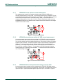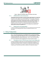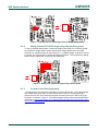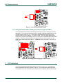
1
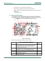
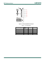
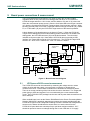
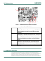
UM10855 LPCXpresso54102 Rev. 1.0 — 4th November 2014 Document information Info Content Keywords LPCXpresso54102, LPC54100 Abstract LPCXpresso54102 User Manual User manual UM10855 NXP Semiconductors LPCXpresso board for LPC54100 family of MCUs Revision history Rev Date Description 1.0 OM13077 User Manual release <20141105> Contact information For more information, please visit: http://www.nxp.com For sales office addresses, please send an email to: [email protected] UM10855_OM1377.docm User manual All information provided in this document is subject to legal disclaimers. Rev. 1.0 — 4th November 2014 © NXP B.V. 2014. All rights reserved. 2 of 19 UM10855 NXP Semiconductors LPCXpresso board for LPC54100 family of MCUs 1. Introduction The LPCXpresso™ family of boards provides a powerful and flexible development system for NXP's Cortex®-M family of MCUs. They can be used with a wide range of development tools, including the NXP’s LPCXpresso IDE. The LPCXpresso54102 board has been developed by NXP to enable evaluation of and prototyping with the LPC54100 family of MCUs, and is based on the LPC54102J512BD64 version of the MCU. This document describes the LPC54102 LPCXpresso LQFP board hardware. The following aspects of interfacing to the board are covered by this guide: Main board features Setup for use with development tools Supporting software drivers Board interface connector pin out Jumper settings Powering the board Mechanical drawing 2. Feature summary The LPCXpresso54102 board includes the following features: UM10855_OM1377.docm User manual On-board, high-speed USB based, Link2 debug probe with ARM’s CMSIS-DAP and LPCXpresso IDE Redlink protocol options Link2 probe can be used with on-board LPC54102 or external target Support for external debug probes Tri-color LED Target Reset, ISP and WAKE buttons Expansion options based on Arduino UNO and PMod™, plus additional expansion port pins All information provided in this document is subject to legal disclaimers. Rev. 1.0 — 4th November 2014 © NXP B.V. 2014. All rights reserved. 3 of 19 UM10855 NXP Semiconductors LPCXpresso board for LPC54100 family of MCUs On-board 1.8/3.3V or external power supply options Built-in power consumption and supply voltage measurement UART, I C and SPI port bridging from LPC54102 target to USB via the on-board debug probe FTDI UART connector 2 2.1 Board layout and settings This section provides a quick reference guide to the main board components, configurable items, visual indicators and expansion connectors. The layout of the components on the LPCXpresso54102 board is shown in Figure 1 below: P1 SW1 SW2 D2 P2 JP3 JP4 J1 U12 J2 JP1 J3 JP2 J4 P3 D1 JP5 TP1 J5 J6 SW3 U8 JP7 JP6 D3 D4 JP8 J7 J8 Figure 1 Board Layout The function of each identified component is listed in Table 1. Designator D1 D2 D3 D4 J1, J2, J7, J8 UM10855_OM1377.docm User manual Table 1 - Board interface components Description Link2 LPC43xx BOOT0_LED indicator. Reflects the state of LPC43xx Link2 MCU P1_1. When the boot process fails, D1 will toggle at a 1 Hz rate for 60 seconds. After 60 seconds, the LPC43xx is reset. Tri-color LED – Driven by Target LPC54102 MCU. JP6 must be shunted for +3.3V to be applied to D2 anode. The default shunt for JP6 is a 0Ω resistor installed at JS17. Target LPC54102 Power LED. Target LPC54102 Reset LED – LED is on anytime the Target RESETn is pulled low. Expansion connectors, including Arduino Uno rev3 compatible connectivity. All information provided in this document is subject to legal disclaimers. Rev. 1.0 — 4th November 2014 Reference section 7 7 7 7 8 © NXP B.V. 2014. All rights reserved. 4 of 19 UM10855 NXP Semiconductors LPCXpresso board for LPC54100 family of MCUs Designator Description J4 LPC54102 Target Power input. Connect this micro USB Btype connector to a +5V power source when it is desired to power only the LPC54102 Target, and leave the on-board Link2 debug probe unpowered. This is useful when an external debug probe is used to debug the LPC54102 Target. 2 PMod™ (SPI / I C) Bridge connector. An external Application Processor (AP) or PMod™ peripheral may be connected to the LPC54102 Target MCU SPI0 and I2C2 via this connector. FTDI serial header. In addition to provide a serial output from LPC54102, the Target side of the board can be powered from the FTDI header. The LPC54102 supports serial ISP boot from the FTDI header. Link2 micro USB B-type connector. Powers both the Link2 side of the board and LPC54102 Target side of the board. Power the board from this connector when using the onboard debug probe to debug the LPC54102 Target MCU. LPC54102 Target SWD disable – 2-position jumper pins. 1) Jumper open (default) the LPC54102 Target SWD interface enabled. Normal operating mode where the Target SWD is connected to either the on-board Link2 debug probe or an external debug probe. 2) Jumper shunted, the LPC54102 Target SWD interface is disabled. Use this setting only when the on-board Link2 debug probe is used to debug an off-board Target MCU. SWD VREF power selection – 3 position jumper pins. 1) Jumper 1 – 2 (default) when on-board LPC54102 Target is connected to either the on-board Link2 debug probe or an external debug probe. 2) Jumper 2 – 3 when on-board Link2 debug probe is used to debug an off-board Target MCU. An alternate value voltage sense resistor may be installed across JP3 terminals. By default JP3 is shunted by a 0Ω resistor installed at JS5. Remove the shunt at JS5 to use an alternate voltage sense resistor. A current meter may be installed across JP4 terminals to measure the LPC54102 current consumption. By default JP4 is shunted by a 0Ω resistor installed at JS6. Remove the shunt at JS6 to measure current at JP4. Link2 (LPC43xx) force DFU boot – 2 position jumper pins. 1) Jumper open (default) for Link2 to follow the normal boot sequence. The Link2 will boot from internal flash if image is found there. With the internal flash erased the Link2 normal boot sequence will fall through to DFU boot. 2) Jumper shunted to force the Link2 to DFU boot mode. Use this setting to reprogram the Link2 internal flash with a new image or to use the LPCXpresso IDE with Redlink protocol. J3 J5 J6 JP1 JP2 JP3 JP4 JP5 UM10855_OM1377.docm User manual All information provided in this document is subject to legal disclaimers. Rev. 1.0 — 4th November 2014 Reference section 5 8 4.1 5 6 5 5.1.2 5.1.3 6.1.3 © NXP B.V. 2014. All rights reserved. 5 of 19 UM10855 NXP Semiconductors LPCXpresso board for LPC54100 family of MCUs Designator Description JP6 Tri-color LED anode voltage enable – 2-position jumper pins. 1) By default JP6 is shunted by a 0Ω resistor installed at JS17. 2) To disable +3.3V to the tri-color led common anode, remove the 0Ω resistor installed at JS17. LPC54102 VDD voltage select – 3-position jumper 1) Jumper 1 – 2 to select +1.8V LPC54102 VDD. 2) Jumper 2 – 3 (default) to select +3.3V LPC54102 VDD. LPC54102 ADC VREFP, VREFN off-board access – 3 position header. Can be used to apply different reference voltages for the LPC54102 ADC. 10-pin SWD connector – The SWD connector is used to debug the LPC54102 Target from an external debug probe. The same SWD connector can also be used to connect the on-board Link2 debug probe to an off-board Target MCU (for this JP1 must be shunted). LPC54102 VDD current monitor Vsense measurement. The Vsense can be measured with a volt meter. Pin 1 (square pad) is positive and pin 2 is negative. LPC54102 current is calculated by dividing the measured voltage at P2 by the Vsense resistance value of 8.2Ω. +5V External Voltage Input allows for powering the LPC54102 Target side of the board from a bench-top power supply. Pin 1 (square pad) is +5V and pin 2 is gnd. LPC54102 Target WAKEUP pushbutton. When pressed the WAKEUP switch will drive LPC54102 P0_24 to a low level. LPC54102 ISP Bootload enable pushbutton. This switch drives LPC54102 P0_31 low. Holding SW2 pressed while powering up or reseting and the LPC54102 Target will enter ISP mode. LPC54102 Target Reset pushbutton. Ground terminal test point. Link2 MCU LPC54102 Target LQFP64 MCU JP7 JP8 P1 P2 P3 SW1 SW2 SW3 TP1 U8 U12 Reference section 5.1 and 7 5 LPC54100 User Manual 6 5.1.1 5 9.3 9.2 9.1 n/a n/a n/a 3. Getting Started By default, the LPCXpresso54102 is configured to use the on-board debug probe (Link2) to debug the on-board target (LPC54102), using the CMSIS-DAP debug protocol preprogrammed into the Link2 Flash memory. The LPCXpresso IDE (available for free download at http://www.lpcware.com/lpcxpresso/home) or development tools that support the CMSIS-DAP protocol can be used in the default configuration. Check with your toolchain vendor for availability of specific device support packs for the LPC54100 family of devices. (Note that the LPCXpresso IDE can also be used with redlink protocol by booting the Link2 in DFU mode, by installing a jumper on JP5.) Installation steps for use with LPCXpresso IDE (steps 1 and 2 apply to all use tool chains): UM10855_OM1377.docm User manual All information provided in this document is subject to legal disclaimers. Rev. 1.0 — 4th November 2014 © NXP B.V. 2014. All rights reserved. 6 of 19 UM10855 NXP Semiconductors LPCXpresso board for LPC54100 family of MCUs 1) Download and install the LPCXpresso Link2 USB driver package installer from http://www.lpcware.com/content/nxpfile/lpcxpresso-link2-usb-driver-package (only required if using Windows). 2) When the installer has completed, connect the LPCXpresso54102 board to the USB port of your host computer, connecting a micro USB cable to connector J6 (“Link”). 3) Allow about 30 seconds for the LPCXpresso54102 devices to enumerate. There will be four devices: CMSIS-DAP, LPC-LinkII, LPC-SIO Port, and VCOM. 4) Download the LPCOpen examples & drivers from http://www.lpcware.com/content/nxpfile/lpcopen-software-development-platformlpc5410x-packages, selecting the version for the toolchain you are using; project files for LPCXpresso IDE, Keil and IAR tools are available. 5) Start the LPCXpresso IDE and import the LPCOpen zip file by clicking Import project(s) in the “Start here panel.” 6) The simplest example is periph_blinky, which will blink the tricolor LED on the LPCXpresso54102. Click on the periph_blinky in the “Project Explorer” panel, then click Debug ‘periph_blinky’ in the “Start here” panel. This will build the project and then launch the debug session. The LPCXpresso IDE can also be used with the Link2 configured for DFU boot (JP5 fitted); in this configuration the LPCXpresso IDE will load the Redlink protocol driver into the Link2. Note that if the jumper setting of JP5 is changed with the board powered then the USB connection must be removed and reconnected to J6 in order to force the Link2 to reset and enter DFU boot mode. Redlink protocol is required for multicore debug using the LPCXpresso IDE. 4. LPC54102 Serial ports By default the LPC54102 UART0 is connected to the FTDI header at J5. This can be used for ISP booting or sending debug messages out to a host computer via a suitable cable. The LPC54102 UART0 can also be connected through a virtual communication port (VCOM) UART bridge Link2 function to a host computer connected to the J6 USB Link2. The factory default CMSIS-DAP Link2 image includes UART bridge functionality (VCOM support), and this firmware is also available with the Link Configuration Tool (LCT), available at http://www.lpcware.com/. When running this firmware the default source of data to the LPC54102 RXD is the FTDI header. Once the Link2 receives any data via the VCOM port of a host computer it will set P2_2 low to select the Link2 UART0 data to the LPC54102. In order to reset this so the FTDI connection can be used it is necessary to power cycle the board. 4.1 J5 FTDI header The FTDI header J5 mates with FTDI cable TTL-232R-3V3. J5 interfaces the LPC54102 UART0 to a Host PC virtual serial port. The J5 location is shown in Figure 2. The pin out and a description of the signals at J5 are listed in Table 2. By default there may be no header installed at J5. UM10855_OM1377.docm User manual All information provided in this document is subject to legal disclaimers. Rev. 1.0 — 4th November 2014 © NXP B.V. 2014. All rights reserved. 7 of 19 UM10855 NXP Semiconductors LPCXpresso board for LPC54100 family of MCUs 1 2 3 4 5 6 . Figure 2 – FTDI (J5) LPC54102 serial port Table 2 – J5 FTDI interface LPC54102 Signal GND No connect Board +5V UART0_RXD UART0_TXD No connect UM10855_OM1377.docm User manual FTDI Signal GND CTS 5V TXD RXD RTS Pin # 1 2 3 4 5 6 All information provided in this document is subject to legal disclaimers. Rev. 1.0 — 4th November 2014 Direction From host To host © NXP B.V. 2014. All rights reserved. 8 of 19 UM10855 NXP Semiconductors LPCXpresso board for LPC54100 family of MCUs 5. Board power connections & measurement The LPCXpresso54102 board requires +5V input to power the on-board voltage regulators which in turn power the Link2 debug probe and other +3.3V circuits, the LPC54102 target and other +1.8V circuits, and the Arduino +5V and +3.3V power rails. When the main external power source is from the Link2 side USB micro B-type connector (J6), both the Link side and LPC54102 Target sections of the board are powered. When the main external power is from the Target side USB micro B-type connector (J4), header P3, or FTDI header (J5) only the LPC54102 Target section of the board is powered. A block diagram of the board power tree is shown in Figure 3. When the LPC54102 Target is to be debugged from an external debug probe, instead of the on-board Link2 debug probe, the Link USB connector (J6) must be disconnected. The circle with I indicates a current monitor chip. Note that the LPC54102 does not provide a USB interface, the Target USB connector J4 is for power only. The LPC54102 Target VDD selection of 1.8V or 3.3V is made at JP7, with 3.3V set as the default. Target section of board FTDI Header (J5) Target External +5V Micro-B (J4) Target +1.8V LDO (U17) LPC54102 Target +3.3V LDO (U18) +5V Arduino connector I VDD_NIOBE Tri-color LED P3 External_VIN Bridge SPI / I2C JP7 +3.3V +5V Link USB Micro-B (J6) Vbus Link +2.5V LDO (U19) Link section of board +2.5V SWD Dual Supply Voltage buffer VDD_NIOBE Figure 3 - Board Power block diagram 5.1 LPCXpresso54102 current measurement The LPC54102 current can be measured by measuring the voltage across a sense resistor in series with the supply, a current meter or using the on board current measurement circuit. Each of these methods will be described in subsections below. There is no current monitoring of the Link section circuits on the board. The Target side power going to LEDs and support ICs is not monitored by the current measurement circuit. The LPC54102 LQFP package has the core and IO power both sourced from the same VDD pins. When a shield board, such as the Sensor Shield Board in the Sensor Processing/Motion Solution (OM13078) is attached, attempting to measure the lowest possible power the LPC54102 IO pins must be configured according to how the software has configured the sensors on the Sensor shield board to ensure there is no extra current from the LPC54102 IO ports that have external pull-up or pull-down resistors enabled. JS17 should be opened to ensure no leakage through the tri-color LED and +3.3V supply. UM10855_OM1377.docm User manual All information provided in this document is subject to legal disclaimers. Rev. 1.0 — 4th November 2014 © NXP B.V. 2014. All rights reserved. 9 of 19 UM10855 NXP Semiconductors LPCXpresso board for LPC54100 family of MCUs 5.1.1 LPC54102 Vsense resistor current measurement + The voltage across a series 8.2Ω resistor with the target LPC54102 VDD can be manually measured at P2 on the PCB. The voltmeter positive probe is applied to P2 pin 1 (square pad) and negative probe to P2 pin 2, see Figure 4. Use Ohm’s law to calculate the current (LPC54102 current = measured voltage / 8.2Ω). As an example if the measured voltage is 20mV, then 20e-3 / 8.2Ω = 2.44mA. Note that the input current to the MAX9634 used in the on-board current measurement will be included in the voltage measured across this resistor. V Figure 4 - Vsense measurement 5.1.2 LPC54102 external sense resistor for VDD current measurement + It is not required to use an external sense resistor for LPC54102 current measurement. To measure LPC54102 VDD current of less than 4 uA an external resistor is required. The external resistor should be installed between the JP3 terminals, and the 0Ω resistor at JS5 must be removed. The external resistor will be in series with the on-board 8.2Ω (R18), so the external resistor value is added to 8.2Ω to get the combined Vsense resistance. The voltage measurement is made across the total series resistance from P2-1 to JP3-2, as shown in Figure 5. To calculate the LPC54102 current divide the voltage read by the combined sense resistance. To restore the JS5 short around JP3, use a solder bridge across JS5. V Ext resistor remove Figure 5 - External vSense resistor 5.1.3 LPC54102 VDD current measurement using a current meter A current meter may be inserted at JP4 to measure the LPC54102 VDD input current. The 0Ω resistor at JS6 must be removed and the current meter connected at the positive input at JP4 pin 1 (square pad) and negative input at JP2 pin 2, as shown in Figure 6. UM10855_OM1377.docm User manual All information provided in this document is subject to legal disclaimers. Rev. 1.0 — 4th November 2014 © NXP B.V. 2014. All rights reserved. 10 of 19 UM10855 NXP Semiconductors remove + LPCXpresso board for LPC54100 family of MCUs - I Figure 6 - Measuring LPC54102 VDD current with current meter 5.1.4 LPC54102 VDD current measurement The LPCXpresso54102 board has an on-board current measurement circuit consisting of a MAX9634T (U5) current monitor chip and a 12-bit ADC (ADC122S021, U11) with a 12bit sample at 50k to 200ksps. The on-board MAX9634T current monitor measures the voltage across the LPC54102 VDD 8.2Ω vsense resistor. The MAX9634 multiplies the sense voltage by 25 to provide a voltage range suitable for the ADC to measure. A 2input analog mux selects between the LPC54102 current monitor and the output on a MAX9634T current monitor chip on an expansion board (with compatible current measurement circuit on-board). The current measurement circuit is controlled by the Link2 processor and is not user programmable. For available power measurement utilities please visit http://www.lpcware.com. 5.1.5 Shield board current measurement To use the on-board current measurement circuitry, any expansion board must match the functionality of the LPCXpresso54102. Refer to the board schematics for more information. 6. Debug Configurations The LPCXpresso54102 LQFP board has a built-in debug probe using the Link LPC43xx MCU. The LPC54102 target MCU can be debugged by the on-board Link debugging probe, or from an external debug probe installed at P1. On-board jumpers JP1 and JP2 must be correctly positioned for each mode. The on-board Link debug probe is capable of debugging target MCU’s with a VDDIO range of 1.6V to 3.6V. Use JP7 to set the LPC54102 chip VDD to the desired voltage level (+1.8V or +3.3V). Check the sections below for the appropriate jumper settings and how to properly power the board. 6.1.1 Debugging on-board LPC54102 target using on-board debug probe To use the on-board Link debug probe, the LPCXpresso54102 board must be powered from the Link2 USB connector J6, and jumper JP2 must be fitted in position pin 1 - 2 (Local Target), as shown in Figure 7. Jumper JP1 must be open to enable the target LPC54102. Connecting the micro USB J6 to a host computer will power the Link and Target sections of the board and provide the USB link to the debug tool software. UM10855_OM1377.docm User manual All information provided in this document is subject to legal disclaimers. Rev. 1.0 — 4th November 2014 © NXP B.V. 2014. All rights reserved. 11 of 19 UM10855 NXP Semiconductors LPCXpresso board for LPC54100 family of MCUs Figure 7 – Debug local LPC54102 target from on-board debug probe 6.1.2 Debug on-board LPC54102 target using external debug probe To use an external debug probe, connect the probe to the SWD (P1) connector, power the LPC54102 Target section of the board from the Target power only micro USB connector J4, and fit a jumper to JP2 across pin 1 - 2 (Local Target), as shown in Figure 8. Jumper JP1 must be open to enable the target LPC54102. The on-board Link debug probe must be unpowered, by leaving J6 unconnected. Figure 8 - Debug local LPC54102 target using external probe 6.1.3 On-board Link2 flash programing To program the Link2 Flash the Link2 MCU must be in DFU mode. If the Link2 already has a valid image in the flash, you will need to force it into DFU mode by placing a jumper shunt on JP5, then power the board by connecting the micro USB J6 to a host computer, as shown in Figure 9. Link2 MCU programming is performed using DFUSec tool found on http://www.lpcware.com/content/project/dfu-download-programming-utilityand-security-lpcdfusec-tool. Instructions for using the tool are located at the same web page. UM10855_OM1377.docm User manual All information provided in this document is subject to legal disclaimers. Rev. 1.0 — 4th November 2014 © NXP B.V. 2014. All rights reserved. 12 of 19 UM10855 NXP Semiconductors LPCXpresso board for LPC54100 family of MCUs Figure 9 - Link LPC43xx MCU DFU mode 6.2 Using on-board Link2 to debug an off-board target LPC MCU The LPCXpresso54102 board’s Link2 debug probe may be used to debug an off-board target MCU. The on-board Link debug probe is capable of debugging target MCU’s with a VDDIO range of 1.6V to 3.6V. To keep the on-board target LPC54102 MCU from interfering with the SWD interface, JP1 must be fitted. The Link2 debug probe SWD is connected by a ribbon cable between the P1 connector to the off-board target MCU SWD interface. Power the LPCXpresso54102 board from the Link USB connector J6, and jumper JP2 must be fitted across pins 2 - 3 (External Target), as shown in, as shown in Figure 10. Figure 10 - Link debug probe debugging off-board target 7. LED indicators The LPCXpresso54102 board LED locations are shown in Figure 11. A description of each on-board LED indicator is shown is Table 3. The current through the LEDs does not contribute to current monitored by the current monitor methods shown in this manual. UM10855_OM1377.docm User manual All information provided in this document is subject to legal disclaimers. Rev. 1.0 — 4th November 2014 © NXP B.V. 2014. All rights reserved. 13 of 19 UM10855 NXP Semiconductors LPCXpresso board for LPC54100 family of MCUs D1 D2 D3 D4 Figure 11 – LPCXpresso54102 LQFP board LED Indicators Table 3 - Board LED indicators Description Link2 Debug Probe BOOT0_LED indicator. Driven by P1_1 of the LPC43xx. This LED will remain unlit when using the CMSIS-DAP firmware image (normal boot). When using LPCXpresso with the board configured for DFU boot, this LED will flash during debug operations. Tri-color LED – Driven by Target LPC54102 MCU. The red led is driven by P0_29. The green led is driven by P0_30. The blue led is driven by P0_31. LEDs are on when the LPC54102 port is output low. To light any of the tri-color leds, JP6 must have a shunt between pins 1 – 2. By default the 0Ω resistor at JS17 provides the shunt for JP6. To measure the lowest possible current from LPC54102 remove the 0Ω resistor at JS17 (remove +3.3V from led common anode). Target LPC54102 power LED. This LED is on any time power is applied to the Target LPC54102 MCU. LED will have a brighter intensity when the LPC54102 is powered from +3.3V than when powered by +1.8V. Target Reset LED. This LED is on anytime the Target RESETn is pulled low. LED reference D1 D2 D3 D4 8. Expansion connectors The LPCXpresso54102 board includes four expansion connectors plus a PMod™ compatible connector (J3). The expansion connectors (J1, J2, J7 and J8) incorporate an Arduino Uno revision 3 footprint in their inner rows. Not all connector locations are populated on the expansion connectors since the LPC54102 does not have enough I/O UM10855_OM1377.docm User manual All information provided in this document is subject to legal disclaimers. Rev. 1.0 — 4th November 2014 © NXP B.V. 2014. All rights reserved. 14 of 19 UM10855 NXP Semiconductors LPCXpresso board for LPC54100 family of MCUs to utilize all of the available connections (additional pin locations are provided for compatibility with future LPCXpresso boards.) Table 4 Expansion Connectors Reference J1 J2 J3 J7 J8 The odd number pins are compatible with Arduino Uno rev3 Digital 15:8, AREF, SDA & SCL connector. The even numbered pins are used for external access and expansion of LPC54102 signals not used by the Arduino Uno rev3 compatible interface. The odd numbered pins 1 – 13 are compatible with Arduino Uno rev3 Digital 7:0 connector. The even numbered pins, and odd numbered pins 17 and 19, are used for external access and expansion of LPC54102 signals not used by the Arduino Uno rev3 compatible interface. PMod™ connector. Connected to the LPC54102 Target MCU SPI0 and I2C2. The even numbered pins 6 – 20 are compatible with Arduino Uno rev3 Power connector. The odd numbered pins, and even numbered pins 2 and 4 are used. The even numbered pins 2 – 12 are compatible with Arduino Uno rev3 Analog connector. The odd numbered pins are used for external access and expansion of LPC54102 signals not used by the Arduino Uno rev3 compatible interface. 9. Buttons The LPCXpresso54102 board has 3 push buttons available to control the operation of the LPC54102 (target) MCU. Their functions are as described below. 9.1 Reset This button is used to reset the LPC54102. 9.2 ISP This button connects to the LPC54102 P0_31 pin and may be used to force the LPC54102 into ISP boot mode. This can be useful when the LPC54102 flash has been programmed with code that disables the SWD debug pins or changes timing settings such that the debug probe has problems communicating with it. To force ISP boot, hold the ISP button down while pressing and releasing the reset button. The ISP button can also be used to trigger an interrupt by configuring the P0_31 pin and associated interrupt controls within your application code. 9.3 WAKEUP Depressing this button triggers a wake interrupt by pulling down the WAKEUP input (P0_24) of the LPC54102. UM10855_OM1377.docm User manual All information provided in this document is subject to legal disclaimers. Rev. 1.0 — 4th November 2014 © NXP B.V. 2014. All rights reserved. 15 of 19 UM10855 NXP Semiconductors LPCXpresso board for LPC54100 family of MCUs 10. Legal information provide appropriate design and operating safeguards to minimize the risks associated with their applications and products. 10.1 Disclaimers Limited warranty and liability — Information in this document is believed to be accurate and reliable. However, NXP Semiconductors does not give any representations or warranties, expressed or implied, as to the accuracy or completeness of such information and shall have no liability for the consequences of use of such information. In no event shall NXP Semiconductors be liable for any indirect, incidental, punitive, special or consequential damages (including - without limitation lost profits, lost savings, business interruption, costs related to the removal or replacement of any products or rework charges) whether or not such damages are based on tort (including negligence), warranty, breach of contract or any other legal theory. Notwithstanding any damages that customer might incur for any reason whatsoever, NXP Semiconductors’ aggregate and cumulative liability towards customer for the products described herein shall be limited in accordance with the Terms and conditions of commercial sale of NXP Semiconductors. Right to make changes — NXP Semiconductors reserves the right to make changes to information published in this document, including without limitation specifications and product descriptions, at any time and without notice. This document supersedes and replaces all information supplied prior to the publication hereof. Suitability for use — NXP Semiconductors products are not designed, authorized or warranted to be suitable for use in life support, life-critical or safety-critical systems or equipment, nor in applications where failure or malfunction of an NXP Semiconductors product can reasonably be expected to result in personal injury, death or severe property or environmental damage. NXP Semiconductors accepts no liability for inclusion and/or use of NXP Semiconductors products in such equipment or applications and therefore such inclusion and/or use is at the customer’s own risk. Applications — Applications that are described herein for any of these products are for illustrative purposes only. NXP Semiconductors makes no representation or warranty that such applications will be suitable for the specified use without further testing or modification. Customers are responsible for the design and operation of their applications and products using NXP Semiconductors products, and NXP Semiconductors accepts no liability for any assistance with applications or customer product design. It is customer’s sole responsibility to determine whether the NXP Semiconductors product is suitable and fit for the customer’s applications and products planned, as well as for the planned application and use of customer’s third party customer(s). Customers should UM10855_OM1377.docm User manual NXP Semiconductors does not accept any liability related to any default, damage, costs or problem which is based on any weakness or default in the customer’s applications or products, or the application or use by customer’s third party customer(s). Customer is responsible for doing all necessary testing for the customer’s applications and products using NXP Semiconductors products in order to avoid a default of the applications and the products or of the application or use by customer’s third party customer(s). NXP does not accept any liability in this respect. Evaluation products — This product is provided on an “as is” and “with all faults” basis for evaluation purposes only. NXP Semiconductors, its affiliates and their suppliers expressly disclaim all warranties, whether express, implied or statutory, including but not limited to the implied warranties of noninfringement, merchantability and fitness for a particular purpose. The entire risk as to the quality, or arising out of the use or performance, of this product remains with customer. In no event shall NXP Semiconductors, its affiliates or their suppliers be liable to customer for any special, indirect, consequential, punitive or incidental damages (including without limitation damages for loss of business, business interruption, loss of use, loss of data or information, and the like) arising out the use of or inability to use the product, whether or not based on tort (including negligence), strict liability, breach of contract, breach of warranty or any other theory, even if advised of the possibility of such damages. Notwithstanding any damages that customer might incur for any reason whatsoever (including without limitation, all damages referenced above and all direct or general damages), the entire liability of NXP Semiconductors, its affiliates and their suppliers and customer’s exclusive remedy for all of the foregoing shall be limited to actual damages incurred by customer based on reasonable reliance up to the greater of the amount actually paid by customer for the product or five dollars (US$5.00). The foregoing limitations, exclusions and disclaimers shall apply to the maximum extent permitted by applicable law, even if any remedy fails of its essential purpose. 10.2 Trademarks Notice: All referenced brands, product names, service names and trademarks are property of their respective owners. LPCXpresso — is a trademark of NXP B.V. All information provided in this document is subject to legal disclaimers. Rev. 1.0 — 4th November 2014 © NXP B.V. 2014. All rights reserved. 16 of 19 UM10855 NXP Semiconductors LPCXpresso board for LPC54100 family of MCUs 11. List of figures Figure 1 Board Layout ........................................................ 4 Figure 2 – FTDI (J5) LPC54102 serial port ......................... 8 Figure 3 - Board Power block diagram................................ 9 Figure 4 - Vsense measurement ....................................... 10 Figure 5 - External vSense resistor ................................... 10 Figure 6 - Measuring LPC54102 VDD current with current meter............................................................... 11 Figure 7 – Debug local LPC54102 target from on-board debug probe .................................................... 12 Figure 8 - Debug local LPC54102 target using external probe ............................................................... 12 Figure 9 - Link LPC43xx MCU DFU mode ........................ 13 Figure 10 - Link debug probe debugging off-board target . 13 Figure 11 – LPCXpresso54102 LQFP board LED Indicators ........................................................................ 14 UM10855_OM1377.docm User manual All information provided in this document is subject to legal disclaimers. Rev. 1.0 — 4th November 2014 © NXP B.V. 2014. All rights reserved. 17 of 19 UM10855 NXP Semiconductors LPCXpresso board for LPC54100 family of MCUs 12. List of tables Table 1 - Board interface components ................................ 4 Table 2 – J5 FTDI interface ................................................ 8 Table 3 - Board LED indicators ......................................... 14 Table 4 Expansion Connectors ......................................... 15 UM10855_OM1377.docm User manual All information provided in this document is subject to legal disclaimers. Rev. 1.0 — 4th November 2014 © NXP B.V. 2014. All rights reserved. 18 of 19 UM10855 NXP Semiconductors LPCXpresso board for LPC54100 family of MCUs 13. Contents 1. 2. 2.1 3. 4. 4.1 5. 5.1 5.1.1 5.1.2 5.1.3 5.1.4 5.1.5 6. 6.1.1 6.1.2 6.1.3 6.2 7. 8. 9. 9.1 9.2 9.3 10. 10.1 10.2 11. 12. 13. Introduction ......................................................... 3 Feature summary ................................................ 3 Board layout and settings ................................... 4 Getting Started .................................................... 6 LPC54102 Serial ports ........................................ 7 J5 FTDI header .................................................. 7 Board power connections & measurement....... 9 LPCXpresso54102 current measurement .......... 9 LPC54102 Vsense resistor current measurement ......................................................................... 10 LPC54102 external sense resistor for VDD current measurement ....................................... 10 LPC54102 VDD current measurement using a current meter .................................................... 10 LPC54102 VDD current measurement ............. 11 Shield board current measurement .................. 11 Debug Configurations ....................................... 11 Debugging on-board LPC54102 target using onboard debug probe ........................................... 11 Debug on-board LPC54102 target using external debug probe ..................................................... 12 On-board Link2 flash programing ..................... 12 Using on-board Link2 to debug an off-board target LPC MCU ............................................... 13 LED indicators ................................................... 13 Expansion connectors ...................................... 14 Buttons ............................................................... 15 Reset................................................................ 15 ISP ................................................................... 15 WAKEUP.......................................................... 15 Legal information .............................................. 16 Disclaimers....................................................... 16 Trademarks ...................................................... 16 List of figures..................................................... 17 List of tables ...................................................... 18 Contents ............................................................. 19 Please be aware that important notices concerning this document and the product(s) described herein, have been included in the section 'Legal information'. © NXP B.V. 2014. All rights reserved. For more information, please visit: http://www.nxp.com For sales office addresses, please send an email to: [email protected] Date of release: 4th November 2014 Document identifier: UM10855_OM1377.docm