1
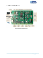
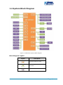
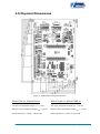
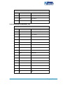
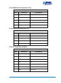
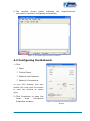
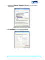
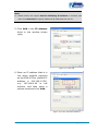
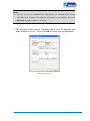
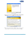
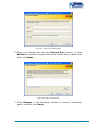
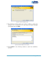
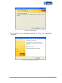
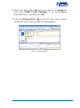
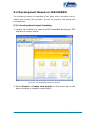
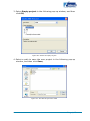
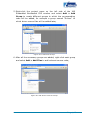
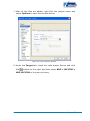
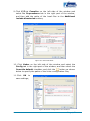
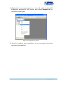
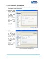
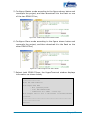
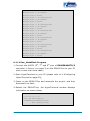
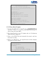
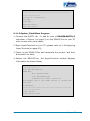
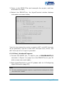
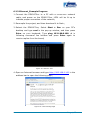
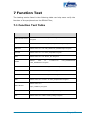
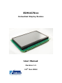
EDM1070xx Embedded Display Module User Manual Version 1.1 13th Jan 2014 Copyright Statement: Unless otherwise specified, the EDM1070xx series mentioned in this document includes but is not limited to the following products: EDM1070A-01, EDM1070AR-01, EDM1070B-01, and EDM1070BR-01. EDM1070xx and its related intellectual property are owned by Shenzhen Embest Technology Co., Ltd. Shenzhen Embest Technology has the copyright of this document and reserves all rights. Any part of the document should not be modified, distributed or duplicated in any approach and form without prior written permission issued by Embest Technology Co., Ltd. Revision History: Version Date Description 1.0 04/10/2013 Original Version 1.1 13/01/2014 Localisation Table of Contents 1 Product Overview .............................................................. 1 1.1 Introduction ....................................................................1 1.2 Kit Contents ....................................................................2 1.3 Board Interfaces ..............................................................3 1.4 System Block Diagram .....................................................4 1.5 Physical Dimensions .........................................................5 2 Hardware Features ............................................................ 6 2.1 Processor .......................................................................6 2.2 On-Board Memories .........................................................7 2.3 Communication Interfaces ................................................7 2.4 Other .............................................................................8 2.5 Electrical Features ...........................................................8 3 Hardware Details ............................................................... 9 3.1 CPU Introduction .............................................................9 3.2 Interface Introduction ......................................................9 3.2.1 Power Jack (J2) ......................................................................... 9 3.2.2 Ethernet Interface (J3) ............................................................. 10 3.2.3 USB Device Interface (J4) ......................................................... 11 3.2.4 USB Host Interface (J5) ............................................................ 11 3.2.5 TF Card Slot (CON1) ................................................................ 11 3.2.6 LCD Interface (CON2) .............................................................. 12 3.2.7 Touchscreen Interface (CON3/CON15) ........................................ 14 3.2.8 UART and RS485 Interfaces (CON4) ........................................... 15 3.2.9 UART3 and CAN Interfaces (CON5) ............................................ 15 3.2.10 JTAG Interface (CON6) ........................................................... 16 3.2.11 Isolated GPIO Interface (CON7/CON14) .................................... 17 3.2.12 SPIFI Interface (CON10) ......................................................... 17 3.2.13 SGPIO Interface (CON11) ....................................................... 18 3.2.14 ADC/DAC/GPIO Interfaces (CON12) ......................................... 18 3.2.15 I2S/I2C/GPIO Interfaces (CON13) ............................................ 19 3.2.16 Camera Interface (CON16) ...................................................... 20 4 Preparations .................................................................... 22 4.1 Configuring HyperTerminal ............................................. 22 4.2 Configuring the Network ................................................. 24 4.3 Installing the Keil MDK ................................................... 28 4.4 Installing IAR EWARM .................................................... 33 5 Software Development Process ....................................... 38 5.1 Development Based on the Keil MDK ................................ 38 5.1.1 Creating and Compiling a New Project ........................................ 38 5.1.2 Programming and Debugging .................................................... 43 5.2 Development Based on IAR EWARM ................................. 47 5.2.1 Creating New Project Compiling ................................................. 47 5.2.2 Programming and Debugging .................................................... 53 6 Example Programs .......................................................... 55 6.1 Basic Example Programs for Peripherals ........................... 55 6.1.2 LCD_Touch Program................................................................. 58 6.1.3 Lcd_Demo Program .................................................................. 59 6.1.4 USB_DEV/Usb_MassStorage Program ......................................... 59 6.1.5 USB_DEV/Usb_Cdc Program...................................................... 60 6.1.6 USB_HOST/Usb_MassStorage Program ....................................... 61 6.1.7 Emac_EasyWeb Program .......................................................... 63 6.1.8 Adc_Polling Program ................................................................ 64 6.1.9 Atimer_Wic Program ................................................................ 65 6.1.10 Ccan_SimpleTxRx Program ..................................................... 66 6.1.11 Emc_NandFlash Program ........................................................ 68 6.1.12 Emc_Sdram Program .............................................................. 69 6.1.13 Gpdma_Flash2Ram Program ................................................... 70 6.1.14 Gpio_LedBlinky Program ......................................................... 71 6.1.15 I2C_EEPROM Program ............................................................ 71 6.1.16 Rtc_Calendar Program ............................................................ 72 6.1.17 Sdio_FatFs Program ............................................................... 73 6.1.18 Wdt_Interrput Program ........................................................... 74 6.1.19 Uart_Autoband Program ......................................................... 75 6.1.20 Uart_Rs485Master& Uart_Rs485Slave Program .......................... 76 6.1.21 Pwr_DeepSleep Program ......................................................... 78 6.1.22 Mbx_Demo Program ............................................................... 79 6.2 Application Programs ..................................................... 81 6.2.1 Camera_Example Program ........................................................ 81 6.2.2 emWin518_Example Program .................................................... 82 6.2.3 Ethernet_Example Program ....................................................... 83 6.2.4 uCOS_II&emWin518_Example Program ...................................... 84 6.2.5 uCOS_II_Example Program ....................................................... 84 7 Function Test ................................................................... 85 7.1 Function Test Table ........................................................ 85 Appendix 1: ESD Precautions & Proper Handling Procedures86 Appendix 2: Technical support & Warranty .......................... 1 2.1 Technical support service ..................................................1 2.2 Maintenance service clause ...............................................2 2.3 Basic guidelines for protection and maintenance of LCDs ......3 2.4 Value Added Services .......................................................4 1 Product Overview 1.1 Introduction The EDM1070xx is an embedded display module designed by Embest Technology and built on the LPC4357FET256 (a NXP 32-bit ARM CortexM4/M0 dual-core MCU) / LPC1857FET256(NXP 32-bit ARM Cortex-M3 MCU). The EDM1070xx is provided with example applications for all the on-board devices and support for real-time operating systems. It has a variety of expansion interfaces such as UART, CAN, SPI, SGPIO, I2C, GPIO and ADC/DAC to satisfy the many different application requirements of users. The EDM1070xx is suited for a wide scope of applications and can meet the requirements of many different fields including: Instrumentation, Home automation, Medical diagnosis, Motor control. Page | 1 1.2 Kit Contents EDM1070xx Board CD containing: User Manual Source code Development tools Four hexagonal screws Four hexagonal screw nuts Optional: COM1000A (SPI to serial module with 4 serial ports) DM-CAM130 (camera module with OV9655 and a 1.3MP CMOS SXGA camera sensor) Page | 2 1.3 Board Interfaces Figure 1: EDM1070xx Board Interfaces Page | 3 1.4 System Block Diagram Figure 2: EDM1070xx System Block Diagram Block Diagram Legend Legend Description Interface modules of CPU Chips or spare solder pads on the board Interfaces on the board Page | 4 1.5 Physical Dimensions Figure 3: EDM1070xx Physical Dimensions EDM1070A-01, EDM1070B-01 EDM1070AR-01, EDM1070BR-01 Top Layer Component Height Top Layer Component Height MAX Bottom Layer Component Height = 3 mm MAX = 14 mm Board Thickness =1.6mm, 4 layer PCB MAX Bottom Layer Component Height = 12 mm MAX = 14 mm Board Thickness =1.6mm, 4 layer PCB Page | 5 2 Hardware Features 2.1 Processor NXP LPC4357FET256/LPC1857FET256 Floating-point hardware unit 1024KB Flash 136 KB SRAM 16KB EEPROM LCD controller with support for 24bpp true-colour mode and a resolution of up to 1024×768 USB 2.0 high-speed Host/Device/OTG interface with on-chip PHY and support for DMA transmission USB 2.0 high-speed Host/Device interface with on-chip PHY and ULPI which supports external high-speed PHY 10/100 Mb Ethernet MAC MII/RMII interface Four-wire SPI flash interface (SPIFI) with data transfer rate of up to 40Mbps per channel Two CAN 2.0B, four UART, two I2S, two I2C, two SSP busses and one SPI bus Four 32-bit general purpose timer, two standard PWM, one motor control PWM with Quadrature encoder interface Two 10-bit ADCs operating at up to 400KHz 10-bit DAC operating at up to 400KHz Serial GPIO interface (SGPIO) 164 general-purpose I/O interfaces Two watchdog timers Page | 6 2.2 On-Board Memories 128MB NAND Flash 32MB SDRAM 2Kb EEPROM 4Mb SPI Flash (spare solder pads) 2.3 Communication Interfaces Three serial interfaces implemented with phoenix connectors UART0: 3-wire serial interface, RS232 level UART2: 3-wire serial interface, RS232 level UART3: 3-wire serial interface, RS232 level RS485 interface implemented with phoenix connectors Two CAN2.0B interfaces implemented with phoenix connectors Two USB interfaces USB2.0 Device, High-speed, 480Mbps USB2.0 Host, Full-speed, 12Mbps 10/100Mbps Ethernet interface TF card slot 20-pin standard JTAG debug interface Four input and four output I/O interfaces implemented with phoenix connectors and isolated by optocouplers 8-channel ADC interface DAC interface SPIFI interface IIC interface I2S interface High-precision RTC (no battery by default) Spare interface for external hardware watchdog Page | 7 2.4 Other 7” (800x480) TFT LCD, 16bit RGB565 mode, supporting 4-wire resistive touch-screen ISP button Buzzer 5V power output interface 2.5 Electrical Features Operating Temperature: 0 °C ~ 70 °C Storage Temperature: -40 °C ~ 85 °C Operating Humidity: 0% ~ 90% (Non-condensing) Power Supply: DC 9~24V, 150~400mA@12V Electrical Standards: CE, FCC and CCC PCB Layers: 6 Page | 8 3 Hardware Details This chapter will give you an overview of the product hardware system by introducing the CPU and interfaces used on the EDM1070xx. 3.1 CPU Introduction The EDM1070xx uses NXP’s LPC4357FET256 / LPC1857FET256 – a lowpower high- performance-price-ratio MCU based on ARM-32bit CortexM4/M0 / ARM-32bit Cortex-M3. The LPC4357FET256 is the latest processor from NXP built with asymmetric dual-core digital signal controller architecture based on the ARM Cortex-M4 and Cortex-M0 processors, which provides DSP and MCU application developers with a signal architecture and development environment. The family of the processors works at 204MHz and integrates on-chip high-speed memory and abundant peripheral interfaces. 3.2 Interface Introduction The EDM1070xx provides many different on-board interfaces such as RS232, Ethernet, USB Host/Device, TF card and LCD interfaces. This section will give you a brief introduction for each of these interfaces. 3.2.1 Power Jack (J2) Input Power Jack Pins Definitions Descriptions 1 +12V Input power jack 2 GND Grounded 3 GND Grounded Page | 9 Output Power Jack Pins Definitions Descriptions 1 +12V Output power jack 2 GND Grounded 3 GND Grounded 3.2.2 Ethernet Interface (J3) Ethernet Interface Pins Definitions Descriptions 1 TX+ TX+ output 2 TX- TX- output 3 RX+ RX+ input 4 CT CT 5 CT CT 6 RX- RX- input 7 NC NC 8 SHIELD Shield 9 LED1 LINK LED 10 VDD3V3 3.3V Power for LED 11 LED2 SPEED LED 12 VDD3V3 3.3V Power for LED 13 4&5 Connect to shield 14 7&8 Connect to shield 15 NC NC 16 NC NC Page | 10 3.2.3 USB Device Interface (J4) USB OTG Interface Pins Definitions Descriptions 1 VBUS +5V 2 D- USB Data- 3 D+ USB Data+ 4 ID USB ID 5 GND GND 3.2.4 USB Host Interface (J5) USB HOST Interface Pins Definitions Descriptions 1 VBUS +5V 2 D- USB Data- 3 D+ USB Data+ 4 GND GND 3.2.5 TF Card Slot (CON1) TF Card Interface Pins Definitions Descriptions 1 DAT2 Card data 2 2 DAT3 Card data 3 3 CMD Command Signal 4 VDD VDD 5 CLK Clock 6 VSS VSS 7 DAT0 Card data 0 Page | 11 TF Card Interface Pins Definitions Descriptions 8 DAT1 Card data 1 9 CD Card detect 3.2.6 LCD Interface (CON2) LCD Interface Pins Definitions Descriptions 1 VLED+ Power for LED backlight (Anode) 2 VLED+ Power for LED backlight (Anode) 3 VLED- Power for LED backlight (Cathode) 4 VLED- Power for LED backlight (Cathode) 5 GND GND 6 VCOM Common voltage 7 DVDD Power for Digital Circuit 8 MODE DE/SYNC mode select 9 DE Data Input Enable 10 VS Vertical Sync Input 11 HS Horizontal Sync Input 12 B7 Blue data(MSB) 13 B6 Blue data 14 B5 Blue data 15 B4 Blue data 16 B3 Blue data 17 B2 Blue data 18 B1 Blue data Page | 12 LCD Interface Pins Definitions Descriptions 19 B0 Blue data(LSB) 20 G7 Green data(MSB) 21 G6 Green data 22 G5 Green data 23 G4 Green data 24 G3 Green data 25 G2 Green data 26 G1 Green data 27 G0 Green data(LSB) 28 R7 Red data(MSB) 29 R6 Red data 30 R5 Red data 31 R4 Red data 32 R3 Red data 33 R2 Red data 34 R1 Red data 35 R0 Red data(LSB) 36 GND GND 37 DCLK Sample clock 38 GND GND 39 L/R Left / right selection 40 U/D Up/down selection 41 VGH Gate ON Voltage Page | 13 LCD Interface Pins Definitions Descriptions 42 VGL Gate OFF Voltage 43 AVDD Power for Analog Circuit 44 RESET Global reset pin 45 NC connection 46 VCOM Common Voltage 47 DITHB Dithering function 48 GND GND 49 NC connection 50 NC connection 51 G1 Connect to GND 52 G2 Connect to GND 3.2.7 Touchscreen Interface (CON3/CON15) Touchscreen Interface Pins Definitions Descriptions 1 X- Left electrode 2 Y- Bottom electrode 3 X+ Right electrode 4 Y+ Top electrode 5 G1 Connect to shield 6 G2 Connect to shield Page | 14 3.2.8 UART and RS485 Interfaces (CON4) UART & RS485 Interfaces Pins Definitions Descriptions 1 RS485A RS485 signal A 2 RS485B RS485 signal A 3 GND GND 4 UART2_TX UART2 Receive data 5 UART2_RX UART2 Transit data 6 GND GND 7 UART0_TX UART0 Receive data 8 UART0_RX UART0 Transit data 3.2.9 UART3 and CAN Interfaces (CON5) UART3 & CAN Interfaces Pins Definitions Descriptions 1 GND GND 2 UART3_TX UART3 Receive data 3 UART3_RX UART3 Transit data 4 GND GND 5 CAN0_L Low-level CAN0 bus line 6 CAN0_H High-level CAN0 bus line 7 CAN1_L Low-level CAN1 bus line 8 CAN1_H High-level CAN1 bus line Page | 15 3.2.10 JTAG Interface (CON6) JTAG Interface Pins Definitions Descriptions 1 VTREF +3.3V power supply 2 VSUPPLY +3.3V power supply 3 NTRST Test system reset 4 GND GND 5 TDI Test data input 6 GND GND 7 TMS Test mode select 8 GND GND 9 TCK Test clock 10 GND GND 11 RTCK GND 12 GND GND 13 TDO Test data output 14 GND GND 15 NSRST Test system reset 16 GND GND 17 DBGRQ Connect to GND 18 GND GND 19 DBGACK Connect to GND 20 GND GND Page | 16 3.2.11 Isolated GPIO Interface (CON7/CON14) Isolated GPIO Interface Pins Definitions Descriptions 1 GND GND 2 ISODATA_IN Isolate Input 3 GND GND 4 ISODATA_IN Isolate Input 5 GND GND 6 ISODATA_OUT Isolate output 7 GND GND 8 ISODATA_OUT Isolate output 3.2.12 SPIFI Interface (CON10) SPIFI Interface Pins Definitions Descriptions 1 SPIFI_MOSI Serial clock for SPI/SSP0/SPIFI 2 VDD3V3 +3.3V power 3 NC NC 4 PE_2 GPIO 5 SPIFI_CS Slave Select for SPI/SSP0/SPIFI 6 PE_3 GPIO 7 SPIFI_SCK Serial clock for SPI/SSP0/SPIFI 8 PE_4 GPIO 9 SPIFI_MISO 10 GND Master In Slave Out for SPI/SSP0/SPIFI GPIO Page | 17 3.2.13 SGPIO Interface (CON11) SGPIO Interface Pins Definitions Descriptions 1 P1_4 SGPIO11 2 VDD3V3 +3.3V power 3 P6_7 SGPIO6 4 VDD3V3 +3.3V power 5 P9_4 SGPIO4 6 P9_3 SGPIO9 7 PD_7 SGPIO11 8 PD_8 SGPIO12 9 PD_9 SGPIO13 10 GND GND 3.2.14 ADC/DAC/GPIO Interfaces (CON12) ADC/DAC/GPIO Interfaces Pins Definitions Descriptions 1 CLK1 Clock output pin 1 2 VDD3V3 +3.3V power 3 GND GND 4 P4_4 DAC output 5 ADC0 ADC input channel 0 6 ADC1 ADC input channel 1 7 ADC2 ADC input channel 2 8 ADC3 ADC input channel 3 9 ADC4 ADC input channel 4 Page | 18 ADC/DAC/GPIO Interfaces Pins Definitions Descriptions 10 ADC5 ADC input channel 5 11 ADC6 ADC input channel 6 12 ADC7 ADC input channel 7 13 WAKEUP0 External wake-up input 14 WAKEUP1 External wake-up input 15 WAKEUP3 External wake-up input 16 WAKEUP4 External wake-up input 17 P4_3 GPIO 18 PE_9 GPIO 19 P7_5 GPIO 20 GND GND 3.2.15 I2S/I2C/GPIO Interfaces (CON13) I2S/I2C/GPIO Interfaces Pins Definitions Descriptions 1 CLK2 Clock output pin 2 2 VDD3V3 +3.3V power 3 P6_0 GPIO / I2S0_RX_SCK 4 P3_0 GPIO / I2S0_TX_SCK 5 P6_2 GPIO / I2S0_RX_SDA 6 PC_12 GPIO / I2S0_TX_SDA 7 P6_1 GPIO / I2S0_RX_WS 8 PC_13 GPIO / I2S0_TX_WS Page | 19 I2S/I2C/GPIO Interfaces Pins Definitions Descriptions 9 I2C0_SCL I2C clock input/output 10 PC_2 GPIO 11 I2C0_SDA I2C data input/output 12 PC_3 GPIO 13 P8_0 GPIO 14 PC_9 GPIO 15 P8_1 GPIO 16 PC_11 GPIO 17 P8_2 GPIO 18 PC_14 GPIO 19 P8_8 GPIO 20 GND GND 3.2.16 Camera Interface (CON16) Camera Interface Pins Definitions Descriptions 1 GND1 GND 2 D0 NC 3 D1 NC 4 D2 Digital image data bit 0 5 D3 Digital image data bit 1 6 D4 Digital image data bit 2 7 D5 Digital image data bit 3 Page | 20 Camera Interface Pins Definitions Descriptions 8 D6 Digital image data bit 4 9 D7 Digital image data bit 5 10 D8 Digital image data bit 6 11 D9 Digital image data bit 7 12 D10 NC 13 D11 NC 14 GND2 GND 15 PCLK Pixel clock 16 GND3 GND 17 HS Horizontal synchronization 18 VDD50 NC 19 VS Vertical synchronization 20 VDD33 +3.3V power 21 XCLKA Clock output a 22 XCLKB NC 23 GND4 GND 24 FLD NC 25 PWR Power Enable 26 RST Reset the camera 27 SDA I2C master serial clock 28 SCL I2C serial bidirectional data 29 GND5 GND 30 VDDIO +3.3V for I/O Page | 21 4 Preparations Before you get started with software development, you need to make a series of preparations including configuring HyperTerminal, setting up a network, and installing the Keil MDK or IAR EWARM integrated development environment. The following contents will show you how to complete the installation and configuration process on a PC running Windows XP. 4.1 Configuring HyperTerminal 1. Select: Start All Programs Accessories Communications HyperTerminal on your PC’s desktop to open a HyperTerminal window as shown below; Figure 4: Setting up a new HyperTerminal Page | 22 2. Enter a name for the new HyperTerminal in the Name textbox, and then click OK; 3. Select the serial interface used to connect to the EDM1070xx from the Connect using dropdown menu in the window (shown right), then click OK; Figure 5: Connection Selection Window 4. Configure the serial interface according to the configurations in the window (shown right), and then click OK; Figure 6: HyperTerminal Configuration Settings Page | 23 5. The window shown below indicates the connection has been configured successfully; HyperTerminal Figure 7: Successful HyperTerminal Connection 4.2 Configuring the Network 1. Click Start Control Panel Network and Internet Network Connections on your PC’s desktop, and then double-click Local Area Connection to open the window as shown right; 2. Click Properties to open the Local Area Connection Properties window; Figure 8: Local Area Connection Properties Window Page | 24 3. Double-click Internet Protocol (TCP/IP) in the window shown below; Figure 9: Double Click Internet Protocol (TCP/IP) 4. Click Advanced in the window shown below; Figure 10: Click Advanced Page | 25 Note: Please ensure the option Use the following IP address is checked, and then click Advanced to specify additional IP addresses for the PC. 5. Click Add in the IP address block in the window shown right; Figure 11: Click Add 6. Enter an IP address that is in the same network segment as the EDM1070xx (default IP address is 192.168.0.232), e.g. 192.168.0.40 in the window, and then enter a subnet mask and click Add; Figure 12: Enter Desired IP Address Page | 26 Note: You can use any IP address from 192.168.0.1 to 192.168.0.254 except 192.168.0.100, because this address will cause an IP collision when the Ethernet example program is running. 7. The window shown below indicates that a new IP address has been added to the PC; Now click OK to finish the configuration; Figure 13: Click OK Page | 27 4.3 Installing the Keil MDK Development on the LPC4357 requires version 4.60 or higher of the Keil MDK. All the MDK projects contained on the CD-ROM provided with the board are created using MDK 4.60. You can download the latest version from Keil’s official website: www.keil.com. The following content will show you how to install the Keil MDK integrated development environment using MDK 4.22a as an example. 1. Launch the installation package to open the window shown below; Figure 14: Installation Program 2. Click Next to continue; 3. Check I agree to all the terms of the preceding License Agreement and click Next in the window shown below; Page | 28 Figure 15: License Agreement 4. Click Browse in the window shown below to specify an installation path, and then click Next; Figure 16: Specify the installation path 5. Enter user information such as name, company name and email, and then click Next to start file installation process; Page | 29 Figure 17: Enter User Information 6. After file installation is completed, keep the default settings unchanged in the window shown below and click Next; Figure 18: Installing Example Projects 7. Keep the default settings unchanged in the window shown below and click Finish; Page | 30 Figure 19: Installing ULINK Pro Driver 8. Click Continue Anyway in the pop-up window as shown below; Figure 20: Click Continue Anyway 9. The installation window as shown below will automatically after ULINK Pro driver is installed; be closed Page | 31 Figure 21: Installing ULINK Pro Driver 10. Now the installation of the Keil MDK integrated development environment has been completed successfully. Page | 32 4.4 Installing IAR EWARM Development on the LPC4357 requires version 6.40 or higher of IAR EWARM. All the EWARM projects contained in the CD-ROM provided with the board are created by using IAR EWARM 6.40.2. You can download the latest version from IAR’s official website: www.iar.com. The following content will show you how to install an IAR EWARM integrated development environment, using IAR EWARM 6.40.2 as an example. 1. Double-click the installation file of IAR EWARM to open the installation interface as shown below; Figure 22: IAR EWARM Installation Interface 2. Click Install IAR Embedded Workbench; 3. Click Next in the following window to continue installation; Page | 33 Figure 23: Click Next 4. Select the radio button I accept the terms of the license agreement, and the click Next in the following window; Figure 24: License Agreement 5. Enter your name and your company’s name, as well as the license number in the following window, and then click Next; Page | 34 Figure 25: Enter User Information 6. Copy your license key into the License Key textbox, or click Browse to specify the path where the license key is saved, and then click Next; Figure 26: Enter License Key 7. Click Change in the following window to specify installation path, and then click Next; Page | 35 Figure 27: Select Installation Path 8. The following window allows you select a folder in which the software icon is contained; You may keep the default settings unchanged and click Next; Figure 28: Select Software Icon Location 9. Click Install in the following window to start the installation process; Page | 36 Figure 29: Select Install 10. Click Finish in the following window to finish the installation process; Figure 30: Installation is Complete Page | 37 5 Software Development Process After all the preparations are completed, the development process can be started. This chapter will introduce how to conduct software development under two different environments, Keil MDK and IAR EWARM by using the development of NXP’s LPC1788 processor as an example. Note: Development on the LPC4357 requires version 4.60 or higher of Keil MDK or, version 6.40 or higher of IAR EWARM; this document uses Keil MDK 4.60 and IAR EWARM 6.40.2. 5.1 Development Based on the Keil MDK The following content is composed of two parts which introduce how to create and compile MDK projects, as well as program and debug the compiled files. 5.1.1 Creating and Compiling a New Project 1. Click Start All Programs Keil uVision4 on the PC’s desktop to open a uVision4 window as shown right; Figure 31: uVision 4 Window Page | 38 2. Click Project > New uVision Project on the menu bar of the uVision4 window to open the following window; Figure 32: Create a New Project 3. Specify the storage path and name for the new project (e.g. Target1), and then click Save; 4. Select NXP (founded by Philips) > LPC4357 in the tree view of the window shown below, and then click OK; Figure 33: CPU Selection Page | 39 5. The following pop-up window prompts you to determine if NXP LPC177x_8x Start Code should be copied to the project folder; “Yes” is recommended; Figure 34: Adding Start Code 6. Right-click the project Target1 in the tree view on the left part of the following window and select Add Group to create different groups to which the corresponding code will be added, for example a group named “Drivers” to which the EDM1070xx’s driver source files will be added later; Figure 35: Add New Groups Page | 40 7. After all the groups are created, right-click each group and select Add Files to Group… to add relevant source code; Figure 36: Adding Source Code to Groups 8. Right-click Target1 in the tree view of the uVision4 window and select Options for Target ‘Target1’, and then select C/C++ tab in the pop-up window as shown below; Figure 37: C/C++ Tab Specify the paths where the head files are saved in the Include Paths textbox, and then click OK; Page | 41 9. Click the Rebuild button: on the tool bar as shown in the following window to start compiling all the files; Figure 38: Click Rebuild The information box at the bottom of the window shows that compilation has completed successfully. Now the process of creating and compiling a project is finished. Page | 42 5.1.2 Programming and Debugging You can now proceed with flash programming and debugging by following the steps listed below; 1. Right-click Target1 in the tree view of uVision4 window and select Options for Target ‘Target1’, and then select the Utilities tab in the pop-up window as shown below; Figure 39: Utilities Tab 2. Check the radio button Use Target Device for Flash Programming and the checkbox Update Target before Debugging, select ULINK Cortex Debugger in the corresponding drop-down menu, and then click Settings; 3. Select the Flash Download tab in the pop-up window as shown right; Figure 40: Flash Download Settings Page | 43 Click Add at the bottom of the window; Note: The purpose of this step is to add necessary flash programming algorithms. If LPC17xx IAP 512kB Flash is already in the list of Programming Algorithms, there is no need to add it again and you can jump to step 4. 4. Select LPC17xx IAP 512Kb Flash in the pop-up window as shown below and click Add; Figure 41: Add a Flash Programming Algorithm 5. Click OK twice to go back to the uVision4 window; Page | 44 6. Click the Download button: on the tool bar of the uVision4 window to start flash programming; Figure 42: Start Flash Programming 7. After programming is done, right-click Target1 in the tree view of the uVision4 window and select Options for Target ‘Target1’, and then select the Debug tab in the pop-up window as shown below; Figure 43: Debug Settings Page | 45 8. Check the radio button Use at the top right of the Debug tab and select ULINK Cortex Debugger in the corresponding drop-down menu, and then click OK; 9. Click the Debug button: on the tool bar of the uVision4 window as shown below to start online debugging; Figure 44: Start Debugging Page | 46 5.2 Development Based on IAR EWARM The following content is composed of two parts which introduce how to create and compile IAR projects, as well as program and debug the compiled files. 5.2.1 Creating New Project Compiling 1. Launch the software to open the IAR Embedded Workbench IDE window as shown below; Figure 45: IAR Embedded Workbench Window 2. Select Project > Create new project on the menu bar of the above window to create a new project; Page | 47 3. Select Empty project in the following pop-up window, and then click OK; Figure 46: Select an Empty Project 4. Select a path to save the new project in the following pop-up window, and then click Save; Figure 47: Set New Project Save Path Page | 48 5. Right-click the project name on the left side of the IAR Embedded Workbench IDE window and select Add > Add Group to create different groups to which the corresponding code will be added, for example a group named “Drivers” to which driver source files will be added later; Figure 48: Create New Groups 6. After all the necessary groups are added, right-click each group and select Add > Add Files to add relevant source code; Figure 49: Add Source Code to Groups Page | 49 7. After all the files are added, right-click the project name and select Options to open the window below; Figure 50: Project Options Window 8. Under the Target tab, check the radio button Device and click the button on the right, and then select NXP > LPC1700 > NXP LPC1788 in the pop-up menu; Page | 50 9. Click C/C++ Compiler on the left side of the window and select the Preprocessor tab in the right part of the window, and then add the paths of the head files to the Additional include directories textbox; Figure 51: Head File Paths 10. Click Linker on the left side of the window and select the Config tab in the right part of the window, and then check the Override default checkbox and click the button as shown below to specify the paths of the linker configuration files; 11. Click OK to save settings; Figure 52:Linker Configuration File Locations Page | 51 12. Right-click the project name on the left side of the IAR Embedded Workbench IDE window and select Rebuild All to recompile the project; Figure 53: Recompile the Project 13. Now the creation and compilation of a new project has been completed successfully. Page | 52 5.2.2 Programming and Debugging 1. You can now proceed with flash programming and debugging by following the steps listed below; 2. Right-click the project name on the left side of the IAR Embedded Workbench IDE window and select Options to open the following window; Figure 54: Project Options Window 3. Click Debugger on the left side of the window and select the Setup tab in the right part, and then select J-Link/JTrace in the Driver dropdown menu; Figure 55: Downloading & Debugging Tool Page | 53 4. Click the Download tab and check the Verify download checkbox, and then click OK; Figure 56: Check the Verify Download Checkbox 5. Select Project > Download and Debug on the menu bar of the IAR Embedded Workbench IDE window to start downloading and debugging; Figure 57: Select Download and Debug Page | 54 6 Example Programs The CD-ROM provided along with the EDM1070xx contains abundant example programs. All the programs are created based on the standard peripheral libraries from NXP. This chapter will introduce how to learn about the features of LPC4357 through a variety of example programs which consist of basic and additional examples. 6.1 Basic Example Programs for Peripherals The basic example programs are saved under X:\Codes\Peripheral_Examples of the CD-ROM (where X:\ is the label of CD-ROM drive) as shown below; The folders that are under the same directory as Peripheral_Examples include Application_Examples and Library; the following numbered entries give a brief introduction of the files contained in these folders; 1. Application_Examples: Project files of EDM1070xx example applications; 2. Library: Peripheral EDM1070xx; device drivers and USB libraries for 3. Peripheral_Example: Project files of the LPC4357’s basic peripheral example programs; The table on the next page lists all the basic example programs for peripherals and the relevant descriptions. This section will choose a part of the example programs to introduce the detailed operations. Page | 55 Example Programs Name of Example Programs Adc_Burst Adc_Dma ADC Descriptions Using AD conversion under burst mode Using AD conversion function and transferring AD conversion results under DMA mode Adc_Interrupt Using AD conversion under interrupt mode Adc_Polling Using AD conversion under polling mode ATIMER Atimer_Wic Using Alarm Timer to wake up system CCAN Ccan_SimpleTxRx Using CAN to receive and transfer data EMAC Emac_EasyWeb A simple web application Emc_NandFlash Writing and calibrating on-board NAND Flash Emc_Sdram Writing and calibrating on-board SDRAM EMC Testing Gpdma_Flash2Ram GPDMA (General Purpose Direct Memory Access) by data transfer from Flash to RAM GPDMA Testing Gpdma_Ram2Ram GPDMA (General Purpose Direct Memory Access) by data transfer from RAM to RAM GPIO Gpio_LedBlinky Using GPIO to drive LED I2C I2C_EEPROM Using I2C to drive EEPROM Lcd_Demo LCD Lcd_Touch NVIC Nvic_VectorTableRelocati on Using LCD controller of LPC4357 to drive LCD module Configuring LCD and calibrate touch-screen Relocating vector table Generating interrupts in the second counter Rtc_Alarm RTC increment interrupts, and an alert interrupt every 10 seconds as well Rtc_Calendar Configuring RTC calendar Page | 56 Name of Example Programs Descriptions Rtc_Calibration Calibrating RTC clock Sdio_FatFs Using MicroSD card in filesystem Sdio_Readwrite Testing Read/Write speed of MicroSD card SDIO Using SPI bus to configure LCD touch-screen SSP Ssp_LcdTouch USB_HOST Usb_MassStorage Configuring LPC4357 as a USB Host Timer_Capture Using the input capture function of timer Timer_FreMeasure TIMER Timer_MatchInterrupt Timer_MatchPolling Usb_Cdc USB_DEV chip Using timer to measure the frequency of an input signal Using timer matching to generate certain time interval (e.g. 1 second) under interrupt mode. Using timer matching to generate certain time interval (e.g. 1 second) under polling mode. Configure USB interface as a virtual serial interface Usb_MassStorage A simple USB mass-storage application Ext_Wdt External watch dog application WDT Wdt_Interrput Generating an interrupt by using WDT after a certain time Uart_Autoband UART communication under auto baud mode Uart_Dma Using UART under DMA mode Uart_Interrupt Using UART under interrupt mode Uart_Polling Using UART under polling mode Uart_Rs485Master Host application for RS485 communication Uart_Rs485Slave Slave application for RS485 communication UART OTP OTP_API Showing how to use the programming function of on-chip OTP Page | 57 Name of Example Programs Pwr_DeepPowerDown Pwr_DeepSleep Descriptions System enters deep power down mode and is waked up by RTC interrupt System enters deep sleep mode and is waked up by an external interrupt PWR Pwr_PowerDown Pwr_Sleep Int_Demo DUALCORE Mbx_Demo Queue_Demo System enters power down mode and is waked up by NMI interrupt System enters sleep mode and is waked up by WWD interrupt Interrupt configuration of LPC43xx M4 and M0 Using mailbox to realize communication between LPC43xx M4 core and M0 core Using queue to realize communication between LPC43xx M4 core and M0 core Note: The LPC1857FET256-based EDM1070xx does not support DUALCORE example programs. 6.1.2 LCD_Touch Program 1. Open the Lcd_Touch project; 2. Power on the EDM1070xx, recompile the project and download it to flash; 3. Reboot the EDM1070xx and use a stylus to touch the points which are marked with “+” symbols on the screen to implement calibration. When please touch the screen appears on the screen, use a stylus to touch a random point on the screen. The voltage value generated will be converted by the ADC and displayed on the screen, along with the corresponding coordinates. Page | 58 6.1.3 Lcd_Demo Program 1. Open the Lcd_Demo project; 2. Power on the EDM1070xx, recompile the project and download it to flash; 3. Reboot the EDM1070xx, the LCD will display 3 colours –green, blue and red circularly; 6.1.4 USB_DEV/Usb_MassStorage Program 1. Connect the EDM1070xx to your PC with a USB-A (Male) to Mini-B (Male) cable; 2. Connect the UART0 (6th, 7th and 8th pins of the RS485&UART0/2 connector in Figure 1 on page 3) on the EDM1070xx to your PC with a cross-over serial cable; 3. Open HyperTerminal on your PC (please refer to 4.1Configuring HyperTerminal on page 22); 4. Power on the EDM1070xx and recompile the project, and then download it to flash; 5. Reboot the EDM1070xx; The board will be recognized as a USB mass storage device by the PC; You can find a file named README.TXT by opening the drive LPC4300 USB in the My Computer window on your PC as shown right; Figure 58: EDM1070xx as a USB Mass Storage Device Page | 59 6.1.5 USB_DEV/Usb_Cdc Program 1. Connect the EDM1070xx to your PC with a USB-A (Male) to Mini-B (Male) cable; 2. Connect the UART0 (6th, 7th and 8th pins of RS485&UART0/2 connector in Figure 1 on page 3) on the EDM1070xx to your PC with a cross-over serial cable; 3. Open HyperTerminal on your PC (please refer to 4.1Configuring HyperTerminal on page 22); 4. Power on the EDM1070xx and recompile the project, and then download it to flash; 5. Reboot the EDM1070xx; The board will be recognized as a virtual serial device and the LED6 indicator lights up; You can find a serial device named LPC43xx USB VCOM Port (COMx) under the Ports (COM & LPT) branch in the Device Manager window of your PC as shown below; Figure 59: EDM1070 xx as a Serial Device Note: If the PC prompts you to install a driver, you can find the driver under X:\ Codes\Peripheral_Examples\17-USB_DEV\Usb_Cdc. (where X:\ is the label of your CD-ROM drive) Page | 60 6. Open a HyperTerminal window for the virtual serial device; Any characters entered in a window will be received and displayed in the other as shown below; Figure 60: Serial Interface Communication 6.1.6 USB_HOST/Usb_MassStorage Program 1. Connect the UART0 (6th, 7th and 8th pins of RS485&UART0/2 connector in Figure 1 on page 3) on the EDM1070xx to your PC with a cross-over serial cable; 2. Open HyperTerminal on your PC (please refer to 4.1 Configuring HyperTerminal on page 22); 3. Power on the EDM1070xx and recompile the project, and then download it to flash; 4. Reboot the EDM1070xx; Page | 61 5. Copy the folder Folder and the file FILENAME_R.txt from X:\ Codes\Peripheral_Examples\14USB_HOST\Usb_MassStorage (where X:\ is the label of CDROM drive) to a flash drive, and then insert the drive into the USB interface of the EDM1070xx; the HyperTerminal window displays information as shown below; *********************************************************** ********************* Hello NXP Semiconductors USB Host MassStorage (test or debug mode) demo - MCU:lpc18xx/lpc43xx - Core: Cortex M3/M4 - Communicate via: UART0 - 115200 bps *********************************************************** ********************* Wait for the mass storage device to connectHost Initialized Device Attached... Device Enumeration Complete... The mass storage device is connected... Mass Storage Capacity 3.729492 GB Open a test file (FILENAME_R.txt) The test file Connect is: hello! The is the LPC43xx USB Test DEMO. Writing to Folder1/FILENAME_W.txt... Copy completed Note: Due to the uncertainty of compatibility, some USB flash drives may not work properly with this program. Please try another drive if you encounter this issue. 6. Connect the USB flash drive to your PC and check the contents of the drive to see if FILENAME_R.txt is copied to the folder Folder; Page | 62 6.1.7 Emac_EasyWeb Program 1. Connect one leg of a 10K potentiometer to a 3.3V input, another to ground, and the center leg to the ADC2 pin of the EDM1070xx (the 4th pin of ADC&WAKEUP connector in Figure 1 on page 3); 2. Connect the EDM1070xx to your PC with a cross-over network cable and a cross-over serial cable, and then power on the board; LED1 will be lit up to indicate the proper connection of network; 3. Recompile the project and download it to flash, and then reboot the EDM1070xx; 4. Click Start > Run on your PC’s desktop, type cmd in the popup window, and then press Enter on your keyboard to open a command line window; Type ping 192.168.0.100 –t in the window and press Enter again to receive the information as shown below; Figure 61: Network Testing 5. Type http://192.168.0.100 in the address bar of your Internet browser and press Enter on your keyboard to open the page as shown right; Figure 62: easyWEB Interface Page | 63 When the potentiometer is being turned, the voltage value converted by the ADC changes accordingly; 6.1.8 Adc_Polling Program 1. Connect the one leg of a 10K potentiometer to a 3.3V input, another to ground, and the center leg to the ADC2 pin of the EDM1070xx (the 4th pin of ADC&WAKEUP connector in Figure 1 on page 3); 2. Connect the UART0 (6th, 7th and 8th pins of RS485&UART0/2 connector in Figure 1 on page 3) on the EDM1070xx to your PC with a cross-over serial cable; 3. Open HyperTerminal on your PC (please refer to 4.1Configuring HyperTerminal on page 22); 4. Power on the EDM1070xx and recompile the project, and then download it to flash; 5. Reboot the EDM1070xx; When the potentiometer is being turned, the voltage value converted by the ADC changes accordingly in the HyperTerminal window as shown below; *********************************************************** ************ Hello NXP Semiconductors ADC POLLING example: - MCU: lpc18xx/lpc43xx - Core: ARM CORTEX-M3/M4 - Communicate via: UART0 - 115200 bps Use ADC with 12-bit resolution rate of 200KHz, read in POLLING mode To get ADC value and display via UART interface Turn the potentiometer to see ADC value changes *********************************************************** ************ ADC value on channel 2 is: 0000000807 ADC value on channel 2 is: 0000000808 ADC value on channel 2 is: 0000000808 ADC value on channel 2 is: 0000000808 ADC value on channel 2 is: 0000000806 ADC value on channel 2 is: 0000000806 Page | 64 ADC value on channel 2 is: 0000000807 ADC value on channel 2 is: 0000000806 ADC value on channel 2 is: 0000000808 ADC value on channel 2 is: 0000000808 ADC value on channel 2 is: 0000000806 ADC value on channel 2 is: 0000000806 ADC value on channel 2 is: 0000000807 6.1.9 Atimer_Wic Program 1. Connect the UART0 (6th, 7th and 8th pins of RS485&UART0/2 connector in Figure 1 on page 3) on the EDM1070xx to your PC with a cross-over serial cable; 2. Open HyperTerminal on your PC (please refer to 4.1Configuring HyperTerminal on page 22); 3. Power on the EDM1070xx and recompile the project, and then download it to flash; 4. Reboot the EDM1070xx; the HyperTerminal window displays information as shown below; *********************************************************** ********************* Hello NXP Semiconductors Timer delay demo - MCU: lpc18xx/lpc43xx - Core: ARM Cortex-M3/M4 - Communicate via: UART0 - 115200 bps Using Alarm Timer to generate Interrupt and wake up system *********************************************************** ********************* Waked Up by Alarm Timer Waked Up by Alarm Timer Waked Up by Alarm Timer Waked Up by Alarm Timer Waked up by Alarm Timer Waked Up by Alarm Timer Waked Up by Alarm Timer Waked Up by Alarm Timer Waked Up by Alarm Timer Waked Up by Alarm Timer Page | 65 6.1.10 Ccan_SimpleTxRx Program 1. Connect the CAN interfaces of two EDM1070xx to each other as shown below (5th and 6th pins of CAN0 or 7th and 8th pins of CAN1 on UART3&CAN0/1 connector in Figure 1 on page 3) Figure 63: Connection of Two EDM1070xxs 2. Connect the UART0 (6th, 7th and 8th pins of RS485&UART0/2 connector in Figure 1 on page 3) on one of the two EDM1070xxs to your PC with a cross-over serial cable; 3. Open HyperTerminal on your PC (please refer to 4.1Configuring HyperTerminal on page 22); 4. Open the project and expand the Main entry in the tree-view of the uVision4 window; double-click main.c and configure the CAN channel that will be tested (CAN0 by default) as shown below; Figure 64: CAN Configuration Page | 66 5. Configure Master mode according to the figure shown below and recompile the project, and then download it to the flash on one of the two EDM1070xx; Figure 65: CAN Configured as Master Mode 6. Configure Slave mode according to the figure shown below and recompile the project, and then download it to the flash on the other EDM1070xx; Figure 66: CAN Configured as Slave Mode 7. Reboot both EDM1070xxs; the HyperTerminal window displays information as shown below; *********************************************************** ********************* Hello NXP Semiconductors CCAN Simple RxTx demo - MCU: lpc18xx/lpc43xx - Core: ARM CORTEX-M3/M4 - Communicate via: UART0 - 115200 bps This example used to test C CAN feature of LPC18xx/LPC43xx processor *********************************************************** ********************* CAN init Page | 67 Message object 17 TX configured Message object 17 TX complete Message object 1 RX STD Message object 17 TX configured STD Message object 17 TX complete Message object 1 RX STD Message object 17 TX configured STD Message object 17 TX complete Message object 1 RX STD Message object 17 TX configured STD Message object 17 TX complete Message object 1 RX STD Message object 17 TX configured STD Message object 17 TX complete Message object 1 RX STD Message object 17 TX configured STD Message object 17 TX complete Message object 1 RX STD Message object 17 TX configured STD Message object 17 TX complete Message object 1 RX STD 6.1.11 Emc_NandFlash Program 1. Connect the UART0 (6th, 7th and 8th pins of RS485&UART0/2 connector in Figure 1 on page 3) on the EDM1070xx to your PC with a cross-over serial cable; 2. Open HyperTerminal on your PC (please refer to 4.1Configuring HyperTerminal on page 22); 3. Power on the EDM1070xx and recompile the project, and then download it to flash; 4. Reboot the EDM1070xx; the HyperTerminal window displays information as shown below; *********************************************************** ********************* Hello NXP Semiconductors # NANDFLASH K9F1G08U0B testing - MCU: lpc18xx/lpc43xx Page | 68 - Core: ARM Cortex-M3/M4 - UART Comunication: 115200 bps Write and verify data with on-board NAND FLASH *********************************************************** ********************* Init NAND Flash... Read NAND Flash ID: 0xECF19500 Erase entire NAND Flash... Erase NAND Flash fail at block: 0000000491 Erase NAND Flash fail at block: 0000000666 Select block :0000000006 Select Page :0000000009 Write a block of 2K data to NAND Flash... Read back a block of 2K data from NAND Flash... Verify data... Verifying okay! Testing terminated! 6.1.12 Emc_Sdram Program 1. Connect the UART0 (6th, 7th and 8th pins of RS485&UART0/2 connector in Figure 1 on page 3) on the EDM1070xx to your PC with a cross-over serial cable; 2. Open HyperTerminal on your PC (please refer to 4.1Configuring HyperTerminal on page 22); 3. Power on the EDM1070xx and recompile the project, and then download it to flash; 4. Reboot the EDM1070xx; the HyperTerminal window displays information as shown below; *********************************************************** ********************* Hello NXP Semiconductors Ex SDRAM Demo - MCU: lpc18xx/lpc43xx - Core: ARM Cortex-M3/M4 - Communicate via: UART0 - 115200 bps This example will fill then check the SDRAM content on Page | 69 EDM1070xx board *********************************************************** ********************* Core M4 Clk = 0120000000 Hz Fill RAM... Check RAM... RAM Check Finish... Clear RAM content... 6.1.13 Gpdma_Flash2Ram Program 1. Connect the UART0 (6th, 7th and 8th pins of RS485&UART0/2 connector in Figure 1 on page 3) on the EDM1070xx to your PC with a cross-over serial cable; 2. Open HyperTerminal on your PC (please refer to 4.1Configuring HyperTerminal on page 22); 3. Power on the EDM1070xx and recompile the project, and then download it to flash; 4. Reboot the EDM1070xx; the HyperTerminal window displays information as shown below; *********************************************************** ******************** Hello NXP Semiconductors GPDMA demo - MCU: lpc18xx/lpc43xx - Core: ARM CORTEX-M3/M4 - Communicate via: UART0 - 115200 bps This example used to test GPDMA function by transfer data from Flash to RAM memory *********************************************************** ********************* Start transfer... Buffer Check success! Page | 70 6.1.14 Gpio_LedBlinky Program 1. Power on the EDM1070xx; 2. Open the Gpio_LedBlinky example program and recompile it, and then download it to flash; 3. Reboot the EDM1070xx; the LED2 on the EDM1070xx will be blinking constantly; 6.1.15 I2C_EEPROM Program 1. Connect the UART0 (6th, 7th and 8th pins of RS485&UART0/2 connector in Figure 1 on page 3) on EDM1070xx to your PC with a cross-over serial cable; 2. Open HyperTerminal on your PC (please refer to 4.1Configuring HyperTerminal on page 22); 3. Expand the Main entry in the tree-view of the uVision4 window and double-click eeprom_at24xx.h, and then select initialization macro definition as shown below according to EEPROM model; Figure 67: EEPROM Model Selection Note: EDM1070xx provides an EEPROM IC, AT24C02 by default. This program can support two models of EEPROM currently- AT24C02 and AT24C512 Page | 71 4. Power on the EDM1070xx and recompile the project, and then download it to flash; 5. Reboot the EDM1070xx; the HyperTerminal window displays information as shown below; *********************************************************** ******************** Hello NXP Semiconductors AT24xx eeprom read and write demo - MCU: lpc18xx/lpc43zx - Core: Cortex M3/M4 - Communicate via: UART0 - 115200 bps *********************************************************** ******************** Write EEPROM OK! Read EEPROM OK! I2C EEPROM Test Success!! 6.1.16 Rtc_Calendar Program 1. Install a CR1220 battery in the RTC battery holder (marked as RTC in Figure 1 on page 3) on the EDM1070xx; 2. Connect the UART0 (6th, 7th and 8th pins of RS485&UART0/2 connector in Figure 1 on page 3) on the EDM1070xx to your PC with a cross-over serial cable; 3. Open HyperTerminal on your PC (please refer to 4.1Configuring HyperTerminal on page 22); 4. Power on the EDM1070xx and recompile the project, and then download it to flash; 5. Reboot the EDM1070xx; the HyperTerminal window displays information as shown on the next page; Page | 72 *********************************************************** ********************* Hello NXP Semiconductors RTC demo - MCU: lpc18xx/lpc43xx - Core: ARM CORTEX-M3/M4 - Communicate via: UART0 - 115200 bps A simple RTC Calendar example. To generate interrupt in Second Counter Increment Interrupt (1s) *********************************************************** ********************* Current time set to: 08:00:00 28/02/2013 Current time : 08:00:05 28/02/2013 Current time : 08:00:06 28/02/2013 Current time : 08:00:07 28/02/2013 Current time : 08:00:08 28/02/2013 Current time : 08:00:09 28/02/2013 Current time : 08:00:10 28/02/2013 Current time : 08:00:11 28/02/2013 Current time : 08:00:12 28/02/2013 Current time : 08:00:13 28/02/2013 6.1.17 Sdio_FatFs Program 1. Connect the UART0 (6th, 7th and 8th pins of RS485&UART0/2 connector in Figure 1 on page 3) on the EDM1070xx to your PC with a cross-over serial cable; 2. Open HyperTerminal on your PC (please refer to 4.1Configuring HyperTerminal on page 22); 3. Insert a TF card in the TF card slot (marked as Micro SD in Figure 1 on page 3) on the EDM1070xx; 4. Power on the EDM1070xx and recompile the project, and then download it to flash; 5. Reboot the EDM1070xx; the HyperTerminal window displays information as shown on the next page; Page | 73 *********************************************************** ********************* Hello NXP Semiconductors SD/MMC FAT file system module R0.08a demo - MCU: lpc18xx/lpc43xx - Core: ARM CORTEX-M3/M4 - Communicate via: UART0 - 115200 bps This example is used to demonstrate how to implement a filesystem using MCI. FatFs,a generic FAT file system module for small embedded systems, is used in ver = R0.08a *********************************************************** ********************* Create a new file (hello.txt) Write a text data. (hello.txt) 14 bytes written Close the file read the file (hello.txt) Type the file content(hello.txt) Hello world! Close the file (hello.txt) Test complete! Note: This program passed the test on 1GB/2GB Kingston and 2GB SanDisk TF cards, but it does not mean all the TF cards will work properly with the program. 6.1.18 Wdt_Interrput Program 1. Connect the UART0 (6th, 7th and 8th pins of RS485&UART0/2 connector in Figure 1 on page 3) on EDM1070xx to your PC with a cross-over serial cable; 2. Open HyperTerminal on your PC (please refer to 4.1Configuring HyperTerminal on page 22); Page | 74 3. Power on the EDM1070xx and recompile the project, and then download it to flash; 4. Reboot the EDM1070xx; the HyperTerminal window displays information as shown below; *********************************************************** ********************* Hello NXP Semiconductors Watch dog timer interrupt (test or debug mode) demo - MCU: lpc18xx/lpc43xx - Core: Cortex M3/M4 - Communicate via: UART1 - 115200 bps *********************************************************** ********************* Watchdog is frequently fed by SysTick_Handler Rress '1' to disable feeding Watchdog timer Press '2' to enable feeding Watchdog timer Disable feeding Warning...watchdog timeout! Warning...watchdog timeout! Warning...watchdog timeout! Enable feeding Type 1 to stop erasing the number counted by WDT, and WDT interrupts will be generated; Type 2 to erase WDT interrupts every 500ms, and WDT interrupts will no longer be generated. 6.1.19 Uart_Autoband Program 1. Connect the UART0 (6th, 7th and 8th pins of RS485&UART0/2 connector in Figure 1 on page 3) on the EDM1070xx to your PC with a cross-over serial cable; 2. Open HyperTerminal on your PC (please refer to 4.1Configuring HyperTerminal on page 22); Note: The Uart_Autoband program requires a HyperTerminal configured at a baud rate lower than 115200. Page | 75 3. Power on the EDM1070xx and recompile the project, and then download it to flash; 4. Reboot the EDM1070xx and type a to enter auto baud rate mode as shown below; AutoBaudrate Status: Synchronous! *********************************************************** ********************* Hello NXP Semiconductors UART Auto Baudrate demo - MCU: lpc18xx/lpc43xx - Core: ARM CORTEX-M3/M4 UART0 - Auto Baud rate mode used *********************************************************** ********************* a Type any character and the HyperTerminal window will respond with the same character; Type r to show the welcome string again; Press ESC on your keyboard to terminate the program. 6.1.20 Uart_Rs485Master& Uart_Rs485Slave Program 1. Connect the RS485 interfaces (1st and 2nd pins of RS485&UART0/2 connector in Figure 1 on page 3) of two EDM1070xxs to each other as shown below; Figure 68: Connection between two EDM1070xx Page | 76 2. Connect the UART0 (6th, 7th and 8th pins of RS485&UART0/2 connector in Figure 1 on page 3) on one EDM1070xx to your PC with a cross-over serial cable; 3. Open HyperTerminal on your PC (please refer to 4.1Configuring HyperTerminal on page 22); 4. Power on both EDM1070xxs and recompile the Uart_Rs485Master and Uart_Rs485Slave projects, and then download them to the flash on the master (the one that connected with a cross-over serial cable) and the slave respectively; 5. Reboot both EDM1070xxs; the HyperTerminal window displays information as shown below; *********************************************************** ******** Hello NXP!Semiconductors RS485 demo - MCU: lpc18xx/lpc43xx - Core: ARM CORTEX-M3/M4 RS485 demo in Master mode *********************************************************** ******** Sending... Receive: ACK Sending... Receive: Sending... Receive: ACK Sending... Receive: Sending... Receive: ACK Page | 77 6.1.21 Pwr_DeepSleep Program 1. Connect the WEAKUP0 pin (13th pin of connector in Figure 1 on page 3) to ground; ADC&WEAKUP 2. Connect the UART0 (6th, 7th and 8th pins of RS485&UART0/2 connector in Figure 1 on page 3) on the EDM1070xx to your PC with a cross-over serial cable; 3. Open HyperTerminal on your PC (please refer to 4.1Configuring HyperTerminal on page 22); 4. Power on the EDM1070xx and recompile the project, and then download it to flash; 5. Reboot the EDM1070xx; the HyperTerminal window displays information as shown below; *********************************************************** ******************** Hello NXP Semiconductors Power control demo - MCU: lpc18xx/lpc43xx - Core: ARM CORTEX-M3/M4 - Communicate via: UART0 - 115200 bps This example used to enter system in deep sleep mode and wake up it by using WAKEUP0 pin *********************************************************** ********************* Press '1' to start demo... Enter deep sleep... connect WAKEUP0 pin to 3.3V to exit... Waked up from deep sleep 6. Type 1 in the HyperTerminal window to instruct the system to enter deep sleep mode, and then connect the WEAKUP0 pin to a 3.3V power supply to wake up the system from deep sleep mode. Page | 78 6.1.22 Mbx_Demo Program 1. Connect the UART0 (6th, 7th and 8th pins of RS485&UART0/2 connector in Figure 1 on page 3) on the EDM1070xx to your PC with a cross-over serial cable; 2. Open HyperTerminal on your PC (please refer to 4.1Configuring HyperTerminal on page 22); 3. Power on the EDM1070xx, open the M0_Project and compile it; 4. Open the M4_Project, compile it and then download it to flash; 5. Reboot the EDM1070xx; the HyperTerminal window displays information as shown below; --- M0 Started --************************************* ** LPC4300 = Cortex M4 + Cortex M0 ** ************************************. > M0 Sending: lpc4300 has two cores inside [ M4 :LPG4300 HAS TWO CORES INSIDE ] > M0 Sending: request for pow(0,3) [ M4: 0 ^ 3 = 0 _ > M0 Sending: heureka [ M4:akerueh ] > M0 Sending: lpc4300 has two cores inside [ M4 :LPC4300 HAS TWO CORES INSIDE ] > M0 Sending: request r pow(1,3) [ M4: 1 ^ 3 = 1 ] > M0 Sending: heureka [ M4:akerueh ] > M8 Sending: lp▒4300 has vwo cores inside [ M4 :LPC4300 HAS TWO CORES INSIDE ] > M0 Sending: request for pow(2,3) [ M4: 2 ^ 3 = 8 ] > M0 Sending: heureka [ M4:akerueh ] --- M0 : CM4 processed 9 calls --> M0 Sending: lpc4300 has two cores inside [ M4 :LPC4300 HAS TWO CORES INSIDE ] > M0 Sending: request for pow(3,3) [ M4: 3 ^ 3 = 27 ] Page | 79 > M0 Sending: heureka [ M4:akerueh ] > M0 Sending: lpc4300 has two cores inside [ M4 :LPC4300 HAS TWO CORES INSIDE ] > M0 Sending: request for pow(4,3) )[ M4: 4 ^ 3 = 64 ] > M0 Sending: heureoa [ M4:akerueh ] > M0 Sending: lpc4300 has two cores inside [ M4 :LPC4300 HAS TWO CORES INSIDE ] > M0 Sending: request for pow(5,3) [ M4: 5 ^ 3 = 125 ] > M0 Sendinw: heureka [(M4:akerueh ] --- M0 : CM4 processed 18 calls --- Page | 80 6.2 Application Programs Application programs are developed based on the basic examples in order to provide system-level demonstration programs with extended features. These programs include uC/OS-II, GUI and LWIP examples. The table shown below lists all the application programs and their corresponding descriptions. This section will introduce the detailed operations required to run the application programs. Application Programs Names Description Ethernet_Example Implementing a HTTP server on the EDM1070xx emWin518_Exanple emWin GUI demonstration program uCOS_II&emWin518_Example uCOS_II_Example uC/OS-II and emWin518 demonstration program uC/OS-II application program 6.2.1 Camera_Example Program 1. Connect the UART0 on EDM1070xx to your PC with a cross-over serial cable; 2. Open HyperTerminal on your PC (please refer to 4.1Configuring HyperTerminal on page 22); 3. Power on the EDM1070xx and recompile the project, and then download it to flash; 4. Reboot the EDM1070xx and the LCD will display 640x480 images; the HyperTerminal window displays information as shown on the next page; Page | 81 *********************************************************** ********************* Hello NXP Semiconductors Camera demo - MCU:lpc18xx/ lpc43xx - Core: ARM CORTEX-M3/M4 - Communicate via: UART0 - 115200 bps This example configures SGPIO to interface a video camera. *******************:******************************:******** ********************* Initialization Camera OV9655 Please enter 1,2,3 select Camera Size 1: Set Camera size is 640 * 480 2: Set Camera size is 320 * 240 3: Se| Camera size is 160 * 120 Type 1 to set the resolution of the camera to 640x480; Type 2 to set the resolution of the camera to 320x240; 6.2.2 emWin518_Example Program 1. Power on the EDM1070xx; 2. Open the Gpio_LedBlinky program and compile it, and then download it to flash; 3. Reboot the EDM1070xx; the LCD will display the demonstration images of emWin; 4. Use a stylus to press the Next and Halt buttons on the screen to fast forward and stop the demonstration; Page | 82 6.2.3 Ethernet_Example Program 1. Connect the EDM1070xx to a PC with a cross-over network cable, and power on the EDM1070xx, LED1 will be lit up to indicate proper connection of the network; 2. Recompile the project, and then download it to flash; 3. Reboot the EDM1070xx; Select Start > Run on your PC’s desktop and type cmd in the pop-up window, and then press Enter on your keyboard; Type ping 192.168.0.100 –t in following command line window and press Enter again to receive replies from the board; Figure 69: Network Test 4. Open an Internet browser and type http://192.168.0.100 in the address bar to open the following page; Figure 70: 1wIP Landing Page Page | 83 6.2.4 uCOS_II&emWin518_Example Program 1. Power on the EDM1070xx, open the Gpio_LedBlinky program and compile it, and then download it to flash; 2. Reboot the EDM1070xx; the LCD will display the demonstration images of emWin, and LED2 on the EDM1070xx will be blinking constantly; 3. Use a stylus to press the Next and Halt buttons on the screen to fast forward and stop the demonstration; 6.2.5 uCOS_II_Example Program 1. Power on the EDM1070xx, open the Gpio_LedBlinky program and compile it, and then download it to flash; 2. Reboot the EDM1070xx; LED2 on the EDM1070xx will be blinking constantly; Page | 84 7 Function Test The testing entries listed in the following table can help users verify the function of the peripherals on the EDM1070xx; 7.1 Function Test Table Entries LCD & Touch Screen Descriptions Please refer to 6.1.2LCD_Touch Program and 6.1.3 Lcd_Demo Program USB Device Please refer to 6.1.4 USB_DEV/Usb_MassStorage Program USB Host Please refer to 6.1.6 USB_HOST/Usb_MassStorage Program Ethernet Please refer to 6.1.7 Emac_EasyWeb Program UART Please refer to 6.1.9 Atimer_Wic Program RS485 Please refer to 6.1.206.1.20 Uart_Rs485Master& Uart_Rs485Slave Program NAND Flash Please refer to 6.1.11 Emc_NandFlash Program SDRAM Please refer to 6.1.12 Emc_Sdram Program RTC Please refer to 6.1.16 Rtc_Calendar Program CAN Please refer to 6.1.106.1.10 Ccan_SimpleTxRx Program Please refer to 0 LED & Buzzer Gpio_LedBlinky Program MicroSD Please refer to 6.1.176.1.17 Sdio_FatFs Program ADC Please refer to 6.1.86.1.8 Adc_Polling Program Page | 85 Appendix 1: ESD Precautions & Proper Handling Procedures Please note that the board comes without any case/box and all components are exposed. Therefore, extra attention must be paid to ESD (electrostatic discharge) precautions. To effectively prevent electrostatic damage, please follow the steps below: Avoid carpets in cool, dry areas. Leave development kits in their anti-static packaging until ready to be installed. Dissipate static electricity before handling any system components (development kits) by touching a grounded metal object, such as the system unit unpainted metal chassis. If possible, use antistatic devices, such as wrist straps and floor mats. Always hold an evaluation board by its edges. Avoid touching the contacts and components on the board. Take care when connecting or disconnecting cables. A damaged cable can cause a short in the electrical circuit. Prevent damage to the connectors by aligning connector pins before you connect the cable. Misaligned connector pins can cause damage to system components at power-on. When disconnecting a cable, always pull on the cable connector or strain-relief loop, not on the cable itself. Warning: This is a class A product. In a domestic environment this product may cause radio interference in which case the user may be required to take adequate measures. Page | 86 Appendix 2: Technical support & Warranty Embest Technology Co., Ltd. established in March of 2000, is a global provider of embedded hardware and software. Embest aims to help customers reduce time to market with improved quality by providing the most effective total solutions for the embedded industry. In the rapidly growing market of high end embedded systems, Embest provides comprehensive services to specify, develop and produce products and help customers to implement innovative technology and product features. Progressing from prototyping to the final product within a short time frame and thus shortening the time to market, and to achieve the lowest production costs possible. Embest insists on a simple business model: to offer customers high-performance, low-cost products with the best quality and service. 2.1 Technical support service Embest provides one year of free technical support for all products. The technical support service covers: Embest embedded platform products software/hardware materials Assistance to customers with regards to compiling and running the source code we offer. Troubleshooting problems occurring on embedded software/hardware platforms if users have followed the instructions provided. Judge whether a product failure exists. The situations listed below are not covered by our free technical support service, and Embest will handle the situation at our discretion: Customers encounter issues related to software or hardware during their development process Page | 1 Issues occur when users compile/run the embedded OS which has been modified by themselves. Customers encounter issues related to their own applications. Customers experience problems caused by unauthorised alteration of our software source code 2.2 Maintenance service clause 1. Product warranty will commence on the day of sale and last 12 months provided the product is used under normal conditions 2. The following situations are not covered by the warranty, Embest will charge service fees as appropriate: Customers fail to provide valid proof of purchase or the product identification tag is damaged, unreadable, altered or inconsistent with the product. Products are subject to damage caused by operations inconsistent with their specification; Products are subject to damage in either appearance or function due to natural disasters (flood, fire, earthquake, lightning strike or typhoon) or natural aging of components or other force majeure; Products are subject to damage in appearance or function due to power failure, external forces, water, animals or foreign materials; Products malfunction due to disassembly or alteration of components by customers, or repair by persons or organizations unauthorized by Embest Technology, or alteration from factory specifications, or configured or expanded with components that are not provided or recognized by Embest Technology; Product failures due to the software or systems installed by customers, inappropriate software settings or computer viruses; Products purchased from unauthorized merchants; Page | 2 Embest Technology takes no responsibility for fulfilling any warranty (verbal or written) that is not made by Embest Technology and not included in the scope of our warranty. 3. Within the period of warranty, the cost for sending products to Embest should be paid by the customer. The cost for returning the product to the customer will be paid by Embest. Any returns in either direction occurring after the warranty period has expired should be paid for by the customer. 4. Please contact technical support with any repair requests. Note: Embest Technology will not take any responsibility for products returned without the prior permission of the company. 2.3 Basic guidelines for protection and maintenance of LCDs 1. Do not use finger nails or other hard sharp objects to touch the surface of the LCD 2. Embest recommends purchasing specialist wipes to clean the LCD after long time use, avoid cleaning the surface with fingers or hands as this may leave fingerprints or smudges. 3. Do not clean the surface of the screen with unsuitable chemicals Note: Embest do not supply a maintenance service for LCDs. We suggest the customer immediately checks the LCD once in receipt of the goods. In the event that the LCD does not run or shows no display, the customer should inform Embest within 7 business days of delivery. Page | 3 2.4 Value Added Services We will provide following value added services: Driver development based on Embest embedded platforms for devices such as: serial ports, USB interface devices, and LCD screens. Control system transplantation, BSP driver development, API software development. Other value added services including supply of power adapters and LCD parts. Other OEM/ODM services. Technical training. Please contact Embest with any technical support queries: http://www.embest-tech.com/contact-us.html Page | 4