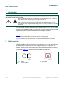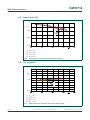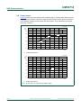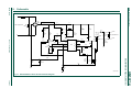
1
UM10714 SSL5301DB1213 flyback LED driver Rev. 1 — 4 June 2014 User manual Document information Info Content Keywords SSL5301DB1213, dimmable, LED driver, flyback converter, A19 Abstract This user manual describes the operation of the SSL5301DB1213 230 V 12 W dimmable LED driver featuring the SSL5301 using a flyback topology. The SSL5301DB1213 demo board has a form factor that is compatible with the base of an A19 LED lamp fitting used in Solid State Lighting (SSL) applications. UM10714 NXP Semiconductors SSL5301DB1213 flyback LED driver Revision history Rev Date Description v.1 20140604 first issue Contact information For more information, please visit: http://www.nxp.com For sales office addresses, please send an email to: [email protected] UM10714 User manual All information provided in this document is subject to legal disclaimers. Rev. 1 — 4 June 2014 © NXP Semiconductors N.V. 2014. All rights reserved. 2 of 21 UM10714 NXP Semiconductors SSL5301DB1213 flyback LED driver 1. Introduction WARNING Lethal voltage and fire ignition hazard The non-insulated high voltages that are present when operating this product, constitute a risk of electric shock, personal injury, death and/or ignition of fire. This product is intended for evaluation purposes only. It shall be operated in a designated test area by personnel qualified according to local requirements and labor laws to work with non-insulated mains voltages and high-voltage circuits. This product shall never be operated unattended. This user manual describes the operation of the SSL5301DB1213 230 V 12 W dimmable LED driver featuring the SSL5301. The SSL5301DB1213 demo board incorporates an A19 LED lamp compatible form factor. The flyback converter topology provides a simple and efficient solution for mains dimmable LED recessed light applications. The SSL5301DB1213 demo board complies with EMI and safety regulations. Figure 2 shows the SSL5301DB1213 demo board dimensions. The design and the components used ensure that the board fits into an A19 lamp base. Figure 3 shows the top view and bottom view of the SSL5301DB1213 demo board. 2. Safety warning The SSL5301DB1213 demo board input is connected to the 230 V mains. Avoid touching the board while it is connected to the mains voltage and when it is in operation. An isolated housing is obligatory when used in uncontrolled, non-laboratory environments. Galvanic isolation from the mains phase using a fixed or variable transformer is always recommended. Figure 1 shows the symbols that identify these devices. 019aab174 019aab173 a. Isolated Fig 1. UM10714 User manual b. Not isolated Isolation symbols All information provided in this document is subject to legal disclaimers. Rev. 1 — 4 June 2014 © NXP Semiconductors N.V. 2014. All rights reserved. 3 of 21 UM10714 NXP Semiconductors SSL5301DB1213 flyback LED driver 3. Specifications Table 1 lists the specifications of the demo board. Table 1. SSL5301DB1213 specifications Symbol Parameter Value Vmains AC mains supply voltage 230 V 15 % Imains AC mains input current < 65 mA VLED output voltage 36 V (range: 30 V to 40 V) ILED output current 250 mA Io(ripple)LED LED output current ripple 30 % efficiency 85 % PF Power Factor > 0.9 at Vmains = 230 V (AC) THD Total Harmonic Distortion 12 % at Vmains = 230 V (AC) and VO(LED) = 40 V (DC) Toper operating temperature 30 C to +100 C fsw switching frequency 60 kHz Figure 2 shows the dimensions of the demo board. Fig 2. UM10714 User manual SSL5301DB1213 demo board dimensions All information provided in this document is subject to legal disclaimers. Rev. 1 — 4 June 2014 © NXP Semiconductors N.V. 2014. All rights reserved. 4 of 21 UM10714 NXP Semiconductors SSL5301DB1213 flyback LED driver 4. Board photographs a. Top view Fig 3. b. Bottom view SSL5301DB1213 demo board 5. Board connections The board is optimized for a 230 V/50 Hz mains supply. In addition to the mains voltage optimization, the board is designed to work with multiple LEDs or an LED module with a 40 V forward voltage. The mains connection of the SSL5301DB1213 demo board is different from other general evaluation/reference boards. Connect the mains to the crew connector CN1 (see Figure 4). Remark: The maximum rated voltage of the board is 265 V (AC). The anode of the LED load is connected to V+ of connector CN2 (see Figure 4). The cathode is connected to V of connector CN2. Use an LED string with a forward voltage between 30 V and 40 V on this demo board. Under the expected conditions, the output current is 250 mA when no dimmer is used. Fig 4. UM10714 User manual SSL5301DB1213 board connections All information provided in this document is subject to legal disclaimers. Rev. 1 — 4 June 2014 © NXP Semiconductors N.V. 2014. All rights reserved. 5 of 21 UM10714 NXP Semiconductors SSL5301DB1213 flyback LED driver 6. Performance The performance was measured using an LED with a 40 V forward voltage at a 250 mA output load. Figure 5 to Figure 11 show the performance data. 6.1 Efficiency DDD Ș 9L9 (1) VLED = 31 V (2) VLED = 34 V (3) VLED = 37 V (4) VLED = 40 V Fig 5. UM10714 User manual Efficiency as a function of AC mains input voltage All information provided in this document is subject to legal disclaimers. Rev. 1 — 4 June 2014 © NXP Semiconductors N.V. 2014. All rights reserved. 6 of 21 UM10714 NXP Semiconductors SSL5301DB1213 flyback LED driver 6.2 Power Factor (PF) DDD 3) 9L9 (1) VLED = 31 V (2) VLED = 34 V (3) VLED = 37 V (4) VLED = 40 V Fig 6. Power factor as a function of AC mains input voltage 6.3 Line regulation DDD ,/(' $ 9L9 (1) VLED = 31 V (2) VLED = 34 V (3) VLED = 37 V (4) VLED = 40 V Fig 7. UM10714 User manual Output current as a function of AC mains input voltage All information provided in this document is subject to legal disclaimers. Rev. 1 — 4 June 2014 © NXP Semiconductors N.V. 2014. All rights reserved. 7 of 21 UM10714 NXP Semiconductors SSL5301DB1213 flyback LED driver 6.4 Load regulation DDD ,/(' $ 9/('9 Fig 8. UM10714 User manual Output current as a function of output voltage at Vi = 230 V (AC) All information provided in this document is subject to legal disclaimers. Rev. 1 — 4 June 2014 © NXP Semiconductors N.V. 2014. All rights reserved. 8 of 21 UM10714 NXP Semiconductors SSL5301DB1213 flyback LED driver 6.5 Dimming curves Figure 9 shows the output current for a leading-edge dimmer and a trailing-edge dimmer. The output current without dimmer is also indicated. The maximum output current with dimmer equals 92 % of the output current when no dimmer is used. As a result, the input power of the SSL5301DB1213 demo board is the same with no dimmer as with dimmer and set at its maximum angle. DDD ,/(' QRGLPPHU Į a. Leading-edge dimming DDD ,/(' QRGLPPHU Į b. Trailing-edge dimming Fig 9. Output current as a function of dimmer angle Dimming compatibility includes smooth dimming without any flashing or flickering effects across the complete dimming range. The SSL5301DB1213 demo board has been tested with a wide selection of dimmers. It is compatible with most leading-edge and trailing-edge dimmers on the market. UM10714 User manual All information provided in this document is subject to legal disclaimers. Rev. 1 — 4 June 2014 © NXP Semiconductors N.V. 2014. All rights reserved. 9 of 21 UM10714 NXP Semiconductors SSL5301DB1213 flyback LED driver 6.6 Power losses Figure 10 shows the power losses when a leading-edge or a trailing-edge dimmer is used. The power losses when no dimmer is used are also indicated. Power losses are defined as the difference between input power and output power. They indicate the total power loss in the converter. DDD QRGLPPHU 3ORVV : Į a. Leading-edge dimmer DDD 3ORVV : QRGLPPHU Į b. Trailing-edge dimmer Fig 10. Power losses as a function of dimmer angle UM10714 User manual All information provided in this document is subject to legal disclaimers. Rev. 1 — 4 June 2014 © NXP Semiconductors N.V. 2014. All rights reserved. 10 of 21 UM10714 NXP Semiconductors SSL5301DB1213 flyback LED driver 6.7 ElectroMagnetic Interference (EMI) The ElectroMagnetic Interference (EMI) was measured according to the EN55015 standard. The board complies with the requirement (see Figure 11). a. Live b. Neutral Fig 11. Conducted emission performance DDD DDD QRLVHOHYHO G%VP QRLVHOHYHO G%VP I0+] a. Horizontal I0+] b. Vertical Fig 12. Radiated emission performance UM10714 User manual All information provided in this document is subject to legal disclaimers. Rev. 1 — 4 June 2014 © NXP Semiconductors N.V. 2014. All rights reserved. 11 of 21 UM10714 NXP Semiconductors SSL5301DB1213 flyback LED driver 7. Protections The IC incorporates the following protections: • • • • • • • • • UnderVoltage LockOut (UVLO) OverCurrent Protection (OCP) Brownout protection Output Short Protection (OSP) Output open OverVoltage Protection (OVP) Internal OverTemperature Protection (OTP) Mains synchronization loss protection Leading-Edge Blanking (LEB) Bleeder dissipation protection Output open OVP is a latched protection. Power-off cycling is required to exit the latched state. All other protections are not latched and lead to a safe restart of the converter. For more information about the protections, see the SSL5301 data sheet (Ref. 1). UM10714 User manual All information provided in this document is subject to legal disclaimers. Rev. 1 — 4 June 2014 © NXP Semiconductors N.V. 2014. All rights reserved. 12 of 21 xxxxxxxxxxxxxxxxxxxxx xxxxxxxxxxxxxxxxxxxxxxxxxx xxxxxxx x x x xxxxxxxxxxxxxxxxxxxxxxxxxxxxxx xxxxxxxxxxxxxxxxxxx xx xx xxxxx xxxxxxxxxxxxxxxxxxxxxxxxxxx xxxxxxxxxxxxxxxxxxx xxxxxx xxxxxxxxxxxxxxxxxxxxxxxxxxxxxxxxxxx xxxxxxxxxxxx x x xxxxxxxxxxxxxxxxxxxxx xxxxxxxxxxxxxxxxxxxxxxxxxxxxxx xxxxx xxxxxxxxxxxxxxxxxxxxxxxxxxxxxxxxxxxxxxxxxxxxxxxxxx xxxxxxxx xxxxxxxxxxxxxxxxxxxxxxxxx xxxxxxxxxxxxxxxxxxxx xxx NXP Semiconductors UM10714 User manual 8. Schematic )6 / ȍ 9$&+] 59 ' %' 0%6 / ' ' 560 560 P+î Rev. 1 — 4 June 2014 All information provided in this document is subject to legal disclaimers. 5 ȍ : 1 5 ȍ : Nȍ & Q) 9 S) 9 =' 0 1 9JV 5 ȍ 4 %& 5 Nȍ ' /(' 5 Nȍ & & Q) 9 5 5 Nȍ & Q) 9 & Q) 9 50 7 P+ ' 560 8 50$,16 9 5 5 0ȍ Nȍ 9&& %/'59 ,& '5$,1 *1' Nȍ 5 QF 5 9P$ Nȍ /(' EODFN 0 1 5 3:5'59 ,616 & ) 9 & Q) 9DF ȍ 5 ȍ %/67& ZKLWH 7 7 5 (6- 5 Nȍ 7 5 Nȍ 5 5 ȍ ' %$6+ 5 ȍ 5 ȍ ' DDD Fig 13. SSL5301DB1213 demo board schematic diagram UM10714 13 of 21 © NXP Semiconductors N.V. 2014. All rights reserved. %$6+ & ) 9 SSL5301DB1213 flyback LED driver 5 ȍ Nȍ UM10714 NXP Semiconductors SSL5301DB1213 flyback LED driver 9. Bill Of Materials (BOM) Table 2. SSL5301DB1213 bill of materials Reference Description and values Part number Manufacturer BD1 bridge rectifier; 0.5 A; 600 V; MB6S; MBS - - C1 capacitor; film; 150 nF; 450 V; 10 %; P = 10 mm; DIP10 C222S154K40C000 Xiamen Fara C2 capacitor; film; 47 nF; 450 V; 10 %; P = 7.5 mm; DIP7.5 CL21-450V-0.047K ZhongShan AIDI Electronics C3 capacitor; film; 150 nF; 450 V; P = 7.5 mm; 10 %; DIP7.5 CL21-450V-0.15K ZhongShan AIDI Electronics C4 capacitor; ceramic; 2.2 nF; 630 V; 10 %; 1206 GHM1530X7R222K630D500 Murata C5 capacitor; electrolysis; 470 F; 50 V; 20 %; 105 °C; 10 mm 20 mm; LK; 8000 h; L-lead - Shanghai Yongming Electronics C7 capacitor; Y; 2.2 nF; 400 V (AC); 10 %; P = 10 mm; DIP10 - - C8 capacitor; ceramic; 220 pF; 50 V; 0805; COG GRM2165C2A221JA01 Murata C10 capacitor; electrolysis; 10 F; 50 V; 20 %;105 °C; 5 mm 11 mm; ELE; 10000 h; axial lead ELE-500ELL220ME11D NCC CN1 connector; L-pin; 2-pin; pitch = 5 mm; DIP2 691312710002 Würth Elektronik CN2 connector; L-pin; 4-pin; pitch = 5 mm; DIP4 691312710004 Würth Elektronik D1; D4; D9 diode; RS1M; 1 A; 700 V; SMA/DO-214AC RS1M Fairchild D2 diode; 1 A; 600 V; ES1J; SMA/DO-214AC ES1J Diotec D7; D8 diode; 0.2 A; 200 V; BAS21H; SOD123 BAS21H NXP Semiconductors FS1 resistor; fusible; 47 ; 2 W; 5 %; axial lead FRN2W47RJ TY-OHM L1 drum inductor; power; 4.7 mH; 0.15 A; 6 8 mm; axial lead - Würth Elektronik M1 N-MOSFET; 1.9 A; 600 V; Vgs = 30 V; ; IPAK/TO251; FQU2N60C Fairchild M2 N-MOSFET; 1.9 A; 600 V; Vgs = 30 V; DPAK/TO252 FQD2N60C Fairchild Q1 transistor; NPN; 0.5 A; 45 V; SOT23 BC817 NXP Semiconductors R1; R2 resistor; chip; 470 k; 1 %; 1206 RC1206FR-07470KL Yageo R3 resistor; chip; 220 k; 5 %; 1206 RC1206JR-13240KL Yageo R5 resistor; fusible; 560 ; 500 V; 3 W; 5 %; axial FRN 3W 560 J TY-OHM R7 resistor; fusible; 750 ; 500 V; 3 W; 5 %; axial FRN 3W 750 J TY-OHM R8 resistor; chip; 30 k; 1 %; 1206 RC1206FR-0730KL Yageo UM10714 User manual All information provided in this document is subject to legal disclaimers. Rev. 1 — 4 June 2014 © NXP Semiconductors N.V. 2014. All rights reserved. 14 of 21 UM10714 NXP Semiconductors SSL5301DB1213 flyback LED driver Table 2. SSL5301DB1213 bill of materials …continued Reference Description and values Part number Manufacturer R10 resistor; chip; 390 k; 1 %; 1206 - Yageo R11 resistor; chip; 18 ; 1 %; 1206 - Yageo R13 resistor; chip; 47 ; 1 %; 0603 RC0603FR-0747RL Yageo R14 resistor; chip; 10 k; 1 %; 0805 RC0603FR-071KL Yageo R17 resistor; chip; 5.6 k; 1 %; 0603 RC0603FR-075K6L Yageo R18 resistor; chip; 10 ; 1 %; 1206 - Yageo R19 resistor; chip; 15 k; 1 %; 0603 RC0603FR-0715KL Yageo R20; R21 resistor; chip; 2.2 ; 1 %; 0805 RC0805FR-072K2L Yageo R23 resistor; chip; 820 ; 1 %; 0603 RC0603FR-07820RL Yageo R24 resistor; chip; 10 ; 1 %; 1206 RC1206FR-1310RL Yageo R25 resistor; chip; 100 k; 1 %; 0603 RT0603FRE07100KL Yageo R26 resistor; chip; 1 M; 1 %; 0603 RC0603FR-071ML Yageo R27 resistor; chip; 470 ; 1 %; 0603 RC0603FR-07470RL Yageo R28 resistor; chip; 4.7 k; 1 %; 1206 - Yageo RV1 surge absorber; 471KD07; 300 V (AC); DIP5 471KD07 BrightKing T1 transformer; RM6; 1.5 mH; RM-6-3 750342290 Würth Elektronik U1 IC; SSL5301; SO-8 SSL5301 NXP Semiconductors ZD1 Zener diode; 5.6 V; 0.55 W; 5 %; SOT323 BZX84J-B5V6 NXP Semiconductors 10. Tuning options To increase dimmer compatibility, decrease the value of bleeder resistor R11 in order. If some smart dimmers cannot start up, try to decrease the resistor R26 value to get a higher start-up current of the bleeder. To achieve a different output current, change the R20 and R21 resistor values. A lower resistance value results in a higher output current. UM10714 User manual All information provided in this document is subject to legal disclaimers. Rev. 1 — 4 June 2014 © NXP Semiconductors N.V. 2014. All rights reserved. 15 of 21 UM10714 NXP Semiconductors SSL5301DB1213 flyback LED driver 11. Board layout Figure 14 shows the SSL5301DB1213 demo board layout of all four layers. Figure 15 show the outer layers of the board with their corresponding silk screen indicating component positions. Red: Top Blue: Bottom Yellow: Silk screen top Gray; Silk screen bottom Fig 14. SSL5301DB1213 demo board with double layers, PCB only UM10714 User manual All information provided in this document is subject to legal disclaimers. Rev. 1 — 4 June 2014 © NXP Semiconductors N.V. 2014. All rights reserved. 16 of 21 UM10714 NXP Semiconductors SSL5301DB1213 flyback LED driver a. Top view b. Bottom view Fig 15. SSL5301DB1213 demo board assembly UM10714 User manual All information provided in this document is subject to legal disclaimers. Rev. 1 — 4 June 2014 © NXP Semiconductors N.V. 2014. All rights reserved. 17 of 21 UM10714 NXP Semiconductors SSL5301DB1213 flyback LED driver 12. Transformer specification $ PLQ NQREGRWORFDWHVWHUP PD[ PD[ PD[ : % WHUPQXPEHUVIRU UHIHUHQFHRQO\ [ SDUWPXVWLQVHUWIXOO\WR VXUIDFH$LQUHFRPPHQGHGJULG ORWFRGHDQGGDWHFRGH [ [ 35, 9$& N+] $8; 9$ % 6(& 9$ : [ [ UHFRPPHQGHG SFSDWWHUQFRPSRQHQWVLGH 'LPHQVLRQVLQPP DDD Fig 16. Specification of transformer T1 Table 3. Transformer T1 specifications At 25 C unless otherwise specified. Parameter Value Test conditions maximum 2.97 at 20 C DC resistance 6-4 maximum 0.811 at 20 C DC resistance B-W maximum 0.674 at 20 C inductance 2-3 1.50 mH 7 % 50 kHz; 0.1 V (AC); Ls leakage inductance 2-3 maximum 20 H tie (4 + 6 + B + W); 100 kHz; 0.1 V (AC); Ls dielectric 1-B 4000 V (AC); 1 minute tie (3 + 4); 4000 V (AC); 1 s dielectric B-core 1000 V (AC); 1 minute tie (3 + 4 + B); 1000 V (AC); 1 s dielectric 3-4 1800 V (AC); 1 s 1800 V (AC); 1 s Electric specifications DC resistance 2-3 turns ratio 100T : 24T (2-3) : (6-4) turns ratio 100T : 40T (2-3) : (B-W) 40 C to +125 C including temperature increase General specifications operating temperature UM10714 User manual All information provided in this document is subject to legal disclaimers. Rev. 1 — 4 June 2014 © NXP Semiconductors N.V. 2014. All rights reserved. 18 of 21 UM10714 NXP Semiconductors SSL5301DB1213 flyback LED driver The T1 transformer has been designed to comply with the following requirements as defined by IEC60950-1: • Reinforced insulation for a primary circuit at a 400 V (DC) working voltage. 13. Abbreviations Table 4. Abbreviations Acronym Description EMI ElectroMagnetic Interference LE Leading-Edge LED Light Emitting Diode PF Power Factor SSL Solid-State Lighting TE Trailing-Edge 14. References UM10714 User manual [1] SSL5301 data sheet — Mains dimmable controller for LED lighting [2] AN11533 application note — SSL5301 driver for mains dimmable LED applications All information provided in this document is subject to legal disclaimers. Rev. 1 — 4 June 2014 © NXP Semiconductors N.V. 2014. All rights reserved. 19 of 21 UM10714 NXP Semiconductors SSL5301DB1213 flyback LED driver 15. Legal information 15.1 Definitions Draft — The document is a draft version only. The content is still under internal review and subject to formal approval, which may result in modifications or additions. NXP Semiconductors does not give any representations or warranties as to the accuracy or completeness of information included herein and shall have no liability for the consequences of use of such information. NXP Semiconductors does not accept any liability related to any default, damage, costs or problem which is based on any weakness or default in the customer’s applications or products, or the application or use by customer’s third party customer(s). Customer is responsible for doing all necessary testing for the customer’s applications and products using NXP Semiconductors products in order to avoid a default of the applications and the products or of the application or use by customer’s third party customer(s). NXP does not accept any liability in this respect. Export control — This document as well as the item(s) described herein may be subject to export control regulations. Export might require a prior authorization from competent authorities. 15.2 Disclaimers Limited warranty and liability — Information in this document is believed to be accurate and reliable. However, NXP Semiconductors does not give any representations or warranties, expressed or implied, as to the accuracy or completeness of such information and shall have no liability for the consequences of use of such information. NXP Semiconductors takes no responsibility for the content in this document if provided by an information source outside of NXP Semiconductors. In no event shall NXP Semiconductors be liable for any indirect, incidental, punitive, special or consequential damages (including - without limitation - lost profits, lost savings, business interruption, costs related to the removal or replacement of any products or rework charges) whether or not such damages are based on tort (including negligence), warranty, breach of contract or any other legal theory. Notwithstanding any damages that customer might incur for any reason whatsoever, NXP Semiconductors’ aggregate and cumulative liability towards customer for the products described herein shall be limited in accordance with the Terms and conditions of commercial sale of NXP Semiconductors. Right to make changes — NXP Semiconductors reserves the right to make changes to information published in this document, including without limitation specifications and product descriptions, at any time and without notice. This document supersedes and replaces all information supplied prior to the publication hereof. Suitability for use — NXP Semiconductors products are not designed, authorized or warranted to be suitable for use in life support, life-critical or safety-critical systems or equipment, nor in applications where failure or malfunction of an NXP Semiconductors product can reasonably be expected to result in personal injury, death or severe property or environmental damage. NXP Semiconductors and its suppliers accept no liability for inclusion and/or use of NXP Semiconductors products in such equipment or applications and therefore such inclusion and/or use is at the customer’s own risk. Applications — Applications that are described herein for any of these products are for illustrative purposes only. NXP Semiconductors makes no representation or warranty that such applications will be suitable for the specified use without further testing or modification. Customers are responsible for the design and operation of their applications and products using NXP Semiconductors products, and NXP Semiconductors accepts no liability for any assistance with applications or customer product design. It is customer’s sole responsibility to determine whether the NXP Semiconductors product is suitable and fit for the customer’s applications and products planned, as well as for the planned application and use of customer’s third party customer(s). Customers should provide appropriate design and operating safeguards to minimize the risks associated with their applications and products. Evaluation products — This product is provided on an “as is” and “with all faults” basis for evaluation purposes only. NXP Semiconductors, its affiliates and their suppliers expressly disclaim all warranties, whether express, implied or statutory, including but not limited to the implied warranties of non-infringement, merchantability and fitness for a particular purpose. The entire risk as to the quality, or arising out of the use or performance, of this product remains with customer. In no event shall NXP Semiconductors, its affiliates or their suppliers be liable to customer for any special, indirect, consequential, punitive or incidental damages (including without limitation damages for loss of business, business interruption, loss of use, loss of data or information, and the like) arising out the use of or inability to use the product, whether or not based on tort (including negligence), strict liability, breach of contract, breach of warranty or any other theory, even if advised of the possibility of such damages. Notwithstanding any damages that customer might incur for any reason whatsoever (including without limitation, all damages referenced above and all direct or general damages), the entire liability of NXP Semiconductors, its affiliates and their suppliers and customer’s exclusive remedy for all of the foregoing shall be limited to actual damages incurred by customer based on reasonable reliance up to the greater of the amount actually paid by customer for the product or five dollars (US$5.00). The foregoing limitations, exclusions and disclaimers shall apply to the maximum extent permitted by applicable law, even if any remedy fails of its essential purpose. Safety of high-voltage evaluation products — The non-insulated high voltages that are present when operating this product, constitute a risk of electric shock, personal injury, death and/or ignition of fire. This product is intended for evaluation purposes only. It shall be operated in a designated test area by personnel that is qualified according to local requirements and labor laws to work with non-insulated mains voltages and high-voltage circuits. The product does not comply with IEC 60950 based national or regional safety standards. NXP Semiconductors does not accept any liability for damages incurred due to inappropriate use of this product or related to non-insulated high voltages. Any use of this product is at customer’s own risk and liability. The customer shall fully indemnify and hold harmless NXP Semiconductors from any liability, damages and claims resulting from the use of the product. Translations — A non-English (translated) version of a document is for reference only. The English version shall prevail in case of any discrepancy between the translated and English versions. 15.3 Trademarks Notice: All referenced brands, product names, service names and trademarks are the property of their respective owners. GreenChip — is a trademark of NXP Semiconductors N.V. UM10714 User manual All information provided in this document is subject to legal disclaimers. Rev. 1 — 4 June 2014 © NXP Semiconductors N.V. 2014. All rights reserved. 20 of 21 UM10714 NXP Semiconductors SSL5301DB1213 flyback LED driver 16. Contents 1 2 3 4 5 6 6.1 6.2 6.3 6.4 6.5 6.6 6.7 7 8 9 10 11 12 13 14 15 15.1 15.2 15.3 16 Introduction . . . . . . . . . . . . . . . . . . . . . . . . . . . . 3 Safety warning . . . . . . . . . . . . . . . . . . . . . . . . . . 3 Specifications. . . . . . . . . . . . . . . . . . . . . . . . . . . 4 Board photographs . . . . . . . . . . . . . . . . . . . . . . 5 Board connections . . . . . . . . . . . . . . . . . . . . . . 5 Performance . . . . . . . . . . . . . . . . . . . . . . . . . . . . 6 Efficiency . . . . . . . . . . . . . . . . . . . . . . . . . . . . . 6 Power Factor (PF) . . . . . . . . . . . . . . . . . . . . . . 7 Line regulation . . . . . . . . . . . . . . . . . . . . . . . . . 7 Load regulation . . . . . . . . . . . . . . . . . . . . . . . . . 8 Dimming curves . . . . . . . . . . . . . . . . . . . . . . . . 9 Power losses . . . . . . . . . . . . . . . . . . . . . . . . . 10 ElectroMagnetic Interference (EMI) . . . . . . . . 11 Protections . . . . . . . . . . . . . . . . . . . . . . . . . . . . 12 Schematic . . . . . . . . . . . . . . . . . . . . . . . . . . . . . 13 Bill Of Materials (BOM) . . . . . . . . . . . . . . . . . . 14 Tuning options . . . . . . . . . . . . . . . . . . . . . . . . . 15 Board layout . . . . . . . . . . . . . . . . . . . . . . . . . . . 16 Transformer specification . . . . . . . . . . . . . . . . 18 Abbreviations . . . . . . . . . . . . . . . . . . . . . . . . . . 19 References . . . . . . . . . . . . . . . . . . . . . . . . . . . . 19 Legal information. . . . . . . . . . . . . . . . . . . . . . . 20 Definitions . . . . . . . . . . . . . . . . . . . . . . . . . . . . 20 Disclaimers . . . . . . . . . . . . . . . . . . . . . . . . . . . 20 Trademarks. . . . . . . . . . . . . . . . . . . . . . . . . . . 20 Contents . . . . . . . . . . . . . . . . . . . . . . . . . . . . . . 21 Please be aware that important notices concerning this document and the product(s) described herein, have been included in section ‘Legal information’. © NXP Semiconductors N.V. 2014. All rights reserved. For more information, please visit: http://www.nxp.com For sales office addresses, please send an email to: [email protected] Date of release: 4 June 2014 Document identifier: UM10714