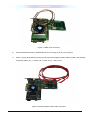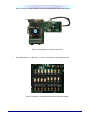
1
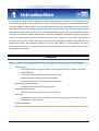
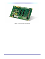
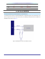
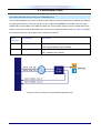
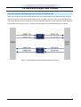
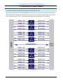
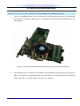
Terasic THDB-H2G
VERSION 1.0
March 1, 2010
Copyright © 2003-2010 Terasic Technologies Inc. All Rights Reserved.
Introduction
Page Index
INTRODUCTION ..............................................................................................................................................................................1
1.1 FEATURES ....................................................................................................................................................................................1
1.2 ABOUT THE KIT............................................................................................................................................................................3
1.3 GETTING HELP.............................................................................................................................................................................3
ARCHITECTURE .............................................................................................................................................................................3
2.1 LAYOUT AND COMPONETS ...........................................................................................................................................................3
2.2 BLOCK DIAGRAM..........................................................................................................................................................................7
BOARD COMPONENTS.................................................................................................................................................................8
3.1 HSMC EXPANSION CONNECTOR ................................................................................................................................................8
3.2 I2C SERIAL EEPROM ..............................................................................................................................................................16
3.3 SATA/SAS CLOCK ....................................................................................................................................................................17
3.4 SATA/SAS SINGLE LANE CHANNEL .........................................................................................................................................18
3.5 SATA/SAS 4 LANE CHANNEL ...................................................................................................................................................19
3.6 CONFIGURATION, STATUS AND SETUP ELEMENTS....................................................................................................................20
3.4 ATX POWER ..............................................................................................................................................................................21
DEMONSTRATION........................................................................................................................................................................22
4.1 INTRODUCTION...........................................................................................................................................................................22
4.2 SYSTEM REQUIREMENTS ..........................................................................................................................................................23
4.3 SETUP THE DEMONSTRATION ....................................................................................................................................................24
4.4 DEMO OPERATION .....................................................................................................................................................................27
APPENDIX ......................................................................................................................................................................................27
5.1 REVISION HISTORY ....................................................................................................................................................................27
5.2 ALWAYS VISIT SATA W EBPAGE FOR NEW MAIN BOARD ...........................................................................................................27
ii
Introduction
1
Introduction
The SATA/SAS daughter card is designed to provide SATA interface conversion for FPGA platforms that
support SAS and SATA solutions based on the latest 40-nm technology through a High-Speed Mezzanine
Connector (HSMC). It allows users to access storage devices through the SATA/SAS protocols on an FPGA
specifically the Stratix IV GX, Stratix II GX, Arria II GX, and Cyclone IV GX devices. This card features 4 single
channel SATA signal plug connectors, one 4 channel SATA/SAS connector, and one ATX style output power
connector for hard drives. With the SATA interface conversion established on the HSMC interface, your FPGA
system can bridge different protocols enabling the FPGA to be a system on chip (SOC), plus with the
SATA/SAS IP core on the FPGA it can be used for functionality, specification-compliance, interoperability, and
performance testing. The SATA/SAS daughter card is the ideal platform for SATA interface conversion
ensuring an excellent way to develop SOC solutions for storage applications on the Altera’s 40-nm FPGAs
with integrated transceivers.
1.1 Features
1-1
Figure 1.1 shows the photo of the SATA/SAS card. The important functions of the card are listed below:
•
HSMC interface
o
8 high speed interfaces supporting SATA / SAS communications at 1.5Gbps, 3 Gbps and
6Gbps data rates
•
o
6 out-of-band signals supported for the 4 lane connector
o
Dipswitch inputs on CMOS input section of HSMC
o
LED drive outputs for 16 bi-color LEDs (32 connections)
SATA/SAS Single lane interface
o
•
SATA/SAS 4 lane interface
o
•
Internal style vertical surface mount connectors
Internal style 32 pin vertical surface mount connector
ATX power
o
Standard ATX 4 pin connector providing 1 Amp on both 12V and 5V power rails from host
boards able to support current
•
8 Kbit I2C EEPROM
•
Differential clocking for 150MHz and 300MHz reference clocks through the HSMC or SMA connectors
1
Introduction
Figure 1.1. The picture of the SATA/SAS card
2
Introduction
1.2 About the KIT
This section describes the package content
•
SATA/SAS HSMC card x 1
•
SATA crossover ribbon cable x 2
•
System CD-ROM x 1
* The SATA crossover ribbon cable is only used for loopback testing purposes. Please do not attempt to
connect SATA hard-disk using this cable.
The CD contains technical documents of the SATA/SAS card
Figure 1.2 SATA/SAS card Package
1.3 Getting Help
1-2
Here are some places to get help if you encounter any problem:
Email to [email protected]
Taiwan & China: +886-3-550-8800
Korea : +82-2-512-7661
Japan: +81-428-77-7000
3
Architecture
2
Architecture
This chapter describes the architecture of the SATA/SAS card including block diagram and components.
2.1 Layout and Componets
1-3
The picture of the SATA/SAS card is shown in Figure 2.1 and Figure 2.2. It depicts the layout of the board and
indicates the locations of the connectors and key components.
4
Architecture
User Dip SW
Power
5V
12V
SMA
SATA_CLK_OUT
CLK_OE,
CLK_FS
ATX
Power
SATA/SAS Single Lane Channels
RX0 TX0
LEDs
RX1 TX1
LEDs
SATA/SAS 4x Channel
RX/TX 4-7
LEDs
Figure 2.1 The SATA/SAS Card PCB and component diagram
5
Architecture
Figure 2.2 The SATA/SAS card back side – HSMC connector view
The following components are provided on the SATA/SAS card :
•
HSMC Connector (J12)
•
User Dip SW (SW1)
•
SMA SATA_CLK_OUT (J1/J2)
•
SATA/SAS Single Lane Channels (J3/J4/J8/J9)
•
SATA/SAS 4x Channel (J5)
•
ATX Power (J11)
•
CLK_OE (J6), CLK_FS (J7)
6
Architecture
2.2 Block Diagram
1-4
Figure 2.3 shows the block diagram of the SATA/SAS card.
Figure 2.3. The block diagram of the SATA/SAS Card
7
Board Components
3
Board Components
This section will describe the detailed information of the components, connector interfaces,
and the pin mappings on the SATA/SAS card.
3.1 HSMC Expansion Connector
1-5
This section describes the HSMC connector on the SATA/SAS card
The SATA/SAS card contains an Altera standard HSMC connector. All the other interfaces on the SATA/SAS
card are connected to the HSMC connector. Figure 3.1 shows the pin-outs of the HSMC connector and Table
3.1 lists the description of each signals corresponding to the HSMC connector.
8
Board Components
Figure 3.1 The pin-outs of the HSMC connector.
9
Board Components
Table 3.1 below lists the HSMC signal direction and description
Pin
Name
Numbers
1
Direction (with respect
Description
to the FPGA board)
HSM_TX_P7
Output
Differential transmit data output
before DC blocking capacitor
2
HSM_RX_P7
Input
Differential transmit data input
before DC blocking capacitor
3
HSM_TX_N7
Output
Differential transmit data output
before DC blocking capacitor
4
HSM_RX_N7
Input
Differential transmit data input
before DC blocking capacitor
5
HSM_TX_P6
Output
Differential transmit data output
before DC blocking capacitor
6
HSM_RX_P6
Input
Differential transmit data input
before DC blocking capacitor
7
HSM_TX_N6
Output
Differential transmit data output
before DC blocking capacitor
8
HSM_RX_N6
Input
Differential transmit data input
before DC blocking capacitor
9
HSM_TX_P5
Output
Differential transmit data output
before DC blocking capacitor
10
HSM_RX_P5
Input
Differential transmit data input
before DC blocking capacitor
11
HSM_TX_N5
Output
Differential transmit data output
before DC blocking capacitor
12
HSM_RX_N5
Input
Differential transmit data input
before DC blocking capacitor
13
HSM_TX_P4
Output
Differential transmit data output
before DC blocking capacitor
14
HSM_RX_P4
Input
Differential transmit data input
before DC blocking capacitor
15
HSM_TX_N4
Output
Differential transmit data output
before DC blocking capacitor
16
HSM_RX_N4
Input
Differential transmit data input
before DC blocking capacitor
17
HSM_TX_P3
Output
Differential transmit data output
before DC blocking capacitor
18
HSM_RX_P3
Input
Differential transmit data input
before DC blocking capacitor
10
Board Components
19
HSM_TX_N3
Output
Differential transmit data output
before DC blocking capacitor
20
HSM_RX_N3
Input
Differential transmit data input
before DC blocking capacitor
21
HSM_TX_P2
Output
Differential transmit data output
before DC blocking capacitor
22
HSM_RX_P2
Input
Differential transmit data input
before DC blocking capacitor
23
HSM_TX_N2
Output
Differential transmit data output
before DC blocking capacitor
24
HSM_RX_N2
Input
Differential transmit data input
before DC blocking capacitor
25
HSM_TX_P1
Output
Differential transmit data output
before DC blocking capacitor
26
HSM_RX_P1
Input
Differential transmit data input
before DC blocking capacitor
27
HSM_TX_N1
Output
Differential transmit data output
before DC blocking capacitor
28
HSM_RX_N1
Input
Differential transmit data input
before DC blocking capacitor
29
HSM_TX_P0
Output
Differential transmit data output
before DC blocking capacitor
30
HSM_RX_P0
Input
Differential transmit data input
before DC blocking capacitor
31
HSM_TX_N0
Output
Differential transmit data output
before DC blocking capacitor
32
HSM_RX_N0
Input
Differential transmit data input
before DC blocking capacitor
33
SMB_SDA
Inout
I2C
EEPROM
address/data I/O
34
SMB_SCL
Inout
35
-
-
-
36
-
-
-
37
JTAG_TDO_TDI
Inout
JTAG
38
JTAG_TDO_TDI
Inout
JTAG
39
-
-
-
40
-
-
-
41
SATA_RX_LED_
Output
R7
11
I2C EEPROM serial clock
Red LED signal
serial
Board Components
42
USER_DIPSW7
Input
43
SATA_RX_LED_
Output
User control input from dipswitch
Green LED signal
G7
44
USER_DIPSW6
Input
User control input from dipswitch
45
3V3
Power
Power 3.3V
46
12V
Power
Power 12V
47
SATA_RX_LED_
Output
Red LED signal
R6
48
USER_DIPSW5
Input
49
SATA_RX_LED_
Output
User control input from dipswitch
Green LED signal
G6
50
USER_DIPSW4
Input
User control input from dipswitch
51
3V3
Power
Power 3.3V
52
12V
Power
Power 12V
53
SATA_RX_LED_
Output
Red LED signal
R5
54
USER_DIPSW3
Input
55
SATA_RX_LED_
Output
User control input from dipswitch
Green LED signal
G5
56
USER_DIPSW2
Input
User control input from dipswitch
57
3V3
Power
Power 3.3V
58
12V
Power
Power 12V
59
SATA_RX_LED_
Output
Red LED signal
R4
60
USER_DIPSW1
Input
61
SATA_RX_LED_
Output
User control input from dipswitch
Green LED signal
G4
62
USER_DIPSW0
Input
User control input from dipswitch
63
3V3
Power
Power 3.3V
64
12V
Power
Power 12V
65
SATA_RX_LED_
Output
Red LED signal
R3
66
-
-
67
SATA_RX_LED_
Output
Green LED signal
G3
68
-
-
69
3V3
Power
Power 3.3V
70
12V
Power
Power 12V
71
SATA_RX_LED_
Output
Red LED signal
12
-
Board Components
R2
72
-
-
73
SATA_RX_LED_
Output
Green LED signal
G2
74
-
-
-
75
3V3
Power
Power 3.3V
76
12V
Power
Power 12V
77
SATA_RX_LED_
Output
Red LED signal
R1
78
-
-
79
SATA_RX_LED_
Output
Green LED signal
G1
80
-
-
-
81
3V3
Power
Power 3.3V
82
12V
Power
Power 12V
83
SATA_RX_LED_
Output
Red LED signal
R0
84
SAS_SIDEBAND
Inout
0
85
SATA_RX_LED_
4
lane
SATA/SAS
sideband
signal
Output
Green LED signal
G0
86
SAS_SIDEBAND
Inout
1
4
lane
SATA/SAS
sideband
signal
87
3V3
Power
Power 3.3V
88
12V
Power
Power 12V
89
SATA_TX_LED_
Output
Red LED signal
R7
90
SAS_SIDEBAND
Inout
2
91
SATA_TX_LED_
4
lane
SATA/SAS
sideband
signal
Output
Green LED signal
G7
92
SAS_SIDEBAND
Inout
3
4
lane
SATA/SAS
sideband
signal
93
3V3
Power
Power 3.3V
94
12V
Power
Power 12V
95
SATA_TX_LED_
Output
Red LED signal
R6
96
SAS_SIDEBAND
Inout
4
4
lane
signal
13
SATA/SAS
sideband
Board Components
97
SATA_TX_LED_
Output
Green LED signal
G6
98
SAS_SIDEBAND
Inout
5
4
lane
SATA/SAS
signal
99
3V3
Power
Power 3.3V
100
12V
Power
Power 12V
101
SATA_TX_LED_
Output
Red LED signal
R5
102
-
-
103
SATA_TX_LED_
Output
Green LED signal
G5
104
-
-
-
105
3V3
Power
Power 3.3V
106
12V
Power
Power 12V
107
SATA_TX_LED_
Output
Red LED signal
R4
108
-
-
109
SATA_TX_LED_
Output
Green LED signal
G4
110
-
-
-
111
3V3
Power
Power 3.3V
112
12V
Power
Power 12V
113
SATA_TX_LED_
Output
Red LED signal
R3
114
-
-
115
SATA_TX_LED_
Output
Green LED signal
G3
116
-
-
-
117
3V3
Power
Power 3.3V
118
12V
Power
Power 12V
119
SATA_TX_LED_
Output
Red LED signal
R2
120
-
-
121
SATA_TX_LED_
Output
Green LED signal
G2
122
-
-
123
3V3
Power
Power 3.3V
124
12V
Power
Power 12V
125
SATA_TX_LED_
Output
Red LED signal
14
-
sideband
Board Components
R1
126
-
-
127
SATA_TX_LED_
Output
Green LED signal
G1
128
-
-
-
129
3V3
Power
Power 3.3V
130
12V
Power
Power 12V
131
SATA_TX_LED_
Output
Red LED signal
R0
132
-
-
133
SATA_TX_LED_
Output
Green LED signal
G0
134
-
-
-
135
3V3
Power
Power 3.3V
136
12V
Power
Power 12V
137
SATA_CLK_OE
Output
Oscillator clock output enable
(Active High)
138
SATA_CLK_FS
Output
150MHz/300MHz
oscillator
frequency select
139
-
-
-
140
-
-
-
141
3V3
Power
Power 3.3V
142
12V
Power
Power 12V
143
-
-
-
144
-
-
-
145
-
-
-
146
-
-
-
147
3V3
Power
Power 3.3V
148
12V
Power
Power 12V
149
-
-
-
150
-
-
-
151
-
-
-
152
-
-
-
153
3V3
Power
Power 3.3V
154
12V
Power
Power 12V
155
-
-
156
SATA_HSM_CLK
Input
_P
157
-
150MHz/300MHz
clock
15
-
differential
Board Components
158
SATA_HSM_CLK
Input
_N
150MHz/300MHz
differential
clock
159
3V3
Power
Power 3.3V
160
HSM_PSNTn
Power
Power Ground
3.2 I2C Serial EEPROM
1-6
This section describes the I2C Serial EEPROM on the SATA/SAS card
The SATA/SAS card consists of an 8 Kbit EEPROM which is configured through a 2-wire serial interface. The
device is organized as four blocks of 256 x 8-bit memory. The detailed pin description between the HSMC and
EEPROM is shown below in Figure 3.2.
Figure 3.2 EEPROM connection to the HSMC connector
16
Board Components
3.3 SATA/SAS Clock
1-7
This section describes clock circuitry on the SATA/SAS card
The on-board oscillator is to provide a clean low jitter reference clock at frequencies of 150MHz and 300MHz
by toggling the frequency select pin (FS) for use in the high-speed SERDES TX and RX, while the output
enable (OE) of the oscillator will tri-state the output pins. The oscillator output is driven to a differential clock
buffer to provide two identical differential clock outputs to the HSMC and SMA connectors. Figure 3.3 depicts
the connection made on the oscillator clocks and SMA connectors.
Board
Signal Name
Description
CLK_OE
Jumper DNI – clock output enabled (default), Jumper Installed –
Reference
J6
clock output disabled (outputs tristated)
J7
CLK_FS
Jumper Installed – 150MHz clock selected (default), Jumper
DNI – 300MHz clock selected
Figure 3.3 Clock connection on the SATA/SAS daughter card
17
Board Components
3.4 SATA/SAS Single Lane Channel
1-8
This section describes SATA/SAS single lane channel on the SATA/SAS card
There are 4 single channel SATA single channel links which are facilitated on the SATA/SAS card using the
passive connection from the high-speed serial link from the HSMC connector to the 7-pin SATA signal plugs.
The routing between the two connectors is 100 Ohm differential impedance route with DC blocking capacitors
in the middle of the channel. Figure 3.4 depicts a block diagram of the SATA/SAS single lane channel.
Figure 3.4 Block diagram of the SATA/SAS single lane channel
18
Board Components
3.5 SATA/SAS 4 Lane Channel
1-9
This section describes SATA/SAS 4 lane channel on the SATA/SAS card
A 32 pins signal connector is used for SATA/SAS quad channel link. The connector contains 16 high-speed
differential signals for SATA/SAS communications protocol. There are 10 pins used for signal ground and 6
pins for sideband signals. Figure 3.5 shows the block diagram of the SATA/SAS 4 lane channel.
Figure 3.5 block diagram of the SATA/SAS 4 lane channel
19
Board Components
3.6 Configuration, Status and Setup Elements
1-10
This section describes the configuration, status and setup elements of the SATA/SAS card
Configuration:
A jumper (J10) is available to disable the 12V to 5V regulator. If the on-board power output connector is not
used it is recommended that the switching regulator be disabled by placing this jumper.
Setup:
An eight position user dip switch shown in Figure 3.6 is supplied on the board to enable developers to have
application specific user supplied setting. The dip switched is configured so that in the shorted position the
higher number pins (9-16) are shorted to ground. The lower number pins (1-8) are connected to user signals
that are attached to the HSMC lower speed signaling. The user dip switch can be used to control various
modes depending on the user design. As with any user interface proper de-bouncing counters and
synchronization circuitry is required for any proper design.
Figure 3.6 Eight position user dip switch
Status LEDs:
Component reference for LEDs describes board reference description signaling standard for the LEDs
located on the SATA/SAS card. Each channel has a bi-colored LED for TX and RX
LED
Color
Description
D5
Blue
5V power
D9, D11, D2, D4
Bi-color Off/Red/Green/Orange
SATA/SAS transmit status (user function driven)
(single lane transmit channels)
D8, D10, D1, D3
Bi-color Off/Red/Green/Orange
SATA/SAS receive status (user function driven)
(singe lane receive channels
D16, D17, D18,
Bi-color off/Red/Green/Orange
20
SATA/SAS transmit status (user function driven)
Board Components
D19
(4 lane transmit channel)
D12, D13, D14,
Bi-color off/Red/Green/Orange
D15
(4 lane receive channel)
SATA/SAS receive status (user function driven)
3.4 ATX Power
1-11
This section describes the ATX power provided on the SATA/SAS card
The SATA/SAS card consists of an ATX power connector to provide power to an attached disk drive unit. A
switching regulator is used to generate 5V from 12V where the connector is rated to supply 1A of each voltage
for use by the disk drive. Figure 3.7 below shows the power tree of the ATX power connector.
Figure 3.7 Power tree of ATX power connector
21
Demonstration
4
Demonstration
This chapter illustrates the reference design for the SATA/SAS daughter card.
4.1 Introduction
1-12
This section describes the functionality of the demonstration briefly.
The demonstration illustrates a loopback test for transceiver channels using the SATA/SAS daughter card and the
Stratix IV GX development board. There are a total of 2 designs where the SATA reference clock is taken from
different locations, HSMC connector and SMA connector respectively therefore either one can be driven. Note that if
you select the HSMC connector to drive the SATA reference clock, a connection using the SMA cable is not required.
Users have the option of connecting the loopback connection to the single channels of the SATA connector or
establishing the connection using the SATA/SAS 4x cable. Note that the SATA crossover cables are included in the
kit can be only used on the single channel of the SATA connector. Figure 4.1 and Figure 4.2 depicts the block
diagram for this demonstration. The design will run a well known repeating pattern on 4 or 8 SATA channels
depending on the connection. The demonstration is intended for users to provide a basic instruction to the SATA/SAS
daughter card with the procedures to control different hardware and software settings.
Figure 4.1 Block diagram of the SATA/SAS loopback design using the SATA loopback ribbon cable
22
Demonstration
Figure 4.2 Block diagram of the SATA/SAS loopback design using the SATA/SAS 4x cable
4.2 System Requirements
The following items are required for the SATA/SAS loopback demonstration.
•
SATA/SAS daughter card x 1
•
Stratix IV GX FPGA Development Board x 1
•
SATA loopback crossover signal ribbon cable x 2 (Included in the package)
•
SATA/SAS 4x loopback cable (optional)
•
SMA cable x 2 (If using the SMA SATA reference design)
23
Demonstration
4.3 Setup the Demonstration
Figure 4.3, 4.4, 4.4, 4.5, 4.6, and 4.7 shows how to setup hardware for the SATA demonstration.
i.
Plug in the SATA/SAS daughter card onto the Stratix IV GX development board. Note: The SATA/SAS
card must be connected to HSMC Slot “A” of the Stratix IV GX FPGA Development Board for this
demonstration.
Figure 4.3 Connecting the SATA/SAS daughter card to the Stratix IV development board
ii.
Set S4=[00011011] on the backside of the Stratix IV GX development board, follow by connecting the
SMA clock between the SATA/SAS daughter card and Stratix IV GX development board as follows:
(SATA_CLK_OUT_P ~ CLKIN_P, SATA_CLK_OUT_N ~ CLKIN_N)
24
Demonstration
Figure 4.4 SMA clock connection
iii.
Set the SATA/SAS board for 300MHz REFCLK by removing the CLK_FS (J7) jumper.
iv.
Option 1 (using single SATA channel): Connect the SATA loopback ribbon cable included in the package
as follows: (SATA_CH_2 ~ SATA_CH_3, SATA_CH_0 ~ SATA_CH1)
Figure 4.5 SATA loopback ribbon cable connection
25
Demonstration
Option 2 (using 4x SATA channels): Connect a SATA/SAS 4x cable shown below
Figure 4.6 SATA/SAS 4x loopback connection
v.
Set USER_DIPS 0-3 = ON and 4-7 = OFF on the Stratix IV development board.
Figure 4.7 Stratix IV development board User DIP SW3 settings
26
Demonstration
4.4 Demo Operation
This section describes the procedures of running the demonstration
FPGA Configuration
Demonstration Setup, File Locations, and Instructions
SATA Transceiver Loopback Test Demo using SMA ref clock:
•
Project directory: hsmc_loopback_dev_kit_refclk_s4gx230
•
Bit Stream used: hsmc_loopback.sof
•
Stratix IV GX FPGA Development Kit Setup
•
Set S4=[00011011] on backside of the Stratix IV GX development board.
Set the rotary switch (SW2) to the 0 position
Power
on
the
Stratix
IV
GX
FPGA
Development
Board
and
download
the
SOF
file
(hsmc_loopback_dev_kit_refclk.sof)
•
Press the CPU_RESET pushbutton. USER_LEDS 4-7 will display the “heartbeat” pattern, indicating that
the FPGA’s state machine is running. LEDS (pcie_led_x1, pcie_led_x4, pcie_led_x8, pcie_led_g2) will
also display the “heartbeat pattern”.
•
Refer to Table 4.1 and Table 4.2 for the Pushbuttons and LED definitions.
•
Press and release USER_PB[0]
•
Press and release USER_PB[1]
•
Press and release USER_PB[2]
•
Confirm USER LEDS 0, 1, and 2 illuminate, and USER_LED 3 is not illuminated. All 8 SATA_USER_LEDs
will be GREEN if this step passes.
•
Press both USER_PB[1] and USER_PB[2], then release both will create an error in the transmitter data
stream.
•
Confirm USER_LED 3 is illuminated. All RX_SATA_USER_LEDs for all tested channels will be RED.
•
Simultaneously press USER_PB[0] and USER_PB[1], the SATA_USER_LED will show a moving
ORANGE moving pattern with GREEN background.
•
Simultaneously press USER_PB[0] and USER_PB[2], the SATA_USER_LED will show a moving
ORANGE moving pattern with RED background.
SATA Transceiver Loopback Test Demo using HSMC ref clock:
FPGA Configuration
Demonstration Setup, File Locations, and Instructions
•
Project directory: hsmc_loopback_hsmc_sata_refclk_s4gx230
•
Bit Stream used: hsmc_loopback.sof
•
Stratix IV GX FPGA Development Kit Setup
•
Set S4=[00011011] on backside of the Stratix IV GX development board.
Set the rotary switch (SW2) to the 0 position
Power
on
the
Stratix
IV
GX
FPGA
27
Development
Board
and
download
the
SOF
file
Demonstration
(hsmc_loopback_dev_kit_refclk.sof)
•
Press the CPU_RESET pushbutton. USER_LEDS 4-7 will display the “heartbeat” pattern, indicating that
the FPGA’s state machine is running. LEDS (pcie_led_x1, pcie_led_x4, pcie_led_x8, pcie_led_g2) will
also display the “heartbeat pattern”.
•
Refer to Table 4.1 and Table 4.2 for the Pushbuttons and LED definitions.
•
Press and release USER_PB[0]
•
Press and release USER_PB[1]
•
Press and release USER_PB[2]
•
Confirm USER LEDS 0, 1, and 2 illuminate, and USER_LED 3 is not illuminated. All 8 SATA_USER_LEDs
will be GREEN if this step passes.
•
Press both USER_PB[1] and USER_PB[2], then release both will create an error in the transmitter data
stream.
•
Confirm USER_LED 3 is illuminated. All RX_SATA_USER_LEDs for all tested channels will be RED.
•
Simultaneously press USER_PB[0] and USER_PB[1], the SATA_USER_LED will show a moving
ORANGE moving pattern with GREEN background.
•
Simultaneously press USER_PB[0] and USER_PB[2], the SATA_USER_LED will show a moving
ORANGE moving pattern with RED background.
Table 4.1 Pushbutton Functionality
Pushbutton
Description
Cpu_resetn
Resets the Board Test System
User_pb[0]
Enable Comma Detect
User_pb[1]
Enable channel Bond
User_pb[2]
Start transmitting PRBS data
User_pb[1&2]
Creates an error in the transmitter data stream
User_pb[0&1]
Creates an orange on green heartbeat pattern on
the sata_user_leds
User_pb[0&2]
Creates an orange on red heartbeat pattern on the
sata_user_leds
Table 4.2 LED Indicators
LED Indicators
Description
User_led[0]
PLLs are locked.
User_led[1]
Pattern Sync Acquired (World aligned, Channel
st
Bonded, 1 PRBS Data Received)
User_led[2]
Test Complete
User_led[3]
Error
User_led[7:4]
Heartbeat Pattern (FPGA design is functioning)
28
Appendix
5
Appendix
5.1 Revision History
1-13
Date
Change Log
March 1, 2010
Initial Version
5.2 Always Visit SATA Webpage for New Main board
1-14
We will be continuing providing interesting examples and labs on our SATA
webpage. Please visit www.altera.com or sata.terasic.com for more information.
29