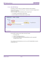
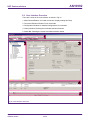
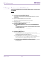
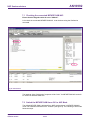
1
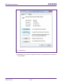
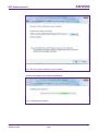
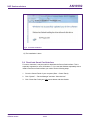
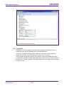
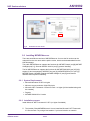
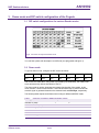
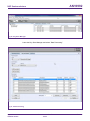
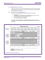
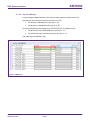
AN10992 Quick Startup Guide for RD710 Rev. 2.4 — 08 October 2012 198124 Application note COMPANY PUBLIC Document information Info Content Keywords RD710, Quick startup guide, SAM AV1, SAM AV2, RC523. Abstract This document is intended for new users to start working with the DesignIn Kit. It shows the basic functionality with MIFAREdiscover. AN10992 NXP Semiconductors Quick Startup Guide for RD710 Revision history Rev Date Description 2.4 20121008 Examples add and MIFARE discover explanation updated 2.3 20120807 Updated firmware info 2.2 20120710 FCC disclaimer, driver installer, Pegoda2Go, firmware info added, demo mode changed, outdated types removed, ISO replaced with ISO/IEC 2.1 20111206 Added in 5.1 the Activation of a MIFARE Classic Card. 2.0 20110803 Extended usecases for MIFAREdiscover 1.1 20110712 Update due to release of new usecases of MIFAREdiscover 1.0 20110411 Initial version 20110105 Draft version Contact information For more information, please visit: http://www.nxp.com For sales office addresses, please send an email to: [email protected] AN10992 Application note COMPANY PUBLIC All information provided in this document is subject to legal disclaimers. Rev. 2.4 — 08 October 2012 198124 © NXP B.V. 2012. All rights reserved. 2 of 68 AN10992 NXP Semiconductors Quick Startup Guide for RD710 1. Introduction The purpose of this document is to provide a set of guidelines to aid in the first operation of the RD710 reader. The MIFAREdiscover (ver.3.x.x) will be used as a user interface to communicate to the readers and cards, respectively. The USB drivers are included in the CD package and on NXP web (see [44]) 1.1 Firmware Info This package comes with a new firmware (version 2.2.7) for the RD710 reader. In this version the NXP Basic Function Library (BFL) is replaced by the NXP Reader Library (NXPRdLib). The functionality of the PC/SC mode has not been changed. The PC Software using the Reader in this mode (e.g. MIFAREDiscover) will not face any functional differences. 1.1.1 Additional functionality and benefits of Firmware v2.2.7 in standalone mode • Support of ISO/IEC 14443 Type B Tags • Improved multi Tag handling • Improved code structure and modular library design for easier development • Improved LPCXpresso Support For further information about the actual implementation please refer to [38]. 1.1.2 Firmware version installed on the Reader If you have received the reader together with this document version on CD it already contains the latest firmware. You can check this with the program Pegoda2Go which is as well in the CD package. If you have already installed the driver you can start Pegoda2Go as described in section 2.5 and check the current flashed version. Otherwise you have to install the drivers first. 1.1.3 Update Recommendation: For new projects and implementations the usage of the latest firmware and source code is recommended. This is as well the case for projects using the reader in PC/SC mode only. As the NXPRdLib has a different software design compared to the BFL, porting of existing projects based on the former firmware will require major rework and is not recommended unless one needs to take advantage of the additional functionality and benefits. If you want to flash to the latest version proceed as described in section 8. Therefore the latest binary file is located on the CD and on NXP web [42]. (Reader documentation\Cortex M3 \firmware_v2_2\pegoda_fw_v2_2.bin). AN10992 Application note COMPANY PUBLIC All information provided in this document is subject to legal disclaimers. Rev. 2.4 — 08 October 2012 198124 © NXP B.V. 2012. All rights reserved. 3 of 68 AN10992 NXP Semiconductors Quick Startup Guide for RD710 2. Installation 2.1 Required items To use the MIFAREdiscover, the following items are required: • MIFARE cards as MIFARE DESFire EV1, MIFARE Classic, MIFARE Ultralight • Pegoda Reader (RD710 or RD710 as part of EV710) (see [37]– [41]) • MIFAREdiscover o Public version available on NXP web (see [45]) o Full version (see [47]) 2.2 Installing USB driver for the Reader An installer for the USB drive is present on the CD (Driver\ Windows Driver Installer.exe). 1) Run this installer and follow the displayed instructions. 2) Connect the Pegoda RD710 with your computer. 3) Wait until Windows has installed the driver. If Windows installs the drives correctly you can skip section 2.3 and continue with section 2.4. 2.3 Installing USB driver for the Reader manually The demonstrated installation is shown on Windows 7, but it is the same in Windows XP and Vista. 4) If you don’t have a CD that was delivered with your Pegoda, open your web browser, go to see [44] and download and extract the zip file. 5) Connect the Pegoda RD710 with your computer. 6) Wait until Windows 7 installs a standard driver. 7) Open the Windows Device Manager and navigate to the installed Reader (see figure 1 below) AN10992 Application note COMPANY PUBLIC All information provided in this document is subject to legal disclaimers. Rev. 2.4 — 08 October 2012 198124 © NXP B.V. 2012. All rights reserved. 4 of 68 AN10992 NXP Semiconductors Quick Startup Guide for RD710 Fig 1. Device Manager 8) Click Smartcard Reader with the right mouse button and choose “Properties”. 9) Choose the tab driver and click “Update Driver”. AN10992 Application note COMPANY PUBLIC All information provided in this document is subject to legal disclaimers. Rev. 2.4 — 08 October 2012 198124 © NXP B.V. 2012. All rights reserved. 5 of 68 AN10992 NXP Semiconductors Quick Startup Guide for RD710 Fig 2. Update Driver 10) Windows will ask you how to search for the driver. Choose “Browse my computer for driver software”. AN10992 Application note COMPANY PUBLIC All information provided in this document is subject to legal disclaimers. Rev. 2.4 — 08 October 2012 198124 © NXP B.V. 2012. All rights reserved. 6 of 68 AN10992 NXP Semiconductors Quick Startup Guide for RD710 Fig 3. Browse Computer 11) Choose “Browse”, navigate to the root directory of the CD or the previous extracted content and click “Next”. AN10992 Application note COMPANY PUBLIC All information provided in this document is subject to legal disclaimers. Rev. 2.4 — 08 October 2012 198124 © NXP B.V. 2012. All rights reserved. 7 of 68 AN10992 NXP Semiconductors Quick Startup Guide for RD710 Fig 4. Browse for driver software on your computer 12) Wait until Windows has finished the installation. Fig 5. Installing driver software AN10992 Application note COMPANY PUBLIC All information provided in this document is subject to legal disclaimers. Rev. 2.4 — 08 October 2012 198124 © NXP B.V. 2012. All rights reserved. 8 of 68 AN10992 NXP Semiconductors Quick Startup Guide for RD710 Fig 6. Finished installation 13) The installation is done. 2.4 Deactivate Smart Card Interface For some customers it may be useful to deactivate the Smart Card Interface. This is especially important for users of Windows 7. If you see that Windows repeatedly tries to install a new Smart Card Interface you need to do the following steps. 1. Go to the Control Panel of your computer (Start – Control Panel) 2. Click “System” – “Device Manager” and then “Other devices” 3. Click “Smart Card” with your right mouse button and then disable. AN10992 Application note COMPANY PUBLIC All information provided in this document is subject to legal disclaimers. Rev. 2.4 — 08 October 2012 198124 © NXP B.V. 2012. All rights reserved. 9 of 68 AN10992 NXP Semiconductors Quick Startup Guide for RD710 Fig 7. Deactivate Smart Card Interface 2.5 Pegoda2Go Pegoda2Go is a small program to check the basic functions of the RD710. It can be started directly for the CD (\Software and Tools\Pegoda2GO.exe) If the driver is installed correctly and the Pegoda is connected the device should be present in the ‘Reader’ menu. May hitting the ‘Refresh’ item is required. Once the reader is selected the Action menu allows to switch the Antenna LEDs and to get information about the Pegoda configuration and the used firmware version as shown in figure Fig 8. If a card is present in the reader field the basic information of this card can be shown as well. AN10992 Application note COMPANY PUBLIC All information provided in this document is subject to legal disclaimers. Rev. 2.4 — 08 October 2012 198124 © NXP B.V. 2012. All rights reserved. 10 of 68 AN10992 NXP Semiconductors Quick Startup Guide for RD710 Fig 8. Firmware version check 2.6 Installing MIFAREdiscover There are two different versions of MIFAREdiscover; for once the full version can be retrieved from the doc store and the public version, which can be downloaded from the NXP Homepage. The public MIFAREdiscover supports the functions for MIFARE Classic (see[8]) MIFARE Ultralight (see[11]), General ISO/IEC 14443-A (see[7]) protocol handling. The full MIFAREdiscover supports the functions for MIFARE SAM AV2 (see [23]-[34]) support (X and conventional), MIFARE Plus (see [4]) MIFARE DESFire EV1 (see [3]), MIFARE Classic, MIFARE Ultralight, MIFARE Ultralight C (see [5]) and General ISO/IEC14443-A protocol handling. 2.6.1 System Requirements • Microsoft Windows XP SP2 or higher • Minimum screen resolution 1024x768 pixels • Microsoft .NET Framework 3.5 Service Pack 1 or higher [will be installed along with this installer] • Pegoda • MIFARE SAM AV2 for X-mode 2.6.2 Installation process Install Microsoft .NET Framework 3.5 SP1 (or higher if available) AN10992 Application note COMPANY PUBLIC The Installer "SetupMIFAREdiscover" tries to install the Microsoft .NET Framework 3.5 Service Pack 1 by using a Net-Installer. If you have limited or no network All information provided in this document is subject to legal disclaimers. Rev. 2.4 — 08 October 2012 198124 © NXP B.V. 2012. All rights reserved. 11 of 68 AN10992 NXP Semiconductors Quick Startup Guide for RD710 connection to download and install the Microsoft .NET Framework the setup process is terminated and you have to install the Microsoft .NET Framework manually. .NET Framework can be found online (see [48]) Install the "SetupMIFAREdiscover" package: Install the package and follow the instructions. The whole installation process requires administration rights. After you have successfully installed the program "MIFAREdiscover" and all of its required components you can start "MIFAREdiscover" via the link "Start -> All Programs -> NXP Semiconductors -> MIFAREdiscover -> MIFAREdiscover". AN10992 Application note COMPANY PUBLIC Read “ReleaseNotes.txt” file that you received with the MIFAREdiscover package. All information provided in this document is subject to legal disclaimers. Rev. 2.4 — 08 October 2012 198124 © NXP B.V. 2012. All rights reserved. 12 of 68 AN10992 NXP Semiconductors Quick Startup Guide for RD710 3. Demo mode and DIP switch configuration of the Pegoda 3.1 DIP switch configurations for various Reader modes Fig 9. Overview of important reader modi You can find a photo with description on NXP web (see [40]) (table and figure 1) 3.2 Demo mode To get into demo mode, configure the DIP switch as follows 8 7 6 5 4 3 2 1 OFF ON OFF OFF OFF OFF OFF OFF and connect the USB cable. Only power is provided by the USB cable, the reader itself works autonomously without interaction of the PC. The demo mode is used to showcase some basic functionality of the reader. In this mode, ISO/IEC 14443-3A and ISO/IEC 14443-3B activation loop is performed and an acoustic signal is generated based on the detected card and SAK-byte, respectively. The following table depicts the default sound coding for different MIFARE cards: Table 1. Card type according to SAK and number of beep Card Type beep blink AN10992 Application note COMPANY PUBLIC MIFARE 1K (0x08) 1 2 MIFARE Classic 4K (0x18) 2 2 MIFARE Ultralight (0x00) 3 2 MIFARE DESFire 4 2 MIFARE Plus 5 2 ISO/IEC 14443 Type B 1 1 All information provided in this document is subject to legal disclaimers. Rev. 2.4 — 08 October 2012 198124 © NXP B.V. 2012. All rights reserved. 13 of 68 AN10992 NXP Semiconductors Quick Startup Guide for RD710 If you still using the older firmware (v1.x) this demo mode behaves slightly different. There is no ISO/IEC 14443-3B activation loop and the reader reacts as described in the following table. Table 2. Card type according to SAK and number of beep for old firmware version Card Type Beep and blink MIFARE 1K (0x08) 1 MIFARE Classic 4K (0x18) 2 MIFARE Ultralight (0x00) 3 MIFARE DESFire 4 MIFARE Plus 5 This can be used to determine which firmware is currently running on the reader. AN10992 Application note COMPANY PUBLIC All information provided in this document is subject to legal disclaimers. Rev. 2.4 — 08 October 2012 198124 © NXP B.V. 2012. All rights reserved. 14 of 68 AN10992 NXP Semiconductors Quick Startup Guide for RD710 4. Public Version All in this section explained steps are applicable to the full version as well. 4.1 Starting MIFAREdiscover Connect the RD710 Reader with the PC by using the USB cable. Choose the desired DIP switch configuration on the mainboard of the reader (see chapter 3.1) as this tool does not support SAM. The DIP switches should all be set to “OFF”. Start MIFAREdiscover from the Start menu. Fig 10. Press the "get available Reader´s" button Press “Get available Reader’s” for the drop down field “contact- and contactless reader selection”. The available readers will be listed depending on the DIP switch configuration and the chosen reader. Press “Ok” to open the mainframe of the MIFAREdiscover program for the specific reader configuration. The following main window will appear. The History frame shows you that the reader has been opened successfully. The configured reader mode can be depicted from the history list as well. AN10992 Application note COMPANY PUBLIC All information provided in this document is subject to legal disclaimers. Rev. 2.4 — 08 October 2012 198124 © NXP B.V. 2012. All rights reserved. 15 of 68 AN10992 NXP Semiconductors Quick Startup Guide for RD710 4.2 Mainframe general overview The public MIFAREdiscover supports the functions for MIFARE Classic (see [9]), MIFARE Ultralight (see [11]), General ISO/IEC 14443-A (see [7]) protocol handling. Therefore, the user interface is divided into functional blocks which are shown in different tabs in Fig 11 (1). They open the so called ‘Command selection’ window (2) which allows to select a command window in (3). At the bottom (4) Fig 11 shows the history field where all the operations are displayed. For a more detailed view on the sent data and received data a switch to the log window is possible. Both fields can be cleared, or can be stored in a text file. 1. 3. 2. 4. Fig 11. Interface to Reader has been opened successfully Note: The sequence of commands as described in ISO/IEC 14443 or in the relevant datasheet must be kept to be able to activate and operate a card. The MIFAREdiscover does not cross check the logical command flow. AN10992 Application note COMPANY PUBLIC All information provided in this document is subject to legal disclaimers. Rev. 2.4 — 08 October 2012 198124 © NXP B.V. 2012. All rights reserved. 16 of 68 AN10992 NXP Semiconductors Quick Startup Guide for RD710 4.2.1 MIFARE Reader With this tab you can control the basic functions on the reader. Fig 12. MICORE 1,2 command window The “MICORE 1, 2’ command window allows you to reset the reader and to turn the electromagnetic (card reading) field off or on. The commands ‘ReadReg’ and ‘WriteReg’ allow reading or writing the register to control the reader. For further information on the register settings and functions please refer to the individual Reader ICs data sheet. Fig 13. Show Cards command window The ‘Show Cards’ command window in Fig 13 allows you to detect all the cards which are present in the reader field. With ‘Start Detection’ the reader starts to poll for cards (ISO 14443 Type A and B) and you get the UID of the cards presented to the Pegoda as well as the card type. With ‘Stop Detection’ the polling is stopped again. AN10992 Application note COMPANY PUBLIC All information provided in this document is subject to legal disclaimers. Rev. 2.4 — 08 October 2012 198124 © NXP B.V. 2012. All rights reserved. 17 of 68 AN10992 NXP Semiconductors Quick Startup Guide for RD710 4.2.2 MIFARE Classic The command window “ISO14443A Layer 3” is shown in Fig 14. 1. This part of the panel allows you to activate a number of cards and perform the anti-collision protocol according to [7] . The most convenient method is to push the ‘Activate Idle’ button. After that, in the table a UID appears in section 2 and its State is ‘Active’. 2. This section allows you to manage multiple cards in the reader field. Select a specific card you want to communicate with. Therefore this card has to be in ‘Active’ State. To to switch to another card in the reader field choose the current ‘Active’ card and with ‘Halt’ you can change the State from ‘Active’ to ‘Halt’ state (and work with another card in the meantime). Pick a ‘Halt’ UID and the button ‘Act.Wakeup’ changes the State back to ‘Active’ and you can work with the card again. ‘Clear List’ deletes all data in the table With the control elements it the blue section you can send individual commands and data to the card in an ISO 14443 Layer3 massage frame. Thereby the input format is hex coded. The checkboxes there indicate if you want to append a CRC code to the command and if you expect that the card to append a CRC to the response. The answer of the card is then displayed in the log windows. For a list of available command please refer to cards datasheet. 1. 2. 3. Fig 14. ISO14443A Layer 3 Fig 15 shows the ‘Data Processing’ window. With this window you can process the data stored on the MIFARE Classic card: AN10992 Application note COMPANY PUBLIC All information provided in this document is subject to legal disclaimers. Rev. 2.4 — 08 October 2012 198124 © NXP B.V. 2012. All rights reserved. 18 of 68 AN10992 NXP Semiconductors Quick Startup Guide for RD710 1. ‘Personalization UID Usage’ allows you to configure the type of UID the card should use. For the available types please refer to [8][8]. 2. To gain access to the different storage sectors of the card you first need to authenticate with a Key. Therefore you can choose a ‘BlockNo’ and the ‘Ref Key’ (prepared in the KeyStore 5.3.2.3) and use the button ‘MFC Auth Key A’ or ‘MFC Auth Key B’. 3. With ‘Read’ you can read a block from the card and with ‘Write’ you can write the block on the card then is selected in the data grid. Use ‘Increment’ to increase and ‘Decrement’ to decrease the contents of a block. The results are stored in an internal data-register. The ‘Restore’ button move the contents of a block into an internal data-register. Use ‘Transfer’ to write contents of the temporary internal data-register to a value block. 1. 2. 3. Fig 15. Data Processing 4.2.3 MIFARE Ultralight The Ultralight tab provides the ‘ISO14443A Layer 3’ command window as well. For the provide functionality please see section 4.2.2. The ‘Ultralight’ command window allows: 1. To read and write data on a chosen page of the card. 2. To write Lock Bytes (refer to [21]). AN10992 Application note COMPANY PUBLIC All information provided in this document is subject to legal disclaimers. Rev. 2.4 — 08 October 2012 198124 © NXP B.V. 2012. All rights reserved. 19 of 68 AN10992 NXP Semiconductors Quick Startup Guide for RD710 1. 2. Fig 16. UltralightC 4.2.4 MIFARE ISO14443A Layer 4 This tab provides all the functionality to work with ISO14443A Layer 4 [7] and the command window is shown in Fig 17. 1. This part can be use to activate a card to Layer 4 and control the date exchange rate. 2. The textbox shows the State of the cards. Control which card is the active one. 3. Use the blue marked part to send commands to the card in a ISO14443A Layer4 message frame format. For more information on the provided commands of this window please refer to [7]. 1. 2. 3. Fig 17. ISO14443A Layer 4 AN10992 Application note COMPANY PUBLIC All information provided in this document is subject to legal disclaimers. Rev. 2.4 — 08 October 2012 198124 © NXP B.V. 2012. All rights reserved. 20 of 68 AN10992 NXP Semiconductors Quick Startup Guide for RD710 4.2.5 Key Store Manager The Key Store Manager window as shown in Fig 18 allows you to define a number of Keys to be used for the authentication of e.g. memory sectors. Each key block can have a nickname and a certain type. It is divided in 3 keys, A B and C with individual Versions. From more information on keys and how to be used with cards please refer to the individual card IC datasheets. Fig 18. Key Store Manager AN10992 Application note COMPANY PUBLIC All information provided in this document is subject to legal disclaimers. Rev. 2.4 — 08 October 2012 198124 © NXP B.V. 2012. All rights reserved. 21 of 68 AN10992 NXP Semiconductors Quick Startup Guide for RD710 5. Example of some use case for the public version 5.1 Accessing the MIFARE Classic Open the ‘MIFARE Classic’ Tab and select ‘ISO 14443A Layer 3’. On the right side you can see a number of buttons for the activation of the card. The most convenient method is to push the ‘Activate Idle’ button. Then a UID appears in the table and the state changes to ‘Active’. Fig 19. Activate Idle Now open the Key Store Manager and select the following settings for the first Key: Key Type: MIFARE, Entry PartA: FFFFFFFFFFFF, Version: 0 as shown in Fig 20. AN10992 Application note COMPANY PUBLIC All information provided in this document is subject to legal disclaimers. Rev. 2.4 — 08 October 2012 198124 © NXP B.V. 2012. All rights reserved. 22 of 68 AN10992 NXP Semiconductors Quick Startup Guide for RD710 Fig 20. Key Store Manager Leave the Key Store Manager and select “Data Processing”. Fig 21. Data Processing AN10992 Application note COMPANY PUBLIC All information provided in this document is subject to legal disclaimers. Rev. 2.4 — 08 October 2012 198124 © NXP B.V. 2012. All rights reserved. 23 of 68 AN10992 NXP Semiconductors Quick Startup Guide for RD710 Select BlockNo 00, Ref Key 0, A and click "MFC Auth Key A" Now you should be able to read Sector 0 (Blocks 0-3). Select BlockNo 04, Ref Key 0, A and click "MFC Auth Key A" Now you should be able to read and write in Sector 1 (Blocks 4-7). The same is for all the other blocks and sectors. 5.2 Accessing the MIFARE Ultralight Open the ‘MIFARE Ultralight’ Tab and select ‘ISO 14443A Layer 3’. On the right side you can see a number of buttons for the activation of the card. The most convenient method is to push the ‘Activate Idle’ button. Then a UID appears in the table and the state changes to ‘Active’. Then select the “Ultralight” command window. Fig 22. Ultralight Select a ‘Page No’ and click ‘Read’ to read the data in the second text box. You also can write 4 Bytes into the first text box and click ‘Write’ to transfer it to the card. If you check the ‘Compatibility Write’ box you can write 16Byte at once (compatible to MIFARE Classic). The data is then distributed to 4 pages starting with the on selected at Page No. NOTE: Start writing at Block 3. The first three blocks (0 – 2) are reserved for the UID, some internal data and the lock bits of the memory. Keep in mind that you can only write when the lock bits (Block 2, Byte 2 and 3) are all set to 0b (read and write permission). AN10992 Application note COMPANY PUBLIC All information provided in this document is subject to legal disclaimers. Rev. 2.4 — 08 October 2012 198124 © NXP B.V. 2012. All rights reserved. 24 of 68 AN10992 NXP Semiconductors Quick Startup Guide for RD710 5.3 Writing NFC Tag MIFARE discover can be used to format MIFARE Card products to act a NFC Tags (refer to [17]) and store NDEF messages on them. The following examples show how to store an url in this format on the card to make it accessible from NFC devices. Therefore the NDEF Massage format is explained briefly. 5.3.1 The NDEF message A NDEF message is composed of one or more NDEF records as shown in figure Fig 23. Each Record has a Header and a Payload. The header is made of the Identifier, Length and Type. Fig 23. NDEF message The NDEF message use for the following examples should contain the url http://www.nxp.com. Therefore the coded message has to look as followed: 03 | 0C | D1| 01 08 55 01 6E 78 70 2E 63 6F 6D | FE The message starts with the Message TLV (Type Length Value) ‘03 0C D1’. 03 – NDEF Record (this byte defines the type of record) 0C – tells, how many bytes in the payload are D1 – Type of the record (first record? last record? short record? etc.) 01 – Type length (specifies the length of the Type field) 08 – Payload length, bytes that are used for the payload (01 6E 78 70 2E 63 6F 6D) 55 – Type field (‘55’ = ‘U’ and means URI) 01 – URI Identifier (‘http://www.’) 6E 78 70 2E 63 6F 6D - Payload, the rest of the string in hex-code (nxp.com) FE – Terminator TLV (‘Message is finished’) For details about the TLV refer to [22]. And if you want to read more information about creating a NDEF Message, please refer to [19]. AN10992 Application note COMPANY PUBLIC All information provided in this document is subject to legal disclaimers. Rev. 2.4 — 08 October 2012 198124 © NXP B.V. 2012. All rights reserved. 25 of 68 AN10992 NXP Semiconductors Quick Startup Guide for RD710 5.3.2 MIFARE Classic as NFC Tag This part now shows how you can use the MIFARE Classic as NFC Tag [16] and put a NDEF message on a blank Card. We use the previously explained message url NDEF massage and store it on the Card. 5.3.2.1 Default factory settings MIFARE Classic First there is some informative data about a MIFARE Classic Card [8][8]. • • • • • 16 Sectors (0 – 15) Standard Key A = FFFFFFFFFFFF and standard Key B = FFFFFFFFFFFF Access bits are set to ‘FF0780’ and the GPB is ‘69’ You can read and write only with Key A You cannot write in Block 0 of Sector 0 Every Sector contains 4 Blocks (0 – 3). Block 3 is always the Sector Trailer which contains Key A, the Access Bits, GPB and Key B of the Sector. Block 0, 1 and 2 are for storing data. Fig 24. MIFARE Classic - Memory organization AN10992 Application note COMPANY PUBLIC All information provided in this document is subject to legal disclaimers. Rev. 2.4 — 08 October 2012 198124 © NXP B.V. 2012. All rights reserved. 26 of 68 AN10992 NXP Semiconductors Quick Startup Guide for RD710 The only exception is Sector 0. Block 0 is read-only and contains the UID. The first two bytes of Block 1 are for the CRC byte (cyclic redundancy check) and the Info byte. There are 30 bytes remaining in Block 1 and 2. These are splitted in groups of two. Every bytepair represents one Sector, starting at 1 and ending with 15. Further Information can be found there: [16] 5.3.2.2 Activate the Card Use the MIFARE Classic Tab and push the ‘Activate Idle’ button to communicate with the current card. Fig 25. Push ‘ActivateIdle’ AN10992 Application note COMPANY PUBLIC All information provided in this document is subject to legal disclaimers. Rev. 2.4 — 08 October 2012 198124 © NXP B.V. 2012. All rights reserved. 27 of 68 AN10992 NXP Semiconductors Quick Startup Guide for RD710 5.3.2.3 Key Store Manager For accessing the different blocks of the card you have prepare a certain set of keys. Open the key store and put in the keys as shown in Fig 26. • The red Key is standard Key A (‘Key No: 0, A’). • The blue Key is standard Key B (‘Key No: 0, B’). All keys (=standard key) are always set to FFFFFFFFFFFF, as explained in [8]. • The green Key is the public MAD Key A (‘Key No: 1, A’). • The yellow Key is the public Sector Key A (‘Key No: 2, A’). The public keys are defined in [16]. Fig 26. Set MAD Keys AN10992 Application note COMPANY PUBLIC All information provided in this document is subject to legal disclaimers. Rev. 2.4 — 08 October 2012 198124 © NXP B.V. 2012. All rights reserved. 28 of 68 AN10992 NXP Semiconductors Quick Startup Guide for RD710 5.3.2.4 Formatting the MIFARE Classic to NFC Tag The make the Information accessible by an NFC device as certain data structure has to be set in place. The first step is to set the Keys of the MAD Keys, therefore: 1. To Authenticate for Block 00-03 select BlockNo 00 and standard Key A (Key No: 0, A) and push ‘MFC Auth Key A’ 2. Write ‘A0A1A2A3A4A5787788C1FFFFFFFFFFFF’ to Block 03 and push ‘Write’ Note: The orange and green highlighted parts are Key A and Key B. The lavender highlighted parts are the Access bits. In this case they stand for read-only with Key A and read and write access with Key B. The yellow highlighted part is the GPB (General Purpose Bit). More information on the coding of these bits can be found in [20]. 1. 2. Fig 27. Set MAD Keys AN10992 Application note COMPANY PUBLIC All information provided in this document is subject to legal disclaimers. Rev. 2.4 — 08 October 2012 198124 © NXP B.V. 2012. All rights reserved. 29 of 68 AN10992 NXP Semiconductors Quick Startup Guide for RD710 Now the information where to find the NDEF massage in the card storage has to be written into the MAD: 1. To authenticate for block 00 to 03 select BlockNo 00 and Key B and push ‘MFC Auth Key B’ 2. Write ‘ C00103E1000000000000000000000000’ to Block 01 and push ‘Write’ ‘03E1’ is the NFC AID [22]. C001 contains the CRC and Info – Byte according to [20]. Now you can use Sector 1 of the MIFARE Classic Card to write your NDEF message. 1. 2. 3. Fig 28. Set MAD AN10992 Application note COMPANY PUBLIC All information provided in this document is subject to legal disclaimers. Rev. 2.4 — 08 October 2012 198124 © NXP B.V. 2012. All rights reserved. 30 of 68 AN10992 NXP Semiconductors Quick Startup Guide for RD710 Next the Sector Keys and Access rights for this sector have to be set: 3. To authenticate for block 04 to 07 select Block 04 and standard Key A (Key No: 0, A) and push ‘MFC Auth Key A’ 4. Write ‘D3F7D3F7D3F77F078840FFFFFFFFFFFF’ to Block 07 and push ‘Write’ In this case the Access bits 7F0788 stand for read and write access with Key A and B. 1. 2. 3. Fig 29. Set Sector Keys AN10992 Application note COMPANY PUBLIC All information provided in this document is subject to legal disclaimers. Rev. 2.4 — 08 October 2012 198124 © NXP B.V. 2012. All rights reserved. 31 of 68 AN10992 NXP Semiconductors Quick Startup Guide for RD710 5.3.2.5 Write NDEF Message Last step is to write the actual NDEF message to the card. 1. Authenticate with BlockNo 04 with Key A (Key No: 2, A) and push ‘MFC Auth Key A’ 2. Write ‘030CD1010855016E78702E636F6DFE00’ (see 5.3.1) to Block 04 and 1. 2. Fig 30. Write NDEF message push ‘Write’ The procedure is now finished and you can use e.g. a NFC enabled Mobile to test the configured NFC Tag. AN10992 Application note COMPANY PUBLIC All information provided in this document is subject to legal disclaimers. Rev. 2.4 — 08 October 2012 198124 © NXP B.V. 2012. All rights reserved. 32 of 68 AN10992 NXP Semiconductors Quick Startup Guide for RD710 5.3.3 MIFARE Ultralight as NFC Tag This is a short explanation how to use the MIFARE Ultralight as an NFC Tag Type 2 [21] store an NDEF message on the card. The used masseag contains the URL: http://www.nxp.com. 5.3.3.1 Default factory settings MIFARE Ultralight The first three pages (00 – 02) are used for the UID, some internal data and the lock bits of the memory. They are read-only. Therefore you start writing at Page 03. Page 03 is only ‘one time programmable’. Fig 31. Memory of a Ultralight card Every page is made of 4 bytes. On page 02 Byte 2 and 3 need to be set to ’00 00’, else you cannot write or read. For details refer to [21]. 5.3.3.2 Activate TAG To activate the Card use the MIFARE Ultralight Tab and push the ‘Activate Idle’ button as shown in Fig 25. AN10992 Application note COMPANY PUBLIC All information provided in this document is subject to legal disclaimers. Rev. 2.4 — 08 October 2012 198124 © NXP B.V. 2012. All rights reserved. 33 of 68 AN10992 NXP Semiconductors Quick Startup Guide for RD710 5.3.3.3 Write NDEF Message First step is to set the so called CC (Capability Container) located at page 03. Please NOTE that once you set a bit to logic 1 in this area, it cannot be changed back to 0 anymore (xor operation). Select the ‘Ultralight’ command window as shown in figure Fig 32. 1. Pick ‘Page No’ 03 and press the ‘Read’ button. 2. Write ‘E1100600’ into the Data textbox and push ‘Write’. 2. 1. Fig 32. Set the CC Now the NDEF message can be written to the tag. Therefore: 1. Pick ‘Page No’ 04 2. tackle the ‘Compatibility Write’ box 3. Write ‘030CD1010855016E78702E636F6DFE00’ (the HEX coded NDEF message) and click ‘Write’ The procedure is now finished and you can use e.g. a NFC enabled Mobile to test the configured NFC Tag. AN10992 Application note COMPANY PUBLIC All information provided in this document is subject to legal disclaimers. Rev. 2.4 — 08 October 2012 198124 © NXP B.V. 2012. All rights reserved. 34 of 68 AN10992 NXP Semiconductors Quick Startup Guide for RD710 6. Full Version 6.1 Starting MIFAREdiscover Connect RD710 Reader to the PC with USB cable. Choose the desired DIP switch configuration on the mainboard of the reader (see figure 9). This can be • Reader in X-Mode for RD710 with MIFARE SAM inserted in the slot • Reader in No SAM-Mode • Reader in S-Mode In the following descriptions we need to have the DIP switch of the Pegoda set to XMode. Start MIFAREdiscover from the Start menu. You will be asked to select your reader connected to MIFARE AV2 SAM as shown in Fig.15. Fig 33. Select reader connected to SAM Select the reader. Any time the profile can be closed or opened by using close and open profile respectively. After selection of the reader the key file can be browsed if it is necessary. In the key file, the secret keys can be stored, which may be needed to authenticate MIFARE SAM AV2 with the host or to be changed later. Press OK button to validate the profile. If the MIFARE SAM AV2 is connected properly, the status field of the history window shows “SUCCESS”. AN10992 Application note COMPANY PUBLIC All information provided in this document is subject to legal disclaimers. Rev. 2.4 — 08 October 2012 198124 © NXP B.V. 2012. All rights reserved. 35 of 68 AN10992 NXP Semiconductors Quick Startup Guide for RD710 6.2 User Interface Overview There are 5 areas in the main window, as shown in Fig 16. 1. Menu Bar and Buttons: for reader connection, display settings and help 2. Command Selection Window: list of commands 3. Configuration Window: for detailed configurations of commands 4. History Window: Showing the command execution histories 5. Status Bar: Showing the current command execution status Fig 34. User Interface Overview AN10992 Application note COMPANY PUBLIC All information provided in this document is subject to legal disclaimers. Rev. 2.4 — 08 October 2012 198124 © NXP B.V. 2012. All rights reserved. 36 of 68 AN10992 NXP Semiconductors Quick Startup Guide for RD710 7. Examples of some use cases for the full version In every use case (defined below) we need to have the DIP switch of the Pegoda reader set to X-Mode. Overview 7.1. Checking the connected MIFARE SAM AV2 Here you will get some hardware and software related information about the installed SAM. 7.2. Switch the MIFARE SAM from AV1 to AV2 Mode AV2 mode is recommended because of security reasons. 7.3. Authenticate host This step is needed when operating with the SAM. 7.4. Operating the MIFARE DESFire EV1 7.4.1.Using MIFARE SAM AV2 for communication with MIFARE DESFire EV1 This example shows how to perform a basic authentication between SAM and MIFARE DESFire EV1. 7.4.2.Create Application and format MIFARE DESFire 7.4.3.Authenticate Application 7.5. Operating the MIFARE Plus S 7.5.1.Switch MIFARE Plus from Security Level 0 in Security Level 1 Security level 0 is the initial delivery configuration of the PICC. We have to pre-personalize the card to get into security level 1. 7.5.2.Switch MIFARE Plus from Security Level 1 in Security Level 3 Because security level 1 is the compatibility mode to the MIFARE Classic card, we want to use the enhanced security of security level 3. 7.5.3.Read/Write Actions of MIFARE Plus in Security Level 3 A short introduction of how to access blocks with read and write operation in security level 3. AN10992 Application note COMPANY PUBLIC All information provided in this document is subject to legal disclaimers. Rev. 2.4 — 08 October 2012 198124 © NXP B.V. 2012. All rights reserved. 37 of 68 AN10992 NXP Semiconductors Quick Startup Guide for RD710 7.1 Checking the connected MIFARE SAM AV2 Ensure that the Pegoda reader is set to “X-Mode”. Let’s check the connected MIFARE SAM AV2. It can be done using the GetVersion command. Fig 35. Get Version The last byte of the “GetVersion” response will be “0xA1” for MIFARE SAM AV1 and will be “0xA2” for MIFARE SAM AV2. 7.2 Switch the MIFARE SAM from AV1 to AV2 Mode The default MIFARE SAM is delivered from NXP semiconductor in MIFARE SAM AV1 mode. DIP switches should be set to “X-Mode” (see figure 9). For switching to AV2 mode follow the steps. AN10992 Application note COMPANY PUBLIC All information provided in this document is subject to legal disclaimers. Rev. 2.4 — 08 October 2012 198124 © NXP B.V. 2012. All rights reserved. 38 of 68 AN10992 NXP Semiconductors Quick Startup Guide for RD710 7.2.1 Authenticate host Select the “AuthenticateHost” command at the command window. Set the reference key as shown in the following figure. The reference key here used is “Key No: 0, A” for the default setting, where you need to authenticate host using SAM Master key entry and version “00” to change the key. Fig 36. AuthenticateHost Key AN10992 Application note COMPANY PUBLIC All information provided in this document is subject to legal disclaimers. Rev. 2.4 — 08 October 2012 198124 © NXP B.V. 2012. All rights reserved. 39 of 68 AN10992 NXP Semiconductors Quick Startup Guide for RD710 7.2.2 Change SAM Master key to AES SAM master key entry has to be changed to AES type to be able to switch the SAM mode. Select the “KeyEntryManagement” Command from the command window and set the key “00” and key type “AES 128” (AES 192 is also ok). Set other field as shown in the following figure. We take the new key values and version all 00s, if you want, you can make your own keys as you like. Fig 37. Change SAM master key to AES AN10992 Application note COMPANY PUBLIC All information provided in this document is subject to legal disclaimers. Rev. 2.4 — 08 October 2012 198124 © NXP B.V. 2012. All rights reserved. 40 of 68 AN10992 NXP Semiconductors Quick Startup Guide for RD710 If the SAM master key is already AES key type the steps 7.2.1 and 7.2.2 are not required. Now change the key entry in the key file to have the same key as we have in the MIFARE SAM. Open the key file from menu. Change the key type and key values as we downloaded in previous command. Fig 38. Change Key Type 7.2.3 Lock/Unlock Command Now the MIFARE SAM AV2 is ready to accept the Activation of AV2 mode command. Select the “Lock/Unlock” Command from the command window. Set the mode to “Activate AV2 mode” and refer to the key “key no: 0, A” of the key file as shown in the following figure, figure 21. Fig 39. Lock/Unlock command AN10992 Application note COMPANY PUBLIC All information provided in this document is subject to legal disclaimers. Rev. 2.4 — 08 October 2012 198124 © NXP B.V. 2012. All rights reserved. 41 of 68 AN10992 NXP Semiconductors Quick Startup Guide for RD710 Now the MIFARE SAM is switched to AV2 mode. AN10992 Application note COMPANY PUBLIC All information provided in this document is subject to legal disclaimers. Rev. 2.4 — 08 October 2012 198124 © NXP B.V. 2012. All rights reserved. 42 of 68 AN10992 NXP Semiconductors Quick Startup Guide for RD710 7.3 Authenticate Host Ensure that the Pegoda reader is set to “X-Mode”. Select the “AuthenticateHost” command at the command window and open the Key Store Manager. Fig 40. Key Store Manager Change the settings: KeyNo: 0, Key Type: AES 128, Part A: 0000000000000000000, VersionA: 00 Fig 41. Change Key Type Leave the Key Store manager and select “AuthenticateHost” again. Be sure to tick “Generate session key” at the AuthMode section and “Plain” at HostMode. Click “AuthHost”. AN10992 Application note COMPANY PUBLIC All information provided in this document is subject to legal disclaimers. Rev. 2.4 — 08 October 2012 198124 © NXP B.V. 2012. All rights reserved. 43 of 68 AN10992 NXP Semiconductors Quick Startup Guide for RD710 Fig 42. AuthHost 7.4 Operating the MIFARE DESFire EV1 The MIFARE DESFire EV1 answers every command with a status code. These codes can be found in MIFAREdiscover command selection at the Received data column. For example, if you enter an invalid command you will get “AppDataOut=0x1C”. A list with useful status and error codes is provided: Table 3. Useful status and error codes Hex Code Status AN10992 Application note COMPANY PUBLIC 0x00 OPERATION_OK 0x0C NO_CHANGES 0x0E OUT_OF_EEPROM_ERROR 0x1C ILLEGAL_COMMAND_CODE 0x1E INTEGRITY_ERROR 0x40 NO_SUCH_KEY 0x7E LENGTH_ERROR 0x9D PERMISSION_DENIED 0x9E PARAMETER_ERROR 0xA0 APPLICATION_NOT_FOUND 0xA1 APPL_INTEGRITY_ERROR 0xAE AUTHENTICATION_ERROR 0xAF ADDITIONAL_FRAME 0xBE BOUNDARY_ERROR All information provided in this document is subject to legal disclaimers. Rev. 2.4 — 08 October 2012 198124 © NXP B.V. 2012. All rights reserved. 44 of 68 AN10992 NXP Semiconductors Quick Startup Guide for RD710 Hex Code Status 0xC1 PICC_INTEGRITY_ERROR 0xCD PICC_DISABLED_ERROR 0xCE COUNT_ERROR 0xDE DUPLICATE_ERROR 0xEE EEPROM_ERROR 0xF0 FILE_NOT_FOUND 0xF1 FILE_INTEGRITY_ERROR 7.4.1 Using MIFARE SAM AV2 for communication with MIFARE DESFire EV1 At first, the DESFire Key has to be downloaded to the MIFARE SAM if it is not already there. According to the steps done here, downloading a key to the MIFARE SAM requires host authentication as shown in § 7.3. 7.4.1.1 Uploading MIFARE DESFire EV1 AES key to SAM Let’s change the key entry number 1 to PICC DESFire EV1 AES key. To make it simple Key A = “00000000000000000000000000000000”, version 0x00 Key B = “11111111111111111111111111111111”, version 0x01 Key C = “22222222222222222222222222222222”, version 0x02 The other options are checked as shown in the following figure, figure 25. Fig 43. Downloading MIFARE DESFire EV1 AES key to SAM Do not forget to tick the “keep Init Vector” option for DESFire EV1 AES and standard TDEA keys. AN10992 Application note COMPANY PUBLIC All information provided in this document is subject to legal disclaimers. Rev. 2.4 — 08 October 2012 198124 © NXP B.V. 2012. All rights reserved. 45 of 68 AN10992 NXP Semiconductors Quick Startup Guide for RD710 7.4.1.2 Accessing MIFARE DESFire EV1 The steps are as follows: 2 1. RC Init to initialize the I C communication (shown in fig. 26). 2. RC RFControl to turn on the RF field (shown in fig. 26). 1 2 Fig 44. RC Init and RC RF Control 3. ActivateIdle to activate the MIFARE DESFire EV1 card to ISO/IEC14443 part 3 (shown in fig. 27). 4. RATS and PPS command to prepare the MIFARE DESFire EV1 card to ISO/IEC 14443-4 layer (shown in fig. 28). AN10992 Application note COMPANY PUBLIC All information provided in this document is subject to legal disclaimers. Rev. 2.4 — 08 October 2012 198124 © NXP B.V. 2012. All rights reserved. 46 of 68 AN10992 NXP Semiconductors Quick Startup Guide for RD710 3 Fig 45. ActivateIdle AN10992 Application note COMPANY PUBLIC All information provided in this document is subject to legal disclaimers. Rev. 2.4 — 08 October 2012 198124 © NXP B.V. 2012. All rights reserved. 47 of 68 AN10992 NXP Semiconductors Quick Startup Guide for RD710 4 Fig 46. RATS + PPS Sometimes, when opening RD710 with MIFARE SAM AV2 for the first time, ReqA and ActivateIdle commands fail. As a workaround, please execute the following steps. Select “SAM Configuration” and “Exchange” at the Command Selection window and insert the following data: CLA = 0x80, INS = 0x2E, P1 = 0x00, P2 = 0x00, Lc = 0x16 Tick „Use Data“ Data: 2A822BAA15401875194D265927F4283F29110C100100 And press “Exchange”. Fig 47. Exchange Data AN10992 Application note COMPANY PUBLIC All information provided in this document is subject to legal disclaimers. Rev. 2.4 — 08 October 2012 198124 © NXP B.V. 2012. All rights reserved. 48 of 68 AN10992 NXP Semiconductors Quick Startup Guide for RD710 7.4.2 Create Application and format MIFARE DESFire 1. See § 7.3 and do the AuthenticateHost command 2. Open the “KeyEntryManagement” and change the Master Key to KeyNo: 03 if it is still “default”. The Key Type has to be TDEA – DESFire. All Keys and Versions are 0, KeyClass is PICC. Be sure to tick everything at Programming bit mask (see figure below). Fig 48. ChangeKeyEntry 3. Click “ChangeKeyEntry” 2. To get access to DESFire, do the steps described in § 7.4.1.2. 3. Then select “X-DESFire Data Processing” at the Command Selection and insert the following data: DESFire KeyNo:0 “Selection by key entry number” Mode: Native Current Key KeyNo: 0x03, KeyVersion 0x00 4. Click “AuthPICC”. AN10992 Application note COMPANY PUBLIC All information provided in this document is subject to legal disclaimers. Rev. 2.4 — 08 October 2012 198124 © NXP B.V. 2012. All rights reserved. 49 of 68 AN10992 NXP Semiconductors Quick Startup Guide for RD710 Fig 49. AuthPICC 5. Go to “ISO14443A-4”. 6. To see applications on the card, insert “0x6A” and click “Exchange”. To create a new application, insert “0xCaaaaaaa0f8e” and click “Exchange” (The repeated “a” describe the AID (Application ID)) To format the card, insert “0xfc” and click “Exchange”. AN10992 Application note COMPANY PUBLIC All information provided in this document is subject to legal disclaimers. Rev. 2.4 — 08 October 2012 198124 © NXP B.V. 2012. All rights reserved. 50 of 68 AN10992 NXP Semiconductors Quick Startup Guide for RD710 7.4.3 Authenticate Application 1. Do the ApplicationHost command, as described in § 7.3. 2. Open the “KeyEntryManagement” and change the Master Key to “KeyNo: 01” if it is still “default”. The Key Type has to be AES 128. All Keys and Versions are 0, KeyClass is PICC. Be sure to tick everything at Programming bit mask and “Keep Init Vector (DESFire)”. 3. Click “ChangeKeyEntry” 4. To get access to DESFire, do the steps described in § 7.4.2. 5. Select Application with “5aaaaaaa” and click “Exchange”. Fig 50. Select Application 6. Select “X-DESFire Data Processing” at the Command Selection 7. Insert the following data: DESFire KeyNo: 1 "Selection by key entry number” Mode: Native Current Key: Key No.: 01, Key Version: 0 AN10992 Application note COMPANY PUBLIC All information provided in this document is subject to legal disclaimers. Rev. 2.4 — 08 October 2012 198124 © NXP B.V. 2012. All rights reserved. 51 of 68 AN10992 NXP Semiconductors Quick Startup Guide for RD710 8. Click “AuthPICC”. Now you are registered with your first Application. 7.5 Operating the MIFARE Plus S To get to MIFARE Plus, you have to set the DIP switches to X-mode (see figure 9) and switch the MIFARE SAM into AV2 mode. 7.5.1 Switch MIFARE Plus from Security Level 0 in Security Level 1 Select “MIFARE Plus” (below the Menu bar) and then “ISO14443A Layer 3” at the command selection. Click “RF Reset” first and “Activate Idle” afterwards. Fig 51. RF Reset and ActivateIdle Go to “ISO14443A Layer 4” and click “ActivateCard”. AN10992 Application note COMPANY PUBLIC All information provided in this document is subject to legal disclaimers. Rev. 2.4 — 08 October 2012 198124 © NXP B.V. 2012. All rights reserved. 52 of 68 AN10992 NXP Semiconductors Quick Startup Guide for RD710 Fig 52. Activate Card AN10992 Application note COMPANY PUBLIC All information provided in this document is subject to legal disclaimers. Rev. 2.4 — 08 October 2012 198124 © NXP B.V. 2012. All rights reserved. 53 of 68 AN10992 NXP Semiconductors Quick Startup Guide for RD710 Select “Security Level 0” at the Command selection and insert the data as the next figure shows: Fig 53. Switch into Security Level 1 Press Ctrl on your keyboard to select all 3 entries. Then click “Write Perso” and afterwards “Commit Perso”. Then, press the following buttons (Menu bar) in this sequence: "RF Reset", "ActivateIdle", "ActivateCard". Now, your card is in Security Level 1. AN10992 Application note COMPANY PUBLIC All information provided in this document is subject to legal disclaimers. Rev. 2.4 — 08 October 2012 198124 © NXP B.V. 2012. All rights reserved. 54 of 68 AN10992 NXP Semiconductors Quick Startup Guide for RD710 7.5.2 Switch MIFARE Plus from Security Level 1 in Security Level 3 After switching MIFARE Plus into Security Level 1, it is now possible to switch to Security Level 3. Select “Security Level 1” at the Command selection and change the settings as shown in the following figure. Click “FirstAuth” after you are done. Fig 54. Switch into Security Level 3 Now your card is in Security Level 3. You can check if the MIFARE Plus is in security level 3 by performing an “ActivateIdle” command. At the section “Received Data” in the command history you will see the SAK of the card afterwards. For example, if you have a 4KB MIFARE Plus card you will get 0x20 if it is in Security Level 3. See the Application note AN10833 for details. (http://www.nxp.com/documents/application_note/AN10833.pdf) AN10992 Application note COMPANY PUBLIC All information provided in this document is subject to legal disclaimers. Rev. 2.4 — 08 October 2012 198124 © NXP B.V. 2012. All rights reserved. 55 of 68 AN10992 NXP Semiconductors Quick Startup Guide for RD710 7.5.3 Read/Write Actions of MIFARE Plus in Security Level 3 Select “Security Level 3” at the Command selection. Because the standard key for the blocks are the same as we inserted at the keystore at position 02, version 02, we can now use these to authenticate at different storage locations. Change the settings: Block/KeyNo: 4000 Ref Key No: 02 Ref Key Version: 02 “HW – KeyStore” And click “FirstAuth” If you click “Read” you can now read the individual blocks and if you click “Write” you can write beforehand edited blocks. Be sure to tick “MAC on Command” and “MAC on Response” (figure 37). Fig 55. Read/Write Actions AN10992 Application note COMPANY PUBLIC All information provided in this document is subject to legal disclaimers. Rev. 2.4 — 08 October 2012 198124 © NXP B.V. 2012. All rights reserved. 56 of 68 AN10992 NXP Semiconductors Quick Startup Guide for RD710 7.6 Using MIFAREdiscover without MIFARE SAM AV2 Ensure that the Pegoda is set to „Normal Mode“. All described accesses to MIFARE cards are also possible without the MIFARE SAM AV2. If you use a MIFARE SAM AV2 all keys that are needed to get access to MIFARE cards get stored on the SAM. If no MIFARE SAM AV2 is used the keys have to be inserted at the Key Store Manager of MIFAREdiscover. At positions where a key is needed you have to insert “SW – KeyStore” and the suitable storage location instead of “HWKeyStore”. AN10992 Application note COMPANY PUBLIC All information provided in this document is subject to legal disclaimers. Rev. 2.4 — 08 October 2012 198124 © NXP B.V. 2012. All rights reserved. 57 of 68 AN10992 NXP Semiconductors Quick Startup Guide for RD710 8. Firmware download In order to download firmware to the reader, the DIP switches have to be configured to “flash mode” as described in section 3. After a reset of the Pegoda reader it does response as mass storage device. The user can upgrade the Pegoda firmware by copying it (drag and drop) to the Pegoda mass storage device. Important note: The file name of the binary file must be renamed to pegoda2x.bin, where x can be any character or letter or none; otherwise the Pegoda will refuse to copy the file and Windows will response with an I/O error (see 36). Fig 56. I/O Error when filename is not correct After successfully copying the file, the Pegoda will start blinking and beeping; windows will response with the following message (see 37). Don’t be irritated that this is a windows error dialog as well. Fig 57. Firmware download successful Now, the firmware has been updated; reset the device and choose the desired reader mode with the DIP switches. AN10992 Application note COMPANY PUBLIC All information provided in this document is subject to legal disclaimers. Rev. 2.4 — 08 October 2012 198124 © NXP B.V. 2012. All rights reserved. 58 of 68 AN10992 NXP Semiconductors Quick Startup Guide for RD710 9. Error Codes In MIFAREdiscover, user will observe following error and component codes in the History window under Status Info. The definitions of the error codes will help user to understand the cause of error. Error codes & definitions Error Codes Definition SUCCESS Returned in case of no error SUCCESS_CHAINING Rx chaining is not complete, further action needed SUCCESS_INCOMPLETE_BYTE An incomplete byte was received AN10992 Application note COMPANY PUBLIC IO_TIMEOUT No reply received, e.g. PICC removal INTEGRITY_ERROR Wrong CRC or parity detected COLLISION_ERROR A collision occurred BUFFER_OVERFLOW Attempt to write beyond buffer size FRAMING_ERROR Invalid frame format PROTOCOL_ERROR Received response violates protocol AUTH_ERROR Authentication error READ_WRITE_ERROR A Read or Write error occurred in RAM/ROM or Flash TEMPERATURE_ERROR The RC sensors signal overheating RF_ERROR Error on RF-Interface INTERFACE_ERROR An error occurred in RC communication LENGTH_ERROR A length error occurred INTERNAL_ERROR An internal error occurred INVALID_DATA_PARAMS failed) Invalid data parameters supplied (layer id check INVALID_PARAMETER Invalid parameter supplied PARAMETER_OVERFLOW overflow Reading/Writing a parameter would produce an UNSUPPORTED_PARAMETER Parameter not supported UNSUPPORTED_COMMAND Command not supported USE_CONDITION Condition of use not satisfied KEY A key error occurred All information provided in this document is subject to legal disclaimers. Rev. 2.4 — 08 October 2012 198124 © NXP B.V. 2012. All rights reserved. 59 of 68 AN10992 NXP Semiconductors Quick Startup Guide for RD710 Component codes & Identifiers AN10992 Application note COMPANY PUBLIC Component Code Identifiers GENERIC Generic Component Code BAL BAL Component Code HAL HAL Component Code PAL_ISO14443P3A ISO14443-3A PAL-Component Code PAL_ISO14443P3B ISO14443-3B PAL-Component Code PAL_ISO14443P4A ISO14443-4A PAL-Component Code PAL_ISO14443P4 ISO14443-4 PAL-Component Code PAL_MIFARE MIFARE(R) PAL-Component Code PAL_FELICA Open FeliCa PAL-Component Code PAL_EPCUID ICode EPC/UID PAL-Component Code PAL_SLI15693 ICode SLI/ISO15693 PAL-Component Code PAL_I18000P3M3 ISO18000-3 Mode3 PAL-Component Code PAL_I18092MPI Code ISO18092 passive initiator mode PAL-Component AL_MFC MIFARE(R) Classic AL-Component Code AL_MFUL MIFARE(R) Ultralight AL-Component Code AL_MFP MIFARE(R) Plus AL-Component Code AL_VCA Virtual Card Architecture AL-Component Code AL_FELICA Open FeliCa AL-Component Code AL_I15693 ISO15693 AL-Component Code AL_SLI ICode SLI AL-Component Code AL_I18000P3M3 ISO18000-3 Mode3 AL-Component Code AL_MFDF MIFARE DESFIRE EV1 AL Component Code AL_P40CMDPRIV P40 command libraryAL-Component Code AL_P40CMDPUB P40 command libraryAL-Component Code DL_AMP Amplifier DL-Component Code DL_THSTRM Thermostream DL-Component Code DL_OSCI Oscilloscope DL-Component Code DL_RDFPGA Reader FPGA Box DL-Component Code DL_MSTAMPOSC Master Amplifier Oscilloscope DL-Component Code DL_STEPPER Stepper DL-Component Code CIDMANAGER Cid Manager Component Code CRYPTOSYM CryptoSym Component Code KEYSTORE KeyStore Component Code All information provided in this document is subject to legal disclaimers. Rev. 2.4 — 08 October 2012 198124 © NXP B.V. 2012. All rights reserved. 60 of 68 AN10992 NXP Semiconductors Quick Startup Guide for RD710 AN10992 Application note COMPANY PUBLIC TOOLS Tools Component Code CRYPTORNG CryptoRng Component Code LOG Log Component Code All information provided in this document is subject to legal disclaimers. Rev. 2.4 — 08 October 2012 198124 © NXP B.V. 2012. All rights reserved. 61 of 68 AN10992 NXP Semiconductors Quick Startup Guide for RD710 10. References AN10992 Application note COMPANY PUBLIC 1) [1] Datasheet – MFR523; Contactless reader IC, BU-ID Doc. No. 1152** , available on NXP Web: http://www.nxp.com/documents/data_sheet/MFRC523.pdf [2] Datasheet – MFEV710, Pegoda EV710, available on NXP Web: http://www.nxp.com/documents/short_data_sheet/MFEV710_SDS.pdf [3] Datasheet – MIFARE DESFire; MF3ICDx21_41_81, MIFARE DESFire EV1 contactless multi-application IC, BU-ID Doc. No. 1340**, available on NXP docu control [4] Datasheet – MIFARE Plus; MF1PLUSx0y1, Mainstream contactless smart card IC for fast and easy solution development, BU-ID Doc. No. 163734, available at NXP docu control http://www.nxp.com/documents/short_data_sheet/MF1PLUSX0Y1_SDS.pdf [5] Datasheet – MIFARE Ultralight C; MF0ICU2, BU-ID Doc. No. 1714**, available on NXP Web: http://www.nxp.com/documents/short_data_sheet/MF0ICU2_SDS.pdf [6] Datasheet – ICODE ILT , smart label IC; will be available on NXP Web [7] ISO/IEC Standard — ISO/IEC14443 Identification cards - Contactless integrated circuit cards - Proximity cards [8] Datasheet - MF1ICS50 MIFARE Classic 1K, available on NXP web, Doc.-Id.: 0010** http://www.nxp.com/documents/data_sheet/MF1S50YYX.pdf [9] Datasheet - MF1ICS70 MIFARE Classic 4K, available on NXP web, Doc.-Id.: 0435** http://www.nxp.com/documents/data_sheet/MF1S70YYX.pdf [10] Datasheet - MF0ICU2 MIFARE Ultralight C, available on NXP web, Doc.-Id.: 1714** http://www.nxp.com/documents/short_data_sheet/MF0ICU2_SDS.pdf [11] Datasheet - MF0ICU1 MIFARE Ultralight, available on NXP web, Doc.-Id.: 0286** http://www.nxp.com/documents/data_sheet/MF0ICU1.pdf [12] Datasheet - MF1PLUSx0y1 MIFARE Plus X, available on NXP web, Doc.-Id.: 1635** http://www.nxp.com/documents/data_sheet/MF1PLUSX0Y1_SDS.pdf [13] Datasheet - MF1SPLUSx0y1 MIFARE Plus S, available on NXP web, Doc.-Id.: 1870** http://www.nxp.com/documents/data_sheet/MF1SPLUSX0Y1_SDS.pdf [14] Datasheet - MF3ICD21, MF3ICD41, MF3ICD81 MIFARE DESFire EV1, available on NXP web, Doc.-Id.: 1456** http://www.nxp.com/documents/short_data_sheet/MF3ICDX21_41_81_SDS.pdf [15] Datasheet - P5DF072EV2/T0PD4090 MIFARE SAM AV1, available on NXP web, Doc.-Id.: 1897** http://www.nxp.com/documents/short_data_sheet/P5DF072EV2_T0PD4090_SDS. pdf [16] Datasheet – AN1305; MIFARE Classic as NFC Type MIFARE Classic Tag, available on NXP Web: http://www.nxp.com/documents/application_note/AN1305.pdf [17] White Paper – R_10014; NFC Tags ,available on NXP Web: http://www.nxp.com/documents/other/R_10014.pdf [18] Documentation – NFC Data Exchange Format (NDEF),available on NFC Forum Web : http://www.nxp.com/redirect/nfc-forum.org/specs All information provided in this document is subject to legal disclaimers. Rev. 2.4 — 08 October 2012 198124 © NXP B.V. 2012. All rights reserved. 62 of 68 AN10992 NXP Semiconductors Quick Startup Guide for RD710 [19] Documentation – URI Record Type Definition , available on NFC Forum Web : http://www.nxp.com/redirect/nfc-forum.org/specs [20] Application Note – AN10787; MIFARE Application Directory (MAD), available on NXP Web : http://www.nxp.com/documents/application_note/AN10787.pdf [21] Application Note – AN1303; MIFARE Ultralight as Type 2 Tag, available on NXP Web: http://www.nxp.com/documents/application_note/1303.pdf [22] Application Note – AN1304; NFC Type MIFARE Classic Tag Operation, available on NXP Web: http://www.nxp.com/documents/application_note/AN1304.pdf MIFARE SAM AV2: [23] [24] [25] [26] [27] [28] [29] [30] [31] [32] [33] [34] [35] [36] Datasheet - P5DF081 System Guidance, Delivery and Operation Manual http://www.nxp.com/documents/short_data_sheet/P5DF081_SDS.pdf Software - MIFARE SAM AV2/ P5DF081 PES Reader Library Application note - MIFARE SAM AV2 Quick Start up Guide Application note - MIFARE SAM AV2 Interface and Architecture Application note - MIFARE SAM AV2 Key Management and Personalization Application note - AN10980 MIFARE SAM AV2 - Host Communication Application note - AN10979 MIFARE SAM AV2 - For MIFARE Plus Application note - AN1826 MIFARE SAM AV2 - For MIFARE DESFire EV1 Application note - AN1827 MIFARE SAM AV2 - For MIFARE Ultralight C Application note - AN10978MIFARE SAM AV2 - For MIFARE Classic Application note - AN10977 MIFARE SAM AV2 -X interface Application note - 1830 MIFARE SAM AV2 - General Purpose Cryptography Software - MIFARE discover PC demo software for MIFARE SAM AV2 Objective Datasheet - User Manual MIFAREdiscover Pegoda EV710: Available on NXP web: http://www.nxp.com/demoboard/MFEV710.html#documentation [37] [38] [39] [40] [41] [42] [43] [44] [45] [46] Application note - AN10990 Example Projects for NXP RD710 Readers Application note - AN10993 Pegoda Software Design Guide Application note - AN10992 Quick Startup Guide for RD710 Application note - AN10991 RM710 Hardware Design Guide Application note - AN11002 Pegoda Toolchain Information Software - Pegoda RD710 Firmware Binary, Ready to Flash Software - Pegoda RD710 Firmware Source Code and Schematics Software - Pegoda RD710 Driver for 32 and 64 bit Software – MIFAREdiscover Public version, Software – NXPRdLib Public version, Available on DocStore [47] AN10992 Application note COMPANY PUBLIC Software – MIFAREdiscover Full version, doc ID.: 1717** All information provided in this document is subject to legal disclaimers. Rev. 2.4 — 08 October 2012 198124 © NXP B.V. 2012. All rights reserved. 63 of 68 AN10992 NXP Semiconductors Quick Startup Guide for RD710 Third Party: [48] Software - .NET Framework, available online: http://www.nxp.com/redirect/microsoft.com/Dot_NET_Framework 1) AN10992 Application note COMPANY PUBLIC … BU-ID document version number All information provided in this document is subject to legal disclaimers. Rev. 2.4 — 08 October 2012 198124 © NXP B.V. 2012. All rights reserved. 64 of 68 AN10992 NXP Semiconductors Quick Startup Guide for RD710 11. Electromagnetic Compatibility Contactless reader RD 710 fulfil the following requirements of electromagnetic compatibility: FCC, Part 15 and CE. 11.1 FCC Compliance Statement NOTE: This equipment has been tested and found to comply with the limits for a Class B digital device, pursuant to Part 15 of the FCC Rules. These limits are designed to provide reasonable protection against harmful interference when the equipment is operated in a residential environment. This equipment generates, uses, and can radiate radio frequency energy and, if not installed and used in accordance with the instruction manual, may cause harmful interference to radio communications. However, there is no guarantee that interference will not occur in a particular installation. If this equipment does cause harmful interference to radio or television reception, which can be determined by turning the equipment off and on, the user is encouraged to try to correct the interference by one or more of the following measures: - Reorient or relocate the receiving antenna. Increase the separation between the equipment and receiver. Connect the equipment into an outlet on a circuit different from that to which the receiver is connected. Consult the dealer or an experienced radio/TV technician for help. Caution! The Federal Communications Commission warns the users that changes or modifications to the unit not expressly approved by the party responsible for compliance could void the user’s authority to operate the equipment. The accessories associated with this equipment are as follows: . Shielded communication cable These accessories are required to be used in order to ensure compliance with FCC rules. AN10992 Application note COMPANY PUBLIC All information provided in this document is subject to legal disclaimers. Rev. 2.4 — 08 October 2012 198124 © NXP B.V. 2012. All rights reserved. 65 of 68 AN10992 NXP Semiconductors Quick Startup Guide for RD710 11.2 COMPLIANCE INFORMATION according to 47CFR 2.1077 NXP declares that the products RD 710, FCC ID: OWRMFRD710 are in conformity with Part 15 of the FCC Rules. Operation of this product is subject to the following conditions: (1) this device may not cause harmful interference (2) this device must accept any interference received, including interference that may cause undesired operation. Any changes or modifications not expressly approved by the party responsible for compliance could void the user's authority to operate the equipment. AN10992 Application note COMPANY PUBLIC All information provided in this document is subject to legal disclaimers. Rev. 2.4 — 08 October 2012 198124 © NXP B.V. 2012. All rights reserved. 66 of 68 AN10992 NXP Semiconductors Quick Startup Guide for RD710 12. Legal information 12.1 Definitions Draft — The document is a draft version only. The content is still under internal review and subject to formal approval, which may result in modifications or additions. NXP Semiconductors does not give any representations or warranties as to the accuracy or completeness of information included herein and shall have no liability for the consequences of use of such information. 12.2 Disclaimers Limited warranty and liability — Information in this document is believed to be accurate and reliable. However, NXP Semiconductors does not give any representations or warranties, expressed or implied, as to the accuracy or completeness of such information and shall have no liability for the consequences of use of such information. In no event shall NXP Semiconductors be liable for any indirect, incidental, punitive, special or consequential damages (including - without limitation lost profits, lost savings, business interruption, costs related to the removal or replacement of any products or rework charges) whether or not such damages are based on tort (including negligence), warranty, breach of contract or any other legal theory. Notwithstanding any damages that customer might incur for any reason whatsoever, NXP Semiconductors’ aggregate and cumulative liability towards customer for the products described herein shall be limited in accordance with the Terms and conditions of commercial sale of NXP Semiconductors. Right to make changes — NXP Semiconductors reserves the right to make changes to information published in this document, including without limitation specifications and product descriptions, at any time and without notice. This document supersedes and replaces all information supplied prior to the publication hereof. Suitability for use — NXP Semiconductors products are not designed, authorized or warranted to be suitable for use in life support, life-critical or safety-critical systems or equipment, nor in applications where failure or malfunction of an NXP Semiconductors product can reasonably be expected to result in personal injury, death or severe property or environmental damage. NXP Semiconductors accepts no liability for inclusion and/or use of NXP Semiconductors products in such equipment or applications and therefore such inclusion and/or use is at the customer’s own risk. Applications — Applications that are described herein for any of these products are for illustrative purposes only. NXP Semiconductors makes no representation or warranty that such applications will be suitable for the specified use without further testing or modification. Customers are responsible for the design and operation of their applications and products using NXP Semiconductors products, and NXP Semiconductors accepts no liability for any assistance with applications or customer product design. It is customer’s sole responsibility to determine whether the NXP Semiconductors product is suitable and fit for the customer’s applications and products planned, as well as for the planned application and use of customer’s third party customer(s). Customers should provide appropriate design and operating safeguards to minimize the risks associated with their applications and products. NXP Semiconductors does not accept any liability related to any default, damage, costs or problem which is based on any weakness or default in the customer’s applications or products, or the application or use by customer’s AN10992 Application note COMPANY PUBLIC third party customer(s). Customer is responsible for doing all necessary testing for the customer’s applications and products using NXP Semiconductors products in order to avoid a default of the applications and the products or of the application or use by customer’s third party customer(s). NXP does not accept any liability in this respect. Export control — This document as well as the item(s) described herein may be subject to export control regulations. Export might require a prior authorization from competent authorities. Evaluation products — This product is provided on an “as is” and “with all faults” basis for evaluation purposes only. NXP Semiconductors, its affiliates and their suppliers expressly disclaim all warranties, whether express, implied or statutory, including but not limited to the implied warranties of noninfringement, merchantability and fitness for a particular purpose. The entire risk as to the quality, or arising out of the use or performance, of this product remains with customer. In no event shall NXP Semiconductors, its affiliates or their suppliers be liable to customer for any special, indirect, consequential, punitive or incidental damages (including without limitation damages for loss of business, business interruption, loss of use, loss of data or information, and the like) arising out the use of or inability to use the product, whether or not based on tort (including negligence), strict liability, breach of contract, breach of warranty or any other theory, even if advised of the possibility of such damages. Notwithstanding any damages that customer might incur for any reason whatsoever (including without limitation, all damages referenced above and all direct or general damages), the entire liability of NXP Semiconductors, its affiliates and their suppliers and customer’s exclusive remedy for all of the foregoing shall be limited to actual damages incurred by customer based on reasonable reliance up to the greater of the amount actually paid by customer for the product or five dollars (US$5.00). The foregoing limitations, exclusions and disclaimers shall apply to the maximum extent permitted by applicable law, even if any remedy fails of its essential purpose. 12.1 Licenses Purchase of NXP ICs with ISO/IEC 14443 type B functionality This NXP Semiconductors IC is ISO/IEC 14443 Type B software enabled and is licensed under Innovatron’s Contactless Card patents license for ISO/IEC 14443 B. The license includes the right to use the IC in systems and/or end-user equipment. RATP/Innovatron Technology 12.2 Trademarks Notice: All referenced brands, product names, service names and trademarks are property of their respective owners. MIFARE — is a trademark of NXP B.V. DESFire — is a trademark of NXP B.V. MIFARE Ultralight — is a trademark of NXP B.V. MIFARE Plus — is a trademark of NXP B.V. All information provided in this document is subject to legal disclaimers. Rev. 2.4 — 08 October 2012 198124 © NXP B.V. 2012. All rights reserved. 67 of 68 AN10992 NXP Semiconductors Quick Startup Guide for RD710 13. Contents 1. 1.1 1.1.1 1.1.2 1.1.3 2. 2.1 2.2 2.3 2.4 2.5 2.6 2.6.1 2.6.2 3. 3.1 3.2 4. 4.1 4.2 4.2.1 4.2.2 4.2.3 4.2.4 4.2.5 5. 5.1 5.2 5.3 5.3.1 5.3.2 5.3.2.1 5.3.2.2 5.3.2.3 5.3.2.4 5.3.2.5 5.3.3 5.3.3.1 5.3.3.2 5.3.3.3 6. Introduction ......................................................... 3 Firmware Info ..................................................... 3 Additional functionality and benefits of Firmware v2.2.7 in standalone mode ................................. 3 Firmware version installed on the Reader .......... 3 Update Recommendation:.................................. 3 Installation ........................................................... 4 Required items ................................................... 4 Installing USB driver for the Reader ................... 4 Installing USB driver for the Reader manually.... 4 Deactivate Smart Card Interface ........................ 9 Pegoda2Go ...................................................... 10 Installing MIFAREdiscover ............................... 11 System Requirements ...................................... 11 Installation process .......................................... 11 Demo mode and DIP switch configuration of the Pegoda ......................................................... 13 DIP switch configurations for various Reader modes .............................................................. 13 Demo mode...................................................... 13 Public Version ................................................... 15 Starting MIFAREdiscover ................................. 15 Mainframe general overview ............................ 16 MIFARE Reader ............................................... 17 MIFARE Classic ............................................... 18 MIFARE Ultralight ............................................ 19 MIFARE ISO14443A Layer 4 ........................... 20 Key Store Manager .......................................... 21 Example of some use case for the public version ............................................................... 22 Accessing the MIFARE Classic ........................ 22 Accessing the MIFARE Ultralight ..................... 24 Writing NFC Tag .............................................. 25 The NDEF message ......................................... 25 MIFARE Classic as NFC Tag ........................... 26 Default factory settings MIFARE Classic .......... 26 Activate the Card.............................................. 27 Key Store Manager .......................................... 28 Formatting the MIFARE Classic to NFC Tag.... 29 Write NDEF Message ...................................... 32 MIFARE Ultralight as NFC Tag ........................ 33 Default factory settings MIFARE Ultralight ....... 33 Activate TAG .................................................... 33 Write NDEF Message ...................................... 34 Full Version ........................................................ 35 6.1 6.2 7. Starting MIFAREdiscover .................................35 User Interface Overview ...................................36 Examples of some use cases for the full version ................................................................37 7.1 Checking the connected MIFARE SAM AV2 ....38 7.2 Switch the MIFARE SAM from AV1 to AV2 Mode .........................................................................38 7.2.1 Authenticate host..............................................39 7.2.2 Change SAM Master key to AES .....................40 7.2.3 Lock/Unlock Command ....................................41 7.3 Authenticate Host .............................................43 7.4 Operating the MIFARE DESFire EV1 ...............44 7.4.1 Using MIFARE SAM AV2 for communication with MIFARE DESFire EV1......................................45 7.4.1.1 Uploading MIFARE DESFire EV1 AES key to SAM .................................................................45 7.4.1.2 Accessing MIFARE DESFire EV1 ....................46 7.4.2 Create Application and format MIFARE DESFire .........................................................................49 7.4.3 Authenticate Application ...................................51 7.5 Operating the MIFARE Plus S ..........................52 7.5.1 Switch MIFARE Plus from Security Level 0 in Security Level 1 ................................................52 7.5.2 Switch MIFARE Plus from Security Level 1 in Security Level 3 ................................................55 7.5.3 Read/Write Actions of MIFARE Plus in Security Level 3 ..............................................................56 7.6 Using MIFAREdiscover without MIFARE SAM AV2 ..................................................................57 8. Firmware download ...........................................58 9. Error Codes ........................................................59 10. References .........................................................62 11. Electromagnetic Compatibility .........................65 11.1 FCC Compliance Statement .............................65 11.2 COMPLIANCE INFORMATION according to 47CFR 2.1077 ..................................................66 12. Legal information ..............................................67 12.1 Definitions.........................................................67 12.2 Disclaimers .......................................................67 12.1 Licenses ...........................................................67 12.2 Trademarks ......................................................67 13. Contents .............................................................68 Please be aware that important notices concerning this document and the product(s) described herein, have been included in the section 'Legal information'. © NXP B.V. 2012. All rights reserved. For more information, visit: http://www.nxp.com For sales office addresses, please send an email to: [email protected] Date of release: 08 October 2012 198124 Document identifier: AN10992