1
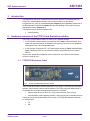
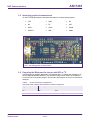
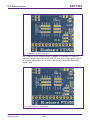
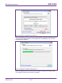
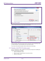
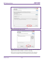
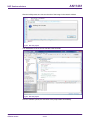
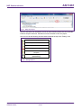
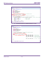
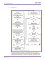
AN11461 Quick Start Up Guide PTEV501B Board Rev. 1.2 — 6 March 2014 277612 Application note COMPANY PUBLIC Document information Info Content Keywords PTEV501, PT501, LPCXpresso, MCU, Code Red, eclipse, LPC1227, reader library Abstract This application note is related to the installation procedures of the PTEV501B Board. It describes the board and the required actions to hand on quickly the Evaluation board. AN11461 NXP Semiconductors PTEV501B Quick Startup Guide Revision history Rev Date Description 1.2 20140306 Updated clock configuration for use with external clock source 1.1 20131212 Added Mass erase description and schematics of PTEV501B analog part 1.0 20131118 First release Contact information For more information, please visit: http://www.nxp.com For sales office addresses, please send an email to: [email protected] AN11461 Application note COMPANY PUBLIC All information provided in this document is subject to legal disclaimers. Rev. 1.2 — 6 March 2014 277612 © NXP N.V. 2014. All rights reserved. 2 of 32 AN11461 NXP Semiconductors PTEV501B Quick Startup Guide 1. Introduction This application note gives a detailed overview of the hardware for operating with the PT501 NFC Card Emulation and NFC Peer-to-Peer Solution [1]. We use the LPCXpresso LPC 1227 [4] and the Blueboard (Chapter 2), the installation procedures of the Development Environment (Chapter 5.1) and the handling of the project using the NXP Reader Library (Chapter 5.3). The projects used in this documentation are: • Card Emulation 2. Hardware overview of the PT501 Card Emulation solution The PT501 Card Emulation solution is made up of 2 separate boards: • A PTEV501B Evaluation board [3] provided by NXP (12NC: 9353 029 06699). This board has connectors which are designed to fit exactly to the ones of the companion LPCXpresso LPC 1227 development board. • A commercial LPCXpresso LPC 1227 development board [4] (12NC: 935294603598, Type: OM13008) which can be provided by NXP or bought directly on the market. See [2]. Once the two boards are put together via the connectors, the PT501 Card Emulation solution is ready for use. 2.1 PTEV501B Evaluation board Fig 1. Picture of PTEV501B Evaluation board The PTEV501B Evaluation board embeds the PT501 generic 13.56 MHz communication interface, with matching network and the antenna. The PT501 supports different kind of contactless communication methods and protocols at 13.56 MHz: • Passive target device for NFC IP-1 mode communication (Peer to Peer) • Card operation mode supporting ISO/IEC 14443-A and FeliCa compliant protocol Thanks to the relevant solder bridges, the host link of PTEV501B Evaluation board can be configured for: AN11461 Application note COMPANY PUBLIC • I²C • SPI All information provided in this document is subject to legal disclaimers. Rev. 1.2 — 6 March 2014 277612 © NXP N.V. 2014. All rights reserved. 3 of 32 AN11461 NXP Semiconductors PTEV501B Quick Startup Guide Fig 2. Picture of solder bridges in default configuration The default interface configuration of the PTEV501B Evaluation board is SPI. The detailed interface configuration is described in section 2.6. 2.1.1 Comparison with the PNEV512B Evaluation board The PTEV501B has basically the same board layout as the PNEV512B Evaluation board. Since the PT501 acts as passive device in card emulation and P2P mode, all parts for the transmitter output are not necessary. This is visible if one compares the two boards as in Figure 3. Fig 3. Comparison of PTEV501B and PNEV512B AN11461 Application note COMPANY PUBLIC All information provided in this document is subject to legal disclaimers. Rev. 1.2 — 6 March 2014 277612 © NXP N.V. 2014. All rights reserved. 4 of 32 AN11461 NXP Semiconductors PTEV501B Quick Startup Guide The list of necessary components for the receiver part find here: Table 1. Necessary components of the PTEV501B analog part Component type Part Nr. Value Capacitor C12, C15, C20 1 nF Capacitor C13, C25 220 pF Resistor R16 1 kΩ Resistor R19 0Ω Resistor R25, R26, R27, R29 4,4 Ω Fig 4. Schematics of the PTEV501B analog part Fig 5. Schematics of the PNEV512B analog part AN11461 Application note COMPANY PUBLIC All information provided in this document is subject to legal disclaimers. Rev. 1.2 — 6 March 2014 277612 © NXP N.V. 2014. All rights reserved. 5 of 32 AN11461 NXP Semiconductors PTEV501B Quick Startup Guide Figure 4 and 5 show the analog parts of the PTEV501B and PNEV512B boards. DNP (do not place) means that this components have routed footprints but are not placed on the PCB to show the differences to the PNEV512B. Table 2. Unused components of the PNEV512B analog part Component type Part Nr. Inductor L2, L3, L4 Resistor R23 Capacitor C7, C8, C14, C16, C17, C18, C21, C22, C23, C24 2.2 CE certification of the Blueboard The PTEV501B V1.0 is CE certified. 2.3 LPCXpresso LPC1227 development board The LPC1227 development board integrates a NXP ARM Cortex-M0 microcontroller LPC1227 with 128 Kbytes of Flash memory and 8 Kbytes of RAM. It integrates a lot of hardware parts: • 1 Serial UART interface, • 1 SPI controller, • 1 I²C controller, • Serial Wire test/debug interface, • For detailed information, see LPC12xx User Manual [5] The LPCXpresso board contains a JTAG/ SWD debugger called the “LPC-Link” and a target MCU. LPC-Link is equipped with a 10-pin JTAG header and it seamlessly connects to the target via USB (the USB interface and other debug features are provided by NXP’s ARM9 based LPC3154 MCU). Fig 6. Picture of LPCXpresso LPC1227 development board 2.4 Preparation of the hardware The first step after unpacking the Blue Board and the LPCXpresso is soldering the connectors onto the boards to get them together. In our example we use a multipoint connector as one can see on the pictures below. AN11461 Application note COMPANY PUBLIC All information provided in this document is subject to legal disclaimers. Rev. 1.2 — 6 March 2014 277612 © NXP N.V. 2014. All rights reserved. 6 of 32 AN11461 NXP Semiconductors PTEV501B Quick Startup Guide Fig 7. Multipoint Connectors we used One may buy these connectors at any electronic store. Here are some examples [7]. After soldering the connectors connect the boards as shown on the following figure. Fig 8. LPCXpresso with the Multipoint Connectors Now the hardware is ready to use. Please connect the LPCXpresso board with the Blueboard. Fig 9. AN11461 Application note COMPANY PUBLIC Connect the two boards All information provided in this document is subject to legal disclaimers. Rev. 1.2 — 6 March 2014 277612 © NXP N.V. 2014. All rights reserved. 7 of 32 AN11461 NXP Semiconductors PTEV501B Quick Startup Guide 2.5 Interesting points of measurement On the PTEV501B Evaluation board are test pads for measurement purposes. • VCC • GND • D5 • D6 • D7 • ALE • AUX1 • AUX2 • SIGIN • SIGOUT • IRQ • VMID Fig 10. Interesting points of measurement 2.6 Preparing the Blueboard for the use with SPI or I2C The Blueboard is generally delivered in SPI configuration. To change the interface to I²C the four appropriate 0R0 resistors in the interface config section need to be resoldered on the I²C side of the solder jumpers. Also the two 0R0 resistors at A0 and A1 need to be changed. Table 3. A0 and A1 interface configuration Appropriate solder jumpers (0R0 resistors) for interface configuration Signal Interface type AN11461 Application note COMPANY PUBLIC SPI I²C A0 R20 R21 A1 R24 R23 All information provided in this document is subject to legal disclaimers. Rev. 1.2 — 6 March 2014 277612 © NXP N.V. 2014. All rights reserved. 8 of 32 AN11461 NXP Semiconductors PTEV501B Quick Startup Guide Fig 11. Blueboard in SPI configuration The I²C-address can be configured either by software or by hardware. To set the I²Caddress by hardware the solder jumpers in the I²C config section (see Figure 11) has to be connected appropriately. R3, R7 and R13 are logically LOW and R4, R8 and R15 logically HIGH. Fig 12. Blueboard in I²C configuration AN11461 Application note COMPANY PUBLIC All information provided in this document is subject to legal disclaimers. Rev. 1.2 — 6 March 2014 277612 © NXP N.V. 2014. All rights reserved. 9 of 32 AN11461 NXP Semiconductors PTEV501B Quick Startup Guide 3. PT501 clock requirements The PT501 is characterized to a frequency of 27.12 MHz, but it is possible to operate it with a frequency between 1 MHz and 33 MHz on pin OSZIN. As clock source any stable CLK-signal in this frequency range can be used. To avoid that unwanted noise disturbs the clock, the PT501 has an internal frequency check. The operating frequency of 13.56 MHz and the expected 13.56 MHz, derived from the 27.12MHz clock source are compared. If the frequencies differ too much, the received RF-clock is assumed to be a disturbance and the card cannot be used. This is the case e.g. if an external clock of 2 MHz is provided on the CLK input pin. To use other frequencies than 13.56 MHz the RF-clock frequency check can be disabled by register settings. See 3.2 Software configuration. Note: The correct register settings to disable the frequency check are mandatory if a clock below 23 MHz is used, between 23 MHz and 33 MHz it can be enabled. 3.1 Hardware configuration The PTEV501B is prepared to be used in conjunction with an on board crystal oscillator or a clock generated by the LPC1227 LPCXpresso Board. The following table describes the necessary soldering changes for the different configurations: Table 4. PT501 clock configuration R31 can be placed as 0Ω resistor or solder bridge Clock source R31 XT1 C29 C30 Crystal oscillator (default) Not placed 27,12 MHz 15pF 15pF External clock from LPC1227 LPCXpresso Board 0Ω Not placed Not placed Not placed Fig 13. Crystal oscillator as clock source (default) AN11461 Application note COMPANY PUBLIC All information provided in this document is subject to legal disclaimers. Rev. 1.2 — 6 March 2014 277612 © NXP N.V. 2014. All rights reserved. 10 of 32 AN11461 NXP Semiconductors PTEV501B Quick Startup Guide Fig 14. LPC1227 as clock source Figure 15a shows a snippet of the PTEV501B schematics. If one would like to use a different CLK-source as described above, the external clock signal should be connected to pin OSCIN by connecting to one of the component pads shown in Figure 15b. a. b. Fig 15. Schematics of the PTEV501B clock input 3.2 Software configuration This section describes the software configuration for the PTEV501B with an external clock source. This can either be the CLKOUT-function of the LPC1227 or any stable clock signal in the frequency range of 1 MHz to 33 MHz. 3.2.1 LPC1227 LPCXpresso Board as clock source Please make sure to change the hardware configuration as defined in section 3 before loading and running the modified software package into the LPC1227 to avoid breaking any hardware. AN11461 Application note COMPANY PUBLIC All information provided in this document is subject to legal disclaimers. Rev. 1.2 — 6 March 2014 277612 © NXP N.V. 2014. All rights reserved. 11 of 32 AN11461 NXP Semiconductors PTEV501B Quick Startup Guide To use the PTEV501B with the LPC1227 LPCXpresso Board as external clock source some modifications need to be done in the system_LPC12xx.c file: 3.2.1.1 Configure the Main Clock For this example configuration a frequency of 24 MHz is used. To achieve this following settings of the SYSPLLCTRL register are required. The SYSPLLCLKSEL_Val (0x01 for System Oscillator) defines the clock source for the internal System PLL which must be activated by setting the SYSPLL_SETUP to 1. The SYSPLLCTRL_Val specifies the output frequency of the System PLL. This can be configured by the Bits 0-6 of the SYSPLLCTRL register, in this case a frequency of 24 MHz. Other system clock settings may also be used as long as the LPC1227 generated clock is in the range as defined in section 3. Please refer to the LPC122x User Manual [6] and Data Sheet [5] for detailed description of the supported configurations. The MAINCLKSEL_Val sets the clock source for the system Main clock (0x3 for the System PLL output). Fig 16. Main Clock configuration 3.2.1.2 Enable the CLKOUT functionality To use the CLKOUT pin of the LPC1227 the CLKOUTCLK_SETUP has to be enabled. The CLKOUTCLKSEL_Val specifies the clock source, here 0x3 for the Main clock at 24 MHz, so no further division by the CLKOUTCLKDIV_Val is needed (0x01). Fig 17. CLKOUT configuration AN11461 Application note COMPANY PUBLIC All information provided in this document is subject to legal disclaimers. Rev. 1.2 — 6 March 2014 277612 © NXP N.V. 2014. All rights reserved. 12 of 32 AN11461 NXP Semiconductors PTEV501B Quick Startup Guide 3.2.1.3 Configure the CLKOUT setup With the enabled CLKOUTCLK_SETUP in the previous section the #if statement for the CLKOUT configuration is true. The CLKOUT function is routed to PIO0_12 and needs to be configured (0x02). It is very important to update the clock source by toggling the CLKOUTUEN register. Fig 18. CLKOUT setup configuration For detailed information about the LPC1227 clock configuration and register settings please refer to the product datasheet and user manual. 3.2.2 Other clock source If any other clock source with a frequency between 1 MHz and 23 MHz is used for the PT501, following register settings are mandatory to turn off the frequency check: 1. Write 0xBF to register 0x3C 2. Read from register 0x3C In the Card Emulation software package this register setting can be activated/deactivated by the #define PT501_EXT_XTAL statement in main.c. Fig 19. Register settings for the frequency check function in main.c AN11461 Application note COMPANY PUBLIC All information provided in this document is subject to legal disclaimers. Rev. 1.2 — 6 March 2014 277612 © NXP N.V. 2014. All rights reserved. 13 of 32 AN11461 NXP Semiconductors PTEV501B Quick Startup Guide 4. Installation of the LPCXpresso Board The guidelines to install the reader are as follows: • Connect the LPCXpresso Board to a real USB2.0 port of the PC (for speed reasons) using the mini-USB connector. The PC detects and installs the Board automatically. • Once the Board is installed, open the Device Manager of the PC to check that the installation is successful. The item “USB Device with DFU Capabilities” is displayed. Please be sure to always connect both USB ports to the computer. If the USB port of the Blueboard is not connected to an USB port, it won’t work because of the missing power. Fig 20. Enumeration of the LPCXpresso Board in Device Manager Window 5. Managing the PT501 CE solution project with LPCXpresso IDE The PT501 Card emulation solution project is delivered in a zip package. It can be extracted, edited, compiled and linked with LPCXpresso™ IDE. LPCXpresso™ is a new, low-cost development platform available from NXP. It supports NXP's ARM-based LPC microcontrollers. The platform is comprised of a simplified Eclipse-based IDE and low-cost target boards which include an attached JTAG debugger. Use at least the LPCXpresso version 4.2 or higher to benefit a bug-free IDE and the upto-date features. AN11461 Application note COMPANY PUBLIC All information provided in this document is subject to legal disclaimers. Rev. 1.2 — 6 March 2014 277612 © NXP N.V. 2014. All rights reserved. 14 of 32 AN11461 NXP Semiconductors PTEV501B Quick Startup Guide This tool can be freely downloaded from the LPCXpresso website [2]. Before one can download the software, it is necessary to create an account. Creating an account is absolutely free. 5.1 Installation of LPCXpresso IDE The IDE is installed into a single directory, of one’s choice. Multiple versions cans be installed simultaneously without any issues. The installation starts after double-clicking the installer file. Then click “next” on the setup wizard. Fig 21. LPCXpresso installation setup wizard 1 Then read the license agreement then click next. AN11461 Application note COMPANY PUBLIC All information provided in this document is subject to legal disclaimers. Rev. 1.2 — 6 March 2014 277612 © NXP N.V. 2014. All rights reserved. 15 of 32 AN11461 NXP Semiconductors PTEV501B Quick Startup Guide Fig 22. LPCXpresso installation setup wizard 2 There are numbers of other screens on the setup wizard but generally the default options can be accepted. After installation, an information file will be displayed. Click “Next” to accomplish the installation. Fig 23. LPCXpresso installation setup wizard 3 After this installation step one will be asked if he wants to install some required drivers. The installation of these drivers should be accepted. AN11461 Application note COMPANY PUBLIC All information provided in this document is subject to legal disclaimers. Rev. 1.2 — 6 March 2014 277612 © NXP N.V. 2014. All rights reserved. 16 of 32 AN11461 NXP Semiconductors PTEV501B Quick Startup Guide Fig 24. Windows Security dialog After the setup wizard has finished one can launch the newly installed IDE. Fig 25. LPCXpresso installation setup wizard 4 AN11461 Application note COMPANY PUBLIC All information provided in this document is subject to legal disclaimers. Rev. 1.2 — 6 March 2014 277612 © NXP N.V. 2014. All rights reserved. 17 of 32 AN11461 NXP Semiconductors PTEV501B Quick Startup Guide Fig 26. LPCXpresso IDE Directly after the first start of the Eclipse IDE one will see an info dialog, that this is only an unregistered copy of LPCXpresso IDE. Just confirm the dialog and follow the instructions on the Welcome Screen to get a registered version without the debug limit of 8k. The registration is free and needs one to navigate to the website of Code Red. The Link is shown in the menu, Help Product activation Create Serial number and Activate... Fig 27. Product activation AN11461 Application note COMPANY PUBLIC All information provided in this document is subject to legal disclaimers. Rev. 1.2 — 6 March 2014 277612 © NXP N.V. 2014. All rights reserved. 18 of 32 AN11461 NXP Semiconductors PTEV501B Quick Startup Guide Fig 28. Product activation If one doesn’t already have an account at Code Red, please sign up to get an activation code. The code will be sent to the provided e-mail address. Fig 29. Product activation Once the activation code arrives please open the activation window by pointing to Help Product activation Enter Activation code, and enter the code. The success of the product activation will be confirmed by an info dialog. 5.2 Extraction of the PT501 CE solution project Once the LPCXpresso™ IDE is installed on a Computer, the sequence of installing the reference reader project is indicated: AN11461 Application note COMPANY PUBLIC • Start the LPCXpresso™ IDE. • Select the option “Import project(s)” (see picture below). • Browse the zip archive. All information provided in this document is subject to legal disclaimers. Rev. 1.2 — 6 March 2014 277612 © NXP N.V. 2014. All rights reserved. 19 of 32 AN11461 NXP Semiconductors PTEV501B Quick Startup Guide • LPCXpresso™ IDE unzips the software package. • The software package is ready for use. Fig 30. Importing a project into the LPCXpresso IDE At the Quick Panel on the left side, choose “Import projects(s)”. AN11461 Application note COMPANY PUBLIC All information provided in this document is subject to legal disclaimers. Rev. 1.2 — 6 March 2014 277612 © NXP N.V. 2014. All rights reserved. 20 of 32 AN11461 NXP Semiconductors PTEV501B Quick Startup Guide Fig 31. Importing a project into the LPCXpresso IDE Browse the desired project and click “Next”. Fig 32. Importing a project into the LPCXpresso IDE When the import process has finished one can start browsing the code. Most interesting might be the main.c which is located in ../src/main.c in the project. Before one can run the project, the Evaluation board with the PT501 needs to be connected to the computer. Wait until the according drivers have been installed. AN11461 Application note COMPANY PUBLIC All information provided in this document is subject to legal disclaimers. Rev. 1.2 — 6 March 2014 277612 © NXP N.V. 2014. All rights reserved. 21 of 32 AN11461 NXP Semiconductors PTEV501B Quick Startup Guide 5.3 Start the project One can quickly start the reader project by editing the main function in the module main.c. This function first performs the hardware initializations of the LPC1227 and the PT501. Detailed descriptions of the code in the form of comments are provided in the main.c file. This should provide a detailed overview of how to initialize certain components. 5.3.1 Run the project Before running the project, please ensure that the LPCXpresso with the PTEV501B Evaluation board is connected with the computer. Fig 33. Run the project Choose the desired project and click at the left side the Debug Button like shown at the example picture. Fig 34. Run the project AN11461 Application note COMPANY PUBLIC All information provided in this document is subject to legal disclaimers. Rev. 1.2 — 6 March 2014 277612 © NXP N.V. 2014. All rights reserved. 22 of 32 AN11461 NXP Semiconductors PTEV501B Quick Startup Guide After the build process one can see the size of the image in the console window. Fig 35. Run the project The initialization of the LPC-Link can take a few seconds. Fig 36. Run the project After the software upload, the execution of the project starts immediately. AN11461 Application note COMPANY PUBLIC All information provided in this document is subject to legal disclaimers. Rev. 1.2 — 6 March 2014 277612 © NXP N.V. 2014. All rights reserved. 23 of 32 AN11461 NXP Semiconductors PTEV501B Quick Startup Guide Fig 37. Stop the project After the execution has reached the end of the main function please click the Terminate button to stop the execution. Otherwise one won’t be able to rerun the project. One can now do the following with the buttons towards the top of the “Debug” view: Run the program. Step over C/C++ line. Step into a function. Stop the debugger. Pause execution of the running program. Instruction stepping mode (disassembly). Fig 38. Debug Buttons AN11461 Application note COMPANY PUBLIC All information provided in this document is subject to legal disclaimers. Rev. 1.2 — 6 March 2014 277612 © NXP N.V. 2014. All rights reserved. 24 of 32 AN11461 NXP Semiconductors PTEV501B Quick Startup Guide 6. Card Emulation - Associated Project 6.1 Tag Type 2 and Type 4 Card Emulation This example only works with the LPCXpresso LPC1227 development board. The PT501 supports 2 different operating modes: • Passive target device for NFC IP-1 mode communication (Peer to Peer) • Card operation mode supporting ISO/IEC 14443-A and FeliCa compliant protocol The card operation mode is passive mode, in which the PT501 does not generate an RF field but acts as a card that modulates the field for communication with the reader. The IC only supports parts of the ISO/IEC 14443-A protocol, the ISO/IEC 14443-4 as well as the ISO/IEC 7816-4 commands need to be provided by the Microcontroller. A specification to store data for any kind of service and application is specified in the NFC Forum and it is called NFC Data Exchange Format. Storing NDEF formatted data inside contactless card products as mapping models as well as the management of NFC forum device as a specific platform such as a NFC Forum Type 4 Tag are defined in [9]. The following project shows an exemplary implementation of a Tag 4 Type Card on the PN501. Therefore one NDEF File and one capability container (CC) file, with ISO file identifier (ISO FID) equal to E103h, are presented to the reader. 6.1.1 Configuration of the example project In order to change some of the possible options before compiling the project, the file "src\nxprdlib\intfs\phCardEmu_Options.h" should be edited. This file contains toggles to enable/disable the T2T and T4T functionality, memory sizes, as well as the pin numbers in which the PT501 chip is connected to the LPC1227. Further options are also indicated on the file. Before flashing the modified project it is mandatory to perform a Mass erase on the flash memory of the LPC1227. This can be achieved by clicking the Program Flash icon in the LPCXpresso IDE. Fig 39. Program Flash icon in LPCXpresso IDE In the Program Flash wizard the Mass erase feature can be found in the Erase flash memory tab. After activating the Mass erase algorithm click OK to perform the procedure. AN11461 Application note COMPANY PUBLIC All information provided in this document is subject to legal disclaimers. Rev. 1.2 — 6 March 2014 277612 © NXP N.V. 2014. All rights reserved. 25 of 32 AN11461 NXP Semiconductors PTEV501B Quick Startup Guide Fig 40. Program Flash wizard with Erase flash memory tab 6.1.2 Changing the NDEF message The predefined NDEF message can be changed in the following files: • AN11461 Application note COMPANY PUBLIC T4T: ../src/nxprdlib/comps/phce7816p4T_Apps/phce7816p4T_T4T_Const.c All information provided in this document is subject to legal disclaimers. Rev. 1.2 — 6 March 2014 277612 © NXP N.V. 2014. All rights reserved. 26 of 32 AN11461 NXP Semiconductors PTEV501B Quick Startup Guide Fig 41. Change NDEF content for T4T • T2T: ../src/nxprdlib/comps/phceT2TCmdHdl/src/Sw/phceT2T_Const.c Fig 42. Change NDEF content for T2T AN11461 Application note COMPANY PUBLIC All information provided in this document is subject to legal disclaimers. Rev. 1.2 — 6 March 2014 277612 © NXP N.V. 2014. All rights reserved. 27 of 32 AN11461 NXP Semiconductors PTEV501B Quick Startup Guide 6.1.3 Program flow Fig 43. Program flow of the Card Emulation application The first blocks describe the initialization of the necessary layers and components independent of the card emulation. Depending which tag type is used the appropriate component will then be initialized. If Tag Type 2 and Tag Type 4 are enabled, both are AN11461 Application note COMPANY PUBLIC All information provided in this document is subject to legal disclaimers. Rev. 1.2 — 6 March 2014 277612 © NXP N.V. 2014. All rights reserved. 28 of 32 AN11461 NXP Semiconductors PTEV501B Quick Startup Guide being initialized. After applying the protocol settings, the PT501 waits for a successful activation or the card side. According to the first command (RATS – yes or no) after the card activation the appropriate tag type component starts. 7. References [1] PT501 data sheet http://www.nxp.com/documents/data_sheet/PT501.pdf [2] LPCXpresso website www.nxp.com/redirect/lpcware.com/lpcxpresso/downloads/older [3] PTEV501 Evaluation board http://www.nxp.com/demoboard/PTEV501.html [4] LPC1227 LPCXpresso Board www.nxp.com/redirect/embeddedartists.com/products/lpcxpresso/lpc1227_xpr.php [5] LPC122x family data sheet http://www.nxp.com/documents/data_sheet/LPC122X.pdf AN11461 Application note COMPANY PUBLIC [6] LPC122X family User Manual http://www.nxp.com/documents/user_manual/UM10441.pdf [7] Multipoint Connectors we used: Grid Dimension: 2.54mm, at least 27 pins www.nxp.com/redirect/conrad.at/ce/de/product/741119/STIFTLEISTE-1-X-36POLIG-VERGOL-RM-254 and www.nxp.com/redirect/conrad.at/ce/de/product/736427/BUCHSENLEISTEEINREIHIG-36-POLIG-RM254 [8] Direct link to the NXP Reader Library http://www.nxp.com/documents/software/200310.zip [9] TYPE 4 TAG: NFC Forum, Type 4 Tag Operation Specification, Version 1.0, March 13, 2007 www.nxp.com/redirect/nfc-forum.org/specs All information provided in this document is subject to legal disclaimers. Rev. 1.2 — 6 March 2014 277612 © NXP N.V. 2014. All rights reserved. 29 of 32 AN11461 NXP Semiconductors PTEV501B Quick Startup Guide 8. Legal information 8.1 Definitions Draft — The document is a draft version only. The content is still under internal review and subject to formal approval, which may result in modifications or additions. NXP Semiconductors does not give any representations or warranties as to the accuracy or completeness of information included herein and shall have no liability for the consequences of use of such information. 8.2 Disclaimers Limited warranty and liability — Information in this document is believed to be accurate and reliable. However, NXP Semiconductors does not give any representations or warranties, expressed or implied, as to the accuracy or completeness of such information and shall have no liability for the consequences of use of such information. In no event shall NXP Semiconductors be liable for any indirect, incidental, punitive, special or consequential damages (including - without limitation lost profits, lost savings, business interruption, costs related to the removal or replacement of any products or rework charges) whether or not such damages are based on tort (including negligence), warranty, breach of contract or any other legal theory. Notwithstanding any damages that customer might incur for any reason whatsoever, NXP Semiconductors’ aggregate and cumulative liability towards customer for the products described herein shall be limited in accordance with the Terms and conditions of commercial sale of NXP Semiconductors. Right to make changes — NXP Semiconductors reserves the right to make changes to information published in this document, including without limitation specifications and product descriptions, at any time and without notice. This document supersedes and replaces all information supplied prior to the publication hereof. Suitability for use — NXP Semiconductors products are not designed, authorized or warranted to be suitable for use in life support, life-critical or safety-critical systems or equipment, nor in applications where failure or malfunction of an NXP Semiconductors product can reasonably be expected to result in personal injury, death or severe property or environmental damage. NXP Semiconductors accepts no liability for inclusion and/or use of NXP Semiconductors products in such equipment or applications and therefore such inclusion and/or use is at the customer’s own risk. Applications — Applications that are described herein for any of these products are for illustrative purposes only. NXP Semiconductors makes no representation or warranty that such applications will be suitable for the specified use without further testing or modification. Customers are responsible for the design and operation of their applications and products using NXP Semiconductors products, and NXP Semiconductors accepts no liability for any assistance with applications or customer product design. It is customer’s sole responsibility to determine whether the NXP Semiconductors product is suitable and fit for the customer’s applications and products planned, as well as for the planned application and use of customer’s third party customer(s). Customers should provide appropriate design and operating safeguards to minimize the risks associated with their applications and products. NXP Semiconductors does not accept any liability related to any default, damage, costs or problem which is based on any weakness or default in the customer’s applications or products, or the application or use by customer’s third party customer(s). Customer is responsible for doing all necessary AN11461 Application note COMPANY PUBLIC testing for the customer’s applications and products using NXP Semiconductors products in order to avoid a default of the applications and the products or of the application or use by customer’s third party customer(s). NXP does not accept any liability in this respect. Export control — This document as well as the item(s) described herein may be subject to export control regulations. Export might require a prior authorization from competent authorities. Evaluation products — This product is provided on an “as is” and “with all faults” basis for evaluation purposes only. NXP Semiconductors, its affiliates and their suppliers expressly disclaim all warranties, whether express, implied or statutory, including but not limited to the implied warranties of noninfringement, merchantability and fitness for a particular purpose. The entire risk as to the quality, or arising out of the use or performance, of this product remains with customer. In no event shall NXP Semiconductors, its affiliates or their suppliers be liable to customer for any special, indirect, consequential, punitive or incidental damages (including without limitation damages for loss of business, business interruption, loss of use, loss of data or information, and the like) arising out the use of or inability to use the product, whether or not based on tort (including negligence), strict liability, breach of contract, breach of warranty or any other theory, even if advised of the possibility of such damages. Notwithstanding any damages that customer might incur for any reason whatsoever (including without limitation, all damages referenced above and all direct or general damages), the entire liability of NXP Semiconductors, its affiliates and their suppliers and customer’s exclusive remedy for all of the foregoing shall be limited to actual damages incurred by customer based on reasonable reliance up to the greater of the amount actually paid by customer for the product or five dollars (US$5.00). The foregoing limitations, exclusions and disclaimers shall apply to the maximum extent permitted by applicable law, even if any remedy fails of its essential purpose. 8.3 Licenses Purchase of NXP ICs with ISO/IEC 14443 type B functionality This NXP Semiconductors IC is ISO/IEC 14443 Type B software enabled and is licensed under Innovatron’s Contactless Card patents license for ISO/IEC 14443 B. The license includes the right to use the IC in systems and/or end-user equipment. RATP/Innovatron Technology 8.4 Trademarks Notice: All referenced brands, product names, service names and trademarks are property of their respective owners. MIFARE — is a trademark of NXP N.V. DESFire — is a trademark of NXP N.V. MIFARE Ultralight — is a trademark of NXP N.V. MIFARE Plus — is a trademark of NXP N.V. All information provided in this document is subject to legal disclaimers. Rev. 1.2 — 6 March 2014 277612 © NXP N.V. 2014. All rights reserved. 30 of 32 AN11461 NXP Semiconductors PTEV501B Quick Startup Guide 9. List of figures Fig 1. Fig 2. Fig 3. Fig 4. Fig 5. Fig 6. Fig 7. Fig 8. Fig 9. Fig 10. Fig 11. Fig 12. Fig 13. Fig 14. Fig 15. Fig 16. Fig 17. Fig 18. Fig 19. Fig 20. Fig 21. Picture of PTEV501B Evaluation board ............ 3 Picture of solder bridges in default configuration ..................................................... 4 Comparison of PTEV501B and PNEV512B ...... 4 Schematics of the PTEV501B analog part ........ 5 Schematics of the PNEV512B analog part........ 5 Picture of LPCXpresso LPC1227 development board ................................................................. 6 Multipoint Connectors we used ......................... 7 LPCXpresso with the Multipoint Connectors ..... 7 Connect the two boards .................................... 7 Interesting points of measurement .................... 8 Blueboard in SPI configuration.......................... 9 Blueboard in I²C configuration........................... 9 Crystal oscillator as clock source (default) ...... 10 LPC1227 as clock source ............................... 11 Schematics of the PTEV501B clock input ....... 11 Main Clock configuration ................................. 12 CLKOUT configuration .................................... 12 CLKOUT setup configuration .......................... 13 Register settings for the frequency check function in main.c ............................................ 13 Enumeration of the LPCXpresso Board in Device Manager Window ................................ 14 LPCXpresso installation setup wizard 1 .......... 15 AN11461 Application note COMPANY PUBLIC Fig 22. Fig 23. Fig 24. Fig 25. Fig 26. Fig 27. Fig 28. Fig 29. Fig 30. Fig 31. Fig 32. Fig 33. Fig 34. Fig 35. Fig 36. Fig 37. Fig 38. Fig 39. Fig 40. Fig 41. Fig 42. Fig 43. LPCXpresso installation setup wizard 2 ..........16 LPCXpresso installation setup wizard 3 ..........16 Windows Security dialog .................................17 LPCXpresso installation setup wizard 4 ..........17 LPCXpresso IDE .............................................18 Product activation ............................................18 Product activation ............................................19 Product activation ............................................19 Importing a project into the LPCXpresso IDE ..20 Importing a project into the LPCXpresso IDE ..21 Importing a project into the LPCXpresso IDE ..21 Run the project ................................................22 Run the project ................................................22 Run the project ................................................23 Run the project ................................................23 Stop the project ...............................................24 Debug Buttons ................................................24 Program Flash icon in LPCXpresso IDE .........25 Program Flash wizard with Erase flash memory tab ...................................................................26 Change NDEF content for T4T........................27 Change NDEF content for T2T........................27 Program flow of the Card Emulation application .......................................................28 All information provided in this document is subject to legal disclaimers. Rev. 1.2 — 6 March 2014 277612 © NXP N.V. 2014. All rights reserved. 31 of 32 AN11461 NXP Semiconductors PTEV501B Quick Startup Guide 10. Contents 1. 2. Introduction ......................................................... 3 Hardware overview of the PT501 Card Emulation solution .............................................. 3 2.1 PTEV501B Evaluation board.............................. 3 2.1.1 Comparison with the PNEV512B Evaluation board .................................................................. 4 2.2 CE certification of the Blueboard ........................ 6 2.3 LPCXpresso LPC1227 development board ....... 6 2.4 Preparation of the hardware ............................... 6 2.5 Interesting points of measurement ..................... 8 2.6 Preparing the Blueboard for the use with SPI or 2 I C ...................................................................... 8 3. PT501 clock requirements ................................ 10 3.1 Hardware configuration .................................... 10 3.2 Software configuration ..................................... 11 3.2.1 LPC1227 LPCXpresso Board as clock source . 11 3.2.1.1 Configure the Main Clock ................................. 12 3.2.1.2 Enable the CLKOUT functionality..................... 12 3.2.1.3 Configure the CLKOUT setup .......................... 13 3.2.2 Other clock source ........................................... 13 4. Installation of the LPCXpresso Board ............. 14 5. Managing the PT501 CE solution project with LPCXpresso IDE ................................................ 14 5.1 Installation of LPCXpresso IDE ........................ 15 5.2 Extraction of the PT501 CE solution project ..... 19 5.3 Start the project ................................................ 22 5.3.1 Run the project ................................................. 22 6. Card Emulation - Associated Project .............. 25 6.1 Tag Type 2 and Type 4 Card Emulation .......... 25 6.1.1 Configuration of the example project................ 25 6.1.2 Changing the NDEF message.......................... 26 6.1.3 Program flow .................................................... 28 7. References ......................................................... 29 8. Legal information .............................................. 30 8.1 Definitions ........................................................ 30 8.2 Disclaimers....................................................... 30 8.3 Licenses ........................................................... 30 8.4 Trademarks ...................................................... 30 9. List of figures..................................................... 31 10. Contents ............................................................. 32 Please be aware that important notices concerning this document and the product(s) described herein, have been included in the section 'Legal information'. © NXP N.V. 2014. All rights reserved. For more information, visit: http://www.nxp.com For sales office addresses, please send an email to: [email protected] Date of release: 6 March 2014 277612 Document identifier: AN11461