1
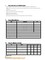
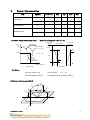
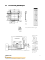
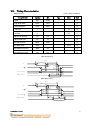
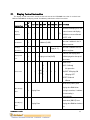
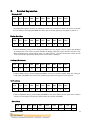
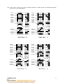
MGL5128 128x64 Graphic LCD Module
User Manual
Version: 1.0.0
January 2005
Table of Contents
I
Precautions in use of LCD Modules
2
II
General Specification
2
III
Absolute Maximum Ratings
2
IV
Electrical Characteristics
3
V
Optical Characteristics
4
VI
Interface Description
5
VII
Contour Drawing & Block Diagram
6
VIII
Timing Characteristics
7
IX
Display Control Instruction
8
X
Detailed Explanation
9
XI
Quality Assurance
12
XII
Reliability
13
XIII
Backlight Information
14
Related Document:
WiRobot SDK API Reference Manual
Copyright © Dr Robot Inc. 2004
1
I.
Precautions in use of LCD Modules
(1)Avoid applying excessive shocks to the module or making any alterations or modifications to it.
(2)Don’t make extra holes on the printed circuit board, modify its shape or change the components of LCD
module.
(3)Don’t disassemble the LCM.
(4)Don’t operate it above the absolute maximum rating.
(5)Don’t drop, bend or twist LCM.
(6)Soldering: only to the I/O terminals.
(7)Storage: please storage in anti-static electricity container and clean environment.
II.
General Specification
Item
Dimension
Unit
128 x 64 Dots
-
75.0 x 52.7 x 8.9(MAX)
mm
View area
60.0 x 32.6
mm
Active area
55.0 x 27.48
mm
Dot size
0.41 x 0.41
mm
Dot pitch
0.44 x 0.44
mm
Number of Characters
Module dimension
LCD type
STN Negative, Transmissive , blue
Duty
1/64
View direction
6 o’clock
Backlight Type
Edge LED White
III.
Absolute Maximum Ratings
Item
Symbol
Min
Typ
Max
Unit
Operating Temperature
TOP
-20
-
+70
•
Storage Temperature
TST
-30
-
+80
•
Input Voltage
VI
0
-
VDD
V
Supply Voltage For Logic
VDD
0
-
6.7
V
Supply Voltage For LCD
VDD-VLCD
0
-
16.7
V
Copyright © Dr Robot Inc. 2004
2
IV.
Electrical Characteristics
Item
Supply Voltage For Logic
Supply Voltage For LCD
Symbol
Condition
Min
Typ
Max
Unit
VDD-VSS
-
4.75
5.0
5.25
V
Ta=-20•
-
-
9.5
V
Ta=25•
-
8.5
-
V
Ta=+70•
7.5
-
-
V
VDD-V0
Input High Volt.
VIH
-
0.7VDD
-
VDD
V
Input Low Volt.
VIL
-
0
-
0.3VDD
V
Output High Volt.
VOH
-
2.4
-
-
V
Output Low Volt.
VOL
-
-
-
0.4
V
Supply Current
IDD
-
-
1.5
-
mA
Copyright © Dr Robot Inc. 2004
3
V.
Optical Characteristics
Item
Symbol
Condition
Min
Typ
Max
Unit
(V)
CR•2
10
-
105
deg
(H)
CR•2
-30
-
30
deg
CR
-
-
3
-
-
T rise
-
-
200
300
ms
T fall
-
-
200
300
ms
View Angle
Contrast Ratio
Response Time
Definition of Operation Voltage (Vop)
Definition of Response Time ( Tr , Tf )
Non-selected
Conition
Selected Wave
Intensity
100%
Non-selected Wave
Selected Conition
Non-selected
Conition
Intensity
10%
Cr Max
Cr = Lon / Loff
Vop
90%
100%
Tr
Driving Voltage(V)
[positive type]
Tf
[positive type]
Conditions :
Operating Voltage : Vop
Viewing Angle( , ) : 0°, 0°
Frame Frequency : 64 HZ
Driving Waveform : 1/N duty , 1/a bias
Definition of viewing angle(CR•2)
θf
φl
θb
θ
φr
φ
φ
θ
Copyright © Dr Robot Inc. 2004
4
VI.
Interface Description
Pin No.
Symbol
Level
1
VDD
5.0V
2
VSS
0V
3
Vo
4
DB0
H/L
Data bit 0
5
DB1
H/L
Data bit 1
6
DB2
H/L
Data bit 2
7
DB3
H/L
Data bit 3
8
DB4
H/L
Data bit 4
9
DB5
H/L
Data bit 5
10
DB6
H/L
Data bit 6
11
DB7
H/L
Data bit 7
12
CS1
L
Select Column 1~ Column 64
13
CS2
L
Select Column 65~ Column 128
14
RST
L
Reset signal
15
R/W
H/L
H: Read (MPU•Module) , L: Write (MPU•Module)
16
D/I
H/L
H: Data , L : Instruction
17
E
H
Enable signal
18
Vee
-
Negative Voltage output
19
A
-
Power Supply for LED backlight ( + )
20
K
-
Power Supply for LED backlight ( - )
Copyright © Dr Robot Inc. 2004
Description
Supply voltage for logic
Ground
(Variable) Operating voltage for LCD
5
Contour Drawing &Block Diagram
75.0 0.5
70.0
70.6
60.0(VA)
55.0(AA)
7.5
10.0
1.5
52.7 0.5
49.7
44.6
32.6(VA)
27.48(AA)
A
1
2
3
4
5
6
7
8
9
10
11
12
13
14
15
16
17
18
19
20
8.9Max
4.9
2-R1.25 PTH
2-R2.0 PAD
20.12
0.5
2.9
9.05
11.59
2.5
2.2
25.35
VII.
128*64 Dots
10.16
K
1
20
13.37
1.0
2- 2.5 PTH
2- 4.0 PAD
2.5
20- 1.0PTH
20- 1.8PAD
P2.54*19=48.26
37.5
LED B/L
Vdd
Vss
Vo
DB0
DB1
DB2
DB3
DB4
DB5
DB6
DB7
CS1
CS2
RST
R/W
D/I
E
Vee
A
K
0.43
0.39
0.43
0.39
The non-specified tolerance of dimension is 0.3mm.
DOT SIZE
LED B/L Drive Method
Seg Driver
MPU
80 series
or
68 series
E
D/I
R/W
DB0~DB7
KS0108
Seg65~128
Seg Driver
Com Driver
R
Pin19
B/L
R
R
Pin20
Vdd
Vo
Vss
A
B/L
K
LCM
VR
10K~20K
-10V
CS1
CS2
RST
3.Drive from Vdd,Vss
R
A
B/L
K
LCM
(Contrast performance may go down.)
External contrast adjustment.
Copyright © Dr Robot Inc. 2004
A
K
2.Drive from pin19, pin20
Bias and
Power Circuit
KS0108
Seg1~64
FR,M,CL,CLK1,CLK2
128X64 DOT
KS0107
Com1~64
1.Drive from A,K
Recommanded Value
VLED= 4.1V, ILED= 100mA
R= 8Ω(1/2 Watt)
6
VIII.
Timing Characteristics
MPU Interface
(T=25•, VDD=+5.0V±0.5)
Characteristic
Symbol
Min
Typ
Max
Unit
E cycle
tcyc
1000
-
-
ns
E high level width
twhE
450
-
-
ns
E low level width
twlE
450
-
-
ns
E rise time
tr
-
-
25
ns
E tall time
tf
-
-
25
ns
Address set-up time
tas
140
-
-
ns
Address hold time
tah
10
-
-
ns
Data set-up time
tdsw
200
-
-
ns
Data delay time
tddr
-
-
320
ns
Data hold time (write)
tdhw
10
-
-
ns
Data hold time (read)
tdhr
20
-
-
ns
MPU Read Timing
tc y c
E
tw IE
2 .0 V
0 .8 V
tr
tw h E
ta s
R /W
tf
ta h
ta s
C S 1 ,C S 2 ,D /I
ta h
2 .0 V
0 .8 V
td s w
td h w
D B 0 to D B 7
MPU Write Timing
tc y c
tw IE
E
R /W
2 .0 V
tw h E
0 .8 V
tr
2 .0 V
0 .8 V
tf
ta h
ta s
ta s
C S 1 ,C S 2 ,D /I
ta h
2 .0 V
0 .8 V
td d r
td h r
D B 0 to D B 7
Copyright © Dr Robot Inc. 2004
7
IX.
Display Control Instruction
The display control instructions control the internal state of the KS0108B. Instruction is received from
MPU to KS0108B for the display control. The following table shows various instructions
R/
D/I
Instruction
DB7 DB6 DB5 DB4 DB3 DB2 DB1 DB0 Function
W
Controls the display on or off.
Internal status and display
Display
0
0
0
0
1
1
1
1
1
0/1
RAM data are not affected.
ON/OFF
0:OFF, 1:ON
Sets the Y address in the Y
Set Address
0
0
0
1
Y address (0~63)
address counter.
Sets the X address at the X
Set Page
0
0
1
0
1
1
1
Page (0 ~7)
address register.
(X address)
Indicates the display data
Display Start
0
0
1
1
Display start line(0~63)
RAM displayed at the top of
Line
the screen.
Read status.
R
BUSY 0:Ready
B
E
U
Status Read
0
1
S
0
S
1:In operation
ON/
0
0
0
0
ON/OFF 0:Display ON
OFF
E
1:Display OFF
Y
T
RESET 0:Normal
1:Reset
Writes data (DB0:7)into
display data RAM. After
Write Display
1
0
Display Data
writing instruction, Y address
Data
is increased by 1
automatically.
Reads data (DB0:7) from
Read Display
1
1
Display Data
display data RAM to the data
Data
bus.
Copyright © Dr Robot Inc. 2004
8
X.
Detailed Explanation
Display On/Off
R/W
D/I
DB7
DB6
DB5
DB4
DB3
DB2
DB1
DB0
0
0
0
0
1
1
1
1
1
D
The display data appears when D is and disappears when D is 0. Though the data is not on the screen with
D = 0, it remains in the display data RAM. Therefore, you can make it appear by changing D = 0 into D = 1.
Display Start Line
R/W
D/I
DB7
DB6
DB5
DB4
DB3
DB2
DB1
DB0
0
0
1
1
A
A
A
A
A
A
Z address AAAAAA ( binary ) of the display data RAM is set in the display start line register and displayed
at the top of the screen. Figure 2. shows examples of display ( 1/64 duty cycle ) when the start line = 0-3.
When the display duty cycle is 1/64 or more ( ex. 1/32, 1/24 etc. ), the data of total line number of LCD
screen, from the line specified by display start line instruction, is displayed
Set Page ( X Address )
R/W
D/I
DB7
DB6
DB5
DB4
DB3
DB2
DB1
DB0
0
0
1
0
1
1
1
A
A
A
X address AAA ( binary ) of the display data RAM is set in the X address register. After that, writing or
reading to or from MPU is executed in this specified page until the next page is set. See Figure 1.
Set Y Address
R/W
D/I
DB7
DB6
DB5
DB4
DB3
DB2
DB1
DB0
0
0
0
1
A
A
A
A
A
A
Y address AAAAAA ( binary ) of the display data RAM is set in the Y address counter. After that, Y address
counter is increased by 1 every time the data is written or read to or from MPU.
Status Read
R/W
D/I
DB7
DB6
0
0
Busy
0
Copyright © Dr Robot Inc. 2004
DB5
On/Off
DB4
DB3
DB2
DB1
DB0
RESET
0
0
0
0
9
Busy
When busy is 1, the LSI is executing internal operations. No instruction are accepted while busy is 1, so
you should make sure that busy is 0 before writing the next instruction.
ON/OFF
Shows the liquid crystal display condition: on condition or off condition.
When on/off is 1, the display is in off condition.
When on/off is 0, the display is in on condition
RESET
RESET = 1 shows that the system is being initialized. In this condition, no instructions except status
read can be accepted.
RESET = 0 shows that initializing has system is in the usual operation condition.
Write Display Data
R/W
D/I
DB7
DB6
DB5
DB4
DB3
DB2
DB1
DB0
1
0
D
D
D
D
D
D
D
D
Writes 8-bit data DDDDDDDD ( binary ) into the display data RAM. The Y address is increased by 1
automatically.
Read Display Data
R/W
D/I
DB7
DB6
DB5
DB4
DB3
DB2
DB1
DB0
1
1
D
D
D
D
1
D
D
D
Reads out 8-bit data DDDDDDDD ( binary ) from the display data RAM. Then Y address is increased by 1
automatically.
Y
Copyright © Dr Robot Inc. 2004
0
1
D B
to
D B
D B
to
D B
0
D B
to
D B
D B
to
D B
0
A d d re ss
2
61
page 0
62
63
X
= 0
X
= 1
page 6
X
= 6
page 7
X
= 7
7
0
page 1
7
7
0
7
Figure 1.
10
One dummy read is necessary right after the address setting. For details, refer to the explanation of output
register in “Function of Each Block”.
COM 1
COM 2
COM 3
COM 4
COM 5
COM 6
COM 7
COM 8
COM 9
COM 1
COM 2
COM 3
COM 4
COM 5
COM 6
COM 7
COM 8
COM 9
COM 60
COM 61
COM 62
COM 63
COM 64
COM 60
COM 61
COM 62
COM 63
COM 64
Start line = 0
Start line = 1
COM 1
COM 2
COM 3
COM 4
COM 5
COM 6
COM 7
COM 8
COM 9
COM 1
COM 2
COM 3
COM 4
COM 5
COM 6
COM 7
COM 8
COM 9
COM 60
COM 61
COM 62
COM 63
COM 64
COM 60
COM 61
COM 62
COM 63
COM 64
Start line = 3
Copyright © Dr Robot Inc. 2004
Start line = 4
11
XI.
Quality Assurance
Screen Cosmetic Criteria
No.
Defect
1
Spots
2
Bubbles in Polarize
3
4
Scratch
Allowable Density
5
Coloration
Copyright © Dr Robot Inc. 2004
Judgment Criterion
A)Clear
Size: d mm Acceptable Qty in active area
d •0.1
Disregard
0.1<d•0.2
6
0.2<d•0.3
2
0.3<d
0
Note: Including pin holes and defective dots which must be within
one pixel size.
B)Unclear
Size: d mm Acceptable Qty in active area
d •0.2
Disregard
0.2<d•0.5
6
0.5<d•0.7
2
0.7<d
0
Size: d mm Acceptable Qty in active area
d•0.3
Disregard
0.3<d•1.0
3
1.0<d•1.5
1
1.5<d
0
In accordance with spots cosmetic criteria. When the light reflects
on the panel surface, the scratches are not to be remarkable.
Above defects should be separated more than 30mm each other.
Not to be noticeable coloration in the viewing area of the LCD
panels.
Back-light type should be judged with back-light on state only.
Partition
Minor
Minor
Minor
Minor
Minor
12
XII.
Reliability
Content of Reliability Test
Environmental Test
Test Item
High
Temperature
storage
Low
Temperature
storage
High
Temperature
Operation
Low
Temperature
Operation
High
Temperature/
Humidity
Storage
High
Temperature/
Humidity
Operation
Temperature
Cycle
Content of Test
Test Condition
Applicable
Standard
Endurance test applying the high storage
temperature for a long time.
80•
200hrs
——
Endurance test applying the high storage
temperature for a long time.
-30•
200hrs
——
Endurance test applying the electric stress
70•
(Voltage & Current) and the thermal stress to
200hrs
the element for a long time.
——
Endurance test applying the electric stress
under low temperature for a long time.
——
-20•
200hrs
Endurance test applying the high temperature 80•,90%RH
and high humidity storage for a long time.
96hrs
——
Endurance test applying the electric stress
70•,90%RH
(Voltage & Current) and temperature /
96hrs
humidity stress to the element for a long time.
——
Endurance test applying the low and high
temperature cycle.
-30• 25• 80•
-30•/80•
10 cycles
——
30min 5min 30min
1 cycle
Mechanical Test
Vibration test
Shock test
Atmospheric
pressure test
10~22Hz•1.5mmp-p
Endurance test applying the vibration during
22~500Hz•1.5G
transportation and using.
Total 0.5hrs
50G Half sign
Constructional and mechanical endurance test
wave 11 msedc
applying the shock during transportation.
3 times of each direction
Endurance test applying the atmospheric
pressure during transportation by air.
115mbar
40hrs
——
——
——
Others
VS=800V,RS=1.5kΩ
Static electricity Endurance test applying the electric stress to
CS=100pF
test
the terminal.
1 time
——
***Supply voltage for logic system=5V. Supply voltage for LCD system =Operating voltage at 25℃
Copyright © Dr Robot Inc. 2004
13
XIII.
Backlight Information
Specification
PARAMETER
SYMBOL
MIN
TYP
MAX
UNIT
•
80
120
mA
TEST
Supply Current
ILED
Supply Voltage
V
-
3.5
3.7
V
-
Reverse Voltage
VR
-
5
-
V
-
Luminous Intensity IV
14
18
-
Wave Length
p
•
Life Time
-
-
Color
White
Copyright © Dr Robot Inc. 2004
10K
CONDITION
V=3.5V
cd/m2 ILED=80mA
•
nm
ILED=80mA
-
Hr.
V•3.5V
14