1
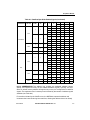
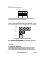
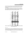
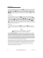
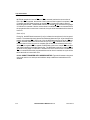
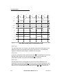
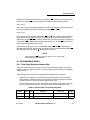
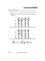
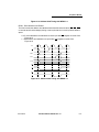
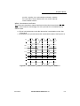
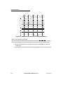
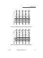
SECTION 8
CHIP-SELECT MODULE
8.1 INTRODUCTION
The Chip-Select module provides user-programmable control of the eight chip-select and
four write-enable outputs. This subsection describes the operation and programming model
of the chip-select registers, including the chip-select address, mask, and control registers.
8.1.1 Features
The following list summarizes the key chip-select features:
¥ Eight programmable chip-select signals
¥ Address masking for memory block sizes from 64k to 2G
¥ Programmable wait states and port sizes
¥ Programmable address setup
¥ Programmable address hold for read and write
¥ Programmable wait states and port sizes for default memory
¥ Alternate master access to chip-selects
8.2 CHIP-SELECT MODULE I/O
8.2.1 Control Signals
The chip-select controller outputs eight chip-select and four write-enable signals. The chipselect controller activates these signals for ColdFire core-initiated transfers as well as during
alternate master-initiated transfers. The chip-select controller can also output transfer
acknowledge during alternate master transfers.
8.2.1.1 CHIP-SELECT (CS[7:0]). These active-low output signals provide control for
peripherals and memory. CS[7:4] are multiplexed with upper address signals (A[27:24]) and
the write-enable (WE[3:0]) signals. CS[0] provides the special function of global chip-select
to let you relocate boot ROM at any defined address space. CS[1] provides the special
function of asserting during CPU space accesses including interrupt acknowledge cycles.
8.2.1.2 WRITE-ENABLE (WE[3:0]). These active-low output signals provide control for
peripherals and memory during write transfers. WE[3:0] are multiplexed with upper address
and upper chip-select signals.
MOTOROLA
MCF5206 USERÕS MANUAL Rev 1.0
8-1
Chip-Select Module
During a write transfers, these outputs indicate which bytes within a long-word transfer are
being selected and which bytes of the data bus will be used for the transfer. WE[0]
controls D[31:24], WE[1] controls D[23:16], WE[2] controls D[15:8] and WE[3] controls
D[7:0]. These signals provide byte data-select signals that are decoded from the SIZx,
A[1:0] signals in addition to the programmed port size and burst capability of the memory
being accessed, as shown in Table 8-1.
Table 8-1. Data Bus Byte Write-Enable Signals
WE[2]
WE[3]
D[31:24] D[23:16] D[15:8]
D[7:0]
WE[0]
TRANSFER SIZE
PORT SIZE
8-BIT
BYTE
16-BIT
32-BIT
BURST
0/1
0/1
0/1
0
SIZ1
0
0
0
0
SIZ0
A1
WE[1]
A0
0
0
0
1
1
1
0
1
0
1
1
1
1
1
0
0
1
1
1
1
1
0
1
1
1
0
0
0
1
1
1
0
1
1
0
1
1
1
1
0
0
1
1
1
1
1
1
0
1
1
0
0
0
1
1
1
0
1
1
0
1
1
1
1
0
1
1
0
1
1
1
1
1
1
0
0
0
0
1
1
1
0
1
0
1
1
1
1
1
0
0
1
1
1
1
1
0
1
1
1
8-BIT
WORD
1
16-BIT
32-BIT
8-2
0/1
0/1
1
1
1
0
0
0
1
1
1
0
1
0
1
1
1
1
0
0
1
1
1
0
1
1
0
1
1
1
0
0
0
0
1
1
0
1
0
0
0
1
1
0
0
0
0
1
1
1
0
1
1
0
0
0
MCF5206 USERÕS MANUAL Rev 1.0
MOTOROLA
Chip-Select Module
Table 8-1. Data Bus Byte Write-Enable Signals (Continued)
WE[2]
WE[3]
D[31:24] D[23:16] D[15:8]
D[7:0]
WE[0]
TRANSFER SIZE
PORT SIZE
BURST
0
SIZ1
0
SIZ0
A1
WE[1]
A0
0
0
0
1
1
1
0
1
0
1
1
1
1
1
0
0
1
1
1
1
1
0
1
1
1
8-BIT
1
0
1
0
0
1
1
1
1
0
1
1
1
0
LONG WORD
0
0
0
1
0
0
1
1
1
1
1
0
1
1
1
0
0
0
0
1
1
1
0
0
0
1
1
0
16-BIT
1
32-BIT
0/1
0
0
0
0
0
0
0
0
1
1
1
0
0
0
1
1
0
0
0
0
0
0
0
0
0
0
0
1
1
1
0
1
0
1
1
1
1
0
0
1
1
1
1
1
1
0
1
1
1
0
0
0
1
1
1
8-BIT
1
1
0
1
0
1
1
1
1
0
0
1
1
1
1
1
0
1
1
1
1
LINE
0
1
0
0
0
0
1
1
1
0
0
0
1
1
0
16-BIT
1
1
0
0
0
0
1
1
1
0
0
0
1
1
1
0
0
0
0
0
0
0
0
0
1
1
1
0
0
0
0
0
0
32-BIT
8.2.1.3 ADDRESS BUS. The address bus includes 24 dedicated address signals,
A[23:0], and supports as many as four additional address signals, A[27:24]. The chipselect or default memory address will appear only on the pins configured to be address
signals. The maximum size of a memory bank is limited by the number of address signals
available (see Table 8-2).
.
For transfers initiated by the ColdFire core, the MCF5206 outputs the address and
increments the lower bits during burst transfers, allowing the address bus to be directly
MOTOROLA
MCF5206 USERÕS MANUAL Rev 1.0
8-3
Chip-Select Module
Table 8-2. Maximum Memory Bank Sizes
AVAILABLE
ADDRESS
SIGNALS
MAXIMUM CS
BANK SIZE
A[23:0]
A[24:0]
A[25:0]
A[26:0]
A[27:0]
16 Mbyte
32 Mbyte
64 Mbyte
128 Mbyte
256 Mbyte
connected to external memory. The MCF5206 does not output the address during
alternate master initiated transfers to chip select memory.
8.2.1.4 DATA BUS. You can configure the chip-select and default memory spaces to be
8-, 16-, or 32-bits wide. A 32-bit port must reside on data bus bits D[31:0], a 16-bit port
must reside on data bus bits D[31:16], and an 8-bit port must reside on data bus bits
D[31:24]. This ensures that the MCF5206 correctly transfers valid data to 8-, 16-, and 32bit ports. Figure 8-1 illustrates the connection of the data bus to 8-, 16-, and 32-bit ports.
EXTERNAL
DATA BUS
D[31:24]
D[23:16]
D[15:8]
D[7:0]
32-BIT PORT
BYTE 0
BYTE 1
BYTE 2
BYTE 3
BYTE 0
BYTE 1
BYTE 2
BYTE 3
16-BIT PORT
BYTE 0
8-BIT PORT
BYTE 1
BYTE 2
BYTE 3
Figure 8-1. MCF5206 Interface to Various Port Sizes
8.2.1.5 TRANSFER ACKNOWLEDGE (TA). Transfer acknowledge is a bidirectional
signal that indicates the current data transfer has been successfully completed. You can
program TA to be output after a programmed number of wait states during alternate
master-initiated transfers that hit in chip-select or default memory address space. TA is
an input during ColdFire core-initiated transfers that hit in chip-select or default memory
address space.
8.3 CHIP-SELECT OPERATION
The chip-select controller provides a glueless interface to certain types of external
memory including PROM and peripherals and external control signals for an easy
interface to SRAM, EPROM, EEPROM and peripherals. Each of the eight chip-select
8-4
MCF5206 USERÕS MANUAL Rev 1.0
MOTOROLA
Chip-Select Module
outputs has an address register, mask register and control register providing individual16bit address decode, 16-bit address masking, port size and burst capability indication, waitstate generation, automatic acknowledge generation as well as address setup and
address hold features.
Chip-selects 0 and 1 provide special functionality. Chip-select 0 is a ÒglobalÓ chip-select
after reset that provides relocatable boot ROM capability. Chip-select 1 can be
programmed to assert during CPU space accesses including interrupt acknowledge
cycles.
The chip-select controller also provides a control register for Òdefault memory,Ó which is
all of the memory space that is not defined by a chip-select or DRAM bank. The default
memory control register lets you program features of the default bus transfer including
port size, burst capability, and wait-state generation.
8.3.1 Chip-Select Bank Definition
The general-purpose chip-selects are controlled by the Chip-select Address Register
(CSAR), Chip-select Mask Register (CSMR), and the Chip-select Control
Register(CSCR). There is one CSAR, one CSMR, and one CSCR for each chip-select
signal generated.
8.3.1.1 BASE ADDRESS AND ADDRESS MASKING. The transfer address generated
by the ColdFire core or by an alternate master is compared to the unmasked bits of the
base address programmed for each chip-select bank in the Chip-Select Address
Registers (CSAR0 - CSAR7). The masked address bits are controlled by the value
programmed in the BAM field in the Chip-Select Mask Registers (CSMR0 - CSMR7).
The masking of address bits defines the address space of the chip-select bank. Address
bits that are masked are not used in the comparison with the transfer address. The base
address field (BA31-BA16) in the CSARs and the base address mask field (BAM31BAM16) in the CSMRs correspond to transfer address bits 31-16. Clearing all bits in the
BAM field makes the address space 64 kbyte. For the address space of a chip-select bank
to be contiguous, address bits should be masked (BAM bits set to a 1) in ascending order
starting with A[16].
NOTE
The MCF5206 compares the address for the current bus
transfer with the address and mask bits in the chip-select
Address Registers (CSARs), DRAM Controller Address
Registers (DCARs), the Chip-Select Mask Registers
MOTOROLA
MCF5206 USERÕS MANUAL Rev 1.0
8-5
Chip-Select Module
(CSMRs), and DRAM Controller Mask Register (DCMRs),
looking for a match.
The priority is listed in Table 8-3 (from highest priority to
lowest priority):
Table 8-3. Chip-select, DRAM and Default Memory Address Decoding Priority
Chip-select 0
Chip-select 1
Chip-select 2
Chip-select 3
Chip-select 4
Chip-select 5
Chip-select 6
Chip-select 7
DRAM Bank 0
DRAM Bank 1
Default Memory
Highest Priority
Lowest Priority
The MCF5206 will compare the address and mask in chipselect 0 - 7 (chip-select 0 is compared first), then the address
and mask in DRAM 0 - 1. If the address does not match in
either or these, the MCF5206 will use the control bits in the
Default Memory Control Register (DMCR) to control the bus
transfer. If the Default Memory Control Register (DMCR)
control bits are used, no chip-select or DRAM control signals
will be asserted during the transfer.
8.3.1.2 ACCESS PERMISSIONS. Chip-select accesses can be restricted based on
transfer direction and attributes. Each chip-select can be enabled for read and/or write
transfers using the WR and RD bits in the CSCRs. Each chip-select can have supervisor
data, supervisor code, user data, user code, and only chip-select 1 can have CPU space
(including interrupt acknowledge) transfers masked from their address space using the
SD, SC, UD, UC, and C/I bits in the CSMRs. The transfer address must match, the
transfer direction must be enabled, and transfer attributes must be unmasked for a chipselect to assert.
8.3.1.3 CONTROL FEATURES. The chip-select control registers and the default
memory control register are used to program timing and assertion features of the chipselect signals. The chip-select control register provides the following programmable
control features:
¥ Port size (8-, 16- or 32-bit)
¥ Number of internal wait states (0 - 15)
¥ Enable assertion of internal transfer acknowledge
¥ Enable assertion of transfer acknowledge for alternate master transfers
8-6
MCF5206 USERÕS MANUAL Rev 1.0
MOTOROLA
Chip-Select Module
¥ Enable burst transfers
¥ Address setup
¥ Address hold
¥ Enable read and/or write transfers
8.3.1.3.1 8-, 16-, and 32-Bit Port Sizing. The general-purpose chip-selects support
static bus sizing. You can program the size of the port controlled by a chip-select. Defined
8 bit ports are connected to D[31:24]; defined 16-bit ports are connected to D[31:16]; and
defined 32 bit ports are connected to D[31:0]. The port size is specified by the PS bits in
the CSCR.
8.3.1.3.2 Termination. The general-purpose chip-selects support three methods of
termination: internal termination, synchronous termination, and asynchronous
termination. You can program the number of wait states required for each chip-select and
the default memory individually. You can also enable internal termination for MCF5206initiated transfers for each chip-select and default memory individually.
Transfer acknowledge (TA) can synchronously terminate a transfer. If the MCF5206
initiates a bus transfer and internal termination is enabled (but TA is asserted before the
specified number of wait states have been inserted), the transfer will terminate on the CLK
cycle where TA is asserted.
NOTE
If an alternate master initiates a bus transfer and internal
termination is enabled, TA should not be driven by an external
device. The MCF5206 will drive TA throughout the alternate
master access.
Asynchronous transfer acknowledge (ATA) can asynchronously terminate a chip-select
or default memory transfer. If the MCF5206 initiates a bus transfer and internal
termination is enabled but ATA is asserted before the specified number of wait states
have been inserted, the transfer will terminate on the CLK cycle where the internal
asynchronous transfer acknowledge is asserted. If an alternate master initiates a bus
transfer and internal termination is enabled, ATA can be driven by an external device to
terminate the transfer before the specified number of wait states has been inserted. In this
case, the transfer will terminate when the internal asynchronous transfer acknowledge is
asserted.
8.3.1.3.3 Bursting Control. The general-purpose chip-selects support burst and nonbursting peripherals and memory. If an external chip-select device cannot be accessed
using burst transfers, you can program the burst-enable bit in the appropriate Chip-Select
Control Register (CSCR) or in the Default Memory Control Register (DMCR) to a 0. If the
burst-enable bit is set to 1, burst transfers will be generated anytime the requested
operand size is greater than the programmed chip-select or default memory port size. If
the burst enable bit is set to 0, nonburst transfers will always be generated for the
MOTOROLA
MCF5206 USERÕS MANUAL Rev 1.0
8-7
Chip-Select Module
particular chip-select or default memory access. Figure 8-5, Figure 8-6, and Figure 8-7
illustrate burst transfers with various settings of address setup, address hold, and 0 wait
states.
8.3.1.3.4 Address Setup and Hold Control. The timing of the assertion and negation of
the general-purpose chip-selects and write-enable signals can be programmed on a chipselect basis. You can program each chip-select to assert when the clock transfer start
(TS) is asserted or assert the CLK cycle after transfer start (TS) is asserted. For burst
transfers, you can select if the chip-select will remain valid while the burst address is
incremented. You can also program the address, attribute, and data (if the transfer is a
write) to remain driven and valid for an additional CLK cycle after the transfer is
terminated. Figure 8-2, Figure 8-3, and Figure 8-4 illustrate three transfers with various
settings.
8.3.2 Global Chip-Select Operation
CS[0] is the global (boot) chip-select and as such, allows address decoding for boot ROM
before system initialization occurs. Its operation differs from the other external chip-select
outputs following a system reset. After system reset, CS[0] is asserted for all accesses
except for CPU space accesses (including MOVEC transfers and interrupt acknowledge
cycles), and internal peripheral accesses. This capability allows the boot ROM to be
located at any address in the external address space. CS[0] operates in this manner until
CSMR0 is written.
The port size and automatic acknowledge functions of CS[0] are determined by the logic
level on pins IRQ1, IRQ4, and IRQ7 sampled on the last rising edge of CLK that RSTI is
asserted (see Bus Operations Section 6.11 Reset Operation).
At system reset, CS[0] allows read and write transfers with address setup, read and write
address-hold enabled, and bursting disabled. Writes to CSCR0 will not deactivate the
global chip-select function; therefore, the number of wait states, read and write enable,
address setup, read and write address hold enable, and burst-enable may be changed.
The global chip-select functionality is disabled on the first write to CSMR0 after reset. You
should set up the appropriate chip-select, DRAM, and default memory control registers
before writing to CSMR0. Once CSMR0 has been written, the global chip-select
functionality can be reactivated only by reset.
8.3.3 General Chip-Select Operation
The MCF5206 uses the address bus (A[28:0]) to specify the location for a data transfer
and the data bus (D[31:0]) to transfer the data. Chip-selects are asserted during bus
transfers where the address, transfer direction and type are not masked for the particular
chip-select. Write-enable signals are asserted on write transfers and indicate the valid
byte lanes for the transfer. Write-enable signals are always asserted on the CLK cycle
after the chip-select is asserted.
8-8
MCF5206 USERÕS MANUAL Rev 1.0
MOTOROLA
Chip-Select Module
Chip-select and write enable signals can be asserted during burst and burst inhibited
transfers. The assertion and negation timing of the chip-select signals are controlled by
the address setup, read address hold, and write address hold bits in the chip-select
control registers.
8.3.3.1 NONBURST TRANSFER WITH NO ADDRESS SETUP AND NO ADDRESS
HOLD. Figure 8-2 illustrates a supervisor data longword write transfer to a 32-bit port. In
this case, address setup and write address hold features are disabled.
.
C1
C2
CLK
TS
A[27:0]
$ADDR
R/W
TT[1:0]
$0
ATM
SIZ[1:0]
$0
D[31:0]
TA
TEA
ATA
CS
WE[3:0]
Figure 8-2. Longword Write Transfer from a 32-Bit Port (No Wait State, No Address
Setup, No Address Hold)
Clock 1 (C1)
The write cycle starts in C1. During C1, the MCF5206 places valid values on the address
bus (A[27:0]) and transfer control signals. The transfer type (TT[1:0]) signals identify the
specific access type and access type and mode (ATM) is driven low to identify the transfer
as data. The read/write (R/W) signal is driven low for a write cycle, and the size signals
MOTOROLA
MCF5206 USERÕS MANUAL Rev 1.0
8-9
Chip-Select Module
(SIZ[1:0]) are driven low to indicate a longword transfer. The MCF5206 asserts transfer
start (TS) to indicate the beginning of a bus cycle and asserts the appropriate chip-select
(CS) for the address being accessed.
Clock 2 (C2)
During C2, the MCF5206 negates transfer start (TS), drives access type and mode (ATM)
high to identify the transfer as supervisor and drives data onto D[31:0]. If the selected
device(s) is ready to latch the data, it latches D[31:0] and asserts the transfer
acknowledge (TA). At the end of C2, the MCF5206 samples the level of TA. If TA is
asserted, the transfer of the longword is complete, and the MCF5206 negates CS and
WE[3:0] after the next rising edge of CLK. If TA is negated, the MCF5206 continues to
sample TA and inserts wait states instead of terminating the transfer. The MCF5206
continues to sample TA on successive rising edge of CLK until it is asserted. If the bus
monitor timer is enabled and TA is not asserted before the programmed bus monitor time
is reached, the cycle will be terminated with an internal bus error.
8.3.3.2 NONBURST TRANSFER WITH ADDRESS SETUP. Figure 8-3 illustrates a
word user data write transfer to a 16-bit port with address setup enabled.
8-10
MCF5206 USERÕS MANUAL Rev 1.0
MOTOROLA
Chip-Select Module
.
C1
C2
C3
CLK
TS
A[27:0]
$ADDR
R/W
TT[1:0]
$0
ATM
SIZ[1:0]
$2
D[31:16]
TA
TEA
ATA
CS
WE[1:0]
WE[3:2]
ADDRESS
SETUP
WAIT
STATE
Figure 8-3. Word Write Transfer to a 16-Bit Port (One Wait State, Address Setup, No
Address Hold)
Clock 1 (C1)
The write cycle starts in C1. During C1, the MCF5206 places valid values on the address
bus (A[27:0]) and transfer control signals. The transfer type (TT[1:0]) signals identify the
specific access type and access type and mode (ATM) is driven low to identify the transfer
as data. The read/write (R/W) signal is driven low for a write cycle, and the size signals
(SIZ[1:0]) are driven to $2 to indicate a word transfer. The MCF5206 asserts transfer start
(TS) to indicate the beginning of a bus cycle. The chip-select (CS) signal is driven high
since the appropriate address setup bit in the chip-select control register is set to 1.
MOTOROLA
MCF5206 USERÕS MANUAL Rev 1.0
8-11
Chip-Select Module
Clock 2 (C2)
During C2, the MCF5206 negates transfer start (TS), drives access type and mode (ATM)
low to identify the transfer as user and drives data onto D[31:16] and asserts the
appropriate chip-select (CS) signal. At the end of C2, the MCF5206 samples the level of
TA. If TA was asserted the transfer of the word would be complete. Since TA is negated,
the MCF5206 continues to output the data and inserts a wait state instead of terminating
the transfer.
Clock 3 (C3)
The MCF5206 asserts the write enable (WE[1:0]) signals. If the selected device(s) is
ready to latch the data, it latches D[31:0] and asserts the transfer acknowledge (TA). At
the end of C3, the MCF5206 samples the level of TA . If TA is asserted, the transfer of the
word is complete, and the MCF5206 negates CS and WE[1:0] after the rising edge of
CLK. If TA is negated, the MCF5206 continues to sample TA and inserts wait states
instead of terminating the transfer. The MCF5206 continues to sample TA on successive
rising edge of CLK until it is asserted. If the bus monitor timer is enabled and TA is not
asserted before the programmed bus monitor time is reached, the cycle will be terminated
with an internal bus error.
NOTE
When address setup is enabled (ASET=1), write-enables
(WE[3:0]) will not assert on zero wait state write transfers.
8.3.3.3 NONBURST TRANSFER WITH ADDRESS SETUP AND HOLD. Figure 8-4
illustrates a supervisor data byte write transfer to an 8-bit port with address setup and
write address hold enabled.
8-12
MCF5206 USERÕS MANUAL Rev 1.0
MOTOROLA
Chip-Select Module
.
C1
C2
C3
C4
CLK
TS
A[27:0]
$ADDR
R/W
TT[1:0]
$0
ATM
SIZ[1:0]
$1
D[31:16]
TA
TEA
ATA
CS
WE[0]
WE[3:1]
ADDRESS
SETUP
WAIT
STATE
ADDRESS
HOLD
Figure 8-4. Byte Write Transfer from an 8-Bit Port (One Wait State, Address Setup,
Address Hold)
Clock 1 (C1)
The write cycle starts in C1. During C1, the MCF5206 places valid values on the address
bus (A[27:0]) and transfer control signals. The transfer type (TT[1:0]) signals identify the
specific access type and access type and mode (ATM) is driven low to identify the transfer
as data. The read/write (R/W) signal is driven low for a write cycle, and the size signals
(SIZ[1:0]) are driven to $1 to indicate a byte transfer. The MCF5206 asserts transfer start
(TS) to indicate the beginning of a bus cycle. The chip-select (CS) signal is driven high
since the appropriate address setup bit in the chip-select control register is set to 1.
Clock 2 (C2)
MOTOROLA
MCF5206 USERÕS MANUAL Rev 1.0
8-13
Chip-Select Module
During C2, the MCF5206 negates transfer start (TS), drives access type and mode (ATM)
high to identify if the transfer as supervisor, drives data onto D[31:16] and asserts the
appropriate chip-select (CS) signal. At the end of C2, the MCF5206 samples the level of
TA. If TA was asserted the transfer of the word would be complete. Since TA is negated,
the MCF5206 continues to output the data and inserts a wait state instead of terminating
the transfer.
Clock 3 (C3)
The MCF5206 asserts the write enable (WE[1:0]) signals. If the selected device(s) is
ready to latch the data, it latches D[31:0] and asserts the transfer acknowledge (TA). At
the end of C3, the MCF5206 samples the level of TA. If TA is asserted, the transfer of the
word is complete. If TA is negated, the MCF5206 continues to sample TA and inserts wait
states instead of terminating the transfer. The MCF5206 continues to sample TA on
successive rising edge of CLK until it is asserted. If the bus monitor timer is enabled and
TA is not asserted before the programmed bus monitor time is reached, the cycle will be
terminated with an internal bus error.
Clock 4 (C4)
The MCF5206 negates the chip-select (CS) and write enable (WE[1:0]) signals and
continues to drive the address, data and attribute signals until after the next rising edge
of CLK.
NOTE
When address setup is enabled (ASET=1), write enables
(WE[3:0]) will not assert on zero wait state write transfers.
8.3.3.4 BURST TRANSFER. If the burst enable bit in the appropriate control register
(Chip-select Control Register or Default Memory Control Register) is set to 1, and the
operand size is larger than the port size of the memory being accessed, the MCF5206
performs word, longword and line transfers in burst mode. When burst mode is selected,
the size of the transfer (indicated by SIZ[1:0]) will reflect the size of the operand being read
- not the size of the port being accessed (i.e. a line transfer will be indicated by SIZ[1:0] =
$3 and a longword transfer will be indicated by SIZ[1:0] = $0, regardless of the size of the
port or the number of transfers required to access the data).
The MCF5206 supports burst-inhibited transfers for memory devices that are unable to
support bursting. For this type of bus cycle, the burst enable bit in the Chip-select Control
Registers (CSCRs) or Default Memory Control Register (DMCR) must be cleared.
Figure 8-5 illustrates a supervisor code longword read transfer to a 16-bit port with
address setup and address hold disabled.
8-14
MCF5206 USERÕS MANUAL Rev 1.0
MOTOROLA
Chip-Select Module
.
C1
C2
C3
CLK
TS
A[27:0]
$ADDR
$ADDR + 2
R/W
TT[1:0]
$0
ATM
SIZ[1:0]
$0
D[31:16]
TA
TEA
ATA
CS
WE[3:0]
Figure 8-5. Longword Burst Read Transfer from a 16-Bit Port (No Wait States,
No Address Setup, No Address Hold)
Clock 1 (C1)
The burst read cycle starts in C1. During C1, the MCF5206 places valid values on the
address bus (A[27:0]) and transfer control signals. The transfer type (TT[1:0]) signals
identify the specific access type and access type and mode (ATM) is driven high to identify
the transfer as code. The read/write (R/W) and write enable (WE[3:0]) signals are driven
high for a read cycle, and the size signals (SIZ[1:0]) are driven low to indicate a longword
transfer. The MCF5206 asserts transfer start (TS) to indicate the beginning of a bus cycle
and asserts the appropriate chip-select (CS) for the address being accessed.
Clock 2 (C2)
During C2, the MCF5206 negates transfer start (TS), drives access type and mode (ATM)
high to identify the transfer as supervisor. The selected device(s) places the addressed
data onto D[31:16] and asserts the transfer acknowledge (TA). At the end of C2, the
MOTOROLA
MCF5206 USERÕS MANUAL Rev 1.0
8-15
Chip-Select Module
MCF5206 samples the level of TA and if TA is asserted, latches the current value of
D[31:16]. If TA is asserted, the transfer of the first word of the longword is complete. If TA
is negated, the MCF5206 continues to sample TA and inserts wait states instead of
terminating the transfer. The MCF5206 continues to sample TA on successive rising edge
of CLK until it is asserted. If the bus monitor timer is enabled and TA is not asserted before
the programmed bus monitor time is reached, the cycle will be terminated with an internal
bus error.
Clock 3 (C3)
During C3, the MCF5206 increments A[1:0] to indicate the second word in the longword
transfer. The selected device(s) places the addressed data onto D[31:16] and asserts the
transfer acknowledge (TA). At the end of C3, the MCF5206 samples the level of TA and
if TA is asserted, latches the current value of D[31:16]. If TA is asserted, the transfer of
the second word of the longword is complete and the transfer terminates and the chipselect (CS) is negated. If TA is negated, the MCF5206 continues to sample TA and inserts
wait states instead of terminating the transfer. The MCF5206 continues to sample TA on
successive rising edge of CLK until it is asserted. If the bus monitor timer is enabled and
TA is not asserted before the programmed bus monitor time is reached, the cycle will be
terminated with an internal bus error.
8.3.3.5 BURST TRANSFER WITH ADDRESS SETUP. Figure 8-6 illustrates a longword
user code read from a 16-bit port with address setup enabled and read address hold
disabled.
8-16
MCF5206 USERÕS MANUAL Rev 1.0
MOTOROLA
Chip-Select Module
.
C1
C2
C3
C4
CLK
TS
A[27:0]
$ADDR
$ADDR + 2
R/W
TT[1:0]
$0
ATM
SIZ[1:0]
$0
D[31:16]
TA
TEA
ATA
CS
WE[3:0]
ADDRESS
SETUP
ADDRESS
SETUP
Figure 8-6. Longword Burst Read Transfer from a 16-Bit Port (No Wait States,
Address Setup, No Address Hold)
Clock 1 (C1)
The burst read cycle starts in C1. During C1, the MCF5206 places valid values on the
address bus (A[27:0]) and transfer control signals. The transfer type (TT[1:0]) signals
identify the specific access type and access type and mode (ATM) is driven high to identify
the transfer as reading code. The read/write (R/W) and write enable (WE[3:0]) signals are
driven high for a read cycle, and the size signals (SIZ[1:0]) are driven low to indicate a
longword transfer. The MCF5206 asserts transfer start (TS) to indicate the beginning of a
bus cycle. The chip-select (CS) signal is driven high since the appropriate address setup
bit in the chip-select control register is set to 1.
MOTOROLA
MCF5206 USERÕS MANUAL Rev 1.0
8-17
Chip-Select Module
Clock 2 (C2)
During C2, the MCF5206 negates transfer start (TS), drives access type and mode (ATM)
low to identify if the transfer as user. The appropriate chip-select (CS) signal is asserted.
The selected device(s) places the addressed data onto D[31:16] and asserts the transfer
acknowledge (TA). At the end of C2, the MCF5206 samples the level of TA and if TA is
asserted, latches the current value of D[31:16]. If TA is asserted, the transfer of the first
word of the longword is complete and chip-select (CS) is negated after the next rising
edge of CLK. If TA is negated, the MCF5206 continues to sample TA and inserts wait
states instead of terminating the transfer. The MCF5206 continues to sample TA on
successive rising edge of CLK until it is asserted. If the bus monitor timer is enabled and
TA is not asserted before the programmed bus monitor time is reached, the cycle will be
terminated with an internal bus error.
Clock 3 (C3)
During C3, the MCF5206 increments A[1:0] to indicate the second word in the longword
transfer. The chip-select (CS) signal is driven high since the appropriate address setup bit
in the chip-select control register is set to 1.
Clock 4 (C4)
The selected device(s) places the addressed data onto D[31:16] and asserts the transfer
acknowledge (TA). At the end of C4, the MCF5206 samples the level of TA and if TA is
asserted, latches the current value of D[31:16]. If TA is asserted, the transfer of the
second word of the longword is complete and the transfer terminates and the chip-select
(CS) is negated. If TA is negated, the MCF5206 continues to sample TA and inserts wait
states instead of terminating the transfer. The MCF5206 continues to sample TA on
successive rising edge of CLK until it is asserted. If the bus monitor timer is enabled and
TA is not asserted before the programmed bus monitor time is reached, the cycle will be
terminated with an internal bus error.
NOTE
When address setup is enabled (ASET=1), write enables
(WE[3:0]) will not assert on zero wait state write transfers.
8.3.3.6 BURST TRANSFER WITH ADDRESS SETUP AND HOLD. Figure 8-7
illustrates a supervisor data word read transfer from an 8-bit port with address setup and
read address hold enabled.
8-18
MCF5206 USERÕS MANUAL Rev 1.0
MOTOROLA
Chip-Select Module
.
C1
C2
C3
C4
C5
C6
CLK
TS
A[27:0]
$ADDR
$ADDR + 1
R/W
TT[1:0]
$0
ATM
SIZ[1:0]
$2
D[31:24]
TA
TEA
ATA
CS
WE[3:0]
ADDRESS
SETUP
ADDRESS
HOLD
Figure 8-7. Word Burst Read Transfer from an 8-Bit Port (No Wait States, Address
Setup, Address Hold)
Clock 1 (C1)
The burst read cycle starts in C1. During C1, the MCF5206 places valid values on the
address bus (A[27:0]) and transfer control signals. The transfer type (TT[1:0]) signals
identify the specific access type and access type and mode (ATM) is driven low to identify
the transfer as reading data. The read/write (R/W) and write enable (WE[3:0]) signals are
driven high for a read cycle, and the size signals (SIZ[1:0]) are driven to $2 to indicate a
word transfer. The MCF5206 asserts transfer start (TS) to indicate the beginning of a bus
cycle. The chip-select (CS) signal is driven high since the appropriate address setup bit
in the chip-select control register is set to 1.
MOTOROLA
MCF5206 USERÕS MANUAL Rev 1.0
8-19
Chip-Select Module
Clock 2 (C2)
During C2, the MCF5206 negates transfer start (TS), drives access type and mode (ATM)
high to identify the transfer as supervisor. The appropriate chip-select (CS) signal is
asserted. The selected device(s) places the addressed data onto D[31:24] and asserts
the transfer acknowledge (TA). At the end of C2, the MCF5206 samples the level of TA
and if TA is asserted, latches the current value of D[31:24]. If TA is asserted, the transfer
of the first byte of the word is complete and chip-select (CS) is negated after the next rising
edge of CLK. If TA is negated, the MCF5206 continues to sample TA and inserts wait
states instead of terminating the transfer. The MCF5206 continues to sample TA on
successive rising edge of CLK until it is asserted. If the bus monitor timer is enabled and
TA is not asserted before the programmed bus monitor time is reached, the cycle will be
terminated with an internal bus error.
Clock 3 (C3)
The MCF5206 continues to drive address and bus attributes since the read address hold
bit in the appropriate chip-select control register is set to 1.
Clock 4(C4)
During C3, the MCF5206 increments A[0] to indicate the second byte in the word transfer.
The chip-select (CS) signal is driven high since the appropriate address setup bit in the
chip-select control register is set to 1.
Clock 5(C5)
The selected device(s) places the addressed data onto D[31:24] and asserts the transfer
acknowledge (TA). At the end of C5, the MCF5206 samples the level of TA and if TA is
asserted, latches the current value of D[31:24]. If TA is asserted, the transfer of the
second word of the longword is complete and the transfer terminates and the chip-select
(CS) is negated. If TA is negated, the MCF5206 continues to sample TA and inserts wait
states instead of terminating the transfer. The MCF5206 continues to sample TA on
successive rising edge of CLK until it is asserted. If the bus monitor timer is enabled and
TA is not asserted before the programmed bus monitor time is reached, the cycle will be
terminated with an internal bus error.
Clock 6 (C6)
The MCF5206 continues to drive address and bus attributes since the read address hold
bit in the appropriate chip-select control register is set to 1.
NOTE
When address setup is enabled (ASET=1), write enables
(WE[3:0]) will not assert on zero wait state write transfers.
8-20
MCF5206 USERÕS MANUAL Rev 1.0
MOTOROLA
Chip-Select Module
8.3.4 Alternate Master Chip-Select Operation
The MCF5206 can monitor bus transfers by other bus masters and assert chip-select and
transfer termination signals during these transfers. Assertion of chip-select and
termination signals will occur when the bus is granted to another bus master and TS is
asserted by the alternate master as an input to the MCF5206. The MCF5206 registers the
value of A[27:0], R/W and SIZ[1:0] on the rising edge of CLK in which TS is asserted.
NOTE
If the pins A[27:24]/CS[7:4]/WE[0:3] are not assigned to
output address signals, a value of $0 is assigned internally to
these signals. Also, TT[1:0] and ATM are not examined during
alternate master transfers. The mask bits: SC, SD, UC, UD,
and C/I in the Chip-select Mask Registers (CSMR) are not
used during alternate master transfers.
The MCF5206 examines the address, direction and size of the transfer and on the next
rising edge of CLK, begins assertion of the proper sequence of memory control signals. If
the transfer is decoded to be a chip-select address and the chip-select is enabled for the
direction of the transfer (read and/or write enabled), the appropriate chip-select and write
enable signals will be asserted. If the chip-select is enabled for alternate master automatic
acknowledge, TA will be driven and asserted at the appropriate time. The MCF5206 does
not drive address during external bus master accesses that are decoded as chip-select or
default memory transfers. The alternate master must provide the correct address to the
external memory at the appropriate time.
If the address of the transfer is neither a chip-select or a DRAM address, the SIM will read
the Default Memory Control Register (DMCR). If the alternate master automatic
acknowledge (EMAA) bit in the DMCR is set, the MCF5206 will drive transfer
acknowledge (TA) as an output and will assert transfer acknowledge after the number of
clocks programmed in the wait state bits (WS) in the DMCR.
8.3.4.1 ALTERNATE MASTER NONBURST TRANSFER. The general-purpose chipselects support burst and nonbursting peripherals and memory for alternate master
accesses. If an external chip-select device can not be accessed using burst transfers, you
can program the burst-enable bit in the appropriate Chip-Select Control Register (CSCR)
or in the DMCR to 0. If the burst-enable bit is set to 1, and the alternate master initiates a
transfer where the transfer size is greater than the programmed port size, the MCF5206
will assert the chip-select control signals for a burst transfer. If the burst enable bit is set
to 0, the alternate master should never initiate a transfer with the size specified as larger
than the programmed port size. Figure 8-8 illustrates a longword read transfer initiated by
an alternate master to a 32-bit port.
MOTOROLA
MCF5206 USERÕS MANUAL Rev 1.0
8-21
Chip-Select Module
.
C1
C2
C3
C4
CLK
TS
A[27:0]
$ADDR
R/W
SIZ[1:0]
$0
D[31:0]
TA
TEA
ATA
CS
WE[3:0]
Figure 8-8. Alternate Master Longword Read Transfer from a 32-Bit Port (No Wait
State, No Address Setup, No Address Hold)
Clock 1 (C1)
The write cycle starts in C1. During C1, the alternate master places valid values on the
address bus (A[27:0]) and transfer control signals. The MCF5206 registers the alternate
master address, read/write and size signals.
Clock 2 (C2)
During C2, the alternate master negates transfer start (TS). The MCF5206 compares the
alternate master address to the internal chip-select addresses and enables the
appropriate chip-select for assertion.
Clock 3 (C3)
The MCF5206 asserts the appropriate chip-select and since the EMAA bit in the
appropriate Chip-select Control Register (CSCR) is set to one, asserts transfer
acknowledge (TA). The selected device drive data onto D[31:0]. At the end of C3, the
alternate master samples the level of TA. If TA is asserted, the transfer of the longword is
8-22
MCF5206 USERÕS MANUAL Rev 1.0
MOTOROLA
Chip-Select Module
complete. If TA is negated, the alternate master continues to sample TA and inserts wait
states instead of terminating the transfer.
Clock 4 (C4)
At the start of clock 4, the MCF5206 negates CS and TA, completing the alternate master
transfer. After the next rising edge of CLK, the MCF5206 three states TA. The alternate
master can assert TS starting another transfer.
8.3.4.2 ALTERNATE MASTER BURST TRANSFER. The timing of the assertion and
negation of the general-purpose chip-selects and write-enable signals during alternate
master accesses can be programmed on a chip-select basis. The address setup and hold
features of the chip-selects are not used during nonburst alternate master accesses. The
address setup and hold features can insert CLK cycles where the chip-select is negated,
during burst cycles. During alternate master read transfers, the MCF5206 will drive the
activated chip-select signal negated for one CLK cycle for each of the address setup and
read address hold bits that are set to 1. During alternate master write transfers, the
MCF5206 will drive the activated chip-select signal negated for one CLK cycle for each of
the address setup and write address hold bits that are set to 1. Figure 8-9 illustrates a
bursting longword read transfer from a 16-bit port with no address setup and no address
hold.
MOTOROLA
MCF5206 USERÕS MANUAL Rev 1.0
8-23
Chip-Select Module
.
C1
C2
C3
C4
C5
CLK
TS
A[27:0]
$ADDR
$ADDR + 2
R/W
SIZ[1:0]
$0
D[31:16]
TA
TEA
ATA
CS
WE[3:0]
Figure 8-9. Alternate Master Longword Read Transfer from a 16-bit Port (No Wait
State, No Address Setup, No Address Hold)
Clock 1 (C1)
The read cycle starts in C1. During C1, the alternate master places valid values on the
address bus (A[27:0]) and transfer control signals. At the end of C1, the MCF5206
registers the alternate master address, read/write and size signals.
Clock 2 (C2)
During C2, the alternate master negates transfer start (TS). The MCF5206 compares the
alternate master address to the internal chip-select addresses and enables the
appropriate chip-select and transfer acknowledge (TA) for assertion.
Clock 3 (C3)
The MCF5206 asserts the appropriate chip-select and since the EMAA bit in the
appropriate Chip-select Control Register (CSCR) is set to one and wait states are set to
zero, asserts transfer acknowledge (TA). The selected device drives data onto D[31:16].
At the end of C3, the alternate master samples the level of TA. If TA is asserted, the
8-24
MCF5206 USERÕS MANUAL Rev 1.0
MOTOROLA
Chip-Select Module
transfer of the first word of the longword is complete. If TA is negated, the alternate master
continues to sample TA and inserts wait states instead of terminating the transfer.
Clock 4 (C4)
At the start of clock 4, the alternate master increments the address to indicate the second
word of the longword transfer. The MCF5206 continues to assert CS and TA and the
selected slave outputs the data indicated by the new address on D[31:16]. At the end of
clock 4, the alternate master samples the level of TA. If TA is asserted, the transfer of the
second word of the longword is complete. If TA is negated, the alternate master continues
to sample TA and inserts wait states instead of terminating the transfer.
Clock 5 (C5)
At the start of clock 5, the MCF5206 negates CS and TA, completing the alternate master
transfer. After the next rising edge of CLK, the MCF5206 three states TA. The alternate
master can assert TS starting another transfer.
NOTE
Write enables (WE[3:0]) will not assert on zero wait state
alternate master write transfers.
8.3.4.3 ALTERNATE MASTER BURST TRANSFER WITH ADDRESS SETUP AND
HOLD. Figure 8-10 illustrates a longword bursting read transfer from a 16-bit port with
either address setup or read address hold enabled.
MOTOROLA
MCF5206 USERÕS MANUAL Rev 1.0
8-25
Chip-Select Module
.
C1
C2
C3
C4
C5
CLK
TS
A[27:0]
$ADDR
$ADDR + 2
R/W
SIZ[1:0]
$0
D[31:16]
TA
TEA
ATA
CS
WE[3:0]
Figure 8-10. Alternate Master Longword Read Transfer from a 16-Bit Port (No Wait
State, With Address Setup Or Read Address Hold)
Clock 1 (C1)
The read cycle starts in C1. During C1, the alternate master places valid values on the
address bus (A[27:0]) and transfer control signals. At the end of C1, the MCF5206
registers the alternate master address, read/write and size signals.
Clock 2 (C2)
During C2, the alternate master negates transfer start (TS). The MCF5206 compares the
alternate master address to the internal chip-select addresses and enables the
appropriate chip-select and transfer acknowledge (TA) for assertion.
Clock 3 (C3)
The MCF5206 asserts the appropriate chip-select and since the EMAA bit in the
appropriate Chip-select Control Register (CSCR) is set to one and wait states are set to
zero, asserts transfer acknowledge (TA). The selected device drives data onto D[31:16].
At the end of C3, the alternate master samples the level of TA. If TA is asserted, the
8-26
MCF5206 USERÕS MANUAL Rev 1.0
MOTOROLA
Chip-Select Module
transfer of the first word of the longword is complete. If TA is negated, the alternate master
continues to sample TA and inserts wait states instead of terminating the transfer.
Clock 4 (C4)
At the start of clock 4, the alternate master increments the address to indicate the second
word of the longword transfer. The MCF5206 negates CS and TA.
Clock 5 (C5)
At the start of clock 5, the MCF5206 asserts CS and TA. The selected slave outputs the
data indicated by the address on D[31:16]. At the end of clock 4, the alternate master
samples the level of TA. If TA is asserted, the transfer of the second word of the longword
is complete. If TA is negated, the alternate master continues to sample TA and inserts wait
states instead of terminating the transfer.
After the next rising edge of CLK, the MCF5206 negates CS and TA, completing the
alternate master transfer. After the next rising edge of CLK, the MCF5206 three states TA.
The alternate master can assert TS starting another transfer.
NOTE
Write enables (WE[3:0]) will not assert on zero wait state
alternate master write transfers.
8.4 PROGRAMMING MODEL
8.4.1 Chip-Select Registers Memory Map
Table 8-4 shows the memory map of all the chip-select module registers. The internal
registers in the chip-select module are memory-mapped registers offset from the MBAR
address pointer.
The following lists several keynotes regarding the programming model table:
¥ Addresses not assigned to a register and undefined register bits are reserved for
future expansion. Write accesses to these reserved address spaces and reserved
register bits have no effect; read accesses will return zeros.
¥ The reset value column indicates the register initial value at reset. Certain registers
may be uninitialized at reset, i.e., they may contain random values after reset.
Table 8-4. Memory Map of Chip-Select Registers
ADDRESS
NAME
WIDTH
DESCRIPTION
RESET VALUE
ACCESS
MBAR +$ 64
CSAR0
16
Chip-Select Address Register - Bank 0
0000
R/W
MBAR +$ 68
CSMR0
32
Chip-Select Mask Register - Bank 0
00000000
R/W
MOTOROLA
MCF5206 USERÕS MANUAL Rev 1.0
8-27
Chip-Select Module
Table 8-4. Memory Map of Chip-Select Registers (Continued)
ADDRESS
NAME
WIDTH
DESCRIPTION
RESET VALUE
ACCESS
MBAR + $6E
CSCR0
16
Chip-Select Control Register - Bank 0
3C1F, 3C5F, 3C9F, 3CDF, 3D1F,
3D5F, 3D9F, or 3DDF
AA set by IRQ7 at reset
PS1 set by IRQ4 at reset
PS0 set by IRQ1 at reset
MBAR + $70
CSAR1
16
Chip-Select Address Register - Bank 1
uninitialized
R/W
MBAR + $74
CSMR1
32
Chip-Select Mask Register - Bank 1
uninitialized
R/W
MBAR + $7A
CSCR1
16
Chip-Select Control Register - Bank 1
uninitialized
(except
R/W
BRST=ASET=WRAH=RDAH=WR=R
D=0)
MBAR + $7C
CSAR2
16
Chip-Select Address Register - Bank 2
uninitialized
R/W
MBAR + $80
CSMR2
32
Chip-Select Mask Register - Bank 2
uninitialized
R/W
MBAR + $86
CSCR2
16
Chip-Select Control Register - Bank 2
uninitialized
(except
R/W
BRST=ASET=WRAH=RDAH=WR=R
D=0)
MBAR + $88
CSAR3
16
Chip-Select Address Register - Bank 3
uninitialized
R/W
MBAR + $8C
CSMR3
32
Chip-Select Mask Register - Bank 3
uninitialized
R/W
MBAR + $92
CSCR3
16
Chip-Select Control Register - Bank 3
uninitialized
(except
R/W
BRST=ASET=WRAH=RDAH=WR=R
D=0)
MBAR + $94
CSAR4
16
Chip-Select Address Register - Bank 4
uninitialized
R/W
MBAR +$ 98
CSMR4
32
Chip-Select Mask Register - Bank 4
uninitialized
R/W
MBAR +$ 9E
CSCR4
16
Chip-Select Control Register - Bank 4
uninitialized
(except
R/W
BRST=ASET=WRAH=RDAH=WR=R
D=0)
MBAR + $A0
CSAR5
16
Chip-Select Address Register - Bank 5
uninitialized
R/W
MBAR + $A4
CSMR5
32
Chip-Select Mask Register - Bank 5
uninitialized
R/W
MBAR + $AA
CSCR5
16
Chip-Select Control Register - Bank 5
uninitialized
(except
R/W
BRST=ASET=WRAH=RDAH=WR=R
D=0)
MBAR + $AC
CSAR6
16
Chip-Select Address Register - Bank 6
uninitialized
R/W
MBAR + $B0
CSMR6
32
Chip-Select Mask Register - Bank 6
uninitialized
R/W
MBAR + $B6
CSCR6
16
Chip-Select Control Register - Bank 6
uninitialized
(except
R/W
BRST=ASET=WRAH=RDAH=WR=R
D=0)
8-28
MCF5206 USERÕS MANUAL Rev 1.0
R/W
MOTOROLA
Chip-Select Module
Table 8-4. Memory Map of Chip-Select Registers (Continued)
ADDRESS
NAME
WIDTH
DESCRIPTION
RESET VALUE
ACCESS
MBAR +$ B8
CSAR7
16
Chip-Select Address Register - Bank 7
uninitialized
R/W
MBAR + $BC
CSMR7
32
Chip-Select Mask Register - Bank 7
uninitialized
R/W
MBAR +$ C2
CSCR7
16
Chip-Select Control Register - Bank 7
uninitialized
(except
R/W
BRST=ASET=WRAH=RDAH=WR=R
D=0)
MBAR + $C6
DMCR
16
Default Memory Control Register
0000
R/W
8.4.2 Chip-Select Controller Registers
8.4.2.1 CHIP-SELECT ADDRESS REGISTER (CSAR0 - CSAR7). Each CSAR
determines the base address of the corresponding chip-select pin.
Each CSAR is a 16-bit read/write register. CSAR0 is initialized to $0000 at reset and
CSAR1-CSAR7 are unaffected (uninitialized) by reset.
.
MBAR + $64
Chip-Select Address Register(CSAR0)
15
14
13
12
11
10
9
8
7
6
5
4
3
2
1
0
BA31
BA30
BA29
BA28
BA27
BA26
BA25
BA24
BA23
BA22
BA21
BA20
BA19
BA18
BA17
BA16
0
0
0
0
0
0
0
0
0
0
0
0
0
0
0
RESET:
0
.
Chip-select Address Register (CSAR1 - CSAR7)
15
14
13
12
11
10
9
8
7
6
5
4
3
2
1
0
BA31
BA30
BA29
BA28
BA27
BA26
BA25
BA24
BA23
BA22
BA21
BA20
BA19
BA18
BA17
BA16
-
-
-
-
-
-
-
-
-
-
-
-
-
-
-
RESET:
-
BA31-BA16 - Base Address
This field defines the base address location of memory dedicated to each chip-select.
These bits are compared to ColdFire core address bus bits 31-16 to determine if the chipselect memory is being accessed. During alternate master accesses these bits are
compared as shown in Table 8-5.
Table 8-5. BA Field Comparisons for Alternate Master Transfers
BA BIT
COMPARED TO
CONDITIONS
BA31 - BA28
$0
$0
A[27]
$0
A[26]
Always
A[27]/CS[7]/WE[0] does not output A[27]
A[27]/CS[7]/WE[0] outputs A[27]
A[26]/CS[6]/WE[1] does not output A[26]
A[26]/CS[6]/WE[1] outputs A[26]
BA27
BA26
MOTOROLA
MCF5206 USERÕS MANUAL Rev 1.0
8-29
Chip-Select Module
Table 8-5. BA Field Comparisons for Alternate Master Transfers (Continued)
BA BIT
COMPARED TO
CONDITIONS
$0
A[25]
$0
A[24]
A[23:16]
A[25]/CS[5]/WE[2] does not output A[25]
A[25]/CS[5]/WE2 outputs A[25]
A[24]/CS[4]/WE[3] does not output A[24]
A[24]/CS[4]/WE[3] outputs A[24]
Always
BA25
BA24
BA23 - BA16
8.4.2.2 CHIP-SELECT MASK REGISTER (CSMR0 - CSMR7). Each CSMR determines
the address mask for each of the chip-selects as well the definition of which types of
accesses are allowed for these signals. Each CSMR is a 32-bit read/write control register.
CSMR0 is initialized to $00000000 by reset and CSMR7 - CSMR1 are unaffected
(uninitialized) by reset. At reset, CS[0] is activated as the global chip-select. A write to
CSMR0 deactivates this function. CSMR1 has an additional control bit CPU that allows
you to mask CPU space (including interrupt acknowledge) transfers.
MBAR +$68
Chip-Select Mask Register(CSMR0)
31
30
29
28
27
26
25
24
23
22
21
20
19
18
17
16
BAM31 BAM30 BAM29 BAM28 BAM27 BAM26 BAM25 BAM24 BAM23 BAM22 BAM21 BAM20 BAM19 BAM18 BAM17 BAM16
RESET:
0
0
0
0
0
0
0
0
0
0
0
0
0
0
0
0
15
14
13
12
11
10
9
8
7
6
5
4
3
2
1
0
-
-
-
-
-
-
-
-
-
-
-
SC
SD
UC
UD
-
0
0
0
0
0
0
0
0
0*
0
0
0
0
0
0
27
26
25
24
23
22
21
20
19
18
RESET:
0
MBAR +$74
Chip-Select Mask Register(CSMR1)
31
30
29
28
17
16
BAM31 BAM30 BAM29 BAM28 BAM27 BAM26 BAM25 BAM24 BAM23 BAM22 BAM21 BAM20 BAM19 BAM18 BAM17 BAM16
RESET:
-
-
-
-
-
-
-
-
-
-
-
-
-
-
-
-
15
14
13
12
11
10
9
8
7
6
5
4
3
2
1
0
-
-
-
-
-
-
-
-
-
-
C/I
SC
SD
UC
UD
-
0
0
0
0
0
0
0
0
0
-
-
-
-
-
0
RESET:
0
8-30
MCF5206 USERÕS MANUAL Rev 1.0
MOTOROLA
Chip-Select Module
Chip-Select Mask Register(CSMR2 - CSMR7)
31
30
29
28
27
26
25
24
23
22
21
20
19
18
17
16
BAM31 BAM30 BAM29 BAM28 BAM27 BAM26 BAM25 BAM24 BAM23 BAM22 BAM21 BAM20 BAM19 BAM18 BAM17 BAM16
RESET:
-
-
-
-
-
-
-
-
-
-
-
-
-
-
-
-
15
14
13
12
11
10
9
8
7
6
5
4
3
2
1
0
-
-
-
-
-
-
-
-
-
-
-
SC
SD
UC
UD
-
0
0
0
0
0
0
0
0
0
0
-
-
-
-
0
RESET:
0
BAM31-BAM16 - Base Address Mask
This field defines the chip-select block size through the use of address mask bits. Any bit
set to 1 masks the corresponding base address register (CSAR) bit (the base address bit
becomes a ÔÔdonÕt careÕÕ in the decode).
0 = Corresponding address bit is used in chip-select address decode.
1 = Corresponding address bit is not used in chip-select address decode.
C/I, SC, SD, UC, UD - CPU Space, Supervisor Code, Supervisor Data, User Code, User
Data Transfer Mask
These fields allows specific types of transfers to be inhibited from accessing a chip-select.
If a transfer mask bit is cleared, a transfer of that type can access the corresponding chipselect. If a transfer mask bit is set to 1, an transfer of that type can not access the
corresponding chip-select. The transfer mask bits are:
C/I = CPU space and Interrupt Acknowledge Cycle mask (CS[1] only)
SC = Supervisor Code mask
SD = Supervisor Data mask
UC = User Code mask
UD = User Data mask
For each transfer mask bit:
0 = Do not mask this type of transfer for the chip-select. A transfer of this type can
occur for this chip-select.
1 = Mask this type of transfer from the chip-select. If this type of transfer is generated,
this chip-select activation will not be activated.
NOTE
The C/I, SC, SD, UC, and UD bits are ignored during alternate
master transfers. Therefore, an alternate master transfer can
activate a chip-select regardless of the transfer masks.
MOTOROLA
MCF5206 USERÕS MANUAL Rev 1.0
8-31
Chip-Select Module
NOTE
In determining whether an alternate master transfer address
hits in a chip-select, the portion of the address bus that is
unavailable externally will be regarded as Ò0's.Ó That is, the
alternate master transfer address will always have A[31:28] as
0Õs and those bits of A[27:24] that are not programmed to be
external address bits as 0Õs. For a chip-select to be activated
by an alternate master, the address bits that are unavailable
to the alternate master must either be set to 0 in the CSAR or
be masked in the CSMR.
8.4.2.3 CHIP-SELECT CONTROL REGISTER (CSCR0 - CSCR7). Each CSCR
controls the acknowledge, alternate masteralternate master support, port size, burst and
activation features of each of the chip-selects.
Each CSCR is a 16-bit read/write register. For CSCR1 - CSCR7, bits BRST, ASET,
WRAH, RDAH, WR and RD are initialized to 0 by reset while, all other bits are unaffected
(uninitialized) by reset. For CSCR0, bits BRST, and EMAA are initialized to 0 by reset,
while bits WS3 - WS0, ASET, WRAH, RDAH, WR, and RD are initialized to 1 by reset.
The determination of the reset value of bits AA, PS1, and PS0 in the CSCR0 register is
controlled by the logic level at the last rising edge of CLK while reset is asserted, on pins
IRQ7, IRQ4 and IRQ1, respectively. CS[0] is the global (boot) chip-select and as such,
allows address decoding for boot ROM before system initialization occurs. (see Bus
Operations Section ). Table 8-6 shows how the logic levels on pins IRQ4 and IRQ1
correspond to the port sizes for CS[0]; Table 8-5 shows the logic levels of IRQ7 to enable
or disable the automatic acknowledge function for CS[0].
Table 8-6. IRQ4 and IRQ1 Selection of CS[0] Port Size
IRQ4
IRQ1
BOOT CS[0] PORT SIZE
0
0
32-bit port
0
1
8-bit port
1
0
16-bit port
1
1
16-bit port
Table 8-7. IRQ7 Selection of CS[0] Acknowledge Generation
8-32
IRQ7
BOOT CS[0] AA
0
Disabled
1
Enabled with 15 wait states
MCF5206 USERÕS MANUAL Rev 1.0
MOTOROLA
Chip-Select Module
Chip-Select Control Register(CSCR0)
Address MBAR + $6E
15
14
13
12
11
10
9
8
7
6
-
-
WS3
WS2
WS1
WS0
BRST
AA
PS1
PS0
0
1
1
1
1
0
IRQ7
IRQ4
IRQ1
0
1
1
5
4
3
RESET:
0
5
4
3
2
1
0
WR
RD
1
1
1
2
1
0
WR
RD
0
0
EMAA ASET WRAH RDAH
Chip-Select Control Register(CSCR1-7)
15
14
13
12
11
10
9
8
7
6
-
-
WS3
WS2
WS1
WS0
BRST
AA
PS1
PS0
0
-
-
-
-
0
-
-
-
RESET:
0
EMAA ASET WRAH RDAH
-
0
0
0
WS[3:0] - Wait States
On accesses initiated by the ColdFire core when AA=1, this field defines the number of
wait states inserted before an internal transfer acknowledge is generated. If TA is
asserted by the external system before the indicated number of wait states are generated,
the assertion of TA will end the cycle.
On accesses initiated by an alternate master when EMAA=1, this field defines the number
of waits states inserted before TA is asserted.
BRST - Burst Enable
This field specifies the burst capability of the memory associated with each chip-select.
0 = Break all transfers that are larger than the specified port size into individual nonburst transfers that are no larger than the specified port size (e.g. a longword
transfer to an 8-bit port would be broken into four individual byte transfers)
1 = Allow burst transfers to the chip-selected address space for all transfers that are
larger than the specified port size(e.g. longword transfers to 8- and 16-bit ports,
word transfers to 8-bit ports as well as line transfers to 8-, 16- and 32-bit ports)
MOTOROLA
MCF5206 USERÕS MANUAL Rev 1.0
8-33
Chip-Select Module
AA - Auto Acknowledge Enable for ColdFire core initiated Transfers
This field controls the assertion of the internal transfer acknowledge during accesses
initiated by the ColdFire core that hit in the corresponding chip-select address space.
0 = Wait for external transfer acknowledge for accesses initiated by the ColdFire core
1 = Generate internal transfer acknowledge with the number of wait states specified
by WS[3:0] for accesses initiated by the ColdFire core.
If AA=1 and TA is asserted by the external system before the indicated number of wait
states are generated, the external transfer acknowledge will end the transfer.
PS[1:0] - Port Size
This field specifies the width of the data associated with each chip-select. It determines
which byte lanes will be driven with valid data during write cycles and which byte lanes
will be sampled for valid data during read cycles.
Table 8-8. Port Size Encodings
PS[1:0]
PORT WIDTH
PORTION OF DATA BUS USED
00
01
10
11
32-bit port
8-bit port
16-bit port
16-bit port
D[31:0]
D[31:24]
D[31:16]
D[31:16]
EMAA - Alternate Master Automatic Acknowledge Enable
This field controls the driving and assertion of TA during accesses initiated by an alternate
master that hit in the corresponding chip-select address space.
0 = Do not drive TA as an output during accesses initiated by an alternate master and
wait for external transfer acknowledge
1 = Drive TA as an output for accesses initiated by an alternate master and insert the
number of wait states specified by WS[3:0]
NOTE
Because TA is an output when EMAA = 1, TA must not be
driven by the external system. If TA is asserted by the external
system during alternate master transfer and EMAA = 1,
damage to the part could occur. Refer to the Bus Operations
Section for more information on the assertion and driving of
TA during alternate master accesses.
8-34
MCF5206 USERÕS MANUAL Rev 1.0
MOTOROLA
Chip-Select Module
ASET - Address Setup Enable
This field controls the assertion of chip-select with respect to assertion of a valid address.
0 = Assert chip-select on the rising edge of CLK that address is asserted. See Figure
8-11.
1 = Delay assertion of chip-select for one CLK cycle after address is asserted. See
Figure 8-12.
CLK
TS
ADDR
CS
WE
Figure 8-11. Chip-Select and Write-Enable Assertion with ASET = 0 Timing
CLK
TS
ADDR
CS
WE
Figure 8-12. Chip-Select and Write-Enable Assertion with ASET = 1Timing
NOTE
WE asserts one clock after the assertion of CS. During write
transfers, if ASET = 1, both CS and WE will be delayed by one
clock.
MOTOROLA
MCF5206 USERÕS MANUAL Rev 1.0
8-35
Chip-Select Module
WRAH - Write Address Hold Enable
This field controls the address, data and attribute hold time after the termination (TA, ATA,
TEA, or internal transfer acknowledge) of a write cycle that hits in the chip-select address
space.
0 = Do not hold address, data, and attribute signals an extra cycle after CS and WE
negate on writes. See Figure 8-13.
1 = Hold address, data, and attribute signals one cycle after CS and WE negate on
writes. See Figure 8-14.
CLK
TS
ADDR
DATA
ATTR
R/W
CS
WE
TA
Figure 8-13. Address Hold Timing with WRAH = 0.
CLK
TS
ADDR
DATA
ATTR
R/W
CS
WE
TA
8-36
MCF5206 USERÕS MANUAL Rev 1.0
MOTOROLA
Chip-Select Module
Figure 8-14. Address Hold Timing with WRAH = 1
RDAH - Read Address Hold Enable
This field controls the address and attribute hold time after the termination (TA, ATA, TEA
or internal transfer acknowledge) during a read cycle that hits in the chip-select address
space.
0 = Do not hold address and attributes an extra cycle after CS negates on reads. See
Figure 8-15.
1 = Hold address and attributes one cycle after CS negates on reads. See
Figure 8-16.
CLK
TS
ADDR
DATA
ATTR
R/W
CS
WE
TA
Figure 8-15. Address Hold Timing with RDAH = 0
MOTOROLA
MCF5206 USERÕS MANUAL Rev 1.0
8-37
Chip-Select Module
CLK
TS
ADDR
DATA
ATTR
R/W
CS
WE
TA
Figure 8-16. Address Hold Timing with RDAH = 1
WR - Write Enable
This field controls the assertion of chip-select and write enable on write cycles.
0 = Disable this chip-select during write transfers
1 = Chip-select and write enables will assert on writes that hit in the chip-select
address space
RD - Read Enable
This field controls the assertion of chip-select on read cycles.
0 = Disable this chip-select during read transfers
1 = Chip-select will assert on read transfers that hit in the chip-select address space
8.4.2.4 DEFAULT MEMORY CONTROL REGISTER (DMCR). All memory not
associated with the eight chip-select address spaces or two DRAM bank address spaces
is considered default memory. The DMCR controls the acknowledge, port size, burst and
address hold features for all default memory space.
The DMCR is a 16-bit read/write register. At system reset, the DMCR is initialized to
$0000.
8-38
MCF5206 USERÕS MANUAL Rev 1.0
MOTOROLA
Chip-Select Module
Address MBAR + $C6
Default Memory Control Register(DMCR)
15
14
13
12
11
10
9
8
7
6
5
4
-
-
WS3
WS2
WS1
WS0
BRST
AA
PS1
PS0
EMAA
-
0
0
0
0
0
0
0
0
0
0
0
RESET:
0
3
2
WRAH RDAH
0
0
1
0
-
-
0
0
WS[3:0] - Wait States
On accesses initiated by the ColdFire core when AA=1, this field defines the number of
wait states inserted before an internal transfer acknowledge is generated. If TA is
asserted by the external system before the indicated number of wait states are generated,
the external transfer acknowledge will end the cycle.
On accesses initiated by an alternate master when EMAA=1, this field defines the number
of waits states to be inserted before TA is asserted.
BRST - Burst Enable
This field specifies the burst capability of the default memory space.
0 = Break all transfers that are larger than the specified port size into individual nonburst transfers that are no larger than the specified port size (e.g. a longword
transfer to an 8-bit port would be broken into four individual byte transfers)
1 = Allow burst transfers to the default memory space for all transfers that are larger
than the specified port size(e.g. longword transfers to 8- and 16-bit ports, word
transfers to 8-bit ports as well as line transfers to 8-, 16- and 32-bit ports)
AA - Auto-Acknowledge Enable for ColdFire Core-Initiated Transfers
This field controls the assertion of the internal transfer acknowledge during accesses
initiated by the ColdFire core that access default memory space.
0 = Wait for external transfer acknowledge for accesses initiated by the ColdFire core
1 = Generate internal transfer acknowledge with the number of wait states specified
by WS[3:0] for accesses initiated by the ColdFire core
If AA=1 and TA is asserted by the external system before the indicated number of wait
states are generated, the assertion of TA will end the transfer.
NOTE
Since the default memory address space incorporates all
address space not specified as chip-select or DRAM address
space, be careful when setting the AA bit in the DMCR. If
AA=1, an access to any address outside of the chip-select and
DRAM address spaces will be terminated normally with an
internal transfer acknowledge regardless of whether any
memory exists in that location. If you need an Access Fault
Exception to occur when a transfer attempts to access an
MOTOROLA
MCF5206 USERÕS MANUAL Rev 1.0
8-39
Chip-Select Module
address outside of the chip-select and DRAM address
spaces, set AA to 0 in the DMCR and enable the Bus Timeout
Monitor.
PS[1:0] - Port Size
This field specifies the width of the data associated with the default memory space. It
determines which byte lanes will be driven with valid data during write cycles and which
byte lanes will be sampled for valid data during read cycles.
Table 8-9. Port Size Encodings
PS[1:0]
PORT WIDTH
PORTION OF DATA BUS USED
00
01
10
11
32-bit port
8-bit port
16-bit port
16-bit port
D[31:0]
D[31:24]
D[31:16]
D[31:16]
EMAA - Alternate Master Automatic Acknowledge Enable
This field controls the driving and assertion of TA during accesses initiated by an alternate
master.
0 = Do not drive TA as an output during accesses initiated by an alternate master and
wait for external transfer acknowledge
1 = Drive TA as an output for accesses initiated by an alternate master and insert the
number of wait states specified by WS[3:0]
NOTE
Because TA is an output when EMAA = 1, TA must not be
driven by the external system. If TA is asserted by the external
system during alternate master transfer and EMAA = 1,
damage to the part may occur. Refer to the Bus Operations
Section for more information on the assertion and driving of
TA during alternate master accesses.
NOTE
Because the default memory address space incorporates all
address space not specified as chip-select or DRAM address
space, be careful when setting the EMAA bit in the DMCR. If
EMAA=1, an access initiated by an alternate master to any
address outside of the chip-select and DRAM address spaces
will be terminated normally with an internal transfer
acknowledge regardless of whether any memory exists in that
location. If you need an Access Fault Exception to occur when
a transfer attempts to access an address outside of the chipselect and DRAM address spaces, the external system must
8-40
MCF5206 USERÕS MANUAL Rev 1.0
MOTOROLA
Chip-Select Module
provide a transfer error acknowledge termination, because
the internal Bus Timeout Monitor does not monitor alternate
master initiated transfers.
WRAH - Write Address Hold Enable
This field controls the address, data and attribute hold time after the termination (TA, ATA,
TEA, or internal transfer acknowledge) of a write cycle that hits in the default memory
address space.
0 = Do not hold address extra cycle after the transfer is terminated on writes. See
Figure 8-18.
1 = Hold address one cycle after the transfer is terminated on writes. See Figure 8-19.
CLK
TS
ADDR
DATA
ATTR
R/W
CS
WE
TA
Figure 8-17. Default Memory Address Hold Timing with WRAH = 0
MOTOROLA
MCF5206 USERÕS MANUAL Rev 1.0
8-41
Chip-Select Module
.
CLK
TS
ADDR
DATA
ATTR
R/W
CS
WE
TA
Figure 8-18. Default Memory Address Hold Timing with WRAH = 1
RDAH - Read Address Hold Enable
This field controls the address hold time after the termination (TA, ATA, TEA, or internal
transfer acknowledge) of a read cycle that hits in the default memory address space.
0 = Do not hold address extra cycle after the transfer is terminated on reads. See
Figure 8-19.
1 = Hold address one cycle after the transfer is terminated on reads. See Figure 8-20.
8-42
MCF5206 USERÕS MANUAL Rev 1.0
MOTOROLA
Chip-Select Module
CLK
TS
ADDR
DATA
ATTR
R/W
CS
WE
TA
Figure 8-19. Default Memory Address Hold Timing with RDAH = 0
CLK
TS
ADDR
DATA
ATTR
R/W
CS
WE
TA
Figure 8-20. Default Memory Address Hold Timing with RDAH = 1
MOTOROLA
MCF5206 USERÕS MANUAL Rev 1.0
8-43
Chip-Select Module
8-44
MCF5206 USERÕS MANUAL Rev 1.0
MOTOROLA