1
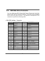
JUKI-730
Version 3.0
386SX with LCD/CRT
& 4COM SBC
User Manual
Version 3.1
August 11, 2003
© Copyright 2003 by ICP Electronics Inc. All Rights Reserved.
1
Copyright Notice
The information in this document is subject to change without
prior notice in order to improve reliability, design and function and
does not represent a commitment on the part of the manufacturer.
In no event will the manufacturer be liable for direct, indirect,
special, incidental, or consequential damages arising out of the
use or inability to use the product or documentation, even if advised of the possibility of such damages.
This document contains proprietary information protected by
copyright. All rights are reserved. No part of this manual may be
reproduced by any mechanical, electronic, or other means in any
form without prior written permission of the manufacturer.
Trademarks
JUKI-730 is registered trademarks of ICP Electronics Inc., PC/104
is trademarked of PC/104 Consortium, IBM PC is a registered
trademark of International Business Machines Corporation. Intel
is a registered trademark of Intel Corporation. AMI is registered
trademarks of American Megatrends, Inc. Other product names
mentioned herein are used for identification purposes only and
may be trademarks and/or registered trademarks of their
respective companies.
2
Table of Contents
1. INTRODUCTION ........................................................5
1.1
SPECIFICATIONS .....................................................6
1.2
PACKAGE CONTENTS.................................................8
2. INSTALLATION..........................................................9
2.1
JUKI-730'S LAYOUT ................................................9
2.2
CPU SETTING FOR JUKI-730 VER. 3.0........................ 11
2.3
SYSTEM MEMORY................................................... 11
2.4
WATCH-DOG T IMER ............................................... 12
2.5
DISK ONCHIP™
2.6
BIOS FLASH CHIP VPP SETTING ................................. 13
2.7
CLEAR CMOS SETUP.............................................. 13
2.8
COM3(CN17) RS232/422/485 SETTING .................... 14
2.9
COM3/COM4 RI PIN SETTING.................................. 15
F LASH DISK .................................... 13
3. CONNECTION .......................................................... 16
3.1
F LOPPY DISK DRIVE CONNECTOR................................. 16
3.2
IDE DISK DRIVE CONNECTOR .................................... 17
3
3.3
PARALLEL PORT..................................................... 18
3.4
SERIAL PORTS ...................................................... 19
3.5
IRDA INFRARED INTERFACE PORT................................ 20
3.6
KEYBOARD /MOUSE CONNECTOR .................................. 21
3.7
EXTERNAL SWITCHES AND INDICATORS .......................... 21
3.8
EXTERNAL POWER CONNECTOR ................................... 22
3.9
EXTERNAL SPEAKER................................................ 23
3.10
PC/104 CONNECTION BUS ....................................... 23
3.11
LCD INTERFACE CONNECTOR..................................... 23
4. AMI BIOS SETUP ..................................................... 25
4.1
GETTING START .................................................... 25
4.2
STANDARD CMOS SETUP......................................... 25
4.3
ADVANCED CMOS SETUP ......................................... 26
APPENDIX A. E2 KEY™ FUNCTION............................... 28
APPENDIX B. WATCH- DOG TIMER ................................ 30
APPENDIX C. PANEL SUPPORT LIST ........................... 31
APPENDIX D. HOW TO UPDATE THE BIOS..................... 32
4
1. Introduction
Thank you for choosing JUKI-730 386SX with LCD/CRT/4COM
Single Board Computer. The JUKI-730 is an ISA with PC/104 form
factor board, which comes equipped with ALI 6117 (386SX CPU
included) and an advanced high-performance multi- mode I/O,
designed for the system manufacturers, integrators, or VARs that
want to provide all the performance, reliability, and quality at a
reasonable price.
An advanced high performance super AT I/O chip Windbond
W83877F and SMC FDC37C669 are used in the JUKI-730 board.
Both on-chip UARTs are compatible with the NS16C550 and one
COM port can be set in RS232, RS422, or RS485. The parallel port
and IDE interface are compatible with IBM PC/AT and XT
architectures, as well as EPP and ECP.
The LCD/CRT controller is TOPRO TP-6508, which can provide
both LCD and CRT display at the same time. The LCD interface
connector is a 44-pin 2.0mm pitch type.
The most outstanding feature in the JUKI-730 is the built-in
PC/104 expansion bus. Based on the PC/104 bus, you could easily
install over thousands of PC/104 modules manufactured by
hundreds of vendors worldwide. Aside from that, the JUKI-730
has an external power connector that allows direct connection to
a power supply making it more suitable for your standalone
applications.
5
1.1
l
l
l
Specifications
System :
ü
CPU: ALI 6117,includes 386SX CPU
ü
DMA channels:
ü
Interrupt levels: 15
ü
Real-time clock/calendar:
DS12887/BQ3287 or
equivalent chip and quartz oscillator, 128B CMOS
memory, powered by lithium battery for over 10 years
of data retention.
7
Memory :
ü
RAM memory: 512KB to 32MB, only support single
side 16-bit SIMM.
ü
Shadow RAM Memory: C0000h ~ DFFFFh
ü
System BIOS: 0E0000h ~ 0FFFFFh
LCD/CRT Interface:
ü
Chipset: TP-6508
ü
Resolution: Support up to 800 x 600 resolution for STN
and TFT LCD Flat Panel. And Support 1024x768 256
colors for CRT display.
ü
Display Memory: 1MB on board.
6
l
Input/Output:
ü
IDE hard disk drive interface: Supports up to two
IDE hard disk drives. Can be disabled through BIOS
Setup Menu setting.
ü
Floppy disk drive interface: Supports two 2.88 MB,
1.44MB, 1.2MB, 720KB, or 360KB floppy disk drives.
Can be disabled through BIOS Setup Menu setting.
ü
Two high speed Series ports: NS16C550 compatible
UARTs with send/receive 16-byte FIFOs, data rates are
independently programmable from 115.2K baud down
to 50 baud. The modem controls the circuitry.
ü
Multi-mode Parallel Port:
Standard mode - IBM PC/XT, PC/AT, PS/2 compatible
bi-directional parallel port.
Enhanced mode - Enhanced parallel port (EPP)
compatible with IEEE 1284 specification.
High speed mode - Microsoft and Hewlett Packard
extended capabilities port (ECP), compatible with IEEE
1248 specification.
l
Industrial features :
ü
Watch-dog timer: Can be set to 1,2,10,20,110,or
220 seconds per period. Reset or NMI was generated
when CPU did not periodically trigger the timer. Your
program use hex 043 and 443 to control the watch-dog
and generate a system reset.
ü
PC/104 expansion bus: A 64-pin and 40-pin,
industrial embedded-PC bus standard.
ü
External power connector: 8-pin male connector
( Molex 6410 series compatible)
7
ü
l
1.2
Keyboard connector: A 5-pin header on board and
6-pin mini-DIN keyboard connector is located on the
mounting bracket.
General :
ü
Power Consumption: +5V @ 1.53A ( 40MHz,8MB
RAM)
ü
Operating Temperature: 0 ° ~ 55° C
ü
Humidity : 5% ~ 95%, non-condense
ü
Dimension: 180mm(W) x 122mm(L), standard AT
form factor.
Package Contents
In addition to this User's Manual, the JUKI-730 package
includes the following items:
•
One JUKI-730 386SX with LCD/CRT/4COM Single Board
Computer
•
One RS-232/Printer Cable & RS-232 x 2 Cable
•
One FDD/HDD Cable
8
2. Installation
This chapter describes how to install the JUKI-730. First, the
layout of JUKI-730 is shown, and then the unpacking
information that you should be careful with is described.
After that comes the setting for jumpers and switches for the
JUKI-730's configuration, with information such as CPU type
selection, system clock setting, and interrupt IRQ setting for
serial ports and parallel port and other such settings.
2.1 JUKI-730's Layout
<Please turn to the next page>
9
10
2.2
CPU Setting for JUKI-730 Ver. 3.0
• CPU SPEED SETTING:
The system clock is generated by the AV9155C-02, and
different CPU clock frequency can be selected through JP3
setting in the manner shown in the following table:
JP3
8MHz
16Mhz
20MHz
25MHz
40MHz
2.3
1-2
OPEN
CLOSE
OPEN
CLOSE
CLOSE
3-4
CLOSE
OPEN
OPEN
CLOSE
OPEN
5-6
CLOSE
CLOSE
CLOSE
OPEN
OPEN
System Memory
The system DRAM on board is divided into two banks, bank 0
and 1. Bank 0 is the on board optional 2/4MB DRAM. Bank 1 is
a 72-pin SIMM. Based on the chipset function the 72-pin SIMM
only supports single side DRAM. There are two jumpers
related to this setting.
• JP1/JP2 : 2/4MB DRAM and 72-pin SIMM selection
Function
On Board 2/4MB
72-pin SIMM
JP1
CLOSE
OPEN
11
JP2
CLOSE
OPEN
2.4
Watch-Dog T imer
The Watch-Dog Timer is enabled through reading port 443H.
It should be triggered before time -out period ends, otherwise
it will assume that program operation is abnormal and will
issue a reset signal to start again, or activate NMI to CPU. The
Watch-Dog Timer can be disabled through reading port 043H.
The Watch-Dog Timer time-out period can be set
1,2,10,20,110 or 220 sec. using jumper JP16.
• JP18 : Watch-Dog Active Type Setting
JP18
2-3
1-2
OPEN
DESCRIPTION
RESET WHEN WDT TIME-OUT
ACTIVATE NMI TO CPU WHEN WDT
TIME-OUT
DISABLE WDT
• JP16 : WDT TIME-OUT PERIOD
JP16
1sec
2sec
10sec
20sec
110sec
220sec
1-2
OPEN
OPEN
OPEN
OPEN
CLOSE
CLOSE
3-4
OPEN
OPEN
CLOSE
CLOSE
OPEN
OPEN
12
5-6
CLOSE
CLOSE
OPEN
OPEN
OPEN
OPEN
7-8
OPEN
CLOSE
OPEN
CLOSE
OPEN
CLOSE
2.5
DiskOnChip™
Flash Disk
The DiskOnChip™ Flash Disk Chip (DOC) is produced by
M-Systems. The DOC (MD-2200-xMB) is 32-pin DIP package.
As DOC is 100% compatible to hard disk and DOS, users don‘t
need to install any extra software utility. “Plug and play”
function is not only easy to use but also reliable. Currently,
DOC is available from 2MB to 72MB in capacity.
• JP19 : DiskOnChip™ Memory Address Setting
Address
CE000
D6000
DE000
1-2
CLOSE
OPEN
OPEN
3-4
OPEN
CLOSE
OPEN
5-6
OPEN
OPEN
CLOSE
2.6 BIOS Flash Chip Vpp Setting
There are two types of Flash chips that can be installed unto
this board, one is 5V Vpp and the other is 12V Vpp. The Vpp is
provided to undergo programming functions.
Function
5V Vpp
12V Vpp
JP24
2-3
1-2
2.7 Clear CMOS Setup
If you want to clear CMOS Setup (for example you forgot the
password then you should clear the setting and then reset the
password), you should close JP13 for about 3 seconds, then
reopen it. To set back to normal operation mode please take
13
off the jumper. If the RTC Chip is Dallas DS12B887 then you
should finish this procedure while the board is in power on
mode.
• JP13 : Clear CMOS Setup (Reserve Function)
JP13
OPEN
CLOSE
DESCRIPTION
Normal Operation
Clear CMOS Setup
2.8 COM3(CN17) RS232/422/485 Setting
COM3 can be set in RS232 or RS422/ RS485 interface using
Jumper JP20/JP23. If you select RS422/485 then you need to
reset JP21 for RS422 or RS485.
• JP23 : COM3 RS-232 or RS-422/485 setting
Description
RS-232
RS-422
or
RS-485
JP23
1-9
close
3-10
close
5-11
close
7-12
close
JP20
2-3
1-2
3-4
5-6
7-8
1-2
close
close
close
close
• JP21 : COM3 RS-422 or RS-485 setting
JP21
2-3
1-2
DESCRIPTION
RS-422
RS-485
14
2.9 COM3/COM4 RI Pin Setting
COM3 and COM4 can supply +5V or +12V power to the serial
devices via RI pin (Pin 9) of the COM port connector. The
maximum current provided is 1A with fuse protection for total
of two connectors’ 5V/12V outputs.
• JP9/JP29 : COM3(CN17),Pin 9
RI signal or 5V/12V output selection
Function
RI Signal
5V
12V
• JP8/JP10 :
JP9
2-3
1-2
1-2
JP29
1-2
1-2
2-3
COM4(CN14),Pin 9
RI signal or 5V/12V output selection
Function
RI Signal
5V
12V
JP8
2-3
1-2
1-2
15
JP10
1-2
1-2
2-3
3. Connection
This chapter describes how to connect peripherals, switches and
indicators to the JUKI-730 board. You can access most of the
connectors from the top of the board while it is installed inside the
chassis.
3.1
Floppy Disk Drive Connector
JUKI-730 board comes equipped with a 34-pin daisy-chain driver
connector cable. The detailed pin assignment of the connector is
specified as following table:
• CN5 : FDC CONNECTOR
PIN NO.
DESCRIPTION PIN NO. DESCRIPTION
1
GROUND
2
REDUCE WRITE
CURRENT#
3
GROUND
4
N/C
5
GROUND
6
N/C
7
GROUND
8
INDEX#
9
GROUND
10
MOTOR ENABLE A#
11
GROUND
12
DRIVE SELECT B#
13
GROUND
14
DRIVE SELECT A#
15
GROUND
16
MOTOR ENABLE B#
17
GROUND
18
DIRECTION#
19
GROUND
20
STEP#
21
GROUND
22
WRITE DATA#
23
GROUND
24
WRITE GATE#
25
GROUND
26
TRACK 0#
27
GROUND
28
WRITE PROTECT#
29
GROUND
30
READ DATA#
31
GROUND
32
SIDE 1 SELECT#
33
GROUND
34
DISK CHANGE#
16
3.2
IDE Disk Drive Connector
You can attach two IDE (Integrated Device Electronics) hard disk
drives to the JUKI-730 internal controller. The board comes equipped
with a 40-pin flat -cable connector. The detailed pin assignment of the
connector is specified as following table:
• CN4: IDE Interface Connector
PIN NO.
DESCRIPTION
PIN NO.
DESCRIPTION
1
RESET#
2
GROUND
3
DATA 7
4
DATA 8
5
DATA 6
6
DATA 9
7
DATA 5
8
DATA 10
9
DATA 4
10
DATA 11
11
DATA 3
12
DATA 12
13
DATA 2
14
DATA 13
15
DATA 1
16
DATA 14
17
DATA 0
18
DATA 15
19
GROUND
20
N/C
21
N/C
22
GROUND
23
IOW#
24
GROUND
25
IOR#
26
GROUND
27
N/C
28
BALE - DEFAULT
29
N/C
30
GROUND - DEFAULT
31
INTERRUPT
32
IOCS16#-DEFAULT
33
SA1
34
N/C
35
SA0
36
SA2
37
HDC CS0#
38
HDC CS1#
39
HDD ACTIVE#
40
GROUND
17
3.3
Parallel Port
This port is usually connected to a printer. The JUKI-730
includes an on-board parallel port, which is accessed through
a 26-pin flat-cable connector CN12. The detailed pin
assignment of the connector is specified in the following table:
• CN12 : Parallel Port Connector
PIN NO.
DESCRIPTION
PIN NO.
DESCRIPTION
1
STROBE#
2
DATA 0
3
DATA 1
4
DATA 2
5
DATA 3
6
DATA 4
7
DATA 5
8
DATA 6
9
DATA 7
10
ACKNOWLEDGE
11
BUSY
12
PAPER EMPTY
13
PRINTER SELECT
14
AUTO FORM FEED #
15
ERROR#
16
INITIALIZE
17
PRINTER SELECT LN#
18
GROUND
19
GROUND
20
GROUND
21
GROUND
22
GROUND
23
IOW#
24
GROUND
25
GROUND
18
3.4
Serial Ports
The JUKI-730 offers two high speed NS16C550 compatible
UARTs with Read/Receive 16 byte FIFO serial ports. These
ports let you connect to serial devices or a communication
network. One DB-9 connector and thee 10-pin headers are
provides by the JUKI-730. The detailed pin assignment of the
connectors are specified as following tables:
• COM1(CN1) : Serial Port Connector
PIN NO.
1
DESCRIPTION
DATA CARRIER DETECT
(DCD)
2
RECEIVE DATA
(RXD)
3
TRANSMIT DATA
(TXD)
4
DATA TERMINAL READY
(DTR)
5
6
GROUND
DATA SET READY
(GND)
(DSR)
7
REQUEST TO SEND
(RTS)
8
CLEAR TO SEND
(CTS)
9
RING INDICATOR
(RI)
• COM2(CN21) : 2x5-pin Header at RS-232 mode
PIN NO.
DESCRIPTION
PIN NO.
DESCRIPTION
1
DCD
6
DSR
2
RXD
7
RTS
3
TXD
8
CTS
4
DTR
9
RI
5
GND
10
N/C
19
• COM3(CN17) : 2x5-pin Header at
RS-422/485 mode
PIN NO.
DESCRIPTION
PIN NO.
DESCRIPTION
1
TX-
6
RX+
2
TX+
7
RX-
3
8
4
9
5
10
• COM3 (CN17) and COM4(CN14) : 2x5-pin Header
PIN NO.
3.5
DESCRIPTION
PIN NO.
DESCRIPTION
1
DCD
6
DSR
2
RXD
7
RTS
3
TXD
8
CTS
4
DTR
9
RI or 5V/12V
5
GND
10
N/C
IrDA Infrared Interface Port
The JUKI-730 built-in IrDA port which support Serial Infrared
(IR) or Amplitude Shift Keyed IR(ASKIR) interface. When you
need to use the IrDA port, you will have to configure SIR or
ASKIR model in the BIOS’s COM2 setup. Then the normal
RS-232 COM2 will be disabled.
• CN6 : IrDA Connector
PIN NO.
DESCRIPTION
1
5V
2
N/C
3
IR-RX
4
GND
5
IR-TX
20
3.6 Keyboard/Mouse Connector
The JUKI-730 provides two keyboard connectors. A 5-pin header
connector CN18 supports passive backplane applications. Another
one is a 6-pin Mini-DIN connector CN19 on the board mounting
bracket for single board computer applications.
• CN18 : 5-pin Header Keyboard Connector
PIN NO.
DESCRIPTION
1
KEYBOARD CLOCK
2
KEYBOARD DATA
3
N/C
4
GROUND
5
+5V
• CN19/16 : 6-pin Mini- DIN Keyboard/Mouse Connector
PIN NO.
DESCRIPTION
1
KEYBOARD DATA
2
N/C
3
GROUND
4
+5V
5
KEYBOARD CLOCK
6
N/C
MOUSE DATA
N/C
GROUND
+5V
MOUSE CLOCK
N/C
3.7 External Switches and Indicators
There are many external switches and indicators for monitoring and
controlling your CPU board. These features are completely optional
so please install them if you need them.
The detailed pin
assignment of the connectors is specified in the following table:
21
• CN7 : RESET BUTTON
PIN NO.
DESCRIPTION
1
EXTERNAL RESET
2
GROUND
• CN11 : IDE LED connector
PIN-NO
DESCRIPTION
1
+5V
2
HDD ACTIVE#
• CN8 : POWER LED & KEYLOCK
PIN NO.
3.8
DESCRIPTION
1
POWER LED ANODE
2
KEY
3
GROUND
4
KEYLOCK
5
GROUND
External Power Connector
The JUKI-730 has an on-board external power connector CN13. You
can connect power directly to the CPU board for some
single-board-computer (without passive backplane) application.
• CN13 : EXTERNAL POWER CONNECTOR
PIN NO.
DESCRIPTION
1
+5V
2
+12V
3
-12V
4
GROUND
5
GROUND
22
6
-5V
7
+12V
8
+5V
3.9 External Speaker
The JUKI-730 has its own buzzer, you can also connect an external
speaker through the connector CN3.:
• CN3 : SPEAKER
PIN NO.
DESCRIPTION
1
GROUND
2
SPEAKER SIGNAL
3.10 PC/104 Connection Bus
The JUKI-730's PC/104 expansion bus allows you to attach any kind
of PC/104 modules onto it. The PC/104 bus has already become the
industrial embedded PC bus standard, so you could easily install over
thousands of PC/104 modules coming from hundreds of venders
worldwide.
NOTE:
JUKI-730 allows direct plug in of PC/104
modules so don‘t need to use the PC/104
Connection Kit.
3.11 LCD Interface Connector
The JUKI-730 provides a 2x22-pin connector suitable for LCD flat
panel interfaces.
23
• CN20: LCD Interface Connector
PIN NO.
DESCRIPTION
PIN NO.
DESCRIPTION
1
+12V
2
+12V
3
GND
4
GND
5
+5V
6
+5V
7
FPVEE
8
GND
9
P0
10
P1
11
P2
12
P3
13
P4
14
P5
15
P6
16
P7
17
P8
18
P9
19
P10
20
P11
21
P12
22
P13
23
P14
24
P15
25
P16
26
P17
27
P18
28
P19
29
P20
30
P21
31
P22
32
P23
33
GND
34
GND
35
SHFCLK
36
FLM
37
M
38
LP
39
GND
40
ENABLK
41
GND
42
N/C
43
FPVDD
44
5V
24
4. AMI BIOS Setup
The JUKI-730 use AMI BIOS for system configuration, and the AMI
BIOS setup program is designed to provide maximum flexibility in
configuring the system by offering various options which may be
selected to fit end-users’ individual demands. This chapter is written
to demonstrate how you can use these features properly.
4.1 Getting Start
When the system is powered on, the BIOS will enter the
Power-On-Self-Test routines. These routines will be executed for
System Test, Initialization and System Configuration Verification. After
the POST routines are completed, the following message appears:
" Hit < Del>, if you want to run SETUP"
To access AMI BIOS Setup program, press <Del> key.
4.2 Standard CMOS Setup
Standard CMOS Setup is the first option on the main menu.
The standard CMOS setup utility is used to configure the following
features:
•Date/Time
•Hard Disk Type
•Floppy Disk Type
All of these features are very commonly seen so we here do not
describe in detail.
25
4.3 Advanced CMOS Setup
After you enter the Advanced CMOS Setup you will see that this
Setup program is equipped with a series of help screens, accessed
through pressing <F1> key, which will display the options available for
a particular configuration features.
All the items on the left side of the screen are very common so they
will not be mentioned within this manual. Here, we will focus on some
special items that are only found in JUKI-730. These items are
specified below:
•On-board IDE Controller : The IDE hard disk drive can be
Enable or Disable through this item. When
you do not need the hard disk, the IDE
controller can be disabled.
•On-board Floppy Controller : The floppy disk drive can be
Enable or Disable through this item. When
you do not need floppy disk, the FDD
controller can be disabled.
•Serial Port 1 : The options are Disable, 3E8,2F8 , or 3F8.
You can either set the I/O address of the
serial port (COMA) or disable it.
•Serial Port 2 : The options are Disable, 2E8,3F8,or 2F8.
You can either set the I/O address of the
serial port 1 (COMB) or disable it.
•Parallel Port : The options are Disable, 3BC, 378 or 278.
You can either set the I/O address of the
parallel port or disable it.
•Parallel Port Mode : JUKI-730 provides
EPP,ECP,ECP+EPP, and Normal Mode.
•Primary Display : You could set VGA/EGA, CGA40x25,
CGA80x25, Mono or Absent. When
configured to Absent, JUKI-730 will not
check the display adapter while powering on
the system.
26
•System Keyboard : You could set Present or Absent.
When set Absent, JUKI-730 board will not
check the display adapter while powering on
the system.
27
Appendix A. E2 Key™ Function
The JUKI-730 provides an outstanding E2KEY™ function for
system integrator. Based on the E2KEY™ you could free to store
the ID Code, Pass Word, or Critical Data in the 1Kbit EEPROM.
Because the EEPROM is a nonvolatile memory, you don’t have to
worry about losing very important data.
2
Basically the E KEY™ is based on a 1Kbit EEPROM, which is
configured to 64 words (from 0 to 63). You could access (read or
write) each word anytime.
2
When you need to use E KEY™ please find the utility enclosed in
the package. The software utility will include the following four
files
README.DOC
E2KEY.OBJ
EKEYDEMO.C
EKEYDEMO.EXE.
E2KEY.OBJ provides two library function for user to integrate their
2
application using E KEY™ function. These libraries (read_e2key
and write_e2key) are written and compiled in C format. For
easy implementation, please refer to the following statements.
unsigned int read_e2key(unsigned int address)
2
/* This function will return the E KEY™ ’s data at address. The address range is
from 0 to 63. Return data is one word, 16 bits */
void write_e2key(unsigned int address,unsigned data)
2
/* This function will write the given data to E KEY™ at address. The address range
is from 0 to 63. The data value is from 0 to 0xffff. */
For easy start, please refer to the included EKEYDEMO.C code first.
28
Please note the E2KEY™ function is based on the working of
parallel port. So you should enable the JUKI-730’s parallel port,
otherwise will not be working.
29
Appendix B. Watch-Dog Timer
The Watch-Dog Timer is provided to ensure that standalone
systems can always recover from catastrophic conditions that
caused the CPU to crash. This condition may have occurred by
external EMI or a software bug. When the CPU stops working
correctly, hardware on the board will either perform a hardware
reset (cold boot) or a non- maskable interrupt (NMI) to bring the
system back to a known state.
The Watch-Dog Timer is controlled by two I/O ports.
443
(hex)
043
(hex)
Read
Read
Enable the refresh the Watch-Dog
Timer.
Disable the Watch-Dog Timer.
To enable the Watch-Dog Timer, a read from I/O port 443H must
be performed. This will enable and activate the countdown timer,
which will eventually time out, and either a reset action of the
CPU or cause an NMI will occur depending on the setting of JP18.
To ensure that this reset condition does not occur, the Watch-Dog
Timer must be periodically refreshed by reading the same I/O
port 433H. This must be done within the time out period that is
selected by jumper JP16.
A tolerance of at least 30% must be maintained to avoid unknown
routines within the operating system (DOS), such as disk I/O that
can be very time consuming. Therefore if the time out period has
been set to 10 seconds, the I/O port 443H must be read within 7
seconds.
Note: When exiting a program, it is necessary to disable the
Watch-Dog Timer, otherwise the system will reset.
30
Appendix C. Panel Support List
JUKI-730 supports a wide range flat panels. Different flat panels
will need different LCD drive set in the BIOS Setup Menu. The
default setting is for Color DSTN flat panel. The available BIOS for
different panels are listed below. Please note that all BIOS files
already include system BIOS and LCD drive BIOS, so you only
need to re-program the BIOS flash chip with the file then power
on again.
MLCD.ROM – BIOS for MONO DSTN 640x480
For example : HOSIDEN HLM6667
HITACHI LMG5160XUFC
CASIO MD650TS00-01
OPTREX DMF_50260NFU-FW-8
DSTN.ROM – BIOS for Color DSTN 640x480
For example : SANYO LCM-5331-22NTK
SHARP LM64C35P
TFT_S1.ROM – BIOS for TFT 640x480-SYNC (16-bit)
TFT_S2.ROM – BIOS for TFT 640x480-SYNC (18/24-bit)
For example : HITACHI TX26D60/TX24D55
TOSHIBA LTM09C015A
SHARP LQ10D321
TFT_LP1.ROM – BIOS for TFT 640x480-LP(16-bit)
TFT_LP2.ROM – BIOS for TFT 640x480-LP(16/24-bit)
For example : TOSHIBA LTM09C015A
TFT86_S1.ROM – BIOS for TFT 800x600-SYNC(16-bit)
TFT86_S2.ROM – BIOS for TFT 800x600-SYNC(18/24-bit)
For example : NEC NL8060AC26-05
NEC NL8060AC26-04
NEC NL8060BC31-02
EL.ROM – BIOS for EL 640x480
For example : PLANAR EL640.480-A
PLASMA.ROM – BIOS for PLASMA 640x480
For example : PANASONIC S817
31
Appendix D. How to Update the BIOS
1. You can use EPROM Programmer setting to configure the
right type of Flash then write the file into the Flash. To apply
this method, you should carefully take Flash chip out of
socket and then put it back after you finish programming.
Most commonly seen flash type is: ATMEL AT29C010A
Or,
2. There is also a utility (FLASH634.COM) that can be used to
re-program the BIOS directly under DOS environment.
For example:
C:>FLASH634 MLCD.ROM
32