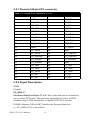
1
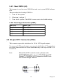
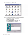
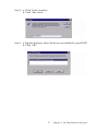
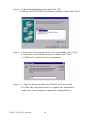
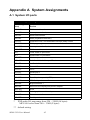
SOM-2354
Geode™ GX533 SOM 144
System On Module
User Manual
Copyright notice
This document is copyrighted, 2001, by Advantech Co., Ltd. All rights
are reserved. The original manufacturer reserves the right to make
improvements to the products described in this manual at any time
without notice.
No part of this manual may be reproduced, copied, translated or transmitted in any form or by any means without the prior written permission of
the original manufacturer. Information provided in this manual is
intended to be accurate and reliable. However, the original manufacturer
assumes no responsibility for its use, nor for any infringements upon the
rights of third parties which may result from its use.
Acknowledgements
SOM and DTOS are trademarks of Advantech Co., Ltd. AMD is a
trademark of Advanced Micro Devices, Inc.
Award is a trademark of Award Software International, Inc.
Cyrix is a trademark of Cyrix Corporation.
IBM, PC/AT, PS/2 and VGA are trademarks of International Business
Machines Corporation.
Intel and Pentium are trademarks of Intel Corporation.
Microsoft Windows® is a registered trademark of Microsoft Corp.
RTL is a trademark of Realtek Semiconductor Co., Ltd.
C&T is a trademark of Chips and Technologies, Inc.
UMC is a trademark of United Microelectronics Corporation.
Winbond is a trademark of Winbond Electronics Corp.
STPC is a trademark of SGS Thomson Corp.
For more information on this and other Advantech products, please visit
our website at: http://www.advantech.com
For technical support and service, please visit our support website at:
http://www.advantech.com/support
This manual is for SOM-2354
Part No. 2006235400
1st Edition, Printed in Taiwan Dec. 2004
SOM-2354 User Manual
ii
Packing list
Before you begin installing your card, please make sure that the following
materials have been shipped:
• 1 SOM-2354 System On Module CPU module
• CD-ROM or Disks for utility, drivers, and manual (in PDF format)
If any of these items are missing or damaged, contact your distributor or
sales representative immediately.
iii
This device complies with the requirements in part 15 of the
FCC rules: Operation is subject to the following two
conditions:
FCC 1.This device may not cause harmful interference, and
2. This device must accept any interference received,
including
interference that may cause undesired operation
This equipment has been tested and found to comply with
the limits for a Class A digital device, pursuant to Part 15 of
the FCC Rules. These limits are designed to provide
reasonable protection against harmful interference when
the equipment is operated in a commercial environment.
This equipment generates, uses, and can radiate radio
frequency energy and, if not installed and used in
accordance with the instruction manual, may cause
harmful interference to radio communications. Operation of
this device in a residential area is likely to cause harmful
interference in which case the user will be required to
correct the interference at his/her own expense. The user
is advised that any equipment changes or modifications not
expressly approved by the party responsible for
compliance would void the compliance to FCC regulations
and therefore, the user’s authority to operate the
equipment.
Caution!
There is a danger of a new battery exploding if it is
incorrectly installed. Do not attempt to recharge, force
open, or heat the battery. Replace the battery only with the
same or equivalent type recommended by the
manufacturer. Discard used batteries according to the
manufacturer’s instructions.
SOM-2354 User Manual
iv
Contents
Chapter
1 General Information ....................................... 2
1.1 Introduction ................................................................................. 2
1.2 Specifications............................................................................... 3
1.2.1 Mechanical and Environmental ................................................ 4
1.3 Board layout: dimensions ............................................................ 5
Chapter
2 Installation ....................................................... 8
2.1 Jumpers and connectors............................................................... 8
Table 2.1: Jumpers and connectors ......................................... 8
2.2 Board layout: jumper/connector locations................................... 9
Figure 2.1:
Figure 2.2:
Board layout: jumper/connector locations .......... 9
Solder side connectors ...................................... 10
2.3 Safety precautions...................................................................... 11
2.4 Setting jumpers .......................................................................... 12
2.4.1 Clear CMOS (J2) .................................................................... 13
2.4.2 Panel Type Selection (SW1) .................................................. 13
2.5 40-pin FPC Connector (CN1).................................................... 13
2.5.1 Pinout of 40-pin FPC connector ............................................. 14
Table 2.2: 40-pin FPC connector (CN1) ............................... 14
2.5.2 Signal Description .................................................................. 14
2.6 CompactFlash interface (CN2).................................................. 16
2.7 144-pin SODIMM of SOM 144/PCI (PCI/IDE/ Serial port /USB/
AC97/KB/Mouse)(CN3) ........................................................... 16
2.8 Recommended front-end 80-pin connector (VGA/Ethernet/IrDA/
Printer/FDD/ATX) (CN4) ......................................................... 16
2.9 Card installation......................................................................... 17
2.10 Card removal ............................................................................. 18
v
Table of Contents
Chapter
3 Software Configuration ................................ 20
3.1 Introduction ............................................................................... 20
3.2 Utility CD disk........................................................................... 20
Figure 3.1:
Contents of the SOM-2354 utility disk ............. 20
3.3 VGA display software configuration......................................... 21
Figure 3.2:
BIOS VGA setup screen ................................... 21
3.4 Ethernet interface configuration ................................................ 23
Chapter
4 PCI Graphic Setup........................................ 26
4.1 Introduction ............................................................................... 26
4.1.1 Chipset .................................................................................... 26
4.1.2 Display memory ..................................................................... 26
4.1.3 Display types .......................................................................... 26
4.2 Installation of the PCI Graphic driver ....................................... 27
4.2.1 Installation for Windows 98/ME/2000/XP ............................. 27
4.3 Further Information ................................................................... 30
Appendix A System Assignments ...................................... 42
A.1 System I/O ports ........................................................................ 42
Table A.1: System I/O ports .................................................. 42
A.2 DMA channel assignments........................................................ 43
Table A.2: DMA channel assignments .................................. 43
A.3 Interrupt assignments................................................................. 44
Table A.3: Interrupt assignments ........................................... 44
A.4 1st MB memory map ................................................................. 45
Table A.4: 1st MB memory map ........................................... 45
Appendix B LCD Services ................................................. 48
B.1 LCD services ............................................................................. 48
SOM-2354 User Manual
vi
CHAPTER
1
2
General Information
This chapter provides background
information for the SOM-2354.
Sections include:
• Card specifications
• Board layout
Chapter 1 General Information
1.1 Introduction
Advantech's new SOM 144 Module, the SOM-2354, a Geode GX1
system on module comes equipped with 64M SDRAM , a VGA interface
which supports CRT monitor with up to 4MB display memory, two USB
interfaces, IrDA interfaces, AC 97 interfaces, a 10/100 base-T Ethernet
interface (for SOM-2354) and a Compact Flash solid state disk socket
(for SOM-2354). In addition, it is equipped with two RS-232 serial ports.
One bi-directional printer port supports SPP, ECP and EPP modes. Three
master PCI interfaces, an IDE HDD interface and a floppy disk controller
provide functional expansion. With its industrial grade reliability, the
SOM-2354 can operate continuously at temperatures up to 140° F
(60° C). This compact unit offers all these functions within the space of a
2.5" hard disk drive (68mm * 100mm). The numerous features provide an
ideal price/performance solution for high-end commercial and industrial
applications where stability and reliability are essential. The SOM-2354
is compact; highly integrated; and easy to maintain, upgrade, and install.
These features make it ideal for applications of small industrial controller,
Panel PC, security system, Internet gateway, instruments, medical
equipment, building automation and so on.
SOM-2354 User Manual
2
1.2 Specifications
CPU: On-board AMD TM Geode TM GX533-400 MHz processor
Chipset: AMD CS 5535
BIOS: Insyde 256KB FLASH BIOS
RAM memory: 128 MB DDR DRAM on board.
SSD: CompactFlash socket
PCI/IDE/ Serial port /USB/AC97/KB/Mouse (SODIMM socket ):
I/O expansion: 3 master PCI bus (3.3V PCI)
Enhanced IDE hard disk drive interface:
Supports up to two hard disk drives. BIOS auto-detect. (DMA33)
Serial ports: Support two serial ports ,TTL signal
PS/2 Keyboard and PS/2 Mouse
Universal Serial Bus:
Two independent USB interfaces (OpenHCI, Rev. 1.0) specification
compliant
AC97 codec interface:
AC97 Specification Revision 1.3, 2.0, and 2.1 compliant interface.
VGA/Ethernet/IrDA/FDD/Printer/ATX Power (front-end connector):
VGA:
2D Graphics Accelerator, supports VGA and VESA
Display memory: up to 16 MB share memory
Supports up to 1024x268 @ 24 bpp (60 Hz)
10/100 Base T Ethernet interface: controller Intel 82551ER (SOM 2354
only)
Infrared: Supports IrDA version 1.0 SIR (115.2kbps)
Supports ATX power supply
Floppy disk drive interface/Multi-mode parallel port:
FDD interface and parallel port share the same bus either FDD or Parallel
port can be used at one time.
FDD interface supports up to two floppy disk drives
Parallel supports SPP, ECP and EPP.
3
Chapter 1
Power management: Supports power saving modes including Normal/
Doze/Sleep modes. APM 1.1 compliant
40 Pin FPC connector: 24 bit LCD signal output
Note:
All interfaces are compliant with SOM 144 Specification and Design Guide Rev 1.0
1.2.1 Mechanical and Environmental
Power supply voltage: +5 V± 5%
Power requirements: Max. : 5 V @ 1.4 A
Typical: 5 V @ 1A
Operating temperature: 32 to 140° F (0 to 60° C), fanless operation
Board Size: 68 mm x 100 mm
Weight: 0.07 Kg
SOM-2354 User Manual
4
1.3 Board layout: dimensions
2.00
5.85
5.85
2.00
SW1
CN1
101.85
76.00
76.00
SOM-2354
29.01
38.60
5
3.24
J1
CN2A
Chapter 1
SOM-2354 User Manual
6
CHAPTER
2
2
Installation
This chapter explains the setup
procedures of SOM-2354 hardware,
including instructions on setting
jumpers and connecting peripherals,
switches and indicators. Be sure to read
all safety precautions before you begin
the installation procedure.
Chapter 2 Installation
2.1 Jumpers and connectors
On-board connectors link to external devices such as hard disk drives,
keyboards, floppy drives, and so on. In addition, the board has jumpers
for configuring your board for specific applications.
The table below lists the function of each of the board’s jumpers and
connectors. Later sections in this chapter give detailed information on
each jumper setting, and instructions for connecting external devices to
your card.
Table 2.1: Jumpers and connectors
Name
Function
CN1
30 Pin FPC connector for 18-bit LCD signal
CN2 A
SODIMM gold finger (PCI/IDE/ Serial port /USB/AC97/KB/Mouse )
CN2 B
Front-end connector (VGA/Ethernet/IrDA/FDD/Printer)
JP1
Clear CMOS
SW 1
Panel type selection
SOM-2354 User Manual
8
2.2 Board layout: jumper/connector locations
SW1
CN1
SOM-2354
CN2A
J1
Figure 2.1: Board layout: jumper/connector locations
9
Chapter 2
CN2B
SOM-2354
Figure 2.2: Solder side connectors
SOM-2354 User Manual
10
2.3 Safety precautions
Warning!
Always completely disconnect the power cord
from your chassis whenever you are working on
it. Do not make connections while the power is
on because sensitive electronic components can
be damaged by the sudden rush of power. Only
experienced electronics personnel should open
the PC chassis.
Caution!
Always ground yourself to remove any static
charge before touching the CPU card. Modern
electronic devices are very sensitive to static
electric charges. Use a grounding wrist strap at
all times. Place all electronic components on a
static-dissipative surface or in a static-shielded
bag when they are not in the chassis.
11
Chapter 2
2.4 Setting jumpers
You may configure your card to match the needs of your application by
setting jumpers. A jumper is a metal bridge used to close an electric circuit. It consists of two metal pins and a small metal clip (often protected
by a plastic cover) that slides over the pins to connect them. To "close" a
jumper, you connect the pins with the clip. To "open” a jumper, you
remove the clip. Sometimes a jumper will have three pins, labeled 1, 2
and 3. In this case you would connect either pins 1 and 2, or 2 and 3.
1
Open
Closed
2
3
Closed 2-3
The jumper settings are schematically depicted in this manual as follows:
1 2 3
Open
Closed
Closed 2-3
A pair of needle-nose pliers may be helpful when working with jumpers.
If you have any doubts about the best hardware configuration for your
application, contact your local distributor or sales representative before
you make any changes.
Generally, you simply need a standard cable to make most connections.
SOM-2354 User Manual
12
2.4.1 Clear CMOS (J2)
This jumper is used to erase CMOS data and reset system BIOS information.
The procedure for clearing CMOS is:
1.
Turn off the system.
2.
Short pin 1 and pin 2.
3.
Turn on the system. The BIOS is now reset to its default setting.
2.4.2 Panel Type Selection (SW1)
SW1(3,4)
Panel Type
(1,1)
640 x 480 18bit
(1,0)
800 x 600 18bit
(0,1)
1024 x 768 18bit
(0,0)
Reserved
2.5 40-pin FPC Connector (CN1)
This connector provides interfaces for 18-bit LCD signal outputs.
To connect a LCD panel output, users need to build their LCD control cirket in the solution board or carrier board that they want to put SOM-2354
module on.
Note
About the LCD control circuit, please refer
SOM-DB2300.pdf or in your CD-ROM and NS
Geode™ CS5530A I/O Companion Multi-Function South Bridge Manual
13
Chapter 2
2.5.1 Pinout of 40-pin FPC connector
Table 2.2: 40-pin FPC connector (CN1)
Pin
Signal
Pin
Signal
1
GND
2
FP_DD2
3
FP_DD3
4
FP_DD4
5
FP_DD5
6
FP_DD6
7
FP_DD7
8
FP_DD8
9
FP_DD11
10
GND
11
FP_DD12
12
FP_DD13
13
FP_DD14
14
FP_DD15
15
FP_DD18
16
FP_DD19
17
FP_DD20
18
FP_DD21
19
GND
20
FP_DD22
21
FP_DD23
22
GND
23
FP_SCLK
24
FP_FVSYNC
25
FP_ENDISP
26
FP_FHSYNC
27
FP_EN_BL
28
FP_BIASEN
29
FP_VDDEN
30
GND
31
FP_DD0
32
FP_DD1
33
FP_DD8
34
FP_DD9
35
FP_DD16
36
FP_DD17
37
FP_NC
38
FP_NC
39
FP_NC
40
FP_NC
2.5.2 Signal Description
GND
Ground
FP_DD0~17
Flat Panel Data Port Lines 17 to 0. This is the data port to an attached
active matrix TFT panel. This port may optionally be tied to a DSTN
formatter chip, LVDS transmitter, or digital NTSC/PAL encoder.
F4BAR+Memory Offset 04h[7] enables the flat panel data bus:
0 = FP_DATA[17:0] is forced low
SOM-2354 User Manual
14
1 = FP_DATA[17:0] is driven based upon power sequence control
FP_SCLK
Flat Panel Clock.This is the clock for the flat panel interface.
FP_FVSYNC
Flat Panel Vertical Sync Output. This is the vertical sync for an
attached active matrix TFT flat panel. This represents a delayed version
of the input flat panel vertical sync signal with the appropriate pipeline
delay relative to the pixel data.
FP_FHSYNC
Flat Panel Horizontal Sync Output. This is the horizontal sync for an
attached active matrix TFT flat panel. This represents a delayed version
of the input flat panel horizontal sync signal with the appropriate pipeline
delay relative to the pixel data.
FP_EN
Flat Panel Display Enable Output. This is the display enable for an
attached active matrix TFT flat panel. This.signal qualifies active pixel
data on the flat panel interface.
FP_ENDISP
Display Enable Input. This signal qualifies active data on the pixel input
port. It is used to qualify active pixel data for all display modes and configurations and is not specific
FP_BIASEN
Flat Panel Backlight Enable Output. This is the enable signal for the
backlight power supply to an attached flat panel. It is under control of the
power sequence control logic.
FP_VDDEN
Flat Panel VDD Enable. This is the enable signal for the VDD supply to
an attached flat panel. It is under the control of power sequence control
logic. A transition on bit 6 of the Display Configuration Register
(F4BAR+Memory Offset 04h) initiates a power-up/down sequence.
15
Chapter 2
2.6 CompactFlash interface (CN2)
This socket accepts an IDE-compatible CompactFlash memory card.
The CompactFlash interface uses a secondary IDE channel, which should
be set as the master channel.
2.7 144-pin SODIMM of SOM 144/PCI (PCI/IDE/ Serial
port /USB/AC97/KB/Mouse)(CN3)
The SOM-2354 is compliant with SOM 144 Design Specification Rev.
1.0. For the description of each signal, please refer this document. You
may find it in the CD-ROM that comes with your SOM-2354 module.
2.8 Recommended front-end 80-pin connector (VGA/
Ethernet/IrDA/Printer/FDD/ATX) (CN4)
The SOM-2354 is compliant with the SOM 144 Design Specification
Rev. 1.0. For the description of each signal, please refer to this document.
It is included on the CD-ROM that comes with your SOM-2354 module.
SOM-2354 User Manual
16
2.9 Card installation
1.
Plug SOM 144 module into the solution board's SODIMM socket.
2.
Connect the front-end connector to the solution board
3.
Must screw the SOM 144 module and the solution board together.
17
Chapter 2
2.10 Card removal
1.
Unscrew two screws.
2.
Bend out the positioning holders of SODIMM socket and release the
SOM 144 module.
3.
Unplug SOM 144 module from the socket.
SOM-2354 User Manual
18
CHAPTER
3
2
Software Configuration
This chapter details the software configuration information. It shows you
how to configure the card to match
your application requirements.
Sections include:
• VGA display software configuration
• Ethernet interface configuration
Chapter 3 Software Configuration
3.1 Introduction
The SOM-2354 system BIOS and custom drivers are located in a 256 KB,
32-pin Flash ROM device, designated U14. A single Flash chip holds the
system BIOS and VGA BIOS. The display type can be configured via
software. This method minimizes the number of chips and eases configuration. You can change the display BIOS simply by reprogramming the
Flash chip.
3.2 Utility CD disk
The SOM-2354 is supplied with a software utility on CD-ROM. This disk
contains the necessary file for setting up the VGA display. Directories
and files on the disk are as follows:
AWDFLASH.EXE
CBROM.EXE
RSET8139.EXE
2354Vxxx.BIN
Figure 3.1: Contents of the SOM-2354 utility disk
AWDFLASH.EXE
This program allows you to update the BIOS Flash ROM.
2354V110.BIN
This binary file contains the system BIOS.
CBROM.EXE
This program allows you to combine your own VGA BIOS with system
BIOS (2354V110.BIN).
RSET8139.EXE
This program enables you to view the current Ethernet configuration,
reconfigure the Ethernet interface (medium type, etc.), and execute useful
diagnostic functions.
SOM-2354 User Manual
20
3.3 VGA display software configuration
The SOM-2354 on-board VGA/LCD interface supports an 18-bit TFT
LCD, flat panel displays and traditional analog CRT monitors. The
interface can drive CRT displays with resolutions up to 1024 x 768 in 16
bpp. It is also capable of driving color panel displays with resolutions of
1024 x 768 at 18 bpp. The LCD type is configured completely via the
software utility, so you do not have to set any jumpers. Configure the
LCD type as follows:
1.
Apply power to the SOM-2354 with a color TFT display attached.
This is the default setting for the SOM-2354. Make sure that the
AWDFLASH.EXE and *.BIN files are located in the working drive.
Note:
2.
Make sure that you do not run AWDFLASH.EXE
while your system is operating in EMM386 mode.
At the prompt, type AWDFLASH.EXE and press <Enter>. The
VGA configuration program will then display the following:
Figure 3.2: BIOS VGA setup screen
3.
At the prompt, type in the BIN file which supports your display.
When you are sure that you have entered the file name correctly
press <Enter>. The screen will ask “Do you want to save?” If you
wish to continue press Y. If you change your mind or have made a
mistake press N.
21
Chapter 3
4.
If you decide to continue, the screen will issue a prompt which will
then ask “Are you sure to program (Y/N)?” If you wish to continue,
press Y. Press N to exit the program.
The new VGA configuration will then write to the ROM BIOS chip. This
configuration will remain the same until you run the AWDFLASH.EXE
program and change the settings.
SOM-2354 User Manual
22
3.4 Ethernet interface configuration
The SOM-2354 on-board Ethernet interface supports all major network
operating systems. To configure the medium type, to view the current
configuration, or to run diagnostics, do the following:
1.
Power the SOM-2354 on. Make sure that the RSET8139.EXE file is
located in the working drive.
2.
At the prompt, type RSET8139.EXE and press <Enter>. The Ethernet configuration program will then be displayed.
3.
This simple screen shows all the available options for the Ethernet
interface. Just highlight the option you wish to change by using the
Up and Down keys. To change a selected item, press <Enter>, and a
screen will appear with the available options. Highlight your option
and press <Enter>. Each highlighted option has a helpful message
guide displayed at the bottom of the screen for additional information.
4.
After you have made your selections and are sure this is the configuration you want, press ESC. A prompt will appear asking if you want
to save the configuration. Press Y if you want to save.
The Ethernet Setup Menu also offers three very useful diagnostic functions. These are:
1.
Run EEPROM test
2.
Run Diagnostics on Board
3. Run Diagnostics on Network
Each option has its own display screen that shows the format and result of
any diagnostic tests undertaken.
23
Chapter 3
SOM-2354 User Manual
24
CHAPTER
4
PCI Graphic Setup
Introduction
Installation of PCI Graphic drivers
-for Windows 98/2000/XP
Further information
25
Chapter 4
Chapter 4 PCI Graphic Setup
4.1 Introduction
The SOM-2354 has an onboard PCI/flat panel/VGA interface. The specifications and features are described as follows:
4.1.1 Chipset
The SOM-2354 uses a AMD CS 5535 for its graphic controller. It supports TFT LCD displays, and CRT monitors.
4.1.2 Display memory
The 855GME chip can support up to 8MB dynamic frame buffer shared
with system memory; the VGA controller can drive CRT displays up to
1600 x 1200 at 85-Hz and 2048 x 1536 at 75-Hz, color panel displays in
LVDS model with resolutions up to UGXA panel resolution with frequency range from 25 MHz to 112 MHz.
4.1.3 Display types
CRT and panel displays can be chosen by different CPU type:
CRT(SOM-2354V-JEA1), panel(SOM-2354P-JEA1).
SOM-2354 User’s Manual
26
4.2 Installation of the PCI Graphic driver
Complete the following steps to install the PCI graphic driver. Follow the
procedures in the flow chart that apply to the operating system that you
are using within your SOM-2354.
Notes:
1. The windows illustrations in this chapter are
intended as examples only. Please follow the
listed steps, and pay attention to the instructions which appear on your screen.
2. For convenience, the CD-ROM drive is designated as "D" throughout this chapter.
4.2.1 Installation for Windows 98/ME/2000/XP
To install PCI Graphic driver for Windows 98/2000/XP, please run the set
up wizard "Intel Extreme Graphic 2" in CD-ROM. Example of installation steps is shown as bellow:
1
1.
27
Chapter 4
2.
3. Follow Hardware Update Wizard instruction, then click “Next.”
SOM-2354 User’s Manual
28
4. Click “Next.”
5. Click “Finish” to exit.
29
Chapter 4
4.3 Further Information
For further information about the AGP/VGA installation in your SOM2354, including driver updates, troubleshooting guides and FAQ lists,
visit the following web resources:
Advantech websites: www.advantech.com
www.advantech.com.tw
SOM-2354 User’s Manual
30
CHAPTER
5
PCI Bus Ethernet Interface
This chapter provides information on Ethernet
configuration.
•
•
•
Introduction
Installation of Ethernet driver for Win
dows 98/NT/2000
Further information
31
Chapter 5 PCI Bus Ethernet Interface
Chapter 5 PCI Bus Ethernet
5.1 Introduction
The SOM-2354 is equipped with a high performance 32-bit Ethernet
chipset which is fully compliant with IEEE 802.3 100 Mbps CSMA/CD
standards. It is supported by major network operating systems. It is also
both 100Base-T and 10Base-T compatible.
5.2 Installation of Ethernet driver
Before installing the Ethernet driver, note the procedures below. You
must know which operating system you are using in your SOM-2354
Series, and then refer to the corresponding installation flow chart. Then
just follow the steps described in the flow chart. You will quickly and
successfully complete the installation, even if you are not familiar with
instructions for MS-DOS or Windows.
Note:
The windows illustrations in this chapter are
examples only. You must follow the flow chart
instructions and pay attention to the instructions which then appear on your screen.
SOM-2354 User’s Manual
32
5.2.1 Installation for Windows 98/2000
Step 1. a. Select "Start", "Settings". "Control Panel".
b. Double click "Network".
Step 2. a. Click "Add" and prepare to install network functions.
33
Chapter 5 PCI Bus Ethernet Interface
Step 3. a. Select the "Adapter" item to add the Ethernet card.
Step 4. a. Click "Have Disk" to install the driver.
Step 5. a. Insert the CD into the D:\drive
b. Fill in "D:\SOM144\2354\LAN\”
c. Click "OK"t
SOM-2354 User’s Manual
34
Step 6. a. Choose the "82559ER" item.
b. Click "OK".
Step 7. a. Make sure the configurations of relative items are set correctly.
b. Click "OK" to reboot.
Note:T"
The correct path for Windows NT is:
"D:\SOM144\2354\Lan\WinNT"
35
Chapter 5 PCI Bus Ethernet Interface
5.2.2 Installation for Window NT
Step 1. a. Copy 82559ER drivers from CD into your HDD install from
HDD.
b. Select "Start", "settings", "control Panel"
c. Double click "Network"
d. "Do you want to install it now?" Click "Yes"
e. "Wired to the network?: Click "Next"
SOM-2354 User’s Manual
36
Step 2. a. Click "Select from list
b. Click "Have disk..."
Step 3. a Type the directory where the drivers are installed in your HDD.
b. Click "OK"
37
Chapter 5 PCI Bus Ethernet Interface
Step 4. a Check the highlighted item and click "Ok"
b. Choose "intel 82559ER Fast Ethernet Adapter" then click "Next"
Step 5. a. Select the correct protocol for your system then click "Next"
b. Select the correct Network Services then click "Next"
c. Click Next to install selected components
Step 6. a. Type the directory where the WinNT files are located
b. Follow the setup instruction to complete the installation
and,restart your computer to make the setting effective
SOM-2354 User’s Manual
38
5.3 Further information
Intel website: www.intel.com
Advantech websites:www.advantech.com
www.advantech.com.tw
39
Chapter 5 PCI Bus Ethernet Interface
SOM-2354 User’s Manual
40
APPENDIX
A
2
System Assignments
• System I/O ports
• DMA channel assignments
• Interrupt assignments
• 1st MB memory map
Appendix A System Assignments
A.1 System I/O ports
Table A.1: System I/O ports
Addr. range
(Hex)
Device
000-01F
DMA controller, slave
020-03F
Interrupt controller 1, master
040-05F
8254 timer/counter
060-06F
8042 (keyboard controller)
070-07F
Real-time clock, non-maskable interrupt (NMI) control
080-09F
DMA page register,
0A0-0BF
Interrupt controller 2, slave
0C0-0DF
DMA controller, master
0F0
Clear math co-processor
0F1
Reset math co-processor
0F8-0FF
Math co-processor
170- 178
2nd fixed disk for CompactFlash
1F0-1F8
1st fixed disk
200-207
Game I/O
278-27F
LPT2
2F8-2FF
Serial port 2
360-36F
Reserved
378-37F
Parallel printer port 1 (LPT1)
380-38F
SDLC, bisynchronous 2
3A0-3AF
Bisynchronous 1
3B0-3BF
Monochrome display and printer adapter
3C0-3CF
EGA
3D0-3DF
Color/graphics monitor adapter
3F0-3F7
Diskette controller
3F8-3FF
Serial port 1
*
PNP audio I/O map range from 220 ~ 250H (16 bytes)
MPU-401 select from 300 ~ 330H (2 bytes)
** default setting
SOM-2354 User Manual
42
A.2 DMA channel assignments
Table A.2: DMA channel assignments
Channel
Function
0
Available
1
Audio*
2
Floppy disk (8-bit transfer)
3
Parallel**
4
Cascade for DMA controller 1
5
Audio*
6
Available
7
Available
*
Audio DMA default setting: DMA 1.5
Audio Low DMA select: DMA 1.3
Audio High DMA select: DMA 5.6.7
** Parallel port DMA default setting: DMA 3
Parallel port DMA select: DMA 1.3
43
Chapter A
A.3 Interrupt assignments
Table A.3: Interrupt assignments
Interrupt#
Interrupt source
NMI
Parity error detected
IRQ 0
Interval timer
IRQ 1
Keyboard
IRQ 2
Interrupt from controller 2 (cascade)
IRQ 8
Real-time clock
IRQ 9
Reserve
IRQ 10
Available
IRQ 11
Reserved for watchdog timer
IRQ 12
PS/2 mouse
IRQ 13
INT from co-processor
IRQ 14
Preliminary IDE
IRQ 15
Secondary IDE for CompactFlash
IRQ 3
Serial communication port 2
IRQ 4
Serial communication port 1
IRQ 5
Audio*
IRQ 6
Diskette controller (FDC)
IRQ 7
Parallel port 1 (print port)
*
Audio default setting: IRQ5
USB and Ethernet IRQ is automatically set by the system
SOM-2354 User Manual
44
A.4 1st MB memory map
Table A.4: 1st MB memory map
Addr. range (Hex)
Device
E000h - FFFFh
System ROM
C800h - DFFFh
Available
C000h - C7FFh
VGA BIOS
B800h - BFFFh
CGA/EGA/VGA text
B000h - B7FFh
Reserved for graphic mode usage
A000h - AFFFh
EGA/VGA graphics
0000h - 9FFFh
Base memory
*
default setting
45
Chapter A
SOM-2354 User Manual
46
APPENDIX
B
2
LCD Services
This appendix contains information of
a detailed or specialized nature. It
includes information about 18-bit TFT
LCD interfaces.
Appendix B LCD Services
B.1 LCD services
LCD screens are very popular on Advantech's CPU cards, biscuit PCs
and POS series products, such as the PCA-6135/6145/6153, and
PCA-6751/PCA-6751V. "Lighting" LCDs is virtually impossible without
technical expertise. Advantech provides LCD lighting and integration
services to assist our customers in setting up their systems. Advantech's
LCD lighting guide explains how to make connections between LCD
interfaces and LCD panels, as well as how to control contrast, brightness,
VEE source, LCD inverter and all other factors that affect the successful
installation of LCD panels.
The following information details our LCD lighting services:
a)
This policy is only valid for Advantech products that include LCD
support
b)
The customer should send the following LCD components for
service:
• DC-AC inverter and cable (i.e. connector with/without wires)
and data sheet
• LCD flat panel and cable (connector with/without wires) and
complete data sheet
c)
Advantech will normally charge the customer a deposit. The
deposit will be refunded when servicing exceeds a minimum volume
d)
The customer must sign the agreement and fax it to us prior to
sending the LCD package. Advantech reserves the right to refuse
service if the customer cannot provide the required documents and
auxiliary parts
e)
Advantech will supply a BIOS file and connection cable to the customer upon completing the service
f)
A minimum of seven working days is required for completion of
service, starting from receipt of the LCD package by Advantech
For the 18-bit TFT display support list, please contact our customer service department for more detailed information and service files. See our
web site at: http://support.advantech.com/
SOM-2354 User Manual
48