1
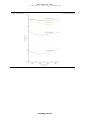
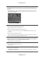
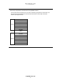
PolyMUMPs
FAQ
a MUMPs® process
MEMSCAP
Revision 2.0
PolyMUMPs FAQ, v2.0
1
Copyright © 2004 by MEMSCAP. All rights reserved.
Permission to use and copy for internal, noncommercial purposes is hereby granted. Any distribution of this
manual or associated layouts or any part thereof is strictly prohibited without prior written consent of MEMSCAP
Inc.
PolyMUMPs FAQ, v2.0
2
Introduction
Over the 10+ years of PolyMUMPs™, we have held numerous technical interactions with users of the process
regarding everything from “What can I make?” to “What is the temperature coefficient of resistance, elastic
modulus, and dielectric constant of each PolyMUMPs layer?”.
After sorting through hundreds of emails, we’ve compiled the most relevant and common question/answer
combinations in an attempt to establish a technical guide for Frequently Asked Questions. This is by no means a
complete guide; however it is an ongoing effort. Our hope is to add to this guide every year as more questions are
asked. For now, we hope our users will find this first version of the FAQ both valuable and educational as a
foundation for technical guidance on PolyMUMPs. Ideally, this information will lead to more questions that delve
further into one of the topics or spin-off into a new topic, which could be added to future revisions of this
ongoing, work-in-progress document..
Note: The information in this document is strictly advisory.
PolyMUMPs FAQ, v2.0
3
1 . 0
P O L Y M U M P S F A Q
M A T E R I A L D A T A A N D P R O P E R T I E S
1.0 MATERIAL DATA AND PROPERTIES, STRESS, AND SPECIFIC POLYMUMPS LAYER
INFORMATION
Numerous users over the years have asked for detailed material data and properties information, many of which
we have not characterized. Some of the most common questions are listed below.
YOUNG’S MODULUS OF POLYSILICON
What is the typical elastic constant value of PolyMUMPs polysilicon film? Does elastic constant of
polysilicon film vary each run or stay almost the same?
TCR, DIELECTRIC CONSTANT, ELASTIC MODULUS AND OTHER MATERIALS PROPERTIES OF
LAYERS WITHIN POLYMUMPS
Do you have information on the temperature coefficient of resistivity (TCR), elastic modulus, and dielectric
constant of the PolyMUMPs layers?
TYPICAL AND MAXIMUM LEVELS FOR STRESS AND STRESS GRADIENTS
What are the typical and maximum levels for stress and stress gradients?
We do not routinely measure Young's Modulus of the polysilicon. Past results on die fabricated on
PolyMUMPs by Johns Hopkins University have suggested that it is fairly stable. See the following
website for more information on their findings:
http://titan.me.jhu.edu/~sharpe/.
For other data, such as TCR, dielectric constant, stress gradients, and elastic modulus, we
recommend using published values as a fair approximation. The following websites might also be
helpful:
http://www.memsnet.org,
http://www.sfu.ca/adm/.
SUBSTRATE RESITIVITY
What is the resistivity value for the substrates used in PolyMUMPs?
The resistivity of the starting substrate used in PolyMUMPs is 1-2 Ohm-cm. However, the surface is
POCl3-doped in the first step of the process. After POCL3 doping, the surface of the substrate is 910 Ohm/Square.
STRESS DATA ON WEBSITE
Does the stress data on the website refer to residual stress?
Yes.
Is the residual stress data for Metal on the PolyMUMPs Run Data web pages for the gold itself or the gold
on Poly2 combo?
The data is listed by the individual layer so It's for the Cr/Au stack by itself.
PolyMUMPs FAQ, v2.0
4
1 . 0
P O L Y M U M P S F A Q
M A T E R I A L D A T A A N D P R O P E R T I E S
SURFACE ROUGHNESS OF POLY
What is the average surface roughness of the Poly 0, Poly 1, and Poly 2 layers?
AFTER ANNEALING:
P0: Ra = 9.93 nm Rrms = 12.12
P1: Ra = 9.99 nm Rrms = 12.55
P2: we don't have Poly2 surface roughness, but it should be between the Poly0 and Poly1 values.
ABOUT METAL COMPOSITION
What is the metal composition in PolyMUMPs?
The nominal (or target) thicknesses are 200A Cr and 5000A Au.
ABOUT OXIDE THICKNESS ACCURACY
How accurate is the oxide, as deposited?
The oxide thickness is 0.75 um +/- 12.5%.
GOLD PURITY AND COMPOSITION
What is the typical purity of the gold used?
Purity of Au is 99.999%.
OPTICAL CONSTANTS OF THE NITRIDE AND POLY LAYERS
Index of refraction of Nitride = 2.19
Index of refraction of PSG = ~1.46 (varies depending on exact P content)
STRESS MEASUREMENT METHODOLOGY
How are the stress levels measured for the PolyMUMPs layers?
We perform wafer bow measurements on monitor wafers, and calculate a residual stress.
PolyMUMPs FAQ, v2.0
5
1 . 0
P O L Y M U M P S F A Q
M A T E R I A L D A T A A N D P R O P E R T I E S
METAL LAYER REFLECTIVITY
PolyMUMPs FAQ, v2.0
6
2 . 0
P O L Y M U M P S F A Q
G A L V A N I C A T T A C K E F F E C T
2.0 GALVANIC ATTACK EFFECT
Galvanic Attack became a hot-button issue early last year when several customers encountered severe staining or
discoloration of their devices where large metal pads were fabricated near Poly0 features. Feedback from these
customers led to a design rule revision to include a section on this phenomenon. Below are some of the
questions/answers
GALVANIC ATTACK ON POLY0 LEADING TO OPEN CONNECTIONS
Can the preferential etching of POLY0 lead to open connections?
Yes, from time to time we do see an open caused by this galvanic attack.
Are nitride breaches a good way to protect the POLY0 layers? If so, how does the nitride breach protect
the POLY0?
Any way to ground the Poly is a good way to eliminate the galvanic attack. Some customers (nonMUMPs) use metal lines to ground the poly to the dicing streets. This metal is then removed during
the dicing process. Other customers create thin fuses of metal to short the poly layers. The first time
they actuate their device they drive enough current through the device that the fuse opens or breaks.
DEPENDENCY OF GALVANIC ATTACK ON METAL AND POLY
Please elaborate a little bit about the dependency of the galvanic attack on the metal and poly design.
Dilute HF attacks the poly during the DI rinse of the release step. It occurs more in areas where
metal is close to exposed poly, especially Poly0. It also attacks Poly1, but to a lesser degree. It’s an
electrochemical attack that is caused by a potential between the Au and the poly. If the poly can be
grounded, it greatly reduces or eliminates the attack.
THICK OXIDE REMAINING AFTER RELEASE
We have observed VERY thick (~30 nm) name oxides after release of our PolyMUMPs structures. The
chemical analysis of the film doesn't show anything unusual, yet we see layers that are an order of
magnitude thicker than we expect. Is this an issue that your fabrication people are aware of and if so, do
you have thoughts on its origin?
The prevailing hypothesis is that the Cr/Au metal produces a galvanic potential that drives oxidation
of the polysilicon. Before release, the thickness is approximately 10-25A. However, there are
indications that due to the galvanic attack that can occur during the release (dependant on metal &
poly designs), the native oxide may be get to be about 200A thick.
DISCOLORATION OF POLY1 AND POLY2
I've got a lot of Poly1 thermal actuators that appear to have a dark red color. Moreover, other Poly1 and
Poly2 polysilicon structures around them are not discolored. The actuators with strange colors have very
high resistance, while those without discoloration work fine. The color variation is apparent prior to release.
The problem is due to the galvanic potential caused by the gold on the polysilicon. The high work
function of the gold sets up an electrochemical potential in HF that leads to preferential attack of the
polysilicon particularly along grain boundaries. This problem is always more pronounced when
there are large gold pads. The discoloration and high resistance is caused by preferential attack of
the polysilicon grain boundaries in the HF release step. Even a BOE will cause this problem if there
is enough gold. We do a BOE cleanup of the wafers before they are shipped and this can expose
the Poly1. This is most likely why they are discolored before you do the release. One indication of
the processing is to look at the poly1 resonator we put in the lower left hand corner of your chips.
These have smaller gold pads but can still exhibit some discoloration. The only way to completely
avoid this problem is eliminate metal from your design entirely. Since this is not very practical, we
recommend placing a safe distance between susceptible features in your design
PolyMUMPs FAQ, v2.0
7
2 . 0
P O L Y M U M P S F A Q
G A L V A N I C A T T A C K E F F E C T
POLYSILICON DISCOLORING PROBLEM – AU GALVANIC EFFECT
Would you please give me some references which talk about this HF attack of poly in Au/Poly system?
Also, for future runs, could you please give me some advice on designing structures with Au pads and
wirings?
The galvanic effect associated with gold on polysilicon can be very unpredictable. The best way to
avoid it is to minimize or eliminate the gold. You might also try longer leads to the actuators.
Please refer to the design rules for more information on this topic. Another source is:
(L. Torcheux, A. Mayeux, M. Chemla, Electrochemical coupling effects on the (corrosion of silicon
samples in HF solutions, (J. Electrochem. Soc.)(, vol. 142, no. 6,) (pp. 2037-2046, June 1995.)
DISCOLORATION OF STRUCTURES ON THE SAME POLY1 LAYER
Looking at some unreleased die (with photoresist protective coat removed), we noticed that two objects
that were on the same layer (Poly 1) looked very different in color. Normally we don't pay any attention to
that, but these seemed to be alternating whitish gray (the indicators) and purple with blue edges (the
thermal actuators). Is there any reason for that?
The color variations may be oxide (PSG) thickness variations over the Poly1 structures. After
metallization, the wafers are processed in a cleaning step which removes about 0.5um of the top
PSG layer. Electro-chemical effects during this wet etch can cause differential etching of poly
features electrically connected Au/Cr structures on the die. (This effect is usually seen most clearly
after a wet HF release step)..
PolyMUMPs FAQ, v2.0
8
P O L Y M U M P S F A Q
3 . 0 P R O C E S S
3.0 PROCESS
We get lots of specific questions about the process; how it’s fabricated, what tools are used, effect of one mask
level on another, are just some of the topics. The section below lists the most common questions/answers on this
topic.
SIDEWALL THICKNESS OF OXIDE2
Is the sidewall thickness of Oxide2 the same as the film thickness (0.75µm), or are the sidewalls thinner?
The sidewall thickness should be the same as the film thickness.
METHOD OF GOLD DEPOSITION
How is the gold deposited?
It is evaporated in an e-beam tool
ETCHING EFFECT OF P1_P2_VIA
What is the total oxide thickness removed during the P1-P2 via etch? If 2nd oxide layer is directly on 1st
oxide layer and these layers (1st and 2nd layers) are etched by using P1-P2 via etch, are these layers
etched away entirely?
The P1_P2_Via etch will remove approximately 1.1 um of PSG.
THICKNESS OF PSG FILMS CAUSING STRESS GRADIENT
Polysilicon films are doped with phosphorous from the PSG layers both above and below it. Thicknesses
of these PSG films are different. PSG below polysilicon is 10 times thicker than the above one. Does this
cause any unsymmetrical doping profile or stress gradient in polysilicon?
There is a slight stress gradient in the layers. A slight upward bow is observed in released
cantilevers on test structures. The degree of bow is dependant upon the layer.
REASON FOR PHOSPOROUS DOPING OF WAFER SURFACE
The surface of the wafers is first heavily doped with Phosphorus. What is the aim of this process??
Charge feed through can occur at high voltages. The surface of the substrate is heavily doped to
ensure that there is minimal charge build-up at the nitride-substrate interface.
THERMAL TREATMENT THROUGHOUT MUMPS
What is the history of thermal treatment throughout PolyMUMPs?
There are four 1-hour anneals at 1050 C. These occur after the first PSG deposition, after poly1
deposition, after the second PSG deposition, and after the poly 2 deposition.
RINSES BETWEEN HF AND CO2
Are there any rinses in between the standard HF release and the supercritical CO2 drying?
We do a DI water rinse after HF release, followed by a IPA rinse to remove the water prior to CO2
CONTROL DOPING OF POLYSILICON LAYERS
Is it possible to control the doping area of the polysilicon layers in PolyMUMPs? Can I deposit the PSG
oxide on the polysilicon only on certain areas.
No, it is not possible to control doping in PolyMUMPs.
PolyMUMPs FAQ, v2.0
9
P O L Y M U M P S F A Q
3 . 0 P R O C E S S
LPCVD ON POLY1
What temperature is used for the LPCVD on poly 1? Do you have an idea as to what the grain size is in
the as-deposited film? Do you have an idea as to how much phosphorus gets into this film from the top
and bottom?
Poly is deposited at 580 C. The cross section below demonstrates the film morphology. The relative
amount of doping from the upper and lower PSG depends on the structure and how much or if any
PSG is above or below the film.
ETCH RATES IN HF
What is the etch rate of PSG (sacrificial layer) in 49% HF?
Etch rate of PSG in 49% HF is 10-20um per minute
What is the etch rate of PSG (sacrificial layer) in 10:1 Buffered HF?
According to our daily SPC monitoring, the etch rate of PolyMUMPS PSG in buffered HF solution is
42(+/-3)A/sec.
What is the etch rate of the polysilicon in 49%HF?
It is so slow that we have never measured it. However, if you leave doped poly in HF for a long time
(45 min - 1 hour) it will etch along the grain boundaries and crack.
OXIDE2 REMOVAL
You place oxide on top of POLY2 to perform the doping, pattern the poly, anneals, and then remove it by
RIE prior to metallization. How does this oxide removal etch affect the OXIDE 2 layer in the field areas,
specifically how much of the 0.7 um of OXIDE 2 gets etched in the process?
Approximately 3000A of Oxide2 gets etched..
DOPING CONCENTRATION OF POLY1
What is the doping concentration value of Poly1?
Approximately 1E19.
TEMPERATURE OF METAL DEPOSITION
At what temperature is gold deposited?
The estimated maximum temperature is 110C. We do not have a direct measurement, but this is the
best estimate with some indirect info.
PolyMUMPs FAQ, v2.0
10
P O L Y M U M P S F A Q
3 . 0 P R O C E S S
BACKSIDE DEPOSITION OF SUBSTRATES
What exactly is deposited on the back side of the PolyMUMPs wafers??
All of the films that are deposited on the front side of the wafer get deposited on the backside. The
Poly and LSN are approximately the same thickness but the PSG is about 40% of front side
thickness (see diagram below).
Poly2 HM (PSG) 2000 A
Poly2 15000 A
2nd Oxide (PSG) 7500 A
Frontside
Poly1 HM 2000A
Poly1 20000A
1st OXIDE (PSG) 20000A
Poly 5000A
LSN 6000A
Wafer
LSN 6000A
Poly 5000A
1st OXIDE (PSG) ~8000A
Backside
Poly1 20000A
Poly1 HM ~800A
2nd Oxide (PSG) ~3000 A
Poly2 15000 A
Poly2 HM (PSG) ~800 A
..
PolyMUMPs FAQ, v2.0
11
4 . 0
P O L Y M U M P S F A Q
L A Y O U T A N D D E S I G N R U L E S
4.0 LAYOUT AND DESIGN RULES
The design rule documents are meant to be a comprehensive guide to PolyMUMPs, however some rules can be
confusing. There are also intricacies of the layout process which need deeper explanations. Below are
questions/answers which ask for further clarification of some of these rules and layout issues.
POLY 2 ENCLOSING METAL RULE
To clarify the rule of Poly2 enclosing metal: does this refer to the outer perimeter of a poly2 polygon in
reference to the outer perimeter of the metal?
Yes. The poly2 polygon must extend beyond the metal polygon as shown in the figure for rule M
STACKED HOLES IN POLY2 AND METAL
If you have stacked holes in poly2 and metal, the metal hole should overlap the poly2 hole as per design
rules - correct? (i.e. in this case the poly2 overlap would only be 2 um instead of 3um as per rule M).
Metal holes must enclose poly2 holes by 2 um (rule U), in other words, the metal should be a
minimum of 2 um from the edge of the poly2 hole.
METAL ON POLY1
Is there any way of laying down metal on POLY1 instead of POLY2? The design rules state that due to
the absence of an oxide level POLY2 is best, but using a via couldn't POLY1 have the same top layer
traits (etch away 2nd Oxide)?
Actually there is NO way to put metal on Poly1. There is no way to expose the Poly1 in the process
for metallization without first etching it away. To expose the Poly1 you have to perform a VIA cut
that removes the oxide. This then leaves the poly1 exposed during the Poly2 etch resulting in
complete etch away of the Poly1.
RELATIONSHIP BETWEEN HOLE AND STRUCTURE LAYERS IN POLYMUMPS
Please expand on how HOLE0, HOLE1, HOLE2 and HOLEM for POLY0, POLY1, POLY2 and METAL are
used and what they are?
The holes are used to put etch holes in the poly and metal layers. In some tools it is difficult to make
the etch holes, so we have added these layers to facilitate that task. If there is a poly0 feature that
has a hole0 feature on top of it, there will not be any poly0 at the point where the hole0 feature is.
When the masks are made, the two layers are combined together by the operation poly0 not hole0.
MASK USAGE
Is a single mask used or a stepper to pattern from a single reticle?
One mask is fabricated for each photo level - one set is used per run.
AUTOCAD LINE COMMANDS
Can I draw a design with "line command" of AutoCAD, then convert it into a GDSII file and assume
everything will be OK?
The line command should be fine as long as the areas are closed properly. It is always best to look
at the gds file to make sure it is what you expected after the conversion.
PolyMUMPs FAQ, v2.0
12
4 . 0
P O L Y M U M P S F A Q
L A Y O U T A N D D E S I G N R U L E S
CREATING L-SHAPED FEATURES
Are boxes allowed to overlap? For example to make an "L" shape out of poly1 do I need to make 2
abutting boxes of poly 1 or can the boxes overlap?
Polygons can and should overlap.
TOLERANCES OF LINES AND FEATURES WHEN LAYOUT BURNED TO MASK
What is the dispersion of the initial design value due to the layout (and maybe process)? A line of X um
wide on the design will be in reality X um +/- 0.1um, for example.
The actual line would be x um +/- .15 um for vertical and horizontal lines. It will be worse for rotated
features, perhaps +/- .4um? This is only for the mask - not process tolerances.
0.25UM GRID IN LAYOUT
One of my structures doesn't readily adhere to the .25 um grid that the user manual says it should. If that
structure is still included in my final design what will happen to the area that doesn't adhere (this is due to
rotation by 45 degrees)? Will it truncate the small area that overlaps or will it do something else?
Nothing serious will happen. The only thing to be aware of is that the objects you draw that are not
on the 0.25um grid will snap to a .25um grid. So the objects may be slightly bigger or smaller than
expected.
EXACT DIE DIMENSIONS
What are the exact die dimensions on the mask layout, before dicing?
Standard die size is 10.15mm x 10.15mm; once the dies are diced from the wafer, then it's 10.1mm
+/- .025mm. Any subdicing cuts will reduce the chip size by 50um on each side of the subdicing line.
What is the actual die size when all are laid out on the mask?
The die size is 10150 before dicing. There is a 10150 micron pitch between chips so in essence a 75
micron frame around each die. Approximately 25 microns per side is diced from that to give a die of
10100 microns.
ALIGNMENT OF DESIGN WITHIN 1CM X 1CM SPACE
Does it play a role, where the structures are within the die location, if the whole area is 10000um x
10000µm at the end? Is it necessary to draw the edges of the die?
It does not matter where the structures are placed within the file as long as they are all within a
1cmx1cm area. The top level cell of all designs will be placed in the center of the die space. Edges
don’t need to be drawn.
CONVERTING AUTOCAD FILES FOR POLYMUMPS
Is there a way to convert AutoCAD files to formats acceptable for MUMPs?
All MUMPs submissions must be in either GDS or CIF format. AutoCAD can import and export in
DXF format. There are a few commercial software can convert between DXF and GDSII, and GDSII
is supported by MEMS Pro & Tanner tools. The two converters we've evaluated are:
1. Artwork Conversion
http://www.artwork.com/tanner/dxf/index.htm
2. LinkCAD
http://www.linkcad.com/index.asp?in=/linkcad/
PolyMUMPs FAQ, v2.0
13
5 . 0
C A N
I
P O L Y M U M P S F A Q
D O T H I S A N D W I L L
I T
W O R K ?
5.0 CAN I DO THIS AND WILL IT WORK?
Probably the most popular question we receive is:
“If I want to do ‘X’, can I combine ‘LAYERA’ with ‘LAYERB’, and will it work?”
Most of the time, there isn’t a definite answer because every design has unique needs. We simply can’t accurately
predict what the result or performance of every design will be. Our approach to these kinds of questions is to
provide a caveat that the answers are merely suggestions based on our experience with PolyMUMPs, meant to
give the user more data prior to fabrication. Below are questions/answers we’ve provided.
STACKING OXIDES
If I stack Oxide1 and Oxide2 on top of each other and then use Poly1_Poly2_Via, is this going to etch only
Oxide2 or both layers?
The via etch will etch all of the Oxide2 and some of Oxide1 because of the overetch done in the via
etch
DIMPLES IN POLY2
I am wondering whether I can have dimples in the POLY2 layer. Specifically, the structure that I have in
mind is to draw POLY0, draw DIMPLEs, and then draw POLY2, without drawing POLY1 at all. I am hoping
to obtain a layer of polysilicon with dimples on the bottom side, such that I can deposit metal on top of the
layer. Is this a reasonable structure?
DIMPLES can be drawn for use in the poly2 layer but you do run the risk of a poly1 stringer
occurring in the dimple hole. (note you are etching all the poly1 from the dimple hole, see section
2.3.2 of the design rules as an explanation) An alternate way to do this would be to use P1_P2_Via
for the dimple. This will etch about 1.3-1.5 um deep into the stack of oxide1 and oxide2.
USABLE STRUCTURE LAYERS
Can I use a polysilicon ground layer( POLY0) as a structure layer?
Poly 0 is attached to the nitride layer and cannot be used as a moving part
Is the PolyMUMPs Metal suitable for structures, such as staples?
Metal cannot be used as a structural member. The step coverage is inadequate
MAXIMUM STRUCTURE SIZE
How large of structures without deformation can we make in PolyMUMPs?
It is almost impossible to unequivocally state maximum structure sizes in PolyMUMPs. It is
dependant upon several aspects of the design; feature layer, method of release, mechanical
stiffness of structure, and type of mechanical support are some of the factors.
GUIDELINES FOR RELATIONSHIP BETWEEN BEAM WIDTH AND ETCH HOLES
What are mass/wide beam dimension on that one has to use etching-hole? What is the best etching-hole
dimensions and placement on such a wide beam /mass?
Greater than 50 microns should have etch holes. The etch holes should be at least 3 microns
squared and placed evenly along the beam.
PolyMUMPs FAQ, v2.0
14
5 . 0
C A N
I
P O L Y M U M P S F A Q
D O T H I S A N D W I L L
I T
W O R K ?
ELECTRICAL CONTACT ISSUES WITH POLYSI BEAMS
Two Poly1 switch beams (e.g. 2 micron width x 200 width length) don't seem to be making electrical
contact when touched together at their ends. Do you have any easy answers to what the problem might
be, and any suggestions for making electrical contact between PolyMUMPS PolySi beams?
Polysilicon electrical contacts made without a lot of force can result in high resistance due to native
oxide as well as imperfections in the sidewall (i.e., not perfectly smooth). Increasing the contact area
and the force should help. Also, you might try increasing the test voltage. We've seen contact
resistance decrease as the voltage goes up.
MAXIMUM BEAM WIDTHS
What is the maximum width beam without release holes to meet the requirement of etching away
all the underneath oxide layer?
We estimate a maximum of 50um to have all the oxide etched away, using the standard PolyMUMPs
HF Release process.
MINIMUM ANCHOR FEATURES
What is the minimum anchor width and length from the mechanical strength point of view?
3 um width and length anchors should work for small masses.
More information on this topic can be found in a paper by Sandia Laboratories (“Shock Testing of
Surface Micromachined MEMS Devices”; authors: Michelle A. Duesterhaus Vesta I. Bateman,
Darren A. Hoke)
POLY ANCHORED TO NITRIDE SURVIVING RELEASE
Do you see any problem if structural Poly is anchored to nitride during the release?
No, there is no problem with this method.
ANCHOR1-NITRIDE STACK
If I stack Anchor1 on Nitride, will the Nitride etch away?
The anchor will roughen the nitride somewhat, but will not etch through it.
ETCH DEPTH WHEN USING ANCHOR2 LEVEL
What happens when one utilizes the mask ANCHOR2 above a POLY1 layer? Does the etch stop at
POLY1 or does it go through until it reaches POLY0 or Nitride?
The etch will stop on the poly1. It may roughen the surface a bit.
CONNECTING POLYS
How do I put Poly1 on top of Poly0 without an oxide layer between them?
In order to put Poly1 on top of Poly0, use the Anchor1. Anchor1 provides holes to be filled by Poly1.
Once Poly1 fills in the holes there is a connection between Poly1 and Poly0. You may also use
Anchor 1 to connect Poly1 to Nitride.
UNDERETCHING PSG
I am trying to assess whether your PolyMUMPs process can provide an insulating layer between Poly1
and Poly2 by virtue of a technique called "under-etching". In under-etching, the sacrificial layers can be
"selectively" removed such that parts may be left behind in order to provide insulating support posts, for
example supporting a Poly1 cantilever over Poly0, or a Poly2 cantilever over Poly1.
This may be possible if you make the poly structures extra large such that the 2.5 min HF
release(done at our facility) will not remove all of the PSG.
PolyMUMPs FAQ, v2.0
15
5 . 0
C A N
I
P O L Y M U M P S F A Q
D O T H I S A N D W I L L
I T
W O R K ?
DIMPLE SPACING AND SIZING GUIDELINES
Can you please provide some tips to avoid stiction when designing comb drives?
We recommend using dimples, which are little bumps in the poly layer to keep it from touching the
surface in large areas. There will be only a point contact and consequently less area to stick to.
How far apart and how large should the dimples in Poly1 be to get minimum stiction? Is it possible to have
too many dimples?
In general, add dimples to anything that moves. We recommend a minimum size of 4um x 4um.
The use and effectiveness of dimples is entirely design dependant.
How about dimples for double-thickness structures?
4 micron dimples in the dimple layer is recommended for double thickness structures.
How about dimples in Poly2 where there is no underlying Poly1?
Any etch or combination of etches in poly1poly2via, or dimple would effectively make a dimple in
poly2. The dimple etch by itself would probably make a very slight, ineffective dimple in poly2.. The
poly1poly2via/dimple combination is another possible approach.
DOUBLE-THICKNESS POLY STRUCTURES
Any more advice on double-thickness poly structures?
A rule of thumb for doubled-stacked poly lines is to make the width greater than or equal to the
thickness of the stack. Therefore, the minimum width size for double stacked poly should be 3.5 um
or even 4.0 um to be safe. During the metal lift-off process, ultrasonics are used to remove the
metal. Any feature with less than a 1 to 1 thickness to width ratio, is more likely to break apart in the
bath.
How can I make a ~4um thick, (poly1 + poly2) structure? And will it have flat side edges?
You can do double stacked poly to achieve 3.5um but not 4um, according to the technique explained
in the DR. Edges will be fairly flat.
Can we use Poly1_poly2_VIA to anchor Poly2 on Poly1 and then deposit Metal atop Poly2?
If the poly2 is larger than the via and the poly1 then it will work fine. The thing to be careful of is if the
via is larger then the poly1 then the poly1 will get etched wherever the poly2 gets etched. This could
cause a short if you are not careful. This is the double poly structures mentioned in the design rules.
When using the Poly1/Poly2 stack technique, some of the beams created with this double layer becomes
discontinuous (before release). These beams are pretty narrow, at the minimum feature size of 2 um. Is
this a typical result of the stack technique?
This is not caused by the Poly2 etch. This is caused by the ultra-sonics used during the metalization
step. The aspect ratio of a 2um wide beam consisting of both Poly1 and Poly2 is too high and it
breaks off when in the lift-off. When designing for double-thickness Poly structures, we recommend
limiting the aspect ratio to 1:1 (i.e. 3.5 um wide beam for structures made of both poly1 & 2).
PolyMUMPs FAQ, v2.0
16
5 . 0
C A N
I
P O L Y M U M P S F A Q
D O T H I S A N D W I L L
I T
W O R K ?
METAL ON OXIDE
Is it possible that the second oxide, (which is designed to be released) could be masked on some areas of
the wafer so that it doesn't get released? If this is possible, could we deposit the metal (gold) on top of this
oxide, or are there stiction problems?
In PolyMUMPs, the only way to keep the second oxide from releasing is to sandwich it between
poly1 and poly2. You will likely see adhesion problems when putting gold directly on the oxide.
OXIDE ON POLY AND STRESS
If a device (Comb drive) is manufactured but not released, could we oxidize the top part of the polysilicon
without generating stresses on the structures (e.g., will the fingers bend up or down)?
It will likely get stressed during an oxidation and once it is released, the fingers would deflect up or
down
OXIDE2 ETCH BETWEEN POLY1 AND POLY2 PLATES
I plan to fabricate 120x120 um2 Poly2 plate and 120x120 um2 Poly1 plate, and I’m wondering whether the
Oxide2 layer between Poly1 and Poly2 plate be released using HF? How fast would it etch?
Yes, but we recommend putting release holes in the Poly2 layer to reduce the release time.
Otherwise a 10 min release in 49% HF should easily undercut 60um on a side and release it.
FABRICATING LARGE SUSPENDED PLATES
I would like to know if trying to make suspended plates of over 500 x 500 micrometers is too big for the
PolyMUMPs process due to residual stress. These plates would be coated with gold (except for the etch
holes).
We believe stress in the Cr/Au will likely bow up the edges significantly on plates of this size.
PolyMUMPs FAQ, v2.0
17
P O L Y M U M P S F A Q
6 . 0 M I S C E L L A N E O U S
6.0 MISCELLANEOUS
WIRING LAYOUT STANDARDS
Are there any standards to define the size of the wiring of the device (in terms of width and gap distance
between 2 wires) and bond pads (area and shape), and if so what are they?
With regard to wiring, 10 micron wires with a 5 micron space is fairly conservative. More experienced
MUMPs designers have been successful with 5 micron wires and 3 micron spaces. For bond pads,
100 square micron pads with 50 micron space are probably more than adequate.
SUBMITTING DESIGNS LARGER THAN 1CM X1CM
Is it possible to get a larger die size than the standard? E.g. 2 cm x 2 cm?
Yes, it is possible to have a larger die size but there would be extra costs in addition to just the die
location cost due to the added time required to dice and sort the wafers into the individual die
locations.
DO I NEED CO2 DRY? HOW DO I KNOW?
How do I know if I should use the supercritical CO2 dry?
Supercritical CO2 Dry is offered as a solution to device stiction. It's hard to say whether or not you
need it as each design is different. There's really no risk in the decision as customers can send their
finished chips back to us for CO2 dry if they observe a great deal of stiction.
CHANGING OR MODIFYING THE PROCESS, LAYER THICKNESSES, AND SEQUENCES
Can I have a thicker material layer or different process sequence in PolyMUMPs? How about additional
layers?
Modifying the process either with different layer thicknesses or process sequences is NOT possible
as part of the regular PolyMUMPs runs – a custom run would be required.
However, several customers have successfully added layers or process steps on top of a regular
PolyMUMPs run. These modifications are quoted separately from, and in advanced of, the requested
PolyMUMPs run.
DIE VARIATION
Do the 15 shipped die come from 15 different wafers?
Usually, though sometimes we will replicate die on a run mask set when the run is not full.
TESTING RESONATOR ON MUMPS DIE
What are the recommended procedures and parameters for testing the corner test die, as required in each
PolyMUMPs design?
Conditions are as follows:
50 Vdc offset (on groundplane)
+/- 8 Vac bias one side only
POLYMUMPS CHIP STORAGE
What kind of environment do you recommend for storage of PolyMUMPs chips?
Our fab environment is controlled at about 45% RH. We consider this essentially safe to store
material indefinitely. 25%-50% would probably be fine. You can buy a desiccant that will absorb
more moisture if you want to dry out the dry box more. Be aware, very low humidity's (<30%) can
lead to ESD problems, so be careful when they are handled after storage.
PolyMUMPs FAQ, v2.0
18
P O L Y M U M P S F A Q
6 . 0 M I S C E L L A N E O U S
EFFECTS OF MOISTURE AND HUMIDITY ON POLYSILICON
Is a cantilever made of Poly sensitive to moisture & humidity?
We have not done any humidity characterization of poly structures. However, we normally keep our
chips either under vacuum in anti-static bags or in a nitrogen box.
PHOTORESIST APPLIED AFTER METAL
Is the photoresist that is spun on the chip after metal for protection cured?
No, it can easily be stripped with Acetone. Directions to do so are included with die shipment.
SHIPPING AND STORAGE OF CHIPS THAT HAVE UNDERGONE RELEASE/CO2 DRY AT MEMSCAP
How are chips shipped that have undergone HF Release/Supercritical CO2 Dry at your facility? What kind
of environment is best for long term storage of these chips at my facility?
Released chips are shipped on UV tape on dicing ring in conductive, light-tight clamshell carriers.
The UV tape is to assist in removal should sticking occurs (this has been observed in the past for
long-term storage of critical-point-dried die by several companies). The UV tape also has an
expiration date associated with it to motivate removal of chips to another medium after shipping.
Safest of these is probably a waffle pack sorted in a clean room environment. We moved away from
Gel-Paks and developed this medium for shipping because Gel-Pak does not recommend long-term
storage in a standard Gel-Pak (adhesion increases over time and moisture absorption). This is
accelerated by the cleaned surface resulting from CPD.
PolyMUMPs FAQ, v2.0
19