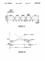
1
USO05295229A
United States Patent [191
[11] Patent Number:
Viot et al. '
[45]
[54] CIRCUIT AND METHOD FOR
Assistant Examiner-Tan'q R. Ha?z
Attorney, Agent, or Finn-Elizabeth A. Apperley
[21] Appl. No.: 899,975
[58]
[57]
Jun. 17, 1992
Int. Cl.5 ............................................ .. G06F 15/18
US. Cl. ............... ....................... .. 395/51; 395/3;
395/11; 395/900
Field of Search ..................... .. 395/3, 51, 900, 11,
395/61
[56]
References Cited
U.S. PATENT DOCUMENTS
4,694,418
9/1987
4,716,540
12/1987
4,860,243
8/1989
Ueno et al. ..
5,136,685
8/1992
Nagazumi
Yamakawa . . . . . . .
. . . . . ..
395/3
.... .. 395/3
. . . . . . ..
. . . . . ..
395/3
395/61
Hisano .................... .. 395/51
5,179,634
1/1993 Matsunaga et a1. .
5,189,636
2/1993
ABSTRACT
A circuit (14) and method which determine a degree of
membership of an input in a membership set during a
fuzzy logic operation. The degree of membership is
calculated by a single “MEM” software instruction.
The MEM instruction determines whether the system
input has a degree of membership of zero, of a satura
tion level, or of some value in between. An operand
assignment circuit (50) and an ALU (56) allow circuit
(14) to determine the degree of membership more
quickly. Assignment circuit (50) determines a multiplier
Ueno et a]. ........................... .. 395/3
5,148,977 9/ 1992 Hibino et al.
5,165,011 11/1992
“Creating Fuzzy Micros” in the Dec. 1991 issue of
Embedded Systems Programming, vol.v4, No. 12, pp.
1-10, written by James M. Sibigtroth.
User’s Manual entitled “FF-3000 Digital Fuzzy Proces
sor User's Manual” published by Omron Corporation.
Primary Examiner-Michael R. Fleming
[73] Assignee: Motorola, Inc., Schaumburg, Ill.
‘
Mar. 15, 1994
the Apr. 1992 issue of AI Expert, vol. 7 No. 4, pp. 25
[75] Inventors: .1. Greg Viot, Austin; James M.
Sibigtroth, Round Rock; James L.
Broseghini, Austin, all of Tex.
[51]
[52]
Date of Patent:
through 31, written by James M. Sibigtroth.
DETERMINING MEMBERSHIP IN A SET
DURING A FUZZY LOGIC OPERATION
[22] Filed:
5,295,229
395/51
Patti et a1. ......................... .. 364/786
for a multiplication operation based on a number of
signi?cant bits in the values to be multiplied. If the
multiplier is smaller than the multiplicand, shorter mul
tiplication operations may be performed. Additionally,
ALU (56) operates in a split mode of operation which is
able to perform two eight bit subtraction or multiplica
tion Operations concurrently which also results in these
operations being performed more efficiently.
OTHER PUBLICATIONS
“Implementing Fuzzy Expert Rules in Hardware” in
17 Claims, 7 Drawing Sheets
EXTERNAL BUS INTERFACE
INTERNAL MEMORY
CONTROL UNIT
20
:2
52
:2
we
TIMING
CIRCUIT
22
SEQUENCER
33
Q
INSTRUCTION DECODE
L 0610
&
MICRO ROM
CONTROL
BUS CONTROL
LOGIC
CLOCK
OSCILLATOR
2-4
POWER
CIRCUIT
CPU lg
0801 osc2
vDD
US. Patent
5,295,229
Sheet 1 of 7
Mar. 15, 1994
DEGREE
OF
“MEMBERSHIP
VERY
C0oL
‘00
2'0
3'0
4'0
HOT
WARM
WARM
5'0 - 6'0 68' 7'0
8'0
9'0
100
SYSTEM
INPUT
V
FIG.1
i"
/
/
\\//
//\\ \
/
-
/ lDELTA 1‘ * SLOPE 1
I
.
l
_ I
|
‘FF ______
05km]; SLOPE 2
SLOPE 1
_ SLOPE 2
/
\
$00
POINT 1
x
DELTA 1
V
FIG.2
POINT‘ 2
DELTA 2"
~
US. Patent
Mar. 15, 1994
Sheet 2 of '7
‘5,295,229
EXTERNAL
ADDRESS
QZHE. E50
AEI
WIN
.
mm,
A E\
MM
mm
noSQmmE2E8
@m2.05:
m.m?2%“8. E2
E0N.
1ZJ|.2<E15H mzoaHhswpmz 083 :29a; 6528‘
Hz:
EQDSm 4052
oH oA
‘H
*
mmP
1 zo?bouxm PHZD>
A.
3.3%
.m.AUNB
2
US. Patent
Mar. 15, 1994
Sheet 7 of 7
m
'
5,295,229
1
-
IF UPPER, 4‘ BITS OF DELTA 1=SD,
' DECQDE HEM
THEN Z1 FLAG IS ASSERTED
IF UPPER 4 BITS OF DELTA 2=$D,
THEN Z3‘ FLAG IS ASSERTED
USE INDEX REGISTER TO
ACCESS FIRST PAIR OF
1
IF z1=1. DELTA 1 IS WLTIPLIER 1
ELSE, SLOPE 1 Is MULTIPLIER 1
_ MEMBERSHIP FUNCTION OPERANDS
_ mo SLOPE 1 Is “ULTIPLICAND 1
(READ POINT 1 AND POINT 2)
1
INCREMENT ADDRESS IN
INDEX REGISTER BY TWO
CONCURRENTLY CALCULATE:
~
AND DELTA 1 IS NuLIIPLIcAND 1
IF Z3=1, DELTA 2 IS NULTIPLIER 2
AND SLOPE 2 IS NULTIPLIER 2
ELSE, SLOPE 2 IS NULTIPLIER 2 AND
DELTA 2 E WLTIPLICAND 2
DELTA 1=SYSTEM INPUT — POINT 1
I
DELTA 2=PDINT 2 - SYSTEM INPUT
I
CONCURRENTLY MULTIPLY:
DELTA 1 x SLOPE 1, AND
‘DELTA '2 x SLOPE 2
STORE DELTA 1 AND DELTA 2
VALUES IN DELTA REGISTER 6O
SET SATIRATION FLAGS:
I
SHIGH=1 IF A1 # 81> FF OR IF Z1=Z2=0
SLOW =1 IF A2 * S2) FF OR IF Z3=Z4=0
‘
SET JAM rues:
JHIGH=1 IF ZP2=1 AND SLOPE 1= 00
Jun’ =1 IF ZP4=1 AND SLOPE 2= 00
1
IF smH=sL0w =1, THEN RESULT=$FF
MEMBERSHIP FUNCTION OPERANDS
IE
(READ SLOPE 1 AND SLOPE 2)
4
ELSE RESULT’ A2 * 52
v
v
STORE RESULT IN
INCREMENT ADDRESS IN
INDEx REGISTER BY TWO
INTERNAL MEMORY 32
18
Y ES
ELTA 1(0?
DATA BUFFER 42 TO ‘0
FORCE RESULT IN 0]
1
IS
DELTA 2(0?
N0
A FORCE RESULT IN
DATA BUFFER 42 TO ‘00
Fl
8
1
5,295,229
2
Expert Rules in Hardware” by James M. Sibigtroth.
CIRCUIT AND METHOD FOR DETERMINING
MEMBERSHIP IN A SET DURING A FUZZY
LOGIC OPERATION
CROSS REFERENCE TO RELATED
APPLICATION
This application is related to a copending patent ap
plication ?led concurrently herewith and entitled: “A
CIRCUIT AND METHOD FOR EVALUATING s. . 0
FUZZY LOGIC RULES” by I. Greg Viot et al., Ser.
No. 07/899,968.
FIELD OF THE INVENTION
This invention relates generally to a data processing
system, and more particularly to execution of a fuzzy
logic operation in a data processing system.
BACKGROUND OF THE INVENTION
Data processors have been developed to function as
binary machines whose inputs and outputs are either
interpreted as ones or zeroes, and no other possibilities
may exist. While this works well in most situations,
sometimes an answer is not simply “yes” or “no,” but
something in between. A concept referred to as "fuzzy
logic” was developed to enable data processors based
on binary logic to provide an answer between “yes” and
The article was published in the April, 1992 issue of AI
EXPERT on pages 25 through 31.
Typically, the fuzzi?cation step has been imple
mented with software programs which are executed
either by a peripheral device or by a data processor.
Such software programs calculate a degree of member
ship using a mathematical equation which requires ex
tensive processing time. Therefore, although the soft
ware program provides an accurate result, the process
ing time generally limits the performance of a system in
which it is implemented. Another common software
solution implements a “table look-up” routine in which
a table of data stored in memory is accessed for a value
which corresponds to a particular input value. Al
though quicker than a mathematical calculation, the
table look up routine requires a large amount of dedi
cated memory which is expensive to implement. Hard
ware solutions to the implementation of the fuzn'?ca
tion step provide results even more quickly. However,
hardware solutions generally require a large amount of
dedicated circuitry which is in?exible. Although hard
ware solutions to the fuzzi?cation step are typically
faster than software implementations, hardware solu
tions require a large amount of dedicated circuit area
and are often too expensive to implement in a data pro
SInO.”
cessing system.
Fuzzy logic is a logic system which has membership
functions with fuzzy boundaries. Membership functions
translate subjective expressions, such as “temperature is
performing the fuzzi?cation step quickly, but without
costly hardware requirements. The speed typically as
warm,” into a value which typical data processors can
recognize. A label such as “warm” is used to identify a
range of input values whose boundaries are not points at
which the label is true on one side and false on the other
side. Rather, in a system which implements fuzzy logic,
the boundaries of the membership functions gradually
change and may overlap a boundary of an adjacent
membership set. Therefore, a degree of membership is
typically assigned to an input value. For example, given
two membership functions over a range of tempera
tures, an input temperature may fall in the overlapping
areas of both the functions labeled “cool” and “warm.”
Therefore, a need exists for a circuit or method for
sociated with a hardware solution is needed without the
memory usually associated with a software solution.
SUMMARY OF THE INVENTION
The previously mentioned needs are ful?lled with the ,
present invention. Accordingly, there is provided, in
one form, a circuit and method for performing a fuzzy
logic operation in a data processing system, the fuzzy
logic operation determining membership of an input
point in a predetermined membership set which is de
?ned by a plurality of boundary values. The method
includes the step of receiving a membership evaluation
instruction for initiating execution of the fuzzy logic
Further processing would then be required to deter
mine a degree of membership in each of the membership 45 operation in the data processing system. The member
ship evaluation instruction is decoded to provide a plu
functions (i.e. if the input temperature ?ts into each of
rality of control signals. A ?rst one of the plurality of
the membership sets, cool and warm).
boundary values is subtracted from the input value to
A step referred to as “fuzzi?cation” is used to relate
produce a ?rst delta value. The input value is concur
an input to a membership function in a system which
rently subtracted from a second one of the plurality of
implements fuzzy logic. The fuzzi?cation process at
taches concrete numerical values to subjective expres
sions such as “the temperature is warm.” These numeri
boundary values to produce a second delta value. The
?rst delta value and a third one of the plurality of
cal values attempt to provide a good approximation of
boundary values are multiplied to provide a ?rst result.
The second delta value and a fourth one of the plurality
of boundary values are concurrently multiplied to pro
human perception which is not generally limited to an
environment of absolute truths. After the fuzzi?cation
step, a rule evaluation step is executed. During execu
tion of the rule evaluation step, a technique referred to
as “min-max” inference is used to calculate numerical
conclusions to linguistic rules de?ned by a user. Conclu
sions from the rule evaluation step are referred to as
“fuzzy outputs” and may be true to varying degrees.
Thus, competing results may be produced. A last step in
vide a second result. The degree of membership signal is
provided to indicate that the input point is not included
in the predetermined membership set when either the
?rst delta value or the second delta value is less than
zero. The degree of membership signal is equal to a
minimum value of either the ?rst result, the second
result, or a ?fth one of the plurality of boundary values
the fuzzy logic process is referred to as “defuzzi?ca
if neither the ?rst delta value nor the second delta value
tion.” As the name implies, defuzzi?cation is the pro
is less than zero. ‘
cess of combining all of the fuzzy outputs into a com 65
These and other features, and advantages, will be
posite result which may be applied to a standard data
more clearly understood from the following detailed
processing system. For more information about fuzzy
description taken in conjunction with the accompany
logic, refer to an article entitled “Implementing Fuzzy
ing drawings. It is important to note the drawings are
3
5,295,229
4
temperature would have had a degree of membership of
not intended to represent the only form of the inven
tion.
$FF in the very warm membership set. Likewise, the
temperature of 75 degrees would have a degree of mem
BRIEF DESCRIPTION OF THE DRAWINGS
FIG. 1 illustrates in graph diagram form some of the
bership of $00 in the hot membership set. In the fuzzy
logic implementation of FIG. 1, a degree of member
concepts and basic terminology used to describe fuzzy
ship may range from a hexadecimal value of $00 to SFF,
logic;
which may corresponds to a fraction in a range of 0.00
to 0.996.
FIG. 2 illustrates a single membership set which may
FIG. 2 illustrates a membership set of FIG. 1 in
greater detail;
FIG. 3 illustrates in block diagram form a data pro
be represented by four values: Point 1, Point 2, Slope 1,
cessing system in accordance with the present inven
and Slope 2. A ?rst value referred to as “Delta 1” is
computed as the difference between a system input
tion;
(point “X”) and point 1. Similarly, a second value re
FIG. 4 illustrates in block diagram form an execution
ferred to as “Delta 2” is computed as the difference
FIG. 5 illustrates in logic circuit form a ?ag genera 15 between point 2 and the system input. From the compu
tation of the Delta 1 and Delta 2 values, the degree of
tion logic circuit of FIG. 4;
membership is provided in accordance with the method
FIG. 6 illustrates in block diagram form an operand
unit of FIG. 3;
assignment logic circuit of FIG. 4;
of the present invention. If a value of either Delta 1 or
Delta 2 is less than zero, then a degree of membership
FIG. 7 illustrates in block diagram form an arithmetic
logic unit of FIG. 4; and
20 for the corresponding membership set is 0.00. Other
FIG. 8 illustrates in flow chart form a ?ow of the
wise, the degree of membership is equal to the minimum
functions performed during execution of the MEM
value of either a product of Delta 1 and Slope 1, a prod
instruction in accordance with the invention described
herein.
uct of Delta 2 and Slope 2, or a saturation value. The
minimum value will be a degree of membership of the
25 current input value in the membership set being tested.
DETAILED DESCRIPTION OF A PREFERRED
EMBODIMENT
The present invention provides a circuit and a
method for “fuzzifying” an input to a data processing
system quickly and with a minimum amount of dedi 30
In the example described herein, the saturation value
has a hexadecimal value of SFF. However, other imple
mentations may allow a user of the fuzzy logic system
to choose a saturation value in accordance with the
speci?cations of a particular system. '
The instruction of the present invention, which is
cated circuitry. An instruction is provided which allows
referred to with the mnemonic label “MEM,” causes a
the user of the data processing system to perform the
data processing system to perform a series of steps to
fuzzi?cation step quickly without difficult and lengthy
determine a degree of membership of a system input
software programs. The fuzzi?cation step of a single
input label is encoded in the instruction which executes 35 value in one of a plurality of membership sets. Each of
the membership sets is characterized by a plurality of
quickly and efficiently without an excessive amount of
boundary values (Point 1, Point 2, Slope 1, and Slope 2)
added circuitry in the data processing system.
which are retrieved from memory. If each of the plural
During a description of the implementation of the
ity of boundary values has been appropriately stored in
invention, the terms “assert” and “negate,” and various
grammatical forms thereof, are used to avoid confusion 40 memory and if the system input value has been appro
priately stored in a register location prior to execution
when dealing with a mixture of “active high” and “ac
of the MEM instruction, a degree of membership of the
tive low” logic signals. “Assert” is used to refer to the
system input in one of the plurality of membership sets
rendering of a logic signal or register bit into its active,
may be determined. Subsequently, the degree of mem
or logically true, state. “Negate” is used to refer to the
rendering of a logic signal or register bit into its inac 45 bership of the system input in each of the plurality of
tive, or logically false state. Additionally, a hexadecimal
value may be indicated by a “S” symbol preceding a
value.
FIG. 1 provides a graph illustrating a few basic terms
and concepts of fuzzy logic. In the fuzzy logic system
membership sets is stored at a predetermined location in
memory. The implementation of the MEM instruction
allows a user of the data processing system to perform
a membership evaluation function more quickly than
traditional software implementations and with less dedi
cated circuit area than is required by typical hardware
described in FIG. 1, a “system input” is temperature in
implementations. For example, an arithmetic logic unit
degrees Fahrenheit. Five “membership functions” are
required for normal operation of the data processing
provided to relate labels to ranges of temperatures. For
system has been modi?ed to operate in a split mode of
example, from 0 degrees to 30 degrees, a temperature is
labeled “cold.” Similarly, from 20 degrees to 50 de 55 operation. Typically, the arithmetic logic unit is able to
perform a single sixteen bit operation at a predeter
grees, the temperature is labeled “cool.” Notice that the
mined point in time. However, the arithmetic logic unit
boundaries of each of the membership sets overlaps the
disclosed herein may be selectively enabled to either
boundaries of the adjacent sets. Therefore, a tempera
perform a single sixteen bit operation or two concurrent
ture may be in more than one set. For example, assume
eight bit operations. Therefore, arithmetic operations
that the system input indicates a temperature of 68 de—
necessary for calculation of a degree of membership in
grees. Referring to FIG. 1, notice that 68 degrees is
within the boundaries of both the warm and very warm
a membership set are concurrently calculated in less
time than would traditionally be required. Very little
membership sets, and a non-zero degree of membership
additional circuitry is required. To operate the arithme
in each of the membership sets may be obtained. The
system input has a degree of membership of $33 for the 65 tic logic unit in the split mode of operation, a single
enable signal is provided to an existing buffer circuit.
warm membership set and a degree of membership of
Additionally, only a small amount of added circuitry is
SCC for the very warm membership set. If the system
required to implement the MEM instruction.
input had indicated a temperature of 75 degrees, the
5
5,295,229
One implementation of the instruction and method of
operation described above is illustrated in FIG. 3. FIG.
3 shows a data processing system 10 in which the fuz
zi?cation instruction may be implemented. Data pro
cessing system 10 generally includes a central process
ing unit (CPU) 12, an oscillator 24, a power circuit 26,
a timing circuit 28, an external bus interface 30, and an
internal memory 32. CPU 12 generally has an execution
unit 14, a bus control logic circuit 16, an instruction
decode logic circuit 18, a control unit 20, and a se
quencer 22.
During operation, an “Osc 1” signal is provided to
oscillator 24 via an external source, such as a crystal.
6
plexor 54, an arithmetic logic unit (ALU) 56, a B-input
multiplexor 58, a ?rst data register 60, and a system
input register 64. Although not shown herein, it should
be apparent to one with ordinary skill in the art that
additionalregisters may be included in execution unit
14. For example, execution unit 14 may include an index
register or an accumulator. Additionally, in typical data
processing systems, system input register 64 may be
implemented as an accumulator.
‘
-
An External Information bus 40 provides address and
data information to data buffer 42. External Information
bus 40 receives the address and data information from
Internal Address bus 36 and Internal Data bus 34, re
The crystal is connected between the Osc 1 and Osc 2
signals to enable the crystal to oscillate. The Osc 1
provides a “Clock” signal to a remaining portion of data
processing system 10. Operation of a crystal oscillator is
well known in the data processing art and should be
apparent to one with ordinary skill in the art.
Similarly, power circuit 26 receives both a “Vdd” 20
ferred via External Information bus 40 to a remaining
portion of execution unit 14 via an Information Bus A
66 and an Information Bus B 68. Although not shown in
detail here, both Information Bus A 66 and Information
and a "Vss” signal from an external power source. The
through bit 0).
spectively. Data buffer 42 provides the values trans
Bus B 68 are sixteen bits wide and are divided into a
high side (bit 15 through bit 8) and a low side (bit 7
Vdd signal provides a positive 5 volts and the Vss signal
The low side of Information Bus A 66 is bidirection
provides a reference, or ground voltage. The Vdd and
ally coupled to a ?rst input of system input register 64.
Vss signals are provided to each of the remaining com
Similarly, the high side of Information Bus B 68 is bidi
ponents of data processing system 10. The routing of 25 rectionally coupled to a second input of system input
these signals is well known in data processing art and
register 64. A ?rst delta value referred to as “Delta 1”
should be obvious to one with ordinary skill in the art.
is provided to a first input of delta register 60 via a high
Timing circuit 28 receives the Clock signal and subse
side of Information Bus B 68. A second delta value,
quently provides appropriate timing signals to each of
“Delta 2,” is provided to a second input of delta register
CPU 12, external bus interface 30, and internal memory
60 via a low side of Information Bus B 68. Delta register
32 via a Timing Control bus 38.
A plurality of address values are provided from exter
nal bus interface 30 via an External Address bus 35.
Similarly, a plurality of data values are communicated
to external bus interface 30 via an External Data bus 33.
External bus interface 30 functions to communicate
address and data values between an external user and
60 is also connected to both Information Bus A 66 and
Information Bus B 68 to provide information to other
components of execution unit 14. Any additional regis
ters such as accumulators and index register would be
similarly coupled to Information Bus A 66 and Informa
tion Bus B 68.
Information Bus A 66 is connected to a ?rst input of
A-input multiplexor 54. An n-bit wide signal labeled
“Control” is provided to a second input of A-input
remaining portion of data processing system 10 via an 40 multiplexor 54, where n is an integer. A-input multi
Internal Address bus 36 and an Internal Data bus 34,
plexor 54 provides both a ?rst ten bit output labeled
data processing system 10. External bus interface 30
provides a plurality of address and data values to a
respectively. Internal memory 32 functions to store
“A-input Low Side” to a ?rst input of ALU 56 and a
second ten bit output labeled “A-input High Side” to a
second input of ALU 56.
values may be stored therein if speci?ed in a user pro 45
Information Bus B 68 is connected to an input of
gram provided via Internal Address bus 36 and Internal
B-input multiplexor 58. Control information necessary
Data bus 34.
to enable B-input multiplexor 58 to function correctly is
CPU 12 executes each of the instructions required
provided to a control input via a plurality of signals
information values necessary for the proper operation
of data processing system 10. Additionally, other data
during operation of data processing system 10. Internal
generated by the Micro-ROM (not shown) in control
Address bus 36 and Internal Data bus 34 communicate 50 unit 20 and transferred via Mircor-ROM Control bus
information between execution unit 14 and a remaining
65. B-input multiplexor 58 provides a ?rst ten bit output
portion of data processing system 10. Bus control logic
labeled “B-input Low side” to a third input of ALU 56.
circuit 16 fetches instructions and operands. Each of the
Additionally, B-input multiplexor 58 provides a second
instructions is then decoded by instruction decode logic
ten bit output labeled “B-input High side” to a fourth
circuit 18 and provided to control unit 20 and sequencer 55 input of ALU 56.
22. Control unit 20 and sequencer 22 maintain a se
quence of execution of each of the instructions to most
ef?ciently utilize the computing capabilities of data
processing system 10. Additionally, control unit 20
A signal labeled “Split Mode Control” is provided to
a fifth input of ALU 56. The Split Mode Control signal
is generated by the Micro-ROM memory in control unit
20 in response to execution of the MEM instruction.
includes a Micro-ROM memory (not shown) which 60 ALU 56 processes each of the inputs to provide a plu
provides a plurality of control information to each of
rality of results which are transferred via a Results bus
execution unit 14, bus control logic 16, and instruction
120. Results bus 120 provides a plurality of information
decode logic 18 via a Micro-ROM Control Bus 65.
values to each of result select logic circuit 46 and ?ag
Execution unit 14 is illustrated in greater detail in
generation logic circuit 48. Additionally, Results bus
FIG. 4. Execution unit 14 generally includes a data 65 120 is coupled to Information bus B 68.
buffer 42, a result select logic circuit 46, a ?ag genera
In addition to Results bus 120, ?ag generation logic
tion logic circuit 48, an operand assignment logic circuit
circuit 48 is coupled to both delta register 60 and data
50, an A-input control logic circuit 52, an A-input multi
buffer 42. Flag generation logic 48 receives a “Delta”
7
5,295,229
8
signal from delta register 60 and a “Buffered Data”
132 is labeled Jplow and is provided to a ?rst input of OR
signal from data buffer 42. Flag generation logic circuit
48 is also coupled to both operand assignment logic
gate 150.
circuit 50 and result select logic circuit 46 to provide a
B4) of the Buffered Data 2 signal are provided to NOR
gate 146. An output of NOR gate 146 is labeled “S4”
and is provided to a ?rst input of NOR gate 148.
plurality of flag values via a Flags bus 70. Additionally,
flag generation logic circuit 48 is coupled to ALU 56 to
‘
Additionally, bits seven through four (B7 through
provide a Jhigh and a 110,, signal to a sixth and seventh
Delta register 60 provides bits ?fteen through twelve
input of ALU 56, respectively.
Operand assignment logic circuit 50 is also connected
of a third information value to NOR gate 110. In this
implementation, the third information value is provided
to Information bus A 66, Information bus B 68, and 10 by a ?rst Delta signal referred to as a Delta 1 signal. An
output of NOR gate 110 is labeled “Z1” and is also
Flags bus 70. Operand assignment logic circuit 50 is
transferred via Flags bus 70. The Z1 signal is also pro
connected to A-input control logic circuit 52 to provide
vided to a second input of NOR gate 142.
both a ?rst input signal labeled “Multiplier 1” and a
second input signal labeled “Multiplier 2.” Addition
ally, operand assignment logic circuit 50 is coupled to
delta register 60 to receive the Delta signal. A-input
Similarly, delta register 60 provides bits seven
through four of a fourth information value to NOR gate
116. An output of NOR gate 116 is labeled “Z3” and is
transferred via Flags bus 70. The fourth information
control logic 52 is connected to A-input multiplexer 54
value is provided via a second Delta signal referred to
to provide the Control signal.
as the Delta 2 signal. The Z3 signal is also provided to
Result select logic 46 receives information via both
Flags bus 70 and Results bus 120. The information is 20 a second input of NOR gate 148.
Results bus 120 provides a NIaw and a Nhigh signal to
processed to provide a ?rst output labeled “Select” and
a ?rst and second input of OR gate 114, respectively.
a second output labeled “Force SFF.”
An output of OR gate 114 is labeled Nmem. The Nmm
Flag generation logic circuit 48 is illustrated in
signal is provided to a reset input (R) of both latch 130
greater detail in FIG. 5. Flag generation logic circuit 48
generally includes a NOR gate 110, a NOR gate 112, an 25 and latch 136. Additionally, the N,,,,,,, signal is provided
to a third input of each of NOR gate 142 and NOR gate
OR gate 114, a NOR gate 116, a NOR gate 118, an
148.
AND gate 132, an AND gate 134, a latch 136, an AND
An output of NOR gate 142 is labeled “Jsmgh” and is
gate 138, a NOR gate 140, a NOR gate 142, an OR gate
provided to a second input of OR gate 144. An output
144, a NOR gate 146, a NOR gate 148, and an OR gate
150. Latches 130 and 136 are each implemented as a D 30 of OR gate 144 is labeled “Jhigh.” Additionally, an out
put of NOR gate 148 is labeled “JSIOW” and is provided
?ip-?op which has a data input (D), a clock input (C), a
to a second input of OR gate 150. An output of OR gate
reset input (R), and a data output (Q). D ?ip-?ops are
150 is labeled “J low.” The Jim and Ibis], signals are com
well known in the data processing art and, as such, will
municated via Flags bus 70.
not be explained in more detail.
eight of a ?rst information value to NOR gate 112. In
Operand assignment logic circuit 50 is illustrated in
more detail in FIG. 6. Operand assignment logic circuit
the example described herein, the ?rst information
value is provided via a ?rst Buffered Data signal, here
50 generally includes a ?rst multiplexer 72, a second
multiplexer 74, a third multiplexer 76, and a fourth
after referred to as a Buffered Data 1 signal. The Buff
ered Data 1 signal will provide either a Point 1 value or
a Slope 1 value. An output of NOR gate 112 is labeled
multiplexer 78.
Data buffer 42 (FIG. 4) provides bits ?fteen through 35
Delta register 60 and data buffer 42 respectively pro
vide the lower four bits of both the Delta 1 and Slope 1
values to a ?rst and a second input of multiplexer 72.
Additionally, delta register 60 and data buffer 42 re
“Z2” and is provided to a data input (D) of latch 136
and a ?rst input of AND gate 134. The Timing Control
spectively provide the entire eight bit Delta 1 and Slope
signal is provided to a clock input (C) of latch 136 by
Timing Control bus 38. A data output (Q) of latch 136 45 1 values to a ?rst and a second input of multiplexer 74.
Similarly, data register 60 and data buffer 42 respec
is connected to a second input of AND gate 134 to
tively provide the lower four bits of the Delta 2 and
provide a signal labeled “ZP2.” An output of AND gate
Slope 2 values to a ?rst and a second input of multi
134 is labeled Jphigh and is provided to a ?rst input of OR
plexer 76. Delta register 60 and data buffer 42 respec
gate 144.
Additionally, bits ?fteen through twelve (B15
through B12) of the Buffered Data 1 signal are provided
tively provide the entire eight bit Delta 2 and Slope 2
values to a ?rst and a second input of multiplexer 78.
The “Z1” signal is provided to a third input of multi
to NOR gate 140. An output of NOR gate 140 is labeled
plexer 72 via Flags bus 70. Additionally, the Z1 signal is
“S2” and is provided to a ?rst input of NOR gate 142.
provided to a third input of multiplexer 74 via Flags bus
Data buffer 42 also provides bits seven through zero
of a second information value to both NOR gate 118 55 70. Similarly, a signal labeled “Z3” is provided to a
third input of multiplexer 76 and multiplexer 78, respec
and AND gate 138. The second information value is
tively. Again, the Z3 signal is transferred via Flags bus
provided via a second Buffered Data signal, referred to
70.
as a Buffered Data 2 signal. The Buffered Data 2 signal
Multiplexer 72 outputs the four bit Multiplier 1 signal
provides bits seven through zero of the Point 2 value to
AND gate 138 and bits seven through zero of the Slope 60 and multiplexer 76 provides the four bit Multiplier 2
signal. Multiplexer 74 outputs an eight bit signal labeled
2 value to NOR gate 118. AND gate 138 provides an
"Multiplicand 1” which is transferred via the high side
output to a data input (D) of latch 130. NOR gate 118
of Information has A 66. Multiplexer 78 outputs an
provides an output labeled “Z4.” The Z4 signal is trans
eight bit signal labeled “Multiplicand 2” which is trans
ferred to a ?rst input AND gate 132. The Timing Con
trol signal is provided to a clock input (C) of latch 130 65 ferred via the low side of Information bus A 66.
ALU 56 is illustrated in more detail in FIG. 7. ALU
by Timing Control bus 38. A data output (D) of latch
56 generally includes a plurality of adder circuits (80,
130 is connected to a second input of AND gate 132 to
provide a signal labeled “2P4.” An output of AND gate
82, 84, 86, 88, 92, 94, 96, 98, and 100), a buffer 90, a high
9
5,295,229
carry lookahead logic circuit 102, a low carry looka
10
head logic circuit 104, a high status ?ag circuit 106, and
A signal labeled “C11” is provided to a third input of
adder 86. Adder 86 provides a sum signal labeled “S11.”
a low status ?ag circuit 108.
Adder 86 also generates a propagate signal “P11” and a
The A-input Low Side signal provides a ?rst plurality
of bits respectively labeled “a0,” “a1,” “a2,” “a ," and
“a9.” Bit a0 is input to a ?rst input of adder 100. Simi
larly, bits a1 through a9 are each provided to a ?rst
input of adder 98, adder 96, adder 94, and adder 92
respectively. The B-input Low side signal provides a
second plurality of bits respectively labeled “b0,” “b1”
“b2,” “b8,” and “b9.” Bit b0 is provided to a second
input of adder 100. Likewise, bits b1 through b9 are
each provided to a second input of adder 98, adder 96,
adder 94, and adder 92, respectively. Although not
shown in detail in FIG. 7, each of bits a3 through a7 and
b3 through b7 are provided to a respective one of a ?rst
plurality of adders (not shown). Each of the ?rst plural
ity of adders (not shown) function the same as adders 92
through 100 and, therefore, are similarly con?gured.
generate signal “G11.” Similarly, a signal labeled “C12”
is provided to a third input of adder 84. Adder 84 pro
vides a sum output labeled “$12,” a propagate signal
labeled “P12,” and a generate signal labeled “G12.”
Likewise, signal labeled “C18” is provided to a third
input of adder 82. Adder 82 outputs a sum signal labeled
“S18,” a propagate signal labeled “P18,” and a generate
signal labeled “G18." A carry signal labeled "C19”
provides a third input to adder 80. Adder 80 outputs a
sum signal labeled “$19,” a propagate signal labeled
“P19,” and a generate signal labeled “G19.” Each of the
propagate and generate signals output by adders 80
through 88 are provided to high carry lookahead logic
circuit 102. High carry lookahead logic circuit 102 out
puts a carry signal labeled “C20.”
Although not shown in FIG. 7, each of the carry,
A signal labeled “00" is provided to both a ?rst input 20 sum, propagate, and generate signals generated by ad
ders 92 through 100 and low carry lookahead logic
of low carry lookahead logic 104 and a third input of
circuit 104 are also provided to low status flag circuit
adder 100. Adder 100 outputs a sum signal labeled “S0.”
108. The 110,, signal is also provided to low status flag
Additionally, adder 100 provides both a propagate sig
circuit 108. Similarly, each of the carry, sum, propagate,
nal labeled “P0” and a generate signal labeled “G0” to
25 and generate signals formed by adders 80 through 88
low carry lookahead logic circuit 104.
and high carry lookahead logic circuit 102 are also
A signal labeled “C1” is provided to a third input of
provided to high status ?ag circuit 106. The Jmy, signal
adder 98. Adder 98 provides a sum signal labeled “S1.”
is also provided to high status ?ag circuit 106. Low
Adder 98 also generates a propagate signal “P1” and a
status
flag circuit 108 provides a plurality of signals
generate signal “G1.” Similarly, an signal labeled “C2”
respectively labeled, “S1,,w," “Vlow,” “Nlow,” “Hlaw,”
is provided to a third input of adder 96. Adder 96 pro
vides a sum output labeled “$2,” a propagate signal
labeled “P2,” and a generate signal labeled “G2.” Like
wise, signal labeled “C8,” is provided to a third input of
and “210w.” High status ?ag circuit 106 provides a plu
rality of signals respectively labeled, “Sm-5h,” “Vin-8h,”
“Nhigh,” “HM-3h,” and “Zhigh.” Each of the outputs of
both low status ?ag circuit 108 and high status flag
adder 99. Adder 99 outputs a sum signal labeled “$8,” a 35 circuit 106 are transferred via Results bus 120.
propagate signal labeled “P8,” and a generate signal
During execution of a fuzzy logic operation, a user of
labeled “G8.” A carry signal labeled “C9” provides a
data processing system 10 may use an instruction having
third input to adder 92. Adder 92 outputs a sum signal
a mnemonic form MEM (Membership Evaluation) to
labeled “S9,” a propagate signal labeled “P9,” and a
perform the fuzzi?cation of system inputs. In the imple
generate signal labeled “G9.” Each of the propagate
mentation of the invention described herein, the user
and generate signals output by adders 92 through 100
are provided to low carry lookahead logic circuit 104.
Low carry lookahead logic circuit 104 provides a
carry signal labeled "C10” to buffer 90. The Split Mode
Control signal is also provided to buffer 90. Buffer 90
provides a signal labeled “Cin.”
The A-input High Side signal provides a ?rst plural
ity of bits respectively labeled “a10," “all,” “a12,”
must store the input to be fuzzi?ed in system input regis
ter 64 prior to execution of the MEM instruction. Addi
tionally, the user must also store a pointer in a ?rst index
register (not shown) in execution unit 14. The pointer
points to a starting address location of the four points
necessary to identify the trapezoidal shape of a member
ship set. As was previously described in FIG. 2, the four
points are respectively labeled Point 1, Point 2, Slope 1,
“a18,” and “2119.” Bit a10 is input to a ?rst input of
and Slope 2. In another form, the user may provide each
adder 88. Similarly, bits all through through a19 are 50 of these values as operands of the instruction. Such
each provided to a ?rst input of adder 86, adder 84,
techniques are well known in the data processing art
adder 82, and adder 80, respectively. The B-input High
and as such, the implementation will not be discussed in
side signal provides a second plurality of bits respec
detail herein. The user must also specify a storage loca
tively labeled “blO,” “bll,” “b12,” “b18,” and “b19.”
tion for the fuzzi?ed data after execution of the MEM
Bit b10 is provided to a second input of adder 88. Like 55 instruction. In one form, a second index register may be
wise, bits bll through b19 are each provided to a sec
used to point at the storage location for the fuzzi?ed
ond input of adder 86, adder 84, adder 82, and adder 80,
data. Additionally, the system input value should be
respectively. Although not shown in detail in FIG. 7,
stored in system input register 64.
each of bits a13 through a17 and M3 through b17 are
In this implementation of the invention, execution of
provided to a respective one of a second plurality of 60 the MEM instruction is performed in accordance with
adders (not shown). Each of the second plurality of
the ?ow chart illustrated in FIG. 8. The ?ow chart
adders (not shown) function the same as adders 80
provides a brief overview of each of the functions per
through 88 and, therefore, are similarly con?gured.
formed during execution of the MEM instruction. A
The Cin signal is provided to a third input of adder
more detailed explanation of each of the functions will
88. Adder 88 outputs a sum signal labeled “S10.” Addi
follow during a course of an example of execution of the
tionally, adder 88 provides both a propagate signal
MEM instruction.
labeled “P10" and a generate signal labeled “G10” to
As illustrated FIG. 8, a ?rst step in execution of the
high carry lookahead logic circuit 102.
MEM instruction is performed when the MEM instruc
11
5,295,229
tion is decoded. The address stored in the index register
is read and is used to concurrently access the Point 1
and Point 2 values from an address X in internal mem
ory 32. The address is then incremented to point to a
12
the ZP4 signal is asserted and if the Slope 2 value is
equal to $00, the Z4 signal is asserted.
If both the Sin-8;, and $10,, signals are asserted, a degree
The Delta 1 and Delta 2 values are then concurrently
generated. The Delta 1 value is generated as a result of
the subtraction of the Point 1 value from the contents of
of membership of the system input is $FF. If shigh is
negated and Slow is asserted, the degree of membership
of the system input is equal to the product of the Delta
1 value and the Slope 1 value. Otherwise, the degree of
membership is equal to the product of the Delta 2 and
system input register 64. The Delta 2 value is generated
the Slope 2 values.
next address, X+2.
as a result of the subtraction of the contents of system
'
'
The degree of membership is then provided to the
address in internal memory 32 speci?ed by the user and
execution of the MEM instruction is terminated.
Delta 1 and Delta 2 values are stored in delta register
The flow chart illustrated in FIG. 8 provides an over
60.
view of execution of the MEM instruction in data pro
Next, if the Point 1 value is equal to $00, the ZP2
cessing system 10. A more detailed example will now be
signal is asserted and latched with a binary value of one.
given.
Similarly, if the Point 2 value is equal to SFF, the ZP4
During operation, a user may provide the MEM
signal is asserted and latched with a binary value of one.
instruction to data processing system 10 through a soft
The Slope 1 and the Slope 2 values are then retrieved
ware program stored either externally or in internal
from address X+2 in internal memory 32 and concur
rently stored in data buffer 42. The address is then incre 20 memory 32. Should the MEM instruction be provided
by a source external to data processing system 10, the
mented to point to a next address, X+4.
MEM instruction would be input via External Data bus
The Delta 1 and Delta 2 values are tested to deter
33 to external bus interface 30. External bus interface 30
mine if either is negative. If either the Delta 1 or Delta
would subsequently provide the MEM instruction to
2 value is negative, the system input value is outside the
membership set currently being tested. Therefore, the 25 CPU 12 via Internal Data bus 34. If the MEM instruc
tion was provided by a software program in internal
contents of data buffer 42 are cleared to force a degree
memory 32, the MEM instruction would be provided to
of membership of $00. Additionally, the ZP2 and ZP4
CPU 12 via Internal Data bus 34. In CPU 12, execution
values respectively stored in latches 136 and 130 are
unit 14 would provide the MEM instruction to instruc
cleared.
tion decode logic circuit 18 in response to control sig
Next, the upper four bits of each of the Delta 1 and
nals received from each of bus control logic circuit 16,
Delta 2 values are tested to determine if either is equal
control unit 20, and sequencer 22. Instruction decode
to a hexadecimal value of 50. If the upper four bits of
logic circuit 18 subsequently decodes the MEM instruc
the Delta 1 value are equal to $0, the Z1 ?ag is asserted.
tion to provide a plurality of control and information
Similarly, if the upper four bits of the Delta 2 value are
35 signals necessary for the proper execution of the MEM
equal to $0, the Z3 flag is asserted.
instruction.
If the Z1 ?ag is asserted, the Delta 1 value is the
input register 64 from the Point 2 value. Both of the
Upon receipt and decoding of the MEM instruction,
Multiplier 1 value and the Slope 1 value is the Multipli
execution unit 14 begins the steps necessary to fuzzify a
cand 1 value. Otherwise, the Slope 1 value is the Multi
system input. As was previously described, a system
plier 1 value and the Delta 1 value is the Multiplicand 1
value. If the Z3 ?ag is asserted, the Delta 2 value is the 40 input designating a value which is to be fuzzi?ed is
stored in system input register 64 by the user of data
Multiplier 2 value and the Slope 2 value is the Multipli
processing system 10 prior to execution of the MEM
cand 2 value. Otherwise, the Slope 2 value is the Multi
instruction.
plier 2 value and the Delta 2 value is the Multiplicand 1
In addition to the system input value, the user of data
value.
processing system 10 is also required to input the four
The product of the Delta 1 value and the Slope 1
values which de?ne each membership set in the particu
value is generated next. Additionally, the product of the
lar implementation of the fuzzy logic operation. For
Delta 2 value and the Slope 2 value is generated concur
example in FIG. 1, if temperature was being fuzzi?ed,
rently in two concurrent multiplication operations.
?ve membership sets would need to be de?ned. There
The high saturation flag (Sin-3h) is then asserted if the
product of the Delta 1 value and the Slope 1 value is 50 fore, a total of twenty values would be required to
adequately distinguish each membership set in the entire
greater than SFF. Additionally, the Shigh signal is as
system. As was previously stated and illustrated in FIG.
serted if the Jhigh signal is asserted. Jhigh is asserted if
2, the values required to identify a single membership
neither the Slope 1 or Delta 1 values has a hexadecimal
set are a Point 1, a Point 2, a Slope 1, and a Slope 2.
value of $0 in its upper four bits. Jhigh is also asserted in
Each of these points is represented by an eight bit bi
the special case where the Point 1 and Slope 1 values
nary value.
have a hexadecimal value of $00. If the Point 1 value is
During a fuzzi?cation operation, each of the member
equal to $00, the ZP2 signal is asserted and if the Slope
ship sets must be evaluated with respect to the system
1 value is equal to $00, the Z2 signal is asserted.
input value. In the case of the fuzzy logic system shown
Similarly, the low saturation ?ag (Slow) is asserted if
the product of the Delta 2 value and the Slope 2 value 60 in FIG. 1, ?ve membership set evaluations occur for the
system input temperature. Therefore, it is important to
is greater than $FF. Additionally, the Slow signal is as
minimize the amount of time necessary to determine a
serted if the J10... signal is asserted. Jlaw is asserted if
neither the Slope 2 or Delta 2 values has a hexadecimal
degree of membership in each membership set.
The pointer in the index register points to an address
value of $0 in its upper four bits. Additionally, the Z1
and Z2 signals must be negated. J 10,, is also asserted in 65 of the Point 1 value in internal memory 32. When ac
cessed from internal memory 32, the Point 1 value is
the special case where the Point 2 value has a hexadeci
provided to data buffer 42 via External Information bus
mal value of SFF and the Slope 2 value has a hexadeci
40. Data buffer 40 passes the Point 1 value to A-Input
mal value of $00. If the Point 2 value is equal to SFF,
13
5,295,229
multiplexor 54 via Information Bus A 66. A-Input mul
tiplexor 54 subsequently provides the Point 1 value to
ALU 56 where it is subtracted from the system input
value to provide the Delta 1 value. The Delta 1 value is
provided to delta register 60 via Information bus B 68.
Additionally, data buffer 42 provides the Point 1 value
to flag generation logic circuit 48 via the Buffered Data
1 signal. In ?ag generation logic circuit 48 of FIG. 5,
each bit of the Point 1 value is provided to an input of
NOR gate 112. A result of the NOR operation, the 22
signal, is stored in latch 136 at a point in time deter
mined in accordance with the Timing Control signal.
In this implementation of the invention, the Point 1
14
is asserted when the Slope 1 value equals hexadecimal
$00. The Z2 flag generated by NOR gate 112 is pro~
vided to the data input of latch 136 and AND gate 134.
The Z2 flag is latched in latch 136 when the Timing
Control signal has a first predetermined logic value.
Additionally, when the Timing Control signal has a
second predetermined logic value, latch 136 provides
the previously latched ZP2 signal to_ AND gate 134.
AND gate 134 is used to generate the JPhigh signal.
The Z4 ?ag is asserted when the Slope 2 value equals
hexadecimal $00. The Z4 ?ag generated by NOR gate
118 is provided to AND gate 132. An output of AND
gate 138 is provided to the data input of latch 130. The
output of AND gate 138 is latched in latch 130 when the
and Point 2 values are accessed concurrently from inter
nal memory 32. Both values are transferred to data 15 Timing Control signal has a ?rst predetermined logic
buffer 42 via External Information bus 40. Data buffer
value. Additionally, when the Timing Control signal
40 passes the Point 2 value to B-Input multiplexor 58 via
has a second predetermined logic value, latch 130 pro
Information Bus B 68. B-Input multiplexor 58 subse
quently provides the Point 2 value to ALU 56 where
the system input value is subtracted to provide a Delta
vides the previously latched ZP4 signal to AND gate
132. AND gate 132 is used to generate the In“ signal.
The 21 ?ag signal is asserted only if each of the upper
four bits of the Delta 1 value is negated. Similarly, the
Z3 ?ag signal is only asserted when the upper four bits
2 value. Information bus B 68 provides the Delta 2
value to delta register 60. Additionally, data buffer 42
provides the Point 2 value to flag generation logic cir
of the Delta 2 value has a hexadecimal value of 80. Each
_ cuit48 via the Buffered Data 2 signal. In flag generation
logic circuit 48 of FIG. 5, each bit of the Point 2 value 25 of the ?ags, Z1 and Z3, is subsequently used during an
operand assignment step which will be discussed in
is provided to an input of AND gate 138. A result of the
further detail later.
.
AND operation is stored in latch 130 at a point in time
In
addition
to
the
Delta
1
and Delta 2 values, Results
determined in accordance with the Timing Control
bus 120 also transfers the Nhigh and Nlow signals to OR
signal. The AND operation detects whether or not
Point 2 value is equal to SFF.
30 gate 114 to generate the Nmem signal. The Nlaw signal is
asserted if the Delta 2 value provided by ALU 56 is less
ALU 56 executes each of the subtraction operations
than
zero. Similarly, the Nhixh signal is asserted if the
described above such that the Delta 1 and Delta 2 val
Delta 1 value provided by ALU 56 is less than zero. As
ues are calculated concurrently. ALU 56 performs six
was previously described, if either the Delta, 1 or Delta
teen bit arithmetic operations when in a normal mode of
operation. Additionally, ALU 56 is able to execute two 35 2 values is less than zero, the system input is not a mem
ber of the membership set being examined.
Therefore, when the Nmem signal is asserted, the sys
tem input has a degree of membership of zero in the
independent eight bit calculations concurrently when in
a split mode of operation. Because two eight bit calcula
tions are performed concurrently, no cycles are wasted
as would be the case for an ALU which performed only
sixteen bit operations. Therefore, ALU 56 greatly in
creases both the speed and efficiency of execution unit
14 when performing eight bit arithmetic. Operation of
40
membership set currently being tested. Subsequently,
the Nmm signal is provided to A-Input control logic 52.
When asserted, the Nmem signal enables A-Input control
logic 52 to assert the A-Control signal such that A
ALU 56 will be subsequently discussed in more detail.
Input multiplexer 52 provides a hexadecimal value of
32. Internal memory 32 provides the eight bit Slope 1
value and the eight bit Slope 2 value to data buffer 42
Additionally, when the Nmem signal is asserted,
latch 130 is reset such that the ZP4 signal is negated.
Therefore, the Jplow signal may not be erroneously as
serted. Similarly, latch 136 is reset such that the ZP2
$00 to ALU 56. Subsequently, ALU 56 provides a value
The pointer in the index register subsequently points
to an address of the Slope 1 value in internal memory 45 of $00 to data buffer 42 via Information Bus B 68.
via External Information bus 40. Data Buffer 42 passes
both of the slope values to ?ag generation logic 48 via
the sixteen bit Buffered Data signal.
Upon calculation of the Delta 1 and Delta 2 values
and receipt of the Slope 1 and Slope 2 values, ?ag gen
eration logic circuit 48 is enabled to generate a plurality
of flags necessary for determining a degree of member
signal is negated. Therefore, the JPhigh signal may not be
erroneously userted.
The Nmm signal, the Si signal, and the Z1 signal are
each provided to NOR gate 142 to generate the 15mg},
signal. The Jshigh and JPhigh signals are then “OR’ed” to
ship in the membership set currently being tested. As 55 provide the Jhigh signal.
The JPhigh signal is provided to indicate a special case
shown in FIG. 5, the upper four bits of the Delta 1,
in which both the Point 1 value and the Slope 1 value
Delta 2, Slope 1, and Slope 2 values are respectively
have a hexadecimal value of $00. Such a case would
provided to NOR gate 110, NOR gate 116, NOR gate
occur if a membership set is a partial trapezoid located
140, and NOR gate 146.
NOR gate 140 generates the S2 signal and NOR gate 60 such that the degree of membership has a value of SFF
at the Point 1 boundary value. The cold temperature
146 generates the S4 signal. The S2 signal is asserted
membership function shown in FIG. 1 is an example of
when the upper four bits of the Slope 1 value have a
this special case. The Jhigh signal is provided to ALU 56
hexadecimal value of $0. Similarly, the S4 signal is as
to force the saturation ?ag, Shigh, to be asserted when
serted when the upper four bits of the Slope 2 value
the input value falls within the membership set being
have a hexadecimal value of $0.
evaluated. The Jhigh signal is also asserted if the Z1, S2,
In flag generation logic 48, the Slope 1 and Slope 2
and Nmem signals are all negated. This corresponds to
values are respectively provided to NOR gate 112 and
the case in which neither the Delta 1 nor Slope 1 values
NOR gate 118 by the Buffered Data signal. The Z2 flag
15
5,295,229
16
is SOF or less, and the current input is within the mem
the 4-bit Multiplier 1 signal. If the Z1 ?ag signal is
bership set.
The Nmm signal, the S4 signal, and the Z3 signal are
each provided to NOR gate 148 to generate the 1510,,
asserted, then the Delta 1 value is transferred via the
four bit Multiplier 1 signal. If the 21 signal was not
asserted, then the four bit Multiplier 1 signal would be
assigned the Slope 1 value. Additionally, if the Z1 signal
is asserted, multiplexor 74 provides the Slope 1 value to
Ahigh as the eight bit Multiplicand l'signal. If the Z1
signal is negated, the Delta 1 value is assigned to the
signal. The Jslow and JP1,», signals are then “OR’ed” to
provide the J1“ signal.
The 110,, signal is provided to indicate a special case in
which the Point 2 value has a hexadecimal value of SFF
and the Slope 2 value has a hexadecimal value of $00.
Such a case would occur if a membership set is a partial
eight bit Multiplicand 1 signal.
‘
Similarly, multiplexor 76 determines whether the
trapezoid located such that the degree of membership
Delta 2 or Slope 2 values are to be assigned to the Multi
ends at SFF at the Point 2 boundary value. The hot
temperature membership function shown in‘ FIG. 1 is an
plier 2 signal based on a value of the Z3 ?ag signal. If
the Z3 ?ag signal is asserted, multiplexor 76 provides
example of this special case. The J10... signal is provided
the Delta 2 signal as the Multiplier 2 signal. If the Z3
to ALU 56 to force the saturation ?ag, Slow, to be as 15 signal was not asserted, then the 4-bit Multiplier 2 signal
would be assigned the Slope 2 value. Additionally, if the
serted when the input value falls within the membership
set currently being evaluated. The 110w signal is also
asserted if the Z3, S4, and NM", signals are all negated.
Z3 flag signal is asserted, multiplexor 78 provides the
Slope 2 signal as the Multiplicand 2 signal. If the Z3
signal is negated, the Delta 2 value is assigned to the
8-bit Multiplicand 1 signal.
The Multiplier 1 and Multiplier 2 signals are trans
ferred from operand assignment logic 50 to A-input
control logic circuit 52. A-input control logic circuit 52
ship set currently being examined, the Nmm signal is
negated and the Z1 and Z3 ?ag signals are provided to
processes each of the Multiplier 1 and Multiplier 2 sig
both operand assignment logic 50 and result select logic 25 nals to provide the A-Control signal determining a spe
This corresponds to the case in which neither the Delta
2 nor Slope 2 values is 80F or less, and the current input
is within the membership set.
However, if the system input value is in a member
46 to determine a degree of membership in the member
ship set.
Degree of membership in a membership set is deter
cific shift operation of A-input multiplexor 54.
During operation, the Multiplier 1 signal, which is
either the Delta 1 or Slope 1 value, is provided to A
Input control logic 52 to determine whether the Multi
ration point in the trapezoid de?ning the membership 30 plicand 1 signal should be shifted by either zero, one, or
two to perform a ?rst multiplication operation. Addi
set, a product of Delta 1 and Slope 1, or a product of
tionally, A-Input control logic 52 may negate or zero
Delta 2 and Slope 2. In the example shown in FIG. 2,
the Multiplicand 1 signal. The A-Control signal is pro
the saturation point would have a hexadecimal value of
vided to A-input multiplexor 54 to indicate a type of
$FF, which is interpreted as a fraction of 0.996.
To calculate the products of both Delta 1 and Slope 35 operation to be performed. The Multiplicand 1 signal is
transferred to A-input multiplexor 54 via the high side
1, and Delta 2 and Slope 2, a method has been devel
of Information Bus A 66. A-Input control logic 52 mod
oped to ensure fast multiplication operations. As is com
i?es the Multiplicand 1 signal in accordance with the
monly known in the art, a multiply operation is com
pleted more quickly when a multiplier is smaller than a
A-Control signal and provides the modi?ed Multipli
multiplicand. If, as in this example, the saturation value 40 cand 1 signal to ALU 56. Similarly, the Multiplier 2
of the membership set is SFF, mathematical analysis
signal, which is either the Delta 2 or Slope 2 value, is
mined by obtaining the minimum value of either a satu
indicates that at least one of either the delta or slope
terms forming the product must be less than or equal to
SOF. However, one exception to this case occurs when
also provided to A-Input control logic 52. The Multi
plier 2 signal is used to shift the Multiplicand 2 signal by
the current system input value is outside the member
ship set or in the saturation region of the membership
ond multiplication operation. Additionally, A-Input
set.
signal. The Multiplier 2 signal is transferred to A-input
either zero, one, or two to concurrently perform a sec
control logic 52 may negate or zero the Multiplicand 2
By testing the four upper order bits of each of the
multiplexor 54 via the low side of Information Bus A 66.
delta and slope values, the ?rst term which has a hexa
A-Input control logic 5,2 modi?es the Multiplicand 2
decimal value of 80F or less may be used as the multi 50 signal in accordance with the A-Control signal, and
plier. Therefore, the time necessary to complete the
multiplication operation is shortened. If both the Delta
1 and Slope 1 values have a hexadecimal value greater
than SOP, the Jhigh signal forces the Shigh saturation ?ag
subsequently provides the modi?ed Multiplicand 2 sig
nal to ALU 56.
Control of B-input multiplexor 58 is provided by
external Micro-ROM control signals generated during
to be asserted. Similarly, if both the Delta 2 and Slope 2 55 decoding of the MEM instruction and transferred via
values have a hexadecimal value greater than SOF, the
Micro-ROM Control bus 65. Generation, routing, and
use of such Micro-ROM control signals is well known
J 10,,- signal forces the 810w saturation flag to be asserted.
The Z1 ?ag signal is used to indicate whether or not
in the data processing art and, as such, will not be dis
the Delta 1 or Slope 1 value should be provided as the
cussed in detail herein. In the example described herein,
four bit Multiplier 1 signal. Similarly, the Z3 ?ag signal 60 an initialized partial product of $00 is provided to ALU
is used to indicate whether or not the Delta 2 or Slope
2 value should be provided as the four bit Multiplier 2
signal. Operated assignment logic 50-illustrated in FIG.
56 via B-input multiplexor 58.
Upon receipt of the appropriate A-Control signal
from A-input control logic circuit 52, A-input multi
plexor 54 provides the modi?ed Multiplicand l and the
6 provides one implementation for determining the
value of the multiplier for each of the two multiplica 65 modi?ed Multiplicand 2 signals to a high and a low side
tion operations to be performed.
of ALU 56, respectively. B-input multiplexor 58 con
currently provides the initialized partial product to the
As illustrated in FIG. 6, multiplexor 72 determines
whether Delta 1 or Slope 1 values should be assigned to
high and low sides of ALU 56, respectively.
17
5,295,229
18
operation, the modified Multiplicand 2 signal is pro
56, or provides another carry value which is generated
therein. The Split Mode Control signal is provided by a
vided to a respective one of adders 92 through 100. Bit
source external to execution unit 14. For example, dur
nine of the modi?ed Multiplicand 2 signal, labeled “a9,”
eight through zero of the modi?ed Multiplicand 2 signal
ing execution of the MEM instruction, the Split Mode
Control signal is generated during the decoding of the
instruction. Additionally, the Split Mode Control signal
are connected to ?rst inputs of adders 94, 96, 98, and
might be provided by a source other than an instruction
100, respectively. Bit nine of the initialized partial prod
which is speci?ed by the user of data processing system
ALU 56 is illustrated in more detail in FIG. 7. During
is connected to a ?rst input of adder 92. Similarly, bits
uct, labeled “b9,” is connected to a second input of
adder 92. Bits eight through zero of the initialized par
tial product are also each connected to second inputs of
10.
'
.
If the C10 carry signal is forwarded to adder 88 as the
Cin carry signal, ALU 56 operates as a typical sixteen
bit arithmetic logic unit which is well known in the art.
However, if the Cin carry signal is provided by a source
other than low carry lookahead logic circuit 104, ALU
adders 94, 96, 98, and 100, respectively.
The carry signal labeled “C0” is provided to third
input of adder 100. The C0 signal is generally provided
by a source external to ALU 56 in response to an opera h. 5 56 is operating in a split mode of operation. In the split
tion being executed and a value of the Multiplier 2
mode of operation, ALU 56 may concurrently provide
signal. Based on each of the three input signals, adder
100 provides three output signals. A ?rst output signal,
the S0 signal is equal to:
two eight bit results which are not related. During exe
cution of the MEM instruction, ALU 56 operates in the
20
so=ao@bo@t0.
(1)
split mode of operation to concurrently provide both
the product of the Delta 1 and Slope 1 signals and the
product of the Delta 2 and Slope 2 signals. Additionally,
ALU 56 also calculated the Delta 1 and Delta 2 values
A second output signal is the generate, or G0 signal,
which is equal to:
00=a0-bo.
(2)
concurrently while operating in split mode. Therefore,
by operating in the split mode of operation, ALU 56 is
25 able to provide results of eight bit operations more
quickly and ei?ciently.
Additionally, in ALU 56, the low status ?ag circuit
108 provides status information about operation of the
low side of ALU 56. Low status ?ag circuit 108 pro
A third output signal is the propagate, or PO signal,
which is equal to:
PO=u0+b0.
vides a plurality of status signals, Slow, V1“, N10,, H10”,
(3)
and 210w each of which is transferred via Results bus
120. Although not shown herein, each of the outputs of
adders 92 through 100 are provided to low status flag
circuit 108. Such routing is commonly known in the
In response to both the G0 and P0 signals, low carry
lookahead logic circuit 104 generates a Cl signal which
is provided to a third input of adder 98. The C1 signal is
expressed as:
Cl =G0+P0-CO.
35
data processing art and should be easily implemented by
one with ordinary skill in the art. Each of the status
(4)
In response to each of the al, b1, and Cl signals, adder
98 provides a generate signal labeled “G1” and a propa
signals is determined by combining the plurality of sum
and carry signals generated by the low side of ALU 56.
In the implementation of the invention described
herein, the Slow signal is expressed by the following
equation:
gate signal labeled “Pl” to low carry lookahead logic
circuit 104.
SI0W=~S9 +88 +110»
In response to the G1, P1, and Cl signals, low carry
lookahead logic circuit 104 generates a C2 signal which
is provided to a third input of adder 96. The C2 signal is 45 The V1“, Nlow, Hlow, and 210w signals may be respec
tively expressed as follows:
computed by the following equation:
Adder 96 then provides a generate signal labeled “G2”
and a propagate signal labeled “P2” to low carry looka
head logic circuit 104.
Subsequently, low carry lookahead logic circuit 104
VIow= “@mi
(7)
Nhw=$8,
(8)
H1W= c3, and
(9)
generates a carry signal which is provided to a third
input of each of the remaining adders (94, 92) on the low 55
side of ALU 56. Each of the remaining carry signals is
calculated as the sum of the previous generate term and
the product of the previous propagate and carry terms.
Although not illustrated herein, additional adders are
Additionally, the sum signal output by each of adders
92 through 100 is transferred from ALU 56 via Results
bus 120. Each of the sum signals output by adders 92
through 100 represents a respective bit of the product of
the Multiplier 2 and Multiplicand 2 signals. In turn, the
used to calculate the sum of bits three through seven of 60 product of the Multiplier 2 and Multiplicand 2 signals is
equal to the product of the Delta 2 and Slope 2 signals.
During operation, the high order side of ALU 106
functions similarly to the low order side. The carry
signal labeled “Cin” is provided to third input of adder
circuit 104 provides a carry signal labeled “C10.” The 65 88. As was previously mentioned, the Cin signal may
the values provided by both A-Input low side and B
Input low side.
Upon receipt of the propagate and generate terms
from the last adder, adder 92, low carry lookahead logic
C10 signal is provided to buffer 90. In response to the
either be provided by a source external to ALU 106 or
Split Mode Control signal, buffer 90 either forwards the
by the C10 carry signal from low carry lookahead logic
circuit 104. Based on each of the three input signals,
C10 carry signal to a next adder in the high side of ALU
19
5,295,229
Sl0=al0$b10$CirL
20
The Vhigh, Nhigh, and Hhigh signals may be respectively
adder 88 provides three output signals. A ?rst output
signal, the S10 signal is equal to:
expressed as following:
(11)
A second output signal is the generate, or C10 signal,
which is equal to:
Gl0=al0-bl0.
(12)
A third output signal is the propagate, or P10 signal,
which is equal to:
Additionally, the sum signal output by each of adders
80 through 88 is transferred from ALU 56 via Results
bus 120. Each of the sum signals output by adders 80
P10=al0+b10.
(13)
through 88 represents a respective bit of the product of
15 the Multiplier l and Multiplicand l signals. In turn, the
In response to both the G10 and P10 signals, high
product of the Multiplier 1 and Multiplicand l signals is
carry lookahead logic circuit 102 generates a C11 signal
equal to the product of the Delta 1 and Slope 1 signals.
which is provided to a third input of adder 86. The Cll
Each of the status bits from the high and low sides of
signal is expressed as:
ALU 56 are subsequently provided to result select logic
20
Cll=Gl0+P10C10.
(14)
46. Result select logic 46 subsequently uses each of the
In response to each of the all, bll, and C11 signals,
adder 86 provides a generate signal labeled “G11” and
a propagate signal labeled “P11” to high carry looka
head logic circuit 102.
In response to the G11, P11, and C11 signals, high
slow and Shigh signals to determine whether the product
of the Delta 1 and Slope 1 signals, the product of the
25
Delta 2 and Slope 2 signals, or a saturation value of SFF
should be provided as a degree of membership in the
membership set being examined.
In all cases where the system input value falls within
the membership set trapezoid, either Sin-8;, will be as
serted, Slow will be asserted, or both Shigh and SIOwWill be
30 asserted. If both the Slow and Shigh signals are asserted,
the system input is a member of the membership set
(l5)
being examined with a degree of membership of the
carry lookahead logic circuit 102 generates a C12 signal
which is provided to a third input of adder 84. The C12
signal is computed by the following equation:
Cl2=Gll+Pll(Gl0+Pl0)Cl0
saturation point (SFF, in this example). Therefore,
Adder 84 then provides a generate signal labeled “G12”
when both the Slow and Shigh signals are asserted, result
and a propagate signal labeled “P12” to high carry
select
logic circuit 46 asserts the Force SFF signal to
35
lookahead logic circuit 102.
force the contents of data buffer 42 to be SFF indicating
Subsequently, high carry lookahead logic circuit 102
that the system input is a member of the membership set
generates a carry signal which is provided to a third
and has a degree of membership of SFF.
input of each of the remaining adders (80, 82) on the
If the Slow signal is asserted, but the Shfgh signal is
high side of ALU 56. Each of the remaining carry sig
negated, result select logic circuit 46 asserts the Select
nals is calculated as the sum of the previous generate
signal to store the product of the Delta 1 and Slope 1
term and the product of the previous propagate and
signals in data buffer 42. Similarly, if the Slow signal is
carry terms. Although not illustrated herein, additional
negated,
but the 8mg}, signal is asserted, result select
adders are used to calculate the sum of bits thirteen
logic
circuit
negates the Select signal to store the prod
through seventeen of the values provided by both A
uct of the Delta 2 and Slope 2 signals in data buffer 42.
45
Input high side and B-Input high side.
If both Shigh and A10» are negated, the system input
Upon receipt of the propagate and generate terms
value is not within the membership set trapezoid de
from the last adder, adder 80, high carry lookahead
?ned by the boundary values. In all cases in which the
logic circuit 102 provides a carry signal labeled “C20”.
system
input value falls outside of the membership set
The C20 signal is output from ALU 56 via Results bus
50 trapezoid, the Nmem signal will be asserted. The Nmem
120 for use in subsequent operations.
signal, in turn, causes A-input control logic 52 to select
Additionally, in ALU 56, the high status ?ag circuit
zeroes to be input to ALU 56 during the multiply opera
106 provides status information about operation of the
tions. Result select logic circuit 46 negates both the
high side of ALU 56. High status ?ag circuit 106 pro
Force SFF signal and the Select signal and a hexadeci
vides a plurality of status signals, shigh, vhigh, Hhigh, and
zhigh, each of which is transferred via Results bus 120. 55 mal value of $00 stored in data buffer 42. Result select
logic circuit 46, therefore, determines a value of the
Each of the outputs of adders 80 through 88 is provided
result of the MEM degree of membership calculation
to high status ?ag circuit 106. Again, such routing is
and provides that result to data buffer 42. When re
commonly known in the data processing art and should
quested by a source external to execution unit 14, data
be easily implemented by one with ordinary skill in the
buffer 42 provides the result via External Information
art. Each of the status signals is determined by combin
Bus 40.
ing the plurality of sum and carry signals generated by
There has been provided herein a circuit and a
the high side of ALU 56.
method for determining a degree of membership in a
In the implementation of the invention described
membership set using a single software instruction. In
herein, the Sin-g1, signal is expressed by the following
65 the example described herein, the software instruction is
equation:
the MEM instruction. When programmed with the
MEM instruction, data processing system 10 is able to
determine a degree of membership in a membership set
5,295,229
21
22
with a single software instruction which may be per
We claim:
formed very quickly. Previous implementations have
1. A method for performing a fuzzy logic operation in
a data processing system, the fuzzy logic operation
required excessive amounts of software code which
determining membership of an input value in a predeter
typically require substantially more time to execute. In
a typical software program which implements a degree 5 mined membership set which is de?ned by a plurality of
boundary values, the method comprising the steps of:
of membership calculation, the MEM instruction would
inputting a membership evaluation instruction to a
alleviate a signi?cant number of software instructions.
decoder in the data processing system, initiating
For example, a software program implemented using
the MC68HC11 instruction set typically requires thirty
one instructions to perform a degree of membership
calculation. The MEM instruction replaces all thirty
‘ execution of the fuzzy logic operation in the data
procesisng system based on the membership evalu
ation instruction being;
decoding the membership evaluation instruction to
provide a plurality of control signals, the member
ship evaluation instruction being decoded by the
one instructions of the MC68HC11 program. Addition
ally, the MEM instruction provides a result up to seven
ty-one cycles faster than previous software implementa
tions of degree of membership calculations.
15
The MEM instruction is able to accomplish a degree
of membership calculation more quickly‘ and ef?ciently
decoder;
subtracting a ?rst one of the plurality of boundary
values from the input value to produce a ?rst delta
because it is a member of an instruction set of data pro
value in response to a ?rst one of the plurality of
cessing system 1. It is well known that an instruction
which is a member of the instruction set will be exe 20
cuted more quickly than an external routine which
control signals, an arithmetic logic means being
coupled to the decoder for receiving the ?rst one
of the plurality of control signals, the arithmetic
programs the data processing system 10 to emulate the
logic means being used to substract the ?rst one of
instruction. Additionally, the function performed by
the plurality of boundary values from the input
operand assignment logic circuit 50 also serves to en
hance performance of data processing system 10 which 25
value;
implements the MEM instruction. Operand assignment
concurrently substracting the input value from a sec
ond one of the plurality of boundary values to
logic circuit 50 recognizes that at least one of either the
produce a second delta value in response to a sec
multipliers or multiplicands used during calculation of
ond one of the plurality of control signals, the
arithmetic logic means being coupled to the de
coder for receiving the second one of the plurality
of control signals, the arithmetic logic means being
used to subtract the input value from the second
one of the plurality of boundary values;
multiplying the first delta value and a third one of the
plurality of boundary values to provide a ?rst re
degree of membership must have a hexadecimal value
of $0 in the upper four bits. Therefore, by making the
value which has the $0 in the upper four bits, the multi
plier, the multiplication operations will be signi?cantly
shortened and completed in a more timely manner.
Additionally, by operating ALU 56 in split mode in
which two eight bit results may be concurrently pro 35
duced, further time is saved. ALU 56 provides a unique
circuit which may be used to produce two eight bit
results when in a split mode of operation, and a sixteen
bit result when not in a split mode of operation. Due to
the nature of the example described herein, only eight
bit results are produced during subtraction and multipli
cation of the delta values and the slope values. There
fore, ALU 56 may be operated in split mode during
execution of the MEM instruction and two subtraction
or multiplication operations may be concurrently per 45
formed. Therefore, the time typically necessary to per
form these operations is effectively halved during split
mode operation.
The implementation of the invention described herein
is provided by way of example only. However, many
other implementations may exist for executing the func
tion described herein. For example, the points necessary
sult in response to a third one of the plurality of
control signals, the arithmetic logic means being
coupled to the decoder for receiving the third one
of the plurality of control signals, the arithmetic
logic means multiplying the ?rst delta value and
the third one of the plurality of boundary values;
concurrently multiplying the second delta value and
a fourth one of the plurality of boundary values to
provide a second result in response to a fourth one
of the plurality of control signals, the arithmetic
logic means being coupled to the decoder for re
ceiving the fourth one of the plurality of control
signals, the arithmetic logic means multiplying the
second delta value and the fourth one of the plural
ity of boundary values; and
inputting a degree of membership signal using a select
logic means, the degree of membership signal indi
to de?ne the membership set may be provided by a user
of data processing system 10 as operands of the MEM
instruction, rather than as previously stored data values 55
cating that the input value is not included in the
predetermined membership set when one of the
?rst delta value and the second delta value is less
in memory. Additionally, ALU 56 may be implemented
such that thirty-two bit results may be obtained. In the
case of either a multiplication or substraction operation,
each of the low and high sides would produce a sixteen
than zero, the degree of membership signal being
bit result during a split mode of operation.
While there have been described herein the principles
equal to a minimum value of one of the ?rst result,
the second result, and a fifth one of the plurality of
boundary values if neither the ?rst delta value nor
the second delta value is less than zero, the select
logic means being coupled to the arithmetic logic
means for receiving the ?rst delta value, the second
delta value, the ?rst result, and the second result.
2. The method of claim 1 further comprising the steps
way of example and not as a limitation to the scope of
the invention. Accordingly, it is intended, by the ap 65 Of:
generating a ?rst ?ag signal to indicate a value of a
pended claims, to cover all modi?cations of the inven
predetermined portion of the ?rst delta value, a
tion which fall within the true spirit and scope of the
of the invention, it is to be clearly understood to those
skilled in the art that this description is made only by
invention.
.
flag generation logic means being coupled to the
23
5,295,229
24
a register for storing a plurality of delta values during
arithmetic logic means to receive the ?rst delta
execution of the fuzzy logic operation;
value and to generate the ?rst flag signal; and
an arithmetic logic circuit coupled to the memory
means for selectively receiving each of the plural
generating a second ?ag signal to indicate a value of
a predetermined portion of the second delta value,
the ?ag generation logic means being coupled to
ity of boundary values, the arithmetic logic circuit
the arithmetic logic means to receive the second
coupled to the input means for receiving the input
point, the arithmetic logic circuit coupled to the
delta value and to generate the second flag signal.
3. The method of claim 2 further comprising the steps
instruction decode means for receiving a portion of
the plurality of control signals, the arithmetic logic
Of:
circuit coupled to the register for receiving a por
inputting the ?rst delta value as a ?rst multiplier in
tion of the plurality of delta values, the arithmetic
logic circuit generating one of a ?rst and a second
delta value and a ?rst and a second product; and
a result selector having a ?rst input coupled to the
the multiplication operation when the ?rst ?ag
signal is in a ?rst predetermined logic state, the
assignment logic means providing the third one of
the plurality of boundary values as a first multipli
cand;
15
inputting the third one of the plurality of boundary
values as the ?rst multiplier in the multiplication
operation when the ?rst ?ag signal is in a second
for receiving the ?rst product, a fourth input cou
predetermined logic state, the assignment logic
means providing the ?rst delta value;
arithmetic logic circuit for receiving the ?rst delta
value, a second input coupled to the arithmetic
logic circuit for receiving the second delta value, a
third input coupled to the arithmetic logic circuit
20
inputting the second delta value as a second multi
pled to the arithmetic logic circuit for receiving the
second product, and a ?fth input for receiving a
plier in the multiplication operation when the sec
ond flag signal is in the ?rst predetermined logic
state, the assignment logic means providing the
?fth one of the plurality of boundary values, the
result selector providing a degree of membership
fourth one of the plurality of boundary values as'a 25
the input point is not included in the predetermined
second multiplicand; and
inputting the fourth one of the plurality of boundary
values as the second multiplier in the multiplication
operation when the second ?ag signal is in the
signal, the degree of membership signal indicating
membership set when one of the ?rst delta value
and the second delta value is less than zero, the
degree of membership signal being equal to a mini
mum value of one of the ?rst result, the second
second predetermined logic state, the assignment
result, and the ?fth one of the plurality of boundary
logic means providing the second delta value as the
values if neither the ?rst delta value or the second
delta value is less than zero.
8. The data processing system of claim 7 further com
second multiplicand.
4. The method of claim 1 wherein the ?fth one of the
prising a flag generation circuit, the flag generation
plurality of boundary values is a saturation value, the
saturation value being a greatest value in the member 35 circuit coupled to adder circuit for receiving the ?rst
delta value and the second delta value, the ?ag genera
ship set.
tion circuit generating both a ?rst ?ag signal to indicate
5.'The method of claim 1 wherein the ?rst one of the
a value of a predetermined portion of the ?rst delta
plurality of control signals is the same as the second one
value and a second ?ag signal to indicate a value of a
of the plurality of control signals and the step of, each of
the ?rst one and the second one of the control signals 40 predetermined portion of the second delta value.
9. The data processing system of claim 8 further com
enabling the arithmetic logic means to subtract a ?rst
prising an operand assignment circuit having a ?rst
one of the plurality of boundary values from the input
input coupled to the memory means for receiving the
value and to concurrently subtract the input value from
third and fourth ones of the plurality of boundary values
a second one of the plurality of boundary values.
6. The method of claim 1 wherein the third one of the 45 and a second input coupled to the ?ag generation circuit
for receiving the ?rst and second ?ag signals.
plurality of control signals is the same as the fourth one
10. The data processing system of claim 7 wherein the
of the plurality of control signals and, each of the third
arithmetic logic circuit generates the ?rst delta value by
one and the fourth one of the control signals enabling
subtracting a ?rst one of the plurality of boundary val
the arithmetic logic means to multiply the ?rst delta
ues from the input value.
value and a third one of the plurality of boundary values
11. The data processing system of claim 7 wherein the
and to concurrently multiply the second delta value and
arithmetic logic circuit generates the second delta value
a fourth one of the plurality of boundary values.
by subtracting the input value from a second one of the
7. A data processing system for performing a fuzzy
logic operation, the fuzzy logic operation determining
membership of an input point in a predetermined mem 55
plurality of boundary values.
12. The data processing system of claim 7 wherein the
arithmetic logic circuit generates the ?rst product by
bership set defined by a plurality of boundary values,
multiplying the ?rst delta value to a third one of the
the data processing system comprising:
plurality of boundary values.
input means for receiving a membership evaluation
13. The data processing system of claim 7 wherein the
instruction for initiating execution of the fuzzy
logic operation in the data processing system, the 60 arithmetic logic circuit generates the second product by
multiplying the second delta value to a fourth one of the
input means also receiving the input point;
plurality of boundary values.
instruction decode means for decoding the member
14. The data processing system of claim 7 wherein the
ship evaluation instruction to provide a plurality of
arithmetic logic circuit generates the ?rst and the sec
pled to the input means for receiving the member 65 ond delta values in response to a ?rst one of the plural
control signals, the instruction decode means cou
ship evaluation instruction;
memory means for storing and providing the plural
ity of boundary values;
ity of control signals.
15. The data processing system of claim 14 wherein
the ?rst one of the plurality of control signals indicates