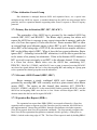
1
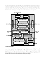
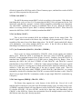
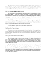
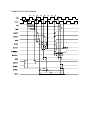
Integrated Circuit Specification
for the
Fat Buster II
Expansion Bus Controller
CSG 4145 - 013
by Dave Haynie
Copyright ©1991 Commodore Technolgy Group
Information contained herein is the unpublished, confidential and
trade secret property of Commodore International Services
Corporation, Technology Group. Use, reproduction or disclosure
of this information without the prior explicit written permission of
Commodore is strictly prohibited.
1.1 General Description
This specification describes the requirements for Fat Buster II, a Bus Controller
Integrated Circuit (I.C.) designed to provide a high speed expansion bus for 68030 based Amiga
computers that meets the specifications for the Zorro III Expansion Bus (see The Zorro III
Expansion Bus Specification for more information on the particular bus protocols described
here).
The Buster chip performs two main functions in an Amiga system. It acts as a bus
protocol converter, translating 68030 cycles into Zorro II or Zorro III cycles, and Zorro II or
Zorro III cycles into 68030 cycles, as appropriate for a particular bus cycle. In addition, it acts as
the bus arbiter for bus requests originating on the Amiga local bus, or on the expansion bus
according to Zorro II or Zorro III protocols. The particular list of features is as follows:
• 68030 to Zorro II cycle conversion with proper synchronization. It supports cache
mapping of Zorro II space, "sloppy cycle" bus snooping, and Zorro II standard bus lock
conversion.
• 68030 to Zorro III cycle conversion, including 68030 burst to Zorro III multiple cycle
translation and quick interrupt cycle types.
• Zorro II and Zorro III to 68030 cycle conversion.
• PIC collision detection for Zorro II and Zorro III.
• Buffer control to support external data and address buffers necessary for Zorro II and
Zorro III bus operation, including a bridging buffer for funneling Zorro II DMA cycles to
either half of a 32-bit 68030 local bus.
• Time-multiplexed bus request for sharing with an alternate high-speed local bus master.
• One local bus 68030-protocol DMA channel.
• Five expansion bus Zorro II/Zorro III protocol DMA channels, with fair arbitration within
channel groups.
• Eight cycle Zorro III scheduling atom with LOCK* override and Zorro III grant timeout.
1.2 Theory Of Operation
A block diagram of the Fat Buster II chip is illustrated below. As mentioned, the
operation of this chip can be cleanly divided into two main groups: bus conversion and bus
arbitration. In the case of bus conversion, there are four types of conversion. The 68030 cycle
may be converted into Zorro II or Zorro III cycles, and the Zorro II or Zorro III cycle may be
converted to a 68030 cycle. The cycle type selector looks at the output of the cycle type selector
to determine which of the conversions to run. The type selector in turn looks at the output of the
primary bus arbiter, to determine the direction of conversion, some Zorro bus and control
information and externally generated chip selects to determine the conversion protocol.
1.2.1 Bus Conversions
As mentioned, the Buster chip supports four types of bus conversions: 68030 to Zorro II,
68030 to Zorro III, Zorro II to 68030, and Zorro III to 68030. In all cases, the Buster chip
provides just the basic logic to perform the conversion. Address mapping and the proper data
buffer arrangement are also very critical to this process. The actual system requirements will
determine the exact details of the external buffer and chip select design.
1.2.1.1 68030 to Zorro II Bus Conversion
The most common conversion mechanism is 68030 to Zorro II bus conversion. This
conversion begins after the address buffers are enabled, 68030 bus is the bus master, AS* is
asserted, WAIT* is negated, and either MEMZ2* or IOZ2* chip selects are asserted to Buster. A
start condition, internally defined based on this and the output of the sloppy cycle snooping logic,
is synchronized by the falling edge of the CDAC clock and the rising edge of the C7M clock, to
create the Zorro II compatible cycle strobe, CCS*. The appropriate data strobes and data buffer
enables follow this according to Zorro II protocols. The DTACK* signal is sampled on the
falling edge of the C7M clock, followed by the rising edge of the CDAC clock, beginning 1.5
C7M cycles after CCS* is asserted. On the next falling edge of C7M after DTACK* is
recognized, the CCS* strobe is negated and the DSACK1* line to the 68030 bus is asserted. If
the 68030 RMC* line is asserted at the end of the a cycle, Buster won’t drop CCS*, but will start
the next cycle, which must be a Zorro II cycle, when called for by the next AS*, keeping CCS*
low through the intercycle time.
Buster also provides DTACK* generation on the expansion bus during Zorro II cycles.
DTACK* is normally driven off the falling edge of the CDAC* clock following the assertion of
CCS*. Assertion of the either the MTCR* line or the CACHE* line from the expansion bus
keeps DTACK* high.
Zorro II support also includes what’s known as sloppy cycle snooping. The Buster device
monitors DTACK*, MTCR*, CACHE*, and the SLAVEN* lines, and will prevent any new cycle
from starting until all of these lines have been negated. This prevents slow Zorro II devices from
interfering with the operation of the next cycle.
1.2.1.2 68030 to Zorro III Bus Conversion
The 68030 to Zorro III conversion begins with the address buffers enabled, the 68030 bus
as bus master. AS* asserted, WAIT* negated, and the ADDRZ3* chip select asserted. The Zorro
III cycle begins with FCS* asserted from the CLK90 rising edge. Address buffer enables are
negated on the next CPUCLK falling edge. Data buffers are enabled on the following CPUCLK
rising edge, and data strobes on the next CLK90 rising edge. After this, DTACK* is sampled on
the rising edge of CLK90, which in turn generates an STERM* for the 68030 bus.
There are two basic variations to this cycle. If the 68030 requests a burst transfer, Buster
will accept an MTACK* request from the Zorro III bus. Upon receipt of this strobe, a burst
transfer will take place. MTCR* is driven for each subcycle, while the low order addresses
A3-A2 are incremented appropriately. The other subcycle type is the interrupt cycle. A 68030
interrupt acknowledge cycle is translated into a Zorro III interrupt acknowledge cycle. On the
second rising edge of CLK90 following the assertion of FCS* and MTCR*, Buster will latch the
state of the SLAVEN* lines and negate MTCR*. If one or more is asserted, a priority encoder
selects one, which indicates which board wins the right to supply the interrupt vector for this
cycle. The MTCR* strobe is again asserted, along with the selected SLAVEN* line and the low
order data strobe. The rest of the cycle concludes as a normal Zorro III cycle.
1.2.1.3 Zorro II to 68030 Bus Conversion
When a Zorro II device has the expansion bus, it may be necessary for Buster to convert
Zorro II cycles into 68030 bus cycles. When a cycle begins that’s not detected as being in Zorro
II space (eg, either MEMZ2* or IOZ2* are asserted), it must be converted to a 68030 cycle. This
is started by sampling CCS* and the data strobes with the CLK90 clock. If its a read cycle,
things can begin based on CCS*, if a write, the cycle on the 68030 bus can’t start until the data
strobes are asserted. Once the appropriate Zorro II signals are latched, the 68030 cycle begins
with AS* and DS* asserted. The A1 line is used to determine which half of the 32-bit bus is of
interest during a read, while both halves are written during a write cycle. The conversion logic
waits for a 68030 bus termination signal, which is assumed to indicate a 32-bit port. If it is in
fact a 32-bit port, this termination becomes DTACK* on the Zorro II bus. If it is actually a
16-bit port and A1 indicates the lower half of the 32-bit bus, extra time is inserted while the "bus
bridge" buffers, carrying expansion data to D15-D0, are turned off and the D31-D16 buffers are
turned on. The cycle is then terminated as for the 32-bit port. This part does not support Zorro II
DMA cycles to an 8-bit 68030 bus port.
1.2.1.4 Zorro III to 68030 Bus Conversion
As with the Zorro II bus masters, a Zorro III bus master is likely to access 68030
resources, so a cycle conversion must be performed. When a cycle begins that’s not detected as
being in Zorro III space (eg, ADDRZ3* is asserted), it must be converted to a 68030 cycle. This
is started by sampling FCS* and then the Zorro III data strobes. It is assumed that, in any system
requiring Zorro III DMA access to 68030 resources, that the external address buffers will latch
DMA addresses on FCS*. Once FCS* and at least one data strobe has been sampled, the 68030
cycle begins with AS* and DS* asserted. Since the Zorro III bus is a fixed-width 32-bit bus,
there’s a direct connection between it and the 68030 bus at this time, and only 32-bit ports on the
68030 bus may be addressed. The asynchronous termination signals are sampled on the falling
edge of CPUCLK, while the synchronous termination signal is sample on the rising edge of
CPUCLK. The output of both samplings is sent to a final stage and gated out to the Zorro III bus
as DTACK* on the next CPUCLK falling edge.
Note that Zorro DMA into 68030 space is the one case in this design where the external
geographic mapping of resources isn’t strict. All Zorro bus cycles are typed by address space
alone. However, DMA onto the 68030 bus is typed according to which of the cycle strobes is
asserted by the bus master. In fact, the same 68030 bus resource can be seen as a 16-bit resource
by a Zorro II master and a 32-bit resource by a Zorro III master.
1.2.2 Bus Arbitration
The bus arbiter section of Buster is completely self-contained. There are two kinds of
expansion bus requests, Zorro II and Zorro III requests. These enter the Buster device on the
EBRN lines. The difference between Zorro II and Zorro III style requests are in the data format;
a Zorro II request asserts EBRN until after a corresponding EBGN is returned, while a Zorro III
request sends a 140ns pulse on EBRN. The first stage of the expansion bus arbiter logically
separates Zorro II from Zorro III requests. Buster also manages requests from the local 68030
bus. These local requests, plus group requests from both Zorro II and Zorro III, are managed by
a subsystem called the primary bus arbiter.
1.2.2.1 Zorro II Arbitration
A Zorro II bus request is handled by the Zorro II slot arbiter subsystem in Buster.
Incoming Zorro II requests are grouped and passed on to the primary arbiter. When the primary
arbiter decides to honor any Zorro II request, it passes a group grant back to the Zorro II arbiter.
Once it receives its group grant, this arbiter selects one grant to pass back to a Zorro II device.
This selection process is based on a priority encoder similar to that used for Zorro II arbitration
in the original Buster for the A2000. One addition is a fairness flip-flop for each channel. This
ensures that once a channel has been granted bus access, it doesn’t get access again until all other
pending requests are serviced. The Zorro II request and grant protocol is directly based on the
68000 bus arbitration protocol.
Original Zorro II bus masters indicated bus ownership by asserting both OWN* and
EBGACK*, with timing designed to minimize the chance of bus contention. Since the Buster
chip now controls the bus buffers in a more complex manner, it uses the presence of either of
these signals to hold the bus for Zorro II. Various Buster details assume that Buster-based
systems will still use OWN* as the basis for address buffer direction control.
1.2.2.2 Zorro III Arbitration
A Zorro III bus request is handled by the Zorro III slot arbiter subsystem in Buster. An
incoming Zorro III request pulse will toggle the state of the registry flip-flop for that channel.
This serves to generate new requests for unregistered channels and to terminate requests for
registered channels. This arbiter groups the set of registered channels into a group request which
is passed to the primary arbiter. When the primary arbiter decides to honor any Zorro III request,
it passes back a group grant to this arbiter.
Zorro III devices follow a request/grant protocol much different than that used in
traditional 680x0 systems. The incoming "request" is really a request for registry. A registered
master will be scheduled for bus cycles as they become available, but there’s no defined
relationship between request for registery and grant. The Zorro III arbiter waits for a defined
arbitration confition before rescheduling a Zorro III master. The first Zorro III master registered
will force the arbitration condition, while subsequent registered masters will be scheduled in at
the next arbitration point. At arbitration time, the arbiter considers all registered masters that
don’t have their fairness flip-flop set. These are each passed through a priority encoder, which
results in the selection of one device to master the bus.
The arbiter next asserts a grant signal to the chosen master. It has a short time (several
microseconds) to master the bus. If the bus isn’t mastered in the given time, a timeout condition
is signalled, causing the grant to be negated and the master unregistered. Assuming the master
takes the bus, it is allocated up to eight full cycles on the bus before the next arbitration
condition. The first cycle run by the master will set its fairness flip-flop to the "used" condition.
Assertion of the LOCK* signal to Buster will prevent rearbitration indefinitely.
Once the current master starts its last cycle, Buster will negate its grant a prepare to
schedule the next master. Assuming there is at least one registered master in the unused state,
the first of those masters will be granted the bus once the current master completes its cycle. If
there are no unused masters left, all the fairness flip-flops are cleared and the arbitration selects
from the full set. Once no devices are registered, the Zorro III arbiter withdraws its group
request from the primary arbiter.
Zorro III masters have no need to deal with the OWN* or EBGACK* signals, so these
are driven by the Buster logic during Zorro III DMA. EBGACK* generally serves no purpose
other than to inform other bus masters that some device other than the default 68030 bus device
is mastering the expansion bus. On the other hand, the OWN* signal is generally used by
external address buffers as a direction indicator.
1.2.2.3 The Primary Arbiter
The Buster device assumes that there is a default bus master on the 68030 bus, as there
always is in the case of a real 68030 system. This master has primary control of the 68030 bus,
and must honor a bus request via BR* before any alternate master can take over. The job of the
primary arbiter is to deal with taking the 68030 bus in response to the various levels of request.
Especially in the case of expansion bus requests, since neither expansion bus protocol has or
should have special knowledge of how the 68030 bus operates.
The primary bus arbiter deals with three main sources of request; the Zorro II group
request, the Zorro III group request, and the 68030-style channel (SBR*/SBG*), in increasing
order of priority. Any of these requests starts up a subsection called the bus request arbiter.
Buster time-multiplexes the external BR* line to allow an alternate 68030 bus master to grab the
bus very quickly, without having to go through the normal Buster priority channeling. Buster
will only sample and drive this lin e on the rising edge of CPUCLK. Its expect that the external
device only sample and drive this line on the falling edge of CPUCLK. In this way, if it detects
BR* negated as CPUCLK rises, Buster asserted BR* and assumes the grant coming back from
the default master is intended for it. If it detects BR* already asserted, Buster waits for BR*
negated before driving it out.
The grant once received, Buster selects between the 68030 channel and the two group
channels, according to the aforementioned priority order. If the 68030 channel wins, Buster
simply echoes the state of BG* onto SBG*, since this device knows the 68030 bus acquisiton
protocol. If the request is instead from either Zorro II or Zorro III groups, the primary arbiter
will master the 68030 bus itself, by asserting BGACK* and negating BR* in response to BG*.
Once BGACK* is properly asserted, it will return a group grant to the winner of the primary
arbitration. The bus grabbing mechanism holds the 68030 bus automatically as long as there’s a
pending grant or a master still granted the expansion bus.
1.3 Pin Configuration
Pin
Name
1
2
3
4
5
6
7
8
9
10
11
12
13
14
15
16
17
18
19
20
FCS*
CCS*
A2
A1
A0
RW
SIZ0
SIZ1
AS*
DS*
DSACK0*
DSACK1*
STERM*
GND
RMC*
SBR*
SBG*
CIIN*
MTACK*
DTACK*
Type
Pin
Name
io
io
io
io
io
io
io
io
io
o
i
io
io
g
io
i
o
io
io
io
21
22
23
24
25
26
27
28
29
30
31
32
33
34
35
36
37
38
39
40
DOE
WAIT*
BR*
BG*
BGACK*
HLT*
BERR*
GND
RESET*
CPUCLK
C7M
CDAC*
D2P*
DBOE1*
DBOE0*
DBR16*
DBLT
READ
EDS2*
EDS3*
Type
io
i
io
o
io
i
o
g
i
i
i
i
o
o
o
o
o
io
io
io
Pin
Name
41
42
43
44
45
46
47
48
49
50
51
52
53
54
55
56
57
58
59
60
61
62
63
64
65
66
67
68
69
70
71
72
73
74
75
76
77
78
79
80
81
82
83
84
LOCK*/EA1
VCC
ABOE2*
ABOE0*
MS2
MTCR*
CINH*
A3
CBREQ*
CBACK*
IOZ2*
MEMZ2*
ADDRZ3*
MS1
OWN*
GND
EBGACK*
CLK90
SLAVE4*
EA2
EA3
EDS0*
EBCLR*
SLAVE3*
SLAVE2*
SLAVE1*
SLAVE0*
BIGZ*
EBG4*
GND
EBG3*
EBG2*
EBG1*
EBG0*
ABOE1*
EBR4*
EBR3*
EBR2*
EBR1*
EBR0*
MS0
BINT*
EDS1*
VCC
Type
io
p
o
o
i
io
io
io
i
o
i
i
i
i
io
g
io
i
io
io
io
io
o
io
io
io
io
o
o
g
o
o
o
o
o
i
i
i
i
i
i
io
io
p
2.0 Signal Description
The various Buster signals are described here, based on their functional categories. For
more details on the 68030 signals, consult The MC68030 User’s Manual, from Motorola. For
more details on the Zorro II-equivalent signals, consult A500/A2000 Technical Reference
Manual, from Commodore-Amiga, and The MC68000 User’s Manual, from Motorola. For more
details on the Zorro III signals, consult The Zorro III Bus Specification, from Commodore.
2.1 Power Group
This section covers signals related to chip power supply. For more information on power
supply in general, see the ratings section of this document.
2.1.1 Power (Vcc)
The Buster chip is supplied by two power pins. It requires these to be at 5V
DC, ±5%, throughout its operating range.
2.1.1 Ground (GND)
The Buster chip’s ground return is on four ground pins.
2.2 Clock Group
The Buster chip’s internal event timing is governed by various clocks, supplied to it by
the system.
2.2.1 High Speed Clocks (CPUCLK, CLK90)
The CPUCLK is the main clock used by Buster for all of its synchronous
event timing. This is the same clock used to drive the 68030 events on the 68030
bus interface. It can be from 16MHz to 25MHz. The CLK90 clock is a secondary
basis clock for Buster. This is essentially the main CPUCLK delayed by at least
10ns from either edge of CPUCLK.
2.2.2 Video-Derived Clocks (C7M, CDAC)
The C7M clock, derived from the 28MHz video basis clock on most Amiga
systems, is the basis clock for Zorro II cycles, which should be between 7.09MHz
and 7.16MHz. This clock is also used as the basis for sampling bus registry pulses
in Zorrro III bus arbitration. The CDAC clock is equivalent to the C7M clock
delayed by 90°. It is used by the Zorro II state logic and as a synchronization clock
for 68030 bus access to Zorro II.
2.3 Chip Select Group
The operation of the Buster chip as a bus cycle converter is triggered mainly by various
chip selects. Buster will stay quiescent until at most one of the three selects has been asserted by
system logic.
2.3.1 Zorro II Memory Select (MEMZ2*)
When the 68030 bus is bus master, MEMZ2* asserted causes Buster to run a
cachable 68030 to Zorro II conversion cycle. During this cycle the CIIN* line on
the 68030 bus will be negated, and all read cycles translate into 16-bit (eg, full
port) reads, to support caching on the 68030 bus. When a Zorro II device is bus
master, MEMZ2* asserted will prevent Buster from performing a Zorro II to 68030
bus conversion.
2.3.2 Zorro II I/O Select (IOZ2*)
When the 68030 bus is bus master, IOZ2* asserted causes Buster to run a
non-cachable 68030 to Zorro II conversion cycle. During this cycle the CIIN* line
on the 68030 bus will be asserted, and all read or write cycles are sized as specified
by the 68030 bus (eg, A1, A0, SIZ1, and SIZ0). When a Zorro II device is bus master, IOZ2*
asserted will prevent Buster from performing a Zorro II to 68030 bus conversion.
2.3.3 Zorro III Select (ADDRZ3*)
When the 68030 bus is bus master, ADDRZ3* asserted causes Buster to run
a 68030 to Zorro III conversion cycle. Caching during Zorro III is of course
achieved by translating the state of the Zorro III CINH* line to the 68030 CIIN*
line. When a Zorro III device is bus master, ADDRZ3* asserted will prevent
Buster from performing a Zorro III to 68030 bus conversion.
2.4 Buffer Control Group
This group is responsible for the control of the data and address bus buffers that sit
between the expansion bus and the 68030 bus.
2.4.1 Address Buffer Enables (ABOEN*)
There are three address buffer control signals: ABOE2*, ABOE1*, and ABOE0*. The
first of these, ABOE2*, is only used during Zorro III cycles. It is asserted to connect A31-A24 of
the 68030 bus to AD31-AD24 of the Zorro III bus. This signal is only active during the address
phase of a 68030 to Zorro III translation, or during the entire cycle for a Zorro III to 68030
translation (the Buster chip expects external logic to properly latch the Zorro III address in this
case).
The next of these strobes, ABOE1*, is asserted to connect A23-A8 of the 68030 bus to
AD23-AD8 of the Zorro III bus. This signal is active during the address phase of a 68030 to
Zorro III translation, or during the entire cycle for a 68030 to Zorro II or any Zorro to 68030
translation. In the case of Zorro III to 68030 translation, the Buster chip expects external logic to
properly latch the Zorro III address such that it’ll remain valid throughout the 68030 cycle.
The final address buffer control strobe is ABOE0*. It is asserted to connect A7-A4 and
any other address-time signals (like the FC2-FC0 lines) between the 68030 and the Zorro bus.
This is active throughout any cycle in which some kind of bus to bus translation is taking place.
2.4.2 Data Buffer Enables (DBOEN*)
The DBOE1* line is active for all 68030 to Zorro transactions. It becomes active at data
time for Zorro III, at approximately state S3 for Zorro II. It intends to bridge 68030 D31-D24 over
to Zorro III AD31-AD24 and 68030 D23-D16 over to Zorro III ED7-ED0. Logically speaking, that
connects the high-order half of the 68030 bus to the high order half of the Zorro III bus. Based
on bus sizing rules for the 68030 bus, this also effectively bridges the correct half of the 68030
bus over to the Zorro II bus. The Buster chip expects that, for reads to the Zorro II bus, data will
be latched externally (see DBLT for more details). This buffer is also active for Zorro III to
68030 conversions, Zorro II to 68030 writes, and Zorro II to 68030 reads with A1 = 0 (see
DBR16 for more information on the bridge function).
The DBOE0* line is asserted at Zorro III data time for 68030 to Zorro III translations and
for Zorro III to 68030 translations. It bridges the low order 68030 data bus, D15-D0, to the low
order Zorro III data bus, AD23-AD8.
2.4.3 Data Bridge Enable (DBR16*)
This line, DBR16*, is used only for Zorro II to 68030 translations. When the 16-bit
Zorro II bus master needs to access the lower half of the 32-bit 68030 bus, this signal is active. It
is intended to drive a buffer bridge between 68030 data bus D15-D0 and the Zorro II data bus
(given by AD31-AD24 and ED7-ED0 in Zorro III terminology). Bridging occurs when A1=1 on
reads, and is always preformed during writes. If a Zorro II device accesses a 16-bit port on the
68030 bus, the size isn’t known until DSACK* time. In these cases, DBR16* may assert and
then be negated, followed by DBOE1* being asserted, as the DSACK* lines indicate a 16-bit
port responding.
2.4.4 Data Buffer Direction (D2P*)
This signal is the direction indicator for any data buffer activity. When asserted, data
flows from Zorro bus to 68030 bus. When negated, data flows from 68030 bus to Zorro bus.
2.4.5 Address Extension Enable (BIGZ*)
This signal is asserted by Buster during a Zorro II to 68030 translation. It indicates to
external logic that a high order address, A31-A24, needs to be provided on the 68030 bus by some
kind of external logic. That address is usually $00.
2.5 68030 Bus Control Group
The signals in this group are the basic 68030 bus control signals. They are driven
according to all 68030 timing rules. Most are bidirectional, being one direction when the 68030
bus is master, and the other when the Buster chip is translating the cycles of a Zorro bus master.
2.5.1 Cycle Strobes (AS*, DS*)
The AS* and DS* strobes define the basic 68030 cycle. When the 68030
bus is master, AS* is driven by the bus master into Buster. All 68030 to Zorro
cycle translations start referenced to AS*. When the Zorro bus is master and
accessing the 68030 bus as its slave, AS* and DS* are driven out by Buster, based
on either FCS* or CCS* and the appropriate EDSN* lines.
2.5.2 Address Bus (A3-A0)
These are the low order 68030 bus address lines. They’re driven by the 68030 bus master
into Buster, for data sizing and to help generate the EA3-EA1 Zorro lines. When the Zorro bus is
master, they’re driven onto the 68030 bus by Buster, based on EA3-EA1.
2.5.3 Data Direction (R/W)
The R/W strobe is driven by the 68030 bus master to indicate the direction of data flow.
Buster translates this pretty much directly into the Zorro bus READ signal. When servicing a
Zorro to 68030 bus translation, Buster drives R/W directly based on the READ signal.
2.5.4 Data Bus Sizing (SIZ1, SIZ0)
These lines, along with A1-A0, determine the transaction size on the 68030 bus. They’re
driven to Buster during a 68030 to Zorro translation, where they influence the state of the
EDS3*-EDS0* lines. When the Zorro bus masters the 68030 bus, these are generated by Buster
based on the state of EDS3-EDS0, to create a proper 68030 cycle. Note that these size bits are
effectively ignored for 68030 bus reads of Zorro II memory space, and that Zorro reads of 68030
space are always requested as full port reads.
2.5.5 Bus Lock (RMC*)
The 68030 bus master asserts RMC* to lock several bus cycles together. When Buster is
translating these cycles to Zorro II, it’ll assume that the RMC* lock was generated by the TAS
instruction, and therefore generate a locked 68000-compatible read-modify-write instruction.
Any other RMC* condition will result in an undefined Zorro II cycle. When the 68030 bus
master is accessing Zorro III space, RMC* is directly translated into LOCK*. When Zorro III
masters the 68030 bus, LOCK* is similarly translated into RMC*.
2.5.6 Cycle Delay (WAIT*)
This is part of the extended 68030 bus definition created for the Amiga 3000. The
WAIT* signal, when asserted to the Buster chip, will hold off the generation of a Zorro cycle
regardless of the state of any of the Buster chip selects. The WAIT* signal can hold off a Buster
cycle indefinitely, even across multiple 68030 bus cycles. It has no effect on Buster when
translating Zorro-mastered cycles to 68030 cycles.
2.5.7 Cycle Termination (DSACK1*, DSACK0*, STERM*)
Zorro cycles are always terminated by DTACK*, while several signals can terminate
68030 cycles. When the 68030 is mastering the Zorro bus, Zorro II DTACK* generates a
DSACK1* on the transition between Zorro II states S6 and S7. Similarly, Zorro III DTACK* is
translated into STERM*, synched up to CLK90 prior to being driven by Buster. Zorro II
mastering the 68030 bus will have STERM* or both DSACK1* and DSACK0* asserted
translated into a Zorro II DTACK*. A DSACK1* alone returned to Buster will create a special
long cycle to adjust for a wrong guess at which read data buffer should be enabled (eg, Buster
assumes a 32-bit port, and will adjust here if the port is actually 16-bits wide). Zorro III
mastering the bus will accept either STERM* or both DSACK1* and DSACK0* as a proper
termination, which will be translated into DTACK* as soon as 68030 bus data is valid. Zorro III
doesn’t accept single DSACK1* termination, neither accepts single DSACK0* termination (eg,
8-bit ports).
2.5.8 Cache Support (CBREQ*, CBACK*, CIIN*)
The Buster chip supports two cache features of the 68030 bus. First of all, it will
translate 68030 cache burst cycles into Zorro III multiple transfer cycles, for either read or write.
A CBREQ* asserted to Buster will cause Buster to snoop for MTACK* during a Zorro III cycle.
If it detects MTACK*, it’ll drive MTCR* on the bus at data time, and immediately return
CBACK* to the 68030 bus. Buster does not translate Zorro III multiple transfer cycles back to
68030 bursts since they don’t directly map back.
The CIIN* signal is asserted to the 68030 bus by Buster during a 68030 master access to
Zorro II I/O space. It is also asserted to the 68030 bus in response to the CINH* line being
asserted during a Zorro III cycle. When a Zorro III master accesses the 68030 bus as a slave, any
assertion of CIIN* will be directly translated to an assertion of CINH* on the Zorro III bus.
2.5.9 Trap Processing (BERR*, RESET*, HLT*)
The Buster chip will assert the BERR* signal onto the 68030 bus when it detects a Zorro
PIC collision during a Zorro cycle. Unlike 16-bit Zorro II systems, collisions between
motherboard space and Zorro space are impossible in this implementation, since the Fat Buster
chip won’t generate Zorro bus cycles for non-Zorro address space. Additionally, any assertion of
the BINT* line on the Zorro bus will result in BERR* on the 68030 bus.
The RESET* input is generated to Buster by the I/O Reset, or equivalent, signal on the
system motherboard. Since all Zorro peripherals are reset to their unconfigured state based on
such a reset signal, Buster is set to its powerup state as well on reset. During reset, all bus
requests are ignored, and both Zorro and 68030 buses are in tri-state.
Currently, the HLT* signal is a no-op from Buster’s point of view.
2.6 Zorro Bus Control Group
This section contains the signals responsible for Zorro II and Zorro III bus control. Many
of these signals face one direction for 68030 to Zorro translation, the other direction for Zorro to
68030 translation. Additionally, some have very different functions under Zorro III than under
Zorro II cycles.
2.6.1 Cycle Strobes (CCS*, FCS*, EDSN*)
The CCS* strobe defines a Zorro II cycle, while the FCS* strobe defines a Zorro III
cycle. CCS*, which corresponds to the Zorro II AS*, is driven synchronous to the C7M clock,
FCS* is driven asynchronous; based on 68030 AS* during a 68030-as-master cycle. When a
Zorro bus card masters the bus, Buster uses the strobe driven to determine the cycle type, along
with the address space accessed.
The EDS3*-EDS0* strobes are data strobes, which indicate the actual data bytes accessed
in a Zorro bus cycle. They’re driven at data time for Zorro III, with at S2 with CCS* during
Zorro II reads, and at S4 during Zorro II writes. Only EDS3* and EDS2* are active during Zorro
II cycles, corresponding to Zorro II signals UDS* and LDS*, respectively. When a Zorro device
is bus master, these strobes determine the bus size information for the 68030 bus and the actual
start of the 68030 bus cycle, since the 68030 cycle can’t start until the size request (state of A1,
A0, SIZ1, and SIZ0) is generated.
2.6.2 Addresses (EA3, EA2, LOCK*/EA1)
Buster generates the low order Zorro bus addresses EA3 and EA2 for all 68030 mastered
cycles. Most of the time, they’re based on 68030 addresses A3 and A2. However, during a
multiple transfer cycle that derives from a 68030 burst, A3 and A2 only define the address during
the first subcycle. After that, counters in Buster increment EA3 and EA2 appropriately. The
LOCK*/EA1 line contains the logical EA1 signal, based on 68030 bus A1, for Zorro II cycles.
The state of EA1 during a Zorro II access to a 68030 bus slave generally determines the bus
bridging function necessary to get the 16-bit transfer on the correct half of the 32-bit 68030 bus.
During Zorro III cycles, this line reflects the logical LOCK* signal, based on the 68030 bus
RMC* line. The LOCK* function issimilarly mapped to RMC* for Zorro III access to a
68030 bus slave.
2.6.3 Memory Space (MS2-MS0)
These lines reflect the current memory space code for any transaction. When the 68030
is bus master, these directly reflect the 68030 function code given by FC2-FC0 on the 68030 bus.
Zorro III cycles are generated for all data spaces, though if a coprocessor space cycle takes place
(code 7), the cycle generated is an interrupt poll cycle. Zorro III devices must generate valid
function codes when they act as bus masters. The Zorro II cycle generator will look to these
during Zorro II I/O cycles. The CIIN* line is only asserted on data space cycles, not address
space cycles. No Zorro II cycles are generated by Buster for coprocessor space. Most Zorro II
devices ignore these lines, and they’re really not technically supported under Zorro II. A Zorro
II bus master may drive them valid during access, or it may leave them alone. To support Zorro
II access to 68030 bus resources, it is recommended that a 1K pulldown be used to terminate
MS1, therefore forcing valid address space for any Zorro II master that doesn’t drive these lines.
2.6.4 State Strobes (READ, DOE, CINH*)
The READ strobe is an indicator of the data transfer direction of a bus cycle. It is driven
by the Buster chip for 68030-mastered cycles, based on the state of the 68030 bus R/W line.
During Zorro bus master cycles, the state of READ is reflected on the 68030 bus R/W line.
The DOE strobe is asserted by the Buster chip during Zorro II cycles, either mastered by
a Zorro II device or the 68030. During 68030-mastered Zorro III cycles, it is also driven by the
Buster chip, though during cycles mastered by a Zorro III device, it is driven by that device.
The CINH* strobe is asserted by a Zorro III slave to indicate that it isn’t cachable. 68030
bus masters see this on CIIN*. During Zorro II cycles, this line performs the OVR* function,
letting the Zorro II device drive DTACK* rather than Buster.
2.6.5 Slave Acknowledge (SLAVEN*)
The PIC addressed by any given Zorro bus cycle indicates it is responding to the bus
address by asserting its private SLAVEN* line. Buster uses this response to determine if any
slave is responding, which is used in some cases to make buffer enable and direction decisions.
As well, if more than one PIC responds, Buster can detect this state, called a PIC collision, and
signal an error before data buffers are enabled and bus contention can start.
During an interrupt acknowledge cycle, multiple PICs may assert their respective
SLAVEN* lines, as a request for use of the interrupt vector currently indicated on the bus. This
polling phase of interrupt acknowledge notes which PICs are requesting the vector rights. This is
followed by a vector phase, in which the Buster chip asserts one SLAVEN* line back to the PIC
that wins the vector arbitration.
2.6.6 Transfer Acknowledge (DTACK*)
All Zorro cycles are terminated either by DTACK*, in the case of a successful cycle, or
BINT*, in the case of an error. Buster will create a no-wait-state Zorro II DTACK*
automatically for any Zorro II cycle, unless otherwise instructed. If a Zorro II slave asserts
CINH* (representing the Zorro II signal "OVR*"), that slave may supply a DTACK* of its own.
If a Zorro II slave asserts MTCR* (representing the Zorro II signal "XRDY"), DTACK*
generation is held off until the line is released. For Zorro III cycles, all slaves are responsible for
generation of DTACK*. A Zorro II DTACK* results in the assertion of DSACK1* on the 68030
bus when the 68030 bus is master, while a Zorro III DTACK* results in the assertion of
STERM* under the same conditions. When a Zorro device is master and addresses the 68030
bus as a slave, any DSACK* or STERM* conditions on the 68030 bus are translated into a
DTACK* appropriate for the Zorro cycle type.
2.6.7 Multiple Transfer Cycle Support (MTCR*, MTACK*)
Fat Buster supports the translation of 68030 burst cycles into Zorro III multiple transfer
cycles. When a burst-compatible Zorro III slave is addressed by the 68030 as bus master, it will
assert the MTACK* line. If the 68030 has indicated it will accept burst transfers via the
CBREQ* line, Buster will assert the 68030 bus CBACK* line to acknowledge the burst, and at
data time assert MTCR*. This first cycle will present EA3 and EA2 equivalent to A3 and A2,
respectively. Additional cycles will increment EA3 and EA2, with the appropriate quadword
wrap, to generate the proper Zorro III static address count. Buster will terminate the transfer if
either MTACK* or CBREQ* are appropriately negated. DTACK* is sampled and STERM*
asserted or negated based on the rising edge of CLK90. Because of the DTACK*
synchronization necessary, the minimum burst cycle from the 68030 viewpoint is two clocks.
MTACK* has no function in Zorro II modes, while MTCR* performs the "XRDY" function,
delaying the automatic generation of Zorro II DTACK* as long as it is asserted.
2.6.8 Bus Error Interrupt (BINT*)
This is the Zorro bus error signal. Buster will assert this line in response to a PIC
collision. Additionally, any Zorro bus assertion of this line will be passed on to the 68030 bus
error signal BERR* by Buster. BERR* generation does not filter back to BINT*.
2.7 Bus Arbitration Control Group
Bus arbitration is managed between 68030 and expansion buses, via a special time
multiplexed fast 68030 bus request, a standard channel on the 68030 bus using normal 68030
protocols, and five expansion channels supporting either Zorro II requests or Zorro III registry
protocols.
2.7.1 Primary Bus Arbitration (BR*, BG*, BGACK*)
The mastership of the 68030 bus is governed by the standard 68030 bus
controls: BR*, BG*, and BGACK*. The Buster chip’s primary bus arbiter will
request the 68030 bus is response to any request stream that it manages, and in the
case of a Zorro bus request, it’ll also take the bus. Buster monitors BR* to allow
an external high speed alternate master to drive BR* as well. Buster samples and
drives BR* on the rising edge of CPUCLK, the external device samples and drives
BR* on the falling edged of BR*. When it loses the bus request arbitration, Buster
ignores BG*. Assuming it wins the BR* arbitration, it will be able to grant the bus
to the winner of its primary bus arbitration. If this is the alternate 68030 channel, a
BG* received is sent out simply as an SBG* to the alternate channel. If the winner
is a Zorro bus device, Buster takes over the 68030 bus, monitoring AS*,
DSACK1*, DSACK0*, STERM*, and BGACK* once a grant is returned, asserting BGACK*
once these bus signals indicate the bus is clear, then negating BR* and sending on a group grant
to the expansion bus channel group that won the arbitration.
2.7.2 Alternate 68030 Channel (SBR*, SBG*)
Buster manages a single, traditional 68030 style channel. A request
generated by asserting SBR* will eventually result in a grant returned when Buster
asserts SBG*. The master on this channel then monitors AS*, DSACK1*,
DSACK0*, STERM*, and BGACK* in the normal 68030 fashion, asserting BGACK* out to the
68030 bus and negating SBR* once the bus is clear. Buster will then negate SBG*, and the
alternate master has the bus until it negates BGACK*.
2.7.3 Expansion Bus Request (EBRN*)
The expansion bus request lines EBR4*-EBR0* are asserted to Buster by a Zorro bus
expansion card to register or request use of the Zorro bus (and, by extension, the 68030 bus in
this implementation). Buster filters all EBRN* through a discriminator circuit that separates
Zorro II bus requests from Zorro III registration commands. The chip currently recognizes the
basic Zorro III bus registration/deregistration command, which is given by a 140ns pulse on
EBRN*, clocked on the rising edge of C7M. The Zorro II bus request is made by holding EBRN*
asserted until Buster returns the corresponding EBGN* and the requesting device properly drives
EBGACK* and OWN*.
2.7.4 Expansion Bus Grant (EBGN*)
The expansion bus grant lines, EBG4*-EBG0*, are asserted in response to a proper
request made on the EBRN* lines. As with requests, grants follow two different protocols. For
Zorro II, a grant is returned to indicate when the PIC may look toward mastering the bus. The
potential master must watch for EBGACK*, OWN*, DTACK*, and CCS* negated, then assert
EBGACK*, then negate EBRN*. The Zorro II device has the bus until it negates EBGACK*.
For Zorro III, a PIC registers with Buster via the EBRN* pulse. It will be granted bus
cycles by Buster, which will assert EBGN* to the PIC. The PIC may run a Zorro III cycle any
time is has EBGN* asserted to it. When Buster decides to schedule a different bus master, it will
negate EBGN* duing an active Zorro III cycle. That device will get off the bus at the end of that
cycle. If it needs more cycles, it can wait to be rescheduled. If not, it can deregister by sending
Buster another EBRN* pulse. This Buster chip schedules masters for eight full cycles on the bus,
but that’s strictly an implementation detail and can change any time in the future. The bus
master may assert the LOCK* signal to prevent from being rescheduled. This is intended to
allow atomic cycles to remain atomic. If a PIC is granted the bus and doesn’t respond
reasonably fast, Buster will deregister it and schedule a different device.
2.7.5 Bus Ownership (EBGACK*, OWN*)
Two signals are used to indicate bus ownership, EBGACK* and OWN*. When a Zorro
II device takes over the bus, it asserts EBGACK* and OWN*. This should be according to Zorro
II rules, but the Fat Buster implementation isn’t sensitive to the timing between the two. The
OWN* signal is responsible for address buffer direction control in both Zorro II and Zorro III
modes. When a Zorro III device takes the bus, the Buster chips drives EBGACK* and OWN*.
The OWN* line is of course responsible for address buffer direction control, while the
EBGACK* line is just driven to give Zorro II devices a consistent view of bus activity.
2.7.6 Bus Request Pending (EBCLR*)
The EBCLR* signal is asserted when an unserviced request is pending. It is mainly used
on the bus as an indicator to Zorro II bus hogs that something else wants the bus (other than the
default 68030 bus master, which is always assumed to want the bus).
3.0 Buster Timing
This section considers the timing of internal and external elements of the Buster II chip.
These timing should confrom to the Zorro III specification, but they are not a substitute for use
by PIC designers.
Below is an illustration detailing the signal types depicted in the timing diagrams to
follow. Signals may be driven or undriven, in a known or unknown state. Buses will typically
be represented as "driven, don’t care" when they are being driven, but the data values are
undetermined or don’t cares, while buses in stable condition are represented by the "Driven,
complex", waveform. The Buster chip does not use internal pullups or pulldowns, but in some
cases signals will be pulled up or down in a system, so the timing shown is based on actual
proper use in a system.
Timing information is a bit harder to represent graphically in a real meaningful way. The
general convention is that a grey horizontal line is used to indicate a reference point to some
clock or signal. Another signal with a specified timing based on this reference point is indicated
by a bracket, as shown. Note that the signal isn’t necessarily derived directly from the reference,
only specificed relative to it. Signals that are asynchronously based off another signal are given
by a directed arrow. Finally, if one signal is repeatedly sampled by another at a given point, that
sampling point is indicated via a vertical directed arrow from that sampling edge.
3.1 68030 To Zorro II Translation