1
User's Guide
SWRU010A – October 2004 – Revised May 2005
TRF4903 With MSP430 Demonstration and Development
Evaluation Kit
This document presents the contents of the TRF4903 demonstration and development
tool kit. The user manual provides information on how to operate the
MSP-TRF4903-DEMO kit and describes its hardware and software. Users should
understand the MSP430F449, TRF6903, and the TRF4903 to obtain the full benefit of
this user manual.
Different topics covered in this manual may require different levels of expertise. The
first two chapters are focused on how the kit operates.
If you want to build your own prototype, review the third chapter on how to load
firmware. The later chapters cover hardware and software topics that may require some
additional expertise.
Other related Texas Instruments information includes the following that may be helpful:
TRF4903 data sheet
SWRS023
TRF6903 data sheet
SWRS022
MSP430F449 data sheet
SLAS344
TRF6903 Design Guide
SWRU009
TRF6901 FAQ
SLAD008
For design and product information related to the TRF6903, MSP430, and similar products,
go to:
http://www.ti.com/ismrf
http://www.msp430.com
PDF documents and zip files may be located on Texas Instruments’ website by typing in the
literature number in the Search text box; for example, typing in SWRS022 will locate the
TRF6903 data sheet.
1
2
3
4
5
6
Contents
TRF4903 Demonstration and Evaluation Kit Overview ................................................................. 2
Demonstrating a Wireless Link............................................................................................. 2
Prototyping .................................................................................................................... 7
PCB Hardware Overview ................................................................................................... 9
Software Overview ......................................................................................................... 14
SCHEMATICS .............................................................................................................. 22
List of Figures
1
2
3
Top-Side, Back-Side of the TRF4903 Demonstration Board .......................................................... 4
JTAG Connector ............................................................................................................. 8
TRF4903 RF Block Diagram ............................................................................................... 9
SWRU010A – October 2004 – Revised May 2005
TRF4903 With MSP430 Demonstration and Development Evaluation Kit
1
www.ti.com
TRF4903 Demonstration and Evaluation Kit Overview
4
5
6
7
8
9
10
11
12
13
14
Block Diagram of the MSP430F44x .....................................................................................
Top-Side Silk Screen ......................................................................................................
Bottom-Side Silk Screen ..................................................................................................
JP1 Pin-Out Configuration ................................................................................................
Game Application FLow Chart – Transmit Mode ......................................................................
Game Application FLow Chart – Receive Mode .......................................................................
Communication Protocol ..................................................................................................
TRF4903 Graphical User Interface for RF Evaluation.................................................................
Schematic (Page 1) ........................................................................................................
Schematic (Page 2) ........................................................................................................
Schematic (Page 3) ........................................................................................................
10
10
11
13
15
16
17
21
22
23
24
List of Tables
1
2
3
4
5
1
4-Bit DIP Switch (SW1) Settings and Transmit Frequencies .......................................................... 5
Bill of Materials ............................................................................................................. 11
Antenna Suppliers .......................................................................................................... 13
6-Byte Transmission Data Packet........................................................................................ 18
TRF4903 Game Application Register Values .......................................................................... 18
TRF4903 Demonstration and Evaluation Kit Overview
This chapter provides an overview of the TRF4903 demonstration and development kit.
1.1
Description
The MSP-TRF4903-DEMO kit is used to demonstrate a unidirectional radio frequency (RF) data link
without the need of an external computer, and for prototyping by downloading new software code to the
MSP430F449 through the JTAG connector. This kit is used to evaluate the Texas Instruments TRF4903, a
single-chip multiband RF transmitter. The schematics and layout of the board can be used as a reference
design if desired, limited by the software system parameters of the demonstration firmware.
1.2
Contents
The TRF4903 demonstration and development kit contains:
• One TRF4903 demonstration board (transmitter)
• One TRF6903 demonstration board (receiver)
• User’s manual (this document)
Software is not included in the kit. Software and hardware documentation related to this kit can be
downloaded at http://www.ti.com/ismrf.
1.3
Equipment Requirement
The following equipment is not included in this kit and is required to operate the MSP-TRF4903-DEMO kit:
• Four AAA batteries
• MSP430 bus expansion cable for the JTAG connector, required only for prototyping purposes.
2
Demonstrating a Wireless Link
This chapter explains how to operate the MSP-TRF4903-DEMO kit to demonstrate a RF bidirectional link.
2
TRF4903 With MSP430 Demonstration and Development Evaluation Kit
SWRU010A – October 2004 – Revised May 2005
www.ti.com
Demonstrating a Wireless Link
2.1
Board Description
The demo kit has two circuit boards. The first circuit board (unit) is the transmitter and consists of a
TRF4903 RF transmitter and a MSP430F449 microcontroller. The second circuit board in the kit is a
receiver and consists of a TRF6903 RF transceiver and a MSP430F449 microcontroller. The TRF6903
board is capable of sending and receiving half-duplex wireless data on the European and North
American/US ISM bands. However, for demo purposes, the TRF6903 board is used as a receiver for the
TRF4903 transmitter.
The microcontroller firmware is configured by default to use the 902-MHz to 928-MHz ISM frequency
band. Additional firmware has been developed to operate the TRF4903 demo kit in the European
868-MHz ISM band.See the Operating the TRF4903 Demo Kit in the 868-MHz EU ISM Band application
note (SWRA047) for further information. The firmware for the 868-MHz EU band can be downloaded from
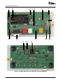
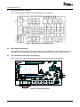
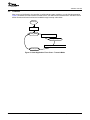
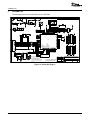
the http://www.ti.com/ismrf website. Figure 1 shows top-side and back-side views of the transmit TRF4903
circuit board.
SWRU010A – October 2004 – Revised May 2005
TRF4903 With MSP430 Demonstration and Development Evaluation Kit
3
www.ti.com
Demonstrating a Wireless Link
a
b
c-1 c-2
d
f
e
k
j
i
l
m
h
g
n
Figure 1. Top-Side, Back-Side of the TRF4903 Demonstration Board
4
TRF4903 With MSP430 Demonstration and Development Evaluation Kit
SWRU010A – October 2004 – Revised May 2005
www.ti.com
Demonstrating a Wireless Link
Circuit board features:
a
On/Off switch
b
Battery holder for two AAA batteries in series (batteries not included).
c-1, c-2
2.2
Headers used to access the MSP430F449 I/O ports.
d
TRF4903 RF transmitter
e
Antenna jumper (0-Ω resistor) used to select either the SMA connector or PCB
antenna (selecting both not recommended).
f
On-board PCB antenna (default configuration). The antenna has modest gain and
radiates in the direction of the bend in the long arm.
g
SMA connector footprint for an external antenna or test equipment (SMA connector
not included).
h
Four-bit DIP switch used in the link demonstration mode to change the transmit/receive frequencies. The switch is connected to MSP430 I/O ports P3.0, P3.1,
P3.2, and P3.3.
i
Four buttons used for the demonstration game application, connected to MSP430
I/O ports P1.0 through P1.3.
j
RS-232C connector
k
JTAG connector
l
TRF4903 I/O header used to monitor or control the TRF4903.
m
Zero-Ω resistor R42, remove to disable the MSP430F449 (or short reset to ground
at JTAG connector).
n
MSP430F449 microcontroller
Operation
A simple game is implemented in the firmware to demonstrate unidirectional RF communication between
the TRF4903 transmit board and the TRF6903 configured in the receive mode. The user starts the game
by pushing any sequence of four colored buttons. The corresponding colored LED’s light up on the receive
board in the same sequence.
• Successful packet reception: The LED’s light up in same sequence as the transmit button sequence.
• Communication error: NO LED’s illuminate on the receiving board if there was a communication error.
2.2.1
Preparing for Operation
Before operating the units as a demonstration, make sure that you have done the following:
• Slide the on/off switch to ON
• Place two AAA batteries on each demonstration board
• Have the same 4-bit DIP switch (SW1) configuration on both boards
Table 1 shows the transmit and receive frequencies selected with the 4-bit DIP switch (SW1). Both circuit
boards must have the same channel switch settings in order for the demonstration game to operate
correctly.
Table 1. 4-Bit DIP Switch (SW1) Settings and Transmit Frequencies
1234 SW1 Setting
(1=On, 0=Off)
TX Frequency (MHz)
4903 TX Board
RX Frequency (MHz)
6903 RX Board
0000
902.3988
891.6992
SWRU010A – October 2004 – Revised May 2005
TRF4903 With MSP430 Demonstration and Development Evaluation Kit
5
www.ti.com
Demonstrating a Wireless Link
Table 1. 4-Bit DIP Switch (SW1) Settings and Transmit Frequencies
(continued)
2.2.2
1234 SW1 Setting
(1=On, 0=Off)
TX Frequency (MHz)
4903 TX Board
RX Frequency (MHz)
6903 RX Board
0001
903.218
892.5184
0010
904.4468
893.7472
0011
905.266
894.5664
0100
906.0852
895.3856
0101
907.7236
897.024
0110
909.362
898.6624
0111
910.1812
899.4816
1000
911.8196
901.12
1001
912.6388
901.9392
1010
913.458
902.7584
1011
914.2772
903.5776
1100
915.506
904.8064
1101
916.3252
905.6256
1110
917.554
906.8544
1111
918.3732
907.6736
Power Up
Slide the power switch to ON. The STANDBY, MODE, and LOCK DETECT LED’s blink to indicate power
up condition. After the power-up initialization, the TRF4903 based transmit unit goes into Standby Mode
(IDLE_STATE) and Mode 0 and waits for a button press. This turns off all the LED’s.
Note:
The LOCK LED on the transmit board is connected to the multiplexed pin 16 of the
TRF4903. Initially, the TRF4903 is programmed to obtain a lock detect signal on the
multiplexed pin 16. This turns on the LOCK DETECT LED on the transmit board.
Once the TRF4903 is ready to transmit data, the multiplexed pin 16 is
programmed for the DCLK mode and the recovered data clock at 38.4 kbps is
output at terminal 16. This blinks the LOCK LED at 38.4 kbps. Once the
transmission is complete, the TRF4903 goes back to Standby (IDLE_STATE)
and the LOCK LED is turned off again.
The TRF6903 based receive board goes into the receive mode to monitor for any transmit activity. The
RSSI indicator LED is lighted to indicate the signal strength in the frequency channel of operation. Red
indicates the lowest signal strength and green indicates the highest.
2.2.3
Wireless Demonstration
Only the TRF4903 transmit board is configured to initiate wireless communication. Assume that Board A is
the transmit board and transmits the first four-button transmitted sequence and Board B receives the
transmission.
Use Board A to start the wireless demonstration by pressing the four colored buttons in any sequence with
about 1/2 second between successive buttons. Once the four buttons are pushed, Board A initiates the
transmission.
Once the transmission is received by Board B and if the response sequence matches, the LEDs are
turned on in the same sequence as the buttons were pushed at the transmitter side.
6
TRF4903 With MSP430 Demonstration and Development Evaluation Kit
SWRU010A – October 2004 – Revised May 2005
www.ti.com
Prototyping
If there are errors due to poor or lost transmission, NO LED lights up on the Board B. This concludes the
basic demonstration of the one-way RF communication.
On completion, the transmit board waits for another button press and the receive board goes back to
receive mode to listen for a new button sequence.
2.2.4
RSSI Indicator
Since the TRF4903 is a transmitter, it does not have an RSSI feature. The TRF6903 receive board is
equipped with a receive signal strength indicator (RSSI) that illustrates the signal strength on the receiver.
Four levels are used to indicate signal strength. Red is the lowest and means no signal was received,
while green indicates the highest level of signal strength. The RSSI shows transmission activity when the
other board is transmitting a data stream on the same DIP switch configuration or when there is another
external RF source broadcasting at that channel frequency. For the best results, the two boards should be
in the same plane of orientation, with the bend in the long antenna arm pointed towards each other.
2.2.5
Error Conditions
Cycle the system power to reinitialize the hardware if you get error conditions that persist. Error conditions
are defined as lost communication, mismatch in response sequences, or response time outs. In some
cases, antenna orientation, signal multipath, or another interfering signal can increase errors.
3
Prototyping
This chapter explains how to operate the MSP-TRF4903-DEMO kit to prototype new applications.
3.1
Connecting to the MSP430 JTAG
The MSP-TRF4903-DEMO is designed for rapid application development. The MSP430 MCU flash
memory can repeatedly be erased and reprogrammed. The on-chip emulation logic allows real-time
debugging and fast code development. The MSP-TRF4903-DEMO and the MSP430 flash emulation tool
provide everything that is required to develop an entire firmware project.
For information go to http://www.msp430.com
Connector J2 provides access to the JTAG port of the MSP430 microcontroller on the
MSP-TRF4903-DEMO circuit board. The MSP-FET430 flash emulation tool (FET) interface board
MSP-FETP430IF (not included in this kit) connects to J2 and allows real-time in-system emulation.
Programming the MSP430, assembler/C source-level debugging, single stepping, multiple hardware
breakpoints, full-speed operation, and peripheral access are fully supported in-system using the JTAG
connector. Figure 2 shows the connections of the MSP-TRF4903-DEMO to the JTAG cable provided by
the MSP430 FET interface board.
SWRU010A – October 2004 – Revised May 2005
TRF4903 With MSP430 Demonstration and Development Evaluation Kit
7
www.ti.com
Prototyping
Keyed
Connector
Red Stripe
Figure 2. JTAG Connector
3.2
Loading the MSP430 With the FIrmware
The MSP-TRF4903-DEMO comes with source code installed on the MSP430 to run the demo program.
The user can develop new application software that can be downloaded to the MSP430 MCU through the
JTAG connector. Since the Compiled C code size is greater than 4 kB, only unrestricted versions of the
IAR development environment (not the Kickstart version) must be used for downloading and modifying the
code.
The workspace file for compiling the demo source code is TRF4903_Demo_US.eww, developed with IAR
compiler version 3.20a.
The following steps show how to open the project file and program the MSP430.
Step 1. Insert the two AAA batteries and slide the on/off switch to ON.
Step 2. Start the Workbench (START->PROGRAMS->IAR SYSTEMS->IAR EMBEDDED
WORKBENCH
Step 3. Use FILE->OPEN WORKSPACE to open the workspace file at: <Installation root>\…\
TRF4903_Demo_US.eww
Step 4. Use PROJECT->BUILD ALL to compile and link the source code. You can view the
source code by double-clicking Common Sources, and then double-clicking on the
source files in the workspace window
Step 5. Ensure that the C-SPY Debugger is properly configured for the Parallel Port used.
(Choose PROJECT->OPTIONS->FET DEBUGGER and select ->LPT1 (default) or LPT2
or LPT3 for the Parralel Port Configuration).
Step 6. Use PROJECT->DEBUG to start C-SPY. C-SPY erases the device Flash and downloads
the application object file
Step 7. In C-SPY, use DEBUG->GO to start the application
Step 8. In C-SPY, use DEBUG->STOP DEBUGGING to exit C-SPY
Step 9. In Workbench, use FILE->EXIT to exit Workbench
8
TRF4903 With MSP430 Demonstration and Development Evaluation Kit
SWRU010A – October 2004 – Revised May 2005
www.ti.com
PCB Hardware Overview
The MSP430 is now programmed with the game demonstration code and ready to operate.
4
PCB Hardware Overview
This chapter provides the default PCB hardware documentation in detail and provides alternate
configurations that the user may want to implement.
4.1
Hardware Overview
The TRF4903 ISM-band transmitter IC operates from 315 MHz to 950 MHz. It has low power consumption
and an operating voltage of 2.2 V to 3.6 V. It features an integer-N PLL synthesizer and supports FSK and
OOK operation. Other features include on-chip clock recovery, brownout detector, and XTAL frequency
trimming in software. See the TRF4903 data sheet (SWRS023) for detailed information on the TRF4903
features.
The TRF4903 demonstration and development kit (MSP-TRF4903-DEMO) provide a stand-alone
demonstration of a unidirectional link using the MSP430F449, the TRF4903 RF transmitter and the
TRF6903 RF transceiver configured as a receiver.
4.2
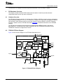
TRF4903 RF Block Diagram
Figure 3 shows the block diagram of the TRF4903 ISM transceiver IC.
16 DET_LD_DCLK
Bit Synchronizer
and
Data Clock
MUX
Band-gap
/ACounter
Brownout
Detector
/N Prescaler
8
24
23
/Div. CTRL
6
Serial
Interface
22
3
2
/BCounter
32/33
CLOCK
DATA
STROBE
STDBY
MODE
Lock
Detect
PA
Output
Divider
1, 2, 3
PFD
CPs
VCO
VCO_TUNE
12
/Ref
2...255
14 CP_OUT
1
XTAL
Switch
19
XTAL_SW
4
XTAL
PA_OUT
TX_DATA
20
Loop Filter
Figure 3. TRF4903 RF Block Diagram
SWRU010A – October 2004 – Revised May 2005
TRF4903 With MSP430 Demonstration and Development Evaluation Kit
9
www.ti.com
PCB Hardware Overview
4.3
MSP430F449 Block Diagram
Figure 4 shows the block diagram of the MSP430F449 microcontroller IC.
Figure 4. Block Diagram of the MSP430F44x
4.4
Demo Board Schematics
See SWRR009 for the TRF4903 transmit side schematics and SWRR001 for the TRF6903 receiver side
schematics. All the schematics for the demonstration boards can be found at http://www.ti.com/ismrf .
4.5
Top and Bottom Silk Screen and Drawing
Figure 5 and Figure 6 show the top-side and bottom-side TRF4903 circuit board silkscreen.
Figure 5. Top-Side Silk Screen
10
TRF4903 With MSP430 Demonstration and Development Evaluation Kit
SWRU010A – October 2004 – Revised May 2005
www.ti.com
PCB Hardware Overview
Figure 6. Bottom-Side Silk Screen
4.6
Parts List
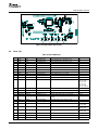
Table 2. Bill of Materials
QTY
VALUE
MFG
MFG NO.
DESCRIPTION
REFERENCE
1
0.5 pF
AVX
06035A0R5CAT2A
CAP, CER, 0603, 50 V, ±0.25 pF, 0.5 pF
C24
1
1.5 pF
AVX
06035A0R5CAT2A
CAP, CER, 0603, 50 V, ±0.25 pF, 1.5 pF
C64
1
22 pF
AVX
06035A220FAT2A
CAP, CER, 0603, 50 V, 1%, 22 pF
C18
1
27 pF
AVX
06035A270FAT2A
CAP, CER, 0603, 50 V, 1%, 27 pF
C17
2
33 pF
AVX
06035A330FAT2A
CAP, CER, 0603, 50 V, 1%, 33 pF
C15, C48
1
43 pF
AVX
06035A430FAT2A
CAP, CER, 0603, 50 V, 1%, 43 pF
C14
1
100 pF
AVX
06035A101FAT2A
CAP, CER, 0603, 50 V, 1%, 100 pF
C54
1
120 pF
AVX
06035A121FAT2A
CAP, CER, 0603, 50 V, 1%, 120 pF
C21
1
75 pF
AVX
06035A820JAT2A
CAP, CER, 0603, 50 V, 5%, 75 pF
C20
1
5600 pF
AVX
06035A562JAT2A
CAP, CER, 0603, 50 V, 5%, 5600 pF
C22
19
0.1 µF
AVX
0603YC104KAT2A
CAP, CER, 0603, 16 V, 10%, 0.1 µF
C23,
C33,
C40,
C45,
C52,
C56,
4
1 µF
AVX
TAJA105K016R
CAP, TANT, 3216, 16 V, 10%, 1 µF
C26, C27, C28, C29
4
22 µF
CAL CHIP
GMC32Y5V226Z16NT
CAP, CER, 1210, 16 V, -20 +80%, 22 µF
C32, C42, C47, C60
3
RED
KingBrite
W934-IT
DIODE, LED, T1, RED, 12.5 MCD at 20 mA
D10, D11, D12
2
MBRM120LT
Motorola
MBRM120LT1 or 3
DIODE, SCHOTTKY, 20PIV, 1A, DO-216AA
D9, D13
3
FMMT2222A
Central Semi
CMPT2222A
XSTR, NPN, GenPurp, 75hfe, 40 Vceo, 600 mA,
SOT23
Q1, Q2, Q3
1
15 nH
Murata
LQW1608A15ND00
IND, SMD, 0603, ±0.5 nH, 650 mA, 15 nH
L6
1
270 nH
Murata
LQW1608A270ND00
IND, SMD, 0603, ±0.5 nH, 650 mA, 270 nH
L5
8
0Ω
AVX
CJ10-000-T
RES, 0603, 5%, 0 Ω
JP1, R6, R29, R31,
R41, R42, R56
6
10 Ω
RES, 0603, 5%, 10 Ω
R35, R38, R39,
R40, R43, R44
6
100 Ω
RES, 0603, 5%, 100 Ω
R45, R46, R47,
R48, R50, R58
3
200 Ω
RES, 0603, 5%, 200 Ω
R61, R62, R63
1
1 kΩ
RES, 0603, 5%, 1 kΩ
R11
1
7.5 kΩ
RES, 0603, 5%, 7.5 kΩ
R9
SWRU010A – October 2004 – Revised May 2005
C30, C31,
C34, C37,
C43, C44,
C46, C51,
C53, C55,
C57, C58, C59
TRF4903 With MSP430 Demonstration and Development Evaluation Kit
11
www.ti.com
PCB Hardware Overview
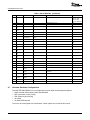
Table 2. Bill of Materials (continued)
QTY
4.7
VALUE
MFG
MFG NO.
DESCRIPTION
REFERENCE
13
10 kΩ
RES, 0603, 5%, 10 kΩ
R13,
R16,
R19,
R57,
1
15 kΩ
RES, 0603, 5%, 15 kΩ
R10
1
82 kΩ
RES, 0603, 5%, 82 kΩ
R30
1
Header 7 x 2
mm
TSW-107-07-T-D
CONN, HDR, P, 14, 7 x 2 x 0.1, TTH
J2
1
Header 7 x 2 x SAMTEC
2 mm
TMM-107-01-T-D-SM
CONN, HDR, P, 14, 7 x 2 x 2 mm, SMT
J5
1
Header 3
MOLEX
22-28-4030
CONN, HDR, P, 3, 3 x 1x 0.1, TTH
JP2
1
CONN DB-9
AMP
745781-4
CONN, PCB, DB9, F, RT
J1
1
SMA EDGE
Johnson
Components
142-0701-801 (-801 = Au
Plate)
CONN, Coax, SMA, Edge, SMT, 0.062 Thk PCB
CO1
1
4 x SPST
CTS
219-4MST
SW, Slide, 4 X SPST, 20 V at 100 mA, SMT, Sealed
SW1
4
PB SPST, NO
OMRON
B3W-4050
SW, PB-SPST, NO, 50 mA, 24 V, TTH
SW2, SW3, SW4,
SW5
1
SS12SDP2
NKK
SS12SDP2
SW, SLIDE SPDT, PCB, 30 V at 0.2 A
SW6
1
12 mm Switch
Cap
OMRON
B32-1320
Cap, SW, 12 mm sq, fits B3W-4050, Orange
See sample
1
12 mm Switch
Cap
OMRON
B32-1330
Cap, SW, 12 mm sq, fits B3W-4050, Yellow
See sample
1
12 mm Switch
Cap
OMRON
B32-1350
Cap, SW, 12 mm sq, fits B3W-4050, Green
See sample
1
12 mm Switch
Cap
OMRON
B32-1380
Cap, SW, 12 mm sq, fits B3W-4050, Red
See sample
1
2468
MemProtectionD
ev
BC2AAAPC
Battery holder, 2 X AAA, PCB Mount
BAT1
1
TP Red
Kobiconn
41-77B4
Test Point, RED, 0.037 TTH
TP2
3
TP Green
Kobiconn
42-23F8
Test Point, GRN, 0.037 TTH
TP1, TP3,TP 5
1
TP White
Kobiconn
33-85B4
Test Point, WHT, 0.037 TTH
TP4
1
TRF4903PW
Texas Instruments
TRF4903PW
IC, RF XMIT, 315-930 MHZ, FQFP48
U1
1
MSP430F449
Texas Instruments
MSP430F449IPZ
IC, MicroP, MixSig, 16-Bit RISC, 32 kb Flash,
FQFP100
U6
0
TPS76330DB
V
Texas Instruments
TPS76330DBVT
IC, PS LDO Regulator, 30 V at 150 mA, SOT32-5
U3
1
MAX3232SOIC16
Texas Instruments
MAX3232CD
IC, RS232 Driver, 2 Driver, 2 Receiver, SOIC16
U4
1
19.6608 MHz
CRYSTEK Corp
017119
XTAL, SMT, 19.6608 MHz, LCC-5X7
Y2
1
32.768 kHz
Seiko
628-SPT1A-0368
XTAL, SMT, 32.768 kHz, CM202
Y4
SAMTEC
R14, R15,
R17, R18,
R20, R53,
R64, R65, R66
Alternate Hardware Configurations
The MSP-TRF4903-DEMO kit is preconfigured to function under the following assumptions:
• North American ISM frequency band, 902-928 MHz
• NRZ (non-return to zero) coding
• FSK (frequency shift keying)
• 38.4 Kbps
• On-board PCB antenna
The kit can be reconfigured to a limited extent. These options are covered in this section.
12
TRF4903 With MSP430 Demonstration and Development Evaluation Kit
SWRU010A – October 2004 – Revised May 2005
www.ti.com
PCB Hardware Overview
4.7.1
European ISM Frequency Band
The European 868-MHz to 870-MHz ISM band is not covered in the preconfigured system, but it can be
modified by changing software variables; download new software configurations through the JTAG
connector. No hardware changes are needed, but the antenna matching is not optimized for this band.
See the Operating the TRF4903 Demo Kit in the 868-MHz EU ISM Band application note (SWRA047) for
further information. The firmware for the 868-MHz EU band can be downloaded from the
http://www.ti.com/ismrf website.
4.7.2
External Antenna
Significant range performance may be achieved when an external antenna is used. The actual
performance improvement will depend on the antenna design and proper impedance matching. A solder
pad for a SMA connector is provided on the circuit board. The antenna can be mounted onto the SMA
connector. Jumper (JP1) setting must be moved to connect the external antenna to the rest of the RF front
end. Shorting pins 2 and 3 of JP1 with a 0-Ω resistor connects the circuit board antenna. To connect an
external antenna, open pins 2 and 3 and short pins 1 and 2 with a 0-Ω resistor. Figure 7 shows the pin-out
configuration at the silk screen. Table 3 lists information for some antenna suppliers. If the PCB antenna is
not used, leave it unconnected, remove the matching components from each end, and substitute one
100-Ω resistor at each end; this will prevent unwanted coupling between the PCB antenna and the RF
signal.
2
3
1
Figure 7. JP1 Pin-Out Configuration
Table 3. Antenna Suppliers
Supplier
4.7.3
Web Site
Part Number
ISM Band
Nearson
www.nearson.com
S467AM-915S
S467AH-868S
US
European
MaxRad
www.maxrad.com
MEXR902SM
US
Mobilemark
www.mobilemark.com
PSWN3-925S
PSTNS-900S
US
European
W. Badland Ltd.
www.badland.co.uk
Various models
US/ European
Radiall/Larsen
www.radialllarsen.com
Various models
SPDA24832
US
European
RS-232C Port
The circuit board is designed for communication to the MSP430 microcontroller through the RS232 serial
port. The UART driver is implemented in firmware and is used in the RF evaluation mode.
4.7.4
On-Board LDO Voltage Regulator
In normal operation, the battery is connected directly to the circuit board power through R31. There is a
footprint for a low dropout (LDO) regulator for cases where a higher-voltage power supply is used instead
of the on-board batteries. To add an LDO regulator, remove R31 and install Texas Instruments regulator
TPS76330DBV at the U3 footprint.
SWRU010A – October 2004 – Revised May 2005
TRF4903 With MSP430 Demonstration and Development Evaluation Kit
13
www.ti.com
Software Overview
4.7.5
High-Frequency Crystal
The board has a footprint for a high-frequency (4 MHz) microprocessor crystal (Y3) as well as the
low-frequency crystal. The factory board configuration uses the 32-kHz watch crystal (Y4). An internal
frequency multiplier generates the 2.4576-MHz system clock.
4.7.6
Discrete LC Filter or SAW Filter
A SAW filter is typically used to band-limit the received RF signal and reduce RF interference outside the
ISM band. The SAW filter from Murata (SAFC915MA70N-TC11) gives a pass band typical of 902 MHz to
928 MHz, while providing about 30-dB attenuation in the stop band. Insertion loss in the pass band is
about 4.5 dB. This causes a corresponding loss in operational range due to signal attenuation. The SAW
filter is not normally installed at the factory in order to maximize range rather than noise immunity.
There are other hardware configurations for attenuating transmitter harmonics and filtering out-of-band
received noise. It is recommended that discrete LC filters be used for this purpose. See the TRF6903
Design Guide (SWRU009) for a detailed discussion on the design of discrete LC filters.
4.7.7
Disabling the MSP430
In normal operation, the MSP430 microprocessor controls the TRF4903 transmitter and the game user
interface. The RF section can also be controlled directly with external computer software. To disable the
microcontroller, either short the MSP430 reset pin (RST) to ground at the JTAG connector (preferred
method), or remove R42, which disables the voltage supply to the MSP430. The TRF4903 can then be
controlled directly through J5, the 14-pin surface-mount header.
4.7.8
Game and RF Operational Modes (Jumper JP2)
The TRF4903 circuit board comes with jumper JP2 set in the position for the game (demonstration link)
mode, where two circuit boards communicate with each other in game mode to demonstrate a wireless
link. In the other jumper position (RF evaluation mode), the TRF4903 is controlled from external software
run on a PC and the commands are passed through the MSP430. This software can be downloaded from
the http://www.ti.com/ismrf website.
5
Software Overview
This chapter describes the link demonstration firmware that has been flashed to the microcontroller and
external control software for RF test and evaluation.
5.1
Software Description
The demonstration software implements a simple one-way game application utilizing a half-duplex
unidirectional wireless link. The transmit board and receive board have different software. The 4903-based
transmit side software routines are discussed in this section. The software was developed using IAR’s
Embedded Workbench, version 3.20a (www.iar.com). The software files are:
• trf4903_demo_us.ewp – Project file
• trf4903_main.c – Main body of the program written in C languge. All subroutines are called from this
program
• rf_reg.c – C file to configure the TRF4903 registers
• api_4903.c – C file for UART interface
• trf4903.s43 – Assembly subroutine to program the TRF4903 registers
• radio49.s43 – Assembly subroutines that execute wireless transmission commands
• setdco.s43 – Assembly routine that sets the baseband clock.
14
TRF4903 With MSP430 Demonstration and Development Evaluation Kit
SWRU010A – October 2004 – Revised May 2005
www.ti.com
Software Overview
5.2
Flowchart
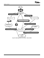
After power up initialization, the controller is configured as a state machine to run the link demonstration.
Figure 8 illustrates the state machine flowchart for the TRF4903 transmit board and the TRF6903 receive
board. Buttons and timer functions are handled through interrupt subroutines.
Power Up
Initialize
IDLE_STATE
Local Button Activated
Local_Button_Active
All 4 Button pushed or 3 sec Timeout
Transmit_Packet
Figure 8. Game Application FLow Chart – Transmit Mode
SWRU010A – October 2004 – Revised May 2005
TRF4903 With MSP430 Demonstration and Development Evaluation Kit
15
www.ti.com
Software Overview
Power Up
Initalize
Receive_Normal
Received Remote Button Packet
Local Button Activated
LED_Remote_Que
Local_Button_Active
Response to Remote Button Complete
Turn on LED
All 4 Button Pushed | 3 sec. Timeout
Wait_For_Local_
Button_Response
Done
Receiver_Wating_For
_Response
Local Button Initiated COM
All Response Button | 3 sec. Timeout
Transmit_Packet
Received Response Packet | 5 Second Timed Out
LED_Response
_Result
Figure 9. Game Application FLow Chart – Receive Mode
16
TRF4903 With MSP430 Demonstration and Development Evaluation Kit
SWRU010A – October 2004 – Revised May 2005
www.ti.com
Software Overview
5.3
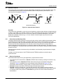
Wireless Protocol
The wireless data communication protocol is digital FSK at 38,400 bits per second with NRZ coding. The
communication protocol used for the demonstration board includes preamble, packet start bit, and
word-sync bit as illustrated in Figure 10.
Packet Start Bit
Pre-Amble
1
0
1
....
1
Bit Width = 26 S
1
1
Word0
0
Word0 Synch Bit
Word1
....
0
....
Word1 Synch Bit
Communication Protocol
Figure 10. Communication Protocol
Preamble
The function of the preamble is to train the receive hardware to set the proper reference voltage threshold
to extract 1 and 0 data. The preamble consists of a train of alternating ones and zeros. A longer preamble
may give better performance at a cost of more time to deliver an equivalent data packet. The current
design has a preamble 100 bits long, or 2.6 ms in duration. Shorter lengths may be used for more
time-critical applications.
5.3.1
Packet Start and Word-Sync Bits
The packet start bit and the word sync bit are used by the receive routine to adjust microprocessor timing
for sampling the incoming data stream. The packet start bit occurs once at the beginning of the data
packet to indicate the end of the preamble and the start of data. The sync bit is used to resynchronize the
bit stream and the data sampling timer. Over time the receive timing could shift in phase relative to
transmit timing due to the small variation in component tolerances and performance. This shows up as an
error in sampled data. The problem gets worse as the packet size increases. Resynchronization minimizes
this drift over time.
Although resynchronization can be done at byte boundaries, word boundary resynchronization is slightly
more efficient.
The data clock recovery feature of the TRF4903 and the TRF6903 provides a convenient way to
synchronize data.
5.3.2
Wireless Data Stream
The wireless data stream for the game application is implemented as follows:
• User initiates an RF transmission on Board A (TRF4903 demo board) by pushing four buttons in any
sequence.
• User sequence is sent to Board B (TRF6903 demo board) using the transmission data packet
described in Table 4, embedded in the communication protocol described in Figure 10. The
transmission packet includes a unique header, four bytes with the button IDs and a checksum.
• Board A then goes to the IDLE_STATE and waits for further button pushes.
• Board B receives the 6 data bytes, calculates the checksum and compares it with the received
checksum. If checksums match, it lights up the LED’s on the receive board in the same order in which
the transmit buttons were pressed. The Board B then goes into the receive mode and listens for
transmissions.
SWRU010A – October 2004 – Revised May 2005
TRF4903 With MSP430 Demonstration and Development Evaluation Kit
17
www.ti.com
Software Overview
Table 4. 6-Byte Transmission Data Packet
5.3.3
Header Byte
Button 1
Button 2
Button 3
Button 4
OxFa
ID Byte
ID Byte
ID BYte
ID BYTe
Checksum Byte
Checksum Byte
Each packet has a checksum byte at the end of the data packet (see Table 4). The checksum byte is
calculated by summing the first 5 bytes of the packet and ignoring overflow.
5.4
TRF4903 Registers
The TRF4903 has five control registers (A through E) that are initialized using an on-chip serial port
interface (SPI). Table 5 shows the values loaded into the registers by the microprocessor during demo
program initialization.
Table 5. TRF4903 Game Application Register Values
Register
5.5
Parameter
Value
A
PA attenuation
Mode 0
Charge Pump
Frequency Band
TX Frequency
0 dB
TX
0.5 mA
915 MHz
902.3488 MHz
B
PA attenuation
PA
Mode 1
Modulation
Brownout threshold
Brownout detector
TX Frequency
0 dB
Enabled
TX
FSK
2.2 V
On
902.3488 MHz
C
Reference divider
Reference frequency
48
409.6 kHz
D
Crystal Tune
Reset Signal for PFD
Crystal Switch during OOK
20.23 pF
Derived From Prescaler
Open
E
Transmit Capture Mode (TXM)
Dividers D1 D2 D3
Terminal 16 Multiplex function
High
38.4 kbps
Lock Detect
Transmit-Side Wireless Subroutines
The game application uses a combination of C and MSP430 assembly language functions to implement
different communication tasks that are required to receive and send data. Brief descriptions of these
subroutines follow.
18
TRF4903 With MSP430 Demonstration and Development Evaluation Kit
SWRU010A – October 2004 – Revised May 2005
www.ti.com
Software Overview
5.5.1
program_TRF4903_word()
This function configures one of the five registers of the TRF4903 transceiver. Here is a sample code on
how to use this function so that you can program all five registers:
struct REGA_BITS{
unsigned long BND:2;
//1-0 Band of operation
unsigned long CP_Acc:2;
//3-2 speed up time for the CP
unsigned long reserved0:1
unsigned long TX:1;
//5
unsigned long PA0:2;
//7-6
unsigned long B_DIV_M0:9; //16-8
Mode 0 = Transmit
unsigned long A_DIV_M0:5; //21-17
unsigned long ADDR:2;
//23-22
};
union TRF_REGA{
unsigned long all;
struct REGA_BITS bit;
};
struct TRF_REG{
union TRF_REGA a;
union TRF_REGB b;
union TRF_REGC c;
union TRF_REGD d;
union TRF_REGE e;
};
void configure_trf4903(void)
{
int pointer;
P4OUT&=0xfe;
pointer=(int)f_sel;
trf4903.a.bit.B_DIV_M0=MAIN_B_T[pointer];
trf4903.a.bit.A_DIV_M0=MAIN_A_T[pointer];
program_TRF4903_word(trf4903.a.all);
trf4903.b.bit.B_DIV_M1=MAIN_B_R[pointer];
trf4903.b.bit.A_DIV_M1=MAIN_A_R[pointer];
program_TRF4903_word(trf4903.b.all);
program_TRF4903_word(trf4903.c.all);
trf4903.d.bit.XTAL_Tune = XTAL_OFFSET;
program_TRF4903_word(trf4903.d.all);
program_TRF4903_word(trf4903.e.all);
5.5.2
send_RF(unsigned int, unsigned int*)
This function is used to transmit a packet of wireless data stream. Here is an example of how it is used:
union RF_XMIT_PACKET{
unsigned int w[MAXWORD];
unsigned char b[MAXBYTE];
}xmit;
void SendRFWithModeSelect(unsigned int ByteCnt)
{
switch(trf4903.e.bit.TXM){
case 0:
send_RF(ByteCnt,xmit.w);
break;
case 1:
trf4903.e.bit.MUX = 1; //set to DCLK mode
program_TRF4903_word(trf4903.e.all);
send_RF_DCLK(ByteCnt,xmit.w);
break;
}
}
SWRU010A – October 2004 – Revised May 2005
TRF4903 With MSP430 Demonstration and Development Evaluation Kit
19
www.ti.com
Software Overview
5.6
External Control Software for RF Evaluation Mode
In the RF evaluation mode, the TRF4903 transmitter is controlled by external software run on a PC rather
than by the game/demo firmware installed on the MSP430. There is no operational link in RF evaluation
mode; the transmitter is set to one operational state at a time. Jumper JP2 sets the board operation mode
to game/demo or RF evaluation.
The RF control software has a graphical user interface (GUI) for the user to set the transmitter frequency,
power, etc. In the RF evaluation mode, the external software GUI controls the TRF4903 by passing control
register words through the computer COM1 serial port, RS232 driver IC (MAX3232), and finally through
the MSP430 microcontroller to the transmitter.
Figure 11 shows the graphical user interface that communicates with the circuit board through the COM1
RS232 serial port. The user must click on the adjacent COM1 button if its caption reads Com1 Closed in
order to open the serial port. The RF evaluation GUI is written in Borland C++ Builder, version 6, and
integrates utilities from Winsoft Ltd. to write to the serial port (Comport). In RF evaluation mode, the serial
port COM1 is used to control the TRF4903.
An example GUI setup for the TRF4903 (transmit mode) is shown in Figure 11. Several boxes and pick
lists have to be filled out by the user before clicking the Send All button to configure the RF transceiver.
Some of the boxes will toggle state when the cursor is placed over the box contents and double-clicked
(power amplifier).
The crystal frequency should be set to 19.6608 MHz. Set the reference divider to 48 (enter value and click
the Set button). The crystal tune capacitance should be set to an intermediate value like 17, 20, or 22 pF.
The charge pump current is 0.5 mA. In the Mode Select box, Either A-Word or B Word can be selected for
transmit mode. The phase-frequency detector reset should be set to Prescaler. Enter the power amp
output frequency and click the Set Freq button; the software rounds off the output frequency to an integer
multiple of the reference frequency. The Band Select List box can be used to select for the ISM band of
operation. The Modulation box should be set to FSK. For initial evaluation, set TXM=0 and TXDATA to
Low. The Multiplex Terminal List box can be used to define the output at terminal 16 of the TRF4903.
Other communication utilities such as HyperTerminal or ProComm can be used in place of the external
software GUI to control the TRF4903 in pass-through mode. Set the transmission raw data rate to
38.4 kbps, 8 bits data, no parity, 1 stop bit, no flow control or handshake. Send the 24-bit control words for
registers A through E in ASCII hex with a leading asterisk (hex 2A) and trailing carriage return (hex 0D),
i.e., “*[A][B][C][D][E]<CR>”.
20
TRF4903 With MSP430 Demonstration and Development Evaluation Kit
SWRU010A – October 2004 – Revised May 2005
www.ti.com
Software Overview
Figure 11. TRF4903 Graphical User Interface for RF Evaluation
5.7
Operation of the TRF4903 Evaluation Kit in the European ISM Band
The European ISM band covers the frequency band from 868 MHz to 870 MHz. A different set of firmware
needs to de downloaded to operate the evaluation kit at the EU band. The firmware can be downloaded
from the www.ti.com/ismrf website. See the Operating the TRF4903 With MSP430 Evaluation Kit in the
868 MHZ European ISM Band application report (SWRA047) for detailed information on the 868-MHz EU
operation Mode.
SWRU010A – October 2004 – Revised May 2005
TRF4903 With MSP430 Demonstration and Development Evaluation Kit
21
www.ti.com
SCHEMATICS
6
SCHEMATICS
The following figures are the schematics for the TRF4903.
B
A
TP1
TP3
TP5
GND
GND
GND
TP_GRN TP_GRN
TP_GRN
C
D
R31
0
VCC
ZONE
ALL
VCC_RF
R56
BAT−SW2
BAT−S W
MBRM120LT3
3
EG1218
2468
C42
+ 22uF
−20+80%
16V
JP2
HEADER 3
U3
1
3
IN OUT 5
EN GND 2
3.0V@150mA
TPS76330DBV
DNP
C32
+ 22uF
−20+80%
16V
VCC
DEMO
4.9152MHZ
C35
10pF
EVK
R30
82K
VCC
4
XTAK2O UT
VCC
32.768KHZ
XTAL1IN
XTAL/TCLK
R29
0
J2
C37
.1uF
.1uF
C33
.1uF
C31
.1uF
C34
.1uF
C30
.1uF
TDO/TDI
TDI
TMS
TCK
P6.5
P6.4
P6LED3
P6LED2
P6LED1
P6LED0
/RST
R42
1
2
3
4
5
6
7
8
9
10
11
12
13
14
HEADER 7X2
VCC
J1
RS232OUT
RS232IN
CONNECTOR DB9
C45
.1uF
C43
.1uF
6
V−
UTXD0
URXD0
T1IN 11
R1OUT 12
T2IN 10
R2OTU 9
VCC 16
C1+ 1
TTL
1
U4
14 T1OUT
13 R1IN
7
8 T2OUT
R2IN
2 V+1
4 C2+
5 C2−
RS232
1
6
2
7
3
8
4
9
5
C1− 3
GND 15
C46 MAX3232−SOIC16
.1uF
A
AVCC 100
DVCC1 1
DVCC2 60
XOUT/TCLK9
XT2IN 89
/RST_NMI 94
TCK 93
TMS 92
TDI 91
TDO/TDI 90
XT2OUT 88
XIN 8
S2
S3
S4
S5
S6
S7
S8
S9
S10
S11
S33
S32
S31
S30
S29
S28
S27
S26
S25
S24
S23
S22
S21
S20
S19
S18
S17
S16
S15
S14
S13
S12
VREF−
R41
0
C47
+ 22uF
−20+80%
16V
P3.2
P5.4
P5.5
P5.7
P5.2
P4.2
P4.4
P4.6
P1.3
P1.1
/RST
P6LED1
P6LED3
P6.5
VREF+
VREF−
P5.0
VCC
IO
VCC
Fsel1
Fsel2
Fsel3
Fsel4
IO
1
3
5
7
9
11
13
15
17
19
21
23
25
27
29
31
33
35
37
39
3
2
4
6
8
10
12
14
16
18
20
22
24
26
28
30
32
34
36
38
40
P3.3
P3.1
R03
P5.6
P5.3
COM0
P4.3
P4.5
P4.7
P1.2
P1.0
P6LED0
P6LED2
P6.4
VeREF+
P5.1
HEADER 20X2
VCC
J4
URXD0
S32
S30
S28
S26
S24
S22
S20
S18
S16
S14
S12
S10
S8
S6
S4
S2
14
15
16
17
18
19
20
21
22
23
10K
RF
S33
S32
S31
S30
S29
S28
S27
S26
S25
S24
S23
S22
S21
S20
S19
S18
S17
S16
S15
S14
S13
S12
45
44
43
42
41
40
39
38
37
36
35
34
33
32
31
30
29
28
27
26
25
24
S2
S3
S4
S5
S6
S7
S8
S9
S10
S11
R53
52 COM0
56 R03
LOCK−DET
P3.3
P3.2
P3.1
R03
TX−D ATA
VCC
J3
U6
64 P3.7
65 P3.6
66 P3.5
67
P3.4
68
P3.3/UCLK0
69
70
P3.2/SOMI0
71
P3.1/SIMO0
P3.0/STE0
COM0
LOCK−DET
R46
R47100
R48100
100
R50
100
VCC
DVSS2 61
99
DVSS1 98
AVSS
VREF− 11 VeREF+
VeREF+ 10
VREF+
VREF+ 7
MSPF449
P1.7/CA1
P1.6/CA0
P1.5/TACLK/ACLK
P1.4/TBCLK/SMCLK
P1.3/TBOUT/SVSOUT
P1.2/TA1
P1.1/TA0/MCLK
P1.0/TA0
TX−DATA
MODE
CLK
STDBY
0
LED4
LED3
LED2
LED1
BUT4
BUT3
BUT2
BUT1
2
R58
R45100
100
72
73
74
75
76
77
78
79
MODE
CLK
STDBY
STROB
DATA
46 P4.7/S34
47 P4.6/S35
48 P4.5/S36
49
50P4.4/S37
51P4.3/S38
62P4.2/S39
63P4.1
P4.0
80
81
82
83
84
85
86
87
RF
P4.7
P4.6
P4.5
P4.4
P4.3
P4.2
59 P5.7/R33
58 P5.6/R23
57 P5.5/R13
55
P5.4/COM3
54
P5.3/COM2
53
12
P5.2/COM1
13
P5.1/S0
P5.0/S1
P1.7
P1.6
P1.5
P1.4
P1.3
P1.2
P1.1
P1.0
P5.7
P5.6
P5.5
P5.4
P5.3
P5.2
P5.1
P5.0
P2.7/ADC12CLK
P2.6/CAOUT
P2.5/URXD0
P2.4/UTXD0
P2.3/TB2
P2.2/TB1
P2.1/TB0
P2.0/TA2
J5
13
14
12
11
9
10
7
8
5
6
3
4
1
2
HDR 7X2X2MM
3
P6.0/A0 95
P6.1/A1 96
P6.2/A2 97
P6.3/A3 2
P6.4/A4 3
P6.5/A5 4
P6.6/A6 5
P6.7/A7/SVSin 6
VCC_CPU
STROB
DATA
APPROVED
RPW
Y4
VCC
VCC_CPU
C57
DATE
7−9−04
C36
10pF
R57
10K
XTAL2IN
1
2
1
2
3
BAT
DESCRIPTION
INITIAL RELEASE
Y3
LDO REGULATOR
D9
SW6
BAT1
2 X AAA + 1
− 2
PCB MT
REV
A
OPTIONAL,DNP
0
4
E
REVISIO NS
TP2
VSS 3.5−6.0 VDC
TP_RED
2
4
6
8
10
12
14
16
18
20
22
24
26
28
30
32
34
36
38
40
2
1
3
5
7
9
11
13
15
17
19
21
23
25
27
29
31
33
35
37
39
UTXD0
S33
S31
S29
S27
S25
S23
S21
S19
S17
S15
S13
S11
S9
S7
S5
S3
HEADER 20X2
1
DATE
DWN
C44
7−6−09
RICH WILLIAMS
NOTES: UNLESS OTHERWISE SPECIFIED.
.1uF 1. INTERPERT DRAWING IAW MIL−STD−100. CHK
2. RESISTANCE VALUES ARE IN OHMS.
XX/XX/
XX
X
3. CAPACITANCE VALUES ARE IN FARADS.
APRVD
EXCEPT AS MAY BE OTHERWISE PROVIDED BY CONTRACT, THIS
4. PARTIAL REFERENCE DESIGNATIONS ARE SHOWN
DRAWING OR SPECIFICATION IS THE PROPRIETARY PROPERTY OF
XX/XX/
XX
X
CNOWIRE TECHNOLOGY INC. IT IS ISSUED IN STRICT CONFIDENCE
FOR COMPLETE DESIGNATION, PREFIX WITH UNIT
AND SHALL NOT BE REPRODUCED OR COPIED OR USED (PARTIALLY OR APRVD
WHOLLY) IN ANY MANNER WITHOUT PRIOR EXPRESS WRITTEN
NUMBER, ASSY. DESIGNATION AND SUBASSEMBLY
XX/XX/
XX
X
AUTHORIZATION OF CNOWIRE TECHNOLOGY INC.
DESIGNATION.
B
C
D
CNOWIRE Technology
1400 Coleman Ave.,Bldg , Santa
G−22 Clara, CA. 95050
Title
TRF4903/MSP4310F437
DEMO
Size
Document Number
Rev
B 100014SCH−01
Date:
Wednesday, March 09, 2005
A
Sheet
1
of
3
E
Figure 12. Schematic (Page 1)
22
TRF4903 With MSP430 Demonstration and Development Evaluation Kit
SWRU010A – October 2004 – Revised May 2005
www.ti.com
SCHEMATICS
B
A
DNP
C
DNP
D8
R21
DNP
R23
LEDRED
LED1
LEDGRN
LED3
100
RED
DNP
LEDORN
LED2
100
DNP
LEDYEL
LED4
ORN
100
VCC
D6
R17
10K
DNP
R27
D7
E
GRN
100
DNP
R22
4
D
DNP
R18
10K
R20
10K
R19
10K
4
D2
SW1
YEL
1
2
3
4
8
7
6
5
Fsel1
Fsel2
Fsel3
Fsel4
4 X SPST
VCC
R13
10k
SW5
1
2
R14
10k
R15
10k
R16
10k
RED BUTTON
3
4
3
BUT1
3
5
PB SPST, NO
SW4
1
2
ORANGE BUTTON
3
4
BUT2
5
PB SPST, NO
SW3
1
2
GREEN BUTTON
3
4
BUT3
5
PB SPST, NO
SW2
1
2
2
YELLOW BUTTON
3
4
2
BUT4
5
PB SPST, NO
+
C26
1.0uF
10%
16V
+
C27
1.0uF
10%
16V
+
1
C28
1.0uF
10%
16V
+
C29
1.0uF
10%
16V
CNOWIRE Technology
1
1400 Coleman Ave.,Bldg G−22
, Sa nta Clara, CA. 95050
Title
EXCEPT AS MAY BE OTHERWISE PROVIDED BY CONTRACT, THIS
DRAWING OR SPECIFICATION IS THE PROPRIETARY PROPERTY OF
CNOWIRE TECHNOLOGY INC. IT IS ISSUED IN STRICT CONFIDENCE
AND SHALL NOT BE REPRODUCED OR COPIED OR USED (PARTIALLY OR
WHOLLY) IN ANY MANNER WITHOUT PRIOR EXPRESS WRITTEN
AUTHORIZATION OF CNOWIRE TECHNOLOGY INC.
A
B
C
D
TRF4903/MSP4310F437
EMOD
Size
Document Number
Rev
B 100014SCH−01
Date:
Wednesday, March 09, 2005
B
Sheet
2
of
3
E
Figure 13. Schematic (Page 2)
SWRU010A – October 2004 – Revised May 2005
TRF4903 With MSP430 Demonstration and Development Evaluation Kit
23
www.ti.com
SCHEMATICS
B
A
C2
C
D
E
DNP
4.7pF
R6
0
4
4
RF7
RF8
CO1
SMA EGDE
JP1
0 ohm
U1
C14
5
7
9
C54
100pF
C15
33pF
PAVCC2
DET_LD_DCLK16
TRF4903PW
PA_GND1
PA_GND2
VCO_GND
XTAL_VCC 17
XTAL 19
LOCK−DET
Y2
19.6608MHZ
XTALVCC
3
C17
27pF
XTALSW 20
TX_DATA
VCO
DNP
XTAL
C18
XTALSW
22pF
1
C25
0.5pF
DNP
PA_VCC
TX−DATA
0.5pF
3
6
8 VCO_PRE
10 VCO_COR
11 VCO_BYPASS
STDBY
MODE
STROBE
CLK
DATA
1K
R12
1K
3
2
22
24
23
L5
270nH
LQW18ANR27G00
1.5pF
C24
PAOUT
15 CP_GND
18 DIG_GND
21 GND
43pF
C64
R11
4
STDBY
MODE
STROB
CLK
DATA
RF3
15nH
13 CP_VCC
2
L6
RF5
12 VCO_TUNE
14 CP_OUT
3
1
ANT LOOP
10
5600pF
7.5K
C51 10
.1uF
C40
.1uF
C56
.1uF
D12
RED
D11
RED
2
LL4148 or TBD
MBRM120LT3
R65
Q1
3
Q2
3
FMMT2222A 10k
TP4
TP_WH
T
EXT−TXDATA
FMMT2222A
1
R64
10k
D13
120pF
R9
R63
200
D10
RED
R66
Q3
3
10k
FMMT2222A
2
R43
200
1
C22
VCC
R62
200
1
C60
22uF
−20+80%
16V
R61
15K
C21
+
.1uF
VCC
2
.1uF
C59 10
XTALVCC
R10
75pF
R44
CPVCC
VCC
2
R40
C23
.1uF
10
C48
33pF
C55
.1uF
VCC_RF
TX−DATA
C52 10
LOCK−DET
CPVCC
10
C53
.1uF
R35
C20
STDBY
MODE
STROB
CLK
DATA
2
R38
CPOUT
VCOVCC
VCOVCC2
R39
VCOTUNE
PAVCC
C58
.1uF
1
1
CNOWIRE Technology
1400 Coleman Ave.,Bldg G−22
, Sa nta Clara, CA. 95050
Title
EXCEPT AS MAY BE OTHERWISE PROVIDED BY CONTRACT, THIS
DRAWING OR SPECIFICATION IS THE PROPRIETARY PROPERTY OF
CNOWIRE TECHNOLOGY INC. IT IS ISSUED IN STRICT CONFIDENCE
AND SHALL NOT BE REPRODUCED OR COPIED OR USED (PARTIALLY OR
WHOLLY) IN ANY MANNER WITHOUT PRIOR EXPRESS WRITTEN
AUTHORIZATION OF CNOWIRE TECHNOLOGY INC.
A
B
C
D
TRF4903/MSP4310F437
EMOD
Size
Document Number
Rev
B 100014SCH−01
Date:
Thursday, October 21, 2004
B
Sheet
3
of
3
E
Figure 14. Schematic (Page 3)
24
TRF4903 With MSP430 Demonstration and Development Evaluation Kit
SWRU010A – October 2004 – Revised May 2005
IMPORTANT NOTICE
Texas Instruments Incorporated and its subsidiaries (TI) reserve the right to make corrections, modifications,
enhancements, improvements, and other changes to its products and services at any time and to discontinue
any product or service without notice. Customers should obtain the latest relevant information before placing
orders and should verify that such information is current and complete. All products are sold subject to TI’s terms
and conditions of sale supplied at the time of order acknowledgment.
TI warrants performance of its hardware products to the specifications applicable at the time of sale in
accordance with TI’s standard warranty. Testing and other quality control techniques are used to the extent TI
deems necessary to support this warranty. Except where mandated by government requirements, testing of all
parameters of each product is not necessarily performed.
TI assumes no liability for applications assistance or customer product design. Customers are responsible for
their products and applications using TI components. To minimize the risks associated with customer products
and applications, customers should provide adequate design and operating safeguards.
TI does not warrant or represent that any license, either express or implied, is granted under any TI patent right,
copyright, mask work right, or other TI intellectual property right relating to any combination, machine, or process
in which TI products or services are used. Information published by TI regarding third-party products or services
does not constitute a license from TI to use such products or services or a warranty or endorsement thereof.
Use of such information may require a license from a third party under the patents or other intellectual property
of the third party, or a license from TI under the patents or other intellectual property of TI.
Reproduction of information in TI data books or data sheets is permissible only if reproduction is without
alteration and is accompanied by all associated warranties, conditions, limitations, and notices. Reproduction
of this information with alteration is an unfair and deceptive business practice. TI is not responsible or liable for
such altered documentation.
Resale of TI products or services with statements different from or beyond the parameters stated by TI for that
product or service voids all express and any implied warranties for the associated TI product or service and
is an unfair and deceptive business practice. TI is not responsible or liable for any such statements.
Following are URLs where you can obtain information on other Texas Instruments products and application
solutions:
Products
Applications
Amplifiers
amplifier.ti.com
Audio
www.ti.com/audio
Data Converters
dataconverter.ti.com
Automotive
www.ti.com/automotive
DSP
dsp.ti.com
Broadband
www.ti.com/broadband
Interface
interface.ti.com
Digital Control
www.ti.com/digitalcontrol
Logic
logic.ti.com
Military
www.ti.com/military
Power Mgmt
power.ti.com
Optical Networking
www.ti.com/opticalnetwork
Microcontrollers
microcontroller.ti.com
Security
www.ti.com/security
Telephony
www.ti.com/telephony
Video & Imaging
www.ti.com/video
Wireless
www.ti.com/wireless
Mailing Address:
Texas Instruments
Post Office Box 655303 Dallas, Texas 75265
Copyright 2005, Texas Instruments Incorporated