1
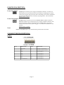
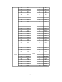
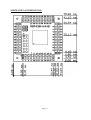
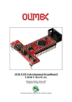
MSP430-H449 development board
Users Manual
All boards produced by Olimex are ROHS compliant
Rev. Initial, June 2011
Copyright(c) 2011, OLIMEX Ltd, All rights reserved
Page 1
INTRODUCTION:
MSP430-H449 is header board for the MSP430F449 mixed signal microcontroller
produced by Texas Instruments.
MSP430-H449 has JTAG port for programming and debugging and most of the
GPIOs are on extension headers where you can connect your additional circuits.
BOARD FEATURES:
-
Microcontroller: MSP430F449 with 60K Bytes Program Flash, 256 Bytes data
Flash, 2K Bytes RAM
-
JTAG connector
-
JTAG Power_In and Power_Out jumpers
-
32 768 Hz oscillator crystal
-
8Mhz crystall oscillator (works only when power supply +3.6V)
-
TEST pin pull-down
-
RST/NMI pin pull-up
-
power supply filtering capacitor
-
extension headers for each uC pin
-
PCB: FR-4, 1.5 mm (0,062"), green soldermask, white silkscreen component print
-
Dimensions: 45x45 mm (1.8x1.8")
-
space between the pin rows: 43.18 mm (1.7")
ELECTROSTATIC WARNING:
The MSP430-H449 board is shipped in protective anti-static packaging. The board
must not be subject to high electrostatic potentials. General practice for working
with static sensitive devices should be applied when working with this board.
BOARD USE REQUIREMENTS:
Cables: The cable you will need depends on the programmer/debugger you use. If
you use MSP430-JTAG, you will need LPT cable, if you use MSP430-JTAG-TINY,
MSP-JTAG-TINY-V2, or MSP-JTAG-ISO, you will need 1.8m A-B USB cable, if you
use MSP430-JTAG-RF, you can connect it to the USB port of your computer, or via
USB cable type A – female.
Hardware: Programmer/Debugger – one of our Programmers – MSP430-JTAG,
MSP430-JTAG-TINY, MSP430-JTAG-ISO, or MSP430-JTAG-RF.
Software: MSP430 KickStart software.
Page 2
PROCESSOR FEATURES:
MSP430-H449 board use MSP430F449 mixed signal microcontroller with these
features:
–
Low Supply-Voltage Range, 1.8 V to 3.6 V
–
Ultralow-Power Consumption:
–
Active Mode: 280 μA at 1 MHz, 2.2 V
–
Standby Mode: 1.1 μA
–
Off Mode (RAM Retention): 0.1 μA
–
Five Power Saving Modes
–
Wake-Up From Standby Mode in 6 μs
–
16-Bit RISC Architecture, 125-ns Instruction Cycle Time
–
12-Bit A/D Converter With Internal Reference, Sample-and-Hold and Autoscan
Feature
–
16-Bit Timer With Seven Capture/Compare-With-Shadow Registers, Timer_B
–
16-Bit Timer With Three Capture/Compare Registers, Timer_A
–
On-Chip Comparator
–
Serial Communication Interface (USART), Select Asynchronous UART or
Synchronous SPI by Software; Two USARTs (USART0, USART1)
–
Brownout Detector
–
Supply Voltage Supervisor/Monitor With Programmable Level Detection
–
Serial Onboard Programming, No External Programming Voltage Needed
Programmable Code Protection by Security Fuse
–
Integrated LCD Driver for Up to 160 Segments
–
60KB+256B Flash Memory
–
2KB RAM
Page 3
BLOCK DIAGRAM:
Page 4
MEMORY ORGANIZATION:
Page 5
CON7
P_IN
1
2
12
11
10
9
8
7
6
5
4
3
2
1
12
11
10
9
8
7
6
5
4
3
2
1
CON8
SCHEMATIC:
P_OUT
1
2
2
4
6
8
10
12
14
100n
100n
25
Q1
32768Hz
Q2
NA
DVCC1
P6.3/A3
P6.4/A4
P6.5/A5
P6.6/A6
P6.7/A7/SVSIN
VREF+
XIN
XOUT/TCLK
VEREF+
VREF-/VEREFP5.1/S0
P5.0/S1
S2
S3
S4
S5
S6
S7
S8
S9
S10
S11
S12
S13
U1
MSP430F449
75
74
73
72
71
70
69
68
67
66
65
64
63
62
61
60
59
58
57
56
55
54
53
52
51
P2.4/UTXD0
P2.5/URXD0
P2.6/CAOUT
P2.7/ADC12CLK
P3.0/STE0
P3.1/SIMO0
P3.2/SOMI0
P3.3/UCLK0
P3.4/TB3
P3.5/TB4
P3.6/TB5
P3.7/TB6
P4.0/UTXD1
P4.1/URXD1
DVSS2
DVCC2
P5.7/R33
P5.6/R23
P5.5/R13
R03
P5.4/COM3
P5.3/COM2
P5.2/COM1
COM0
P4.2
26
27
28
29
30
31
32
33
34
35
36
37
38
39
40
41
42
43
44
45
46
47
48
49
50
C5
C6
NA
50
NA
MSP430-H449
Rev. Initial
COPYRIGHT(C) 2006, OLIMEX Ltd.
http://www.olimex.com/dev
Page 6
CON4
1
2
3
4
5
6
7
8
9
10
11
12
GND
CON3
CON2
1
2
3
4
5
6
7
8
9
10
11
12
13
14
15
16
17
18
19
20
21
22
23
24
25
C8
39pF
1 T DO/T DI
T DI
3
TMS
5
T CK
7
9
RST
11
13
GND
CON5
AVCC
DVSS1
AVSS
P6.2/A2
P6.1/A1
P6.0/A0
RST/NMI
TCK
TMS
TDI
TDO/TDI
XT2IN
XT2OUT
P1.0/TA0
P1.1/TA0/MCLK
P1.2/TA1
P1.3/TBOUTH/SVSOUT
P1.4/TBCLK/SMCLK
P1.5/TACLK/ACLK
P1.6/CA0
P1.7/CA1
P2.0
P2.1
P2.2
P2.3
DVCC
CON1
1
2
3
4
5
6
7
8
9
10
11
12
Q3
8MHz
S14
S15
S16
S17
S18
S19
S20
S21
S22
S23
S24
S25
S26
S27
S28
S29
S30
S31
S32
S33
P4.7/S34
P4.6/S35
P4.5/S36
P4.4/S37
P4.3/S38
GND
1
2
3
4
5
6
7
8
9
10
11
12
C7
39pF
100
99
98
97
96
95
94
93
92
91
90
89
88
87
86
85
84
83
82
81
80
79
78
77
76
C3
1
2
3
4
5
6
7
8
9
10
11
12
100n
C2
DVCC
GND
GND
DVCC
RST
TCK
TMS
TDI
TDO/TDI
100
C1
DVCC
JTAG
75
12
11
10
9
8
7
6
5
4
3
2
1
CON6
12
11
10
9
8
7
6
5
4
3
2
1
R1
47K
C4
10n
GND
BOARD LAYOUT:
POWER SUPPLY CIRCUIT:
MSP430-H449 can take power from two sources:
–
JTAG, when P_IN jumper is closed.
–
EXT connectors, when P_OUT jumper is closed.
RESET CIRCUIT:
MSP430-H449 reset circuit includes R1 (47kΩ), C4 (10nF), JTAG connector pin 11,
CON7 pin 10 and MSP430F449 pin 94.
CLOCK CIRCUIT:
Quartz crystal 32768 MHz is connected to MSP430F449 pin 8 (XIN) and pin 9
(XOUT/TCLK).
Quartz crystal 8 MHz is connected to MSP430F449 pin 88 (XT2OUT) and pin 89
(XT2IN).
Page 7
JUMPER DESCRIPTION:
Power In jumper:
P_IN jumper connects power supply from JTAG connector. You have to
ensure that your circuit doesn't draw more than few milliamperes current
or the power supply may decrease due to the JTAG port current limitations.
P_IN is useful and must be used mostly to program the microcontroller.
Default state is closed.
Power Out jumper:
P_OUT jumper connects power from MSP430-H449 to JTAG connector.
When this jumper cap is placed, the power supply of JTAG connector will
follow the power supply of the board. This is useful when your board
works at lower than +3,3V power supply, or consume more than few mA
current.
Default state is opened.
Note:
P_IN and P_OUT jumper caps should not be placed at the same time.
CONNECTOR DESCRIPTIONS:
JTAG:
Pin #
Signal Name
Pin #
Signal Name
1
TDO/TDI
2
Via jmp V_IN to DVCC
3
TDI
4
Via jmp V_OUT to DVCC
5
TMS
6
Not Connected
7
TCK
8
Not Connected
9
GND
10
Not Connected
11
RST
12
Not Connected
13
Not Connected
14
Not Connected
Page 8
Extension connectors:
CON
CON1
Pin #
Signal
Name
1
CON
Pin #
Signal
Name
DVCC
2
P6.3
3
P6.4
4
P6.5
5
P6.6
6
P6.7
7
VREF+
8
XIN
9
XOUT
10
VEREF+
12
P5.1
CON2
11
VREF-
13
P5.0
14
S2
15
S3
16
S4
17
S5
18
S6
19
S7
20
S8
21
S9
22
S10
23
S11
24
S12
25
S13
26
S14
27
S15
28
S16
29
S17
30
S18
31
S19
32
S20
Page 9
CON4
CON6
CON8
33
S21
34
S22
35
S23
36
S24
37
S25
38
S26
39
S27
40
S28
41
S29
42
S30
43
S31
44
S32
45
S33
46
P4.7
47
P4.6
48
P4.5
49
P4.4
50
P4.3
51
P4.2
52
COM0
53
P5.2
54
P5.3
55
P5.4
56
R03
57
P5.5
58
P5.6
59
P5.7
60
DVCC
61
GND
62
P4.1
63
P4.0
64
P3.7
65
P3.6
66
P3.5
67
P3.4
68
P3.3
69
P3.2
70
P3.1
71
P3.0
72
P2.7
73
P2.6
74
P2.5
75
P2.4
76
P2.3
77
P2.2
78
P2.1
79
P2.0
80
P1.7
81
P1.6
82
P1.5
83
P1.4
84
P1.3
85
P1.2
86
P1.1
87
P1.0
88
XT2OUT
89
XT2IN
90
TDO/TDI
91
TDI
92
TMS
93
TCK
94
RST
95
P6.0
96
P6.1
97
P6.2
98
GND
99
GND
100
DVCC
CON3
CON5
CON7
Page 10
MECHANICAL DIMENSIONS:
Page 11
AVAILABLE DEMO SOFTWARE:
–
Not available
Page 12
ORDER CODE:
MSP430-H449 – assembled and tested
How to order?
You can order to us directly or by any of our distributors.
Check our web www.olimex.com/dev for more info.
Revision history:
Board's revision:
Rev. Initial - January 2006
Manual's revision:
Rev. Initial – June 2011
Page 13
Disclaimer:
© 2011 Olimex Ltd. All rights reserved. Olimex®, logo and combinations thereof, are registered trademarks of
Olimex Ltd. Other terms and product names may be trademarks of others.
The information in this document is provided in connection with Olimex products. No license, express or implied
or otherwise, to any intellectual property right is granted by this document or in connection with the sale of
Olimex products.
Neither the whole nor any part of the information contained in or the product described in this document may be
adapted or reproduced in any material from except with the prior written permission of the copyright holder.
The product described in this document is subject to continuous development and improvements. All particulars
of the product and its use contained in this document are given by OLIMEX in good faith. However all warranties
implied or expressed including but not limited to implied warranties of merchantability or fitness for purpose are
excluded.
This document is intended only to assist the reader in the use of the product. OLIMEX Ltd. shall not be liable for
any loss or damage arising from the use of any information in this document or any error or omission in such
information or any incorrect use of the product.
Page 14