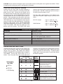
1
LOGIC PROBE KIT
MODEL LP-525K
Assembly and Instruction Manual
Elenco™ Electronics, Inc.
Copyright © 1992 Elenco™ Electronics, Inc.
REV-F Revised 2003
753241
PARTS LIST
If you are a student, and any parts are missing or damaged, please see instructor or bookstore.
If you purchased this LP-525K Logic Probe kit from a distributor, catalog, etc., please contact Elenco™
Electronics (address/phone/e-mail is at the back of this manual) for additional assistance, if needed.
RESISTORS
Qty.
3
1
1
1
1
1
2
2
7
1
1
3
Symbol
R21, R23, R24
R16
R4
R14
R11
R13
R10, R15
R12, R22
R1, R5 - R8, R19, R20
R17
R18
R2, R3, R9
Description
200W 5% 1/4W
2kW 5% 1/4W
4.7kW 5% 1/4W
5.1kW 5% 1/4W
15kW 5% 1/4W
18kW 5% 1/4W
20kW 5% 1/4W
30kW 5% 1/4W
100kW 5% 1/4W
120kW 5% 1/4W
150kW 5% 1/4W
4.7MW 5% 1/4W
Color Code
red-black-brown-gold
red-black-red-gold
yellow-violet-red-gold
green-brown-red-gold
brown-green-orange-gold
brown-gray-orange-gold
red-black-orange-gold
orange-black-orange-gold
brown-black-yellow-gold
brown-red-yellow-gold
brown-green-yellow-gold
yellow-violet-green-gold
Part #
132000
142000
144700
145100
151500
151800
152000
153000
161000
161200
161500
174700
CAPACITORS
Qty.
1
1
2
Symbol
C2
C3
C1, C6
Description
100pF (101) Discap
200pF (201) Discap
.001mF (102) Discap
Qty.
1
1
1
Part #
221017
222010
231036
Symbol
C4
C5
C7
Description
.005mF (502) Discap
.047mF (473) Discap
.1mF (104) Discap
Part #
235018
244780
251010
Description
2N3906 Transistor
LM2901 IC
LED
Part #
323906
332901
350001
SEMICONDUCTORS
Qty.
1
5
2
Symbol
D6
D1 - D5
Q2, Q4
Description
1N4002 Diode
1N4148 Diode
2N3904 Transistor
Qty.
3
1
3
Part #
314002
314148
323904
Symbol
Q1, 3, 5
U1
L1 - L3
MISCELLANEOUS
Qty.
1
2
1
1
2
1
1
1
Description
PC Board
Switch SPDT
Probe Tip
Case
Screw #4 x 5/8”
IC Socket 14-pin
Alligator Clip Black
Alligator Clip Red
Qty.
1
1
1
3’
3”
1”
1
Part #
517014
541024
616001
623005
643450
664014
680001
680002
Description
Label Front
Label Back
Wire 1.5”
Wire 2 cond.
Tubing #20
Shrink Tubing (red)
Solder Tube
Part #
724002
724003
814220
870500
890020
890312
9ST4
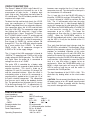
PARTS IDENTIFICATION
Resistor
Diode
Integrated Circuit
Capacitor
Transistor
IC Socket
LED
Switch
-1-
Case Top
Probe Tip
Case Bottom
Alligator Clip
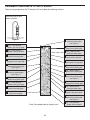
IDENTIFYING RESISTOR VALUES
Use the following information as a guide in properly identifying the value of resistors.
BAND 1
1st Digit
Color
Black
Brown
Red
Orange
Yellow
Green
Blue
Violet
Gray
White
Multiplier
BAND 2
2nd Digit
Digit
0
1
2
3
4
5
6
7
8
9
Color
Black
Brown
Red
Orange
Yellow
Green
Blue
Violet
Gray
White
Resistance
Tolerance
Color
Multiplier
Black
1
Brown
10
Red
100
Orange
1,000
Yellow
10,000
Green
100,000
Blue
1,000,000
Silver
0.01
Gold
0.1
Digit
0
1
2
3
4
5
6
7
8
9
Color
Silver
Gold
Brown
Red
Orange
Green
Blue
Violet
Tolerance
+10%
+5%
+1%
+2%
+3%
+.5%
+.25%
+.1%
BANDS
1
2
Multiplier
Tolerance
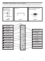
IDENTIFYING CAPACITOR VALUES
Capacitors will be identified by their capacitance value in pF (picofarads), nF (nanofarads), or mF (microfarads). Most
capacitors will have their actual value printed on them. Some capacitors may have their value printed in the following
manner. The maximum operating voltage may also be printed on the capacitor.
Multiplier
For the No.
0
1
2
3
Multiply By
1
10
100
1k
4
5
8
10k 100k .01
9
0.1
Note: The letter “R” may be used at times
to signify a decimal point; as in 3R3 = 3.3
10mF 16V
First Digit
Second Digit
Multiplier
103K
Tolerance
100V
The letter M indicates a tolerance of +20%
The letter K indicates a tolerance of +10%
The letter J indicates a tolerance of +5%
Maximum Working Voltage
The value is 10 x 1,000 = 10,000pF or .01mF 100V
METRIC UNITS AND CONVERSIONS
Abbreviation
p
n
m
m
–
k
M
Means
Pico
nano
micro
milli
unit
kilo
mega
Multiply Unit By
.000000000001
.000000001
.000001
.001
1
1,000
1,000,000
Or
10-12
10-9
10-6
10-3
100
103
106
1. 1,000 pico units = 1 nano unit
2. 1,000 nano units = 1 micro unit
3. 1,000 micro units = 1 milli unit
-2-
4. 1,000 milli units
= 1 unit
5. 1,000 units
= 1 kilo unit
6. 1,000 kilo units
= 1 mega unit
CIRCUIT DESCRIPTION
The Elenco™ Model LP-525K Logic Probe kit is a
convenient and precise instrument for use in the
measurement of logic circuits. It displays logic
levels (high or low), and voltage transients down to
25 nanoseconds. The LED readouts provide instant
response to the logic state.
becomes more negative than the (+) input and the
comparator turns off. The short pulse on the input is
thus stretched to 1.5 milliseconds.
The (–) input (pin 8) of the PULSE LED driver is
biased to +2.5VDC by resistors R19 and R20. The
(+) input is biased to +3VDC by resistors R6 and
R18. The 1.5 milliseconds pulse from the pulse
stretcher grounds the (+) input through diode D5
turning the comparator on and lighting the PULSE
LED. When the PULSE-MEM switch is in MEM, Q5
is also turned on, causing the (–) input of the
comparator to go to +5VDC. This keeps the
comparator on even after the (+) input returns to
+3VDC. When the PULSE-MEM switch is in
PULSE, the feedback path to the (–) input is broken
and the LED is lit only for the duration of the 1.5
milliseconds pulse.
To detect the high and low logic levels, the LP-525
uses two comparators of a Quad Comparator
LM2901 Integrated Circuit (see schematic diagram).
One comparator drives the HI LED and the other
drives the LOW LED. The comparator output goes
low, lighting the LED, when the (–) input is more
positive than the (+) input. To measure TTL circuits,
the TTL-CMOS switch is set to TTL and the red and
black alligator clips are connected to +5VDC and
ground. The (+) input (pin 5) of the HI comparator is
then biased to 2.3VDC by resistor network R9
through R15. Thus, the LED lights when the probe
tip is more positive than 2.3VDC. To measure
CMOS circuits, the HI comparator changes to
3.5VDC or 70% of the supply voltage.
Thus, each time the input signal changes state, the
PULSE LED is activated for 1.5 milliseconds. When
observing low frequency signals, the PULSE LED
provides an immediate indication of this pulse
activity. By observing the HI and LOW LEDs, the
polarity of the pulse train can be determined. Low
frequencies cause the PULSE LED to blink once for
each transition. High frequencies cause the LED to
flash at a rate that makes it appear to be on
continuously. When the PULSE-MEM switch is in
MEM, a single input pulse will cause the PULSE
LED to come on and stay on until the switch is
returned to the PULSE position.
The (–) input of the LOW comparator is biased to
.8VDC for TTL operation and 1.5VDC or 30% of the
supply voltage for CMOS operation. The LOW LED
thus lights when the probe tip is connected to
voltages less than .8 or 1.5VDC.
The pulse LED is controlled by a bipolar edge
detector circuit which responds to both positive and
negative transients. This circuit is made up of
capacitors C2 and C3, transistors Q1 through Q4,
and the associated resistors. When the circuit is
activated by pulses as short as 25 nanoseconds, a
negative pulse is applied to the (+) input (pin 11) of
the pulse stretcher comparator. The comparator
then turns on and is held by the feedback resistor
R8. The ground level on the output (pin 13) causes
C5 to discharge through R17. In approximately 1.5
milliseconds, the voltage on the (–) input (pin 10)
The input impedance of the LP-525 is 1MW. This
eliminates any loading effect on the circuit under
test.
CAUTION: Do not connect the alligator clips to any
AC power source or to a DC power source greater
than 35VDC. Failure to comply with this warning
may result in damage to this instrument.
SPECIFICATIONS
Input Impedance
Input Overload Protection
Thresholds
TTL
CMOS
Response better than
Pulse Detector
Power Requirements
Operating Temperature
1MW
50V DC continuous
Logic 1
Logic 0
2.3 + .25V
0.80V + .1V
70% Vcc
30% Vcc
25 nanoseconds
1.5 millisecond pulse stretcher
5V Vcc @ 30mA
15V Vcc @ 40mA
–40OC to +85OC
-3-
CONSTRUCTION
Introduction
The most important factor in assembling your LP-525K Logic Probe Kit is good soldering techniques. Using the
proper soldering iron is of prime importance. A small pencil type soldering iron of 25 - 40 watts is
recommended. The tip of the iron must be kept clean at all times and well tinned.
Safety Procedures
• Wear eye protection when soldering.
• Locate soldering iron in an area where you do not have to go around it or reach over it.
• Do not hold solder in your mouth. Solder contains lead and is a toxic substance. Wash your hands
thoroughly after handling solder.
• Be sure that there is adequate ventilation present.
Assemble Components
In all of the following assembly steps, the components must be installed on the top side of the PC board unless
otherwise indicated. The top legend shows where each component goes. The leads pass through the
corresponding holes in the board and are soldered on the foil side.
Use only rosin core solder of 63/37 alloy.
DO NOT USE ACID CORE SOLDER!
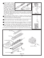
What Good Soldering Looks Like
Types of Poor Soldering Connections
A good solder connection should be bright, shiny,
smooth, and uniformly flowed over all surfaces.
1.
Solder all components from
the copper foil side only.
Push the soldering iron tip
against both the lead and
the circuit board foil.
1. Insufficient heat - the
solder will not flow onto the
lead as shown.
Soldering Iron
Component Lead
Foil
Soldering iron positioned
incorrectly.
Circuit Board
2.
3.
4.
Apply a small amount of
solder to the iron tip. This
allows the heat to leave the
iron and onto the foil.
Immediately apply solder to
the opposite side of the
connection, away from the
iron.
Allow the heated
component and the circuit
foil to melt the solder.
Allow the solder to flow
around the connection.
Then, remove the solder
and the iron and let the
connection cool.
The
solder should have flowed
smoothly and not lump
around the wire lead.
Rosin
2. Insufficient solder - let the
solder flow over the
connection until it is
covered. Use just enough
solder
to
cover
the
connection.
Soldering Iron
Solder
Foil
Solder
Gap
Component Lead
Solder
3. Excessive solder - could
make connections that you
did not intend to between
adjacent foil areas or
terminals.
Soldering Iron
Solder
Foil
4. Solder bridges - occur
when solder runs between
circuit paths and creates a
short circuit. This is usually
caused by using too much
solder.
To correct this,
simply drag your soldering
iron across the solder
bridge as shown.
Here is what a good solder
connection looks like.
-4-
Soldering Iron
Foil
Drag
ASSEMBLE COMPONENTS TO THE PC BOARD
Refer to the top legend on the PC board, install and solder the following resistors.
Stand resistor on end
when called for.
Figure 1
R23 - 200W Resistor
(red-black-brown-gold)
(see Figure 1)
R13 - 18kW Resistor
(brown-gray-orange-gold)
R1 - 100kW Resistor
(brown-black-yellow-gold)
R9 - 4.7MW Resistor
(yellow-violet-green-gold)
R24 - 200W Resistor
(red-black-brown-gold)
R10 - 20kW Resistor
(red-black-orange-gold)
R14 - 5.1kW Resistor
(green-brown-red-gold)
R12 - 30kW Resistor
(orange-black-orange-gold)
R11 - 15kW Resistor
(brown-green-orange-gold)
R20 - 100kW Resistor
(brown-black-yellow-gold)
(see Figure 1)
R8 - 100kW Resistor
(brown-black-yellow-gold)
R6 - 100kW Resistor
(brown-black-yellow-gold)
R17 - 120kW Resistor
(brown-red-yellow-gold)
(see Figure 1)
R19 - 100kW Resistor
(brown-black-yellow-gold)
R7 - 100kW Resistor
(brown-black-yellow-gold)
(see Figure 1)
R2 - 4.7MW Resistor
(yellow-violet-green-gold)
R22 - 30kW Resistor
(orange-black-orange-gold)
R15 - 20kW Resistor
(red-black-orange-gold)
R21- 200W Resistor
(red-black-brown-gold)
R16 - 2kW Resistor
(red-black-red-gold)
R3 - 4.7MW Resistor
(yellow-violet-green-gold)
R5 - 100kW Resistor
(brown-black-yellow-gold)
(see Figure 1)
Save 5 discarded leads for jumper wires.
-5-
R4 - 4.7kW Resistor
(yellow-violet-red-gold)
ASSEMBLE COMPONENTS TO THE PC BOARD
Refer to the top legend on the PC board, install and solder the following diodes, capacitors and jumper wires.
When mounting diodes
vertically, mount as
indicated by band.
(Diodes have polarity).
Figure 2
Form jumper wire from discarded
resistor lead.
Figure 3
When mounting diodes horizontally,
mount as indicated by the band.
(Diodes have polarity).
Figure 4
D1 - 1N4148 Diode
(see Figure 2)
D2 - 1N4148 Diode
(see Figure 2)
C1 - .001mF Capacitor
(May be marked 102)
J - Jumper Wire
(see Figure 3)
J - Jumper Wire
(see Figure 3)
J - Jumper Wire
(see Figure 3)
D5 - 1N4148 Diode
(see Figure 4)
C2 - 100pF Capacitor
(May be marked 101)
J - Jumper Wire
(see Figure 3)
C5 - .047mF Capacitor
(May marked 473)
J - Jumper Wire
(see Figure 3)
C6 - .001mF Capacitor
(May be marked 102)
D6 - 1N4002 Diode
(see Figure 4)
C3 - 200pF Capacitor
(May be marked 201)
C4 - .005mF Capacitor
(May be marked 502)
D3 - 1N4148 Diode
(see Figure 4)
C7 - .1mF Capacitor
(May be marked 104)
D4 - 1N4148 Diode
(see Figure 4)
-6-
ASSEMBLE COMPONENTS TO THE PC BOARD
Refer to the top legend on the PC board, install and solder the following components.
Insert the IC socket
into the PC board
with the notch in the
direction shown on
the
top
legend.
Solder the IC socket
into place. Insert the
IC into the socket with
the notch in the same
direction as the notch
on the socket.
Mount the transistor with the flat side in the
direction shown on the top legend. Leave
1/4” between the part and PC board.
IC
Flat
Side
Flat Side Marking
Figure 7
Socket
PC Board
Figure 5
Cut a 3/8” piece of tubing for each
LED lead, to be used as stand-offs.
Mount the LED with the flat side in
the direction shown on the top
legend.
Before installing, snip off the tabs. Mount the
switch so that the legs are touching the PC
board.
Flat
Side
Tubing
Figure 8
3/8”
Flat Side
Marking
} Leg
Tab
{
Cut off tabs
Figure 6
L1 - LED
(see Figure 8)
U1 - 14-pin IC Socket
U1 - LM2901 IC
(see Figure 5)
L2 - LED
(see Figure 8)
SW1 - Switch
(see Figure 6)
L3 - LED
(see Figure 8)
Q2 - 2N3904 Transistor
(see Figure 7)
R18 - 150kW Resistor
(brown-green-yellow-gold)
Install SW1 first.
Q1 - 2N3906 Transistor
(see Figure 7)
SW2 - Switch
(see Figure 6)
Q5 - 2N3906 Transistor
(see Figure 7)
Q4 - 2N3904 Transistor
(see Figure 7)
Q3 - 2N3906 Transistor
(see Figure 7)
-7-
Install the power cord as
shown in Figure 9. Pull the
power cord wires apart about
2 inches on one end. Strip
the insulation off of both wires
to expose 1/4” of bare wire.
Solder wire to clip,
then bend tabs over
Note that one wire is ribbed
insulated wire.
Figure
9
on the edge. Solder the red
alligator clip to the ribbed wire. Solder the black clip to the round wire. On the
other side of the power cord, pull the wires apart 1/2”. Strip 1/4” of insulation
off of both wires. Make a knot to serve as a strain relief (about 1 inch from the
end). Solder the ribbed wire to hole marked “+” and the round wire to the hole
marked “–” (see Figure 10).
Round
Wire
Ribbed
Wire
Figure 10
Install the probe tip as shown in Figure 11. Using the 1 1/2” wire, strip 1/4” of
insulation off of both ends. Solder one end to point P on the PC board. Solder
the other end of the wire to the probe tip groove.
Install the two labels to the case, as shown in Figure 12. Be careful to place the
labels on neatly and correctly. Peal the backing off to expose the glue.
Place the PC board assembly into the case as shown in Figure 12. Use two #4
screws to hold the case together. Do not over-tighten or the holes may strip out.
Cut a 13/16” piece of red shrink tubing and slide it over the probe tip until it
touches the plastic case. Shrink the tubing by heating it with your soldering
iron. Be sure the soldering iron does not contact the tubing or plastic case.
This completes the assembly procedure. Your Logic Probe is now ready for testing.
Figure 11
Top Label
Top Case
Assembled PC Board
Place Knot
Inside Case
Red Shrink Tubing
Bottom Case
#4 x 5/8”
Screw
Bottom Label
#4 x 5/8” Screw
Figure 12
-8-
CAUTION: Do not connect the alligator clips to any AC power source or to DC power source greater than 35VDC. Failure
to comply to this warning may result in damage to this instrument.
TESTING YOUR DIGITAL PROBE
Checking out your Logic Probe for proper operation is
fairly easy. All that is needed is a 9V battery or other DC
power source (5-10V). Connect the red alligator clip to
the positive terminal of the battery and the black clip to
the negative terminal. Set the PULSE-MEM switch to the
PULSE position and the TTL-CMOS switch to the TTL
position. Touch the probe tip to the positive side of the
battery, the PULSE LED should blink once and the HIGH
LED should light up. Place the probe tip to the negative
terminal and the LOW LED should light up. To check the
operation of the memory switch, set the PULSE-MEM
switch to the MEM position and set the TTL-CMOS switch
to the TTL position. Now touch the probe tip to the
positive side of the battery. The PULSE LED should
come on and stay on until the switch is flipped back to the
pulse position. No LED’s should light up when the tip is
not touching anything (open circuit).
The logic probe should operate at the following logic
levels when the power supply voltage is precisely set to
5VDC.
DTL/TTL Position
Logic 0 - under .8V + .1V
Logic 1 - above 2.3V + .25V
CMOS Position
Logic 0 - under 1.5V + .2V
Logic 1 - above 3.5V + .35V
TROUBLESHOOTING CHART
Condition
Possible Cause
No LED’s light up.
Power Cord leads reversed.
Check U1, C7, or D6.
HIGH LED or LOW LED never lights.
Check LED by shorting pins.
1, 2, or 14 to negative supply. Check U1.
HIGH or LOW LED always on.
Pulse LED always on.
PULSE LED never flashes.
All LED’s flash.
Check U1, R9 to R15.
Check Q3 - Q5, U1.
Check LED 3, Q1 - Q4, D3, D4.
Noise on power line.
OPERATING INSTRUCTIONS
To operate the logic probe, connect the two alligator clips
to the circuit DC power supply, red clip to the positive
voltage, black to ground. BE SURE THE CIRCUIT
SUPPLY IS UNDER 35V OR DAMAGE MAY OCCUR TO
THE PROBE. Set the logic family switch to TTL or
CMOS. Touch the probe tip to the circuit node to be
analyzed. The LED display on the probe body will light to
indicate the condition of the node. Refer to the chart
below to interpret the LED readings. To prevent power
supply spikes, connect the leads as close to the node to
be tested as possible.
LED STATES
HIGH
LO
PULSE
INPUT
SIGNAL
Logic “0” no pulse activity.
Interpreting
the LEDs
Logic “1” no pulse activity.
All LEDs off
1. Test point is an open circuit.
2. Out of tolerance signal.
3. Probe not connected to power.
4. Node or circuit not powered.
LED On
LED Off
*
LED Blinking
*
*
*
*
-9-
Equal brightness of the HI and LO LED indicates
approx. a 50% duty cycle square wave.
High frequency square wave greater than
approximately 3MHz.
Logic “0” with positive pulses present. Low duty
cycle since HI LED is not on. If duty cycle were
increased, the HI LED would start to turn on.
Logic “1” with negative pulses present. High duty
cycle since LO LED is not on. If duty cycle were
reduced, the LO LED would start to turn on.
REV-B
SCHEMATIC DIAGRAM
-10-
Elenco™ Electronics, Inc.
150 W. Carpenter Avenue
Wheeling, IL 60090
(847) 541-3800
http://www.elenco.com
e-mail: [email protected]