1
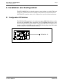
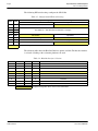
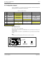
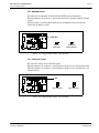
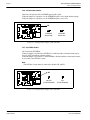
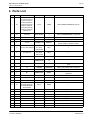
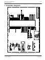
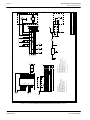
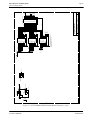
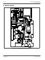
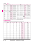
S1D13506 LCD/CRT/TV Controller
S5U13506P00C100 PCI Evaluation
Board User Manual
Document Number: X25B-G-014-02
Status: Revision 2.0
Issue Date: 2009/03/02
© SEIKO EPSON CORPORATION 2006 - 2009. All Rights Reserved.
Information in this document is subject to change without notice. You may download and use this document, but only for your own use in
evaluating Seiko Epson/EPSON products. You may not modify the document. Epson Research and Development, Inc. disclaims any
representation that the contents of this document are accurate or current. The Programs/Technologies described in this document may contain
material protected under U.S. and/or International Patent laws.
EPSON is a registered trademark of Seiko Epson Corporation. All other Trademarks are the property of their respective owners.
Page 2
Epson Research and Development
Vancouver Design Center
THIS PAGE LEFT BLANK
S1D13506
X25B-G-014-02
S5U13506P00C100 PCI Evaluation Board User Manual
Issue Date: 2009/03/02
Epson Research and Development
Vancouver Design Center
Page 3
Table of Contents
1
Introduction . . . . . . . . . . . . . . . . . . . . . . . . . . . . . . . . . . . . . . . . 5
2
Features . . . . . . . . . . . . . . . . . . . . . . . . . . . . . . . . . . . . . . . . . . 6
3
Installation and Configuration . . . . . . . . . . . . . . . . . . . . . . . . . . . . . . 7
3.1 Configuration DIP Switches . . . . . . . . . . . . . . . . . . . . . . . . . . 7
3.2 Configuration Jumpers . . . . . . . . . . . . . . . . . . . . . . . . . . . . 9
4
Technical Description . . . . . . . . . . . . . . .
4.1 PCI Bus Support . . . . . . . . . . . . . .
4.2 Non-PCI Host Interface Support . . . . . . . .
4.2.1 CPU Interface Pin Mapping . . . . . . . . . .
4.2.2 CPU Bus Connector Pin Mapping . . . . . .
4.3 LCD Support . . . . . . . . . . . . . . . .
4.3.1 LCD Interface Pin Mapping . . . . . . . . . .
4.3.2 Buffered LCD Connector . . . . . . . . . . .
4.4 CRT/TV Support . . . . . . . . . . . . . .
4.4.1 CRT/TV Interface Pin Mapping . . . . . . . .
4.4.2 CRT Support . . . . . . . . . . . . . . . . .
4.4.3 TV Support . . . . . . . . . . . . . . . . . .
4.5 Current consumption measurement . . . . . . .
5
References . . . . . . . . . . . . . . . . . . . . . . . . . . . . . . . . . . . . . . . 22
5.1 Documents . . . . . . . . . . . . . . . . . . . . . . . . . . . . . . . 22
5.2 Document Sources . . . . . . . . . . . . . . . . . . . . . . . . . . . . 22
6
Parts List . . . . . . . . . . . . . . . . . . . . . . . . . . . . . . . . . . . . . . . . 23
7
Schematic Diagrams . . . . . . . . . . . . . . . . . . . . . . . . . . . . . . . . . . 25
8
Board Layout . . . . . . . . . . . . . . . . . . . . . . . . . . . . . . . . . . . . . . 30
9
Technical Support . . . . . . . . . . . . . . . . . . . . . . . . . . . . . . . . . . . 31
9.1 EPSON LCD/CRT Controllers (S1D13506) . . . . . . . . . . . . . . . . . . 31
S5U13506P00C100 PCI Evaluation Board User Manual
Issue Date: 2009/03/02
. . .
. .
. .
. . .
. . .
. .
. . .
. . .
. .
. . .
. . .
. . .
. .
.
.
.
.
.
.
.
.
.
.
.
.
.
. . . . . .
. . . . .
. . . . .
. . . . . . .
. . . . . . .
. . . . .
. . . . . . .
. . . . . . .
. . . . .
. . . . . . .
. . . . . . .
. . . . . . .
. . . . .
.
.
.
.
.
.
.
.
.
.
.
.
.
. . . . . . .
. . . . . .
. . . . . .
. . . . . . . .
. . . . . . . .
. . . . . .
. . . . . . . .
. . . . . . . .
. . . . . .
. . . . . . . .
. . . . . . . .
. . . . . . . .
. . . . . .
14
14
14
15
16
18
19
20
21
21
21
21
21
S1D13506
X25B-G-014-02
Page 4
Epson Research and Development
Vancouver Design Center
THIS PAGE LEFT BLANK
S1D13506
X25B-G-014-02
S5U13506P00C100 PCI Evaluation Board User Manual
Issue Date: 2009/03/02
Epson Research and Development
Vancouver Design Center
Page 5
1 Introduction
This manual describes the setup and operation of the S5U13505P00C100 PCI Evaluation
Board. The S5U13506P00C100 is designed as an evaluation platform for the S1D13506
Color LCD/CRT/TV Controller chip.
This document is updated as appropriate. Please check the Epson Research and Development website at http://www.erd.epson.com for the latest revision of this document before
beginning any development.
We appreciate your comments on our documentation. Please contact us via email at
[email protected].
S5U13506P00C100 PCI Evaluation Board User Manual
Issue Date: 2009/03/02
S1D13506
X25B-G-014-02
Page 6
Epson Research and Development
Vancouver Design Center
2 Features
The S5U13506P00C100 features the following:
• S1D13506 Color LCD/CRT/TV controller chip
• PCI bus operation using on-board PCI bridge
• Headers for connecting to a 3.3V host bus interface (5V host bus interface also possible
with modifications to the board)
• 1Mx16 EDO DRAM
• Configuration options
• Headers for S1D13506 current consumption measurements
• 4/8-bit 3.3V or 5V monochrome passive LCD panel support
• 4/8/16-bit 3.3V or 5V color passive LCD panel support
• 9/12/18-bit 3.3V or 5V TFT/D-TFD LCD panel support
• Embedded RAMDAC for CRT and TV support
• Software initiated Power Save Mode
S1D13506
X25B-G-014-02
S5U13506P00C100 PCI Evaluation Board User Manual
Issue Date: 2009/03/02
Epson Research and Development
Vancouver Design Center
Page 7
3 Installation and Configuration
The S5U13506P00C100 is designed to support as many platforms as possible. The board
incorporates a DIP switch and several jumpers which allow both evaluation board and
S1D13506 LCD controller settings to be configured for a specified evaluation platform.
3.1 Configuration DIP Switches
The S1D13506 LCD controller has 16 configuration inputs (MD[15:0]) which are read on
the rising edge of RESET#. Where appropriate, the S5U13506P00C100 hard-wires some
of these configuration inputs, but in order to configure the S1D13505 for multiple host bus
interfaces an eight-position DIP switch is required. The following figure shows the location
of DIP switch S1 on the S5U13506P00C100 board.
DIP Switch - S1
Figure 3-1: Configuration DIP Switch (S1) Location
S5U13506P00C100 PCI Evaluation Board User Manual
Issue Date: 2009/03/02
S1D13506
X25B-G-014-02
Page 8
Epson Research and Development
Vancouver Design Center
The following DIP switch settings configure the S1D13506.
Table 3-1: Configuration DIP Switch Settings
Value of this pin at rising edge of RESET# is used to configure:
Switch Signal
Closed/On=1
Open/Off=0
WAIT# is always driven.
WAIT# is tristated when S1D13506 is not selected
S1-1
MD15
S1-2
MD1
S1-3
MD2
S1-4
MD3
S1-5
MD4
Little Endian
Big Endian
S1-6
MD5
WAIT# is active high
WAIT# is active low
S1-7
MD11
S1-8
MD12
See Table 3-2:, “Host Bus Interface Selection” on page 8
See Table 3-2:, “Host Bus Interface Selection” on page 8
BUSCLK input not divided
BUSCLK input divided by 2
= Required configuration when used in a PCI environment
The following table shows the Host Bus Interface options available. The host bus interface
is selected according to the evaluation platform to be used.
Table 3-2: Host Bus Interface Selection
MD11
MD3
MD2
MD1
Host Bus Interface
0
0
0
0
SH-4/SH-3
0
0
0
1
MC68K Bus 1
0
0
1
0
MC68K Bus 2
0
0
1
1
Generic
0
1
0
0
Reserved
0
1
0
1
MIPS/ISA
0
1
1
0
PowerPC
0
1
1
1
PC Card
1
1
1
1
Philips PR31500/PR31700 / Toshiba TX3912
= Required configuration when used in a PCI environment
S1D13506
X25B-G-014-02
S5U13506P00C100 PCI Evaluation Board User Manual
Issue Date: 2009/03/02
Epson Research and Development
Vancouver Design Center
Page 9
3.2 Configuration Jumpers
The S5U13505B00C has seven jumper blocks which configure various board settings. The
jumper positions for each function are shown below.
Table 3-3: Jumper Settings
Jumper
Function
Position 1-2
Position 2-3
Jumper Off
JP1
BUSCLK Selection
JP2
CLKI Selection
BUSCLK from U2 oscillator
BUSCLK from H2 header
n/a
CLKI from U3 oscillator
CLKI is the same as BUSCLK
n/a
JP3
VDD current
Normal operation
n/a
Current measurement for
VDD
JP4
DACVDD current
Normal operation
n/a
Current measurement for
DACVDD
JP5
LCD Panel Voltage
+5V LCDVCC
+3.3V LCDVCC
n/a
JP6
Panel Enable Polarity
LCDPWR active high
LCDPWR active low
n/a
JP7
PCI FPGA enable
Disable FPGA for non-PCI
host
n/a
Enable FPGA for PCI host
JP8
IREF for CRT/TV DAC
4.6mA for CRT
9.2mA for TV
n/a
= Default configuration
JP1 - BUSCLK Selection
JP1 selects the source for BUSCLK.
When the jumper is at position 1-2, the BUSCLK source is provided by the oscillator at U2
(default setting).
When the jumper is at position 2-3, the BUSCLK source is provided by the non-PCI host
system.
Note
When used in a PCI environment, JP1 must be set to the 1-2 position.
JP1
BUSCLK from
Oscillator (U2)
BUSCLK
from H2
Figure 3-2: Configuration Jumper (JP1) Location
S5U13506P00C100 PCI Evaluation Board User Manual
Issue Date: 2009/03/02
S1D13506
X25B-G-014-02
Page 10
Epson Research and Development
Vancouver Design Center
JP2 - CLKI Selection
JP2 selects the source for CLKI.
When the jumper is at position 1-2, the CLKI source is provided by the oscillator at U3
(default setting).
When the jumper is at position 2-3, the CLKI source is the same as BUSCLK (provided by
the non-PCI host system).
JP2
CLKI from
Oscillator (U3)
CLKI same
as BUSCLK
Figure 3-3: Configuration Jumper (JP2) Location
JP3 - VDD current
JP3 allows the measurement of S1D13505 VDD current consumption.
When the jumper is at position 1-2, the evaluation board is operating normally (default
setting).
When no jumper is installed, VDD current consumption can be measured by connecting an
ammeter to JP3.
JP3
Normal
Operation
CoreVDD
Measurement
Figure 3-4: Configuration Jumper (JP3) Location
S1D13506
X25B-G-014-02
S5U13506P00C100 PCI Evaluation Board User Manual
Issue Date: 2009/03/02
Epson Research and Development
Vancouver Design Center
Page 11
JP4 - DACVDD current
JP4 allows the measurement of S1D13505 DACVDD current consumption.
When the jumper is at position 1-2, the evaluation board is operating normally (default
setting).
When no jumper is installed, DACVDD current consumption can be measured by
connecting an ammeter to JP4.
JP4
Normal
Operation
CoreVDD
Measurement
Figure 3-5: Configuration Jumper (JP4) Location
JP5 - LCD panel voltage
JP5 selects the voltage level to the LCD panel.
When the jumper is at position 1-2, the LCD panel voltage level is configured for 5.0V.
When the jumper is at position 2-3, the LCD panel voltage level is configured for 3.3V
(default setting).
JP5
+5V LCDVCC
+3.3 LCDVCC
Figure 3-6: Configuration Jumper (JP5) Location
S5U13506P00C100 PCI Evaluation Board User Manual
Issue Date: 2009/03/02
S1D13506
X25B-G-014-02
Page 12
Epson Research and Development
Vancouver Design Center
JP6 - Panel Enable Polarity
JP6 selects the polarity of the LCDPWR panel enable signal.
When the jumper is at position 1-2, the LCDPWR signal is active high (default setting).
When the jumper is at position 2-3, the LCDPWR signal is active low.
JP6
LCDPWR
Active High
LCDPWR
Active Low
Figure 3-7: Configuration Jumper (JP6) Location
JP7 - PCI FPGA Enable
JP7 controls the PCI FPGA.
When no jumper is installed, the PCI FPGA is enabled and the evaluation board may be
used in a PCI environment (default setting).
When the jumper is in position 1-2, the PCI FPGA is disabled and the evaluation board may
be used with a non-PCI host system.
Note
Non-PCI host system must be connected to headers H1 and H2.
JP7
non-PCI
(FPGA Disabled)
PCI
(FPGA Enabled)
Figure 3-8: Configuration Jumper (JP7) Location
S1D13506
X25B-G-014-02
S5U13506P00C100 PCI Evaluation Board User Manual
Issue Date: 2009/03/02
Epson Research and Development
Vancouver Design Center
Page 13
JP8 - IREF for CRT/TV DAC
JP8 selects the magnitude of the IREF current used by the embedded RAMDAC.
When the jumper is at position 1-2, the IREF current is 4.6mA. This setting is used for CRT
display.
When the jumper is at position 2-3, the IREF current is 9.2mA. This setting is used for TV
display, but it may be used by CRT display as well.
JP8
IREF = 4.6mA
IREF = 9.2mA
Figure 3-9: Configuration Jumper (JP8) Location
S5U13506P00C100 PCI Evaluation Board User Manual
Issue Date: 2009/03/02
S1D13506
X25B-G-014-02
Page 14
Epson Research and Development
Vancouver Design Center
4 Technical Description
The S5U13506P00C100 operates with both PCI and non-PCI evaluation platforms. It
supports passive LCD panels (4/6/16-bit), TFT/D-TFD panels (9/12/18-bit), CRT displays
(analog RGB output) and TV (NTSC and PAL).
4.1 PCI Bus Support
The S5U13506P00C100 does not have on-chip PCI bus interface support. The
S5U13506P00C100 uses the PCI FPGA to support the PCI bus.
4.2 Non-PCI Host Interface Support
The S5U13506P00C100 is specifically designed to support a standard PCI bus
environment (using the PCI Bridge Adapter FPGA). However, the S5U13506P00C100 can
directly support many other Host Bus Interfaces. When the FPGA is disabled (using jumper
JP7), headers H1 and H2 provide the necessary IO pins to interface to the Host Bus Interfaces listed in Table 4-4:, “CPU Interface Pin Mapping”.
Note
The S5U13506P00C100 is designed to work only with 3.3V systems. To use it with a
5V system, some modifications must be done to the board as follows:
1. Replace the 3.3V DRAM (U6) on the board with a 5V DRAM.
2. Cut the trace between JP9-2 and JP9-3 on the solder side of the board.
3. Connect JP9-1 and JP9-2. This will set IOVDD to 5V.
S1D13506
X25B-G-014-02
S5U13506P00C100 PCI Evaluation Board User Manual
Issue Date: 2009/03/02
Epson Research and Development
Vancouver Design Center
Page 15
4.2.1 CPU Interface Pin Mapping
The functions of the S1D13506 host interface pins are mapped to each host bus interface
according to the following table.
Table 4-4: CPU Interface Pin Mapping
Philips
PR31500
/PR31700
Toshiba
TX3912
A20
ALE
ALE
A12
A19
/CARDREG
CARDREG*
A18
A13
A18
/CARDIORD
CARDIORD*
A17
A17
A14
A17
/CARDIOWR
CARDIOWR*
SA[16:13]
A[16:13]
A[16:13]
A[15:18]
A[16:13]
SA[12:1]
A[12:1]
A[12:1]
A[19:30]
A[12:1]
A[12:1]
A[12:1]
A0
A0
Pin
Names
Generic
Hitachi
SH-4/SH-3
MIPS/ISA
Motorola
MC68K
Bus 1
Motorola
MC68K
Bus 2
AB20
A20
A20
LatchA20
A20
A20
A11
AB19
A19
A19
SA19
A19
A19
AB18
A18
A18
SA18
A18
AB17
A17
A17
SA17
AB[16:13] A[16:13]
A[16:13]
AB[12:1]
A[12:1]
S1D13505
A[12:1]
1
Motorola
PC Card
PowerPC
A01
SA0
LDS#
A0
A31
A01
Connected to VDD
AB0
A0
DB[15:8]
D[15:0]
D[15:8]
SD[15:0]
D[15:8]
D[31:24]
D[0:7]
D[15:0]
D[23:16]
D[23:16]
DB[7:0]
D[7:0]
D[7:0]
SD[7:0]
D[7:0]
D[23:16]
D[8:15]
D[7:0]
D[31:24]
D[31:24]
WE1#
WE1#
WE1#
SBHE#
UDS#
DS#
BI
-CE2
/CARDxCSH
CARDxCSH*
M/R#
External Decode
Connected to VDD
CS#
External Decode
Connected to VDD
BUSCLK
BCLK
CKIO
CLK
BS#
Connected
to VDD
BS#
Connected to
VDD
CLK
AS#
RD/WR#
RD1#
RD/WR#
Connected to
VDD
RD#
RD0#
RD#
WE0#
WE0#
WAIT#
RESET#
CLK
CLKOUT
CLK
AS#
TS
Connected
to VDD
R/W#
R/W#
RD/WR
-CE1
/CARDxCSL
CARDxCSL*
MEMR#
Connected
to VDD
SIZ1
TSIZ0
-OE
/RD
RD*
WE0#
MEMW#
Connected
to VDD
SIZ0
TSIZ1
-WE
/WE
WE*
WAIT#
RDY#
/WAIT#
IOCHRDY
TA
-WAIT
RESET#
RESET#
inverted
RESET
RESET#
inverted
RESET
DTACK# DSACK1#
RESET#
RESET#
DCLKOUT
DCLKOUT
Connected to VDD
/CARDxWAIT CARDxWAIT*
RESET#
PON*
Note
1
A0 for these busses is not used internally by the S1D13506.
S5U13506P00C100 PCI Evaluation Board User Manual
Issue Date: 2009/03/02
S1D13506
X25B-G-014-02
Page 16
Epson Research and Development
Vancouver Design Center
4.2.2 CPU Bus Connector Pin Mapping
The pinouts for Connector H1 are listed in the following table.
Table 4-5: CPU/BUS Connector (H1) Pinout
Pin No.
1
2
3
4
5
6
7
8
9
10
11
12
13
14
15
16
17
18
19
20
21
22
23
24
25
26
27
28
29
30
31
32
33
34
S1D13506
X25B-G-014-02
Function
Connected to DB0 of the S1D13506
Connected to DB1 of the S1D13506
Connected to DB2 of the S1D13506
Connected to DB3 of the S1D13506
Ground
Ground
Connected to DB4 of the S1D13506
Connected to DB5 of the S1D13506
Connected to DB6 of the S1D13506
Connected to DB7 of the S1D13506
Ground
Ground
Connected to DB8 of the S1D13506
Connected to DB9 of the S1D13506
Connected to DB10 of the S1D13506
Connected to DB11 of the S1D13506
Ground
Ground
Connected to DB12 of the S1D13506
Connected to DB13 of the S1D13506
Connected to DB14 of the S1D13506
Connected to DB15 of the S1D13506
Connected to RESET# of the S1D13506
Ground
Ground
Ground
+12 volt supply, required in non-PCI applications
+12 volt supply, required in non-PCI applications
Connected to WE0# of the S1D13506
Connected to WAIT# of the S1D13506
Connected to CS# of the S1D13506
Connected to MR# of the S1D13506
Connected to WE1# of the S1D135065
S1D13506 supply, provided by the S5U13506P00C100
S5U13506P00C100 PCI Evaluation Board User Manual
Issue Date: 2009/03/02
Epson Research and Development
Vancouver Design Center
Page 17
The pinouts for Connector H2 are listed in the following table.
Table 4-6: CPU/BUS Connector (H2) Pinout
Pin No.
Function
1
Connected to AB0 of the S1D13506
2
Connected to AB1 of the S1D13506
3
Connected to AB2 of the S1D13506
4
Connected to AB3 of the S1D13506
5
Connected to AB4 of the S1D13506
6
Connected to AB5 of the S1D13506
7
Connected to AB6 of the S1D13506
8
Connected to AB7 of the S1D13506
9
Ground
10
Ground
11
Connected to AB8 of the S1D13506
12
Connected to AB9 of the S1D13506
13
Connected to AB10 of the S1D13506
14
Connected to AB11 of the S1D13506
15
Connected to AB12 of the S1D13506
16
Connected to AB13 of the S1D13506
17
Ground
18
Ground
19
Connected to AB14 of the S1D13506
20
Connected to AB15 of the S1D13506
21
Connected to AB16 of the S1D13506
22
Connected to AB17 of the S1D13506
23
Connected to AB18 of the S1D13506
24
Connected to AB19 of the S1D13506
25
Ground
26
Ground
27
+5 volt supply, required in non-PCI applications
28
+5 volt supply, required in non-PCI applications
29
Connected to RD/WR# of the S1D13506
30
Connected to BS# of the S1D13506
31
Connected to S1D13506 BUSCLK if JP1 is in position 2-3
32
Connected to RD# of the S1D13506
33
Connected to AB20 of the S1D13506
34
Not connected
S5U13506P00C100 PCI Evaluation Board User Manual
Issue Date: 2009/03/02
S1D13506
X25B-G-014-02
Page 18
Epson Research and Development
Vancouver Design Center
4.3 LCD Support
The S1D13506 supports 4/8-bit dual and single passive monochrome panels, 4/8/16-bit
dual and single passive color panels, and 9/12/18-bit active matrix color TFT/D-TFD
panels. All necessary signals are provided on the 40-pin LCD connector (J1). The interface
signals are alternated with grounds on the cable to reduce cross-talk and noise. When
supporting an 18-bit TFT/D-TFD panel, the S1D13505 can display 64K of a possible 256K
colors because only 16 of the18 bits of LCD data are available from the S1D13505. For
details, refer to the S1D13506 Hardware Functional Specification, document number
X25B-A-001-xx.
For S1D13506 FPDAT[15:0] pin mapping for various types of panel see Table 4-7:, “LCD
Signal Connector (J4)” on page 19.
S1D13506
X25B-G-014-02
S5U13506P00C100 PCI Evaluation Board User Manual
Issue Date: 2009/03/02
Epson Research and Development
Vancouver Design Center
Page 19
4.3.1 LCD Interface Pin Mapping
Table 4-7: LCD Signal Connector (J4)
S1D13505
Pin Names
Connector
Pin No.
Monochrome Passive
Panels
Single
4-bit
FPDAT0
FPDAT1
FPDAT2
FPDAT3
FPDAT4
FPDAT5
FPDAT6
FPDAT7
FPDAT8
FPDAT9
FPDAT10
FPDAT11
FPDAT12
FPDAT13
FPDAT14
FPDAT15
FPSHIFT
DRDY
FPLINE
FPFRAME
1 and 6
3
5
7
9
11
13 and 4
15
17
19
21
23
25
27
29
31
33
35 and 38
37
39
2 and 8-26
GND
(Even Pins)
N/C
28
N/C
30
LCDVCC
32
+12V
34
N/C
36
NC (pin 75)2
40
D0
D1
D2
D3
8-bit
D0
D1
D2
D3
D4
D5
D6
D7
Color Passive Panels
Dual
Single
8-bit
LD0
LD1
LD2
LD3
UD0
UD1
UD2
UD3
4-bit
MOD
D0
D1
D2
D3
Single
Single
Format 1
Format 2
8-bit
D0
D1
D2
D3
D4
D5
D6
D7
8-bit
D0
D1
D2
D3
D4
D5
D6
D7
FPSHIFT2
Single
Dual
16-Bit 8-bit
D0
LD0
D1
LD1
D2
LD2
D3
LD3
D8
UD0
D9
UD1
D10
UD2
D11
UD3
D4
D5
D6
D7
D12
D13
D14
D15
FPSHIFT
MOD
FPLINE
FPFRAME
16-bit
LD0
LD1
LD2
LD3
UD0
UD1
UD2
UD3
LD4
LD5
LD6
LD7
UD4
UD5
UD6
UD7
Color TFT/D-TFD
Panels
9-bit
R2
R1
R0
G2
G1
G0
B2
B1
B0
12-bit
R3
R2
R1
G3
G2
G1
B3
B2
B1
R0
G0
B0
18-bit
R5
R4
R3
G5
G4
G3
B5
B4
B3
R2
R1
G2
G1
G0
B2
B1
DRDY
GND
N/C
N/C
+5V or +3.3V according to JP5
+12V
N/C
Panel Enable, active low (LCDPWR)2
= Driven low
Note
1
For FPDATxx to LCD interface hardware connections refer to the Display Interface
AC Timing section of the S1D13506 Hardware Functional Specification, document
number X25B-A-001-xx.
2 The S5U13506B00C was designed using S1D13506 pin 75 (LCDPWR) to control the
LCD bias power. This design is no longer supported. Applications should use one of
the available GPIO pins to control the LCD bias power allowing for software control
of power sequencing delays. For further information on LCD power sequencing, see
the S1D13506 Programming Notes and Examples, document number X25B-G-003xx.
S5U13506P00C100 PCI Evaluation Board User Manual
Issue Date: 2009/03/02
S1D13506
X25B-G-014-02
Page 20
Epson Research and Development
Vancouver Design Center
4.3.2 Buffered LCD Connector
J4 provides the same LCD panel signals as those directly from S1D13505, but with voltageadapting buffers which can be set to 3.3V or 5V. Pin 32 on this connector provides power
for the LCD panel logic at the same voltage as the buffer power supply.
S1D13506
X25B-G-014-02
S5U13506P00C100 PCI Evaluation Board User Manual
Issue Date: 2009/03/02
Epson Research and Development
Vancouver Design Center
Page 21
4.4 CRT/TV Support
4.4.1 CRT/TV Interface Pin Mapping
CRT/TV signals are supplied on a standard CRT connector (J2), Composite Video
connector (J1), and S-Video connector (J3):
Table 4-8: CRT/TV Interface Pin Mapping
S1D13506
Pin Name
CRT
Composite Video
S-Video
HRTC
Horizontal retrace
N/A
N/A
VRTC
Vertical retrace
N/A
N/A
RED
Red
N/A
Luminance
GREEN
Green
Composite
N/A
BLUE
Blue
N/A
Chrominance
4.4.2 CRT Support
CRT support is provided on connector J2 via the S1D13506 embedded RAMDAC. An
external current reference is implemented to provide the necessary RAMDAC output gain.
The reference current (IREF) should be set to 4.6mA using jumper JP8.
Note
When IREF is set to 4.6mA, the DAC Output Select bit (REG[05Bh] bit 3) must be set
to 1.
CRT output is not available when TV output is enabled.
4.4.3 TV Support
The S1D13506 supports PAL or NTSC TV output. Composite Video is available on
connector J1 and S-Video is available on connector J3. An external current reference is
implemented to provide the necessary RAMDAC output gain. The reference current should
be set to 9.2mA using jumper JP8.
TV output is not available when CRT output is enabled. PAL and NTSC modes cannot be
enabled at the same time.
4.5 Current consumption measurement
The evaluation board has 2 headers, JP3 and JP4, which allow the independent
measurement of S1D13506 VDD and DACVDD current consumption. To measure the
current, remove the appropriate jumper and connect an ammeter to the corresponding
header pins.
S5U13506P00C100 PCI Evaluation Board User Manual
Issue Date: 2009/03/02
S1D13506
X25B-G-014-02
Page 22
Epson Research and Development
Vancouver Design Center
5 References
5.1 Documents
• Epson Research and Development, Inc., S1D13506 Hardware Functional Specification,
Document Number X25B-A-001-xx.
• Epson Research and Development, Inc., S1D13506 Programming Notes and Examples,
Document Number X25B-G-003-xx.
5.2 Document Sources
• Epson Research and Development Website: http://www.erd.epson.com.
S1D13506
X25B-G-014-02
S5U13506P00C100 PCI Evaluation Board User Manual
Issue Date: 2009/03/02
Epson Research and Development
Vancouver Design Center
Page 23
6 Parts List
Item Quantity
Reference
Part
Footprint
Comments
0.1uF
C0805
Kemet C0805C104K4RACTU generic
—
Kemet T491D686K010AS or equivalent
1
38
C1,C2,C3,C4,C5,C6,
C7,C8,C9,C10,C11,
C12,C13,C16,C17,
C18,C19,C20,C22,
C23,C24,C27,C29,
C30,C31,C40,C41,
C42,C43,C44,C45,
C46,C47,C48,C49,
C50,C51,C52
2
6
C14,C15,C21,C36,
C37,C38
68uF/10V/10%
3
2
C35,C39
33uF/20V/10%
—
Kemet T491D336K020AS or equivalent
4
3
D1,D2,D3
BAV99
SOT23
Fairchild Semiconductor BAV99
5
2
H1,H2
HEADER 17X2
HDR2X17
Thomas&Betts 609-3407 altern.
Samtec TSW-117-05-G-D or equiv.
6
5
JP1,JP2,JP5,JP6,JP8
Header 3x1,
0.1" pitch,
unshrouded
SIP3
—
7
3
JP3,JP4,JP7
Header 2x1,
0.1" pitch,
unshrouded
SIP2
—
8
1
J1
C-VIDEO
—
CUI RCJ-014
9
1
J2
VGA
CONNECTOR
DB15/PS2CO
N
NorComp 181-015-213R561 or equivalent
105
1
J3
S-VIDEO
—
Kycon KMDGX-4S-BS-99 or equivalent Mini DIN
4 pin
11
1
J4
CON40A
HDR2X20A
Samtec TST-120-01-G-D or equivalent
12
5
L1,L2,L3,L4,L5
Ferrite Bead
INDUCTOR1
Steward 28F0181-ISR-10
SOT23
Fairchild Semiconductor MMBT2222A or
equivalent
13
1
Q1
MMBT2222A
14
3
R1,R2,R36
100K,5%
R0805
—
15
3
R4,R5,R6
150R,1%
R0805
generic
16
1
R7
0R
R0805
—
17
16
R9,R10,R11,R12,R13,
R14,R15,R16,R17,
R18,R20,R39,R40,
R41,R42,R44
15K,5%
R0805
—
18
1
R19
1.5K,1%
R0805
generic
19
4
R21,R37,R38,R43
1K,1%
R0805
—
20
1
R23
69.8R,1%
R0805
—
21
1
R24
140R,1%
R0805
generic
22
1
S1
SW DIP-8
DIPSW8
Grayhill 76SB08S
23
1
U1
S1D13506F00A
TQFP128
Epson S1D13506F00A
24
1
U2
40MHz
DIP14
Epson SG8002DB, 40MHz socketed
25
1
U3
25.175MHz
DIP14
Epson SG8002DB, 25MHz socketed
S5U13506P00C100 PCI Evaluation Board User Manual
Issue Date: 2009/03/02
S1D13506
X25B-G-014-02
Page 24
Epson Research and Development
Vancouver Design Center
Item Quantity
Reference
Part
Footprint
Comments
26
1
U4
14.31818MHz
DIP14
Epson SG8002DB, 14.31818MHz socketed
27
1
U5
LT1117CM-3.3
DDPAK-2
Linear Technologies LT1117CM-3.3
28
1
U6
DRAM 1Mx16SOJ, Lead free
SOJ42
ISSI IS41LV16100B-50KL
29
1
U7
LT1117CST-3.3
—
Linear Technologies LT1117CST-3.3
INVERTER
SINGLE
NC7S04
SC70-5
Fairchild Semiconductor NC7S04P5
30
1
U8
31
3
U9,U10,U11
74AHC244
SO20W
TI 74AHC244
TQFP144
Altera EPF6016TC144-2
DIP8
Altera EPC1PI8N programmed, socketed
32
1
U14
EPF6016TC14
4-2
33
1
U15
EPC1PI8N
S1D13506
X25B-G-014-02
S5U13506P00C100 PCI Evaluation Board User Manual
Issue Date: 2009/03/02
D
C
B
A
4
+5V
IOVDD
1
0.1uF
C13
C16
0.1uF
0.1uF
C3
IOVDD
0.1uF
C2
IOVDD
BCLK
0.1uF
C1
IOVDD
7
14
7
14
7
14
VCC
GND
NC
OUT
NC
3
U5
LT1117CM-3.3
VIN
8
1
3
2
1
CLKI
2
2
C15
68uF/10V/10%
VOUT
+
DACVDD
+
5
+3.3V
C14
68uF/10V/10%
3.3V
BUSCLK
FPGA_CLK
CLKI2
2
Not populated for S5U13505B00C
FERRITE BEAD
L2
8
1
CLKI
JP2
14.31818MHz
OUT
1
2
3
BUSCLK
JP1
8
1
25.175MHz
FERRITE BEAD
L1
U4
GND
VCC
U3
OUT
NC
40MHz
BUSCLK
U2
GND
VCC
ADJ
1
WAIT#
0.1uF
3
Not populated
+5V
0.1uF
0.1uF
0.1uF
0.1uF
JP9
IOVDD SELECT +3.3V
IOVDD
0.1uF
4
DACVDD By-pass Capacitors (1/power pin)
C11
C12
C10
0.1uF
0.1uF
C8
DB[15:0]
AB[20:0]
COREVDD By-pass Capacitors (1/power pin)
C4
C5
C6
C7
CLKI
BUSCLK
4,5
M/R#
4,5
CS#
RESET#
4,5
4,5
RD/WR#
WE1#
WE0#
RD#
BS#
DB[15:0]
AB[20:0]
4
4,5
4,5
4,5
4,5
4,5
4,5
4,5
Short pin 2 and 3 of JP8 on PCB, solder side.
JP4
DAC CURRENT
DACVDD
JP3
CORE/IO CURRENT
IOVDD
3
2
1
2
1
2
1
2
1
S5U13506P00C100 PCI Evaluation Board User Manual
Issue Date: 2009/03/02
1
2
3
1
0.1uF
C9
31
30
29
28
27
26
25
24
23
22
21
20
19
18
17
16
DB0
DB1
DB2
DB3
DB4
DB5
DB6
DB7
DB8
DB9
DB10
DB11
DB12
DB13
DB14
DB15
5
70
98
106
14
32
50
68
78
87
96
110
99
102
104
12
33
55
72
97
109
69
13
15
4
5
11
10
9
8
7
6
3
2
1
128
127
126
125
124
123
122
121
120
119
118
117
116
115
114
113
112
111
AB0
AB1
AB2
AB3
AB4
AB5
AB6
AB7
AB8
AB9
AB10
AB11
AB12
AB13
AB14
AB15
AB16
AB17
AB18
AB19
AB20
5
S1D13506F00A
TESTEN
DAC_VSS1
DAC_VSS2
VSS1
VSS2
VSS3
VSS4
VSS5
VSS6
VSS7
VSS8
DAC_VDD1
DAC_VDD2
DAC_VDD3
VDD1
VDD2
VDD3
VDD4
VDD5
VDD6
CLKI
BUSCLK
WAIT#
CS#
M/R#
RESET#
RD/WR#
WE1#
WE0#
RD#
BS#
DB0
DB1
DB2
DB3
DB4
DB5
DB6
DB7
DB8
DB9
DB10
DB11
DB12
DB13
DB14
DB15
AB0
AB1
AB2
AB3
AB4
AB5
AB6
AB7
AB8
AB9
AB10
AB11
AB12
AB13
AB14
AB15
AB16
AB17
AB18
AB19
AB20
U1
6
IREF
VRTC
HRTC
BLUE
GREEN
RED
FPDAT0
FPDAT1
FPDAT2
FPDAT3
FPDAT4
FPDAT5
FPDAT6
FPDAT7
FPDAT8
FPDAT9
FPDAT10
FPDAT11
FPDAT12
FPDAT13
FPDAT14
FPDAT15
FPFRAME
FPLINE
FPSHIFT
DRDY
CLKI2
LCDPWR
RAS#
LCAS#
UCAS#
WE#
MD0
MD1
MD2
MD3
MD4
MD5
MD6
MD7
MD8
MD9
MD10
MD11
MD12
MD13
MD14
MD15
MA0
MA1
MA2
MA3
MA4
MA5
MA6
MA7
MA8
MA9/GPIO3
MA10/GPIO1
MA11/GPIO2
6
101
108
107
105
103
100
79
80
81
82
83
84
85
86
88
89
90
91
92
93
94
95
73
74
77
76
71
75
R3
IOVDD
LCDPWR#
RAS#
LCAS#
UCAS#
WE#
MD[15..0]
R2
100K,5%
MA[9..0]
IREF
VRTC
HRTC
BLUE
GREEN
RED
CLKI2
FPFRAME
FPLINE
FPSHIFT
FPDAT[15..0] DRDY
FPDAT[15..0]
100K,5%
MD[15..0]
R1
100K,5%
IOVDD
MA[9..0]
Date:
7
Monday, December 11, 2006
Size
Document Number
Custom
S5U13505/6B00C PCI Bus: 13506F00A Chip
Epson Research & Development, Inc.
FPDAT0
FPDAT1
FPDAT2
FPDAT3
FPDAT4
FPDAT5
FPDAT6
FPDAT7
FPDAT8
FPDAT9
FPDAT10
FPDAT11
FPDAT12
FPDAT13
FPDAT14
FPDAT15
MD0
MD1
MD2
MD3
MD4
MD5
MD6
MD7
MD8
MD9
MD10
MD11
MD12
MD13
MD14
MD15
35
37
39
41
43
45
47
49
48
46
44
42
40
38
36
34
54
51
52
53
MA0
MA1
MA2
MA3
MA4
MA5
MA6
MA7
MA8
MA9
MA10
MA11
61
63
65
67
66
64
62
60
58
56
59
57
7
2
2
2
2
2
2
3
3
3
3
3
Sheet
Not populated
3
2
2
2
2
2
2
1
8
8
of
5
Rev
2.0
D
C
B
A
Epson Research and Development
Vancouver Design Center
Page 25
7 Schematic Diagrams
Figure 7-1: S5U13506P00C100 Evaluation Board Schematics (1 of 5)
S1D13506
X25B-G-014-02
D
C
B
A
1
1
MA[9..0]
MD[15..0]
DRAM 1Mx16-SOJ
/OE
NC
NC
NC
/W
/RAS
/UCAS
/LCAS
A0
A1
A2
A3
A4
A5
A6
A7
A8R/A8
A9R/A9
NC
NC
U6
VSS
VSS
VSS
VCC
VCC
VCC
DQ0
DQ1
DQ2
DQ3
DQ4
DQ5
DQ6
DQ7
DQ8
DQ9
DQ10
DQ11
DQ12
DQ13
DQ14
DQ15
0R
1
2
3
4
5
6
7
8
MD0
MD1
MD2
MD3
MD4
MD5
MD6
MD7
MD8
MD9
MD10
MD11
MD12
MD13
MD14
MD15
16
15
14
13
12
11
10
9
R9
R10
R11
R12
R13
R14
R15
R16
R20 15K,5%
R17 15K,5%
R18 15K,5%
15K,5%
15K,5%
15K,5%
15K,5%
15K,5%
15K,5%
15K,5%
15K,5%
0.1uF
0.1uF
SW DIP-8
S1
C18
C17
IOVDD
0.1uF
C19
IOVDD
+5V
1
1
1
1
1
2
Note: Chip has internal tie low resistors
3
Note: Chip has internal tie low resistors
4
VRTC
HRTC
BLUE
GREEN
RED
0.1uF
C20
MD0 - not used
MD[3:1]= selects CPU bus interface
MD4 - 1=Little Endian, 0=Big Endian
MD5 - 1=WAIT# ACTIVE HIGH, 0=WAIT#ACTIVE LOW
MD[7:6] - Memory type set for Symetrical 1Mx16DRAM
MD8 - not used
MD9 - 1=SUSPEND PIN as GPO
MD10 - not used, but set to be active LOW LCDPWR (pin 75 NC)
MD11 - 1=Alternate,0=Primary Host Selection
MD12 - 1=BUSCLK input divide, 0=no divide
MD[14:13] - not used
MD15 - 1=WAIT# always driven, 0=WAIT# is tristated
0R
22
37
42
1
6
21
2
3
4
5
7
8
9
10
33
34
35
36
38
39
40
41
MD0 - 1=8bit, 0=16bit
MD[3:1]= selects CPU bus interface
MD4 - 1=Little Endian, 0=Big Endian
MD5 - 1=WAIT# ACTIVE HIGH, 0=WAIT#ACTIVE LOW
MD[7:6] - Memory type set for Symetrical 1Mx16DRAM
MD8 - not used
MD9 - 1=SUSPEND PIN as GPO
MD10 - active LOW LCDPWR/active HIGH GPO
MD11 - 1=Alternate,0=Primary Host Selection
MD12 - 1=BUSCLK input divide, 0=no divide
MD[15:13] - not used
R8
Not populated for S5U13506B00C
R7
Not populated for S5U13505B00C
29
11
12
32
13
14
30
31
17
18
19
20
23
24
25
26
27
28
16
15
Config setup for S1D13506:
MD10
MD6
MD9
MD1
MD2
MD3
MD4
MD5
MD11
MD12
MD0
MD15
MA0
MA1
MA2
MA3
MA4
MA5
MA6
MA7
MA8
MA9
Config setup for S1D13505:
MD[15..0]
WE#
1
MD[15..0]
RAS#
UCAS#
LCAS#
MA[9..0]
1
1
1
1
MD[15..0]
4
3
VIN
5
VOUT
2
150R,1%
R5
FERRITE BEAD
U7
LT1117CST-3.3
150R,1%
R4
L3
5
L4
+
6
R19 1.5K,1%
3
D3
BAV99
DACVDD
FERRITE BEAD
3
C21
68uF/10V/10%
150R,1%
R6
L5
6
D2
BAV99
DACVDD
FERRITE BEAD
3
D1
BAV99
DACVDD
2
1
1
3
2
1
2
1
2
ADJ
1
1K,1%
R21
IREF
B
Date:
Size
7
Thursday, October 03, 2002
Document Number
8
JP8
J1
J3
G
IREF
1
3
69.8R,1%
R23
S-VIDEO
G
C Y
C-VIDEO
Sheet
2
8
of
5
Not populated for S5U13505B00C
1
2
4
1
Not populated for S5U13505B00C
VGA CONNECTOR
J2
Not populated for
S5U13506B00C
140R,1%
R24
0R
R22
Q1
MMBT2222A
6
1
11
7
2
12
8
3
13
9
4
14
10
5
15
7
Epson Research & Development, Inc.
Title
S5U13505/6B00C PCI Bus: DRAM/Configuration/CRT Output
1
3
2
2
S1D13506
X25B-G-014-02
1
2
3
1
Rev
2.0
D
C
B
A
Page 26
Epson Research and Development
Vancouver Design Center
Figure 7-2: S5U13506P00C100 Evaluation Board Schematics (2 of 5)
S5U13506P00C100 PCI Evaluation Board User Manual
Issue Date: 2009/03/02
S5U13506P00C100 PCI Evaluation Board User Manual
Issue Date: 2009/03/02
NC
GND
1
4
1
2
3
JP6
LCD PW R SELECT
2
3
LCDVCC
4
1
FPDAT[15..0]
1
1
1
1
5
1
19
2
4
6
8
11
13
15
17
1
19
2
4
6
8
11
13
15
17
1
19
2
4
6
8
11
13
15
17
U9
74AHC244
1G
2G
1A1
1A2
1A3
1A4
2A1
2A2
2A3
2A4
U11
74AHC244
1G
2G
1A1
1A2
1A3
1A4
2A1
2A2
2A3
2A4
U10
74AHC244
1G
2G
1A1
1A2
1A3
1A4
2A1
2A2
2A3
2A4
6
VCC
GND
1Y1
1Y2
1Y3
1Y4
2Y1
2Y2
2Y3
2Y4
VCC
GND
1Y1
1Y2
1Y3
1Y4
2Y1
2Y2
2Y3
2Y4
VCC
GND
1Y1
1Y2
1Y3
1Y4
2Y1
2Y2
2Y3
2Y4
20
10
18
16
14
12
9
7
5
3
20
10
18
16
14
12
9
7
5
3
20
10
18
16
14
12
9
7
5
3
6
Note: 244 input side violates the spec of chip. At
5V, 244 logic high needs to be greater than 3.7V. Our
chip if set for 3.3V will not meet this input
requirement of the 244.
FPDAT8
FPDAT9
FPDAT10
FPDAT11
FPDAT12
FPDAT13
FPDAT14
FPDAT15
FPDAT0
FPDAT1
FPDAT2
FPDAT3
FPDAT4
FPDAT5
FPDAT6
FPDAT7
FPSHIFT
DRDY
FPLINE
FPFRAME
LCDPOW ER
FPDAT[15..0]
5
8
LCDP#
Sheet
CON40A
1
3
5
7
9
11
13
15
17
19
21
23
25
27
29
31
33
35
37
39
2
4
6
8
10
12
14
16
18
20
22
24
26
28
30
32
34
36
38
40
3
8
of
COLOR/MONO LCD CONNECTOR
J4
FPD0
FPD1
FPD2
FPD3
FPD4
FPD5
FPD6
FPD7
FPD8
FPD9
FPD10
FPD11
FPD12
FPD13
FPD14
FPD15
FPS
FPS2
FPL
FPF
Epson Research & Development, Inc.
0.1uF
C29
LCDVCC
0.1uF
C24
LCDVCC
0.1uF
LCDVCC
C23
7
5
Rev
2.0
VLCD
LCDVCC
+12V
VDDH
FPD6
FPD0
B
A
Date:
7
Document Number
Monday, December 11, 2006
Size
B
S5U13505/6B00C PCI Bus: LCD Headers
D
3
2
1
4
D
+5V
JP5
LCD VCC SELECT
+3.3V
3
C
1
LCDPW R
LCDPOWER
INVERTER SINGLE NC7S04
3
A Y
Vcc
U8
Input on 244 can take upto 5.5V as input high.
0.1uF
C22
IOVDD
LCDPW R#
2
5
IOVDD
2
C
B
A
1
1
Epson Research and Development
Vancouver Design Center
Page 27
Figure 7-3: S5U13506P00C100 Evaluation Board Schematics (3 of 5)
S1D13506
X25B-G-014-02
S1D13506
X25B-G-014-02
D
C
B
A
5
1
AD[31:0]
1
AD2
AD0
AD6
AD4
AD9
AD13
AD11
+5V
C/BE0#
PAR
5
5
STOP#
5
AD15
TRDY#
5
IDSEL
FRAME#
AD18
AD16
AD22
AD20
AD24
AD28
AD26
AD30
RST#
5
5
5
+5V
+12V
3
52
53
54
55
56
57
58
59
60
61
62
14
15
16
17
18
19
20
21
22
23
24
25
26
27
28
29
30
31
32
33
34
35
36
37
38
39
40
41
42
43
44
45
46
47
48
49
1
2
3
4
5
6
7
8
9
10
11
2
+
PCI-B
AD8
AD7
+3.3V
AD5
AD3
GND
AD1
+VI/O
ACK64#
+5V
+5V
RESERVED
GND
CLK
GND
REQ#
+VI/O
AD31
AD29
GND
AD27
AD25
+3.3V
C/BE3#
AD23
GND
AD21
AD19
+3.3V
AD17
C/BE2#
GND
IRDY#
+3.3V
DEVSEL#
GND
LOCK#
PERR#
+3.3V
SERR#
3.3V
C/BE1#
AD14
GND
AD12
AD10
GND
-12V
TCK
GND
TDO
+5V
+5V
INTB#
INTD#
PRSNT#1
RESERVED
PRSNT#2
PCIB1
+5V
C37
68uF/10V/10%
PCI-A
C/BE0#
+3.3V
AD6
AD4
GND
AD2
AD0
+VI/O
REQ64#
+5V
+5V
RESERVED
RST#
+VI/O
GNT#
GND
RESERVED
AD30
+3.3V
AD28
AD26
GND
AD24
IDSEL
+3.3V
AD22
AD20
GND
AD18
AD16
+3.3V
FRAME#
GND
TRDY#
GND
STOP#
+3.3V
SDONE
SBO#
GND
PAR
AD15
+3.3V
AD13
AD11
GND
AD9
TRST#
+12V
TMS
TDI
+5V
INTA#
INTC#
+5V
RESERVED
+VI/O
RESERVED
PCIA1
+
52
53
54
55
56
57
58
59
60
61
62
14
15
16
17
18
19
20
21
22
23
24
25
26
27
28
29
30
31
32
33
34
35
36
37
38
39
40
41
42
43
44
45
46
47
48
49
1
2
3
4
5
6
7
8
9
10
11
AD[31:0]
3
+5V
2
AD17
AD21
AD19
AD23
AD27
AD25
AD31
AD29
C38
68uF/10V/10%
+5V
AD1
AD5
AD3
AD8
AD7
AD12
AD10
4
+
+12V
5
5
SERR#
C/BE1#
5
5
5
5
5
5
PERR#
AD14
DEVSEL#
IRDY#
C/BE2#
C/BE3#
CLK
+5V
4
C39
33uF/20V/10%
1,5
1,5
AB[20:0]
DB[15:0]
5
5
1,5
1
1,5
1,5
1,5
1,5
RD/WR#
BCLK
WE0#
CS#
WE1#
RESET#
AB[20:0]
AB20
+5V
AB14
AB16
AB18
AB8
AB10
AB12
AB0
AB2
AB4
AB6
+12V
DB12
DB14
DB8
DB10
DB4
DB6
DB0
DB2
DB[15:0]
6
6
2
4
6
8
10
12
14
16
18
20
22
24
26
28
30
32
34
2
4
6
8
10
12
14
16
18
20
22
24
26
28
30
32
34
HEADER 17X2
1
3
5
7
9
11
13
15
17
19
21
23
25
27
29
31
33
H2
HEADER 17X2
1
3
5
7
9
11
13
15
17
19
21
23
25
27
29
31
33
H1
BS#
RD#
AB15
AB17
AB19
AB9
AB11
AB13
AB1
AB3
AB5
AB7
1,5
1,5
+
+5V
Date:
7
Document Number
Thursday, September 19, 2002
Size
B
S5U13505/6B00C PCI Bus: PCI/Generic Headers
Epson Research & Development, Inc.
+5V
1,5
1,5
IOVDD provided by the
SDU13505B00C
WAIT#
M/R#
8
4
C36
68uF/10V/10%
8
C35
33uF/20V/10%
Sheet
+
DB13
DB15
IOVDD
+12V
+12V
DB9
DB11
DB5
DB7
DB1
DB3
7
of
5
Rev
2.0
D
C
B
A
Page 28
Epson Research and Development
Vancouver Design Center
Figure 7-4: S5U13506P00C100 Evaluation Board Schematics (4 of 5)
S5U13506P00C100 PCI Evaluation Board User Manual
Issue Date: 2009/03/02
D
C
B
C/BE3#
IDSEL
C/BE2#
FRAME#
IRDY#
TRDY#
DEVSEL#
STOP#
PERR#
SERR#
PAR
C/BE1#
C/BE0#
4
4
4
4
4
4
4
4
4
4
4
4
4
1
AD[31:0]
RST#
CLK
4
4
4
AD28
AD27
AD26
AD31
AD30
AD29
AB20
AB17
AB18
AB19
AB14
AB15
AB16
2
AD[31:0]
1
2
3
4
5
6
7
8
9
10
11
12
13
14
15
16
17
18
19
20
21
22
23
24
25
26
27
28
29
30
31
32
33
34
35
36
IO1
IO2
IO3
nCE
GND
Vccint
Vccio
IO8
IO9
IO10
IO11
IO12
IO13
IO14
IO15
IO16
I17
GND
Vccio
I20
IO21
IO22
IO23
IO24
IO25
IO26
IO27
IO28
IO29
GND
Vccint
Vccio
MSEL
IO34
IO35
IO36
U14
AD25
AD24
+5V
AB13
AB12
AB11
AB10
AB9
AB8
AB7
AB6
AB5
AB4
AB3
AB2
AB1
AB0
AD23
AD22
AD21
AD20
AD19
AD18
AD17
AD16
A
IOVDD
DCLK
3
DATA
3
nSTATUS
2
4
DB11
DB10
DB13
DB12
DB15
DB14
144
143
142
141
140
139
138
137
136
135
134
133
132
131
130
129
128
127
126
125
124
123
122
121
120
119
118
117
116
115
114
113
112
111
110
109
4
DB[15:0]
AB[20:0]
nCONFIG
108
DB9
107
DB8
106
DB7
105 CONF_DONE
104
103
102
101
DB6
100
DB5
99
DB4
98
DB3
97
96
DB2
95
DB1
94
93
DB0
92
91
90
89
88
87
86
85
84
AD0
83
AD1
82
AD2
81
AD3
80
AD4
79
78
77
76
AD5
75
AD6
74
AD7
73
EPF6016TC144-2
IO108
IO107
IO106
CONF_DONE
Vccio
Vccint
GND
IO101
IO100
IO99
IO98
IO97
IO96
IO95
IO94
IO93
I92
Vccio
GND
I89
IO88
IO87
IO86
IO85
IO84
IO83
IO82
IO81
IO80
IO79
Vccio
Vccint
GND
IO75
IO74
IO73
IO144
IO143
IO142
IO141
IO140
IO139
IO138
IO137
IO136
IO135
IO134
IO133
IO132
IO131
IO130
IO129
DCLK
Vccio
GND
DATA
IO124
IO123
IO122
IO121
IO120
IO119
IO118
IO117
IO116
IO115
IO114
IO113
IO112
IO111
IO110
IO109
IO37
IO38
IO39
IO40
IO41
IO42
IO43
IO44
IO45
IO46
IO47
IO48
IO49
IO50
IO51
IO52
nCONFIG
GND
Vccio
nSTATUS
IO57
IO58
IO59
IO60
IO61
IO62
IO63
IO64
IO65
IO66
IO67
IO68
IO69
IO70
IO71
IO72
37
38
39
40
41
42
43
44
45
46
47
48
49
50
51
52
53
54
55
56
57
58
59
60
61
62
63
64
65
66
67
68
69
70
71
72
AD15
AD14
AD13
AD12
AD11
AD10
AD9
S5U13506P00C100 PCI Evaluation Board User Manual
Issue Date: 2009/03/02
AD8
1
5
5
1
2
R43
1K,5%
FPGA DISABLE
1
2
JP7
6
Place jumper to disable FPGA
+5V
R44
15K,5%
1,4
1,4
1
1,4
1,4
1,4
1,4
1,4
1,4
1,4
1,4
1,4
1
2
3
4
+5V
R38
1K,5%
7
1
2
3
4
U15
EPC1441PC8
DATA
VCC
DCLK
VCC
OE
nCASC
nCS
GND
8
7
6
5
C42
0.1uF
C41
0.1uF
C49
0.1uF
Date:
7
Document Number
Thursday, October 17, 2002
Size
B
S5U13505/6B00C PCI Bus: PCI FPGA
Epson Research & Development, Inc.
0.1uF
C50
0.1uF
IOVDD
C46
C45
0.1uF
IOVDD
+5V
+5V
Sheet
0.1uF
C51
0.1uF
C47
0.1uF
C43
FPGA configuration EPROM
R37
1K,5%
8
7
6
5
+5V
PCI CONFIG
S2
DATA
DCLK
nSTATUS
CONF_DONE
IOVDD
DB[15:0]
AB[20:0]
FPGA_CLK
RD#
BS#
RD/WR#
WE1#
M/R#
CS#
WAIT#
WE0#
RESET#
R42
R39
R40
R41
15K,5% 15K,5% 15K,5% 15K,5%
R36
100K,5%
6
5
0.1uF
C52
0.1uF
C48
0.1uF
C44
+5V
+5V
8
8
of
+5V
5
0.1uF
C40
Rev
2.0
D
C
B
A
Epson Research and Development
Vancouver Design Center
Page 29
Figure 7-5: S5U13506P00C100 Evaluation Board Schematics (5 of 5)
S1D13506
X25B-G-014-02
Page 30
Epson Research and Development
Vancouver Design Center
8 Board Layout
Figure 8-1: S5U13506P00C100 Evaluation Board Layout
S1D13506
X25B-G-014-02
S5U13506P00C100 PCI Evaluation Board User Manual
Issue Date: 2009/03/02
Epson Research and Development
Vancouver Design Center
Page 31
9 Technical Support
9.1 EPSON LCD/CRT Controllers (S1D13506)
AMERICA
ASIA
EPSON ELECTRONICS AMERICA, INC.
EPSON (CHINA) CO., LTD.
2580 Orchard Parkway
San Jose, CA 95131,USA
Phone: +1-800-228-3964
7F, Jinbao Bldg., No.89 Jinbao St.,
Dongcheng District,
Beijing 100005, CHINA
Phone: +86-10-6410-6655 FAX: +86-10-6410-7320
FAX: +1-408-922-0238
SHANGHAI BRANCH
EUROPE
EPSON EUROPE ELECTRONICS GmbH
Riesstrasse 15, 80992 Munich,
GERMANY
Phone: +49-89-14005-0
FAX: +49-89-14005-110
7F, Block B, High-Tech Bldg., 900, Yishan Road,
Shanghai 200233, CHINA
Phone: +86-21-5423-5522 FAX: +86-21-5423-5512
SHENZHEN BRANCH
12F, Dawning Mansion, Keji South 12th Road,
Hi-Tech Park, Shenzhen 518057, CHINA
Phone: +86-755-2699-3828 FAX: +86-755-2699-3838
EPSON HONG KONG LTD.
20/F, Harbour Centre, 25 Harbour Road
Wanchai, Hong Kong
Phone: +852-2585-4600
FAX: +852-2827-4346
Telex: 65542 EPSCO HX
EPSON TAIWAN TECHNOLOGY & TRADING LTD.
14F, No. 7, Song Ren Road,
Taipei 110, TAIWAN
Phone: +886-2-8786-6688 FAX: +886-2-8786-6660
EPSON SINGAPORE PTE., LTD.
1 HarbourFront Place,
#03-02 HarbourFront Tower One, Singapore 098633
Phone: +65-6586-5500
FAX: +65-6271-3182
SEIKO EPSON CORP.
KOREA OFFICE
50F, KLI 63 Bldg., 60 Yoido-dong
Youngdeungpo-Ku, Seoul, 150-763, KOREA
Phone: +82-2-784-6027
FAX: +82-2-767-3677
SEIKO EPSON CORP.
SEMICONDUCTOR OPERATIONS DIVISION
IC Sales Dept.
IC International Sales Group
421-8, Hino, Hino-shi, Tokyo 191-8501, JAPAN
Phone: +81-42-587-5814
FAX: +81-42-587-5117
S5U13506P00C100 PCI Evaluation Board User Manual
Issue Date: 2009/03/02
S1D13506
X25B-G-014-02
Page 32
Epson Research and Development
Vancouver Design Center
Change Record
X23A-G-014-02
Revision 2.0
• update sales offices
X23A-G-014-01
Revision 1.0
• initial release
S1D13506
X25B-G-014-02
S5U13506P00C100 PCI Evaluation Board User Manual
Issue Date: 2009/03/02