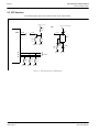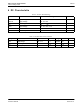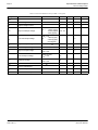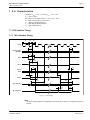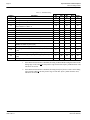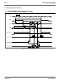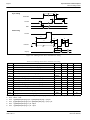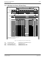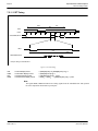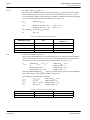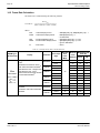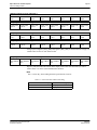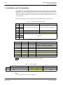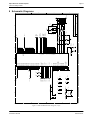
1
SED1355 Embedded RAMDAC LCD/CRT Controller SED1355 TECHNICAL MANUAL Document Number: X23A-Q-001-09 Copyright © 1998, 1999 Epson Research and Development, Inc. All Rights Reserved. Information in this document is subject to change without notice. You may download and use this document, but only for your own use in evaluating Seiko Epson/EPSON products. You may not modify the document. Epson Research and Development, Inc. disclaims any representation that the contents of this document are accurate or current. The Programs/Technologies described in this document may contain material protected under U.S. and/or International Patent laws. EPSON is a registered trademark of Seiko Epson Corporation. All other trademarks are the property of their respective owners. Page 2 Epson Research and Development Vancouver Design Center THIS PAGE LEFT BLANK SED1355 X23A-Q-001-09 TECHNICAL MANUAL Issue Date: 99/10/06 Epson Research and Development Vancouver Design Center Page 3 Customer Support Information Comprehensive Support Tools Seiko Epson Corp. provides to the system designer and computer OEM manufacturer a complete set of resources and tools for the development of graphics systems. Evaluation / Demonstration Board • Assembled and fully tested graphics evaluation board with installation guide and schematics. • To borrow an evaluation board, please contact your local Seiko Epson Corp. sales representative. Chip Documentation • Technical manual includes Data Sheet, Application Notes, and Programmer’s Reference. Software • OEM Utilities. • User Utilities. • Evaluation Software. • To obtain these programs, contact Application Engineering Support. Application Engineering Support Engineering and Sales Support is provided by: Japan Seiko Epson Corporation Electronic Devices Marketing Division 421-8, Hino, Hino-shi Tokyo 191-8501, Japan Tel: 042-587-5812 Fax: 042-587-5564 http://www.epson.co.jp Hong Kong Epson Hong Kong Ltd. 20/F., Harbour Centre 25 Harbour Road Wanchai, Hong Kong Tel: 2585-4600 Fax: 2827-4346 TECHNICAL MANUAL Issue Date: 99/10/06 North America Epson Electronics America, Inc. 150 River Oaks Parkway San Jose, CA 95134, USA Tel: (408) 922-0200 Fax: (408) 922-0238 http://www.eea.epson.com Taiwan, R.O.C. Epson Taiwan Technology & Trading Ltd. 10F, No. 287 Nanking East Road Sec. 3, Taipei, Taiwan, R.O.C. Tel: 02-2717-7360 Fax: 02-2712-9164 Europe Epson Europe Electronics GmbH Riesstrasse 15 80992 Munich, Germany Tel: 089-14005-0 Fax: 089-14005-110 Singapore Epson Singapore Pte., Ltd. No. 1 Temasek Avenue #36-00 Millenia Tower Singapore, 039192 Tel: 337-7911 Fax: 334-2716 SED1355 X23A-Q-001-09 Page 4 Epson Research and Development Vancouver Design Center THIS PAGE LEFT BLANK SED1355 X23A-Q-001-09 TECHNICAL MANUAL Issue Date: 99/10/06 Epson Research and Development Vancouver Design Center Page 5 Table of Contents INTRODUCTION SED1355 Embedded RAMDAC LCD/CRT Controller Product Brief SPECIFICATION SED1355 Hardware Functional Specification PROGRAMMER’S REFERENCE SED1355 Programming Notes and Examples SED1355 Register Summary UTILITIES 1355CFG Configuration Program 1355SHOW Demonstration Program 1355SPLT Display Utility 1355VIRT Display Utility 1355PLAY Diagnostic Utility 1355BMP Demonstration Program 1355PWR Software Suspend Power Sequencing Utility DRIVERS SED1355 Windows® CE Display Drivers EVALUATION SDU1355B0C Rev. 1.0 ISA Bus Evaluation Board User Manual SDU1355-D9000 Evaluation Board User Guide APPLICATION NOTES Power Consumption Interfacing to the Philips MIPS PR31500/PR31700 Processor Interfacing to the PC Card Bus Interfacing to the NEC VR4102/VR4111™ Microprocessor Interfacing to the Motorola MPC821 Microprocessor Interfacing to the NEC VR4121™ Microprocessor Interfacing to the Toshiba MIPS TX3912 Processor Interfacing to the NEC V832 Microprocessor TECHNICAL MANUAL Issue Date: 99/10/06 SED1355 X23A-Q-001-09 Page 6 Epson Research and Development Vancouver Design Center THIS PAGE LEFT BLANK SED1355 X23A-Q-001-09 TECHNICAL MANUAL Issue Date: 99/10/06 ENERGY S AV I N G GRAPHICS EPSON SED1355 SED1355 EMBEDDED RAMDAC LCD/CRT CONTROLLER October 1998 ■ DESCRIPTION The SED1355 is a color/monochrome LCD/CRT graphics controller interfacing to a wide range of CPUs and display devices. The SED1355 architecture is designed to meet the low cost, low power requirements of the embedded markets, such as Mobile Communications, Hand-Held PCs, and Office Automation. The SED1355 supports multiple CPUs, all LCD panel types, CRT, and additionally provides a number of differentiating features. Products requiring a “Portrait” mode display can take advantage of the Hardware Portrait Mode feature. Simultaneous, Virtual and Split Screen Display are just some of the display modes supported, while the Hardware Cursor, Ink Layer, and the Memory Enhancement Registers offer substantial performance benefits. These features, combined with the SED1355’s Operating System independence, make it an ideal display solution for a wide variety of applications. ■ FEATURES Memory Interface • 16-bit EDO-DRAM or FPM-DRAM interface. • Memory size options: 512K bytes using one 256K×16 device. 2M bytes using one 1M×16 device. • Addressable as a single linear address space. CPU Interface • Supports the following interfaces: Hitachi SH-4. Hitachi SH-3. Motorola M68K. Philips MIPS PR31500/PR31700. Toshiba MIPS TX3912. Motorola Power PC MPC821. NEC MIPS VR4102/VR4111. Epson E0C33. PC Card (PCMCIA). StrongARM (PC Card). ISA bus. MPU bus interface with programmable READY. • CPU write buffer. Display Support • 4/8-bit monochrome passive LCD interface. • 4/8/16-bit color passive LCD interface. • Single-panel, single-drive displays. • Dual-panel, dual-drive displays. • Direct support for 9/12-bit TFT/D-TFD; 18-bit TFT/D-TFD is supported up to 64K color depth (16-bit data). • Embedded RAMDAC with direct analog CRT drive. • Simultaneous display of CRT and passive or TFT/D-TFD panels. • Maximum resolution of 800x600 pixels at a color depth of 16 bpp. X23A-C-002-13 Display Modes • 1/2/4/8/16 bit-per-pixel (bpp) support on LCD/CRT. • Up to 16 shades of gray using FRM on monochrome passive LCD panels. • Up to 4096 colors on passive LCD panels. • Up to 64K colors on active matrix TFT/D-TFD LCD panels and CRT in 16 bpp modes. • Split Screen Display: allows two different images to be simultaneously viewed on the same display. • Virtual Display Support: displays images larger than the display size through the use of panning. • Double Buffering/multi-pages: provides smooth animation and instantaneous screen update. • Hardware Portrait Mode: direct hardware 90° rotation of display image for portrait mode display. • Acceleration of screen updates by allocating full display memory bandwidth to CPU. • Hardware 64x64 pixel 2-bit cursor or full screen 2-bit ink layer. Clock Source • Single clock input for both pixel and memory clocks. • Memory clock can be input clock or (input clock/2), providing flexibility to use CPU bus clock as input. • Pixel clock can be memory clock or (memory clock/2) or (memory clock/3) or (memory clock/4). Power Down Modes • Software power save mode. • LCD power sequencing. General Purpose IO Pins • Up to 3 General Purpose IO pins are available. Operating Voltage • 2.7 volts to 5.5 volts. Package • 128-pin QFP15 surface mount package. 1 GRAPHICS SED1355 ■ SYSTEM BLOCK DIAGRAM EDO-DRAM FPM-DRAM Analog Out CPU Data and Control Signals SED1355 CRT Digital Out Actual Size Flat Panel CONTACT YOUR SALES REPRESENTATIVE FOR THESE COMPREHENSIVE DESIGN TOOLS: • SED1355 Technical Manual • SDU1355 Evaluation Boards • Windows CE Display Driver • CPU Independent Software Utilities Japan Seiko Epson Corporation Electronic Devices Marketing Division 421-8, Hino, Hino-shi Tokyo 191-8501, Japan Tel: 042-587-5812 Fax: 042-587-5564 http://www.epson.co.jp Hong Kong Epson Hong Kong Ltd. 20/F., Harbour Centre 25 Harbour Road Wanchai, Hong Kong Tel: 2585-4600 Fax: 2827-4346 FOR SYSTEM INTEGRATION SERVICES FOR WINDOWS® CE CONTACT: Epson Research & Development, Inc. Suite #320 - 11120 Horseshoe Way Richmond, B.C., Canada V7A 5H7 Tel: (604) 275-5151 Fax: (604) 275-2167 Email: [email protected] http://www.erd.epson.com North America Epson Electronics America, Inc. 150 River Oaks Parkway San Jose, CA 95134, USA Tel: (408) 922-0200 Fax: (408) 922-0238 http://www.eea.epson.com Taiwan, R.O.C. Epson Taiwan Technology & Trading Ltd. 10F, No. 287 Nanking East Road Sec. 3, Taipei, Taiwan, R.O.C. Tel: 02-2717-7360 Fax: 02-2712-9164 Europe Epson Europe Electronics GmbH Riesstrasse 15 80992 Munich, Germany Tel: 089-14005-0 Fax: 089-14005-110 Singapore Epson Singapore Pte., Ltd. No. 1 Temasek Avenue #36-00 Millenia Tower Singapore, 039192 Tel: 337-7911 Fax: 334-2716 Copyright © 1998 Epson Research and Development, Inc. All Rights Reserved. VDC Information in this document is subject to change without notice. You may download and use this document, but only for your own use in evaluating Seiko Epson/ EPSON products. You may not modify the document. Epson Research and Development, Inc. disclaims any representation that the contents of this document are accurate or current. The Programs/Technologies described in this document may contain material protected under U.S. and/or International Patent laws. EPSON is a registered trademark of Seiko Epson Corporation. Microsoft, Windows, and the Windows CE Logo are registered trademarks of Microsoft Corporation. 2 X23A-C-002-13 SED1355 Embedded RAMDAC LCD/CRT Controller Hardware Functional Specification Document Number: X23A-A-001-11 Copyright © 1998, 1999 Epson Research and Development, Inc. All Rights Reserved. Information in this document is subject to change without notice. You may download and use this document, but only for your own use in evaluating Seiko Epson/EPSON products. You may not modify the document. Epson Research and Development, Inc. disclaims any representation that the contents of this document are accurate or current. The Programs/Technologies described in this document may contain material protected under U.S. and/or International Patent laws. EPSON is a registered trademark of Seiko Epson Corporation. All other trademarks are the property of their respective owners. Page 2 Epson Research and Development Vancouver Design Center THIS PAGE LEFT BLANK SED1355 X23A-A-001-11 Hardware Functional Specification Issue Date: 99/05/18 Epson Research and Development Vancouver Design Center Page 3 Table of Contents 1 2 Introduction . . . . . . . . . . . . . . . . . . . . . . . . . . . . . . . . . . . . . . . . . . . . 11 1.1 Scope . . . . . . . . . . . . . . . . . . . . . . . . . . . . . . . . . . . . . 11 1.2 Overview Description . . . . . . . . . . . . . . . . . . . . . . . . . . . . . . . 11 Features . . . . . . . . . . . . . . . . . . . . . . . . . . . . . . . . . . . . . . . . . . . . . . 12 2.1 Memory Interface . . . . . . . . . . . . . . . . . . . . . . . . . . . . . . . . . 12 2.2 CPU Interface . . . . . . . . . . . . . . . . . . . . . . . . . . . . . . . . . . 12 2.3 Display Support 2.4 Display Modes . . . . . . . . . . . . . . . . . . . . . . . . . . . . . . . . . . 13 2.5 Display Features . . . . . . . . . . . . . . . . . . . . . . . . . . . . . . . . . 13 2.6 Clock Source 2.7 Miscellaneous . . . . . . . . . . . . . . . . . . . . . . . . . . . . . . . . . . 14 . . . . . . . . . . . . . . . . . . . . . . . . . . . . . . . . . 13 . . . . . . . . . . . . . . . . . . . . . . . . . . . . . . . . . . 13 3 Typical System Implementation Diagrams . . . . . . . . . . . . . . . . . . . . . . . . . . . 15 4 Internal Description 4.1 4.2 5 6 . . . . . . . . . . . . . . . . . . . . . . . . . . . . . . . . . . . . . . . 20 Block Diagram Showing Datapaths . . . . . . . . . . . . . . . . . . . . . . . . . . 20 Block Descriptions . . . . . . . . . . . . . . . . . . . . . . . . . . . . . . . . 20 4.2.1 Register . . . . . . . . . . . . . . . . . . . . . . . . . . . . . . . . . . . . . . . . . . . . . 20 4.2.2 Host Interface . . . . . . . . . . . . . . . . . . . . . . . . . . . . . . . . . . . . . . . . . . 20 4.2.3 CPU R/W . . . . . . . . . . . . . . . . . . . . . . . . . . . . . . . . . . . . . . . . . . . . 20 4.2.4 Memory Controller . . . . . . . . . . . . . . . . . . . . . . . . . . . . . . . . . . . . . . . 21 4.2.5 Display FIFO . . . . . . . . . . . . . . . . . . . . . . . . . . . . . . . . . . . . . . . . . . 21 4.2.6 Cursor FIFO . . . . . . . . . . . . . . . . . . . . . . . . . . . . . . . . . . . . . . . . . . . 21 4.2.7 Look-Up Tables . . . . . . . . . . . . . . . . . . . . . . . . . . . . . . . . . . . . . . . . . 21 4.2.8 CRTC . . . . . . . . . . . . . . . . . . . . . . . . . . . . . . . . . . . . . . . . . . . . . . 21 4.2.9 LCD Interface . . . . . . . . . . . . . . . . . . . . . . . . . . . . . . . . . . . . . . . . . . 21 4.2.10 DAC . . . . . . . . . . . . . . . . . . . . . . . . . . . . . . . . . . . . . . . . . . . . . . . 21 4.2.11 Power Save . . . . . . . . . . . . . . . . . . . . . . . . . . . . . . . . . . . . . . . . . . . 21 4.2.12 Clocks . . . . . . . . . . . . . . . . . . . . . . . . . . . . . . . . . . . . . . . . . . . . . . 21 Pins . . . . . . . . . . . . . . . . . . . . . . . . . . . . . . . . . . . . . . . . . . . . . . . . 22 5.1 Pinout Diagram . . . . . . . . . . . . . . . . . . . . . . . . . . . . . . . . . . 22 5.2 Pin Description . . . . . . . . . . . . . . . . . . . . . . . . . . . . . . . . . . 23 5.2.1 Host Interface . . . . . . . . . . . . . . . . . . . . . . . . . . . . . . . . . . . . . . . . . . 23 5.2.2 Memory Interface . . . . . . . . . . . . . . . . . . . . . . . . . . . . . . . . . . . . . . . . 29 5.2.3 LCD Interface . . . . . . . . . . . . . . . . . . . . . . . . . . . . . . . . . . . . . . . . . . 31 5.2.4 CRT Interface . . . . . . . . . . . . . . . . . . . . . . . . . . . . . . . . . . . . . . . . . . 31 5.2.5 Miscellaneous . . . . . . . . . . . . . . . . . . . . . . . . . . . . . . . . . . . . . . . . . . 32 5.3 Summary of Configuration Options . . . . . . . . . . . . . . . . . . . . . . . . . . 33 5.4 Multiple Function Pin Mapping . . . . . . . . . . . . . . . . . . . . . . . . . . . 34 5.5 CRT Interface . . . . . . . . . . . . . . . . . . . . . . . . . . . . . . . . . . 36 D.C. Characteristics . . . . . . . . . . . . . . . . . . . . . . . . . . . . . . . . . . . . . . . 37 Hardware Functional Specification Issue Date: 99/05/18 SED1355 X23A-A-001-11 Page 4 7 Epson Research and Development Vancouver Design Center A.C. Characteristics 7.1 CPU Interface Timing . . . . . . . . . . . . . . . . . . . . . . . . . . . . . . . 41 7.1.1 SH-4 Interface Timing . . . . . . . . . . . . . . . . . . . . . . . . . . . . . . . . . . . . . .41 7.1.2 SH-3 Interface Timing . . . . . . . . . . . . . . . . . . . . . . . . . . . . . . . . . . . . . .43 7.1.3 MC68K Bus 1 Interface Timing (e.g. MC68000) . . . . . . . . . . . . . . . . . . . . . . . .45 7.1.4 MC68K Bus 2 Interface Timing (e.g. MC68030) . . . . . . . . . . . . . . . . . . . . . . . .47 7.1.5 PC Card Interface Timing . . . . . . . . . . . . . . . . . . . . . . . . . . . . . . . . . . . .49 7.1.6 Generic Interface Timing . . . . . . . . . . . . . . . . . . . . . . . . . . . . . . . . . . . . .51 7.1.7 MIPS/ISA Interface Timing . . . . . . . . . . . . . . . . . . . . . . . . . . . . . . . . . . .53 7.1.8 Philips Interface Timing (e.g. PR31500/PR31700) . . . . . . . . . . . . . . . . . . . . . . .55 7.1.9 Toshiba Interface Timing (e.g. TX3912) . . . . . . . . . . . . . . . . . . . . . . . . . . . . .58 7.1.10 Power PC Interface Timing (e.g. MPC8xx, MC68040, Coldfire) . . . . . . . . . . . . . . . .61 7.2 Clock Input Requirements . . . . . . . . . . . . . . . . . . . . . . . . . . . . . 63 7.3 Memory Interface Timing . . . . . . . . . . . . . . . . . . . . . . . . . . . . . 64 7.3.1 EDO-DRAM Read/Write/Read-Write Timing . . . . . . . . . . . . . . . . . . . . . . . . . .64 7.3.2 EDO-DRAM CAS Before RAS Refresh Timing . . . . . . . . . . . . . . . . . . . . . . . .67 7.3.3 EDO-DRAM Self-Refresh Timing . . . . . . . . . . . . . . . . . . . . . . . . . . . . . . . .69 7.3.4 FPM-DRAM Read/Write/Read-Write Timing . . . . . . . . . . . . . . . . . . . . . . . . . .70 7.3.5 FPM-DRAM CAS Before RAS Refresh Timing . . . . . . . . . . . . . . . . . . . . . . . .73 7.3.6 FPM-DRAM Self-Refresh Timing . . . . . . . . . . . . . . . . . . . . . . . . . . . . . . . .74 7.4 Power Sequencing . . . . . . . . . . . . . . . . . . . . . . . . . . . . . . . . 75 7.4.1 LCD Power Sequencing . . . . . . . . . . . . . . . . . . . . . . . . . . . . . . . . . . . . .75 7.4.2 Power Save Status . . . . . . . . . . . . . . . . . . . . . . . . . . . . . . . . . . . . . . . .76 7.5 8 . . . . . . . . . . . . . . . . . . . . . . . . . . . . . . . . . . . . . . . 41 Display Interface . . . . . . . . . . . . . . . . . . . . . . . . . . . . . . . . . 77 7.5.1 4-Bit Single Monochrome Passive LCD Panel Timing . . . . . . . . . . . . . . . . . . . . .77 7.5.2 8-Bit Single Monochrome Passive LCD Panel Timing . . . . . . . . . . . . . . . . . . . . .79 7.5.3 4-Bit Single Color Passive LCD Panel Timing . . . . . . . . . . . . . . . . . . . . . . . . .81 7.5.4 8-Bit Single Color Passive LCD Panel Timing (Format 1) . . . . . . . . . . . . . . . . . . .83 7.5.5 8-Bit Single Color Passive LCD Panel Timing (Format 2) . . . . . . . . . . . . . . . . . . .85 7.5.6 16-Bit Single Color Passive LCD Panel Timing . . . . . . . . . . . . . . . . . . . . . . . . .87 7.5.7 8-Bit Dual Monochrome Passive LCD Panel Timing . . . . . . . . . . . . . . . . . . . . . .89 7.5.8 8-Bit Dual Color Passive LCD Panel Timing . . . . . . . . . . . . . . . . . . . . . . . . . .91 7.5.9 16-Bit Dual Color Passive LCD Panel Timing . . . . . . . . . . . . . . . . . . . . . . . . . .93 7.5.10 16-Bit TFT/D-TFD Panel Timing . . . . . . . . . . . . . . . . . . . . . . . . . . . . . . . .95 7.5.11 CRT Timing . . . . . . . . . . . . . . . . . . . . . . . . . . . . . . . . . . . . . . . . . . .98 Registers . . . . . . . . . . . . . . . . . . . . . . . . . . . . . . . . . . . . . . . . . . . . 100 8.1 Register Mapping 8.2 Register Descriptions . . . . . . . . . . . . . . . . . . . . . . . . . . . . . . . 100 . . . . . . . . . . . . . . . . . . . . . . . . . . . . . . . . 100 8.2.1 Revision Code Register . . . . . . . . . . . . . . . . . . . . . . . . . . . . . . . . . . . . 100 8.2.2 Memory Configuration Registers . . . . . . . . . . . . . . . . . . . . . . . . . . . . . . . 101 8.2.3 Panel/Monitor Configuration Registers . . . . . . . . . . . . . . . . . . . . . . . . . . . . 102 8.2.4 Display Configuration Registers . . . . . . . . . . . . . . . . . . . . . . . . . . . . . . . . 107 SED1355 X23A-A-001-11 Hardware Functional Specification Issue Date: 99/05/18 Epson Research and Development Vancouver Design Center 9 Page 5 8.2.5 Clock Configuration Register . . . . . . . . . . . . . . . . . . . . . . . . . . . . . . . . . 111 8.2.6 Power Save Configuration Registers . . . . . . . . . . . . . . . . . . . . . . . . . . . . . 112 8.2.7 Miscellaneous Registers . . . . . . . . . . . . . . . . . . . . . . . . . . . . . . . . . . . . 113 8.2.8 Look-Up Table Registers . . . . . . . . . . . . . . . . . . . . . . . . . . . . . . . . . . . 118 8.2.9 Ink/Cursor Registers . . . . . . . . . . . . . . . . . . . . . . . . . . . . . . . . . . . . . . 120 Display Buffer . . . . . . . . . . . . . . . . . . . . . . . . . . . . . . . . . . . . . . . . . . .123 9.1 Image Buffer . . . . . . . . . . . . . . . . . . . . . . . . . . . . . . . . . . .124 9.2 Ink/Cursor Buffers . . . . . . . . . . . . . . . . . . . . . . . . . . . . . . . .124 9.3 Half Frame Buffer . . . . . . . . . . . . . . . . . . . . . . . . . . . . . . . .124 10 Display Configuration . . . . . . . . . . . . . . . . . . . . . . . . . . . . . . . . . . . . . .125 10.1 Display Mode Data Format . . . . . . . . . . . . . . . . . . . . . . . . . . . . .125 10.2 Image Manipulation . . . . . . . . . . . . . . . . . . . . . . . . . . . . . . . .127 11 Look-Up Table Architecture . . . . . . . . . . . . . . . . . . . . . . . . . . . . . . . . . . .128 11.1 Monochrome Modes . . . . . . . . . . . . . . . . . . . . . . . . . . . . . . . .128 11.2 Color Modes . . . . . . . . . . . . . . . . . . . . . . . . . . . . . . . . . . .130 12 Ink/Cursor Architecture . . . . . . . . . . . . . . . . . . . . . . . . . . . . . . . . . . . . .134 12.1 Ink/Cursor Buffers . . . . . . . . . . . . . . . . . . . . . . . . . . . . . . . .134 12.2 Ink/Cursor Data Format . . . . . . . . . . . . . . . . . . . . . . . . . . . . . .134 12.3 Ink/Cursor Image Manipulation . . . . . . . . . . . . . . . . . . . . . . . . . . .135 12.3.1 Ink Image . . . . . . . . . . . . . . . . . . . . . . . . . . . . . . . . . . . . . . . . . . . 135 12.3.2 Cursor Image . . . . . . . . . . . . . . . . . . . . . . . . . . . . . . . . . . . . . . . . . 135 13 SwivelView™ . . . . . . . . . . . . . . . . . . . . . . . . . . . . . . . . . . . . . . . . . . .136 13.1 Concept . . . . . . . . . . . . . . . . . . . . . . . . . . . . . . . . . . . . .136 13.2 Image Manipulation in SwivelView . . . . . . . . . . . . . . . . . . . . . . . . . .137 13.3 Physical Memory Requirement 13.4 Limitations . . . . . . . . . . . . . . . . . . . . . . . . . . .138 . . . . . . . . . . . . . . . . . . . . . . . . . . . . . . . . . . .139 14 Clocking . . . . . . . . . . . . . . . . . . . . . . . . . . . . . . . . . . . . . . . . . . . . . .140 14.1 Maximum MCLK: PCLK Ratios . . . . . . . . . . . . . . . . . . . . . . . . . . .140 14.2 Frame Rate Calculation . . . . . . . . . . . . . . . . . . . . . . . . . . . . . .142 14.3 Bandwidth Calculation . . . . . . . . . . . . . . . . . . . . . . . . . . . . . . .144 15 Power Save Modes . . . . . . . . . . . . . . . . . . . . . . . . . . . . . . . . . . . . . . . .148 16 Mechanical Data . . . . . . . . . . . . . . . . . . . . . . . . . . . . . . . . . . . . . . . . .149 Hardware Functional Specification Issue Date: 99/05/18 SED1355 X23A-A-001-11 Page 6 Epson Research and Development Vancouver Design Center THIS PAGE LEFT BLANK SED1355 X23A-A-001-11 Hardware Functional Specification Issue Date: 99/05/18 Epson Research and Development Vancouver Design Center Page 7 List of Tables Table 5-1: Host Interface Pin Descriptions . . . . . . . . . . . . . . . . . . . . . . . . . . . . . . . . . . . . 23 Table 5-2: Memory Interface Pin Descriptions . . . . . . . . . . . . . . . . . . . . . . . . . . . . . . . . . . 29 Table 5-2: LCD Interface Pin Descriptions. . . . . . . . . . . . . . . . . . . . . . . . . . . . . . . . . . . . 31 Table 5-3: CRT Interface Pin Descriptions . . . . . . . . . . . . . . . . . . . . . . . . . . . . . . . . . . . . 31 Table 5-4: Miscellaneous Interface Pin Descriptions. . . . . . . . . . . . . . . . . . . . . . . . . . . . . . . 32 Table 5-5: Summary of Power On/Reset Options . . . . . . . . . . . . . . . . . . . . . . . . . . . . . . . . 33 Table 5-6: CPU Interface Pin Mapping. . . . . . . . . . . . . . . . . . . . . . . . . . . . . . . . . . . . . . 34 Table 5-7: Memory Interface Pin Mapping. . . . . . . . . . . . . . . . . . . . . . . . . . . . . . . . . . . . 35 Table 5-8: LCD Interface Pin Mapping . . . . . . . . . . . . . . . . . . . . . . . . . . . . . . . . . . . . . 35 Table 6-1: Absolute Maximum Ratings . . . . . . . . . . . . . . . . . . . . . . . . . . . . . . . . . . . . . 37 Table 6-2: Recommended Operating Conditions . . . . . . . . . . . . . . . . . . . . . . . . . . . . . . . . . 37 Table 6-3: Electrical Characteristics for VDD = 5.0V typical . . . . . . . . . . . . . . . . . . . . . . . . . . 38 Table 6-4: Electrical Characteristics for VDD = 3.3V typical . . . . . . . . . . . . . . . . . . . . . . . . . . 39 Table 6-5: Electrical Characteristics for VDD = 3.0V typical . . . . . . . . . . . . . . . . . . . . . . . . . . 40 Table 7-1: SH-4 Timing . . . . . . . . . . . . . . . . . . . . . . . . . . . . . . . . . . . . . . . . . . . . . 42 Table 7-2: SH-3 Timing . . . . . . . . . . . . . . . . . . . . . . . . . . . . . . . . . . . . . . . . . . . . . 44 Table 7-3: MC68000 Timing . . . . . . . . . . . . . . . . . . . . . . . . . . . . . . . . . . . . . . . . . . . 46 Table 7-4: MC68030 Timing . . . . . . . . . . . . . . . . . . . . . . . . . . . . . . . . . . . . . . . . . . . 48 Table 7-5: PC Card Timing . . . . . . . . . . . . . . . . . . . . . . . . . . . . . . . . . . . . . . . . . . . . 50 Table 7-6: Generic Timing . . . . . . . . . . . . . . . . . . . . . . . . . . . . . . . . . . . . . . . . . . . . 52 Table 7-7: MIPS/ISA Timing. . . . . . . . . . . . . . . . . . . . . . . . . . . . . . . . . . . . . . . . . . . 54 Table 7-8: Philips Timing. . . . . . . . . . . . . . . . . . . . . . . . . . . . . . . . . . . . . . . . . . . . . 56 Table 7-9: Clock Input Requirements for BUSCLK using Philips local bus. . . . . . . . . . . . . . . . . . . 57 Table 7-10: Toshiba Timing . . . . . . . . . . . . . . . . . . . . . . . . . . . . . . . . . . . . . . . . . . . . 59 Table 7-11: Clock Input Requirements for BUSCLK using Toshiba local bus . . . . . . . . . . . . . . . . . . 60 Table 7-12: Power PC Timing . . . . . . . . . . . . . . . . . . . . . . . . . . . . . . . . . . . . . . . . . . . 62 Table 7-13: Clock Input Requirements for CLKI divided down internally (MCLK = CLKI/2) . . . . . . . . . 63 Table 7-14: Clock Input Requirements for CLKI . . . . . . . . . . . . . . . . . . . . . . . . . . . . . . . . . 63 Table 7-15: EDO-DRAM Read/Write/Read-Write Timing . . . . . . . . . . . . . . . . . . . . . . . . . . . . 65 Table 7-16: EDO-DRAM CAS Before RAS Refresh Timing . . . . . . . . . . . . . . . . . . . . . . . . . . . 67 Table 7-17: EDO-DRAM Self-Refresh Timing . . . . . . . . . . . . . . . . . . . . . . . . . . . . . . . . . . 69 Table 7-18: FPM-DRAM Read/Write/Read-Write Timing . . . . . . . . . . . . . . . . . . . . . . . . . . . . 71 Table 7-19: FPM-DRAM CAS Before RAS Refresh Timing . . . . . . . . . . . . . . . . . . . . . . . . . . . 73 Table 7-20: FPM-DRAM CBR Self-Refresh Timing . . . . . . . . . . . . . . . . . . . . . . . . . . . . . . . 74 Table 7-21: LCD Panel Power Off/ Power On. . . . . . . . . . . . . . . . . . . . . . . . . . . . . . . . . . . 75 Table 7-22: Power Save Status and Local Bus Memory Access Relative to Power Save Mode . . . . . . . . . 76 Table 7-23: 4-Bit Single Monochrome Passive LCD Panel A.C. Timing . . . . . . . . . . . . . . . . . . . . . 78 Table 7-24: 8-Bit Single Monochrome Passive LCD Panel A.C. Timing . . . . . . . . . . . . . . . . . . . . . 80 Table 7-25: 4-Bit Single Color Passive LCD Panel A.C. Timing . . . . . . . . . . . . . . . . . . . . . . . . . 82 Table 7-26: 8-Bit Single Color Passive LCD Panel A.C. Timing (Format 1) . . . . . . . . . . . . . . . . . . . 84 Hardware Functional Specification Issue Date: 99/05/18 SED1355 X23A-A-001-11 Page 8 Epson Research and Development Vancouver Design Center Table 7-27: 8-Bit Single Color Passive LCD Panel A.C. Timing (Format 2) . . . . . . . . . . . . . . . . . . .86 Table 7-28: 16-Bit Single Color Passive LCD Panel A.C. Timing. . . . . . . . . . . . . . . . . . . . . . . . .88 Table 7-29: 8-Bit Dual Monochrome Passive LCD Panel A.C. Timing . . . . . . . . . . . . . . . . . . . . . .90 Table 7-30: 8-Bit Dual Color Passive LCD Panel A.C. Timing . . . . . . . . . . . . . . . . . . . . . . . . . .92 Table 7-31: 16-Bit Dual Color Passive LCD Panel A.C. Timing . . . . . . . . . . . . . . . . . . . . . . . . .94 Table 7-32: TFT/D-TFD A.C. Timing . . . . . . . . . . . . . . . . . . . . . . . . . . . . . . . . . . . . . . .97 Table 8-1: SED1355 Addressing . . . . . . . . . . . . . . . . . . . . . . . . . . . . . . . . . . . . . . . . 100 Table 8-2: DRAM Refresh Rate Selection . . . . . . . . . . . . . . . . . . . . . . . . . . . . . . . . . . . 101 Table 8-3: Panel Data Width Selection . . . . . . . . . . . . . . . . . . . . . . . . . . . . . . . . . . . . . 102 Table 8-4: FPLINE Polarity Selection . . . . . . . . . . . . . . . . . . . . . . . . . . . . . . . . . . . . . 104 Table 8-5: FPFRAME Polarity Selection . . . . . . . . . . . . . . . . . . . . . . . . . . . . . . . . . . . . 106 Table 8-6: Simultaneous Display Option Selection . . . . . . . . . . . . . . . . . . . . . . . . . . . . . . . 107 Table 8-7: Bit-per-pixel Selection . . . . . . . . . . . . . . . . . . . . . . . . . . . . . . . . . . . . . . . . 108 Table 8-8: Pixel Panning Selection . . . . . . . . . . . . . . . . . . . . . . . . . . . . . . . . . . . . . . . 111 Table 8-9: PCLK Divide Selection . . . . . . . . . . . . . . . . . . . . . . . . . . . . . . . . . . . . . . . 112 Table 8-10: Suspend Refresh Selection. . . . . . . . . . . . . . . . . . . . . . . . . . . . . . . . . . . . . . 112 Table 8-11: MA/GPIO Pin Functionality . . . . . . . . . . . . . . . . . . . . . . . . . . . . . . . . . . . . . 114 Table 8-12: Minimum Memory Timing Selection . . . . . . . . . . . . . . . . . . . . . . . . . . . . . . . . 116 Table 8-13: RAS#-to-CAS# Delay Timing Select . . . . . . . . . . . . . . . . . . . . . . . . . . . . . . . . 116 Table 8-14: RAS Precharge Timing Select . . . . . . . . . . . . . . . . . . . . . . . . . . . . . . . . . . . . 117 Table 8-15: Optimal NRC, NRP, and NRCD values at maximum MCLK frequency . . . . . . . . . . . . . . 117 Table 8-16: Minimum Memory Timing Selection . . . . . . . . . . . . . . . . . . . . . . . . . . . . . . . . 118 Table 8-17: Ink/Cursor Selection . . . . . . . . . . . . . . . . . . . . . . . . . . . . . . . . . . . . . . . . . 120 Table 8-18: Ink/Cursor Start Address Encoding . . . . . . . . . . . . . . . . . . . . . . . . . . . . . . . . . 122 Table 8-19: Recommended Alternate FRM Scheme . . . . . . . . . . . . . . . . . . . . . . . . . . . . . . . 122 Table 9-1: SED1355 Addressing . . . . . . . . . . . . . . . . . . . . . . . . . . . . . . . . . . . . . . . . 123 Table 12-1: Ink/Cursor Start Address Encoding . . . . . . . . . . . . . . . . . . . . . . . . . . . . . . . . . 134 Table 12-2: Ink/Cursor Color Select . . . . . . . . . . . . . . . . . . . . . . . . . . . . . . . . . . . . . . . 135 Table 13-2 Minimum DRAM Size Required for SwivelView. . . . . . . . . . . . . . . . . . . . . . . . . . 139 Table 14-1: Maximum PCLK Frequency with EDO-DRAM . . . . . . . . . . . . . . . . . . . . . . . . . . 140 Table 14-2: Maximum PCLK Frequency with FPM-DRAM . . . . . . . . . . . . . . . . . . . . . . . . . . 141 Table 14-3: Example Frame Rates with Ink Disabled . . . . . . . . . . . . . . . . . . . . . . . . . . . . . . 142 Table 14-4: Number of MCLKs required for various memory access . . . . . . . . . . . . . . . . . . . . . . 144 Table 14-5: Total # MCLKs taken for Display refresh . . . . . . . . . . . . . . . . . . . . . . . . . . . . . . 145 Table 14-6: Theoretical Maximum Bandwidth M byte/sec, Cursor/Ink disabled . . . . . . . . . . . . . . . . 146 Table 15-1: Power Save Mode Function Summary . . . . . . . . . . . . . . . . . . . . . . . . . . . . . . . 148 Table 15-2: Pin States in Power-save Modes . . . . . . . . . . . . . . . . . . . . . . . . . . . . . . . . . . . 148 SED1355 X23A-A-001-11 Hardware Functional Specification Issue Date: 99/05/18 Epson Research and Development Vancouver Design Center Page 9 List of Figures Figure 3-1: Typical System Diagram (SH-4 Bus) . . . . . . . . . . . . . . . . . . . . . . . . . . . . . . . 15 Figure 3-2: Typical System Diagram (SH-3 Bus) . . . . . . . . . . . . . . . . . . . . . . . . . . . . . . . 15 Figure 3-3: Typical System Diagram (MC68K Bus 1, 16-Bit 68000) . . . . . . . . . . . . . . . . . . . . . 16 Figure 3-4: Typical System Diagram (MC68K Bus 2, 32-Bit 68030) . . . . . . . . . . . . . . . . . . . . . 16 Figure 3-5: Typical System Diagram (Generic Bus) . . . . . . . . . . . . . . . . . . . . . . . . . . . . . . 17 Figure 3-6: Typical System Diagram (NEC VR41xx (MIPS) Bus) . . . . . . . . . . . . . . . . . . . . . . 17 Figure 3-7: Typical System Diagram (Philips PR31500/PR31700 Bus) . . . . . . . . . . . . . . . . . . . . 18 Figure 3-8: Typical System Diagram (Toshiba TX3912 Bus) . . . . . . . . . . . . . . . . . . . . . . . . . 18 Figure 3-9: Typical System Diagram (Power PC Bus) . . . . . . . . . . . . . . . . . . . . . . . . . . . . . 19 Figure 3-10: Typical System Diagram (PC Card (PCMCIA) Bus) . . . . . . . . . . . . . . . . . . . . . . . 19 Figure 5-1: Pinout Diagram. . . . . . . . . . . . . . . . . . . . . . . . . . . . . . . . . . . . . . . . . . . 22 Figure 5-3: External Circuitry for CRT Interface . . . . . . . . . . . . . . . . . . . . . . . . . . . . . . . 36 Figure 7-1: SH-4 Timing . . . . . . . . . . . . . . . . . . . . . . . . . . . . . . . . . . . . . . . . . . . . 41 Figure 7-2: SH-3 Timing . . . . . . . . . . . . . . . . . . . . . . . . . . . . . . . . . . . . . . . . . . . . 43 Figure 7-3: MC68000 Timing . . . . . . . . . . . . . . . . . . . . . . . . . . . . . . . . . . . . . . . . . 45 Figure 7-4: MC68030 Timing . . . . . . . . . . . . . . . . . . . . . . . . . . . . . . . . . . . . . . . . . 47 Figure 7-5: PC Card Timing . . . . . . . . . . . . . . . . . . . . . . . . . . . . . . . . . . . . . . . . . . 49 Figure 7-6: Generic Timing. . . . . . . . . . . . . . . . . . . . . . . . . . . . . . . . . . . . . . . . . . . 51 Figure 7-7: MIPS/ISA Timing . . . . . . . . . . . . . . . . . . . . . . . . . . . . . . . . . . . . . . . . . 53 Figure 7-8: Philips Timing . . . . . . . . . . . . . . . . . . . . . . . . . . . . . . . . . . . . . . . . . . . 55 Figure 7-9: Clock Input Requirement . . . . . . . . . . . . . . . . . . . . . . . . . . . . . . . . . . . . . 57 Figure 7-10: Toshiba Timing . . . . . . . . . . . . . . . . . . . . . . . . . . . . . . . . . . . . . . . . . . 58 Figure 7-11: Clock Input Requirement . . . . . . . . . . . . . . . . . . . . . . . . . . . . . . . . . . . . . 60 Figure 7-12: Power PC Timing . . . . . . . . . . . . . . . . . . . . . . . . . . . . . . . . . . . . . . . . . 61 Figure 7-13: Clock Input Requirement . . . . . . . . . . . . . . . . . . . . . . . . . . . . . . . . . . . . . 63 Figure 7-14: EDO-DRAM Read/Write Timing . . . . . . . . . . . . . . . . . . . . . . . . . . . . . . . . . 64 Figure 7-15: EDO-DRAM Read-Write Timing . . . . . . . . . . . . . . . . . . . . . . . . . . . . . . . . . 65 Figure 7-16: EDO-DRAM CAS Before RAS Refresh Timing . . . . . . . . . . . . . . . . . . . . . . . . . 67 Figure 7-17: EDO-DRAM Self-Refresh Timing . . . . . . . . . . . . . . . . . . . . . . . . . . . . . . . . 69 Figure 7-18: FPM-DRAM Read/Write Timing . . . . . . . . . . . . . . . . . . . . . . . . . . . . . . . . . 70 Figure 7-19: FPM-DRAM Read-Write Timing . . . . . . . . . . . . . . . . . . . . . . . . . . . . . . . . . 71 Figure 7-20: FPM-DRAM CAS Before RAS Refresh Timing . . . . . . . . . . . . . . . . . . . . . . . . . 73 Figure 7-21: FPM-DRAM Self-Refresh Timing. . . . . . . . . . . . . . . . . . . . . . . . . . . . . . . . . 74 Figure 7-22: LCD Panel Power Off / Power On Timing. Drawn with LCDPWR set to active high polarity . . 75 Figure 7-23: Power Save Status and Local Bus Memory Access Relative to Power Save Mode . . . . . . . . 76 Figure 7-24: 4-Bit Single Monochrome Passive LCD Panel Timing . . . . . . . . . . . . . . . . . . . . . . 7 7 Figure 7-25: 4-Bit Single Monochrome Passive LCD Panel A.C. Timing . . . . . . . . . . . . . . . . . . . 78 Figure 7-26: 8-Bit Single Monochrome Passive LCD Panel Timing . . . . . . . . . . . . . . . . . . . . . . 7 9 Figure 7-27: 8-Bit Single Monochrome Passive LCD Panel A.C. Timing . . . . . . . . . . . . . . . . . . . 80 Figure 7-28: 4-Bit Single Color Passive LCD Panel Timing . . . . . . . . . . . . . . . . . . . . . . . . . . 81 Figure 7-29: 4-Bit Single Color Passive LCD Panel A.C. Timing . . . . . . . . . . . . . . . . . . . . . . . 82 Hardware Functional Specification Issue Date: 99/05/18 SED1355 X23A-A-001-11 Page 10 Epson Research and Development Vancouver Design Center Figure 7-30: 8-Bit Single Color Passive LCD Panel Timing (Format 1). . . . . . . . . . . . . . . . . . . . . 83 Figure 7-31: 8-Bit Single Color Passive LCD Panel A.C. Timing (Format 1) . . . . . . . . . . . . . . . . . . 84 Figure 7-32: 8-Bit Single Color Passive LCD Panel Timing (Format 2). . . . . . . . . . . . . . . . . . . . . 85 Figure 7-33: 8-Bit Single Color Passive LCD Panel A.C. Timing (Format 2) . . . . . . . . . . . . . . . . . . 86 Figure 7-34: 16-Bit Single Color Passive LCD Panel Timing . . . . . . . . . . . . . . . . . . . . . . . . . . 87 Figure 7-35: 16-Bit Single Color Passive LCD Panel A.C. Timing . . . . . . . . . . . . . . . . . . . . . . . 88 Figure 7-36: 8-Bit Dual Monochrome Passive LCD Panel Timing . . . . . . . . . . . . . . . . . . . . . . . 89 Figure 7-37: 8-Bit Dual Monochrome Passive LCD Panel A.C. Timing . . . . . . . . . . . . . . . . . . . . 90 Figure 7-38: 8-Bit Dual Color Passive LCD Panel Timing . . . . . . . . . . . . . . . . . . . . . . . . . . . 91 Figure 7-39: 8-Bit Dual Color Passive LCD Panel A.C. Timing. . . . . . . . . . . . . . . . . . . . . . . . . 92 Figure 7-40: 16-Bit Dual Color Passive LCD Panel Timing . . . . . . . . . . . . . . . . . . . . . . . . . . . 93 Figure 7-41: 16-Bit Dual Color Passive LCD Panel A.C. Timing . . . . . . . . . . . . . . . . . . . . . . . . 94 Figure 7-42: 16-Bit TFT/D-TFD Panel Timing . . . . . . . . . . . . . . . . . . . . . . . . . . . . . . . . . 95 Figure 7-43: TFT/D-TFD A.C. Timing. . . . . . . . . . . . . . . . . . . . . . . . . . . . . . . . . . . . . . 96 Figure 7-44: CRT Timing. . . . . . . . . . . . . . . . . . . . . . . . . . . . . . . . . . . . . . . . . . . . . 98 Figure 7-45: CRT A.C. Timing . . . . . . . . . . . . . . . . . . . . . . . . . . . . . . . . . . . . . . . . . . 99 Figure 9-1: Display Buffer Addressing . . . . . . . . . . . . . . . . . . . . . . . . . . . . . . . . . . . . 123 Figure 10-1: 1/2/4/8 Bit-per-pixel Format Memory Organization . . . . . . . . . . . . . . . . . . . . . . . 125 Figure 10-2: 15/16 Bit-per-pixel Format Memory Organization . . . . . . . . . . . . . . . . . . . . . . . . 126 Figure 10-3: Image Manipulation. . . . . . . . . . . . . . . . . . . . . . . . . . . . . . . . . . . . . . . . 127 Figure 11-1: 1 Bit-per-pixel Monochrome Mode Data Output Path . . . . . . . . . . . . . . . . . . . . . . 128 Figure 11-2: 2 Bit-per-pixel Monochrome Mode Data Output Path . . . . . . . . . . . . . . . . . . . . . . 128 Figure 11-3: 4 Bit-per-pixel Monochrome Mode Data Output Path . . . . . . . . . . . . . . . . . . . . . . 129 Figure 11-4: 1 Bit-per-pixel Color Mode Data Output Path . . . . . . . . . . . . . . . . . . . . . . . . . . 130 Figure 11-5: 2 Bit-per-pixel Color Mode Data Output Path . . . . . . . . . . . . . . . . . . . . . . . . . . 131 Figure 11-6: 4 Bit-per-pixel Color Mode Data Output Path . . . . . . . . . . . . . . . . . . . . . . . . . . 132 Figure 11-7: 8 Bit-per-pixel Color Mode Data Output Path . . . . . . . . . . . . . . . . . . . . . . . . . . 133 Figure 12-1: Ink/Cursor Data Format. . . . . . . . . . . . . . . . . . . . . . . . . . . . . . . . . . . . . . 134 Figure 12-2: Cursor Positioning . . . . . . . . . . . . . . . . . . . . . . . . . . . . . . . . . . . . . . . . 135 Figure 13-1: Relationship Between The Screen Image and the Image Residing in the Display Buffer . . . . 136 Figure 16-1: Mechanical Drawing QFP15 . . . . . . . . . . . . . . . . . . . . . . . . . . . . . . . . . . . 149 SED1355 X23A-A-001-11 Hardware Functional Specification Issue Date: 99/05/18 Epson Research and Development Vancouver Design Center Page 11 1 Introduction 1.1 Scope This is the Hardware Functional Specification for the SED1355 Embedded RAMDAC LCD/CRT Controller. Included in this document are timing diagrams, AC and DC characteristics, register descriptions, and power management descriptions. This document is intended for two audiences: Video Subsystem Designers and Software Developers. This specification will be updated as appropriate. Please check the Epson Electronics America Website at http://www.eea.epson.com for the latest revision of this document before beginning any development. We appreciate your comments on our documentation. Please contact us via email at [email protected]. 1.2 Overview Description The SED1355 is a color/monochrome LCD/CRT graphics controller interfacing to a wide range of CPUs and display devices. The SED1355 architecture is designed to meet the low cost, low power requirements of the embedded markets, such as Mobile Communications, Hand-Held PCs, and Office Automation. The SED1355 supports multiple CPUs, all LCD panel types, CRT, and additionally provides a number of differentiating features. Products requiring a “Portrait” mode display can take advantage of the SwivelView™ feature. Simultaneous, Virtual and Split Screen Display are just some of the display modes supported, while the Hardware Cursor, Ink Layer, and the Memory Enhancement Registers offer substantial performance benefits. These features, combined with the SED1355’s Operating System independence, make it an ideal display solution for a wide variety of applications. Hardware Functional Specification Issue Date: 99/05/18 SED1355 X23A-A-001-11 Page 12 Epson Research and Development Vancouver Design Center 2 Features 2.1 Memory Interface • 16-bit DRAM interface: • EDO-DRAM up to 40MHz data rate (80M bytes/sec.). • FPM-DRAM up to 25MHz data rate (50M bytes/sec.). • Memory size options: • 512K bytes using one 256K×16 device. • 2M bytes using one 1M×16 device. • Performance Enhancement Register to tailor the memory control output timing for the DRAM device. 2.2 CPU Interface • Supports the following interfaces: • 8/16-bit SH-4 bus interface. • 8/16-bit SH-3 bus interface. • 8/16-bit interface to 8/16/32-bit MC68000 microprocessors/microcontrollers. • 8/16-bit interface to 8/16/32-bit MC68030 microprocessors/microcontrollers. • Philips PR31500/PR31700 (MIPS). • Toshiba TX3912 (MIPS) • 16-bit Power PC (MPC821) microprocessor. • 16-bit Epson E0C33 microprocessor. • PC Card (PCMCIA). • StrongARM (PC Card). • NEC VR41xx (MIPS). • ISA bus. • Supports the following interface with external logic: • GX486 microprocessor. • One-stage write buffer for minimum wait-state CPU writes. • Registers are memory-mapped – the M/R# pin selects between the display buffer and register address space. • The complete 2M byte display buffer address space is addressable as a single linear address space through the 21-bit address bus. SED1355 X23A-A-001-11 Hardware Functional Specification Issue Date: 99/05/18 Epson Research and Development Vancouver Design Center Page 13 2.3 Display Support • 4/8-bit monochrome passive LCD interface. • 4/8/16-bit color passive LCD interface. • Single-panel, single-drive displays. • Dual-panel, dual-drive displays. • Direct support for 9/12-bit TFT/D-TFD; 18-bit TFT/D-TFD is supported up to 64K color depth (16-bit data). • Embedded RAMDAC (DAC)with direct analog CRT drive. • Simultaneous display of CRT and passive or TFT/D-TFD panels. 2.4 Display Modes • 1/2/4/8/15/16 bit-per-pixel (bpp) support on LCD/CRT. • Up to 16 shades of gray using FRM on monochrome passive LCD panels. • Up to 4096 colors on passive LCD panels; three 256x4 Look-Up Tables (LUT) are used to map 1/2/4/8 bpp modes into these colors, 15/16 bpp modes are mapped directly using the 4 most significant bits of the red, green and blue colors. • Up to 64K colors on TFT/D-TFD LCD panels and CRT; three 256x4 Look-Up Tables are used to map 1/2/4/8 bpp modes into 4096 colors, 15/16 bpp modes are mapped directly. 2.5 Display Features • SwivelView™: direct hardware 90° rotation of display image for “portrait” mode display. • Split Screen Display: allows two different images to be simultaneously viewed on the same display. • Virtual Display Support: displays images larger than the display size through the use of panning. • Double Buffering/multi-pages: provides smooth animation and instantaneous screen update. • Acceleration of screen updates by allocating full display memory bandwidth to CPU (see REG[23h] bit 7). • Hardware 64x64 pixel 2-bit cursor or full screen 2-bit ink layer. • Simultaneous display of CRT and passive panel or TFT/D-TFD panel. • Normal mode for cases where LCD and CRT screen sizes are identical. • Line-doubling for simultaneous display of 240-line images on 240-line LCD and 480-line CRT. • Even-scan or interlace modes for simultaneous display of 480-line images on 240-line LCD and 480-line CRT. 2.6 Clock Source • Single clock input for both the pixel and memory clocks. • Memory clock can be input clock or (input clock/2), providing flexibility to use CPU bus clock as input. • Pixel clock can be the memory clock, (memory clock/2), (memory clock/3) or (memory clock/4). Hardware Functional Specification Issue Date: 99/05/18 SED1355 X23A-A-001-11 Page 14 Epson Research and Development Vancouver Design Center 2.7 Miscellaneous • The memory data bus, MD[15:0], is used to configure the chip at power-on. • Three General Purpose Input/Output pins, GPIO[3:1], are available if the upper Memory Address pins are not required for asymmetric DRAM support. • Suspend power save mode can be initiated by either hardware or software. • The SUSPEND# pin is used either as an input to initiate Suspend mode, or as a General Purpose Output that can be used to control the LCD backlight. Power-on polarity is selected by an MD configuration pin. • Operating voltages from 2.7 volts to 5.5 volts are supported • 128-pin QFP15 surface mount package SED1355 X23A-A-001-11 Hardware Functional Specification Issue Date: 99/05/18 Epson Research and Development Vancouver Design Center Page 15 Power Management Oscillator SUSPEND# CLKI 3 Typical System Implementation Diagrams SH-4 BUS A[21] M/R# CSn# CS# A[20:0] AB[20:0] D[15:0] DB[15:0] FPDAT[15:8] UD[7:0] FPDAT[7:0] LD[7:0] FPSHIFT FPSHIFT 4/8/16-bit FPFRAME FPFRAME LCD Display FPLINE WE1# DRDY WE1# BS# LCDPWR RD/WR# RD# MOD SED1355F0A BS# RD/WR# FPLINE RD# RAS# LCAS# UCAS# LCAS# UCAS# WE# RAS# BUSCLK RESET# CRT Display VRTC WE# CKIO RESET# MD[15:0] HRTC MA[8:0] RED,GREEN,BLUE WAIT# A[8:0] WE0# RDY# D[15:0] WE0# IREF IREF 256Kx16 FPM/EDO-DRAM Figure 3-1: Typical System Diagram (SH-4 Bus) Power Management Oscillator SUSPEND# CLKI . SH-3 BUS A[21] CSn# M/R# CS# A[20:0] AB[20:0] D[15:0] DB[15:0] FPDAT[15:8] UD[7:0] FPDAT[7:0] LD[7:0] FPSHIFT FPSHIFT 4/8/16-bit FPFRAME FPFRAME LCD Display FPLINE WE1# BS# RD/WR# RD# WE1# BS# DRDY FPLINE MOD SED1355F0A LCDPWR RD/WR# RD# WE# RAS# LCAS# UCAS# RAS# LCAS# UCAS# BUSCLK RESET# VRTC WE# CKIO RESET# MD[15:0] HRTC MA[8:0] RED,GREEN,BLUE WAIT# A[8:0] WE0# D[15:0] WE0# WAIT# IREF CRT Display IREF 256Kx16 FPM/EDO-DRAM Figure 3-2: Typical System Diagram (SH-3 Bus) Hardware Functional Specification Issue Date: 99/05/18 SED1355 X23A-A-001-11 Page 16 Epson Research and Development Vancouver Design Center . Oscillator Power Management Decoder Decoder M/R# CS# A[20:1] AB[20:1] D[15:0] DB[15:0] CLKI A[23:21] FC0, FC1 SUSPEND# MC68000 BUS FPDAT[15:8] UD[7:0] FPDAT[7:0] LD[7:0] FPSHIFT FPSHIFT 4/8/16-bit FPFRAME FPFRAME LCD Display FPLINE DRDY LDS# AB0# UDS# WE1# AS# FPLINE MOD SED1355F0A LCDPWR BS# R/W# RED,GREEN,BLUE RD/WR# DTACK# UCAS# IREF IREF UCAS# RAS# LCAS# LCAS# WE# RAS# MD[15:0] VRTC WE# MA[8:0] A[8:0] BUSCLK RESET# D[15:0] BCLK RESET# CRT Display HRTC WAIT# 256Kx16 FPM/EDO-DRAM Figure 3-3: Typical System Diagram (MC68K Bus 1, 16-Bit 68000) . Oscillator Power Management Decoder Decoder M/R# CS# A[20:0] AB[20:0] D[31:16] DB[15:0] CLKI A[31:21] FC0, FC1 SUSPEND# MC68030 BUS FPDAT[15:8] UD[7:0] FPDAT[7:0] LD[7:0] FPSHIFT FPSHIFT 4/8/16-bit FPFRAME FPFRAME LCD Display FPLINE DS# WE1# AS# BS# R/W# RD/WR# DRDY SED1355F0A WE0# RED,GREEN,BLUE WAIT# HRTC LCAS# UCAS# LCAS# UCAS# RAS# RAS# WE# VRTC WE# A[8:0] D[15:0] BUSCLK RESET# MD[15:0] SIZ0 DSACK1# MA[8:0] RD# BCLK MOD LCDPWR SIZ1 RESET# FPLINE IREF CRT Display IREF 256Kx16 FPM/EDO-DRAM Figure 3-4: Typical System Diagram (MC68K Bus 2, 32-Bit 68030) SED1355 X23A-A-001-11 Hardware Functional Specification Issue Date: 99/05/18 Epson Research and Development Vancouver Design Center Page 17 . Power Management Oscillator M/R# Decoder CSn# CS# A[20:0] AB[20:0] D[15:0] DB[15:0] CLKI A[27:21] SUSPEND# Generic BUS FPDAT[15:8] UD[7:0] FPDAT[7:0] LD[7:0] FPSHIFT FPSHIFT 4/8/16-bit FPFRAME FPFRAME LCD Display FPLINE DRDY WE0# WE0# WE1# WE1# RD# FPLINE MOD SED1355F0A LCDPWR RD# RED,GREEN,BLUE RD/WR# WAIT# RAS# LCAS# UCAS# LCAS# UCAS# WE# RAS# MD[15:0] VRTC WE# MA[11:0] A[11:0] BUSCLK RESET# D[15:0] BCLK RESET# CRT Display HRTC WAIT# IREF IREF 1Mx16 FPM/EDO-DRAM Figure 3-5: Typical System Diagram (Generic Bus) . Power Management Oscillator M/R# Decoder CSn# CS# A[20:0] AB[20:0] D[15:0] DB[15:0] CLKI A[25:21] SUSPEND# MIPS BUS FPDAT[15:8] UD[7:0] FPDAT[7:0] LD[7:0] FPSHIFT FPSHIFT 4/8/16-bit FPFRAME FPFRAME LCD Display FPLINE DRDY MEMW# WE0# SBHE# WE1# MEMR# RD# MOD SED1355F0A LCDPWR RED,GREEN,BLUE VDD WE# RAS# LCAS# UCAS# RAS# LCAS# UCAS# BUSCLK RESET# WE# BCLK RESET MD[15:0] VRTC MA[11:0] HRTC WAIT# A[11:0] RD/WR# D[15:0] RDY FPLINE IREF CRT Display IREF 1Mx16 FPM/EDO-DRAM Figure 3-6: Typical System Diagram (NEC VR41xx (MIPS) Bus) Hardware Functional Specification Issue Date: 99/05/18 SED1355 X23A-A-001-11 Page 18 Epson Research and Development Vancouver Design Center . Power Management A[12:0] AB[12:0] D[31:16] DB[15:0] CLKI M/R# CS# BS# AB[16:13] SUSPEND# Philips PR31500 /PR31700 BUS Oscillator FPDAT[15:8] UD[7:0] FPDAT[7:0] LD[7:0] FPSHIFT FPSHIFT 4/8/16-bit FPFRAME FPFRAME LCD Display ALE /CARDREG AB20 FPLINE AB19 DRDY /CARDIORD AB18 /CARDIOWR AB17 /CARDxCSH WE1# /CARDxCSL RD/WR# FPLINE MOD SED1355F0A LCDPWR RAS# LCAS# UCAS# LCAS# UCAS# WE# RESET# VRTC RAS# BUSCLK RESET# MD[15:0] DCLKOUT CRT Display HRTC WE# WAIT# MA[11:0] /CARDxWAIT RED,GREEN,BLUE A[11:0] RD# WE0# D[15:0] /RD /WE IREF IREF 1Mx16 FPM/EDO-DRAM Figure 3-7: Typical System Diagram (Philips PR31500/PR31700 Bus) . Power Management UD[7:0] FPDAT[7:0] LD[7:0] FPSHIFT FPSHIFT 4/8/16-bit FPFRAME FPFRAME LCD Display FPLINE AB19 DRDY AB18 CARDIOWR* AB17 CARDxCSH* WE1# CARDxCSL* RD/WR# FPLINE MOD SED1355F0A LCDPWR RAS# LCAS# UCAS# LCAS# UCAS# VRTC RAS# BUSCLK RESET# HRTC WE# WAIT# WE# CARDxWAIT* RED,GREEN,BLUE MD[15:0] RD# WE0# MA[11:0] RD* WE* RESET# FPDAT[15:8] AB20 CARDIORD* DCLKOUT CLKI DB[7:0] A[11:0] D[31:24] ALE CARDREG* AB[12:0] DB[15:8] D[15:0] A[12:0] D[23:16] M/R# CS# BS# AB[16:13] SUSPEND# Toshiba TX3912 BUS Oscillator IREF CRT Display IREF 1Mx16 FPM/EDO-DRAM Figure 3-8: Typical System Diagram (Toshiba TX3912 Bus) SED1355 X23A-A-001-11 Hardware Functional Specification Issue Date: 99/05/18 Epson Research and Development Vancouver Design Center Page 19 . Oscillator Power Management Decoder Decoder M/R# CS# A[11:31] AB[20:0] D[0:15] DB[15:0] CLKI A[0:10] SUSPEND# PowerPC BUS FPDAT[15:8] UD[7:0] FPDAT[7:0] LD[7:0] FPSHIFT FPSHIFT 4/8/16-bit FPFRAME FPFRAME LCD Display FPLINE BI# DRDY WE1# TS# BS# RD/WR# SED1355F0A RD/WR# WE0# RED,GREEN,BLUE TA# WAIT# HRTC CRT Display UCAS# UCAS# RAS# LCAS# LCAS# RAS# WE# VRTC WE# A[8:0] D[15:0] BUSCLK RESET# MD[15:0] TSIZ1 MA[8:0] RD# RESET# MOD LCDPWR TSIZ0 CLKOUT FPLINE IREF IREF 256Kx16 FPM/EDO-DRAM Figure 3-9: Typical System Diagram (Power PC Bus) Power Management Oscillator SUSPEND# CLKI . PC Card BUS A[25:21] Decoder Decoder M/R# CS# A[20:0] AB[20:0] D[15:0] DB[15:0] FPDAT[15:8] UD[7:0] FPDAT[7:0] LD[7:0] FPSHIFT FPSHIFT 4/8/16-bit FPFRAME FPFRAME LCD Display FPLINE DRDY -WE WE0# -CE2 WE1# LCDPWR RD# RED,GREEN,BLUE RD/WR# HRTC WE# RAS# LCAS# UCAS# RAS# LCAS# UCAS# VRTC WE# BUSCLK RESET# MD[15:0] BCLK RESET MA[11:0] WAIT# A[11:0] -CE1 -WAIT MOD SED1355F0A D[15:0] -OE FPLINE IREF CRT Display IREF 1Mx16 FPM/EDO-DRAM Figure 3-10: Typical System Diagram (PC Card (PCMCIA) Bus) Hardware Functional Specification Issue Date: 99/05/18 SED1355 X23A-A-001-11 Page 20 Epson Research and Development Vancouver Design Center 4 Internal Description 4.1 Block Diagram Showing Datapaths 16-bit FPM/EDO-DRAM Memory Controller Register CPU R/W Display FIFO Host CPU/MPU LCD I/F LCD I/F LookUp Tables DAC Cursor FIFO Power Save CRT CRTC Clocks 4.2 Block Descriptions 4.2.1 Register The Register block contains all the register latches 4.2.2 Host Interface The Host Interface (I/F) block provides the means for the CPU/MPU to communicate with the display buffer and internal registers via one of the supported bus interfaces. 4.2.3 CPU R/W The CPU R/W block synchronizes the CPU requests for display buffer access. If SwivelView is enabled, the data is rotated in this block. SED1355 X23A-A-001-11 Hardware Functional Specification Issue Date: 99/05/18 Epson Research and Development Vancouver Design Center Page 21 4.2.4 Memory Controller The Memory Controller block arbitrates between CPU accesses and display refresh accesses as well as generates the necessary signals to interface to one of the supported 16-bit memory devices (FPMDRAM or EDO-DRAM). 4.2.5 Display FIFO The Display FIFO block fetches display data from the Memory Controller for display refresh. 4.2.6 Cursor FIFO The Cursor FIFO block fetches Cursor/ink data from the Memory Controller for display refresh. 4.2.7 Look-Up Tables The Look-Up Tables block contains three 256x4 Look-Up Tables (LUT), one for each primary color. In monochrome mode, only the green LUT is selected and used. This block contains antisparkle circuitry. The cursor/ink and display data are merged in this block. 4.2.8 CRTC The CRTC generates the sync timing for the LCD and CRT, defining the vertical and horizontal display periods. 4.2.9 LCD Interface The LCD Interface block performs Frame Rate Modulation (FRM) for passive LCD panels and generates the correct data format and timing control signals for various LCD and TFT/D-TFD panels. 4.2.10 DAC The DAC is the Digital to Analog converter for analog CRT support. 4.2.11 Power Save The Power Save block contains the power save mode circuitry. 4.2.12 Clocks The Clocks module is the source of all clocks in the chip. Hardware Functional Specification Issue Date: 99/05/18 SED1355 X23A-A-001-11 Page 22 Epson Research and Development Vancouver Design Center 5 Pins 5.1 Pinout Diagram 96 95 94 93 92 91 90 89 88 87 86 85 84 83 82 81 80 79 78 77 76 75 74 73 72 71 70 69 68 67 66 65 128 MA2 127 MA4 126 MA3 125 VSS 124 CLKI 123 TESTEN 122 SUSPEND# 121 VDD 120 VDD FPFRAME 119 FPLINE 118 LCDPWR 117 DRDY 116 FPSHIFT 115 VSS 114 FPDAT0 113 FPDAT1 112 FPDAT2 111 FPDAT4 110 FPDAT3 109 FPDAT5 108 FPDAT6 107 FPDAT7 106 VSS 105 FPDAT8 104 FPDAT9 103 FPDAT10 102 FPDAT11 101 FPDAT12 100 FPDAT13 99 FPDAT14 98 FPDAT15 VSS 97 MA5 DACVSS MA1 DACVDD MA6 RED MA0 MA7 IREF MA10 DACVDD MA8 GREEN MA11 DACVDD BLUE MA9 DACVSS VDD HRTC RAS# VRTC WE# VDD UCAS# VSS LCAS# AB20 VSS AB19 MD7 SED1355 AB18 MD8 AB17 MD6 AB16 MD9 AB15 MD5 AB14 MD10 AB13 MD4 AB12 MD11 AB11 MD3 AB10 MD12 AB9 MD2 AB8 MD13 AB7 MD1 AB6 MD14 AB5 MD0 AB4 MD15 AB3 VDD 63 62 61 60 59 58 57 56 55 54 53 52 51 50 49 48 47 46 45 44 43 42 41 40 39 38 37 36 35 34 33 DB0 VSS DB1 DB2 DB3 DB4 DB6 DB5 DB7 DB9 DB8 DB10 DB11 DB12 DB13 DB14 DB15 VSS WAIT# VDD BUSCLK 8 RESET# 7 RD/WR# WE1# 6 WE0# 5 BS# 4 RD# 3 M/R# AB0 2 CS# AB2 AB1 1 64 9 10 11 12 13 14 15 16 17 18 19 20 21 22 23 24 25 26 27 28 29 30 31 32 Figure 5-1: Pinout Diagram 128-pin QFP15 surface mount package SED1355 X23A-A-001-11 Hardware Functional Specification Issue Date: 99/05/18 Epson Research and Development Vancouver Design Center Page 23 5.2 Pin Description Key: I = Input O = Output IO = Bi-Directional (Input/Output) A = Analog P = Power pin C = CMOS level input CD = CMOS level input with pull down resistor (typical values of 100KΩ/180ΚΩ at 5V/3.3V respectively) CS = CMOS level Schmitt input COx = CMOS output driver, x denotes driver type (see tables 6-3, 6-4, 6-5 for details) TSx = Tri-state CMOS output driver, x denotes driver type (see tables 6-3, 6-4, 6-5 for details) TSxD = Tri-state CMOS output driver with pull down resistor (typical values of 100KΩ/180ΚΩ at 5V/3.3V) respectively), x denotes driver type (see tables 6-3, 6-4, 6-5 for details) CNx = CMOS low-noise output driver, x denotes driver type (see tables 6-3, 6-4, 6-5 for details) 5.2.1 Host Interface Table 5-1: Host Interface Pin Descriptions Pin Name Type Pin # Cell RESET# State Description • • • • • • AB0 AB[12:1] I I 3 119-128, 1, 2 CS C Hi-Z Hi-Z For SH-3/SH-4 Bus, this pin inputs system address bit 0 (A0). For MC68K Bus 1, this pin inputs the lower data strobe (LDS#). For MC68K Bus 2, this pin inputs system address bit 0 (A0). For Generic Bus, this pin inputs system address bit 0 (A0). For MIPS/ISA Bus, this pin inputs system address bit 0 (SA0). For Philips PR31500/31700 Bus, this pin inputs system address bit 0 (A0). • For Toshiba TX3912 Bus, this pin inputs system address bit 0 (A0). • For PowerPC Bus, this pin inputs system address bit 31 (A31). • For PC Card (PCMCIA) Bus, this pin inputs system address bit 0 (A0). See “Host Bus Interface Pin Mapping” for summary. See the respective AC Timing diagram for detailed functionality. • For PowerPC Bus, these pins input the system address bits 19 through 30 (A[19:30]). • For all other busses, these pins input the system address bits 12 through 1 (A[12:1]). See “Host Bus Interface Pin Mapping” for summary. See the respective AC Timing diagram for detailed functionality. Hardware Functional Specification Issue Date: 99/05/18 SED1355 X23A-A-001-11 Page 24 Epson Research and Development Vancouver Design Center Table 5-1: Host Interface Pin Descriptions (Continued) Pin Name AB[16:13] AB17 AB18 AB19 AB20 Type I I I I I Pin # 115-118 114 113 112 111 Cell C C C C C RESET# State Hi-Z Hi-Z Hi-Z Hi-Z Hi-Z Description • For Philips PR31500/31700 Bus, these pins are connected to VDD. • For Toshiba TX3912 Bus, these pins are connected to VDD. • For PowerPC Bus, these pins input the system address bits 15 through 18 (A[15:18]). • For all other busses, these pins input the system address bits 16 through 13 (A[16:13]). See “Host Bus Interface Pin Mapping” for summary. See the respective AC Timing diagram for detailed functionality. • For Philips PR31500/31700 Bus, this pin inputs the IO write command (/CARDIOWR). • For Toshiba TX3912 Bus, this pin inputs the IO write command (CARDIOWR*). • For PowerPC Bus, this pin inputs the system address bit 14 (A14). • For all other busses, this pin inputs the system address bit 17 (A17). See “Host Bus Interface Pin Mapping” for summary. See the respective AC Timing diagram for detailed functionality. • For Philips PR31500/31700 Bus, this pin inputs the IO read command (/CARDIORD). • For Toshiba TX3912 Bus, this pin inputs the IO read command (CARDIORD*). • For PowerPC Bus, this pin inputs the system address bit 13 (A13). • For all other busses, this pin inputs the system address bit 18 (A18). See “Host Bus Interface Pin Mapping” for summary. See the respective AC Timing diagram for detailed functionality. • For Philips PR31500/31700 Bus, this pin inputs the card control register access (/CARDREG). • For Toshiba TX3912 Bus, this pin inputs the card control register (CARDREG*). • For PowerPC Bus, this pin inputs the system address bit 12 (A12). • For all other busses, this pin inputs the system address bit 19 (A19). See “Host Bus Interface Pin Mapping” for summary. See the respective AC Timing diagram for detailed functionality. • For the MIPS/ISA Bus, this pin inputs system address bit 20. Note that for the ISA Bus, the unlatched LA20 must first be latched before input to AB20. • For Philips PR31500/31700 Bus, this pin inputs the address latch enable (ALE). • For Toshiba TX3912 Bus, this pin inputs the address latch enable (ALE). • For PowerPC Bus, this pin inputs the system address bit 11 (A11). • For all other busses, this pin inputs the system address bit 20 (A20). See “Host Bus Interface Pin Mapping” for summary. See the respective AC Timing diagram for detailed functionality. SED1355 X23A-A-001-11 Hardware Functional Specification Issue Date: 99/05/18 Epson Research and Development Vancouver Design Center Page 25 Table 5-1: Host Interface Pin Descriptions (Continued) Pin Name Type Pin # Cell RESET# State Description These pins are the system data bus. For 8-bit bus modes, unused data pins should be tied to VDD. DB[15:0] IO 16-31 C/TS2 Hi-Z • For SH-3/SH-4 Bus, these pins are connected to D[15:0]. • For MC68K Bus 1, these pins are connected to D[15:0]. • For MC68K Bus 2, these pins are connected to D[31:16] for 32-bit devices (e.g. MC68030) or D[15:0] for 16-bit devices (e.g. MC68340). • For Generic Bus, these pins are connected to D[15:0]. • For MIPS/ISA Bus, these pins are connected to SD[15:0]. • For Philips PR31500/31700 Bus, these pins are connected to D[31:16]. • For Toshiba TX3912 Bus, pins [15:8] are connected to D[23:16] and pins [7:0] are connected to D[31:24]. • For PowerPC Bus, these pins are connected to D[0:15]. • For PC Card (PCMCIA) Bus, these pins are connected to D[15:0]. See “Host Bus Interface Pin Mapping” for summary. See the respective AC Timing diagram for detailed functionality. This is a multi-purpose pin: WE1# M/R# CS# IO I I 9 5 4 CS/TS Hi-Z 2 C C Hi-Z Hi-Z • For SH-3/SH-4 Bus, this pin inputs the write enable signal for the upper data byte (WE1#). • For MC68K Bus 1, this pin inputs the upper data strobe (UDS#). • For MC68K Bus 2, this pin inputs the data strobe (DS#). • For Generic Bus, this pin inputs the write enable signal for the upper data byte (WE1#). • For MIPS/ISA Bus, this pin inputs the system byte high enable signal (SBHE#). • For Philips PR31500/31700 Bus, this pin inputs the odd byte access enable signal (/CARDxCSH). • For Toshiba TX3912 Bus, this pin inputs the odd byte access enable signal (CARDxCSH*). • For PowerPC Bus, this pin outputs the burst inhibit signal (BI#). • For PC Card (PCMCIA) Bus, this pin inputs the card enable 2 signal (-CE2). See “Host Bus Interface Pin Mapping” for summary. See the respective AC Timing diagram for detailed functionality. • For Philips PR31500/31700 Bus, this pin is connected to VDD. • For Toshiba TX3912 Bus, this pin is connected to VDD. • For all other busses, this input pin is used to select between the display buffer and register address spaces of the SED1355. M/R# is set high to access the display buffer and low to access the registers. See Register Mapping. See Table 5-6:, “CPU Interface Pin Mapping,” on page 34. • For Philips PR31500/31700 Bus, this pin is connected to VDD. • For Toshiba TX3912 Bus, this pin is connected to VDD. • For all other busses, this is the Chip Select input. See Table 5-6:, “CPU Interface Pin Mapping,” on page 34. See the respective AC Timing diagram for detailed functionality. Hardware Functional Specification Issue Date: 99/05/18 SED1355 X23A-A-001-11 Page 26 Epson Research and Development Vancouver Design Center Table 5-1: Host Interface Pin Descriptions (Continued) Pin Name Type Pin # Cell RESET# State Description This pin inputs the system bus clock. It is possible to apply a 2x clock and divide it by 2 internally - see MD12 in Summary of Configuration Options. BUSCLK I 13 C Hi-Z • • • • • • • • • For SH-3/SH-4 Bus, this pin is connected to CKIO. For MC68K Bus 1, this pin is connected to CLK. For MC68K Bus 2, this pin is connected to CLK. For Generic Bus, this pin is connected to BCLK. For MIPS/ISA Bus, this pin is connected to CLK. For Philips PR31500/31700 Bus, this pin is connected to DCLKOUT. For Toshiba TX3912 Bus, this pin is connected to DCLKOUT. For PowerPC Bus, this pin is connected to CLKOUT. For PC Card (PCMCIA) Bus, this pin is connected to CLKI. See “Host Bus Interface Pin Mapping” for summary. See the respective AC Timing diagram for detailed functionality. This is a multi-purpose pin: BS# I 6 CS Hi-Z • • • • • • • • • For SH-3/SH-4 Bus, this pin inputs the bus start signal (BS#). For MC68K Bus 1, this pin inputs the address strobe (AS#). For MC68K Bus 2, this pin inputs the address strobe (AS#). For Generic Bus, this pin is connected to V DD. For MIPS/ISA Bus, this pin is connected to VDD. For Philips PR31500/31700 Bus, this pin is connected to VDD. For Toshiba TX3912 Bus, this pin is connected to VDD. For PowerPC Bus, this pin inputs the Transfer Start signal (TS#). For PC Card (PCMCIA) Bus, this pin is connected to VDD. See “Host Bus Interface Pin Mapping” for summary. See the respective AC Timing diagram for detailed functionality. This is a multi-purpose pin: RD/WR# I 10 CS Hi-Z • For SH-3/SH-4 Bus, this pin inputs the read write signal (RD/WR#). The SED1355 needs this signal for early decode of the bus cycle. • For MC68K Bus 1, this pin inputs the read write signal (R/W#). • For MC68K Bus 2, this pin inputs the read write signal (R/W#). • For Generic Bus, this pin inputs the read command for the upper data byte (RD1#). • For MIPS/ISA Bus, this pin is connected to VDD. • For Philips PR31500/31700 Bus, this pin inputs the even byte access enable signal (/CARDxCSL). • For Toshiba TX3912 Bus, this pin inputs the even byte access enable signal (CARDxCSL*). • For PowerPC Bus, this pin inputs the read write signal (RD/WR#). • For PC Card (PCMCIA) Bus, this pin inputs the card enable 1 signal (-CE1). See “Host Bus Interface Pin Mapping” for summary. See the respective AC Timing diagram for detailed functionality. SED1355 X23A-A-001-11 Hardware Functional Specification Issue Date: 99/05/18 Epson Research and Development Vancouver Design Center Page 27 Table 5-1: Host Interface Pin Descriptions (Continued) Pin Name Type Pin # Cell RESET# State Description This is a multi-purpose pin: • • • • RD# I 7 CS Hi-Z • • • • • For SH-3/SH-4 Bus, this pin inputs the read signal (RD#). For MC68K Bus 1, this pin is connected to VDD. For MC68K Bus 2, this pin inputs the bus size bit 1 (SIZ1). For Generic Bus, this pin inputs the read command for the lower data byte (RD0#). For MIPS/ISA Bus, this pin inputs the memory read signal (MEMR#). For Philips PR31500/31700 Bus, this pin inputs the memory read command (/RD). For Toshiba TX3912 Bus, this pin inputs the memory read command (RD*). For PowerPC Bus, this pin inputs the transfer size 0 signal (TSIZ0). For PC Card (PCMCIA) Bus, this pin inputs the output enable signal (-OE). See “Host Bus Interface Pin Mapping” for summary. See the respective AC Timing diagram for detailed functionality. This is a multi-purpose pin: WE0# I 8 CS Hi-Z • For SH-3/SH-4 Bus, this pin inputs the write enable signal for the lower data byte (WE0#). • For MC68K Bus 1, this pin must be connected to VDD • For MC68K Bus 2, this pin inputs the bus size bit 0 (SIZ0). • For Generic Bus, this pin inputs the write enable signal for the lower data byte (WE0#). • For MIPS/ISA Bus, this pin inputs the memory write signal (MEMW#). • For Philips PR31500/31700 Bus, this pin inputs the memory write command (/WE). • For Toshiba TX3912 Bus, this pin inputs the memory write command (WE*). • For PowerPC Bus, this pin inputs the Transfer Size 1 signal (TSIZ1). • For PC Card (PCMCIA) Bus, this pin inputs the write enable signal (WE). See “Host Bus Interface Pin Mapping” for summary. See the respective AC Timing diagram for detailed functionality. Hardware Functional Specification Issue Date: 99/05/18 SED1355 X23A-A-001-11 Page 28 Epson Research and Development Vancouver Design Center Table 5-1: Host Interface Pin Descriptions (Continued) Pin Name Type Pin # Cell RESET# State Description The active polarity of the WAIT# output is configurable; the state of MD5 on the rising edge of RESET# defines the active polarity of WAIT# - see “Summary of Configuration Options”. WAIT# O 15 TS2 Hi-Z • For SH-3 Bus, this pin outputs the wait request signal (WAIT#); MD5 must be pulled low during reset by the internal pull-down resistor. • For SH-4 Bus, this pin outputs the ready signal (RDY#); MD5 must be pulled high during reset by an external pull-up resistor. • For MC68K Bus 1, this pin outputs the data transfer acknowledge signal (DTACK#); MD5 must be pulled high during reset by an external pull-up resistor. • For MC68K Bus 2, this pin outputs the data transfer and size acknowledge bit 1 (DSACK1#); MD5 must be pulled high during reset by an external pull-up resistor. • For Generic Bus, this pin outputs the wait signal (WAIT#); MD5 must be pulled low during reset by the internal pull-down resistor. • For MIPS/ISA Bus, this pin outputs the IO channel ready signal (IOCHRDY); MD5 must be pulled low during reset by the internal pull-down resistor. • For Philips PR31500/31700 Bus, this pin outputs the wait state signal (/CARDxWAIT); MD5 must be pulled low during reset by the internal pull-down resistor. • For Toshiba TX3912 Bus, this pin outputs the wait state signal (CARDxWAIT*); MD5 must be pulled low during reset by the internal pull-down resistor. • For PowerPC Bus, this pin outputs the transfer acknowledge signal (TA#); MD5 must be pulled high during reset by an external pull-up resistor. • For PC Card (PCMCIA) Bus, this pin outputs the wait signal (-WAIT); MD5 must be pulled low during reset by the internal pull-down resistor. See “Host Bus Interface Pin Mapping” for summary. See the respective AC Timing diagram for detailed functionality. RESET# SED1355 X23A-A-001-11 I 11 CS Output Active low input that clears all internal registers and forces all outputs to their inactive states. Note that active high RESET signals must be inverted before input to this pin. Hardware Functional Specification Issue Date: 99/05/18 Epson Research and Development Vancouver Design Center Page 29 5.2.2 Memory Interface Table 5-2: Memory Interface Pin Descriptions Pin Name LCAS# Type O Pin # 51 Cell CO1 RESET# State 1 Description • For dual-CAS# DRAM, this is the column address strobe for the lower byte (LCAS#). • For single-CAS# DRAM, this is the column address strobe (CAS#). See “Memory Interface Pin Mapping” for summary. See Memory Interface Timing for detailed functionality. This is a multi-purpose pin: UCAS# O 52 CO1 1 • For dual-CAS# DRAM, this is the column address strobe for the upper byte (UCAS#). • For single-CAS# DRAM, this is the write enable signal for the upper byte (UWE#). See “Memory Interface Pin Mapping” for summary. See Memory Interface Timing for detailed functionality. WE# O 53 CO1 1 • For dual-CAS# DRAM, this is the write enable signal (WE#). • For single-CAS# DRAM, this is the write enable signal for the lower byte (LWE#). See “Memory Interface Pin Mapping” for summary. See Memory Interface Timing for detailed functionality. RAS# O 54 IO 34, 36, 38, 40, 42, 44, 46, 48, 49, 47, 45, 43, 41, 39, 37, 35 CO1 1 Row address strobe - see Memory Interface Timing for detailed functionality. Bi-Directional memory data bus. MD[15:0] C/TS Hi-Z 1D During reset, these pins are inputs and their states at the rising edge of RESET# are used to configure the chip - see Summary of Configuration Options. Internal pull-down resistors (typical values of 100KΩ/180ΚΩ at 5V/3.3V respectively) pull the reset states to 0. External pull-up resistors can be used to pull the reset states to 1. See Memory Interface Timing for detailed functionality. Hardware Functional Specification Issue Date: 99/05/18 SED1355 X23A-A-001-11 Page 30 Epson Research and Development Vancouver Design Center Table 5-2: Memory Interface Pin Descriptions (Continued) Pin Name MA[8:0] Type O Pin # 58, 60, 62, 64, 66, 67, 65, 63, 61 Cell CO1 RESET# State 0utput Description Multiplexed memory address - see Memory Interface Timing for functionality. This is a multi-purpose pin: MA9 IO 56 C/TS 0utput 1 • For 2M byte DRAM, this is memory address bit 9 (MA9). • For asymmetrical 512K byte DRAM, this is memory address bit 9 (MA9). • For symmetrical 512K byte DRAM, this pin can be used as general purpose IO pin 3 (GPIO3). Note that unless configured otherwise, this pin defaults to an input and must be driven to a valid logic level. See “Memory Interface Pin Mapping” for summary. See Memory Interface Timing for detailed functionality. This is a multi-purpose pin: MA10 IO 59 C/TS 0utput 1 • For asymmetrical 2M byte DRAM this is memory address bit 10 (MA10). • For symmetrical 2M byte DRAM and all 512K byte DRAM this pin can be used as general purpose IO pin 1 (GPIO1). Note that unless configured otherwise, this pin defaults to an input and must be driven to a valid logic level. See “Memory Interface Pin Mapping” for summary. See Memory Interface Timing for detailed functionality. This is a multi-purpose pin: MA11 IO 57 C/TS 0utput 1 • For asymmetrical 2M byte DRAM this is memory address bit 11 (MA11). • For symmetrical 2M byte DRAM and all 512K byte DRAM this pin can be used as general purpose IO pin 2 (GPIO2). Note that unless configured otherwise, this pin defaults to an input and must be driven to a valid logic level. See “Memory Interface Pin Mapping” for summary. See Memory Interface Timing for detailed functionality. SED1355 X23A-A-001-11 Hardware Functional Specification Issue Date: 99/05/18 Epson Research and Development Vancouver Design Center Page 31 5.2.3 LCD Interface Table 5-2: LCD Interface Pin Descriptions Pin Name Type Pin # Cell RESET# State Description FPDAT[15:0] O 95-88, 86-79 CN3 0utput Panel data bus. Not all pins are used for some panels - see LCD Interface Pin Mapping for details. Unused pins are driven low. FPFRAME O 73 CN3 0utput Frame pulse FPLINE O 74 CN3 0utput Line pulse FPSHIFT O 77 CO3 0utput Shift clock CO1 0utput if MD[10]=0 LCD power control output. The active polarity of this output is selected by the state of MD10 at the rising edge of RESET# - see Summary of Configuration Options. This output is controlled by the power save mode circuitry - see Power Save Modes for details. LCDPWR O 75 1 if MD[10]=1 This is a multi-purpose pin: DRDY O 76 CN3 • For TFT/D-TFD panels this is the display enable output (DRDY). • For passive LCD with Format 1 interface this is the 2nd Shift Clock (FPSHIFT2) • For all other LCD panels this is the LCD backplane bias signal (MOD). 0utput See LCD Interface Pin Mapping and REG[02h] for details. 5.2.4 CRT Interface Table 5-3: CRT Interface Pin Descriptions Pin Name Type Pin # Cell RESET # State Description HRTC IO 107 CN3 0utput Horizontal retrace signal for CRT VRTC IO 108 CN3 0utput Vertical retrace signal for CRT RED O 100 A Analog output for CRT color Red GREEN O 103 A Analog output for CRT color Green BLUE O 105 A Analog output for CRT color Blue IREF I 101 A Current reference for DAC - see Analog Pins. This pin must be left unconnected if the DAC is not needed. Hardware Functional Specification Issue Date: 99/05/18 SED1355 X23A-A-001-11 Page 32 Epson Research and Development Vancouver Design Center 5.2.5 Miscellaneous Table 5-4: Miscellaneous Interface Pin Descriptions Pin Name Type Pin # Cell RESET# State Description This pin can be used as a power-down input (SUSPEND#) or as an output possibly used for controlling the LCD backlight power: Hi-Z if MD[9]=0 • When MD9 = 0 at rising edge of RESET#, this pin is an active-low Schmitt input used to put the SED1355 into High if Hardware Suspend mode - see Section 15, “Power Save CS/TS1 MD[10:9]=01 Modes” for details. • When MD[10:9] = 01 at rising edge of RESET#, this pin Low if is an output (GPO) with a reset state of 1. The state of GPO MD[10:9]=11 is controlled by REG[21h] bit 7. • When MD[10:9] = 11 at rising edge of RESET#, this pin is an output (GPO) with a reset state of 0. The state of GPO is controlled by REG[21h] bit 7. SUSPEND# IO 71 CLKI I 69 C TESTEN I 70 CD VDD P 12, 33, 55, 72, P 97, 109 VDD DACVDD P 99, 102, 104 DAC VDD VSS P 14, 32, 50, 68, P 78, 87, 96, 110 VSS DACVSS P 98, 106 DAC VSS SED1355 X23A-A-001-11 P P Input clock for the internal pixel clock (PCLK) and memory clock (MCLK). PCLK and MCLK are derived from CLKI - see REG[19h] for details. Hi-Z Test Enable. This pin should be connected to VSS for normal operation. Hardware Functional Specification Issue Date: 99/05/18 Epson Research and Development Vancouver Design Center Page 33 5.3 Summary of Configuration Options Table 5-5: Summary of Power On/Reset Options Pin Name (1/0) value on this pin at rising edge of RESET# is used to configure: 1 0 MD0 8-bit host bus interface MD[3:1] Select host bus interface:MD[11] = 0: 000 = SH-3/SH-4 bus interface 001 = MC68K Bus 1 010 = MC68K Bus 2 011 = Generic 100 = Reserved 101 = MIPS/ISA 110 = PowerPC 111 = PC Card (when MD11 = 1 Philips PR31500/PR31700 or Toshiba TX3912 Bus) MD4 Little Endian Big Endian MD5 WAIT# is active high (1 = insert wait state) WAIT# is active low (0 = insert wait state) MD[7:6] Memory Address/GPIO configuration: 00 = symmetrical 256K×16 DRAM. MA[8:0] = DRAM address. MA[11:9] = GPIO2,1,3 pins. 01 = symmetrical 1M×16 DRAM. MA[9:0] = DRAM address. MA[10:11] = GPIO2,1 pins. 10 = asymmetrical 256K×16 DRAM. MA[9:0] = DRAM address. MA[10:11] = GPIO2,1 pins. 11 = asymmetrical 1M×16 DRAM. MA[11:0] = DRAM address. MD8 Not used MD9 SUSPEND# pin configured as GPO output SUSPEND# pin configured as SUSPEND# input MD10 Active low LCDPWR polarity or active high GPO polarity Active high LCDPWR polarity or active low GPO polarity MD11 Alternate Host Bus Interface Selected Primary Host Bus Interface Selected MD12 BUSCLK input divided by 2 BUSCLK input not divided MD[15:13] Not used Hardware Functional Specification Issue Date: 99/05/18 16-bit host bus interface SED1355 X23A-A-001-11 Page 34 Epson Research and Development Vancouver Design Center 5.4 Multiple Function Pin Mapping Table 5-6: CPU Interface Pin Mapping SED1355 Pin Names SH-3 SH-4 MC68K Bus 1 MC68K Bus 2 Generic MIPS/ISA Philips PR31500 /PR31700 Toshiba TX3912 PowerPC PC Card (PCMCIA) AB20 A20 A20 A20 A20 A20 LatchA20 ALE ALE A11 A20 AB19 A19 A19 A19 A19 A19 SA19 /CARDREG CARDREG* A12 A19 AB18 A18 A18 A18 A18 A18 SA18 /CARDIORD CARDIORD* A13 A18 AB17 A17 A17 A17 A17 A17 SA17 /CARDIOWR CARDIOWR* A14 A17 AB[16:13] A[16:13] A[16:13] A[16:13] A[16:13] A[16:13] SA[16:13] VDD VDD A[15:18] A[16:13] AB[12:1] A[12:1] A[12:1] A[12:1] A[12:1] A[12:1] SA[12:1] A[12:1] A[12:1] A[19:30] A[12:1] AB0 A01 A0 LDS# A0 A01 SA0 A01 A01 A31 A01 DB[15:8] D[15:8] D[15:8] D[15:8] D[31:24] D[15:8] SD[15:8] D[31:24] D[31:24] D[0:7] D[15:8] DB[7:0] D[7:0] D[7:0] D[7:0] D[23:16] D[7:0] SD[7:0] D[23:16] D[23:16] D[8:15 D[7:0] WE1# WE1# WE1# UDS# DS# WE1# SBHE# /CARDxCSH CARDxCSH* BI# -CE2 M/R# External Decode VDD External Decode CS# External Decode VDD External Decode BUSCLK CKIO CKIO CLK CLK BCLK CLK DCLKOUT DCLKOUT CLKOUT CLKI BS# BS# BS# AS# AS# VDD VDD VDD VDD TS# VDD R/W# R/W# RD1# VDD /CARDxCSL CARDxCSL* RD/WR# -CE1 VDD SIZ1 RD0# MEMR# /RD RD* TSIZ0 -OE VDD SIZ0 MEMW# /WE WE* TSIZ1 -WE TA# -WAIT RESET# inverted RESET RD/WR# RD/WR# RD/WR# RD# RD# RD# WE0# WE0# WE0# WAIT# WAIT# RDY RESET# DTACK# DSACK1# RESET# RESET# RESET# RESET# WE0# WAIT# RESET# IOCHRDY /CARDxWAIT CARDxWAIT* inverted RESET RESET# PON* Note 1 The bus signal A0 is not used by the SED1355 internally. SED1355 X23A-A-001-11 Hardware Functional Specification Issue Date: 99/05/18 Epson Research and Development Vancouver Design Center Page 35 Table 5-7: Memory Interface Pin Mapping FPM/EDO-DRAM SED1355 Pin Names Sym 256Kx16 2-CAS# Asym 256Kx16 2-WE# 2-CAS# Sym 1Mx16 2-WE# 2-CAS# MD[15:0] D[15:0] MA[8:0] A[8:0] MA9 GPIO3 2-WE# Asym 1Mx16 2-CAS# A9 MA10 A9 GPIO1 MA11 A10 GPIO2 UCAS# UCAS# UWE# UCAS# LCAS# WE# LCAS# CAS# WE# LWE# 2-WE# A11 UWE# UCAS# LCAS# CAS# WE# LWE# RAS# UWE# UCAS# UWE# LCAS# CAS# LCAS# CAS# WE# LWE# WE# LWE# RAS# Note All GPIO pins default to input on reset and unless programmed otherwise, should be connected to either VSS or IO VDD if not used. Table 5-8: LCD Interface Pin Mapping SED1355 Pin Names Monochrome Passive Panel Single 4-bit 8-bit Color Passive Panel Dual Single 8-bit 4-bit Single Single Format 1 Format 2 8-bit 8-bit FPFRAME Color TFT/D-TFD Panel Single 16-Bit Dual 8-bit 16-bit 9-bit 12-bit 18-bit FPFRAME FPLINE FPLINE FPSHIFT FPSHIFT DRDY FPSHIFT 2 MOD MOD DRDY FPDAT0 driven 0 D0 LD0 driven 0 D0 D0 D0 LD0 LD0 R2 R3 R5 FPDAT1 driven 0 D1 LD1 driven 0 D1 D1 D1 LD1 LD1 R1 R2 R4 FPDAT2 driven 0 D2 LD2 driven 0 D2 D2 D2 LD2 LD2 R0 R1 R3 FPDAT3 driven 0 D3 LD3 driven 0 D3 D3 D3 LD3 LD3 G2 G3 G5 FPDAT4 D0 D4 UD0 D0 D4 D4 D4 UD0 UD0 G1 G2 G4 FPDAT5 D1 D5 UD1 D1 D5 D5 D5 UD1 UD1 G0 G1 G3 FPDAT6 D2 D6 UD2 D2 D6 D6 D6 UD2 UD2 B2 B3 B5 FPDAT7 D3 D7 UD3 D3 D7 D7 D7 UD3 UD3 B1 B2 B4 FPDAT8 driven 0 driven 0 driven 0 driven 0 driven 0 driven 0 D8 driven 0 LD4 B0 B1 B3 FPDAT9 driven 0 driven 0 driven 0 driven 0 driven 0 driven 0 D9 driven 0 LD5 driven 0 R0 R2 FPDAT10 driven 0 driven 0 driven 0 driven 0 driven 0 driven 0 D10 driven 0 LD6 driven 0 driven 0 R1 FPDAT11 driven 0 driven 0 driven 0 driven 0 driven 0 driven 0 D11 driven 0 LD7 driven 0 G2 FPDAT12] driven 0 driven 0 driven 0 driven 0 driven 0 driven 0 D12 driven 0 UD4 driven 0 driven 0 G1 FPDAT13 driven 0 driven 0 driven 0 driven 0 driven 0 driven 0 D13 driven 0 UD5 driven 0 driven 0 G0 FPDAT14 driven 0 driven 0 driven 0 driven 0 driven 0 driven 0 D14 driven 0 UD6 driven 0 B2 FPDAT15 driven 0 driven 0 driven 0 driven 0 driven 0 driven 0 D15 driven 0 UD7 driven 0 driven 0 Hardware Functional Specification Issue Date: 99/05/18 G0 B0 B1 SED1355 X23A-A-001-11 Page 36 Epson Research and Development Vancouver Design Center 5.5 CRT Interface The following figure shows the external circuitry for the CRT interface. DAC VDD = 3.3V DAC VDD = 2.7V to 5.5V OR 1.5kΩ 1% 4.6 mA IREF 4.6 mA 1µF 4.6 mA V+ 2N2222 R 140Ω 1% 1kΩ 1% DAC VSS V- DAC VSS 290Ω 1% R G B } 150Ω 1% DAC VSS 150Ω 1% DAC VSS LM334 29Ω 1% DAC VSS 1N457 DAC VSS To CRT 150Ω 1% DAC VSS Figure 5-3: External Circuitry for CRT Interface SED1355 X23A-A-001-11 Hardware Functional Specification Issue Date: 99/05/18 Epson Research and Development Vancouver Design Center Page 37 6 D.C. Characteristics Table 6-1: Absolute Maximum Ratings Symbol Parameter Rating Units VDD Supply Voltage VSS - 0.3 to 6.0 V DAC VDD Supply Voltage VSS - 0.3 to 6.0 V VIN Input Voltage VSS - 0.3 to VDD + 0.5 V VOUT Output Voltage VSS - 0.3 to VDD + 0.5 V TSTG Storage Temperature -65 to 150 °C TSOL Solder Temperature/Time 260 for 10 sec. max at lead °C Table 6-2: Recommended Operating Conditions Symbol Parameter Condition VDD Supply Voltage VIN Input Voltage VSS TOPR Operating Temperature -40 Hardware Functional Specification Issue Date: 99/05/18 VSS = 0 V Min 2.7 Typ 3.0/3.3/5.0 25 Max Units 5.5 V VDD V 85 °C SED1355 X23A-A-001-11 Page 38 Epson Research and Development Vancouver Design Center Table 6-3: Electrical Characteristics for VDD = 5.0V typical Symbol Parameter IDDS Quiescent Current IIZ Input Leakage Current IOZ Output Leakage Current Condition Min Typ Quiescent Conditions Max Units 400 uA -1 1 µA -1 1 µA High Level Output Voltage VDD = min -4mA (Type1), IOL = -8mA (Type2) -12mA (Type3) VOL Low Level Output Voltage VDD = min 4mA (Type1), IOL = 8mA (Type2) 12mA (Type3) VIH High Level Input Voltage CMOS level, VDD = max VIL Low Level Input Voltage CMOS level, VDD = min 1.0 V VT+ High Level Input Voltage CMOS Schmitt, VDD = 5.0V 4.0 V VT- Low Level Input Voltage CMOS Schmitt, VDD = 5.0V 0.8 V VH1 Hysteresis Voltage CMOS Schmitt, VDD = 5.0V 0.3 V RPD Pull Down Resistance VI = VDD 50 CI VOH VDD - 0.4 V 0.4 3.5 V V 200 kΩ Input Pin Capacitance 12 pF CO Output Pin Capacitance 12 pF CIO Bi-Directional Pin Capacitance 12 pF SED1355 X23A-A-001-11 100 Hardware Functional Specification Issue Date: 99/05/18 Epson Research and Development Vancouver Design Center Page 39 Table 6-4: Electrical Characteristics for VDD = 3.3V typical Symbol Parameter IDDS Quiescent Current IIZ Input Leakage Current IOZ Output Leakage Current Condition Min Typ Quiescent Conditions Max Units 290 uA -1 1 µA -1 1 µA High Level Output Voltage VDD = min -2mA (Type1), IOL = -4mA (Type2) -6mA (Type3) VOL Low Level Output Voltage VDD = min 2mA (Type1), IOL = 4mA (Type2) 6mA (Type3) VIH High Level Input Voltage CMOS level, VDD = max VIL Low Level Input Voltage CMOS level, VDD = min 0.8 V VT+ High Level Input Voltage CMOS Schmitt, VDD = 3.3V 2.4 V VT- Low Level Input Voltage CMOS Schmitt, VDD = 3.3V 0.6 V VH1 Hysteresis Voltage CMOS Schmitt, VDD = 3.3V 0.1 V RPD Pull Down Resistance VI = VDD 90 CI VOH VDD - 0.3 V 0.3 2.2 V V 360 kΩ Input Pin Capacitance 12 pF CO Output Pin Capacitance 12 pF CIO Bi-Directional Pin Capacitance 12 pF Hardware Functional Specification Issue Date: 99/05/18 180 SED1355 X23A-A-001-11 Page 40 Epson Research and Development Vancouver Design Center Table 6-5: Electrical Characteristics for VDD = 3.0V typical Symbol Parameter IDDS Quiescent Current IIZ Input Leakage Current IOZ Output Leakage Current Condition Min Typ Quiescent Conditions Max Units 260 uA -1 1 µA -1 1 µA High Level Output Voltage VDD = min -1.8mA (Type1), IOL = VDD - 0.3 -3.5mA (Type2) -5mA (Type3) VOL Low Level Output Voltage VDD = min 1.8mA (Type1), IOL = 3.5mA (Type2) 5mA (Type3) VIH High Level Input Voltage CMOS level, VDD = max VIL Low Level Input Voltage CMOS level, VDD = min 0.8 V VT+ High Level Input Voltage CMOS Schmitt, VDD = 3.0V 2.3 V VT- Low Level Input Voltage CMOS Schmitt, VDD = 3.0V 0.5 V VH1 Hysteresis Voltage CMOS Schmitt, VDD = 3.0V 0.1 V RPD Pull Down Resistance VI = VDD 100 CI VOH V 0.3 2.0 V V 400 kΩ Input Pin Capacitance 12 pF CO Output Pin Capacitance 12 pF CIO Bi-Directional Pin Capacitance 12 pF SED1355 X23A-A-001-11 200 Hardware Functional Specification Issue Date: 99/05/18 Epson Research and Development Vancouver Design Center Page 41 7 A.C. Characteristics Conditions: VDD = 3.0V ± 10% and VDD = 5.0V ± 10% TA = -40° C to 85° C Trise and Tfall for all inputs must be ≤ 5 nsec (10% ~ 90%) CL = 50pF (CPU Interface), unless noted CL = 100pF (LCD Panel Interface) CL = 10pF (Display Buffer Interface) CL = 10pF (CRT Interface) 7.1 CPU Interface Timing 7.1.1 SH-4 Interface Timing t1 t2 t3 CKIO t4 t5 A[20:0], M/R# RD/WR# t6 t7 BS# t12 t8 CSn# t10 t9 WEn# RD# t12 t11 RDY# t14 t13 D[15:0](write) t15 t16 D[15:0](read) Figure 7-1: SH-4 Timing Note The above timing diagram is not applicable if the BUSCLK divided by 2 configuration option is selected. Hardware Functional Specification Issue Date: 99/05/18 SED1355 X23A-A-001-11 Page 42 Epson Research and Development Vancouver Design Center Note The SH-4 Wait State Control Register for the area in which the SED1355 resides must be set to a non-zero value. The SH-4 read-to-write cycle transition must be set to a non-zero value (with reference to BUSCLK). Table 7-1: SH-4 Timing Symbol t1 Parameter 3.0Va Min Max 5.0Vb Min Max Units Clock period 15 15 ns t2 Clock pulse width high 6 6 ns t3 Clock pulse width low 6 6 ns t4 A[20:0], M/R#, RD/WR# setup to CKIO 3 3 ns t5 A[20:0], M/R#, RD/WR# hold from CS# 0 0 ns t6 BS# setup 4 4 ns t7 BS# hold 1 1 ns t8 CSn# setup 4 4 ns t92 Falling edge RD# to D[15:0] driven 0 0 ns t10 Rising edge CSn# to RDY# tri-state 5 25 2.5 10 ns t111 Falling edge CSn# to RDY# driven 0 15 0 10 ns t12 CKIO to WAIT# delay 4 20 3.6 12 2nd ns 10 10 ns D[15:0] hold (write cycle) 0 0 ns t15 D[15:0] valid to RDY# falling edge (read cycle) 0 0 ns t16 Rising edge RD# to D[15:0] tri-state (read cycle) 5 t13 D[15:0] setup to t14 CKIO after BS# (write cycle) a b SED1355 X23A-A-001-11 25 2.5 10 ns Two Software WAIT States Required One Software WAIT State Required 1. If the SED1355 host interface is disabled, the timing for RDY# driven is relative to the falling edge of CSn# or the first positive edge of CKIO after A[20:0], M/R# becomes valid, whichever one is later. 2. If the SED1355 host interface is disabled, the timing for D[15:0] driven is relative to the falling edge of RD# or the first positive edge of CKIO after A[20:0], M/R# becomes valid, whichever one is later. Hardware Functional Specification Issue Date: 99/05/18 Epson Research and Development Vancouver Design Center Page 43 7.1.2 SH-3 Interface Timing t1 t2 t3 CKIO t4 t5 A[20:0], M/R# RD/WR# t6 t7 BS# t12 t8 CSn# t10 t9 WEn# RD# t12 t11 WAIT# t14 t13 D[15:0](write) t15 t16 D[15:0](read) Figure 7-2: SH-3 Timing Note The above timing diagram is not applicable if the BUSCLK divided by 2 configuration option is selected. Note The SH-3 Wait State Control Register for the area in which the SED1355 resides must be set to a non-zero value. Hardware Functional Specification Issue Date: 99/05/18 SED1355 X23A-A-001-11 Page 44 Epson Research and Development Vancouver Design Center Table 7-2: SH-3 Timing Symbol Parameter 3.0Va Min Max 5.0Vb Min Max 15.1 15.1 ns Units t1 Clock period t2 Clock pulse width high 6 6 ns t3 Clock pulse width low 6 6 ns t4 A[20:0], M/R#, RD/WR# setup to CKIO 3 3 ns t5 A[20:0], M/R#, RD/WR# hold from CS# 0 0 ns t6 BS# setup 4 4 ns t7 BS# hold 1 1 ns t8 CSn# setup 4 4 ns t92 Falling edge RD# to D[15:0] driven 0 0 ns t10 Rising edge CSn# to WAIT# tri-state 5 25 2.5 10 ns t111 Falling edge CSn# to WAIT# driven 0 15 0 10 ns t12 CKIO to WAIT# delay 4 20 3.6 12 2nd ns 10 10 ns D[15:0] hold (write cycle) 0 0 ns t15 D[15:0] valid to WAIT# rising edge (read cycle) 0 0 ns t16 Rising edge RD# to D[15:0] tri-state (read cycle) 5 t13 D[15:0] setup to t14 CKIO after BS# (write cycle) a b SED1355 X23A-A-001-11 25 2.5 10 ns Two Software WAIT States Required One Software WAIT State Required 1. If the SED1355 host interface is disabled, the timing for WAIT# driven is relative to the falling edge of CSn# or the first positive edge of CKIO after A[20:0], M/R# becomes valid, whichever one is later. 2. If the SED1355 host interface is disabled, the timing for D[15:0] driven is relative to the falling edge of RD# or the first positive edge of CKIO after A[20:0], M/R# becomes valid, whichever one is later. Hardware Functional Specification Issue Date: 99/05/18 Epson Research and Development Vancouver Design Center Page 45 7.1.3 MC68K Bus 1 Interface Timing (e.g. MC68000) t1 t2 t3 CLK t4 t5 A[20:1] M/R# t6 CS# t17 AS# t11 UDS# LDS# t8 t7 R/W# t9 t10 DTACK# t12 t13 D[15:0](write) t14 t15 t16 D[15:0](read) Figure 7-3: MC68000 Timing Note The above timing diagram is not applicable if the BUSCLK divided by 2 configuration option is selected. Hardware Functional Specification Issue Date: 99/05/18 SED1355 X23A-A-001-11 Page 46 Epson Research and Development Vancouver Design Center Table 7-3: MC68000 Timing 3.0V Symbol t1 t2 Parameter Clock period Min 20 5.0V Max Min 20 Max Units ns Clock pulse width high 6 6 ns t3 Clock pulse width low 6 6 ns t4 A[20:1], M/R# setup to first CLK where CS# = 0 AS# = 0, and either UDS#=0 or LDS# = 0 10 10 ns t5 A[20:1], M/R# hold from AS# 0 0 ns t6 CS# hold from AS# 0 0 ns t7 R/W# setup to before to either UDS#=0 or LDS# = 0 10 10 ns t8 R/W# hold from AS# 0 0 ns t91 AS# = 0 and CS# = 0 to DTACK# driven high 0 0 ns t10 AS# high to DTACK# high 3 18 3 ns 10 ns First BCLK where AS# = 1 to DTACK# high impedance t12 D[15:0] valid to third CLK where CS# = 0 AS# = 0, and either UDS#=0 or LDS# = 0 (write cycle) 10 10 ns t13 D[15:0] hold from falling edge of DTACK# (write cycle) 0 0 ns t142 Falling edge of UDS#=0 or LDS#=0 to D[15:0] driven (read cycle) 0 0 ns t15 D[15:0] valid to DTACK# falling edge (read cycle) 0 0 ns t16 UDS# and LDS# high to D[15:0] invalid/high impedance (read cycle) 5 t17 AS# high setup to CLK 2 SED1355 X23A-A-001-11 25 12 t11 25 2.5 2 10 ns ns 1. If the SED1355 host interface is disabled, the timing for DTACK# driven high is relative to the falling edge of CS#, AS# or the first positive edge of CLK after A[20:1], M/R# becomes valid, whichever one is later. 2. If the SED1355 host interface is disabled, the timing for D[15:0] driven is relative to the falling edge of UDS#, LDS# or the first positive edge of CLK after A[20:1], M/R# becomes valid, whichever one is later. Hardware Functional Specification Issue Date: 99/05/18 Epson Research and Development Vancouver Design Center Page 47 7.1.4 MC68K Bus 2 Interface Timing (e.g. MC68030) t1 t2 t3 CLK t5 t4 A[20:0] SIZ[1:0] M/R# t6 CS# t17 AS# t11 DS# t7 t8 R/W# t9 t10 DSACK1# t12 t13 D[31:16](write) t14 t15 t16 D[31:16](read) Figure 7-4: MC68030 Timing Note The above timing diagram is not applicable if the BUSCLK divided by 2 configuration option is selected. Hardware Functional Specification Issue Date: 99/05/18 SED1355 X23A-A-001-11 Page 48 Epson Research and Development Vancouver Design Center Table 7-4: MC68030 Timing 3.0V Symbol t1 t2 Parameter Clock period Min 20 5.0V Max Min 20 Max Units ns Clock pulse width high 6 6 ns t3 Clock pulse width low 6 6 ns t4 A[20:0], SIZ[1:0], M/R# setup to first CLK where CS# = 0 AS# = 0, and either UDS#=0 or LDS# = 0 10 10 ns t5 A[20:0], SIZ[1:0], M/R# hold from AS# 0 0 ns t6 CS# hold from AS# 0 0 ns t7 R/W# setup to DS# 10 10 ns t8 R/W# hold from AS# 0 0 ns t91 AS# = 0 and CS# = 0 to DSACK1# driven high 0 0 ns t10 AS# high to DSACK1# high 3 18 3 12 ns t11 First BCLK where AS# = 1 to DSACK1# high impedance 5 25 2.5 10 ns t12 D[31:16] valid to third CLK where CS# = 0 AS# = 0, and either UDS#=0 or LDS# = 0 (write cycle) 10 10 ns t13 D[31:16] hold from falling edge of DSACK1# (write cycle) 0 0 ns t142 Falling edge of UDS#=0 or LDS# = 0 to D[31:16] driven (read cycle) 0 0 ns t15 D[31:16] valid to DSACK1# falling edge (read cycle) 0 0 ns t16 UDS# and LDS# high to D[31:16] invalid/high impedance (read cycle) 5 t17 AS# high setup to CLK 2 SED1355 X23A-A-001-11 25 2.5 2 10 ns ns 1. If the SED1355 host interface is disabled, the timing for DSACK1# driven high is relative to the falling edge of CS#, AS# or the first positive edge of CLK after A[20:0], M/R# becomes valid, whichever one is later. 2. If the SED1355 host interface is disabled, the timing for D[31:16] driven is relative to the falling edge of UDS#, LDS# or the first positive edge of CLK after A[20:0], M/R# becomes valid, whichever one is later. Hardware Functional Specification Issue Date: 99/05/18 Epson Research and Development Vancouver Design Center Page 49 7.1.5 PC Card Interface Timing t1 t2 t3 CLK t5 t4 A[20:0] M/R# -CE[1:0] t6 CS# -OE -WE t7 t8 -WAIT t10 t9 D[15:0](write) t11 t12 t13 D[15:0](read) Figure 7-5: PC Card Timing Note The above timing diagram is not applicable if the BUSCLK divided by 2 configuration option is selected. Hardware Functional Specification Issue Date: 99/05/18 SED1355 X23A-A-001-11 Page 50 Epson Research and Development Vancouver Design Center Table 7-5: PC Card Timing Symbol t1 Parameter Clock period 3.0V Min Max 20 5.0V Min Max 20 Units ns t2 Clock pulse width high 6 6 ns t3 Clock pulse width low 6 6 ns t4 A[20:0], M/R# setup to first CLK where CS# = 0 and either -OE = 0 or WE = 0 10 10 ns t5 A[20:0], M/R# hold from rising edge of either -OE or -WE 0 0 ns t6 CS# hold from rising edge of either -OE or -WE 0 t71 Falling edge of either -OE or -WE to -WAIT driven low 0 15 0 0 10 ns t8 Rising edge of either -OE or -WE to -WAIT tri-state 5 25 2.5 10 t9 D[15:0] setup to third CLK where CS# = 0 and -WE = 0 (write cycle) 10 10 ns t10 ns ns D[15:0] hold (write cycle) 0 0 ns t112 Falling edge -OE to D[15:0] driven (read cycle) 0 0 ns t12 D[15:0] setup to rising edge -WAIT (read cycle) 0 Rising edge of -OE to D[15:0] tri-state (read cycle) 5 t13 SED1355 X23A-A-001-11 0 25 5 ns 10 ns 1. If the SED1355 host interface is disabled, the timing for -WAIT driven low is relative to the falling edge of -OE, -WE or the first positive edge of CLK after A[20:0], M/R# becomes valid, whichever one is later. 2. If the SED1355 host interface is disabled, the timing for D[15:0] driven is relative to the falling edge of -OE or the first positive edge of CLK after A[20:0], M/R# becomes valid, whichever one is later. Hardware Functional Specification Issue Date: 99/05/18 Epson Research and Development Vancouver Design Center Page 51 7.1.6 Generic Interface Timing t1 t2 t3 CLK t5 t4 A[20:0] M/R# t6 CS# RD0#,RD1# WE0#,WE1# t7 t8 WAIT# t10 t9 D[15:0](write) t11 t12 t13 D[15:0](read) Figure 7-6: Generic Timing Note The above timing diagram is not applicable if the BUSCLK divided by 2 configuration option is selected. Hardware Functional Specification Issue Date: 99/05/18 SED1355 X23A-A-001-11 Page 52 Epson Research and Development Vancouver Design Center Table 7-6: Generic Timing Symbol t1 Parameter Clock period 3.0V Min Max 20 5.0V Min Max 20 Units ns t2 Clock pulse width high 6 6 ns t3 Clock pulse width low 6 6 ns t4 A[20:0], M/R# setup to first CLK where CS# = 0 and either RD0#,RD1#,WE0# or WE1# = 0 10 10 ns t5 A[20:0], M/R# hold from rising edge of either RD0#,RD1#,WE0# or WE1# = 0 0 0 ns t6 CS# hold from rising edge of either RD0#,RD1#,WE0# or WE1# = 0 0 t71 Falling edge of either RD0#,RD1#,WE0# or WE1# to WAIT# driven low 0 15 0 0 10 ns ns t8 Rising edge of either RD0#,RD1#,WE0# or WE1# to WAIT# tri-state 5 25 2.5 10 ns t9 D[15:0] setup to third CLK where CS# = 0 and WE0#,WE1# = 0 (write cycle) 10 10 ns t10 D[15:0] hold (write cycle) 0 0 ns t112 Falling edge RD0#,RD1# to D[15:0] driven (read cycle) 0 0 ns t12 D[15:0] setup to rising edge WAIT# (read cycle) 0 0 ns t13 Rising edge of RD0#,RD1# to D[15:0] tri-state (read cycle) 5 SED1355 X23A-A-001-11 25 5 10 ns 1. If the SED1355 host interface is disabled, the timing for WAIT# driven low is relative to the falling edge of RD0#, RD1#, WE0#, WE1# or the first positive edge of CLK after A[20:0], M/R# becomes valid, whichever one is later. 2. If the SED1355 host interface is disabled, the timing for D[15:0] driven is relative to the falling edge of RD0#, RD1# or the first positive edge of CLK after A[20:0], M/R# becomes valid, whichever one is later. Hardware Functional Specification Issue Date: 99/05/18 Epson Research and Development Vancouver Design Center Page 53 7.1.7 MIPS/ISA Interface Timing t1 t2 t3 BUSCLK t5 t4 LatchA20 SA[19:0] M/R#, SBHE# t6 CS# MEMR# MEMW# t7 t8 IOCHRDY t10 t9 SD[15:0](write) t12 t11 t13 SD[15:0](read) Figure 7-7: MIPS/ISA Timing Note The above timing diagram is not applicable if the BUSCLK divided by 2 configuration option is selected. Hardware Functional Specification Issue Date: 99/05/18 SED1355 X23A-A-001-11 Page 54 Epson Research and Development Vancouver Design Center Table 7-7: MIPS/ISA Timing 3.0V Symbol t1 t2 Parameter Clock period Min 20 5.0V Max Min 20 Max Units ns Clock pulse width high 6 6 ns t3 Clock pulse width low 6 6 ns t4 LatchA20, SA[19:0], M/R#, SBHE# setup to first BUSCLK where CS# = 0 and either MEMR# = 0 or MEMW# = 0 10 10 ns t5 LatchA20, SA[19:0], M/R#, SBHE# hold from rising edge of either MEMR# or MEMW# 0 0 ns t6 CS# hold from rising edge of either MEMR# or MEMW# 0 0 ns t71 Falling edge of either MEMR# or MEMW# to IOCHRDY# driven low 0 0 ns t8 Rising edge of either MEMR# or MEMW# to IOCHRDY# tri-state 5 t9 SD[15:0] setup to third BUSCLK where CS# = 0 MEMW# = 0 (write cycle) 10 10 ns t10 SD[15:0] hold (write cycle) 0 0 ns 25 2.5 10 ns t112 Falling edge MEMR# to SD[15:0] driven (read cycle) 0 0 ns t12 SD[15:0] setup to rising edge IOCHRDY# (read cycle) 0 0 ns t13 Rising edge of MEMR# toSD[15:0] tri-state (read cycle) 5 SED1355 X23A-A-001-11 25 5 10 ns 1. If the SED1355 host interface is disabled, the timing for IOCHRDY driven low is relative to the falling edge of MEMR#, MEMW# or the first positive edge of BUSCLK after LatchA20, SA[19:0], M/R# becomes valid, whichever one is later. 2. If the SED1355 host interface is disabled, the timing for SD[15:0] driven is relative to the falling edge of MEMR# or the first positive edge of BUSCLK after LatchA20, SA[19:0], M/R# becomes valid, whichever one is later. Hardware Functional Specification Issue Date: 99/05/18 Epson Research and Development Vancouver Design Center Page 55 7.1.8 Philips Interface Timing (e.g. PR31500/PR31700) t1 t3 t2 DCLKOUT t4 t5 ADDR[12:0] t6 t7 ALE t8 -CARDREG -CARDxCSH -CARDxCSL -CARDIORD -CARDIOWR -WE -RD t9 t10 -CARDxWAIT t11 t12 D[31:16](write) t13 t14 t15 D[31:16](read) Figure 7-8: Philips Timing Hardware Functional Specification Issue Date: 99/05/18 SED1355 X23A-A-001-11 Page 56 Epson Research and Development Vancouver Design Center Table 7-8: Philips Timing 3.0V Symbol t1 t2 Parameter Clock period Clock pulse width low Min 13.3 5.0V Max 6 Min 13.3 Max Units ns 6 ns t3 Clock pulse width high 6 6 ns t4 ADDR[12:0] setup to first CLK of cycle 10 10 ns t5 ADDR[12:0] hold from command invalid 0 0 ns t6 ADDR[12:0] setup to falling edge ALE 10 10 ns t7 ADDR[12:0] hold from falling edge ALE 5 5 ns t8 -CARDREG hold from command invalid 0 0 ns t91 Falling edge of chip select to -CARDxWAIT driven 0 15 0 9 ns t10 Command invalid to -CARDxWAIT tri-state 5 25 2.5 10 ns t11 D[31:16] valid to first CLK of cycle (write cycle) 10 10 t12 D[31:16] hold from rising edge of -CARDxWAIT 0 0 t132 Chip select to D[31:16] driven (read cycle) 1 1 ns t14 D[31:16] setup to rising edge -CARDxWAIT (read cycle) 0 0 ns t15 Command invalid to D[31:16] tri-state (read cycle) 5 SED1355 X23A-A-001-11 25 2.5 ns 10 ns 1. If the SED1355 host interface is disabled, the timing for -CARDxWAIT driven is relative to the falling edge of chip select or the second positive edge of DCLKOUT after ADDR[12:0] becomes valid, whichever one is later. 2. If the SED1355 host interface is disabled, the timing for D[31:16] driven is relative to the falling edge of chip select or the second positive edge of DCLKOUT after ADDR[12:0] becomes valid, whichever one is later. Hardware Functional Specification Issue Date: 99/05/18 Epson Research and Development Vancouver Design Center Page 57 Note The Philips interface has different clock input requirements as follows: t PWH t PWL 90% V IH VIL 10% t tr T f OSC Figure 7-9: Clock Input Requirement Table 7-9: Clock Input Requirements for BUSCLK using Philips local bus Symbol Parameter Max Units 13.3 ns Input Clock Pulse Width High 6 ns Input Clock Pulse Width Low 6 ns TOSC Input Clock Period) tPWH tPWL Min tf Input Clock Fall Time (10% - 90%) 5 ns tr Input Clock Rise Time (10% - 90%) 5 ns Hardware Functional Specification Issue Date: 99/05/18 SED1355 X23A-A-001-11 Page 58 Epson Research and Development Vancouver Design Center 7.1.9 Toshiba Interface Timing (e.g. TX3912) t1 t3 t2 DCLKOUT t4 t5 ADDR[12:0] t6 t7 ALE t8 CARDREG* CARDxCSH* CARDxCSL* CARDIORD* CARDIOWR* WE* RD* t9 t10 CARDxWAIT* t11 t12 D[31:16](write) t13 t14 t15 D[31:16](read) Figure 7-10: Toshiba Timing SED1355 X23A-A-001-11 Hardware Functional Specification Issue Date: 99/05/18 Epson Research and Development Vancouver Design Center Page 59 Table 7-10: Toshiba Timing 3.0V Symbol t1 Parameter 5.0V Clock period Min 13.3 Max Min 13.3 Max Units ns t2 Clock pulse width low 5.4 5.4 t3 Clock pulse width high 5.4 5.4 ns t4 ADDR[12:0] setup to first CLK of cycle 10 10 ns ns t5 ADDR[12:0] hold from command invalid 0 0 ns t6 ADDR[12:0] setup to falling edge ALE 10 10 ns t7 ADDR[12:0] hold from falling edge ALE 5 5 ns t8 CARDREG* hold from command invalid 0 0 ns t91 Falling edge of chip select to CARDxWAIT* driven 0 15 0 9 ns t10 Command invalid to CARDxWAIT* tri-state 5 25 2.5 10 ns t11 D[31:16] valid to first CLK of cycle (write cycle) 10 10 t12 D[31:16] hold from rising edge of CARDxWAIT* 0 0 t132 Chip select to D[31:16] driven (read cycle) 1 1 ns t14 D[31:16] setup to rising edge CARDxWAIT* (read cycle) 0 0 ns t15 Command invalid to D[31:16] tri-state (read cycle) 5 25 2.5 ns 10 ns 1. If the SED1355 host interface is disabled, the timing for CARDxWAIT* driven is relative to the falling edge of chip select or the second positive edge of DCLKOUT after ADDR[12:0] becomes valid, whichever one is later. 2. If the SED1355 host interface is disabled, the timing for D[31:16] driven is relative to the falling edge of chip select or the second positive edge of DCLKOUT after ADDR[12:0] becomes valid, whichever one is later. Hardware Functional Specification Issue Date: 99/05/18 SED1355 X23A-A-001-11 Page 60 Epson Research and Development Vancouver Design Center Note The Toshiba interface has different clock input requirements as follows: t t PWH PWL 90% V IH VIL 10% t tr T f OSC Figure 7-11: Clock Input Requirement Table 7-11: Clock Input Requirements for BUSCLK using Toshiba local bus Symbol Min Max Units TOSC Input Clock Period) 13.3 ns tPWH Input Clock Pulse Width High 5.4 ns Input Clock Pulse Width Low 5.4 ns tPWL SED1355 X23A-A-001-11 Parameter tf Input Clock Fall Time (10% - 90%) 5 ns tr Input Clock Rise Time (10% - 90%) 5 ns Hardware Functional Specification Issue Date: 99/05/18 Epson Research and Development Vancouver Design Center Page 61 7.1.10 Power PC Interface Timing (e.g. MPC8xx, MC68040, Coldfire) t1 t2 t3 CLKOUT t4 t5 A[11:31], RD/WR# TSIZ[0:1], M/R# t7 t6 CS# t8 t9 TS# t11 t10 t12 t13 t15 t16 TA# t14 BI# t17 t18 D[0:15](write) t19 t20 t21 D[0:15](read) Figure 7-12: Power PC Timing Note The above timing diagram is not applicable if the BUSCLK divided by 2 configuration option is selected. Hardware Functional Specification Issue Date: 99/05/18 SED1355 X23A-A-001-11 Page 62 Epson Research and Development Vancouver Design Center Table 7-12: Power PC Timing 3.0V Symbol t1 t2 Parameter Clock period Clock pulse width low Min 25 5.0V Max 6 Min 20 Max Units ns 6 ns t3 Clock pulse width high 6 6 ns t4 AB[11:31], RD/WR#, TSIZ[0:1], M/R# setup 10 10 ns t5 AB[11:31], RD/WR#, TSIZ[0:1], M/R# hold 0 0 ns t6 CS# setup 10 10 ns t7 CS# hold 0 0 ns t8 TS# setup 7 10 ns t9 TS# hold 5 0 ns t10 CLKOUT to TA# driven 0 0 ns t11 CLKOUT to TA# low 3 19 3 12 ns t12 CLKOUT to TA# high 3 19.7 3 13 ns t13 negative edge CLKOUT to TA# tri-state 5 25 2.5 10 ns t14 CLKOUT to BI# driven 0 18 0 11 ns t15 CLKOUT to BI# high 3 16 3 10 ns t16 negative edge CLKOUT to BI# tri-state 5 25 2.5 10 ns t17 D[0:15] setup to 2nd CLKOUT after TS# = 0 (write cycle) 10 10 ns t18 D[0:15] hold (write cycle) 0 0 ns t19 CLKOUT to D[0:15] driven (read cycle) 0 0 ns t20 D[0:15] valid to TA# falling edge (read cycle) 0 0 ns t21 CLKOUT to D[0:15] tri-state (read cycle) 5 SED1355 X23A-A-001-11 25 2.5 10 ns Hardware Functional Specification Issue Date: 99/05/18 Epson Research and Development Vancouver Design Center Page 63 7.2 Clock Input Requirements t PWH t PWL 90% V IH VIL 10% t tr T f OSC Figure 7-13: Clock Input Requirement Table 7-13: Clock Input Requirements for CLKI divided down internally (MCLK = CLKI/2) Symbol Parameter Min Max Units TOSC Input Clock Period 12.5 ns tPWH Input Clock Pulse Width High 5.6 ns tPWL Input Clock Pulse Width Low 5.6 tf tr ns Input Clock Fall Time (10% - 90%) 5 ns Input Clock Rise Time (10% - 90%) 5 ns Max Units Table 7-14: Clock Input Requirements for CLKI Symbol Parameter 25 ns Input Clock Pulse Width High 11.3 ns Input Clock Pulse Width Low 11.3 ns TOSC Input Clock Period tPWH tPWL Min tf Input Clock Fall Time (10% - 90%) 5 ns tr Input Clock Rise Time (10% - 90%) 5 ns Note When CLKI is more than 40MHz, REG[19h] bit 2 must be set to 1 (MCLK = CLKI/2). Hardware Functional Specification Issue Date: 99/05/18 SED1355 X23A-A-001-11 Page 64 Epson Research and Development Vancouver Design Center 7.3 Memory Interface Timing 7.3.1 EDO-DRAM Read/Write/Read-Write Timing t1 Memory Clock t2 RAS# t3 t5 t4 t6 t1 t7 CAS# t8 MA t9 t10 t11 t10 t11 C1 R C2 C3 t12 t13 WE# (read) t15 t14 MD (read) d1 t16 d2 t17 d3 t18 t19 WE#(write) t20 t21 MD(write) d1 d2 t22 d3 Figure 7-14: EDO-DRAM Read/Write Timing SED1355 X23A-A-001-11 Hardware Functional Specification Issue Date: 99/05/18 Epson Research and Development Vancouver Design Center Page 65 t1 Memory Clock RAS# t3 t5 t4 t6 t1 t7 CAS# t8 MA t9 t10 t11 C1 R C2 C3 t12 C2 C1 t23 C3 t19 t24 WE# t15 t14 MD(Read) d1 t25 d2 t26 d3 t20 t21 MD(Write) d1 t22 d2 d3 Figure 7-15: EDO-DRAM Read-Write Timing Table 7-15: EDO-DRAM Read/Write/Read-Write Timing Symbol t1 t2 Parameter t4 Max Units 25 ns Random read cycle REG[22h] bit 6-5 == 00 5t1 ns Random read cycle REG[22h] bit 6-5 == 01 4t1 ns Random read cycle REG[22h] bit 6-5 == 10 t3 Min Internal memory clock period 3t1 ns RAS# precharge time (REG[22h] bits 3-2 = 00) 2t1 - 3 ns RAS# precharge time (REG[22h] bits 3-2 = 01) 1.45 t1 - 3 ns RAS# precharge time (REG[22h] bits 3-2 = 10) 1t1 - 3 ns RAS# to CAS# delay time (REG[22h] bit 4 = 0 and bits 3-2 = 00 or 10) 2t1 - 3 ns RAS# to CAS# delay time (REG[22h] bit 4 = 1 and bits 3-2 = 00 or 10) 1t1 - 3 ns RAS# to CAS# delay time (REG[22h] bits 3-2 = 01) 1.45 t1 - 3 ns t5 CAS# precharge time 0.45 t1 - 3 ns t6 CAS# pulse width 0.45 t1 - 3 ns t7 RAS# hold time 1 t1 - 3 ns Row address setup time (REG[22h] bits 3-2 = 00) 2.45 t1 ns Row address setup time (REG[22h] bits 3-2 = 01) 2 t1 ns Row address setup time (REG[22h] bits 3-2 = 10) 1.45 t1 ns Row address hold time (REG[22h] bits 3-2 = 00 or 10) 0.45 t1 - 3 ns 1 t1 - 3 ns t8 t9 Row address hold time (REG[22h] bits 3-2 = 01) t10 Column address setup time 0.45 t1 - 3 ns t11 Column address hold time 0.45 t1 - 3 ns Hardware Functional Specification Issue Date: 99/05/18 SED1355 X23A-A-001-11 Page 66 Epson Research and Development Vancouver Design Center Table 7-15: EDO-DRAM Read/Write/Read-Write Timing Symbol t12 t13 Parameter Min Max Units Read Command Setup (REG[22h] bit 4 = 0 and bits 3-2 = 00) 4.45 t1 - 3 ns Read Command Setup (REG[22h] bit 4 = 0 and bits 3-2 = 10) 3.45 t1 - 3 ns Read Command Setup (REG[22h] bit 4 = 1 and bits 3-2 = 00) 3.45 t1 - 3 ns Read Command Setup (REG[22h] bit 4 = 1 and bits 3-2 = 10) 2.45 t1 - 3 ns Read Command Setup (REG[22h] bits 3-2 = 01) 3.45 t1 - 3 ns Read Command Hold (REG[22h] bit 4 = 0 and bits 32 = 00) 3.45 t1 - 3 ns Read Command Hold (REG[22h] bit 4 = 0 and bits 32 = 10) 2.45 t1 - 3 ns Read Command Hold (REG[22h] bit 4 = 1 and bits 32 = 00) 2.45 t1 - 3 ns Read Command Hold (REG[22h] bit 4 = 1 and bits 32 = 10) 1.45 t1 - 3 ns Read Command Hold (REG[22h] bits 3-2 = 01) 2.45 t1 - 3 ns t14 Read Data Setup referenced from CAS# 5 ns t15 Read Data Hold referenced from CAS# 3 ns t16 Last Read Data Setup referenced from RAS# 5 ns t17 Bus Turn Off from RAS# 3 t18 Write Command Setup 0.45 t1- 3 ns t19 Write Command Hold 0.45 t1 - 3 ns t20 Write Data Setup 0.45 t1 - 3 ns t21 Write Data Hold 0.45 t1 - 3 ns t22 MD Tri-state t23 CAS# to WE# active during Read-Write cycle t24 Write Command Setup during Read-Write cycle t25 t26 0.45 t1 t1- 5 0.45t1 + 21 ns ns 1 t1 - 3 ns 1.45 t1- 3 ns Last Read Data Setup referenced from WE# during Read-Write cycle 10 ns Bus Tri-state from WE# during Read-Write cycle 0 SED1355 X23A-A-001-11 t1- 5 ns Hardware Functional Specification Issue Date: 99/05/18 Epson Research and Development Vancouver Design Center Page 67 7.3.2 EDO-DRAM CAS Before RAS Refresh Timing t1 Memory Clock t2 t3 RAS# t4 t5 t6 CAS# Figure 7-16: EDO-DRAM CAS Before RAS Refresh Timing Table 7-16: EDO-DRAM CAS Before RAS Refresh Timing Symbol t1 t2 t3 t4 Parameter Internal memory clock period Min 25 Max Units ns RAS# precharge time (REG[22h] bits 3-2 = 00) 2t1 - 3 ns RAS# precharge time (REG[22h] bits 3-2 = 01) 1.45t1 - 3 ns RAS# precharge time (REG[22h] bits 3-2 = 10) 1t1 - 3 ns RAS# pulse width (REG[22h] bit 6-5 = 00 and bits 3-2 = 00) 3 t1 - 3 ns RAS# pulse width (REG[22h] bit 6-5 = 00 and bits 3-2 = 01) 3.45 t1 - 3 ns RAS# pulse width (REG[22h] bit 6-5 = 00 and bits 3-2 = 10) 4 t1 - 3 ns RAS# pulse width (REG[22h] bit 6-5 = 01 and bits 3-2 = 00) 2 t1 - 3 ns RAS# pulse width (REG[22h] bit 6-5 = 01 and bits 3-2 = 01) 2.45 t1 - 3 ns RAS# pulse width (REG[22h] bit 6-5 = 01 and bits 3-2 = 10) 3 t1 - 3 ns RAS# pulse width (REG[22h] bit 6-5 = 10 and bits 3-2 = 00) 1 t1 - 3 ns RAS# pulse width (REG[22h] bit 6-5 = 10 and bits 3-2 = 01) 1.45 t1 - 3 ns RAS# pulse width (REG[22h] bit 6-5 = 10 and bits 3-2 = 10) 2 t1 - 3 ns t2 ns 0.45 t1 - 3 ns 1 t1 - 3 ns CAS# pulse width CAS# setup time (REG[22h] bits 3-2 = 00 or 10) t5 CAS# setup time (REG[22h] bits 3-2 = 01) Hardware Functional Specification Issue Date: 99/05/18 SED1355 X23A-A-001-11 Page 68 Epson Research and Development Vancouver Design Center Table 7-16: EDO-DRAM CAS Before RAS Refresh Timing Symbol t6 Parameter Min CAS# Hold to RAS# (REG[22h] bit 6-5 = 00 and bits 3-2 = 00) 2.45 t1 - 3 ns CAS# Hold to RAS# (REG[22h] bit 6-5 = 00 and bits 3-2 = 01) 3 t1 - 3 ns CAS# Hold to RAS# (REG[22h] bit 6-5 = 00 and bits 3-2 = 10) 3.45 t1 - 3 ns CAS# Hold to RAS# (REG[22h] bit 6-5 = 01 and bits 3-2 = 00) 1.45 t1 - 3 ns CAS# Hold to RAS# (REG[22h] bit 6-5 = 01 and bits 3-2 = 01) 2 t1 - 3 ns CAS# Hold to RAS# (REG[22h] bit 6-5 = 01 and bits 3-2 = 10) 2.45 t1 - 3 ns CAS# Hold to RAS# (REG[22h] bit 6-5 = 10 and bits 3-2 = 00) 0.45 t1 - 3 ns CAS# Hold to RAS# (REG[22h] bit 6-5 = 10 and bits 3-2 = 01) 1 t1 - 3 ns CAS# Hold to RAS# (REG[22h] bit 6-5 = 10 and bits 3-2 = 10) 1.45 t1 - 3 ns SED1355 X23A-A-001-11 Max Units Hardware Functional Specification Issue Date: 99/05/18 Epson Research and Development Vancouver Design Center Page 69 7.3.3 EDO-DRAM Self-Refresh Timing Stopped for suspend mode t1 Restarted for active mode Memory Clock t2 RAS# t3 t4 t5 CAS# Figure 7-17: EDO-DRAM Self-Refresh Timing Table 7-17: EDO-DRAM Self-Refresh Timing Symbol t1 t2 t3 t4 t5 Parameter Min Max Units 25 ns RAS# precharge time (REG[22h] bits 3-2 = 00) 2 t1 - 3 ns RAS# precharge time (REG[22h] bits 3-2 = 01) 1.45t1 - 3 ns RAS# precharge time (REG[22h] bits 3-2 = 10) 1 t1 - 3 ns RAS# to CAS# precharge time (REG[22h] bits 3-2 = 00) 1.45t1 - 3 ns RAS# to CAS# precharge time (REG[22h] bits 3-2 = 01 or 10) 0.45t1 - 3 ns CAS# setup time (REG[22h] bits 3-2 = 00 or 10) 0.45t1 - 3 ns CAS# setup time (REG[22h] bits 3-2 = 01) 1 t1 - 3 ns CAS# precharge time (REG[22h] bits 3-2 = 00) 2 t1 - 3 ns CAS# precharge time (REG[22h] bits 3-2 = 01 or 10) 1 t1 - 3 ns Internal memory clock period Hardware Functional Specification Issue Date: 99/05/18 SED1355 X23A-A-001-11 Page 70 Epson Research and Development Vancouver Design Center 7.3.4 FPM-DRAM Read/Write/Read-Write Timing t1 Memory Clock t2 RAS# t5 t4 t3 t6 t1 t7 CAS# t8 MA t9 R t11 t10 t11 t10 C1 C2 C3 t12 t13 WE#(read) t14 MD(read) d1 d2 t16 t15 d3 t17 WE#(write) t18 t19 MD(write) d1 d2 t20 d3 Figure 7-18: FPM-DRAM Read/Write Timing SED1355 X23A-A-001-11 Hardware Functional Specification Issue Date: 99/05/18 Epson Research and Development Vancouver Design Center Page 71 t1 Memory Clock RAS# t5 t4 t3 t6 t1 t7 CAS# t9 t8 MA t10 t11 R C2 C1 C3 C1 t12 t21 C2 C3 t16 t17 t18 t19 t20 WE# t14 MD(read) d1 t15 d2 MD(write) d3 d1 d2 d3 Figure 7-19: FPM-DRAM Read-Write Timing Table 7-18: FPM-DRAM Read/Write/Read-Write Timing Symbol t1 t2 t3 t4 Parameter Min Max Units Internal memory clock period 40 ns Random read cycle REG[22h] bit 6-5 == 00 5t1 ns Random read cycle REG[22h] bit 6-5 == 01 4t1 ns Random read cycle REG[22h] bit 6-5 == 10 3t1 ns RAS# precharge time (REG[22h] bits 3-2 = 00) 2 t1 - 3 ns RAS# precharge time (REG[22h] bits 3-2 = 01) 1.45 t1 - 3 ns RAS# precharge time (REG[22h] bits 3-2 = 10) 1 t1 - 3 ns RAS# to CAS# delay time (REG[22h] bit 4 = 1 and bits 3-2 = 00 or 10) 1.45 t1 - 3 ns RAS# to CAS# delay time (REG[22h] bit 4 = 0 and bits 3-2 = 00 or 10) 2.45 t1 - 3 ns RAS# to CAS# delay time (REG[22h] bit 4 = 1 and bits 3-2 = 01) 1t1 - 3 ns RAS# to CAS# delay time (REG[22h] bit 4 = 0 and bits 3-2 = 01) 2t1 - 3 ns t5 CAS# precharge time 0.45 t1 - 3 ns t6 CAS# pulse width 0.45 t1 - 3 ns t7 RAS# hold time 0.45 t1 - 3 ns Row address setup time (REG[22h] bits 3-2 = 00) 2 t1 - 3 ns Row address setup time (REG[22h] bits 3-2 = 01) 1.45 t1 - 3 ns Row address setup time (REG[22h] bits 3-2 = 10) 1 t1 - 3 ns t8 Hardware Functional Specification Issue Date: 99/05/18 SED1355 X23A-A-001-11 Page 72 Epson Research and Development Vancouver Design Center Table 7-18: FPM-DRAM Read/Write/Read-Write Timing Symbol Parameter Row address hold time (REG[22h] bits 3-2 = 00 or 10) Min Max Units t1 - 3 ns Row address hold time (REG[22h] bits 3-2 = 01) 0.45 1t1 - 3 ns t10 Column address setup time 0.45 t1 - 3 ns t11 Column address hold time 0.45 t1 - 3 ns Read Command Setup (REG[22h] bit 4 = 0 and bits 3-2 = 00) 4.45 t1 - 3 ns Read Command Setup (REG[22h] bit 4 = 0 and bits 3-2 = 01 or 10) 3.45 t1 - 3 ns Read Command Setup (REG[22h] bit 4 = 1 and bits 3-2 = 00) 3.45 t1 - 3 ns Read Command Setup (REG[22h] bit 4 = 1 and bits 3-2 = 01 or 10) 2.45 t1 - 3 ns Read Command Hold (REG[22h] bit 4 = 0 and bits 32 = 00) 4 t1 - 3 ns Read Command Hold (REG[22h] bit 4 = 0 and bits 32 = 01 or 10) 3 t1 - 3 ns Read Command Hold (REG[22h] bit 4 = 1 and bits 32 = 00) 3 t1 - 3 ns Read Command Hold (REG[22h] bit 4 = 1 and bits 32 = 01 or 10) 2 t1 - 3 ns ns t9 t12 t13 t14 Read Data Setup referenced from CAS# 5 t15 Bus Tri-State 3 t1- 5 ns t16 Write Command Setup 0.45 t1- 3 ns t17 Write Command Hold 0.45 t1 - 3 ns t18 Write Data Setup 0.45 t1 - 3 ns t19 Write Data Hold 0.45 t1 - 3 ns t20 MD Tri-state t21 CAS# to WE# active during Read-Write cycle SED1355 X23A-A-001-11 0.45 t1 0.45 t1 - 3 0.45t1 + 21 ns ns Hardware Functional Specification Issue Date: 99/05/18 Epson Research and Development Vancouver Design Center Page 73 7.3.5 FPM-DRAM CAS Before RAS Refresh Timing t1 Memory Clock t2 t3 RAS# t4 t5 t6 CAS# Figure 7-20: FPM-DRAM CAS Before RAS Refresh Timing Table 7-19: FPM-DRAM CAS Before RAS Refresh Timing Symbol t1 t2 t3 t4 t5 t6 Parameter Internal memory clock period Min 40 Max Units ns RAS# precharge time (REG[22h] bits 3-2 = 00) 2.45 t1 - 3 ns RAS# precharge time (REG[22h] bits 3-2 = 01 or 10) 1.45 t1 - 3 ns RAS# pulse width (REG[22h] bits 6-5 = 00 and bits 32 = 00) 2.45 t1 - 3 ns RAS# pulse width (REG[22h] bits 6-5 = 00 and bits 32 = 01 or 10) 3.45 t1 - 3 ns RAS# pulse width (REG[22h] bits 6-5 = 01 and bits 32 = 00) 1.45 t1 - 3 ns RAS# pulse width (REG[22h] bits 6-5 = 01 and bits 32 = 01 or 10) 2.45 t1 - 3 ns RAS# pulse width (REG[22h] bits 6-5 = 10 and bits 32 = 00) 0.45 t1 - 3 ns RAS# pulse width (REG[22h] bits 6-5 = 10 and bits 32 = 01 or 10) 1.45 t1 - 3 ns CAS# pulse width (REG[22h] bits 3-2 = 00) 2 t1 - 3 ns CAS# pulse width (REG[22h] bits 3-2 = 01 or 10) 1 t1 - 3 CAS# Setup to RAS# 0.45 t1 - 3 ns CAS# Hold to RAS# (REG[22h] bits 6-5 = 00 and bits 3-2 = 00) 2.45 t1 - 3 ns CAS# Hold to RAS# (REG[22h] bits 6-5 = 00 and bits 3-2 = 01 or 10) 3.45 t1 - 3 ns CAS# Hold to RAS# (REG[22h] bits 6-5 = 01 and bits 3-2 = 00) 1.45 t1 - 3 ns CAS# Hold to RAS# (REG[22h] bits 6-5 = 01 and bits 3-2 = 01 or 10) 2.45 t1 - 3 ns CAS# Hold to RAS# (REG[22h] bits 6-5 = 10 and bits 3-2 = 00) 0.45 t1 - 3 ns CAS# Hold to RAS# (REG[22h] bits 6-5 = 10 and bits 3-2 = 01 or 10) 1.45 t1 - 3 ns Hardware Functional Specification Issue Date: 99/05/18 SED1355 X23A-A-001-11 Page 74 Epson Research and Development Vancouver Design Center 7.3.6 FPM-DRAM Self-Refresh Timing Stopped for suspend mode t1 Restarted for active mode Memory Clock t2 RAS# t3 t4 CAS# Figure 7-21: FPM-DRAM Self-Refresh Timing Table 7-20: FPM-DRAM CBR Self-Refresh Timing Symbol t1 t2 t3 t4 Parameter Min Max Units 40 ns RAS# precharge time (REG[22h] bits 3-2 = 00) 2.45 t1 - 1 ns RAS# precharge time (REG[22h] bits 3-2 = 01 or 10) 1.45 t1 - 1 ns Internal memory clock RAS# to CAS# precharge time (REG[22h] bits 3-2 = 00) 2 t1 ns RAS# to CAS# precharge time (REG[22h] bits 3-2 = 01 or 10) 1 t1 ns 0.45 t1 - 2 ns CAS# setup time (CAS# before RAS# refresh) SED1355 X23A-A-001-11 Hardware Functional Specification Issue Date: 99/05/18 Epson Research and Development Vancouver Design Center Page 75 7.4 Power Sequencing 7.4.1 LCD Power Sequencing SUSPEND# or LCD Enable Bit t1 t5 t6 LCDPWR t2 t3 FPFRAME FPLINE FPSHIFT FPDATA DRDY t4 t7 CLKI Figure 7-22: LCD Panel Power Off / Power On Timing. Drawn with LCDPWR set to active high polarity Table 7-21: LCD Panel Power Off/ Power On Symbol Parameter t1 SUSPEND# or LCD ENABLE BIT low to LCDPWR off t2 SUSPEND# or LCD ENABLE BIT low to FPFRAME inactive Min t3 FPFRAME inactive to FPLINE, FPSHIFT, FPDATA, DRDY inactive 128 t4 SUSPEND# to CLKI inactive 130 t5 SUSPEND# or LCD ENABLE BIT high to FPLINE, FPSHIFT, FPDATA, DRDY active t6 FPLINE, FPSHIFT, FPDATA, DRDY active to LCDPWR, on and FPFRAME active t7 CLKI active to SUSPEND# inactive Max 2TFPFRAME + 8TPCLK 1 Units ns Frames Frames Frames TFPFRAME + 8TPCLK ns 128 Frames 0 ns Note Where TFPFRAME is the period of FPFRAME and TPCLK is the period of the pixel clock. Hardware Functional Specification Issue Date: 99/05/18 SED1355 X23A-A-001-11 Page 76 Epson Research and Development Vancouver Design Center 7.4.2 Power Save Status Power Save t2 t1 Power Save Status Bit t3 Memory Access allowed not allowed allowed Figure 7-23: Power Save Status and Local Bus Memory Access Relative to Power Save Mode Note Power Save can be initiated through either the SUSPEND# pin or Software Suspend Enable Bit. Table 7-22: Power Save Status and Local Bus Memory Access Relative to Power Save Mode Symbol Parameter Min Max Units 129 130 Frames t1 Power Save initiated to rising edge of Power Save Status and the last time memory access by the local bus may be performed. t2 Power Save deactivated to falling edge of Power Save Status 12 MCLK t3 Falling edge of Power Save Status to the earliest time the local bus may perform a memory access 8 MCLK Note It is recommended that memory access not be performed after a Power Save Mode has been initiated. SED1355 X23A-A-001-11 Hardware Functional Specification Issue Date: 99/05/18 Epson Research and Development Vancouver Design Center Page 77 7.5 Display Interface 7.5.1 4-Bit Single Monochrome Passive LCD Panel Timing VDP VNDP FPFRAME FPLINE MOD LINE1 UD[3:0] LINE2 LINE3 LINE4 LINE239 LINE240 LINE1 LINE2 FPLINE MOD HDP HNDP FPSHIFT UD3 1-1 1-5 1-317 UD2 1-2 1-6 1-318 UD1 1-3 1-7 1-319 UD0 1-4 1-8 1-320 * Diagram drawn with 2 FPLINE vertical blank period Example timing for a 320x240 panel Figure 7-24: 4-Bit Single Monochrome Passive LCD Panel Timing VDP = VNDP = HDP = HNDP = Vertical Display Period Vertical Non-Display Period Horizontal Display Period Horizontal Non-Display Period Hardware Functional Specification Issue Date: 99/05/18 = (REG[09h] bits [1:0], REG[08h] bits [7:0]) + 1 = (REG[0Ah] bits [5:0]) + 1 = ((REG[04h] bits [6:0]) + 1)*8Ts = ((REG[05h] bits [4:0]) + 1)*8Ts SED1355 X23A-A-001-11 Page 78 Epson Research and Development Vancouver Design Center t1 Sync Timing t2 FPFRAME t4 t3 FPLINE t5 MOD Data Timing FPLINE t6 t7 t9 t8 t10 t11 t12 FPSHIFT t13 t14 1 UD[3:0] 2 Figure 7-25: 4-Bit Single Monochrome Passive LCD Panel A.C. Timing Table 7-23: 4-Bit Single Monochrome Passive LCD Panel A.C. Timing Symbol t1 t2 FPFRAME hold from FPLINE pulse trailing edge t3 FPLINE pulse width Min note 2 Typ Max Units 14 Ts (note 1) 9 Ts t4 FPLINE period note 3 t5 MOD delay from FPLINE pulse trailing edge note 4 t6 FPSHIFT falling edge to FPLINE pulse leading edge note 5 t7 FPLINE pulse trailing edge to FPSHIFT falling edge t10 + t11 Ts 4 Ts t8 FPSHIFT period t9 FPSHIFT falling edge to FPLINE pulse trailing edge note 6 t10 FPLINE pulse trailing edge to FPSHIFT rising edge 20 Ts t11 FPSHIFT pulse width high 2 Ts t12 FPSHIFT pulse width low 2 Ts t13 UD[3:0] setup to FPSHIFT falling edge 2 Ts UD[3:0] hold to FPSHIFT falling edge 2 Ts t14 1. 2. 3. 4. 5. 6. Parameter FPFRAME setup to FPLINE pulse trailing edge Ts t1min t4min t5min t6min t9min = pixel clock period = memory clock, [memory clock]/2, [memory clock]/3, [memory clock]/4 (see REG[19h] bits [1:0]) = t4min - 14Ts = [((REG[04h] bits [6:0])+1)*8 + ((REG[05h] bits [4:0]) + 1)*8] Ts = [(((REG[04h] bits [6:0])+1)*8 + ((REG[05h] bits [4:0]) + 1)*8)-1] Ts = [((REG[05h] bits [4:0]) + 1)*8 - 27] Ts = [((REG[05h] bits [4:0]) + 1)*8 - 18] Ts SED1355 X23A-A-001-11 Hardware Functional Specification Issue Date: 99/05/18 Epson Research and Development Vancouver Design Center Page 79 7.5.2 8-Bit Single Monochrome Passive LCD Panel Timing VDP VNDP FPFRAME FPLINE MOD LINE1 UD[3:0], LD[3:0] LINE2 LINE3 LINE4 LINE479 LINE480 LINE1 LINE2 FPLINE MOD HDP HNDP FPSHIFT UD3 1-1 1-9 1-633 UD2 1-2 1-10 1-634 UD1 1-3 1-11 1-635 UD0 1-4 1-12 1-636 LD3 1-5 1-13 1-637 LD2 1-6 1-14 1-638 LD1 1-7 1-15 1-639 LD0 1-8 1-16 1-640 * Diagram drawn with 2 FPLINE vertical blank period Example timing for a 640x480 panel Figure 7-26: 8-Bit Single Monochrome Passive LCD Panel Timing VDP VNDP HDP HNDP = Vertical Display Period = Vertical Non-Display Period = Horizontal Display Period = Horizontal Non-Display Period Hardware Functional Specification Issue Date: 99/05/18 = (REG[09h] bits [1:0], REG[08h] bits [7:0]) + 1 = (REG[0Ah] bits [5:0]) + 1 = ((REG[04h] bits [6:0]) + 1)*8Ts = ((REG[05h] bits [4:0]) + 1)*8Ts SED1355 X23A-A-001-11 Page 80 Epson Research and Development Vancouver Design Center t1 t2 Sync Timing FPFRAME t4 t3 FPLINE t5 MOD Data Timing FPLINE t6 t7 t9 t8 t10 t11 t12 FPSHIFT t13 UD[3:0] LD[3:0] t14 1 2 Figure 7-27: 8-Bit Single Monochrome Passive LCD Panel A.C. Timing Table 7-24: 8-Bit Single Monochrome Passive LCD Panel A.C. Timing Symbol t1 t2 t3 t4 t5 t6 t7 t8 t9 t10 t11 t12 t13 t14 1. 2. 3. 4. 5. 6. Ts t1min t4min t5min t6min t9min Parameter FPFRAME setup to FPLINE pulse trailing edge FPFRAME hold from FPLINE pulse trailing edge FPLINE pulse width FPLINE period MOD delay from FPLINE pulse trailing edge FPSHIFT falling edge to FPLINE pulse leading edge FPLINE pulse trailing edge to FPSHIFT falling edge FPSHIFT period FPSHIFT falling edge to FPLINE pulse trailing edge FPLINE pulse trailing edge to FPSHIFT rising edge FPSHIFT pulse width high FPSHIFT pulse width low UD[3:0], LD[3:0] setup to FPSHIFT falling edge UD[3:0], LD[3:0] hold to FPSHIFT falling edge Min note 2 14 9 note 3 note 4 note 5 t10 + t11 8 note 6 20 4 4 4 4 Typ Max Units Ts (note 1) Ts Ts Ts Ts Ts Ts Ts Ts = pixel clock period = memory clock, [memory clock]/2, [memory clock]/3, [memory clock]/4 (see REG[19h] bits [1:0]) = t4min - 14Ts = [((REG[04h] bits [6:0])+1)*8 + ((REG[05h] bits [4:0]) + 1)*8] Ts = [(((REG[04h] bits [6:0])+1)*8 + ((REG[05h] bits [4:0]) + 1)*8)-1] Ts = [((REG[05h] bits [4:0]) + 1)*8 - 25] Ts = [((REG[05h] bits [4:0]) + 1)*8 - 16] Ts SED1355 X23A-A-001-11 Hardware Functional Specification Issue Date: 99/05/18 Epson Research and Development Vancouver Design Center Page 81 7.5.3 4-Bit Single Color Passive LCD Panel Timing VNDP VDP FPFRAME FPLINE MOD UD[3:0] LINE1 LINE2 LINE3 LINE4 LINE479 LINE480 LINE1 LINE2 FPLINE MOD HDP HNDP FPSHIFT UD3 1-R1 1-G2 1-B3 1-B319 UD2 1-G1 1-B2 1-R4 1-R320 UD1 1-B1 1-R3 1-G4 1-G320 UD0 1-R2 1-G3 1-B4 1-B320 * Diagram drawn with 2 FPLINE vertical blank period Example timing for a 640x480 panel Figure 7-28: 4-Bit Single Color Passive LCD Panel Timing VDP VNDP HDP HNDP = Vertical Display Period = Vertical Non-Display Period = Horizontal Display Period = Horizontal Non-Display Period Hardware Functional Specification Issue Date: 99/05/18 = (REG[09h] bits [1:0], REG[08h] bits [7:0]) + 1 = (REG[0Ah] bits [5:0]) + 1 = ((REG[04h] bits [6:0]) + 1)*8Ts = ((REG[05h] bits [4:0]) + 1)*8Ts SED1355 X23A-A-001-11 Page 82 Epson Research and Development Vancouver Design Center t1 t2 Sync Timing FPFRAME t4 t3 FPLINE t5 MOD Data Timing FPLINE t6 t7 t9 t8 t10 t11 t12 FPSHIFT t13 UD[3:0] t14 1 2 Figure 7-29: 4-Bit Single Color Passive LCD Panel A.C. Timing Table 7-25: 4-Bit Single Color Passive LCD Panel A.C. Timing Symbol Parameter t1 FPFRAME setup to FPLINE pulse trailing edge t2 FPFRAME hold from FPLINE pulse trailing edge t3 1. 2. 3. 4. 5. 6. FPLINE pulse width Min note 2 Typ Max Units 14 Ts (note 1) 9 Ts t4 FPLINE period note 3 t5 MOD delay from FPLINE pulse trailing edge note 4 t6 FPSHIFT falling edge to FPLINE pulse leading edge note 5 t7 FPLINE pulse trailing edge to FPSHIFT falling edge t10 + t11 Ts 1 Ts t8 FPSHIFT period t9 FPSHIFT falling edge to FPLINE pulse trailing edge note 6 t10 FPLINE pulse trailing edge to FPSHIFT rising edge 21 Ts t11 FPSHIFT pulse width high 0.45 Ts t12 FPSHIFT pulse width low 0.45 Ts t13 UD[3:0], setup to FPSHIFT falling edge 0.45 Ts t14 UD[3:0], hold from FPSHIFT falling edge 0.45 Ts Ts t1min t4min t5min t6min t9min = pixel clock period = memory clock, [memory clock]/2, [memory clock]/3, [memory clock]/4 (see REG[19h] bits [1:0]) = t4min - 14Ts = [((REG[04h] bits [6:0])+1)*8 + ((REG[05h] bits [4:0]) + 1)*8] Ts =[(((REG[04h] bits [6:0])+1)*8 + ((REG[05h] bits [4:0]) + 1)*8)-1] Ts = [((REG[05h] bits [4:0]) + 1)*8 - 28] Ts = [((REG[05h] bits [4:0]) + 1)*8 - 19] Ts SED1355 X23A-A-001-11 Hardware Functional Specification Issue Date: 99/05/18 Epson Research and Development Vancouver Design Center Page 83 7.5.4 8-Bit Single Color Passive LCD Panel Timing (Format 1) VNDP VDP FPFRAME FPLINE UD[3:0], LD[3:0] LINE1 LINE2 LINE3 LINE4 LINE479 LINE480 LINE1 LINE2 FPLINE HDP HNDP FPSHIFT FPSHIFT2 UD3 1-R1 1-G1 1-G6 1-B6 1-B11 1-R12 1-R636 UD2 1-B1 1-R2 1-R7 1-G7 1-G12 1-B12 1-B636 UD1 1-G2 1-B2 1-B7 1-R8 1-R13 1-G13 1-G637 UD0 1-R3 1-G3 1-G8 1-B8 1-B13 1-R14 1-R638 LD3 1-B3 1-R4 1-R9 1-G9 1-G14 1-B14 1-B638 LD2 1-G4 1-B4 1-B9 1-R10 1-R15 1-G15 1-G639 LD1 1-R5 1-G5 1-G10 1-B10 1-B15 1-R16 1-R640 LD0 1-B5 1-R6 1-R11 1-G11 1-G16 1-B16 1-B640 * Diagram drawn with 2 FPLINE vertical blank period Example timing for a 640x480 panel Figure 7-30: 8-Bit Single Color Passive LCD Panel Timing (Format 1) VDP VNDP HDP HNDP = Vertical Display Period = Vertical Non-Display Period = Horizontal Display Period = Horizontal Non-Display Period Hardware Functional Specification Issue Date: 99/05/18 = (REG[09h] bits [1:0], REG[08h] bits [7:0]) + 1 = (REG[0Ah] bits [5:0]) + 1 = ((REG[04h] bits [6:0]) + 1)*8Ts = ((REG[05h] bits [4:0]) + 1)*8Ts SED1355 X23A-A-001-11 Page 84 Epson Research and Development Vancouver Design Center t1 t2 Sync Timing FPFRAME t4 t3 FPLINE Data Timing FPLINE t5a t5b t6 t8a t7 t9 t10 t11 FPSHIFT t8b FPSHIFT2 t12 UD[3:0] LD[3:0] t13 1 2 Figure 7-31: 8-Bit Single Color Passive LCD Panel A.C. Timing (Format 1) Table 7-26: 8-Bit Single Color Passive LCD Panel A.C. Timing (Format 1) Symbol t1 1. 2. 3. 4. 5. 6. 7. FPFRAME setup to FPLINE pulse trailing edge Parameter Min note 2 Typ Max Units t2 FPFRAME hold from FPLINE pulse trailing edge 14 Ts (note 1) t3 FPLINE pulse width 9 Ts t4 FPLINE period note 3 t5a FPSHIFT2 falling edge to FPLINE pulse leading edge note 4 t5b FPSHIFT falling edge to FPLINE pulse leading edge note 5 t6 FPLINE pulse trailing edge to FPSHIFT2 rising, FPSHIFT falling edge t9 + t10 Ts t7 FPSHIFT2, FPSHIFT period 4 Ts t8a FPSHIFT falling edge to FPLINE pulse trailing edge note 6 t8b FPSHIFT2 falling edge to FPLINE pulse trailing edge note 7 t9 FPLINE pulse trailing edge to FPSHIFT rising edge 20 Ts t10 FPSHIFT2, FPSHIFT pulse width high 2 Ts t11 FPSHIFT2, FPSHIFT pulse width low 2 Ts t12 UD[3:0], LD[3:0] setup to FPSHIFT2 rising, FPSHIFT falling edge 1 Ts t13 UD[3:0], LD[3:0] hold from FPSHIFT2 rising, FPSHIFT falling edge 1 Ts Ts t1min t4min t5min t5min t8min t8min = pixel clock period = memory clock, [memory clock]/2, [memory clock]/3, [memory clock]/4 (see REG[19h] bits [1:0]) = t4min - 14Ts = [((REG[04h] bits [6:0])+1)*8 + ((REG[05h] bits [4:0]) + 1)*8] Ts = [((REG[05h] bits [4:0]) + 1)*8 - 27] Ts = [((REG[05h] bits [4:0]) + 1)*8 - 29] Ts = [((REG[05h] bits [4:0]) + 1)*8 - 20] Ts = [((REG[05h] bits [4:0]) + 1)*8 - 18] Ts SED1355 X23A-A-001-11 Hardware Functional Specification Issue Date: 99/05/18 Epson Research and Development Vancouver Design Center Page 85 7.5.5 8-Bit Single Color Passive LCD Panel Timing (Format 2) VDP VNDP FPFRAME FPLINE MOD UD[3:0], LD[3:0] LINE1 LINE2 LINE3 LINE4 LINE479 LINE480 LINE1 LINE2 FPLINE MOD HDP HNDP FPSHIFT UD3 1-R1 1-B3 1-G6 1-G638 UD2 1-G1 1-R4 1-B6 1-B638 UD1 1-B1 1-G4 1-R7 1-R639 UD0 1-R2 1-B4 1-G7 1-G639 LD3 1-G2 1-R5 1-B7 1-B639 LD2 1-B2 1-G5 1-R8 1-R640 LD1 1-R3 1-B5 1-G8 1-G640 LD0 1-G3 1-R6 1-B8 1-B640 * Diagram drawn with 2 FPLINE vertical blank period Example timing for a 640x480 panel Figure 7-32: 8-Bit Single Color Passive LCD Panel Timing (Format 2) VDP VNDP HDP HNDP = Vertical Display Period = Vertical Non-Display Period = Horizontal Display Period = Horizontal Non-Display Period Hardware Functional Specification Issue Date: 99/05/18 = (REG[09h] bits [1:0], REG[08h] bits [7:0]) + 1 = (REG[0Ah] bits [5:0]) + 1 = ((REG[04h] bits [6:0]) + 1)*8Ts = ((REG[05h] bits [4:0]) + 1)*8Ts SED1355 X23A-A-001-11 Page 86 Epson Research and Development Vancouver Design Center t1 Sync Timing t2 FPFRAME t3 t4 FPLINE t5 MOD Data Timing FPLINE t6 t8 t7 t9 t14 t11 t10 FPSHIFT t12 UD[3:0] LD[3:0] t13 1 2 Figure 7-33: 8-Bit Single Color Passive LCD Panel A.C. Timing (Format 2) Table 7-27: 8-Bit Single Color Passive LCD Panel A.C. Timing (Format 2) Symbol t1 FPFRAME setup to FPLINE pulse trailing edge Min note 2 t2 FPFRAME hold from FPLINE pulse trailing edge 14 t3 FPLINE period t4 FPLINE pulse width t5 MOD delay from FPLINE pulse trailing edge note 4 t6 FPSHIFT falling edge to FPLINE pulse leading edge note 5 t7 FPSHIFT falling edge to FPLINE pulse trailing edge note 6 t8 FPLINE pulse trailing edge to FPSHIFT falling edge t14 + 2 1. 2. 3. 4. 5. 6. Parameter Typ Max Units Ts (note 1) note 3 9 Ts t9 FPSHIFT period 2 Ts t10 FPSHIFT pulse width low 1 Ts t11 FPSHIFT pulse width high 1 Ts t12 UD[3:0], LD[3:0] setup to FPSHIFT falling edge 1 Ts t13 UD[3:0], LD[3:0] hold to FPSHIFT falling edge 1 Ts t14 FPLINE pulse trailing edge to FPSHIFT rising edge 20 Ts Ts t1min t3min t5min t6min t7min = pixel clock period = memory clock, [memory clock]/2, [memory clock]/3, [memory clock]/4 (see REG[19h] bits [1:0]) = t3min - 14Ts = [((REG[04h] bits [6:0])+1)*8 + ((REG[05h] bits [4:0]) + 1)*8] Ts = [(((REG[04h] bits [6:0])+1)*8 + ((REG[05h] bits [4:0]) + 1)*8)-1] Ts = [((REG[05h] bits [4:0]) + 1)*8 - 28] Ts = [((REG[05h] bits [4:0]) + 1)*8 - 19] Ts SED1355 X23A-A-001-11 Hardware Functional Specification Issue Date: 99/05/18 Epson Research and Development Vancouver Design Center Page 87 7.5.6 16-Bit Single Color Passive LCD Panel Timing VDP VNDP FPFRAME FPLINE MOD UD[7:0], LD[7:0] LINE1 LINE2 LINE3 LINE4 LINE479 LINE480 LINE1 LINE2 FPLINE MOD HDP HNDP FPSHIFT UD7 1-R1 1-G6 1-B11 1-G635 1-G12 1-G636 UD6 1-B1 1-R7 UD5 1-G2 1-B7 1-R13 1-R637 UD4 1-R3 1-G8 1-B13 1-B637 UD3 1-B3 1-R9 1-G14 1-G638 UD2 1-G4 1-B9 1-R15 1-R639 UD1 1-R5 1-G10 1-B15 1-B639 UD0 1-B5 1-R11 1-G16 1-G640 LD7 1-G1 1-B6 1-R12 1-R636 LD6 1-R2 1-G7 1-B12 1-B636 LD5 1-B2 1-R8 1-G13 1-G637 LD4 1-G3 1-B8 1-R14 1-R638 1-B638 LD3 1-R4 1-G9 1-B14 LD2 1-B4 1-R10 1-G15 1-G639 LD1 1-G5 1-B10 1-R16 1-R640 LD0 1-R6 1-G11 1-B640 1-B16 * Diagram drawn with 2 FPLINE vertical blank period Example timing for a 640x480 panel Figure 7-34: 16-Bit Single Color Passive LCD Panel Timing VDP VNDP HDP HNDP = Vertical Display Period = Vertical Non-Display Period = Horizontal Display Period = Horizontal Non-Display Period Hardware Functional Specification Issue Date: 99/05/18 = (REG[09h] bits [1:0], REG[08h] bits [7:0]) + 1 = (REG[0Ah] bits [5:0]) + 1 = ((REG[04h] bits [6:0]) + 1)*8Ts = ((REG[05h] bits [4:0]) + 1)*8Ts SED1355 X23A-A-001-11 Page 88 Epson Research and Development Vancouver Design Center t1 Sync Timing t2 FPFRAME t3 t4 FPLINE t5 MOD Data Timing FPLINE t6 t8 t7 t9 t14 t10 t11 FPSHIFT t12 UD[7:0] LD[7:0] t13 1 2 Figure 7-35: 16-Bit Single Color Passive LCD Panel A.C. Timing Table 7-28: 16-Bit Single Color Passive LCD Panel A.C. Timing Symbol t1 1. 2. 3. 4. 5. 6. Parameter FPFRAME setup to FPLINE pulse trailing edge Min note 2 t2 FPFRAME hold from FPLINE pulse trailing edge t3 FPLINE period 14 t4 FPLINE pulse width t5 MOD delay from FPLINE pulse trailing edge note 4 t6 FPSHIFT falling edge to FPLINE pulse leading edge note 5 t7 FPSHIFT falling edge to FPLINE pulse trailing edge note 6 Typ Max Units Ts (note 1) note 3 9 Ts t8 FPLINE pulse trailing edge to FPSHIFT falling edge t14 + 3 Ts t9 FPSHIFT period 5 Ts t10 FPSHIFT pulse width low 2 Ts t11 FPSHIFT pulse width high 2 Ts t12 UD[7:0], LD[7:0] setup to FPSHIFT falling edge 2 Ts t13 UD[7:0], LD[7:0] hold to FPSHIFT falling edge 2 Ts t14 FPLINE pulse trailing edge to FPSHIFT rising edge 20 Ts Ts t1min t3min t5min t6min t7min = pixel clock period = memory clock, [memory clock]/2, [memory clock]/3, [memory clock]/4 (see REG[19h] bits [1:0]) = t3min - 14Ts = [((REG[04h] bits [6:0])+1)*8 + ((REG[05h] bits [4:0]) + 1)*8] Ts = [(((REG[04h] bits [6:0])+1)*8 + ((REG[05h] bits [4:0]) + 1)*8)-1] Ts = [(REG[05h] bits [4:0]) + 1)*8 - 27] Ts = [((REG[05h] bits [4:0]) + 1)*8 - 18] Ts SED1355 X23A-A-001-11 Hardware Functional Specification Issue Date: 99/05/18 Epson Research and Development Vancouver Design Center Page 89 7.5.7 8-Bit Dual Monochrome Passive LCD Panel Timing VDP VNDP FPFRAME FPLINE MOD UD[3:0], LD[3:0] LINE 1/241 LINE 2/242 LINE 3/243 LINE 4/244 LINE 239/479 LINE 240/480 LINE 1/241 LINE 2/242 FPLINE MOD HNDP HDP FPSHIFT UD3 1-1 1-5 1-637 UD2 1-2 1-6 1-638 UD1 1-3 1-7 1-639 UD0 1-4 1-8 1-640 LD3 241-1 241-5 241-637 LD2 241-2 241-6 241-638 LD1 241-3 241-7 241-639 LD0 241-4 241-8 241-640 * Diagram drawn with 2 FPLINE vertical blank period Example timing for a 640x480 panel Figure 7-36: 8-Bit Dual Monochrome Passive LCD Panel Timing VDP VNDP HDP HNDP = Vertical Display Period = Vertical Non-Display Period = Horizontal Display Period = Horizontal Non-Display Period Hardware Functional Specification Issue Date: 99/05/18 = (REG[09h] bits [1:0], REG[08h] bits [7:0]) + 1 = (REG[0Ah] bits [5:0]) + 1 = ((REG[04h] bits [6:0]) + 1)*8Ts = ((REG[05h] bits [4:0]) + 1)*8Ts SED1355 X23A-A-001-11 Page 90 Epson Research and Development Vancouver Design Center t1 Sync Timing t2 FPFRAME t4 t3 FPLINE t5 MOD Data Timing FPLINE t6 t8 t7 t9 t14 t10 t11 FPSHIFT t12 UD[3:0] LD[3:0] t13 1 2 Figure 7-37: 8-Bit Dual Monochrome Passive LCD Panel A.C. Timing Table 7-29: 8-Bit Dual Monochrome Passive LCD Panel A.C. Timing Symbol t1 t2 t3 t4 t5 t6 t7 t8 t9 t10 t11 t12 t13 t14 1. 2. 3. 4. 5. 6. Ts t1min t3min t5min t6min t7min Parameter FPFRAME setup to FPLINE pulse trailing edge FPFRAME hold from FPLINE pulse trailing edge FPLINE period FPLINE pulse width MOD delay from FPLINE pulse trailing edge FPSHIFT falling edge to FPLINE pulse leading edge FPSHIFT falling edge to FPLINE pulse trailing edge FPLINE pulse trailing edge to FPSHIFT falling edge FPSHIFT period FPSHIFT pulse width low FPSHIFT pulse width high UD[3:0], LD[3:0] setup to FPSHIFT falling edge UD[3:0], LD[3:0] hold to FPSHIFT falling edge FPLINE pulse trailing edge to FPSHIFT rising edge Min note 2 14 note 3 9 note 4 note 5 note 6 t14 + 2 4 2 2 2 2 12 Typ Max Units Ts (note 1) Ts Ts Ts Ts Ts Ts Ts Ts = pixel clock period = memory clock, [memory clock]/2, [memory clock]/3, [memory clock]/4 (see REG[19h] bits [1:0]) = t3min - 14Ts = [((REG[04h] bits [6:0])+1)*8 + ((REG[05h] bits [4:0]) + 1)*8] Ts = [(((REG[04h] bits [6:0])+1)*8 + ((REG[05h] bits [4:0]) + 1)*8)-1] Ts = [((REG[05h] bits [4:0]) + 1)*8 - 19] Ts = [((REG[05h] bits [4:0]) + 1)*8 - 10] Ts SED1355 X23A-A-001-11 Hardware Functional Specification Issue Date: 99/05/18 Epson Research and Development Vancouver Design Center Page 91 7.5.8 8-Bit Dual Color Passive LCD Panel Timing VDP VNDP FPFRAME FPLINE MOD UD[3:0], LD[3:0] LINE 1/241 LINE 2/242 LINE 3/243 LINE 4/244 LINE 239/479 LINE 240/480 LINE 1/241 LINE 2/242 FPLINE MOD HNDP HDP FPSHIFT FPDAT7 (UD3) 1-R1 1-G2 1-B3 1-R 5 1-G6 1-B7 1-B639 FPDAT6 (UD2) 1-G1 1-B2 1-R4 1-G5 1-B6 1-R8 1-R640 FPDAT5 (UD1) 1-B1 1-R 3 1-G4 1-B 5 1-R7 1-G8 1-G640 FPDAT4 (UD0) 1-R2 1-G3 1-B4 1-R6 1-G7 1-B8 1-B640 241-R5 241-G6 241-B7 2 41B639 FPDAT2 (UD2) 241-G1 24 1-B2 241-R 4 241-G5 241-B6 241-R8 241R640 FPDAT1 (UD1) 241-B1 241-R3 241-G4 241-B5 241-R7 241-G8 241G640 FPDAT0 (UD0) 241-R 2 241-G3 241-B4 241-R 6 241-G7 241-B8 2 41B640 FPDAT3 (LD3) 241-R 1 241-G2 241-B 3 * Diagram drawn with 2 FPLINE vertical blank period Example timing for a 640x480 panel Figure 7-38: 8-Bit Dual Color Passive LCD Panel Timing VDP VNDP HDP HNDP = Vertical Display Period = Vertical Non-Display Period = Horizontal Display Period = Horizontal Non-Display Period Hardware Functional Specification Issue Date: 99/05/18 = (REG[09h] bits [1:0], REG[08h] bits [7:0]) + 1 = (REG[0Ah] bits [5:0]) + 1 = ((REG[04h] bits [6:0]) + 1)*8Ts = ((REG[05h] bits [4:0]) + 1)*8Ts SED1355 X23A-A-001-11 Page 92 Epson Research and Development Vancouver Design Center t1 t2 Sync Timing FPFRAME t4 t3 FPLINE t5 MOD Data Timing FPLINE t6 t8 t7 t9 t14 t11 t10 FPSHIFT t12 UD[3:0] LD[3:0] t13 1 2 Figure 7-39: 8-Bit Dual Color Passive LCD Panel A.C. Timing Table 7-30: 8-Bit Dual Color Passive LCD Panel A.C. Timing Symbol t1 1. 2. 3. 4. 5. 6. Parameter FPFRAME setup to FPLINE pulse trailing edge Min note 2 t2 FPFRAME hold from FPLINE pulse trailing edge 14 t3 FPLINE period t4 FPLINE pulse width t5 MOD delay from FPLINE pulse trailing edge note 4 t6 FPSHIFT falling edge to FPLINE pulse leading edge note 5 t7 FPSHIFT falling edge to FPLINE pulse trailing edge note 6 t8 FPLINE pulse trailing edge to FPSHIFT falling edge t14 + t11 Typ Max Units Ts (note 1) note 3 9 Ts Ts t9 FPSHIFT period 1 Ts t10 FPSHIFT pulse width low 0.45 Ts t11 FPSHIFT pulse width high 0.45 Ts t12 UD[3:0], LD[3:0] setup to FPSHIFT falling edge 0.45 Ts t13 UD[3:0], LD[3:0] hold to FPSHIFT falling edge 0.45 Ts t14 FPLINE pulse trailing edge to FPSHIFT rising edge 13 Ts Ts t1min t3min t5min t6min t7min = pixel clock period = memory clock, [memory clock]/2, [memory clock]/3, [memory clock]/4 (see REG[19h] bits [1:0]) = t3min - 14Ts = [((REG[04h] bits [6:0])+1)*8 + ((REG[05h] bits [4:0]) + 1)*8] Ts = [(((REG[04h] bits [6:0])+1)*8 + ((REG[05h] bits [4:0]) + 1)*8)-1] Ts = [((REG[05h] bits [4:0]) + 1)*8 - 20] Ts = [((REG[05h] bits [4:0]) + 1)*8 - 11] Ts SED1355 X23A-A-001-11 Hardware Functional Specification Issue Date: 99/05/18 Epson Research and Development Vancouver Design Center Page 93 7.5.9 16-Bit Dual Color Passive LCD Panel Timing VNDP VDP FPFRAME FPLINE MOD UD[7:0], LD[7:0] LINE 1/241 LINE 2/242 LINE 3/243 LINE 4/244 LINE 239/479 LINE 240/480 LINE 1/241 LINE 2/242 FPLINE MOD HNDP HDP FPSHIFT UD7, LD7 1-R1, 241-R1 1-B3, 241-B 3 1-G638, 241-G638 UD6, LD6 1-G1, 241-G1 1-R4, 241-R4 1-B638, 241-B638 UD5, LD5 1-B1, 241-B 1 1-G4, 241-G 4 1-R639, 241-R639 UD4, LD4 1-R2, 241-R2 1-B4, 241-B 4 1-G639, 241-G63 9 UD3, LD3 1-G2, 241-G2 1-R5, 241-R5 1-B639, 241-B639 UD2, LD2 1-B2, 241-B 2 1-G5, 241-G 5 1-R640, 241-R640 UD1, LD1 1-R3, 241-R3 1-B5, 241-B5 1-G640, 241-G 640 UD0, LD0 1-G3, 241-G3 1-R6, 241-R6 1-B640, 241-B640 * Diagram drawn with 2 FPLINE vertical blank period Example timing for a 640x480 panel Figure 7-40: 16-Bit Dual Color Passive LCD Panel Timing VDP VNDP HDP HNDP = Vertical Display Period = Vertical Non-Display Period = Horizontal Display Period = Horizontal Non-Display Period Hardware Functional Specification Issue Date: 99/05/18 = (REG[09h] bits [1:0], REG[08h] bits [7:0]) + 1 = (REG[0Ah] bits [5:0]) + 1 = ((REG[04h] bits [6:0]) + 1)*8Ts = ((REG[05h] bits [4:0]) + 1)*8Ts SED1355 X23A-A-001-11 Page 94 Epson Research and Development Vancouver Design Center t1 t2 Sync Timing FPFRAME t4 t3 FPLINE t5 MOD Data Timing FPLINE t6 t8 t7 t9 t14 t11 t10 FPSHIFT t12 UD[7:0] LD[7:0] t13 1 2 Figure 7-41: 16-Bit Dual Color Passive LCD Panel A.C. Timing Table 7-31: 16-Bit Dual Color Passive LCD Panel A.C. Timing Symbol t1 t2 1. 2. 3. 4. 5. 6. Parameter FPFRAME setup to FPLINE pulse trailing edge FPFRAME hold from FPLINE pulse trailing edge t3 FPLINE period t4 FPLINE pulse width Min note 2 14 Typ Max Units Ts (note 1) note 3 9 Ts t5 MOD delay from FPLINE pulse trailing edge note 4 t6 FPSHIFT falling edge to FPLINE pulse leading edge note 5 t7 FPSHIFT falling edge to FPLINE pulse trailing edge note 6 t8 FPLINE pulse trailing edge to FPSHIFT falling edge t14 + 2 t9 FPSHIFT period 2 Ts t10 FPSHIFT pulse width low 1 Ts t11 FPSHIFT pulse width high 1 Ts t12 UD[7:0], LD[7:0] setup to FPSHIFT falling edge 1 Ts t13 UD[7:0], LD[7:0] hold to FPSHIFT falling edge 1 Ts t14 FPLINE pulse trailing edge to FPSHIFT rising edge 12 Ts Ts t1min t3min t5min t6min t7min = pixel clock period = memory clock, [memory clock]/2, [memory clock]/3, [memory clock]/4 (see REG[19h] bits [1:0]) = t3min - 14Ts = [((REG[04h] bits [6:0])+1)*8 + ((REG[05h] bits [4:0]) + 1)*8] Ts = [(((REG[04h] bits [6:0])+1)*8 + ((REG[05h] bits [4:0]) + 1)*8)-1] Ts = [((REG[05h] bits [4:0]) + 1)*8 - 20] Ts = [((REG[05h] bits [4:0]) + 1)*8 - 11] Ts SED1355 X23A-A-001-11 Hardware Functional Specification Issue Date: 99/05/18 Epson Research and Development Vancouver Design Center Page 95 7.5.10 16-Bit TFT/D-TFD Panel Timing VNDP VDP FPFRAME FPLINE R[5:1], G[5:0], B[5:1] LINE480 LINE1 LINE480 DRDY FPLINE HDP HNDP1 HNDP2 FPSHIFT DRDY R[5:1] G[5:0] B[5:1] 1-1 1-2 1-640 1-1 1-2 1-640 1-1 1-2 1-640 Note: DRDY is used to indicate the first pixel Example Timing for 640x480 panel Figure 7-42: 16-Bit TFT/D-TFD Panel Timing VDP VNDP HDP HNDP = Vertical Display Period = Vertical Non-Display Period = Horizontal Display Period = Horizontal Non-Display Period Hardware Functional Specification Issue Date: 99/05/18 = (REG[09h] bits [1:0], REG[08h] bits [7:0]) + 1 = (REG[0Ah] bits [5:0]) + 1 = ((REG[04h] bits [6:0]) + 1)*8Ts = HNDP1 + HNDP2 = ((REG[05h] bits [4:0]) + 1)*8Ts SED1355 X23A-A-001-11 Page 96 Epson Research and Development Vancouver Design Center t8 t9 FPFRAME t12 FPLINE t6 FPLINE t15 t7 t17 DRDY t14 t1 t2 t3 t11 t13 t16 FPSHIFT t4 R[5:1] G[5:0] B[5:1] t5 1 2 639 640 t10 Note: DRDY is used to indicate the first pixel Figure 7-43: TFT/D-TFD A.C. Timing SED1355 X23A-A-001-11 Hardware Functional Specification Issue Date: 99/05/18 Epson Research and Development Vancouver Design Center Page 97 Table 7-32: TFT/D-TFD A.C. Timing Symbol 1. 2. 3. 4. 5. 6. 7. 8. 9. 10. Parameter Min 1 Typ Max Units Ts (note 1) t1 FPSHIFT period t2 FPSHIFT pulse width high 0.45 Ts t3 FPSHIFT pulse width low 0.45 Ts t4 data setup to FPSHIFT falling edge 0.45 Ts 0.45 Ts t5 data hold from FPSHIFT falling edge t6 FPLINE cycle time note 2 t7 t8 FPLINE pulse width low note 3 FPFRAME cycle time note 4 t9 FPFRAME pulse width low note 5 note 6 t10 horizontal display period t11 FPLINE setup to FPSHIFT falling edge t12 FPFRAME pulse leading edge to FPLINE pulse leading edge phase difference t13 DRDY to FPSHIFT falling edge setup time 0.45 note 7 0.45 t14 DRDY pulse width note 8 t15 DRDY falling edge to FPLINE pulse leading edge note 9 t16 DRDY hold from FPSHIFT falling edge t17 FPLINE pulse leading edge to DRDY active Ts t6min t7min t8 min t9min t10min t12min t14min t15min t17min Ts Ts 0.45 note 10 Ts 250 Ts = pixel clock period = memory clock, [memory clock]/2, [memory clock]/3, [memory clock]/4 (see REG[19h] bits [1:0]) = [((REG[04h] bits [6:0])+1)*8 + ((REG[05h] bits [4:0])+1)*8] Ts = [((REG[07h] bits [3:0])+1)*8] Ts = [((REG[09h] bits [1:0], REG[08h] bits [7:0])+1) + ((REG[0Ah] bits [5:0])+1)] lines = [((REG[0Ch] bits [2:0])+1)] lines = [((REG[04h] bits [6:0])+1)*8] Ts = [((REG[06h] bits [4:0])*8)+1] Ts = [((REG[04h] bits [6:0])+1)*8] Ts = [((REG[06h] bits [4:0])+1)*8 - 2] Ts = [((REG[05h] bits [4:0])+1)*8 - ((REG[06h] bits [4:0])+1)*8 + 2] Hardware Functional Specification Issue Date: 99/05/18 SED1355 X23A-A-001-11 Page 98 Epson Research and Development Vancouver Design Center 7.5.11 CRT Timing VNDP VDP VRTC HRTC RED,GREEN,BLUE LINE480 LINE1 LINE480 HRTC HDP HNDP1 1-1 RED,GREEN,BLUE 1-2 HNDP2 1-640 Example Timing for 640x480 CRT Figure 7-44: CRT Timing VDP VNDP HDP HNDP = Vertical Display Period = Vertical Non-Display Period = Horizontal Display Period = Horizontal Non-Display Period = (REG[09h] bits [1:0], REG[08h] bits [7:0]) + 1 = (REG[0Ah] bits [5:0]) + 1 = ((REG[04h] bits [6:0]) + 1)*8Ts = ((REG[05h] bits [4:0]) + 1)*8Ts = HNDP1 + HNDP2 Note The signals RED, GREEN and BLUE are analog signals from the embedded DAC and represent the color components which make up each pixel. SED1355 X23A-A-001-11 Hardware Functional Specification Issue Date: 99/05/18 Epson Research and Development Vancouver Design Center Page 99 t1 t2 VRTC t3 HRTC Figure 7-45: CRT A.C. Timing Symbol 1. 2. 3. Parameter Min Typ t1 VRTC cycle time note 1 t2 VRTC pulse width low note 2 t3 VRTC falling edge to FPLINE falling edge phase difference note 3 Max Units t8 min = [((REG[09h] bits 1:0, REG[08h] bits 7:0)+1) + ((REG[0Ah] bits 6:0)+1)] lines t9min = [((REG[0Ch] bits 2:0)+1)] lines t12min = [((REG[06h] bits 4:0)+1)*8] Ts Hardware Functional Specification Issue Date: 99/05/18 SED1355 X23A-A-001-11 Page 100 Epson Research and Development Vancouver Design Center 8 Registers 8.1 Register Mapping The SED1355 registers are memory mapped. The system addresses the registers through the CS#, M/R#, and AB[5:0] input pins. When CS# = 0 and M/R# = 0, the registers are mapped by address bits AB[5:0], e.g. REG[00h] is mapped to AB[5:0] = 000000, REG[01h] is mapped to AB[5:0] = 000001. See the table below: Table 8-1: SED1355 Addressing CS# M/R# Access Register access: • REG[00h] is addressed when AB[5:0] = 0 • REG[01h] is addressed when AB[5:0] = 1 • REG[n] is addressed when AB[5:0] = n 0 0 0 1 Memory access: the 2M byte Display Buffer is addressed by AB[20:0] 1 X SED1355 not selected 8.2 Register Descriptions Unless specified otherwise, all register bits are reset to 0 during power-on. Reserved bits should be written 0 when programming unless otherwise noted. 8.2.1 Revision Code Register Revision Code Register REG[00h] RO Product Code Product Code Product Code Product Code Product Code Product Code Revision Bit 5 Bit 4 Bit 3 Bit 2 Bit 1 Bit 0 Code Bit 1 Revision Code Bit 0 bits 7-2 Product Code Bits [5:0] This is a read-only register that indicates the product code of the chip. The product code for the SED1355 is 000011. bits 1-0 Revision Code Bits [1:0] This is a read-only register that indicates the revision code of the chip. The revision code for the SED1355F0A is 00. SED1355 X23A-A-001-11 Hardware Functional Specification Issue Date: 99/05/18 Epson Research and Development Vancouver Design Center Page 101 8.2.2 Memory Configuration Registers Memory Configuration Register REG[01h] n/a bits 6-4 RW Refresh Rate Bit 2 Refresh Rate Bit 1 Refresh Rate Bit 0 n/a WE# Control n/a Memory Type DRAM Refresh Rate Select Bits [2:0] These bits specify the divisor used to generate the DRAM refresh rate from the input clock (CLKI). Table 8-2: DRAM Refresh Rate Selection Example period for Example Refresh Rate 256 refresh cycles at for CLKI = 33MHz CLKI = 33MHz DRAM Refresh Rate Select Bits [2:0] CLKI Frequency Divisor 000 64 520 kHz 0.5 ms 001 128 260 kHz 1 ms 010 256 130 kHz 2 ms 011 512 65 kHz 4 ms 100 1024 33 kHz 8 ms 101 2048 16 kHz 16 ms 110 4096 8 kHz 32 ms 111 8192 4 kHz 64 ms bit 2 WE# Control When this bit = 1, 2-WE# DRAM is selected. When this bit = 0, 2-CAS# DRAM is selected. bit 0 Memory Type When this bit = 1, FPM-DRAM is selected. When this bit = 0, EDO-DRAM is selected. This bit should be changed only when there are no read/write DRAM cycles. This condition occurs when all of the following are true: the Display FIFO is disabled (REG[23h] bit 7 = 1), and the Half Frame Buffer is disabled (REG[1Bh] bit 0 = 1), and the Ink/Cursor is inactive (Reg[27h] bits 7-6 = 00). This condition also occurs when the CRT and LCD enable bits (Reg[0Dh] bits 1-0) have remained 0 since chip reset. For further programming information, see SED1355 Programming Notes and Examples, document number X23A-G-003-xx. Hardware Functional Specification Issue Date: 99/05/18 SED1355 X23A-A-001-11 Page 102 Epson Research and Development Vancouver Design Center 8.2.3 Panel/Monitor Configuration Registers Panel Type Register REG[02h] EL Panel Enable RW Panel Data Width Bit 1 n/a Panel Data Width Bit 0 Panel Data Color/Mono. Format Select Panel Select Dual/Single Panel Select TFT/ Passive LCD Panel Select bit 7 EL Panel Mode Enable When this bit = 1, EL Panel support mode is enabled. Every 262143 frames (approximately 1 hour at 60Hz frame rate) the identical panel data is sent to two consecutive frames, i.e. the frame rate modulation circuitry is frozen for one frame. bits 5-4 Panel Data Width Bits [1:0] These bits select the LCD interface data width as shown in the following table. Table 8-3: Panel Data Width Selection Panel Data Width Bits [1:0] Passive LCD Panel Data Width Size TFT/D-TFD Panel Data Width Size 00 4-bit 9-bit 01 8-bit 12-bit 10 16-bit 16-bit 11 Reserved Reserved bit 3 Panel Data Format Select When this bit = 1, color passive LCD panel data format 2 is selected. When this bit = 0, passive LCD panel data format 1 is selected. bit 2 Color/Mono Panel Select When this bit = 1, color passive LCD panel is selected. When this bit = 0, monochrome passive LCD panel is selected. bit 1 Dual/Single Panel Select When this bit = 1, dual passive LCD panel is selected. When this bit = 0, single passive LCD panel is selected. bit 0 TFT/Passive LCD Panel Select When this bit = 1, TFT/D-TFD panel is selected. When this bit = 0, passive LCD panel is selected. MOD Rate Register REG[03h] n/a bits 5-0 SED1355 X23A-A-001-11 RW n/a MOD Rate Bit 5 MOD Rate Bit 4 MOD Rate Bit 3 MOD Rate Bit 2 MOD Rate Bit 1 MOD Rate Bit 0 MOD Rate Bits [5:0] When the DRDY pin is configured as MOD, this register controls the toggle rate of the MOD output. When this register is zero, the MOD output signal toggles every FPFRAME. When this register is non-zero, its value represents the number of FPLINE pulses between toggles of the MOD output signal. Hardware Functional Specification Issue Date: 99/05/18 Epson Research and Development Vancouver Design Center Page 103 Horizontal Display Width Register REG[04h] n/a RW Horizontal Horizontal Horizontal Horizontal Horizontal Horizontal Horizontal Display Width Display Width Display Width Display Width Display Width Display Width Display Width Bit 6 Bit 5 Bit 4 Bit 3 Bit 2 Bit 1 Bit 0 bits 6-0 Horizontal Display Width Bits [6:0] These bits specify the LCD panel and/or the CRT horizontal display width as follows. Contents of this Register = (Horizontal Display Width ÷ 8) - 1 For passive LCD panels the Horizontal Display Width must be divisible by 16, and for TFT LCD panels/CRTs the Horizontal Display Width must be divisible by 8. The maximum horizontal display width is 1024 pixels. Note This register must be programmed such that REG[04h] ≥ 3 (32 pixels) Note When setting a horizontal resolution greater than 767 pixels, with a color depth of 15/16 bpp, the Memory Offset Registers (REG[16h], REG[17h]) must be set to a virtual horizontal pixel resolution of 1024. Horizontal Non-Display Period Register REG[05h] n/a bits 4-0 RW n/a n/a Horizontal Non-Display Period Bit 4 Horizontal Non-Display Period Bit 3 Horizontal Non-Display Period Bit 2 Horizontal Non-Display Period Bit 1 Horizontal Non-Display Period Bit 0 Horizontal Non-Display Period Bits [4:0] These bits specify the horizontal non-display period. Horizontal non-display period (pixels) = (Horizontal Non-Display Period Bits [4:0] + 1) × 8 The recommended minimum value which should be programmed into this register is 3 (32 pixels). The maximum value which can be programmed into this register is 1Fh, which gives a horizontal non-display period of 256 pixels. Note This register must be programmed such that REG[05h] ≥ 3 and (REG[05h] + 1) ≥ (REG[06h] + 1) + (REG[07h] bits [3:0] +1) Hardware Functional Specification Issue Date: 99/05/18 SED1355 X23A-A-001-11 Page 104 Epson Research and Development Vancouver Design Center HRTC/FPLINE Start Position Register REG[06h] n/a RW n/a bits 4-0 n/a HRTC/ FPLINE Start Position Bit 4 HRTC/ FPLINE Start Position Bit 3 HRTC/ FPLINE Start Position Bit 2 HRTC/ FPLINE Start Position Bit 1 HRTC/ FPLINE Start Position Bit 0 HRTC/FPLINE Start Position Bits [4:0] For CRT and TFT/D-TFD, these bits specify the delay from the start of the horizontal non-display period to the leading edge of the HRTC pulse and FPLINE pulse respectively. HRTC/FPLINE start position (pixels) = (HRTC/FPLINE Start Position Bits [4:0] + 1) × 8 - 2 Note This register must be programmed such that (REG[05h] + 1) ≥ (REG[06h] + 1) + (REG[07h] bits [3:0] +1) HRTC/FPLINE Pulse Width Register REG[07h] HRTC Polarity Select RW FPLINE Polarity Select n/a n/a HRTC/ FPLINE Pulse Width Bit 3 HRTC/ FPLINE Pulse Width Bit 2 HRTC/ FPLINE Pulse Width Bit 1 HRTC/ FPLINE Pulse Width Bit 0 bit 7 HRTC Polarity Select This bit selects the polarity of the HRTC pulse to the CRT. When this bit = 1, the HRTC pulse is active high. When this bit = 0, the HRTC pulse is active low. bit 6 FPLINE Polarity Select This bit selects the polarity of the FPLINE pulse to TFT/D-TFD or passive LCD. When this bit = 1, the FPLINE pulse is active high for TFT/D-TFD and active low for passive LCD. When this bit = 0, the FPLINE pulse is active low for TFT/D-TFD and active high for passive LCD. Table 8-4: FPLINE Polarity Selection bits 3-0 FPLINE Polarity Select Passive LCD FPLINE Polarity TFT/D-TFD FPLINE Polarity 0 active high active low 1 active low active high HRTC/FPLINE Pulse Width Bits [3:0] For CRT and TFT/D-TFD, these bits specify the pulse width of HRTC and FPLINE respectively. For passive LCD, FPLINE is automatically created and these bits have no effect. HRTC/FPLINE pulse width (pixels) = (HRTC/FPLINE Pulse Width Bits [3:0] + 1) × 8 The maximum HRTC pulse width is 128 pixels. Note This register must be programmed such that (REG[05h] + 1) ≥ (REG[06h] + 1) + (REG[07h] bits [3:0] +1) SED1355 X23A-A-001-11 Hardware Functional Specification Issue Date: 99/05/18 Epson Research and Development Vancouver Design Center Page 105 Vertical Display Height Register 0 REG[08h] Vertical Display Height Bit 7 RW Vertical Display Height Bit 6 Vertical Display Height Bit 5 Vertical Display Height Bit 4 Vertical Display Height Bit 3 Vertical Display Height Bit 2 Vertical Display Height Bit 1 Vertical Display Height Bit 0 Vertical Display Height Register 1 REG[09h] n/a RW n/a REG[08h] bits 7-0 REG[09h] bits 1-0 n/a n/a n/a n/a Vertical Display Height Bit 9 Vertical Display Height Bit 8 Vertical Display Height Bits [9:0] These bits specify the vertical display height. Vertical display height (lines) = Vertical Display Height Bits [9:0] + 1 • For CRT, TFT/D-TFD, and single passive LCD panel this register is programmed to: (vertical resolution of the display) - 1, e.g. EFh for a 240-line display. • For dual-panel passive LCD not in simultaneous display mode, this register is programmed to: ((vertical resolution of the display)/2) - 1, e.g. EFh for a 480-line display. • For all simultaneous display modes, this register is programmed to: (vertical resolution of the CRT) - 1, e.g. 1DFh for a 480-line CRT. Vertical Non-Display Period Register REG[0Ah] Vertical NonDisplay Period Status (RO) RW Vertical NonDisplay Period Bit 5 n/a Vertical NonDisplay Period Bit 4 Vertical NonDisplay Period Bit 3 Vertical NonDisplay Period Bit 2 bit 7 Vertical Non-Display Period Status This is a read-only status bit. When this bit = 1, a vertical non-display period is indicated. When this bit = 0, a vertical display period is indicated. bits 5-0 Vertical Non-Display Period Bits [5:0] These bits specify the vertical non-display period. Vertical NonDisplay Period Bit 1 Vertical NonDisplay Period Bit 0 Vertical non-display period (lines) = Vertical Non-Display Period Bits [5:0] + 1 Note This register must be programmed such that REG[0Ah] ≥ 1 and (REG[0Ah] bits [5:0] + 1) ≥ (REG[0Bh] + 1) + (REG[0Ch] bits [2:0] + 1) Hardware Functional Specification Issue Date: 99/05/18 SED1355 X23A-A-001-11 Page 106 Epson Research and Development Vancouver Design Center VRTC/FPFRAME Start Position Register REG[0Bh] n/a RW VRTC/ FPFRAME Start Position Bit 5 n/a bits 5-0 VRTC/ FPFRAME Start Position Bit 4 VRTC/ FPFRAME Start Position Bit 3 VRTC/ FPFRAME Start Position Bit 2 VRTC/ FPFRAME Start Position Bit 1 VRTC/ FPFRAME Start Position Bit 0 VRTC/FPFRAME Start Position Bits [5:0] For CRT and TFT/D-TFD, these bits specify the delay in lines from the start of the vertical non-display period to the leading edge of the VRTC pulse and FPFRAME pulse respectively. For passive LCD, FPFRAME is automatically created and these bits have no effect. VRTC/FPFRAME start position (lines) = VRTC/FPFRAME Start Position Bits [5:0] + 1 The maximum start delay is 64 lines. Note This register must be programmed such that (REG[0Ah] bits [5:0] + 1) ≥ (REG[0Bh] + 1) + (REG[0Ch] bits [2:0] + 1) For exact timing please use the timing diagrams in section 7.5 VRTC/FPFRAME Pulse Width Register REG[0Ch] RW FPFRAME VRTC Polarity Polarity Select Select n/a n/a n/a VRTC/ FPFRAME Pulse Width Bit 2 VRTC/ FPFRAME Pulse Width Bit 1 VRTC/ FPFRAME Pulse Width Bit 0 bit 7 VRTC Polarity Select This bit selects the polarity of the VRTC pulse to the CRT. When this bit = 1, the VRTC pulse is active high. When this bit = 0, the VRTC pulse is active low. bit 6 FPFRAME Polarity Select This bit selects the polarity of the FPFRAME pulse to the TFT/D-TFD or passive LCD. When this bit = 1, the FPFRAME pulse is active high for TFT/D-TFD and active low for passive. When this bit = 0, the FPFRAME pulse is active low for TFT/D-TFD and active high for passive. Table 8-5: FPFRAME Polarity Selection FPFRAME Polarity Select Passive LCD FPFRAME Polarity TFT/D-TFD FPFRAME Polarity 0 active high active low 1 active low active high bits 2-0 VRTC/FPFRAME Pulse Width Bits [2:0] For CRT and TFT/D-TFD, these bits specify the pulse width of VRTC and FPFRAME respectively. For passive LCD, FPFRAME is automatically created and these bits have no effect. VRTC/FPFRAME pulse width (lines) = VRTC/FPFRAME Pulse Width Bits [2:0] + 1 Note This register must be programmed such that (REG[0Ah] bits [5:0] + 1) ≥ (REG[0Bh] + 1) + (REG[0Ch] bits [2:0] + 1) SED1355 X23A-A-001-11 Hardware Functional Specification Issue Date: 99/05/18 Epson Research and Development Vancouver Design Center Page 107 8.2.4 Display Configuration Registers Display Mode Register REG[0Dh] SwivelView Enable RW Simultaneous Display Option Select Bit 1 Simultaneous Display Bit-per-pixel Option Select Select Bit 2 Bit 0 Bit-per-pixel Select Bit 1 Bit-per-pixel Select Bit 0 CRT Enable LCD Enable bit 7 SwivelView Enable When this bit = 1, all CPU accesses to the display buffer are translated to provide clockwise 90° hardware rotation of the display image. Refer to “Section 13 SwivelView” for application and limitations. bits 6-5 Simultaneous Display Option Select Bits [1:0] These bits are used to select one of four different simultaneous display mode options: Normal, Line Doubling, Interlace, or Even Scan Only. The purpose of these modes is to manipulate the vertical resolution of the image so that it fits on both the CRT, typically 640x480, and LCD. The following table describes the four modes using a 640x480 CRT as an example: Table 8-6: Simultaneous Display Option Selection Simultaneous Simultaneous Display Option Display Mode Select Bits [1:0] Mode Description The image is not manipulated. This mode is used when the CRT and LCD have the same resolution, e.g. 480 lines. 00 01 Normal Line Doubling It is necessary to suit the vertical retrace period to the CRT. This results in a lower LCD duty cycle (1/525 compared to the usual 1/481). This reduced duty cycle may result in lower contrast on the LCD. Each line is replicated on the CRT. This mode is used to display a 240-line image on a 240-line LCD and stretch it to a 480-line image on the CRT. The CRT has a heightened aspect ratio. It is necessary to suit the vertical retrace period to the CRT. This results in a lower LCD duty cycle (2/525 compared to the usual 1/241). This reduced duty cycle is not extreme and the contrast of the LCD image should not be greatly reduced. 10 Interlace The odd and even fields of a 480-line image are interlaced on the LCD. This mode is used to display a 480-line image on the CRT and squash it onto a 240-line LCD. The full image is viewed on the LCD but the interlacing may create flicker. The LCD has a shortened aspect ratio. It is necessary to suit the vertical retrace period to the CRT. This results in a lower LCD duty cycle (2/525 compared to the usual 1/241). This reduced duty cycle is not extreme and the contrast of the LCD image should not be greatly reduced. 11 Even Scan Only Only the even field of a 480-line image is displayed on the LCD. This is an alternate method to display a 480-line image on the CRT and squash it onto a 240-line LCD. Only the even scans are viewed on the LCD. The LCD has a shortened aspect ratio. It is necessary to suit the vertical retrace period to the CRT. This results in a lower LCD duty cycle (2/525 compared to the usual 1/241). This reduced duty cycle is not extreme and the contrast of the LCD image should not be greatly reduced. Hardware Functional Specification Issue Date: 99/05/18 SED1355 X23A-A-001-11 Page 108 Epson Research and Development Vancouver Design Center Note 1. Dual Panel Considerations: When configured for a dual LCD panel and using Simultaneous Display, the Half Frame Buffer Disable, REG[1Bh] bit 0, must be set to 1. This results in a lower contrast on the LCD panel, which may require adjustment. 2. The Line doubling option is not supported with dual panel. bits 4-2 Bit-per-pixel Select Bits [2:0] These bits select the color depth (bpp) for the displayed data. See “Section 10.1 Display Mode Formats” for details of how the pixels are mapped into the image buffer. Table 8-7: Bit-per-pixel Selection Bit-per-pixel Select Bits [2:0] Color Depth (bpp) 000 1 bpp 001 2 bpp 010 4 bpp 011 8 bpp 100 15 bpp 101 16 bpp 110 – 111 Reserved bit 1 CRT Enable This bit enables the CRT monitor. When this bit = 1, the CRT is enabled. When this bit = 0, the CRT is disabled. bit 0 LCD Enable This bit enables the LCD panel. Programming this bit from a 0 to a 1 starts the LCD power-on sequence. Programming this bit from a 1 to a 0 starts the LCD power-off sequence. SED1355 X23A-A-001-11 Hardware Functional Specification Issue Date: 99/05/18 Epson Research and Development Vancouver Design Center Page 109 Screen 1 Line Compare Register 0 REG[0Eh] RW Screen 1 Screen 1 Screen 1 Screen 1 Screen 1 Screen 1 Screen 1 Screen 1 Line Line Line Line Line Line Line Line Compare Bit 7 Compare Bit 6 Compare Bit 5 Compare Bit 4 Compare Bit 3 Compare Bit 2 Compare Bit 1 Compare Bit 0 Screen 1 Line Compare Register 1 REG[0Fh] n/a RW n/a REG[0Eh] bits 7-0 REG[0Fh] bits 1-0 n/a n/a n/a n/a Screen 1 Screen 1 Line Line Compare Bit 9 Compare Bit 8 Screen 1 Line Compare Bits [9:0] These bits are set to 1 during power-on. The display can be split into two images: Screen 1 and Screen 2, with Screen 1 above Screen 2. This 10-bit value specifies the height of Screen 1. Height of Screen 1 (lines) = Screen 1 Line Compare Bits [9:0] + 1 If the height of Screen 1 is less than the display height then the remainder of the display is taken up by Screen 2. For normal operation (no split screen) this register must be set greater than the Vertical Display Height register (e.g. set to the reset value of 3FFh). See “Display Configuration” for details. Screen 1 Display Start Address Register 0 REG[10h] RW Start Address Start Address Start Address Start Address Start Address Start Address Start Address Start Address Bit 7 Bit 6 Bit 5 Bit 4 Bit 3 Bit 2 Bit 1 Bit 0 Screen 1 Display Start Address Register 1 REG[11h] RW Start Address Start Address Start Address Start Address Start Address Start Address Start Address Start Address Bit 15 Bit 14 Bit 13 Bit 12 Bit 11 Bit 10 Bit 9 Bit 8 Screen 1 Display Start Address Register 2 REG[12h] n/a RW n/a REG[10h] bits 7-0 REG[11h] bits 7-0 REG[12h] bits 3-0 n/a n/a Start Address Start Address Start Address Start Address Bit 19 Bit 18 Bit 17 Bit 16 Screen 1 Start Address Bits [19:0] These registers form the 20-bit address for the starting word of the Screen 1 image in the display buffer. Note that this is a word address. A combination of this register and the Pixel Panning register (REG[18h]) can be used to uniquely identify the start (top left) pixel within the Screen 1 image stored in the display buffer. See “Display Configuration” for details. Hardware Functional Specification Issue Date: 99/05/18 SED1355 X23A-A-001-11 Page 110 Epson Research and Development Vancouver Design Center Screen 2 Display Start Address Register 0 REG[13h] RW Start Address Start Address Start Address Start Address Start Address Start Address Start Address Start Address Bit 7 Bit 6 Bit 5 Bit 4 Bit 3 Bit 2 Bit 1 Bit 0 Screen 2 Display Start Address Register 1 REG[14h] RW Start Address Start Address Start Address Start Address Start Address Start Address Start Address Start Address Bit 15 Bit 14 Bit 13 Bit 12 Bit 11 Bit 10 Bit 9 Bit 8 Screen 2 Display Start Address Register 2 REG[15h] n/a RW n/a REG[13h] bits 7-0 REG[14h] bits 7-0 REG[15h] bits 3-0 n/a n/a Start Address Start Address Start Address Start Address Bit 19 Bit 18 Bit 17 Bit 16 Screen 2 Start Address Bits [19:0] These registers form the 20-bit address for the starting word of the Screen 2 image in the display buffer. Note that this is a word address. A combination of this register and the Pixel Panning register (REG[18h]) can be used to uniquely identify the start (top left) pixel within the Screen 2 image stored in the display buffer. See “Display Configuration” for details. Memory Address Offset Register 0 REG[16h] Memory Address Offset Bit 7 RW Memory Address Offset Bit 6 Memory Address Offset Bit 5 Memory Address Offset Bit 4 Memory Address Offset Bit 3 Memory Address Offset Bit 2 Memory Address Offset Bit 1 Memory Address Offset Bit 0 Memory Address Offset Register 1 REG[17h] n/a RW n/a REG[16h] bits 7-0 REG[17h] bits 2-0 n/a n/a n/a Memory Address Offset Bit 10 Memory Address Offset Bit 9 Memory Address Offset Bit 8 Memory Address Offset Bits [10:0] These bits form the 11-bit address offset from the starting word of line n to the starting word of line n+1. This value is applied to both Screen 1 and Screen 2. Note that this value is in words. A virtual image can be formed by setting this register to a value greater than the width of the display. The displayed image is a window into the larger virtual image. See “Section 10 Display Configuration” for details. SED1355 X23A-A-001-11 Hardware Functional Specification Issue Date: 99/05/18 Epson Research and Development Vancouver Design Center Page 111 Pixel Panning Register REG[18h] RW Screen 2 Screen 2 Screen 2 Screen 2 Screen 1 Screen 1 Screen 1 Screen 1 Pixel Panning Pixel Panning Pixel Panning Pixel Panning Pixel Panning Pixel Panning Pixel Panning Pixel Panning Bit 3 Bit 2 Bit 1 Bit 0 Bit 3 Bit 2 Bit 1 Bit 0 This register is used to control the horizontal pixel panning of Screen 1 and Screen 2. Each screen can be independently panned to the left by programming its respective Pixel Panning Bits to a nonzero value. The value represents the number of pixels panned. The maximum pan value is dependent on the display mode. Table 8-8: Pixel Panning Selection Display Mode Maximum Pan Value Pixel Panning Bits active 1 bpp 16 Bits [3:0] 2 bpp 8 Bits [2:0] 4 bpp 4 Bits [1:0] 8 bpp 1 Bit 0 15/16 bpp 0 none Smooth horizontal panning can be achieved by a combination of this register and the Display Start Address registers. See “Section 10 Display Configuration” for details. bits 7-4 Screen 2 Pixel Panning Bits [3:0] Pixel panning bits for screen 2. bits 3-0 Screen 1 Pixel Panning Bits [3:0] Pixel panning bits for screen 1. 8.2.5 Clock Configuration Register Clock Configuration Register REG[19h] Reserved bit 7 RW n/a n/a n/a n/a MCLK Divide Select PCLK Divide Select Bit 1 PCLK Divide Select Bit 0 Reserved This bit must be set to 0. Note There must always be a source clock at CLKI. bit 2 MCLK Divide Select When this bit = 1 the MCLK frequency is half of its source frequency. When this bit = 0 the MCLK frequency is equal to its source frequency. The MCLK frequency should always be set to the maximum frequency allowed by the DRAM; this provides maximum performance and minimum overall system power consumption. Hardware Functional Specification Issue Date: 99/05/18 SED1355 X23A-A-001-11 Page 112 Epson Research and Development Vancouver Design Center bits 1-0 PCLK Divide Select Bits [1:0] These bits select the MCLK: PCLK frequency ratio Table 8-9: PCLK Divide Selection PCLK Divide Select Bits [1:0] MCLK: PCLK Frequency Ratio 00 1: 1 01 2: 1 10 3: 1 11 4: 1 See section on “Maximum MCLK:PCLK Frequency Ratios” for selection of clock ratios. 8.2.6 Power Save Configuration Registers Power Save Configuration Register REG[1Ah] Power Save Status RO RW n/a n/a n/a LCD Power Disable Suspend Refresh Select Bit 1 Suspend Refresh Select Bit 0 Software Suspend Mode Enable bit 7 Power Save Status This is a read-only status bit. This bit indicates the power-save state of the chip. When this bit = 1, the panel has been powered down and the memory controller is either in self refresh mode or is performing only CAS-before-RAS refresh cycles. When this bit = 0, the chip is either powered up, in transition of powering up, or in transition of powering down. See Section 15 Power Save Modes for details. bit 3 LCD Power Disable This bit is used to override the panel on/off sequencing logic. When this bit = 0 the LCDPWR output is controlled by the panel on/off sequencing logic. When this bit = 1 the LCDPWR output is directly forced to the off state. The LCDPWR “On/Off” polarity is configured by MD10 at the rising edge of RESET# (MD10 = 0 configures LCDPWR = 0 as the Off state; MD10 = 1 configures LCDPWR = 1 as the Off state). bits 2-1 Suspend Refresh Select Bits [1:0] These bits specify the type of DRAM refresh to use in Suspend mode. Table 8-10: Suspend Refresh Selection Suspend Refresh Select Bits [1:0] DRAM Refresh Type 00 CAS-before-RAS (CBR) refresh 01 Self-Refresh 1X No Refresh Note These bits should not be changed while suspend mode is active. SED1355 X23A-A-001-11 Hardware Functional Specification Issue Date: 99/05/18 Epson Research and Development Vancouver Design Center bit 0 Page 113 Software Suspend Mode Enable When this bit = 1 software Suspend mode is enabled. When this bit = 0 software Suspend mode is disabled. See Section 15 Power Save Modes for details. 8.2.7 Miscellaneous Registers Miscellaneous Register REG[1Bh] Host Interface Disable RW n/a n/a n/a n/a n/a n/a Half Frame Buffer Disable bit 7 Host Interface Disable This bit is set to 1 during power-on/reset. This bit must be programmed to 0 to enable the Host Interface. When this bit is high, all memory and all registers except REG[1Ah] (read-only) and REG[1Bh] are inaccessible. bit 0 Half Frame Buffer Disable This bit is used to disable the Half Frame Buffer. When this bit = 1, the Half Frame Buffer is disabled. When this bit = 0, the Half Frame Buffer is enabled. When a single panel is selected, the Half Frame Buffer is automatically disabled and this bit has no effect. The half frame buffer is needed to fully support dual panels. Disabling the Half Frame Buffer reduces memory bandwidth requirements and increases the supportable pixel clock frequency, but results in reduced contrast on the LCD panel (the duty cycle of the LCD is halved). This mode is not normally used except under special circumstances such as simultaneous display on a CRT and dual panel LCD. When this mode is used the Alternate Frame Rate Modulation scheme should be used (see REG[31h]). For details on Frame Rate calculation see Section 14.2, “Frame Rate Calculation” on page 142. MD Configuration Readback Register 0 REG[1Ch] MD[7] Status RO MD[6] Status MD[5] Status MD[4] Status MD[3] Status MD[2] Status MD[1] Status MD[0] Status MD Configuration Readback Register 1 REG[1Dh] MD[15] Status RO MD[14] Status REG[1Ch] bits 7-0 REG[1Dh] bits 7-0 MD[13] Status MD[12] Status MD[11] Status MD[10] Status MD[9] Status MD[8] Status MD[15:0] Configuration Status These are read-only status bits for the MD[15:0] pins configuration status at the rising edge of RESET#. MD[15:0] are used to configure the chip at the rising edge of RESET# – see Pin Descriptions and Summary of Configuration Options for details. Hardware Functional Specification Issue Date: 99/05/18 SED1355 X23A-A-001-11 Page 114 Epson Research and Development Vancouver Design Center General IO Pins Configuration Register 0 REG[1Eh] n/a RW n/a n/a n/a GPIO3 Pin IO Config. GPIO2 Pin IO Config. GPIO1 Pin IO Config. n/a Pins MA9, MA10, MA11 are multi-functional – they can be DRAM address outputs or general purpose IO dependent on the DRAM type. MD[7:6] are used to identify the DRAM type and configure these pins as follows: Table 8-11: MA/GPIO Pin Functionality Pin Function MD[7:6] at rising edge of RESET# MA9 MA10 MA11 00 GPIO3 GPIO1 GPIO2 01 MA9 GPIO1 GPIO2 10 MA9 GPIO1 GPIO2 11 MA9 MA10 MA11 These bits are used to control the direction of these pins when they are used as general purpose IO. These bits have no effect when the pins are used as DRAM address outputs. bit 3 GPIO3 Pin IO Configuration When this bit = 1, the GPIO3 pin is configured as an output pin. When this bit = 0 (default), the GPIO3 pin is configured as an input pin. bit 2 GPIO2 Pin IO Configuration When this bit = 1, the GPIO2 pin is configured as an output pin. When this bit = 0 (default), the GPIO2 pin is configured as an input pin. bit 1 GPIO1 Pin IO Configuration When this bit = 1, the GPIO1 pin is configured as an output pin. When this bit = 0 (default), the GPIO1 pin is configured as an input pin. General IO Pins Configuration Register 1 REG[1Fh] n/a RW n/a n/a n/a n/a n/a n/a n/a This register position is reserved for future use. SED1355 X23A-A-001-11 Hardware Functional Specification Issue Date: 99/05/18 Epson Research and Development Vancouver Design Center Page 115 General IO Pins Control Register 0 REG[20h] n/a RW n/a n/a n/a GPIO3 Pin IO Status GPIO2 Pin IO Status GPIO1 Pin IO Status n/a bit 3 GPIO3 Pin IO Status When GPIO3 is configured as an output (see REG[1Eh]), a “1” in this bit drives GPIO3 high and a “0” in this bit drives GPIO3 low. When GPIO3 is configured as an input, a read from this bit returns the status of GPIO3. bit 2 GPIO2 Pin IO Status When GPIO2 is configured as an output (see REG[1Eh]), a “1” in this bit drives GPIO2 high and a “0” in this bit drives GPIO2 low. When GPIO2 is configured as an input, a read from this bit returns the status of GPIO2. bit 1 GPIO1 Pin IO Status When GPIO1 is configured as an output (see REG[1Eh]), a “1” in this bit drives GPIO1 high and a “0” in this bit drives GPIO1 low. When GPIO1 is configured as an input, a read from this bit returns the status of GPIO1. General IO Pins Control Register 1 REG[21h] GPO Control bit 7 RW n/a n/a n/a n/a n/a n/a n/a GPO Control This bit is used to control the state of the SUSPEND# pin when it is configured as General Purpose Output (GPO). When this bit = 0, the GPO output is set to the reset state. When this bit = 1, the GPO output is set to the inverse of the reset state. For information on the reset state of this pin see “Miscellaneous Interface Pin Descriptions“ on page 32 and “Summary of Power On/Reset Options“ on page 33. Performance Enhancement Register 0 REG[22h] Reserved RW RC Timing Value Bit 1 RC Timing Value Bit 0 RAS#-toCAS# Delay Value RAS# Precharge Timing Value Bit 1 RAS# Precharge Timing Value Bit 0 Reserved Reserved Note Changing this register to non-zero value, or to a different non-zero value, should be done only when there are no read/write DRAM cycles. This condition occurs when all of the following are true: the Display FIFO is disabled (REG[23h] bit 7 = 1), and the Half Frame Buffer is disabled (REG[1Bh] bit 0 = 1), and the Ink/Cursor is inactive (Reg[27h] bits 7-6 = 00). This condition also occurs when the CRT and LCD enable bits (Reg[0Dh] bits 1-0) have remained 0 since chip reset. For further programming information, see SED1355 Programming Notes and Examples, document number X23A-G-003-xx. bit 7 Reserved Hardware Functional Specification Issue Date: 99/05/18 SED1355 X23A-A-001-11 Page 116 bits 6-5 Epson Research and Development Vancouver Design Center RC Timing Value (NRC) Bits [1:0] These bits select the DRAM random-cycle timing parameter, tRC. These bits specify the number (NRC) of MCLK periods (TM) used to create tRC. NRC should be chosen to meet tRC as well as tRAS, the RAS pulse width. Use the following two formulae to calculate NRC then choose the larger value. Note, these formulae assume an MCLK duty cycle of 50 +/- 5%. NRC = Round-Up (tRC/TM) NRC = Round-Up (tRAS/TM + NRP) = Round-Up (tRAS/TM + 1.55) if NRP = 1 or 2 if NRP = 1.5 The resulting tRC is related to NRC as follows: = (NRC) TM tRC Table 8-12: Minimum Memory Timing Selection bit 4 REG[22h] bits [6:5] NRC Minimum Random Cycle Width (tRC) 00 5 5 01 4 4 10 3 3 11 Reserved Reserved RAS#-to-CAS# Delay Value (NRCD) This bit selects the DRAM RAS#-to-CAS# delay parameter, tRCD. This bit specifies the number (NRCD) of MCLK periods (TM) used to create tRCD. NRCD must be chosen to satisfy the RAS# access time, tRAC. Note, these formulae assume an MCLK duty cycle of 50 +/- 5%. NRCD = Round-Up((tRAC + 5)/TM - 1) =2 = Round-Up(tRAC/TM - 1) = Round-Up(tRAC/TM - 0.45) if EDO and NRP = 1 or 2 if EDO and NRP = 1.5 if FPM and NRP = 1 or 2 if FPM and NRP = 1.5 Note that for EDO-DRAM and NRP = 1.5, this bit is automatically forced to 0 to select 2 MCLK for NRCD. This is done to satisfy the CAS# address setup time, tASC. The resulting tRC is related to NRCD as follows: tRCD tRCD tRCD tRCD = (NRCD) TM = (1.5) TM = (NRCD + 0.5) TM = (NRCD) TM if EDO and NRP = 1 or 2 if EDO and NRP = 1.5 if FPM and NRP = 1 or 2 if FPM and NRP = 1.5 Table 8-13: RAS#-to-CAS# Delay Timing Select REG[22h] bit 4 0 1 SED1355 X23A-A-001-11 NRCD 2 1 RAS#-to-CAS# Delay (tRCD) 2 1 Hardware Functional Specification Issue Date: 99/05/18 Epson Research and Development Vancouver Design Center bits 3-2 Page 117 RAS# Precharge Timing Value (NRP) Bits [1:0] Minimum Memory Timing for RAS# precharge These bits select the DRAM RAS# Precharge timing parameter, tRP. These bits specify the number (NRP) of MCLK periods (TM) used to create tRP – see the following formulae. Note, these formulae assume an MCLK duty cycle of 50 +/- 5%. NRP =1 = 1.5 =2 if (tRP/TM) < 1 if 1 ≤ (tRP/TM) < 1.45 if (tRP/TM) ≥ 1.45 The resulting tRC is related to NRP as follows: = (NRP + 0.5) TM = (NRP) TM tRP tRP bits 1-0 if FPM refresh cycle and NRP = 1 or 2 for all other Reserved These bits must be set to 0. Table 8-14: RAS Precharge Timing Select REG[22h] bits [3:2] 00 01 10 11 NRP 2 1.5 1 Reserved RAS# Precharge Width (tRP) 2 1.5 1 Reserved Optimal DRAM Timing The following table contains the optimally programmed values of NRC, NRP, and NRCD for different DRAM types, at maximum MCLK frequencies. Table 8-15: Optimal NRC, NRP, and NRCD values at maximum MCLK frequency DRAM Type EDO FPM bit 0 DRAM Speed (ns) 50 60 70 60 70 TM (ns) 25 30 33 40 50 NRC (#MCLK) 4 4 5 4 3 NRP (#MCLK) 1.5 1.5 2 1.5 1.5 NRCD (#MCLK) 2 2 2 2 1 Reserved This reserved bit must be set to 0. Hardware Functional Specification Issue Date: 99/05/18 SED1355 X23A-A-001-11 Page 118 Epson Research and Development Vancouver Design Center Performance Enhancement Register 1 REG[23h] Display FIFO Disable bit 7 RW CPU to Memory Wait State Bit 1 CPU to Memory Wait State Bit 0 Display FIFO Threshold Bit 4 Display FIFO Threshold Bit 3 Display FIFO Threshold Bit 2 Display FIFO Threshold Bit 1 Display FIFO Threshold Bit 0 Display FIFO Disable When this bit = 1 the display FIFO is disabled and all data outputs are forced to zero (i.e., the screen is blanked). This accelerates screen updates by allocating more memory bandwidth to CPU accesses. When this bit = 0 the display FIFO is enabled. Note For further performance increase in dual panel mode disable the half frame buffer (see section 8.2.7) and disable the cursor (see section 8.2.9). bit 6-5 CPU to Memory Wait State Bits [1:0] These bits are used to optimize the handshaking between the host interface and the memory controller. The bits should be set according to the relationship between BCLK and MCLK – see the table below where TB and TM are the BCLK and MCLK periods respectively. Table 8-16: Minimum Memory Timing Selection bits 4-0 Wait State Bits [1:0] Condition 00 no restrictions (default) 01 2TM - 4ns > TB 10 undefined 11 undefined Display FIFO Threshold Bits [4:0] These bits specify the display FIFO depth required to sustain uninterrupted display fetches. When these bits are all “0”, the display FIFO depth is calculated automatically. These bits should always be set to 0, except in the following configurations: Landscape mode at 15/16 bpp (with MCLK=PCLK), Portrait mode at 8/16 bpp (with MCLK=PCLK). When in the above configurations, a value of 1Bh should be used. Note The utility 1355CFG will, given the correct configuration values, automatically generate the correct values for the Performance Enhancement Registers. 8.2.8 Look-Up Table Registers Look-Up Table Address Register REG[24h] LUT Address Bit 7 SED1355 X23A-A-001-11 RW LUT Address Bit 6 LUT Address Bit 5 LUT Address Bit 4 LUT Address Bit 3 LUT Address Bit 2 LUT Address Bit 1 LUT Address Bit 0 Hardware Functional Specification Issue Date: 99/05/18 Epson Research and Development Vancouver Design Center bits 7-0 Page 119 LUT Address Bits [7:0] These 8 bits control a pointer into the Look-Up Tables (LUT). The SED1355 has three 256-position, 4-bit wide LUTs, one for each of red, green, and blue – refer to “Look-Up Table Architecture” for details. This register selects which LUT entry is read/write accessible through the LUT Data Register (REG[26h]). Writing the LUT Address Register automatically sets the pointer to the Red LUT. Accesses to the LUT Data Register automatically increment the pointer. For example, writing a value 03h into the LUT Address Register sets the pointer to R[3]. A subsequent access to the LUT Data Register accesses R[3] and moves the pointer onto G[3]. Subsequent accesses to the LUT Data Register move the pointer onto B[3], R[4], G[4], B[4], R[5], etc. Note that the RGB data is inserted into the LUT after the Blue data is written, i.e. all three colors must be written before the LUT is updated. Look-Up Table Data Register REG[26h] LUT Data Bit 3 bits 7-4 RW LUT Data Bit 2 LUT Data Bit 1 LUT Data Bit 0 n/a n/a n/a n/a LUT Data This register is used to read/write the RGB Look-Up Tables. This register accesses the entry at the pointer controlled by the Look-Up Table Address Register (REG[24h]) – see above. Accesses to the Look-Up Table Data Register automatically increment the pointer.Note that the RGB data is inserted into the LUT after the Blue data is written, i.e. all three colors must be written before the LUT is updated. Hardware Functional Specification Issue Date: 99/05/18 SED1355 X23A-A-001-11 Page 120 Epson Research and Development Vancouver Design Center 8.2.9 Ink/Cursor Registers Ink/Cursor Control Register REG[27h] Ink/Cursor Mode Bit 1 RW Ink/Cursor Mode Bit 0 bit 7-6 n/a Cursor High Threshold Bit 3 n/a Cursor High Threshold Bit 2 Cursor High Threshold Bit 1 Cursor High Threshold Bit 0 Ink/Cursor Control Bits [1:0] These bits select the operating mode of the Ink/Cursor circuitry. See table below Table 8-17: Ink/Cursor Selection REG[27h] bit 3-0 Operating Mode Bit 7 Bit 6 0 0 inactive 0 1 Cursor 1 0 Ink 1 1 reserved Ink/Cursor FIFO Threshold Bits [3:0] These bits specify the Ink/Cursor FIFO depth required to sustain uninterrupted display fetches. When these bits are all 0, the Ink/Cursor FIFO depth is calculated automatically. Cursor X Position Register 0 REG[28h] Cursor X Position Bit 7 RW Cursor X Position Bit 6 Cursor X Position Bit 5 Cursor X Position Bit 4 Cursor X Position Bit 3 Cursor X Position Bit 2 Cursor X Position Bit 1 Cursor X Position Bit 0 Cursor X Position Register 1 REG[29h] Reserved RW n/a n/a n/a n/a n/a Cursor X Position Bit 9 Cursor X Position Bit 8 REG[29] bit 7 Reserved This bit must be set to 0. REG[28] bits 7-0 REG[29] bits 1-0 Cursor X Position Bits [9:0] In Cursor mode, this 10-bit register is used to program the horizontal pixel position of the Cursor’s top left pixel. This register must be set to 0 in Ink mode. Note The Cursor X Position register must be set during VNDP (vertical non-display period). Check the VNDP status bit (REG[0Ah] bit 7) to determine if you are in VNDP, then update the register. SED1355 X23A-A-001-11 Hardware Functional Specification Issue Date: 99/05/18 Epson Research and Development Vancouver Design Center Page 121 Cursor Y Position Register 0 REG[2Ah] Cursor Y Position Bit 7 RW Cursor Y Position Bit 6 Cursor Y Position Bit 5 Cursor Y Position Bit 4 Cursor Y Position Bit 3 Cursor Y Position Bit 2 Cursor Y Position Bit 1 Cursor Y Position Bit 0 Cursor Y Position Register 1 REG[2Bh] Reserved RW n/a n/a n/a n/a n/a Cursor Y Position Bit 9 Cursor Y Position Bit 8 REG[2Bh] bit 7 Reserved This bit must be set to 0. REG[2Ah] bits 7-0 REG[2Bh] bits 1-0 Cursor Y Position Bits [9:0] In Cursor mode, this 10-bit register is used to program the vertical pixel position of the Cursor’s top left pixel. This register must be set to 0 in Ink mode. Note The Cursor Y Position register must be set during VNDP (vertical non-display period). Check the VNDP status bit (REG[0Ah] bit 7) to determine if you are in VNDP, then update the register. Ink/Cursor Color 0 Register 0 REG[2Ch] Cursor Color 0 Bit 7 RW Cursor Color 0 Bit 6 Cursor Color 0 Bit 5 Cursor Color 0 Bit 4 Cursor Color 0 Bit 3 Cursor Color 0 Bit 2 Cursor Color 0 Bit 1 Cursor Color 0 Bit 0 Ink/Cursor Color 0 Register 1 REG[2Dh] Cursor Color 0 Bit 15 RW Cursor Color 0 Bit 14 REG[2C] bits 7:0 REG[2D] bits 7:0 Cursor Color 0 Bit 13 Cursor Color 0 Bit 12 Cursor Color 0 Bit 11 Cursor Color 0 Bit 10 Cursor Color 0 Bit 9 Cursor Color 0 Bit 8 Ink/Cursor Color 0 Bits [15:0] These bits define the 5-6-5 RGB Ink/Cursor color 0. Ink/Cursor Color 1 Register 0 REG[2Eh] Cursor Color 1 Bit 7 RW Cursor Color 1 Bit 6 Cursor Color 1 Bit 5 Cursor Color 1 Bit 4 Cursor Color 1 Bit 3 Cursor Color 1 Bit 2 Cursor Color 1 Bit 1 Cursor Color 1 Bit 0 Ink/Cursor Color 1 Register 1 REG[2Fh] Cursor Color 1 Bit 15 RW Cursor Color 1 Bit 14 REG[2E] bits 7:0 REG[2F] bits 7:0 Cursor Color 1 Bit 13 Cursor Color 1 Bit 12 Cursor Color 1 Bit 11 Cursor Color 1 Bit 10 Cursor Color 1 Bit 9 Cursor Color 1 Bit 8 Ink/Cursor Color 1 Bits [15:0] These bits define the 5-6-5 RGB Ink/Cursor color 1 Hardware Functional Specification Issue Date: 99/05/18 SED1355 X23A-A-001-11 Page 122 Epson Research and Development Vancouver Design Center Ink/Cursor Start Address Select Register REG[30h] Ink/Cursor Start Address Select Bit 7 RW Ink/Cursor Start Address Select Bit 6 bits 7-0 Ink/Cursor Start Address Select Bit 5 Ink/Cursor Start Address Select Bit 4 Ink/Cursor Start Address Select Bit 3 Ink/Cursor Start Address Select Bit 2 Ink/Cursor Start Address Select Bit 1 Ink/Cursor Start Address Select Bit 0 Ink/Cursor Start Address Select Bits [7:0] These bits define the start address for the Ink/Cursor buffer. The Ink/Cursor buffer must be positioned where it does not conflict with the image buffer and half-frame buffer – see Memory Mapping for details. The start address for the Ink/Cursor buffer is programmed as shown in the following table where Display Buffer Size represents the size in bytes of the attached DRAM device (see MD[7:6] in Summary of Configuration Options): Table 8-18: Ink/Cursor Start Address Encoding Ink/Cursor Start Address Bits [7:0] Start Address (Bytes) 0 Display Buffer Size - 1024 n = 255...1 Display Buffer Size - (n × 8192) The Ink/Cursor image is stored contiguously. The address offset from the starting word of line n to the starting word of line n+1 is calculated as follows: Ink Address Offset (words) = REG[04h] + 1 Cursor Address Offset (words) = 8 Alternate FRM Register REG[31h] Alternate FRM Bit 7 bits 7-0 RW Alternate FRM Bit 6 Alternate FRM Bit 5 Alternate FRM Bit 4 Alternate FRM Bit 3 Alternate FRM Bit 2 Alternate FRM Bit 1 Alternate FRM Bit 0 Alternate Frame Rate Modulation Select Register that controls the alternate FRM scheme. When all bits are set to zero, the default FRM is selected. For single passive, or dual passive with the half frame buffer enabled, either the original or the alternate FRM scheme may be used. The alternate FRM scheme may produce more visually appealing output. The following table shows the recommended alternate FRM scheme values. Table 8-19: Recommended Alternate FRM Scheme SED1355 X23A-A-001-11 Panel Mode Register Value Single Passive 0000 0000 or 1111 1111 Dual Passive w/Half Frame Buffer Enabled 0000 0000 or 1111 1010 Dual Passive w/Half Frame Buffer Disabled 1111 1111 Hardware Functional Specification Issue Date: 99/05/18 Epson Research and Development Vancouver Design Center Page 123 9 Display Buffer The system addresses the display buffer through the CS#, M/R#, and AB[20:0] input pins. When CS# = 0 and M/R# = 1, the display buffer is addressed by bits AB[20:0]. See the table below: Table 9-1: SED1355 Addressing CS# M/R# Access Register access: • REG[00h] is addressed when AB[5:0] = 0 • REG[01h] is addressed when AB[5:0] = 1 • REG[n] is addressed when AB[5:0] = n 0 0 0 1 Memory access: the 2M byte display buffer is addressed by AB[20:0] 1 X SED1355 not selected The display buffer address space is always 2M bytes. However, the physical display buffer may be either 512K bytes or 2M bytes – see “Summary of Configuration Options”. The display buffer can contain an image buffer, one or more Ink/Cursor buffers, and a half-frame buffer. A 512K byte display buffer is replicated in the 2M byte address space – see the figure below. 512K Byte Buffer AB[20:0] 2M Byte Buffer 000000h Image Buffer Ink/Cursor Buffer Half-Frame Buffer 07FFFFh 080000h Image Buffer Image Buffer Ink/Cursor Buffer Half-Frame Buffer Image Buffer Ink/Cursor Buffer Half-Frame Buffer Image Buffer Ink/Cursor Buffer Half-Frame Buffer 0FFFFFh 100000h 17FFFFh 180000h Ink/Cursor Buffer 1FFFFFh Half-Frame Buffer Figure 9-1: Display Buffer Addressing Hardware Functional Specification Issue Date: 99/05/18 SED1355 X23A-A-001-11 Page 124 Epson Research and Development Vancouver Design Center 9.1 Image Buffer The image buffer contains the formatted display mode data – see “Display Mode Data Formats”. The displayed image(s) could take up only a portion of this space; the remaining area may be used for multiple images – possibly for animation or general storage. See “Display Configuration” on page 125 for the relationship between the image buffer and the display. 9.2 Ink/Cursor Buffers The Ink/Cursor buffers contain formatted image data for the Ink or Cursor. There may be several Ink/Cursor images stored in the display buffer but only one may be active at any given time. See “Ink/Cursor Architecture” on page 134 for details. 9.3 Half Frame Buffer In dual panel mode, with the half frame buffer enabled, the top of the display buffer is allocated to the half-frame buffer. The size of the half frame buffer is a function of the panel resolution and whether the panel is color or monochrome type: Half Frame Buffer Size (in bytes) = (panel width x panel length) * factor / 16 where factor = 4 for color panel = 1 for monochrome panel For example, for a 640x480 8 bpp color panel the half frame buffer size is 75K bytes. In a 512K byte display buffer, the half-frame buffer resides from 6D400h to 7FFFFh. In a 2M byte display buffer, the half-frame buffer resides from 1ED400h to 1FFFFFh. SED1355 X23A-A-001-11 Hardware Functional Specification Issue Date: 99/05/18 Epson Research and Development Vancouver Design Center Page 125 10 Display Configuration 10.1 Display Mode Data Format The following diagrams show the display mode data formats for a little-endian system. 1 bpp: Byte 0 bit 7 A0 bit 0 A1 A2 A3 A4 A5 A6 P0 P1 P2 P3 P4 P5 P6 P7 A7 Pn = (An) Panel Display Host Address 2 bpp: Display Memory bit 7 bit 0 Byte 0 A0 B0 A1 B1 A2 B2 A3 B3 Byte 1 A4 B4 A5 B5 A6 B6 A7 B7 P0 P1 P2 P3 P4 P5 P6 P7 Pn = (An, Bn) Panel Display Host Address Display Memory 4 bpp: bit 7 bit 0 Byte 0 A0 B0 C0 D0 A1 B1 C1 D1 Byte 1 A2 B2 C2 D2 A3 B3 C3 D3 Byte 2 A4 B4 C4 D4 A5 B5 C5 D5 P0 P1 P2 P3 P4 P5 P6 P7 Pn = (An, Bn, Cn, Dn) Panel Display Host Address Display Memory 8 bpp: bit 7 bit 0 Byte 0 A0 B0 C0 D0 E0 F0 G0 H0 Byte 1 A1 B1 C1 D1 E1 F1 G1 H1 Byte 2 A2 B2 C2 D2 E2 F2 G2 H2 P0 P1 P2 P3 P4 P5 P6 P7 Pn = (An, Bn, Cn, Dn,En, Fn, Gn, Hn) Panel Display Host Address Display Memory Figure 10-1: 1/2/4/8 Bit-per-pixel Format Memory Organization Hardware Functional Specification Issue Date: 99/05/18 SED1355 X23A-A-001-11 Page 126 Epson Research and Development Vancouver Design Center 15 bpp: P0 P1 P2 P3 P4 P5 P6 P7 5-5-5 RGB bit 7 bit 0 Byte 0 G02 G01 G00 B04 B03 B02 B01 B00 Byte 1 R04 R03 R02 R01 R00 G04 G03 Byte 2 G12 G11 G10 B14 B13 B12 B11 B10 Byte 3 R14 R13 R12 R11 R10 G14 G13 Pn = (Rn4-0, Gn 4-0, Bn4-0) Panel Display Display Memory Host Address 16 bpp: 5-6-5 RGB bit 7 P0 P1 P2 P3 P4 P5 P6 P7 bit 0 Byte 0 G02 G01 G00 B04 B03 B02 B01 B00 Byte 1 R04 R03 R02 R01 R00 G05 G04 G03 Byte 2 G12 G11 G10 B14 B13 B12 B11 B10 Byte 3 R14 R13 R12 R11 R10 G15 G14 G13 Host Address Pn = (Rn4-0, Gn 5-0, Bn4-0) Panel Display Display Memory Figure 10-2: 15/16 Bit-per-pixel Format Memory Organization Note 1. The Host-to-Display mapping shown here is for a little-endian system. 2. For 15/16 bpp formats, Rn, Gn, Bn represent the red, green, and blue color components. SED1355 X23A-A-001-11 Hardware Functional Specification Issue Date: 99/05/18 Epson Research and Development Vancouver Design Center Page 127 10.2 Image Manipulation The figure below shows how Screen 1 and 2 images are stored in the image buffer and positioned on the display. Screen 1 and Screen 2 can be parts of a larger virtual image or images. • (REG[17h],REG[16h]) defines the width of the virtual image(s) • (REG[12h],REG[11h],REG[10]) defines the starting word of the Screen 1, (REG[15h],REG[14h],REG[13]) defines the starting word of the Screen 2 • REG[18h] bits [3:0] define the starting pixel within the starting word for Screen 1, REG[18h] bits [7:4] define the starting pixel within the starting word for Screen 2 • (REG[0Fh],REG[0Eh]) define the last line of Screen 1, the remainder of the display is taken up by Screen 2 Image Buffer Display (REG[12h], REG[11h], REG[10h]) REG[18h] bits [3:0] ((REG[09h], REG[08h])+1) lines Screen 1 Line 0 Line 1 Screen 1 (REG[15h], REG[14h], REG[13h]) Line (REG[0Fh], REG[0Eh]) REG[18h] bits [7:4] Screen 2 Screen 2 ((REG[04h]+1)*8) pixels (REG[17h], REG[16h]) Figure 10-3: Image Manipulation Hardware Functional Specification Issue Date: 99/05/18 SED1355 X23A-A-001-11 Page 128 Epson Research and Development Vancouver Design Center 11 Look-Up Table Architecture The following figures are intended to show the display data output path only. 11.1 Monochrome Modes The green Look-Up Table (LUT) is used for all monochrome modes. 1 Bit-per-pixel Monochrome mode Green Look-Up Table 256x4 00 01 0 1 4-bit Grey Data FC FD FE FF 1 bit-per-pixel data from Image Buffer Figure 11-1: 1 Bit-per-pixel Monochrome Mode Data Output Path 2 Bit-per-pixel Monochrome Mode Green Look-Up Table 256x4 00 01 02 03 00 01 10 11 4-bit Grey Data FC FD FE FF 2 bit-per-pixel data from Image Buffer Figure 11-2: 2 Bit-per-pixel Monochrome Mode Data Output Path SED1355 X23A-A-001-11 Hardware Functional Specification Issue Date: 99/05/18 Epson Research and Development Vancouver Design Center Page 129 4 Bit-per-pixel Monochrome Mode Green Look-Up Table 256x4 00 01 02 03 04 05 06 07 08 09 0A 0B 0C 0D 0E 0F 0000 0001 0010 0011 0100 0101 0110 0111 1000 1001 1010 1011 1100 1101 1110 1111 4-bit Grey Data FC FD FE FF 4 bit-per-pixel data from Image Buffer Figure 11-3: 4 Bit-per-pixel Monochrome Mode Data Output Path Hardware Functional Specification Issue Date: 99/05/18 SED1355 X23A-A-001-11 Page 130 Epson Research and Development Vancouver Design Center 11.2 Color Modes 1 Bit-per-pixel Color Mode Red Look-Up Table 256x4 00 01 0 1 4-bit Red Data FC FD FE FF Green Look-Up Table 256x4 00 01 0 1 4-bit Green Data FC FD FE FF Blue Look-Up Table 256x4 00 01 0 1 4-bit Blue Data FC FD FE FF 1 bit-per-pixel data from Image Buffer Figure 11-4: 1 Bit-per-pixel Color Mode Data Output Path SED1355 X23A-A-001-11 Hardware Functional Specification Issue Date: 99/05/18 Epson Research and Development Vancouver Design Center Page 131 2 Bit-per-pixel Color Mode Red Look-Up Table 256x4 00 01 02 03 00 01 10 11 4-bit Red Data 00 01 10 11 4-bit Green Data 00 01 10 11 4-bit Blue Data FC FD FE FF Green Look-Up Table 256x4 00 01 02 03 FC FD FE FF Blue Look-Up Table 256x4 00 01 02 03 FC FD FE FF 2 bit-per-pixel data from Image Buffer Figure 11-5: 2 Bit-per-pixel Color Mode Data Output Path Hardware Functional Specification Issue Date: 99/05/18 SED1355 X23A-A-001-11 Page 132 Epson Research and Development Vancouver Design Center 4 Bit-per-pixel Color Mode Red Look-Up Table 256x4 00 01 02 03 04 05 06 07 08 09 0A 0B 0C 0D 0E 0F 0000 0001 0010 0011 0100 0101 0110 0111 1000 1001 1010 1011 1100 1101 1110 1111 4-bit Red Data FC FD FE FF Green Look-Up Table 256x4 00 01 02 03 04 05 06 07 08 09 0A 0B 0C 0D 0E 0F 0000 0001 0010 0011 0100 0101 0110 0111 1000 1001 1010 1011 1100 1101 1110 1111 4-bit Green Data FC FD FE FF Blue Look-Up Table 256x4 00 01 02 03 04 05 06 07 08 09 0A 0B 0C 0D 0E 0F 0000 0001 0010 0011 0100 0101 0110 0111 1000 1001 1010 1011 1100 1101 1110 1111 4-bit Blue Data FC FD FE FF 4 bit-per-pixel data from Image Buffer Figure 11-6: 4 Bit-per-pixel Color Mode Data Output Path SED1355 X23A-A-001-11 Hardware Functional Specification Issue Date: 99/05/18 Epson Research and Development Vancouver Design Center Page 133 8 Bit-per-pixel Color Mode Red Look-Up Table 256x4 00 01 02 03 04 05 06 07 F8 F9 FA FB FC FD FE FF 0000 0000 0000 0001 0000 0010 0000 0011 0000 0100 0000 0101 0000 0110 0000 0111 4-bit Red Data 1111 1000 1111 1001 1111 1010 1111 1011 1111 1100 1111 1101 1111 1110 1111 1111 Green Look-Up Table 256x4 00 01 02 03 04 05 06 07 F8 F9 FA FB FC FD FE FF 0000 0000 0000 0001 0000 0010 0000 0011 0000 0100 0000 0101 0000 0110 0000 0111 4-bit Green Data 1111 1000 1111 1001 1111 1010 1111 1011 1111 1100 1111 1101 1111 1110 1111 1111 Blue Look-Up Table 256x4 00 01 02 03 04 05 06 07 F8 F9 FA FB FC FD FE FF 0000 0000 0000 0001 0000 0010 0000 0011 0000 0100 0000 0101 0000 0110 0000 0111 4-bit Blue Data 1111 1000 1111 1001 1111 1010 1111 1011 1111 1100 1111 1101 1111 1110 1111 1111 8 bit-per-pixel data from Image Buffer Figure 11-7: 8 Bit-per-pixel Color Mode Data Output Path 15/16 Bit-per-pixel Color Modes The LUT is bypassed and the color data is directly mapped for this color mode – See “Display Configuration” on page 125. Hardware Functional Specification Issue Date: 99/05/18 SED1355 X23A-A-001-11 Page 134 Epson Research and Development Vancouver Design Center 12 Ink/Cursor Architecture 12.1 Ink/Cursor Buffers The Ink/Cursor buffers contain formatted image data for the Ink Layer or Hardware Cursor. There may be several Ink/Cursor images stored in the display buffer but only one may be active at any given time. The active Ink/Cursor buffer is selected by the Ink/Cursor Start Address register (REG[30h]). This register defines the start address for the active Ink/Cursor buffer. The Ink/Cursor buffer must be positioned where it does not conflict with the image buffer and half-frame buffer. The start address for the Ink/Cursor buffer is programmed as shown in the following table: Table 12-1: Ink/Cursor Start Address Encoding Ink/Cursor Start Address Bits [7:0] Start Address (Bytes) 0 Display Buffer Size - 1024 Comments This default value is suitable for a cursor when there is no half-frame buffer. These positions can be used to: Display Buffer Size (n × 8192) n = 255...1 • position an Ink buffer at the top of the display buffer; • position an Ink buffer between the image and half-frame buffers; • position a Cursor buffer between the image and half-frame buffers; • select from a multiple of Cursor buffers. The Ink/Cursor image is stored contiguously. The address offset from the starting word of line n to the starting word of line n+1 is calculated as follows: Ink Address Offset (words) = REG[04h] + 1 Cursor Address Offset (words) = 8 12.2 Ink/Cursor Data Format The Ink/Cursor image is always 2 bit-per-pixel. The following diagram shows the Ink/Cursor data format for a little-endian system. 2 bpp: bit 7 bit 0 Byte 0 A0 B0 A1 B1 A2 B2 A3 B3 Byte 1 A4 B4 A5 B5 A6 B6 A7 B7 P0 P1 P2 P3 P4 P5 P6 P7 Pn = (An, Bn) Panel Display Host Address Ink/Cursor Buffer Figure 12-1: Ink/Cursor Data Format SED1355 X23A-A-001-11 Hardware Functional Specification Issue Date: 99/05/18 Epson Research and Development Vancouver Design Center Page 135 The image data for pixel n, (An,Bn), selects the color for pixel n as follows: Table 12-2: Ink/Cursor Color Select (An,Bn) Color Comments 00 Color 0 Ink/Cursor Color 0 Register, (REG[2Dh],REG[2Ch]) 01 Color 1 Ink/Cursor Color 1 Register, (REG[2Fh],REG[2Eh]) 10 Background 11 Inverted Background Ink/Cursor is transparent – show background Ink/Cursor is transparent – show inverted background 12.3 Ink/Cursor Image Manipulation 12.3.1 Ink Image The Ink image should always start at the top left pixel, i.e. Cursor X Position and Cursor Y Position registers should always be set to zero. The width and height of the ink image are automatically calculated to completely cover the display. 12.3.2 Cursor Image The Cursor image size is always 64x64 pixels. The Cursor X Position and Cursor Y Position registers specify the position of the top left pixel. The following diagram shows how to position a cursor. P(0;0) P(x;y) P(x+63;y) P(x;y+63) P(x+63;y+63) Figure 12-2: Cursor Positioning where x = (REG[29h] bits [1:0], REG[28h]) y = (REG[2Bh] bits [1:0], REG[2Ah]) REG[29h] bit 7 = 0 REG[2Bh] bit 7 = 0 Note There is no means to set a negative cursor position. If a cursor must be set to a negative position, this must be dealt with through software. Hardware Functional Specification Issue Date: 99/05/18 SED1355 X23A-A-001-11 Page 136 Epson Research and Development Vancouver Design Center 13 SwivelView™ 13.1 Concept Computer displays are refreshed in landscape – from left to right and top to bottom; computer images are stored in the same manner. When a display is used in SwivelView it becomes necessary to rotate the display buffer image by 90°. SwivelView rotates the image 90° clockwise as it is written to the display buffer. This rotation is done in hardware and is transparent to the programmer for all display buffer reads and writes. SwivelView uses a 1024 × 1024 pixel virtual image. The following figures show how the programmer sees the image and how the image is actually stored in the display buffer. The display is refreshed in the following sense: C–A–D–B. The application image is written to the SED1355 in the following sense: A–B–C–D. The SED1355 rotates and stores the application image in the following sense: C–A–D–B, the same sense as display refresh. 1024 pixels B portrait window H B D W 1024 pixels display start address portrait window A C A 1024 pixels W D C H image seen by programmer image in display buffer Figure 13-1: Relationship Between The Screen Image and the Image Residing in the Display Buffer Note The image must be written with a 1024 pixel offset between adjacent lines (e.g. 1024 bytes for 8 bpp mode or 2048 bytes for 16 bpp mode) and a display start address that is non-zero. SED1355 X23A-A-001-11 Hardware Functional Specification Issue Date: 99/05/18 Epson Research and Development Vancouver Design Center Page 137 13.2 Image Manipulation in SwivelView Display Start Address It can be seen from Figure 13-1 that the top left pixel of the display is not at the top left corner of the virtual image, i.e. it is non-zero. The Display Start Address register must be set accordingly: Display Start Address (words) =(1024 - W) for 16 bpp mode =(1024 - W) / 2 for 8 bpp mode Memory Address Offset The Memory Address Offset register must be set for a 1024 pixel offset: Memory Address Offset (words) =1024 for 16 bpp mode =512 for 8 bpp mode Horizontal Panning Horizontal panning is achieved by changing the start address. Panning of the portrait window to the right by 1 pixel is achieved by adding 1024 pixels to the Display Start Address register (or subtracting if panning to the left). • Panning to right by 1 pixel: add current start address by 1024 (16 bpp mode) or 512 (8 bpp mode). • Panning to left by 1 pixel: subtract current start address by 1024 (16 bpp mode) or 512 (8 bpp mode). How far the portrait window can be panned to the right is limited not only by 1024 pixels but also by the amount of physical memory installed. Vertical Scrolling Vertical scrolling is achieved by changing the Display Start Address register and/or changing the Pixel Panning register. • Increment/decrement Display Start Address register in 8 bpp mode: scroll down/up by 2 lines. • Increment/decrement Display Start Address register in 16 bpp mode: scroll down/up by 1 line. • Increment/decrement Pixel Panning register in 8 bpp or 16 bpp mode: scroll down/up by 1 line. Hardware Functional Specification Issue Date: 99/05/18 SED1355 X23A-A-001-11 Page 138 Epson Research and Development Vancouver Design Center 13.3 Physical Memory Requirement Because the programmer must now deal with a virtual display, the amount of image buffer required for a particular display mode has increased. The minimum amount of image buffer required is: Minimum Required Image Buffer (bytes) =(1024 × H) × 2 for 16 bpp mode =(1024 × H) for 8 bpp mode For single panel, the required display buffer size is the same as the image buffer required. For dual panel, the display buffer required is the sum of the image buffer required and the half-frame buffer memory required. The half-frame buffer memory requirement is: Half-Frame Buffer Memory (bytes) =(W × H) / 4 for color mode =(W × H) / 16 for monochrome mode The half-frame buffer memory is always located at the top of the physical memory. For simplicity the hardware cursor and ink layer memory requirement is ignored. The hardware cursor and ink layer memory must be located at 16K byte boundaries and it must not overlap the image buffer and half-frame buffer memory areas. Even though the virtual display is 1024×1024 pixels, the actual panel window is always smaller. Thus it is possible for the display buffer size to be smaller than the virtual display but large enough to fit both the required image buffer and the half-frame buffer memory. This poses a maximum “accessible” horizontal virtual size limit. Maximum Accessible Horizontal Virtual Size (pixels) = (Physical Memory – Half-Frame Buffer Memory) / 2048 for 16 bpp mode = (Physical Memory – Half-Frame Buffer Memory) / 1024 for 8 bpp mode For example, a 640×480 single panel running 8 bpp mode requires 480K byte of image buffer and 0K byte of half-frame buffer memory. The virtual display size is 1024×1024 = 1M byte. The programmer may use a 512K byte DRAM which is smaller than the 1M byte virtual display but greater than the 480K byte minimum required image buffer. The maximum accessible horizontal virtual size is = (512K byte - 0K byte) / 1024 = 512. The programmer therefore has room to pan the portrait window to the right by 512 - 480 = 32 pixels. The programmer also should not read/write to the memory beyond the maximum accessible horizontal virtual size because that memory is either reserved for the half-frame buffer or not associated with any real memory at all. The following table summarizes the DRAM size requirement for SwivelView using different panel sizes and display modes. Note that DRAM size for the SED1355 is limited to either 512K byte or 2M byte. The calculation is based on the minimum required image buffer size. The calculated minimum display buffer size is based on the image buffer and the half-frame buffer only; it does not take into account the hardware cursor/ink layer and so it may or may not be sufficient to support it – this is noted in the table. The hardware cursor requires 1K byte of memory and the 2-bit ink layer requires (W × H) / 4 bytes of memory; both must reside at 16K byte boundaries but only one is supported at a time. The table shows only one possible sprite/ink layer location – at the highest possible 16K byte boundary below the half-frame buffer which is always at the top. SED1355 X23A-A-001-11 Hardware Functional Specification Issue Date: 99/05/18 Epson Research and Development Vancouver Design Center Page 139 Table 13-2 Minimum DRAM Size Required for SwivelView Panel Size Panel Type Color Single Mono 320 × 240 Color Dual Mono Color Single Mono 640 × 480 Color Dual Mono Color Single Mono 800 × 600 Color Dual Mono Display Mode Display Buffer Size 8 bpp 16 bpp 8 bpp 16 bpp 8 bpp 16 bpp 8 bpp 16 bpp 8 bpp 16 bpp 8 bpp 16 bpp 8 bpp 16 bpp 8 bpp 16 bpp 8 bpp 16 bpp 8 bpp 16 bpp 8 bpp 16 bpp 8 bpp 16 bpp 240KB 480KB 240KB 480KB 240KB 480KB 240KB 480KB 480KB 960KB 480KB 960KB 480KB 960KB 480KB 960KB 600KB 1.2MB 600KB 1.2MB 600KB 1.2MB 600KB 1.2MB Sprite/Ink HalfInk/Cursor Minimum Layer Buffer Frame Layer Location DRAM Size Size Buffer Size 0KB 18.75KB 496KB/ 480KB 512KB 1KB/18.75KB 4.69KB 0KB 75KB 18.75KB 480KB/464KB 480KB/-496KB/480KB 496KB/-2032KB/1968KB 496KB/-- 2MB 512KB 2MB 1KB/75KB 512KB 2032K/1968K 496KB/-2032KB/1968KB 0KB 2MB 117.19KB 1KB/ 117.19KB 2032KB/1920KB 29.30KB Where KB = K bytes and MB = 1024K bytes 13.4 Limitations The following limitations apply to SwivelView: • Only 8 bpp and 16 bpp modes are supported – 1/2/4 bpp modes are not supported. • Hardware cursor and ink layer images are not rotated – software rotation must be used. SwivelView must be turned off when the programmer is accessing the sprite or the ink layer. • Split screen images appear side-by-side, i.e. the portrait display is split vertically. • Pixel panning works vertically. Hardware Functional Specification Issue Date: 99/05/18 SED1355 X23A-A-001-11 Page 140 Epson Research and Development Vancouver Design Center 14 Clocking 14.1 Maximum MCLK: PCLK Ratios Table 14-1: Maximum PCLK Frequency with EDO-DRAM Display type NRC • Single Panel. • CRT. • Dual Monochrome/Color Panel with Half Frame Buffer Disabled. • Simultaneous CRT + Single Panel. • Simultaneous CRT + Dual Monochrome/Color Panel with Half Frame Buffer Disabled. 5, 4, 3 Ink off on Maximum PCLK Allowed 1 bpp 2 bpp 4 bpp 8 bpp 16 bpp MCLK • Dual Monochrome Panel with Half Frame Buffer Enabled. • Simultaneous CRT + Dual Monochrome Panel with Half Frame Buffer Enable. 5 MCLK/2 MCLK/2 MCLK/2 MCLK/2 MCLK/3 4 MCLK/2 MCLK/2 MCLK/2 MCLK/2 MCLK/3 3 MCLK MCLK MCLK/2 MCLK/2 MCLK/2 • Dual Color Panel with Half Frame Buffer Enabled. • Simultaneous CRT + Dual Color Panel with Half Frame Buffer Enable. 5 MCLK/2 MCLK/2 MCLK/2 MCLK/3 MCLK/3 4 MCLK/2 MCLK/2 MCLK/2 MCLK/2 MCLK/3 3 MCLK/2 MCLK/2 MCLK/2 MCLK/2 MCLK/3 • Single Panel. • CRT. • Dual Monochrome/Color Panel with Half Frame Buffer Disabled. • Simultaneous CRT + Single Panel. • Simultaneous CRT + Dual Monochrome/Color Panel with Half Frame Buffer Disabled. 5 MCLK/2 MCLK/2 MCLK/2 MCLK/2 MCLK/3 4 MCLK MCLK MCLK/2 MCLK/2 MCLK/2 3 MCLK MCLK MCLK MCLK/2 MCLK/2 • Dual Monochrome Panel with Half Frame Buffer Enabled. • Simultaneous CRT + Dual Monochrome Panel with Half Frame Buffer Enable. 5 MCLK/2 MCLK/3 MCLK/3 MCLK/3 MCLK/3 4 MCLK/2 MCLK/2 MCLK/2 MCLK/3 MCLK/3 3 MCLK/2 MCLK/2 MCLK/2 MCLK/2 MCLK/3 • Dual Color Panel with Half Frame Buffer Enabled. • Simultaneous CRT + Dual Color Panel with Half Frame Buffer Enable. 5 MCLK/3 MCLK/3 MCLK/3 MCLK/3 MCLK/4 4 MCLK/2 MCLK/2 MCLK/3 MCLK/3 MCLK/3 3 MCLK/2 MCLK/2 MCLK/2 MCLK/2 MCLK/3 SED1355 X23A-A-001-11 Hardware Functional Specification Issue Date: 99/05/18 Epson Research and Development Vancouver Design Center Page 141 Table 14-2: Maximum PCLK Frequency with FPM-DRAM Ink off on Display type NRC • Single Panel. • CRT. • Dual Monochrome/Color Panel with Half Frame Buffer Disabled. • Simultaneous CRT + Single Panel. • Simultaneous CRT + Dual Monochrome/Color Panel with Half Frame Buffer Disabled. 5, 4, 3 Maximum PCLK allowed 1 bpp 2 bpp 4 bpp 8 bpp 16 bpp MCLK • Dual Monochrome with Half Frame Buffer Enabled. • Simultaneous CRT + Dual Monochrome Panel with Half Frame Buffer Enable. 5 MCLK/2 MCLK/2 MCLK/2 MCLK/2 MCLK/3 4 MCLK/2 MCLK/2 MCLK/2 MCLK/2 MCLK/2 3 MCLK MCLK MCLK MCLK/2 MCLK/2 • Dual Color with Half Frame Buffer Enabled. • Simultaneous CRT + Dual Color Panel with Half Frame Buffer Enable. 5 MCLK/2 MCLK/2 MCLK/2 MCLK/2 MCLK/3 4 MCLK/2 MCLK/2 MCLK/2 MCLK/2 MCLK/3 3 MCLK/2 MCLK/2 MCLK/2 MCLK/2 MCLK/2 • Single Panel. • CRT. • Dual Monochrome/Color Panel with Half Frame Buffer Disabled. • Simultaneous CRT + Single Panel. • Simultaneous CRT + Dual Monochrome/Color Panel with Half Frame Buffer Disabled. 5 MCLK/2 MCLK/2 MCLK/2 MCLK/2 MCLK/3 4 MCLK MCLK MCLK/2 MCLK/2 MCLK/2 3 MCLK MCLK MCLK MCLK/2 MCLK/2 • Dual Monochrome with Half Frame Buffer Enabled. • Simultaneous CRT + Dual Monochrome Panel with Half Frame Buffer Enable. 5 MCLK/2 MCLK/2 MCLK/3 MCLK/3 MCLK/3 4 MCLK/2 MCLK/2 MCLK/2 MCLK/2 MCLK/3 3 MCLK/2 MCLK/2 MCLK/2 MCLK/2 MCLK/3 • Dual Color with Half Frame Buffer Enabled. • Simultaneous CRT + Dual Color Panel with Half Frame Buffer Enable. 5 MCLK/3 MCLK/3 MCLK/3 MCLK/3 MCLK/4 4 MCLK/2 MCLK/2 MCLK/2 MCLK/3 MCLK/3 3 MCLK/2 MCLK/2 MCLK/2 MCLK/2 MCLK/3 Hardware Functional Specification Issue Date: 99/05/18 SED1355 X23A-A-001-11 Page 142 Epson Research and Development Vancouver Design Center 14.2 Frame Rate Calculation The frame rate is calculated using the following formula: PCLK max FrameRate = ----------------------------------------------------------------------------------------( HDP + HNDP ) × ( VDP + VNDP ) Where: VDP VNDP = Vertical Display Period = Vertical Non-Display Period HDP HNDP = Horizontal Display Period = Horizontal Non-Display Period Ts = Pixel Clock = REG[09h] bits [1:0], REG[08h] bits [7:0] + 1 = REG[0Ah] bits [5:0] + 1 = in table below = ((REG[04h] bits [6:0]) + 1) * 8Ts = ((REG[05h] bits [4:0]) + 1) * 8Ts = given in table below = PCLK Table 14-3: Example Frame Rates with Ink Disabled DRAM Type1 (Speed Grade) 50ns EDO-DRAM Display • Single Panel. • CRT. • Dual Monochrome/Color Panel with Half Frame Buffer Disabled.5 • Simultaneous CRT + Single Panel. • Simultaneous CRT + Dual Monochrome/Color Panel with Half Frame Buffer Disabled.5 MClk = 40MHz NRC = 4 NRP = 1.5 NRCD = 2 800x6002 640x480 640x240 480x320 320x240 • Dual Color with Half Frame Buffer Enabled. • Dual Mono with Half Frame Buffer Enabled. SED1355 X23A-A-001-11 Color Depth Resolution (bpp) 800x6002,3 640x480 Maximum Maximum Frame Minimum Pixel Rate (Hz) Panel Clock HNDP(Ts) Panel4 CRT (MHz) 1/2/4/8 32 80 60 15/166 56 78 60 1/2/4/8 32 123 85 15/16 56 119 85 1/2/4/8 32 247 - 56 242 - 1/2/4/8 32 243 - 15/16 40 15/16 56 232 - 1/2/4/8 32 471 - 15/16 56 441 - 80 - 1/2/4/8 20 32 15/166 13.3 32 53 - 1/2/4/8 20 32 123 - 15/16 13.3 32 82 - Hardware Functional Specification Issue Date: 99/05/18 Epson Research and Development Vancouver Design Center Page 143 Table 14-3: Example Frame Rates with Ink Disabled (Continued) DRAM Type1 (Speed Grade) 60ns EDO-DRAM Display • Single Panel. • CRT. • Dual Mono/Color Panel with Half Frame Buffer Disabled.5 • Simultaneous CRT + Single Panel. • Simultaneous CRT + Dual Mono/Color Panel with Half Frame Buffer Disabled.5 MClk = 33MHz NRC = 4 NRP = 1.5 NRCD = 2 800x6002 640x480 640x240 480x320 320x240 • Dual Color with Half Frame Buffer Enabled. • Dual Mono with Half Frame Buffer Enabled. 60ns Color Depth Resolution (bpp) • Single Panel. • CRT. • Dual Mono/Color Panel with Half Frame Buffer Disabled.5 • Simultaneous CRT + Single Panel. • Simultaneous CRT + Dual Mono/Color Panel with Half Frame Buffer Disabled.5 800x6002,3 640x480 800x6002 640x480 640x240 480x320 FPM-DRAM MClk = 25MHz NRC = 4 NRP = 1.5 • Dual Mono with Half Frame Buffer NRCD = 2 Enabled. • Dual Color with Half Frame Buffer Enabled. 320x240 Maximum Maximum Frame Minimum Pixel Rate (Hz) Panel Clock HNDP(Ts) Panel4 CRT (MHz) 1/2/4/8 32 15/166 1/2/4/8 15/16 1/2/4/8 15/16 33 66 55 56 65 55 32 101 78 56 98 78 32 203 - 56 200 - 1/2/4/8 32 200 - 15/16 56 196 - 1/2/4/8 32 388 - 56 380 - 1/2/4/8 15/16 16.5 32 66 - 15/166 11 32 43 - 1/2/4/8 16.5 32 103 - 15/16 11 32 68 - 1/2/4/8 32 50 - 15/166 56 48 - 1/2/4/8 32 77 60 15/16 56 75 60 1/2/4/8 32 142 - 56 136 - 32 152 - 15/16 25 1/2/4/8 15/16 56 145 - 1/2/4/8 32 294 - 15/16 56 280 - 2 1/2/4/8/15/166 12.5 32 50 - 640x480 1/2/4/8/15/16 12.5 32 77 - 640x400 1/2/4/8/15/16 12.5 32 92 - 1/2/4/8 12.5 32 50 - 15/166 8.33 32 33 - 1/2/4/8 12.5 32 77 - 15/16 8.33 32 51 - 800x600 800x6002,3 640x480 1. Must set NRC = 4MCLK. See REG[22h], Performance Enhancement Register. 2. 800x600 @ 16 bpp requires 2M bytes of display buffer for all display types. 3. 800x600 @ 8 bpp on a dual color panel requires 2M bytes of display buffer if the half frame buffer is enabled. Hardware Functional Specification Issue Date: 99/05/18 SED1355 X23A-A-001-11 Page 144 Epson Research and Development Vancouver Design Center 4. Optimum frame rates for panels range from 60Hz to 150Hz. If the maximum refresh rate is too high for a panel, MCLK should be reduced or PCLK should be divided down. 5. Half Frame Buffer disabled by REG[1Bh] bit 0. 6. When setting a horizontal resolution greater than 767 pixels, with a color depth of 15/16 bpp, the Memory Offset Registers (REG[16h], REG[17h]) must be set to a virtual horizontal pixel resolution of 1024. 14.3 Bandwidth Calculation When calculating the average bandwidth, there are two periods that must be calculated separately. The first period is the time when the CPU is in competition with the display refresh fetches. The CPU can only access the memory when the display refresh releases the memory controller. The CPU bandwidth during this period is called the “bandwidth during display period”. The second period is the time when the CPU has full access to the memory, with no competition from the display refresh. The CPU bandwidth during this period is called the “bandwidth during non display period.” To calculate the average bandwidth, calculate the percentage of time between display period and non display period. The percentage of display period is multiplied with the bandwidth during display period. The percentage of non display period is multiplied with the bandwidth during non display period. The two products are summed to provide the average bandwidth. Bandwidth during non display period Based on simulation, it requires a minimum of 12 MCLKs to service one, two byte, CPU access to memory. This includes all the internal handshaking and assumes that NRC is set to 4MCLKs and the wait state bits are set to 10b. Bandwidth during non display period = f(MCLK) / 6 Mb/s Bandwidth during display period The amount of time taken up by display refresh fetches is a function of the color depth, and the display type. Below is a table of the number of MCLKs required for various memory fetches to display 16 pixels. Assuming NRC = 4MCLKs. Table 14-4: Number of MCLKs required for various memory access SED1355 X23A-A-001-11 Memory access Number of MCLKs Half Frame Buffer, monochrome 7 Half Frame Buffer, color 11 Display @ 1 bpp 4 Display @ 2 bpp 5 Display @ 4 bpp 7 Display @ 8 bpp 11 Display @ 16 bpp 19 CPU 4 Hardware Functional Specification Issue Date: 99/05/18 Epson Research and Development Vancouver Design Center Page 145 , Table 14-5: Total # MCLKs taken for Display refresh Display • • • • • Single Panel. CRT. Dual Monochrome/Color Panel with Half Frame Buffer Disabled. Simultaneous CRT + Single Panel. Simultaneous CRT + Dual Monochrome/Color Panel with Half Frame Buffer Disabled. MCLKs for Display Refresh 1 bpp 2 bpp 4 bpp 8 bpp 16 bpp 4 5 7 11 19 • Dual Monochrome Panel with Half Frame Buffer Enabled. • Simultaneous CRT + Dual Monochrome Panel with Half Frame Buffer Enable. 11 12 14 18 26 • Dual Color Panel with Half Frame Buffer Enabled. 15 16 18 22 30 Bandwidth during display period = MIN (bandwidth during non display period, B/C/D) where B = number of MCLKs left available for CPU access after every 16 pixels drawn = (f(MCLK)/f(PCLK) * 16 - Total MCLK for Display refresh), units in MCLKs 16 pixels where C = number of MCLKs required to service 1 CPU access (2 bytes of data) = 4, units in MCLKs/2 bytes where D = time to draw 16 pixels = 16 / f(PCLK), units in 16 pixels The minimum function limits the bandwidth to the bandwidth available during non display period should the display fetches constitute a small percentage of the overall memory activity. For 16 bpp single panel/CRT/dual panel with half frame buffer disable, the number of MCLKs required to fetch 16 pixels when PCLK = MCLK exceeds 16. In this case, the display fetch does not allow any CPU access during the display period. CPU access can only be achieved during non display periods. Average Bandwidth All displays have a horizontal non display period, and a vertical non display period. The formula for calculating the percentage of non display period is as follows Percentage of non display period = (HTOT * VTOT - WIDTH * HEIGHT)/(HTOT * VTOT) Percentage of non display period for CRT = (800*525 - 640*480)/(800*525) = 26.6% Percentage of non display period for single panel = (680*482 - 640*480)/680*482) = 6.2% Percentage of non display period for dual panel = (680*242 - 640*240)/680*242) = 6.6% Average Bandwidth = Percentage of non display period * Bandwidth during non display period + (1- Percentage of non display period) * Bandwidth during display period Hardware Functional Specification Issue Date: 99/05/18 SED1355 X23A-A-001-11 Page 146 Epson Research and Development Vancouver Design Center Table 14-6: Theoretical Maximum Bandwidth M byte/sec, Cursor/Ink disabled DRAM Type1 (Speed Grade) 640x480 Display • CRT. • Simultaneous CRT + Single Panel. • Simultaneous CRT + Dual Monochrome/Color Panel with Half Frame Buffer Disabled. 50ns • Single Panel. • Dual Monochrome/Color Panel with Half Frame Buffer Disabled. EDO-DRAM MCLK = 40MHz • Dual Monochrome Panel with Half Frame Buffer Enabled. • Simultaneous CRT + Dual Mono Panel with Half Frame Buffer Enable. • Dual Color Panel with Half Frame Buffer Enabled. • CRT. • Simultaneous CRT + Single Panel. • Simultaneous CRT + Dual Monochrome/Color Panel with Half Frame Buffer Disabled. 60ns • Single Panel. • Dual Monochrome/Color Panel with Half Frame Buffer Disabled. EDO-DRAM MCLK = 33MHz • Dual Monochrome Panel with Half Frame Buffer Enabled. • Simultaneous CRT + Dual Monochrome Panel with Half Frame Buffer Enable. • Dual Color Panel with Half Frame Buffer Enabled. SED1355 X23A-A-001-11 Max. Pixel Clock (MHz) Maximum Bandwidth (M byte/sec) 1 bpp 2 bpp 4 bpp 8 bpp 16 bpp 40 6.67 6.67 6.67 6.36 1.79 40 6.67 6.67 6.60 6.27 0.41 20 6.67 6.67 6.67 6.67 6.67 40 6.27 5.11 - - - 20 6.67 6.67 6.67 6.67 3.94 13.3 6.67 6.67 6.67 6.67 6.67 40 6.36 5.44 - - - 20 6.67 6.67 6.27 6.27 - 13.3 6.67 6.67 6.67 6.67 6.67 33 5.5 5.5 5.5 5.24 1.47 33 5.5 5.5 5.5 5.17 0.34 16.5 5.5 5.5 5.5 5.5 5.5 33 5.17 4.21 - - - 16.5 5.5 5.5 5.5 5.5 3.25 11 5.5 5.5 5.5 5.5 5.5 33 5.24 4.49 - - - 16.5 5.5 5.5 5.5 5.17 - 11 5.5 5.5 5.5 5.5 5.5 Hardware Functional Specification Issue Date: 99/05/18 Epson Research and Development Vancouver Design Center Page 147 Table 14-6: Theoretical Maximum Bandwidth M byte/sec, Cursor/Ink disabled (Continued) DRAM Type1 (Speed Grade) 640x480 Display • CRT. • Simultaneous CRT + Single Panel. • Simultaneous CRT + Dual Monochrome/Color Panel with Half Frame Buffer Disabled. 60ns • Single Panel. • Dual Monochrome/Color Panel with Half Frame Buffer Disabled. FPM-DRAM MCLK = 25MHz • Dual Monochrome with Half Frame Buffer Enabled. • Simultaneous CRT + Dual Monochrome Panel with Half Frame Buffer Enable. • Dual Color Panel with Half Frame Buffer Enabled. Hardware Functional Specification Issue Date: 99/05/18 Maximum Bandwidth (M byte/sec) Max. Pixel Clock (MHz) 1 bpp 2 bpp 4 bpp 8 bpp 16 bpp 25 4.16 4.16 4.16 3.97 1.11 25 4.16 4.16 4.16 3.92 0.26 12.5 4.16 4.16 4.16 4.16 4.16 25 3.92 3.19 - - - 12.5 4.16 4.16 4.16 4.16 2.46 8.3 4.16 4.16 4.16 4.16 4.16 25 3.97 3.40 - - - 12.5 4.16 4.16 4.16 3.92 - 8.33 4.16 4.16 4.16 4.16 4.16 SED1355 X23A-A-001-11 Page 148 Epson Research and Development Vancouver Design Center 15 Power Save Modes Three power save modes are incorporated into the SED1355 to meet the important need for power reduction in the hand-held device market. Table 15-1: Power Save Mode Function Summary Power Save Mode (PSM) Function Normal (Active) No Display LCDEnable = 0 CRTEnable = 0 Display Active? Yes No No No Register Access Possible? Yes Yes Yes No Memory Access Possible? Yes Yes No No LUT Access Possible? Yes Yes Yes No Software Suspend Hardware Suspend Table 15-2: Pin States in Power-save Modes Pin State Normal (Active) No Display LCDEnable = 0 CRTEnable = 0 Software Suspend Hardware Suspend LCD outputs Active (LCDEnable = 1) Forced Low2 Forced Low2 Forced Low2 LCDPWR On (LCDEnable = 1) Off Off Off DRAM outputs Active CBR Refresh only Refresh Only1 Refresh Only1 CRT/DAC outputs Active (CRTEnable = 1) Disabled Disabled Disabled Host Interface outputs Active Active Active Disabled Pins 1. Refresh method is selectable by REG[1Ah]. Supported methods are CBR refresh, self-refresh or no refresh at all. 2. The FPFRAME and FPLINE signals are set to their inactive states during power-down. The inactive states are determined by REG[07h] bit 6 and REG[0Ch] bit 6. A problem may occur if the inactive state is high (typical TFT/D-TFD configuration) and power is removed from the LCD panel. For software suspend the problem can be solved in the following manner. At power-down, first enable software suspend, then wait ~120 VNDP, and lastly reverse the polarity bits. At powerup, first disable software suspend, then revert the polarity bits back to the configuration state. For hardware suspend an external hardware solution would be to use an AND gate on the sync signal. One input of the AND gate is connected to a sync signal, the other input would be tied to the panel’s logic power supply. When the panel’s logic power supply is removed, the sync signal is forced low. SED1355 X23A-A-001-11 Hardware Functional Specification Issue Date: 99/05/18 Epson Research and Development Vancouver Design Center Page 149 16 Mechanical Data Unit: mm 128-pin QFP15 surface mount package 16.0 ± 0.4 14.0 ± 0.1 96 65 16.0 ± 0.4 64 14.0 ± 0.1 97 Index 128 33 32 0.4 0.16 ± 0.1 1.4 ± 0.1 0.125 ± 0.1 1 0.1 0~10° 0.5 ± 0.2 1.0 Figure 16-1: Mechanical Drawing QFP15 Hardware Functional Specification Issue Date: 99/05/18 SED1355 X23A-A-001-11 Page 150 Epson Research and Development Vancouver Design Center THIS PAGE LEFT BLANK SED1355 X23A-A-001-11 Hardware Functional Specification Issue Date: 99/05/18 SED1355 Embedded RAMDAC LCD/CRT Controller Programming Notes and Examples Document Number: X23A-G-003-05 Copyright © 1998, 1999 Epson Research and Development, Inc. All Rights Reserved. Information in this document is subject to change without notice. You may download and use this document, but only for your own use in evaluating Seiko Epson/EPSON products. You may not modify the document. Epson Research and Development, Inc. disclaims any representation that the contents of this document are accurate or current. The Programs/Technologies described in this document may contain material protected under U.S. and/or International Patent laws. EPSON is a registered trademark of Seiko Epson Corporation. All other trademarks are the property of their respective owners. Page 2 Epson Research and Development Vancouver Design Center THIS PAGE LEFT BLANK SED1355 X23A-G-003-05 Programming Notes and Examples Issue Date: 99/04/27 Epson Research and Development Vancouver Design Center Page 3 Table of Contents 1 Introduction . . . . . . . . . . . . . . . . . . . . . . . . . . . . . . . . . . . . . . . . . . . . . 7 2 Initialization . . . . . . . . . . . . . . . . . . . . . . . . . . . . . . . . . . . . . . . . . . . . . 8 2.1 3 Memory Models . . . . . . . . . . . . . . . . . . . . . . . . . . . . . . . . . . . . . . . . . . 12 3.1 4 5 Memory Organization for One Bit-Per-Pixel (2 Colors/Gray Shades) . . . . . . . . . . . . . 12 3.1.2 Memory Organization for Two Bit-Per-Pixel (4 Colors/Gray Shades) . . . . . . . . . . . . . 12 3.1.3 Memory Organization for Four Bit-Per-Pixel (16 Colors/Gray Shades) . . . . . . . . . . . . 13 3.1.4 Memory Organization for Eight Bit-Per-Pixel (256 Colors/16 Gray Shades) . . . . . . . . . 13 3.1.5 Memory Organization for Fifteen Bit-Per-Pixel (32768 Colors/16 Gray Shades) . . . . . . . 14 3.1.6 Memory Organization for Sixteen Bit-Per-Pixel (65536 Colors/16 Gray Shades) . . . . . . . 14 Look-Up Table Registers . . . . . . . . . . . . . . . . . . . . . . . . . . . . . . 15 4.2 Look-Up Table Organization . . . . . . . . . . . . . . . . . . . . . . . . . . . . 16 Advanced Techniques . . . . . . . . . . . . . . . . . . . . . . . . . . . . . . . . . . . . . . 23 5.3 Virtual Display . . . . . . . . . . . . . . . . . . . . . . . . . . . . . . . . . . 23 5.1.1 Registers . . . . . . . . . . . . . . . . . . . . . . . . . . . . . . . . . . . . . . . . . . . . . 24 5.1.2 Examples . . . . . . . . . . . . . . . . . . . . . . . . . . . . . . . . . . . . . . . . . . . . 24 Panning and Scrolling . . . . . . . . . . . . . . . . . . . . . . . . . . . . . . . 25 5.2.1 Registers . . . . . . . . . . . . . . . . . . . . . . . . . . . . . . . . . . . . . . . . . . . . . 26 5.2.2 Examples . . . . . . . . . . . . . . . . . . . . . . . . . . . . . . . . . . . . . . . . . . . . 27 Split Screen . . . . . . . . . . . . . . . . . . . . . . . . . . . . . . . . . . . 28 5.3.1 Registers . . . . . . . . . . . . . . . . . . . . . . . . . . . . . . . . . . . . . . . . . . . . . 29 5.3.2 Examples . . . . . . . . . . . . . . . . . . . . . . . . . . . . . . . . . . . . . . . . . . . . 30 LCD Power Sequencing and Power Save Modes . . . . . . . . . . . . . . . . . . . . . . . 31 6.1 Introduction to LCD Power Sequencing . . . . . . . . . . . . . . . . . . . . . . . . 31 6.2 Registers . . . . . . . . . . . . . . . . . . . . . . . . . . . . . . . . . . . . 31 6.3 LCD Enable/Disable . . . . . . . . . . . . . . . . . . . . . . . . . . . . . . . . 32 Hardware Cursor . . . . . . . . . . . . . . . . . . . . . . . . . . . . . . . . . . . . . . . . . 33 7.1 Introduction . . . . . . . . . . . . . . . . . . . . . . . . . . . . . . . . . . . 33 7.2 Registers . . . . . . . . . . . . . . . . . . . . . . . . . . . . . . . . . . . . 33 7.3 7.4 8 3.1.1 4.1 5.2 7 Display Buffer Location . . . . . . . . . . . . . . . . . . . . . . . . . . . . . . 12 Look-Up Table (LUT) . . . . . . . . . . . . . . . . . . . . . . . . . . . . . . . . . . . . . . . 15 5.1 6 Miscellaneous . . . . . . . . . . . . . . . . . . . . . . . . . . . . . . . . . . 11 Limitations . . . . . . . . . . . . . . . . . . . . . . . . . . . . . . . . . . . 36 7.3.1 Updating Hardware Cursor Addresses . . . . . . . . . . . . . . . . . . . . . . . . . . . . . 36 7.3.2 Reg[29h] And Reg[2Bh] 7.3.3 Reg [30h] . . . . . . . . . . . . . . . . . . . . . . . . . . . . . . . . . . . . . . . . . . . . 36 7.3.4 No Top/Left Clipping on Hardware Cursor . . . . . . . . . . . . . . . . . . . . . . . . . . . . . . . . . . . . 36 . . . . . . . . . . . . . . . . . . . . . . . . . . 36 Examples . . . . . . . . . . . . . . . . . . . . . . . . . . . . . . . . . . . . 36 Hardware Rotation . . . . . . . . . . . . . . . . . . . . . . . . . . . . . . . . . . . . . . . . 37 8.1 Introduction To Hardware Rotation . . . . . . . . . . . . . . . . . . . . . . . . . . 37 8.2 SED1355 Hardware Rotation . . . . . . . . . . . . . . . . . . . . . . . . . . . . 37 Programming Notes and Examples Issue Date: 99/04/27 SED1355 X23A-G-003-05 Page 4 9 Epson Research and Development Vancouver Design Center 8.3 Registers . . . . . . . . . . . . . . . . . . . . . . . . . . . . . . . . . . . . 37 8.4 Limitations . . . . . . . . . . . . . . . . . . . . . . . . . . . . . . . . . . . 38 8.5 Examples . . . . . . . . . . . . . . . . . . . . . . . . . . . . . . . . . . . . 39 CRT Considerations . . . . . . . . . . . . . . . . . . . . . . . . . . . . . . . . . . . . . . . 41 9.1 Introduction . . . . . . . . . . . . . . . . . . . . . . . . . . . . . . . . . . . 41 9.1.1 CRT Only . . . . . . . . . . . . . . . . . . . . . . . . . . . . . . . . . . . . . . . . . . . . .41 9.1.2 Simultaneous Display . . . . . . . . . . . . . . . . . . . . . . . . . . . . . . . . . . . . . .41 10 Identifying the SED1355 . . . . . . . . . . . . . . . . . . . . . . . . . . . . . . . . . . . . . 42 11 Hardware Abstraction Layer (HAL) . . . . . . . . . . . . . . . . . . . . . . . . . . . . . . . 43 11.1 Introduction . . . . . . . . . . . . . . . . . . . . . . . . . . . . . . . . . . . 43 11.2 Contents of the HAL_STRUCT . . . . . . . . . . . . . . . . . . . . . . . . . . . 43 11.3 Using the HAL library . . . . . . . . . . . . . . . . . . . . . . . . . . . . . . . 44 11.4 API for 1355HAL . . . . . . . . . . . . . . . . . . . . . . . . . . . . . . . . 44 11.5 Initialization . . . . . . . . . . . . . . . . . . . . . . . . . . . . . . . . . . . 46 11.5.1 General HAL Support . . . . . . . . . . . . . . . . . . . . . . . . . . . . . . . . . . . . . .49 11.5.2 Advanced HAL Functions . . . . . . . . . . . . . . . . . . . . . . . . . . . . . . . . . . . .53 11.5.3 Register / Memory Access . . . . . . . . . . . . . . . . . . . . . . . . . . . . . . . . . . . .55 11.5.4 Color Manipulation . . . . . . . . . . . . . . . . . . . . . . . . . . . . . . . . . . . . . . . .59 11.5.5 Drawing . . . . . . . . . . . . . . . . . . . . . . . . . . . . . . . . . . . . . . . . . . . . .61 11.5.6 Hardware Cursor . . . . . . . . . . . . . . . . . . . . . . . . . . . . . . . . . . . . . . . . .63 11.5.7 Ink Layer . . . . . . . . . . . . . . . . . . . . . . . . . . . . . . . . . . . . . . . . . . . . .67 11.5.8 Power Save . . . . . . . . . . . . . . . . . . . . . . . . . . . . . . . . . . . . . . . . . . . .71 11.6 Porting LIBSE to a new target platform . . . . . . . . . . . . . . . . . . . . . . . . 71 11.6.1 Building the LIBSE library for SH3 target example . . . . . . . . . . . . . . . . . . . . . . .72 11.6.2 Building the HAL library for the target example . . . . . . . . . . . . . . . . . . . . . . . .73 11.6.3 Building a complete application for the target example . . . . . . . . . . . . . . . . . . . . .73 12 Sample Code . . . . . . . . . . . . . . . . . . . . . . . . . . . . . . . . . . . . . . . . . . . 77 12.1 Introduction . . . . . . . . . . . . . . . . . . . . . . . . . . . . . . . . . . . 77 12.1.1 Sample code using the SED1355 HAL API . . . . . . . . . . . . . . . . . . . . . . . . . . .77 12.1.2 Sample code without using the SED1355 HAL API . . . . . . . . . . . . . . . . . . . . . . .80 12.1.3 Header Files . . . . . . . . . . . . . . . . . . . . . . . . . . . . . . . . . . . . . . . . . . .90 Appendix A SED1355 X23A-G-003-05 Supported Panel Values . . . . . . . . . . . . . . . . . . . . . . . . . . . . 101 Programming Notes and Examples Issue Date: 99/04/27 Epson Research and Development Vancouver Design Center Page 5 List of Tables Table 2-1: SED1355 Initialization Sequence . . . . . . . . . . . . . . . . . . . . . . . . . . . . . . . . . . .8 Table 4-1: Look-Up Table Configurations . . . . . . . . . . . . . . . . . . . . . . . . . . . . . . . . . . . . 16 Table 4-2: Recommended LUT Values for 1 Bpp Color Mode . . . . . . . . . . . . . . . . . . . . . . . . . 17 Table 4-3: Example LUT Values for 2 Bpp Color Mode . . . . . . . . . . . . . . . . . . . . . . . . . . . . 17 Table 4-4: Suggested LUT Values to Simulate VGA Default 16 Color Palette . . . . . . . . . . . . . . . . . 18 Table 4-5: Suggested LUT Values to Simulate VGA Default 256 Color Palette . . . . . . . . . . . . . . . . 19 Table 4-6: Recommended LUT Values for 1 Bpp Gray Shade . . . . . . . . . . . . . . . . . . . . . . . . . 21 Table 4-7: Suggested Values for 2 Bpp Gray Shade . . . . . . . . . . . . . . . . . . . . . . . . . . . . . . . 21 Table 4-8: Suggested LUT Values for 4 Bpp Gray Shade . . . . . . . . . . . . . . . . . . . . . . . . . . . . 22 Table 5-1: Number of Pixels Panned Using Start Address . . . . . . . . . . . . . . . . . . . . . . . . . . . 26 Table 5-2: Active Pixel Pan Bits . . . . . . . . . . . . . . . . . . . . . . . . . . . . . . . . . . . . . . . . . 26 Table 7-1: Ink/Cursor Mode . . . . . . . . . . . . . . . . . . . . . . . . . . . . . . . . . . . . . . . . . . . 33 Table 7-2: Cursor/Ink Start Address Encoding . . . . . . . . . . . . . . . . . . . . . . . . . . . . . . . . . 35 Table 11-1: HAL Functions . . . . . . . . . . . . . . . . . . . . . . . . . . . . . . . . . . . . . . . . . . . . 44 Table 12-1: Passive Single Panel @ 320x240 with 40MHz Pixel Clock . . . . . . . . . . . . . . . . . . . . 1 01 Table 12-2: Passive Single Panel @ 640x480 with 40MHz Pixel Clock . . . . . . . . . . . . . . . . . . . . 101 Table 12-3: Passive Dual Panel @ 640x480 with 40MHz Pixel Clock . . . . . . . . . . . . . . . . . . . . . 102 Table 12-4: TFT Single Panel @ 640x480 with 25.175 MHz Pixel Clock . . . . . . . . . . . . . . . . . . . 102 List of Figures Figure 3-1: Pixel Storage for 1 Bpp (2 Colors/Gray Shades) in One Byte of Display Buffer . . . . . . . . . 12 Figure 3-2: Pixel Storage for 2 Bpp (4 Colors/Gray Shades) in One Byte of Display Buffer . . . . . . . . . 12 Figure 3-3: Pixel Storage for 4 Bpp (16 Colors/Gray Shades) in One Byte of Display Buffer . . . . . . . . . 13 Figure 3-4: Pixel Storage for 8 Bpp (256 Colors/16 Gray Shades) in One Byte of Display Buffer . . . . . . 13 Figure 3-5: Pixel Storage for 15 Bpp (32768 Colors/16 Gray Shades) in Two Bytes of Display Buffer . . . . 14 Figure 3-6: Pixel Storage for 16 Bpp (65536 Colors/16 Gray Shades) in Two Bytes of Display Buffer . . . . 14 Figure 5-1: Viewport Inside a Virtual Display . . . . . . . . . . . . . . . . . . . . . . . . . . . . . . . . . 23 Figure 5-2: Memory Address Offset Registers . . . . . . . . . . . . . . . . . . . . . . . . . . . . . . . . . 24 Figure 5-3: Screen 1 Start Address Registers . . . . . . . . . . . . . . . . . . . . . . . . . . . . . . . . . . 26 Figure 5-4: Pixel Panning Register . . . . . . . . . . . . . . . . . . . . . . . . . . . . . . . . . . . . . . . 26 Figure 5-5: 320x240 Single Panel For Split Screen . . . . . . . . . . . . . . . . . . . . . . . . . . . . . . . 28 Figure 5-6: Screen 1 Line Compare . . . . . . . . . . . . . . . . . . . . . . . . . . . . . . . . . . . . . . . 29 Figure 5-7: Screen 2 Display Start Address . . . . . . . . . . . . . . . . . . . . . . . . . . . . . . . . . . . 29 Figure 11-1: Components needed to build 1355 HAL application . . . . . . . . . . . . . . . . . . . . . . . . 71 Programming Notes and Examples Issue Date: 99/04/27 SED1355 X23A-G-003-05 Page 6 Epson Research and Development Vancouver Design Center THIS PAGE LEFT BLANK SED1355 X23A-G-003-05 Programming Notes and Examples Issue Date: 99/04/27 Epson Research and Development Vancouver Design Center Page 7 1 Introduction This guide describes how to program the SED1355 Embedded RAMDAC LCD/CRT Controller. The guide presents the basic concepts of the LCD/CRT controller and provides methods to directly program the registers. It explains some of the advanced techniques used and the special features of the SED1355. The guide also introduces the Hardware Abstraction Layer (HAL), which is designed to simplify the programming of the SED1355. Most SED135x, SED137x and SED138x products support the HAL allowing OEMs to switch chips with relative ease. This document will be updated as appropriate. Please check the Epson Electronics America Website at http://www.eea.epson.com for the latest revision of this document before beginning any development. We appreciate your comments on our documentation. Please contact us via email at [email protected]. Programming Notes and Examples Issue Date: 99/04/27 SED1355 X23A-G-003-05 Page 8 Epson Research and Development Vancouver Design Center 2 Initialization This section describes how to initialize the SED1355. Sample code to perform the initialization is provided in the file INIT1355.C available from Epson. SED1355 initialization can be broken into three steps. First, enable the SED1355 controller (if necessary identify the specific controller). Next, set all the registers to their initial values. Finally, program the Look-Up Table (LUT) with color values. This section does not deal with programming the LUT, see Section 4 of this manual for LUT programming details. Note When using an ISA evaluation board in a PC (i.e. SDU1355B0C), there are two additional steps that must be carried out before initialization. First, confirm that 16-bit mode is enabled by writing to address F80000h. Then, if hardware suspend is enabled, disable suspend mode by writing to F00000h. For further information on ISA evaluation boards refer to the SDU1355B0C Rev. 1.0 ISA Bus Evaluation Board User Manual, document number X23A-G-004-xx. The following table represents the sequence and values written to the SED1355 registers to control a configuration with these specifications: • 640x480 color dual passive format 1 LCD @ 75Hz. • 8-bit data interface. • 8 bit-per-pixel (bpp) - 256 colors. • 31.5 MHz input clock. • 50 ns EDO-DRAM, 2 CAS, 4 ms refresh, CAS before RAS. Table 2-1: SED1355 Initialization Sequence Register Value Notes See Also [1B] 0000 0000 Enable the host interface [23] 1000 0000 Disable the FIFO [01] Memory configuration 0011 0000 - divide ClkI by 512 to get 4 ms for 256 refresh cycles - this is 2-CAS# EDO memory [22] Performance Enhancement 0 - refer to the hardware 0100 1000 specification for a complete description of these bits [02] 0001 0110 Panel type - non-EL, 8-bit data, format 1, color, dual, passive [03] 0000 0000 Mod rate used by older monochrome panels - set to 0 [04] 0100 1111 Horizontal display size = (Reg[04]+1)*8 = (79+1)*8 = 640 pixels [05] 0000 0011 [06] 0000 0000 FPLINE start position - only required for CRT or TFT/D-TFD [07] 0000 0000 FPLINE polarity set to active high [08] [09] 1110 1111 Vertical display size = Reg[09][08] + 1 = 0000 0000 1110 1111 + 1 0000 0000 = 239+1 = 240 lines (total height/2 for dual panels) [0A] 0011 1000 Vertical non-display size = Reg[0A] + 1 = 57 + 1 = 58 lines SED1355 X23A-G-003-05 SED1355 Hardware Functional Specification, document number X23A-A-001-xx see note for REG[16h] and REG[17h] Horizontal non-display size = (Reg[05]+1)*8 = (3+1)*8 = 32 pixels Programming Notes and Examples Issue Date: 99/04/27 Epson Research and Development Vancouver Design Center Page 9 Table 2-1: SED1355 Initialization Sequence (Continued) Register Value Notes [0B] 0000 0000 FPFRAME start position - only required for CRT or TFT/D-TFD [0C] 0000 0000 FPFRAME polarity set to active high [0D] 0000 1100 [0E] [0F] 1111 1111 Line compare (Regs[0Eh] and[0Fh] set to maximum allowable 0000 0011 value. We can change this later if we want a split screen. [10] 0000 0000 [11] 0000 0000 [12] 0000 0000 [13] 0000 0000 [14] 0000 0000 [15] 0000 0000 [16] 0100 0000 Memory Address Offset (Regs [17h] [16h]) - 640 pixels = 640 bytes = 320 words = 140h words Note: When setting a horizontal resolution greater than 767 0000 0001 pixels, with a color depth of 15/16 bpp, the Memory Offset Registers (REG[16h], REG[17h]) must be set to a virtual horizontal pixel resolution of 1024. [17] Display mode - hardware portrait mode disabled, 8 bpp and LCD disabled, enable LCD in last step of this example. ‘ Screen 1 Start Address (Regs [10h], [11h], and [12h]) set to 0. This will start the display in the first byte of the display buffer. Screen 2 Start Address (Regs [13h], [14h], and [15h]) to offset 0. Screen 2 Start Address in not used at this time. [18] 0000 0000 Set pixel panning for both screens to 0 [19] 0000 0001 [1A] 0000 0000 Enable LCD Power [1C] [1D] 0000 0000 MD Configuration Readback - we write a 0 here to keep the 0000 0000 register configuration logic simpler [1E] 0000 0000 [1F] 0000 0000 [20] 0000 0000 [21] 0000 0000 Programming Notes and Examples Issue Date: 99/04/27 See Also Clock Configuration - set PClk to MClk/2 - the specification says that for a dual color panel the maximum PClk is MClk/2 General I/O Pins - set to zero. General I/O Pins Control - set to zero. SED1355 X23A-G-003-05 Page 10 Epson Research and Development Vancouver Design Center Table 2-1: SED1355 Initialization Sequence (Continued) Register Value [24] 0000 0000 [26] 0000 0000 [27] 0000 0000 [28] 0000 0000 [29] 0000 0000 Notes See Also [2C] The remaining register control operation of the LUT and 0000 0000 hardware cursor/ink layer. During the chip initialization none of 0000 0000 these registers needs to be set. It is safe to write them to zero as this is the power-up value for the registers. 0000 0000 [2D] 0000 0000 [2E] 0000 0000 [2F] 0000 0000 [30] 0000 0000 [31] 0000 0000 [2A] [2B] [23] 0000 0000 Enable FIFO, mask in appropriate FIFO threshold bits [0D] 0000 1101 SED1355 X23A-G-003-05 SED1355 Hardware Functional Specification, document number X23A-A-001-xx Display mode - hardware portrait mode disabled, 8 bpp and LCD enabled Programming Notes and Examples Issue Date: 99/04/27 Epson Research and Development Vancouver Design Center Page 11 2.1 Miscellaneous This section of the notes contains recommendations which can be set at initialization time to improve display image quality. At high color depths the display FIFO introduces two conditions which must be accounted for in software. Simultaneous display while using a dual passive panel introduces another possible register change. Display FIFO Threshold At 15/16 bit-per-pixel the display FIFO threshold (bits 0-4 of register [23h]) must be programmed to a value other than ’0’. Product testing has shown that at these color depths a better quality image results when the display FIFO threshold is set to a value of 1Bh. Memory Address Offset When an 800x600 display mode is selected at 15 or 16 bpp, memory page breaks can disrupt the display buffer fetches. This disruption produces a visible flicker on the display. To avoid this set the Memory Address Offset (Reg [16h] and Reg [17h]) to 200h. This sets a 1024 pixel line which aligns the memory page breaks and reduces any flicker. Half Frame Buffer Disable The half frame buffer is an SED1355 mechanism which pre-digitizes display data for dual panel displays. However, for proper simultaneous display operation the half frame buffer (HFB) must be disabled. When running simultaneous display with a dual panel the pattern used by the Frame Rate Modulator may need to be adjusted. This can be accomplished using the Alternate FRM Register Reg[31h]. In this case, the recommended value for Reg[31h] of FFh, may produce more visually appealing output. For further information on the half frame buffer and the Alternate FRM Register see the SED1355 Hardware Functional Specification, document number X23A-A-001-xx. Programming Notes and Examples Issue Date: 99/04/27 SED1355 X23A-G-003-05 Page 12 Epson Research and Development Vancouver Design Center 3 Memory Models The SED1355 is capable of several color depths. The memory model for each color depth is packed pixel. Packed pixel data changes with each color depth from one byte containing eight consecutive pixels up to two bytes being required for one pixel. 3.1 Display Buffer Location The SED1355 requires either a 512K byte or 2M byte block of memory to be decoded by the system. System logic will determine the location of this memory block. See Section 9 of the Hardware Functional Specification, document number X23A-A-001-xx, for details. 3.1.1 Memory Organization for One Bit-Per-Pixel (2 Colors/Gray Shades) Bit 7 Bit 6 Bit 5 Bit 4 Bit 3 Bit 2 Bit 1 Bit 0 Pixel 0 Pixel 1 Pixel 2 Pixel 3 Pixel 4 Pixel 5 Pixel 6 Pixel 7 Figure 3-1: Pixel Storage for 1 Bpp (2 Colors/Gray Shades) in One Byte of Display Buffer In this memory format each byte of display buffer contains eight adjacent pixels. Setting or resetting any pixel will require reading the entire byte, masking out the appropriate bits and, if necessary, setting the bits to ’1’. One bit pixels provide two gray shade/color possibilities. For monochrome panels the two gray shades are generated by indexing into the first two elements of the green component of the Look-Up Table (LUT). For color panels the two colors are derived by indexing into positions 0 and 1 of the Look-Up Table. 3.1.2 Memory Organization for Two Bit-Per-Pixel (4 Colors/Gray Shades) Bit 7 Bit 6 Bit 5 Bit 4 Bit 3 Bit 2 Bit 1 Bit 0 Pixel 0 Bit 1 Pixel 0 Bit 0 Pixel 1 Bit 1 Pixel 1 Bit 0 Pixel 2 Bit 1 Pixel 2 Bit 0 Pixel 3 Bit 1 Pixel 3 Bit 0 Figure 3-2: Pixel Storage for 2 Bpp (4 Colors/Gray Shades) in One Byte of Display Buffer In this memory format each byte of display buffer contains four adjacent pixels. Setting or resetting any pixel will require reading the entire byte, masking out the appropriate bits and, if necessary, setting the bits to '1'. Two bit pixels are capable of displaying four gray shade/color combinations. For monochrome panels the four gray shades are generated by indexing into the first four elements of the green component of the Look-Up Table. For color panels the four colors are derived by indexing into positions 0 through 3 of the Look-Up Table. SED1355 X23A-G-003-05 Programming Notes and Examples Issue Date: 99/04/27 Epson Research and Development Vancouver Design Center Page 13 3.1.3 Memory Organization for Four Bit-Per-Pixel (16 Colors/Gray Shades) Bit 7 Bit 6 Bit 5 Bit 4 Bit 3 Bit 2 Bit 1 Bit 0 Pixel 0 Bit 3 Pixel 0 Bit 2 Pixel 0 Bit 1 Pixel 0 Bit 0 Pixel 1 Bit 3 Pixel 1 Bit 2 Pixel 1 Bit 1 Pixel 1 Bit 0 Figure 3-3: Pixel Storage for 4 Bpp (16 Colors/Gray Shades) in One Byte of Display Buffer In this memory format each byte of display buffer contains two adjacent pixels. Setting or resetting any pixel will require reading the entire byte, masking out the upper or lower nibble (4 bits) and setting the appropriate bits to ’1’. Four bit pixels provide 16 gray shade/color possibilities. For monochrome panels the gray shades are generated by indexing into the first 16 elements of the green component of the Look-Up Table. For color panels the 16 colors are derived by indexing into the first 16 positions of the Look-Up Table. 3.1.4 Memory Organization for Eight Bit-Per-Pixel (256 Colors/16 Gray Shades) Bit 7 Bit 6 Bit 5 Bit 4 Bit 3 Bit 2 Bit 1 Bit 0 One Pixel Figure 3-4: Pixel Storage for 8 Bpp (256 Colors/16 Gray Shades) in One Byte of Display Buffer In eight bit-per-pixel mode each byte of display buffer represents one pixel on the display. At this color depth the read-modify-write cycles of the lessor pixel depths are eliminated. Each byte indexes into one of the 256 positions of the Look-Up Table. The SED1355 LUT supports four bits per primary color, therefore this translates into 4096 possible colors when color mode is selected. To display the fullest dynamic range of colors will require careful selection of the colors in the LUT indices and in the image to be displayed. When monochrome mode is selected, the green component of the LUT is used to determine the gray shade intensity. The green indices, with only four bits, can resolve 16 gray shades. In this situation one might as well use four bit-per-pixel mode and conserve display buffer. Programming Notes and Examples Issue Date: 99/04/27 SED1355 X23A-G-003-05 Page 14 Epson Research and Development Vancouver Design Center 3.1.5 Memory Organization for Fifteen Bit-Per-Pixel (32768 Colors/16 Gray Shades) Bit 15 Bit 14 Bit 13 Bit 12 Bit 11 Bit 10 Bit 9 Bit 8 Reserved Red Bit 4 Red Bit 3 Red Bit 2 Red Bit 1 Red Bit 0 Green Bit 4 Green Bit 3 Bit 7 Bit 6 Bit 5 Bit 4 Bit 3 Bit 2 Bit 1 Bit 0 Green Bit 2 Green Bit 1 Green Bit 0 Blue Bit 4 Blue Bit 3 Blue Bit 2 Blue Bit 1 Blue Bit 0 Figure 3-5: Pixel Storage for 15 Bpp (32768 Colors/16 Gray Shades) in Two Bytes of Display Buffer In 15 bit-per-pixel mode the SED1355 is capable of displaying 32768 colors. The 32768 color pixel is divided into four parts: one reserved bit, five bits for red, five bits for green, and five bits for blue. In this mode the Look-Up Table is bypassed and output goes directly into the Frame Rate Modulator. The full color range is only available on TFT/D-TFD or CRT displays. Passive LCD displays are limited to using the four most significant bits from each of the red, green and blue portions of each color. The result is 4096 (24 * 24 * 24) possible colors. Should monochrome mode be chosen at this color depth, the output reverts to sending the four most significant bits of the green LUT component to the modulator for a total of 16 possible gray shades. In this situation one might as well use four bit-per-pixel mode and conserve display buffer. 3.1.6 Memory Organization for Sixteen Bit-Per-Pixel (65536 Colors/16 Gray Shades) Bit 15 Bit 14 Bit 13 Bit 12 Bit 11 Bit 10 Bit 9 Bit 8 Red Bit 4 Red Bit 3 Red Bit 2 Red Bit 1 Red Bit 0 Green Bit 5 Green Bit 4 Green Bit 3 Bit 7 Bit 6 Bit 5 Bit 4 Bit 3 Bit 2 Bit 1 Bit 0 Green Bit 2 Green Bit 1 Green Bit 0 Blue Bit 4 Blue Bit 3 Blue Bit 2 Blue Bit 1 Blue Bit 0 Figure 3-6: Pixel Storage for 16 Bpp (65536 Colors/16 Gray Shades) in Two Bytes of Display Buffer In 16 bit-per-pixel mode the SED1355 is capable of generating 65536 colors. The 65536 color pixel is divided into three parts: five bits for red, six bits for green, and five bits for blue. In this mode the Look-Up Table is bypassed and output goes directly into the Frame Rate Modulator. The full color range is only available on TFT/D-TFD or CRT displays. Passive LCD displays are limited to using the four most significant bits from each of the red, green and blue portions of each color. The result is 4096 (24 * 24 * 24) possible colors. When monochrome mode is selected, the green component of the LUT is used to determine the gray shade intensity. The green indices, with only four bits, can resolve 16 gray shades. In this situation one might as well use four bit-per-pixel mode and conserve display buffer. SED1355 X23A-G-003-05 Programming Notes and Examples Issue Date: 99/04/27 Epson Research and Development Vancouver Design Center Page 15 4 Look-Up Table (LUT) This section is supplemental to the description of the Look-Up Table architecture found in the SED1355 Hardware Functional Specification. Covered here is a review of the LUT registers, recommendations for the color and gray shade LUT values, and additional programming considerations for the LUT. Refer to the SED1355 Hardware Functional Specification, document number X23A-A-001-xx for more detail. The SED1355 Look-Up Table is used for both the CRT and panel interface and consists of 256 indexed red/green/blue entries. Each entry is 4 bits wide. Two registers, at offsets 24h and 26h, control access to the LUT. Color depth affects how many indices will be used for image display. In color modes, pixel values are used as indices to an RGB value stored in the Look-Up Table. In monochrome modes only the green component of the LUT is used. The value in the display buffer indexes into the LUT and the amount of green at that index controls the intensity. Monochrome mode look-ups are done for the panel interface only. The CRT interface always receives the RGB values from the Look-Up Table. 4.1 Look-Up Table Registers REG[24h] Look-Up Table Address Register LUT Address Bit 7 LUT Address Bit 6 LUT Address Bit 5 Read/Write LUT Address Bit 4 LUT Address Bit 3 LUT Address Bit 2 LUT Address Bit 1 LUT Address Bit 0 LUT Address The LUT address register selects which of the 256 LUT entries will be accessed. Writing to this register will select the red bank. After three successive reads or writes to the data register this register will be incremented by one. REG[26h] Look-Up Table Data Register LUT Data Bit 3 LUT Data Bit 2 LUT Data Bit 1 Read/Write LUT Data Bit 0 n/a n/a n/a n/a LUT Data This register is where the 4-bit red/green/blue data value is written or read. With each successive read or write the internal bank select is incremented. Three reads from this register will result in reading the red, then the green, and finally the blue values associated with the index set in the LUT address register. After the third read the LUT address register is incremented and the internal index points to the red bank again. Programming Notes and Examples Issue Date: 99/04/27 SED1355 X23A-G-003-05 Page 16 Epson Research and Development Vancouver Design Center 4.2 Look-Up Table Organization • The Look-Up Table treats the value of a pixel as an index into an array of colors or gray shades. For example, a pixel value of zero would point to the first LUT entry; a pixel value of 7 would point to the eighth LUT entry. • The value inside each LUT entry represents the intensity of the given color or gray shade. This intensity can range in value between 0 and 0Fh. • The SED1355 Look-Up Table is linear; increasing the LUT entry number results in a lighter color or gray shade. For example, a LUT entry of 0Fh into the red LUT entry will result in a bright red output while a LUT entry of 5 would result in a dull red. Table 4-1: Look-Up Table Configurations Display Mode RED 1 bpp gray 2 bpp gray 4 bpp gray 8 bpp gray 15 bpp gray 16 bpp gray 1 bpp color 2 bpp color 4 bpp color 8 bpp color 15 bpp color 16 bpp color Effective Gray Shade/Colors on an Passive Panel 4-Bit Wide Look-Up Table 2 4 16 256 GREEN 2 4 16 16 BLUE 2 4 16 256 2 4 16 256 2 gray shades 4 gray shades 16 gray shades 16 gray shades 16 gray shades 16 gray shades 2 colors 4 colors 16 colors 256 colors 4096 colors* 4096 colors* * On an active matrix panel the effective colors are determined by the interface width. (i.e. 9-bit=512, 12-bit=4096, 18bit=64K colors) Passive panels are limited to 12-bits through the Frame Rate Modulator. = Indicates the Look-Up Table is not used for that display mode SED1355 X23A-G-003-05 Programming Notes and Examples Issue Date: 99/04/27 Epson Research and Development Vancouver Design Center Page 17 Color Modes In color display modes, depending on the color depth, 2 through 256 index entries are used. The selection of which entries are used is automatic. 1 bpp color When the SED1355 is configured for 1 bpp color mode, the LUT is limited to the first two entries. The two LUT entries can be any two RGB values but are typically set to black-and-white. Each byte in the display buffer contains 8 bits, each pertaining to adjacent pixels. A bit value of ’0’ results in the LUT 0 index value being displayed. A bit value of ’1’ results in the LUT 1 index value being displayed. The following table shows the recommended values for obtaining a black-and-white mode while in 1 bpp on a color panel. Table 4-2: Recommended LUT Values for 1 Bpp Color Mode Index 00 01 02 ... FF Red 00 F0 00 00 00 Green 00 F0 00 00 00 Blue 00 F0 00 00 00 = Indicates unused entries in the LUT 2 bpp color When the SED1355 is configured for 2 bpp color mode only the first 4 entries of the LUT are used. These four entries can be set to any desired values. Each byte in the display buffer contains 4 adjacent pixels. Each pair of bits in the byte are used as an index into the LUT. The following table shows example values for 2 bpp color mode. Table 4-3: Example LUT Values for 2 Bpp Color Mode Index 00 01 02 03 04 ... FF Red 00 70 A0 F0 00 00 00 Green 00 70 A0 F0 00 00 00 Blue 00 70 A0 F0 00 00 00 = Indicates unused entries in the LUT Programming Notes and Examples Issue Date: 99/04/27 SED1355 X23A-G-003-05 Page 18 Epson Research and Development Vancouver Design Center 4 bpp color When the SED1355 is configured for 4 bpp color mode the first 16 entries in the LUT are used. Each byte in the display buffer contains two adjacent pixels. The upper and lower nibbles of the byte are used as indices into the LUT. The following table shows LUT values that will simulate those of a VGA operating in 16 color mode. Table 4-4: Suggested LUT Values to Simulate VGA Default 16 Color Palette Index 00 01 02 03 04 05 06 07 08 09 0A 0B 0C 0D 0E 0F 10 ... FF Red 00 00 00 00 0A 0A 0A 0A 00 00 00 00 0F 0F 0F 0F 00 00 00 Green 00 00 0A 0A 00 00 0A 0A 00 00 0F 0F 00 00 0F 0F 00 00 00 Blue 00 0A 00 0A 00 0A 00 0A 00 0F 00 0F 00 0F 00 0F 00 00 00 = Indicates unused entries in the LUT SED1355 X23A-G-003-05 Programming Notes and Examples Issue Date: 99/04/27 Epson Research and Development Vancouver Design Center Page 19 8 bpp color When the SED1355 is configured for 8 bpp color mode all 256 entries in the LUT are used. Each byte in display buffer corresponds to one pixel and is used as an index value into the LUT. The SED1355 LUT has four bits (16 intensities) of intensity control per primary color while a standard VGA RAMDAC has six bits (64 intensities). This four to one difference has to be considered when attempting to match colors between a VGA RAMDAC and the SED1355 LUT. (i.e. VGA levels 0 - 3 map to LUT level 0, VGA levels 4 - 7 map to LUT level 1...). Additionally, the significant bits of the color tables are located at different offsets within their respective bytes. After calculating the equivalent intensity value the result must be shifted into the correct bit positions. The following table shows LUT values that will approximate the VGA default color palette. Table 4-5: Suggested LUT Values to Simulate VGA Default 256 Color Palette Index 00 01 02 03 04 05 06 07 08 09 0A 0B 0C 0D 0E 0F 10 11 12 13 14 15 16 17 18 19 1A 1B 1C 1D 1E 1F R 00 00 00 00 A0 A0 A0 A0 50 50 50 50 F0 F0 F0 F0 00 10 20 20 30 40 50 60 70 80 90 A0 B0 C0 E0 F0 G 00 00 A0 A0 00 00 50 A0 50 50 F0 F0 50 50 F0 F0 00 10 20 20 30 40 50 60 70 80 90 A0 B0 C0 E0 F0 B 00 A0 00 A0 00 A0 00 A0 50 F0 50 F0 50 F0 50 F0 00 10 20 20 30 40 50 60 70 80 90 A0 B0 C0 E0 F0 Programming Notes and Examples Issue Date: 99/04/27 Index 40 41 42 43 44 45 46 47 48 49 4A 4B 4C 4D 4E 4F 50 51 52 53 54 55 56 57 58 59 5A 5B 5C 5D 5E 5F R F0 F0 F0 F0 F0 D0 B0 90 70 70 70 70 70 70 70 70 B0 C0 D0 E0 F0 F0 F0 F0 F0 F0 F0 F0 F0 E0 D0 C0 G 70 90 B0 D0 F0 F0 F0 F0 F0 F0 F0 F0 F0 D0 B0 90 B0 B0 B0 B0 B0 B0 B0 B0 B0 C0 D0 E0 F0 F0 F0 F0 B 70 70 70 70 70 70 70 70 70 90 B0 D0 F0 F0 F0 F0 F0 F0 F0 F0 F0 E0 D0 C0 B0 B0 B0 B0 B0 B0 B0 B0 Index 80 81 82 83 84 85 86 87 88 89 8A 8B 8C 8D 8E 8F 90 91 92 93 94 95 96 97 98 99 9A 9B 9C 9D 9E 9F R 30 40 50 60 70 70 70 70 70 70 70 70 70 60 50 40 30 30 30 30 30 30 30 30 50 50 60 60 70 70 70 70 G 30 30 30 30 30 30 30 30 30 40 50 60 70 70 70 70 70 70 70 70 70 60 50 40 50 50 50 50 50 50 50 50 B 70 70 70 70 70 60 50 40 30 30 30 30 30 30 30 30 30 40 50 60 70 70 70 70 70 70 70 70 70 60 60 50 Index C0 C1 C2 C3 C4 C5 C6 C7 C8 C9 CA CB CC CD CE CF D0 D1 D2 D3 D4 D5 D6 D7 D8 D9 DA DB DC DD DE DF R 00 00 00 00 00 00 00 00 20 20 30 30 40 40 40 40 40 40 40 40 40 30 30 20 20 20 20 20 20 20 20 20 G 40 40 40 40 40 30 20 10 20 20 20 20 20 20 20 20 20 20 30 30 40 40 40 40 40 40 40 40 40 30 30 20 B 00 10 20 30 40 40 40 40 40 40 40 40 40 30 30 20 20 20 20 20 20 20 20 20 20 20 30 30 40 40 40 40 SED1355 X23A-G-003-05 Page 20 Epson Research and Development Vancouver Design Center Table 4-5: Suggested LUT Values to Simulate VGA Default 256 Color Palette (Continued) Index 20 21 22 23 24 25 26 27 28 29 2A 2B 2C 2D 2E 2F 30 31 32 33 34 35 36 37 38 39 3A 3B 3C 3D 3E 3F R 00 40 70 B0 F0 F0 F0 F0 F0 F0 F0 F0 F0 B0 70 40 00 00 00 00 00 00 00 00 70 90 B0 D0 F0 F0 F0 F0 G 00 00 00 00 00 00 00 00 00 40 70 B0 F0 F0 F0 F0 F0 F0 F0 F0 F0 B0 70 40 70 70 70 70 70 70 70 70 B F0 F0 F0 F0 F0 B0 70 40 00 00 00 00 00 00 00 00 00 40 70 B0 F0 F0 F0 F0 F0 F0 F0 F0 F0 D0 B0 90 Index 60 61 62 63 64 65 66 67 68 69 6A 6B 6C 6D 6E 6F 70 71 72 73 74 75 76 77 78 79 7A 7B 7C 7D 7E 7F R B0 B0 B0 B0 B0 B0 B0 B0 00 10 30 50 70 70 70 70 70 70 70 70 70 50 30 10 00 00 00 00 00 00 00 00 G F0 F0 F0 F0 F0 E0 D0 C0 00 00 00 00 00 00 00 00 00 10 30 50 70 70 70 70 70 70 70 70 70 50 30 10 B B0 C0 D0 E0 F0 F0 F0 F0 70 70 70 70 70 50 30 10 00 00 00 00 00 00 00 00 00 10 30 50 70 70 70 70 Index A0 A1 A2 A3 A4 A5 A6 A7 A8 A9 AA AB AC AD AE AF B0 B1 B2 B3 B4 B5 B6 B7 B8 B9 BA BB BC BD BE BF R 70 70 70 70 70 60 60 50 50 50 50 50 50 50 50 50 00 10 20 30 40 40 40 40 40 40 40 40 40 30 20 10 G 50 50 60 60 70 70 70 70 70 70 70 70 70 60 60 50 00 00 00 00 00 00 00 00 00 10 20 30 40 40 40 40 B 50 50 50 50 50 50 50 50 50 50 60 60 70 70 70 70 40 40 40 40 40 30 20 10 00 00 00 00 00 00 00 00 Index E0 E1 E2 E3 E4 E5 E6 E7 E8 E9 EA EB EC ED EE EF F0 F1 F2 F3 F4 F5 F6 F7 F8 F9 FA FB FC FD FE FF R 20 30 30 30 40 40 40 40 40 40 40 40 40 30 30 30 20 20 20 20 20 20 20 20 00 00 00 00 00 00 00 00 G 20 20 20 20 20 20 20 20 20 30 30 30 40 40 40 40 40 40 40 40 40 30 30 30 00 00 00 00 00 00 00 00 B 40 40 40 40 40 30 30 30 20 20 20 20 20 20 20 20 20 30 30 30 40 40 40 40 00 00 00 00 00 00 00 00 15 bpp color The Look-Up Table is bypassed at this color depth, hence programming the LUT is not necessary. 16 bpp color The Look-Up Table is bypassed at this color depth, hence programming the LUT is not necessary. SED1355 X23A-G-003-05 Programming Notes and Examples Issue Date: 99/04/27 Epson Research and Development Vancouver Design Center Page 21 Gray Shade Modes This discussion of gray shade/monochrome modes only applies to the panel interface. Monochrome mode is selected when register [01] bit 2 = 0. In this mode the output value to the panel is derived solely from the green component of the LUT. The CRT image will continue to be formed from all three (RGB) Look-Up Table components. Note In order to match the colors on a CRT with the colors on a monochrome panel it is important to ensure that the red and blue components of the Look-Up Table be set to the same intensity as the green component. 1 bpp gray shade In 1 bpp gray shade mode only the first two entries of the green LUT are used. All other LUT entries are unused. Table 4-6: Recommended LUT Values for 1 Bpp Gray Shade Address 00 01 02 ... FF Red 00 F0 00 00 00 Green 00 F0 00 00 00 Blue 00 F0 00 00 00 = Required to match CRT to panel = Unused entries 2 bpp gray shade In 2 bpp gray shade mode the first four green elements are used to provide values to the panel. The remaining indices are unused. Table 4-7: Suggested Values for 2 Bpp Gray Shade Index 0 1 2 3 4 ... FF Red 00 50 A0 F0 00 00 00 Green 00 50 A0 F0 00 00 00 Blue 00 50 A0 F0 00 00 00 = Required to match CRT to panel = Unused entries Programming Notes and Examples Issue Date: 99/04/27 SED1355 X23A-G-003-05 Page 22 Epson Research and Development Vancouver Design Center 4 bpp gray shade The 4 bpp gray shade mode uses the first 16 LUT elements. The remaining indices of the LUT are unused. Table 4-8: Suggested LUT Values for 4 Bpp Gray Shade Index 00 01 02 03 04 05 06 07 08 09 0A 0B 0C 0D 0E 0F 10 ... FF Red 00 10 20 30 40 50 60 70 80 90 A0 B0 C0 D0 E0 F0 00 00 00 Green 00 10 20 30 40 50 60 70 80 90 A0 B0 C0 D0 E0 F0 00 00 00 Blue 00 10 20 30 40 50 60 70 80 90 A0 B0 C0 D0 E F0 00 00 00 Required to match CRT to panel Unused entries 8 bpp gray shade When 8 bpp gray shade mode is selected the gray shade intensity is determined by the green LUT value. The green portion of the LUT has 16 possible intensities. There is no color advantage to selecting 8 bpp mode over 4 bpp mode; however, hardware rotate can be only used in 8 and 16 bpp modes. 15 bpp gray shade The Look-Up Table is bypassed at this color depth, hence programming the LUT is not necessary. As with 8 bpp there are limitations to the colors which can be displayed. In this mode the four most significant bits of green are used to set the absolute intensity of the image. Four bits of green resolves to 16 colors. Now however, each pixel requires two bytes. 16 bpp gray The Look-Up Table is bypassed at this color depth, hence programming the LUT is not necessary. As with 8 bpp there are limitations to the colors which can be displayed. In this mode the four most significant bits of green are used to set the absolute intensity of the image. Four bits of green resolves to 16 colors. Now however, each pixel requires two bytes. SED1355 X23A-G-003-05 Programming Notes and Examples Issue Date: 99/04/27 Epson Research and Development Vancouver Design Center Page 23 5 Advanced Techniques This section presents information on the following: • virtual display • panning and scrolling • split screen display 5.1 Virtual Display Virtual display refers to the situation where the image to be viewed is larger than the physical display. This can be in the horizontal, the vertical or both dimensions. To view the image, the display is used as a window (or viewport) into the display buffer. At any given time only a portion of the image is visible. Panning and scrolling are used to view the full image. The Memory Address Offset registers are used to determine the number of horizontal pixels in the virtual image. The offset registers can be set for a maximum of 211 or 2048 words. In 1 bpp display modes these 2048 words cover 16,384 pixels. At 16 bpp 2048 words cover 1024 pixels. The maximum vertical size of the virtual image is the result of a number of variables. In its simplest, the number of lines is the total display buffer divided by the number of bytes per horizontal line. The number of bytes per line is the number of words in the offset register multiplied by two. At maximum horizontal size, the greatest number of lines that can be displayed is 1024. Reducing the horizontal size makes memory available to increase the virtual vertical size. In addition to the calculated limit the virtual vertical size is limited by the size and location of the half frame buffer and the ink/cursor if present. Seldom are the maximum sizes used. Figure 5-1: “Viewport Inside a Virtual Display,” depicts a more typical use of a virtual display. The display panel is 320x240 pixels, an image of 640x480 pixels can be viewed by navigating a 320x240 pixel viewport around the image using panning and scrolling. 320x240 Viewport 640x480 “Virtual” Display Figure 5-1: Viewport Inside a Virtual Display Programming Notes and Examples Issue Date: 99/04/27 SED1355 X23A-G-003-05 Page 24 Epson Research and Development Vancouver Design Center 5.1.1 Registers REG[16h] Memory Address Offset Register 0 Memory Address Offset Bit 7 Memory Address Offset Bit 6 Memory Address Offset Bit 5 Memory Address Offset Bit 4 Memory Address Offset Bit 3 Memory Address Offset Bit 2 Memory Address Offset Bit 1 Memory Address Offset Bit 0 n/a Memory Address Offset Bit 10 Memory Address Offset Bit 9 Memory Address Offset Bit 8 REG[17h] Memory Address Offset Register 1 n/a n/a n/a n/a Figure 5-2: Memory Address Offset Registers Registers [16h] and [17h] form an 11-bit value called the memory address offset. This offset is the number of words from the beginning of one line of the display to the beginning of the next line of the display. Note that this value does not necessarily represent the number of words to be shown on the display. The display width is set in the Horizontal Display Width register. If the offset is set to the same as the display width then there is no virtual width. To maintain a constant virtual width as color depth changes, the memory address offset must also change. At 1 bpp each word contains 16 pixels, at 16 bpp each word contains one pixel. The formula to determine the value for these registers is: offset = pixels_per_line / pixels_per_word 5.1.2 Examples Example 1: Determine the offset value required for 800 pixels at a color depth of 8 bpp. At 8 bpp each byte contains one pixel, therefore each word contains two pixels. pixels_per_word = 16 / bpp = 16 / 8 = 2 Using the above formula. offset = pixels_per_line / pixels_per_word = 800 / 2 = 400 = 190h words Register [17h] would be set to 01h and register [16h] would be set to 90h. Example 2: Program the Memory Address Offset Registers to support a 16 color (4 bpp) 640x480 virtual display on a 320x240 LCD panel. To create a virtual display the offset registers must be programmed to the horizontal size of the larger “virtual” image. After determining the amount of memory used by each line, do a calculation to see if there is enough memory to support the desired number of lines. SED1355 X23A-G-003-05 1. Initialize the SED1355 registers for a 320x240 panel. (See Introduction on page 7). 2. Determine the offset register value. Programming Notes and Examples Issue Date: 99/04/27 Epson Research and Development Vancouver Design Center Page 25 pixels_per_word = 16 / bpp = 16 / 4 = 4 offset = pixels_per_line / pixels_per_word = 640 / 4 = 160 words = 0A0h words Register [17h] will be written with 00h and register [16h] will be written with A0h. 3. Check that we have enough memory for the required virtual height. Each line uses 160 words and we need 480 lines for a total of (160*480) 76,800 words. This display could be done on a system with the minimum supported memory size of 512 K bytes. It is safe to continue with these values. 5.2 Panning and Scrolling The terms panning and scrolling refer to the actions used to move the viewport about a virtual display. Although the image is stored entirely in the display buffer, only a portion is actually visible at any given time. Panning describes the horizontal (side to side) motion of the viewport. When panning to the right the image in the viewport appears to slide to the left. When panning to the left the image to appears to slide to the right. Scrolling describes the vertical (up and down) motion of the viewport. Scrolling down causes the image to appear to slide up and scrolling up causes the image to appear to slide down. Both panning and scrolling are performed by modifying the start address register. The start address refers to the word offset in the display buffer where the image will start being displayed from. At color depths less than 15 bpp a second register, the pixel pan register, is required for smooth pixel level panning. Internally, the SED1355 latches different signals at different times. Due to this internal sequence, there is an order in which the start address and pixel pan registers should be accessed during scrolling operations to provide the smoothest scrolling. Setting the registers in the wrong sequence or at the wrong time will result in a “tearing” or jitter effect on the display. The start address is latched at the beginning of each frame, therefore the start address can be set any time during the display period. The pixel pan register values are latched at the beginning of each display line and must be set during the vertical non-display period. The correct sequence for programing these registers is: 1. Wait until just after a vertical non-display period (read register [0Ah] and watch bit 7 for the non-display status). 2. Update the start address registers. 3. Wait until the next vertical non-display period. 4. Update the pixel paning register. Programming Notes and Examples Issue Date: 99/04/27 SED1355 X23A-G-003-05 Page 26 Epson Research and Development Vancouver Design Center 5.2.1 Registers REG[10h] Screen 1 Display Start Address 0 Start Addr Bit 7 Start Addr Bit 6 Start Addr Bit 5 Start Addr Bit 4 Start Addr Bit 3 Start Addr Bit 2 Start Addr Bit 1 Start Addr Bit 0 Start Addr Bit 11 Start Addr Bit 10 Start Addr Bit 9 Start Addr Bit 8 Start Addr Bit 19 Start Addr Bit 18 Start Addr Bit 17 Start Addr Bit 16 REG[11h] Screen 1 Display Start Address 1 Start Addr Bit 15 Start Addr Bit 14 Start Addr Bit 13 Start Addr Bit 12 REG[12h] Screen 1 Display Start Address 2 n/a n/a n/a n/a Figure 5-3: Screen 1 Start Address Registers These three registers form the address of the word in the display buffer where screen 1 will start displaying from. Changing these registers by one will cause a change of 0 to 16 pixels depending on the current color depth. Refer to the following table to see the minimum number of pixels affected by a change of one to these registers. Table 5-1: Number of Pixels Panned Using Start Address Color Depth (bpp) 1 2 4 8 15 16 Pixels per Word 16 8 4 2 1 1 Number of Pixels Panned 16 8 4 2 1 1 REG[18h] Pixel Panning Register Screen 2 Pixel Pan Bit 3 Screen 2 Pixel Pan Bit 2 Screen 2 Pixel Pan Bit 1 Screen 2 Pixel Pan Bit 0 Screen 1 Pixel Pan Bit 3 Screen 1 Pixel Pan Bit 2 Screen 1 Pixel Pan Bit 1 Screen 1 Pixel Pan Bit 0 Figure 5-4: Pixel Panning Register The pixel panning register offers finer control over pixel pans than is available with the Start Address Registers. Using this register it is possible to pan the displayed image one pixel at a time. Depending on the current color depth certain bits of the pixel pan register are not used. The following table shows this. Table 5-2: Active Pixel Pan Bits Color Depth (bpp) 1 2 4 8 15/16 SED1355 X23A-G-003-05 Pixel Pan bits used bits [3:0] bits [2:0] bits [1:0] bit 0 --- Programming Notes and Examples Issue Date: 99/04/27 Epson Research and Development Vancouver Design Center Page 27 5.2.2 Examples For the examples in this section assume that the display system has been set up to view a 640x480 pixel image in a 320x240 viewport. Refer to Section 2, “Initialization” on page 8 and Section 5.1, “Virtual Display” on page 23 for assistance with these settings. Example 3: Panning - Right and Left To pan to the right, increment the pixel pan value. If the pixel pan value is equal to the current color depth then set the pixel pan value to zero and increment the start address value. To pan to the left decrement the pixel pan value. If the pixel pan value is less than zero set it to the color depth (bpp) less one and decrement the start address. Note Scrolling operations are easier to follow if a value, call it pan_value, is used to track both the pixel pan and start address. The least significant bits of pan_value will represent the pixel pan value and the more significant bits are the start address value. The following pans to the right by one pixel in 4 bpp display mode. 1. This is a pan to the right. Increment pan_value. pan_value = pan_value + 1 2. Mask off the values from pan_value for the pixel panning and start address register portions. In this case, 4 bpp, the lower two bits are the pixel panning value and the upper bits are the start address. pixel_pan = pan_value AND 3 start_address = pan_value SHR 3 3. (the fist two bits of the shift account for the pixel_pan the last bit of the shift converts the start_address value from bytes to words) Write the pixel panning and start address values to their respective registers using the procedure outlined in the registers section. Example 4: Scrolling - Up and Down To scroll down, increase the value in the Screen 1 Display Start Address Register by the number of words in one virtual scan line. To scroll up, decrease the value in the Screen 1 Display Start Address Register by the number of words in one virtual scan line. Programming Notes and Examples Issue Date: 99/04/27 SED1355 X23A-G-003-05 Page 28 Epson Research and Development Vancouver Design Center Example 5: Scroll down one line for a 16 color 640x480 virtual image using a 320x240 single panel LCD. 1. To scroll down we need to know how many words each line takes up. At 16 colors (4 bpp) each byte contains two pixels so each word contains 4 pixels. offset_words = pixels_per_line / pixels_per_word = 640 / 4 = 160 = A0h We now know how much to add to the start address to scroll down one line. 2. Increment the start address by the number of words per virtual line. start_address = start_address + words 3. Separate the start address value into three bytes. Write the LSB to register [10h] and the MSB to register [12h]. 5.3 Split Screen Occasionally the need arises to display two distinct images on the display. For example, we may write a game where the main play area will rapidly update and we want a status display at the bottom of the screen. The Split Screen feature of the SED1355 allows a programmer to setup a display for such an application. The figure below illustrates setting a 320x240 panel to have Image 1 displaying from scan line 0 to scan line 99 and image 2 displaying from scan line 100 to scan line 239. Although this example picks specific values, image 1 and image 2 can be shown as varying portions of the screen . Scan Line 0 ... Scan Line 99 Scan Line 100 ... Image 1 Image 2 Scan Line 239 Screen 1 Display Line Count Register = 99 lines Figure 5-5: 320x240 Single Panel For Split Screen SED1355 X23A-G-003-05 Programming Notes and Examples Issue Date: 99/04/27 Epson Research and Development Vancouver Design Center Page 29 5.3.1 Registers The other registers required for split screen operations, [10h] through [12h] (Screen 1 Display Start Address) and [18h] (Pixel Panning Register), are described in Section 5.2.1 on page 26. REG[0E] Screen 1 Line Compare Register 0 Line Compare Bit 7 Line Compare Bit 6 Line Compare Bit 5 Line Compare Bit 4 Line Compare Bit 3 Line Compare Bit 2 Line Compare Bit 1 Line Compare Bit 0 n/a n/a Line Compare Bit 9 Line Compare Bit 8 REG[0F] Screen 1 Line Compare Register 1 n/a n/a n/a n/a Figure 5-6: Screen 1 Line Compare These two registers form a value known as the line compare. When the line compare value is equal to or greater than the physical number of lines being displayed there is no visible effect on the display. When the line compare value is less than the number of physically displayed lines, display operation works like this: 1. From the end of vertical non-display to the number of lines indicated by line compare the display data will be from the memory pointed to by the Screen 1 Display Start Address. 2. After line compare lines have been displayed the display will begin showing data from Screen 2 Display Start Address memory. REG[13h] Screen 2 Display Start Address Register 0 Start Addr Bit 7 Start Addr Bit 6 Start Addr Bit 5 Start Addr Bit 4 Start Addr Bit 3 Start Addr Bit 2 Start Addr Bit 1 Start Addr Bit 0 Start Addr Bit 11 Start Addr Bit 10 Start Addr Bit 9 Start Addr Bit 8 Start Addr Bit 19 Start Addr Bit 18 Start Addr Bit 17 Start Addr Bit 16 REG[14h] Screen 2 Display Start Address Register 1 Start Addr Bit 15 Start Addr Bit 14 Start Addr Bit 13 Start Addr Bit 12 REG[15h] Screen 2 Display Start Address Register 2 n/a n/a n/a n/a Figure 5-7: Screen 2 Display Start Address These three registers form the twenty bit offset to the first word in the display buffer that will be shown in the screen 2 portion of the display. Screen 1 memory is always displayed first at the top of the screen followed by screen 2 memory. The start address for the screen 2 image may be lower in memory than that of screen 1 (i.e. screen 2 could be coming from offset 0 in the display buffer while screen 1 was coming from an offset located several thousand bytes into the display buffer). While not particularly useful, it is possible to set screen 1 and screen 2 to the same address. Programming Notes and Examples Issue Date: 99/04/27 SED1355 X23A-G-003-05 Page 30 Epson Research and Development Vancouver Design Center 5.3.2 Examples Example 6: Display 380 scanlines of image 1 and 100 scanlines of image 2. Image 2 is located immediately after image 1 in the display buffer. Assume a 640x480 display and a color depth of 1 bpp. 1. The value for the line compare is not dependent on any other setting so we can set it immediately (380 = 17Ch). Write the line compare registers [0Fh] with 01h and register [0Eh] with 7Ch. 2. Screen 1 is coming from offset 0 in the display buffer. Although not necessary, ensure that the screen 1 start address is set to zero. Write 00h to registers [10h], [11h] and [12h]. 3. Calculate the size of the screen 1 image (so we know where the screen 2 image is located). This calculation must be performed on the virtual size (offset register) of the display. Since a virtual size was not specified assume the virtual size to be the same as the physical size. offset = pixels_per_line / pixels_per_word = 640 / 16 = 40 words per line screen1_size = offset * lines = 40 * 480 = 19,200 words = 4B00h words 4. Set the screen 2 start address to the value we just calculated. Write the screen 2 start address registers [15h], [14h] and [13h] with the values 00h, 4Bh and 00h respectively. SED1355 X23A-G-003-05 Programming Notes and Examples Issue Date: 99/04/27 Epson Research and Development Vancouver Design Center Page 31 6 LCD Power Sequencing and Power Save Modes 6.1 Introduction to LCD Power Sequencing LCD Power Sequencing allows the LCD power supply to discharge prior to shutting down the LCD signals. Power sequencing is required to prevent long term damage to the panel and to avoid unsightly “lines” on power-down and power-up. The SED1355 performs automatic power sequencing when the LCD is enabled or disabled through the LCD Enable bit in register [0Dh]. For most applications the internal power sequencing is the appropriate choice. There may be situations where the internal time delay is insufficient to discharge the LCD power supply before the LCD signals are shut down. This section details the sequences to manually powerup and power-down the LCD interface. Proper LCD power sequencing dictates that there must be a time delay between the time the LCD power is disabled and the time the LCD signals are shut down. During power up the LCD signals must be active prior to applying power to the LCD. This time interval varies depending on the power supply design. The power supply on the SDU1355 Evaluation board requires 0.5 seconds to fully discharge. Your power supply design may vary. 6.2 Registers REG[0Dh] Display Mode Register Hardware Portrait Mode Enable Simultaneous Simultaneous Display Display Option Select Option Select Bit 1 Bit 0 Bit-Per-Pixel Select Bit 2 Bit-Per-Pixel Select Bit 1 Bit-Per-Pixel Select Bit 0 CRT Enable LCD Enable LCD Enable normally performs all the required power sequencing. Upon setting LCD Enable to '0' the system will begin a series of events which include turning off the LCD power supply, waiting for the power supply to discharge and finally turning off the LCD signals. REG[1Ah] Power Save Configuration Register Power Save Status n/a n/a n/a LCD Power Disable Suspend Refresh Select Bit 1 Suspend Refresh Select Bit 0 Software Suspend Mode Enable LCD Power Disable would be used to manually sequence the events leading to an LCD power-down. First the program would set LCD Power Disable to '1' to begin discharging the LCD power supply. After waiting a pre-determined amount of time the software would Disable the LCD signals using the LCD Enable bit in register [0Dh]. Programming Notes and Examples Issue Date: 99/04/27 SED1355 X23A-G-003-05 Page 32 Epson Research and Development Vancouver Design Center 6.3 LCD Enable/Disable Power On/Enable Sequence The following is the recommended sequence for manually powering-up an LCD panel. These steps would be used if power supply timing requirements were larger than the timings built into the SED1355 power enable sequence. 1. Set REG[1Ah] bit 3 to 1. Ensure that LCD power is disabled. 2. Set REG[0Dh] bit 0 to 1. Turn on the LCD outputs. 3. Count ’x’ Vertical Non-Display Periods. ’x’ corresponds the power supply discharge time converted to the equivalent vertical non-display periods. 4. Set REG[1Ah] bit 3 to 0. This enables LCD Power. Power Off/Disable Sequence The following is the recommended sequence for manually powering-down an LCD panel. These steps would be used if power supply timing requirements were larger than the timings built into the SED1355 power disable sequence. SED1355 X23A-G-003-05 1. Set REG[1Ah] bit 3 to 1 - disable LCD Power. 2. Count ’x’ Vertical Non-Display Periods. ’x’ corresponds to the power supply discharge time converted to the equivalent vertical nondisplay periods. 3. Set REG[0Dh] bit 0 to 0 - turn off the LCD outputs. Programming Notes and Examples Issue Date: 99/04/27 Epson Research and Development Vancouver Design Center Page 33 7 Hardware Cursor 7.1 Introduction The SED1355 provides hardware support for a cursor or an ink layer. These features are mutually exclusive and therefore only one or the other may be active at any given time. A hardware cursor improves video throughput in graphical operating systems by off-loading much of the work typically assigned to software. Take the actions which must be performed when the user moves the mouse. On a system without hardware support, the operating system must restore the area under the current cursor position then save the area under the new location and finally draw the cursor shape. Contrast that with the hardware assisted system where the operating system must simply update the cursor X and cursor Y position registers. An ink layer is used to support stylus or pen input. Without an ink layer the operating system would have to save an area (possibly all) of the display buffer where pen input was to occur. After the system recognized the user entered characters, the display would have to be restored and the characters redrawn in a system font. With an ink layer the stylus path is drawn in the ink layer, where it overlays the displayed image. After character recognition takes place the display is updated with the new characters and the ink layer is simply cleared. There is no need to save and restore display data thus providing faster throughput. The SED1355 hardware cursor/ink layer supports a 2 bpp (four color) overlay image. Two of the available colors are transparent and invert. The remaining two colors are user definable. 7.2 Registers There are a total of eleven registers dedicated to the operation of the hardware cursor/ink layer. Many of the registers need only be set once. Others, such as the positional registers, will be updated frequently. REG[27h] Ink/Cursor Control Register Ink/Cursor Mode bit 1 Ink/Cursor Mode bit 0 n/a n/a Cursor High Threshold bit 3 Cursor High Threshold bit 2 Cursor High Threshold bit 1 Cursor High Threshold bit 0 The Ink/Cursor mode bits determine if the hardware will function as a hardware cursor or as an ink layer. See Table 7-1: for an explanation of these bits. Table 7-1: Ink/Cursor Mode bit 7 0 0 1 1 Register [27h] bit 6 0 1 0 1 Operating Mode Inactive Cursor Ink Reserved When cursor mode is selected the cursor image is always 64x64 pixels. Selecting an ink layer will result in a large enough area to completely cover the display. Programming Notes and Examples Issue Date: 99/04/27 SED1355 X23A-G-003-05 Page 34 Epson Research and Development Vancouver Design Center The cursor threshold bits are used to control the Ink/Cursor FIFO depth to sustain uninterrupted display fetches. REG[28h] Cursor X Position Register 0 Cursor X Position bit 7 Cursor X Position bit 6 Cursor X Position bit 5 Cursor X Position bit 4 Cursor X Position bit 3 Cursor X Position bit 2 Cursor X Position bit 1 Cursor X Position bit 0 n/a n/a n/a Cursor X Position bit 9 Cursor X Position bit 8 REG[29h] Cursor X Position Register 1 Reserved n/a n/a Registers [28h] and [29h] control the horizontal position of the hardware cursor. The value in this register specifies the location of the left edge of the cursor. When ink mode is selected these registers should be set to zero. Cursor X Position bits 9-0 determine the horizontal location of the cursor. With 10 bits of resolution the horizontal cursor range is 1024 pixels. REG[2Ah] Cursor Y Position Register 0 Cursor Y Position bit 7 Cursor Y Position bit 6 Cursor Y Position bit 5 Cursor Y Position bit 4 Cursor Y Position bit 3 Cursor Y Position bit 2 Cursor Y Position bit 1 Cursor Y Position bit 0 n/a n/a n/a Cursor Y Position bit 9 Cursor Y Position bit 8 REG[2Bh] Cursor Y Position Register 0 Reserved n/a n/a Registers [2Ah] and [2Bh] control the vertical position of the hardware cursor. The value in this register specifies the location of the left edge of the cursor. When ink mode is selected these registers should be set to zero. Cursor Y Position bits 9-0 determine the location of the cursor. With ten bits of resolution the vertical cursor range is 1024 pixels. SED1355 X23A-G-003-05 Programming Notes and Examples Issue Date: 99/04/27 Epson Research and Development Vancouver Design Center Page 35 REG[2Ch] Ink/Cursor Color 0 Register 0 Cursor Color 0 bit 7 Cursor Color 0 bit 6 Cursor Color 0 bit 5 Cursor Color 0 bit 4 Cursor Color 0 bit 3 Cursor Color 0 bit 2 Cursor Color 0 bit 1 Cursor Color 0 bit 0 Cursor Color 0 bit 12 Cursor Color 0 bit 11 Cursor Color 0 bit 10 Cursor Color 0 bit 9 Cursor Color 0 bit 8 Cursor Color 1 bit 4 Cursor Color 1 bit 3 Cursor Color 1 bit 2 Cursor Color 1 bit 1 Cursor Color 1 bit 0 Cursor Color 1 bit 12 Cursor Color 1 bit 11 Cursor Color 1 bit 10 Cursor Color 1 bit 9 Cursor Color 1 bit 8 REG[2Dh] Ink/Cursor Color 0 Register 1 Cursor Color 0 bit 15 Cursor Color 0 bit 14 Cursor Color 0 bit 13 REG[2Eh] Ink/Cursor Color 1 Register 0 Cursor Color 1 bit 7 Cursor Color 1 bit 6 Cursor Color 1 bit 5 REG[2Fh] Ink/Cursor Color 1 Register 1 Cursor Color 1 bit 15 Cursor Color 1 bit 14 Cursor Color 1 bit 13 Acting in pairs, Registers [2Ch], [2Dh] and registers [2Eh], [2Fh] are used to form the 16 bpp (5-65) RGB values for the two user defined colors. REG[30h] Ink/Cursor Start Address Select Register Ink/Cursor Ink/Cursor Ink/Cursor Ink/Cursor Ink/Cursor Ink/Cursor Ink/Cursor Ink/Cursor Start Address Start Address Start Address Start Address Start Address Start Address Start Address Start Address bit 7 bit 6 bit 5 bit 4 bit 3 bit 2 bit 1 bit 0 Register [30h] determines the location in the display buffer where the cursor/ink layer will be located. Table 7-2: can be used to determine this location. Note Bit 7 is write only, when reading back the register this bit reads a ’0’. Table 7-2: Cursor/Ink Start Address Encoding Ink/Cursor Start Address Bits [7:0] Start Address (Bytes) 0 Display Buffer Size - 1024 1 - FFh Display Buffer Size - (n * 8192) Programming Notes and Examples Issue Date: 99/04/27 SED1355 X23A-G-003-05 Page 36 Epson Research and Development Vancouver Design Center 7.3 Limitations There are limitations for using the hardware cursor/ink layer which should be noted. 7.3.1 Updating Hardware Cursor Addresses All hardware cursor addresses must be set during VNDP (vertical non-display period). Check the VNDP status bit (REG[0Ah] bit 7) to determine if you are in VNDP, then update the cursor address register. 7.3.2 Reg[29h] And Reg[2Bh] Bit seven of registers [29h] and [2Bh] are write only, and must always be set to zero as setting these bits to one, will cause undefined cursor behavior. 7.3.3 Reg [30h] Bit 7 of register [30h] is write only, therefore programs cannot determine the current cursor/ink layer start address by reading register [30h]. It is suggested that values written to this register be stored elsewhere and used when the current state of this register is required. 7.3.4 No Top/Left Clipping on Hardware Cursor The SED1355 does not clip the hardware cursor on the top or left edges of the display. For cursor shapes where the hot spot is not the upper left corner of the image (the hourglass for instance), the cursor image will have to be modified to clip the cursor shape. 7.4 Examples See Section 12, “Sample Code” for hardware cursor programming examples. SED1355 X23A-G-003-05 Programming Notes and Examples Issue Date: 99/04/27 Epson Research and Development Vancouver Design Center Page 37 8 Hardware Rotation 8.1 Introduction To Hardware Rotation Most computer displays operate in landscape mode. In landscape mode the display is wider than it is high. For instance, a standard display size is 640x480 where the width is 640 pixels and the height is 480 pixels. Portrait mode rotates the display image clockwise ninety degrees, resulting in a display that is taller than it is wide. Placing the 640x480 display in portrait mode will yield a display that is now 480 pixels wide and 640 pixels high. 8.2 SED1355 Hardware Rotation The SED1355 provides hardware support for portrait mode output in 16 and 8 bpp modes. The switch to portrait mode carries several conditions: • The (virtual) display offset must be set to 1024 pixels. • The display start address is calculated differently in portrait mode. • Calculations that would result in panning in portrait mode result in scrolling in portrait mode and vice-versa. 8.3 Registers This section will detail each of the registers used to setup portrait mode operations on the SED1355. The functionality of most of these registers has been covered in previous sections but is included here to make this section complete. The first step toward setting up portrait mode operation is to set the Hardware Portrait Mode Enable bit to 1 (bit 7 of register [0Dh]). REG[0Dh] Display Mode Register Hardware Portrait Mode Enable Simultaneous Simultaneous Display Display Option Select Option Select Bit 1 Bit 0 Programming Notes and Examples Issue Date: 99/04/27 Bit-Per-Pixel Select Bit 2 Bit-Per-Pixel Select Bit 1 Bit-Per-Pixel Select Bit 0 CRT Enable LCD Enable SED1355 X23A-G-003-05 Page 38 Epson Research and Development Vancouver Design Center Step two involves setting the screen 1 start address registers. Set to 1024 - width for 16 bpp modes and to (1024 - width) / 2 for 8 bpp modes. REG[10h] Screen 1 Display Start Address Register 0 Bit 7 Bit 6 Bit 5 Bit 4 Bit 3 Bit 2 Bit 1 Bit 0 Bit 11 Bit 10 Bit 9 Bit 8 Bit 19 Bit 18 Bit 17 Bit 16 REG[11h] Screen 1 Display Start Address Register 1 Bit 15 Bit 14 Bit 13 Bit 12 REG[12h] Screen 1 Display Start Address Register 2 n/a n/a n/a n/a Finally set the memory address offset registers to 1024 pixels. In 16 bpp mode load registers [17h:16h] with 1024 and in 8 bpp mode load the registers with 512. REG[16h] Memory Address Offset Register 0 Bit 7 Bit 6 Bit 5 Bit 4 Bit 3 Bit 2 Bit 1 Bit 0 n/a n/a Bit 10 Bit 9 Bit 8 REG[17h] Memory Address Offset Register 1 n/a n/a n/a 8.4 Limitations The following limitations apply to Hardware Portrait Mode: • Only 8 bpp and 16 bpp modes are supported - 1/2/4 bpp modes are not supported. • Cursor and ink images are not rotated - software rotation must be used. Hardware Portrait Mode must be turned off when the programmer is accessing the Cursor or the ink layer. • Split screen images appear side-by-side, i.e. the portrait display is split vertically. • Pixel panning works vertically. Note Drawing into the hardware cursor/ink layer with rotation enabled does not work without some form of address manipulation. The easiest way to ensure correct cursor/ink images is to disable Hardware Portrait Mode, draw in the cursor/ink memory, then re-enable hardware portrait mode. While writing the cursor/ink memory each pixel must be transformed to its rotated position. SED1355 X23A-G-003-05 Programming Notes and Examples Issue Date: 99/04/27 Epson Research and Development Vancouver Design Center Page 39 8.5 Examples Example 7: Enable portrait mode for a 640x480 display at 8 bpp. Before switching to portrait mode, display memory should be cleared to make the transition smoother. Currently displayed images can not be simply rotated by hardware. 1. The first step toward enabling portrait mode is to set the line offset to 1024 pixels. The Line Offset register is the offset in words. Write 200h to registers [17h]:[16h]. That is write 02h to register [17h] and 00h to register [16h]. 2. The second step to enabling portrait mode is to set the Display 1 Start Address. The Display Start Address registers form a pointer to a word, therefore the value to set the start. Write C0h (192 or (1024 - 480)/2) to registers [10h], [11h] and [12h]. That is write Ch) to register [10h], 00h to register [11h] and 00h to register [12h]. 3. Enable display rotation by setting bit 7 of register [0Dh]. 4. The display is now configured for portrait mode use. Offset zero into display memory will correspond to the upper left corner of the display. The only difference seen by the programmer will be in acknowledging that the display offset is now 1024 pixels regardless of the physical dimensions of the display surface. Example 8: Pan the above portrait mode image to the right by 3 pixels then scroll it up by 4 pixels. Pan the above portrait mode image to the right by 3 pixels then scroll it up by 4 pixels. 1. With portrait mode enabled, the x and y control is rotated as well. Simply swap the x and y co-ordinates and calculate as if the display were not rotated. 2. Calculate the new start address and pixel pan values. BytesPerScanline = 1024 PixelPan = newX & 01h; StartAddr = (newY * BytesPerScanline / 2) + (newX & FFFEh) >> 1; 3. Write the start address during the display enabled portion of the frame. a) loop waiting for vertical non-display (b7 of register [0Ah] high). do register = ReadRegister(0Ah) while (80h != (register & 80h)); b) Loop waiting for the end of vertical non-display. do register = ReadRegister(0Ah) while (80h == (register & 80h)); c) Write the new start address. SetRegister(REG_SCRN1_DISP_START_ADDR0, (BYTE) (dwAddr & FFh)); SetRegister(REG_SCRN1_DISP_START_ADDR1, (BYTE)((dwAddr >> 8) & FFh)); Programming Notes and Examples Issue Date: 99/04/27 SED1355 X23A-G-003-05 Page 40 Epson Research and Development Vancouver Design Center SetRegister(REG_SCRN1_DISP_START_ADDR2, (BYTE)((dwAddr >> 16) & 0Fh)); do register = ReadRegister(0Ah) while (80h == (register & 80h)); 4. Write the pixel pan value during the vertical non-display portion of the frame. a) Coming from the above code wait for beginning of the non-display period. do register = ReadRegister(0Ah) while (80h != (register & 80h)); b) Write the new pixel panning value. register = ReadRegister(18h); register &= F0h; register |= (PixelPan & 0Fh); WriteRegister(18h, register); SED1355 X23A-G-003-05 Programming Notes and Examples Issue Date: 99/04/27 Epson Research and Development Vancouver Design Center Page 41 9 CRT Considerations 9.1 Introduction The SED1355 is capable of driving either an LCD panel, or a CRT display, or both simultaneously. As display devices, panels tend to be lax in their horizontal and vertical timing requirements. CRT displays often cannot vary by more than a very small percentage in their timing requirements before the image is degraded. Central to the following sections are VESA timings. Rather than fill this section of the guide with pages full of register values it is recommended that the program 1355CFG.EXE be used to generate a header file with the appropriate values. For more information on VESA timings contact the Video Electronics Standards association on the world-wide web at www.vesa.org. 9.1.1 CRT Only All CRT output should meet VESA timing specifications. The VESA specification details all the parameters of the display and non-display times as well as the input clock required to meet the times. Given a proper VESA input clock the configuration program 1355CFG.EXE will generate correct VESA timings for 640x480 and for 800x600 modes. 9.1.2 Simultaneous Display As mentioned in the previous section, CRT timings should always comply to the VESA specification. This requirement implies that during simultaneous operation the timing must still be VESA compliant. For most panels, being run at CRT frequencies is not a problem. One side effect of running with these usually slower timings will be a flicker on the panel. One limitation of simultaneous display is that should a dual panel be the second display device the half frame buffer must be disabled for correct operation. Programming Notes and Examples Issue Date: 99/04/27 SED1355 X23A-G-003-05 Page 42 Epson Research and Development Vancouver Design Center 10 Identifying the SED1355 The SED1355 can only be identified once the host interface has been enabled. The steps to identify the SED1355 are: 1. SED1355 X23A-G-003-05 If using an ISA evaluation board in a PC follow steps a. and b. a. If a reset has occurred, confirm that 16-bit mode is enabled by writing to address F80000h. b. If hardware suspend is enabled then disable the suspend by writing to address F00000h. 2. Enable the host interface by writing 00h to REG[1Bh]. 3. Read REG[00h]. 4. The production version of the SED1355 will return a value of 0Ch. Programming Notes and Examples Issue Date: 99/04/27 Epson Research and Development Vancouver Design Center Page 43 11 Hardware Abstraction Layer (HAL) 11.1 Introduction The HAL is a processor independent programming library provided by Epson. The HAL was developed to aid the implementation of internal test programs, and provides an easy, consistent method of programming the SED1355 on different processor platforms. The HAL also allows for easier porting of programs between SED135X products. Integral to the HAL is an information structure (HAL_STRUCT) that contains configuration data on clocks, display modes, and default register values. This structure combined with the utility 1355CFG.EXE allows quick customization of a program for a new target display or environment. Using the HAL keeps sample code simpler, although some programmers may find the HAL functions to be limited in their scope, and may wish to program the SED1355 without using the HAL. 11.2 Contents of the HAL_STRUCT The HAL_STRUCT below is contained in the file “hal.h” and is required to use the HAL library. typedef struct tagHalStruct { char szIdString[16]; WORD wDetectEndian; WORD wSize; WORD wDefaultMode; BYTE Regs[MAX_DISP_MODE][MAX_REG + 1]; DWORD dwClkI; /* Input Clock Frequency (in kHz) */ DWORD dwBusClk; /* Bus Clock Frequency (in kHz) */ DWORD dwRegAddr; /* Starting address of registers */ DWORD dwDispMem; /* Starting address of display buffer memory */ WORD wPanelFrameRate; /* Desired panel frame rate */ WORD wCrtFrameRate; /* Desired CRT rate */ WORD wMemSpeed; /* Memory speed in ns */ WORD wTrc; /* Ras to Cas Delay in ns */ WORD wTrp; /* Ras Precharge time in ns */ WORD wTrac; /* Ras Access Charge time in ns */ WORD wHostBusWidth; /* Host CPU bus width in bits */ } HAL_STRUCT; Within the Regs array in the structure are all the registers defined in the SED1355 Hardware Functional Specification, document number X23A-A-001-xx. Using the 1355CFG.EXE utility you can adjust the content of the registers contained in HAL_STRUCT to allow for different LCD panel timing values and other default settings used by the HAL. In the simplest case, the program only calls a few basic HAL functions and the contents of the HAL_STRUCT are used to setup the SED1355 for operation (see Section 11.6.3, “Building a complete application for the target example” on page 73). Programming Notes and Examples Issue Date: 99/04/27 SED1355 X23A-G-003-05 Page 44 Epson Research and Development Vancouver Design Center 11.3 Using the HAL library To utilize the HAL library, the programmer must include two “.h” files in their code. “Hal.h” contains the HAL library function prototypes and structure definitions, and “appcfg.h” contains the instance of the HAL_STRUCT that is defined in “Hal.h” and configured by 1355CFG.EXE. Additionally, “hal_regs.h” can be included if the programmer intends to change the SED1355 registers directly using the seGetReg() or seSetReg() functions. For a more thorough example of using the HAL see Section 12.1.1, “Sample code using the SED1355 HAL API” on page 77. Note Many of the HAL library functions have pointers as parameters. The programmer should be aware that little validation of these pointers is performed, so it is up to the programmer to ensure that they adhere to the interface and use valid pointers. Programmers are recommended to use the highest warning levels of their compiler in order to verify the parameter types. 11.4 API for 1355HAL This section is a description of the HAL library Application Programmers Interface (API). Updates and revisions to the HAL may include new functions not included in the following documentation. Table 11-1: HAL Functions Function Description Initialization: seRegisterDevice Registers the SED1355 parameters with the HAL, calls seInitHal if necessary. seRegisterDevice MUST be the first HAL function called by an application. seInitHal Initialize the variables used by the HAL library (called by seRegisterDevice) seSetInit Programs the SED1355 for use with the default settings, calls seSetDisplayMode to do the work, clears display memory. Note: either seSetInit or seSetDisplayMode MUST be called after calling seRegisterDevice seSetDisplayMode Programs the SED1355 for use with the passed display mode and flags. seGetId Interpret the revision code register to determine chip id General HAL Support: seGetHalVersion Return some Version information on the HAL library seGetLibseVersion Return version information on the LIBSE libraries (for non-x86 platforms) seGetMemSize Determines the amount of installed video memory seGetLastUsableByte Determine the offset of the last unreserved usable byte in the display buffer seGetBytesPerScanline Determine the number of bytes or memory consumed per scan line in current mode seGetScreenSize Determine the height and width of the display surface in pixels seSelectBusWidth Select the bus width on the ISA evaluation card seGetHostBusWidth Determine the bus width set in the HAL_STRUCT seDisplayEnable Turn the display(s) on/off seDisplayFifo Turn the FIFO on/off seDelay Use the frame rate timing to delay for required seconds (requires registers to be initialized) seGetLinearDispAddr Get a pointer to the logical start address of the display buffer seSplitInit Initialize split screen variables and setup start addresses seSplitScreen Set the size of either the top or bottom screen Advanced HAL Functions: SED1355 X23A-G-003-05 Programming Notes and Examples Issue Date: 99/04/27 Epson Research and Development Vancouver Design Center Page 45 Table 11-1: HAL Functions (Continued) Function Description seVirtInit Initialize virtual screen mode setting x and y sizes seVirtMove pan/scroll the virtual screen surface(s) Register / Memory Access: seSetReg Write a Byte value to the specified SED1355 register seSetWordReg Write a Word value to the specified SED1355 register seSetDwordReg Write a Dword value to the specified SED1355 register seGetReg Read a Byte value from the specified SED1355 register seGetWordReg Read a Word value from the specified SED1355 register seGetDwordReg Read a Dword value from the specified SED1355 register seWriteDisplayBytes Write one or more bytes to the display buffer at the specified offset seWriteDisplayWords Write one or more words to the display buffer at the specified offset seWriteDisplayDwords Write one or more dwords to the display buffer at the specified offset seReadDisplayByte Read a byte from the display buffer from the specified offset seReadDisplayWord Read a word from the display buffer from the specified offset seReadDisplayDword Read a dword from the display buffer from the specified offset seSetLut Write to the Look-Up Table (LUT) entries starting at index 0 seGetLut Read from the LUT starting at index 0 seSetLutEntry Write one LUT entry (red, green, blue) at the specified index seGetLutEntry Read one LUT entry (red, green, blue) from the specified index seSetBitsPerPixel Set the color depth seGetBitsPerPixel Determine the current color depth Color Manipulation: Drawing: seSetPixel Draw a pixel at (x,y) in the specified color seGetPixel Read pixel’s color at (x,y) seDrawLine Draw a line from (x1,y1) to (x2,y2) in specified color seDrawRect Draw a rectangle from (x1,y1) to (x2,y2) in specified color seDrawEllipse Draw an ellipse centered at (xc,yc) of radius (xr,yr) in specified color seDrawCircle Draw a circle centered at (x,y) of radius r in specified color seInitCursor Initialize hardware cursor registers and variables for use; enable cursor seCursorOn Enable the cursor seCursorOff Disable the cursor seGetCursorStartAddr Determine the offset of the first byte of cursor memory in the display buffer (landscape mode) seMoveCursor Move the cursor to the (x.y) position specified Hardware Cursor: seSetCursorColor Sets the specified cursor color entry (0-1) to color seSetCursorPixel Draw one pixel into the cursor memory at (x,y) from top left corner of cursor seDrawCursorLine Draw a line into the cursor memory from (x1,y1) to (x2,y2) in specified color seDrawCursorRect Draw a rectangle into the cursor memory from (x1,y1) to (x2,y2) in specified color seDrawCursorEllipse Draw an ellipse into the cursor memory centered at (xc,yc) of radius (xr,yr) in specified color seDrawCursorCircle Draw a circle into the cursor memory centered at (x,y) of radius r in specified color Ink Layer: Programming Notes and Examples Issue Date: 99/04/27 SED1355 X23A-G-003-05 Page 46 Epson Research and Development Vancouver Design Center Table 11-1: HAL Functions (Continued) Function Description seInitInk Initialize the Ink layer variables and registers; enable ink layer seInkOn Enables the Ink layer seInkOff Disables the Ink layer seGetInkStartAddr Determine the offset of the first byte of Ink layer memory in the display buffer (landscape mode) seSetInkColor Sets the specified Ink layer color entry (0-1) to color seSetInkPixel Draw one pixel into the Ink layer memory at (x,y) from top left corner of cursor seDrawInkLine Draw a line into the Ink layer memory from (x1,y1) to (x2,y2) in specified color seDrawInkRect Draw a rectangle into the Ink layer memory from (x1,y1) to (x2,y2) in specified color seDrawInkEllipse Draw an ellipse into the Ink layer memory centered at (xc,yc) of radius (xr,yr) in specified color seDrawInkCircle Draw a circle into the Ink layer memory centered at (x,y) of radius r in specified color seSWSuspend Control SED1355 SW suspend mode (enable/disable) seHWSuspend Control SED1355 HW suspend mode (enable/disable) Power Save: 11.5 Initialization The following section describes the HAL functions dealing with initialization of the SED1355. Typically a programmer will only use the calls seRegisterDevice() and seSetInit(). int seRegisterDevice(const LPHAL_STRUC lpHalInfo, int * pDevice) Description: This function registers the SED1355 device parameters with the HAL library. The device parameters include address range, register values, desired frame rate, etc., and are stored in the HAL_STRUCT structure pointed to by lpHalInfo. Additionally this routine allocates system memory as address space for accessing registers and the display buffer. Parameters: lpHalInfo pDevice Return Value: ERR_OK Example: - pointer to HAL_STRUCT information structure as defined in appcfg.h (HalInfo) - pointer to the integer to receive the device ID - operation completed with no problems seRegisterDevice( &HalInfo, &DeviceId); Note No SED1355 registers are changed by calling seRegisterDevice(). seRegisterDevice() MUST be called before any other HAL functions. SED1355 X23A-G-003-05 Programming Notes and Examples Issue Date: 99/04/27 Epson Research and Development Vancouver Design Center Page 47 int seInitHal(void) Description: This function initializes the variables used by the HAL library. This function or seRegisterDevice() must be called once when an application starts. Normally programmers do not have to concern themselves with seInitHal(). On PC platforms, seRegisterDevice() automatically calls seInitHal(). Consecutive calls to seRegisterDevice() will not call seInitHal() again. On non-PC platforms the start-up code, supplied by Epson, will call seInitHal().However, if support code for a new operating platform is written the programmer must ensure that seInitHAL is called prior to calling other HAL functions. Parameters: None Return Value: ERR_OK - operation completed with no problems seSetInit(int DevID) Description: This routine sets the SED1355 registers for operation using the default settings. Initialization of the SED1355 is a two step process consisting of initializing the HAL (seInitHal) and initializing the SED1355 registers (seSetInit). Unlike the HAL the registers do not necessarily require initialization at program startup and may be initialized as needed (e.g. 1355PLAY.EXE). Parameters: DevID - registered device ID (acquired in seRegisterDevice) Return Value: ERR_OK - operation completed with no problems ERR_FAILED- unable to complete operation. Occurs as a result an invalid register in the HAL_STRUCT. Note This function calls seSetDisplayMode() and uses the configuration designated to be the default by 1355CFG.EXE (wDefaultMode in HAL_STRUCT). The programmer could call seSetDisplayMode() directly allowing the selection of any DisplayMode configuration along with the options of clearing memory and blanking the display (DISP_FIFO_OFF). Note It is strongly recommended that the programmer call either seSetInit() or seSetDisplayMode() after seRegisterDevice() before calling any other HAL functions. If not, the programmer must manually disable hardware suspend and enable the host interface before accessing the registers Programming Notes and Examples Issue Date: 99/04/27 SED1355 X23A-G-003-05 Page 48 Epson Research and Development Vancouver Design Center int seSetDisplayMode(int DevID, int DisplayMode, int flags) Description: This routine sets the SED1355 registers according to the values contained in the HAL_STRUCT register section. Setting all the registers means that timing, display surface dimensions, and all other aspects of chip operation are set with this call, including loading default values into the color Look-Up Tables (LUTs). Parameters: DevID - a valid registered device ID DisplayMode- the HAL_STRUCT register set to use: DISP_MODE_LCD, DISP_MODE_CRT, or DISP_MODE_SIMULTANEOUS flags - Can be set to one or more flags. Each flag added by using the logical OR command. Do not add mutually exclusive flags. Flags can be set to 0 to use defaults. DONT_CLEAR_MEM (default) - do not clear memory CLEAR_MEM - clear display buffer memory DISP_FIFO_OFF - turn off display FIFO (blank screen except for cursor or ink layer) DISP_FIFO_ON (default) - turn on display FIFO Return Value: ERR_OK - no problems encountered ERR_FAILED - unable to complete operation. Occurs as a result of an invalid register in the HAL_STRUCT. See Also: seDisplayFifo() - for enabling/disabling the FIFO. Example: seSetDisplayMode(DevID, DISP_MODE_LCD, CLEAR_MEM | DISP_FIFO_OFF); The above example will initialize for the LCD, and then clear display buffer memory and blank the screen. The advantage to this approach is that afterwards the application can write to the display without showing the image until memory is completely updated; the application would then call seDisplayFIFO(DevID, ON). Note See note from seSetInit(). SED1355 X23A-G-003-05 Programming Notes and Examples Issue Date: 99/04/27 Epson Research and Development Vancouver Design Center Page 49 11.5.1 General HAL Support General HAL support covers the miscellaneous functions. There is usually no more than one or two functions devoted to any particular aspect of SED1355 operation. int seGetId(int DevID, int * pId) Description: Reads the SED1355 revision code register to determine the chip product and revisions. The interpreted value is returned in pID. Parameters: DevID pId - registered device ID - pointer to the int to receive the controller ID. For the SED1355 the return values are currently: ID_SED1355_REV0 ID_UNKNOWN Other HAL libraries will return their respective controller IDs upon detection of their controller. Return Value: ERR_OK - operation completed with no problems ERR_UNKNOWN_DEVICE - returned when pID returns ID_UNKNOWN. (The HAL was unable to identify the display controller). Note seGetId() will disable hardware suspend on x86 platforms, and will enable the host interface (register [1Bh]) on all platforms. void seGetHalVersion(const char ** pVersion, const char ** pStatus, const char **pStatusRevision) Description: Retrieves the HAL library version. The return pointers are all to ASCII strings. A typical return would be: *pVersion == “1.01” (HAL version 1.01),*pStatus == “B” (The 'B' is the beta designator), *pStatusRevision == “5”. The programmer need only create pointers of const char type to pass as parameters (see Example below). Parameters: pVersion - pointer to string of HAL version code pStatus - pointer to string of HAL status code (NULL is release) pStatusRevision - pointer to string of HAL statusRevision Return Value: None Example: const char *pVersion, *pStatus, *pStatusRevision; seGetHalVersion( &pVersion, &pStatus, &pStatusRevision); Note This document was written for HAL version “1.04”, so any later versions should be a superset of the functions described here. Programming Notes and Examples Issue Date: 99/04/27 SED1355 X23A-G-003-05 Page 50 Epson Research and Development Vancouver Design Center void seGetLibseVersion(int ** Version) Description: Retrieves the LIBSE library version for non-x86 platforms. The return pointer in parameter Version is valid if the function return value is ERR_OK. Parameters: Version - pointer to an int to store LIBSE version code Return Value: ERR_OK - no problems encountered, version code is valid ERR_FAILED - unable to complete operation. Probably on x86 platform where LIBSE is not used. int seGetMemSize(int DevID, DWORD * pSize) Description: This routine returns the amount of installed video memory. The memory size is determined by reading the status of MD6 and MD7. *pSize will be set to either 80000h (512 KB) or 200000h (2 MB). Parameters: DevID pSize Return Value: ERR_OK - registered device ID - pointer to a DWORD to receive the size - the operation completed successfully Note Memory size is only checked when calling seRegisterDevice(), seSetDisplayMode() or seSetInit(). Afterwards, the memory size is stored and made available through seGetMemSize(). int seGetLastUsableByte(int DevID, DWORD * pLastByte) Description: Calculates the offset of the last byte in the display buffer which can be used by applications. Locations following LastByte are reserved for system use. Items such as the half frame buffer, hardware cursor and ink layer will be located in memory from GetLastUsableByte() + 1 to the end of memory. It is assumed that the registers will have been initialized before calling seGetLastUsableByte(). Factors such as the half frame buffer and hardware cursor / ink layer being enabled dynamically alter the amount of display buffer available to an application. Call seGetLastUsableByte() any time the true end of usable memory is required. Parameters: DevID - registered device ID pLastByte - pointer to a DWORD to receive the offset to the last usable byte of display buffer Return Value: ERR_OK SED1355 X23A-G-003-05 - operation completed with no problems Programming Notes and Examples Issue Date: 99/04/27 Epson Research and Development Vancouver Design Center Page 51 int seGetBytesPerScanline(int DevID, UINT * pBytes) Description: Determines the number of bytes per scan line of the current display mode. It is assumed that the registers have already been correctly initialized before seGetBytesPerScanline() is called. The number of bytes per scanline calculation includes the value in the offset register. For rotated modes the return value will be either 1024 (8 bpp) or 2048 (15/16 bpp) to reflect the 1024 x 1024 virtual area of the rotated memory. Parameters: DevID pBytes - registered device ID - pointer to an integer which indicates the number of bytes per scan line Return Value: ERR_OK - operation completed with no problems ERR_FAILED- returned when this function is called for rotated display modes other than 8, 15 or 16 bpp. int seGetScreenSize(int DevID, UINT * Width, UINT * Height) Description: Gets the width and height in pixels of the display surface. The width and height are derived by reading the horizontal and vertical size registers and calculating the dimensions. When the display is in portrait mode the dimensions will be swapped. (i.e. a 640x480 display in portrait mode will return a width and height of 480 and 640, respectively). Parameters: DevID Width Height Return value: ERR_OK - registered device ID - unsigned integer to receive the display width - unsigned integer to receive the display height - the operation completed successfully int seSelectBusWidth(int DevID, int Width) Description: Call this function to select the interface bus width on the ISA evaluation card. Selectable widths are 8 bit and 16 bit. Parameters: DevID Width - registered device ID - desired bus width. Must be 8 or 16. Return Value: ERR_OK - the operation completed successfully ERR_FAILED- the function was called on a non-ISA platform or width was not set to 8 or 16. Note This call applies to the SED1355 ISA evaluation cards only. Programming Notes and Examples Issue Date: 99/04/27 SED1355 X23A-G-003-05 Page 52 Epson Research and Development Vancouver Design Center int seGetHostBusWidth(int DevID, int * Width) Description: This function retrieves the default (as set by 1355CFG.EXE) value for the host bus interface width and returns it in Width. Parameters: DevID Width Return Value: ERR_OK - registered device ID - integer to hold the returned value of the host bus width - the function completed successfully int seDisplayEnable(int DevID, BYTE State) Description: This routine turns the display on or off by enabling or disabling the ENABLE bit of the display device (PANEL, CRT, or SIMULTANEOUS). The Display Mode setting (LCD, CRT or SIMULTANEOUS) determines which device(s) will be affected, the default mode is stored in the HAL_STRUCT. Parameters: DevID State Return Value: ERR_OK - registered device ID - set to ON or OFF to respectively enable or disable the display - the function completed successfully int seDisplayFifo(int DevID, BYTE State) Description: This routine turns the display on or off by enabling or disabling the display FIFO (the hardware cursor and ink layer are not affected). To quickly blank the display, use seDisplayFifo() instead of seDisplayEnable(). Enabling and disabling the display FIFO is much faster, allowing full CPU bandwidth to the display buffer. Parameters: DevID State Return Value: ERR_OK - registered device ID - set to ON or OFF respectively to enable or disable the display FIFO - the function completed successfully Note Disabling the display FIFO will force all display data outputs to zero but horizontal and vertical sync pulses and panel power supply are still active. As stated earlier, the hardware cursor and ink layer are not affected by disabling the FIFO. SED1355 X23A-G-003-05 Programming Notes and Examples Issue Date: 99/04/27 Epson Research and Development Vancouver Design Center Page 53 int seDelay(int DevID, DWORD Seconds) Description: This function will delay for the number of seconds given in Seconds before returning to the caller. This function was originally intended for non-PC platforms. Because information on how to access the timers was not always immediately available, we use the frame rate for timing calculations. The SED1355 registers must be initialized for this function to work correctly. The PC platform version of seDelay() calls the C timing functions and is therefore independent of the register settings. Parameters: DevID Seconds - registered device ID - time to delay in seconds Return Value: ERR_OK - operation completed with no problems ERR_FAILED- returned only on non-PC platforms when the SED1355 registers have not been initialized. int seGetLinearDispAddr(int device, DWORD * pDispLogicalAddr) Description: Determines the logical address of the start of the display buffer. This address may be used in programs for direct control over the display buffer. Parameter: device - registered device ID pDispLogicalAddr - logical address is returned in this variable. Return Value: ERR_OK - operation completed with no problems. 11.5.2 Advanced HAL Functions Advanced HAL functions include the functions to support split and virtual screen operations and are the same features that were described in the section on advanced programming techniques. int seSplitInit(int DevID, DWORD Scrn1Addr, DWORD Scrn2Addr) Description: This function prepares the system for split screen operation. In order for split screen to function the starting address in the display buffer for the upper portion (screen 1), and the lower portion (screen 2) must be specified. Screen 1 is always displayed above screen 2 on the display regardless of the location of their respective starting addresses. Parameters: DevID - registered device ID Scrn1Addr - offset in display buffer, in bytes, to the start of screen 1 Scrn2Addr - offset in display buffer, in bytes, to the start of screen 2 Return Value: ERR_OK - operation completed with no problems Note It is assumed that the system has been properly initialized prior to calling seSplitInit(). Programming Notes and Examples Issue Date: 99/04/27 SED1355 X23A-G-003-05 Page 54 Epson Research and Development Vancouver Design Center int seSplitScreen(int DevID, int WhichScreen, long VisibleScanlines) Description: Changes the relevant registers to adjust the split screen according to the number of visible lines requested. WhichScreen determines which screen, screen 1 or screen 2, to change. The smallest screen 1 can be set to is one line. This is due to the way the register values are used internally on the SED1355. Setting the line compare register to zero results in one line of screen 1 being displayed followed by screen 2. Parameters: DevID - registered device ID WhichScreen- must be set to 1 or 2, or use the constants SCREEN1 or SCREEN2, to identify which screen to base calculations on VisibleScanlines- number of lines to show for the selected screen Return Value: ERR_OK - operation completed with no problems ERR_HAL_BAD_ARG- argument VisibleScanlines is negative or is greater than vertical panel size or WhichScreen is not SCREEN1 or SCREEN 2. Note seSplitInit() must be called before calling seSplitScreen() Changing the number of lines for one screen will also change the number of lines in the other screen (e.g. increasing screen 1 lines by 5 will reduce screen 2 lines by 5). int seVirtInit(int DevID, DWORD VirtX, DWORD * VirtY) Description: This function prepares the system for virtual screen operation. The programmer passes the desired virtual width, in pixels, as VirtX. When the routine returns, VirtY will contain the maximum number of lines that can be displayed at the requested virtual width. Parameter: DevID VirtX VirtY - registered device ID - horizontal size of virtual display in pixels. (Must be greater or equal to physical size of display) - a return placeholder for the maximum number of lines available given VirtX Return Value: ERR_OK - operation completed with no problems ERR_HAL_BAD_ARG - returned in three situations 1) the virtual width (VirtX) is greater than the largest attainable width The maximum allowable xVirt is 7FFh * (16 / bpp)) 2) the virtual width is less than the physical width, or 3) the maximum number of lines is less than the physical number of lines Note The system must have been properly initialized prior to calling seVirtInit() SED1355 X23A-G-003-05 Programming Notes and Examples Issue Date: 99/04/27 Epson Research and Development Vancouver Design Center Page 55 int seVirtMove(int DevID, int WhichScreen, DWORD x, DWORD y) Description: This routine pans and scrolls the display. In the case where split screen operation is being used the WhichScreen argument specifies which screen to move. The x and y parameters specify, in pixels, the starting location in the virtual image for the top left corner of the applicable display. Parameter: DevID - registered device ID WhichScreen- must be set to 1 or 2, or use the constants SCREEN1 or SCREEN2, to identify which screen to base calculations on x - new starting X position in pixels y - new starting Y position in pixels Return Value: ERR_OK - operation completed with no problems ERR_HAL_BAD_ARG- there are several reasons for this return value: 1) WhichScreen is not SCREEN1 or SCREEN2. 2) the y argument is greater than the last available line. Note seVirtInit() must be called before calling seVirtMove(). 11.5.3 Register / Memory Access The Register/Memory Access functions provide access to the SED1355 registers and display buffer through the HAL. int seSetReg(int DevID, int Index, BYTE Value) Description: Writes Value to the register specified by Index. Parameters: DevID Index Value Return Value: ERR_OK - registered device ID - register index to set - value to write to the register - operation completed with no problems int seSetWordReg(int DevID, int Index, WORD Value) Description: Writes WORD sized Value to the register specified by Index. Parameters: DevID Index Value Return Value: ERR_OK Programming Notes and Examples Issue Date: 99/04/27 - registered device ID - register index to set - value to write to the register - operation completed with no problems SED1355 X23A-G-003-05 Page 56 Epson Research and Development Vancouver Design Center int seSetDwordReg(int DevID, int Index, DWORD Value) Description: Writes DWORD sized Value to the register specified by Index. Parameters: DevID Index Value Return Value: ERR_OK - registered device ID - register index to set - value to write to the register - operation completed with no problems int seGetReg(int DevID, int Index, BYTE * pValue) Description: Reads the value in the register specified by index. Parameters: DevID Index pValue Return Value: ERR_OK - registered device ID - register index to read - return value of the register - operation completed with no problems int seGetWordReg(int DevID, int Index, WORD * pValue) Description: Reads the WORD sized value in the register specified by index. Parameters: DevID Index pValue Return Value: ERR_OK - registered device ID - register index to read - return value of the register - operation completed with no problems int seGetDwordReg(int DevID, int Index, DWORD * pValue) Description: Reads the DWORD sized value in the register specified by index. Parameters: DevID Index pValue Return Value: ERR_OK SED1355 X23A-G-003-05 - registered device ID - register index to read - return value of the register - operation completed with no problems Programming Notes and Examples Issue Date: 99/04/27 Epson Research and Development Vancouver Design Center Page 57 int seWriteDisplayBytes(int DevID, DWORD Offset, BYTE Value, DWORD Count) Description: This routine writes one or more bytes to the display buffer at the offset specified by Offset. If a count greater than one is specified all bytes will have the same value. Parameters: DevID Offset Value Count - registered device ID - offset from start of the display buffer - BYTE value to write - number of bytes to write Return Value: ERR_OK - operation completed with no problems ERR_HAL_BAD_ARG - if the value for Offset is greater than the amount of installed memory. Note If offset + count > memory size, this function will limit the writes to the end of memory. int seWriteDisplayWords(int DevID, DWORD Offset, WORD Value, DWORD Count) Description: Writes one or more words to the display buffer. Parameters: DevID Offset Value Count - registered device ID - offset from start of the display buffer - WORD value to write - number of words to write Return Value: ERR_OK - operation completed with no problems ERR_HAL_BAD_ARG - if the value for Offset is greater than the amount of installed memory. Note If offset + (count*2) > memory size, this function will limit the writes to the end of memory. Programming Notes and Examples Issue Date: 99/04/27 SED1355 X23A-G-003-05 Page 58 Epson Research and Development Vancouver Design Center int seWriteDisplayDwords(int DevID, DWORD Offset, DWORD Value, DWORD Count) Description: Writes one or more dwords to the display buffer. Parameters: DevID Offset Value Count - registered device ID - offset from start of the display buffer - DWORD value to write - number of dwords to write Return Value: ERR_OK - operation completed with no problems ERR_HAL_BAD_ARG - if the value for Offset is greater than the amount of installed memory. Note If offset + (count*4) > memory size, this function will limit the writes to the end of memory. int seReadDisplayByte(int DevID, DWORD Offset, BYTE *pByte) Description: Reads a byte from the display buffer at the specified offset and returns the value in pByte. Parameters: DevID Offset pByte - registered device ID - offset, in bytes, from start of the display buffer - return value of the display buffer location. Return Value: ERR_OK - operation completed with no problems ERR_HAL_BAD_ARG - if the value for Offset is greater than the amount of installed memory. int seReadDisplayWord(int DevID, DWORD Offset, WORD *pWord) Description: Reads a word from the display buffer at the specified offset and returns the value in pWord. Parameters: DevID Offset pWord - registered device ID - offset, in bytes, from start of the display buffer - return value of the display buffer location Return Value: ERR_OK - operation completed with no problems. ERR_HAL_BAD_ARG - if the value for Offset is greater than the amount of installed memory. SED1355 X23A-G-003-05 Programming Notes and Examples Issue Date: 99/04/27 Epson Research and Development Vancouver Design Center Page 59 int seReadDisplayDword(int DevID, DWORD Offset, DWORD *pDword) Description: Reads a dword from the display buffer at the specified offset and returns the value in pDword. Parameters: DevID Offset pDword - registered device ID - offset from start of the display buffer - return value of the display buffer location Return Value: ERR_OK - operation completed with no problems. ERR_HAL_BAD_ARG - if the value for Offset is greater than the amount of installed memory. 11.5.4 Color Manipulation The functions in the Color Manipulation section deal with altering the color values in the Look-Up Table directly through the accessor functions and indirectly through the color depth setting functions. int seSetLut(int DevID, BYTE *pLut, int Count) Description: This routine can write one or more LUT entries. The writes always start with LookUp Table index 0 and continue for Count entries. A Look-Up Table entry consists of three bytes, one each for Red, Green, and Blue. The color information is stored in the four most significant bits of each byte. Parameters: DevID pLut l Count Return Value: ERR_OK - registered device ID - pointer to an array of BYTE lut[16][3] lut[x][0] == RED component lut[x][1] == GREEN component ut[x][2] == BLUE component - the number of LUT entries to write. - operation completed with no problems int seGetLut(int DevID, BYTE *pLUT, int Count) Description: This routine reads one or more LUT entries and puts the result in the byte array pointed to by pLUT. A Look-Up Table entry consists of three bytes, one each for Red, Green, and Blue. The color information is stored in the four most significant bits of each byte. Parameters: DevID pLUT Count Return Value: ERR_OK Programming Notes and Examples Issue Date: 99/04/27 - registered device ID - pointer to an array of BYTE lut[16][3] pLUT must point to enough memory to hold Count x 3 bytes of data. - the number of LUT elements to read. - operation completed with no problems SED1355 X23A-G-003-05 Page 60 Epson Research and Development Vancouver Design Center int seSetLutEntry(int DevID, int Index, BYTE *pEntry) Description: This routine writes one LUT entry. Unlike seSetLut, the LUT entry indicated by Index can be any value from 0 to 255. A Look-Up Table entry consists of three bytes, one each for Red, Green, and Blue. The color information is stored in the four most significant bits of each byte. Parameters: DevID Index pEntry Return Value: ERR_OK - registered device ID - index to LUT entry (0 to 255) - pointer to an array of three bytes. - operation completed with no problems int seGetLutEntry(int DevID, int index, BYTE *pEntry) Description: This routine reads one LUT entry from any index. Parameters: DevID Index pEntry Return Value: ERR_OK - registered device ID - index to LUT entry (0 to 255) - pointer to an array of three bytes - operation completed with no problems int seSetBitsPerPixel(int DevID, UINT BitsPerPixel) Description: This routine sets the system color depth. Valid arguments for BitsPerPixel is are: 1, 2, 4, 8, 15, and 16. After performing validity checks for the requested color depth the appropriate registers are changed and the Look-Up Table is set its default value. This call is similar to a mode set call on a standard VGA. Parameter: DevID - registered device ID BitsPerPixel - desired color depth in bits per pixel Return Value: ERR_OK - operation completed with no problems ERR_FAILED- possible causes for this error message include: 1) attempted to set other than 8 or 15/16 bpp in portrait mode (portrait mode only supports 8 and 15/16 bpp) 2) factors such as input clock and memory speed will affect the ability to set some color depths. If the requested color depth cannot be set this call will fail SED1355 X23A-G-003-05 Programming Notes and Examples Issue Date: 99/04/27 Epson Research and Development Vancouver Design Center Page 61 int seGetBitsPerPixel(int DevID, UINT * pBitsPerPixel) Description: This function reads the SED1355 registers to determine the current color depth and returns the result in pBitsPerPixel. Determines the color depth of current display mode. Parameters: DevID - registered device ID pBitsPerPixel - return value is the current color depth (1/2/4/8/15/16 bpp) Return Value: ERR_OK - operation completed with no problems 11.5.5 Drawing The Drawing section covers HAL functions that deal with displaying pixels, lines and shapes. int seSetPixel(int DevID, long x, long y, DWORD Color) Description: Draws a pixel at coordinates (x,y) in the requested color. This routine can be used for any color depth. Parameters: DevID x y Color Return Value: ERR_OK - Registered device ID - horizontal coordinate of the pixel (starting from 0) - vertical coordinate of the pixel (starting from 0) - at 1, 2, 4, and 8 bpp Color is an index into the LUT. At 15 and 16 bpp Color defines the color directly (i.e. rrrrrggggggbbbbb for 16 bpp) - operation completed with no problems. int seGetPixel(int DevID, long x, long y, DWORD *pColor) Description: Reads the pixel color at coordinates (x,y). This routine can be used for any color depth. Parameters: DevID x y pColor Return Value: ERR_OK Programming Notes and Examples Issue Date: 99/04/27 - Registered device ID - horizontal coordinate of the pixel (starting from 0) - vertical coordinate of the pixel (starting from 0) - at 1, 2, 4, and 8 bpp pColor points to an index into the LUT. At 15 and 16 bpp pColor points to the color directly (i.e. rrrrrggggggbbbbb for 16 bpp) - operation completed with no problems. SED1355 X23A-G-003-05 Page 62 Epson Research and Development Vancouver Design Center int seDrawLine(int DevID, long x1, long y1, long x2, long y2, DWORD Color) Description: This routine draws a line on the display from the endpoints defined by (x1,y1) to (x2,y2) in the requested Color. seDrawLine() supports horizontal, vertical, and diagonal lines. Parameters: DevID (x1, y1) (x2, y2) Color - registered device ID. - top left corner of line - bottom right corner of line (see note below) - color of line - For 1, 2, 4, and 8 bpp, ’Color’ refers to the pixel value which points to the respective LUT/DAC entry. - For 15 and 16 bpp, ’Color’ refers to the pixel value which stores the red, green, and blue intensities within a WORD. Return Value: ERR_OK - operation completed with no problems ERR_INVALID_REG_DEVICE - device argument is not valid. int seDrawRect(int DevID, long x1, long y1, long x2, long y2, DWORD Color, BOOL SolidFill) Description: This routine draws and optionally fills a rectangular area of display buffer. The upper right corner of the rectangle is defined by (x1,y1) and the lower right corner is defined by (x2,y2). The color, defined by Color, applies to the border and to the optional fill. Parameters: DevID (x1, y1) (x2, y2) Color SolidFill Return Value: ERR_OK SED1355 X23A-G-003-05 - registered device ID - top left corner of the rectangle (in pixels) - bottom right corner of the rectangle (in pixels) - The color to draw the rectangle outline and solid fill - At 1, 2, 4, and 8 bpp Color is an index into the Look-Up Table. - At 15/16 bpp Color defines the color directly (i.e. rrrrrggggggbbbbb for 16 bpp) - Flag whether to fill the rectangle or simply draw the border. - Set to 0 for no fill, set to non-0 to fill the inside of the rectangle - operation completed with no problems. Programming Notes and Examples Issue Date: 99/04/27 Epson Research and Development Vancouver Design Center Page 63 int seDrawEllipse(int DevID, long xc, long yc, long xr, long yr, DWORD Color, BOOL SolidFill) Description: This routine draws an ellipse with the center located at (xc,yc). The xr and yr parameters specify the x any y radii, in pixels, respectively. The ellipse will be drawn in the color specified in ’Color’. Parameters: DevID (xc, yc) xr yr Color SolidFill Return Value: ERR_OK - registered device ID - The center location of the ellipse (in pixels) - horizontal radius of the ellipse (in pixels) - vertical radius of the ellipse (in pixels) - The color to draw the ellipse - At 1, 2, 4, and 8 bpp Color is an index into the Look-Up Table. - At 15/16 bpp Color defines the color directly (i.e. rrrrrggggggbbbbb for 16 bpp) - unused - operation completed with no problems. Note The ’SolidFill’ argument is currently unused and is included for future considerations. int seDrawCircle(int DevID, long xc, long yc, long Radius, DWORD Color, BOOL SolidFill) Description: This routine draws an circle with the center located at (xc,yc) and a radius of Radius. The circle will be drawn in the color specified in Color. Parameters: DevID xc, yc Radius Color SolidFill Return Value: ERR_OK - registered device ID - The center of the circle (in pixels) - the circles radius (in pixels) - The color to draw the ellipse - At 1, 2, 4, and 8 bpp Color is an index into the Look-Up Table. - At 15/16 bpp Color defines the color directly (i.e. rrrrrggggggbbbbb for 16 bpp) - unused - operation completed with no problems. Note The SolidFill argument is currently unused and is included for future considerations. 11.5.6 Hardware Cursor The routines in this section support hardware cursor functionality. Several of the calls look similar to normal drawing calls (i.e. seDrawCursorLine()); however, these calls remove the programmer from having to know the particulars of the cursor memory location, layout and whether portrait mode is enabled. Note that hardware cursor and ink layers utilize some of the same registers and are mutually exclusive. Programming Notes and Examples Issue Date: 99/04/27 SED1355 X23A-G-003-05 Page 64 Epson Research and Development Vancouver Design Center int seInitCursor(int DevID) Description: Prepares the hardware cursor for use. This consists of determining a location in display buffer for the cursor, setting cursor memory to the transparent color and enabling the cursor. When this call returns the cursor is enabled, the cursor image is transparent and ready to be drawn. Parameters: DevID Return Value: ERR_OK - a registered device ID - operation completed with no problems int seCursorOn(int DevID) Description: This function enables the cursor after it has been disabled through a call to seCursorOff(). After enabling the cursor will have the same shape and position as it did prior to being disabled. The exception to the size and position occurs if the ink layer was used while the cursor was disabled. Parameters: DevID Return Value: ERR_OK - a registered device ID - operation completed with no problems int seCursorOff(int DevID) Description: This routine disables the cursor. While disabled the cursor is invisible. Parameters: DevID Return Value: ERR_OK - a registered device ID - operation completed with no problems int seGetCursorStartAddr(int DevID, DWORD * Offset) Description: This function retrieves the offset to the first byte of hardware cursor memory. Parameters: DevID Offset Return Value: ERR_OK - a registered device ID - a DWORD to hold the return value. - the operation completed with no problems. int seMoveCursor(int DevID, long x, long y) Description: Moves the upper left corner of the hardware cursor to the pixel position (x,y). Parameters: DevID (x, y) Return Value: ERR_OK SED1355 X23A-G-003-05 - a registered device ID - the (x,y) position (in pixels) to move the cursor to - operation completed with no problems Programming Notes and Examples Issue Date: 99/04/27 Epson Research and Development Vancouver Design Center Page 65 int seSetCursorColor(int DevID, int Index, DWORD Color) Description: Sets the color of the specified ink/cursor index to ’Color’. The user definable hardware cursor colors are 16-bit 5-6-5 RGB colors. The hardware cursor image is always 2 bpp or four colors. Two of the colors are defined to be transparent and inverse. This leaves two colors which are user definable. Parameters: DevID Index Color - a registered device ID - the cursor index to set. Valid values are 0 and 1 - a DWORD value which hold the requested color Return Value: ERR_OK - operation completed with no problems ERR_FAILED- returned if Index if other than 0 or 1 int seSetCursorPixel(int DevID, long x, long y, DWORD Color) Description: Draws a single pixel into the hardware cursor. The pixel will be of color ’Color’ located at (x,y) pixels relative to the top left of the hardware cursor. The value of ’Color’ must be 0 to 3. Values 0 and 1 refer to the two user definable colors. If ’Color’ is 2 then the pixel will be transparent and if the value is 3 the pixel will be an inversion of the underlying screen color. Parameters: DevID (x, y) Color Return Value: ERR_OK - a registered device ID - draw coordinates, in pixels, relative to the top left corner of the cursor - a value of 0 to 3 to draw the pixel with - operation completed with no problems int seDrawCursorLine(int DevID, long x1, long y1, long x2, long y2, DWORD Color) Description: Draws a line between the two endpoints, (x1,y1) and (x2,y2), in the hardware cursor display buffer using color ’Color’. The value of ’Color’ must be 0 to 3. Values 0 and 1 refer to the two user definable colors. If ’Color’ is 2 then the pixel will be transparent and if the value is 3 the pixel will be an inversion of the underlying screen color. Parameters: DevID (x1,y1) (x2,y2) Color Return Value: ERR_OK Programming Notes and Examples Issue Date: 99/04/27 - a registered device ID - first line endpoint (in pixels) - second line endpoint (in pixels) - a value of 0 to 3 to draw the pixel with - operation completed with no problems SED1355 X23A-G-003-05 Page 66 Epson Research and Development Vancouver Design Center int seDrawCursorRect(int DevID, long x1, long y1, long x2, long y2, DWORD Color, BOOL SolidFill) Description: This routine will draw a rectangle in hardware cursor memory. The upper left corner of the rectangle is defined by the point (x1,y1) and the lower right is the point (x2,y2). Both points are relative to the upper left corner of the cursor. The value of ’Color’ must be 0 to 3. Values 0 and 1 refer to the two user definable colors. If ’Color’ is 2 then the pixel will be transparent and if the value is 3 the pixel result will be an inversion of the underlying screen color. If ’SolidFill’ is specified the interior of the rectangle will be filled with ’Color’, otherwise the rectangle is only outlined in ’Color’. Parameters: DevID (x1,y1) (x2,y2) Color SolidFill Return Value: ERR_OK - a registered device ID - upper left corner of the rectangle (in pixels) - lower right corner of the rectangle (in pixels) - a 0 to 3 value to draw the rectangle with - flag for filling the rectangle interior - if equal to 0 then outline the rectangle; if not equal to 0 then fill the rectangle with Color - operation completed with no problems int seDrawCursorEllipse(int DevID, long xc, long yc, long xr, long yr, DWORD Color, BOOL SolidFill) Description: This routine draws an ellipse within the hardware cursor display buffer. The ellipse will be centered on the point (xc,yc) and will have a horizontal radius of xr and a vertical radius of yr. The value of ’Color’ must be 0 to 3. Values 0 and 1 refer to the two user definable colors. If ’Color’ is 2 then the pixel will be transparent and if the value is 3 the pixel will be an inversion of the underlying screen color. Currently seDrawCursorEllipse() does not support solid fill of the ellipse. Parameters: DevID (xc, yc) xr yr Color SolidFill Return Value: ERR_OK SED1355 X23A-G-003-05 - a registered device ID - center of the ellipse (in pixels) - horizontal radius (in pixels) - vertical radius (in pixels) - 0 to 3 value to draw the pixels with - flag to solid fill the ellipse (not currently used) - operation completed with no problems Programming Notes and Examples Issue Date: 99/04/27 Epson Research and Development Vancouver Design Center Page 67 int seDrawCursorCircle(int DevID, long x, long y, long Radius, DWORD Color, BOOL SolidFill) Description: This routine draws a circle in hardware cursor display buffer. The center of the circle will be at (x,y) and the circle will have a radius of ’Radius’ pixels. The value of ’Color’ must be 0 to 3. Values 0 and 1 refer to the two user definable colors. If ’Color’ is 2 then the pixel will be transparent and if the value is 3 the pixel will be an inversion of the underlying screen color. Currently seDrawCursorCircle() does not support the solid fill option. Parameters: DevID (x,y) Radius Color SolidFill Return Value: ERR_OK - a registered device ID - center of the circle (in pixels) - radius of the circle (in pixels) - 0 to 3 value to draw the circle with - flag to solid fill the circle (currently not used) - operation completed with no problems 11.5.7 Ink Layer The functions in this section support the hardware ink layer. Overall these functions are nearly identical to the hardware cursor routines. In fact the same SED1355 hardware is used for both features which means that only the cursor or the ink layer can be active at any given time.The difference between the hardware cursor and the ink layer is that in cursor mode the image is a maximum of 64x64 pixels and can be moved around the display while in ink layer mode the image is as large as the physical size of the display and is in a fixed position. Both the Ink layer and Hardware cursor have the same number of colors and handle these colors identically. int seInitInk(int DevID) Description: This routine prepares the ink layer for use. This consists of determining the start address for the ink layer, setting the ink layer to the transparent color and enabling the ink layer. When this function returns the ink layer is enabled, transparent and ready to be drawn on. Parameters: DevID - a registered device ID Return Value: ERR_OK - operation completed with no problems ERR_FAILED- if the ink layer cannot be enabled due to timing constraints this value will be returned. Programming Notes and Examples Issue Date: 99/04/27 SED1355 X23A-G-003-05 Page 68 Epson Research and Development Vancouver Design Center int seInkOn(int DevID) Description: Enables the ink layer after a call to seInkOff(). If the hardware cursor has not been used between the time seInkOff() was called and this call then the contents of the ink layer should be exactly as it was prior to the call to seInkOff(). Parameters: DevID Return Value: ERR_OK - a registered device ID - operation completed with no problems int seInkOff(int DevID) Description: Disables the ink layer. When disabled the ink layer is not visible. Parameters: DevID Return Value: ERR_OK - a registered device ID - operation completed with no problems int seGetInkStartAddr(int DevID, DWORD * Offset) Description: This function retrieves the offset to the first byte of hardware ink layer memory. Parameters: DevID Offset Return Value: ERR_OK - a registered device ID - a DWORD to hold the return value. - the operation completed with no problems. int seSetInkColor(int DevID, int Index, DWORD Color) Description: Sets the color of the specified ink/cursor index to ’Color’. The user definable hardware cursor colors are sixteen bit 5-6-5 RGB colors. The hardware ink layer image is always 2 bpp or four colors. Two of the colors are defined to be transparent and inverse. This leaves two colors which are user definable. Parameters: DevID Index Color - a registered device ID - the index, 0 or 1, to write the color to - a sixteen bit RRRRRGGGGGGBBBBB color to write to ’Index’ Return Value: ERR_OK - operation completed with no problems ERR_FAILED- an index other than 0 or 1 was specified. SED1355 X23A-G-003-05 Programming Notes and Examples Issue Date: 99/04/27 Epson Research and Development Vancouver Design Center Page 69 int seSetInkPixel(int DevID, long x, long y, DWORD Color) Description: Sets one pixel located at (x,y) to the value ’Color’. The point (x,y) is relative to the upper left corner of the display. The value of ’Color’ must be 0 to 3. Values 0 and 1 refer to the two user definable colors. If ’Color’ is 2 then the pixel will be transparent and if the value is 3 the pixel will be an inversion of the underlying screen color. Parameters: DevID (x,y) Color Return Value: ERR_OK - a registered device ID - coordinates of the pixel to draw - a 0 to 3 value to draw the pixel with - operation completed with no problems int seDrawInkLine(int DevID, long x1, long y1, long x2, long y2, DWORD Color) Description: This routine draws a line in ’Color’ between the endpoints (x1,y1) and (x2,y2). The value of ’Color’ must be 0 to 3. Values 0 and 1 refer to the two user definable colors. If ’Color’ is 2 then the pixel will be transparent and if the value is 3 the pixel will be an inversion of the underlying screen color. Parameters: DevID (x1,y1) (x2,y2) Color Return Value: ERR_OK - a registered device ID - first endpoint of the line (in pixels) - second endpoint of the line (in pixels) -a value from 0 to 3 to draw the line with - operation completed with no problems int seDrawInkRect(int DevID, long x1, long y1, long x2, long y2, DWORD Color, BOOL SolidFill) Description: Draws a rectangle of color ’Color’ and optionally fills it. The upper left corner of the rectangle is the point (x1,y1) and the lower right corner of the rectangle is the point (x2,y2). The value of ’Color’ must be 0 to 3. Values 0 and 1 refer to the two user definable colors. If ’Color’ is 2 then the pixel will be transparent and if the value is 3 the pixel will be an inversion of the underlying screen color. Parameters: DevID (x1,y1) (x2.y2) Color SolidFill Return Value: ERR_OK Programming Notes and Examples Issue Date: 99/04/27 - a registered device ID - upper left corner of the rectangle (in pixels) - lower right corner of the rectangle (in pixels) - a two bit value (0 to 3) to draw the rectangle with - a flag to indicate that the interior should be filled - operation completed with no problems SED1355 X23A-G-003-05 Page 70 Epson Research and Development Vancouver Design Center int seDrawInkEllipse(int DevID, long xc, long yc, long xr, long yr, DWORD Color, BOOL SolidFill) Description: This routine draws an ellipse with the center located at xc,yc. The xr and yr parameters specify the x and y radii, in pixels, respectively. The ellipse will be drawn in the color specified by ’Color’. The value of ’Color’ must be 0 to 3. Values 0 and 1 refer to the two user definable colors. If ’Color’ is 2 then the pixel will be transparent and if the value is 3 the pixel will be an inversion of the underlying screen color. This solid fill option is not yet available for this function. Parameters: DevID xc,yc xr yr Color SolidFill Return Value: ERR_OK - a registered device ID - center point for the ellipse (in pixels) - horizontal radius of the ellipse (in pixels) - vertical radius of the ellipse (in pixels) - a two bit value (0 to 3) to draw the rectangle with - flag to enable filling the interior of the ellipse (currently not used) - operation completed with no problems int seDrawInkCircle(int DevID, long x, long y, long Radius, DWORD Color, BOOL SolidFill) Description: This routine draws a circle in the ink layer display buffer. The center of the circle will be at x,y and the circle will have a radius of ’Radius’ pixels. The value of ’Color’ must be 0 to 3. Values 0 and 1 refer to the two user definable colors. If ’Color’ is 2 then the pixel will be transparent and if the value is 3 the pixel will be an inversion of the underlying screen color. Currently seDrawCursorCircle() does not support the solid fill option. Parameters: DevID x,y Radius Color SolidFill Return Value: ERR_OK SED1355 X23A-G-003-05 - a registered device ID - center of the circle (in pixels) - circle radius (in pixels) - a two bit (0 to 3) value to draw the circle with - flag to fill the interior of the circle (currently not used) - operation completed with no problems Programming Notes and Examples Issue Date: 99/04/27 Epson Research and Development Vancouver Design Center Page 71 11.5.8 Power Save This section covers the HAL functions dealing with the Power Save features of the SED1355. int seSWSuspend(int DevID, BOOL Suspend) Description: Causes the SED1355 to enter software suspend mode. When software suspend mode is engaged the display is disabled and display buffer is inaccessible. In this mode the registers and the LUT are accessible. Parameters: DevID Suspend Return Value: ERR_OK - a registered device ID - boolean flag to indicate which state to engage. - enter suspend mode when non-zero and return to normal power when equal to zero. - operation completed with no problems int seHWSuspend(int DevID, BOOL Suspend) Description: Causes the SED1355 to enter/leave hardware suspend mode. This option in only supported on SED1355B0B ISA evaluation boards. When hardware suspend mode is engaged the display is disabled and display buffer is inaccessible and the registers and LUT are inaccessible. Parameters: DevID Suspend Return Value: ERR_OK - a registered device ID - boolean flag to indicate which state to engage. - enter suspend mode when non-zero and return to normal power when equal to zero. - operation completed with no problems 11.6 Porting LIBSE to a new target platform Building Epson applications like a simple HelloApp for a new target platform requires 3 things, the HelloApp code, the 1355HAL library, and a some standard C functions (portable ones are encapsulated in our mini C library LIBSE). HelloApp Source code HelloApp C Library Functions (LIBSE for embedded platforms) 1355HAL Library Figure 11-1: Components needed to build 1355 HAL application Programming Notes and Examples Issue Date: 99/04/27 SED1355 X23A-G-003-05 Page 72 Epson Research and Development Vancouver Design Center For example, when building HELLOAPP.EXE for the x86 16-bit platform, you need the HELLOAPP source files, the 1355HAL library and its include files, and some Standard C library functions (which in this case would be supplied by the compiler as part of its run-time library). As this is a DOS .EXE application, you do not need to supply start-up code that sets up the chip selects or interrupts, etc... What if you wanted to build the application for an SH-3 target, one not running DOS? Before you can build that application to load onto the target, you need to build a C library for the target that contains enough of the Standard C functions (like sprintf and strcpy) to let you build the application. Epson supplies the LIBSE for this purpose, but your compiler may come with one included. You also need to build the 1355HAL library for the target. This library is the graphics chip dependent portion of the code. Finally, you need to build the final application, linked together with the libraries described earlier. The following examples assume that you have a copy of the complete source code for the SED1355 utilities, including the nmake makefiles, as well as a copy of the GNU Compiler v2.7-96q3a for Hitachi SH3. These are available on the Epson Electronics America Website at http://www.eea.epson.com. 11.6.1 Building the LIBSE library for SH3 target example In the LIBSE files, there are three main types of files: • C files that contain the library functions. • assembler files that contain the target specific code. • makefiles that describe the build process to construct the library. The C files are generic to all platforms, although there are some customizations for targets in the form of #ifdef LCEVBSH3 code (the ifdef used for the example SH3 target Low Cost Eval Board SH3). The majority of this code remains constant whichever target you build for. The assembler files contain some platform setup code (stacks, chip selects) and jumps into the main entry point of the C code that is contained in the C file entry.c. For our example, the assembler file is STARTSH3.S and it performs only some stack setup and a jump into the code at _mainEntry (entry.c). In the embedded targets, printf (in file rprintf.c), putchar (putchar.c) and getch (kb.c) resolve to serial character input/output. For SH3, much of the detail of handling serial IO is hidden in the monitor of the evaluation board, but in general the primitives are fairly straight forward, providing the ability to get characters to/from the serial port. For our target example, the nmake makefile is makesh3.mk. This makefile calls the Gnu compiler at a specific location (TOOLDIR), enumerates the list of files that go into the target and builds a .a library file as the output of the build process. With nmake.exe in your path run: nmake -fmakesh3.mk SED1355 X23A-G-003-05 Programming Notes and Examples Issue Date: 99/04/27 Epson Research and Development Vancouver Design Center Page 73 11.6.2 Building the HAL library for the target example Building the HAL for the target example is less complex because the code is written in C and requires little platform specific adjustment. The nmake makefile for our example is makesh3.mk.This makefile contains the rules for building sh3 objects, the files list for the library and the library creation rules. The Gnu compiler tools are pointed to by TOOLDIR. With nmake in your path run: nmake -fmakesh3.mk 11.6.3 Building a complete application for the target example The following source code is available on the Epson Electronics America Website at http://www.eea.epson.com. #include <stdio.h> #include "Hal.h" #include "Appcfg.h" #include "Hal_regs.h" int main(void); #define RED16BPP 0xf800 #define GREEN16BPP 0x07e0 #define BLUE16BPP 0x001f int main(void) { int DevId; UINT height, width, Bpp; const char *p1, *p2, *p3; DWORD color_red, color_blue; BYTE RedBlueLut[3][3] = { {0, 0, 0}, /* Black */ {0xF0, 0, 0},/* Red */ {0, 0, 0xF0}/* Blue */ }; BOOL verbose = TRUE; long x1, x2, y1, y2; /* ** Call this to get hal.c linked into the image, and HalInfoArray ** which is defined in hal.c and used by other HAL pieces. */ seGetHalVersion( &p1, &p2, &p3 ); printf("1355 Hal version %s\n", p1); /* ** Register the device with the HAL ** NOTE: HalInfo is an instance of HAL_STRUCT and is defined ** in Appcfg.h */ if (seRegisterDevice(&HalInfo, &DevId) != ERR_OK) { Programming Notes and Examples Issue Date: 99/04/27 SED1355 X23A-G-003-05 Page 74 Epson Research and Development Vancouver Design Center printf("\r\nERROR: Unable to register device with HAL\r\n"); return -1; } /* ** Init the SED1355 with the defaults stored in the HAL_STRUCT */ if (seSetInit(DevId) != ERR_OK) { printf("\r\nERROR: Unable to initialize the SED1355\r\n"); return -1; } /* ** Determine the screen size */ if (seGetScreenSize(DevId, &width, &height) != ERR_OK) { printf("\r\nERROR: Unable to get screen size\r\n"); return -1; } /* ** Determine the Bpp mode, and set colors appropriately ** Note: if less than 15Bpp set the color Lookup Table (LUT) ** local color variables contain either index into LUT or RGB value */ seGetBitsPerPixel(DevId, &Bpp); if (verbose) printf("Bpp is %d\n", Bpp); switch(Bpp) { case 1: /* Can’t really do red and blue here */ seSetLut(DevId, (BYTE *)&RedBlueLut[0][0], 3); color_red = 1; color_blue = 1; break; /* Set the LUT to values appropriate to Black, Red, and Blue */ case 2: case 4: case 8: seSetLut(DevId, (BYTE *)&RedBlueLut[0][0], 3); color_red = 1; color_blue = 2; break; default: /* 15 or 16 bpp */ color_red = RED16BPP; color_blue = BLUE16BPP; break; } /* ** Draw a Blue line from top left hand corner to bottom right hand corner SED1355 X23A-G-003-05 Programming Notes and Examples Issue Date: 99/04/27 Epson Research and Development Vancouver Design Center Page 75 */ if (seDrawLine(DevId, 0,0, width-1, height-1, color_blue) != ERR_OK) { printf("\r\nERROR: Unable to draw line\r\n"); return -1; } /* ** Delay for 2 seconds and then draw a filled rectangle */ seDelay(DevId, (DWORD)2); /* ** Centre the rectangle at 1/4 x,y and 3/4 x,y */ x1 = width/4; x2 = width/2 + x1; y1 = height/4; y2 = height/2 + y1; seDrawRect(DevId, x1, y1, x2, y2, color_red, TRUE); /* ** Draw a box around the screen */ if ((seDrawLine(DevId, 0, 0, width-1, 0, color_blue) != ERR_OK) |(seDrawLine(DevId, 0, height-1, width-1, height-1, color_blue) != ERR_OK) |(seDrawLine(DevId, 0, 0, 0, height-1, color_blue) != ERR_OK) |(seDrawLine(DevId, width-1, 0, width-1, height-1, color_blue) != ERR_OK)) { printf("\r\nERROR: Unable to draw box\r\n"); return -1; } /* ** Load a cursor with a blue outlined green rectangle */ seInitCursor(DevId); seCursorOff(DevId); seSetCursorColor(DevId, 0, GREEN16BPP); seSetCursorColor(DevId, 1, BLUE16BPP); seDrawCursorRect(DevId, 0, 0, 63, 63, 1, FALSE); seDrawCursorRect(DevId, 1, 1, 62, 62, 0, TRUE); seCursorOn(DevId); /* ** Delay for 2 seconds */ seDelay(DevId, (DWORD)2); /* ** Move the cursor Programming Notes and Examples Issue Date: 99/04/27 SED1355 X23A-G-003-05 Page 76 Epson Research and Development Vancouver Design Center */ seMoveCursor(DevId, width-1-63, 0); return 0; } SED1355 X23A-G-003-05 Programming Notes and Examples Issue Date: 99/04/27 Epson Research and Development Vancouver Design Center Page 77 12 Sample Code 12.1 Introduction There are two included examples of programming the SED1355 color graphics controller. First is a demonstration using the HAL library and the second without. These code samples are for example purposes only. Lastly, are three header files that may make some of the structures used clearer. 12.1.1 Sample code using the SED1355 HAL API */ // Sample code using 1355HAL API */ */ **------------------------------------------------------------------------** ** Created 1998, Epson Research & Development ** Vancouver Design Centre ** Copyright (c) Epson Research and Development, Inc. 1998. All rights reserved. ** ** The HAL API code is configured for the following: ** ** 25.175 MHz ClkI ** 640x480 8 bit dual color STN panel @60Hz ** 50 ns EDO, 32 ms (self) refresh time ** Initial color depth - 8 bpp ** **------------------------------------------------------------------------*/ #include #include #include #include #include <stdio.h> <stdlib.h> <string.h> "hal.h" "appcfg.h" /* Structures, constants and prototypes. */ /* HAL configuration information. */ /*--------------------------------------------------------------------------*/ void main(void) { int ChipId; int Device; /* ** Initialize the HAL. ** This step sets up the HAL for use but does not access the 1355. */ switch (seRegisterDevice(&HalInfo, &Device)) Programming Notes and Examples Issue Date: 99/04/27 SED1355 X23A-G-003-05 Page 78 Epson Research and Development Vancouver Design Center { case ERR_OK: break; case HAL_DEVICE_ERR: printf("\nERROR: Too many devices registered."); exit(1); default: printf("\nERROR: Could not register SED1355 device."); exit(1); } /* ** Identify that this is indeed an SED1355. */ seGetId( Device, &ChipId); if (ID_SED1355F0A != ChipId) { printf("\nERROR: Did not detect SED1355."); exit(1); } /* ** ** ** */ if { Initialize the SED1355. This step will actually program the registers with values taken from the default register table in appcfg.h. (ERR_OK != seSetInit(Device)) printf("\nERROR: Could not initialize device."); exit(1); } /* ** The default initialization clears the display. ** Draw a 100x100 red rectangle in the upper left corner (0,0) ** of the display. */ seDrawRect(Device, 0, 0, 100, 100, 1, TRUE); /* ** Init the HW cursor. The HAL performs several calculations to ** determine the best location to place the cursor image and ** will use that location from here on. ** The background must be set to transparent. */ seInitCursor(Device); seDrawCursorRect(Device, 0, 0, 63, 63, 2, TRUE); SED1355 X23A-G-003-05 Programming Notes and Examples Issue Date: 99/04/27 Epson Research and Development Vancouver Design Center Page 79 /* ** Set the first user definable color to black and ** the second user definable color to white. */ seSetCursorColor(Device, 0, 0); seSetCursorColor(Device, 1, 0xFFFFFFFF); /* ** Draw a hollow rectangle around the cursor and move ** the cursor to 101,101. */ seDrawCursorRect(Device, 0, 0, 63, 63, 1, FALSE); seMoveCursor(Device, 101, 101); exit(0); } Programming Notes and Examples Issue Date: 99/04/27 SED1355 X23A-G-003-05 Page 80 Epson Research and Development Vancouver Design Center 12.1.2 Sample code without using the SED1355 HAL API /* **=========================================================================== ** INIT1355.C - sample code demonstrating the initialization of the SED1355. ** Beta release 2.0 98-10-29 ** ** The code in this example will perform initialization to the following ** specification: ** ** - 640 x 480 dual 16-bit color passive panel. ** - 75 Hz frame rate. ** - 8 BPP (256 colors). ** - 33 MHz input clock. ** - 2 MB of 60 ns EDO memory. ** ** *** This is sample code only! *** ** This means: ** 1) Generic C is used. I assume that pointers can access the ** relevant memory addresses (this is not always the case). ** i.e. using the 1355B0B card on an x86 16 bit platform will require ** changes to use a DOS extender to access memory and registers. ** 2) Register setup is done with discrete writes rather than being ** table driven. This allows for clearer commenting. A real program ** would probably store the register settings in an array and loop ** through the array writing each element to a control register. ** 3) The pointer assignment for the register offset does not work on ** x86 16 bit platforms. ** **--------------------------------------------------------------------------** Copyright (c) 1998 Epson Research and Development, Inc. ** All Rights Reserved. **=========================================================================== */ /* ** Note that only the upper four bits of the LUT are actually used. */ unsigned char LUT8[256*3] = { /* Primary and secondary colors */ 0x00, 0x00, 0x00, 0x00, 0x00, 0xA0, 0x00, 0xA0, 0x00, 0x00, 0xA0, 0xA0, 0xA0, 0x00, 0x00, 0xA0, 0x00, 0xA0, 0xA0, 0xA0, 0x00, 0xA0, 0xA0, 0xA0, 0x50, 0x50, 0x50, 0x00, 0x00, 0xF0, 0x00, 0xF0, 0x00, 0x00, 0xF0, 0xF0, 0xF0, 0x00, 0x00, 0xF0, 0x00, 0xF0, 0xF0, 0xF0, 0x00, 0xF0, 0xF0, 0xF0, /* Gray shades */ 0x00, 0x00, 0x00, 0x10, 0x10, 0x10, 0x20, 0x20, 0x20, 0x30, 0x30, 0x30, 0x40, 0x40, 0x40, 0x50, 0x50, 0x50, 0x60, 0x60, 0x60, 0x70, 0x70, 0x70, 0x80, 0x80, 0x80, 0x90, 0x90, 0x90, 0xA0, 0xA0, 0xA0, 0xB0, 0xB0, 0xB0, 0xC0, 0xC0, 0xC0, 0xD0, 0xD0, 0xD0, 0xE0, 0xE0, 0xE0, 0xF0, 0xF0, 0xF0, SED1355 X23A-G-003-05 Programming Notes and Examples Issue Date: 99/04/27 Epson Research and Development Vancouver Design Center /* Black to red */ 0x00, 0x00, 0x00, 0x10, 0x00, 0x00, 0x40, 0x00, 0x00, 0x50, 0x00, 0x00, 0x80, 0x00, 0x00, 0x90, 0x00, 0x00, 0xC0, 0x00, 0x00, 0xD0, 0x00, 0x00, /* Black to green */ 0x00, 0x00, 0x00, 0x00, 0x10, 0x00, 0x00, 0x40, 0x00, 0x00, 0x50, 0x00, 0x00, 0x80, 0x00, 0x00, 0x90, 0x00, 0x00, 0xC0, 0x00, 0x00, 0xD0, 0x00, /* Black to blue */ 0x00, 0x00, 0x00, 0x00, 0x00, 0x10, 0x00, 0x00, 0x40, 0x00, 0x00, 0x50, 0x00, 0x00, 0x80, 0x00, 0x00, 0x90, 0x00, 0x00, 0xC0, 0x00, 0x00, 0xD0, /* Blue to cyan (blue and green) */ 0x00, 0x00, 0xF0, 0x00, 0x10, 0xF0, 0x00, 0x40, 0xF0, 0x00, 0x50, 0xF0, 0x00, 0x80, 0xF0, 0x00, 0x90, 0xF0, 0x00, 0xC0, 0xF0, 0x00, 0xD0, 0xF0, /* Cyan (blue and green) to green */ 0x00, 0xF0, 0xF0, 0x00, 0xF0, 0xE0, 0x00, 0xF0, 0xB0, 0x00, 0xF0, 0xA0, 0x00, 0xF0, 0x70, 0x00, 0xF0, 0x60, 0x00, 0xF0, 0x30, 0x00, 0xF0, 0x20, /* Green to yellow (red and green) */ 0x00, 0xF0, 0x00, 0x10, 0xF0, 0x00, 0x40, 0xF0, 0x00, 0x50, 0xF0, 0x00, 0x80, 0xF0, 0x00, 0x90, 0xF0, 0x00, 0xC0, 0xF0, 0x00, 0xD0, 0xF0, 0x00, /* Yellow (red and green) to red */ 0xF0, 0xF0, 0x00, 0xF0, 0xE0, 0x00, 0xF0, 0xB0, 0x00, 0xF0, 0xA0, 0x00, 0xF0, 0x70, 0x00, 0xF0, 0x60, 0x00, 0xF0, 0x30, 0x00, 0xF0, 0x20, 0x00, /* Red to magenta (blue and red) */ 0xF0, 0x00, 0x00, 0xF0, 0x00, 0x10, 0xF0, 0x00, 0x40, 0xF0, 0x00, 0x50, 0xF0, 0x00, 0x80, 0xF0, 0x00, 0x90, 0xF0, 0x00, 0xC0, 0xF0, 0x00, 0xD0, /* Magenta (blue and red) to blue */ 0xF0, 0x00, 0xF0, 0xE0, 0x00, 0xF0, 0xB0, 0x00, 0xF0, 0xA0, 0x00, 0xF0, 0x70, 0x00, 0xF0, 0x60, 0x00, 0xF0, 0x30, 0x00, 0xF0, 0x20, 0x00, 0xF0, /* Black to magenta (blue and red) */ 0x00, 0x00, 0x00, 0x10, 0x00, 0x10, 0x40, 0x00, 0x40, 0x50, 0x00, 0x50, 0x80, 0x00, 0x80, 0x90, 0x00, 0x90, Programming Notes and Examples Issue Date: 99/04/27 Page 81 0x20, 0x60, 0xA0, 0xE0, 0x00, 0x00, 0x00, 0x00, 0x00, 0x00, 0x00, 0x00, 0x30, 0x70, 0xB0, 0xF0, 0x00, 0x00, 0x00, 0x00, 0x00, 0x00, 0x00, 0x00, 0x00, 0x00, 0x00, 0x00, 0x20, 0x60, 0xA0, 0xE0, 0x00, 0x00, 0x00, 0x00, 0x00, 0x00, 0x00, 0x00, 0x30, 0x70, 0xB0, 0xF0, 0x00, 0x00, 0x00, 0x00, 0x00, 0x00, 0x00, 0x00, 0x00, 0x00, 0x00, 0x00, 0x20, 0x60, 0xA0, 0xE0, 0x00, 0x00, 0x00, 0x00, 0x00, 0x00, 0x00, 0x00, 0x30, 0x70, 0xB0, 0xF0, 0x00, 0x00, 0x00, 0x00, 0x20, 0x60, 0xA0, 0xE0, 0xF0, 0xF0, 0xF0, 0xF0, 0x00, 0x00, 0x00, 0x00, 0x30, 0x70, 0xB0, 0xF0, 0xF0, 0xF0, 0xF0, 0xF0, 0x00, 0x00, 0x00, 0x00, 0xF0, 0xF0, 0xF0, 0xF0, 0xD0, 0x90, 0x50, 0x10, 0x00, 0x00, 0x00, 0x00, 0xF0, 0xF0, 0xF0, 0xF0, 0xC0, 0x80, 0x40, 0x00, 0x20, 0x60, 0xA0, 0xE0, 0xF0, 0xF0, 0xF0, 0xF0, 0x00, 0x00, 0x00, 0x00, 0x30, 0x70, 0xB0, 0xF0, 0xF0, 0xF0, 0xF0, 0xF0, 0x00, 0x00, 0x00, 0x00, 0xF0, 0xF0, 0xF0, 0xF0, 0xD0, 0x90, 0x50, 0x10, 0x00, 0x00, 0x00, 0x00, 0xF0, 0xF0, 0xF0, 0xF0, 0xC0, 0x80, 0x40, 0x00, 0x00, 0x00, 0x00, 0x00, 0xF0, 0xF0, 0xF0, 0xF0, 0x00, 0x00, 0x00, 0x00, 0x20, 0x60, 0xA0, 0xE0, 0xF0, 0xF0, 0xF0, 0xF0, 0x00, 0x00, 0x00, 0x00, 0x30, 0x70, 0xB0, 0xF0, 0xD0, 0x90, 0x50, 0x10, 0x00, 0x00, 0x00, 0x00, 0xF0, 0xF0, 0xF0, 0xF0, 0xC0, 0x80, 0x40, 0x00, 0x00, 0x00, 0x00, 0x00, 0xF0, 0xF0, 0xF0, 0xF0, 0x20, 0x00, 0x20, 0x60, 0x00, 0x60, 0xA0, 0x00, 0xA0, 0x30, 0x00, 0x30, 0x70, 0x00, 0x70, 0xB0, 0x00, 0xB0, SED1355 X23A-G-003-05 Page 82 0xC0, 0x00, 0xC0, 0xD0, 0x00, 0xD0, /* Black to cyan (blue and green) */ 0x00, 0x00, 0x00, 0x00, 0x10, 0x10, 0x00, 0x40, 0x40, 0x00, 0x50, 0x50, 0x00, 0x80, 0x80, 0x00, 0x90, 0x90, 0x00, 0xC0, 0xC0, 0x00, 0xD0, 0xD0, /* Red to white */ 0xF0, 0x00, 0x00, 0xF0, 0x10, 0x10, 0xF0, 0x40, 0x40, 0xF0, 0x50, 0x50, 0xF0, 0x80, 0x80, 0xF0, 0x90, 0x90, 0xF0, 0xC0, 0xC0, 0xF0, 0xD0, 0xD0, /* Green to white */ 0x00, 0xF0, 0x00, 0x10, 0xF0, 0x10, 0x40, 0xF0, 0x40, 0x50, 0xF0, 0x50, 0x80, 0xF0, 0x80, 0x90, 0xF0, 0x90, 0xC0, 0xF0, 0xC0, 0xD0, 0xF0, 0xD0, /* Blue to white */ 0x00, 0x00, 0xF0, 0x10, 0x10, 0xF0, 0x40, 0x40, 0xF0, 0x50, 0x50, 0xF0, 0x80, 0x80, 0xF0, 0x90, 0x90, 0xF0, 0xC0, 0xC0, 0xF0, 0xD0, 0xD0, 0xF0, }; Epson Research and Development Vancouver Design Center 0xE0, 0x00, 0xE0, 0xF0, 0x00, 0xF0, 0x00, 0x00, 0x00, 0x00, 0x20, 0x60, 0xA0, 0xE0, 0x20, 0x60, 0xA0, 0xE0, 0x00, 0x00, 0x00, 0x00, 0x30, 0x70, 0xB0, 0xF0, 0x30, 0x70, 0xB0, 0xF0, 0xF0, 0xF0, 0xF0, 0xF0, 0x20, 0x60, 0xA0, 0xE0, 0x20, 0x60, 0xA0, 0xE0, 0xF0, 0xF0, 0xF0, 0xF0, 0x30, 0x70, 0xB0, 0xF0, 0x30, 0x70, 0xB0, 0xF0, 0x20, 0x60, 0xA0, 0xE0, 0xF0, 0xF0, 0xF0, 0xF0, 0x20, 0x60, 0xA0, 0xE0, 0x30, 0x70, 0xB0, 0xF0, 0xF0, 0xF0, 0xF0, 0xF0, 0x30, 0x70, 0xB0, 0xF0, 0x20, 0x60, 0xA0, 0xE0, 0x20, 0x60, 0xA0, 0xE0, 0xF0, 0xF0, 0xF0, 0xF0, 0x30, 0x70, 0xB0, 0xF0, 0x30, 0x70, 0xB0, 0xF0, 0xF0, 0xF0, 0xF0, 0xF0 /* ** REGISTER_OFFSET points to the starting address of the SED1355 registers */ #define REGISTER_OFFSET ((unsigned char *) 0x14000000) /* ** DISP_MEM_OFFSET points to the starting address of the display buffer memory */ #define DISP_MEM_OFFSET ((unsigned char *) 0x4000000) /* ** DISP_MEMORY_SIZE is the size of display buffer memory */ #define DISP_MEMORY_SIZE 0x200000 /* ** Calculate the value to put in Ink/Cursor Start Address Select Register ** Offset = (DISP_MEM_SIZE - (X * 8192) ** We want the offset to be just past the end of display memory so: ** (640 * 480) = DISP_MEMORY_SIZE - (X * 8192) ** ** CURSOR_START = (DISP_MEMORY_SIZE - (640 * 480)) / 8192 */ #define CURSOR_START 218 void main(void) { unsigned char * pRegs = REGISTER_OFFSET; unsigned char * pMem; unsigned char * pLUT; SED1355 X23A-G-003-05 Programming Notes and Examples Issue Date: 99/04/27 Epson Research and Development Vancouver Design Center Page 83 unsigned char * pTmp; unsigned char * pCursor; long lpCnt; int idx; int rgb; long x, y; /* ** Initialize the chip. */ /* ** Step 1: Enable the host interface. ** ** Register 1B: Miscellaneous Disable - host interface enabled, half frame ** buffer enabled. */ *(pRegs + 0x1B) = 0x00; /* 0000 0000 */ /* ** Step 2: Disable the FIFO */ *(pRegs + 0x23) = 0x80; /* 1000 0000 */ /* ** Step 3: Set Memory Configuration ** ** Register 1: Memory Configuration - 4 ms refresh, EDO */ *(pRegs + 0x01) = 0x30; /* 0011 0000 */ /* ** Step 4: Set Performance Enhancement 0 register */ *(pRegs + 0x22) = 0x24; /* 0010 0100 */ /* ** Step 5: Set the rest of the registers in order. */ /* ** Register 2: Panel Type - 16-bit, format 1, color, dual, passive. */ *(pRegs + 0x02) = 0x26; /* 0010 0110 */ /* ** Register 3: Mod Rate */ *(pRegs + 0x03) = 0x00; /* 0000 0000 */ /* ** Register 4: Horizontal Display Width (HDP) - 640 pixels ** (640 / 8) - 1 = 79t = 4Fh */ *(pRegs + 0x04) = 0x4f; /* 0100 1111 */ /* ** Register 5: Horizontal Non-Display Period (HNDP) ** PCLK Programming Notes and Examples Issue Date: 99/04/27 SED1355 X23A-G-003-05 Page 84 Epson Research and Development Vancouver Design Center ** Frame Rate = ----------------------------** (HDP + HNDP) * (VDP + VNDP) ** ** 16,500,000 ** = ----------------------------** (640 + HNDP) * (480 + VNDP) ** ** HNDP and VNDP must be calculated such that the desired frame rate ** is achieved. */ *(pRegs + 0x05) = 0x1F; /* 0001 1111 */ /* ** Register 6: HRTC/FPLINE Start Position - applicable to CRT/TFT only. */ *(pRegs + 0x06) = 0x00; /* 0000 0000 */ /* ** Register 7: HRTC/FPLINE Pulse Width - applicable to CRT/TFT only. */ *(pRegs + 0x07) = 0x00; /* 0000 0000 */ /* ** Registers 8-9: Vertical Display Height (VDP) - 480 lines. ** 480/2 - 1 = 239t = 0xEF */ *(pRegs + 0x08) = 0xEF; /* 1110 1111 */ *(pRegs + 0x09) = 0x00; /* 0000 0000 */ /* ** Register A: Vertical Non-Display Period (VNDP) ** This register must be programed with register 5 (HNDP) ** to arrive at the frame rate closest to the desired ** frame rate. */ *(pRegs + 0x0A) = 0x01; /* 0000 0001 */ /* ** Register B: VRTC/FPFRAME Start Position - applicable to CRT/TFT only. */ *(pRegs + 0x0B) = 0x00; /* 0000 0000 */ /* ** Register C: VRTC/FPFRAME Pulse Width - applicable to CRT/TFT only. */ *(pRegs + 0x0C) = 0x00; /* 0000 0000 */ /* ** Register D: Display Mode - 8 BPP, LCD disabled. */ *(pRegs + 0x0D) = 0x0C; /* 0000 1100 */ /* ** Registers E-F: Screen 1 Line Compare - unless setting up for ** split screen operation use 0x3FF. */ *(pRegs + 0x0E) = 0xFF; /* 1111 1111 */ SED1355 X23A-G-003-05 Programming Notes and Examples Issue Date: 99/04/27 Epson Research and Development Vancouver Design Center Page 85 *(pRegs + 0x0F) = 0x03; /* 0000 0011 */ /* ** Registers 10-12: Screen 1 Display Start Address - start at the ** first byte in display memory. */ *(pRegs + 0x10) = 0x00; /* 0000 0000 */ *(pRegs + 0x11) = 0x00; /* 0000 0000 */ *(pRegs + 0x12) = 0x00; /* 0000 0000 */ /* ** Register 13-15: Screen 2 Display Start Address - not applicable ** unless setting up for split screen operation. */ *(pRegs + 0x13) = 0x00; /* 0000 0000 */ *(pRegs + 0x14) = 0x00; /* 0000 0000 */ *(pRegs + 0x15) = 0x00; /* 0000 0000 */ /* ** Register 16-17: Memory Address Offset - this address represents the ** starting WORD. At 8BPP our 640 pixel width is 320 ** WORDS */ *(pRegs + 0x16) = 0x40; /* 0100 0000 */ *(pRegs + 0x17) = 0x01; /* 0000 0001 */ /* ** Register 18: Pixel Panning */ *(pRegs + 0x18) = 0x00; /* 0000 0000 */ /* ** Register 19: Clock Configuration - In this case we must divide ** PCLK by 2 to arrive at the best frequency to set ** our desired panel frame rate. */ *(pRegs + 0x19) = 0x01; /* 0000 0001 */ /* ** Register 1A: Power Save Configuration - enable LCD power, CBR refresh, ** not suspended. */ *(pRegs + 0x1A) = 0x00; /* 0000 0000 */ /* ** Register 1C-1D: MD Configuration Readback - these registers are ** read only, but it’s OK to write a 0 to keep ** the register configuration logic simpler. */ *(pRegs + 0x1C) = 0x00; /* 0000 0000 */ *(pRegs + 0x1D) = 0x00; /* 0000 0000 */ /* ** Register 1E-1F: General I/O Pins Configuration */ *(pRegs + 0x1E) = 0x00; /* 0000 0000 */ *(pRegs + 0x1F) = 0x00; /* 0000 0000 */ Programming Notes and Examples Issue Date: 99/04/27 SED1355 X23A-G-003-05 Page 86 Epson Research and Development Vancouver Design Center /* ** Register 20-21: General I/O Pins Control */ *(pRegs + 0x20) = 0x00; /* 0000 0000 */ *(pRegs + 0x21) = 0x00; /* 0000 0000 */ /* ** Registers 24-26: LUT control. ** For this example do a typical 8 BPP LUT setup. ** ** Setup the pointer to the LUT data and reset the LUT index register. ** Then, loop writing each of the RGB LUT data elements. */ pLUT = LUT8; *(pRegs + 0x24) = 0; for (idx = 0; idx < 256; idx++) { for (rgb = 0; rgb < 3; rgb++) { *(pRegs + 0x26) = *pLUT; pLUT++; } } /* ** Register 27: Ink/Cursor Control - disable ink/cursor */ *(pRegs + 0x27) = 0x00; /* 0000 0000 */ /* ** Registers 28-29: Cursor X Position */ *(pRegs + 0x28) = 0x00; /* 0000 0000 */ *(pRegs + 0x29) = 0x00; /* 0000 0000 */ /* ** Registers 2A-2B: Cursor Y Position */ *(pRegs + 0x2A) = 0x00; /* 0000 0000 */ *(pRegs + 0x2B) = 0x00; /* 0000 0000 */ /* ** Registers 2C-2D: Ink/Cursor Color 0 - blue */ *(pRegs + 0x2C) = 0x1F; /* 0001 1111 */ *(pRegs + 0x2D) = 0x00; /* 0000 0000 */ /* ** Registers 2E-2F: Ink/Cursor Color 1 - green */ *(pRegs + 0x2E) = 0xE0; /* 1110 0000 */ *(pRegs + 0x2F) = 0x07; /* 0000 0111 */ /* ** Register 30: Ink/Cursor Start Address Select */ SED1355 X23A-G-003-05 Programming Notes and Examples Issue Date: 99/04/27 Epson Research and Development Vancouver Design Center Page 87 *(pRegs + 0x30) = 0x00; /* 0000 0000 */ /* ** Register 31: Alternate FRM Register */ *(pRegs + 0x31) = 0x00; /* ** Register 23: Performance Enhancement - display FIFO enabled, optimum ** performance. The FIFO threshold is set to 0x00; for ** 15/16 bpp modes, set the FIFO threshold ** to a higher value, such as 0x1B. */ *(pRegs + 0x23) = 0x00; /* 0000 0000 */ /* ** Register D: Display Mode - 8 BPP, LCD enable. */ *(pRegs + 0x0D) = 0x0D; /* 0000 1101 */ /* ** Clear memory by filling 2 MB with 0 */ pMem = DISP_MEM_OFFSET; for (lpCnt = 0; lpCnt < DISP_MEMORY_SIZE; lpCnt++) { *pMem = 0; pMem++; } /* ** Draw a 100x100 red rectangle in the upper left corner (0, 0) ** of the display. */ pMem = DISP_MEM_OFFSET; for (y = 0; y < 100; y++) { pTmp = pMem + y * 640L; for (x = 0; x < 100; x++) { *pTmp = 0x0c; pTmp++; } } /* ** Init the HW cursor. In this example the cursor memory will be located ** immediately after display memory. Why here? Because it’s an easy ** location to calculate and will not interfere with the half frame buffer. ** Additionally, the HW cursor can be turned into an ink layer quite ** easily from this location. */ *(pRegs + 0x30) = CURSOR_START; pTmp = pCursor = pMem + (DISP_MEMORY_SIZE - (CURSOR_START * 8192L)); /* Programming Notes and Examples Issue Date: 99/04/27 SED1355 X23A-G-003-05 Page 88 Epson Research and Development Vancouver Design Center ** Set the contents of the cursor memory such that the cursor ** is transparent. To do so, write a 10101010b pattern in each byte. ** The cursor is 2 bpp so a 64x64 cursor requires ** 64/4 * 64 = 1024 bytes of memory. */ for (lpCnt = 0; lpCnt < 1024; lpCnt++) { *pTmp = 0xAA; pTmp++; } /* ** Set the first user definable cursor color to black and ** the second user definable cursor color to white. */ *(pRegs + 0x2C) = 0; *(pRegs + 0x2D) = 0; *(pRegs + 0x2E) = 0xFF; *(pRegs + 0x2F) = 0xFF; /* ** Draw a hollow rectangle around the cursor. */ pTmp = pCursor; for (lpCnt = 0; lpCnt < 16; lpCnt++) { *pTmp = 0x55; pTmp++; } for (lpCnt = 0; lpCnt < 14; lpCnt++) { *pTmp = 0x6A; pTmp += 15; *pTmp = 0xA9; pTmp++; } for (lpCnt = 0; lpCnt < 16; lpCnt++) { *pTmp = 0x55; pTmp++; } /* ** Move the cursor to 100, 100. */ /* ** First we wait for the next vertical non-display ** period before updating the position registers. */ while (*(pRegs + 0x0A) & 0x80); /* wait while in VNDP */ while (!(*(pRegs + 0x0A) & 0x80)); /* wait while in VDP */ /* SED1355 X23A-G-003-05 Programming Notes and Examples Issue Date: 99/04/27 Epson Research and Development Vancouver Design Center Page 89 ** Now update the position registers. */ *(pRegs + 0x28) = 100; /* Set Cursor X = 100 */ *(pRegs + 0x29) = 0x00; *(pRegs + 0x2A) = 100; /* Set Cursor Y = 100 */ *(pRegs + 0x2B) = 0x00; /* ** Enable the hardware cursor. */ *(pRegs + 0x27) = 0x40; } } Programming Notes and Examples Issue Date: 99/04/27 SED1355 X23A-G-003-05 Page 90 Epson Research and Development Vancouver Design Center 12.1.3 Header Files The following header files are included as they help to explain some of the structures used when programming the SED1355. The following header file defines the structure used to store the configuration information contained in all utilities using the SED1355 HAL API. /********************************************************************************/ /* 1355 HAL INF (do not remove) */ /* HAL_STRUCT Information generated by 1355CFG.EXE */ /* Copyright (c) 1998 Epson Research and Development Inc. All rights reserved. */ /* */ /* Include this file ONCE in your primary source file */ /********************************************************************************/ HAL_STRUCT HalInfo = { "1355 HAL EXE", 0x1234, sizeof(HAL_STRUCT), 0, /* /* /* /* ID string */ Detect Endian */ Size */ Default Mode */ { { 0x00, 0xEF, 0x00, 0x00, 0x00, 0x00, 0x00, 0x50, 0x00, 0x00, 0x01, 0x00, 0x00, 0x00 0x00, 0xDF, 0x00, 0x00, 0x00, 0x00, 0x00, 0x50, 0x01, 0x00, 0x00, 0x00, 0x00, 0x00 0xFF, 0xDF, 0x00, 0x00, 0x00, 0x50, 0x01, 0x00, 0x01, 0x00, /* LCD */ 0x16, 0x00, 0x34, 0x00, 0x00, 0x00, 0x02, 0x00, 0x48, 0x00, 0x00, 0x00, 0x4F, 0x00, 0x00, 0x00, 0x00, 0x00, 0x03, 0x0D, 0x00, 0x00, 0x00, 0x00, 0x00, 0xFF, 0x40, 0x00, 0x00, 0x00, 0x00, 0x03, 0x01, 0x00, 0x00, 0x00, /* CRT */ 0x16, 0x00, 0x2B, 0x09, 0x00, 0x00, 0x02, 0x01, 0x48, 0x00, 0x00, 0x00, 0x4F, 0x01, 0x00, 0x00, 0x00, 0x00, 0x13, 0x0E, 0x00, 0x00, 0x00, 0x00, 0x01, 0xFF, 0x40, 0x00, 0x00, 0x00, 0x0B, 0x03, 0x01, 0x00, 0x00, 0x00, /* SIMUL */ 0x16, 0x00, 0x2B, 0x09, 0x00, 0x00, 0x02, 0x01, 0x48, 0x00, 0x4F, 0x01, 0x00, 0x00, 0x00, 0x13, 0x0F, 0x00, 0x00, 0x00, 0x01, 0xFF, 0x40, 0x00, 0x00, 0x0B, 0x03, 0x01, 0x00, 0x00, }, { }, { SED1355 X23A-G-003-05 Programming Notes and Examples Issue Date: 99/04/27 Epson Research and Development Vancouver Design Center 0x00, 0x00, 0x00, 0x00 0x00, Page 91 0x00, 0x00, 0x00, 0x00, 0x00, }, }, 25175, 8000, 0xE00000, 0xC00000, 60, 60, 50, 84, 30, 50, 16 /* ClkI (kHz) */ /* BusClk (kHz) */ /* Register Address */ /* Display Address */ /* Panel Frame Rate (Hz) */ /* CRT Frame Rate (Hz) */ /* Memory speed in ns */ /* Ras to Cas Delay in ns */ /* Ras Access Charge time in ns */ /* RAS Access Charge time in ns */ /* Host CPU bus width in bits */ }; The following header file defines the SED1355 HAL registers. /*=========================================================================== ** HAL_REGS.H ** Created 1998, Epson Research & Development ** Vancouver Design Center. ** Copyright(c) Epson Research and Development Inc. 1997, 1998. All rights reserved. =============================================================================*/ #ifndef __HAL_REGS_H__ #define __HAL_REGS_H__ /* ** 1355 register names */ #define #define #define #define #define #define #define #define #define #define #define #define #define REG_REVISION_CODE REG_MEMORY_CONFIG REG_PANEL_TYPE REG_MOD_RATE REG_HORZ_DISP_WIDTH REG_HORZ_NONDISP_PERIOD REG_HRTC_START_POSITION REG_HRTC_PULSE_WIDTH REG_VERT_DISP_HEIGHT0 REG_VERT_DISP_HEIGHT1 REG_VERT_NONDISP_PERIOD REG_VRTC_START_POSITION REG_VRTC_PULSE_WIDTH Programming Notes and Examples Issue Date: 99/04/27 0x00 0x01 0x02 0x03 0x04 0x05 0x06 0x07 0x08 0x09 0x0A 0x0B 0x0C SED1355 X23A-G-003-05 Page 92 #define #define #define #define #define #define #define #define #define #define #define #define #define #define #define #define #define #define #define #define #define #define #define #define #define #define #define #define #define #define #define #define #define #define #define #define #define Epson Research and Development Vancouver Design Center REG_DISPLAY_MODE REG_SCRN1_LINE_COMPARE0 REG_SCRN1_LINE_COMPARE1 REG_SCRN1_DISP_START_ADDR0 REG_SCRN1_DISP_START_ADDR1 REG_SCRN1_DISP_START_ADDR2 REG_SCRN2_DISP_START_ADDR0 REG_SCRN2_DISP_START_ADDR1 REG_SCRN2_DISP_START_ADDR2 REG_MEM_ADDR_OFFSET0 REG_MEM_ADDR_OFFSET1 REG_PIXEL_PANNING REG_CLOCK_CONFIG REG_POWER_SAVE_CONFIG REG_MISC REG_MD_CONFIG_READBACK0 REG_MD_CONFIG_READBACK1 REG_GPIO_CONFIG0 REG_GPIO_CONFIG1 REG_GPIO_CONTROL0 REG_GPIO_CONTROL1 REG_PERF_ENHANCEMENT0 REG_PERF_ENHANCEMENT1 REG_LUT_ADDR REG_RESERVED_1 REG_LUT_DATA REG_INK_CURSOR_CONTROL REG_CURSOR_X_POSITION0 REG_CURSOR_X_POSITION1 REG_CURSOR_Y_POSITION0 REG_CURSOR_Y_POSITION1 REG_INK_CURSOR_COLOR0_0 REG_INK_CURSOR_COLOR0_1 REG_INK_CURSOR_COLOR1_0 REG_INK_CURSOR_COLOR1_1 REG_INK_CURSOR_START_ADDR REG_ALTERNATE_FRM 0x0D 0x0E 0x0F 0x10 0x11 0x12 0x13 0x14 0x15 0x16 0x17 0x18 0x19 0x1A 0x1B 0x1C 0x1D 0x1E 0x1F 0x20 0x21 0x22 0x23 0x24 0x25 0x26 0x27 0x28 0x29 0x2A 0x2B 0x2C 0x2D 0x2E 0x2F 0x30 0x31 /* ** WARNING!!! MAX_REG must be the last available register!!! */ #define MAX_REG 0x31 #endif /* __HAL_REGS_H__ */ The following header file defines the structures used in the SED1355 HAL API. SED1355 X23A-G-003-05 Programming Notes and Examples Issue Date: 99/04/27 Epson Research and Development Vancouver Design Center Page 93 **=========================================================================== ** HAL.H **--------------------------------------------------------------------------** Created 1998, Epson Research & Development ** Vancouver Design Center. ** Copyright(c) Epson Research and Development Inc. 1997, 1998. All rights reserved. **=========================================================================== */ #ifndef _HAL_H_ #define _HAL_H_ #pragma warning(disable:4001) // Disable the ’single line comment’ warning. #include "hal_regs.h" /*-------------------------------------------------------------------------*/ typedef typedef typedef typedef typedef unsigned unsigned unsigned unsigned char short long int int BYTE; WORD; DWORD; UINT; BOOL; #ifdef INTEL typedef BYTE far *LPBYTE; typedef WORD far *LPWORD; typedef DWORD far *LPDWORD; #else typedef BYTE *LPBYTE; typedef WORD *LPWORD; typedef DWORD *LPDWORD; #endif #ifndef LOBYTE #define LOBYTE(w) #endif ((BYTE)(w)) #ifndef HIBYTE #define HIBYTE(w) #endif ((BYTE)(((UINT)(w) >> 8) & 0xFF)) #ifndef LOWORD #define LOWORD(l) #endif ((WORD)(DWORD)(l)) #ifndef HIWORD Programming Notes and Examples Issue Date: 99/04/27 SED1355 X23A-G-003-05 Page 94 Epson Research and Development Vancouver Design Center #define HIWORD(l) #endif ((WORD)((((DWORD)(l)) >> 16) & 0xFFFF)) #ifndef MAKEWORD #define MAKEWORD(lo, hi) ((WORD)(((WORD)(lo)) | (((WORD)(hi)) << 8)) ) #endif #ifndef MAKELONG #define MAKELONG(lo, hi) ((long)(((WORD)(lo)) | (((DWORD)((WORD)(hi))) << 16))) #endif #ifndef TRUE #define TRUE #endif 1 #ifndef FALSE #define FALSE #endif 0 #define OFF 0 #define ON 1 #ifndef NULL #ifdef __cplusplus #define NULL 0 #else #define NULL ((void *)0) #endif #endif /*-------------------------------------------------------------------------*/ /* ** SIZE_VERSION is the ** SIZE_STATUS is the ** SIZE_REVISION is the */ #define SIZE_VERSION #define SIZE_STATUS #define SIZE_REVISION #ifdef ENABLE_DPF #define #define #define #define size of the version string (eg. "1.00") size of the status string (eg. "b" for beta) size of the status revision string (eg. "00") 5 2 3 /* Debug_printf() */ DPF(exp) printf(#exp "\n") DPF1(exp) printf(#exp " = %d\n", exp) DPF2(exp1, exp2) printf(#exp1 "=%d " #exp2 "=%d\n", exp1, exp2) DPFL(exp) printf(#exp " = %x\n", exp) SED1355 X23A-G-003-05 Programming Notes and Examples Issue Date: 99/04/27 Epson Research and Development Vancouver Design Center Page 95 #else #define DPF(exp) ((void)0) #define DPF1(exp) ((void)0) #define DPFL(exp) ((void)0) #endif /*-------------------------------------------------------------------------*/ enum { ERR_OK = 0, ERR_FAILED, /* No error, call was successful. */ /* General purpose failure. */ ERR_UNKNOWN_DEVICE, ERR_INVALID_PARAMETER, ERR_HAL_BAD_ARG, ERR_TOOMANY_DEVS, /* */ /* Function was called with invalid parameter. */ ERR_INVALID_STD_DEVICE }; /******************************************* * Definitions for seGetId() *******************************************/ enum { ID_UNKNOWN, ID_SED1355, ID_SED1355F0A }; #define MAX_DEVICE 10 /* ** SE_RESERVED is for reserved device */ #define SE_RESERVED 0 /* ** DetectEndian is used to determine whether the most significant ** and least significant bytes are reversed by the given compiler. */ #define ENDIAN 0x1234 #define REV_ENDIAN 0x3412 Programming Notes and Examples Issue Date: 99/04/27 SED1355 X23A-G-003-05 Page 96 Epson Research and Development Vancouver Design Center /******************************************* * Definitions for Internal calculations. *******************************************/ #define MIN_NON_DISP_X #define MAX_NON_DISP_X 32 256 #define MIN_NON_DISP_Y #define MAX_NON_DISP_Y 2 64 /******************************************* * Definitions for seSetFont *******************************************/ enum { HAL_STDOUT, HAL_STDIN, HAL_DEVICE_ERR }; #define FONT_NORMAL #define FONT_DOUBLE_WIDTH #define FONT_DOUBLE_HEIGHT 0x00 0x01 0x02 enum { RED, GREEN, BLUE }; /******************************************* * Definitions for seSplitScreen() *******************************************/ enum { SCREEN1 = 1, SCREEN2 }; /******************************************* * Definitions for sePowerSaveMode() *******************************************/ SED1355 X23A-G-003-05 Programming Notes and Examples Issue Date: 99/04/27 Epson Research and Development Vancouver Design Center #define PWR_CBR_REFRESH #define PWR_SELF_REFRESH #define PWR_NO_REFRESH Page 97 0x00 0x01 0x02 /*************************************************************************/ enum { DISP_MODE_LCD = 0, DISP_MODE_CRT, DISP_MODE_SIMULTANEOUS, MAX_DISP_MODE }; typedef struct tagHalStruct { char szIdString[16]; WORD wDetectEndian; WORD wSize; WORD wDefaultMode; BYTE Regs[MAX_DISP_MODE][MAX_REG + 1]; DWORD DWORD DWORD DWORD WORD dwClkI; dwBusClk; dwRegAddr; dwDispMem; wPanelFrameRate; /* /* /* /* /* Input Clock Frequency (in kHz) */ Bus Clock Frequency (in kHz) */ Starting address of registers */ Starting address of display buffer memory */ Desired panel frame rate */ WORD WORD WORD WORD WORD WORD wCrtFrameRate; wMemSpeed; wTrc; wTrp; wTrac; wHostBusWidth; /* /* /* /* /* /* Desired CRT rate */ Memory speed in ns */ Ras to Cas Delay in ns */ Ras Precharge time in ns */ Ras Access Charge time in ns */ Host CPU bus width in bits */ } HAL_STRUCT; typedef HAL_STRUCT * PHAL_STRUCT; #ifdef INTEL typedef HAL_STRUCT far * LPHAL_STRUCT; #else typedef HAL_STRUCT * LPHAL_STRUCT; #endif Programming Notes and Examples Issue Date: 99/04/27 SED1355 X23A-G-003-05 Page 98 Epson Research and Development Vancouver Design Center /*=========================================================================*/ /* FUNCTION PROTO-TYPES */ /*=========================================================================*/ /*---------------------------- HAL Support --------------------------------*/ int int int int seInitHal( void ); seGetDetectedBusWidth(int *bits); seRegisterDevice( const LPHAL_STRUCT lpHalInfo, int *Device ); seGetMemSize( int seReserved1, DWORD *val ); #define CLEAR_MEM TRUE #define DONT_CLEAR_MEM FALSE int seSetDisplayMode(int device, int DisplayMode, int ClearMem); int seSetInit(int device); int seGetId( int seReserved1, int *pId ); void seGetHalVersion( const char **pVersion, const char **pStatus, const char **pStatusRevision ); /*---------------------------- Chip Access --------------------------------*/ int seGetReg( int seReserved1, int index, BYTE *pValue ); int seSetReg( int seReserved1, int index, BYTE value ); /*------------------------------- Misc ------------------------------------*/ int seSetBitsPerPixel( int seReserved1, UINT nBitsPerPixel ); int seGetBitsPerPixel( int seReserved1, UINT *pBitsPerPixel ); int int int int seGetBytesPerScanline( int seReserved1, UINT *pBytes ); seGetScreenSize( int seReserved1, UINT *width, UINT *height ); seHWSuspend(int seReserved1, BOOL val); seSelectBusWidth(int seReserved1, int width); int seDelay( int seReserved1, DWORD Seconds ); int seGetLastUsableByte( int seReserved1, DWORD *LastByte ); int seDisplayEnable(int seReserved1, BYTE NewState); int int int int seSplitInit( int seReserved1, DWORD wScrn1Addr, DWORD wScrn2Addr ); seSplitScreen( int nReserved1, int WhichScreen, long VisibleScanlines ); seVirtInit( int seReserved1, DWORD xVirt, DWORD *yVirt ); seVirtMove( int seReserved1, int nWhichScreen, DWORD x, DWORD y ); /*-------------------------- Power Save -----------------------------------*/ int seSetPowerSaveMode( int seReserved1, int PowerSaveMode ); SED1355 X23A-G-003-05 Programming Notes and Examples Issue Date: 99/04/27 Epson Research and Development Vancouver Design Center Page 99 /*------------------------- Memory Access ---------------------------------*/ int seReadDisplayByte( int seReserved1, DWORD offset, BYTE *pByte ); int seReadDisplayWord( int seReserved1, DWORD offset, WORD *pWord ); int seReadDisplayDword( int seReserved1, DWORD offset, DWORD *pDword ); int seWriteDisplayBytes( int seReserved1, DWORD addr, BYTE val, DWORD count ); int seWriteDisplayWords( int seReserved1, DWORD addr, WORD val, DWORD count ); int seWriteDisplayDwords( int seReserved1, DWORD addr, DWORD val, DWORD count ); /*------------------------------- Drawing ---------------------------------*/ int seGetInkStartAddr(int seReserved1, DWORD *addr); int seGetPixel( int seReserved1, long x, long y, DWORD *pVal ); int seSetPixel( int seReserved1, long x, long y, DWORD color ); int seDrawLine( int seReserved1, long x1, long y1, long x2, long y2, DWORD color ); int seDrawRect( int seReserved1, long x1, long y1, long x2, long y2, DWORD color, BOOL SolidFill ); int seDrawEllipse(int seReserved1, long xc, long yc, long xr, long yr, DWORD color, BOOL SolidFill); int seDrawCircle( int seReserved1, long xCenter, long yCenter, long radius, DWORD color, BOOL SolidFill ); /*------------------------------- Hardware Cursor ------------------------------*/ int seInitCursor(int seReserved1); int seCursorOff(int seReserved1); int seGetCursorStartAddr(int seReserved1, DWORD *addr); int seMoveCursor(int seReserved1, long x, long y); int seSetCursorColor(int seReserved1, int index, DWORD color); int seSetCursorPixel( int seReserved1, long x, long y, DWORD color ); int seDrawCursorLine( int seReserved1, long x1, long y1, long x2, long y2, DWORD color ); int seDrawCursorRect( int seReserved1, long x1, long y1, long x2, long y2, DWORD color, BOOL SolidFill ); int seDrawCursorEllipse(int seReserved1, long xc, long yc, long xr, long yr, DWORD color, BOOL SolidFill); int seDrawCursorCircle( int seReserved1, long xCenter, long yCenter, long radius, DWORD color, BOOL SolidFill ); /*------------------------------- Hardware Ink Layer ---------------------------*/ int int int int int seInitInk(int seReserved1); seInkOff(int seReserved1); seGetInkStartAddr(int seReserved1, DWORD *addr); seSetInkColor(int seReserved1, int index, DWORD color); seSetInkPixel( int seReserved1, long x, long y, DWORD color ); Programming Notes and Examples Issue Date: 99/04/27 SED1355 X23A-G-003-05 Page 100 Epson Research and Development Vancouver Design Center int seDrawInkLine( int seReserved1, long x1, long y1, long x2, long y2, DWORD color ); int seDrawInkRect( int seReserved1, long x1, long y1, long x2, long y2, DWORD color, BOOL SolidFill ); int seDrawInkEllipse(int seReserved1, long xc, long yc, long xr, long yr, DWORD color, BOOL SolidFill); int seDrawInkCircle( int seReserved1, long xCenter, long yCenter, long radius, DWORD color, BOOL SolidFill ); /*------------------------------ Color ------------------------------------*/ int int int int seSetLut( int seReserved1, BYTE seGetLut( int seReserved1, BYTE seSetLutEntry( int seReserved1, seGetLutEntry( int seReserved1, *pLut, int *pLut, int int index, int index, count ); count ); BYTE *pEntry ); BYTE *pEntry ); /*--------------------------- C Like Support ------------------------------*/ int seDrawText( int seReserved1, char *fmt, ... ); int sePutChar( int seReserved1, int ch ); int seGetChar( void ); /*--------------------------- XLIB Support --------------------------------*/ int seGetLinearDispAddr(int seReserved1, DWORD *pDispLogicalAddr); int InitLinear(int seReserved1); #endif SED1355 X23A-G-003-05 /* _HAL_H_ */ Programming Notes and Examples Issue Date: 99/04/27 Epson Research and Development Vancouver Design Center Page 101 Appendix A Supported Panel Values A.1 Supported Panel Values The following tables show related register data for different panels. All the examples are based on 8 bpp and 2M bytes of 50 ns EDO-DRAM. Note The following settings may not reflect the ideal settings for your system configuration. Power, speed, and cost requirements may dictate different starting parameters for your system (e.g. 320x240@78Hz using 12MHz clock). Table 12-1: Passive Single Panel @ 320x240 with 40MHz Pixel Clock Register REG[02h] REG[03h] REG[04h] REG[05h] REG[08h] REG[09h] REG[0Ah] REG[0Dh] REG[19h] REG[1Bh] REG[24h] REG[26h] Mono 4-Bit 320X240@60Hz 0000 0000 0000 0000 0010 0111 0001 0111 1110 1111 0000 0000 0011 1110 0000 1101 0000 0011 0000 0001 0000 0000 load LUT Mono 4-Bit EL 320X240@60Hz 1000 0000 0000 0000 0010 0111 0001 0111 1110 1111 0000 0000 0011 1110 0000 1101 0000 0011 0000 0001 0000 0000 load LUT Color 8-Bit 320X240@60Hz 0001 0100 0000 0000 0010 0111 0001 0111 1110 1111 0000 0000 0011 1110 0000 1101 0000 0011 0000 0001 0000 0000 load LUT Color 8-Bit Format 2 Notes 320X240@60Hz 0001 1100 0000 0000 0010 0111 0001 0111 1110 1111 0000 0000 0011 1110 0000 1101 0000 0011 0000 0001 0000 0000 load LUT set panel type set MOD rate set horizontal display width set horizontal non-display period set vertical display height bits 7-0 set vertical display height bits 9-8 set vertical non-display period set 8 bpp and LCD enable set MCLK and PCLK divide disable half frame buffer set Look-Up Table address to 0 load Look-Up Table Table 12-2: Passive Single Panel @ 640x480 with 40MHz Pixel Clock Register REG[02h] REG[03h] REG[04h] REG[05h] REG[08h] REG[09h] REG[0Ah] REG[0Dh] REG[19h] REG[1Bh] REG[24h] REG[26h] Mono 8-Bit Color 8-Bit Color 16-Bit 640X480@60Hz 640X480@60Hz 640X480@60Hz 0001 0000 0000 0000 0100 1111 0000 0011 1101 1111 0000 0001 0000 0010 0000 1101 0000 0001 0000 0001 0000 0000 load LUT 0001 0100 0000 0000 0100 1111 0000 0011 1101 1111 0000 0001 0000 0010 0000 1101 0000 0001 0000 0001 0000 0000 load LUT 0010 0100 0000 0000 0100 1111 0000 0011 1101 1111 0000 0001 0000 0010 0000 1101 0000 0001 0000 0001 0000 0000 load LUT Programming Notes and Examples Issue Date: 99/04/27 Notes set panel type set MOD rate set horizontal display width set horizontal non-display period set vertical display height bits 7-0 set vertical display height bits 9-8 set vertical non-display period set 8 bpp and LCD enable set MCLK and PCLK divide disable half frame buffer set Look-Up Table address to 0 load Look-Up Table SED1355 X23A-G-003-05 Page 102 Epson Research and Development Vancouver Design Center Table 12-3: Passive Dual Panel @ 640x480 with 40MHz Pixel Clock Register REG[02h] Mono 4-Bit EL Mono 8-Bit Color 8-Bit Color 16-Bit 640X480@60Hz 640X480@60Hz 640X480@60Hz 640X480@60Hz 1000 0010 0001 0010 0001 0110 0010 0110 Notes set panel type REG[03h] 0000 0000 0000 0000 0000 0000 0000 0000 set MOD rate REG[04h] 0100 1111 0100 1111 0100 1111 0100 1111 set horizontal display width REG[05h] 0000 0101 0000 0101 0000 0101 0000 0101 set horizontal non-display period REG[08h] 1110 1111 1110 1111 1110 1111 1110 1111 set vertical display height bits 7-0 REG[09h] 0000 0000 0000 0000 0000 0000 0000 0000 set vertical display height bits 9-8 REG[0Ah] 0011 1110 0011 1110 0011 1110 0011 1110 set vertical non-display period REG[0Dh] 0000 1101 0000 1101 0000 1101 0000 1101 set 8 bpp and LCD enable REG[19h] 0000 0010 0000 0010 0000 0010 0000 0010 set MCLK and PCLK divide REG[1Bh] 0000 0000 0000 0000 0000 0000 0000 0000 enable half frame buffer REG[24h] 0000 0000 0000 0000 0000 0000 0000 0000 set Look-Up Table address to 0 REG[26h] load LUT load LUT load LUT load LUT load Look-Up Table Table 12-4: TFT Single Panel @ 640x480 with 25.175 MHz Pixel Clock Register SED1355 X23A-G-003-05 Color 16-Bit 640X480@60Hz Notes REG[02h] 0010 0101 set panel type REG[03h] 0000 0000 set MOD rate REG[04h] 0100 1111 set horizontal display width REG[05h] 0001 0011 set horizontal non-display period REG[06h] 0000 0001 set HSYNC start position REG[07h] 0000 1011 set HSYNC polarity and pulse width REG[08h] 1101 1111 set vertical display height bits 7-0 REG[09h] 0000 0001 set vertical display height bits 9-8 REG[0Ah] 0010 1011 set vertical non-display period REG[0Bh] 0000 1001 set VSYNC start position REG[0Ch] 0000 0001 set VSYNC polarity and pulse width REG[0Dh] 0000 1101 set 8 bpp and LCD enable REG[19h] 0000 0000 set MCLK and PCLK divide REG[1Bh] 0000 0001 disable half frame buffer REG[24h] 0000 0000 set Look-Up Table address to 0 REG[26h] load LUT load Look-Up Table Programming Notes and Examples Issue Date: 99/04/27 SED1355F0A Register Summary X23A-R-001-02 REG[00h] REVISION CODE REGISTER 1 (For SED1355: Product Code=000011b, Revision Code=00b) RO Product Code Bit 5 Bit 4 Bit 3 REG[11h] SCREEN 1 DISPLAY START ADDRESS REGISTER 1 Bit 2 Bit 1 Bit 0 Bit 1 RW RC Timing Value 9 Bit 0 Bit 15 Bit 14 Bit 13 Bit 12 Bit 11 Bit 10 Bit 9 Bit 8 REG[12h] SCREEN 1 DISPLAY START ADDRESS REGISTER 2 REG[01h] MEMORY CONFIGURATION REGISTER n/a 1/0 Refresh Rate 3 2 Bit 2 Bit 1 n/a Bit 0 WE# Control n/a RW RW Memory Type n/a n/a n/a Screen 1 Start Address n/a Bit 19 Bit 18 Bit 17 Bit 16 REG[13h] SCREEN 2 DISPLAY START ADDRESS REGISTER 0 REG[02h] PANEL TYPE REGISTER EL Panel Enable n/a 1/0 Panel Data Width 4 Bit 1 Bit 0 RW Panel Data Color/Mono Dual/Single TFT/Passive Format Slct Panel Slct Panel Slct LCD Pan Slct REG[03h] MOD RATE REGISTER n/a n/a RW Bit 4 Bit 3 Bit 2 Bit 1 Bit 0 RW Horizontal Display Width = 8(REG + 1) Bit 6 Bit 5 Bit 4 Bit 3 Bit 2 n/a n/a RW Bit 4 Bit 3 Bit 2 Bit 1 Bit 0 RW HRTC/FPLINE Start Position = 8(REG + 1) n/a Bit 4 Bit 3 Bit 2 Bit 1 n/a Bit 2 Bit 1 REG[08h] VERTICAL DISPLAY HEIGHT REGISTER 0 Bit 6 n/a Bit 5 Bit 4 n/a Bit 3 Bit 2 n/a n/a Bit 0 Bit 1 Vertical Display Height Bit 9 n/a RW Bit 4 Bit 3 Bit 2 Bit 1 REG[0Bh] VRTC/FPFRAME START POSITION REGISTER n/a n/a Bit 0 RW VRTC/FPFRAME Start Position = (REG + 1) Bit 5 Bit 4 Bit 3 Bit 2 Bit 1 REG[0Ch] VRTC/FPFRAME PULSE WIDTH REGISTER VRTC FPFRAME Polarity Slct Polarity Slct Bit 8 Vertical Non-Display Period (VNDP) = (REG + 1) Bit 5 n/a Bit 0 RW n/a n/a VRTC/FPFRAME Pulse Width = (REG + 1) Bit 2 Bit 1 Bit 12 Bit 11 n/a n/a Bit 9 REG[0Dh] DISPLAY MODE REGISTER Bit 7 Bit 6 Bit 5 Bit 19 Bit 3 n/a n/a Bit 18 Bit 17 Bit 1 Bit 0 n/a Bit 3 Bit 2 Bit 1 Bit 2 Bit 1 Bit 9 Bit 2 Bit 1 n/a n/a n/a n/a n/a n/a MCLK Divide Slct n/a n/a n/a Bit 1 RW n/a n/a REG[1Ch] MD CONFIGURATION READBACK R EGISTER 0 MD7 Status MD6 Status MD5 Status MD14 Status MD13 Status MD3 Status MD2 Status MD1 Status RO MD12 Status MD11 Status MD10 Status MD9 Status Bit 4 n/a Bit 7 Bit 6 n/a n/a Bit 0 Bit 2 Bit 1 GPIO3 Pin IO Config GPIO2 Pin IO Config GPIO1 Pin IO Config n/a n/a Bit 0 n/a n/a Screen 1 Line Compare Bit 9 REG[10h] SCREEN 1 DISPLAY START ADDRESS REGISTER 0 Bit 8 RW Bit 3 Bit 2 Bit 1 Bit 0 n/a n/a n/a n/a RW Bit 3 Bit 2 Bit 1 Bit 0 Bit 1 Bit 0 RW n/a n/a Cursor High Threshold Bit 3 Bit 2 Bit 1 Bit 0 REG[28h] CURSOR X POSITION REGISTER 0 RW Bit 7 Bit 6 Bit 5 Bit 4 Bit 3 Bit 2 n/a n/a n/a Bit 1 Bit 0 REG[29h] CURSOR X POSITION REGISTER 1 Reserved n/a RW n/a Cursor X Position Bit 9 Bit 8 REG[2Ah] CURSOR Y POSITION REGISTER 0 RW Bit 7 Bit 6 Bit 5 Bit 4 Bit 3 Bit 2 n/a n/a n/a Bit 1 Bit 0 REG[2Bh] CURSOR Y POSITION REGISTER 1 Reserved n/a RW n/a Cursor Y Position Bit 9 Bit 8 REG[2Ch] INK/CURSOR COLOR 0 REGISTER 0 RW Cursor Color 0 Bit 7 Bit 6 Bit 5 Bit 4 Bit 3 Bit 2 Bit 1 Bit 0 REG[2Dh] INK/CURSOR COLOR 0 REGISTER 1 RW Cursor Color 0 Bit 15 Bit 14 Bit 13 Bit 12 Bit 11 Bit 10 Bit 9 Bit 8 REG[2Eh] INK/CURSOR COLOR 1 REGISTER 0 RW Cursor Color 1 Bit 7 Bit 6 Bit 5 Bit 4 Bit 3 Bit 2 Bit 1 Bit 0 REG[2Fh] INK/CURSOR COLOR 1 REGISTER 1 RW Cursor Color 1 Bit 14 Bit 13 Bit 12 Bit 11 Bit 10 Bit 9 Bit 8 REG[30h] INK/CURSOR START ADDRESS SELECT REGISTER RW Ink/Cursor Start Address Select 12 Bit 6 Bit 5 Bit 4 Bit 3 Bit 2 Bit 1 Bit 0 RW n/a n/a n/a n/a REG[31h] ALTERNATE FRM REGISTER RW Alternate Frame Range Modulation Select REG[20h] GENERAL IO PINS CONTROL REGISTER 0 n/a n/a n/a RW GPIO3 Pin IO Status GPIO2 Pin IO Status GPIO1 Pin IO Status REG[21h] GENERAL IO PINS CONTROL REGISTER 1 GPO Control n/a n/a n/a RW n/a n/a n/a Bit 7 Bit 6 Bit 5 Bit 4 Bit 3 Bit 2 Bit 1 Bit 0 n/a RW n/a Bit 4 REG[27h] INK/CURSOR CONTROL REGISTER Bit 7 WO n/a RW RW REG[1Fh] GENERAL IO PINS CONFIGURATION REGISTER 1 n/a Bit 0 REG[26h] LOOK-UP TABLE DATA REGISTER RW Bit 3 Bit 5 MD8 Status CRT Enable LCD Enable Bit 1 REG[0Fh] SCREEN 1 LINE COMPARE REGISTER 1 n/a n/a Bit 1 REG[24h] LOOK-UP TABLE ADDRESS REGISTER Bit 15 n/a n/a MD0 Status Bit 0 Screen 1 Line Compare Bit 5 Half Frame Buffer Disable RO MD4 Status REG[1Dh] MD CONFIGURATION READBACK R EGISTER 1 MD15 Status Bit 0 RW n/a Bit 2 Cursor Y Position Bit 0 8 Software LCD Power Suspend Refresh Select Suspend En Disable Bit 1 Bit 0 n/a Bit 3 PCLK Divide 7 Slct REG[1Bh] MISCELLANIOUS REGISTER Host Interface Disable Bit 8 RW REG[1Ah] POWER SAVE CONFIGURATION REGISTER Power Save Status RO n/a Bit 2 Bit 4 Screen 1 Pixel Panning Bit 3 RW Display FIFO Threshold Memory Address Offset Bit 10 REG[19h] CLOCK CONFIGURATION REGISTER n/a Bit 6 Bit 0 RW Bit 0 Reserved Cursor X Position REG[18h] PIXEL PANNING REGISTER Bit-per-pixel Select6 REG[0Eh] SCREEN 1 LINE COMPARE REGISTER 0 Bit 7 Bit 16 RW n/a Bit 0 Reserved REG[23h] PERFORMANCE ENHANCEMENT REGISTER 1 Ink/Cursor Mode RW Bit 4 RW Simultaneous Display 5 Option Select Bit 8 Screen 2 Start Address n/a Bit 1 Look-Up Table Data Bit 10 REG[1Eh] GENERAL IO PINS CONFIGURATION REGISTER 0 Hardware Portrait Mode Enable Bit 0 RW Bit 0 RW n/a Bit 1 REG[17h] MEMORY ADDRESS OFFSET REGISTER 1 Reserved REG[0Ah] VERTICAL NON-DISPLAY PERIOD REGISTER VNDP Status (RO) Bit 13 Screen 2 Pixel Panning RW REG[09h] VERTICAL DISPLAY HEIGHT REGISTER 1 n/a Bit 14 RW RAS# Precharge 11 Timing Look-Up Table Address Bit 2 RW Bit 0 Vertical Display Height = (REG + 1) Bit 7 Bit 3 REG[16h] MEMORY ADDRESS OFFSET REGISTER 0 n/a RW Bit 3 Bit 4 REG[15h] SCREEN 2 DISPLAY START ADDRESS REGISTER 2 HRTC/FPLINE Pulse Width = 8(REG + 1) n/a Bit 0 Memory Address Offset REG[07h] HRTC/FPLINE PULSE W IDTH REGISTER HRTC FPLINE Polarity Slct Polarity Slct Bit 15 Horizontal Non-Display Period = 8(REG + 1) n/a REG[06h] HRTC/FPLINE START POSITION R EGISTER n/a Bit 5 Bit 0 REG[05h] HORIZONTAL NON-DISPLAY PERIOD REGISTER n/a Bit 6 REG[14h] SCREEN 2 DISPLAY START ADDRESS REGISTER 1 n/a Bit 1 Bit 1 RAS#-toCAS# Delay 10 Display FIFO CPU to Memory Wait State Disable Bit 1 Bit 0 Screen 2 Start Address REG[04h] HORIZONTAL DISPLAY W IDTH REGISTER n/a RW Reserved Screen 2 Start Address Bit 7 MOD Rate Bit 5 REG[22h] PERFORMANCE ENHANCEMENT REGISTER 0 Screen 1 Start Address Revision Code n/a Notes 1 These bits are used to identify the SED1355. For the SED1355 the product code should be 3. The host interface must be enabled before reading this register (set REG[1B] b7=0). 2 N/A bits should be written 0. Reserved bits must be written 0. Screen 1 Start Address Bit 7 Page 1 Bit 6 Bit 5 Bit 4 Bit 3 Bit 2 Bit 1 Bit 0 98/09/15 SED1355F0A Register Summary X23A-R-001-02 3 DRAM Refresh Rate Select 11 RAS Precharge Timing Select DRAM Refresh Rate Select Bits [2:0] Example Refresh Rate for CLKI = 33MHz CLKI Frequency Divisor Example period for 256 refresh cycles at CLKI = 33MHz REG[22h] Bits [3:2] NRP RAS Precharge Width (t RP) 00 2 2 1.5 1.5 000 64 520 kHz 0.5 ms 01 001 128 260 kHz 1 ms 10 1 1 010 256 130 kHz 2 ms 11 Reserved Reserved 12 Ink/Cursor Start Address Encoding 011 512 65 kHz 4 ms 100 1024 33 kHz 8 ms 101 2048 16 kHz 16 ms 0 Display Buffer Size – 1024 110 4096 8 kHz 32 ms n = 255...1 Display Buffer Size – (n x 8192) 111 8192 4 kHz 64 ms Ink/Cursor Start Address Bits [7:0] Start Address (Bytes) 4 Panel Data Width Selection Panel Data Width Bits [1:0] Passive LCD Panel Data Width Size 00 4-bit 9-bit 01 8-bit 12-bit TFT Panel Data Width Size 10 16-bit 16-bit 11 Reserved Reserved 5 Simultaneous Display Option Selection Simultaneous Display Option Select Bits [1:0] Simultaneous Display Mode 00 Normal 01 Line Doubling 10 Interlace 11 Even Scan Only 6 Number of Bits-Per-Pixel Selection Bit-Per-Pixel Select Bits [2:0] Color Depth (Bit-Per-Pixel) 000 1 bpp 001 2 bpp 010 4 bpp 011 8 bpp 100 15 bpp 101 16 bpp 110-111 Reserved 7 PCLK Divide Selection PCLK Divide Select Bits [1:0] MCLK: PCLK Frequency Ratio 00 1: 1 01 2: 1 10 3: 1 11 4: 1 8 Suspend Refresh Selection Suspend Refresh Select Bits [1:0] DRAM Refresh Type 00 CAS-before-RAS (CBR) Refresh 01 Self-Refresh 1x No Refresh 9 Minimum Memory Timing Selection REG[22h] Bits [6:5] Minimum Random Cycle Width (tRC) NRC 00 5 5 01 4 4 10 3 3 11 Reserved Reserved 10 RAS#-to-CAS# Delay Timing Select REG[22h] Bit 4 Page 2 RAS#-to-CAS# Delay (tRCD) NRCD 0 2 2 1 1 1 98/09/15 SED1355 Embedded RAMDAC LCD/CRT Controller 1355CFG Configuration Program Document Number: X23A-B-001-02 Copyright © 1998 Epson Research and Development, Inc. All Rights Reserved. Information in this document is subject to change without notice. You may download and use this document, but only for your own use in evaluating Seiko Epson/EPSON products. You may not modify the document. Epson Research and Development, Inc. disclaims any representation that the contents of this document are accurate or current. The Programs/Technologies described in this document may contain material protected under U.S. and/or International Patent laws. EPSON is a registered trademark of Seiko Epson Corporation. All other trademarks are the property of their respective owners Microsoft and Windows are registered trademarks of Microsoft Corporation. Page 2 Epson Research and Development Vancouver Design Center THIS PAGE LEFT BLANK SED1355 X23A-B-001-02 1355CFG Configuration Program Issue Date: 98/10/30 Epson Research and Development Vancouver Design Center Page 3 Table of Contents 1355CFG . . . . . . . . . . . . . . . . . . . . . . . . . . . . . . . . . . . . . . . . . . . . . . . . . 7 SED1355 Supported Evaluation Platforms . . . . . . . . . . . . . . . . . . . . . . . . . . .7 Installation . . . . . . . . . . . . . . . . . . . . . . . . . . . . . . . . . . . . . . .7 Usage . . . . . . . . . . . . . . . . . . . . . . . . . . . . . . . . . . . . . . . . .7 1355CFG Configuration Pages . . . . . . . . . . . . . . . . . . . . . . . . . . . . . . . . . . . . . 8 General Page . . . . . . . . . . . . . . . . . . . . . . . . . . . . . . . . . . . . . .9 Memory Page . . . . . . . . . . . . . . . . . . . . . . . . . . . . . . . . . . . . . 10 Panel Page . . . . . . . . . . . . . . . . . . . . . . . . . . . . . . . . . . . . . . 11 CRT Page . . . . . . . . . . . . . . . . . . . . . . . . . . . . . . . . . . . . . . 12 Initial Page . . . . . . . . . . . . . . . . . . . . . . . . . . . . . . . . . . . . . . 13 Open Dialog Box . . . . . . . . . . . . . . . . . . . . . . . . . . . . . . . . . . . . 14 Save As Dialog Box . . . . . . . . . . . . . . . . . . . . . . . . . . . . . . . . . . 15 Example . . . . . . . . . . . . . . . . . . . . . . . . . . . . . . . . . . . . . . . 16 Comments . . . . . . . . . . . . . . . . . . . . . . . . . . . . . . . . . . . . . . 17 Sample Program Messages . . . . . . . . . . . . . . . . . . . . . . . . . . . . . . . . 18 1355CFG Configuration Program Issue Date: 98/10/30 SED1355 X23A-B-001-02 Page 4 Epson Research and Development Vancouver Design Center THIS PAGE LEFT BLANK SED1355 X23A-B-001-02 1355CFG Configuration Program Issue Date: 98/10/30 Epson Research and Development Vancouver Design Center Page 5 List of Figures Figure 1: General Page . . . . . . . . . . . . . . . . . . . . . . . . . . . . . . . . . . . . . . . . . . . . . . . 9 Figure 2: Memory Page . . . . . . . . . . . . . . . . . . . . . . . . . . . . . . . . . . . . . . . . . . . . . . 10 Figure 3: Panel Page . . . . . . . . . . . . . . . . . . . . . . . . . . . . . . . . . . . . . . . . . . . . . . . 11 Figure 4: CRT Page . . . . . . . . . . . . . . . . . . . . . . . . . . . . . . . . . . . . . . . . . . . . . . . . 12 Figure 5: Default Page . . . . . . . . . . . . . . . . . . . . . . . . . . . . . . . . . . . . . . . . . . . . . . 13 1355CFG Configuration Program Issue Date: 98/10/30 SED1355 X23A-B-001-02 Page 6 Epson Research and Development Vancouver Design Center THIS PAGE LEFT BLANK SED1355 X23A-B-001-02 1355CFG Configuration Program Issue Date: 98/10/30 Epson Research and Development Vancouver Design Center Page 7 1355CFG 1355CFG is an interactive Windows® ‘9x program that calculates the SED1355 register values for a user-defined LCD panel/CRT configuration. The SED1355 utilities can have their configurations opened, changed, and saved, all from within 1355CFG. 1355CFG is designed to work with the SED1355 utilities, or any program designed by a software/hardware developer using the Hardware Abstraction Layer (HAL) library. The configuration information can be saved directly into the utility or into a text header file for use by the software/hardware developer. Note Seiko Epson does not assume liability for any damage done to the display device as a result of software configuration errors. SED1355 Supported Evaluation Platforms 1355CFG only runs on a PC system running Windows ‘9x. 1355CFG can edit the executable files for the following SED1355 evaluation platforms: • PC system with an Intel 80x86 processor. • M68332BCC (Business Card Computer) board, revision B, with a Motorola MC68332 processor. • M68EC000IDP (Integrated Development Platform) board, revision 3.0, with a Motorola M68EC000 processor. • SH3-LCEVB board, revision B, with an Hitachi SH-3 HD6417780 processor. Installation Copy the file 1355CFG.EXE to a directory on your hard drive that is in the DOS path. Usage In Windows 95, double-click the following icon: Or, at the Windows DOS Prompt, type 1355cfg. 1355CFG Configuration Program Issue Date: 98/10/30 SED1355 X23A-B-001-02 Page 8 Epson Research and Development Vancouver Design Center 1355CFG Configuration Pages 1355CFG provides a series of pages which can be selected by a tab at the top of the main window. The pages are “General”, “Memory”, “Panel”, “CRT”, and “Default”. At the bottom of the window are three buttons: Open, Save As, and Exit. The basic procedure for using 1355CFG is as follows: 1. OPEN the configuration values from a current utility (this step is optional). 2. Change the configuration values as required (see each page description for configuration details). 3. SAVE the configuration values into the desired utilities, or into an ASCII header file. Each utility must be configured seperately. Note 1355CFG is designed to work with utilities programmed using a given version of the HAL. If the configuration structure is of a different version, an error message is displayed. SED1355 X23A-B-001-02 1355CFG Configuration Program Issue Date: 98/10/30 Epson Research and Development Vancouver Design Center Page 9 General Page Figure 1: General Page The General Page allows the user to select the following general platform settings: General Page Register Address Starting address of the registers (in hexadecimal). Memory Address Starting address of the display buffer (in hexadecimal). CPU Bus Width Host CPU bus width (applicable only to PC). ClkI Clock frequency. Bus Clk Host bus clock frequency. Also displayed is the memory clock frequency and the pixel clock frequencies for the following modes: LCD, CRT , and simultaneous display. These clock values will change based on settings on both the General Page and other configuration pages. These clock frequencies are useful in determining why a particular display mode cannot be set. See the SED1355 Hardware Functional Specification, document number X23A-A-001-xx, for more details. 1355CFG Configuration Program Issue Date: 98/10/30 SED1355 X23A-B-001-02 Page 10 Epson Research and Development Vancouver Design Center Memory Page Figure 2: Memory Page The Memory Page allows the user to select the following settings: Memory Page Timing (ns) Access time for memory. Memory Type EDO or FPM. WE# Control 2-CAS# or 2-WE#. Refresh time (ms) DRAM Refresh Rate (time for 256 refresh cycles). Trc Trp Trac Use the values in the DRAM specification. For the SDU1355 BOx Evaluation Board, use the values shown in the “Default” column. The values in the “Default” column will change based on the Memory Timing. Suspend Mode Refresh Type of DRAM refresh used in suspend mode. SED1355 X23A-B-001-02 1355CFG Configuration Program Issue Date: 98/10/30 Epson Research and Development Vancouver Design Center Page 11 Panel Page Figure 3: Panel Page The Panel Page allows the user to select the following settings: Panel Page Single/Dual Select between a single and dual panel. If no panel exists, select single. Disable half frame buffer The half frame buffer is used only for dual panels. Disabling the half frame buffer is not recommended as this will reduce the display quality. Mono/Color Select between a monochrome and color panel. If no panel exists, select color. Format 2 Select color passive LCD panel format 2. See the SED1355 Hardware Functional Specification, document number X23A-A-001-xx, for format 1/format 2 description. STN/TFT Select between a passive LCD and TFT/D-TFD panel. EL Enable EL panel support. Panel Interface Select panel interface width in bits. The bit width values will change when selecting between STN and TFT/D-TFD panels. FPline Polarity Select the polarity of the FPLINE pulse. FPframe Polarity Select the polarity of the FPFRAME pulse. Dimensions Select the width and height of the panel in pixels. Frame Rate Select the desired frame rate. 1355CFG Configuration Program Issue Date: 98/10/30 SED1355 X23A-B-001-02 Page 12 Epson Research and Development Vancouver Design Center CRT Page Figure 4: CRT Page The CRT Page allows the user to select the following settings: CRT Page SED1355 X23A-B-001-02 CRT Dimensions Select the desired resolution. See “Comments” on page 17 if the desired CRT dimensions are grayed out. CRT Frame Rate Select the desired frame rate. See “Comments” on page 17 to determine valid CRT frame rates. Simultaneous Display Options For simultaneous display only. Will be grayed out if simultaneous display is not supported based on the other configuration settings. For summary of Simultaneous Display options see the Hardware Functional Specification, document number X23-A-A-001-xx. 1355CFG Configuration Program Issue Date: 98/10/30 Epson Research and Development Vancouver Design Center Page 13 Initial Page Figure 5: Default Page The Default Page allows the user to select the following settings: Initial Page Display Select the default display device. Three display modes (LCD, CRT, and Simultaneous) are saved, but the SED1355 software initializes the registers based on the default mode. Color Depth Select the default color depth. 1355CFG Configuration Program Issue Date: 98/10/30 SED1355 X23A-B-001-02 Page 14 Epson Research and Development Vancouver Design Center Open Dialog Box When the “OPEN” button is pressed on the main window, the Open Dialog Box is shown. 1355CFG will read the configuration values from a specific EXE file for Intel platforms, and from a specific S9 file for non-Intel platforms.The file must have been compiled using a valid version of the 1355 HAL library. SED1355 X23A-B-001-02 1355CFG Configuration Program Issue Date: 98/10/30 Epson Research and Development Vancouver Design Center Page 15 Save As Dialog Box When the “Save As” button is pressed on the main window, 1355CFG checks for any invalid configuration values and shows any appropriate warning or error messages. If it is possible to save the values, the Save As Dialog Box is shown. The configuration values can be saved to a specific EXE file for Intel platforms, and to a specific S9 file for non-Intel platforms. The file must have been compiled using a valid version of the 1355 HAL library. The configuration values can also be saved to an ASCII header file (ie. 1355reg.h) for use by the software/hardware developer. 1355CFG Configuration Program Issue Date: 98/10/30 SED1355 X23A-B-001-02 Page 16 Epson Research and Development Vancouver Design Center Example Configure for an 8-bit color single passive 640x480 LCD panel and the SDU1355 BOC Evaluation Board on a PC: General Page Register Address 0xE00000 Memory Address 0xC00000 CPU Bus Width 16 bit ClkI 25175 kHz Bus Clk 8000 kHz Timing (ns) 60 ns Memory Type EDO WE# Control 2-CAS# Refresh time (ms) 32 ms Trc Trp Trac 104 ns 40 ns 60 ns Suspend Mode Refresh CAS before RAS Single/Dual Single Disable half frame buffer (unchecked) Mono/Color Color Format 2 (unchecked) STN/TFT STN EL (unchecked) Panel Interface 8 bit FPline Polarity Hi FPframe Polarity Hi Dimensions 640 x 480 Frame Rate 60 Memory Page Panel Page CRT Page CRT Dimensions 640 x 480 CRT Frame Rate 60 Simultaneous Display Normal Options Default Page Display Panel Color Depth 16 bpp Note The above configuration also supports simultaneous display and CRT only modes. SED1355 X23A-B-001-02 1355CFG Configuration Program Issue Date: 98/10/30 Epson Research and Development Vancouver Design Center Page 17 Comments • It is assumed that the 1355CFG user is familiar with SED1355 hardware and software. Refer to the SED1355 Functional Hardware Specification, document number X23A-A-001-xx, and the SED1355 Programming Notes and Examples, document number X23A-G-003-xx for details. • 1355CFG verifies that the given configuration meets the limitations in the hardware specification. Part of this verification process is as follows: 1. The divide ratio for the source clock/MClk is determined based on Table 14-3: Example Frame Rates with Ink Disabled from the Functional Hardware Specification. According to this table, MClk cannot exceed 40 MHz for 50ns EDO-DRAM, MClk cannot exceed 33 MHz for 60ns EDO-DRAM, and MClk cannot exceed 25 MHz for 60ns FPM-DRAM. If MClk exceeds the maximum value, the MCLK value is set to the source clock divided by two (MClk = source clock / 2). Otherwise the MCLK value is set to the source clock (MClk = source clock). 1355CFG shows the MClk value on the General Page. 2. The divide ratio for MClk/PClk is determined based on Table 14-1: Maximum PCLK Frequency with EDO-DRAM and Table 14-2: Maximum PCLK Frequency with FPM-DRAM. Once this ratio is determined, PClk = MClk / ratio. Note that there are two PClk divide ratios based on the three display modes: panel, CRT, and simultaneous display (CRT and simultaneous display use the same ratio). 1355CFG shows the PClk values for these three modes on the General Page. 3. The HNDP and VNDP values are calculated based on the desired frame rate for each of the three modes (panel, CRT, simultaneous), the display’s HDP (X resolution), VDP (Y resolution), and maximum PCLK as calculated in step 3. PCLK FrameRate = ----------------------------------------------------------------------------------------( HDP + HNDP ) × ( VDP + VNDP ) 4. If it is not possible to reach the desired frame rate within 5%, an error message is shown when saving the configuration. • When configuring either the CRT or TFT/D-TFD panel, the PClk must be the same as the required VESA frequency for the given VESA mode. The following VESA modes are supported: Resolution Frame Rate (Hz) 640x480 60 25.175 50ns EDO, 60ns EDO, 70ns EDO, 60ns FPM 72 31.500 50ns EDO, 60ns EDO 75 31.500 50ns EDO, 60ns EDO 800x600 PCLK (MHz) Supported DRAM Types 85 36.000 50ns EDO 56 36.000 50ns EDO 60 40.000 50ns EDO • 1355CFG does not support 50ns FPM-DRAM. • 1355CFG programs TFT/D-TFD panels with the same VESA timings as a CRT, so the CRT restrictions shown in the hardware specification also apply to TFT/D-TFD panels. Consequently for TFT/D-TFD panels, use the CRT frame rate and CRT PCLK as described above. • For simultaneous display, select a CRT VESA mode, and use the CRT’s frame rate for the panel’s frame rate. 1355CFG Configuration Program Issue Date: 98/10/30 SED1355 X23A-B-001-02 Page 18 Epson Research and Development Vancouver Design Center Sample Program Messages ERROR: Panel frame rate must be greater than zero Select an appropriate panel frame rate as recommended in the panel specifications. ERROR: Unable to save current settings Could not save configuration values. The reason why is generally given before this message is shown. ERROR: Invalid clock frequency selected The ClkI frequency is either too low or too high. ERROR: Max. clock for 50ns FPM is unspecified 1355CFG does not support 50ns FPM-DRAM. WARNING: Cannot set panel display mode This message is shown if the configuration settings do not meet the hardware specifications, or if the desired frame rate cannot be reached within 5%. See “Comments” on page 17 for more information. WARNING: Cannot set simul display mode This message is shown if the configuration settings do not meet the hardware specifications, or if the desired frame rate cannot be reached within 5%. See “Comments” on page 17 for more information. WARNING: Cannot set CRT display mode This message is shown if the configuration settings do not meet the hardware specifications, or if the desired frame rate cannot be reached within 5%. See “Comments” on page 17 for more information. -PClk too slow to support 640 x 480 This message is shown after the “Cannot set ??? display mode” message. See “Comments” on page 17 to adjust the PClk. -PClk too slow to support 800 x 600 This message is shown after the “Cannot set ??? display mode” message. See “Comments” on page 17 to adjust PClk. Notice: Invalid clock selected for VESA frequencies. The monitor may not sync! This message is shown in the CRT Page when the PClk is not set to a standard VESA frequency. See “Comments” on page 17 to adjust the PClk. ERROR: Unknown HAL version. When reading from or writing to a SED1355 utility, 1355CFG could not find the start of a valid configuration table. ERROR: Unable to open <filename> Possible cause - no HAL information 1355CFG could not find the HAL configuration table. ERROR: encountered while reading .S9 file. The S9 file is corrupted. ERROR: while attempting to write .S9 file. The S9 file is corrupted. SED1355 X23A-B-001-02 1355CFG Configuration Program Issue Date: 98/10/30 SED1355 Embedded RAMDAC LCD/CRT Controller 1355SHOW Demonstration Program Document Number: X23A-B-002-04 Copyright © 1998 Epson Research and Development, Inc. All Rights Reserved. Information in this document is subject to change without notice. You may download and use this document, but only for your own use in evaluating Seiko Epson/EPSON products. You may not modify the document. Epson Research and Development, Inc. disclaims any representation that the contents of this document are accurate or current. The Programs/Technologies described in this document may contain material protected under U.S. and/or International Patent laws. EPSON is a registered trademark of Seiko Epson Corporation. All other trademarks are the property of their respective owners. Page 2 Epson Research and Development Vancouver Design Center THIS PAGE LEFT BLANK SED1355 X23A-B-002-04 1355SHOW Demonstration Program Issue Date: 98/10/29 Epson Research and Development Vancouver Design Center Page 3 1355SHOW 1355SHOW is designed to demonstrate and test some of the SED1355 display capabilities. The program can cycle through all the color depths and display a pattern showing all available colors, or the user can specify a color depth and display configuration. The 1355SHOW demonstration program must be configured and/or compiled to work with your hardware platform. The program 1355CFG.EXE can be used to configure 1355SHOW. Consult the 1355CFG users guide, document number X23A-B-001-xx, for more information on configuring SED1355 utilities. This software is designed to work in both embedded and personal computer (PC) environments. For the embedded environment, it is assumed that the system has a means of downloading software from the PC to the target platform. Typically this is done by serial communications, where the PC uses a terminal program to send control commands and information to the target processor. Alternatively, the PC can program an EPROM, which is then placed in the target platform. Some target platforms can also communicate with the PC via a parallel port connection, or an Ethernet connection. SED1355 Supported Evaluation Platforms 1355SHOW supports the following SED1355 evaluation platforms: • PC system with an Intel 80x86 processor. • M68332BCC (Business Card Computer) board, revision B, with a Motorola MC68332 processor. • M68EC000IDP (Integrated Development Platform) board, revision 3.0, with a Motorola M68EC000 processor. • SH3-LCEVB board, revision B, with an Hitachi SH-3 HD6417780 processor. Installation PC platform: copy the file 1355SHOW.EXE to a directory that is in the DOS path on your hard drive. Embedded platform: download the program 1355SHOW to the system. 1355SHOW Demonstration Program Issue Date: 98/10/29 SED1355 X23A-B-002-04 Page 4 Epson Research and Development Vancouver Design Center Usage PC platform: at the prompt, type 1355show [b=??] [/a] [/crt] [/g] [/lcd] [/noinit] [/p] [/read] [/s] [/?]. Embedded platform: execute 1355show and at the prompt, type the command line argument. Where: b=?? starts 1355SHOW at a user specified bit-per-pixel (bpp) level, where ?? can be: 1, 2, 4, 8, 15, or 16 /a automatically cycles through all video modes /crt displays the image on the CRT /g shows grid on the image /lcd displays the image on the LCD panel /noinit bypasses register initialization /p draws the image in portrait mode /read after drawing the image, continually read from the screen (for testing purposes) /s displays vertical stripe pattern /? displays the help screen Note Pressing the ESC key will exit the program. 1355SHOW Examples The 1355SHOW demonstration program is designed to both demonstrate and test some of the features of the SED1355. Some examples follow showing how to use the program in both instances. Using 1355SHOW For Demonstration 1. To show color patterns which must be manually stepped through all bit-per-pixel modes, type the following: 1355SHOW The program will display 16 bit-per-pixel mode. Press any key to go to the next screen. The program will display 15 bit-per-pixel mode. Once all screens are shown the program exits. To exit the program immediately press ESC. 2. To show color patterns which automatically step through all bit-per-pixel modes, type the following: 1355SHOW /a The program will display 16 bit-per-pixel mode. Each screen is shown for approximately 1 second, then the next screen is automatically shown. The program exits after the last screen is shown. To exit the program immediately press CTRL+BREAK. SED1355 X23A-B-002-04 1355SHOW Demonstration Program Issue Date: 98/10/29 Epson Research and Development Vancouver Design Center 3. Page 5 To show a color pattern for a specific bit-per-pixel mode, type the following: 1355SHOW b=[mode] where mode = 1, 2, 4, 8, 15, or 16. The program will display the requested screen and then exit. 4. To show the color patterns in portrait mode, type the following: 1355SHOW /p The program will display 16 bit-per-pixel mode. Press any key to go to the next screen. The program will next display 15 bit-per-pixel mode and then 8 bit-per-pixel mode. Since portrait mode is limited to 8, 15, and 16 bit-per-pixel mode the program exits. To exit the program immediately press ESC. The “/p” switch can be used in combination with other command line switches. 5. To show solid vertical stripes, type the following: 1355SHOW /s The program will display 16 bit-per-pixel mode. Press any key to go to the next screen. The program will display 15 bit-per-pixel mode. Once all screens are shown the program exits. To exit the program immediately press ESC. The “/s” switch can be used in combination with other command line switches. Using 1355SHOW For Testing 1. To show a test grid over the color pattern, type the following: 1355SHOW b=8 /g The program will display the 8 bit-per-pixel color pattern overlaid with a one pixel wide white grid and then exit. The grid makes it obvious if the image is shifted or if pixels are missing. Note the grid is not aligned with the color pattern, therefore the color boxes will not match the grid boxes. The “/g” switch can be used in combination with other command line switches. 2. To test background memory reads, type the following: 1355SHOW b=16 /read The program will test screen reads. If there is a problem with memory access, the displayed pattern will appear different than when the “/read” switch is not used. If there is a problem, check the configuration parameters of 1355SHOW using the utility 1355CFG. See the 1355CFG user guide, document number X23A-B-001-xx, for more information. The “/read” switch should be used in combination with the “b=” setting, otherwise the test will always start with the 16 bit-per-pixel screen. To exit the program after using “/read”, press ESC and wait for a couple of seconds (the keystroke is checked after reading a full screen). 1355SHOW Demonstration Program Issue Date: 98/10/29 SED1355 X23A-B-002-04 Page 6 Epson Research and Development Vancouver Design Center Comments • 1355SHOW cannot show a greater color depth than the display allows. • Portrait mode is available only for 8, 15, and 16 bit-per-pixel. • When using a PC with the SDU1355 evaluation board, the PC must not have more than 12M bytes of system memory. • 1355SHOW uses the panel color setup to determine whether to display a mono or color image on both the panel and the CRT. When editing in 1355CFG with CRT enabled and panel disabled, select “Color” from the “Panel” dialog box if you want the CRT to show color. • For simultaneous display, select both “/lcd” and “/crt”. • If the “b=” option is not used, 1355SHOW will cycle through all available bit-per-pixel modes. SED1355 X23A-B-002-04 1355SHOW Demonstration Program Issue Date: 98/10/29 Epson Research and Development Vancouver Design Center Page 7 Program Messages ERROR: Could not initialize device. These messages generally mean that the given hardware/software setup violates the timing limitations described in the 1355 Hardware Functional Specification, document number X23A-A-001-xx. ERROR: Unknown command line argument. An invalid command line argument was entered. Refer to the help screen or documentation for valid command line arguments. ERROR: Too many devices registered. There are too many display devices attached to the HAL. The HAL currently supports only one device. ERROR: Could not register SED1355 device. A 1355 device was not found at the configured addresses. Check the configuration address using the 1355CFG configuration program. ERROR: Did not find a 1355 device. The HAL was unable to read the revision code register on the SED1355. Ensure that the SED1355 hardware is installed and that the hardware platform has been set up correctly. ERROR: Continual screen read will not work with the /a switch. The continual screen read function reads one screen indefinitely, so it is not possible to automatically cycle through the video modes. WARNING: b= option used with /noinit, so bit-per-pixel and display memory will NOT be changed. The b= option requests that registers be changed for a given bit-per-pixel mode, while the /noinit option requests the opposite. To resolve this contradiction 1355SHOW will not change either the registers or the display memory. Consequently “1355SHOW b=?? /noinit” is only useful for continually reading the display memory. UNSUPPORTED MODE: Cannot show ?? bpp in portrait mode. Only 8, 15, 16 bit-per-pixel modes are supported in portrait mode. ERROR: Could not change to ?? bit-per-pixel. The HAL library detected that the requested bit-per-pixel mode will violate the hardware specifications for clocks. To reprogram the clocks, run 1355CFG and select the desired bit-per-pixel mode. 1355SHOW Demonstration Program Issue Date: 98/10/29 SED1355 X23A-B-002-04 Page 8 Epson Research and Development Vancouver Design Center THIS PAGE LEFT BLANK SED1355 X23A-B-002-04 1355SHOW Demonstration Program Issue Date: 98/10/29 SED1355 Embedded RAMDAC LCD/CRT Controller 1355SPLT Display Utility Document Number: X23A-B-003-02 Copyright © 1998 Epson Research and Development, Inc. All Rights Reserved. Information in this document is subject to change without notice. You may download and use this document, but only for your own use in evaluating Seiko Epson/EPSON products. You may not modify the document. Epson Research and Development, Inc. disclaims any representation that the contents of this document are accurate or current. The Programs/Technologies described in this document may contain material protected under U.S. and/or International Patent laws. EPSON is a registered trademark of Seiko Epson Corporation. All other trademarks are the property of their respective owners. Page 2 Epson Research and Development Vancouver Design Center THIS PAGE LEFT BLANK SED1355 X23A-B-003-02 1355SPLT Display Utility Issue Date: 98/10/30 Epson Research and Development Vancouver Design Center Page 3 1355SPLT 1355SPLT demonstrates SED1355 split screen capability by showing two different areas of display memory on the screen simultaneously. Screen 1 shows horizontal bars and Screen 2 shows vertical bars. Screen 1 memory is located at the start of the display buffer. Screen 2 memory is located immediately after Screen 1 in the display buffer. On user input, or elapsed time, the line compare register value is changed to adjust the amount of area displayed on either screen. The result is a movement up or down of screen 2 on the display. The 1355SPLT display utility must be configured and/or compiled to work with your hardware platform. The program 1355CFG.EXE can be used to configure 1355SPLT. Consult the 1355CFG users guide, document number X23A-B-001-xx, for more information on configuring SED1355 utilities. This software is designed to work in both embedded and personal computer (PC) environments. For the embedded environment, it is assumed that the system has a means of downloading software from the PC to the target platform. Typically, this is done by serial communications. The PC uses a terminal program to send control commands and information to the target processor. Alternatively, the PC can program an EPROM, which is then placed in the target platform. Some target platforms can also communicate with the PC via a parallel port connection, or an Ethernet connection. SED1355 Supported Evaluation Platforms 1355SPLT supports the following SED1355 evaluation platforms: • PC system with an Intel 80x86 processor. • M68332BCC (Business Card Computer) board, revision B, with a Motorola MC68332 processor. • M68EC000IDP (Integrated Development Platform) board, revision 3.0, with a Motorola M68EC000 processor. • SH3-LCEVB board, revision B, with an Hitachi SH-3 HD6417780 processor. Installation PC platform: copy the file 1355SPLT.EXE to a directory that is in the DOS path on your hard drive. Embedded platform: download the program 1355SPLT to the system. 1355SPLT Display Utility Issue Date: 98/10/30 SED1355 X23A-B-003-02 Page 4 Epson Research and Development Vancouver Design Center Usage PC platform: at the prompt, type 1355splt [/a] [/?]. Embedded platform: execute 1355splt and at the prompt, type the command line argument. Where: no argument enables manual split screen operation /a enables automatic split screen operation /? displays the help screen The following keyboard commands are for navigation within the program. Manual mode: ↑ moves Screen 2 up one line ↓ moves Screen 2 down one line CTRL-↑ moves Screen 2 up several lines CTRL-↓ moves Screen 2 down several lines HOME Screen 2 moved up as high as possible END Screen 2 moved down as low as possible Automatic and Manual modes: b changes the color depth (bit-per-pixel) ESC exits 1355SPLT 1355SPLT Example 1. Type “1355splt /a” to automatically move the split screen. 2. Press "b" to change the bit-per-pixel value from 16 to 15 bit-per-pixel. 3. Repeat step 2 for the remaining bit-per-pixel color depths: 8, 4, 2, and 1. 4. Press <ESC> to exit the program. Comments • When using a PC with the SDU1355 evaluation board, the PC must not have more than 12M bytes of system memory. SED1355 X23A-B-003-02 1355SPLT Display Utility Issue Date: 98/10/30 Epson Research and Development Vancouver Design Center Page 5 Program Messages ERROR: Did not find a 1355 device. The HAL was unable to read the revision code register on the SED1355. Ensure that the SED1355 hardware is installed and that the hardware platform has been set up correctly. ERROR: Too many devices registered. There are too many display devices attached to the HAL. The HAL currently supports only one device. ERROR: Could not register SED1355FOA device. A SED1355 device was not found at the configured addresses. Check the configuration address using the 1355CFG configuration program. ERROR: Could not set ?? bit-per-pixel display mode. This message generally means that the given hardware/software setup violates the timing limitations described in the SED1355 Hardware Functional Specification, document number X23A-A-001-xx. 1355SPLT Display Utility Issue Date: 98/10/30 SED1355 X23A-B-003-02 Page 6 Epson Research and Development Vancouver Design Center THIS PAGE LEFT BLANK SED1355 X23A-B-003-02 1355SPLT Display Utility Issue Date: 98/10/30 SED1355 Embedded RAMDAC LCD/CRT Controller 1355VIRT Display Utility Document Number: X23A-B-004-03 Copyright © 1998 Epson Research and Development, Inc. All Rights Reserved. Information in this document is subject to change without notice. You may download and use this document, but only for your own use in evaluating Seiko Epson/EPSON products. You may not modify the document. Epson Research and Development, Inc. disclaims any representation that the contents of this document are accurate or current. The Programs/Technologies described in this document may contain material protected under U.S. and/or International Patent laws. EPSON is a registered trademark of Seiko Epson Corporation. All other trademarks are the property of their respective owners. Page 2 Epson Research and Development Vancouver Design Center THIS PAGE LEFT BLANK SED1355 X23A-B-004-03 1355VIRT Display Utility Issue Date: 98/10/30 Epson Research and Development Vancouver Design Center Page 3 1355VIRT 1355VIRT demonstrates the virtual display capability of the SED1355. A virtual display is where the image to be displayed is larger than the physical display device (CRT or LCD). 1355VIRT uses panning and scrolling to allow the display device to show a “window” into the entire image. The 1355VIRT display utility must be configured and/or compiled to work with your hardware platform. The program 1355CFG.EXE can be used to configure 1355VIRT. Consult the 1355CFG users guide, document number X23A-B-001-xx, for more information on configuring SED1355 utilities. This software is designed to work in both embedded and personal computer (PC) environments. For the embedded environment, it is assumed that the system has a means of downloading software from the PC to the target platform. Typically this is done by serial communications, where the PC uses a terminal program to send control commands and information to the target processor. Alternatively, 1355VIRT Display Utility Issue Date: 98/10/30 SED1355 X23A-B-004-03 Page 4 Epson Research and Development Vancouver Design Center Usage PC platform: at the prompt, type 1355virt [w=??] [/a] [/?]. Embedded platform: execute 1355virt and at the prompt, type the command line argument. Where: no argument panning and scrolling is performed manually w=?? for manual mode, specifies the width of the virtual display which must be a multiple of 8 and less than 2048 (the default width is double the physical panel width); the maximum height is based on the display memory /a panning and scrolling is performed automatically /? displays the help screen The following keyboard commands are for navigation within the program. Manual mode: ↑ scrolls up ↓ scrolls down ← pans to the left → pans to the right CTRL-↑ scrolls up several lines CTRL-↓ scrolls down several lines CTRL-← pans to the left several lines CTRL-→ pans to the right several lines HOME moves the display screen so that the upper right corner of the virtual screen shows in the display END moves the display screen so that the lower left corner of the virtual screen shows in the display Automatic and Manual modes: SED1355 X23A-B-004-03 b changes the color depth (bit-per-pixel) ESC exits 1355VIRT 1355VIRT Display Utility Issue Date: 98/10/30 Epson Research and Development Vancouver Design Center Page 5 1355VIRT Example 1. Type "1355virt /a" to automatically pan and scroll. 2. Press "b" to change the bit-per-pixel value from 16 to 15 bit-per-pixel. 3. Repeat step 2 for the following bit-per-pixel values: 16, 15, 8, 4, 2, and 1. 4. Press <ESC> to exit the program. Comments • When using a PC with the SDU1355 evaluation board, the PC must not have more than 12M bytes of system memory. Program Messages ERROR: Did not find a 1355 device. The HAL was unable to read the revision code register on the SED1355. Ensure that the SED1355 hardware is installed and that the hardware platform has been set up correctly. ERROR: Too many devices registered. There are too many display devices attached to the HAL. The HAL currently supports only one device. ERROR: Could not register SED1355FOA device. A 1355 device was not found at the configured addresses. Check the configuration address using the 1355CFG configuration program. ERROR: Not enough display buffer memory for ?? BPP. There was not enough memory for a virtual screen. 1355VIRT Display Utility Issue Date: 98/10/30 SED1355 X23A-B-004-03 Page 6 Epson Research and Development Vancouver Design Center THIS PAGE LEFT BLANK SED1355 X23A-B-004-03 1355VIRT Display Utility Issue Date: 98/10/30 SED1355 Embedded RAMDAC LCD/CRT Controller 1355PLAY Diagnostic Utility Document Number: X23A-B-005-03 Copyright © 1998 Epson Research and Development, Inc. All Rights Reserved. Information in this document is subject to change without notice. You may download and use this document, but only for your own use in evaluating Seiko Epson/EPSON products. You may not modify the document. Epson Research and Development, Inc. disclaims any representation that the contents of this document are accurate or current. The Programs/Technologies described in this document may contain material protected under U.S. and/or International Patent laws. EPSON is a registered trademark of Seiko Epson Corporation. All other trademarks are the property of their respective owners. Page 2 Epson Research and Development Vancouver Design Center THIS PAGE LEFT BLANK SED1355 X23A-B-005-03 1355PLAY Diagnostic Utility Issue Date: 98/10/30 Epson Research and Development Vancouver Design Center Page 3 1355PLAY 1355PLAY is a diagnostic utility which allows the user to read/write to all the SED1355 Registers, Look-Up Tables and Display Buffer. 1355PLAY is similar to the DOS DEBUG program; commands are received from the standard input device, and output is sent to the standard output device (console for Intel, terminal for embedded platforms). This utility requires the target platform to support standard IO (stdio). 1355PLAY commands can be entered interactively by a user, or be executed from a script file. Scripting is a powerful feature which allows command sequences to be used repeatedly without re-entry. The 1355PLAY diagnostic utility must be configured and/or compiled to work with your hardware platform. The program 1355CFG.EXE can be used to configure 1355PLAY. Consult the 1355CFG users guide, document number X23A-B-001-xx, for more information on configuring SED1355 utilities. This software is designed to work in both embedded and personal computer (PC) environments. For the embedded environment, it is assumed that the system has a means of downloading software from the PC to the target platform. Typically this is done by serial communications, where the PC uses a terminal program to send control commands and information to the target processor. Alternatively, the PC can program an EPROM, which is then placed in the target platform. Some target platforms can also communicate with the PC via a parallel port connection, or an Ethernet connection. SED1355 Supported Evaluation Platforms 1355PLAY supports the following SED1355 evaluation platforms: • PC system with an Intel 80x86 processor. • M68332BCC (Business Card Computer) board, revision B, with a Motorola MC68332 processor. • M68EC000IDP (Integrated Development Platform) board, revision 3.0, with a Motorola M68EC000 processor. • SH3-LCEVB board, revision B, with an Hitachi SH-3 HD6417780 processor. Installation PC platform: copy the file 1355PLAY.EXE to a directory that is in the DOS path on your hard drive. Embedded platform: download the program 1355PLAY to the system. 1355PLAY Diagnostic Utility Issue Date: 98/10/30 SED1355 X23A-B-005-03 Page 4 Epson Research and Development Vancouver Design Center Usage PC platform: at the prompt, type 1355play [/?]. Embedded platform: execute 1355play and at the prompt, type the command line argument. Where: /? displays program version information. The following commands are valid within the 1355PLAY program. b 8|16 - Sets the ISA bus to 8 or 16 bits. - Only sets up the PAL on the SDU1355 evaluation board. There is no readback capability. - Only supported on a SDU1355 evaluation board for the PC platform. Switch 1-1 on the ealuation board must be set to the same bus width as used with this command. f[w] addr1 addr2 data . . . - Fills bytes or words [w] from address 1 to address 2 with the data specified. - Data can be multiple values (e.g. F 0 20 1 2 3 4 fills 0 to 0x20 with a repeating pattern of 1 2 3 4). h [lines] - Halts after lines of display. This feature halts the display during long read operations to prevent data from scrolling off the display. Similar to the DOS MORE command. - Set to 0 to disable this feature. i [LCD] [CRT] - Initializes the chip with the specified configuration. The configuration is embedded in the 1355PLAY utility and can be changed using the 1355CFG utility. See the 1355CFG guide, document number X23A-B-001-xx, for instructions on changing the configuration. - If the output device is specified, the user can select LCD, CRT, or both devices. l index [red green blue] - Reads/writes Look-Up Table (LUT) values. - Writes data to the LUT[index] when data is specified. - Reads the LUT[index] when the data is not specified. la - Reads all LUT values. m [bpp] - Reads current mode information. - Sets the color depth (bpp) if “bpp” is specified. SED1355 X23A-B-005-03 1355PLAY Diagnostic Utility Issue Date: 98/10/30 Epson Research and Development Vancouver Design Center p 1|0 Page 5 - Set power mode (hardware suspend). 1 = set hardware suspend. 0 = reset hardware suspend. - This command is only supported on a SDU1355 evaluation board for the PC platform. q - Quits the 1355PLAY utility. r[w] addr [count] - Reads number of bytes or words [w] from the address specified by “addr”. If “count” is not specified, then 16 bytes/words are read. v - Calculates the frame rate from VNDP count (PC platform only). w[w] addr data . . . - Writes bytes or words [w] of data to the address specified by “addr”. - Data can be multiple values (e.g. W 0 1 2 3 4 writes the byte values 1 2 3 4 starting at address 0). x[w] index [data] - Reads/writes bytes or words [w] to/from the registers. - Writes data to REG[index] when “data” is specified. - Reads data from REG[index] when “data” is not specified. - Some platforms may provide upredictable results when non-aligned word addresses are entered. xa - Reads all registers. ? - Displays Help information. 1355PLAY Example 1. Type "1355PLAY" to start the program. 2. Type "?" for help. 3. Type "i" to initialize the registers. 4. Type "xa" to display the contents of the registers. 5. Type "x 5" to read register 5. 6. Type "x 3 10" to write 10h to register 3. 7. Type "f 0 ffff aa" to fill the first FFFFh bytes of the display buffer with AAh. 8. Type "f 0 1fffff aa" to fill 2M bytes of the display buffer with AAh. 9. Type "r 0 100" to read the first 100h bytes of the display buffer. 10. Type "q" to exit the program. 1355PLAY Diagnostic Utility Issue Date: 98/10/30 SED1355 X23A-B-005-03 Page 6 Epson Research and Development Vancouver Design Center Scripting 1355PLAY can be driven by a script file. This is useful when: • there is no display output and a current register status is required. • various registers must be quickly changed to view results. A script file is an ASCII text file with one 1355PLAY command per line. All scripts must end with a “q” (quit) command. On a PC platform, a typical script command line might be: “1355PLAY < dumpregs.scr > results.” This causes the file “dumpregs.scr” to be interpreted as commands by 1355PLAY and the results to be sent to the file “results.” Example: Create an ASCII text file that contains the commands i, xa, and q. ; This file initializes the SED1355 and reads the registers. ; Note: after a semicolon (;), all characters on a line are ignored. ; Note: all script files must end with the “q” command. i xa q Comments • All numeric values are considered to be hexadecimal unless identified otherwise. For example, 10 = 10h = 16 decimal; 10t = 10 decimal; 010b = 2 decimal. • Redirecting commands from a script file (PC platform) allows those commands to be executed as though they were typed. • When using a PC with the SDU1355 evaluation board, the PC must not have more than 12M bytes of system memory. SED1355 X23A-B-005-03 1355PLAY Diagnostic Utility Issue Date: 98/10/30 Epson Research and Development Vancouver Design Center Page 7 Program Messages WARNING: Did not find a 1355 device. The HAL was unable to read the revision code register on the SED1355. Ensure that the SED1355 hardware is installed and that the hardware platform has been set up correctly. ERROR: Failed to change to ?? mode. Could not change to CRT, LCD, or SIMUL mode. This message generally means that the given hardware/software setup violates the timing limitations described in the SED1355 Hardware Functional Specification, document number X23A-A-001-xx. ERROR: Could not change to ?? bit-per-pixel. This message generally means that the given hardware/software setup violates the timing limitations described in the SED1355 Hardware Functional Specification, document number X23A-A-001-xx. ERROR: Too many devices registered. There are too many display devices attached to the HAL. The HAL currently supports only one device. ERROR: Could not register SED1355FOA device. A SED1355 device was not found at the configured addresses. Check the configuration address using the 1355CFG configuration program. ERROR: Insufficient memory for ?? bit-per-pixel. The given display resolution requires a larger display buffer than is available to store the image. Either increase the amount of display buffer or select a lower color depth (bpp). WARNING: Clocks are too fast for given mode. This message is only shown if the “m” command was entered and the MCLK/PCLK frequencies violated the timings in the SED1355 Hardware Functional Specification, document number X23AA-001-xx. 1355PLAY Diagnostic Utility Issue Date: 98/10/30 SED1355 X23A-B-005-03 Page 8 Epson Research and Development Vancouver Design Center THIS PAGE LEFT BLANK SED1355 X23A-B-005-03 1355PLAY Diagnostic Utility Issue Date: 98/10/30 SED1355 Embedded RAMDAC LCD/CRT Controller 1355BMP Demonstration Program Document Number: X23A-B-006-03 Copyright © 1998 Epson Research and Development, Inc. All Rights Reserved. Information in this document is subject to change without notice. You may download and use this document, but only for your own use in evaluating Seiko Epson/EPSON products. You may not modify the document. Epson Research and Development, Inc. disclaims any representation that the contents of this document are accurate or current. The Programs/Technologies described in this document may contain material protected under U.S. and/or International Patent laws. EPSON is a registered trademark of Seiko Epson Corporation. All other trademarks are the property of their respective owners. Page 0 Epson Research and Development Vancouver Design Center THIS PAGE LEFT BLANK SED1355 X23A-B-006-03 1355BMP Demonstration Program Issue Date: 98/10/30 Epson Research and Development Vancouver Design Center Page 1 1355BMP 1355BMP is a demonstration utility used to show the SED1355 display capabilities by rendering bitmap images on the display. The program will display any bitmap in Windows BMP file format and then exit. 1355BMP also loads images to demonstrate the hardware cursor and ink layer. 1355BMP is designed to operate on a personal computer (PC) in the DOS environment only. Other embedded platforms are not supported due to the possible lack of system memory or structured file system. The 1355BMP demonstration utility must be configured and/or compiled to work with your hardware configuration. The program 1355CFG.EXE can be used to configure 1355BMP. Consult the 1355CFG users guide, document number X23A-B-001-xx, for more information on configuring SED1355 utilities. SED1355 Supported Evaluation Platforms 1355BMP supports the following SED1355 evaluation platforms: • PC system with an Intel 80x86 processor. Note The 1355BMP source code may be modified by the OEM to support other evaluation platforms. Installation Copy the file 1355BMP.EXE to a directory that is in the DOS path on your hard drive. Usage At the prompt, type 1355bmp bmpfile [t=reg | cursor | ink] [x=n y=n] [/buffer] [/crt] [/lcd] [/mouse] [/noclear] [/noinit] [/p] [/v] [/?]. Where: 1355BMP Demonstration Program Issue Date: 98/10/30 bmpfile filename of a windows format bmp image t=?? reg: regular display image cursor: hardware cursor image ink: ink layer image x=n n = starting cursor x position (default position = 0) y=n n = starting cursor y position (default position = 0) /buffer enable double buffering (image not displayed until completely loaded in memory) /crt displays the image on a CRT /lcd displays the image on an LCD panel SED1355 X23A-B-006-03 Page 2 Epson Research and Development Vancouver Design Center /mouse use mouse to move hardware cursor (press ESC to exit program) /noclear don’t clear display buffer memory /noinit skips register initialization /p portrait mode (not available for hardware cursor or ink layer images) /v verbose mode (provides information about the displayed images) /? displays the Help screen Note 1355BMP will automatically finish execution and return to the prompt. Hardware Cursor/Ink Layer 1355BMP requires the BMP images for the Hardware Cursor and the Ink Layer to be stored in specific formats. The Hardware Cursor BMP image must have a color depth of four bit-per-pixel and be 64x64 pixels in resolution. The Ink Layer BMP image must have a color depth of four bit-perpixel and be the same resolution as the displayed image. Both images are stored at a color depth of four bit-per-pixel allowing easy editing and saving in most paint programs. To allow the two bit-per-pixel Hardware Cursor and Ink Layer to use the four bitper-pixel images, they are translated to two bit-per-pixel as in the following table. Table 1: 4 Bpp to 2 Bpp Translation Image Color SED1355 X23A-B-006-03 Displayed Color white white black black red invert any other color transparent 1355BMP Demonstration Program Issue Date: 98/10/30 Epson Research and Development Vancouver Design Center Page 3 1355BMP Examples To display a bmp image on a CRT, type the following: 1355BMP bmpfile.bmp /crt To display a bmp image on an LCD, type the following: 1355BMP bmpfile.bmp /lcd To display a bmp image on an LCD in portrait mode, type the following: 1355BMP bmpfile.bmp /lcd /p To load a bmp image and a hardware cursor image on an LCD, type the following: 1355BMP /lcd bmpfile.bmp 1355BMP t=cursor /noinit arrow.bmp To control the cursor with the mouse, include the “/mouse” option when loading the cursor image. Comments • 1355BMP displays only Windows BMP format images. • The PC must not have more than 12M bytes of memory when used with the SDU1355 evaluation board. • A 24-bit true color bitmap will be displayed at a color depth of 16 bit-per-pixel. • Only the green component of the image will be seen on a monochrome display. • Prior to selecting the “/mouse” option, a valid mouse driver must be loaded. • If x and y coordinates are not specified for the Hardware Cursor, the Hardware Cursor will be displayed starting in the top left corner (position x=0,y=0). 1355BMP Demonstration Program Issue Date: 98/10/30 SED1355 X23A-B-006-03 Page 4 Epson Research and Development Vancouver Design Center Program Messages ERROR: Could not initialize device. The given hardware/software setup violates the timing specification as described in the SED1355 Hardware Functional Specification, document number X23A-A-001-xx. ERROR: Too many devices registered. There are too many display devices attached to the HAL. The HAL currently supports only one device. ERROR: Could not register SED1355F0A device. A 1355 device was not found at the configured addresses. Check the configuration address using the 1355CFG configuration program. ERROR: Did not detect SED1355. The HAL was unable to read the revision code register on the SED1355. Ensure that the SED1355 hardware is installed and that the hardware platform has been set up correctly. ERROR: Insufficient memory for ?? bit-per-pixel. The given display resolution requires more memory than is available to store one complete image. Either increase the amount of display memory or select an image with a lower bit-per-pixel value. ERROR: Cannot use /p option with hardware cursor and ink layer. Instead, rotate BMP file manually and load without /p option. Because the Hardware Cursor and Ink Layer are not automatically rotated in portrait mode 1355BMP does not support the “/p” option. Instead, rotate the BMP with a paint program and then load the rotated image in landscape (non-portrait) mode. ERROR: Cannot use /buffer option without 2 Mbyte of display buffer memory. The “/buffer” option is not supported unless the platform has 2M bytes of memory. ERROR: Could not switch portrait buffer. The HAL library reported an error when changing the screen 1 start address register. ERROR: Failed to open BMP file:‘filename’ The BMP file could not be opened as a read-only file. ERROR: ‘filename’ is not a valid bitmap file. The file does not contain a valid BMP format image. ERROR: Could not initialize hardware cursor. The HAL library could not initialize the Hardware Cursor. ERROR: BMP file is ?? bit-per-pixel; hardware cursor requires 4 bitper-pixel BMP file. The Hardware Cursor BMP image must always have a color depth of four bit-per-pixel. SED1355 X23A-B-006-03 1355BMP Demonstration Program Issue Date: 98/10/30 Epson Research and Development Vancouver Design Center Page 5 ERROR: Could not initialize ink layer. The HAL library could not initialize the Ink Layer. ERROR: BMP file is ?? bit-per-pixel; ink layer requires 4 bit-perpixel BMP file. The Ink Layer BMP image must always have a color depth of four bit-per-pixel. ERROR: Could not change to ?? bit-per-pixel. The HAL library detected that the requested color depth (bit-per-pixel) will violate the SED1355 hardware specification for clocks. To reprogram the clocks, run 1355CFG and select the desired color depth (bit-per-pixel). 1355BMP Demonstration Program Issue Date: 98/10/30 SED1355 X23A-B-006-03 Page 6 Epson Research and Development Vancouver Design Center THIS PAGE LEFT BLANK SED1355 X23A-B-006-03 1355BMP Demonstration Program Issue Date: 98/10/30 SED1355 Embedded RAMDAC LCD/CRT Controller 1355PWR Software Suspend Power Sequencing Utility Document Number: X23A-B-007-02 Copyright © 1998 Epson Research and Development, Inc. All Rights Reserved. Information in this document is subject to change without notice. You may download and use this document, but only for your own use in evaluating Seiko Epson/EPSON products. You may not modify the document. Epson Research and Development, Inc. disclaims any representation that the contents of this document are accurate or current. The Programs/Technologies described in this document may contain material protected under U.S. and/or International Patent laws. EPSON is a registered trademark of Seiko Epson Corporation. All other trademarks are the property of their respective owners. Page 2 Epson Research and Development Vancouver Design Center THIS PAGE LEFT BLANK SED1355 X23A-B-007-02 1355PWR Software Suspend Power Sequencing Utility Issue Date: 98/10/30 Epson Research and Development Vancouver Design Center Page 3 1355PWR 1355PWR is a diagnostic utility used to test some of the power save capabilities of the SED1355. 1355PWR enables or disables the software suspend mode, hardware suspend mode, and the LCD, allowing testing of the power sequencing in each mode. To measure the timing for power sequencing, GPIO pin 1 is used to trigger an oscilloscope at the point the requested power sequencing function is activated/deactivated. For further information on LCD Power Sequencing and Power Save Modes, refer to the SED1355 Programming Notes and Examples, document number X23A-G-003-xx, and the SED1355 Functional Hardware Specification, document number X23A-A-01-xx. The 1355PWR software suspend power sequencing utility must be configured and/or compiled to work with your hardware platform. The program 1355CFG.EXE can be used to configure 1355PWR. Consult the 1355CFG users guide, document number X23A-B-001-xx, for more information on configuring SED1355 utilities. This software is designed to work in both embedded and personal computer (PC) environments. For the embedded environment, it is assumed that the system has a means of downloading software from the PC to the target platform. Typically this is done by serial communications, where the PC uses a terminal program to send control commands and information to the target processor. Alternatively, the PC can program an EPROM, which is then placed in the target platform. Some target platforms can also communicate with the PC via a parallel port connection, or an Ethernet connection. SED1355 Supported Evaluation Platforms 1355PWR supports the following SED1355 evaluation platforms: • PC system with an Intel 80x86 processor. • M68332BCC (Business Card Computer) board, revision B, with a Motorola MC68332 processor. • M68EC000IDP (Integrated Development Platform) board, revision 3.0, with a Motorola M68EC000 processor. • SH3-LCEVB board, revision B, with an Hitachi SH-3 HD6417780 processor. Installation PC platform: copy the file 1355PWR.EXE to a directory that is in the DOS path on your hard drive. Embedded platform: download the program 1355PWR to the system. 1355PWR Software Suspend Power Sequencing Utility Issue Date: 98/10/30 SED1355 X23A-B-007-02 Page 4 Epson Research and Development Vancouver Design Center Usage PC platform: at the prompt, type 1355pwr [/software /hardware | /lcd] [/enable /disable] [/i] [/0 | /1] [/?]. Embedded platform: execute 1355pwr and at the prompt, type the command line argument. Where: /software selects software suspend /hardware selects hardware suspend (PC only) /lcd selects the LCD /enable activates software suspend, hardware suspend, or the LCD /disable deactivates software suspend, hardware suspend, or the LCD /i initializes registers /0 GPIO1 triggers on falling edge (1->0) /1 GPIO1 triggers on rising edge (0->1) /? displays this usage message Note 1355PWR will automatically finish execution and return to the prompt. 1355PWR Examples To enable software suspend mode, type the following: 1355PWR /software /enable To disable software suspend mode, type the following: 1355PWR /software /disable To enable hardware suspend mode, type the following: 1355PWR /hardware /enable To disable hardware suspend mode, type the following: 1355PWR /hardware /disable To enable the LCD, type the following: 1355PWR /lcd /enable To disable the LCD, type the following: 1355PWR /lcd /disable SED1355 X23A-B-007-02 1355PWR Software Suspend Power Sequencing Utility Issue Date: 98/10/30 Epson Research and Development Vancouver Design Center Page 5 Comments • The /i argument is to be used when the registers have not been previously initialized. • When using a PC with the SDU1355 evaluation board, the PC must not have more than 12M bytes of system memory. • GPIO1 is used to signal when the software suspend mode, hardware suspend mode, or LCD has been enabled or disabled. • Hardware suspend is changed by reading or writing to a memory address decoded by the PAL on the SDU1355 evaluation board. This PAL is currently only used for PC platforms, so the SDU1355 evaluation board does not support hardware suspend on embedded platforms. Program Messages ERROR: Did not detect SED1355. The HAL was unable to read the revision code register on the SED1355. Ensure that the SED1355 hardware is installed and that the hardware platform has been set up correctly. ERROR: Unknown command line argument. An invalid command line argument was entered. Enter a valid command line argument. ERROR: Already selected SOFTWARE. Command line argument /software was selected more than once. Select /software only once. ERROR: Already selected HARDWARE. Command line argument /hardware was selected more than once. Select /hardware only once. ERROR: Already selected LCD. Command line argument /lcd was selected more than once. Select /lcd only once. ERROR: Already selected ENABLE. Command line argument /enable was selected more than once. Select /enable only once. ERROR: Already selected DISABLE. Command line argument /disable was selected more than once. Select /disable only once. ERROR: Select /software, /hardware or /lcd. Did not select one of the following command line arguments: /software, /hardware or /lcd. Select /software, /hardware or /lcd. ERROR: Select /enable or /disable. Neither command line argument /enable or /disable was selected. Select /enable or /disable. 1355PWR Software Suspend Power Sequencing Utility Issue Date: 98/10/30 SED1355 X23A-B-007-02 Page 6 Epson Research and Development Vancouver Design Center ERROR: Too many devices registered. There are too many display devices attached to the HAL. The HAL currently supports only one device. ERROR: Could not register SED1355FOA device. A SED1355 device was not found at the configured addresses. Check the configuration address using the 1355CFG configuration program. SED1355 X23A-B-007-02 1355PWR Software Suspend Power Sequencing Utility Issue Date: 98/10/30 SED1355 Embedded RAMDAC LCD/CRT Controller Windows® CE Display Drivers Document Number: X23A-E-001-04 Copyright © 1998 Epson Research and Development, Inc. All Rights Reserved. Information in this document is subject to change without notice. You may download and use this document, but only for your own use in evaluating Seiko Epson/EPSON products. You may not modify the document. Epson Research and Development, Inc. disclaims any representation that the contents of this document are accurate or current. The Programs/Technologies described in this document may contain material protected under U.S. and/or International Patent laws. EPSON is a registered trademark of Seiko Epson Corporation. All other trademarks are the property of their respective owners. Microsoft and Windows are registered trademarks of Microsoft Corporation. Page 2 Epson Research and Development Vancouver Design Center THIS PAGE LEFT BLANK SED1355 X23A-E-001-04 Windows® CE Display Drivers Issue Date: 98/10/30 Epson Research and Development Vancouver Design Center Page 3 WINDOWS® CE DISPLAY DRIVERS The Windows CE display drivers are designed to support the SED1355 Embedded RAMDAC LCD/CRT Controller running under the Microsoft Windows CE operating system. Available drivers include: 4, 8 and 16 bit-per-pixel landscape modes, and 8 and 16 bit-per-pixel portrait modes. For updated source code, visit Epson R&D on the World Wide Web at www.erd.epson.com, or contact your Seiko Epson or Epson Electronics America sales representative. Program Requirements Video Controller Windows® CE Display Drivers Issue Date: 98/10/30 Display Type : SED1355 : LCD or CRT Windows Version : CE Version 2.0 SED1355 X23A-E-001-04 Page 4 Epson Research and Development Vancouver Design Center Example Driver Builds Build for the Hitachi D9000 and ETMA ODO Evaluation Systems To build a Windows CE v2.0 display driver for the Hitachi D9000 or ETMA ODO platform, follow the instructions below. The instructions assume the SDU1355-D9000 evaluation board is plugged into slots 6 and 7 on the D9000/ODO platform, and the SEIKO EPSON common interface FPGA (ODO.RBF) is used to interface with the SED1355. 1. Install Microsoft Windows NT v4.0. 2. Install Microsoft Visual C/C++ v5.0. 3. Install the Microsoft Windows CE Embedded Toolkit (ETK) by running SETUP.EXE from the ETK compact disc #1. 4. Create a new project by following the procedure documented in “Creating a New Project Directory” from the Windows CE ETK V2.0. Alternately, use the current “DEMO7” project included with the ETK v2.0. Follow the steps below to create a “SH3 DEMO7” shortcut on the Windows NT v4.0 desktop which uses the current “DEMO7” project: a. Right click on the “Start” menu on the taskbar. b. Click on the item “Open All Users” and the “Start Menu” window will come up. c. Click on the icon “Programs”. d. Click on the icon “Windows CE Embedded Development Kit”. e. Drag the icon “SH3 DEMO1” onto the desktop using the right mouse button. f. Click on “Copy Here”. g. Rename the icon “SH3 DEMO1” on the desktop to “SH3 DEMO7” by right clicking on the icon and choosing “rename”. h. Right click on the icon “SH3 DEMO7” and click on “Properties” to bring up the “SH3 DEMO7 Properties” window. i. Replace the string “DEMO1” under the entry “Target” with “DEMO7”. j. Click on “OK” to finish. 5. Create a sub-directory named SED1355 under \wince\platform\odo\drivers\display. 6. Copy the source code to the SED1355 subdirectory. 7. Add an entry for the SED1355 in the file \wince\platform\odo\drivers\display\dirs. 8. Modify the file PLATFORM.BIB (using any text editor such as NOTEPAD) to set the default display driver to the file SED1355.DLL. SED1355.DLL will be created during the build in step 12. Note that PLATFORM.BIB is located in X:\wince\platform\odo\files (where X: is the drive letter). You may replace the following lines in PLATFORM.BIB: IF ODO_NODISPLAY ! IF ODO_DISPLAY_CITIZEN_8BPP ddi.dll SED1355 X23A-E-001-04 $(_FLATRELEASEDIR)\citizen.dll NK SH Windows® CE Display Drivers Issue Date: 98/10/30 Epson Research and Development Vancouver Design Center Page 5 ENDIF IF ODO_DISPLAY_CITIZEN_2BPP ddi.dll $(_FLATRELEASEDIR)\citizen.dll NK SH ENDIF IF ODO_DISPLAY_CITIZEN_8BPP ! IF ODO_DISPLAY_CITIZEN_2BPP ! ddi.dll $(_FLATRELEASEDIR)\odo2bpp.dll NK SH $(_FLATRELEASEDIR)\SED1355.dll NK ENDIF ENDIF ENDIF with this line: ddi.dll 9. SH Edit the file MODE.H (located in X:\wince\platform\odo\drivers\display\SED1355) to set the desired screen resolution, color depth (bpp) and panel type. The sample code defaults to a 640x480 color dual passive 16-bit LCD panel. To support one of the other listed panels, change the #define statement. 10. Edit the file PLATFORM.REG to set the same screen resolution and color depth (bpp) as in MODE.H. PLATFORM.REG is located in X:\wince\platform\odo\files. The display driver section of PLATFORM.REG should be: ; Default for EPSON Display Driver ; 640x480 at 8bits/pixel ; Useful Hex Values ; 1024=0x400, 768=0x300 640=0x280 480=0x1E0 320=140 240=0xF0 [HKEY_LOCAL_MACHINE\Drivers\Display\SED1355] "CxScreen"=dword:280 "CyScreen"=dword:1E0 "Bpp"=dword:8 11. Generate the proper building environment by double-clicking on the sample project icon (i.e., SH3 DEMO7). 12. Type BLDDEMO <ENTER> at the DOS prompt of the SH3 DEMO7 window to generate a Windows CE image file (NK.BIN). Build For CEPC (X86) To build a Windows CE v2.0 display driver for the CEPC (X86) platform using a SDU1355B0C evaluation board, follow the instructions below: Windows® CE Display Drivers Issue Date: 98/10/30 1. Install Microsoft Windows NT v4.0. 2. Install Microsoft Visual C/C++ v5.0. 3. Install the Microsoft Windows CE Embedded Toolkit (ETK) by running SETUP.EXE from the ETK compact disc #1. SED1355 X23A-E-001-04 Page 6 Epson Research and Development Vancouver Design Center 4. Create a new project by following the procedure documented in “Creating a New Project Directory” from the Windows CE ETK V2.0. Alternately, use the current “DEMO7” project included with the ETK v2.0. Follow the steps below to create a “X86 DEMO7” shortcut on the Windows NT v4.0 desktop which uses the current “DEMO7” project: a. Right click on the “Start” menu on the taskbar. b. Click on the item “Open All Users” and the “Start Menu” window will come up. c. Click on the icon “Programs”. d. Click on the icon “Windows CE Embedded Development Kit”. e. Drag the icon “X86 DEMO1” onto the desktop using the right mouse button. f. Click on “Copy Here”. g. Rename the icon “X86 DEMO1” on the desktop to “X86 DEMO7” by right clicking on the icon and choosing “rename”. h. Right click on the icon “X86 DEMO7” and click on “Properties” to bring up the “X86 DEMO7 Properties” window. i. Replace the string “DEMO1” under the entry “Target” with “DEMO7”. j. Click on “OK” to finish. 5. Create a sub-directory named SED1355 under \wince\platform\cepc\drivers\display. 6. Copy the source code to the SED1355 subdirectory. 7. Add an entry for the SED1355 in the file \wince\platform\cepc\drivers\display\dirs. 8. Modify the file CONFIG.BIB (using any text editor such as NOTEPAD) to set the system RAM size, the SED1355 IO port and display buffer address mapping. Note that CONFIG.BIB is located in X:\wince\platform\cepc\files (where X: is the drive letter). Since the SDU1355B0C maps the IO port to 0xE00000 and memory to 0xC00000, the CEPC machine should use the CMOS setup to create a 4M byte hole from address 0xC00000 to 0xFFFFFF. The following lines should be in CONFIG.BIB: NK 80200000 00500000 RAMIMGE RAM 80700000 00500000 RAM Note SED1355.H should include the following: #define PhysicalVmemSize 0x00200000L #define PhysicalPortAddr 0x00E00000L #define PhysicalVmemAddr 0x00C00000L 9. Edit the file PLATFORM.BIB (located in X:\wince\platform\cepc\files) to set the default display driver to the file SED1355.DLL. SED1355.DLL will be created during the build in step 13. You may replace the following lines in PLATFORM.BIB: IF CEPC_DDI_VGA2BPP ddi.dll $(_FLATRELEASEDIR)\ddi_vga2.dll NK SH ENDIF SED1355 X23A-E-001-04 Windows® CE Display Drivers Issue Date: 98/10/30 Epson Research and Development Vancouver Design Center Page 7 IF CEPC_DDI_VGA8BPP ddi.dll $(_FLATRELEASEDIR)\ddi_vga8.dll NK SH ENDIF IF CEPC_DDI_VGA2BPP ! IF CEPC_DDI_VGA8BPP ! ddi.dll $(_FLATRELEASEDIR)\ddi_s364.dll NK SH $(_FLATRELEASEDIR)\SED1355.dll NK SH ENDIF ENDIF with this line: ddi.dll 10. Edit the file MODE.H (located in X:\wince\platform\odo\drivers\display\SED1355) to set the desired screen resolution, color depth (bpp) and panel type. The sample code defaults to a 640x480 color dual passive 16-bit LCD panel. To support one of the other listed panels, change the #define statement. 11. Edit the file PLATFORM.REG to set the same screen resolution and color depth (bpp) as in MODE.H. PLATFORM.REG is located in X:\wince\platform\cepc\files. The display driver section of PLATFORM.REG should be: ; Default for EPSON Display Driver ; 640x480 at 8bits/pixel ; Useful Hex Values ; 1024=0x400, 768=0x300 640=0x280 480=0x1E0 320=140 240=0xF0 [HKEY_LOCAL_MACHINE\Drivers\Display\SED1355] "CxScreen"=dword:280 "CyScreen"=dword:1E0 "Bpp"=dword:8 12. Generate the proper building environment by double-clicking on the sample project icon (i.e. X86 DEMO7). 13. Type BLDDEMO <ENTER> at the DOS prompt of the X86 DEMO7 window to generate a Windows CE image file (NK.BIN). Windows® CE Display Drivers Issue Date: 98/10/30 SED1355 X23A-E-001-04 Page 8 Epson Research and Development Vancouver Design Center Example Installation Installation for Hitachi D9000 and ETMA ODO Follow the procedures from your Hitachi D9000 (or ETMA ODO) manual and download the following to the D9000 platform: 1. Download SEIKO EPSON’s common interface FPGA code (ODO.RBF) to the EEPROM of the D9000 system. 2. Download the Windows CE binary ROM image (NK.BIN) to the FLASH memory of the D9000 system. Installation for CEPC Environment Windows CE v2.0 can be loaded on a PC using a floppy drive or a hard drive. The two methods are described below: 1. 2. SED1355 X23A-E-001-04 To load CEPC from a floppy drive: a. Create a DOS bootable floppy disk. b. Edit CONFIG.SYS on the floppy disk to contain the following line only. device=a:\himem.sys c. Edit AUTOEXEC.BAT on the floppy disk to contain the following lines. mode com1:9600,n,8,1 loadcepc /B:9600 /C:1 /D:2 c:\wince\release\nk.bin d. Copy LOADCEPC.EXE from c:\wince\public\common\oak\bin to the bootable floppy disk. e. Confirm that NK.BIN is located in c:\wince\release. f. Reboot the system from the bootable floppy disk. To load CEPC from a hard drive: a. Copy LOADCEPC.EXE to the root directory of the hard drive. b. Edit CONFIG.SYS on the hard drive to contain the following line only. device=c:\himem.sys c. Edit AUTOEXEC.BAT on the hard drive to contain the following lines. mode com1:9600,n,8,1 loadcepc /B:9600 /C:1 /D:2 c:\wince\release\nk.bin d. Confirm that NK.BIN is located in c:\wince\release. e. Reboot the system from the hard drive. Windows® CE Display Drivers Issue Date: 98/10/30 Epson Research and Development Vancouver Design Center Page 9 Comments • Some of the D9000 systems may not be able to provide enough current for your LCD panel to operate properly. If this is the case, an external power supply should be connected to the panel. • The Seiko Epson Common Interface FPGA code assumes the display buffer starts at 0x12200000 and IO starts at 0x12000000. If the display buffer or IO location is modified, the corresponding entries in the file SED1355.H have to be changed. SED1355.H is located in X:\wince\platform\odo\drivers\display\SED1355 (where X: is the drive letter). • The driver is CPU independent but will require another ODO.RBF file to support other CPUs when running on the Hitachi D9000 or ETMA ODO platform. Please check with Seiko Epson for the latest supported CPU ODO files. • As the time of this printing, the drivers have been tested on the SH-3 and x86 CPUs and have only been run with version 2.0 of the ETK. We are constantly updating the drivers so please check our website at www.erd.epson.com, or contact your Seiko Epson or Epson Electronics America sales representative. Windows® CE Display Drivers Issue Date: 98/10/30 SED1355 X23A-E-001-04 Page 10 Epson Research and Development Vancouver Design Center THIS PAGE LEFT BLANK SED1355 X23A-E-001-04 Windows® CE Display Drivers Issue Date: 98/10/30 SED1355 Embedded RAMDAC LCD/CRT Controller SDU1355B0C Rev. 1.0 ISA Bus Evaluation Board User Manual Document Number: X23A-G-004-04 Copyright © 1998 Epson Research and Development, Inc. All Rights Reserved. Information in this document is subject to change without notice. You may download and use this document, but only for your own use in evaluating Seiko Epson/EPSON products. You may not modify the document. Epson Research and Development, Inc. disclaims any representation that the contents of this document are accurate or current. The Programs/Technologies described in this document may contain material protected under U.S. and/or International Patent laws. EPSON is a registered trademark of Seiko Epson Corporation. All other trademarks are the property of their respective owners. Page 2 Epson Research and Development Vancouver Design Center THIS PAGE LEFT BLANK SED1355 X23A-G-004-04 SDU1355B0C Rev. 1.0 ISA Bus Evaluation Board User Manual Issue Date: 98/10/30 Epson Research and Development Vancouver Design Center Page 3 Table of Contents 1 Introduction . . . . . . . . . . . . . . . . . . . . . . . . . . . . . . . . . . . . . . . . . . . 7 1.1 Features . . . . . . . . . . . . . . . . . . . . . . . . . . . . . . . . . . . . 7 2 Installation and Configuration . . . . . . . . . . . . . . . . . . . . . . . . . . . . . . . . . 8 3 LCD Interface Pin Mapping 4 CPU/Bus Interface Connector Pinouts . . . . . . . . . . . . . . . . . . . . . . . . . . . .10 5 Host Bus Interface Pin Mapping . . . . . . . . . . . . . . . . . . . . . . . . . . . . . . . . 12 6 Technical Description . . . . . . . . . . . . . . . . . . . . . . . . . . . . . . . . . . . . .13 . . . . . . . . . . . . . . . . . . . . . . . . . . . . . . . . . . 9 6.1 ISA Bus Support . . . . . . . . . . . . . . . . . . . . . . . . . . . . . . . . 13 6.2 Non-ISA Bus Support . . . . . . . . . . . . . . . . . . . . . . . . . . . . . . 13 6.3 DRAM Support 6.4 Decode Logic 6.5 Clock Input Support . . . . . . . . . . . . . . . . . . . . . . . . . . . . . . . 14 6.6 Monochrome LCD Panel Support 6.7 Color Passive LCD Panel Support . . . . . . . . . . . . . . . . . . . . . . . . . 14 6.8 Color TFT/D-TFD LCD Panel Support . . . . . . . . . . . . . . . . . . . . . . . 15 6.9 CRT Support . . . . . . . . . . . . . . . . . . . . . . . . . . . . . . . . . .15 . . . . . . . . . . . . . . . . . . . . . . . . . . . . . . . . 14 . . . . . . . . . . . . . . . . . . . . . . . . . . . . . . . . .14 . . . . . . . . . . . . . . . . . . . . . . . . . 14 6.10 Power Save Modes . . . . . . . . . . . . . . . . . . . . . . . . . . . . . . . 15 6.11 Adjustable LCD Panel Negative Power Supply . . . . . . . . . . . . . . . . . . . .15 6.12 Adjustable LCD Panel Positive Power Supply . . . . . . . . . . . . . . . . . . . . 15 6.13 CPU/Bus Interface Header Strips . . . . . . . . . . . . . . . . . . . . . . . . . . 16 6.14 Schematic Notes . . . . . . . . . . . . . . . . . . . . . . . . . . . . . . . . 16 7 Parts List . . . . . . . . . . . . . . . . . . . . . . . . . . . . . . . . . . . . . . . . . . . .17 8 Schematic Diagrams . . . . . . . . . . . . . . . . . . . . . . . . . . . . . . . . . . . . . .19 SDU1355B0C Rev. 1.0 ISA Bus Evaluation Board User Manual Issue Date: 98/10/30 SED1355 X23A-G-004-04 Page 4 Epson Research and Development Vancouver Design Center THIS PAGE LEFT BLANK SED1355 X23A-G-004-04 SDU1355B0C Rev. 1.0 ISA Bus Evaluation Board User Manual Issue Date: 98/10/30 Epson Research and Development Vancouver Design Center Page 5 List of Tables Table 2-1: Configuration DIP Switch Settings . . . . . . . . . . . . . . . . . . . . . . . . . . . . . . . . . . . . . 8 Table 2-2: Host Bus Selection . . . . . . . . . . . . . . . . . . . . . . . . . . . . . . . . . . . . . . . . . . . . . 8 Table 2-3: Jumper Settings . . . . . . . . . . . . . . . . . . . . . . . . . . . . . . . . . . . . . . . . . . . . . . . 8 Table 3-1: LCD Signal Connector (J6) Table 4-1: CPU/BUS Connector (H1) Pinout . . . . . . . . . . . . . . . . . . . . . . . . . . . . . . . . . . . . 10 Table 4-2: CPU/BUS Connector (H2) Pinout . . . . . . . . . . . . . . . . . . . . . . . . . . . . . . . . . . . . 11 Table 5-1: CPU Interface Pin Mapping . . . . . . . . . . . . . . . . . . . . . . . . . . . . . . . . . . . . . . . 12 . . . . . . . . . . . . . . . . . . . . . . . . . . . . . . . . . . . . . . . .9 List of Figures Figure 1: SED1355B0C Schematic Diagram (1 of 4) . . . . . . . . . . . . . . . . . . . . . . . . . . . . . . . . . . . . . . . . . . . . . . . . 19 Figure 2: SED1355B0C Schematic Diagram (2 of 4) . . . . . . . . . . . . . . . . . . . . . . . . . . . . . . . . . . . . . . . . . . . . . . . . 20 Figure 3: SED1355B0C Schematic Diagram (3 of 4) . . . . . . . . . . . . . . . . . . . . . . . . . . . . . . . . . . . . . . . . . . . . . . . . 21 Figure 4: SED1355B0C Schematic Diagram (4 of 4) . . . . . . . . . . . . . . . . . . . . . . . . . . . . . . . . . . . . . . . . . . . . . . . . 22 SDU1355B0C Rev. 1.0 ISA Bus Evaluation Board User Manual Issue Date: 98/10/30 SED1355 X23A-G-004-04 Page 6 Epson Research and Development Vancouver Design Center THIS PAGE LEFT BLANK SED1355 X23A-G-004-04 SDU1355B0C Rev. 1.0 ISA Bus Evaluation Board User Manual Issue Date: 98/10/30 Epson Research and Development Vancouver Design Center Page 7 1 Introduction This manual describes the setup and operation of the SDU1355B0C Rev. 1.0 Evaluation Board. Implemented using the SED1355 Embedded RAMDAC LCD/CRT Controller, the SDU1355BOC is designed for the ISA bus environment. It also provides CPU/Bus interface connectors for non-ISA bus support. For more information regarding the SED1355, refer to the SED1355 Hardware Functional Specification, document number X23A-A-001-xx. 1.1 Features • 128-pin QFP15 surface mount package. • SMT technology for all appropriate devices. • 4/8-bit monochrome passive LCD panel support. • 4/8/16-bit color passive LCD panel support. • 9/12/18-bit LCD TFT/D-TFD panel support. • Embedded RAMDAC for CRT support. • 16-bit ISA bus support. • Oscillator support for CLKI (up to 40.0MHz). • 5.0V 1M x 16 EDO-DRAM (2M byte). • Support for software and hardware suspend modes. • On-board adjustable LCD bias power supply (+24..38V or -24..14V). • CPU/Bus interface header strips for non-ISA bus support. SDU1355B0C Rev. 1.0 ISA Bus Evaluation Board User Manual Issue Date: 98/10/30 SED1355 X23A-G-004-04 Page 8 Epson Research and Development Vancouver Design Center 2 Installation and Configuration The SED1355 has 16 configuration inputs MD[15:0] which are read on the rising edge of RESET#. Inputs MD[5:1] are fully configurable on this evaluation board for different host bus selections; one eight-position DIP switch is provided for this purpose. All remaining configuration inputs are hardwired. See the SED1355 Hardware Functional Specification, document number X23A-A-001-xx for more information. The following settings are recommended when using the SDU1355B0C with the ISA bus. Table 2-1: Configuration DIP Switch Settings Switch Signal Closed (1) Open (0) SW1-1 MD1 SW1-2 MD2 See “Host Bus Selection” table below See “Host Bus Selection” table below SW1-3 MD3 SW1-4 MD4 Little Endian Big Endian SW1-5 MD5 Wait# signal is active high Wait# signal is active low SW1-6 MD13 SW1-7 MD14 Reserved SW1-8 MD15 Table 2-2: Host Bus Selection MD3 / SW1-3 MD2 / SW1-2 MD1 / SW1-1 Host Bus Interface open (0) open (0) open (0) open (0) open (0) closed (1) MC68K bus 1 interface (e.g. MC68000) open (0) closed (1) open (0) MC68K bus 2 interface (e.g. MC68030) open (0) closed (1) closed (1) closed (1) open (0) open (0) Reserved closed (1) open (0) closed (1) MIPS/ISA closed (1) closed (1) open (0) PowerPC closed (1) closed (1) closed (1) SH-3/SH-4 bus interface Generic bus interface PC Card (PCMCIA) = recommended settings (configured for ISA bus support) Table 2-3: Jumper Settings Description 1-2 2-3 JP1 DRDY (pin 76, SED1355) Pin 76 connected to J6 pin 38 Pin 76 connected to J6 pin 35 JP2 LCD VDD Selection 5.0V LCD driver VDD 3.3V LCD driver VDD Note JP1 is for internal use only, default setting is 1-2. SED1355 X23A-G-004-04 SDU1355B0C Rev. 1.0 ISA Bus Evaluation Board User Manual Issue Date: 98/10/30 Epson Research and Development Vancouver Design Center Page 9 3 LCD Interface Pin Mapping Table 3-1: LCD Signal Connector (J6) Color TFT/D-TFD Color Passive SED1355 Pin Names Connector Pin No. 9-bit 12-bit 18-bit FPDAT0 1 R2 R3 FPDAT1 3 R1 R2 FPDAT2 5 R0 FPDAT3 7 FPDAT4 9 FPDAT5 FPDAT6 8-bit 16-bit R5 LD0 LD0 LD0 R4 LD1 LD1 LD1 R1 R3 LD2 LD2 LD2 G2 G3 G5 LD3 LD3 G1 G2 G4 UD0 UD0 UD0 11 G0 G1 G3 UD1 UD1 UD1 UD1 UD1 13 B2 B3 B5 UD2 UD2 UD2 UD2 UD2 UD3 UD3 UD3 UD3 UD3 FPDAT7 15 B1 B2 B4 FPDAT8 17 B0 B1 B3 FPDAT9 19 FPDAT10 21 FPDAT11 23 FPDAT12 25 FPDAT13 27 FPDAT14 29 FPDAT15 31 FPSHIFT 33 R0 G0 B0 4-bit Mono Passive R2 LD5 R1 LD6 G2 LD7 G1 UD4 G0 UD5 B2 UD6 B1 35 FPLINE FPFRAME 39 FPFRAME GND 2-26 (Even Pins) GND FPSHIFT2 N/C 28 VEEH 30 Adjustable -24..-14V negative LCD bias LCDVCC 32 Jumper selectable +3.3V/+5V +12V 34 +12V 36 LCDPWR# 40 UD0 UD7 37 38 LD3 UD0 FPSHIFT DRDY DRDY 8-bit LD4 FPLINE VDDH 4-bit Adjustable +15..+38V positive LCD bias DRDY SDU1355B0C Rev. 1.0 ISA Bus Evaluation Board User Manual Issue Date: 98/10/30 MOD FPSHIFT2 MOD LCDPWR# SED1355 X23A-G-004-04 Page 10 Epson Research and Development Vancouver Design Center 4 CPU/Bus Interface Connector Pinouts Table 4-1: CPU/BUS Connector (H1) Pinout Connector Pin No. SED1355 X23A-G-004-04 Comments 1 Connected to DB0 of the SED1355 2 Connected to DB1 of the SED1355 3 Connected to DB2 of the SED1355 4 Connected to DB3 of the SED1355 5 Ground 6 Ground 7 Connected to DB4 of the SED1355 8 Connected to DB5 of the SED1355 9 Connected to DB6 of the SED1355 10 Connected to DB7 of the SED1355 11 Ground 12 Ground 13 Connected to DB8 of the SED1355 14 Connected to DB9 of the SED1355 15 Connected to DB10 of the SED1355 16 Connected to DB11 of the SED1355 17 Ground 18 Ground 19 Connected to DB12 of the SED1355 20 Connected to DB13 of the SED1355 21 Connected to DB14 of the SED1355 22 Connected to DB15 of the SED1355 23 Connected to RESET# of the SED1355 24 Ground 25 Ground 26 Ground 27 +12 volt supply 28 +12 volt supply 29 Connected to WE0# of the SED1355 30 Connected to WAIT# of the SED1355 31 Connected to CS# of the SED1355 32 Connected to MR# of the SED1355 33 Connected to WE1# of the SED1355 34 Not connected SDU1355B0C Rev. 1.0 ISA Bus Evaluation Board User Manual Issue Date: 98/10/30 Epson Research and Development Vancouver Design Center Page 11 Table 4-2: CPU/BUS Connector (H2) Pinout Connector Pin No. Comments 1 Connected to AB0 of the SED1355 2 Connected to AB1 of the SED1355 3 Connected to AB2 of the SED1355 4 Connected to AB3 of the SED1355 5 Connected to AB4 of the SED1355 6 Connected to AB5 of the SED1355 7 Connected to AB6 of the SED1355 8 Connected to AB7 of the SED1355 9 Ground 10 Ground 11 Connected to AB8 of the SED1355 12 Connected to AB9 of the SED1355 13 Connected to AB10 of the SED1355 14 Connected to AB11 of the SED1355 15 Connected to AB12 of the SED1355 16 Connected to AB13 of the SED1355 17 Ground 18 Ground 19 Connected to AB14 of the SED1355 20 Connected to AB14 of the SED1355 21 Connected to AB16 of the SED1355 22 Connected to AB17 of the SED1355 23 Connected to AB18 of the SED1355 24 Connected to AB19 of the SED1355 25 Ground 26 Ground 27 +5 volt supply 28 +5 volt supply 29 Connected to RD/WR# of the SED1355 30 Connected to BS# of the SED1355 31 Connected to BUSCLK of the SED1355 32 Connected to RD# of the SED1355 33 Connected to AB20 of the SED1355 34 Not connected SDU1355B0C Rev. 1.0 ISA Bus Evaluation Board User Manual Issue Date: 98/10/30 SED1355 X23A-G-004-04 Page 12 Epson Research and Development Vancouver Design Center 5 Host Bus Interface Pin Mapping Table 5-1: CPU Interface Pin Mapping SED1355 Pin Names SH-3 SH-4 MC68K Bus 1 MC68K Bus 2 Generic MIPS/ISA PowerPC PCMCIA AB20 A20 A20 A20 A20 A20 LatchA20 A11 A20 AB[16:13] A[19:13] A[19:13] A[19:13] A[19:13] A[19:13] SA[19:13] A[12:18] A[19:13] AB[12:1] A[12:1] A[12:1] A[12:1] A[12:1] A[12:1] SA[12:1] A[19:30] A[12:1] AB0 A0 A0 LDS# A0 A0 SA0 A31 A0 DB[15:0] D[15:0] D[15:0] D[15:0] D[31:16] D[15:0] SD[15:0] D[0:15] D[15:0] WE1# WE1# WE1# UDS# DS# WE1# SBHE# BI# -CE2 CLK CLKOUT CLKI M/R# External Decode CS# BUSCLK External Decode CKIO CKIO CLK CLK BCLK BS# BS# BS# AS# AS# VDD VDD TS# VDD RD/WR# RD/WR# RD/WR# R/W# R/W# RD1# VDD RD/WR# -CE1 RD# RD# RD# VDD SIZ1 RD0# MEMR# TSIZ0 -OE WE0# WE0# WE0# VDD SIZ0 WE0# MEMW# TSIZ1 -WE WAIT# WAIT# RDY DTACK# DSACK1# WAIT# IOCHRDY TA# -WAIT RESET# inverted RESET RESET# inverted RESET RESET# SED1355 X23A-G-004-04 RESET# RESET# RESET# RESET# SDU1355B0C Rev. 1.0 ISA Bus Evaluation Board User Manual Issue Date: 98/10/30 Epson Research and Development Vancouver Design Center Page 13 6 Technical Description 6.1 ISA Bus Support The SDU1355B0C directly supports the 16-bit ISA bus environment. All the configuration options [MD15:0] are either hard-wired or selectable through the eight-position DIP Switch S1. Refer to Table 2-1 “Configuration DIP Switch Settings” on page 8 for details. Note 1. This evaluation board supports a 16-bit ISA bus only. 2. The SED1355 is a memory-mapped device with 2M bytes of linear addressed display buffer and a separate 47 byte register space. On the SDU1355B0C, the SED1355 2M byte display buffer has been mapped to a start address of C00000h and the registers have been mapped to a start address of E00000h. 3. When using this board in a PC environment, system memory must be limited to 12M bytes, to prevent the system addresses will conflict with the SED1355 display buffer/register addresses. 4. The hardware suspend enable/disable address is at location F00000h. A read to this location will enable the hardware suspend, a write to the same location will disable it. Note Due to backwards compatibility with the SDU1355B0B Evaluation Board, which supports both an 8 and a 16-bit CPU interface, third party software must perform a write at address F80000h in order to enable a 16-bit ISA environment. This must be done prior to initializing the SED1355. Failure to do so will result in the SED1355 being configured as a 16-bit device (default, powerup), with the ISA Bus interface (supported through the PAL (U4)) configured for an 8-bit interface. The Epson supplied software performs this function automatically. 6.2 Non-ISA Bus Support This evaluation board is specifically designed to support the standard 16-bit ISA bus. However, the SED1355 directly supports many other host bus interfaces. Header strips H1 and H2 have been provided and contain all the necessary I/O pins to interface to these buses. See, Section 4 “CPU/Bus Interface Connector Pinouts” on page 10, Table 2-1 “Configuration DIP Switch Settings” on page 8, and Table 2-3 “Jumper Settings” on page 8, for details. When using the header strips to provide the bus interface observe the following: • All I/O signals on the ISA bus card edge must be isolated from the ISA bus (do not plug the card into a computer). Voltage lines are provided on the header strips. • For the ISA bus, a 22V10 PAL (U4, socketed) is currently used to provide the SED1355 CS# (pin 4), M/R# (pin 5) and other decode logic signals. This functionality must now be provided externally. Remove the PAL from its socket to eliminate conflicts resulting from two different outputs driving the same input. Refer to Table 2-2 “Host Bus Selection” on page 8 for connection details. SDU1355B0C Rev. 1.0 ISA Bus Evaluation Board User Manual Issue Date: 98/10/30 SED1355 X23A-G-004-04 Page 14 Epson Research and Development Vancouver Design Center 6.3 DRAM Support The SED1355 supports 256K x 16 as well as 1M x 16 FPM/EDO-DRAM in symmetrical and asymmetrical formats. The SDU1355B0C board supports a 5.0V 1M x 16 symmetrical EDO-DRAM (42-pin SOJ package). This provides a 2M byte display buffer. 6.4 Decode Logic This board utilizes the MIPS/ISA Interface of the SED1355 (see the SED1355 Hardware Functional Specification, document number X23A-A-001-xx). All required decode logic is provided through a 22V10 PAL (U4, socketed). 6.5 Clock Input Support The SED1355 supports up to a 40.0Mhz input clock frequency. A 40.0MHz oscillator (U2, socketed) is provided on the SDU1355 board as the clock (CLKI) source. 6.6 Monochrome LCD Panel Support The SED1355 supports 4 and 8-bit, dual and single, monochrome passive LCD panels. All necessary signals are provided on the 40-pin ribbon cable header J6. The interface signals on the cable are alternated with grounds to reduce crosstalk and noise. Refer to Table 3-1 “LCD Signal Connector (J6)” on page 9 for connection information. 6.7 Color Passive LCD Panel Support The SED1355 directly supports 4, 8 and 16-bit, dual and single, color passive LCD panels. All the necessary signals are provided on the 40-pin ribbon cable header J6. The interface signals on the cable are alternated with grounds to reduce crosstalk and noise. Refer to Table 3-1 “LCD Signal Connector (J6)” on page 9 for connection information. SED1355 X23A-G-004-04 SDU1355B0C Rev. 1.0 ISA Bus Evaluation Board User Manual Issue Date: 98/10/30 Epson Research and Development Vancouver Design Center Page 15 6.8 Color TFT/D-TFD LCD Panel Support The SED1355 supports 9, 12 and 18-bit active matrix color TFT/D-TFD panels. All the necessary signals can also be found on the 40-pin LCD connector J6. The interface signals on the cable are alternated with grounds to reduce crosstalk and noise. When supporting an 18-bit TFT/D-TFD panel, the SED1355 can display 64K of a possible 256K colors. A maximum 16 of the possible 18 bits of LCD data are available from the SED1355. Refer to the SED1355 Hardware Functional Specification, document number X23A-A-001-xx for details. Refer to Table 3-1 “LCD Signal Connector (J6)” on page 9 for connection information. 6.9 CRT Support This evaluation board provides CRT support through the SED1355’s embedded RAMDAC. Refer to the SED1355 Hardware Functional Specification, document number X23A-A-001-xx for details. 6.10 Power Save Modes The SED1355 supports one hardware suspend and one software suspend Power Save Mode. The software suspend mode is controlled by the utility 1355PWR Software Suspend Power Sequencing. The hardware suspend mode can be enabled by a memory read to location F00000h. A memory write to the same location will disable it. 6.11 Adjustable LCD Panel Negative Power Supply Most monochrome passive LCD panels require a negative power supply to provide between -18V and -23V (Iout=45mA). For ease of implementation, such a power supply has been provided as an integral part of this design. The signal VLCD can be adjusted by R29 to supply an output voltage from -14V to -23V and is enabled/disabled by the SED1355 control signal LCDPWR#. Determine the panel’s specific power requirements and set the potentiometer accordingly before connecting the panel. 6.12 Adjustable LCD Panel Positive Power Supply Most passive LCD passive color panels and most single monochrome 640x480 passive LCD panels require a positive power supply to provide between +23V and +40V (Iout=45mA). For ease of implementation, such a power supply has been provided as an integral part of this design. The signal VDDH can be adjusted by R23 to provide an output voltage from +23V to +40V and is enabled/disabled by the SED1355 control signal LCDPWR#. Determine the panel’s specific power requirements and set the potentiometer accordingly before connecting the panel. SDU1355B0C Rev. 1.0 ISA Bus Evaluation Board User Manual Issue Date: 98/10/30 SED1355 X23A-G-004-04 Page 16 Epson Research and Development Vancouver Design Center 6.13 CPU/Bus Interface Header Strips All of the CPU/Bus interface pins of the SED1355 are connected to the header strips H1 and H2 for easy interface to a CPU, or bus other than ISA. Refer to Table 4-1 “CPU/BUS Connector (H1) Pinout” on page 10 and Table 4-2 “CPU/BUS Connector (H2) Pinout” on page 11 for specific settings. Note These headers only provide the CPU/Bus interface signals from the SED1355. When another host bus interface is selected through [MD3:1] configuration, appropriate external decode logic MUST be used to access the SED1355. See the section “Host Bus Interface Pin Mapping” of the SED1355 Hardware Functional Specification, document number X23A-A-001-xx. 6.14 Schematic Notes The following schematics are for reference only and may not reflect actual implementation. Please request updated information before starting any hardware design. SED1355 X23A-G-004-04 SDU1355B0C Rev. 1.0 ISA Bus Evaluation Board User Manual Issue Date: 98/10/30 Epson Research and Development Vancouver Design Center Page 17 7 Parts List Item # Qty/board Designation C1,C2,C3,C4,C5,C6,C7,C10,C11, C12,C13,C18,C25,C27,C28,C29 Part Value Description 0.1uF 0805 ceramic capacitor 1 16 2 1 C8 0.01uF 0805 ceramic capacitor 3 2 C9,C30 1uF 6V Tantalum capacitor size A 4 2 C14,C19 47uF 6V Tantalum capacitor size D 5 3 C15,C16,C17 4.7uF 50V Tantalum capacitor size D 6 1 C20 56uF 35V Low-ESR electrolytic 7 4 C21,C22,C23,C24 4.7uF 16V Tantalum capacitor size B 9 3 D1,D2,D3 BAV99 Signal diode 10 2 H1,H2 11 2 JP1,JP2 12 1 J1 VGA connector 13 1 J2 AT CON-A 14 1 J3 AT CON-B 15 1 J4 AT CON-C 16 1 J5 AT CON-D 17 1 J6 CON40A 18 6 L1,L2,L3,L4,L5,L7 Ferrite bead 19 1 L6 Inductor 1µH 20 2 Q1,Q3” MMBT2222A 21 1 22 10 23 2 R3,R4 24 3 25 HEADER 17X2 HEADER 3 Q2 MMBT2907A R1,R2,R21,R26,R30,R31,R32,R33,R 10K 34,R35 Philips BDS3/3/8.9-4S2 0805 resistor 39 Ohms 0805 resistor R5,R6,R7 150 1% 0805 resistor 1 R8 2.8K 1% 0805 resistor 26 1 R9 1K 1% 0805 resistor 27 1 28 10 29 1 R22 470K 30 1 R23 200K Pot. 31 1 R24 14K 0805 resistor 32 1 R25 4.7K 0805 resistor 33 2 R28,R27 100K 0805 resistor 34 1 R29 100K Pot. 35 1 S1 SW DIP-8 36 1 U1 SED1355F0A 37 1 U2 40MHz oscillator R10 140 1% R11,R12,R13,R14,R15,R16,R17,R18, 15K R19,R20 SDU1355B0C Rev. 1.0 ISA Bus Evaluation Board User Manual Issue Date: 98/10/30 0805 resistor 0805 resistor 0805 resistor SED1355 X23A-G-004-04 Page 18 Epson Research and Development Vancouver Design Center Item # Qty/board Designation Part Value Description 38 1 U3 MT4C1M16E5DJS-5 39 1 U4 PAL22V10-15 40 1 U5 RD-0412 Xentek RD-0412 41 1 U6 EPN001 Xentek EPN001 42 3 U7,U8,U9 43 1 U10 SED1355 X23A-G-004-04 50ns self-refresh EDO DRAM 74AHC244 LT1117CM-3.3 “5V to 3.3V regulator, 800mA” SDU1355B0C Rev. 1.0 ISA Bus Evaluation Board User Manual Issue Date: 98/10/30 D C VCC VCC 1 0.1uF C1 FERRITE BEAD L5 C10 0.1uF + VCC 40MHz GND VCC U2 C2 0.1uF FERRITE BEAD L4 VCC 4 8 C9 1uF 6V AVCC C3 0.1uF OUT NC 2 VCC 5 1 C4 0.1uF AVCC VCC C7 0.1uF C5 0.1uF BUSCLK WAIT# CS# M/R# RESET# RD/WR# WE1# WE0# RD# BS# D[0..15] AVCC VCC A[0..19] C8 0.01uF C6 0.1uF VCC D[0..15] A[0..19] 3 R1 10K 3 R2 10K AVCC VCC VCC A20 A20 D0 D1 D2 D3 D4 D5 D6 D7 D8 D9 D10 D11 D12 D13 D14 D15 A0 A1 A2 A3 A4 A5 A6 A7 A8 A9 A10 A11 A12 A13 A14 A15 A16 A17 A18 A19 70 98 106 14 32 50 68 78 87 96 110 99 102 104 12 33 55 72 97 109 69 13 15 4 5 11 10 9 8 7 6 31 30 29 28 27 26 25 24 23 22 21 20 19 18 17 16 3 2 1 128 127 126 125 124 123 122 121 120 119 118 117 116 115 114 113 112 111 4 4 SED1355F0A TESTEN DAC_VSS1 DAC_VSS2 VSS1 VSS2 VSS3 VSS4 VSS5 VSS6 VSS7 VSS8 DAC_VDD1 DAC_VDD2 DAC_VDD3 VDD1 VDD2 VDD3 VDD4 VDD5 VDD6 CLKI BUSCLK WAIT# CS# M/R# RESET# RD/WR# WE1# WE0# RD# BS# DB0 DB1 DB2 DB3 DB4 DB5 DB6 DB7 DB8 DB9 DB10 DB11 DB12 DB13 DB14 DB15 AB0 AB1 AB2 AB3 AB4 AB5 AB6 AB7 AB8 AB9 AB10 AB11 AB12 AB13 AB14 AB15 AB16 AB17 AB18 AB19 AB20 U1 AVCC 101 108 107 105 103 100 79 80 81 82 83 84 85 86 88 89 90 91 92 93 94 95 73 74 77 76 71 75 54 51 52 53 35 37 39 41 43 45 47 49 48 46 44 42 40 38 36 34 61 63 65 67 66 64 62 60 58 56 59 57 5 2.8K 1% R8 IREF VRTC HRTC BLUE GREEN RED FPDAT0 FPDAT1 FPDAT2 FPDAT3 FPDAT4 FPDAT5 FPDAT6 FPDAT7 FPDAT8 FPDAT9 FPDAT10 FPDAT11 FPDAT12 FPDAT13 FPDAT14 FPDAT15 FPFRAME FPLINE FPSHIFT DRDY SUSPEND# LCDPWR RAS# LCAS# UCAS# WE# MD0 MD1 MD2 MD3 MD4 MD5 MD6 MD7 MD8 MD9 MD10 MD11 MD12 MD13 MD14 MD15 MA0 MA1 MA2 MA3 MA4 MA5 MA6 MA7 MA8 MA9/GPIO3 MA10/GPIO1 MA11/GPIO2 5 R9 1K 1% FPDAT0 FPDAT1 FPDAT2 FPDAT3 FPDAT4 FPDAT5 FPDAT6 FPDAT7 FPDAT8 FPDAT9 FPDAT10 FPDAT11 FPDAT12 FPDAT13 FPDAT14 FPDAT15 MD0 MD1 MD2 MD3 MD4 MD5 MD6 MD7 MD8 MD9 MD10 MD11 MD12 MD13 MD14 MD15 MA0 MA1 MA2 MA3 MA4 MA5 MA6 MA7 MA8 MA9 R10 140 1% Q1 MMBT2222A L1 MD[0..15] MA[0..9] 6 R5 150 1% FERRITE BEAD 6 R6 150 1% L3 3 D2 BAV9 9 AVCC 7 39 2 Document Number Tuesday, March 24, 1998 7 Size B Date: SDU1355B0C ISA Bus Evaluation Board Epson Research & Development, Inc. R4 FERRITE BEAD R3 39 3 D1 BAV9 9 R7 150 1% FERRITE BEAD L2 FPDAT[0..15] FPFRAME FPLINE FPSHIFT FPSHIFT2 SUSPEND# LCDPWR# RAS# LCAS# UCAS# WE# MD[0..15] MA[0..9] 2 1 B 2 2 1 SDU1355B0C Rev. 1.0 ISA Bus Evaluation Board User Manual Issue Date: 98/10/30 1 A 1 3 D3 BAV9 9 Sheet 1 6 1 11 7 2 12 8 3 13 9 4 14 10 5 15 8 of 4 Rev 1.0 PS/2 CONNECTOR J1 8 D C B A Epson Research and Development Vancouver Design Center Page 19 8 Schematic Diagrams Figure 1: SED1355B0C Schematic Diagram (1 of 4) SED1355 X23A-G-004-04 D C B A LCDPWR# WE# RAS# UCAS# LCAS# 1 VCC PSVCC + C18 0.1uF FERRITE BEAD L7 C14 47uF 6V U5 RD-0412 MA[0..9] MD[0..15] DC_IN 2 REMOTE 3 GND GND GND GND GND GND GND PSVCC 2 MA0 MA1 MA2 MA3 MA4 MA5 MA6 MA7 MA8 MA9 PSVCC 4 5 6 7 8 10 11 NC 9 MA[0..9] 29 11 12 32 13 14 30 31 17 18 19 20 23 24 25 26 27 28 16 15 2 + C19 47uF 6V R24 14K R23 200K Pot. R22 470K + C15 4.7uF 50V VSS VSS VSS VCC VCC VCC DQ0 DQ1 DQ2 DQ3 DQ4 DQ5 DQ6 DQ7 DQ8 DQ9 DQ10 DQ11 DQ12 DQ13 DQ14 DQ15 U6 EPN001 MT4C1M16E5D JS-5 /OE NC NC NC /W /RAS /UCAS /LCAS A0 A1 A2 A3 A4 A5 A6 A7 A8R/A8 A9R/A9 A10/NC A11/NC U3 3 2 3 100K Pot. R29 22 37 42 1 6 21 2 3 4 5 7 8 9 10 33 34 35 36 38 39 40 41 + 2 L6 VCC 1uH C16 4.7uF 50V MD0 MD1 MD2 MD3 MD4 MD5 MD6 MD7 MD8 MD9 MD10 MD11 MD12 MD13 MD14 MD15 5 VCC DC_OUT MD[0..15] VOUT_ADJ 1 2 DC_OUT 12 3 1 1 3 1 DC_IN DC_IN 11 10 VOUT_ADJ 6 GND GND 5 4 NC NC NC NC 9 8 7 3 DC_OUT 2 + SED1355 X23A-G-004-04 + C11 0.1uF 4 4 C20 56uF 35V 1 C12 0.1uF 100K R27 4.7K R25 C17 4.7uF 50V VCC MD[0..15] VDDH MMBT2222A Q3 R26 10K Q2 MMBT2907A PSVCC 5 R28 100K 1 2 3 4 5 6 7 8 SW DIP-8 S1 VEEH LA[17..23] MD6 MD10 MD1 MD2 MD3 MD4 MD5 MD13 MD14 MD15 RFSH# BALE RD# WE0# RESET PSVCC LA[17..23] 5 16 15 14 13 12 11 10 9 LA19 LA20 LA21 LA22 LA23 6 6 R11 15K 1 2 3 4 5 6 7 8 9 10 11 13 R13 15K O1 O2 O3 O4 O5 O6 O7 O8 O9 O10 23 22 21 20 19 18 17 16 15 14 R14 15K R15 15K 7 VCC Document Number Friday, March 27, 1998 7 Date: SDU1355B0C ISA Bus Evaluation Board Size B R17 15K C13 0.1uF RESET# CS# M/R# SUSPEND# A20 R16 15K Epson Research & Development, Inc. 22V10 I1/CLK I2 I3 I4 I5 I6 I7 I8 I9 I10 I11 I12 U4 R12 15K VCC Sheet VCC R18 15K 10K R21 2 R19 15K 8 8 of 4 MCS1 6# R20 15K Rev 1.0 D C B A Page 20 Epson Research and Development Vancouver Design Center Figure 2: SED1355B0C Schematic Diagram (2 of 4) SDU1355B0C Rev. 1.0 ISA Bus Evaluation Board User Manual Issue Date: 98/10/30 SDU1355B0C Rev. 1.0 ISA Bus Evaluation Board User Manual Issue Date: 98/10/30 D C B A 1 RD# WE0# WE1# LA[17..23] A[0..19] WAIT# D[0..15] 1 + VCC + VCC VCC VCC R34 10K C21 4.7uF 16V VCC D[0..15] 2 A[0..19] + VCC C23 4.7uF 16V VCC LA[17..23] C22 4.7uF 16V R35 10K R31 10K 2 10K R33 + 3 C24 4.7uF 16V +12V 3 D7 D6 D5 D4 D3 D2 D1 D0 D8 D9 D10 D11 D12 D13 D14 D15 LA23 LA22 LA21 LA20 LA19 LA18 LA17 A19 A18 A17 A16 A15 A14 A13 A12 A11 A10 A9 A8 A7 A6 A5 A4 A3 A2 A1 A0 4 4 1 2 3 4 5 6 7 8 9 10 11 12 13 14 15 16 17 18 1 2 3 4 5 6 7 8 9 10 11 12 13 14 15 16 17 18 19 20 21 22 23 24 25 26 27 28 29 30 31 AT CON-C /SBHE LA23 LA22 LA21 LA20 LA19 LA18 LA17 /MEM R /MEMW SD8 SD9 SD10 SD11 SD12 SD13 SD14 SD15 J4 AT CON-A /IOCHCK SD7 SD6 SD5 SD4 SD3 SD2 SD1 SD0 IOCHRDY AEN SA19 SA18 SA17 SA16 SA15 SA14 SA13 SA12 SA11 SA10 SA9 SA8 SA7 SA6 SA5 SA4 SA3 SA2 SA1 SA0 J2 GND RESET +5V IRQ9 -5V DRQ2 -12V OWS +12V GND /SMEMW /SMEMR /IOW /IOR /DACK3 DRQ3 /DACK1 DRQ1 /REFRESH CLK IRQ7 IRQ6 IRQ5 IRQ4 IRQ3 /DACK2 T/C BALE +5V OSC GND 5 /MEMCS16 /IOCS16 IRQ10 IRQ11 IRQ12 IRQ15 IRQ14 /DACK0 DRQ0 /DACK5 DRQ5 /DACK6 DRQ6 /DACK7 DRQ7 +5V MASTER GND AT CON-D J5 AT CON-B J3 5 1 2 3 4 5 6 7 8 9 10 11 12 13 14 15 16 17 18 1 2 3 4 5 6 7 8 9 10 11 12 13 14 15 16 17 18 19 20 21 22 23 24 25 26 27 28 29 30 31 VCC VCC +12V 6 VCC 6 10K R32 VCC R30 10K Document Number Tuesday, March 24, 1998 7 Size B Date: SDU1355B0C ISA Bus Evaluation Board Epson Research & Development, Inc. 7 Sheet 3 MCS1 6# BALE RFSH# BUSCLK RESET 8 8 of 4 Rev 1.0 D C B A Epson Research and Development Vancouver Design Center Page 21 Figure 3: SED1355B0C Schematic Diagram (3 of 4) SED1355 X23A-G-004-04 D C B D[0..15] VCC 1 C29 0.1uF VIN D[0..15] 3 U10 LT1117CM- 3.3 ADJ D12 D14 D8 D10 D4 D6 D0 D2 2 2 +12V WE0# CS# WE1# RESET# VOUT FPDAT[0..15] + 2 4 6 8 10 12 14 16 18 20 22 24 26 28 30 32 34 HEADER 17X2 1 3 5 7 9 11 13 15 17 19 21 23 25 27 29 31 33 H1 C30 1uF 6V 3.3V FPDAT[0..15] 3 2 1 2 FPSHIFT FPSHIFT2 FPLINE FPFRAME LCDPWR# 3 FPDAT8 FPDAT9 FPDAT10 FPDAT11 FPDAT12 FPDAT13 FPDAT14 FPDAT15 FPDAT0 FPDAT1 FPDAT2 FPDAT3 FPDAT4 FPDAT5 FPDAT6 FPDAT7 LCDVCC +12V WAIT# M/R# D13 D15 D9 D11 D5 D7 D1 D3 VCC JP2 HEADER 3 3 A[0..19] 1 19 2 4 6 8 11 13 15 17 1 19 2 4 6 8 11 13 15 17 1 19 2 4 6 8 11 13 15 17 4 VCC GND 1Y1 1Y2 1Y3 1Y4 2Y1 2Y2 2Y3 2Y4 VCC GND 1Y1 1Y2 1Y3 1Y4 2Y1 2Y2 2Y3 2Y4 VCC GND 1Y1 1Y2 1Y3 1Y4 2Y1 2Y2 2Y3 2Y4 A[0..19] 74AHC244 1G 2G 1A1 1A2 1A3 1A4 2A1 2A2 2A3 2A4 U9 74AHC244 1G 2G 1A1 1A2 1A3 1A4 2A1 2A2 2A3 2A4 U8 74AHC244 1G 2G 1A1 1A2 1A3 1A4 2A1 2A2 2A3 2A4 U7 4 20 10 18 16 14 12 9 7 5 3 20 10 18 16 14 12 9 7 5 3 20 10 18 16 14 12 9 7 5 3 VCC BUSCLK A20 RD/WR# 5 A14 A16 A18 A8 A10 A12 A0 A2 A4 A6 C28 0.1uF C27 0.1uF C25 0.1uF 5 2 4 6 8 10 12 14 16 18 20 22 24 26 28 30 32 34 HEADER 17X2 1 3 5 7 9 11 13 15 17 19 21 23 25 27 29 31 33 H2 FPL FPF FPD0 FPD1 FPD2 FPD3 FPD4 FPD5 FPD6 FPD7 FPD8 FPD9 FPD10 FPD11 FPD12 FPD13 FPD14 FPD15 FPS 6 6 VCC A15 A17 A19 A9 A11 A13 A1 A3 A5 A7 BS# RD# 1 2 3 SED1355 X23A-G-004-04 1 A 1 JP1 HEADER 3 FPS2 2 4 6 8 10 12 14 16 18 20 22 24 26 28 30 32 34 36 38 40 LCDP# +12V Document Number Tuesday, March 24, 1998 7 Size B Date: SDU1355B0C ISA Bus Evaluation Board Epson Research & Development, Inc. CON40A 1 3 5 7 9 11 13 15 17 19 21 23 25 27 29 31 33 35 37 39 J6 COLOR/MONO LC D CONNECTOR 7 Sheet VDDH VEEH 4 8 8 of 4 Rev 1.0 D C B A Page 22 Epson Research and Development Vancouver Design Center Figure 4: SED1355B0C Schematic Diagram (4 of 4) SDU1355B0C Rev. 1.0 ISA Bus Evaluation Board User Manual Issue Date: 98/10/30 SDU1355-D9000 Evaluation Board User Manual Document Number: X23A-G-002-03 Copyright © 1998 Epson Research and Development, Inc. All Rights Reserved. Information in this document is subject to change without notice. You may download and use this document, but only for your own use in evaluating Seiko Epson/EPSON products. You may not modify the document. Epson Research and Development, Inc. disclaims any representation that the contents of this document are accurate or current. The Programs/Technologies described in this document may contain material protected under U.S. and/or International Patent laws. EPSON is a registered trademark of Seiko Epson Corporation. All other trademarks are the property of their respective owners Microsoft and Windows are registered trademarks of Microsoft Corporation. Page 2 Epson Research and Development Vancouver Design Center THIS PAGE LEFT BLANK SDU1355-D9000 X23A-G-002-03 Evaluation Board User Manual Issue Date: 98/10/30 Epson Research and Development Vancouver Design Center Page 3 Table of Contents 1 Introduction . . . . . . . . . . . . . . . . . . . . . . . . . . . . . . . . . . . . . . . . . . . . . 7 2 Features . . . . . . . . . . . . . . . . . . . . . . . . . . . . . . . . . . . . . . . . . . . . . . . 8 2.1 3 SED1355 Embedded RAMDAC LCD/CRT Controller . . . . . . . . . . . . . . . . . . .8 2.1.1 Display Buffer . . . . . . . . . . . . . . . . . . . . . . . . . . . . . . . . . . . . . . . . . . .8 2.1.2 LCD Display Support . . . . . . . . . . . . . . . . . . . . . . . . . . . . . . . . . . . . . . .9 2.1.3 Touchscreen Support . . . . . . . . . . . . . . . . . . . . . . . . . . . . . . . . . . . . . . 11 2.1.4 CRT Support . . . . . . . . . . . . . . . . . . . . . . . . . . . . . . . . . . . . . . . . . . . 11 2.1.5 Jumper Selection . . . . . . . . . . . . . . . . . . . . . . . . . . . . . . . . . . . . . . . . . 11 2.1.6 Adjustable LCD BIAS Power Supply . . . . . . . . . . . . . . . . . . . . . . . . . . . . . . 11 D9000 Specifics . . . . . . . . . . . . . . . . . . . . . . . . . . . . . . . . . . . . . . . . . . 13 3.1 Interface Signals . . . . . . . . . . . . . . . . . . . . . . . . . . . . . . . . . 13 3.1.1 Connector Pinout for Channel A6 and A7 . . . . . . . . . . . . . . . . . . . . . . . . . . . 13 3.1.2 Memory Address (CS#, M/R#) Decoding . . . . . . . . . . . . . . . . . . . . . . . . . . . . 17 3.2 FPGA Code Functionality 3.3 Board Dimensions . . . . . . . . . . . . . . . . . . . . . . . . . . . . . 17 . . . . . . . . . . . . . . . . . . . . . . . . . . . . . . . . 17 4 Parts List . . . . . . . . . . . . . . . . . . . . . . . . . . . . . . . . . . . . . . . . . . . . . 18 5 Schematic Diagrams . . . . . . . . . . . . . . . . . . . . . . . . . . . . . . . . . . . . . . . 19 6 Component Placement . . . . . . . . . . . . . . . . . . . . . . . . . . . . . . . . . . . . . . 22 Evaluation Board User Manual Issue Date: 98/10/30 SDU1355-D9000 X23A-G-002-03 Page 4 Epson Research and Development Vancouver Design Center THIS PAGE LEFT BLANK SDU1355-D9000 X23A-G-002-03 Evaluation Board User Manual Issue Date: 98/10/30 Epson Research and Development Vancouver Design Center Page 5 List of Tables Table 2-1: LCD Connector Pinout . . . . . . . . . . . . . . . . . . . . . . . . . . . . . . . . . . . . . . . . 10 Table 2-2: Touchscreen Header (TS1) Pinout . . . . . . . . . . . . . . . . . . . . . . . . . . . . . . . . . . 11 Table 2-3: Touchscreen Header Pinout . . . . . . . . . . . . . . . . . . . . . . . . . . . . . . . . . . . . . . 11 Table 3-1: Connectors Pinout for Channel A7 . . . . . . . . . . . . . . . . . . . . . . . . . . . . . . . . . . 13 Table 3-2: Connectors Pinout for Channel A6 . . . . . . . . . . . . . . . . . . . . . . . . . . . . . . . . . . 15 List of Figures Figure 5-1: SDU1355-D9000 Schematic Diagram (1 of 3) . . . . . . . . . . . . . . . . . . . . . . . . . . . 19 Figure 5-2: SDU1355-D9000 Schematic Diagram (2 of 3) . . . . . . . . . . . . . . . . . . . . . . . . . . . 20 Figure 5-3: SDU1355-D9000 Schematic Diagram (3 of 3) . . . . . . . . . . . . . . . . . . . . . . . . . . . 21 Figure 6-1: Component Placement. . . . . . . . . . . . . . . . . . . . . . . . . . . . . . . . . . . . . . . . 22 Evaluation Board User Manual Issue Date: 98/10/30 SDU1355-D9000 X23A-G-002-03 Page 6 Epson Research and Development Vancouver Design Center THIS PAGE LEFT BLANK SDU1355-D9000 X23A-G-002-03 Evaluation Board User Manual Issue Date: 98/10/30 Epson Research and Development Vancouver Design Center Page 7 1 Introduction The Hitachi D9000 Development System/Microsoft Windows® CE ODO Reference Platform uses expansion boards to interface peripherals to the FPGA/processor combination. This manual describes how the SDU1355-D9000 Evaluation Board is used to provide a color LCD/CRT solution for the Windows CE environment. Reference SED1355 Hardware Functional Specification, document number X23A-A-001-xx. D9000 Development System, Hardware User Manual - Hitachi. Evaluation Board User Manual Issue Date: 98/10/30 SDU1355-D9000 X23A-G-002-03 Page 8 Epson Research and Development Vancouver Design Center 2 Features • SED1355 Embedded RAMDAC LCD/CRT controller. • 4/8-bit monochrome or 4/8/16-bit color LCD interface for single-panel, single-drive displays. • 8-bit monochrome or 8/16-bit color LCD interface for dual-panel, dual-drive displays. • Direct support for 9/12-bit TFT/D-TFD; 18-bit TFT/D-TFD is supported to 64K colors (16-bit data). • Direct CRT support to 64K colors using the SED1355 embedded RAMDAC. • Up to 16 shades of gray using Frame Rate Modulation (FRM) on monochrome passive LCD panels. • Up to 4096 colors on color passive LCD panels; three 256x4 Look-Up Tables (LUT) are used to map 1/2/4/8 bpp modes into these colors, 15/16 bpp modes are mapped directly using the four most significant bits of the red, green and blue colors. • Up to 64K colors on TFT/D-TFD and CRT; three 256x4 Look-Up Tables are used to map 1/2/4/8 bpp modes into 4096 colors, 15/16 bpp modes are mapped directly. • On-board 2M byte EDO-DRAM display buffer. • On-board adjustable LCD bias voltage power supply. • SmallTypeZ x 2 form factor (requires two side-by-side SmallTypeZ slots). 2.1 SED1355 Embedded RAMDAC LCD/CRT Controller The SED1355 is a low cost, low power, color/monochrome LCD/CRT controller with an embedded RAMDAC capable of interfacing to a wide range of CPUs and LCD displays. The SED1355 supports LCD interfaces with data widths up to 16-bits. Using Frame Rate Modulation (FRM), it can display 16 shades of gray on monochrome panels, up to 4096 colors on passive panels and 64K colors on active matrix TFT/D-TFD. CRT support is handled through the use of an embedded RAMDAC allowing simultaneous display of both the CRT and LCD displays. In this design, the SED1355 has a 3.3V supply voltage for both logic and the embedded RAMDAC. For complete details on register functionality and programming, refer to the SED1355 Hardware Functional Specification, document number X23A-A-001-xx, and the SED1355 Programming Notes and Examples, document number X23A-G-003-xx. 2.1.1 Display Buffer The SED1355 supports a 512K byte or 2M byte FPM-DRAM or EDO-DRAM display buffer. On the SDU1355-D9000 evaluation board a 1Mx16 EDO-DRAM (2M byte) is used to provide memory for all supported display resolutions, and when smaller display sizes are used, to provide multiple “pages” of memory. SDU1355-D9000 X23A-G-002-03 Evaluation Board User Manual Issue Date: 98/10/30 Epson Research and Development Vancouver Design Center Page 9 2.1.2 LCD Display Support The SED1355 provides a wide range of flexibility for display type and resolution. Display types include: • 4/8-bit monochrome passive. • 4/8/16-bit color passive. • 9/12/18-bit Active matrix TFT/D-TFD. • other (EL, REC, etc.). Display resolutions range from 4x1 to 800x600, with color depths from black-and-white to 64K colors. The LCD connector is a 2 x 20 pin, 0.100", straight header. Pinout assignment is shown in the following table “LCD Connector Pinout”. Evaluation Board User Manual Issue Date: 98/10/30 SDU1355-D9000 X23A-G-002-03 Page 10 Epson Research and Development Vancouver Design Center Table 2-1: LCD Connector Pinout Pin # SED1355F0A Pin Names 9-bit 12-bit 18-bit 8-bit 16-bit 1 FPDAT[0] R2 R3 R5 LD0 LD0 LD0 3 FPDAT[1] R1 R2 R4 LD1 LD1 LD1 5 FPDAT[2] R0 R1 R3 LD2 LD2 LD2 7 FPDAT[3] G2 G3 G5 LD3 LD3 9 FPDAT[4] G1 G2 G4 UD0 UD0 UD0 UD0 UD0 11 FPDAT[5] G0 G1 G3 UD1 UD1 UD1 UD1 UD1 13 FPDAT[6] B2 B3 B5 UD2 UD2 UD2 UD2 UD2 15 FPDAT[7] B1 B2 B4 UD3 UD3 UD3 UD3 UD3 17 FPDAT[8] B0 B1 B3 LD4 R0 R2 LD5 R1 LD6 19 FPDAT[9] 21 FPDAT[10] 23 FPDAT[11] 25 FPDAT[12] 27 FPDAT[13] 29 FPDAT[14] 31 FPDAT[15] 33 FPSHIFT 35 or 38 DRDY Color TFT/D-TFD G0 B0 Color STN 4-bit Mono STN G2 LD7 G1 UD4 G0 UD5 B2 UD6 B1 4-bit Comments 8-bit LD3 UD7 FPSHIFT DRDY MOD/FPSHIFT2 Jumper selectable 37 FPLINE FPLINE 39 FPFRAME FPFRAME 2, 4, 6, 8, 10, 12, 14, 16, 18, 20, 22, 24, 26 GND 28 LCDBACK# On/Off Control for Backlight 32 LCDVCC Selectable 3.3V/5V 34 +12V 36 VDDH +30v LCD bias 40 LCDPWR# On/Off Control for LCD Power SDU1355-D9000 X23A-G-002-03 Evaluation Board User Manual Issue Date: 98/10/30 Epson Research and Development Vancouver Design Center Page 11 2.1.3 Touchscreen Support If the LCD panel being used has an integrated Touchscreen, the touchscreen interface signals are connected to header strip TS1. These signals are then routed through JP3 and into the standard "Platform II Audio/Touch" peripheral board. Pinout assignment is described in the table below. Table 2-2: Touchscreen Header (TS1) Pinout Pin # Signal 1 XR 2 XL 3 YU 4 YL 5 XY 6 GND 2.1.4 CRT Support The SED1355 has an embedded RAMDAC and provides complete one-chip CRT support. Refer to the Programmer’s Notes and Examples, document number X23A-G-003-xx, for programming details. 2.1.5 Jumper Selection Jumpers labelled LCDVCC1 and FPS2 provide LCD logic supply voltage and connector pinout options respectively. Jumper options are described in the table below. Table 2-3: Touchscreen Header Pinout Jumper Function 1-2 2-3 LCDVCC1 LCD logic supply 3.3V 5V FPS2 FPSHIFT2/DRDY/MOD To pin 38 To pin 35 = default settings Note Setting the panel supply voltage to 5V does not affect the signalling voltage which remains at 3.3V. 2.1.6 Adjustable LCD BIAS Power Supply Many color passive LCD panels require a positive power supply to provide the LCD BIAS voltage. Such a power supply has been provided as an integral part of this design. The signal VDDH can be adjusted by R16 to provide an output voltage from +24V to +38V (Iout = 45mA) and is enabled/disabled by the SED1355 control signal LCDPWR. Evaluation Board User Manual Issue Date: 98/10/30 SDU1355-D9000 X23A-G-002-03 Page 12 Epson Research and Development Vancouver Design Center LCDPWR is an output signal which follows a pre-defined power-up/power-down sequence designed to protect the LCD panel from damage caused by the power supply being enabled in the absence of control signals. Determine the panel’s specific power requirements and set the potentiometer accordingly before connecting the panel. SDU1355-D9000 X23A-G-002-03 Evaluation Board User Manual Issue Date: 98/10/30 Epson Research and Development Vancouver Design Center Page 13 3 D9000 Specifics 3.1 Interface Signals The SDU1355-D9000 is designed to support the standard Register Interface of the Windows CE development platform together with the FPGA code that comes with the board. 3.1.1 Connector Pinout for Channel A6 and A7 Table 3-1: Connectors Pinout for Channel A7 Channel A7 Pin # FPGA Signal SED1355 Signal Pin # FPGA Signal SED1355 Signal SmXY 1 chA7p1 BCLK 21 dc5v DC5V 2 chA7p2 N/C 22 GND GND 3 chA7p3 N/C 23 dc3v DC3V 4 chA7p4 N/C 24 GND GND 5 chA7p5 N/C 25 dc3v DC3V 6 chA7p6 N/C 26 GND GND 7 chA7p7 N/C 27 dc3vs N/C 8 chA7p8 N/C 28 GND GND 9 chA7p9 N/C 29 dc12v DC12V 10 chA7p10 N/C 30 GND GND 11 ib8 N/C 31 battery N/C 12 ib7 N/C 32 GND GND 13 ib6 N/C 33 dcXA N/C 14 ib5 N/C 34 base5vDc N/C 15 ib4 N/C 35 dcXB N/C 16 ib3 N/C 36 GND GND 17 ib2 N/C 37 dcXC N/C 18 ib1 N/C 38 GND GND 19 GND GND 39 senseH N/C 20 GND GND 40 senseL N/C Evaluation Board User Manual Issue Date: 98/10/30 SDU1355-D9000 X23A-G-002-03 Page 14 Epson Research and Development Vancouver Design Center Table 3-1: Connectors Pinout for Channel A7 (Continued) Channel A7 Pin # FPGA Signal SED1355 Signal Pin # FPGA Signal SED1355 Signal SmZ 1 chA7p11 N/C 21 GND GND 2 chA7p12 N/C 22 GND GND 3 chA7p13 A20 23 chA7p34 A19 4 chA7p14 A18 24 GND GND 5 chA7p15 A17 25 GND GND 6 chA7p16 A16 26 GND GND 7 chA7p17 N/C 27 chA7p33 A15 8 chA7p18 A14 28 GND GND 9 chA7p19 A13 29 GND GND 10 chA7p20 A12 30 GND GND 11 chA7p21 A11 31 chA7p32 A10 12 chA7p22 A9 32 GND GND 13 chA7p23 A8 33 GND GND 14 chA7p24 A7 34 GND GND 15 chA7p25 A6 35 GND GND 16 chA7p26 A5 36 chA7p31 A4 17 chA7p27 A3 37 GND GND 18 chA7p28 A2 38 GND GND 19 chA7p29 A1 39 GND GND 20 chA7p30 A0 40 GND GND SDU1355-D9000 X23A-G-002-03 Evaluation Board User Manual Issue Date: 98/10/30 Epson Research and Development Vancouver Design Center Page 15 Table 3-2: Connectors Pinout for Channel A6 Channel A6 Pin # FPGA Signal SED1355 Signal Pin # FPGA Signal SED1355 Signal SmXY 1 chA6p1 CS# 21 dc5v DC5V 2 chA6p2 BS# 22 GND GND 3 chA6p3 WE0# 23 dc3v DC3V 4 chA6p4 RD/WR# 24 GND GND 5 chA6p5 WAIT# 25 dc3v DC3V 6 chA6p6 N/C 26 GND GND 7 chA6p7 N/C 27 dc3vs N/C 8 chA6p8 N/C 28 GND GND 9 chA6p9 N/C 29 dc12v DC12V 10 chA6p10 N/C 30 GND GND 11 ib1 XL 31 battery N/C 12 ib2 XR 32 GND GND 13 ib3 YU 33 dcXA N/C 14 ib4 YL 34 base5vDc N/C 15 ib5 N/C 35 dcXB N/C 16 ib6 N/C 36 GND GND 17 ib7 N/C 37 dcXC N/C 18 ib8 XY 38 GND GND 19 GND GND 39 senseH N/C 20 GND GND 40 senseL N/C Evaluation Board User Manual Issue Date: 98/10/30 SDU1355-D9000 X23A-G-002-03 Page 16 Epson Research and Development Vancouver Design Center Table 3-2: Connectors Pinout for Channel A6 (Continued) Channel A6 Pin # FPGA Signal SED1355 Signal Pin # FPGA Signal SED1355 Signal SmZ 1 chA6p11 M/R# 21 GND GND 2 chA6p12 RD# 22 GND GND 3 chA6p13 WE1# 23 chA6p34 N/C 4 chA6p14 RESET# 24 GND GND 5 chA6p15 N/C 25 GND GND 6 chA6p16 N/C 26 GND GND 7 chA6p17 N/C 27 chA6p33 D15 8 chA6p18 D14 28 GND GND 9 chA6p19 D13 29 GND GND 10 chA6p20 D12 30 GND GND 11 chA6p21 D11 31 chA6p32 D10 12 chA6p22 D9 32 GND GND 13 chA6p23 D8 33 GND GND 14 chA6p24 D7 34 GND GND 15 chA6p25 D6 35 GND GND 16 chA6p26 D5 36 chA6p31 D4 17 chA6p27 D3 37 GND GND 18 chA6p28 D2 38 GND GND 19 chA6p29 D1 39 GND GND 20 chA6p30 D0 40 GND GND SDU1355-D9000 X23A-G-002-03 Evaluation Board User Manual Issue Date: 98/10/30 Epson Research and Development Vancouver Design Center Page 17 3.1.2 Memory Address (CS#, M/R#) Decoding The SED1355 is a memory-mapped device for both the registers and the display buffer access. The specific memory address is solely controlled by the CS# and M/R# decode logic. The memory space requirements are: • A 2M byte linear address range for the display buffer. • 47 bytes for the registers. With the FPGA code that comes with this board, the registers are located at 0x12000000 and the display buffer is located at 0x12200000. 3.2 FPGA Code Functionality The D9000/ODO is a flexible hardware/software development system designed for use with the Microsoft Windows CE operating system. It is designed so that an arbitrary set of peripherals may be quickly compiled in a way that is identical to the final product. A 100K FPGA is at the center of the system and sits between the CPU and all other peripherals. Most peripherals, except analog components, are implemented within the FPGA. In order to support several different CPUs, any peripherals that connect to the system have to use a common Register Interface. This interface is similar to a standard bus, in that it allows the CPU to read and write registers associated with the peripheral. For each peripheral, whether implemented internal or external to the FPGA, a VHDL module has to be written to implement the register interface and to assign the necessary signals to the slot where the peripheral is going to be located. The D9000/ODO platform supports 32-bit accesses to peripherals. The SED1355 provides a 16-bt CPU interface, and therefore, the FPGA files provided with the SDU1355-D9000 convert any 32bit accesses to back-to-back 16-bit cycles. 3.3 Board Dimensions To obtain the required number of interface signals, the SDU1355-D9000 utilizes two SmallTypeZ slots (6 and 7). Board dimensions are 2.65 x 3.20cm with both the CRT and LCD connectors accessible on the outside edge. Evaluation Board User Manual Issue Date: 98/10/30 SDU1355-D9000 X23A-G-002-03 Page 18 Epson Research and Development Vancouver Design Center 4 Parts List Item # Qty Reference Part 1 20 C1,C2,C3,C4,C5,C6,C7, C8,C9,C11,C21,C26,C27,C29, C34,C35,C37,C38, C39,C40 0.1uF 0.1uF ceramic capacitor 2 5 C10,C24,C25,C32,C33 10uF 10uF tantalum capacitor 3 1 C17 47uF/10V 47uF/10V tantalum capacitor 4 1 C18 22uF/63V 22uF/63V electrolytic, aluminum can capacitor 5 1 C20 10uF/63V 6 2 C22,C30 4.7uF 4.7uF tantalum capacitor 7 3 D1,D2,D3 BAV99 BAV99 signal diode 8 2 FPS2,LCDVCC1 Header Header, 3x1, .1" 9 1 JP2,JP3,JP4,JP5 10 1 J1 PS/2 Connector 11 1 LCD1 Header 12 5 L1,L2,L3,L4,L5 Ferrite bead 13 1 L6 1uH 1uH inductor 14 1 Q1 MMBT2222A MMBT2222A 15 7 R1,R2,R5,R6,R7,R8,R17 15K 16 3 R9,R10,R11 150 1% 17 2 R12,R13 39 18 1 R15 470K 19 1 R16 200K Pot. 20 4 R18,R19,R20,R27 10K 21 1 R21 1.5K 1% 22 1 R22 1K 1% 1K 1% 23 1 R23 140 1% 140 Ohms 1% 24 1 TS1 Header Header, 3x2, .1" 25 1 U1 SED1355F0A 26 1 U2 DRAM1MX16-SOJ-3.3V 27 1 U4 RD-0412 28 1 U5 33.333MHz SDU1355-D9000 X23A-G-002-03 Description 10uF/63V electrolytic, aluminum can capacitor D9000 SmallTypeX/Y/Z D9000 SmallTypeX/Y/Z connector. Samtec connector TFM-120-11-S-D 15-pin VGA connector Header, 20x2, .1" Ferrite bead on wire 15K 150 1% 39 Ohms 470K 200K potentiometer 10K 1.5K 1% SED1355F0A DRAM1MX16-SOJ-3.3V, Micron MT4LC1M16E5DJ-6 RD-0412, Xentek 33.333MHz 8-DIP Oscillator Evaluation Board User Manual Issue Date: 98/10/30 A B C DC3V DC5V DC3V 1 C4 0.1uF 0.1uF C21 L1 C11 0.1uF L2 C5 0.1uF NC OUT 33.333MHz SMT GND VCC 4 8 OUT NC C6 0.1uF + 1 5 1 5 C10 10uF 2 AVCC C38 0.1uF 33.333MHz TH GND VCC U5 (Dual PCB footprint) 4 8 U6 AVCC C39 0.1uF C40 0.1uF BCLK WAIT# CS# M/R# RESET# RD/WR# WE1# WE0# RD# BS# D[0..15] A[0..20] C1 0.1uF R27 10K 3 C2 0.1uF DC3V D[0..15] A[0..20] 3 C3 0.1uF D0 D1 D2 D3 D4 D5 D6 D7 D8 D9 D10 D11 D12 D13 D14 D15 A0 A1 A2 A3 A4 A5 A6 A7 A8 A9 A10 A11 A12 A13 A14 A15 A16 A17 A18 A19 A20 70 98 106 14 32 50 68 78 87 96 110 99 102 104 12 33 55 72 97 109 69 13 15 4 5 11 10 9 8 7 6 31 30 29 28 27 26 25 24 23 22 21 20 19 18 17 16 3 2 1 128 127 126 125 124 123 122 121 120 119 118 117 116 115 114 113 112 111 4 4 SED1355F0A TEST EN DAC_VSS1 DAC_VSS2 VSS1 VSS2 VSS3 VSS4 VSS5 VSS6 VSS7 VSS8 DAC_VDD1 DAC_VDD2 DAC_VDD3 VDD1 VDD2 VDD3 VDD4 VDD5 VDD6 CLKI BUSCLK WAIT# CS# M/R# RESET# RD/WR# WE1# WE0# RD# BS# DB0 DB1 DB2 DB3 DB4 DB5 DB6 DB7 DB8 DB9 DB10 DB11 DB12 DB13 DB14 DB15 AB0 AB1 AB2 AB3 AB4 AB5 AB6 AB7 AB8 AB9 AB10 AB11 AB12 AB13 AB14 AB15 AB16 AB17 AB18 AB19 AB20 U1 AVCC 101 108 107 105 103 100 79 80 81 82 83 84 85 86 88 89 90 91 92 93 94 95 73 74 77 76 71 75 5 R22 1K 1% FPDAT0 FPDAT1 FPDAT2 FPDAT3 FPDAT4 FPDAT5 FPDAT6 FPDAT7 FPDAT8 FPDAT9 FPDAT10 FPDAT11 FPDAT12 FPDAT13 FPDAT14 FPDAT15 MD0 MD1 MD2 MD3 MD4 MD5 MD6 MD7 MD8 MD9 MD10 MD11 MD12 MD13 MD14 MD15 35 37 39 41 43 45 47 49 48 46 44 42 40 38 36 34 54 51 52 53 MA0 MA1 MA2 MA3 MA4 MA5 MA6 MA7 MA8 MA9 61 63 65 67 66 64 62 60 58 56 59 57 1.5K 1% R21 IREF VRTC HRTC BLUE GREEN RED FPDAT0 FPDAT1 FPDAT2 FPDAT3 FPDAT4 FPDAT5 FPDAT6 FPDAT7 FPDAT8 FPDAT9 FPDAT10 FPDAT11 FPDAT12 FPDAT13 FPDAT14 FPDAT15 FPFRAME FPLINE FPSHIFT DRDY SUSPEND# LCDPWR RAS# LCAS# UCAS# WE# MD0 MD1 MD2 MD3 MD4 MD5 MD6 MD7 MD8 MD9 MD10 MD11 MD12 MD13 MD14 MD15 MA0 MA1 MA2 MA3 MA4 MA5 MA6 MA7 MA8 MA9/GPIO3 MA10/GPIO1 MA11/GPIO2 5 R23 140 1% Q1 MMBT2222A 6 R9 150 1% 6 R11 150 1% 3 R13 R12 L5 D1 BAV99 D2 BAV99 3 39 39 AVCC 7 2 3 D3 BAV99 Date: Size B Monday, February 23, 1998 7 Document Number Sheet EPSON RESEARCH AND DEVE LOPMENT INC. Titl e SDU1355-D9000 L4 FPDAT[0..15] FPFRAME FPLINE FPSHIFT FPSHIFT2 LCDBACK# LCDPWR# RAS# LCAS# UCAS# WE# MD[0..15] MA[0..9] R10 150 1% L3 MD[0..15] MA[0..9] 2 1 D 2 2 1 Evaluation Board User Manual Issue Date: 98/10/30 1 1 1 6 1 11 7 2 12 8 3 13 9 4 14 10 5 15 8 of 3 Rev 6.0 PS/2 CONNECTOR J1 8 A B C D Epson Research and Development Vancouver Design Center Page 19 5 Schematic Diagrams Figure 5-1: SDU1355-D9000 Schematic Diagram (1 of 3) SDU1355-D9000 X23A-G-002-03 A B C D 1 FPDAT[0..15] FPSHIFT2 FPLINE FPFRAME FPSHIFT FPDAT[0..15] WE# RAS# UCAS# LCAS# MA[0..9] 2 FPDAT0 FPDAT1 FPDAT2 FPDAT3 FPDAT4 FPDAT5 FPDAT6 FPDAT7 FPDAT8 FPDAT9 FPDAT10 FPDAT11 FPDAT12 FPDAT13 FPDAT14 FPDAT15 MA[0..9] MD[0..15] LCD conne CK2 2 4 6 8 10 12 14 16 18 20 22 24 26 28 30 32 34 36 38 40 29 11 12 32 13 14 30 31 17 18 19 20 23 24 25 26 27 28 16 15 ctor HEADER 3 1 2 3 FPS2 HEADER 20X2 1 3 5 7 9 11 13 15 17 19 21 23 25 27 29 31 33 35 37 39 LCD1 MA0 MA1 MA2 MA3 MA4 MA5 MA6 MA7 MA8 MA9 3 LCDPWR# VDDH DC12V LCDBACK# DRAM1MX16-SOJ-3.3V /OE NC NC NC /W /RAS /UCAS /LCAS A0 A1 A2 A3 A4 A5 A6 A7 A8R/A8 A9R/A9 A10/NC A11/NC U2 3 VSS VSS VSS VCC VCC VCC DQ0 DQ1 DQ2 DQ3 DQ4 DQ5 DQ6 DQ7 DQ8 DQ9 DQ10 DQ11 DQ12 DQ13 DQ14 DQ15 Touchs DC3V XR YU XY MD0 MD1 MD2 MD3 MD4 MD5 MD6 MD7 MD8 MD9 MD10 MD11 MD12 MD13 MD14 MD15 DC5V HEADER 3 1 2 3 LCDVCC1 22 37 42 1 6 21 2 3 4 5 7 8 9 10 33 34 35 36 38 39 40 41 2 4 6 HEADER 3X2 1 3 5 TS1 C8 0.1uF creen connector 4 C7 0.1uF 4 XL YL LCDPWR# C9 0.1uF DC3V DC5V R25 n/p R26 n/p 6 5 + RD-0412 U4 wait#, Little Endian, generic 16-bit bus. pin 71 = gpo#, symmetrical 1M x 16 DRAM, busclk/1, primary host bus, lcdpwr#, MD[12:0] = 0, 0, 1, 1, X, 01, 0, 1, 011, 0, meaning: MD1 MD2 MD4 MD6 MD9 MD10 MD3 MD5 5 C17 47uF/10V 6 R1 15K DC_OUT MD[0..15] 2 DC_IN 2 REMOTE 3 GND GND GND GND GND GND GND 4 5 6 7 8 10 11 NC 9 VOUT_ADJ 1 SDU1355-D9000 X23A-G-002-03 12 1 R5 15K + C18 22uF/63V 7 + R6 15K C20 10uF/63V R7 15K VDDH Date: Size B Monday, February 23, 1998 7 Document Number Sheet EPSON RESEARCH AND DEVE LOPMENT INC. Titl e SDU1355-D9000 R17 15K 200K POT R16 1uH L6 LCD bias generator R2 15K R15 470K DC3V 2 R8 15K 8 8 of 3 Rev 6.0 A B C D Page 20 Epson Research and Development Vancouver Design Center Figure 5-2: SDU1355-D9000 Schematic Diagram (2 of 3) Evaluation Board User Manual Issue Date: 98/10/30 Evaluation Board User Manual Issue Date: 98/10/30 A B C D 1 1 A[0..20] M/R# RD# WE1# RESET# D[0..15] A[0..20] D[0..15] R19 10K 2 2 A14 A13 A12 A11 A9 A8 A7 A6 A5 A3 A2 A1 A0 A20 A18 A17 A16 D14 D13 D12 D11 D9 D8 D7 D6 D5 D3 D2 D1 D0 21 22 23 24 25 26 27 28 29 30 31 32 33 34 35 36 37 38 39 40 21 22 23 24 25 26 27 28 29 30 31 32 33 34 35 36 37 38 39 40 A10_SmZ 1 2 3 4 5 6 7 8 9 10 11 12 13 14 15 16 17 18 19 20 JP4 A11_SmZ 1 2 3 4 5 6 7 8 9 10 11 12 13 14 15 16 17 18 19 20 JP2 3 3 A4 A10 A15 A19 D4 D10 D15 4 4 XY XL XR YU YL BCLK CS# BS# WE0# RD/WR# WAIT# DC3V 5 R20 10K DC3V 5 R18 10K 21 22 23 24 25 26 27 28 29 30 31 32 33 34 35 36 37 38 39 40 21 22 23 24 25 26 27 28 29 30 31 32 33 34 35 36 37 38 39 40 A10_SmXY 1 2 3 4 5 6 7 8 9 10 11 12 13 14 15 16 17 18 19 20 JP5 A11_SmXY 1 2 3 4 5 6 7 8 9 10 11 12 13 14 15 16 17 18 19 20 JP3 + 6 + 6 C33 10uF C25 10uF C34 0.1uF C26 0.1uF + C30 4.7uF C35 0.1uF C27 0.1uF + + C32 10uF C24 10uF DC3V DC5V DC12V C37 0.1uF C29 0.1uF DC12V DC3V DC5V Date: Size B Monday, February 23, 1998 7 Document Number Sheet EPSON RESEARCH AND DEVE LOPMENT INC. Titl e SDU1355-D9000 + C22 4.7uF 7 3 8 8 of 3 Rev 6.0 A B C D Epson Research and Development Vancouver Design Center Page 21 Figure 5-3: SDU1355-D9000 Schematic Diagram (3 of 3) SDU1355-D9000 X23A-G-002-03 Page 22 Epson Research and Development Vancouver Design Center 6 Component Placement Figure 6-1: Component Placement SDU1355-D9000 X23A-G-002-03 Evaluation Board User Manual Issue Date: 98/10/30 SED1355 Embedded RAMDAC LCD/CRT Controller Power Consumption Document Number: X23A-G-006-02 Copyright © 1998 Epson Research and Development, Inc. All Rights Reserved. Information in this document is subject to change without notice. You may download and use this document, but only for your own use in evaluating Seiko Epson/EPSON products. You may not modify the document. Epson Research and Development, Inc. disclaims any representation that the contents of this document are accurate or current. The Programs/Technologies described in this document may contain material protected under U.S. and/or International Patent laws. EPSON is a registered trademark of Seiko Epson Corporation. All other trademarks are the property of their respective owners. Page 2 Epson Research and Development Vancouver Design Center THIS PAGE LEFT BLANK SED1355 X23A-G-006-02 Power Consumption Issue Date: 98/10/30 Epson Research and Development Vancouver Design Center Page 3 1 SED1355 Power Consumption SED1355 power consumption is affected by many system design variables. • Input clock frequency (CLKI): the CLKI frequency determines the LCD frame-rate, CPU performance to memory, and other functions – the higher the input clock frequency, the higher the frame-rate, performance and power consumption. • CPU interface: the SED1355 current consumption depends on the BUSCLK frequency, data width, number of toggling pins, and other factors – the higher the BUSCLK, the higher the CPU performance and power consumption. • VDD voltage level: the voltage level affects power consumption – the higher the voltage, the higher the consumption. • Display mode: the resolution and color depth affect power consumption – the higher the resolution/color depth, the higher the consumption. • Internal CLK divide: internal registers allow the input clock to be divided before going to the internal logic blocks – the higher the divide, the lower the power consumption. There are two power save modes in the SED1355: Software and Hardware SUSPEND. The power consumption of these modes is affected by various system design variables. • DRAM refresh mode (CBR or self-refresh): self-refresh capable DRAM allows the SED1355 to disable the internal memory clock thereby saving power. • CPU bus state during SUSPEND: the state of the CPU bus signals during SUSPEND has a substantial effect on power consumption. An inactive bus (e.g. BUSCLK = low, Addr = low etc.) reduces overall system power consumption. • CLKI state during SUSPEND: disabling the CLKI during SUSPEND has substantial power savings. Power Consumption Issue Date: 98/10/30 SED1355 X23A-G-006-02 Page 4 Epson Research and Development Vancouver Design Center 1.1 Conditions Table 1-1: “SED1355 Total Power Consumption” below gives an example of a specific environment and its effects on power consumption. Table 1-1: SED1355 Total Power Consumption Test Condition VDD = 3.3V ISA Bus (8MHz) Total Power Consumption Gray Shades / Colors Power Save Mode Active Software Hardware Input Clock = 6MHz Black-and-White LCD Panel = 320x240 4-bit Single Monochrome 4 Gray Shades 16 Gray Shades 18.6mW 20.3mW 22.8mW 4.29mW1 0.33µW2 2 Input Clock = 6MHz LCD Panel = 320x240 8-bit Single Color 4 Colors 16 Colors 256 Colors 22.3mW 25.3mW 29.0mW 4.32mW1 0.33µW2 3 Input Clock = 25MHz LCD Panel = 640x480 8-bit Dual Monochrome Black-and-White 16 Gray Shades 58.5mW 71.7mW 5.71mW1 0.33µW2 4 Input Clock = 25MHz LCD Panel = 640x480 16-bit Dual Color 16 Colors 256 Colors 64K Colors 93.4mW 98.1mW 101.3mW 5.74mW1 0.33µW2 16 Colors 256 Colors 64K Colors 221.1mW 234.0mW 237.3mW 6.34mW1 0.33µW2 1 5 Input Clock = 33.333MHz CRT = 640x480 Color Note 1. Conditions for Software SUSPEND: • CPU interface active (signals toggling) • CLKI active • Self-Refresh DRAM 2. Conditions for Hardware SUSPEND: • CPU interface inactive (high impedance) • CLKI stopped • Self-Refresh DRAM 2 Summary The system design variables in Section 1, “SED1355 Power Consumption” and in Table 1-1: “SED1355 Total Power Consumption” show that SED1355 power consumption depends on the specific implementation. Active Mode power consumption depends on the desired CPU performance and LCD frame-rate, whereas Power Save Mode consumption depends on the CPU Interface and Input Clock state. In a typical design environment, the SED1355 can be configured to be an extremely power-efficient LCD Controller with high performance and flexibility. SED1355 X23A-G-006-02 Power Consumption Issue Date: 98/10/30 SED1355 Embedded RAMDAC LCD/CRT Controller Interfacing to the Philips MIPS PR31500/PR31700 Processor Document Number: X23A-G-001-06 Copyright © 1998, 1999 Epson Research and Development, Inc. All Rights Reserved. Information in this document is subject to change without notice. You may download and use this document, but only for your own use in evaluating Seiko Epson/EPSON products. You may not modify the document. Epson Research and Development, Inc. disclaims any representation that the contents of this document are accurate or current. The Programs/Technologies described in this document may contain material protected under U.S. and/or International Patent laws. EPSON is a registered trademark of Seiko Epson Corporation. All other trademarks are the property of their respective owners. Page 0 Epson Research and Development Vancouver Design Center THIS PAGE LEFT BLANK SED1355 X23A-G-001-06 Interfacing to the Philips MIPS PR31500/PR31700 Processor Issue Date: 99/05/05 Epson Research and Development Vancouver Design Center Page 1 Table of Contents 1 Introduction . . . . . . . . . . . . . . . . . . . . . . . . . . . . . . . . . . . . . . . . 5 2 Interfacing to the PR31500/PR31700 . . . . . . . . . . . . . . . . . . . . . . . . . . 6 3 SED1355 Host Bus Interface . . . . . . . . . . . . . . . . . . . . . . . . . . . . . . . 7 3.1 PR31500/PR31700 Host Bus Interface Pin Mapping . . . . . . . . . . . . . . . . 7 3.2 PR31500/PR31700 Host Bus Interface Signals . . . . . . . . . . . . . . . . . . 8 4 Direct Connection to the Philips PR31500/PR31700 . . 4.1 Hardware Description . . . . . . . . . . . . . . 4.2 SED1355 Configuration . . . . . . . . . . . . . 4.3 Memory Mapping and Aliasing . . . . . . . . . . . . . . . . . . . . . . . . . . . . . . . . . . . . . . . . . . . . . . . . . . . . . . . . . . . . . . . . . 9 .9 10 11 5 System Design Using the IT8368E PC Card Buffer 5.1 Hardware Description . . . . . . . . . . . . 5.2 IT8368E Configuration . . . . . . . . . . . . 5.3 SED1355 Configuration . . . . . . . . . . . . . . . . . . . . . . . . . . . . . . . . . . . . . . . . . . . . . . . . . . . . . . . . . . . . . . . . . 12 12 13 13 6 Software . . . . . . . . . . . . . . . . . . . . . . . . . . . . . . . . . . . . . . . . . 14 7 References . . . . . . . . . . . . . . . . . . . . . . . . . . . . . . . . . . . . . . . 15 7.1 Documents . . . . . . . . . . . . . . . . . . . . . . . . . . . . . . . 15 7.2 Document Sources . . . . . . . . . . . . . . . . . . . . . . . . . . . . 15 8 Technical Support . . . . . . . . . . . . . . 8.1 EPSON LCD/CRT Controllers (SED1355) . 8.2 Philips MIPS PR31500/PR31700 Processor . 8.3 ITE IT8368E . . . . . . . . . . . . . Interfacing to the Philips MIPS PR31500/PR31700 Processor Issue Date: 99/05/05 . . . . . . . . . . . . . . . . . . . . . . . . . . . . . . . . . . . . . . . . . . . . . . . . . . . . . . . . . . . . . . . . . . . . . . . . . . . . . . . . . . . . 16 16 16 16 SED1355 X23A-G-001-06 Page 2 Epson Research and Development Vancouver Design Center THIS PAGE LEFT BLANK SED1355 X23A-G-001-06 Interfacing to the Philips MIPS PR31500/PR31700 Processor Issue Date: 99/05/05 Epson Research and Development Vancouver Design Center Page 3 List of Tables Table 3-1: PR31500/PR31700 Host Bus Interface Pin Mapping . . . . . . . . . . . . . . . . . . . . 7 Table 4-1: SED1355 Configuration for Direct Connection . . . . . . . . . . . . . . . . . . . . . . 10 Table 4-2: PR31500/PR31700 to PC Card Slots Address Remapping for Direct Connection . . . . 11 List of Figures Figure 4-1: Typical Implementation of Direct Connection . . . . . . . . . . . . . . . . . . . . . . . 9 Figure 5-1: IT8368E Implementation Block Diagram . . . . . . . . . . . . . . . . . . . . . . . . . 12 Interfacing to the Philips MIPS PR31500/PR31700 Processor Issue Date: 99/05/05 SED1355 X23A-G-001-06 Page 4 Epson Research and Development Vancouver Design Center THIS PAGE LEFT BLANK SED1355 X23A-G-001-06 Interfacing to the Philips MIPS PR31500/PR31700 Processor Issue Date: 99/05/05 Epson Research and Development Vancouver Design Center Page 5 1 Introduction This application note describes the hardware and software environment necessary to provide an interface between the SED1355 Embedded RAMDAC LCD/CRT Controller and the Philips MIPS PR31500/PR31700 Processor. The designs described in this document are presented only as examples of how such interfaces might be implemented. This application note will be updated as appropriate. Please check the Epson Electronics America website at http://www.eea.epson.com for the latest revision of this document before beginning any development. We appreciate your comments on our documentation. Please contact us via email at [email protected]. Interfacing to the Philips MIPS PR31500/PR31700 Processor Issue Date: 99/05/05 SED1355 X23A-G-001-06 Page 6 Epson Research and Development Vancouver Design Center 2 Interfacing to the PR31500/PR31700 The Philips MIPS PR31500/PR31700 processor supports up to two PC Card (PCMCIA) slots. It is through this host bus interface that the SED1355 connects to the PR31500/PR31700 processor. The SED1355 can be successfully interfaced using one of the following configurations: • Direct connection to the PR31500/PR31700 (see Section 4, “Direct Connection to the Philips PR31500/PR31700” on page 9). • System design using the ITE IT8368E PC Card/GPIO buffer chip (see Section 5, “System Design Using the IT8368E PC Card Buffer” on page 12). SED1355 X23A-G-001-06 Interfacing to the Philips MIPS PR31500/PR31700 Processor Issue Date: 99/05/05 Epson Research and Development Vancouver Design Center Page 7 3 SED1355 Host Bus Interface The SED1355 implements a 16-bit host bus interface specifically for interfacing to the PR31500/PR31700 microprocessor. The PR31500/PR31700 host bus interface is selected by the SED1355 on the rising edge of RESET#. After releasing reset, the bus interface signals assume their selected configuration. For details on SED1355 configuration, see Section 4.2, “SED1355 Configuration” on page 10. Note At reset, the Host Interface Disable bit in the Miscellaneous Disable Register (REG[1Bh] bit 7) is set to 1. This means that only REG[1Ah] (read-only) and REG[1Bh] are accessible until a write to REG[1Bh] sets bit 7 to 0 making all registers accessible. When debugging a new hardware design, this can sometimes give the appearance that the interface is not working, so it is important to remember to clear this bit before proceeding with debugging. 3.1 PR31500/PR31700 Host Bus Interface Pin Mapping The following table shows the function of each host bus interface signal. Table 3-1: PR31500/PR31700 Host Bus Interface Pin Mapping SED1355 Pin Name AB20 AB19 AB18 AB17 AB[16:13] AB[12:0] DB[15:8] DB[7:0] WE1# M/R# CS# BUSCLK BS# RD/WR# RD# WE0# WAIT# RESET# Interfacing to the Philips MIPS PR31500/PR31700 Processor Issue Date: 99/05/05 Philips PR31500/PR31700 ALE /CARDREG /CARDIORD /CARDIOWR VDD A[12:0] D[23:16] D[31:24] /CARDxCSH VDD VDD DCLKOUT VDD /CARDxCSL /RD /WE /CARDxWAIT RESET# SED1355 X23A-G-001-06 Page 8 Epson Research and Development Vancouver Design Center 3.2 PR31500/PR31700 Host Bus Interface Signals When the SED1355 is configured to operate with the PR31500/PR31700, the host interface requires the following signals: • BUSCLK is a clock input required by the SED1355 host bus interface. It is separate from the input clock (CLKI) and should be driven by the PR31500/PR31700 bus clock output DCLKOUT. • Address input AB20 corresponds to the PR31500/PR31700 signal ALE (address latch enable) whose falling edge indicates that the most significant bits of the address are present on the multiplexed address bus (AB[12:0]). • Address input AB19 should be connected to the PR31500/PR31700 signal /CARDREG. This signal is active when either IO or configuration space of the PR31500/PR31700 PC Card slot is being accessed. • Address input AB18 should be connected to the PR31500/PR31700 signal /CARDIORD. Either AB18 or the RD# input must be asserted for a read operation to take place. • Address input AB17 should be connected to the PR31500/PR31700 signal /CARDIOWR. Either AB17 or the WE0# input must be asserted for a write operation to take place. • Address inputs AB[16:13] and control inputs M/R#, CS# and BS# must be tied to VDD as they are not used in this interface mode. • Address inputs AB[12:0], and the data bus DB[15:0], connect directly to the PR31500/PR31700 address and data bus, respectively. MD4 must be set to select the proper endian mode on reset (see Section 4.2, “SED1355 Configuration” on page 10). Because of the PR31500/PR31700 data bus naming convention and endian mode, SED1355 DB[15:8] must be connected to PR31500/PR31700 D[23:16], and SED1355 DB[7:0] must be connected to PR31500/PR31700 D[31:24]. • Control inputs WE1# and RD/WR# should be connected to the PR31500/PR31700 signals /CARDxCSH and /CARDxCSL respectively for byte steering. • Input RD# should be connected to the PR31500/PR31700 signal /RD. Either RD# or the AB18 input (/CARDIORD) must be asserted for a read operation to take place. • Input WE0# should be connected to the PR31500/PR31700 signal /WR. Either WE0# or the AB17 input (/CARDIOWR) must be asserted for a write operation to take place. • WAIT# is a signal output from the SED1355 that indicates the host CPU must wait until data is ready (read cycle) or accepted (write cycle) on the host bus. Since the host CPU accesses to the SED1355 may occur asynchronously to the display update, it is possible that contention may occur in accessing the SED1355 internal registers and/or display buffer. The WAIT# line resolves these contentions by forcing the host to wait until the resource arbitration is complete. SED1355 X23A-G-001-06 Interfacing to the Philips MIPS PR31500/PR31700 Processor Issue Date: 99/05/05 Epson Research and Development Vancouver Design Center Page 9 4 Direct Connection to the Philips PR31500/PR31700 The SED1355 was specifically designed to support the Philips MIPS PR31500/PR31700 processor. When configured, the SED1355 will utilize one of the PC Card slots supported by the processor. 4.1 Hardware Description In this example implementation, the SED1355 occupies one PC Card slot and resides in the Attribute and IO address range. The processor provides address bits A[12:0], with A[23:13] being multiplexed and available on the falling edge of ALE. Peripherals requiring more than 8K bytes of address space would require an external latch for these multiplexed bits. However, the SED1355 has an internal latch specifically designed for this processor making additional logic unnecessary. To further reduce the need for external components, the SED1355 has an optional BUSCLK divide-by-2 feature, allowing the high speed DCLKOUT from the processor to be directly connected to the BUSCLK input of the SED1355. An optional external oscillator may be used for BUSCLK since the SED1355 will accept host bus control signals asynchronously with respect to BUSCLK. The following diagram shows a typical implementation of the interface. VDD (+3.3V) PR31500/PR31700 SED1355 M/R# CS# BS# AB[16:13] AB[12:0] DB[15:8] DB[7:0] A[12:0] D[23:16] D[31:24] ALE /CARDREG AB20 /CARDIORD AB18 /CARDIOWR AB17 AB19 /CARDxCSH /CARDxCSL /RD /WE /CARDxWAIT VDD pull-up System RESET WE1# RD/WR# RD# WE0# WAIT# RESET# ENDIAN DCLKOUT ...or... Oscillator See text BUSCLK CLKI Note: When connecting the SED1355 RESET# pin, the system designer should be aware of all conditions that may reset the SED1355 (e.g. CPU reset can be asserted during wake-up from power-down modes, or during debug states). Figure 4-1: Typical Implementation of Direct Connection Interfacing to the Philips MIPS PR31500/PR31700 Processor Issue Date: 99/05/05 SED1355 X23A-G-001-06 Page 10 Epson Research and Development Vancouver Design Center The host interface control signals of the SED1355 are asynchronous with respect to the SED1355 bus clock. This gives the system designer full flexibility to choose the appropriate source (or sources) for CLKI and BUSCLK. The choice of whether both clocks should be the same, whether to use DCLKOUT as clock source, and whether an external or internal clock divider is needed, should be based on the desired: • pixel and frame rates. • power budget. • part count. • maximum SED1356 clock frequencies. The SED1355 also has internal CLKI dividers providing additional flexibility. 4.2 SED1355 Configuration The SED1355 latches MD15 through MD0 to allow selection of the bus mode and other configuration data on the rising edge of RESET#. For details on configuration, refer to the SED1355 Hardware Functional Specification, document number X23A-A-001-xx. The table below shows those configuration settings relevant to the Philips PR31500/PR31700 host bus interface. Table 4-1: SED1355 Configuration for Direct Connection Value on this pin at rising edge of RESET# is used to configure: SED1355 Pin Name 1 (VDD) MD0 MD[3:1] 8-bit host bus interface 0 (VSS) 16-bit host bus interface 111 = Philips PR31500/PR31700 host bus interface if Alternate host bus interface is selected MD4 Little Endian Big Endian MD5 WAIT# is active high (1 = insert wait state) WAIT# is active low (0 = insert wait state) MD11 Alternate host bus interface selected Primary host bus interface selected MD12 BUSCLK input divided by two: use with DCLKOUT BUSCLK input not divided: use with external oscillator = configuration for Philips PR31500/PR31700 host bus interface SED1355 X23A-G-001-06 Interfacing to the Philips MIPS PR31500/PR31700 Processor Issue Date: 99/05/05 Epson Research and Development Vancouver Design Center Page 11 4.3 Memory Mapping and Aliasing The PR31500/PR31700 uses a portion of the PC Card Attribute and IO space to access the SED1355. The SED1355 responds to both PC Card Attribute and IO bus accesses, thus freeing the programmer from having to set the PR31500/PR31700 Memory Configuration Register 3 bit CARD1IOEN (or CARD2IOEN if slot 2 is used). As a result, the PR31500/PR31700 sees the SED1355 on its PC Card slot as described in the table below. Table 4-2: PR31500/PR31700 to PC Card Slots Address Remapping for Direct Connection SED1355 Uses PC Card Slot # 1 2 Philips Address Size Function 0800 0000h 16M byte Card 1 IO or Attribute 0900 0000h 8M byte 0980 0000h 8M byte 0A00 0000h 32M byte Card 1 IO or Attribute 6400 0000h 64M byte Card 1 Memory 0C00 0000h 16M byte Card 2 IO or Attribute 0D00 0000h 8M byte 0D80 0000h 8M byte 0E00 0000h 32M byte Card 2 IO or Attribute 6800 0000h 64M byte Card 2 Memory Interfacing to the Philips MIPS PR31500/PR31700 Processor Issue Date: 99/05/05 SED1355 registers, aliased 4 times at 2M byte intervals SED1355 display buffer, aliased 4 times at 2M byte intervals SED1355 registers, aliased 4 times at 2M byte intervals SED1355 display buffer, aliased 4 times at 2M byte intervals SED1355 X23A-G-001-06 Page 12 Epson Research and Development Vancouver Design Center 5 System Design Using the IT8368E PC Card Buffer In a system design using one or two ITE IT8368E PC Card and multiple-function IO buffers, the SED1355 can be interfaced so as to share one of the PC Card slots. 5.1 Hardware Description The IT8368E can be programmed to allocate the same portion of the PC Card Attribute and IO space to the SED1355 as in the direct connection implementation described in Section 4, “Direct Connection to the Philips PR31500/PR31700” on page 9. Following is a block diagram showing an implementation using the IT8368E PC Card buffer. PR31500/ PR31700 SED1355 IT8368E PC Card Device IT8368E PC Card Device Figure 5-1: IT8368E Implementation Block Diagram SED1355 X23A-G-001-06 Interfacing to the Philips MIPS PR31500/PR31700 Processor Issue Date: 99/05/05 Epson Research and Development Vancouver Design Center Page 13 5.2 IT8368E Configuration The ITE IT8368E has been specifically designed to support EPSON LCD/CRT controllers. Older EPSON Controllers not supporting a direct interface to the Philips processor can utilize the IT8368E MFIO pins to provide the necessary control signals, however when using the SED1355 this is not necessary as the Direct Connection described in Section 4, “Direct Connection to the Philips PR31500/PR31700” on page 9 can be used. The IT8368E must have both “Fix Attribute/IO” and “VGA” modes enabled. When both these modes are enabled a 16M byte portion of the system PC Card attribute and IO space is allocated to address the SED1355. When the IT8368E senses that the SED1355 is being accessed, it does not propagate the PC Card signals to its PC Card device. This makes SED1355 accesses transparent to any PC Card device connected to the same slot. For mapping details, refer to Section 4.3, “Memory Mapping and Aliasing” on page 11. For further information on configuring the IT8368E, refer to the IT8368E PC Card/GPIO Buffer Chip Specification. 5.3 SED1355 Configuration For SED1355 configuration, refer to Section 4.2, “SED1355 Configuration” on page 10. Interfacing to the Philips MIPS PR31500/PR31700 Processor Issue Date: 99/05/05 SED1355 X23A-G-001-06 Page 14 Epson Research and Development Vancouver Design Center 6 Software Test utilities and Windows® CE v2.0 display drivers are available for the SED1355. Full source code is available for both the test utilities and the drivers. The test utilities are configurable for different panel types using a program called 1355CFG, or by directly modifying the source. The Windows CE v2.0 display drivers can be customized by the OEM for different panel types, resolutions and color depths only by modifying the source. The SED1355 test utilities and Windows CE v2.0 display drivers are available from your sales support contact or on the internet at http://www.eea.epson.com. SED1355 X23A-G-001-06 Interfacing to the Philips MIPS PR31500/PR31700 Processor Issue Date: 99/05/05 Epson Research and Development Vancouver Design Center Page 15 7 References 7.1 Documents • Philips Electronics, PR31500/PR31700 Preliminary Specifications. • Epson Research and Development, Inc., SED1355 Hardware Functional Specification, Document Number X23A-A-001-xx. • Epson Research and Development, Inc., SDU1355B0C Rev. 1.0 ISA Bus Evaluation Board User Manual, Document Number X23A-G-004-xx. • Epson Research and Development, Inc., SED1355 Programming Notes and Examples, Document Number X23A-G-003-xx. 7.2 Document Sources • Philips Electronics Website: http://www-us2.semiconductors.philips.com. • Epson Electronics America Website: http://www.eea.epson.com. Interfacing to the Philips MIPS PR31500/PR31700 Processor Issue Date: 99/05/05 SED1355 X23A-G-001-06 Page 16 Epson Research and Development Vancouver Design Center 8 Technical Support 8.1 EPSON LCD/CRT Controllers (SED1355) Japan Seiko Epson Corporation Electronic Devices Marketing Division 421-8, Hino, Hino-shi Tokyo 191-8501, Japan Tel: 042-587-5812 Fax: 042-587-5564 http://www.epson.co.jp North America Epson Electronics America, Inc. 150 River Oaks Parkway San Jose, CA 95134, USA Tel: (408) 922-0200 Fax: (408) 922-0238 http://www.eea.epson.com Taiwan, R.O.C. Epson Taiwan Technology & Trading Ltd. 10F, No. 287 Nanking East Road Sec. 3, Taipei, Taiwan, R.O.C. Tel: 02-2717-7360 Fax: 02-2712-9164 Europe Epson Europe Electronics GmbH Riesstrasse 15 80992 Munich, Germany Tel: 089-14005-0 Fax: 089-14005-110 Hong Kong Epson Hong Kong Ltd. 20/F., Harbour Centre 25 Harbour Road Wanchai, Hong Kong Tel: 2585-4600 Fax: 2827-4346 Singapore Epson Singapore Pte., Ltd. No. 1 Temasek Avenue #36-00 Millenia Tower Singapore, 039192 Tel: 337-7911 Fax: 334-2716 8.2 Philips MIPS PR31500/PR31700 Processor Philips Semiconductors Handheld Computing Group 4811 E. Arques Avenue M/S 42, P.O. Box 3409 Sunnyvale, CA 94088-3409 Tel: (408) 991-2313 http://www.philips.com 8.3 ITE IT8368E Integrated Technology Express, Inc. Sales & Marketing Division 2710 Walsh Avenue Santa Clara, CA 95051, USA Tel: (408) 980-8168 Fax: (408) 980-9232 http://www.iteusa.com SED1355 X23A-G-001-06 Interfacing to the Philips MIPS PR31500/PR31700 Processor Issue Date: 99/05/05 SED1355 Embedded RAMDAC LCD/CRT Controller Interfacing to the PC Card Bus Document Number: X23A-G-005-05 Copyright © 1998, 1999 Epson Research and Development, Inc. All Rights Reserved. Information in this document is subject to change without notice. You may download and use this document, but only for your own use in evaluating Seiko Epson/EPSON products. You may not modify the document. Epson Research and Development, Inc. disclaims any representation that the contents of this document are accurate or current. The Programs/Technologies described in this document may contain material protected under U.S. and/or International Patent laws. EPSON is a registered trademark of Seiko Epson Corporation. All other trademarks are the property of their respective owners. Page 2 Epson Research and Development Vancouver Design Center THIS PAGE LEFT BLANK SED1355 X23A-G-005-05 Interfacing to the PC Card Bus Issue Date: 99/05/05 Epson Research and Development Vancouver Design Center Page 3 Table of Contents 1 Introduction . . . . . . . . . . . . . . . . . . . . . . . . . . . . . . . . . . . . . . . . 7 2 Interfacing to the PC Card Bus 2.1 The PC Card System Bus . . 2.1.1 PC Card Overview . . 2.1.2 Memory Access Cycles 3 SED1355 Host Bus Interface . . . . . . . . . . . . . . . . . . . . . . . . . . . . . . 11 3.1 PC Card Host Bus Interface Pin Mapping . . . . . . . . . . . . . . . . . . . 11 3.2 PC Card Host Bus Interface Signals . . . . . . . . . . . . . . . . . . . . . . 12 4 PC Card to SED1355 Interface . . . 4.1 Hardware Description . . . . . 4.2 SED1355 Hardware Configuration 4.3 Performance . . . . . . . . . 4.4 Register/Memory Mapping . . . 5 Software . . . . . . . . . . . . . . . . . . . . . . . . . . . . . . . . . . . . . . . . . 17 6 References . . . . . . . . . . . . . . . . . . . . . . . . . . . . . . . . . . . . . . . 18 6.1 Documents . . . . . . . . . . . . . . . . . . . . . . . . . . . . . . . 18 6.2 Document Sources . . . . . . . . . . . . . . . . . . . . . . . . . . . . 18 7 Technical Support . . . . . . . . . . . . . . . . . . . . . . . . . . . . . . . . . . . 19 7.1 Epson LCD/CRT Controllers (SED1355) . . . . . . . . . . . . . . . . . . . . 19 7.2 PC Card Standard . . . . . . . . . . . . . . . . . . . . . . . . . . . . . 19 Interfacing to the PC Card Bus Issue Date: 99/05/05 . . . . . . . . . . . . . . . . . . . . . . . . . . . . . . . . . . . . . . . . . . . . . . . . . . . . . . . . . . . . . . . . . . . . . . . . . . . . . . . . . . . . . . . . . . . . . . . . . . . . . . . . . . . . . . . . . . . . . . . . . . . . . . . . . . . . . . . . . . . . . . . . . . . . . . . . . . . . . . . . . . . . . . . . . . . . . . . . . . . . . . . . . . . . . . . . . . . . . . . . . . . . . . . . . . . . . . . . . . . . . . . . . . . . . . . 8 .8 . 8 . 8 13 13 15 15 16 SED1355 X23A-G-005-05 Page 4 Epson Research and Development Vancouver Design Center THIS PAGE LEFT BLANK SED1355 X23A-G-005-05 Interfacing to the PC Card Bus Issue Date: 99/05/05 Epson Research and Development Vancouver Design Center Page 5 List of Tables Table 3-1: PC Card Host Bus Interface Pin Mapping . . . . . . . . . . . . . . . . . . . . . . . . . 11 Table 4-1: Summary of Power-On/Reset Options . . . . . . . . . . . . . . . . . . . . . . . . . . . 15 Table 4-2: Register/Memory Mapping for Typical Implementation . . . . . . . . . . . . . . . . . 16 List of Figures Figure 2-1: PC Card Read Cycle . . . . . . . . . . . . . . . . . . . . . . . . . . . . . . . . . . . . 9 Figure 2-2: PC Card Write Cycle . . . . . . . . . . . . . . . . . . . . . . . . . . . . . . . . . . . . 10 Figure 4-1: Typical Implementation of PC Card to SED1355 Interface . . . . . . . . . . . . . . . . 14 Interfacing to the PC Card Bus Issue Date: 99/05/05 SED1355 X23A-G-005-05 Page 6 Epson Research and Development Vancouver Design Center THIS PAGE LEFT BLANK SED1355 X23A-G-005-05 Interfacing to the PC Card Bus Issue Date: 99/05/05 Epson Research and Development Vancouver Design Center Page 7 1 Introduction This application note describes the hardware and software environment required to provide an interface between the SED1355 Embedded RAMDAC LCD/CRT Controller and the PC Card (PCMCIA) bus. The designs described in this document are presented only as examples of how such interfaces might be implemented. This application note will be updated as appropriate. Please check the Epson Electronics America website at http://www.eea.epson.com for the latest revision of this document before beginning any development. We appreciate your comments on our documentation. Please contact us via email at [email protected]. Interfacing to the PC Card Bus Issue Date: 99/05/05 SED1355 X23A-G-005-05 Page 8 Epson Research and Development Vancouver Design Center 2 Interfacing to the PC Card Bus 2.1 The PC Card System Bus PC Card technology has gained wide acceptance in the mobile computing field as well as in other markets due to its portability and ruggedness. This section is an overview of the operation of the 16-bit PC Card interface conforming to the PCMCIA 2.0/JEIDA 4.1 Standard (or later). 2.1.1 PC Card Overview The 16-bit PC Card provides a 26-bit address bus and additional control lines which allow access to three 64M byte address ranges. These ranges are used for common memory space, IO space, and attribute memory space. Common memory may be accessed by a host system for memory read and write operations. Attribute memory is used for defining card specific information such as configuration registers, card capabilities, and card use. IO space maintains software and hardware compatibility with hosts such as the Intel x86 architecture, which address peripherals independently from memory space. Bit notation follows the convention used by most micro-processors, the high bit being the most significant. Therefore, signals A25 and D15 are the most significant bits for the address and data busses respectively. Support is provided for on-chip DMA controllers. To find further information on these topics, refer to Section 6, “References” on page 18. PC Card bus signals are asynchronous to the host CPU bus signals. Bus cycles are started with the assertion of the CE1# and/or the CE2# card enable signals. The cycle ends once these signals are de-asserted. Bus cycles can be lengthened using the WAIT# signal. Note The PCMCIA 2.0/JEIDA 4.1 (and later) PC Card Standard support the two signals WAIT# and RESET which are not supported in earlier versions of the standard. The WAIT# signal allows for asynchronous data transfers for memory, attribute, and IO access cycles. The RESET signal allows resetting of the card configuration by the reset line of the host CPU. 2.1.2 Memory Access Cycles A data transfer is initiated when a memory address is placed on the PC Card bus and one, or both, of the card enable signals (CE1# and CE2#) are driven low. REG# must be inactive. If only CE1# is driven low, 8-bit data transfers are enabled and A0 specifies whether the even or odd data byte appears on data bus lines D[7:0]. If both CE1# and CE2# are driven low, a 16-bit word transfer takes place. If only CE2# is driven low, an odd byte transfer occurs on data lines D[15:8]. SED1355 X23A-G-005-05 Interfacing to the PC Card Bus Issue Date: 99/05/05 Epson Research and Development Vancouver Design Center Page 9 During a read cycle, OE# (output enable) is driven low. A write cycle is specified by driving OE# high and driving the write enable signal (WE#) low. The cycle can be lengthened by driving WAIT# low for the time needed to complete the cycle. Figure 2-1: illustrates a typical memory access read cycle on the PC Card bus. A[25:0] REG# ADDRESS VALID CE1# CE2# OE# WAIT# D[15:0] Hi-Z DATA VALID Transfer Start Hi-Z Transfer Complete Figure 2-1: PC Card Read Cycle Interfacing to the PC Card Bus Issue Date: 99/05/05 SED1355 X23A-G-005-05 Page 10 Epson Research and Development Vancouver Design Center Figure 2-2: illustrates a typical memory access write cycle on the PC Card bus. A[25:0] REG# ADDRESS VALID CE1# CE2# OE# WE# WAIT# D[15:0] Hi-Z Hi-Z DATA VALID Transfer Start Transfer Complete Figure 2-2: PC Card Write Cycle SED1355 X23A-G-005-05 Interfacing to the PC Card Bus Issue Date: 99/05/05 Epson Research and Development Vancouver Design Center Page 11 3 SED1355 Host Bus Interface The SED1355 implements a 16-bit PC Card (PCMCIA) host bus interface which is used to interface to the PC Card bus. The PC Card host bus interface is selected by the SED1355 on the rising edge of RESET#. After releasing reset the bus interface signals assume their selected configuration. For details on SED1355 configuration, see Section 4.2, “SED1355 Hardware Configuration” on page 15. Note At reset, the Host Interface Disable bit in the Miscellaneous Disable Register (REG[1Bh] bit 7) is set to 1. This means that only REG[1Ah] (read-only) and REG[1Bh] are accessible until a write to REG[1Bh] sets bit 7 to 0 making all registers accessible. When debugging a new hardware design, this can sometimes give the appearance that the interface is not working, so it is important to remember to clear this bit before proceeding with debugging. 3.1 PC Card Host Bus Interface Pin Mapping The following table shows the functions of each host bus interface signal. Table 3-1: PC Card Host Bus Interface Pin Mapping SED1355 Pin Name AB[20:0] DB[15:0] WE1# M/R# CS# BUSCLK BS# RD/WR# RD# WE0# WAIT# RESET# PC Card (PCMCIA) A[20:0]1 D[15:0] -CE2 External Decode External Decode n/a2 VDD -CE1 -OE -WE -WAIT Inverted RESET Note 1 The bus signal A0 is not used by the SED1355 internally. 2 Although a clock is not directly supplied by the PC Card interface, one is required by the SED1355 PC Card host bus interface. For an example of how this can be accomplished see the discussion on BUSCLK in Section 3.2, “PC Card Host Bus Interface Signals” on page 12. Interfacing to the PC Card Bus Issue Date: 99/05/05 SED1355 X23A-G-005-05 Page 12 Epson Research and Development Vancouver Design Center 3.2 PC Card Host Bus Interface Signals The SED1355 PC Card host bus interface is designed to support processors which interface the SED1355 through the PC Card bus. The SED1355 PC Card host bus interface requires the following signals from the PC Card bus. • BUSCLK is a clock input which is required by the SED1355 host bus interface. It is separate from the input clock (CLKI) and is typically driven by the host CPU system clock. Since PC Card signalling is independent of any clock, BUSCLK can come from any oscillator already implemented. For example, the source for the CLKI input of the SED1355 may be used. • The address inputs AB[20:0], and the data bus DB[15:0], connect directly to the PC Card address (A[20:0]) and data bus (D[15:0]), respectively. MD4 must be set to select little endian mode upon reset. • M/R# (memory/register) selects between memory or register access. It may be connected to an address line, allowing system address A21 to be connected to the M/R# line. • Chip Select (CS#) must be driven low whenever the SED1355 is accessed by the PC Card bus. • WE1# and RD/WR# connect to -CE2 and -CE1 (the byte enables for the high-order and low-order bytes). They are driven low when the PC Card bus is accessing the SED1355. • RD# connects to -OE (the read enable signal from the PC Card bus). • WE0# connects to -WE (the write enable signal from the PC Card bus). • WAIT# is a signal output from the SED1355 that indicates the PC Card bus must wait until data is ready (read cycle) or accepted (write cycle) on the host bus. Since PC Card bus accesses to the SED1355 may occur asynchronously to the display update, it is possible that contention may occur in accessing the SED1355 internal registers and/or display buffer. The WAIT# line resolves these contentions by forcing the host to wait until the resource arbitration is complete. For PC Card applications, this signal should be set active low using the MD5 configuration input. • The Bus Start (BS#) signal is not used for the PC Card host bus interface and should be tied high (connected to VDD). • The RESET# (active low) input of the SED1355 may be connected to the PC Card RESET (active high) using an inverter. SED1355 X23A-G-005-05 Interfacing to the PC Card Bus Issue Date: 99/05/05 Epson Research and Development Vancouver Design Center Page 13 4 PC Card to SED1355 Interface 4.1 Hardware Description The SED1355 is designed to directly support a variety of CPUs, providing an interface to each processor’s unique “local bus”. However, in order to provide support for processors not having an appropriate local bus, the SED1355 supports a specific PC Card interface. The SED1355 provides a “glueless” interface to the PC Card bus except for the following. • The RESET# signal on the SED1355 is active low and must be inverted to support the active high RESET provided by the PC Card interface. • Although the SED1355 supports an asynchronous bus interface, a clock source is required on the BUSCLK input pin. In this implementation, the address inputs (AB[20:0]) and data bus (DB[15:0]) connect directly to the CPU address (A[20:0]) and data bus (D[15:0]). M/R# is treated as an address line so that it can be controlled using system address A21. The PC Card interface does not provide a bus clock, so one must be supplied for the SED1355. Since the bus clock frequency is not critical, nor does it have to be synchronous to the bus signals, it may be the same as CLKI. BS# (bus start) is not used and should be tied high (connected to VDD). Interfacing to the PC Card Bus Issue Date: 99/05/05 SED1355 X23A-G-005-05 Page 14 Epson Research and Development Vancouver Design Center The following diagram shows a typical implementation of the PC Card to SED1355 interface. SED1355 PC Card socket -OE -WE RD# WE0# -CE1 -CE2 RD/WR# WE1# RESET VDD RESET# BS# CS# A21 M/R# A[20:0] A[21:0] D[15:0] AB[20:0] DB[15:0] 15K WAIT# WAIT# BUSCLK Oscillator CLKI Note: When connecting the SED1355 RESET# pin, the system designer should be aware of all conditions that may reset the SED1355 (e.g. CPU reset can be asserted during wake-up from power-down modes, or during debug states). Figure 4-1: Typical Implementation of PC Card to SED1355 Interface SED1355 X23A-G-005-05 Interfacing to the PC Card Bus Issue Date: 99/05/05 Epson Research and Development Vancouver Design Center Page 15 4.2 SED1355 Hardware Configuration The SED1355 latches MD15 through MD0 to allow selection of the bus mode and other configuration data on the rising edge of RESET#. For details on configuration, refer to the SED1355 Hardware Functional Specification, document number X23A-A-001-xx. The table below shows only those configuration settings important to the PC Card host bus interface. Table 4-1: Summary of Power-On/Reset Options SED1355 Pin Name MD0 MD[3:1] MD4 MD5 value on this pin at rising edge of RESET# is used to configure:(1/0) 1 0 8-bit host bus interface 16-bit host bus interface 111 = PC Card host bus interface selected Little Endian Big Endian WAIT# is active high (1 = insert wait state) WAIT# is active low (0 = insert wait state) MD11 MD12 Alternate Host Bus Interface Selected BUSCLK input divided by two Primary Host Bus Interface Selected BUSCLK input not divided by two = configuration for PC Card host bus interface 4.3 Performance The SED1355 PC Card Interface specification supports a BCLK up to 50MHz, and therefore can provide a high performance display solution. Interfacing to the PC Card Bus Issue Date: 99/05/05 SED1355 X23A-G-005-05 Page 16 Epson Research and Development Vancouver Design Center 4.4 Register/Memory Mapping The SED1355 is a memory mapped device. The internal registers require 47 bytes and are mapped in the lower PC Card memory address space starting at zero.The display buffer requires 2M bytes and is mapped in the third and fourth megabytes of the PC Card address space (ranging from 200000h to 3FFFFFh). A typical implementation as shown in Figure 4-1: “Typical Implementation of PC Card to SED1355 Interface,” on page 14 has Chip Select (CS#) connected to ground (always enabled) and the Memory/Register select pin (M/R#) connected to address bit A21. This provides the following decoding: Table 4-2: Register/Memory Mapping for Typical Implementation CS# M/R# (A21) Address Range Function 0 0 0 - 1F FFFFh Internal Register Set decoded 0 1 20 0000h - 3F FFFFh Display Buffer decode The PC Card socket provides 64M byte of address space. Without further resolution on the decoding logic (M/R# connected to A21), the entire register set is aliased for every 64 byte boundary within the specified address range above. Since address bits A[25:22] are ignored, the SED1355 registers and display buffer are aliased 16 times. Note If aliasing is not desirable, the upper addresses must be fully decoded. SED1355 X23A-G-005-05 Interfacing to the PC Card Bus Issue Date: 99/05/05 Epson Research and Development Vancouver Design Center Page 17 5 Software Test utilities and Windows® CE v2.0 display drivers are available for the SED1355. Full source code is available for both the test utilities and the drivers. The test utilities are configurable for different panel types using a program called 1355CFG, or by directly modifying the source. The Windows CE v2.0 display drivers can be customized by the OEM for different panel types, resolutions and color depths only by modifying the source. The SED1355 test utilities and Windows CE v2.0 display drivers are available from your sales support contact or on the internet at http://www.eea.epson.com. Interfacing to the PC Card Bus Issue Date: 99/05/05 SED1355 X23A-G-005-05 Page 18 Epson Research and Development Vancouver Design Center 6 References 6.1 Documents • PC Card (PCMCIA) Standard, March 1997 • Epson Research and Development, Inc., SED1355 Hardware Functional Specification, Document Number X23A-A-001-xx. • Epson Research and Development, Inc., SED1355 Programming Notes and Examples, Document Number X23A-G-003-xx. • Epson Research and Development, Inc., SDU1355B0C Rev. 1.0 ISA Bus Evaluation Board User Manual, Document Number X23A-G-004-xx. 6.2 Document Sources • PC Card Website: http://www.pc-card.com. • Epson Electronics America Website: http://www.eea.epson.com. SED1355 X23A-G-005-05 Interfacing to the PC Card Bus Issue Date: 99/05/05 Epson Research and Development Vancouver Design Center Page 19 7 Technical Support 7.1 Epson LCD/CRT Controllers (SED1355) Japan Seiko Epson Corporation Electronic Devices Marketing Division 421-8, Hino, Hino-shi Tokyo 191-8501, Japan Tel: 042-587-5812 Fax: 042-587-5564 http://www.epson.co.jp Hong Kong Epson Hong Kong Ltd. 20/F., Harbour Centre 25 Harbour Road Wanchai, Hong Kong Tel: 2585-4600 Fax: 2827-4346 North America Epson Electronics America, Inc. 150 River Oaks Parkway San Jose, CA 95134, USA Tel: (408) 922-0200 Fax: (408) 922-0238 http://www.eea.epson.com Taiwan, R.O.C. Epson Taiwan Technology & Trading Ltd. 10F, No. 287 Nanking East Road Sec. 3, Taipei, Taiwan, R.O.C. Tel: 02-2717-7360 Fax: 02-2712-9164 Europe Epson Europe Electronics GmbH Riesstrasse 15 80992 Munich, Germany Tel: 089-14005-0 Fax: 089-14005-110 Singapore Epson Singapore Pte., Ltd. No. 1 Temasek Avenue #36-00 Millenia Tower Singapore, 039192 Tel: 337-7911 Fax: 334-2716 7.2 PC Card Standard PCMCIA (Personal Computer Memory Card International Association) 2635 North First Street, Suite 209 San Jose, CA 95134, USA Tel: (408) 433-2273 Fax: (408) 433-9558 http://www.pc-card.com Interfacing to the PC Card Bus Issue Date: 99/05/05 SED1355 X23A-G-005-05 Page 20 Epson Research and Development Vancouver Design Center THIS PAGE LEFT BLANK SED1355 X23A-G-005-05 Interfacing to the PC Card Bus Issue Date: 99/05/05 SED1355 Embedded RAMDAC LCD/CRT Controller Interfacing to the NEC VR4102/VR4111™ Microprocessors Document Number: X23A-G-007-05 Copyright © 1998, 1999 Epson Research and Development, Inc. All Rights Reserved. Information in this document is subject to change without notice. You may download and use this document, but only for your own use in evaluating Seiko Epson/EPSON products. You may not modify the document. Epson Research and Development, Inc. disclaims any representation that the contents of this document are accurate or current. The Programs/Technologies described in this document may contain material protected under U.S. and/or International Patent laws. EPSON is a registered trademark of Seiko Epson Corporation. All other trademarks are the property of their respective owners. Microsoft and Windows are registered trademarks of Microsoft Corporation. Page 2 Epson Research and Development Vancouver Design Center THIS PAGE LEFT BLANK SED1355 X23A-G-007-05 Interfacing to the NEC VR4102/VR4111™ Microprocessors Issue Date: 99/05/05 Epson Research and Development Vancouver Design Center Page 3 Table of Contents 1 Introduction . . . . . . . . . . . . . . . . . . . . . . . . . . . . . . . . . . . . . . . . 7 2 Interfacing to the VR4102/VR4111 . . . . . . . . . 2.1 The NEC VR4102/VR4111 System Bus . . . . . 2.1.1 Overview . . . . . . . . . . . . . . . . . . . 2.1.2 LCD Memory Access Cycles . . . . . . . . . 3 SED1355 Host Bus Interface . . . . . . . . . . . . . . . . . . . . . . . . . . . . . . 10 3.1 Host Bus Interface Pin Mapping . . . . . . . . . . . . . . . . . . . . . . . 10 3.2 Host Bus Interface Signals Descriptions . . . . . . . . . . . . . . . . . . . . 11 4 VR4102/VR4111 to SED1355 Interface . . . 4.1 Hardware Description . . . . . . . . . 4.2 SED1355 Hardware Configuration . . . . 4.3 NEC VR4102/VR4111 Configuration . . . 5 Software . . . . . . . . . . . . . . . . . . . . . . . . . . . . . . . . . . . . . . . . . 14 6 References . . . . . . . . . . . . . . . . . . . . . . . . . . . . . . . . . . . . . . . 15 6.1 Documents . . . . . . . . . . . . . . . . . . . . . . . . . . . . . . . 15 6.2 Document Sources . . . . . . . . . . . . . . . . . . . . . . . . . . . . 15 7 Technical Support . . . . . . . . . . . . . . . . . . . . . . . . . . . . . . . . . . . 16 7.1 EPSON LCD/CRT Controllers (SED1355) . . . . . . . . . . . . . . . . . . . 16 7.2 NEC Electronics Inc. (VR4102/VR4111). . . . . . . . . . . . . . . . . . . . 16 Interfacing to the NEC VR4102/VR4111™ Microprocessors Issue Date: 99/05/05 . . . . . . . . . . . . . . . . . . . . . . . . . . . . . . . . . . . . . . . . . . . . . . . . . . . . . . . . . . . . . . . . . . . . . . . . . . . . . . . . . . . . . . . . . . . . . . . . . . . . . . . . . . . . . . . . . . . . . . . . . . . . . . . . . . . . . . . . . . . . . . . . . . . . . 8 .8 . 8 . 9 12 12 13 13 SED1355 X23A-G-007-05 Page 4 Epson Research and Development Vancouver Design Center THIS PAGE LEFT BLANK SED1355 X23A-G-007-05 Interfacing to the NEC VR4102/VR4111™ Microprocessors Issue Date: 99/05/05 Epson Research and Development Vancouver Design Center Page 5 List of Tables Table 3-1: Host Bus Interface Pin Mapping . . . . . . . . . . . . . . . . . . . . . . . . . . . . . . 10 Table 4-1: Summary of Power-On/Reset Options . . . . . . . . . . . . . . . . . . . . . . . . . . . 13 List of Figures Figure 2-1: NEC VR4102/VR4111 Read/Write Cycles . . . . . . . . . . . . . . . . . . . . . . . . 9 Figure 4-1: NEC VR4102/VR4111 to SED1355 Configuration Schematic . . . . . . . . . . . . . . 12 Interfacing to the NEC VR4102/VR4111™ Microprocessors Issue Date: 99/05/05 SED1355 X23A-G-007-05 Page 6 Epson Research and Development Vancouver Design Center THIS PAGE LEFT BLANK SED1355 X23A-G-007-05 Interfacing to the NEC VR4102/VR4111™ Microprocessors Issue Date: 99/05/05 Epson Research and Development Vancouver Design Center Page 7 1 Introduction This application note describes the hardware and software environment necessary to provide an interface between the SED1355 Embedded RAMDAC LCD/CRT Controller and the NEC VR4102TM (µPD30102) or VR4111TM (µPD30111) Microprocessors. The designs described in this document are presented only as examples of how such interfaces might be implemented. This application note will be updated as appropriate. Please check the Epson Electronics America Website at http://www.eea.epson.com for the latest revision of this document before beginning any development. We appreciate your comments on our documentation. Please contact us via email at [email protected]. Interfacing to the NEC VR4102/VR4111™ Microprocessors Issue Date: 99/05/05 SED1355 X23A-G-007-05 Page 8 Epson Research and Development Vancouver Design Center 2 Interfacing to the VR4102/VR4111 2.1 The NEC VR4102/VR4111 System Bus The VR-Series family of microprocessors features a high-speed synchronous system bus typical of modern microprocessors. Designed with external LCD controller support and Windows CE based embedded consumer applications in mind, the VR4102/VR4111 offers a highly integrated solution for portable systems. This section provides an overview of the operation of the CPU bus in order to establish interface requirements. 2.1.1 Overview The NEC VR4102/VR4111 is designed around the RISC architecture developed by MIPS. This microprocessor is based on the 66MHz VR4100 CPU core which supports 64-bit processing. The CPU communicates with the Bus Control Unit (BCU) using its internal SysAD bus. The BCU in turn communicates with external devices using its ADD and DAT buses which can be dynamically sized for 16 or 32-bit operation. The NEC VR4102/VR4111 has direct support for an external LCD controller. Specific control signals are assigned for an external LCD controller providing an easy interface to the CPU. A 16M byte block of memory is assigned for the LCD controller and its own chip select and ready signals are available. Word or byte accesses are controlled by the system high byte signal (SHB#). SED1355 X23A-G-007-05 Interfacing to the NEC VR4102/VR4111™ Microprocessors Issue Date: 99/05/05 Epson Research and Development Vancouver Design Center Page 9 2.1.2 LCD Memory Access Cycles Once an address in the LCD block of memory is placed on the external address bus (ADD[25:0]), the LCD chip select (LCDCS#) is driven low. The read or write enable signals (RD# or WR#) are driven low for the appropriate cycle and LCDRDY is driven low to insert wait states into the cycle. The high byte enable (SHB#) in conjunction with address bit 0 allows for byte steering. The following figure illustrates typical NEC VR4102/VR4111 memory read and write cycles to the LCD controller interface. TCLK ADD[25:0] VALID SHB# LCDCS# WR#,RD# D[15:0] (write) D[15:0] (read) VALID Hi-Z VALID Hi-Z LCDRDY Figure 2-1: NEC VR4102/VR4111 Read/Write Cycles Interfacing to the NEC VR4102/VR4111™ Microprocessors Issue Date: 99/05/05 SED1355 X23A-G-007-05 Page 10 Epson Research and Development Vancouver Design Center 3 SED1355 Host Bus Interface The SED1355 directly supports multiple processors. The SED1355 implements a 16-bit MIPS/ISA Host Bus Interface which is most suitable for direct connection to the VR4102/VR4111 microprocessor. The MIPS/ISA host bus interface is selected by the SED1355 on the rising edge of RESET#. After releasing reset the bus interface signals assume their selected configuration. For details on SED1355 configuration, see Section 4.2, “SED1355 Hardware Configuration” on page 13. Note At reset, the Host Interface Disable bit in the Miscellaneous Disable Register (REG[1Bh] bit 7) is set to 1. This means that only REG[1Ah] (read-only) and REG[1Bh] are accessible until a write to REG[1Bh] sets bit 7 to 0 making all registers accessible. When debugging a new hardware design, this can sometimes give the appearance that the interface is not working, so it is important to remember to clear this bit before proceeding with debugging. 3.1 Host Bus Interface Pin Mapping The following table shows the functions of each host bus interface signal. Table 3-1: Host Bus Interface Pin Mapping SED1355 Pin Name AB20 AB[19:0] DB[15:0] WE1# M/R# CS# BUSCLK BS# RD/WR# RD# WE0# WAIT# RESET# SED1355 X23A-G-007-05 NEC VR4102/VR4111 Pin Name ADD20 ADD[19:0] DAT[15:0] SHB# ADD21 LCDCS# BUSCLK Connected to VDD Connected to VDD RD# WR# LCDRDY connected to system reset Interfacing to the NEC VR4102/VR4111™ Microprocessors Issue Date: 99/05/05 Epson Research and Development Vancouver Design Center Page 11 3.2 Host Bus Interface Signals Descriptions The SED1355 MIPS/ISA Host Bus Interface requires the following signals. • BUSCLK is a clock input which is required by the SED1355 Host Bus Interface. It is separate from the input clock (CLKI) and is typically driven by the host CPU system clock. • The address inputs AB[20:0], and the data bus DB[15:0], connect directly to the VR4102/VR4111 address (ADD[20:0]) and data bus (DAT[15:0]), respectively. MD4 must be set to select the proper endian mode upon reset. • M/R# (memory/register) selects between memory or register access. It may be connected to an address line, allowing system address ADD21 to be connected to the M/R# line. • Chip Select (CS#) must be driven low by LCDCS# whenever the SED1355 is accessed by the VR4102/VR4111. • WE1# connects to SHB# (the high byte enable signal from the VR4102/VR4111) which in conjunction with address bit 0 allows byte steering of read and write operations. • WE0# connects to WR# (the write enable signal from the VR4102/VR4111) and must be driven low when the VR4102/VR4111 is writing data to the SED1355. • RD# connects to RD# (the read enable signal from the VR4102/VR4111) and must be driven low when the VR4102/VR4111 is reading data from the SED1355. • WAIT# connects to LCDRDY and is a signal output from the SED1355 that indicates the VR4102/VR4111 must wait until data is ready (read cycle) or accepted (write cycle) on the host bus. Since VR4102/VR4111 accesses to the SED1355 may occur asynchronously to the display update, it is possible that contention may occur in accessing the SED1355 internal registers and/or display buffer. The WAIT# line resolves these contentions by forcing the host to wait until the resource arbitration is complete. • The BS# and RD/WR# signals are not used for the MIPS/ISA Host Bus Interface and should be tied high (connected to VDD). Interfacing to the NEC VR4102/VR4111™ Microprocessors Issue Date: 99/05/05 SED1355 X23A-G-007-05 Page 12 Epson Research and Development Vancouver Design Center 4 VR4102/VR4111 to SED1355 Interface 4.1 Hardware Description The NEC VR4102/VR4111 Microprocessors are specifically designed to support an external LCD controller. They provide the necessary internal address decoding and control signals. The diagram below shows a typical implementation utilizing the SED1355. NEC VR4102/VR4111 SED1355 WR# WE0# SHB# WE1# RD# RD# LCDCS# CS# Pull-up LCDRDY WAIT# ADD21 M/R# System RESET RESET# ADD[25:0] AB[20:0] DAT[15:0] DB[15:0] BUSCLK BUSCLK VDD VDD BS# RD/WR# Note: When connecting the SED1355 RESET# pin, the system designer should be aware of all conditions that may reset the SED1355 (e.g. CPU reset can be asserted during wake-up from power-down modes, or during debug states). Figure 4-1: NEC VR4102/VR4111 to SED1355 Configuration Schematic Note For pin mapping see Table 3-1:, “Host Bus Interface Pin Mapping,” on page 10. SED1355 X23A-G-007-05 Interfacing to the NEC VR4102/VR4111™ Microprocessors Issue Date: 99/05/05 Epson Research and Development Vancouver Design Center Page 13 4.2 SED1355 Hardware Configuration The SED1355 latches MD15 through MD0 to allow selection of the bus mode and other configuration data on the rising edge of RESET#. For details on configuration, refer to the SED1355 Hardware Functional Specification, document number X23A-A-001-xx. The table below shows those configuration settings important to the NEC VR4102/VR4111 CPU interface. Table 4-1: Summary of Power-On/Reset Options SED1355 Pin Name MD0 MD[3:1] MD4 MD5 value on this pin at rising edge of RESET# is used to configure:(1/0) 1 0 8-bit host bus interface 16-bit host bus interface 101 = MIPS/ISA bus interface Little Endian Big Endian WAIT# is active high (1 = insert wait state) WAIT# is active low (0 = insert wait state) MD11 Alternate Host Bus Interface Selected Primary Host Bus Interface Selected = configuration for NEC VR4102/VR4111 microprocessor 4.3 NEC VR4102/VR4111 Configuration NEC VR4102/VR4111The NEC VR4102/VR4111 provides the internal address decoding necessary to map an external LCD controller. Physical address 0A00 0000h to 0AFF FFFFh (16M bytes) is reserved for an external LCD controller. The SED1355 supports up to 2M bytes of display buffer. The NEC VR4102/VR4111 address line A21 is used to select between the SED1355 display buffer (A21=1) and internal registers (A21=0). The NEC VR4102/VR4111 has a 16-bit internal register named BCUCNTREG2 located at address 0B00 0002h. It must be set to the value of 0001h to indicate that LCD controller accesses using a non-inverting data bus. Interfacing to the NEC VR4102/VR4111™ Microprocessors Issue Date: 99/05/05 SED1355 X23A-G-007-05 Page 14 Epson Research and Development Vancouver Design Center 5 Software Test utilities and Windows® CE v2.0 display drivers are available for the SED1355. Full source code is available for both the test utilities and the drivers. The test utilities are configurable for different panel types using a program called 1355CFG, or by directly modifying the source. The Windows CE v2.0 display drivers can be customized by the OEM for different panel types, resolutions and color depths only by modifying the source. The SED1355 test utilities and Windows CE v2.0 display drivers are available from your sales support contact or on the internet at http://www.eea.epson.com. SED1355 X23A-G-007-05 Interfacing to the NEC VR4102/VR4111™ Microprocessors Issue Date: 99/05/05 Epson Research and Development Vancouver Design Center Page 15 6 References 6.1 Documents • NEC Electronics Inc., VR4102 Preliminary Users Manual, Document Number U12739EJ2V0UM00. • NEC Electronics Inc., VR4111 Preliminary Users Manual, Document Number U13137EJ2V0UM00. • Epson Research and Development, Inc., SED1355 Hardware Functional Specification, Document Number X23A-A-001-xx. • Epson Research and Development, Inc., SDU1355B0C Rev. 1.0 ISA Bus Evaluation Board User Manual, Document Number X23A-G-004-xx. • Epson Research and Development, Inc., SED1355 Programming Notes and Examples, Document Number X23A-G-003-xx. 6.2 Document Sources • NEC Electronics Website: http://www.necel.com. • Epson Electronics America Website: http://www.eea.epson.com. Interfacing to the NEC VR4102/VR4111™ Microprocessors Issue Date: 99/05/05 SED1355 X23A-G-007-05 Page 16 Epson Research and Development Vancouver Design Center 7 Technical Support 7.1 EPSON LCD/CRT Controllers (SED1355) Japan Seiko Epson Corporation Electronic Devices Marketing Division 421-8, Hino, Hino-shi Tokyo 191-8501, Japan Tel: 042-587-5812 Fax: 042-587-5564 http://www.epson.co.jp Hong Kong Epson Hong Kong Ltd. 20/F., Harbour Centre 25 Harbour Road Wanchai, Hong Kong Tel: 2585-4600 Fax: 2827-4346 North America Epson Electronics America, Inc. 150 River Oaks Parkway San Jose, CA 95134, USA Tel: (408) 922-0200 Fax: (408) 922-0238 http://www.eea.epson.com Taiwan, R.O.C. Epson Taiwan Technology & Trading Ltd. 10F, No. 287 Nanking East Road Sec. 3, Taipei, Taiwan, R.O.C. Tel: 02-2717-7360 Fax: 02-2712-9164 Europe Epson Europe Electronics GmbH Riesstrasse 15 80992 Munich, Germany Tel: 089-14005-0 Fax: 089-14005-110 Singapore Epson Singapore Pte., Ltd. No. 1 Temasek Avenue #36-00 Millenia Tower Singapore, 039192 Tel: 337-7911 Fax: 334-2716 7.2 NEC Electronics Inc. (VR4102/VR4111). NEC Electronics Inc. (U.S.A.) Corporate Headquarters 2880 Scott Blvd. Santa Clara, CA 95050-8062, USA Tel: (800) 366-9782 Fax: (800) 729-9288 http://www.nec.com SED1355 X23A-G-007-05 Interfacing to the NEC VR4102/VR4111™ Microprocessors Issue Date: 99/05/05 SED1355 Embedded RAMDAC LCD/CRT Controller Interfacing to the Motorola MPC821 Microprocessor Document Number: X23A-G-008-03 Copyright © 1998, 1999 Epson Research and Development, Inc. All Rights Reserved. Information in this document is subject to change without notice. You may download and use this document, but only for your own use in evaluating Seiko Epson/EPSON products. You may not modify the document. Epson Research and Development, Inc. disclaims any representation that the contents of this document are accurate or current. The Programs/Technologies described in this document may contain material protected under U.S. and/or International Patent laws. EPSON is a registered trademark of Seiko Epson Corporation. All other trademarks are the property of their respective owners. Page 2 Epson Research and Development Vancouver Design Center THIS PAGE LEFT BLANK SED1355 X23A-G-008-03 Interfacing to the Motorola MPC821 Microprocessor Issue Date: 99/05/05 Epson Research and Development Vancouver Design Center Page 3 Table of Contents 1 Introduction . . . . . . . . . . . . . . . . . . . . . . . . . . . . . . . . . . . . . . . . 7 2 Interfacing to the MPC821 . . . . . . . . . . . . . . . . 2.1 The MPC8xx System Bus . . . . . . . . . . . . . 2.2 MPC821 Bus Overview . . . . . . . . . . . . . 2.2.1 Normal (Non-Burst) Bus Transactions . . . . . . . 2.3 Memory Controller Module . . . . . . . . . . . . 2.3.1 General-Purpose Chip Select Module (GPCM) . . . 2.3.2 User-Programmable Machine (UPM) . . . . . . . . 3 SED1355 Host Bus Interface . . . . . . . . . . . . . . . . . . . . . . . . . . . . . . 13 3.1 PowerPC Host Bus Interface Pin Mapping . . . . . . . . . . . . . . . . . . . 13 3.2 PowerPC Host Bus Interface Signals . . . . . . . . . . . . . . . . . . . . . 14 4 MPC821 to SED1355 Interface . . . 4.1 Hardware Description . . . . . 4.2 Hardware Connections . . . . . 4.3 SED1355 Hardware Configuration 4.4 Register/Memory Mapping . . . 4.5 MPC821 Chip Select Configuration 4.6 Test Software . . . . . . . . 5 Software . . . . . . . . . . . . . . . . . . . . . . . . . . . . . . . . . . . . . . . . . 21 6 References . . . . . . . . . . . . . . . . . . . . . . . . . . . . . . . . . . . . . . . 22 6.1 Documents . . . . . . . . . . . . . . . . . . . . . . . . . . . . . . . 22 6.2 Document Sources . . . . . . . . . . . . . . . . . . . . . . . . . . . . 22 7 Technical Support . . . . . . . . . . . . . . . . . . . . . . . . . . . . . . . . . . . 23 7.1 EPSON LCD/CRT Controllers (SED1355) . . . . . . . . . . . . . . . . . . . 23 7.2 Motorola MPC821 Processor . . . . . . . . . . . . . . . . . . . . . . . . 23 Interfacing to the Motorola MPC821 Microprocessor Issue Date: 99/05/05 . . . . . . . . . . . . . . . . . . . . . . . . . . . . . . . . . . . . . . . . . . . . . . . . . . . . . . . . . . . . . . . . . . . . . . . . . . . . . . . . . . . . . . . . . . . . . . . . . . . . . . . . . . . . . . . . . . . . . . . . . . . . . . . . . . . . . . . . . . . . . . . . . . . . . . . . . . . . . . . . . . . . . . . . . . . . . . . . . . . . . . . . . . . . . . . . . . . . . . . . . . . . . . . . . . . . . . . . . . . . . . . . . . . . . . . . . . . . . . . . . . . . . . . . . . . . . . . . . . . . . . . . 8 .8 .8 . 9 11 11 12 15 15 16 18 18 19 20 SED1355 X23A-G-008-03 Page 4 Epson Research and Development Vancouver Design Center THIS PAGE LEFT BLANK SED1355 X23A-G-008-03 Interfacing to the Motorola MPC821 Microprocessor Issue Date: 99/05/05 Epson Research and Development Vancouver Design Center Page 5 List of Tables Table 3-1: PowerPC Host Bus Interface Pin Mapping . . . . . . . . . . . . . . . . . . . . . . . . 13 Table 4-1: List of Connections from MPC821ADS to SED1355 . . . . . . . . . . . . . . . . . . . 16 Table 4-2: Summary of Power-On/Reset Options . . . . . . . . . . . . . . . . . . . . . . . . . . 18 List of Figures Figure 2-1: Power PC Memory Read Cycle . . . . . . . . . . . . . . . . . . . . . . . . . . . . . . 9 Figure 2-2: Power PC Memory Write Cycle . . . . . . . . . . . . . . . . . . . . . . . . . . . . . . 10 Figure 4-1: Typical Implementation of MPC821 to SED1355 Interface . . . . . . . . . . . . . . . . 15 Interfacing to the Motorola MPC821 Microprocessor Issue Date: 99/05/05 SED1355 X23A-G-008-03 Page 6 Epson Research and Development Vancouver Design Center THIS PAGE LEFT BLANK SED1355 X23A-G-008-03 Interfacing to the Motorola MPC821 Microprocessor Issue Date: 99/05/05 Epson Research and Development Vancouver Design Center Page 7 1 Introduction This application note describes the hardware and software environment required to provide an interface between the SED1355 Embedded RAMDAC LCD/CRT Controller and the Motorola MPC821 processor. The designs described in this document are presented only as examples of how such interfaces might be implemented. This application note will be updated as appropriate. Please check the Epson Electronics America Website at http://www.eea.epson.com for the latest revision of this document before beginning any development. We appreciate your comments on our documentation. Please contact us via email at [email protected]. Interfacing to the Motorola MPC821 Microprocessor Issue Date: 99/05/05 SED1355 X23A-G-008-03 Page 8 Epson Research and Development Vancouver Design Center 2 Interfacing to the MPC821 2.1 The MPC8xx System Bus The MPC8xx family of processors feature a high-speed synchronous system bus typical of modern RISC microprocessors. This section provides an overview of the operation of the CPU bus in order to establish interface requirements. 2.2 MPC821 Bus Overview The MPC8xx microprocessor family uses a synchronous address and data bus. All IO is synchronous to a square-wave reference clock called MCLK (Master Clock). This clock runs at the machine cycle speed of the CPU core (typically 25 to 50 MHz). Most outputs from the processor change state on the rising edge of this clock. Similarly, most inputs to the processor are sampled on the rising edge. Note The external bus can run at one-half the CPU core speed using the clock control register. This is typically used when the CPU core is operated above 50 MHz. The MPC821 can generate up to eight independent chip select outputs, each of which may be controlled by one of two types of timing generators: the General Purpose Chip Select Module (GPCM) or the User-Programmable Machine (UPM). Examples are given using the GPCM. It should be noted that all Power PC microprocessors, including the MPC8xx family, use bit notation opposite from the convention used by most other microprocessor systems. Bit numbering for the MPC8xx always starts with zero as the most significant bit, and increments in value to the least-significant bit. For example, the most significant bits of the address bus and data bus are A0 and D0, while the least significant bits are A31 and D31. The MPC8xx uses both a 32-bit address and data bus. A parity bit is supported for each of the four byte lanes on the data bus. Parity checking is done when data is read from external memory or peripherals, and generated by the MPC8xx bus controller on write cycles. All IO accesses are memory-mapped meaning there is no separate IO space in the Power PC architecture. Support is provided for both on-chip (DMA controllers) and off-chip (other processors and peripheral controllers) bus masters. For further information on this topic, refer to Section 6, “References” on page 22. The bus can support both normal and burst cycles. Burst memory cycles are used to fill on-chip cache memory, and for certain on-chip DMA operations. Normal cycles are used for all other data transfers. SED1355 X23A-G-008-03 Interfacing to the Motorola MPC821 Microprocessor Issue Date: 99/05/05 Epson Research and Development Vancouver Design Center Page 9 2.2.1 Normal (Non-Burst) Bus Transactions A data transfer is initiated by the bus master by placing the memory address on address lines A0 through A31 and driving TS (Transfer Start) low for one clock cycle. Several control signals are also provided with the memory address: • TSIZ[0:1] (Transfer Size) -- indicates whether the bus cycle is 8, 16, or 32-bit. • RD/WR -- set high for read cycles and low for write cycles. • AT[0:3] (Address Type Signals) -- provides more detail on the type of transfer being attempted. When the peripheral device being accessed has completed the bus transfer, it asserts TA (Transfer Acknowledge) for one clock cycle to complete the bus transaction. Once TA has been asserted, the MPC821 will not start another bus cycle until TA has been de-asserted. The minimum length of a bus transaction is two bus clocks. Figure 2-1: “Power PC Memory Read Cycle” on page 9 illustrates a typical memory read cycle on the Power PC system bus. SYSCLK TS TA A[0:31] RD/WR TSIZ[0:1], AT[0:3] D[0:31] Sampled when TA low Transfer Start Wait States Transfer Next Transfer Complete Starts Figure 2-1: Power PC Memory Read Cycle Interfacing to the Motorola MPC821 Microprocessor Issue Date: 99/05/05 SED1355 X23A-G-008-03 Page 10 Epson Research and Development Vancouver Design Center Figure 2-2: “Power PC Memory Write Cycle” on page 10 illustrates a typical memory write cycle on the Power PC system bus. SYSCLK TS TA A[0:31] RD/WR TSIZ[0:1], AT[0:3] D[0:31] Transfer Start Valid Wait States Transfer Complete Next Transfer Starts Figure 2-2: Power PC Memory Write Cycle If an error occurs, TEA (Transfer Error Acknowledge) is asserted and the bus cycle is aborted. For example, a peripheral device may assert TEA if a parity error is detected, or the MPC821 bus controller may assert TEA if no peripheral device responds at the addressed memory location within a bus time-out period. For 32-bit transfers, all data lines (D[0:31]) are used and the two low-order address lines A30 and A31 are ignored. For 16-bit transfers, data lines D[0:15] are used and address line A30 is ignored. For 8-bit transfers, data lines D[0:7] are used and all address lines (A[0:31]) are used. Note This assumes that the Power PC core is operating in big endian mode (typically the case for embedded systems). 2.1.3 Burst Cycles Burst memory cycles are used to fill on-chip cache memory and to carry out certain on-chip DMA operations. They are very similar to normal bus cycles with the following exceptions: • Always 32-bit. • Always attempt to transfer four 32-bit words sequentially. • Always address longword-aligned memory (i.e. A30 and A31 are always 0:0). • Do not increment address bits A28 and A29 between successive transfers; the addressed device must increment these address bits internally. SED1355 X23A-G-008-03 Interfacing to the Motorola MPC821 Microprocessor Issue Date: 99/05/05 Epson Research and Development Vancouver Design Center Page 11 If a peripheral is not capable of supporting burst cycles, it can assert Burst Inhibit (BI) simultaneously with TA, and the processor will revert to normal bus cycles for the remaining data transfers. Burst cycles are mainly intended to facilitate cache line fills from program or data memory. They are normally not used for transfers to/from IO peripheral devices such as the SED1355, therefore the interfaces described in this document do not attempt to support burst cycles. However, the example interfaces include circuitry to detect the assertion of BDIP and respond with BI if caching is accidently enabled for the SED1355 address space. 2.3 Memory Controller Module 2.3.1 General-Purpose Chip Select Module (GPCM) The General-Purpose Chip Select Module (GPCM) is used to control memory and peripheral devices which do not require special timing or address multiplexing. In addition to the chip select output, it can generate active-low Output Enable (OE) and Write Enable (WE) signals compatible with most memory and x86-style peripherals. The MPC821 bus controller also provides a Read/Write (RD/WR) signal which is compatible with most 68K peripherals. The GPCM is controlled by the values programmed into the Base Register (BR) and Option Register (OR) of the respective chip select. The Option Register sets the base address, the block size of the chip select, and controls the following timing parameters: • The ACS bit field allows the chip select assertion to be delayed by 0, ¼, or ½ clock cycle with respect to the address bus valid. • The CSNT bit causes chip select and WE to be negated ½ clock cycle earlier than normal. • The TRLX (relaxed timing) bit will insert an additional one clock delay between assertion of the address bus and chip select. This accommodates memory and peripherals with long setup times. • The EHTR (Extended hold time) bit will insert an additional 1 clock delay on the first access to a chip select. • Up to 15 wait states may be inserted, or the peripheral can terminate the bus cycle itself by asserting TA (Transfer Acknowledge). • Any chip select may be programmed to assert BI (Burst Inhibit) automatically when its memory space is addressed by the processor core. Interfacing to the Motorola MPC821 Microprocessor Issue Date: 99/05/05 SED1355 X23A-G-008-03 Page 12 Epson Research and Development Vancouver Design Center 2.3.2 User-Programmable Machine (UPM) The UPM is typically used to control memory types, such as Dynamic RAMs, which have complex control or address multiplexing requirements. The UPM is a general purpose RAM-based pattern generator which can control address multiplexing, wait state generation, and five general-purpose output lines on the MPC821. Up to 64 pattern locations are available, each 32 bits wide. Separate patterns may be programmed for normal accesses, burst accesses, refresh (timer) events, and exception conditions. This flexibility allows almost any type of memory or peripheral device to be accommodated by the MPC821. In this application note, the GPCM is used instead of the UPM, since the GPCM has enough flexibility to accommodate the SED1355 and it is desirable to leave the UPM free to handle other interfacing duties, such as EDO DRAM. SED1355 X23A-G-008-03 Interfacing to the Motorola MPC821 Microprocessor Issue Date: 99/05/05 Epson Research and Development Vancouver Design Center Page 13 3 SED1355 Host Bus Interface The SED1355 implements a 16-bit native PowerPC host bus interface which is used to interface to the MPC821 microprocessor. The PowerPC host bus interface is selected by the SED1355 on the rising edge of RESET#. After releasing reset the bus interface signals assume their selected configuration. For details on SED1355 configuration, see Section 4.3, “SED1355 Hardware Configuration” on page 18. Note At reset, the Host Interface Disable bit in the Miscellaneous Disable Register (REG[1Bh] bit 7) is set to 1. This means that only REG[1Ah] (read-only) and REG[1Bh] are accessible until a write to REG[1Bh] sets bit 7 to 0 making all registers accessible. When debugging a new hardware design, this can sometimes give the appearance that the interface is not working, so it is important to remember to clear this bit before proceeding with debugging. 3.1 PowerPC Host Bus Interface Pin Mapping The following table shows the functions of each host bus interface signal. Table 3-1: PowerPC Host Bus Interface Pin Mapping SED1355 Pin Names PowerPC AB[20:0] A[11:31] DB[15:0] D[0:15] WE1# BI M/R# External Decode CS# External Decode BUSCLK CLKOUT BS# TS RD/WR# RD/WR RD# TSIZ0 WE0# TSIZ1 WAIT# TA RESET# RESET# Interfacing to the Motorola MPC821 Microprocessor Issue Date: 99/05/05 SED1355 X23A-G-008-03 Page 14 Epson Research and Development Vancouver Design Center 3.2 PowerPC Host Bus Interface Signals The interface requires the following signals: • BUSCLK is a clock input which is required by the SED1355 host bus interface. It is separate from the input clock (CLKI) and is typically driven by the host CPU system clock. • The address inputs AB[20:0], and the data bus DB[15:0], connect directly to the PowerPC bus address (A[11:31]) and data bus (D[0:15]), respectively. MD4 must be set to select the proper endian mode upon reset. • M/R# (memory/register) selects between memory or register access. It may be connected to an address line, allowing system address A21 to be connected to the M/R# line. • Chip Select (CS#) must be driven low whenever the SED1355 is accessed by the PowerPC bus. • WE0# and WE1# connect to TSIZ1 and BI (the write enables for the low-order and high-order bytes). They must be driven low when the PowerPC bus is writing data to the SED1355. These signals must be generated by external hardware based on the control outputs from the PowerPC bus. • RD# and RD/WR# connect to TSIZ0 and RD/WR (the read enables for the low-order and high-order bytes). They must be driven low when the PowerPC bus is reading data from the SED1355. These signals must be generated by external hardware based on the control outputs from the PowerPC bus. • WAIT# connects to TA and is a signal output from the SED1355 that indicates the PowerPC bus must wait until data is ready (read cycle) or accepted (write cycle) on the host bus. Since the PowerPC bus accesses to the SED1355 may occur asynchronously to the display update, it is possible that contention may occur in accessing the SED1355 internal registers and/or display buffer. The WAIT# line resolves these contentions by forcing the host to wait until the resource arbitration is complete. • The Bus Start (BS#) signal connects to TS (the transfer start signal). SED1355 X23A-G-008-03 Interfacing to the Motorola MPC821 Microprocessor Issue Date: 99/05/05 Epson Research and Development Vancouver Design Center Page 15 4 MPC821 to SED1355 Interface 4.1 Hardware Description The SED1355 provides native Power PC bus support making it very simple to interface the two devices. This application note describes both the environment necessary to connect the SED1355 to the MPC821 native system bus and the connection between the SDU1355BOB Evaluation Board and the Motorola MPC821 Application Development System (ADS). Additionally, by implementing a dedicated display buffer, the SED1355 can reduce system power consumption, improve image quality, and increase system performance as compared to the MPC821’s on-chip LCD controller. The SED1355, through the use of the MPC821 chip selects, can share the system bus with all other MPC821 peripherals. The following figure demonstrates a typical implementation of the SED1355 to MPC821 interface. SED1355 MPC821 M/R# A10 A[11:31] AB[20:0] D[0:15] DB[15:0] CS4 CS# TS BS# TA WAIT# RD/WR RD/WR# TSIZ0 RD# TSIZ1 WE0# BI WE1# BUSCLK SYSCLK System RESET RESET# Note: When connecting the SED1355 RESET# pin, the system designer should be aware of all conditions that may reset the SED1355 (e.g. CPU reset can be asserted during wake-up from power-down modes, or during debug states). Figure 4-1: Typical Implementation of MPC821 to SED1355 Interface Interfacing to the Motorola MPC821 Microprocessor Issue Date: 99/05/05 SED1355 X23A-G-008-03 Page 16 Epson Research and Development Vancouver Design Center Table 4-1:,“List of Connections from MPC821ADS to SED1355” on page 16 shows the connections between the pins and signals of the MPC821 and the SED1355. Note The interface was designed using a Motorola MPC821 Application Development System (ADS). The ADS board has 5 volt logic connected to the data bus, so the interface included two 74F245 octal buffers on D[0:15] between the ADS and the SED1355. In a true 3 volt system, no buffering is necessary. 4.2 Hardware Connections The following table details the connections between the pins and signals of the MPC821 and the SED1355. Table 4-1: List of Connections from MPC821ADS to SED1355 MPC821 Signal Name Vcc A10 A11 A12 A13 A14 A15 A16 A17 A18 A19 A20 A21 A22 A23 A24 A25 A26 A27 A28 A29 A30 A31 D0 D1 D2 D3 D4 D5 D6 D7 SED1355 X23A-G-008-03 MPC821ADS Connector and Pin Name P6-A1, P6-B1 P6-C23 P6-A22 P6-B22 P6-C21 P6-C20 P6-D20 P6-B24 P6-C24 P6-D23 P6-D22 P6-D19 P6-A19 P6-D28 P6-A28 P6-C27 P6-A26 P6-C26 P6-A25 P6-D26 P6-B25 P6-B19 P6-D17 P12-A9 P12-C9 P12-D9 P12-A8 P12-B8 P12-D8 P12-B7 P12-C7 SED1355 Signal Name Vcc M/R# AB20 AB19 AB18 AB17 AB16 AB15 AB14 AB13 AB12 AB11 AB10 AB9 AB8 AB7 AB6 AB5 AB4 AB3 AB2 AB1 AB0 DB15 DB14 DB13 DB12 DB11 DB10 DB9 DB8 Interfacing to the Motorola MPC821 Microprocessor Issue Date: 99/05/05 Epson Research and Development Vancouver Design Center Page 17 Table 4-1: List of Connections from MPC821ADS to SED1355 (Continued) MPC821 Signal Name D8 D9 D10 D11 D12 D13 D14 D15 SRESET SYSCLK CS4 TS TA R/W TSIZ0 TSIZ1 BI Gnd MPC821ADS Connector and Pin Name P12-A15 P12-C15 P12-D15 P12-A14 P12-B14 P12-D14 P12-B13 P12-C13 P9-D15 P9-C2 P6-D13 P6-B7 P6-B6 P6-D8 P6-B18 P6-C18 P6-B9 P12-A1, P12-B1, P12-A2, P12-B2, P12-A3, P12-B3, P12-A4, P12-B4, P12-A5, P12-B5, P12-A6, P12-B6, P12-A7 SED1355 Signal Name DB7 DB6 DB5 DB4 DB3 DB2 DB1 DB0 RESET# BUSCLK CS# BS# WAIT# RD/WR# RD# WE0# WE1# Vss Note Note that the bit numbering of the Power PC bus signals is reversed. e.g. the most significant address bit is A0, the next is A1, A2, etc. Interfacing to the Motorola MPC821 Microprocessor Issue Date: 99/05/05 SED1355 X23A-G-008-03 Page 18 Epson Research and Development Vancouver Design Center 4.3 SED1355 Hardware Configuration The SED1355 latches MD15 through MD0 to allow selection of the bus mode and other configuration data on the rising edge of RESET#. For details on configuration, refer to the SED1355 Hardware Functional Specification, document number X23A-A-001-xx. The following table shows those configuration settings important to the MPC821 host bus interface. Table 4-2: Summary of Power-On/Reset Options SED1355 Pin Name MD0 MD[3:1] MD4 MD5 value on this pin at rising edge of RESET# is used to configure: (1/0) 1 0 8-bit host bus interface 16-bit host bus interface 110 = PowerPC host bus interface selected Little Endian Big Endian Wait# signal is active high Wait# signal is active low MD9 Reserved Configure SUSPEND# pin as Hardware Suspend Enable MD11 Alternate Host Bus Interface Selected Primary Host Bus Interface Selected = required settings for MPC821 support. 4.4 Register/Memory Mapping The DRAM on the MPC821 ADS board extends from address 0 through 3F FFFFh, so the SED1355 is addressed starting at 40 0000h. A total of 4M bytes of address space is used, where the lower 2M bytes is reserved for the SED1355 on-chip registers and the upper 2M bytes is used to access the SED1355 display buffer. SED1355 X23A-G-008-03 Interfacing to the Motorola MPC821 Microprocessor Issue Date: 99/05/05 Epson Research and Development Vancouver Design Center Page 19 4.5 MPC821 Chip Select Configuration Chip select 4 is used to control the SED1355. The following options are selected in the base address register (BR4): • BA[0:16] = 0000 0000 0100 0000 0 – set starting address of SED1355 to 40 0000h. • AT[0:2] = 0 – ignore address type bits. • PS[0:1] = 1:0 – memory port size is 16-bit. • PARE = 0 – disable parity checking. • WP = 0 – disable write protect. • MS[0:1] = 0:0 – select General Purpose Chip Select module to control this chip select. • V = 1 – set valid bit to enable chip select. The following options were selected in the option register (OR4): • AM[0:16] = 1111 1111 1100 0000 0 – mask all but upper 10 address bits; SED1355 consumes 4M byte of address space. • ATM[0:2] = 0 – ignore address type bits. • CSNT = 0 – normal CS/WE negation. • ACS[0:1] = 1:1 – delay CS assertion by ½ clock cycle from address lines. • BI = 0 – do not assert Burst Inhibit. • SCY[0:3] = 0 – wait state selection; this field is ignored since external transfer acknowledge is used; see SETA below. • SETA = 1 – the SED1355 generates an external transfer acknowledge using the WAIT# line. • TRLX = 0 – normal timing. • EHTR = 0 – normal timing. Interfacing to the Motorola MPC821 Microprocessor Issue Date: 99/05/05 SED1355 X23A-G-008-03 Page 20 Epson Research and Development Vancouver Design Center 4.6 Test Software The test software is very simple. It configures chip select 4 (CS4) on the MPC821 to map the SED1355 to an unused 4M byte block of address space. Next, it loads the appropriate values into the option register for CS4 and writes the value 0 to the SED1355 register REG[1Bh] to enable the SED1355 host interface. Lastly, the software runs a tight loop that reads the SED1355 Revision Code Register REG[00h]. This allows monitoring of the bus timing on a logic analyzer. The following source code was entered into the memory of the MPC821ADS using the line-by-line assembler in MPC8BUG (the debugger provided with the ADS board). Once the program was executed on the ADS, a logic analyzer was used to verify operation of the interface hardware. It is important to note that when the MPC821 comes out of reset, the on-chip caches and MMU are disabled. If the data cache is enabled, then the MMU must be set so that the SED1355 memory block is tagged as non-cacheable. This ensures the MPC821 does not attempt to cache any data read from, or written to, the SED1355 or its display buffer. BR4 OR4 MemStart DisableReg RevCodeReg equ equ equ equ equ $120 $124 $40 $1b 0 Start mfspr andis. andis. oris ori stw andis. oris ori r1,IMMR r1,r1,$ffff r2,r0,0 r2,r2,MemStart r2,r2,$0801 r2,BR4(r1) r2,r0,0 r2,r2,$ffc0 r2,r2,$0608 Loop stw andis. oris stb lbz b ; ; ; ; ; ; ; ; ; ; ; ; ; ; ; r2,OR4(r1) ; r1,r0,0 ; r1,r1,MemStart ; r1,DisableReg(r1) ; r0,RevCodeReg(r1) ; Loop ; CS4 base register CS4 option register upper word of SED1355 start address address of SED1355 Disable Register address of Revision Code Register get base address of internal registers clear lower 16 bits to 0 clear r2 write base address port size 16 bits; select GPCM; enable write value to base register clear r2 address mask – use upper 10 bits normal CS negation; delay CS ½ clock; no burst inhibit (1355 does this) write to option register clear r1 point r1 to start of SED1355 mem space write 0 to disable register read revision code into r1 branch forever end Note MPC8BUG does not support comments or symbolic equates; these have been added for clarity. SED1355 X23A-G-008-03 Interfacing to the Motorola MPC821 Microprocessor Issue Date: 99/05/05 Epson Research and Development Vancouver Design Center Page 21 5 Software Test utilities and Windows® CE v2.0 display drivers are available for the SED1355. Full source code is available for both the test utilities and the drivers. The test utilities are configurable for different panel types using a program called 1355CFG, or by directly modifying the source. The Windows CE v2.0 display drivers can be customized by the OEM for different panel types, resolutions and color depths only by modifying the source. The SED1355 test utilities and Windows CE v2.0 display drivers are available from your sales support contact or on the internet at http://www.eea.epson.com. Interfacing to the Motorola MPC821 Microprocessor Issue Date: 99/05/05 SED1355 X23A-G-008-03 Page 22 Epson Research and Development Vancouver Design Center 6 References 6.1 Documents • Motorola Inc., Power PC MPC821 Portable Systems Microprocessor User’s Manual; Motorola Publication no. MPC821UM/AD. • Epson Research and Development, Inc., SED1355 Hardware Functional Specification, Document Number X23A-A-001-xx. • Epson Research and Development, Inc., SDU1355B0B Rev. 1.0 ISA Bus Evaluation Board User Manual, Document Number X19A-G-001-xx. 6.2 Document Sources • Motorola Literature Distribution Center: (800) 441-2447. • Epson Electronics America Website: www.eea.epson.com. SED1355 X23A-G-008-03 Interfacing to the Motorola MPC821 Microprocessor Issue Date: 99/05/05 Epson Research and Development Vancouver Design Center Page 23 7 Technical Support 7.1 EPSON LCD/CRT Controllers (SED1355) Japan Seiko Epson Corporation Electronic Devices Marketing Division 421-8, Hino, Hino-shi Tokyo 191-8501, Japan Tel: 042-587-5812 Fax: 042-587-5564 http://www.epson.co.jp Hong Kong Epson Hong Kong Ltd. 20/F., Harbour Centre 25 Harbour Road Wanchai, Hong Kong Tel: 2585-4600 Fax: 2827-4346 North America Epson Electronics America, Inc. 150 River Oaks Parkway San Jose, CA 95134, USA Tel: (408) 922-0200 Fax: (408) 922-0238 http://www.eea.epson.com Taiwan, R.O.C. Epson Taiwan Technology & Trading Ltd. 10F, No. 287 Nanking East Road Sec. 3, Taipei, Taiwan, R.O.C. Tel: 02-2717-7360 Fax: 02-2712-9164 Europe Epson Europe Electronics GmbH Riesstrasse 15 80992 Munich, Germany Tel: 089-14005-0 Fax: 089-14005-110 Singapore Epson Singapore Pte., Ltd. No. 1 Temasek Avenue #36-00 Millenia Tower Singapore, 039192 Tel: 337-7911 Fax: 334-2716 7.2 Motorola MPC821 Processor • Motorola Design Line, (800) 521-6274. • Local Motorola sales office or authorized distributor. Interfacing to the Motorola MPC821 Microprocessor Issue Date: 99/05/05 SED1355 X23A-G-008-03 Page 24 Epson Research and Development Vancouver Design Center THIS PAGE LEFT BLANK SED1355 X23A-G-008-03 Interfacing to the Motorola MPC821 Microprocessor Issue Date: 99/05/05 SED1355 Embedded RAMDAC LCD/CRT Controller Interfacing to the Toshiba MIPS TX3912 Processor Document Number: X23A-G-010-03 Copyright © 1998, 1999 Epson Research and Development, Inc. All Rights Reserved. Information in this document is subject to change without notice. You may download and use this document, but only for your own use in evaluating Seiko Epson/EPSON products. You may not modify the document. Epson Research and Development, Inc. disclaims any representation that the contents of this document are accurate or current. The Programs/Technologies described in this document may contain material protected under U.S. and/or International Patent laws. EPSON is a registered trademark of Seiko Epson Corporation. All other trademarks are the property of their respective owners. Page 2 Epson Research and Development Vancouver Design Center THIS PAGE LEFT BLANK SED1355 X23A-G-010-03 Interfacing to the Toshiba MIPS TX3912 Processor Issue Date: 99/05/05 Epson Research and Development Vancouver Design Center Page 3 Table of Contents 1 Introduction . . . . . . . . . . . . . . . . . . . . . . . . . . . . . . . . . . . . . . . . 7 2 Interfacing to the TX3912 3 SED1355 Host Bus Interface . . . . . . . . . . . . . . . . . . . . . . . . . . . . . . . 9 3.1 TX3912 Host Bus Interface Pin Mapping . . . . . . . . . . . . . . . . . . . . . 9 3.2 TX3912 Host Bus Interface Signals . . . . . . . . . . . . . . . . . . . . . . 10 4 Direct Connection to the Toshiba TX3912 4.1 Hardware Description . . . . . . . . 4.2 SED1355 Configuration . . . . . . . 4.3 Memory Mapping and Aliasing . . . . . . . . . . . . . . . . . . . . . . . . . . . . . . . . . . . . . . . . . . . . . . . . . . . . . . . . . . . . . . . . . . . . . . . 11 11 12 13 5 System Design Using the IT8368E PC Card Buffer 5.1 Hardware Description . . . . . . . . . . . . 5.2 IT8368E Configuration . . . . . . . . . . . . 5.3 SED1355 Configuration . . . . . . . . . . . . . . . . . . . . . . . . . . . . . . . . . . . . . . . . . . . . . . . . . . . . . . . . . . . . . . . . . . . . . . . . . . 14 14 15 15 6 Software . . . . . . . . . . . . . . . . . . . . . . . . . . . . . . . . . . . . . . . . . 16 7 References . . . . . . . . . . . . . . . . . . . . . . . . . . . . . . . . . . . . . . . 17 7.1 Documents . . . . . . . . . . . . . . . . . . . . . . . . . . . . . . . 17 7.2 Document Sources . . . . . . . . . . . . . . . . . . . . . . . . . . . . 17 8 Technical Support . . . . . . . . . . . . . . 8.1 EPSON LCD/CRT Controllers (SED1355) . 8.2 Toshiba MIPS TX3912 Processor . . . . . 8.3 ITE IT8368E . . . . . . . . . . . . . . . . . . . . . . . . . . . . . . . . . . . . . . . . . . . . . 8 Interfacing to the Toshiba MIPS TX3912 Processor Issue Date: 99/05/05 . . . . . . . . . . . . . . . . . . . . . . . . . . . . . . . . . . . . . . . . . . . . . . . . . . . . . . . . . . . . . . . . . . . . . . . . . . . . . . . . . . . . . . . 18 18 18 18 SED1355 X23A-G-010-03 Page 4 Epson Research and Development Vancouver Design Center THIS PAGE LEFT BLANK SED1355 X23A-G-010-03 Interfacing to the Toshiba MIPS TX3912 Processor Issue Date: 99/05/05 Epson Research and Development Vancouver Design Center Page 5 List of Tables Table 3-1: TX3912 Host Bus Interface Pin Mapping . . . . . . . . . . . . . . . . . . . . . . . . . . 9 Table 4-1: SED1355 Configuration for Direct Connection . . . . . . . . . . . . . . . . . . . . . . 12 Table 4-2: TX3912 to PC Card Slots Address Remapping for Direct Connection . . . . . . . . . . 13 List of Figures Figure 4-1: Typical Implementation of Direct Connection . . . . . . . . . . . . . . . . . . . . . . . 11 Figure 5-1: IT8368E Implementation Block Diagram . . . . . . . . . . . . . . . . . . . . . . . . . 14 Interfacing to the Toshiba MIPS TX3912 Processor Issue Date: 99/05/05 SED1355 X23A-G-010-03 Page 6 Epson Research and Development Vancouver Design Center THIS PAGE LEFT BLANK SED1355 X23A-G-010-03 Interfacing to the Toshiba MIPS TX3912 Processor Issue Date: 99/05/05 Epson Research and Development Vancouver Design Center Page 7 1 Introduction This application note describes the hardware and software environment necessary to provide an interface between the SED1355 Embedded RAMDAC LCD/CRT Controller and the Toshiba MIPS TX3912 Processor. The designs described in this document are presented only as examples of how such interfaces might be implemented. This application note will be updated as appropriate. Please check the Epson Electronics America website at http://www.eea.epson.com for the latest revision of this document before beginning any development. We appreciate your comments on our documentation. Please contact us via email at [email protected]. Interfacing to the Toshiba MIPS TX3912 Processor Issue Date: 99/05/05 SED1355 X23A-G-010-03 Page 8 Epson Research and Development Vancouver Design Center 2 Interfacing to the TX3912 The Toshiba MIPS TX3912 processor supports up to two PC Card (PCMCIA) slots. It is through this host bus interface that the SED1355 connects to the TX3912 processor. The SED1355 can be successfully interfaced using one of the following configurations: • Direct connection to the TX3912 (see Section 4, “Direct Connection to the Toshiba TX3912” on page 11). • System design using the ITE IT8368E PC Card/GPIO buffer chip (see Section 5, “System Design Using the IT8368E PC Card Buffer” on page 14). SED1355 X23A-G-010-03 Interfacing to the Toshiba MIPS TX3912 Processor Issue Date: 99/05/05 Epson Research and Development Vancouver Design Center Page 9 3 SED1355 Host Bus Interface The SED1355 implements a 16-bit host bus interface specifically for interfacing to the TX3912 microprocessor. The TX3912 host bus interface is selected by the SED1355 on the rising edge of RESET#. After releasing reset, the bus interface signals assume their selected configuration. For details on SED1355 configuration, see Section 4.2, “SED1355 Configuration” on page 12. Note At reset, the Host Interface Disable bit in the Miscellaneous Disable Register (REG[1Bh] bit 7) is set to 1. This means that only REG[1Ah] (read-only) and REG[1Bh] are accessible until a write to REG[1Bh] sets bit 7 to 0 making all registers accessible. When debugging a new hardware design, this can sometimes give the appearance that the interface is not working, so it is important to remember to clear this bit before proceeding with debugging. 3.1 TX3912 Host Bus Interface Pin Mapping The following table shows the function of each host bus interface signal. Table 3-1: TX3912 Host Bus Interface Pin Mapping SED1355 Pin Names AB20 AB19 AB18 AB17 AB[16:13] AB[12:0] DB[15:8] DB[7:0] WE1# M/R# CS# BUSCLK BS# RD/WR# RD# WE0# WAIT# RESET# Interfacing to the Toshiba MIPS TX3912 Processor Issue Date: 99/05/05 Toshiba TX3912 ALE CARDREG* CARDIORD* CARDIOWR* VDD A[12:0] D[23:16] D[31:24] CARDxCSH* VDD VDD DCLKOUT VDD CARDxCSL* RD* WE* CARDxWAIT* PON* SED1355 X23A-G-010-03 Page 10 Epson Research and Development Vancouver Design Center 3.2 TX3912 Host Bus Interface Signals When the SED1355 is configured to operate with the TX3912, the host interface requires the following signals: • BUSCLK is a clock input required by the SED1355 host bus interface. It is separate from the input clock (CLKI) and should be driven by the TX3912 bus clock output DCLKOUT. • Address input AB20 corresponds to the TX3912 signal ALE (address latch enable) whose falling edge indicates that the most significant bits of the address are present on the multiplexed address bus (AB[12:0]). • Address input AB19 should be connected to the TX3912 signal CARDREG*. This signal is active when either IO or configuration space of the TX3912 PC Card slot is being accessed. • Address input AB18 should be connected to the TX3912 signal CARDIORD*. Either AB18 or the RD# input must be asserted for a read operation to take place. • Address input AB17 should be connected to the TX3912 signal CARDIOWR*. Either AB17 or the WE0# input must be asserted for a write operation to take place. • Address inputs AB[16:13] and control inputs M/R#, CS# and BS# must be tied to VDD as they are not used in this interface mode. • Address inputs AB[12:0], and the data bus DB[15:0], connect directly to the TX3912 address and data bus, respectively. MD4 must be set to select the proper endian mode on reset (see Section 4.2, “SED1355 Configuration” on page 12). Because of the TX3912 data bus naming convention and endian mode, SED1355 DB[15:8] must be connected to TX3912 D[23:16], and SED1355 DB[7:0] must be connected to TX3912 D[31:24]. • Control inputs WE1# and RD/WR# should be connected to the TX3912 signals CARDxCSH* and CARDxCSL* respectively for byte steering. • Input RD# should be connected to the TX3912 signal RD*. Either RD# or the AB18 input (CARDIORD*) must be asserted for a read operation to take place. • Input WE0# should be connected to the TX3912 signal WR*. Either WE0# or the AB17 input (CARDIOWR*) must be asserted for a write operation to take place. • WAIT# is a signal output from the SED1355 that indicates the TX3912 must wait until data is ready (read cycle) or accepted (write cycle) on the host bus. Since the TX3912 accesses to the SED1355 may occur asynchronously to the display update, it is possible that contention may occur in accessing the SED1355 internal registers and/or display buffer. The WAIT# line resolves these contentions by forcing the host to wait until the resource arbitration is complete. SED1355 X23A-G-010-03 Interfacing to the Toshiba MIPS TX3912 Processor Issue Date: 99/05/05 Epson Research and Development Vancouver Design Center Page 11 4 Direct Connection to the Toshiba TX3912 The SED1355 was specifically designed to support the Toshiba MIPS TX3912 processor. When configured, the SED1355 will utilize one of the PC Card slots supported by the processor. 4.1 Hardware Description In this example implementation, the SED1355 occupies one PC Card slot and resides in the Attribute and IO address range. The processor provides address bits A[12:0], with A[23:13] being multiplexed and available on the falling edge of ALE. Peripherals requiring more than 8K bytes of address space would require an external latch for these multiplexed bits. However, the SED1355 has an internal latch specifically designed for this processor making additional logic unnecessary. To further reduce the need for external components, the SED1355 has an optional BUSCLK divide-by-2 feature, allowing the high speed DCLKOUT from the processor to be directly connected to the BUSCLK input of the SED1355. An optional external oscillator may be used for BUSCLK since the SED1355 will accept host bus control signals asynchronously with respect to BUSCLK. The following diagram shows a typical implementation of the interface. VDD (+3.3V) TX3912 SED1355 M/R# CS# BS# AB[16:13] AB[12:0] DB[15:8] DB[7:0] A[12:0] D[23:16] D[31:24] ALE CARDREG* AB20 CARDIORD* AB18 CARDIOWR* AB17 CARDxCSH* WE1# RD/WR# RD# WE0# WAIT# CARDxCSL* RD* WE* CARDxWAIT* AB19 VDD pull-up System RESET RESET# ENDIAN DCLKOUT ...or... Oscillator See text BUSCLK CLKI Note: When connecting the SED1355 RESET# pin, the system designer should be aware of all conditions that may reset the SED1355 (e.g. CPU reset can be asserted during wake-up from power-down modes, or during debug states). Figure 4-1: Typical Implementation of Direct Connection Interfacing to the Toshiba MIPS TX3912 Processor Issue Date: 99/05/05 SED1355 X23A-G-010-03 Page 12 Epson Research and Development Vancouver Design Center The host interface control signals of the SED1355 are asynchronous with respect to the SED1355 bus clock. This gives the system designer full flexibility to choose the appropriate source (or sources) for CLKI and BUSCLK. The choice of whether both clocks should be the same, whether to use DCLKOUT as clock source, and whether an external or internal clock divider is needed, should be based on the desired: • pixel and frame rates. • power budget. • part count. • maximum SED1356 clock frequencies. The SED1355 also has internal CLKI dividers providing additional flexibility. 4.2 SED1355 Configuration The SED1355 latches MD15 through MD0 to allow selection of the bus mode and other configuration data on the rising edge of RESET#. For details on configuration, refer to the SED1355 Hardware Functional Specification, document number X23A-A-001-xx. The table below shows those configuration settings relevant to the Toshiba TX3912 host bus interface. Table 4-1: SED1355 Configuration for Direct Connection Value on this pin at rising edge of RESET# is used to configure: SED1355 Pin Name 1 (VDD) MD0 MD[3:1] 8-bit host bus interface 0 (VSS) 16-bit host bus interface 111 = Toshiba TX3912 host bus interface if Alternate host bus interface is selected MD4 Little Endian Big Endian MD5 WAIT# is active high (1 = insert wait state) WAIT# is active low (0 = insert wait state) MD11 Alternate host bus interface selected Primary host bus interface selected MD12 BUSCLK input divided by two: use with DCLKOUT BUSCLK input not divided: use with external oscillator = configuration for Toshiba TX3912 host bus interface SED1355 X23A-G-010-03 Interfacing to the Toshiba MIPS TX3912 Processor Issue Date: 99/05/05 Epson Research and Development Vancouver Design Center Page 13 4.3 Memory Mapping and Aliasing The TX3912 uses a portion of the PC Card Attribute and IO space to access the SED1355. The SED1355 responds to both PC Card Attribute and IO bus accesses, thus freeing the programmer from having to set the TX3912 Memory Configuration Register 3 bit CARD1IOEN (or CARD2IOEN if slot 2 is used). As a result, the TX3912 sees the SED1355 on its PC Card slot as described in the table below. Table 4-2: TX3912 to PC Card Slots Address Remapping for Direct Connection SED1355 Uses PC Card Slot # 1 2 Toshiba Address Size Function 0800 0000h 16M byte Card 1 IO or Attribute 0900 0000h 8M byte 0980 0000h 8M byte 0A00 0000h 32M byte Card 1 IO or Attribute 6400 0000h 64M byte Card 1 Memory 0C00 0000h 16M byte Card 2 IO or Attribute 0D00 0000h 8M byte 0D80 0000h 8M byte 0E00 0000h 32M byte Card 2 IO or Attribute 6800 0000h 64M byte Card 2 Memory Interfacing to the Toshiba MIPS TX3912 Processor Issue Date: 99/05/05 SED1355 registers, aliased 4 times at 2M byte intervals SED1355 display buffer, aliased 4 times at 2M byte intervals SED1355 registers, aliased 4 times at 2M byte intervals SED1355 display buffer, aliased 4 times at 2M byte intervals SED1355 X23A-G-010-03 Page 14 Epson Research and Development Vancouver Design Center 5 System Design Using the IT8368E PC Card Buffer In a system design using one or two ITE IT8368E PC Card and multiple-function IO buffers, the SED1355 can be interfaced so as to share one of the PC Card slots. 5.1 Hardware Description The IT8368E can be programmed to allocate the same portion of the PC Card Attribute and IO space to the SED1355 as in the direct connection implementation described in Section 4, “Direct Connection to the Toshiba TX3912” on page 11. Following is a block diagram showing an implementation using the IT8368E PC Card buffer. TX3912 SED1355 IT8368E PC Card Device IT8368E PC Card Device Figure 5-1: IT8368E Implementation Block Diagram SED1355 X23A-G-010-03 Interfacing to the Toshiba MIPS TX3912 Processor Issue Date: 99/05/05 Epson Research and Development Vancouver Design Center Page 15 5.2 IT8368E Configuration The ITE IT8368E has been specifically designed to support EPSON LCD/CRT controllers. Older EPSON Controllers not supporting a direct interface to the Toshiba processor can utilize the IT8368E MFIO pins to provide the necessary control signals, however when using the SED1355 this is not necessary as the Direct Connection described in Section 4, “Direct Connection to the Toshiba TX3912” on page 11 can be used. The IT8368E must have both “Fix Attribute/IO” and “VGA” modes enabled. When both these modes are enabled a 16M byte portion of the system PC Card attribute and IO space is allocated to address the SED1355. When the IT8368E senses that the SED1355 is being accessed, it does not propagate the PC Card signals to its PC Card device. This makes SED1355 accesses transparent to any PC Card device connected to the same slot. For mapping details, refer to Section 4.3, “Memory Mapping and Aliasing” on page 13. For further information on configuring the IT8368E, refer to the IT8368E PC Card/GPIO Buffer Chip Specification. 5.3 SED1355 Configuration For SED1355 configuration, refer to Section 4.2, “SED1355 Configuration” on page 12. Interfacing to the Toshiba MIPS TX3912 Processor Issue Date: 99/05/05 SED1355 X23A-G-010-03 Page 16 Epson Research and Development Vancouver Design Center 6 Software Test utilities and Windows® CE v2.0 display drivers are available for the SED1355. Full source code is available for both the test utilities and the drivers. The test utilities are configurable for different panel types using a program called 1355CFG, or by directly modifying the source. The Windows CE v2.0 display drivers can be customized by the OEM for different panel types, resolutions and color depths only by modifying the source. The SED1355 test utilities and Windows CE v2.0 display drivers are available from your sales support contact or on the internet at http://www.eea.epson.com. SED1355 X23A-G-010-03 Interfacing to the Toshiba MIPS TX3912 Processor Issue Date: 99/05/05 Epson Research and Development Vancouver Design Center Page 17 7 References 7.1 Documents • Toshiba America Electrical Components, Inc., TX3905/12 Specification. • Epson Research and Development, Inc., SED1355 Hardware Functional Specification, Document Number X23A-A-001-xx. • Epson Research and Development, Inc., SDU1355B0C Rev. 1.0 ISA Bus Evaluation Board User Manual, Document Number X23A-G-004-xx. • Epson Research and Development, Inc., SED1355 Programming Notes and Examples, Document Number X23A-G-003-xx. 7.2 Document Sources • Toshiba America Electrical Components Website: http://www.toshiba.com/taec. • Epson Electronics America Website: http://www.eea.epson.com. Interfacing to the Toshiba MIPS TX3912 Processor Issue Date: 99/05/05 SED1355 X23A-G-010-03 Page 18 Epson Research and Development Vancouver Design Center 8 Technical Support 8.1 EPSON LCD/CRT Controllers (SED1355) Japan Seiko Epson Corporation Electronic Devices Marketing Division 421-8, Hino, Hino-shi Tokyo 191-8501, Japan Tel: 042-587-5812 Fax: 042-587-5564 http://www.epson.co.jp North America Epson Electronics America, Inc. 150 River Oaks Parkway San Jose, CA 95134, USA Tel: (408) 922-0200 Fax: (408) 922-0238 http://www.eea.epson.com Taiwan, R.O.C. Epson Taiwan Technology & Trading Ltd. 10F, No. 287 Nanking East Road Sec. 3, Taipei, Taiwan, R.O.C. Tel: 02-2717-7360 Fax: 02-2712-9164 Europe Epson Europe Electronics GmbH Riesstrasse 15 80992 Munich, Germany Tel: 089-14005-0 Fax: 089-14005-110 Hong Kong Epson Hong Kong Ltd. 20/F., Harbour Centre 25 Harbour Road Wanchai, Hong Kong Tel: 2585-4600 Fax: 2827-4346 Singapore Epson Singapore Pte., Ltd. No. 1 Temasek Avenue #36-00 Millenia Tower Singapore, 039192 Tel: 337-7911 Fax: 334-2716 8.2 Toshiba MIPS TX3912 Processor http://www.toshiba.com/taec/nonflash/indexproducts.html 8.3 ITE IT8368E Integrated Technology Express, Inc. Sales & Marketing Division 2710 Walsh Avenue Santa Clara, CA 95051, USA Tel: (408) 980-8168 Fax: (408) 980-9232 http://www.iteusa.com SED1355 X23A-G-010-03 Interfacing to the Toshiba MIPS TX3912 Processor Issue Date: 99/05/05 SED1355 Embedded RAMDAC LCD/CRT Controller Interfacing to the NEC VR4121™ Microprocessor Document Number: X23A-G-011-03 Copyright © 1998, 1999 Epson Research and Development, Inc. All Rights Reserved. Information in this document is subject to change without notice. You may download and use this document, but only for your own use in evaluating Seiko Epson/EPSON products. You may not modify the document. Epson Research and Development, Inc. disclaims any representation that the contents of this document are accurate or current. The Programs/Technologies described in this document may contain material protected under U.S. and/or International Patent laws. EPSON is a registered trademark of Seiko Epson Corporation. All other trademarks are the property of their respective owners. Microsoft and Windows are registered trademarks of Microsoft Corporation. Page 2 Epson Research and Development Vancouver Design Center THIS PAGE LEFT BLANK SED1355 X23A-G-011-03 Interfacing to the NEC VR4121™ Microprocessor Issue Date: 99/05/05 Epson Research and Development Vancouver Design Center Page 3 Table of Contents 1 Introduction . . . . . . . . . . . . . . . . . . . . . . . . . . . . . . . . . . . . . . . . 7 2 Interfacing to the NEC VR4121 . . 2.1 The NEC VR4121 System Bus . . 2.1.1 Overview . . . . . . . . . . 2.1.2 LCD Memory Access Cycles 3 SED1355 Host Bus Interface . . . . . . . . . . . . . . . . . . . . . . . . . . . . . . 10 3.1 Host Bus Interface Pin Mapping . . . . . . . . . . . . . . . . . . . . . . . 10 3.2 Host Bus Interface Signal Descriptions . . . . . . . . . . . . . . . . . . . . 11 4 VR4121 to SED1355 Interface . . 4.1 Hardware Description . . . . 4.2 SED1355 Configuration . . . 4.3 NEC VR4121 Configuration . . 4.4 Memory Mapping and Aliasing 5 Software . . . . . . . . . . . . . . . . . . . . . . . . . . . . . . . . . . . . . . . . . 15 6 References . . . . . . . . . . . . . . . . . . . . . . . . . . . . . . . . . . . . . . . 16 6.1 Documents . . . . . . . . . . . . . . . . . . . . . . . . . . . . . . . 16 6.2 Document Sources . . . . . . . . . . . . . . . . . . . . . . . . . . . . 16 7 Technical Support . . . . . . . . . . . . . . . . . . . . . . . . . . . . . . . . . . . 17 7.1 Epson LCD/CRT Controllers (SED1355) . . . . . . . . . . . . . . . . . . . . 17 7.2 NEC Electronics Inc. (VR4121). . . . . . . . . . . . . . . . . . . . . . . . 17 Interfacing to the NEC VR4121™ Microprocessor Issue Date: 99/05/05 . . . . . . . . . . . . . . . . . . . . . . . . . . . . . . . . . . . . . . . . . . . . . . . . . . . . . . . . . . . . . . . . . . . . . . . . . . . . . . . . . . . . . . . . . . . . . . . . . . . . . . . . . . . . . . . . . . . . . . . . . . . . . . . . . . . . . . . . . . . . . . . . . . . . . . . . . . . . . . . . . . . . . . . . . . . . . . . . . . . . . . . . . . . . . . . . . . . . . . . . . . . . . . . . . . . . . . . . . . . . . . . . . . 8 .8 . 8 . 9 12 12 13 13 14 SED1355 X23A-G-011-03 Page 4 Epson Research and Development Vancouver Design Center THIS PAGE LEFT BLANK SED1355 X23A-G-011-03 Interfacing to the NEC VR4121™ Microprocessor Issue Date: 99/05/05 Epson Research and Development Vancouver Design Center Page 5 List of Tables Table 3-1: Host Bus Interface Pin Mapping . . . . . . . . . . . . . . . . . . . . . . . . . . . . . . 10 Table 4-1: Summary of Power-On-Reset Options . . . . . . . . . . . . . . . . . . . . . . . . . . . 13 List of Figures Figure 2-1: NEC VR4121 Read/Write Cycles . . . . . . . . . . . . . . . . . . . . . . . . . . . . . 9 Figure 4-1: NEC VR4121 to SED1355 Configuration Schematic . . . . . . . . . . . . . . . . . . . 12 Interfacing to the NEC VR4121™ Microprocessor Issue Date: 99/05/05 SED1355 X23A-G-011-03 Page 6 Epson Research and Development Vancouver Design Center THIS PAGE LEFT BLANK SED1355 X23A-G-011-03 Interfacing to the NEC VR4121™ Microprocessor Issue Date: 99/05/05 Epson Research and Development Vancouver Design Center Page 7 1 Introduction This application note describes the hardware and software environment necessary to provide an interface between the SED1355 Embedded RAMDAC LCD/CRT Controller and the NEC VR4121TM (µPD30121) microprocessor. The designs described in this document are presented only as examples of how such interfaces might be implemented. This application note will be updated as appropriate. Please check the Epson Electronics America website at http://www.eea.epson.com for the latest revision of this document before beginning any development. We appreciate your comments on our documentation. Please contact us via email at [email protected]. Interfacing to the NEC VR4121™ Microprocessor Issue Date: 99/05/05 SED1355 X23A-G-011-03 Page 8 Epson Research and Development Vancouver Design Center 2 Interfacing to the NEC V R 4121 2.1 The NEC VR4121 System Bus The VR-Series family of microprocessors features a high-speed synchronous system bus typical of modern microprocessors. Designed with external LCD controller support and Windows CE based embedded consumer applications in mind, the VR4121 offers a highly integrated solution for portable systems. This section provides an overview of the operation of the CPU bus in order to establish interface requirements. 2.1.1 Overview The NEC VR4121 is designed around the RISC architecture developed by MIPS. This microprocessor is based on the 166MHz VR4120 CPU core which supports 64-bit processing. The CPU communicates with the Bus Control Unit (BCU) using its internal SysAD bus. The BCU in turn communicates with external devices using its ADD and DATA buses which can be dynamically sized to 16 or 32-bit operation. The NEC VR4121 has direct support for an external LCD controller. Specific control signals are assigned for an external LCD controller providing an easy interface to the CPU. A 16M byte block of memory is assigned for the LCD controller and its own chip select and ready signals are available. Word or byte accesses are controlled by the system high byte signal (SHB#). SED1355 X23A-G-011-03 Interfacing to the NEC VR4121™ Microprocessor Issue Date: 99/05/05 Epson Research and Development Vancouver Design Center Page 9 2.1.2 LCD Memory Access Cycles Once an address in the LCD block of memory is placed on the external address bus (ADD[25:0]), the LCD chip select (LCDCS#) is driven low. The read or write enable signals (RD# or WR#) are driven low for the appropriate cycle and LCDRDY is driven low to insert wait states into the cycle. The high byte enable (SHB#) in conjunction with address bit 0 allows for byte steering. The following figure illustrates typical NEC VR4121 memory read and write cycles to the LCD controller interface. TCLK ADD[25:0] VALID SHB# LCDCS# WR#,RD# D[15:0] (write) VALID Hi-Z D[15:0] (read) VALID Hi-Z LCDRDY Figure 2-1: NEC VR4121 Read/Write Cycles Interfacing to the NEC VR4121™ Microprocessor Issue Date: 99/05/05 SED1355 X23A-G-011-03 Page 10 Epson Research and Development Vancouver Design Center 3 SED1355 Host Bus Interface The SED1355 directly supports multiple processors. The SED1355 implements a 16-bit MIPS/ISA Host Bus Interface which is most suitable for direct connection to the VR4121 microprocessor. The MIPS/ISA host bus interface is selected by the SED1355 on the rising edge of RESET#. After releasing reset the bus interface signals assume their selected configuration. For details on SED1355 configuration, see Section 4.2, “SED1355 Configuration” on page 13. Note At reset, the Host Interface Disable bit in the Miscellaneous Disable Register (REG[1Bh] bit 7) is set to 1. This means that only REG[1Ah] (read-only) and REG[1Bh] are accessible until a write to REG[1Bh] sets bit 7 to 0 making all registers accessible. When debugging a new hardware design, this can sometimes give the appearance that the interface is not working, so it is important to remember to clear this bit before proceeding with debugging. 3.1 Host Bus Interface Pin Mapping The following table shows the functions of each host bus interface signal. Table 3-1: Host Bus Interface Pin Mapping SED1355 Pin Name AB20 AB[19:0] DB[15:0] WE1# M/R# CS# BUSCLK BS# RD/WR# RD# WE0# WAIT# RESET# SED1355 X23A-G-011-03 NEC VR4121 Pin Name ADD20 ADD[19:0] DAT[15:0] SHB# ADD21 LCDCS# BUSCLK Connected to VDD Connected to VDD RD# WR# LCDRDY connected to system reset Interfacing to the NEC VR4121™ Microprocessor Issue Date: 99/05/05 Epson Research and Development Vancouver Design Center Page 11 3.2 Host Bus Interface Signal Descriptions The SED1355 MIPS/ISA Host Bus Interface requires the following signals. • BUSCLK is a clock input which is required by the SED1355 Host Bus Interface. It is separate from the input clock (CLKI) and is typically driven by the host CPU system clock. • The address inputs AB[20:0], and the data bus DB[15:0], connect directly to the VR4121 address (ADD[20:0]) and data bus (DAT[15:0]), respectively. MD4 must be set to select the proper endian mode upon reset. • M/R# (memory/register) selects between memory or register access. It may be connected to an address line, allowing system address ADD21 to be connected to the M/R# line. • Chip Select (CS#) must be driven low by LCDCS# whenever the SED1355 is accessed by the VR4121. • WE1# connects to SHB# (the high byte enable signal from the VR4121) which in conjunction with address bit 0 allows byte steering of read and write operations. • WE0# connects to WR# (the write enable signal from the VR4121) and must be driven low when the VR4121 bus is writing data to the SED1355. • RD# connects to RD# (the read enable signal from the VR4121) and must be driven low when the VR4121 bus is reading data from the SED1355. • WAIT# connects to LCDRDY and is a signal output from the SED1355 that indicates the VR4121 bus must wait until data is ready (read cycle) or accepted (write cycle) on the host bus. Since VR4121 bus accesses to the SED1355 may occur asynchronously to the display update, it is possible that contention may occur in accessing the SED1355 internal registers and/or display buffer. The WAIT# line resolves these contentions by forcing the host to wait until the resource arbitration is complete. • The BS# and RD/WR# signals are not used for the MIPS/ISA Host Bus Interface and should be tied high (connected to VDD). Interfacing to the NEC VR4121™ Microprocessor Issue Date: 99/05/05 SED1355 X23A-G-011-03 Page 12 Epson Research and Development Vancouver Design Center 4 V R 4121 to SED1355 Interface 4.1 Hardware Description The NEC VR4121 microprocessor is specifically designed to support an external LCD controller. It provides all the necessary internal address decoding and control signals required by the SED1355. The diagram below shows a typical implementation utilizing the SED1355. NEC VR4121 SED1355 WR# WE0# SHB# WE1# RD# RD# LCDCS# CS# Pull-up LCDRDY WAIT# System RESET RESET# M/R# ADD21 ADD[25:0] AB[20:0] DAT[15:0] DB[15:0] BUSCLK BUSCLK VDD(+3.3V) BS# +3.3V VDD3 VDD2 RD/WR# +2.5V VDD Note: When connecting the SED1355 RESET# pin, the system designer should be aware of all conditions that may reset the SED1355 (e.g. CPU reset can be asserted during wake-up from power-down modes, or during debug states). Figure 4-1: NEC VR4121 to SED1355 Configuration Schematic Note For pin mapping see Table 3-1:, “Host Bus Interface Pin Mapping,” on page 10. SED1355 X23A-G-011-03 Interfacing to the NEC VR4121™ Microprocessor Issue Date: 99/05/05 Epson Research and Development Vancouver Design Center Page 13 4.2 SED1355 Configuration The SED1355 latches MD15 through MD0 to allow selection of the bus mode and other configuration data on the rising edge of RESET#. For details on configuration, refer to the SED1355 Hardware Functional Specification, document number X23A-A-001-xx. The table below shows those configuration settings relevant to the MIPS/ISA host bus interface used by the NEC VR4121 microprocessor. Table 4-1: Summary of Power-On-Reset Options value on this pin at rising edge of RESET# is used to configure:(1/0) SED1355 Pin Name 1 0 MD0 8-bit host bus interface MD[3:1] 101 = MIPS/ISA host bus interface MD4 Little Endian Big Endian MD5 WAIT# is active high (1 = insert wait state) WAIT# is active low (0 = insert wait state) MD11 Alternate Host Bus Interface Selected Primary Host Bus Interface Selected 16-bit host bus interface = configuration for NEC VR4121 microprocessor 4.3 NEC VR4121 Configuration The NEC VR4121 register BCUCNTREG1 bit ISAM/LCD must be set to 0. A 0 indicates that the reserved address space is for the LCD controller, and not for the high-speed ISA memory. The register BCUCNTREG2 bit GMODE must be set to 1 to indicate that a non-inverting data bus is used for LCD controller accesses. The LCD interface must be set to operate using a 16-bit data bus. This is accomplished by setting the NEC VR4121 register BCUCNTREG3 bit LCD32/ISA32 to 0. Note Setting the register BCUCNTREG3 bit LCD32/ISA32 to 0 affects both the LCD controller and high-speed ISA memory access. The frequency of BUSCLK output is programmed from the state of pins TxD/CLKSEL2, RTS#/CLKSEL1 and DTR#/CLKSEL0 during reset, and from the PMU (Power Management Unit) configuration registers of the NEC VR4121. The SED1355 works at any of the frequencies provided by the NEC VR4121. Interfacing to the NEC VR4121™ Microprocessor Issue Date: 99/05/05 SED1355 X23A-G-011-03 Page 14 Epson Research and Development Vancouver Design Center 4.4 Memory Mapping and Aliasing The NEC VR4121 provides the internal address decoding required by an external LCD controller. The physical address range from 0A00 0000h to 0AFF FFFFh (16M bytes) is reserved for use by an external LCD controller (e.g. SED1355). The SED1355 supports up to 2M bytes of display buffer. The NEC VR4121 address line ADD21 (connected to M/R#) is used to select between the SED1355 display buffer (ADD21=1) and the SED1355 internal registers (ADD21=0). NEC VR4121 address lines ADD[23:22] are ignored, thus the SED1355 is aliased four times at 4M byte intervals over the LCD controller address range. Address lines ADD[25:24] are set at 10b and never change while the LCD controller is being addressed. SED1355 X23A-G-011-03 Interfacing to the NEC VR4121™ Microprocessor Issue Date: 99/05/05 Epson Research and Development Vancouver Design Center Page 15 5 Software Test utilities and Windows® CE v2.0 display drivers are available for the SED1355. Full source code is available for both the test utilities and the drivers. The test utilities are configurable for different panel types using a program called 1355CFG, or by directly modifying the source. The Windows CE v2.0 display drivers can be customized by the OEM for different panel types, resolutions and color depths only by modifying the source. The SED1355 test utilities and Windows CE v2.0 display drivers are available from your sales support contact or on the internet at http://www.eea.epson.com. Interfacing to the NEC VR4121™ Microprocessor Issue Date: 99/05/05 SED1355 X23A-G-011-03 Page 16 Epson Research and Development Vancouver Design Center 6 References 6.1 Documents • NEC Electronics Inc., VR4121 Preliminary Users Manual, Document Number U13569EJ1V0UM00. • Epson Research and Development, Inc., SED1355 Hardware Functional Specification, Document Number X23A-A-001-xx. • Epson Research and Development, Inc., SDU1355B0C Rev. 1.0 ISA Bus Evaluation Board User Manual, Document Number X23A-G-004-xx. • Epson Research and Development, Inc., SED1355 Programming Notes and Examples, Document Number X23A-G-003-xx. 6.2 Document Sources • NEC Electronics Website: http://www.necel.com. • Epson Electronics America Website: http://www.eea.epson.com. SED1355 X23A-G-011-03 Interfacing to the NEC VR4121™ Microprocessor Issue Date: 99/05/05 Epson Research and Development Vancouver Design Center Page 17 7 Technical Support 7.1 Epson LCD/CRT Controllers (SED1355) Japan Seiko Epson Corporation Electronic Devices Marketing Division 421-8, Hino, Hino-shi Tokyo 191-8501, Japan Tel: 042-587-5812 Fax: 042-587-5564 http://www.epson.co.jp Hong Kong Epson Hong Kong Ltd. 20/F., Harbour Centre 25 Harbour Road Wanchai, Hong Kong Tel: 2585-4600 Fax: 2827-4346 North America Epson Electronics America, Inc. 150 River Oaks Parkway San Jose, CA 95134, USA Tel: (408) 922-0200 Fax: (408) 922-0238 http://www.eea.epson.com Taiwan, R.O.C. Epson Taiwan Technology & Trading Ltd. 10F, No. 287 Nanking East Road Sec. 3, Taipei, Taiwan, R.O.C. Tel: 02-2717-7360 Fax: 02-2712-9164 Europe Epson Europe Electronics GmbH Riesstrasse 15 80992 Munich, Germany Tel: 089-14005-0 Fax: 089-14005-110 Singapore Epson Singapore Pte., Ltd. No. 1 Temasek Avenue #36-00 Millenia Tower Singapore, 039192 Tel: 337-7911 Fax: 334-2716 7.2 NEC Electronics Inc. (VR4121). NEC Electronics Inc. (U.S.A.) Corporate Headquarters 2880 Scott Blvd. Santa Clara, CA 95050-8062, USA Tel: (800) 366-9782 Fax: (800) 729-9288 http://www.nec.com http://www.vrseries.com Interfacing to the NEC VR4121™ Microprocessor Issue Date: 99/05/05 SED1355 X23A-G-011-03 Page 18 Epson Research and Development Vancouver Design Center THIS PAGE LEFT BLANK SED1355 X23A-G-011-03 Interfacing to the NEC VR4121™ Microprocessor Issue Date: 99/05/05 SED1355 Embedded RAMDAC LCD/CRT Controller Interfacing to the NEC V832™ Microprocessor Document Number: X23A-G-012-01 Copyright © 1999 Epson Research and Development, Inc. All Rights Reserved. Information in this document is subject to change without notice. You may download and use this document, but only for your own use in evaluating Seiko Epson/EPSON products. You may not modify the document. Epson Research and Development, Inc. disclaims any representation that the contents of this document are accurate or current. The Programs/Technologies described in this document may contain material protected under U.S. and/or International Patent laws. EPSON is a registered trademark of Seiko Epson Corporation. All other trademarks are the property of their respective owners. Microsoft and Windows are registered trademarks of Microsoft Corporation. Page 2 Epson Research and Development Vancouver Design Center THIS PAGE LEFT BLANK SED1355 X23A-G-012-01 Interfacing to the NEC V832™ Microprocessor Issue Date: 99/05/05 Epson Research and Development Vancouver Design Center Page 3 Table of Contents 1 Introduction . . . . . . . . . . . . . . . . . . . . . . . . . . . . . . . . . . . . . . . . 7 2 Interfacing to the NEC V832 . . . . 2.1 The NEC V832 System Bus . . . 2.1.1 Overview . . . . . . . . . . 2.1.2 Access Cycles . . . . . . . . 3 SED1355 Host Bus Interface . . . . . . . . . . . . . . . . . . . . . . . . . . . . . . 10 3.1 Host Bus Interface Pin Mapping . . . . . . . . . . . . . . . . . . . . . . . 10 3.2 Host Bus Interface Signal Descriptions . . . . . . . . . . . . . . . . . . . . 11 4 V832 to SED1355 Interface . . . . . 4.1 Hardware Description . . . . . 4.2 SED1355 Hardware Configuration 4.3 NEC V832 Configuration . . . . 4.4 Memory Mapping and Aliasing . 5 Software . . . . . . . . . . . . . . . . . . . . . . . . . . . . . . . . . . . . . . . . . 16 6 References . . . . . . . . . . . . . . . . . . . . . . . . . . . . . . . . . . . . . . . 17 6.1 Documents . . . . . . . . . . . . . . . . . . . . . . . . . . . . . . . 17 6.2 Document Sources . . . . . . . . . . . . . . . . . . . . . . . . . . . . 17 7 Technical Support . . . . . . . . . . . . . . . . . . . . . . . . . . . . . . . . . . . 18 7.1 Epson LCD/CRT Controllers (SED1355) . . . . . . . . . . . . . . . . . . . . 18 7.2 NEC Electronics Inc. (V832). . . . . . . . . . . . . . . . . . . . . . . . . 18 Interfacing to the NEC V832™ Microprocessor Issue Date: 99/05/05 . . . . . . . . . . . . . . . . . . . . . . . . . . . . . . . . . . . . . . . . . . . . . . . . . . . . . . . . . . . . . . . . . . . . . . . . . . . . . . . . . . . . . . . . . . . . . . . . . . . . . . . . . . . . . . . . . . . . . . . . . . . . . . . . . . . . . . . . . . . . . . . . . . . . . . . . . . . . . . . . . . . . . . . . . . . . . . . . . . . . . . . . . . . . . . . . . . . . . . . . . . . . . . . . . . . . . . . . . . . . . 8 .8 . 8 . 9 12 12 13 14 15 SED1355 X23A-G-012-01 Page 4 Epson Research and Development Vancouver Design Center THIS PAGE LEFT BLANK SED1355 X23A-G-012-01 Interfacing to the NEC V832™ Microprocessor Issue Date: 99/05/05 Epson Research and Development Vancouver Design Center Page 5 List of Tables Table 3-1: Table 4-1: Table 4-2: Table 4-3: Host Bus Interface Pin Mapping . . . . . . . . . . Summary of Power-On/Reset Options . . . . . . . NEC V832 Wait States vs. Bus Clock Frequency . NEC V832 IO Address Range For Each CSn Line . . . . . . . . . . . . . . . . . . . . . . . . . . . . . . . . . . . . . . . . . . . . . . . . . . . . . . . . . . . . . . . . . . . . . . . . . . . . . . . . 10 13 14 15 List of Figures Figure 2-1: NEC V832 Read/Write Cycles . . . . . . . . . . . . . . . . . . . . . . . . . . . . . . . 9 Figure 4-1: NEC V832 to SED1355 Configuration Schematic . . . . . . . . . . . . . . . . . . . . . 12 Interfacing to the NEC V832™ Microprocessor Issue Date: 99/05/05 SED1355 X23A-G-012-01 Page 6 Epson Research and Development Vancouver Design Center THIS PAGE LEFT BLANK SED1355 X23A-G-012-01 Interfacing to the NEC V832™ Microprocessor Issue Date: 99/05/05 Epson Research and Development Vancouver Design Center Page 7 1 Introduction This application note describes the hardware and software environment required to provide an interface between the SED1355 Embedded RAMDAC LCD/CRT Controller and the NEC V832TM microprocessor (µPD705102). The designs described in this document are presented only as examples of how such interfaces might be implemented. This application note will be updated as appropriate. Please check the Epson Electronics America Website at http://www.eea.epson.com for the latest revision of this document before beginning any development. We appreciate your comments on our documentation. Please contact us via email at [email protected]. Interfacing to the NEC V832™ Microprocessor Issue Date: 99/05/05 SED1355 X23A-G-012-01 Page 8 Epson Research and Development Vancouver Design Center 2 Interfacing to the NEC V832 2.1 The NEC V832 System Bus This section provides an overview of the operation of the CPU bus in order to establish interface requirements. 2.1.1 Overview The NEC V832 is designed around the RISC architecture developed by MIPS. This microprocessor is based on the 32-bit V830 CPU core. The CPU communicates with external devices via the Bus Control Unit (BCU). The BCU in turn communicates using its ADD and DATA buses which can be dynamically sized to 16 or 32-bit operation. The NEC V832 features dedicated chip select pins which allow memory-mapped IO operations. A 16M byte block of addressing space can be assigned for the LCD controller and its own chip select and ready signals are available. Word or byte accesses are controlled by system byte enable signals (LLBEN and LUBEN). SED1355 X23A-G-012-01 Interfacing to the NEC V832™ Microprocessor Issue Date: 99/05/05 Epson Research and Development Vancouver Design Center Page 9 2.1.2 Access Cycles Once an address in the appropriate range is placed on the external address bus (A[23:1]), the corresponding chip select (CSn) is driven low. The read or write enable signals (IORD or IOWR) are driven low and READY is driven low by the SED1355 to insert wait states into the cycle. The byte enable signals (LLBEN and LUBEN) allow byte steering. The following figure illustrates typical NEC V832 memory-mapped IO access cycles. SDCLKOUT A[23:1] VALID LLBEN, LUBEN CSn IORD, IOWR D[15:0] (write) VALID Hi-Z D[15:0] (read) VALID Hi-Z READY Figure 2-1: NEC V832 Read/Write Cycles Interfacing to the NEC V832™ Microprocessor Issue Date: 99/05/05 SED1355 X23A-G-012-01 Page 10 Epson Research and Development Vancouver Design Center 3 SED1355 Host Bus Interface The SED1355 directly supports multiple processors. The SED1355 implements a 16-bit PC Card (PCMCIA) Host Bus Interface which is most suitable for direct connection to the V832 microprocessor. The PC Card host bus interface is selected by the SED1355 on the rising edge of RESET#. After releasing reset the bus interface signals assume their selected configuration. For details on SED1355 configuration, see Section 4.2, “SED1355 Hardware Configuration” on page 13. Note At reset, the Host Interface Disable bit in the Miscellaneous Disable Register (REG[1Bh] bit 7) is set to 1. This means that only REG[1Ah] (read-only) and REG[1Bh] are accessible until a write to REG[1Bh] sets bit 7 to 0 making all registers accessible. When debugging a new hardware design, this can sometimes give the appearance that the interface is not working, so it is important to remember to clear this bit before proceeding with debugging. 3.1 Host Bus Interface Pin Mapping The following table shows the functions of each host bus interface signal. Table 3-1: Host Bus Interface Pin Mapping SED1355 Pin Name NEC V832 Pin Name AB[20:1] A[20:1] A0 GND1 DB[15:0] D[15:0] WE1# LUBEN M/R# A21 CS# CS3, CS4, CS5 or CS6 BUSCLK SDCLKOUT BS# Connected to VDD (+3.3V) RD/WR# LLBEN RD# IORD WE0# IOWR WAIT# READY RESET# connected to system reset Note 1 The SED1355 X23A-G-012-01 bus signal A0 is not used by the SED1355 internally. Interfacing to the NEC V832™ Microprocessor Issue Date: 99/05/05 Epson Research and Development Vancouver Design Center Page 11 3.2 Host Bus Interface Signal Descriptions The SED1355 PC Card Host Bus Interface requires the following signals. • BUSCLK is a clock input which is required by the SED1355 Host Bus Interface. It is driven by the V832 signal SDCLKOUT. • The address inputs AB[20:0], and the data bus DB[15:0], connect directly to the V832 address (A[20:0]) and data bus (D[15:0]), respectively. MD4 must be set to select little endian mode upon reset. • M/R# (memory/register) selects between memory or register access. It may be connected to an address line, allowing system address A21 to be connected to the M/R# line. • Chip Select (CS#) must be driven low by CSx (where x is the V832 chip select used) whenever the SED1355 is accessed by the V832. • WE1# and RD/WR# connect to LUBEN and LLBEN (the byte enables for the highorder and low-order bytes). They are driven low when the V832 is accessing the SED1355. • RD# connects to IORD (the read enable signal from the V832). • WE0# connects to IOWR (the write enable signal from the V832). • WAIT# is a signal output from the SED1355 that indicates the V832 must wait until data is ready (read cycle) or accepted (write cycle) on the host bus. Since V832 accesses to the SED1355 may occur asynchronously to the display update, it is possible that contention may occur in accessing the SED1355 internal registers and/or display buffer. The WAIT# line resolves these contentions by forcing the host to wait until the resource arbitration is complete. For V832 applications, this signal should be set active low using the MD5 configuration input. • The Bus Start (BS#) signal is not used for the PC Card Host Bus Interface and should be tied high (connected to VDD). • The RESET# (active low) input of the SED1355 may be connected to the system RESET. Interfacing to the NEC V832™ Microprocessor Issue Date: 99/05/05 SED1355 X23A-G-012-01 Page 12 Epson Research and Development Vancouver Design Center 4 V832 to SED1355 Interface 4.1 Hardware Description The NEC V832 microprocessor features configurable chip select lines which can easily be used for an external LCD controller. It provides all the necessary internal address decoding and control signals required by the SED1355. The diagram below shows a typical implementation utilizing the SED1355. SED1355 NEC V832 LLBEN RD/WR# LUBEN WE1# IORD IOWR RD# WE0# CS# CSn Pull-up READY WAIT# System RESET RESET# A21 M/R# A[25:1] AB[20:1] D[15:0] DB[15:0] SDCLKOUT BUSCLK VDD(+3.3V) BS# +3.3V VDD_O VDD_I VDD +2.5V AB0 Note: When connecting the SED1355 RESET# pin, the system designer should be aware of all conditions that may reset the SED1355 (e.g. CPU reset can be asserted during wake-up from power-down modes, or during debug states). Figure 4-1: NEC V832 to SED1355 Configuration Schematic Note For pin mapping see Table 3-1:, “Host Bus Interface Pin Mapping,” on page 10. SED1355 X23A-G-012-01 Interfacing to the NEC V832™ Microprocessor Issue Date: 99/05/05 Epson Research and Development Vancouver Design Center Page 13 4.2 SED1355 Hardware Configuration The SED1355 latches MD15 through MD0 to allow selection of the bus mode and other configuration data on the rising edge of RESET#. For details on configuration, refer to the SED1355 Hardware Functional Specification, document number X23A-A-001-xx. The table below shows those configuration settings relevant to the PC Card host bus interface used by the NEC V832 microprocessor. Table 4-1: Summary of Power-On/Reset Options SED1355 Pin Name MD0 MD[3:1] MD4 MD5 MD11 MD12 Value on this pin at rising edge of RESET# is used to configure: (1/0) 1 0 8-bit host bus interface 16-bit host bus interface 111 = PC Card host bus interface Little Endian Big Endian WAIT# is active high (1 = insert wait state) WAIT# is active low (0 = insert wait state) Alternate Host Bus Interface Selected BUSCLK input divided by two Primary Host Bus Interface Selected BUSCLK input not divided by two = configuration for NEC V832 microprocessor Interfacing to the NEC V832™ Microprocessor Issue Date: 99/05/05 SED1355 X23A-G-012-01 Page 14 Epson Research and Development Vancouver Design Center 4.3 NEC V832 Configuration The NEC V832 should access the SED1355 in non-burst mode only. This is ensured by using any one of the CS3 to CS6 lines to control the SED1355 and setting that line to respond to IO operations using the NEC V832 BCTC register. For example, if line CS5 is designated to control the SED1355, then bit 5 (CT5) of the BCTC register should be set to 1 (IO cycle). The NEC V832 data bus should be programmed to use 16 bits as the maximum width for SED1355 bus transactions. This does not affect the width of other NEC V832 data bus transactions. Data bus width is set in the NEC V832 DBC register. For example, if line CS4 is designated to control the SED1355, then bit 4 (BW4) of the DBC register should be set to 1 (16-bit bus width). Depending on bus clock frequencies, a different number of wait states may be required. These need to be programmed into the NEC V832 PWC0 and PWC1 registers in the bit field corresponding to the CSn line chosen for the SED1355. For example, if CS3 controls the SED1355 and one wait state is required, then bits 14-12 of the NEC V832 PWC0 register (WS3) must be set to 001b (one wait state). If CS6 controls the SED1355 and no wait state is needed, then bits 11-8 of the NEC V832 PWC1 register (WS6) must be set to 0000b (zero wait state). The table below shows the recommended wait states depending on the bus clock frequency. Table 4-2: NEC V832 Wait States vs. Bus Clock Frequency Wait States Maximum Frequency (SDCLKOUT) 0 12.5MHz 1 37MHz 2 No limit Note The host interface of the SED1355 is slower when disabled. Therefore, while the host interface is disabled (REG[1Bh] bit 7 = 1), an additional wait state is required to maintain the same respective frequency limits. No idle state needs to be added. The NEC V832 PIC0 and PIC1 register bit field corresponding to the CSn line chosen for the SED1355 must be set to zero. For example, if CS3 controls the SED1355, then bits 14-12 of the NEC V832 PIC0 register (IS3) must be set to 000b (no idle state). SED1355 X23A-G-012-01 Interfacing to the NEC V832™ Microprocessor Issue Date: 99/05/05 Epson Research and Development Vancouver Design Center Page 15 4.4 Memory Mapping and Aliasing The CSn line selected determines the address range to be reserved for the SED1355. The table below summarizes the SED1355 address mapping. Table 4-3: NEC V832 IO Address Range For Each CSn Line CSn Line CS3 CS4 CS5 CS6 NEC V832 IO Address SED1355 Function 0300 0000h to 03FF FFFFh 0300 0000h Registers 0320 0000h Display buffer (2M bytes) 0400 0000h to 04FF FFFFh 0400 0000h Registers 0420 0000h Display buffer (2M bytes) 0500 0000h to 05FF FFFFh 0500 0000h Registers 0520 0000h Display buffer (2M bytes) 0600 0000h to 06FF FFFFh 0600 0000h Registers 0620 0000h Display buffer (2M bytes) Each address range is 16M bytes, therefore, the SED1355 is aliased four times over the address range. Interfacing to the NEC V832™ Microprocessor Issue Date: 99/05/05 SED1355 X23A-G-012-01 Page 16 Epson Research and Development Vancouver Design Center 5 Software Test utilities and Windows® CE v2.0 display drivers are available for the SED1355. Full source code is available for both the test utilities and the drivers. The test utilities are configurable for different panel types using a program called 1355CFG, or by directly modifying the source. The Windows CE v2.0 display drivers can be customized by the OEM for different panel types, resolutions and color depths only by modifying the source. The SED1355 test utilities and Windows CE v2.0 display drivers are available from your sales support contact or www.eea.epson.com. SED1355 X23A-G-012-01 Interfacing to the NEC V832™ Microprocessor Issue Date: 99/05/05 Epson Research and Development Vancouver Design Center Page 17 6 References 6.1 Documents • NEC Electronics Inc., V832 Preliminary Users Manual, Document Number U13577EJ1V0UM00. • Epson Research and Development, Inc., SED1355 Hardware Functional Specification, Document Number X23A-A-001-xx. • Epson Research and Development, Inc., SDU1355B0C Rev. 1.0 ISA Bus Evaluation Board User Manual, Document Number X23A-G-004-xx. • Epson Research and Development, Inc., SED1355 Programming Notes and Examples, Document Number X23A-G-003-xx. 6.2 Document Sources • NEC Electronics Website: http://www.necel.com. • Epson Electronics America Website: http://www.eea.epson.com. Interfacing to the NEC V832™ Microprocessor Issue Date: 99/05/05 SED1355 X23A-G-012-01 Page 18 Epson Research and Development Vancouver Design Center 7 Technical Support 7.1 Epson LCD/CRT Controllers (SED1355) Japan Seiko Epson Corporation Electronic Devices Marketing Division 421-8, Hino, Hino-shi Tokyo 191-8501, Japan Tel: 042-587-5812 Fax: 042-587-5564 http://www.epson.co.jp Hong Kong Epson Hong Kong Ltd. 20/F., Harbour Centre 25 Harbour Road Wanchai, Hong Kong Tel: 2585-4600 Fax: 2827-4346 North America Epson Electronics America, Inc. 150 River Oaks Parkway San Jose, CA 95134, USA Tel: (408) 922-0200 Fax: (408) 922-0238 http://www.eea.epson.com Taiwan, R.O.C. Epson Taiwan Technology & Trading Ltd. 10F, No. 287 Nanking East Road Sec. 3, Taipei, Taiwan, R.O.C. Tel: 02-2717-7360 Fax: 02-2712-9164 Europe Epson Europe Electronics GmbH Riesstrasse 15 80992 Munich, Germany Tel: 089-14005-0 Fax: 089-14005-110 Singapore Epson Singapore Pte., Ltd. No. 1 Temasek Avenue #36-00 Millenia Tower Singapore, 039192 Tel: 337-7911 Fax: 334-2716 7.2 NEC Electronics Inc. (V832). NEC Electronics Inc. (U.S.A.) Corporate Headquarters 2880 Scott Blvd. Santa Clara, CA 95050-8062, USA Tel: (800) 366-9782 Fax: (800) 729-9288 http://www.necel.com SED1355 X23A-G-012-01 Interfacing to the NEC V832™ Microprocessor Issue Date: 99/05/05