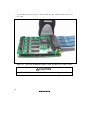
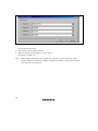
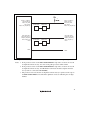
1
REJ10J1237-0400
SH-2A, SH-2 E200F Emulator
Additional Document for User’s Manual
Supplementary Information on Using the SH7083, SH7084,
SH7085, SH7086, SH7146, SH7149, SH7124, and SH7125
Renesas Microcomputer Development Environment System
SuperH™ Family / SH7080 Series
/ SH7146 Series
/ SH7125 Series
E200F for SH7080 R0E570800EMU00E
Rev.4.00
Revision Date: Feb. 26, 2007
Notes regarding these materials
1. This document is provided for reference purposes only so that Renesas customers may select the appropriate
Renesas products for their use. Renesas neither makes warranties or representations with respect to the
accuracy or completeness of the information contained in this document nor grants any license to any
intellectual property rights or any other rights of Renesas or any third party with respect to the information in
this document.
2. Renesas shall have no liability for damages or infringement of any intellectual property or other rights arising
out of the use of any information in this document, including, but not limited to, product data, diagrams, charts,
programs, algorithms, and application circuit examples.
3. You should not use the products or the technology described in this document for the purpose of military
applications such as the development of weapons of mass destruction or for the purpose of any other military
use. When exporting the products or technology described herein, you should follow the applicable export
control laws and regulations, and procedures required by such laws and regulations.
4. All information included in this document such as product data, diagrams, charts, programs, algorithms, and
application circuit examples, is current as of the date this document is issued. Such information, however, is
subject to change without any prior notice. Before purchasing or using any Renesas products listed in this
document, please confirm the latest product information with a Renesas sales office. Also, please pay regular
and careful attention to additional and different information to be disclosed by Renesas such as that disclosed
through our website. (http://www.renesas.com )
5. Renesas has used reasonable care in compiling the information included in this document, but Renesas
assumes no liability whatsoever for any damages incurred as a result of errors or omissions in the information
included in this document.
6. When using or otherwise relying on the information in this document, you should evaluate the information in
light of the total system before deciding about the applicability of such information to the intended application.
Renesas makes no representations, warranties or guaranties regarding the suitability of its products for any
particular application and specifically disclaims any liability arising out of the application and use of the
information in this document or Renesas products.
7. With the exception of products specified by Renesas as suitable for automobile applications, Renesas
products are not designed, manufactured or tested for applications or otherwise in systems the failure or
malfunction of which may cause a direct threat to human life or create a risk of human injury or which require
especially high quality and reliability such as safety systems, or equipment or systems for transportation and
traffic, healthcare, combustion control, aerospace and aeronautics, nuclear power, or undersea communication
transmission. If you are considering the use of our products for such purposes, please contact a Renesas
sales office beforehand. Renesas shall have no liability for damages arising out of the uses set forth above.
8. Notwithstanding the preceding paragraph, you should not use Renesas products for the purposes listed below:
(1) artificial life support devices or systems
(2) surgical implantations
(3) healthcare intervention (e.g., excision, administration of medication, etc.)
(4) any other purposes that pose a direct threat to human life
Renesas shall have no liability for damages arising out of the uses set forth in the above and purchasers who
elect to use Renesas products in any of the foregoing applications shall indemnify and hold harmless Renesas
Technology Corp., its affiliated companies and their officers, directors, and employees against any and all
damages arising out of such applications.
9. You should use the products described herein within the range specified by Renesas, especially with respect
to the maximum rating, operating supply voltage range, movement power voltage range, heat radiation
characteristics, installation and other product characteristics. Renesas shall have no liability for malfunctions or
damages arising out of the use of Renesas products beyond such specified ranges.
10. Although Renesas endeavors to improve the quality and reliability of its products, IC products have specific
characteristics such as the occurrence of failure at a certain rate and malfunctions under certain use
conditions. Please be sure to implement safety measures to guard against the possibility of physical injury, and
injury or damage caused by fire in the event of the failure of a Renesas product, such as safety design for
hardware and software including but not limited to redundancy, fire control and malfunction prevention,
appropriate treatment for aging degradation or any other applicable measures. Among others, since the
evaluation of microcomputer software alone is very difficult, please evaluate the safety of the final products or
system manufactured by you.
11. In case Renesas products listed in this document are detached from the products to which the Renesas
products are attached or affixed, the risk of accident such as swallowing by infants and small children is very
high. You should implement safety measures so that Renesas products may not be easily detached from your
products. Renesas shall have no liability for damages arising out of such detachment.
12. This document may not be reproduced or duplicated, in any form, in whole or in part, without prior written
approval from Renesas.
13. Please contact a Renesas sales office if you have any questions regarding the information contained in this
document, Renesas semiconductor products, or if you have any other inquiries.
Contents
Section 1 System Configuration ............................................................................1
1.1
1.2
Components of the Emulator ................................................................................................. 1
System Configuration ............................................................................................................ 8
Section 2 Connecting the Emulator to the User System ......................................11
2.1
2.2
2.3
2.4
2.5
2.6
Connecting the Emulator to the User System ...................................................................... 11
Connecting the Emulator to the User System by Using the EV-chip Unit........................... 11
2.2.1 Connecting the EV-chip Unit to the Emulator ........................................................ 11
2.2.2 Connecting the E200F External Bus Trace Unit to the EV-chip Unit .................... 14
2.2.3 Connecting the Probe Head to the EV-chip Unit .................................................... 16
2.2.4 Connecting the E200F Emulation Memory Unit to the EV-chip Unit.................... 17
2.2.5 Connecting the E200F External Bus Trace Unit, Emulation Memory Unit,
and EV-chip Unit .................................................................................................... 19
2.2.6 Connecting the EV-chip Unit to the User System Interface Board......................... 20
Connecting the Emulator to the User System by Using the H-UDI Port Connector............ 21
Installing the H-UDI Port Connector on the User System ................................................... 22
Pin Assignments of the H-UDI Port Connector ................................................................... 22
Recommended Circuit between the H-UDI Port Connector and the MCU ......................... 24
2.6.1 Recommended Circuit (36-Pin Type) ..................................................................... 24
Section 3 Software Specifications when Using the SH7080 Series/
SH7146 Series/SH7125 Series.............................................................27
3.1
3.2
Differences between the MCU and the Emulator ................................................................ 27
Specific Functions for the Emulator when Using the SH7080 Series/SH7146 Series/
SH7125 Series...................................................................................................................... 35
3.2.1 Event Condition Functions ..................................................................................... 35
3.2.2 Trace Functions....................................................................................................... 42
3.2.3 Notes on Using the JTAG (H-UDI) Clock (TCK) and AUD Clock (AUDCK)...... 55
3.2.4 Notes on Setting the [Breakpoint] Dialog Box ....................................................... 56
3.2.5 Notes on Setting the [Event Condition] Dialog Box and
the BREAKCONDITION_ SET Command ........................................................... 56
3.2.6 Performance Measurement Function ...................................................................... 57
Section 4 User System Interface Circuits ............................................................61
4.1
4.2
User System Interface Circuits............................................................................................. 61
User System Interface Board Circuits.................................................................................. 73
i
4.3
ii
Delay Time for the User System Interface........................................................................... 79
Section 1 System Configuration
1.1
Components of the Emulator
The E200F emulator supports the SH7080 series, SH7146 series, and SH7125 series:
SH7083 (R5E SH7083 (R5E70835R/R5F70834A/R5F70835A), SH7084
(R5E70845R/R5F70844A/R5F70845A), SH7085 (R5E70855R/ R5F70854A/R5F70855A),
SH7086 (R5E70865R/R5F70865A), SH7146 (R5E71464R/R5F71464R), SH7149
(R5E71494R/R5F71494R/R5E71491R/R5F71491R), SH7124, and SH7125. Table 1.1 lists the
components of the emulator.
1
Table 1.1 Components of the Emulator
Classification Component
Hardware
Emulator main unit
AC adapter
Appearance
Quantity
1
Remarks
R0E0200F1EMU00:
Depth: 195.0 mm, Width: 130.0
mm,
Height: 45.0 mm, Mass: 490.0 g
Product numbers: 0001 to 0113
1
Input: 100 to 240 V
Output: 12 V 4.0 A
Depth: 120.0 mm, Width: 72.0 mm,
Height: 27.0 mm, Mass: 400.0 g
Product numbers: 0114 or later
1
Input: 100 to 240 V
Output: 12 V 3.0 A
Depth: 99.0 mm, Width: 62.0 mm,
Height: 26.0 mm, Mass: 270.0 g
AC cable
2
1
Length: 2000 mm
Table 1.1 Components of the Emulator (cont)
Classification Component
Hardware
(cont)
USB cable
External probe
Appearance
Quantity
Remarks
1
Length: 1500 mm, Mass: 50.6 g
Product numbers: 0001 to 0113
1
Length: 500 mm,
Pins 1 to 4: probe input pins,
T: trigger output pin,
G: GND pin
Product numbers: 0114 or after
1
Length: 500 mm,
Pins 1 to 4: probe input pins,
T: trigger output pin,
G: GND pin
Software
E200F emulator setup
1
R0E0200F1EMU00S,
program,
SH-2A, SH-2 E200F
R0E0200F1EMU00J,
Emulator User’s Manual,
R0E0200F1EMU00E,
and
Supplementary
R0E570800EMU00J, and
Information on Using the
R0E570800EMU00E
SH7083, SH7084,
(provided on a CD-R)
SH7085, SH7086,
SH7146, SH7149,
SH7124, and SH7125*
Note: Additional document for the MCUs supported by the emulator is included. Check the target
MCU and refer to its additional document.
3
Table 1.2 Optional Components of the Emulator
Classification Component
Hardware
4
Appearance
Quantity
Remarks
Expansion profiling unit
1
R0E0200F0EPU00:
Depth: 98.0 mm, Width: 115.0 mm,
Height: 15.2 mm, Mass: 52 g
External bus trace unit
1
R0E0200F1ETU00:
Depth: 90.0 mm, Width: 125.0 mm,
Height: 15.2 mm, Mass: 83 g
Emulation memory unit
(Memory capacity:
8 Mbytes or 16 Mbytes)
1
EV-chip unit
1
R0E0200F1MSR00 (8 Mbytes),
R0E0200F1MSR01 (16 Mbytes):
Depth: 90.0 mm, Width: 125.0 mm,
Height: 15.2 mm,
Mass: 81 g (R0E0200F1MSR00),
85 g (R0E0200F1MSR01)
Note that it is not possible to
connect these emulation memory
units at the same time.
R0E570800VKK00:
Depth: 110.0 mm, Width: 125.0
mm, Height: 15.2 mm, Mass: 110 g
Trace cable
1
R0E0200F0ACC00:
Length: 300 mm, Mass: 65 g
Table 1.2 Optional Components of the Emulator (cont)
Classification Component
Hardware
(cont)
Appearance
Quantity
Remarks
SH7083 (PTQP0100KAA) user system interface
board
1
R0E570830CFK00:
Depth: 60.0 mm, Width: 90.0 mm,
Height: 26.0 mm, Mass: 45 g
SH7084 (PLQP0112JA-A)
user system interface
board
1
R0E570840CFJ00:
Depth: 60.0 mm, Width: 90.0 mm,
Height: 26.0 mm, Mass: 45 g
SH7085 (PLQP0144KAA) user system interface
board
1
R0E570850CFK00:
Depth: 60.0 mm, Width: 90.0 mm,
Height: 26.0 mm, Mass: 45 g
SH7086 (PLQP0176KBA) user system interface
board
1
R0E570860CFK00:
Depth: 60.0 mm, Width: 90.0 mm,
Height: 26.0 mm, Mass: 45 g
5
Table 1.2 Optional Components of the Emulator (cont)
Classification Component
Hardware
(cont)
6
Appearance
Quantity
Remarks
SH7146 (PLQP0080JA-A)
user system interface
board
1
R0E571460CFJ00:
Depth: 60.0 mm, Width: 90.0 mm,
Height: 26.0 mm, Mass: 45 g
SH7149 (PLQP0100KBA) user system interface
board
1
R0E571490CFK00:
Depth: 60.0 mm, Width: 90.0 mm,
Height: 26.0 mm, Mass: 45 g
SH7149 (PRQP0100JEB) user system interface
board
1
R0E571490CFJ00:
Depth: 60.0 mm, Width: 90.0 mm,
Height: 26.0 mm, Mass: 45 g
SH7125 (PLQP0064KBA) user system interface
board
1
R0E571250CFK00:
Depth: 60.0 mm, Width: 90.0 mm,
Height: 26.0 mm, Mass: 45 g
Table 1.2 Optional Components of the Emulator (cont)
Classification Component
Hardware
(cont)
Appearance
Quantity
Remarks
SH7125 (PRQP0064GBA) user system interface
board
1
R0E571250CFG00:
Depth: 60.0 mm, Width: 90.0 mm,
Height: 26.0 mm, Mass: 45 g
SH7124 (PLQP0048JA-A)
user system interface
board
1
R0E571240CFJ00:
Depth: 60.0 mm, Width: 90.0 mm,
Height: 26.0 mm, Mass: 45 g
7
1.2
System Configuration
Figure 1.1 shows an example of the emulator system configuration.
- When the EV-chip unit is not used:
Expansion profiling unit
High-performance
Embedded Workshop
H-UDI port
connector
E200F
User system
PC
- When the EV-chip unit is used:
Expansion profiling unit
Trace cable
High-performance
Embedded Workshop
External bus
trace unit
Emulation memory unit
User system
interface board
EV-chip unit
IC socket
PC
E200F
User system
Figure 1.1 System Configuration Using the Emulator
(1) System Configuration of the SH7080 Series and SH7149
Table 1.3 shows the system configuration supported by the SH7080 series
(SH7083/SH7084/SH7085/SH7086) and SH7149.
8
Table 1.3 System Configuration Supported by the SH7080 Series and SH7149 E200F
Emulation Memory
Unit
Trace Unit
R0E0200F1MSR00 Unit
Trace Cable
R0E0200F1EMU00 R0E570800VKK00 R0E0200F1ETU00
R0E0200F1MSR01 R0E0200F0EPU00
R0E0200F0ACC00 Board
Supported
Not supported
Not supported
Not supported
Not supported
Not supported
Not supported
Supported
Supported
Not supported
Not supported
Not supported
Supported
Supported
Supported
Supported
Supported
Not supported
Not supported
Supported
Supported
Supported
Supported
Not supported
Supported
Not supported
Supported
Supported*3
Supported
Supported
Supported
Supported
Not supported
Supported
Supported*3
Supported
Not supported
Not supported
Not supported
Supported
Not supported
Not supported
Supported
Supported
Not supported
Not supported
Supported
Supported
Supported*3
Supported
Supported
Supported
Not supported
Supported
Supported
Supported*3
Supported
Supported
Not supported
Supported
Supported
Supported
Supported*3
Supported
Supported
Supported
Supported
Supported
Supported
Supported*3
E200F Emulator
System
User
External Bus
EV-chip Unit
Expansion Profiling
System
Interface
configuration
1*1, *2
System
*3
configuration
2
System
*3
configuration
3
System
configuration
4
System
configuration
5
System
configuration
6
*1, *2
System
configuration
7
System
configuration
8
System
configuration
9
System
configuration
10
Notes: 1. When system configuration 1 or 6 is used, the H-UDI port connector must be installed
on the user system. When designing the user system, refer to section 2.3, Connecting
the Emulator to the User System by Using the H-UDI Port Connector. For system
configuration 1 or 6, note that the H-UDI pin of the MCU is occupied by the emulator.
2. When system configuration 1 or 6 is used, note that the AUD pin of the MCU is
occupied by the emulator.
3. The user system interface board is only used when the emulator is connected to the
user system; it is not required when the emulator system operates alone.
9
(2) System Configuration of the SH7125 Series and SH7146
Table 1.4 shows the system configuration supported by the SH7125 series (SH7124/SH7125)
and SH7146.
Table 1.4 System Configuration Supported by the SH7125 Series and SH7146 E200F
Emulation Memory
Unit
Trace Unit
R0E0200F1MSR00 Profiling Unit
Trace Cable
R0E0200F1EMU00 R0E570800VKK00 R0E0200F1ETU00
R0E0200F1MSR01 R0E0200F0EPU00
R0E0200F0ACC00 Board
Supported
Not supported
Not supported
Not supported
Not supported
Not supported
Not supported
Supported
Supported
Not supported
Not supported
Not supported
Supported
Supported*2
Supported
Supported
Not supported
Not supported
Supported
Supported
Supported*2
E200F Emulator
System
User
External Bus
EV-chip Unit
Expansion
System
Interface
configuration
1*1
System
configuration
2
System
configuration
3
Notes: 1. When system configuration 1 is used, the H-UDI port connector must be installed on
the user system. When designing the user system, refer to section 2.3, Connecting the
Emulator to the User System by Using the H-UDI Port Connector. For system
configuration 1, note that the H-UDI pin of the MCU is occupied by the emulator.
2. The user system interface board is only used when the emulator is connected to the
user system; it is not required when the emulator system operates alone.
10
Section 2 Connecting the Emulator to the User System
2.1
Connecting the Emulator to the User System
When the emulator is connected to the user system, use the optional EV-chip unit, user system
interface board, and trace cable, or install the H-UDI port connector on the user system.
2.2
Connecting the Emulator to the User System by Using the EV-chip
Unit
The following describes how to connect the emulator to the EV-chip unit, external bus trace unit,
emulation memory unit, trace cable, and user system interface board.
2.2.1
Connecting the EV-chip Unit to the Emulator
•
Open the cover of TRACE I/F on the side of the main unit case.
•
Connect the trace cable to the EV-chip unit as shown in figure 2.1.
11
Figure 2.1 Connecting the Trace Cable to E200F when Using the EV-chip Unit
12
•
Connect the EV-chip unit to the trace cable (CN1 side).
Figure 2.2 Connecting the Trace Cable to the EV-chip Unit
CAUTION
Check the location of pin 1 before connecting.
13
2.2.2
•
Connecting the E200F External Bus Trace Unit to the EV-chip Unit
When the external bus trace unit is used with the EV-chip unit, connect the external bus trace
unit to the EV-chip unit as shown in figure 2.3.
Figure 2.3 Connecting the External Bus Trace Unit to the EV-chip Unit
14
•
After checking the location of pin 1, connect the EV-chip unit, external bus trace unit, and
trace cable.
Figure 2.4 Connecting the EV-chip Unit, External Bus Trace Unit, and Trace Cable
CAUTION
Check the location of pin 1 before connecting.
15
2.2.3
•
Connecting the Probe Head to the EV-chip Unit
Connect the probe head to the EV-chip unit as shown in figure 2.5.
Figure 2.5 Connecting the Probe Head to the EV-chip Unit
CAUTION
Check the location of pin 1 before connecting.
16
2.2.4
•
Connecting the E200F Emulation Memory Unit to the EV-chip Unit
When the emulation memory unit is used with the EV-chip unit, connect the emulation
memory unit to the EV-chip unit (figure 2.6).
Figure 2.6 Connecting the Emulation Memory Unit to the EV-chip Unit
17
•
After checking the location of pin 1, connect the EV-chip unit, emulation memory unit, and
trace cable.
Figure 2.7 Connecting the Emulation Memory Unit, EV-chip Unit, and Trace Cable
CAUTION
Check the location of pin 1 before connecting.
18
2.2.5
Connecting the E200F External Bus Trace Unit, Emulation Memory Unit, and EVchip Unit
•
When the external bus trace unit is used with the emulation memory unit and EV-chip unit, as
shown in figure 2.8, connect them in the positions of (a), (b), and (c) for the external bus trace
unit, emulation memory unit, and EV-chip unit, respectively.
•
After checking the location of pin 1, connect the external bus trace unit, emulation memory
unit, and EV-chip unit.
Figure 2.8 Connecting the External Bus Trace Unit, Emulation Memory Unit, and EV-chip
Unit
CAUTION
Check the location of pin 1 and the position of each unit
before connecting.
19
2.2.6
•
Connecting the EV-chip Unit to the User System Interface Board
After checking the location of pin 1, connect the EV-chip unit to the user system interface
board.
EV-chip unit
Connector No.
EV-Chip Unit
Connector No.
User I/F Connector 1
(CN4)
User I/F Connector 2
(CN5)
Board
Connector No.
UCN1
UCN2
Board
Spacer
User system
Figure 2.9 Connecting User System Interface Board to EV-Chip Unit
CAUTION
Check the location of pin 1 before connecting.
Notes: 1. Connection of the signals differs depending on the MCU used.
2. For the method to connect the user system interface board to the user system, refer to
the user system interface board user’s manual for each MCU.
20
2.3
Connecting the Emulator to the User System by Using the H-UDI
Port Connector
When the H-UDI port connector is installed on the user system, refer to the recommended circuit
between the H-UDI port connector and the MCU.
It is impossible to connect the emulator to the 14-pin type connector that is recommended for the
E10A-USB emulator. The 36-pin type connector is the same as that of the E10A-USB emulator.
When designing the user system, read the E200F emulator user's manual and hardware manual for
the related device.
Table 2.1 shows the type number of the emulator, the corresponding connector type, and the use of
AUD function.
Table 2.1 Type Number, AUD Function, and Connector Type
Type Number
Connector
AUD Function
R0E0200F1EMU00
14-pin connector
Not available
R0E0200F1EMU00
36-pin connector
Available
The H-UDI port connector has the 36-pin and 14-pin types as described below. Use the 36-pin
connector when using the emulator.
1. 36-pin type (with AUD function)
The AUD trace function is supported. A large amount of trace information can be acquired in
realtime. The window trace function is also supported for acquiring memory access in the
specified range (memory access address or memory access data) by tracing.
2. 14-pin type (without AUD function)
The AUD trace function cannot be used because only the H-UDI function is supported. This
connector type is not available for the emulator. Use the E10A-USB emulator.
Notes: 1. In the R5E70855R or R5E70865R, the AUD pins (AUDCK, AUDATA3 to
AUDATA0, and _AUDSYNC) are assigned to two different pins. When the AUD
function is used, connect either of pins to the H-UDI port connector.
2. The 36-pin H-UDI port connector is required to connect the emulator. When the MCU
does not support the AUD function or the AUD function is not used, do not connect
anything to the AUD pins (AUDCK, AUDATA3 to AUDATA0, and _AUDSYNC) of
the H-UDI port connector.
21
2.4
Installing the H-UDI Port Connector on the User System
Table 2.2 shows the recommended H-UDI port connectors for the emulator.
Table 2.2 Recommended H-UDI Port Connectors
Connector
Type Number
Manufacturer
Specifications
36-pin connector
DX10M-36S
Hirose Electric Co., Ltd.
Screw type
DX10M-36SE,
DX10G1M-36SE
Lock-pin type
Note: When designing the 36-pin connector layout on the user board, do not connect any
components under the H-UDI connector.
2.5
Pin Assignments of the H-UDI Port Connector
Figure 2.10 shows the pin assignments of the 36-pin H-UDI port connectors.
Note: Note that the pin number assignments of the H-UDI port connector shown on the
following page differ from those of the connector manufacturer.
22
Pin
No. Signal
Input/
Output*1
1
AUDCK*5
2
GND
3
AUDATA0*5
Pin
No.
Note
Output
4
GND
5
AUDATA1*5
6
GND
7
AUDATA2 *5
8
GND
9
AUDATA3*5
10
GND
_AUDSYNC
19
Output
Output
Output
Input/
Output*1
TMS
Input
20
GND
21
_TRST
22
(GND)*4
23
TDI
24
GND
25
TDO
26
GND
27
Output
Signal
*2
GND
29
UVCC
12
GND
30
GND
13
N.C.
31
_RES*2
14
GND
32
GND
15
11
Output
*2, *5
N.C.
33
GND *3
16
GND
34
GND
17
TCK
35
N.C.
18
GND
36
GND
Input
Input
Input
Output
_ASEBRKAK
/_ASEBRK *2
28
Note
Input/
output
Output
Output
User reset
Output
Notes: 1. Input to or output from the user system.
2. The symbol (_) means that the signal is active-low.
3. The emulator monitors the GND signal of the user system and detects whether or not the user system is connected.
4. When the E200F probe head is connected to this pin and the _ASEMD pin is set to 0, do not connect to GND
but to the _ASEMD pin directly.
5. When the MCU does not support the AUD function or the AUD function is not used, do not connect anything to the
AUD pins (AUDCK, AUDATA3 to AUDATA0, and _AUDSYNC) of the H-UDI port connector.
H-UDI port connector (top view)
Edge of the board
(connected to the connector)
φ 0.7+0.1
0
36
1
3
9.0
1.905
1.1
4.5
2
φ 2.8+0.1
0
4
(Pin 1 mark)
35
1.27
4.09
M2.6 x 0.45
H-UDI port connector (front view)
4.8
H-UDI port connector (top view)
3.9
37.61
43.51
: Pattern inhibited area
0.3
9.0
21.59
Unit: mm
Figure 2.10 Pin Assignments of the H-UDI Port Connector (36 Pins)
23
2.6
Recommended Circuit between the H-UDI Port Connector and the
MCU
2.6.1
Recommended Circuit (36-Pin Type)
Figure 2.11 shows a recommended circuit for connection between the H-UDI and AUD port
connectors (36 pins) and the MCU when the emulator is in use.
Notes: 1. Do not connect anything to the N.C. pins of the H-UDI port connector.
2.
The _ASEMD pin must be 0 when the emulator is connected and 1 when the emulator
is not connected, respectively.
(1) When the emulator is used: _ASEMD = 0 (ASE mode)
(2) When the emulator is not used: _ASEMD = 1 (normal mode)
Figure 2.11 shows an example of circuits that allow the _ASEMD pin to be GND (0)
whenever the emulator is connected by using the user system interface cable.
3.
When a network resistance is used for pull-up, it may be affected by a noise. Separate
TCK from other resistances.
4.
The pattern between the H-UDI port connector and the MCU must be as short as
possible. Do not connect the signal lines to other components on the board.
5.
The AUD signals (AUDCK, AUDATA3 to AUDATA0, and _AUDSYNC) operate in
high speed. Isometric connection is needed if possible. Do not separate connection nor
connect other signal lines adjacently.
6.
Supply the operating voltages of the H-UDI and AUD of the MCU to the UVCC pin.
7.
The resistance values shown in figure 2.11 are for reference.
8.
For the pin processing in cases where the emulator is not used, refer to the hardware
manual of the related MCU.
9.
For the AUDCK pin, guard the pattern between the H-UDI port connector and the
MCU at GND level.
10. When the MCU does not support the AUD function or the AUD function is not used,
do not connect anything to the AUD pins (AUDCK, AUDATA3 to AUDATA0, and
_AUDSYNC) of the H-UDI port connector.
24
Vcc = I/O power supply
Vcc
Vcc
Vcc
All pulled-up at 4.7 kΩ or more
H-UDI port connector
(36-pin type)
2
4
6
8
10
12
14
16
18
20
22
24
GND
AUDCK
GND
AUDATA0
GND
AUDATA1
GND
AUDATA2
GND
AUDATA3
GND
AUDSYNC
GND
N.C.
GND
N.C.
GND
TCK
GND
TMS
(GND)
GND
TRST
TDI
Target MCU
1
AUDCK
3
AUDATA0
5
AUDATA1
7
AUDATA2
9
AUDATA3
11
AUDSYNC
13
15
17
TCK
19
TMS
21
TRST
23
TDI
25
TDO
ASEBRKAK 27
GND
/ASEBRK
29
30
UVCC*
GND
31
32
GND
RES
33
34
GND
GND
36
35
N.C.
GND
26
Vcc
GND
TDO
28
ASEBRKAK
/ASEBRK
RES
ASEMD0
Reset signal
User system
Note: Supply the operating voltages of the H-UDI and AUD of the MCU to the UVCC pin.
Figure 2.11 Recommended Circuit for Connection between the H-UDI Port Connector and
MCU when the Emulator is in Use (36-Pin Type)
25
26
Section 3 Software Specifications when Using the SH7080
Series/SH7146 Series/SH7125 Series
3.1
Differences between the MCU and the Emulator
1. When the emulator system is initiated, it initializes the general registers and part of the control
registers as shown in table 3.1. The initial values of the MCU are undefined. When the
emulator is initiated from the workspace, a value to be entered is saved in a session.
Table 3.1 Register Initial Values at Emulator Link Up
Register
Emulator at Link Up
R0 to R14
H'00000000
R15 (SP)
Value of the SP in the power-on reset vector table
PC
Value of the PC in the power-on reset vector table
SR
H'000000F0
GBR
H'00000000
VBR
H'00000000
MACH
H'00000000
MACL
H'00000000
PR
H'00000000
2. The emulator uses the H-UDI; do not access the H-UDI.
3. Low-Power States (Sleep, Software Standby, and Module Standby)
• When the emulator is used, the sleep state can be cleared with either the clearing function
or with the [STOP] button, and a break will occur.
• The memory must not be accessed or modified in software standby state.
• When the emulator is used, do not use the deep software standby mode.
4. Reset Signals
The MCU reset signals are only valid during emulation started with clicking the GO or STEPtype button. If these signals are enabled on the user system in command input wait state, they
are not sent to the MCU.
Note: Do not break the user program when the _RES, _BREQ, or _WAIT signal is being low. A
TIMEOUT error will occur. If the _BREQ or _WAIT signal is fixed to low during break,
a TIMEOUT error will occur at memory access. (Some MCUs will incorporate no _BREQ
or _WAIT.)
27
5. Direct Memory Access Controller (DMAC)/Data Transfer Controller (DTC)
When the MCU incorporates a DMAC, the DMAC operates even when the emulator is used.
When a data transfer request is generated, the DMAC executes DMA transfer.
When the MCU incorporates a DTC, the DTC operates even when the emulator is used. When
a data transfer request is generated, the DTC executes DTC transfer.
6. Memory Access during User Program Execution
During execution of the user program, memory is accessed by the following two methods, as
shown in table 3.2.
Table 3.2 Memory Access during User Program Execution
Method
Description
H-UDI read/write
The stopping time of the user program is short because memory is
accessed by the dedicated bus master.
Short break
This method is not used in this product. (Do not set short break.)
The method for accessing memory during execution of the user program is specified by using
the [Configuration] dialog box.
Table 3.3 Stopping Time by Memory Access (Reference)
Method
Condition
Stopping Time
H-UDI read/write
Reading of one longword for the
internal RAM
Reading: Maximum two bus clock
cycles (Bφ)
Writing of one longword for the
internal RAM
Writing: Maximum two bus clock
cycles (Bφ)
7. Memory Access to the External Flash Memory Area
The emulator can download the load module to the external flash memory area (for details,
refer to section 6.21, Download Function to the Flash Memory Area, in the SH-2A, SH-2
E200F Emulator User’s Manual). Neither memory write nor BREAKPOINT setting is enabled
for the external flash memory area. To set the break condition for the program on the external
flash memory, use the Event Condition function.
Some MCUs will incorporate no external flash memory area.
8. Using WDT
The WDT does not operate during break.
28
9. Loading Sessions
Information in [JTAG clock] of the [Configuration] dialog box cannot be recovered by loading
sessions. Thus the TCK value will be 2.5 MHz.
10. [IO] Window
• Display and modification
For each watchdog timer register, there are two registers to be separately used for write and
read operations.
Table 3.4 Watchdog Timer Register
Register Name
Usage
Register
WTCSR (W)
Write
Watchdog timer control/status register
WTCNT (W)
Write
Watchdog timer counter
WTCSR(R)
Read
Watchdog timer control/status register
WTCNT(R)
Read
Watchdog timer counter
After the I/O-register definition file is created, the MCU’s specifications may be changed.
If each I/O register in the I/O-register definition file differs from addresses described in the
hardware manual, change the I/O-register definition file according to the description in the
hardware manual. The I/O-register definition file can be customized depending on its
format. Note that, however, the emulator does not support the bit-field function.
• Verify
In the [IO] window, the verify function of the input value is disabled.
11. Illegal Instructions
Do not execute illegal instructions with STEP-type commands.
12. MCU Operating Mode
Do not use the emulator in the boot, user boot, and user program modes.
13. Internal Flash Memory
It is not possible to reprogram the content of the internal flash memory during execution of the
user program.
29
14. Multiplexing the AUD Pins in Debugging without Connecting the EV-chip Unit
When debugging is performed without connecting the EV-chip unit, the AUD pin is
multiplexed as shown in table 3.5.
Table 3.5 Multiplexed Functions
MCU
Function 1
Function 2
R5E70835R
PE0/DREQ0/TIOC0A
TMS
PE1/TEND0/TIOC0B
_TRST
PE2/DREQ1/TIOC0C
TDI
PE3/TEND1/TIOC0D
TDO
R5E70845R
30
PE4/TIOC1A/RXD3
TCK
PE13/TIOC4B/_MRES
_ASEBRKAK/_ASEBRK
PD8/D8/TIOC3AS
AUDATA0
PD9/D9/TIOC3BS
AUDATA1
PD10/D10/TIOC3CS
AUDATA2
PD11/D11/TIOC3DS
AUDATA3
PD14/D14/TIOC4CS
AUDCK
PD15/D15/TIOC4DS
_AUDSYNC
PE0/DREQ0/TIOC0A
TMS
PE1/TEND0/TIOC0B
_TRST
PE2/DREQ1/TIOC0C
TDI
PE3/TEND1/TIOC0D
TDO
PE4/TIOC1A/RXD3
TCK
PE5/_CS6/TIOC1B/TXD3
_ASEBRKAK/_ASEBRK
PD8/D8/TIOC3AS
AUDATA0
PD9/D9/TIOC3BS
AUDATA1
PD10/D10/TIOC3CS
AUDATA2
PD11/D11/TIOC3DS
AUDATA3
PD14/D14/TIOC4CS
AUDCK
PD15/D15/TIOC4DS
_AUDSYNC
Table 3.5 Multiplexed Functions (cont)
MCU
Function 1
Function 2
R5E70855R
PE8/TIOC3A/SCK2/SSCK
TMS
PE9/TIOC3B/SCK3/_RTS3
_TRST
PE10/TIOC3C/TXD2/SSO
TDI
PE11/TIOC3D/RXD3/_CTS3
TDO
PE12/TIOC4A/TXD3/_SCS
TCK
PE13/TIOC4B/_MRES
_ASEBRKAK/_ASEBRK
PD16/D16/IRQ0/_POE4
AUDATA0
PD17/D17/IRQ1/_POE5
AUDATA1
PD18/D18/IRQ2/_POE6
AUDATA2
PD19/D19/IRQ3/_POE7
AUDATA3
R5E70865R
PD22/D22/IRQ6/TIC5US
AUDCK
PD23/D23/IRQ7
_AUDSYNC
PA16/_WRHH/_ICIOWR/_AH/
DQMUU/CKE/DREQ2
_AUDSYNC
PE0/DREQ0/TIOC0A
AUDCK
PE3/TEND1/TIOC0D
AUDATA3
PE4/_IOIS16/TIOC1A/RXD3
AUDATA2
PE5/_CS6/_CE1B/TIOC1B/TXD3
AUDATA1
PE6/_CS7/TIOC2A/SCK3
AUDATA0
PE8/TIOC3A/SCK2/SSCK
TMS
PE9/TIOC3B/SCK3/_RTS3
_TRST
PE10/TIOC3C/TXD2/SSO
TDI
PE11/TIOC3D/RXD3/_CTS3
TDO
PE12/TIOC4A/TXD3/_SCS
TCK
PE13/TIOC4B/_MRES
_ASEBRKAK/_ASEBRK
PD16/D16/IRQ0/_POE4
AUDATA0
PD17/D17/IRQ1/_POE5
AUDATA1
PD18/D18/IRQ2/_POE6
AUDATA2
PD19/D19/IRQ3/_POE7
AUDATA3
PD22/D22/IRQ6/TIC5US
AUDCK
PD23/D23/IRQ7
_AUDSYNC
31
Table 3.5 Multiplexed Functions (cont)
MCU
Function 1
Function 2
R5E70865R (cont)
PA16/_WRHH/_ICIOWR/_AH/
DQMUU/CKE/DREQ2
_AUDSYNC
PE0/DREQ0/TIOC0A
AUDCK
PE3/TEND1/TIOC0D
AUDATA3
PE4/_IOIS16/TIOC1A/RXD3
AUDATA2
PE5/_CS6/_CE1B/TIOC1B/TXD3
AUDATA1
PE6/_CS7/TIOC2A/SCK3
AUDATA0
R5F70834A and
PE0/DREQ0/TIOC0A
TMS
R5F70835A
PE1/TEND0/TIOC0B
_TRST
PE2/DREQ1/TIOC0C
TDI
PE3/TEND1/TIOC0D
TDO
PE4/TIOC1A/RXD3
TCK
PE13/TIOC4B/_MRES
_ASEBRKAK/_ASEBRK
R5F70844A and
PE0/DREQ0/TIOC0A
TMS
R5F70845A
PE1/TEND0/TIOC0B
_TRST
PE2/DREQ1/TIOC0C
TDI
PE3/TEND1/TIOC0D
TDO
PE4/TIOC1A/RXD3
TCK
PE5/_CS6/TIOC1B/TXD3
_ASEBRKAK/_ASEBRK
R5F70854A and
PE8/TIOC3A/SCK2/SSCK
TMS
R5F70855A
PE9/TIOC3B/SCK3/_RTS3
_TRST
PE10/TIOC3C/TXD2/SSO
TDI
PE11/TIOC3D/RXD3/_CTS3
TDO
PE12/TIOC4A/TXD3/_SCS
TCK
PE13/TIOC4B/_MRES
_ASEBRKAK/_ASEBRK
PE8/TIOC3A/SCK2/SSCK
TMS
R5F70865A
32
PE9/TIOC3B/SCK3/_RTS3
_TRST
PE10/TIOC3C/TXD2/SSO
TDI
PE11/TIOC3D/RXD3/_CTS3
TDO
PE12/TIOC4A/TXD3/_SCS
TCK
PE13/TIOC4B/_MRES
_ASEBRKAK/_ASEBRK
Table 3.5 Multiplexed Functions (cont)
MCU
Function 1
Function 2
R5E71464R
PE16/TIOC3BS
_ASEBRKAK/_ASEBRK
PE17/TIOC3DS
TCK
PE18/TIOC4AS
TDI
PE19/TIOC4BS
TDO
PE20/TIOC4CS
TMS
PE21/TIOC4DS
_TRST
R5E71494R and
PE16/_WAIT/TIOC3BS
_ASEBRKAK/_ASEBRK
R5E71491R
PE17/_CS0/TIOC3DS
TCK
PE18/_CS1/TIOC4AS
TDI
PE19/_RD/TIOC4BS
TDO
PE20/_WRH/TIOC4CS
TMS
PE21/_WRL/TIOC4DS
_TRST
PD8/D8/SCK2
AUDATA0
PD9/D9
AUDATA1
PD10/D10
AUDATA2
PD11/D11
AUDATA3
PD14/D14
AUDCK
PD15/D15
_AUDSYNC
PE16/TIOC3BS
_ASEBRKAK/_ASEBRK
PE17/TIOC3DS
TCK
PE18/TIOC4AS
TDI
PE19/TIOC4BS
TDO
PE20/TIOC4CS
TMS
PE21/TIOC4DS
_TRST
R5F71494R
PE16/_WAIT/TIOC3BS
_ASEBRKAK/_ASEBRK
R5F71491R
PE17/_CS0/TIOC3DS
TCK
R5F71464R
PE18/_CS1/TIOC4AS
TDI
PE19/_RD/TIOC4BS
TDO
PE20/_WRH/TIOC4CS
TMS
PE21/_WRL/TIOC4DS
_TRST
33
Table 3.5 Multiplexed Functions (cont)
MCU
Function 1
Function 2
SH7125
FWE
_ASEBRKAK/_ASEBRK
PA3/_IRQ1/RXD1
_TRST
PA4/_IRQ2/TXD1
TMS
PA7/TCLKB/SCK2
TCK
PA8/TCLKC/RXD2
TDI
SH7124
PA9/TCLKD/TXD2/POE8
TDO
FWE
_ASEBRKAK/_ASEBRK
PA3/_IRQ1/RXD1
_TRST
PA4/_IRQ2/TXD1
TMS
PA7/TCLKB/SCK2
TCK
PA8/TCLKC/RXD2
TDI
PA9/TCLKD/TXD2/POE8
TDO
The emulator pins are multiplexed with other pins. When the emulator is connected, function 1
cannot be used because the emulator uses the pins that TCK, TMS, TDI, TDO, _TRST, and
_ASEBRKAK/_ASEBRK have been multiplexed. Function 1 can be used when the pins that
AUD has been multiplexed are not connected to the emulator.
When the multiplexed pins are used as the AUD functions, set the AUD pins to be used from
[AUD pin select] of the [Configuration] dialog box. The multiplexed pins are fixed to be used
as the AUD function.
When debugging is performed with the EV-chip unit connected, the AUD function is available
regardless of settings of the AUD pins above.
Note: When R5F70834A, R5F70835A, R5F70844A, R5F70845A, R5F70854A, R5F70855A,
R5F70865A, R5E71464R, R5F71464R, R5F71494R, R5F71491R, SH7124, or SH7125 is
used and debugging is performed without connecting the EV-chip unit, the AUD trace
function is not available. Since the AUD trace is not output, the conditions of the AUD
Eventpoint function are not satisfied. It is also impossible to use the AUD performance
measurement, code coverage, and realtime profiling functions. These functions are
available when the emulator is connected to the EV-chip unit.
34
3.2
Specific Functions for the Emulator when Using the SH7080
Series/SH7146 Series/SH7125 Series
When the SH7080 series/SH7146 series/SH7125 series is used during debugging without
connecting the EV-chip unit, a reset must be input when the emulator is activated.
3.2.1
Event Condition Functions
The emulator is used to set event conditions for the following three functions:
• Break of the user program
• Internal trace
• Start or end of performance measurement
Table 3.6 lists the types of Event Condition.
Table 3.6 Types of Event Condition
Event Condition Type
Description
Address bus condition (Address)
Sets a condition when the address bus (data access) value
or the program counter value (before or after execution of
instructions) is matched.
Data bus condition (Data)
Sets a condition when the data bus value is matched. Byte,
word, or longword can be specified as the access data size.
Bus state condition
(Bus State)
There are two bus state condition settings:
Bus state condition: Sets a condition when the data bus
value is matched.
Read/Write condition: Sets a condition when the read/write
condition is matched.
Count
Sets a condition when the specified other conditions are
satisfied for the specified counts.
Action
Selects the operation when a condition (such as a break, a
trace halt condition, or a trace acquisition condition) is
matched.
Using the [Combination action (Sequential or PtoP)] dialog box specifies the sequential condition,
the point-to-point operation of the internal trace, and the start or end of performance measurement.
Table 3.7 lists the combinations of conditions that can be set under Ch1 to Ch10 and the software
trace.
35
Table 3.7 Dialog Boxes for Setting Event Conditions
Function
Action
Address
Dialog Box
[Event
Ch1
Bus
Data Bus
Condition
Condition Condition
(Address)
(Data)
O
O
Bus State
Count
Action
(when the EV-chip unit is not
connected for the use of
(when the EV-
connected for the use of
R5E70835R, R5E70845R,
chip unit is not
R5F70834A, R5F70835A,
R5E70855R, R5E70865R,
connected for
R5F70844A, R5F70845A,
R5E71464R, R5E71494R, or
the use of
R5F70854A, R5F70855A,
SH7125 or
R5F70865A, R5F71464R,
SH7124)
R5F71494R, or R5F71491R)
Condition R5E71491R, or when the EV-
(Bus State) (Count)
O
Action
(when the EV-chip unit is not
O
Condition
chip unit is connected)
O
O
O
(B, T1, and P)
(B)
(B and P)
1]
[Event
Ch2
O
O
O
X
Condition
O
O
O
(B, T1, and P)
(B)
(B and P)
2]
[Event
Ch3
O
X
X
X
Condition
O
O
O
(B and T2)
(B)
(B)
3]
[Event
Ch4
O
X
X
X
Condition
O
O
O
(B and T3)
(B)
(B)
O
O
Not available
(B and T3)
(B)
4]
[Event
Ch5
O
X
X
X
Condition
5]
[Event
Ch6
O
X
X
X
Condition
O
O
(B and T2)
(B)
6]
[Event
Ch7
O
X
X
X
Condition
O
O
(B and T2)
(B)
7]
[Event
Ch8
O
X
X
X
Condition
O
O
(B and T2)
(B)
8]
[Event
Ch9
O
X
X
X
Condition
O
O
(B and T2)
(B)
9]
[Event
Ch1
Condition 0
10]
36
O
X
X
X
O
O
(B and T2)
(B)
Notes: 1. O: Can be set in the dialog box.
X: Cannot be set in the dialog box.
2. For the Action item,
B: Setting a break is enabled. (For the count condition, setting a break is only enabled.)
T1: Setting the trace halt and acquisition conditions are enabled for the internal trace.
T2: Setting the trace halt is enabled for the internal trace.
T3: Setting the trace halt and point-to-point is enabled for the internal trace.
P: Setting a performance-measurement start or end condition is enabled.
3. Ch1 to Ch4 are available when the EV-chip unit is not connected to the emulator and
R5F70834A, R5F70835A, R5F70844A, R5F70845A, R5F70854A, R5F70855A,
R5F70865A, R5F71464R, R5F71494R, or R5F71491R is used.
37
Sequential Setting: Using the [Combination action (Sequential or PtoP)] dialog box specifies the
sequential condition and the start or end of performance measurement.
Table 3.8 Conditions to Be Set
Classification
Item
[Ch1, 2, 3] list box
Sets the sequential condition and the start or end of performance
measurement using Event Conditions 1 to 3.
[Ch4, 5] list box
38
Description
Don’t care
Sets no sequential condition or the start or end of
performance measurement.
Break: Ch3-2-1
Breaks when a condition is satisfied in the order of
Event Condition 3, 2, 1.
Break: Ch2-1
Breaks when a condition is satisfied in the order of
Event Condition 2, 1.
I-Trace stop: Ch3-2-1
Halts acquisition of an internal trace when a
condition is satisfied in the order of Event Condition
3, 2, 1.
I-Trace stop: Ch2-1
Halts acquisition of an internal trace when a
condition is satisfied in the order of Event Condition
2, 1.
Ch2 to Ch1 PA
Sets the performance measurement period during
the time from the satisfaction of the condition set in
Event Condition 2 (start condition) to the
satisfaction of the condition set in Event Condition
1 (end condition).
Ch1 to Ch2 PA
Sets the performance measurement period during
the time from the satisfaction of the condition set in
Event Condition 1 (start condition) to the
satisfaction of the condition set in Event Condition
2 (end condition).
Sets the point-to-point of the internal trace (the start or end condition of
trace acquisition) using Event Conditions 4 and 5.
Don’t care
Sets no start or end condition of trace acquisition.
I-Trace: Ch5 to Ch4
PtoP
Sets the acquisition period during the time from the
satisfaction of the condition set in Event Condition
5 (start condition) to the satisfaction of the
condition set in Event Condition 4 (end condition).
Notes: 1. If the start condition is satisfied after the end condition has been satisfied by measuring
performance, performance measurement will be restarted. For the measurement result
after a break, the measurement results during performance measurement are added.
2. If the start condition is satisfied after the end condition has been satisfied by the pointto-point of the internal trace, trace acquisition will be restarted.
3. When the start or end of performance measurement ([Ch2 to CH1 PA] and [Ch1 to Ch2
PA]) is used, the count for specifying the condition of Event Condition 1 must be once.
4. [I-Trace stop: Ch3-2-1], [I-Trace stop: Ch2-1], and [I-Trace: Ch5 to Ch4 PtoP] are not
available when the EV-chip unit is not connected to the emulator and R5F70834A,
R5F70835A, R5F70844A, R5F70845A, R5F70854A, R5F70855A, R5F70865A,
R5F71464R, R5F71494R, R5F71491R, SH7125, or SH7124 is used.
Usage Example of Sequential Break Extension Setting: A tutorial program provided for the
product is used as an example. For the tutorial program, refer to section 6, Tutorial, in the SH-2A,
SH-2 E200F Emulator User’s Manual.
The conditions of Event Condition are set as follows:
1. Ch3
Breaks address H’00001056 when the condition [Prefetch address break after executing] is
satisfied.
2. Ch2
Breaks address H’00001066 when the condition [Prefetch address break after executing] is
satisfied.
3. Ch1
Breaks address H’0000106c when the condition [Prefetch address break after executing] is
satisfied.
Note: Do not set other channels.
4. Sets the content of the [Ch1,2,3] list box to [Break: Ch 3-2-1] in the [Combination action]
dialog box.
5. Enables the condition of Event Condition 1 from the popup menu by clicking the right mouse
button on the [Event Condition] sheet.
Then, set the program counter and stack pointer (PC = H’00000800, R15 = H'FFFFA2C0) in the
[Registers] window and click the [Go] button. If this does not execute normally, issue a reset and
execute the above procedures.
The program is executed up to the condition of Ch1 and halted. Here, the condition is satisfied in
the order of Ch3 -> 2 -> 1.
39
Figure 3.1 [Source] Window at Execution Halted (Sequential Break)
If the sequential condition, performance measurement start/end, or point-to-point for the internal
trace is set, conditions of Event Condition to be used will be disabled. Such conditions must be
enabled from the popup menu by clicking the right mouse button on the [Event Condition] sheet.
40
Notes: 1. If the Event condition is set for the slot in the delayed branch instruction by the
program counter (after execution of the instruction), the condition is satisfied before
executing the instruction in the branch destination (when a break has been set, it occurs
before executing the instruction in the branch destination).
2. Do not set the Event condition for the SLEEP instruction by the program counter (after
execution of the instruction).
Do not set the Event condition by an operand access before executing two instructions
in the SLEEP instruction.
3. If the power-on reset and the Event condition are matched simultaneously, no condition
will be satisfied.
4. If a condition of which intervals are satisfied closely is set, no sequential condition will
be satisfied. Set the Event conditions sequentially, which are satisfied closely, by the
program counter with intervals of two or more instructions. If a power-on reset is
generated immediately before a break occurs when a sequential condition is matched,
the halt condition will not be displayed correctly.
The CPU is structured as a pipeline; the order between the instruction fetch cycle and
the memory cycle is determined by the pipeline. Accordingly, when the channel
condition is matched in the order of bys cycle, the sequential condition is satisfied.
5. If the settings of the Event condition or the sequential conditions are changed during
execution of the program, execution will be suspended. (The number of clocks to be
suspended during execution of the program is a maximum of about 52 bus clocks (Bφ).
If the bus clock (Bφ) is 10.0 MHz, the program will be suspended for 5.2 μs.)
6. If the settings of Event conditions or the sequential conditions are changed during
execution of the program, the emulator temporarily disables all Event conditions to
change the settings. During this period, no Event condition will be satisfied.
7. If the satisfaction is contended between the DMA or DTC transfer and conditions of
Event Condition including the external bus access condition, the followings may be
disabled: generation of a break after the satisfaction of conditions of Event Condition,
halting and acquisition of the internal trace, and the start or end of performance
measurement.
8. When the emulator is being connected, the user break controller (UBC) function is not
available.
41
3.2.2
Trace Functions
The emulator supports the trace functions listed in table 3.9.
Table 3.9 Trace Functions
Function
Internal Trace
AUD Trace
Branch trace
Supported
Supported
Memory access trace
Supported
Supported
Software trace
Not supported
Supported
The trace functions listed in table 3.9 are available when the EV-chip unit is connected to the
emulator. While debugging is performed without connecting the EV-chip unit, available trace
functions differ depending on the MCU and system configuration. Table 3.10 shows the trace
functions available for debugging with the emulator not connected to the EV-chip unit.
Table 3.10 Trace Functions (without the EV-chip Unit Connected)
MCU
Internal Trace
AUD Trace
R5E70835R, R5E70845R,
R5E70855R, R5E70865R,
R5E71494R, and R5E71491R
Supported
Supported
R5E71464R
Supported
Not supported
R5F70834A, R5F70835A,
R5F70844A, R5F70845A,
R5F70854A, R5F70855A,
R5F70865A, R5F71464R,
R5F71494R, R5F71491R,
SH7124, and SH7125
Only the four-branch (source
and destination) internal trace
function is supported
Not supported
The internal and AUD traces are set in the [I-Trace/AUD-Trace acquisition] dialog box of the
[Trace] window.
42
Internal Trace Function: When [I-Trace] is selected for [Trace type] on the [Trace Mode] page
of the [I-Trace/AUD-Trace acquisition] dialog box, the internal trace can be used.
Figure 3.2 [I-Trace/AUD-Trace acquisition] Dialog Box (Internal Trace Function)
43
The following three items can be selected as the internal trace from [Type] of [I-Trace mode].
Table 3.11 Information on Acquiring the Internal Trace
Item
Acquisition Information
[L-Bus & Branch]
Acquires the data and branch information on the L-bus.
• Data access (read/write)
• Branch information
• Instruction fetch
[I-Bus]
Acquires the data on the I-bus.
• Data access (read/write)
• Selection of the bus master on the I-bus (CPU/DMAC/DTC)
• Instruction fetch
[I-Bus, L-Bus & Branch]
Acquires the contents of [L-Bus & Branch] and [I-Bus].
After selecting [Type] of [I-Trace mode], select the content to be acquired from [Acquisition].
Typical examples are described below (note that items disabled for [Acquisition] are not acquired).
For the MCUs that incorporate neither DMAC or DTC, do not select DMA or DTC when
selecting the bus master on the I-bus.
• Example of acquiring branch information only:
Select [L-Bus & Branch] from [Type] and enable [Branch] on [Acquisition].
• Example of acquiring the read or write access (L-bus) only by a user program:
Select [L-Bus & Branch] from [Type] and enable [Read], [Write], and [Data access] on
[Acquisition].
• Example of acquiring the read access only by DMA (I-bus):
Select [I-Bus] from [Type] and enable [Read], [DMA], and [Data access] on [Acquisition].
44
Using Event Condition restricts the condition; the following three items are set as the internal trace
conditions.
Table 3.12 Trace Conditions of the Internal Trace
Item
Acquisition Information
Trace halt
Acquires the internal trace until the Event Condition is satisfied. (The
trace content is displayed in the [Trace] window after a trace has been
halted. No break occurs in the user program.)
Trace acquisition condition
Acquires only the data access where the Event Condition is satisfied.
Point-to-point
Traces the period from the satisfaction of Event Condition 5 to the
satisfaction of Event Condition 4.
To restrict trace acquisition to access for only a specific address or specific function of a program,
an Event Condition can be used. Typical examples are described below.
• Example of halting a trace with a write access (L-bus) to H’FFFF8000 by the user program as
a condition (trace halt):
Set the condition to be acquired on [I-Trace mode].
Set the following in the [Event Condition 1] or [Event Condition 2] dialog box:
Address condition: Set [Address] and H’FFFF8000.
Bus state condition: Set [L-Bus] and [Write].
Action condition: Disable [Acquire Break] and set [Acquire Trace] for [Stop].
• Example of acquiring the write access (L-bus) only to H’FFFF8000 by the user program (trace
acquisition condition):
Select [L-Bus & Branch] from [Type] and enable [Write] and [Data access] on [Acquisition].
Set the following in the [Event Condition 1] or [Event Condition 2] dialog box:
Address condition: Set [Address] and H’FFFF8000.
Bus state condition: Set [L-Bus] and [Write].
Action condition: Disable [Acquire Break] and set [Acquire Trace] for [Condition].
For the trace acquisition condition, the condition to be acquired by Event Condition should be
acquired by [I-Trace mode].
• Example of acquiring a trace for the period while the program passes H’1000 through H’2000
(point-to-point):
Set the condition to be acquired on [I-Trace mode].
Set the address condition as H’1000 in the [Event Condition 5] dialog box.
45
Set the address condition as H’2000 in the [Event Condition 4] dialog box.
Set [Ch4, 5] as [I-Trace Ch5 to Ch4 PtoP] in the [Combination action] dialog box.
When point-to-point and trace acquisition condition are set simultaneously, they are ANDed.
Notes on Internal Trace:
• Timestamp
The timestamp is twice the crystal oscillator or the external clock that is connected to or input
to the target MCU. Table 3.13 shows the timing for acquiring the timestamp.
Table 3.13 Timing for the Timestamp Acquisition
Item
Counter Value Stored in the Trace Memory
L-bus instruction fetch
Counter value when instruction fetch has been
completed
L-bus data access
Counter value when data access has been completed
Branch
Counter value when the next bus cycle has been
completed after a branch
I-bus fetch
Counter value when a fetch has been completed
I-bus data access
Counter value when data access has been completed
• Point-to-point
The trace-start condition is satisfied when the specified instruction has been fetched.
Accordingly, if the trace-start condition has been set for the overrun-fetched instruction (an
instruction that is not executed although it has been fetched at a branch or transition to an
interrupt), tracing is started during overrun-fetching of the instruction. However, when
overrun-fetching is achieved (a branch is completed), tracing is automatically suspended.
If the start and end conditions are satisfied closely, trace information will not be acquired
correctly.
The execution cycle of the instruction fetched before the start condition is satisfied may be
traced.
• Halting a trace
Do not set the trace end condition for the sleep instruction and the branch instruction that the
delay slot becomes the sleep instruction.
46
• Trace acquisition condition
Do not set the trace end condition for the sleep instruction and the branch instruction according
to which the delay slot becomes the sleep instruction.
When [I-BUS, L-Bus] is selected and the trace acquisition condition is set for the L-bus and Ibus with Event Condition, set the L-bus condition and the I-bus condition for [Event Condition
1] and [Event Condition 2], respectively.
If the settings of [I-Trace mode] are changed during execution of the program, execution will
be suspended. (The number of clocks to be suspended during execution of the program is a
maximum of about 26 bus clocks (Bφ). If the bus clock (Bφ) is 10.0 MHz, the program will be
suspended for 2.6 μs.)
When the trace acquisition condition is set with Event Condition, do not include data
conditions.
• Displaying a trace
If a trace is displayed during execution of the program, execution will be suspended to acquire
the trace information. (The number of clocks to be suspended during execution of the program
is a maximum of about 16384 peripheral clocks (Pφ) + 12310 bus clocks (Bφ). If the peripheral
clock (Pφ) is 10.0 MHz and the bus clock (Bφ) is 10.0 MHz, the program will be suspended for
2.87 ms.)
If a break occurs with the Event Condition, when one or two instructions have been executed
after a break occurred in an instruction and there is an unconditional branch, a trace result will
be displayed even if the unconditional branch has not been executed.
The trace acquisition result of the DMA or DTC transfer may not be displayed correctly. In
such a case, a master where the trace has been generated or a line for displaying the trace will
be blank.
• Restarting trace acquisition after halting
Restarting trace acquisition is disabled during execution of the user program; a break must be
generated.
• Note on execution of the user program
Do not change trace settings during execution of the user program; trace acquisition may be
disabled. The following trace settings will be changed: the conditions of Event Condition, the
sequential conditions satisfied by Event Condition, and internal trace set in the [Acquisition]
dialog box. To change these settings, a break must be generated.
47
AUD Trace Functions: This function is operational when the AUD pin of the device is
connected to the emulator. Table 3.14 shows the AUD trace acquisition mode that can be set in
each trace function.
Table 3.14 AUD Trace Acquisition Mode
Type
Mode
Description
Continuous
trace occurs
Realtime trace
When the next branch occurs while the trace information is
being output, all the information may not be output. The user
program can be executed in realtime, but some trace
information will be lost.
Non realtime trace
When the next branch occurs while the trace information is
being output, the CPU stops operations until the information
is output. The user program is not executed in realtime.
Trace continue
This function overwrites the latest trace information to store
the oldest trace information.
Trace stop
After the trace buffer becomes full, the trace information is no
longer acquired. The user program is continuously executed.
Trace buffer
full
To set the AUD trace acquisition mode, click the [Trace] window with the right mouse button and
select [Setting] from the pop-up menu to display the [I-Trace/AUD-Trace acquisition] dialog box.
The AUD trace acquisition mode can be set in the [AUD mode1], [AUD mode2], or [AUD
mode3] group box in the [Trace mode] page of the [I-Trace/AUD-Trace acquisition] dialog box.
48
Figure 3.3 [Trace mode] Page
When the AUD trace function is used, select the [AUD function] radio button in the [Trace type]
group box of the [Trace mode] page.
49
(a) Branch Trace Function
The branch source and destination addresses and their source lines are displayed.
Branch trace can be acquired by selecting the [Branch trace] check box in the [AUD mode]
group box of the [Trace mode] page.
The branch type can be selected in the [AUD Branch trace] page.
50
Figure 3.4 [AUD Branch trace] Page
51
(b) Window Trace Function
Memory access in the specified range can be acquired by trace.
Two memory ranges can be specified for channels A and B. The read, write, or read/write
cycle can be selected as the bus cycle for trace acquisition.
[Setting Method]
(i) Select the [Channel A] and [Channel B] check boxes in the [AUD mode] group box of the
[Trace mode] page. Each channel will become valid.
(ii) Open the [Window trace] page and specify the bus cycle and memory range that are to be
set for each channel.
52
Figure 3.5 [Window trace] Page
53
Note: When [L-Bus] or [I-Bus] is selected, the following bus cycles will be traced.
• L-Bus: A bus cycle generated by the CPU is acquired.
• I-Bus: A bus cycle generated by the CPU, DMA, or DTC is acquired. (Some MCUs
will incorporate no DMAC or DTC.)
(c) Software Trace Function
Note: This function can be supported with SHC/C++ compiler (manufactured by Renesas
Technology Corp.; including OEM and bundle products) V7.0 or later.
When a specific instruction is executed, the PC value at execution and the contents of one
general register are acquired by trace. Describe the Trace(x) function (x is a variable name) to
be compiled and linked beforehand. For details, refer to the SHC manual.
When the load module is downloaded on the emulator and is executed while a software trace
function is valid, the PC value that has executed the Trace(x) function, the general register
value for x, and the source lines are displayed.
To activate the software trace function, select the [Software trace] check box in the [AUD
mode] group box of the [Trace mode] page.
54
Notes on AUD Trace:
1. When the trace display is performed during user program execution, the mnemonics, operands,
or sources are not displayed.
2. The AUD branch trace function outputs the differences between newly output branch source
addresses and previously output branch source addresses. The window trace function outputs
the differences between newly output addresses and previously output addresses. If the
previous branch source address is the same as the upper 16 bits, the lower 16 bits are output. If
it matches the upper 24 bits, the lower 8 bits are output. If it matches the upper 28 bits, the
lower 4 bits are output.
The emulator regenerates the 32-bit address from these differences and displays it in the
[Trace] window. If the emulator cannot display the 32-bit address, it displays the difference
from the previously displayed 32-bit address.
3. If the 32-bit address cannot be displayed, the source line is not displayed.
4. In the emulator, when multiple loops are performed to reduce the number of AUD trace
displays, only the IP counts up.
5. In the emulator, the maximum number of trace displays is 262144 lines (131072 branches).
However, the maximum number of trace displays differs according to the AUD trace
information to be output. Therefore, the above pointers cannot always be acquired.
6. If a completion-type exception occurs during exception branch acquisition, the next address to
the address in which an exception occurs is acquired.
7. The AUD trace is disabled while the profiling function is used.
3.2.3
Notes on Using the JTAG (H-UDI) Clock (TCK) and AUD Clock (AUDCK)
1. Set the JTAG clock (TCK) frequency as a value that is lower than the frequency of the
peripheral clock (Pφ) and 1/4 or lower than the frequency of the bus clock (Bφ).
2. The initial value of the JTAG clock (TCK) is 2.5 MHz.
3. A value to be set for the JTAG clock (TCK) is initialized after executing [Reset CPU] or
[Reset Go]. Thus the TCK value will be 2.5 MHz.
4. When debugging is performed without connecting the EV-chip unit, set the AUD clock
(AUDCK) frequency to 20 MHz or lower. When debugging is performed with the EV-chip
unit connected, set the AUD clock (AUDCK) frequency to 40 MHz or lower. If the higher
frequency is input, the emulator will not operate normally.
55
3.2.4
Notes on Setting the [Breakpoint] Dialog Box
1. When an odd address is set, the next lowest even address is used.
2. A BREAKPOINT is accomplished by replacing instructions of the specified address.
A BREAKPOINT cannot be set to the following addresses:
• An area other than CS, the internal RAM, and the internal flash memory
• An instruction in which Break Condition 2 is satisfied
• A slot instruction of a delayed branch instruction
3. During step operation, specifying BREAKPOINTs and Event Condition breaks are disabled.
4. When execution resumes from the address where a BREAKPOINT is specified and a break
occurs before Event Condition execution, single-step operation is performed at the address
before execution resumes. Therefore, realtime operation cannot be performed.
5. If an address of a BREAKPOINT cannot be correctly set in the ROM or external flash memory
area, a mark z will be displayed in the [BP] area of the address on the [Source] or
[Disassembly] window by refreshing the [Memory] window, etc. after Go execution. However,
no break will occur at this address. When the program halts with the event condition, the mark
z disappears.
3.2.5
Notes on Setting the [Event Condition] Dialog Box and the BREAKCONDITION_
SET Command
1. When [Go to cursor], [Step In], [Step Over], or [Step Out] is selected, the settings of Event
Condition 3 are disabled.
2. When an Event Condition is satisfied, emulation may stop after two or more instructions have
been executed.
56
3.2.6
Performance Measurement Function
The emulator supports the performance measurement function.
Note: When SH7124 or SH7125 is used and debugging is performed without connecting the EVchip unit, the performance measurement function is not available. This function is
available when the EV-chip unit is connected to the emulator.
1. Setting the performance measurement conditions
To set the performance measurement conditions, use the [Performance Analysis] dialog box
and the PERFORMANCE_SET command. When any line in the [Performance Analysis]
window is clicked with the right mouse button, a popup menu is displayed and the
[Performance Analysis] dialog box can be displayed by selecting [Setting].
Note: For the command line syntax, refer to the online help.
(a) Specifying the measurement start/end conditions
The measurement start/end conditions are specified by using Event Condition 1,2. The
[Ch1,2,3] list box of the [Combination action] dialog box can be used.
Table 3.15 Measurement Period
Classification
Item
Description
Selection in
the [Ch1, 2, 3]
list box
Ch2 to Ch1
PA
The period from the satisfaction of the condition set in Event
Condition 2 (start condition) to the satisfaction of the condition set
in Event Condition 1 (end condition) is set as the performance
measurement period.
Ch1 to Ch2
PA
The period from the satisfaction of the condition set in Event
Condition 1 (start condition) to the satisfaction of the condition set
in Event Condition 2 (end condition) is set as the performance
measurement period.
Other than
above
The period from the start of execution of the user program to the
occurrence of a break is measured.
57
Figure 3.6 [Performance Analysis] Dialog Box
For measurement tolerance,
• The measured value includes tolerance.
• Tolerance will be generated before or after a break.
For details, see table 3.17.
Note: When [Ch2 to Ch1 PA] or [Ch1 to Ch2 PA] is selected, to execute the user program,
specify conditions set in Event Condition 2 and Event Condition 1 and one or more items
for performance measurement.
58
(b) Measurement item
Items are measured with [Channel 1 to 4] in the [Performance Analysis] dialog box.
Maximum four conditions can be specified at the same time. Table 3.16 shows the
measurement items.
Table 3.16 Measurement Item
Selected Name
Option
Disabled
None
Elapsed time
AC
Number of execution states
VS
Branch instruction counts
BT
Number of execution instructions
I
Exception/interrupt counts
EA
Interrupt counts
INT
URAM area access counts
UN
URAM area instruction access counts
UIN
URAM area data access counts
UDN
Note: Selected names are displayed for CONDITION in the [Performance Analysis] window.
Options are parameters for <mode> of the PERFORMANCE_SET command.
Each measurement condition is also counted when a condition in table 3.17 is generated.
Table 3.17 Performance Measurement Condition to be Counted
Measurement Condition
Notes
Branch count
The counter value is incremented by 2. This means that two cycles
are valid for one branch.
Notes: 1. In the non-realtime trace mode of the AUD trace, normal counting cannot be performed
because the generation state of the stall or the execution cycle is changed.
2. When the CPU clock is halted in the mode, such as sleep, counting is also halted.
3. When the measurement start or end condition is set, counting is halted if a power-on
reset is input after and before the satisfaction of measurement start and end conditions.
59
2. Displaying the measured result
The measured result is displayed in the [Performance Analysis] window or the
PERFORMANCE_ANALYSIS command with hexadecimal (32 bits).
Note: If a performance counter overflows as a result of measurement, “********” will be
displayed.
3. Initializing the measured result
To initialize the measured result, select [Initialize] from the popup menu in the [Performance
Analysis] window or specify INIT with the PERFORMANCE_ANALYSIS command.
60
Section 4 User System Interface Circuits
4.1
User System Interface Circuits
Some signals from the optional EV-chip unit are connected to ICs and pull-up resistors.
Figures 4.1 through 4.12 show user system interface circuits. Use the figures as a reference in
determining the values of the pull-up resistors.
User system
SH7080
Vcc
HD151015
EP1K100FC
EP1K100FC
*2
LVTH16244
*1
MD1
MD0
MD1
MD0
Vcc
HD151015
EP1K100FC
EP1K100FC
*2
CB3T16211
FWE
*1
FWE
Figure 4.1 User System Interface Circuits
Notes: 1. If the product revision of the R0E570800VKK00 EV-chip unit is a letter from A to H
at shipment from the factory, the value of the pull-up resistor will be 47 kΩ.
2. If the product revision of the R0E570800VKK00 EV-chip unit is a letter from A to H
at shipment from the factory, neither the LVTH16244 nor CB3T16211 will be mounted.
Signals from the user system are connected to EP1K100FC.
3. The product revision at the time of shipment from the factory is printed on the edge of
the R0E570800VKK00 board. Check the alphabetic character following the six-digit
number.
61
User system
SH7080
Vcc
*1
_WDTOVF
_WDTOVF
Figure 4.2 User System Interface Circuits
Notes: 1. If the product revision of the R0E570800VKK00 EV-chip unit is a letter from A to H
at shipment from the factory, the value of the pull-up resistor will be 47 kΩ.
2. The product revision at the time of shipment from the factory is printed on the edge of
the R0E570800VKK00 board. Check the alphabetic character following the six-digit
number.
62
SH7080
User system
Vcc
*1
HD151015
EP1K100FC
AHC14
AHC14
NMI
NMI
Vcc
HD151015
*1
LVC08
EP1K100FC
AHC14
AHC14
_RES
_RES
CN2
Figure 4.3 User System Interface Circuits
Notes: 1. If the product revision of the R0E570800VKK00 EV-chip unit is a letter from A to H
at shipment from the factory, the value of the pull-up resistor will be 47 kΩ.
2. The product revision at the time of shipment from the factory is printed on the edge of
the R0E570800VKK00 board. Check the alphabetic character following the six-digit
number.
63
SH7080
User system
PLLVcL
N.C.
PLLVss
N.C.
XTAL
PLLVss
XTAL
N.C.
HD151015
EP1K100FC
LVTH16244
EXTAL
EXTAL
VcL
N.C.
VcL
3.3V
Vcc
Vss
G6K_2G_DC3V
Vss
3.3V
Vcc
PVcc
G6K_2G_DC3V
3.3V
AVcc
AVcc
AVss
G6K_2G_DC3V
3.3V
AVref
AVss
AVref
Figure 4.4 User System Interface Circuits
64
N.C.
SH7080
User system
PF(15:0)
PF(15:0)
AVcc
DALC112S1
EP1K100FC
ASEBCK
N.C.
ASEBCK
LVTH16244
ASEBRK
N.C.
ASEBRK
Figure 4.5 User System Interface Circuits
65
User system
SH7080
Vcc
PA(5:3), PA(9:7)
PA(15:14), PB(2:1)
PB (9:4)
PC0, PC2, PD2
PD(12:5), PD(15:14)
PE(2:0), PE6
PE(15:13)
PA10, PA(13:12)
PB0, PC1
PC(15:3), PD(1:0)
PD(4:3), PD13
PE(4:3), PE7
PE10, PE12
PE8
*1
EP1K100FC
EP1K100FC
*2
CB3T16211
*2
CB3T16211
PA(5:3), PA(9:7)
PA(15:14), PB(2:1)
PB (9:4)
PC0, PC2, PD2
PD(12:5), PD(15:14)
PE(2:0), PE6
PE(15:13)
PA10, PA(13:12)
PB0, PC1
PC(15:3), PD(1:0)
PD(4:3), PD13
PE(4:3), PE7
PE10, PE12
PE8
Figure 4.6 User System Interface Circuits when Selecting SH7083 Operating Mode
Notes: 1. If the product revision of the R0E570800VKK00 EV-chip unit is a letter from A to H
at shipment from the factory, the value of the pull-up resistor will be 47 kΩ.
2. If the product revision of the R0E570800VKK00 EV-chip unit is a letter from A to H
at shipment from the factory, the CB3T16211 will not be mounted. Signals from the
user system are connected to EP1K100FC.
3. The product revision at the time of shipment from the factory is printed on the edge of
the R0E570800VKK00 board. Check the alphabetic character following the six-digit
number.
66
User system
SH7080
Vcc
*1
PA(2:0), PA(9:4)
PA12, PA15
PB(9:2), PC0
PC12, PD(4:2)
PD(15:6), PE(3:0)
PE(7:5), PE(14:13)
PA3, PA(11:10)
PA(14:13), PB(1:0)
PC(11:1), PC(15:13)
PD(1:0), PD5
PE4, PE(9:8)
PE(12:11), PE15
PE10
EP1K100FC
EP1K100FC
*2
CB3T16211
*2
CB3T16211
PA(2:0), PA(9:4)
PA12, PA15
PB(9:2), PC0
PC12, PD(4:2)
PD(15:6), PE(3:0)
PE(7:5), PE(14:13)
PA3, PA(11:10)
PA(14:13), PB(1:0)
PC(11:1), PC(15:13)
PD(1:0), PD5
PE4, PE(9:8)
PE(12:11), PE15
PE10
Figure 4.7 User System Interface Circuits when Selecting SH7084 Operating Mode
Notes: 1. If the product revision of the R0E570800VKK00 EV-chip unit is a letter from A to H
at shipment from the factory, the value of the pull-up resistor will be 47 kΩ.
2. If the product revision of the R0E570800VKK00 EV-chip unit is a letter from A to H
at shipment from the factory, the CB3T16211 will not be mounted. Signals from the
user system are connected to EP1K100FC.
3. The product revision at the time of shipment from the factory is printed on the edge of
the R0E570800VKK00 board. Check the alphabetic character following the six-digit
number.
67
User system
SH7080
Vcc
PA2, PA(9:5)
PA12, PA(18:15)
PA23, PB(9:2)
PC0, PC4, PC12
PD(5:2), PD8
PD(24:10), PD(29:26)
PE(3:0), PE7
PE(15:13)
PA(1:0), PA(4:3)
PA(11:10), PA(14:13)
PA(22:19), PA25
PB(1:0), PC(3:1)
PC(11:5), PC(15:13)
PD(1:0), PD(7:6)
PD9, PD25
PD(31:30), PE(6:4)
PE(9:8), PE(12:11)
PA24, PE10
*1
EP1K100FC
EP1K100FC
*2
CB3T16211
*2
CB3T16211
PA2, PA(9:5)
PA12, PA(18:15)
PA23, PB(9:2)
PC0, PC4, PC12
PD(5:2), PD8
PD(24:10), PD(29:26)
PE(3:0), PE7
PE(15:13)
PA(1:0), PA(4:3)
PA(11:10), PA(14:13)
PA(22:19), PA25
PB(1:0), PC(3:1)
PC(11:5), PC(15:13)
PD(1:0), PD(7:6)
PD9, PD25
PD(31:30), PE(6:4)
PE(9:8), PE(12:11)
PA24, PE10
Figure 4.8 User System Interface Circuits when Selecting SH7085 Operating Mode
Notes: 1. If the product revision of the R0E570800VKK00 EV-chip unit is a letter from A to H
at shipment from the factory, the value of the pull-up resistor will be 47 kΩ.
2. If the product revision of the R0E570800VKK00 EV-chip unit is a letter from A to H
at shipment from the factory, the CB3T16211 will not be mounted. Signals from the
user system are connected to EP1K100FC.
3. The product revision at the time of shipment from the factory is printed on the edge of
the R0E570800VKK00 board. Check the alphabetic character following the six-digit
number.
68
User system
SH7080
Vcc
PA2, PA(13:4)
PA(18:15), PA(29:26)
PB (9:2), PC1
PC12, PC(25:23)
PD6, PD8
PD(11:0), PD14
PD(28:16), PD31
PE(3:0), PE(15:11)
PE17
PA(1:0), PA3
PA14, PA(23:19)
PA25, PB(1:0)
PC0, PC(11:2)
PC(15:13), PC(22:18)
PD(5:0), PD7
PD9, PD(13:12)
PD15, PD(30:29)
PE(10:4), PE16
PE(21:18)
PA24
*1
EP1K100FC
EP1K100FC
*2
CB3T16211
*2
CB3T16211
PA2, PA(13:4)
PA(18:15), PA(29:26)
PB (9:2), PC1
PC12, PC(25:23)
PD6, PD8
PD(11:0), PD14
PD(28:16), PD31
PE(3:0), PE(15:11)
PE17
PA(1:0), PA3
PA14, PA(23:19)
PA25, PB(1:0)
PC0, PC(11:2)
PC(15:13), PC(22:18)
PD(5:0), PD7
PD9, PD(13:12)
PD15, PD(30:29)
PE(10:4), PE16
PE(21:18)
PA24
Figure 4.9 User System Interface Circuits when Selecting SH7086 Operating Mode
Notes: 1. If the product revision of the R0E570800VKK00 EV-chip unit is a letter from A to H
at shipment from the factory, the value of the pull-up resistor will be 47 kΩ.
2. If the product revision of the R0E570800VKK00 EV-chip unit is a letter from A to H
at shipment from the factory, the CB3T16211 will not be mounted. Signals from the
user system are connected to EP1K100FC.
3. The product revision at the time of shipment from the factory is printed on the edge of
the R0E570800VKK00 board. Check the alphabetic character following the six-digit
number.
69
User system
SH7080
Vcc
*1
PA(15:0), PB(5:2)
PB(18:17), PE(6:4)
PE10, PE13, PE17
PE19, PE21
PB16, PE(3:0)
PE(9:7), PE(12:11)
PE(16:14), PE18
PE20
EP1K100FC
EP1K100FC
*2
CB3T16211
PA(15:0), PB(5:2)
PB(18:17), PE(6:4)
PE10, PE13, PE17
PE19, PE21
*2
CB3T16211
PB16, PE(3:0)
PE(9:7), PE(12:11)
PE(16:14), PE18
PE20
Figure 4.10 User System Interface Circuits when Selecting SH7146 Operating Mode
Notes: 1. If the product revision of the R0E570800VKK00 EV-chip unit is a letter from A to H
at shipment from the factory, the value of the pull-up resistor will be 47 kΩ.
2. If the product revision of the R0E570800VKK00 EV-chip unit is a letter from A to H
at shipment from the factory, the CB3T16211 will not be mounted. Signals from the
user system are connected to EP1K100FC.
3. The product revision at the time of shipment from the factory is printed on the edge of
the R0E570800VKK00 board. Check the alphabetic character following the six-digit
number.
70
User system
SH7080
Vcc
*1
PA(15:1), PB(5:1)
PB18, PD(7:0)
PD(15:13), PE2
PE7, PE13
PE(16:15), PE(20:19)
PA0, PB0, PB17
PD(12:8), PE(1:0)
PE(6:3), PE(12:8)
PE14, PE(18:17)
PE21
PB16
EP1K100FC
EP1K100FC
*2
CB3T16211
*2
CB3T16211
PA(15:1), PB(5:1)
PB18, PD(7:0)
PD(15:13), PE2
PE7, PE13
PE(16:15), PE(20:19)
PA0, PB0, PB17
PD(12:8), PE(1:0)
PE(6:3), PE(12:8)
PE14, PE(18:17)
PE21
PB16
Figure 4.11 User System Interface Circuits when Selecting SH7149 Operating Mode
Notes: 1. If the product revision of the R0E570800VKK00 EV-chip unit is a letter from A to H
at shipment from the factory, the value of the pull-up resistor will be 47 kΩ.
2. If the product revision of the R0E570800VKK00 EV-chip unit is a letter from A to H
at shipment from the factory, the CB3T16211 will not be mounted. Signals from the
user system are connected to EP1K100FC.
3. The product revision at the time of shipment from the factory is printed on the edge of
the R0E570800VKK00 board. Check the alphabetic character following the six-digit
number.
71
User system
SH7080
Vcc
*1
PA(11:0), PA(15:14)
PB(3:2), PB5
PB16, PE0, PE(4:3)
PE11, PE(14:13)
PA(13:12), PB1
PE(2:1), PE(10:5)
PE12, PE15
EP1K100FC
EP1K100FC
*2
CB3T16211
*2
CB3T16211
PA(11:0), PA(15:14)
PB(3:2), PB5
PB16, PE0, PE(4:3)
PE11, PE(14:13)
PA(13:12), PB1
PE(2:1), PE(10:5)
PE12, PE15
Figure 4.12 User System Interface Circuits when Selecting SH7125/SH7124 Operating
Mode
Notes: 1. If the product revision of the R0E570800VKK00 EV-chip unit is a letter from A to H
at shipment from the factory, the value of the pull-up resistor will be 47 kΩ.
2. If the product revision of the R0E570800VKK00 EV-chip unit is a letter from A to H
at shipment from the factory, the CB3T16211 will not be mounted. Signals from the
user system are connected to EP1K100FC.
3. The product revision at the time of shipment from the factory is printed on the edge of
the R0E570800VKK00 board. Check the alphabetic character following the six-digit
number.
72
4.2
User System Interface Board Circuits
Some signals from the optional user system interface board are connected to a switch and a pull-up
resistor. When using the user system interface board, determine the values of the pull-up resistors
with reference to section 4.1, User System Interface Circuits, and the circuit diagrams in this
section.
Figures 4.13 through 4.18 show user system interface board circuits.
User system interface board
EV-chip unit
User system
Vcc
SW
100 kΩ
PA7, PA10, PB7
PB8, PE6
PA7, PA10, PB7
PB8, PE6
Other signals
Other signals
Figure 4.13 User System Interface Board Circuits for the SH7083
73
User system interface board
EV-chip unit
User system
Vcc
PA0, PA1, PA6
PA7, PA10, PA11
PA17, PB7, PB8
PE5, PE6
Other signals
SW
100 kΩ
PA0, PA1, PA6
PA7, PA10, PA11
PA17, PB7, PB8
PE5, PE6
Other signals
Figure 4.14 User System Interface Board Circuits for the SH7084
74
User system interface board
EV-chip unit
User system
Vcc
PA0, PA1, PA6
PA7, PA10, PA11
PA17, PA18, PA20
PA21, PB7, PB8
PD28, PD29, PE5
PE6
Other signals
SW
100 kΩ
PA0, PA1, PA6
PA7, PA10, PA11
PA17, PA18, PA20
PA21, PB7, PB8
PD28, PD29, PE5
PE6
Other signals
Figure 4.15 User System Interface Board Circuits for the SH7085
75
User system interface board
EV-chip unit
User system
Vcc
PA0, PA1, PA6
PA7, PA10, PA11
PA17, PA18, PA20
PA21, PB7, PB8
PD28, PD29, PE5
PE6, PE16
Other signals
SW
100 kΩ
PA0, PA1, PA6
PA7, PA10, PA11
PA17, PA18, PA20
PA21, PB7, PB8
PD28, PD29, PE5
PE6, PE16
Other signals
Figure 4.16 User System Interface Board Circuits for the SH7086
76
User system interface board
EV-chip unit
User system
Vcc
SW
PA9, PB1, PE10
PE16, PE17, PE18
Other signals
100 kΩ
PA9, PB1, PE10
PE16, PE17, PE18
Other signals
Figure 4.17 User System Interface Board Circuits for the SH7149
77
EV-chip unit
All signals
User system interface board
User system
All signals
Figure 4.18 User System Interface Board Circuits for the SH7146/SH7125/SH7124
78
4.3
Delay Time for the User System Interface
Since the _RES and NMI signals are connected to the user system via the logic on the EV-chip
unit, a delay time shown in table 4.1 will be generated until the signal is input from the user
system to the MCU.
Table 4.1 Delay Time for Signals via the EV-chip Unit
No.
Signal Name
Delay Time (ns)
1
_RES
20
2
NMI
16
79
80
SH-2A, SH-2 E200F Emulator
Additional Document for User's Manual
Supplementary Information on Using the SH7083, SH7084,
SH7085, SH7086, SH7146, SH7149, SH7124, and SH7125
Publication Date: Rev.1.00, January 4, 2006
Rev.4.00, February 26, 2007
Published by:
Sales Strategic Planning Div.
Renesas Technology Corp.
Edited by:
Customer Support Department
Global Strategic Communication Div.
Renesas Solutions Corp.
© 2007. Renesas Technology Corp., All rights reserved. Printed in Japan.
Sales Strategic Planning Div.
Nippon Bldg., 2-6-2, Ohte-machi, Chiyoda-ku, Tokyo 100-0004, Japan
RENESAS SALES OFFICES
http://www.renesas.com
Refer to "http://www.renesas.com/en/network" for the latest and detailed information.
Renesas Technology America, Inc.
450 Holger Way, San Jose, CA 95134-1368, U.S.A
Tel: <1> (408) 382-7500, Fax: <1> (408) 382-7501
Renesas Technology Europe Limited
Dukes Meadow, Millboard Road, Bourne End, Buckinghamshire, SL8 5FH, U.K.
Tel: <44> (1628) 585-100, Fax: <44> (1628) 585-900
Renesas Technology (Shanghai) Co., Ltd.
Unit 204, 205, AZIACenter, No.1233 Lujiazui Ring Rd, Pudong District, Shanghai, China 200120
Tel: <86> (21) 5877-1818, Fax: <86> (21) 6887-7898
Renesas Technology Hong Kong Ltd.
7th Floor, North Tower, World Finance Centre, Harbour City, 1 Canton Road, Tsimshatsui, Kowloon, Hong Kong
Tel: <852> 2265-6688, Fax: <852> 2730-6071
Renesas Technology Taiwan Co., Ltd.
10th Floor, No.99, Fushing North Road, Taipei, Taiwan
Tel: <886> (2) 2715-2888, Fax: <886> (2) 2713-2999
Renesas Technology Singapore Pte. Ltd.
1 Harbour Front Avenue, #06-10, Keppel Bay Tower, Singapore 098632
Tel: <65> 6213-0200, Fax: <65> 6278-8001
Renesas Technology Korea Co., Ltd.
Kukje Center Bldg. 18th Fl., 191, 2-ka, Hangang-ro, Yongsan-ku, Seoul 140-702, Korea
Tel: <82> (2) 796-3115, Fax: <82> (2) 796-2145
Renesas Technology Malaysia Sdn. Bhd
Unit 906, Block B, Menara Amcorp, Amcorp Trade Centre, No.18, Jalan Persiaran Barat, 46050 Petaling Jaya, Selangor Darul Ehsan, Malaysia
Tel: <603> 7955-9390, Fax: <603> 7955-9510
Colophon 6.0
SH-2A, SH-2 E200F Emulator
Additional Document for User’s Manual
Supplementary Information on Using
the SH7083, SH7084, SH7085, SH7086,
SH7146, SH7149, SH7124, and SH7125