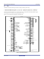
1
User’s Manual
32
R0K572390
SH7239 CPU Board User's Manual
Renesas MCU
SuperHTM RISC engine Family / SH7239 Series
Rev. 1.00
All information contained in these materials, including products and product specifications,
represents information on the product at the time of publication and is subject to change by
Renesas Electronics Corporation without notice. Please review the latest information published by
Renesas Electronics Corporation through various means, including the Renesas Electronics
Corporation website (http://www.renesas.com).
www.renesas.com
Rev. 1.00
Nov. 2010
Notice
1.
2.
3.
4.
5.
6.
7.
All information included in this document is current as of the date this document is issued. Such information, however, is
subject to change without any prior notice. Before purchasing or using any Renesas Electronics products listed herein, please
confirm the latest product information with a Renesas Electronics sales office. Also, please pay regular and careful attention to
additional and different information to be disclosed by Renesas Electronics such as that disclosed through our website.
Renesas Electronics does not assume any liability for infringement of patents, copyrights, or other intellectual property rights
of third parties by or arising from the use of Renesas Electronics products or technical information described in this document.
No license, express, implied or otherwise, is granted hereby under any patents, copyrights or other intellectual property rights
of Renesas Electronics or others.
You should not alter, modify, copy, or otherwise misappropriate any Renesas Electronics product, whether in whole or in part.
Descriptions of circuits, software and other related information in this document are provided only to illustrate the operation of
semiconductor products and application examples. You are fully responsible for the incorporation of these circuits, software,
and information in the design of your equipment. Renesas Electronics assumes no responsibility for any losses incurred by
you or third parties arising from the use of these circuits, software, or information.
When exporting the products or technology described in this document, you should comply with the applicable export control
laws and regulations and follow the procedures required by such laws and regulations. You should not use Renesas
Electronics products or the technology described in this document for any purpose relating to military applications or use by
the military, including but not limited to the development of weapons of mass destruction. Renesas Electronics products and
technology may not be used for or incorporated into any products or systems whose manufacture, use, or sale is prohibited
under any applicable domestic or foreign laws or regulations.
Renesas Electronics has used reasonable care in preparing the information included in this document, but Renesas Electronics
does not warrant that such information is error free. Renesas Electronics assumes no liability whatsoever for any damages
incurred by you resulting from errors in or omissions from the information included herein.
Renesas Electronics products are classified according to the following three quality grades: “Standard”, “High Quality”, and
“Specific”. The recommended applications for each Renesas Electronics product depends on the product’s quality grade, as
indicated below. You must check the quality grade of each Renesas Electronics product before using it in a particular
application. You may not use any Renesas Electronics product for any application categorized as “Specific” without the prior
written consent of Renesas Electronics. Further, you may not use any Renesas Electronics product for any application for
which it is not intended without the prior written consent of Renesas Electronics. Renesas Electronics shall not be in any way
liable for any damages or losses incurred by you or third parties arising from the use of any Renesas Electronics product for an
application categorized as “Specific” or for which the product is not intended where you have failed to obtain the prior written
consent of Renesas Electronics. The quality grade of each Renesas Electronics product is “Standard” unless otherwise
expressly specified in a Renesas Electronics data sheets or data books, etc.
“Standard”:
8.
9.
10.
11.
12.
Computers; office equipment; communications equipment; test and measurement equipment; audio and visual
equipment; home electronic appliances; machine tools; personal electronic equipment; and industrial robots.
“High Quality”: Transportation equipment (automobiles, trains, ships, etc.); traffic control systems; anti-disaster systems; anticrime systems; safety equipment; and medical equipment not specifically designed for life support.
“Specific”:
Aircraft; aerospace equipment; submersible repeaters; nuclear reactor control systems; medical equipment or
systems for life support (e.g. artificial life support devices or systems), surgical implantations, or healthcare
intervention (e.g. excision, etc.), and any other applications or purposes that pose a direct threat to human life.
You should use the Renesas Electronics products described in this document within the range specified by Renesas Electronics,
especially with respect to the maximum rating, operating supply voltage range, movement power voltage range, heat radiation
characteristics, installation and other product characteristics. Renesas Electronics shall have no liability for malfunctions or
damages arising out of the use of Renesas Electronics products beyond such specified ranges.
Although Renesas Electronics endeavors to improve the quality and reliability of its products, semiconductor products have
specific characteristics such as the occurrence of failure at a certain rate and malfunctions under certain use conditions. Further,
Renesas Electronics products are not subject to radiation resistance design. Please be sure to implement safety measures to
guard them against the possibility of physical injury, and injury or damage caused by fire in the event of the failure of a
Renesas Electronics product, such as safety design for hardware and software including but not limited to redundancy, fire
control and malfunction prevention, appropriate treatment for aging degradation or any other appropriate measures. Because
the evaluation of microcomputer software alone is very difficult, please evaluate the safety of the final products or system
manufactured by you.
Please contact a Renesas Electronics sales office for details as to environmental matters such as the environmental
compatibility of each Renesas Electronics product. Please use Renesas Electronics products in compliance with all applicable
laws and regulations that regulate the inclusion or use of controlled substances, including without limitation, the EU RoHS
Directive. Renesas Electronics assumes no liability for damages or losses occurring as a result of your noncompliance with
applicable laws and regulations.
This document may not be reproduced or duplicated, in any form, in whole or in part, without prior written consent of Renesas
Electronics.
Please contact a Renesas Electronics sales office if you have any questions regarding the information contained in this
document or Renesas Electronics products, or if you have any other inquiries.
(Note 1) “Renesas Electronics” as used in this document means Renesas Electronics Corporation and also includes its majorityowned subsidiaries.
(Note 2) “Renesas Electronics product(s)” means any product developed or manufactured by or for Renesas Electronics.
WEEE Directive
Renesas development tools and products are directly covered by the European Union's Waste
Electrical and Electronic Equipment, (WEEE), Directive 2002/96/EC.
As a result, this equipment, including all accessories, must not be disposed of as household
waste but through your locally recognised recycling or disposal schemes.
As part of our commitment to environmental responsibility Renesas also offers to take back the
equipment and has implemented a Tools Product Recycling Program for customers in Europe.
This allows you to return equipment to Renesas for disposal through our approved Producer
Compliance Scheme.
To register for the program, click here "http://www.renesas.com/weee".
This page intentionally left blank.
About This Manual
1. Purpose and Target Readers
This manual is designed to provide the user with an understanding of the functions and operating specifications of this
CPU board. It is intended for users of this CPU board. A basic knowledge of electrical circuits, logical circuits, and
microcomputers (MCUs) is necessary in order to use this manual.
This manual comprises an overview of the CPU board; its function, and operating specifications.
Carefully read all notes in the manual. These notes occur within the body of the text.
The Revision History summarizes primary modifications and additions to the previous versions. Refer to the text of the
manual for details.
The following documents apply to the SH7239 CPU board R0K572390.
Document Type
User’s Manual
Description
Document Title
Describes functions (devices, memory SH7239 CPU Board
maps, electrical characteristics), and
R0K572390 User’s
operating specifications (connectors,
Manual
Document No.
This publication
and switches)
Installation Manual
Describes how to set up hardware
SH7239 CPU Board
and software
R0K572390 Installation
R20UT0298EJ
Manual
The following documents apply to the SH7239 Group. Make sure to refer to the latest versions of these documents. The
newest versions of the documents listed may be obtained from the Renesas Electronics website.
Document Type
User’s manual: Hardware
Description
Document Title
Hardware specifications (pin assignments,
SH7239 Group,
memory maps, peripheral function
SH7237 Group
specifications, electrical characteristics,
User’s manual:
timing charts) and operation description
Hardware
Document No.
R01UH0086EJ
Note: Refer to application notes for details
on using peripheral functions
Software manual
Description of CPU instruction set
SH-2A, SH2A-FPU
REJ09B0051
Software manual
Application note
Applications, sample programs
Available from the Renesas Electronics
Renesas technical update
Product specifications, updates on
website.
documents, etc.
2. Frequently Used Abbreviations and Acronyms
ACIA
Asynchronous Communication Interface Adapter
bps
bits per second
CRC
Cyclic Redundancy Check
DMA
Direct Memory Access
DMAC
Direct Memory Access Controller
GSM
Global System for Mobile Communications
Hi-Z
High Impedance
IEBus
Inter Equipment bus
I/O
Input/Output
IrDA
Infrared Data Association
LSB
Least Significant Bit
MSB
Most Significant Bit
NC
Non-Connection
PLL
Phase Locked Loop
PWM
Pulse Width Modulation
SFR
Special Function Registers
SIM
Subscriber Identity Module
UART
Universal Asynchronous Receiver/Transmitter
VCO
Voltage Controlled Oscillator
All trademarks and registered trademarks are the property of their respective owners.
Table of Contents
1. Overview....................................................................................................................................................... 1-1
1.1
Introduction ..................................................................................................................................................... 1-1
1.2
Configuration................................................................................................................................................... 1-2
1.3
Board Specifications ........................................................................................................................................ 1-3
1.4
Exterior ............................................................................................................................................................ 1-4
1.5
Block Diagram................................................................................................................................................. 1-5
1.6
Component Layout .......................................................................................................................................... 1-6
1.7
Memory Maps.................................................................................................................................................. 1-8
1.8
Absolute Maximum Ratings .......................................................................................................................... 1-10
1.9
Operating Conditions..................................................................................................................................... 1-10
2. Functions ...................................................................................................................................................... 2-1
2.1
Overview of Functions..................................................................................................................................... 2-1
2.2
CPU ................................................................................................................................................................. 2-2
2.3
External Memory ............................................................................................................................................. 2-3
2.3.1
SRAM..................................................................................................................................................... 2-3
2.3.2
EEPROM ................................................................................................................................................ 2-5
2.4
Serial Port Interface ......................................................................................................................................... 2-6
2.5
I/O Ports........................................................................................................................................................... 2-7
2.6
RCAN Interface ............................................................................................................................................. 2-11
2.7
LCD Interface ................................................................................................................................................ 2-12
2.8
H-UDI Interface............................................................................................................................................. 2-13
2.9
Switches and Jumpers.................................................................................................................................... 2-14
2.10
LEDs and Potentiometer................................................................................................................................ 2-15
2.11
Power Module................................................................................................................................................ 2-16
2.12
Clock Module ................................................................................................................................................ 2-17
2.13
Reset Module ................................................................................................................................................. 2-18
3. Operating Specifications............................................................................................................................... 3-1
3.1
Connectors ....................................................................................................................................................... 3-1
3.1.1
Application Headers (JA1, JA2, JA3, JA5, JA6).................................................................................... 3-2
3.1.2
Common Ring Connectors (J1, J2, J3, J4).............................................................................................. 3-9
3.1.3
DC Power Jack (J5) .............................................................................................................................. 3-12
3.1.4
H-UDI Port Connectors (J6 and J7)...................................................................................................... 3-13
3.1.5
Serial Port Connector (J8)..................................................................................................................... 3-15
3.1.6
RCAN Port Connector (J9)................................................................................................................... 3-16
3.1.7
LCD Interface Connector (J10) ............................................................................................................ 3-17
3.1.8
External Power Supply Connectors (J11, J12, J13) .............................................................................. 3-18
3.2
Operating Components .................................................................................................................................. 3-19
3.2.1
Jumpers (JP1, JP2, JP3) ........................................................................................................................ 3-20
3.2.2
Switches................................................................................................................................................ 3-21
3.2.3
Potentiometer........................................................................................................................................ 3-22
3.2.4
LEDs..................................................................................................................................................... 3-22
3.3
Dimensions .................................................................................................................................................... 3-22
Appendix R0K572390 Schematics .......................................................................................................................1
SH7239 CPU Board R0K572390
1. Overview
1. Overview
1.1
Introduction
The R0K572390 is a CPU board designed for evaluating the features and performance of the SH7239 Group of Renesas
Electronics single-chip RISC microcomputers (MCUs). It is also used for developing and evaluating application software
for these MCUs. The R0K572390 CPU board lineup consists of following two models:
•
•
R0K572390C000BR, which includes SH7239A MCU (3.3 V, working at 160 MHz)
R0K572390C020BR, which includes SH7239B MCU (5.0 V, working at 100 MHz)
The SH7239 MCU’s internal peripheral pins are connected to common ring connectors and application headers on the
R0K572390 to allow for timing evaluation with peripherals using measurements instruments, and the development of the
expansion board according to its application. The Renesas Electronics E10A-USB on-chip emulator can be connected to
the R0K572390.
R20UT0297EJ0100 Rev. 1.00
Nov. 08, 2010
1-1
SH7239 CPU Board R0K572390
1.2
1. Overview
Configuration
Figure 1.1 shows an example of a system configuration using the R0K572390.
Application headers
AC adapter
provided with the
CPU board
Serial port
Character
LCD
RCAN
port
SH7239 CPU board
R0K572390
SH7239
H-UDI port connector
(14-pin or 38-pin)
E10A-USB emulator (1)
Application headers
High-performance
Embedded Workshop (1)
SuperH RISC engine (1)
C/C++ compiler package
USB
Host computer
(1)
Note: 1. These items are not included in this CPU board, and must be prepared by user.
Figure 1.1 Configuration Using the R0K572390
R20UT0297EJ0100 Rev. 1.00
Nov. 08, 2010
1-2
SH7239 CPU Board R0K572390
1.3
1. Overview
Board Specifications
Table 1.1 lists the specifications of the R0K572390.
Table 1.1 R0K572390 Board Specifications
Item
CPU
Description
SH7239A
(1)
or SH7239B
(2)
•
Input (XIN) clock: 10 MHz (1) or 12.5 MHz (2)
•
CPU clock: Up to 160 MHz
•
Peripheral clock: Up to 40 MHz
•
Internal memory
(1)
or 100 MHz (2)
(1)
or 50 Hz (2)
Flash memory: 512 KB
RAM: 64 KB
FLD (flash memory to store data): 32 KB
Memory
Connectors
LEDs, potentiometer
Switches, jumpers
•
EEPROM: 64 KB (SPI interface)
•
SRAM: 64 KB (8-bit bus × 2, optional)
•
Common ring connectors (All CPU signals, optional)
•
Application headers (Bus, I/O, VCC, GND, optional)
•
Serial port connector (D-sub, 9-pin)
•
RCAN port connector (3-pin, pin header)
•
14-pin LCD interface connector
•
14-pin H-UDI port connector
•
38-pin H-UDI port connector
•
Power LED: 1
•
Boot mode LED: 1
•
User LEDs: 4
•
10-kΩ potentiometer: 1
•
Reset switch: 1
•
User switches: 3 (NMI, IRQ3 or ADTRG, IRQ4)
•
Mode setting DIP switches: 1 (2/package)
•
Power select jumper: 1 (Not populated)
•
RCAN signal connection jumper: 1 (Not populated)
•
Board specifications
Notes 1.
2.
3.
4.
(3)
_____________
(4)
_____________
ADTRG signal connection jumper: 1 (Not populated)
•
Dimensions: 100 mm × 120 mm
•
Mounting form: 4-layer, double-sided
•
Number of boards: 1
These parameters apply to the R0K572390C000BR.
These parameters apply to the R0K572390C020BR.
User is allowed to install SRAM on the R0K572390C000BR.
Power supply voltage is fixed to 3.3 V on the R0K572390C000BR, 5 V on the R0K572390C020BR.
R20UT0297EJ0100 Rev. 1.00
Nov. 08, 2010
1-3
SH7239 CPU Board R0K572390
1.4
1. Overview
Exterior
Figure 1.2 shows the exterior of the R0K572390.
Figure 1.2 R0K572390 Exterior
R20UT0297EJ0100 Rev. 1.00
Nov. 08, 2010
1-4
SH7239 CPU Board R0K572390
1.5
1. Overview
Block Diagram
Figure 1.3 shows the block diagram of the R0K572390.
RCAN port
connector
38-pin H-UDI
port connector
14-pin H-UDI
port connector
Serial port
connector
H-UDI
SCI ch2
AUD
RCAN
5 V to 3.3 V
3.3 V to 5 V
Optional
PORT
LCD
interface
connector
SH7239
(1)
10 MHz
or 12.5 MHz (2)
Power
select
jumper
RSPI
160 MHz (1)
or 100 MHz (2)
Crystal unit
5V
SH7239 CPU board
R0K572390
3.3 V (1)
or 5 V (2)
EEPROM
64 KB
SRAM
64 KB (1)
16-bit
8- or 16-bit
External bus 40 MHz (max.) (1)
3.3 V
8- or 16-bit
DC-DC
Common ring connectors (optional)
and Application headers (optional)
Notes:
1. These are applicable to the R0K572390C000BR.
2. These are applicable to the R0K572390C020BR.
Figure 1.3 R0K572390 Block Diagram
R20UT0297EJ0100 Rev. 1.00
Nov. 08, 2010
1-5
SH7239 CPU Board R0K572390
1.6
1. Overview
Component Layout
Figure 1.4 shows the layout of the major components on the R0K572390.
Character LCD
(accessory)
Top view of the component side
X1
SH7239
Top view of the solder side
J4
SRAM (optional)
Figure 1.4 R0K572390 Component Layout
R20UT0297EJ0100 Rev. 1.00
Nov. 08, 2010
1-6
SH7239 CPU Board R0K572390
1. Overview
Table 1.2 lists the major components on the R0K572390.
Table 1.2 Major Components on the R0K572390
Symbol
Name
Remarks
Recommended Optional Components
(Manufacturer Name and Part Number)
U1
CPU
SH7239A
(1)
(Renesas)
SH7239B
(2)
(Renesas)
(3)
U2, U3
SRAM
Optional
U4
EEPROM
R1EX25512ATA00A (Renesas)
M5M5256DVP-70G (Renesas)
U13
RS-232C transceiver
MAX3222CPWR (TI)
U11
RCAN transceiver
HA13721RPJE (Renesas)
U14
3.3 V regulator
LM2738-YMY 550kHz (NS)
U6
Reset IC
M51957BFP (Renesas)
X1
Crystal unit
CXZ49GFB10000H0PESZZ
(1)
CXZ49GFB12500H0PESZZ
(2)
(Kyocera Kinseki)
J1 to J4
Common ring connectors
Optional
18-pin double row pin header
JA1, JA2
JA3
Application headers
Optional
13-pin double row pin header
Application header
Optional
25-pin double row pin header
JA5, JA6
Application headers
Optional
12-pin double row pin header
J5
DC power jack
KLDX-SMT2-0202-A (Kycon)
J6
14-pin H-UDI port connector
HTST-107-01-T-DV (Samtec)
J7
38-pin H-UDI port connector
2-5767004-2 (Tyco electronics)
J8
Serial port connector
154188 (ERNI)
J9
RCAN port connector
B3P-SHF-1AA(LF)(SN) (J.S.T.)
J10
LCD interface connector
SSM-107-LM-DV-P-TR (Samtec)
J11
External power supply connector
Optional
A2-2PA-2.54DSA (Hirose)
J12
External power supply connector
Optional
A2-2PA-2.54DSA (Hirose)
J13
External power supply connector
Optional
A2-2PA-2.54DSA (Hirose)
POWER
Power LED
Green
BOOT
Boot mode LED
Orange
LED0 to LED3
User LEDs
Green, orange, red, red
VR1
Potentiometer
CT-6ETV10KΩ (NIDEC Copal)
RESET
Reset switch
B3S-1000 (OMRON)
SW1
NMI switch
B3S-1000 (OMRON)
SW2, SW3
IRQ3, IRQ4 switches
B3S-1000 (OMRON)
SW4
Mode setting DIP switches (2/package)
A6HF-2102 (OMRON)
JP1
Power select jumper
Optional
2.54 mm pitch 3-way pin header
JP2
RCAN signal connection jumper
Optional
2.54 mm pitch 2-way pin header
JP3
_____________
Optional
2.54 mm pitch 2-way pin header
Notes: 1.
2.
3.
4.
A D T R G signal connection jumper
These parameters apply to the R0K572390C000BR.
These parameters apply to the R0K572390C020BR.
User is allowed to install SRAM on the R0K572390C000BR only.
Power supply voltage is fixed to 3.3 V on the R0K572390C000BR, 5 V on the R0K572390C020BR.
R20UT0297EJ0100 Rev. 1.00
Nov. 08, 2010
1-7
SH7239 CPU Board R0K572390
1.7
1. Overview
Memory Maps
Figure 1.5 and Figure 1.6 show memory map examples of the SH7239 and R0K572390.
SH7239 Logic Space
in MCU Mode 3
(Single-chip Mode)
H'0000 0000
R0K572390 Memory Map
Internal ROM (512 KB)
Reserved
H'0000 0000
H'0008 0000
H'0008 0000
Internal ROM (512 KB)
Reserved
H'0040 2000
H'0040 4000
FCU firmware area (8 KB)
H'0040 2000
H'0040 4000
FCU firmware area (8 KB)
Reserved
H'800F FFFF
H'8010 0000
Data flash (32 KB)
Reserved
H'800F FFFF
H'8010 0000
Reserved
H'80FF 7FFF
H'80FF 8000
H'80FF A000
FCURAM (8 KB)
Reserved
H'80FF 7FFF
H'80FF 8000
H'80FF A000
Reserved
H'FFF7 FFFF
H'FFF8 0000
H'FFF8 8000
H'FFF9 0000
Data flash (32 KB)
H'8010 8000
H'8010 8000
Internal RAM (32 KB)
Reserved
Internal RAM (32 KB)
FCURAM (8 KB)
Reserved
H'FFF7 FFFF
H'FFF8 0000
H'FFF8 8000
H'FFF9 0000
Internal RAM (32 KB)
Reserved
Internal RAM (32 KB)
H'FFF9 8000
H'FFF9 8000
Reserved
Reserved
H'FFFD FFFF
H'FFFE 0000
H'FFFD FFFF
H'FFFE 0000
Peripheral I/O
Peripheral I/O
H'FFFF FFFF
H'FFFF FFFF
Figure 1.5 SH7239 Memory Map Example (MCU Mode 3)
R20UT0297EJ0100 Rev. 1.00
Nov. 08, 2010
1-8
SH7239 CPU Board R0K572390
1. Overview
SH7239 Logic Space in
MCU Mode 2
(Internal ROM Enabled Mode)
H'0000 0000
R0K572390 Memory Map
H'0000 0000
H'0008 0000
Internal ROM (512 KB)
Reserved
H'0008 0000
Internal ROM (512 KB)
Reserved
H'0040 2000
H'0040 4000
FCU firmware area (8 KB)
H'0040 2000
H'0040 4000
FCU firmware area (8 KB)
Reserved
H'0200 0000
CS0 space
H'0220 0000
Reserved
H'0400 0000
CS1 space
H'0420 0000
H'0200 0000
H'0201 0000
H'0220 0000
H'0400 0000
H'0BFF FFFF
H'0C00 0000
CS3 space
H'0C20 0000
Reserved
H'1000 0000
CS4 space
H'1020 0000
Reserved
H'1400 0000
CS5 space
H'1420 0000
Reserved
H'1800 0000
CS6 space
H'1820 0000
H'0BFF FFFF
H'0C00 0000
H'0C20 0000
H'1000 0000
H'1020 0000
H'1400 0000
H'1420 0000
H'1800 0000
Data Flash (32 KB)
H'800F FFFF
H'8010 0000
Reserved
Not used
Reserved
Not used
Reserved
Not used
Data Flash (32 KB)
H'8010 8000
FCURAM (8 KB)
Reserved
H'80FF 7FFF
H'80FF 8000
H'80FF A000
Internal RAM (32 KB)
Reserved
Internal RAM (32 KB)
H'FFF9 8000
FCURAM (8 KB)
Reserved
Reserved
H'FFF9 0000
Not used
Reserved
Reserved
H'FFF8 8000
Not used
H'1820 0000
H'8010 8000
H'FFF7 FFFF
H'FFF8 0000
Not used
Reserved
Reserved
Reserved
H'80FF 7FFF
H'80FF 8000
H'80FF A000
(1)
H'0420 0000
Reserved
H'800F FFFF
H'8010 0000
Reserved
SRAM (64 KB)
H'FFF7 FFFF
H'FFF8 0000
H'FFF8 8000
H'FFF9 0000
Internal RAM (32 KB)
Reserved
Internal RAM (32 KB)
H'FFF9 8000
Reserved
Reserved
H'FFFD FFFF
H'FFFE 0000
H'FFFD FFFF
H'FFFE 0000
Peripheral I/O
Peripheral I/O
H'FFFF FFFF
H'FFFF FFFF
Note: 1. SRAM is optional. User is allowed to install it on the R0K572390C000BR only.
Figure 1.6 SH7239 Memory Map (MCU Mode 2, for R0K572390C000BR only)
R20UT0297EJ0100 Rev. 1.00
Nov. 08, 2010
1-9
SH7239 CPU Board R0K572390
1.8
1. Overview
Absolute Maximum Ratings
Table 1.3 lists the absolute maximum ratings of the R0K572390.
Table 1.3 R0K572390 Absolute Maximum Ratings
Symbol
Item
Value
Remarks
5 V system power supply voltage
−0.3 to 6.0 V
Reference voltage: VSS
3.3 V system power supply voltage
−0.3 V to 4.0 V
Reference voltage: VSS
AVCC
5 V system analog power supply
voltage
−0.3 V to 6.0 V
Reference voltage: AVSS
Topr
Operating ambient temperature (2)
0°C to 50°C
Do not expose to condensation or corrosive gas
Tstg
Storage ambient temperature (2)
−10°C to 60°C
Do not expose to condensation or corrosive gas
5VCC
3VCC
(1)
Notes: 1. 3VCC is used to supply the 3.3 V system power supply voltage directly from the external power supply
connector.
2. Ambient temperature refers to the air temperature in the vicinity of the board.
1.9
Operating Conditions
Table 1.4 lists the operating conditions for the R0K572390.
Table 1.4 R0K572390 Operating Conditions
Symbol
5VCC
Item
Value
Remarks
5 V system power supply voltage
4.75 V to 5.25 V
Reference voltage: VSS
3.3 V system power supply voltage
3.15 V to 3.45 V
Reference voltage: VSS
AVCC
5 V system analog power supply
voltage
4.75 V to 5.25 V
Reference voltage: AVSS
Topr
Maximum current consumption
1 A max.
Both 5 V system power supply (including
analog), and 3.3 V system power supply
Tstg
Operating ambient temperature (2)
0°C to 50°C
Do not expose to condensation or corrosive gas
3VCC
(1)
Notes: 1. 3VCC is used to supply the 3.3 V system power supply voltage directly from the external power supply
connector.
2. Ambient temperature refers to the air temperature in the vicinity of the board.
R20UT0297EJ0100 Rev. 1.00
Nov. 08, 2010
1-10
SH7239 CPU Board R0K572390
2. Functions
2. Functions
2.1
Overview of Functions
The R0K572390 includes the function modules listed in the following table.
Table 2.1 R0K572390 Function Modules
Section
2.2
Function
CPU
Description
SH7239A
(1)
or SH7239B
(2)
•
Input (XIN) clock: 10 MHz (1) or 12.5 MHz (2)
•
CPU clock: Up to 160 MHz
•
Peripheral clock: Up to 40 MHz
•
Internal memory
(1)
or 100 MHz (2)
(1)
or 50 Hz (2)
Flash memory: 512 KB
RAM: 64 KB
FLD (flash memory to store data): 32 KB
2.3
External Memory
•
EEPROM: 64 KB (SPI interface)
•
SRAM: 64 KB (8-bit bus × 2, optional)
(3)
2.4
Serial Port Interface
Connects the SH7239 SCI channel 2 to the serial port connector
2.5
I/O Ports
Connects all the SH7239 signals to common ring connectors
Connects the SH7239 bus and I/O ports to application headers
2.6
RCAN Interface
Connects the SH7239 RCAN pins to the RCAN port connector via the RCAN
transceiver
2.7
LCD Interface
Character LCD interface
2.8
H-UDI Interface
Connects the SH7239 H-UDI/AUD pins to the H-UDI port connectors (14-pin,
38-pin) to enable debugging the R0K572390 using the E10A-USB emulator
(4)
2.9
Switches and Jumpers
•
Reset switch
•
User switches: 3 (Connects NMI, IRQ3 or ADTRG, and IRQ4 pins)
•
Mode setting DIP switches: 1 (2/package)
•
Power select jumper: 1 (Not populated)
•
•
2.10
LEDs and Potentiometer
_____________
RCAN signal connection jumper: 1 (Not populated)
_____________
ADTRG signal connection jumper: 1 (Not populated)
•
Power LED: 1
•
Boot mode LED: 1
•
User LEDs: 4
•
10-kΩ potentiometer: 1
2.11
Power Module
Controls the R0K572390 system power supply
2.12
Clock Module
Clock source: 10 MHz (1) or 12.5 MHz (2) crystal unit
2.13
Reset Module
Resets the devices installed on the R0K572390
–
Operating Specifications
Refer to chapter 3 for details on connectors, switches, LEDs, and the
potentiometer
Notes 1.
2.
3.
4.
These parameters apply to the R0K572390C000BR.
These parameters apply to the R0K572390C020BR.
User is allowed to install SRAM on the R0K572390C000BR.
_____
H-UDI port connector cannot be used when using addresses A16 to A20, and AH by the application headers.
R20UT0297EJ0100 Rev. 1.00
Nov. 08, 2010
2-1
SH7239 CPU Board R0K572390
2.2
2. Functions
CPU
The R0K572390 includes following two models according to the MCU product lineup.
•
•
R0K572390C000BR: SH7239A MCU (3.3 V, CPU clock = 160 MHz max, peripheral clock = 40 MHz max)
R0K572390C020BR: SH7239B MCU (5.0 V, CPU clock = 100 MHz max, peripheral clock = 50 MHz max)
The SH7239A and SH7239B MCUs have 512 KB of flash memory, 32 KB of FLD, and 64 KB of RAM to support
various applications such as data processing and equipment control.
Figure 2.1 shows the SH7239 block diagram on the R0K572390.
SH7239
86
Clock
84
26
88
System
control
87
1
16
17
18
19
9
10
20
21
GPIO
22
3
11
12
13
14
2
Serial port connector
8
98
99
100
101
106
107
108
109
A/D
112
113
114
115
116
117
118
119
6
7
91
92
66
67
H-UDI port connector
47
48
51
52
53
95
Mode
setting
DIP
switches
94
120
PC0/A0/POE0/IRQ4
EXTAL
PC1/A1/ADRTG
XTAL
PC2/A2
PA18/CK
PC3/A3
RES
PC4/A4
NMI
PC5/A5
WDTOVF
PC6/A6
PC7/A7
PE0/TIOC0A/TIOC4AS/DREQ0
PC8/A8/CRx0/RXD0/POE4
PE1/TIOC0B/TIOC4BS/TEND0
PC9/A9/CTx0/TXD0/SCK0
PE2/TIOC0C/TIOC4CS/DREQ1
PC10/A10/TIOC1A/CRx0/RXD0
PE3/TIOC0D/TIOC4DS/TEND1
PC11/A11/TIOC1B/CTx0/TXD0
PE9/TIOC3B/DACK2
PC12/A12/TCLKA
PE11/TIOC3D/DACK3
PC13/A13/IRQ0/TCLKB
PE4/TIOC1A/SCK3/POE8/IRQ4
PC14/A14/IRQ1/TCLKC
PE5/TIOC1B/TIOC3BS/TXD3
PC15/A15/IRQ2/TCLKD
PE6/TIOC2A/TIOC3DS/RXD3
PE8/TIOC3A/DREQ2/SCK2/SSL2
PD0/D0
PE12/TIOC4A
PD1/D1
PE13/TIOC4B/MRES
PD2/D2/TIC5U/RXD2
PE14/DACK0/TIOC4C
PD3/D3/TIC5V/TXD2
PD4/D4/TIC5W/SCK2
PE15/DACK1/TIOC4D/IRQOUT
PE7/TIOC2B/UBCTRG/RXD2/SSL1
PD5/D5/TIC5US
PE10/TIOC3C/DREQ3/TXD2/SSL3
PD6/D6/TIC5VS
PD7/D7/TIC5WS
PF0/AN0
PD8/D8/TIOC3AS/AUDATA0
PF1/AN1
PD9/D9/TIOC3CS/AUDATA1
PF2/AN2
PD10/D10/TIOC3BS/AUDATA2
PF3/AN3
PD11/D11/TIOC3DS/AUDATA3
PF4/AN4
PD12/D12/TIOC4AS/AUDSYNC
PF5/AN5
PD13/D13/TIOC4BS/AUDCK
PF6/AN6
PD14/D14/TIOC4CS
PF7/AN7
PD15/D15/TIOC4DS
PF8/AN8
PA17/RD
PF9/AN9
PF10/AN10
PA16/WRL
PF11/AN11
PA15/WRH
PF12/AN12
PF13/AN13
PA0/RXD0/CS0/CRx0/IRQ4
PF14/AN14
PA1/TXD0/CS1/CTx0/IRQ5
PF15/AN15
PA9/IRQ3/TCLKD/CS3/SSL0/SCK0
PB16/AUDSYNC
PA8/IRQ4/TCLKC/CS4/MISO/RXD1
PB17/AUDCK
PA7/IRQ5/TCLKB/CS5/MOSI/TXD1
PB18/AUDATA2
PA6/IRQ6/TCLKA/CS6/RSPCK/SCK1
29
30
Switch
31
32
33
Character LCD
34
35
36
39
Address bus (1)
40
41
42
43
44
45
46
56
67
68
69
60
61
62
63
68
Data bus
(1)
69
70
71
72
73
74
75
23
27
Bus control (1)
28
82
83
RCAN port connector
78
79
80
EEPROM
(RSPI)
81
PB19/AUDATA3
PB20/AUDATA0
PB21/AUDATA1
PB0/A16/IRQ0/TIOC2A/TMS
PB1/A17/IRQOUT/ADTRG/TIOC0A/IRQ1/TRST
PB2/A18/IRQ2/RXD3/TIOC0B/BACK/TDI
PB3/A19/IRQ3/TXD3/TIOC0C/BREQ/AH/TDO
PB4/A20/IRQ4/SCK3/TIOC0D/WAIT/BACK/BS/TCK
ASEMD0
FWE/ASEBRKAK/ASEBRK
MD0
Note 1: External bus can be used on the
SH7239A only.
Figure 2.1 SH7239 Block Diagram
R20UT0297EJ0100 Rev. 1.00
Nov. 08, 2010
2-2
SH7239 CPU Board R0K572390
2.3
External Memory
2.3.1
SRAM
2. Functions
64-KB SRAM (32-Kword × 8-bit × 2) can be
installed on the R0K572390 (SRAM is optional, and not installed by
_______
default). The SH7239 Bus State _______
Controller CS0 controls the SRAMs. The SRAM can be used only when setting the
SH7239A in MCU mode 2. As CS0 signal to control SRAM is also used as the RCAN CRx0, RCAN and SRAM cannot
be used at the same time. When using SRAM, remove the resistor R41 and install the resistor R30 (not installed by
default), and connect the signal to SRAM.
Figure 2.2 shows the SH7239 and SRAM configuration.
VCC
SRAM
(M5M5256DVP-70G, 32-Kword × 8-bit)
SH7239
46 to 39, 36 to 30
PC15/A15/IRQ2/TCLKD to PC1/A1/ADRTG
15
A14 to A0
82
PA0/RXD0/CS0/CRx0/IRQ4
S
23
PA17/RD
OE
27
PA16/WRL
W
28
PA15/WRH
75 to 68, 63 to 56
PD15/D15/TIOC4DS to PD0/D0
16
D7 to D0
8
DQ8 to DQ1
SRAM
(M5M5256DVP-70G, 32-Kword × 8-bit)
A14 to A0
S
OE
W
D15 to D8
8
DQ8 to DQ1
Application header (JA1)
Following signals are connected to JA1:
PC1/A1/ADTRG
1
PC4/A4 to PC11/A11/TIOC1B/CTx0/TXD0
8 15 to 22
8
PC13/A13/IRQ0/TCLKB
1
PC14/A14/IRQ1/TCLKC
1
9
PC15/A15/IRQ2/TCLKD
1
23
PC12/A12/TCLKA
1
25
PC13/A13/IRQ0/TCLKB
1
26
7
15 16 to 2
PC15/A15/IRQ2/TCLKD to PC1/A1/ADTRG
PA0/RXD0/CS0/CRx0/IRQ4
45
PA17/RD
25
PA16/WRL
48
PA15/WRH
47
36 to 17
16
IRQ1
IRQ2
TCLKA
TCLKB
A15 to A1
CS0
RD
WRL
WRH
D15 to D0
Application header (JA5)
Following signals are connected to JA5
PA0/RXD0/CS0/CRx0/IRQ4
6
PC8/A8/CRx0/RXD0/POE4
1
16
PC14/A14/IRQ1/TCLKC, PC15/A15/IRQ2/TCLKD
2
17, 18
11
11 to 15, 19 to 24
3
14 to 16
CRx0
M2_POE
M2-related signal (CLK)
M2-related signal
Application header (JA6)
Following signals are connected to JA6
PD4/D4/TIC5W/SCK2
IRQ0
Application header (JA3)
Following signals are connected to JA3
PD15/D15/TIOC4DS to PD5/D5/TIC5US
IOPort_0 to IOPort_7
Application header (JA2)
Following signals are connected to JA2
PD15/D15/TIOC4DS to PD0/D0
ADTRG
to PD2/D2/TIC5U/RXD2
Note: Zero-ohm resistors to select signals are not indicated.
M1-related signal
Figure 2.2 SRAM Configuration
R20UT0297EJ0100 Rev. 1.00
Nov. 08, 2010
2-3
SH7239 CPU Board R0K572390
2. Functions
Figure 2.3 shows SRAM read/write timing chart. Table 2.2 lists the Bus State Controller settings.
25 ns
CK
A15 to A1
CS0
RD
WRL, WRH
D15 to D0
Read data
Write data
This is an example when bus clock is at 40 MHz.
Figure 2.3 SRAM Read/Write Timing Chart
Table 2.2 Bus State Controller Settings
User Area
CS0
Target Device
M5M5256DVP-70G
Setting
CS0 space bus control register (CS0BCR):
Recommended value: H'0240 0400
⎯ Number of idles between Read-Write cycles:
IWRWD [2:0] = IWRWS [2:0] = B'001; 1 idle cycle inserted
⎯ Memory:
TYPE [2:0] = B'000; normal space
⎯ Data bus width: BSZ [1:0] = B'10; 16-bit bus
CS0 space wait control register (CS0WCR):
Recommended value: H'0000 0940
⎯
_______
_____
_________
Number of delay cycles from address, CS0 assertion to RD, WRxx
assertion:
SW [1:0] = B'01; 1.5 cycles
⎯ Number of access wait cycles:
WR [3:0] = B'0010; 2 cycles
⎯ External wait mask specification:
WM = B'1; Ignore external wait input
_____
_________
_______
⎯ Number of delay cycles from RD, WRxx, negation to address, CS0
negation:
HW [1:0] = B'00; 0.5 cycles
R20UT0297EJ0100 Rev. 1.00
Nov. 08, 2010
2-4
SH7239 CPU Board R0K572390
2.3.2
2. Functions
EEPROM
The R0K572390 includes a 64-KB EEPROM (64-Kword × 8-bit). The SH7239 Renesas Serial Peripheral Interface
controls the EEPROM. Pins to control EEPROM are also connected to the user switch
SW2, and
application headers
_______
_______
(JA1, JA2, and JA3) to be multiplexed with SCI channel 1 pin, MTU2 pins, IRQ3, CS3, and CS6 signals. Note that
these signals cannot be used at the same time. Figure 2.4 shows the SH7239 and EEPROM configuration.
VCC
EEPROM
(R1EX25512ATA00A,
64-Kword × 8-bit)
SH7239
PA9/IRQ3/TCLKD/CS3/SSL0/SCK0
PA8/IRQ4/TCLKC/CS4/MISO/RXD1
PA7/IRQ5/TCLKB/CS5/MOSI/TXD1
PA6/IRQ6/TCLKA/CS6/RSPCK/SCK1
78
S
79
Q
80
D
81
C
W
HOLD
Not installed
VSS
Application header (JA1)
23
IRQ3
Application header (JA2)
8
6
10
21
22
Switch module
IRQ3
SCIaRX
SCIaTX
SCIaCK
TCLKA
TCLKB
Application header (JA3)
27
28
CSa
CSb
Note: Zero-ohm resistors to select signals are not indicated.
Figure 2.4 EEPROM Configuration
R20UT0297EJ0100 Rev. 1.00
Nov. 08, 2010
2-5
SH7239 CPU Board R0K572390
2.4
2. Functions
Serial Port Interface
On the R0K572390, SH7239 SCI channel 2 is connected to the serial port connector (J8) via the RS-232C transceiver.
Also, the SH7239 SCI channel 2 is connected to pins 7 and 8 of the application header (JA6), pin 11 (used as the
TIOC3C) of the application header (JA2). Install zero-ohm resistor in appropriate pin to connect pins 5 and 6 of the
application header (JA6) to the serial port connector (J8) via the RS-232C transceiver. When using the SH7239 SCI
channel 2 as the serial port, it cannot be used as the application header.
To use the serial port connector (J8) in boot mode, remove zero-ohm resistors R59 and R60 to connect signals PE10 and
PE7 between the RS-232C transceiver and the SH7239. Then, install zero-ohm resistors R166 and R167 (not installed by
default) to connect signals PB3 and PB2 between the RS-232C transceiver and the SH7239. Note that the H-UDI port
connector cannot be used.
Figure 2.5 shows the serial port block diagram.
VCC
SH7239
PE10/TIOC3C/DREQ3/TXD2/SSL3
22 kΩ
Serial port connector
(J8)
22 kΩ
RS-232C
transceiver
R59 0 Ω
8
VCCQ
PE7/TIOC2B/UBCTRG/RXD2/SSL1
R56 0 Ω
R61
Not
R166
installed
R63
R60 0 Ω
R65
0Ω
VSS
R167
Not
installed
5
6
8
7
PB2/A18/IRQ2/RXD3/TIOC0B/BACK/TDI
H-UDI port connector block
Not installed when using a socket with the
straight cable
Not installed when using a plug with the
crossover cable (default)
RS232TX
RS232RX
SCIbTX
SCIbRX
Male plug with the
crossover cable
GND
5
4
52
3
51
Application header (JA2)
VCC
11
R66 0 Ω
VSS
Application header (JA6)
PB3/A19/IRQ3/TXD3/TIOC0C/BREQ/AH/TDO
R49 0 Ω
R55
R58
22 kΩ
×2
2
R54 0 Ω
0Ω×4
2
1
Female socket with the
straight cable
1
9
2
8
3
7
4
6
GND
5
6
7
8
9
M1_UD
10 kΩ × 2
TDO
TDI
Note: Some zero-ohm resistors to select signals are not indicated.
• To use the Serial port connector (J8) in boot mode
Remove zero-ohm resistors (R59 and R60) connecting signals PE10 and PE7 between the RS-232C transceiver and the SH7239.
Then, install zero-ohm resistors (R166 and R167, not installed by default) to connect signals PB3 and PB2. Note that the H-UDI port connector cannot be used.
Figure 2.5 Serial Port Block Diagram
R20UT0297EJ0100 Rev. 1.00
Nov. 08, 2010
2-6
SH7239 CPU Board R0K572390
2.5
2. Functions
I/O Ports
All SH7239 signals are connected to common ring connectors on the R0K572390. Most of the I/O ports are connected to
application headers. Table 2.3 to Table 2.6 list I/O port functions. Some I/O ports are also connected to devices, I/O
connectors, switches and LEDs. For details, refer to chapter 3 Operating Specifications.
Table 2.3 I/O Port Functions (1/4)
SH7239
No.
Common ring
connector
Pin Name
J1
J2
J3
Application header
J4
JA1
JA2
JA3
JA5
JA6
_____________
1
Function
_____________
WDTOVF
1
[5]
WDTOVF
_____________
2
PE7/TIOC2B/UBCTRG/RXD2/SSL1
2
(7)
RXD2
3
PE8/TIOC3A/SCK2/DREQ2/SSL2
3
(10),
SCK2, TIOC3A
[13]
4
VCC
4
5
VSS
6
PB16/AUDSYNC
5
6
7
PB17/AUDCK
7
8
PE10/TIOC3C/TXD2/DREQ3/SSL3
8
[11]
9
PE9/TIOC3B/DACK2
9
13
TIOC3B
10
PE11/TIOC3D/DACK3
10
14
TIOC3D
11
PE12/TIOC4A
11
15
TIOC4A
TIOC4B
______________
(8)
TIOC3C, TXD2
_________
12
PE13/TIOC4B/MRES
12
17
13
PE14/DACK0/TIOC4C
13
[16]
14
PE15/DACK1/TIOC4D/IRQOUT
14
18
15
VSS
15
16
PE0/TIOC0A/TIOC4AS/DREQ0
16
17
PE1/TIOC0B/TIOC4BS/TEND0
17
(9)
(9)
18
PE2/TIOC0C/TIOC4CS/DREQ1
18
(23)
(10)
19
PE3/TIOC0D/TIOC4DS/TEND1
19
(2)
TIOC4C,
DACK0
_____________
(23)
TIOC4D
(7)
(1)
TIOC0A,
DREQ0
(3)
TIOC0B,
TEND0
TIOC0C
(14)
[16]
TIOC0D
[9],
(11),
(12)
(14)
TIOC1A, IRQ4,
SCK3
_________
20
PE4/TIOC1A/SCK3/POE8/IRQ4
20
(23)
21
PE5/TIOC1B/TIOC3BS/TXD3
21
[19]
22
PE6/TIOC2A/TIOC3DS/RXD3
22
[20]
(13)
(9)
TIOC1B, TXD3
(12)
TIOC2A, RXD3
(15)
_____
23
PA17/RD
24
VCL
25
VSS
26
PA18/CK
_____
23
25
RD
26
[44]
CK
27
48
WRL
28
47
WRH
25
_______
27
PA16/WRL
_______
_______
28
PA15/WRH
_______
Notes: 1. Brackets [ ] indicate the signals connected to the CPU pin via a device, and zero-ohm resistor (installed).
2. Parentheses ( ) indicate the signals connected to the CPU pin via zero-ohm resistor (NOT installed). Remove
or install zero-ohm resistors according to connectors and pins to use. No signal conflicts are allowed.
R20UT0297EJ0100 Rev. 1.00
Nov. 08, 2010
2-7
SH7239 CPU Board R0K572390
2. Functions
Table 2.4 I/O Port Functions (2/4)
SH7239
No.
Common ring
connector
Pin Name
J1
J2
J3
Application header
J4
JA1
JA2
JA3
24
1
JA5
_________
29
PC0/A0/POE0/IRQ4
30
PC1/A1/ADTRG
31
PC2/A2
32
JA6
Function
_________
29
POE0,
A0
___________
___________
30
8
2
ADTRG,
A1
1
3
A2
PC3/A3
2
4
A3
33
PC4/A4
3
(15)
5
PC4, A4
34
PC5/A5
4
(16)
6
PC5, A5
35
PC6/A6
5
(17)
7
PC6, A6
36
PC7/A7
6
(18)
8
PC7, A7
37
VSS
7
38
VCC
8
_________
39
PC8/A8/CRx0/RXD0/POE4
9
(19)
9
16
PC8, A8,
POE4
40
PC9/A9/CTx0/TXD0/SCK0
10
(20)
10
PC9, A9
41
PC10/A10/TIOC1A/CRx0/RXD0
11
(21)
11
PC10,
A10
42
PC11/A11/TIOC1B/CTx0/TXD0
12
(22)
12
PC11,
A11
43
PC12/A12/TCLKA
13
25
13
TCLKA,
A12
44
PC13/A13/IRQ0/TCLKB
14
[7],
26
14
IRQ0,
TCLKB,
_________
A13,
45
PC14/A14/IRQ1/TCLKC
15
[9]
15
(17)
IRQ1,
A14,
TCLKC
46
PC15/A15/IRQ2/TCLKD
16
[23]
16
(18)
IRQ2,
A15,
TCLKD
47
PB0/A16/IRQ0/TIOC2A/TMS
17
(37)
A16
48
PB1/A17/IRQOUT
/ADTRG/TIOC0A/IRQ1/
________
TRST
18
(38)
A17
49
VCC
19
50
VSS
21
(39)
A18
22
(40),
A19, AH
___________ __________
20
_________
51
PB2/A18/IRQ2/RXD3/TIOC0B/BACK/TDI
_________ _____
52
PB3/A19/IRQ3/TXD3/TIOC0C/BREQ/AH
/TDO
_____
(46)
________ ________ _____
53
PB4/A20/IRQ4/SCK3/TIOC0D/WAIT/BACK/B S
/TCK
54
VCL
23
(45)
A20
Notes: 1. Brackets [ ] indicate the signals connected to the CPU pin via a device, and zero-ohm resistor (installed).
2. Parentheses ( ) indicate the signals connected to the CPU pin via zero-ohm resistor (NOT installed). Remove
or install zero-ohm resistors according to connectors and pins to use. No signal conflicts are allowed.
R20UT0297EJ0100 Rev. 1.00
Nov. 08, 2010
2-8
SH7239 CPU Board R0K572390
2. Functions
Table 2.5 I/O Port Functions (3/4)
SH7239
No.
Common ring connector
Pin Name
J1
J2
J3
J4
Application header
JA1
JA2
JA3
JA5
JA6
Function
55
VSS
25
56
PD0/D0
26
17
D0
57
PD1/D1
27
18
D1
58
PD2/D2/TIC5U/RXD2
28
19
[14]
D2, TIC5U
59
PD3/D3/TIC5V/TXD2
29
20
[15]
D3, TIC5V
60
PD4/D4/TIC5W/SCK2
30
21
[16]
D4, TIC5W
61
PD5/D5/TIC5US
1
22
[12]
D5, TIC5US
62
PD6/D6/TIC5VS
2
23
[13]
D6, TIC5VS
63
PD7/D7/TIC5WS
3
24
[14]
D7, TIC5WS
64
VCC
4
65
VSS
5
66
PB20/AUDATA0
6
67
PB21/AUDATA1
7
68
PD8/D8/TIOC3AS/
AUDATA0
8
29
[15]
D8, TIOC3AS
69
PD9/D9/TIOC3CS/
AUDATA1
9
30
(11)
D9, TIOC3CS
70
PD10/D10/TIOC3BS/
AUDATA2
10
31
19
D10,
TIOC3BS
71
PD11/D11/TIOC3DS/
AUDATA3
11
32
20
D11,
TIOC3DS
72
PD12/D12/TIOC4AS/
______________
AUDSYNC
12
33
21
D12,
TIOC4AS
73
PD13/D13/TIOC4BS/
AUDCK
13
34
23
D13,
TIOC4BS
74
PD14/D14/TIOC4CS
14
35
22
D14,
TIOC4CS
75
PD15/D15/TIOC4DS
15
36
24
D15,
TIOC4DS
76
VSS
16
77
VCC
17
______
78
PA9/IRQ3/TCLKD/CS3
/SSL0/SCK0
79
PA8/IRQ4/TCLKC/CS4
/MISO/RXD1
80
PA7/IRQ5/TCLKB/CS5
/MOSI/TXD1
81
PA6/IRQ6/TCLKA/CS6
/RSPCK/SCK1
82
PA0/RXD0/CS0/CRx0/
IRQ4
83
PA1/TXD0/CS1/CTx0/
IRQ5
______
18
[23]
(27)
IRQ3, CS3
______
19
8
RXD1
20
(6),
[22]
TXD1, TCLKB
21
(10),
[21]
______
______
(28)
SCLK1,TCLKA,
CS6
______
______
______
22
(45)
(6)
CS0, CRx0
(5),
[10]
CTx0, IRQ5
______
23
Notes: 1. Brackets [ ] indicate the signals connected to the CPU pin via a device, and zero-ohm resistor (installed).
2. Parentheses ( ) indicate the signals connected to the CPU pin via zero-ohm resistor (NOT installed). Remove
or install zero-ohm resistors according to connectors and pins to use. No signal conflicts are allowed.
R20UT0297EJ0100 Rev. 1.00
Nov. 08, 2010
2-9
SH7239 CPU Board R0K572390
2. Functions
Table 2.6 I/O Port Functions (4/4)
SH7239
No.
Pin Name
Common ring connector
J1
J2
J3
J4
Application header
JA1
JA2
JA3
JA5
JA6
Function
84
XTAL
(24)
85
VSS
25
86
EXTAL
(26)
(2)
EXTAL
87
NMI
27
3
NMI
28
[1]
RES
______
______
88
RES
89
PLLVSS
90
PLLVCC
91
PB18/AUDATA2
1
92
PB19/AUDATA3
2
93
VSS
3
________________ ____________
94
FWE/ASEBRKAK/ASEBRK
4
____________
95
ASEMD0
5
96
AVREFVSS
6
97
AVSS
7
6
AVSS
98
PF0/AN0
8
9
AN0
99
PF1/AN1
9
10
AN1
100
PF2/AN2
10
11
AN2
101
PF3/AN3
11
12
AN3
102
AVCC
12
5
AVCC
103
AVREF
13
7
AVREF
104
AVREF
14
105
AVCC
15
106
PF4/AN4
16
1
AN4
107
PF5/AN5
17
2
AN5
108
PF6/AN6
18
3
AN6
109
PF7/AN7
19
4
AN7
110
AVSS
20
111
AVREFVSS
21
112
PF8/AN8
22
[15]
PF8
113
PF9/AN9
23
[16]
PF9
114
PF10/AN10
24
[17]
PF10
115
PF11/AN11
25
[18]
PF11
116
PF12/AN12
26
[19]
PF12
117
PF13/AN13
27
[20]
PF13
118
PF14/AN14
28
[21]
PF14
119
PF15/AN15
29
[22]
PF15
120
MD0
30
Notes: 1. Brackets [ ] indicate the signals connected to the CPU pin via a device, and zero-ohm resistor (installed).
2. Parentheses ( ) indicate the signals connected to the CPU pin via zero-ohm resistor (NOT installed). Remove
or install zero-ohm resistors according to connectors and pins to use. No signal conflicts are allowed.
R20UT0297EJ0100 Rev. 1.00
Nov. 08, 2010
2-10
SH7239 CPU Board R0K572390
2.6
2. Functions
RCAN Interface
The R0K572390 includes a 3-pin RCAN port connector (J9). The SH7239 CTx0 signal (CAN signal) is connected to J9
connector via a zero-ohm resistor and the RCAN transceiver IC, and the CRx0 signal is connected to J9 connector via a
zero-ohm resistor, the level shifter, and the RCAN transceiver IC. CTx0 and CRx0 signals are also connected to the
application header (JA5), which can be specified instead of using RCAN. When using the application header (JA5),
remove zero-ohm resistors between the SH7239 and the RCAN transceiver IC, and install zero-ohm resistors between the
SH7239 and the application header (JA5). Do not use CAN signals both at the RCAN port connector and the application
header.
_______
_______
SH7239 PA0/RXD0/CS0/CRx0/IRQ4 pin is multiplexed with CS0 pin. Remove or install zero-ohm resistors to specify
the pin function.
When specifying the CRx0 pin function to use the RCAN port connector, use the pin as default. To
_______
specify the CS0
pin function, make sure to remove the zero-ohm resistor
R41. RCAN port connector (J9) cannot be
_______
_______
used with the CS0 pin function. Make sure not to specify PA0/RXD0/CS0/CRx0/IRQ4 pin as output when the zeroohm resistor R41 is installed.
Figure 2.6 shows the RCAN interface block diagram.
Not installed
5VCC
JP2
VCC
22 kΩ
SH7239
PA0/RXD0/CS0/CRx0/IRQ4
5VCC
VCCA
R41, 0 Ω
82
VCCB
A
DIR
R44, 0 Ω
Not installed
B
RCAN
transceiver IC
HA13721RPJE
RXD
GND
CANH
TXD
VSS
VSS
CANL
VCC
83
1
2
3
VSS
22 kΩ
PA1/TXD0/CS1/CTx0/IRQ5
RCAN port
connector
(J9)
R39, 0 Ω
R40, 0Ω
Not installed
Application header (JA5)
6
5
CAN1RX
CAN1TX
• Specifying pin functions of the RCAN-related pins
When using the RCAN port connector: Leave the pin as default
When connecting the application header (JA5): Remove zero-ohm resistors (R39, R41), and install resistors (R40, R44)
When using the pin as CS0: Remove a zero-ohm resistor (R41). Install the resistor (R30) to use SRAM on the board.
Figure 2.6 RCAN Interface Block Diagram
R20UT0297EJ0100 Rev. 1.00
Nov. 08, 2010
2-11
SH7239 CPU Board R0K572390
2.7
2. Functions
LCD Interface
The R0K572390 includes a 14-pin character LCD interface connector (J10). The SH7239 PC2 to PC7 pins control the
character LCD module. These pins are also used as address to SRAM (optional) on the R0K572390. Pins PC2 to PC7 are
also connected to application headers (JA1, JA3). No signal conflicts are allowed.
Figure 2.7 shows the character LCD interface block diagram.
SH7239
PC4/A4
PC5/A5
PC6/A6
PC7/A7
33
34
35
LCD interface connector
(J10)
36
LCDD7
14
13
LCDD6
LCDD5
12
11
LCDD4
10
9
5VCC
PC2/A2
PC3/A3
8
7
31
LCDE
6
5
32
LCDRS
4
3
2
1
R/W (Fixed to write)
1 kΩ
100 kΩ
VSS
VSS
Not
installed
0Ω×4
Application header (JA1)
15
16
17
18
IOPort_0
IOPort_1
IOPort_2
IOPort_3
Application header (JA3)
3
4
5
6
7
8
A2
A3
A4
A5
A6
A7
Figure 2.7 LCD Interface Block Diagram
R20UT0297EJ0100 Rev. 1.00
Nov. 08, 2010
2-12
SH7239 CPU Board R0K572390
2.8
2. Functions
H-UDI Interface
The R0K572390 includes two H-UDI port connectors (J6, J7) to connect to the E10A-USB emulator.
____________________ _______________
The SH7239 FWE/ASEBRKAK/ASEBRK pin is connected to the reset module. The reset module____________________
produces FWE signal
logic
using
the
reset
switch
and
user
switch
SW1
(NMI),
and
switches
signals
between
FWE
and
ASEBRKAK
/
_______________
_______________
ASEBRK using the ASEMD0 signal.
___________
JTAG-related signals (TCK, TRST , TMS, TDO, and TDI) of the H-UDI-related signals cannot be used as other
functions. However, TXD3 and RXD3 signals can be used only in boot mode.
Figure 2.8 shows the H-UDI port connector block diagram.
VCC
H-UDI port connector
(J7, 38-pin) (2)
10 kΩ × 11
SH7239
14
12
PB17/AUDCK
PB16/AUDSYNC
PB20/AUDATA0
PB21/AUDATA1
PB18/AUDATA2
PB19/AUDATA3
PB4/A20/IRQ4/SCK3/TIOC0D/WAIT/BACK/BS/TCK
PB1/A17/IRQOUT/ADTRG/TIOC0A/IRQ1/TRST
PB3/A19/IRQ3/TXD3/TIOC0C/BREQ/AH/TDO
PB0/A16/IRQ0/TIOC2A/TMS
PB2/A18/IRQ2/RXD3/TIOC0B/BACK/TDI
RES
FWE/ASEBRKAK/ASEBRK
MD0
ASEMD0
7
6
6
32
66
30
67
28
91
26
92
24
53
15
48
21
52
11
47
17
51
19
88
9
94
8
120
2
95
3
0Ω
optional
5
8
1
3
5
9
11
14-pin connector
pin assignment (1)
1
2
3
4
5
6
7
8
9
10
11
12
13
14
UVCC_AUD
AUDCK
AUDSYNC
AUDATA0
AUDATA1
AUDATA2
AUDATA3
TCK
TRST
TDO
TMS
TDI
RES
ASEBRKAK/ASEBRK
NC
ASEMD0
GND
H-UDI port connector
(J6, 14-pin)
VSS
VCC
Reset module
UVCC
13
7
10
4
2,12,14
UVCC
TCK
TRST
TDO
TMS
TDI
RES
ASEBRKAK/ASEBRK
NC
ASEMD0
GND
VSS
Other pins of the H-UDI port
connector are not connected (open).
Notes:
1: These pin assignments differ from those of the E10A-USB emulator, however, the physical layouts are the same.
2: To use 38-pin H-UDI port connector, 38-pin Mictor connector "HS0005ECK01H" (E10A-USB optional cable) is required.
Figure 2.8 H-UDI Port Connector Block Diagram
R20UT0297EJ0100 Rev. 1.00
Nov. 08, 2010
2-13
SH7239 CPU Board R0K572390
2.9
2. Functions
Switches and Jumpers
____________
The R0K572390 includes push switches to reset, NMI and IRQ interrupt input, ADTRG input, and DIP switches to set
the operating mode. Reset switch and user switch SW1 (NMI) sets the SH7239 programming mode. Refer to 2.13 Reset
Module for details on the reset switch circuit and mode setting DIP switches.
____________
User switch SW2 (IRQ3) is connected to PC1/A1/ADTRG
pin via a zero-ohm resistor
R82 (not installed) and a jumper
____________
____________
JP3 (not populated) to multiplex the pin with
ADTRG
input.
When
specifying
the
ADTRG
input, install the resistor
____________
R82. Make sure not to specify the PC1/A1/ADTRG as output when R82 is installed.
The R0K572390 provides jumpers to select the power supply source, and connects the RCAN signal. For details on
jumpers, refer to Chapter 3 Operating Specifications.
Figure 2.9 shows the block diagram of interrupt switches.
VCC
VCC
10 kΩ
4.7 kΩ
0Ω
220 Ω
User switch SW3
(IRQ4)
Open
drain
Not installed
VCC
VSS
10 kΩ
JP3
VCC
4.7 kΩ
R82
220 Ω
R81
User switch SW2
(IRQ3)
0Ω×2
Open
drain
SH7239
VCC
VSS
29
VCC
30
4.7 kΩ
10 kΩ
User switch SW1
(NMI)
78
0Ω
220 Ω
87
PC0/A0/POE0/IRQ4
PC1/A1/ADTRG
PA9/IRQ3/TCLKD/CS3/SSL0/SCK0
NMI
Open
drain
Application header (JA1)
8
VSS
0Ω
23
ADTRG
IRQ3/M2_HSIN0
Application header (JA2)
24
3
M1_POE
NMI
Application header (JA3)
1
2
27
A0
A1
CS3n
0Ω
Not installed
Reset module
Figure 2.9 Switch Block Diagram
R20UT0297EJ0100 Rev. 1.00
Nov. 08, 2010
2-14
SH7239 CPU Board R0K572390
2.10
2. Functions
LEDs and Potentiometer
The R0K572390 includes a power LED (POWER), a boot mode LED (BOOT), and four user LEDs (LED0 to LED3).
The POWER indicates the CPU board is ON. The BOOT indicates that the MCU is in boot mode (FWE = "H"). The
SH7239 PE12 to PE15 pins control user LEDs. Also, the R0K572390 includes a potentiometer, which is connected to
AN8 pin of the SH7239 A/D Converter.
Figure 2.10 shows LED and potentiometer block diagram.
VCC
SH7239
LED0
Green
11
LED1
Orange
12
LED2
Red
13
LED3
Red
14
PE12/TIOC4A
PE13/TIOC4B/MRES
PE14/DACK0/TIOC4C
PE15/DACK1/TIOC4D/IRQOUT
AVCC
POWER
Green
VR1
10 kΩ
100 kΩ
112
PF8/AN8
0Ω
Application header(JA1)
AVSS
15
VSS
PORT
Application header(JA2)
15
17
16
18
0Ω
Not installed
Not installed
0Ω
M1_VP
M1_WP
M1_VN
M1_WN
Application header (JA6)
2
DACK
BOOT_MODE
BOOT
Orange
Reset module
VSS
Figure 2.10 LED and Potentiometer Block Diagram
R20UT0297EJ0100 Rev. 1.00
Nov. 08, 2010
2-15
SH7239 CPU Board R0K572390
2.11
2. Functions
Power Module
A 5 V power supply is input to the R0K572390, and the regulator on the R0K572390 generates 3.3 V. As it is a step
down DC-DC switching regulator, the desired voltage can be generated by changing the resistance value.
As the power select jumper JP1 is not populated by default, VCC is fixed to 3.3 V on the R0K572390C000BR with the
SH7239A MCU. On the R0K572390C020BR with the SH7239B, VCC is fixed to 5 V.
The R0K572390 can use a 5 V DC output regulated power supply via the external power supply connector (J11). The
SH7239 system power supply (VCC) and analog power supply (AVCC) can be supplied from external source. Apply the
power to the system power supply via the external power supply connector (J13), and to the analog power supply via the
external power supply (J12). To supply the power to the analog power supply individually, remove the zero-ohm resistor
R71 which connects the 5 V power supply and analog power supply. External power supply connectors (J11 to J13) are
not installed by default. Figure 2.11 shows the R0K572390 power supply circuit block diagram.
Note: When operating the R0K572390, make sure to apply power from the DC power jack (J5) or external power
supply connectors (J11 to J13).
PS: Power supply
AVREF
SH7239
AVREF
5VCC
AVCC
0Ω
AVCC
R71, 0 Ω
5 VDC
input
J5
DC power
jack
AVCC
External
PS
AVCC
J12
Not
installed
PLLVCC
5VCC
AVSS
JP1
PLLVCC
1
VSS
VCC
2
5VCC
External
PS
5 V to
3.3 V
3
J11
VCC
VCC
R70, 0 Ω
Not
installed
SRAM
(1)
VSS
VCC
External
PS
J13
0Ω
VSS
AVSS
EEPROM
Not
installed
AVREFVSS
VSS
RCAN/Level shifter
LCD
Note 1: Selecting the system power supply
R0K572390C000BR: Install R70, remove JP1, and fix to 3.3 V
R0K572390C020BR: Remove R70, connect pins 1 and 2 of JP1, and fix to 5 V
• Connect common ring connectors to following pins of the VCC, AVCC, and AVREF (Not connected to the PLLVCC)
VCC: J1-4, J2-8, J2-19, J3-4, J3-17, AVCC: J4-12, J4-15, AVREF: J4-13, J4-14
• Connect application headers to following pins of the 5VCC, 3VCC, AVCC, and AVREF
5VCC: JA1-1, VCC: JA1-3, AVCC: JA1-5, AVREF: JA1-7
Figure 2.11 Power Supply Circuit Block Diagram
R20UT0297EJ0100 Rev. 1.00
Nov. 08, 2010
2-16
SH7239 CPU Board R0K572390
2.12
2. Functions
Clock Module
The R0K572390 connects a 10 MHz or 12.5 MHz crystal unit to SH7239 XTAL and EXTAL pins, according to the type
of MCU.
•
•
R0K572390C000BR connects 10 MHz crystal unit
R0K572390C020BR connects 12.5 MHz crystal unit
Alternatively, an input clock signal can be provided to EXTAL pin via the Application header (JA2). Remove the crystal
unit (X1) and install a zero-ohm resistor (R2, not installed by default) to input clock via JA2. Also, install a pull-up
resistor (R1) if needed.
Figure 2.12 shows the R0K572390 clock module block diagram.
SH7239
Application header (JA3)
PA18/CK
VCC
26
22 Ω
44
SDCLK
Not installed
R1,
22 kΩ
Application header (JA2)
CON_EXTAL
EXTAL
2
XTAL
86
84
R2, 0 Ω
0Ω
0Ω
1 MΩ
X1 (1)
Note 1: Install either of the following crystal unit to X1
R0K572390C000BR: 10 MHz
R0K572390C020BR: 12.5 MHz
12 pF
12 pF
VSS
VSS
Figure 2.12 Clock Module Block Diagram
R20UT0297EJ0100 Rev. 1.00
Nov. 08, 2010
2-17
SH7239 CPU Board R0K572390
2.13
2. Functions
Reset Module
_______
The R0K572390 reset module generates RES signal using the power-on reset, and reset switch. Also, the reset module
controls the SH7239 boot mode (FWE signal)
using the mode setting DIP switches______________
(SW4), reset switch, user switch SW1
____________________ _______________
(NMI) and flip-flop, and controls FWE/ASEBRKAK/ASEBRK signal using the ASEMD0 signal.
____________________ _______________
For details on how to control SH7239 boot mode and FWE/ASEBRKAK/ASEBRK signal, refer to 3.2.2 in Chapter 3
Operating Specifications. Figure 2.13 shows the R0K572390 reset module block diagram.
VCC
VCC
10 kΩ
VSS
NMI
VCC
VCC
Install R11 only on the
R0K572390C020BR
15 kΩ
M51957BFP
IN
OUT
PR
D
CK
Q
Q
CLR
H-UDI module
(SH7239 pins)
VCC
FWE/ASEBRKAK/ASEBRK
4.7 kΩ
RES
0Ω
R11,
12 kΩ
10 kΩ
LED module
100 kΩ
100 nF
Switch module
VCC
VCC
ASEMD0
22 kΩ × 2
100 Ω
10 kΩ
Cd
0.1 uF
VSS
BOOT_MODE
VSS
Reset
switch
4
2
3
1
TRST
MD0
SW4
■ Reset IC output delay time: td = 0.34 × Cd (pF) = 34 ms
*(Min: 16 ms, Max: 70 ms)
■ SW4 setting
SW4-1: Set MD0 pin
When SW4-1 is ON: MD0 = low
■ Reset IC output detect voltage
When SW4-1 is OFF: MD0 = high
• R0K572390C000BR (VCC = 3.3 V): Ra = 15 kΩ, Rb = 10 kΩ
SW4-2: Set FWE pin
Ra + Rb
Vs = 1.25 × = 3.125 V
When SW4-2 is ON: FWE = high
Rb
When SW4-2 is OFF: FWE setting depends on the reset switch
• R0K572390C000BR (VCC = 5 V): Ra = 15 kΩ, Rb = 5.45 kΩ
and NMI switch (SW1)
Ra + Rb
Vs = 1.25 × Rb
= 4.6875 V
Figure 2.13 Reset Module Block Diagram
R20UT0297EJ0100 Rev. 1.00
Nov. 08, 2010
2-18
SH7239 CPU Board R0K572390
3. Operating Specifications
3. Operating Specifications
3.1
Connectors
Figure 3.1 shows the connector assignments for the R0K572390.
J8
Serial port connector
Top view of the component side
JA5, JA1
Application headers
JA5
Serial
(J8)
JA1
RESET
JP2
LCD
(J10)
J10
LCD interface connector
SW4
PWR
(J5)
BOOT
J5
DC power jack
J3
POWER
X1
J9
RCAN port connector
H-UDI
(J6)
J6
14-pin H-UDI port
connector
H-UDI (J7)
J11, J12, J13
External power
supply connectors
LED0
RCAN
(J9)
J1, J2, J3, J4
Common ring
connectors
SH7239
J4
JP1 LED1
JA3
LED2
LED3
J2
J11
J12
J1
J7
38-pin H-UDI port
connector
J13
JP3
JA6
JA2
SW3 SW2 SW1
JA6, JA2
Application headers
Top view of the solder side
JA3
Application header
JA1
JA5
JP2
J3
U4
JP1
EEPROM
J9
JA3
J2
U2
J4
U3
SRAM SRAM
J11
Optional
J12
J13
J1
JP3
JA2
JA6
Note: J1 to J4, J11 to J13, JA1, JA2, JA3, JA5, and JA6 are not installed by default.
Figure 3.1 Connector Assignments
R20UT0297EJ0100 Rev. 1.00
Nov. 08, 2010
3-1
SH7239 CPU Board R0K572390
3.1.1
3. Operating Specifications
Application Headers (JA1, JA2, JA3, JA5, JA6)
The R0K572390 includes through-holes for mounting application headers (JA1, JA2, JA3, JA5, and JA6). MIL-STD
connectors can be connected to through-holes to connect an expansion board.
Figure 3.2 shows the pin assignments for the application headers (top view of the component side).
Top view of the component side
1 25
1
23
24
JA5
2 26
JA1
2
50
49
JA3
2
JA6
1 25
23
24
1
JA2
1
2
2 26
Figure 3.2 Application Header Pin Assignments (Top View of the Component Side)
R20UT0297EJ0100 Rev. 1.00
Nov. 08, 2010
3-2
SH7239 CPU Board R0K572390
3. Operating Specifications
Table 3.1 lists the pin descriptions for JA1.
Table 3.1 JA1 Pin Descriptions
Pin No.
Signal Name
1
5VCC
2
GND
3
3VCC
(1)
Pin Function Used
5VCC
GND
(1)
3VCC
4
GND
GND
5
AVCC (1)
AVCC
6
AGND
AGND
(1)
7
AVREF
8
PC1/A1/ADTRG
ADTRG
9
PF0/AN0
AN0
10
PF1/AN1
AN1
11
PF2/AN2
AN2
12
PF3/AN3
AN3
13
NC
–
14
NC
15
16
PC4
(1)
PF9,
(2)
PC5
PF10,
(2)
PF11/AN11,
PC7/A7
19
PF8,
PF10/AN10, (1)
PC6/A6
18
(1)
(2)
PF9/AN9,
PC5/A5
17
___________
–
PF8/AN8,
PC4/A4
AVREF
___________
PC6
(1)
PF11,
(2)
PF12/AN12,
PC7
(1)
PF12,
________
PC8/A8/CRx0/RXD0/POE4
20
PF13/AN13,
PF14/AN14,
PF13,
(2)
PF15/AN15,
PC9
(1)
PF14,
PC10/A10/TIOC1A/CRx0/RXD0
22
PC8
(1)
PC9/A9/CTx0/TXD0/SCK0
21
(2)
(2)
PF15,
PC11/A11/TIOC1B/CTx0/TXD0
(2)
_______
23
PC10
(1)
PA9/IRQ3/TCLKD/CS3/SSL0/SCK0,
PE0/TIOC0A/TIOC4AS/DREQ0
(2)
PC11
(1)
IRQ3,
TIOC0A
24
NC
–
25
NC
–
26
NC
–
Notes: 1. These pins are connected to through-holes via zero-ohm resistors (installed by default).
2. These pins are connected to through-holes via zero-ohm resistors (NOT installed by default).
R20UT0297EJ0100 Rev. 1.00
Nov. 08, 2010
3-3
SH7239 CPU Board R0K572390
3. Operating Specifications
Table 3.2 lists the pin descriptions for JA2.
Table 3.2 JA2 Pin Descriptions
Pin No.
Signal Name
Pin Function Used
1
RESET
2
EXTAL (2)
EXTAL
3
NMI
NMI
4
GND
5
WDTOVF
6
PA7/IRQ5/TCLKB/CS5/MOSI/TXD1 (2)
7
______________
GND
______________
(1)
WDTOVF
_______
PC13/A13/IRQ0/TCLKB,
TXD1
(1)
IRQ0,
(2)
PE0/TIOC0A/TIOC4AS/DREQ0
TIOC0A
_______
8
9
PA8/IRQ4/TCLKC/CS4/MISO/RXD1
PC14/A14/IRQ1/TCLKC,
RXD1
(1)
IRQ1,
PE1/TIOC0B/TIOC4BS/TEND0
(2)
TIOC0B
_______
(2)
10
PA6/IRQ6/TCLKA/CS6/RSPCK/SCK1
11
PE10/TIOC3C/TXD2/DREQ3/SSL3
(1)
SCK1
12
NC
–
13
PE9/TIOC3B/DACK2
TIOC3B
14
PE11/TIOC3D/DACK3
TIOC3D
15
PE12/TIOC4A
TIOC3C
TIOC4A
(1)
16
PE14/DACK0/TIOC4C
17
PE13/TIOC4B/MRES
18
PE15/DACK1/TIOC4D/IRQOUT
TIOC4D
19
PE5/TIOC1B/TIOC3BS/TXD3
(1)
TIOC1B
PE6/TIOC2A/TIOC3DS/RXD3
(1)
20
TIOC4C
__________
TIOC4B
______________
TIOC2A
_______
21
PA6/IRQ6/TCLKA/CS6/RSPCK/SCK1
22
(1)
23
_______
PA7/IRQ5/TCLKB/CS5/MOSI/TXD1
PC15/A15/IRQ2/TCLKD,
(1)
__________
TCLKA
TCLKB
IRQ2,
__________
PE4/TIOC1A/SCK3/POE8/IRQ4,
PE2/TIOC0C/TIOC4CS/DREQ1
(1)
(2)
(2)
TIOC1A,
TIOC0C
__________
24
PC0/A0/POE0/IRQ4
POE0
25
PC12/A12/TCLKA
TCLKA
26
PC13/A13/IRQ0/TCLKB
TCLKB
Notes: 1. These pins are connected to through-holes via zero-ohm resistors (installed by default).
2. These pins are connected to through-holes via zero-ohm resistors (NOT installed by default).
R20UT0297EJ0100 Rev. 1.00
Nov. 08, 2010
3-4
SH7239 CPU Board R0K572390
3. Operating Specifications
Table 3.3 and Table 3.4 list the pin descriptions for JA3.
Table 3.3 JA3 Pin Descriptions (1/2)
Pin No.
Signal Name
Pin Function Used
__________
1
PC0/A0/POE0/IRQ4
A0
2
PC1/A1/ADTRG
A1
3
PC2/A2
A2
4
PC3/A3
A3
5
PC4/A4
A4
6
PC5/A5
A5
7
PC6/A6
A6
8
PC7/A7
9
PC8/A8/CRx0/RXD0/POE4
A8
10
PC9/A9/CTx0/TXD0/SCK0
A9
11
PC10/A10/TIOC1A/CRx0/RXD0
A10
12
PC11/A11/TIOC1B/CTx0/TXD0
A11
13
PC12/A12/TCLKA
A12
14
PC13/A13/IRQ0/TCLKB
A13
15
PC14/A14/IRQ1/TCLKC
A14
16
PC15/A15/IRQ2/TCLKD
A15
17
PD0/D0
D0
18
PD1/D1
D1
19
PD2/D2/TIC5U/RXD2
D2
20
PD3/D3/TIC5V/TXD2
D3
21
PD4/D4/TIC5W/SCK2
D4
22
PD5/D5/TIC5US
D5
23
PD6/D6/TIC5VS
D6
24
PD7/D7/TIC5WS
D7
25
PA17/RD
RD
26
NC
27
____________
A7
__________
_____
_____
_______
PA9/IRQ3/TCLKD/CS3/SSL0/SCK0
–
_______
(1)
_______
CS3
(1)
_______
28
PA6/IRQ6/TCLKA/CS6/RSPCK/SCK1
29
PD8/D8/TIOC3AS/AUDATA0
D8
CS6
30
PD9/D9/TIOC3CS/AUDATA1
D9
31
PD10/D10/TIOC3BS/AUDATA2
D10
32
PD11/D11/TIOC3DS/AUDATA3
D11
______________
33
PD12/D12/TIOC4AS/AUDSYNC
D12
34
PD13/D13/TIOC4BS/AUDCK
D13
35
PD14/D14/TIOC4CS
D14
PD15/D15/TIOC4DS
D15
36
Note:
1. These pins are connected to through-holes via zero-ohm resistors (NOT installed by default).
R20UT0297EJ0100 Rev. 1.00
Nov. 08, 2010
3-5
SH7239 CPU Board R0K572390
3. Operating Specifications
Table 3.4 JA3 Pin Descriptions (2/2)
Pin No.
37
38
39
40
Signal Name
PB0/A16/IRQ0/TIOC2A/TMS
Pin Function Used
(3)
____________ ___________
_________
PB1/A17/IRQOUT/ADTRG/TIOC0A/IRQ1/TRST
_________
PB2/A18/IRQ2/RXD3/TIOC0B/BACK/TDI
A16
(3)
A17
(3)
_________ _____
PB3/A19/IRQ3/TXD3/TIOC0C/BREQ/AH/TDO
A18
(3)
________ _________ _____
A19
(3)
41
PB4/A20/IRQ4/SCK3/TIOC0D/WAIT/BACK/BS/TCK
42
NC
–
43
NC
–
44
PA18/CK
45
_______
PA0/RXD0/CS0/CRx0/IRQ4,
A20
CK
_______
(2)
_________ _________ _____
PB4/A20/IRQ4/SCK3/TIOC0D/WAIT/BACK/BS/TCK
_________ _____
(3)
CS0,
(3)
_________
WAIT
_____
46
PB3/A19/IRQ3/TXD3/TIOC0C/BREQ/AH/TDO
47
PA15/WRH
48
PA16/WRL
WRL
49
NC
–
50
NC
–
________
________
AH
________
WRH
________
Notes: 1. These pins are connected to through-holes via zero-ohm resistors (installed by default)
2. These pins are connected to through-holes via zero-ohm resistors (NOT installed by default).
3. These pins are connected to through-holes via zero-ohm resistors (NOT installed by default). As these pins
are multiplexed with H-UDI JTAG signals, these pins cannot be used when using the emulator.
R20UT0297EJ0100 Rev. 1.00
Nov. 08, 2010
3-6
SH7239 CPU Board R0K572390
3. Operating Specifications
Table 3.5 lists the pin descriptions for JA5.
Table 3.5 JA5 Pin Descriptions
Pin No.
Signal Name
Pin Function Used
1
PF4/AN4
AN4
2
PF5/AN5
AN5
3
PF6/AN6
AN6
4
PF7/AN7
5
PA1/TXD0/CS1/CTx0/IRQ5 (2)
AN7
_______
_______
6
PA0/RXD0/CS0/CRx0/IRQ4
7
NC
8
NC
9
CTx0
(2)
CRx0
–
–
_________
PE4/TIOC1A/SCK3/POE8/IRQ4,
PE1/TIOC0B/TIOC4BS/TEND0
_______
10
PA1/TXD0/CS1/CTx0/IRQ5,
(2)
(1)
12
PD9/D9/TIOC3CS/AUDATA1
(2)
PD6/D6/TIC5VS,
(2)
(1)
PD7/D7/TIC5WS,
TIOC1A
TIC5VS,
PE6/TIOC2A/TIOC3DS/RXD3
14
TIOC0O
TIC5US,
__________
PE4/TIOC1A/SCK3/POE8/IRQ4,
13
TIOC0B
TIOC3CS
(1)
PD5/D5/TIC5US,
IRQ4, TIOC1A
IRQ5,
(2)
PE2/TIOC0C/TIOC4CS/DREQ1
11
(1)
(2)
(1)
TIOC2A
TIC5WS,
PE3/TIOC0D/TIOC4DS/TEND1
(2)
(1)
TIOC0D
15
PD8/D8/TIOC3AS/AUDATA0
16
PC8/A8/CRx0/RXD0/POE4
POE4
17
PC14/A14/IRQ1/TCLKC (2)
TCLKC
18
PC15/A15/IRQ2/TCLKD
(2)
TCLKD
19
PD10/D10/TIOC3BS/AUDATA2
TIOC3BS
20
PD11/D11/TIOC3DS/AUDATA3
TIOC3DS
21
PD12/D12/TIOC4AS/AUDSYNC
TIOC4AS
22
PD14/D14/TIOC4CS
TIOC4CS
23
PD13/D13/TIOC4BS/AUDCK
TIOC4BS
24
PD15/D15/TIOC4DS
TIOC4DS
_________
________________
TIOC3AS
_________
Notes: 1. These pins are connected to through-holes via zero-ohm resistors (installed by default).
2. These pins are connected to through-holes via zero-ohm resistors (NOT installed by default).
R20UT0297EJ0100 Rev. 1.00
Nov. 08, 2010
3-7
SH7239 CPU Board R0K572390
3. Operating Specifications
Table 3.6 lists the pin descriptions for JA6.
Table 3.6 JA6 Pin Descriptions
Pin No.
1
2
3
Signal Name
(2)
PE0/TIOC0A/TIOC4AS/DREQ0
DREQ0
(2)
PE14/DACK0/TIOC4C
Pin Function Used
DACK0
PE1/TIOC0B/TIOC4BS/TEND0
(2)
TEND0
4
NC
–
5
–
RS232TX
6
–
7
8
9
10
11
RS232RX
______________
(2)
PE7/TIOC2B/UBCTRG/RXD2/SSL1
PE10/TIOC3C/TXD2/DREQ3/SSL3
PE5/TIOC1B/TIOC3BS/TXD3
(2)
(2)
PE8/TIOC3A/SCK2/DREQ2/SSL2
_________
(2)
PE4/TIOC1A/SCK3/POE8/IRQ4
(2)
PE6/TIOC2A/TIOC3DS/RXD3
13
PE8/TIOC3A/SCK2/DREQ2/SSL2 (1)
PD3/D3/TIC5V/TXD2,
(2)
(1)
PE6/TIOC2A/TIOC3DS/RXD3
16
PD4/D4/TIC5W/SCK2,
SCK3
TIOC3A
TIC5U,
_________
PE4/TIOC1A/SCK3/POE8/IRQ4
15
SCK2
RXD3
(1)
PD2/D2/TIC5U/RXD2,
TXD2
TXD3
(2)
12
14
RXD2
TIOC1A
TIC5V,
(2)
(1)
PE3/TIOC0D/TIOC4DS/TEND1
TIOC2A
TIC5W,
(2)
TIOC0D
17
NC
–
18
NC
–
19
NC
–
20
NC
–
21
NC
–
22
NC
–
23
NC
–
24
–
VSS
Notes: 1. These pins are connected to through-holes via zero-ohm resistors (installed by default).
2. These pins are connected to through-holes via zero-ohm resistors (NOT installed by default)
R20UT0297EJ0100 Rev. 1.00
Nov. 08, 2010
3-8
SH7239 CPU Board R0K572390
3.1.2
3. Operating Specifications
Common Ring Connectors (J1, J2, J3, J4)
The R0K572390 includes through-holes for installing common ring connectors (J1, J2, J3, and J4). These through-holes
are connected to all the SH7239 signals, and MIL-STD connectors can be connected to through-holes to monitor SH7239
signals.
Figure 3.3 shows the pin assignment for the common ring connectors. Table 3.7 to Table 3.10 lists pin descriptions for
common ring connectors.
Top view of the component side
35
36
1
1
2
2
J3
J4
35
36
2
1
36
35
J2
J1
2
1
36
35
Figure 3.3 Common Ring Connector Pin Assignments (Top View of the Component Side)
R20UT0297EJ0100 Rev. 1.00
Nov. 08, 2010
3-9
SH7239 CPU Board R0K572390
3. Operating Specifications
Table 3.7 J1 Pin Descriptions
Pin No.
Signal Name
Pin No.
Signal Name
______________
______________
1
WDTOVF
2
PE7/TIOC2B/UBCTRG/RXD2/SSL1
3
PE8/TIOC3A/SCK2/DREQ2/SSL2
4
VCC
5
VSS
6
PB16/AUDSYNC
7
PB17/AUDCK
8
PE10/TIOC3C/TXD2/DREQ3/SSL3
9
PE9/TIOC3B/DACK2
10
PE11/TIOC3D/DACK3
11
PE12/TIOC4A
12
PE13/TIOC4B/MRES
13
PE14/DACK0/TIOC4C
14
PE15/DACK1/TIOC4D/IRQOUT
15
VSS
16
PE0/TIOC0A/TIOC4AS/DREQ0
17
PE1/TIOC0B/TIOC4BS/TEND0
18
PE2/TIOC0C/TIOC4CS/DREQ1
19
PE3/TIOC0D/TIOC4DS/TEND1
20
PE4/TIOC1A/SCK3/POE8/IRQ4
21
PE5/TIOC1B/TIOC3BS/TXD3
22
PE6/TIOC2A/TIOC3DS/RXD3
23
PA17/RD
24
NC
25
VSS
26
PA18/CK
27
PA16/WRL
28
PA15/WRH
29
PC0/A0/POE0/IRQ4
30
PC1/A1/ADTRG
31
NC
32
NC
33
NC
34
NC
35
NC
36
NC
_____
________
_________
________________
_________
_____________
_________
________
____________
Table 3.8 J2 Pin Descriptions
Pin No.
Signal Name
Pin No.
Signal Name
1
PC2/A2
2
PC3/A3
3
PC4/A4
4
PC5/A5
5
PC6/A6
6
PC7/A7
7
VSS
8
VCC
9
PC8/A8/CRx0/RXD0/POE4
10
PC9/A9/CTx0/TXD0/SCK0
11
PC10/A10/TIOC1A/CRx0/RXD0
12
PC11/A11/TIOC1B/CTx0/TXD0
13
PC12/A12/TCLKA
14
PC13/A13/IRQ0/TCLKB
15
PC14/A14/IRQ1/TCLKC
16
PC15/A15/IRQ2/TCLKD
17
PB0/A16/IRQ0/TIOC2A/TMS
18
PB1/A17/IRQOUT/ADTRG/TIOC0A/IRQ1/TRST
19
VCC
20
VSS
21
PB2/A18/IRQ2/RXD3/TIOC0B/BACK/TDI
22
PB3/A19/IRQ3/TXD3/TIOC0C/BREQ/AH/TDO
23
PB4/A20/IRQ4/SCK3/TIOC0D/WAIT
/BACK/
_____
BS/TCK
24
NC
25
VSS
26
PD0/D0
27
PD1/D1
28
PD2/D2/TIC5U/RXD2
29
PD3/D3/TIC5V/TXD2
30
PD4/D4/TIC5W/SCK2
31
NC
32
NC
33
NC
34
NC
35
NC
36
NC
_________
__________
_________ _ __ ___ __
R20UT0297EJ0100 Rev. 1.00
Nov. 08, 2010
____________ ___________
_________
_________ _____
3-10
SH7239 CPU Board R0K572390
3. Operating Specifications
Table 3.9 J3 Pin Descriptions
Pin No.
Signal Name
Pin No.
Signal Name
1
PD5/D5/TIC5US
2
PD6/D6/TIC5VS
3
PD7/D7/TIC5WS
4
VCC
5
VSS
6
PB20/AUDATA0
7
PB21/AUDATA1
8
PD8/D8/TIOC3AS/AUDATA0
9
PD9/D9/TIOC3CS/AUDATA1
10
PD10/D10/TIOC3BS/AUDATA2
11
PD11/D11/TIOC3DS/AUDATA3
12
PD12/D12/TIOC4AS/AUDSYNC
13
PD13/D13/TIOC4BS/AUDCK
14
PD14/D14/TIOC4CS
15
PD15/D15/TIOC4DS
16
VSS
17
VCC
18
PA9/IRQ3/TCLKD/CS3/SSL0/SCK0
19
PA8/IRQ4/TCLKC/CS4/MISO/RXD1
20
PA7/IRQ5/TCLKB/CS5/MOSI/TXD1
21
PA6/IRQ6/TCLKA/CS6/RSPCK/SCK1
22
PA0/RXD0/CS0/CRx0/IRQ4
23
PA1/TXD0/CS1/CTx0/IRQ5
24
XTAL (1)
25
VSS
26
EXTAL (1)
27
NMI
28
RES
29
NC
30
NC
31
NC
32
NC
33
NC
34
NC
35
NC
36
NC
_______
_______
_______
________________
_______
_______
_______
_______
Note: 1. These pins are connected to through-holes via zero-ohm resistors (NOT installed by default).
Table 3.10 J4 Pin Descriptions
Pin No.
Signal Name
Pin No.
Signal Name
1
PB18/AUDATA2
2
PB19/AUDATA3
3
VSS
4
FWE/ASEBRKAK/ASEBRK
5
ASEMD0
6
AVREFVSS
7
AVSS
8
PF0/AN0
9
PF1/AN1
10
PF2/AN2
11
PF3/AN3
12
AVCC
13
AVREF
14
AVREF
15
AVCC
16
PF4/AN4
17
PF5/AN5
18
PF6/AN6
19
PF7/AN7
20
AVSS
21
AVREFVSS
22
PF8/AN8
23
PF9/AN9
24
PF10/AN10
25
PF11/AN11
26
PF12/AN12
27
PF13/AN13
28
PF14/AN14
29
PF15/AN15
30
MD0
31
NC
32
NC
33
NC
34
NC
35
NC
36
NC
_____________
R20UT0297EJ0100 Rev. 1.00
Nov. 08, 2010
_________________ _____________
3-11
SH7239 CPU Board R0K572390
3.1.3
3. Operating Specifications
DC Power Jack (J5)
The R0K572390 includes a DC power jack (J5).
Figure 3.4 shows the pin assignments for J5. Table 3.11 lists pin descriptions for J5.
Top view of the component side
Board edge
G
G
2
1
3
4
J5
V
V
Figure 3.4 J5 Pin Assignments
Table 3.11 J5 Pin Descriptions
Pin No.
Signal Name
1
GND
2
GND
3
+5 V
4
+5 V
R20UT0297EJ0100 Rev. 1.00
Nov. 08, 2010
3-12
SH7239 CPU Board R0K572390
3.1.4
3. Operating Specifications
H-UDI Port Connectors (J6 and J7)
The R0K572390 includes 14-pin (J6) and 38-pin (J7) H-UDI port connectors to connect E10A-USB emulator.
Figure 3.5 shows the pin assignments for J6 and J7. Table 3.12 and Table 3.13 list the pin descriptions for J6 and J7.
Board edge
Top view of the component side
J6
1
2
13
14
J7
38
37
2
1
Figure 3.5 J6 and J7 Pin Assignments
Table 3.12 J6 Pin Descriptions
Pin No.
Signal Name
Pin No.
Signal Name
1
TCK
2
GND
3
TRST
4
ASEMD0
5
TDO
6
NC
7
ASEBRKAK/ASEBRK
8
UVCC
9
TMS
10
NC
11
TDI
12
GND
13
RES
14
GND
_________
_________________ _____________
_______
_____________
Note: Pin assignments for 14-pin H-UDI port connector (J6) differ from those of the E10A-USB emulator, however, the
physical layouts are the same.
R20UT0297EJ0100 Rev. 1.00
Nov. 08, 2010
3-13
SH7239 CPU Board R0K572390
3. Operating Specifications
Table 3.13 J7 Pin Descriptions
Pin No.
Signal Name
Pin No.
Signal Name
1
NC
2
NC
3
ASEMD0
4
NC
5
GND
6
AUDCK
7
NC
8
ASEBRKAK/ASEBRK
9
RES
10
NC
11
TDO
12
UVCC_AUD
13
NC
14
UVCC
15
TCK
16
NC
17
TMS
18
NC
19
TDI
20
NC
21
TRST
22
NC
23
NC
24
AUDATA3
25
NC
26
AUDATA2
27
NC
28
AUDATA1
29
NC
30
AUDATA0
31
NC
32
AUDSYNC
33
NC
34
NC
35
NC
36
NC
37
NC
38
NC
_____________
_______
_________
_________________ _____________
________________
Note: To use 38-pin H-UDI port connector, a user interface cable for 38-pin Mictor connector "HS0005ECK01H" (E10AUSB optional cable) is required.
R20UT0297EJ0100 Rev. 1.00
Nov. 08, 2010
3-14
SH7239 CPU Board R0K572390
3.1.5
3. Operating Specifications
Serial Port Connector (J8)
The R0K572390 includes a serial port connector (J8). J8 connector has two options for wiring on the R0K572390, using
a male jack with the crossover cable, or a female socket with the straight cable by removing and installing zero-ohm
resistors R49, R54, R55, R56, R58, R61, R63, R65, and R66 as appropriate. The R0K572390 installs resistors R54, R56,
R58, R61, and R66 to include a male jack with crossover cable by default.
Figure 3.6 shows the pin assignments for J8. Table 3.14 lists the pin descriptions for J8. These are pin assignments and
descriptions for using a male jack with crossover cable by default.
Top view of the component side
1
6
5
9
Board edge
J8
1
6
Side view
5
9
Board edge
Figure 3.6 J8 Pin Assignments
Table 3.14 J8 Pin Descriptions
Pin No.
Signal Name
Pin No.
Signal Name
1
NC
6
DSR
2
RXD
7
RTS
3
TXD
8
CTS
4
DTR
9
NC
5
GND
Note: Pins 4 to 6, and 7 to 8 are loopback-connected, respectively.
R20UT0297EJ0100 Rev. 1.00
Nov. 08, 2010
3-15
SH7239 CPU Board R0K572390
3.1.6
3. Operating Specifications
RCAN Port Connector (J9)
The R0K572390 includes an RCAN port connector (J9) to support RCAN transmission and reception.
Figure 3.7 shows the pin assignments for J9. Table 3.15 lists the pin descriptions for J8.
Top view of the component side
J9
1
3
Board edge
Figure 3.7 J9 Pin Assignments
Table 3.15 J9 Pin Descriptions
Pin No.
Signal Name
1
CANH (U11)
2
GND
3
CANL (U11)
_______
_______
Note: The SH7239 PA0/RXD0/CS0/CRx0/IRQ4 pin is also used as CS0 pin. Install the zero-ohm resistor R41 to switch
the pin function. To use PA0 pin as CRx0 by the RCAN port connector
_______ (J9) to communicate, R41 should be
installed. Remove R41 to use the pin as other functions such as CS0, and RCAN port connector cannot be used.
R20UT0297EJ0100 Rev. 1.00
Nov. 08, 2010
3-16
SH7239 CPU Board R0K572390
3.1.7
3. Operating Specifications
LCD Interface Connector (J10)
The R0K572390 includes an LCD interface connector (J10).
Figure 3.8 shows the pin assignments for J10. Table 3.16 lists the pin descriptions for J10.
Top view of the component side
J10
14
13
2
1
Board edge
Figure 3.8 J10 Pin Assignments
Table 3.16 J10 Pin Descriptions
Pin No.
Signal Name
Pin No.
Signal Name
1
GND
2
5VCC
3
NC
4
PC3/A3
5
R/W (Pulled down by a 1 kΩ resistor)
6
PC2/A2
7
NC
8
NC
9
NC
10
NC
11
PC4/A4
12
PC5/A5
13
PC6/A6
14
PC7/A7
R20UT0297EJ0100 Rev. 1.00
Nov. 08, 2010
3-17
SH7239 CPU Board R0K572390
3.1.8
3. Operating Specifications
External Power Supply Connectors (J11, J12, J13)
The R0K572390 includes three external power supply connectors to apply 5 V digital, 3.3 V digital and 5 V analog
power from external source, not via the DC power jack (J5). J11 to J13 connectors are not installed by default. The
R0K572390 is applied 5 V power from J11 connector, instead of DC power jack by default. Alternatively, remove a
zero-ohm resistor R71 to supply 5 V analog power from J11 connector to the board, or remove a zero-ohm resistor R70
to supply 3.3 V digital from J13 connector to the board.
Figure 3.9 shows the pin assignments for external power supply connectors. Table 3.17 to Table 3.19 list the pin
descriptions for external power supply connectors.
Top view of the component side
1
2
J11
1
2
J12
1
2
J13
Board edge
Figure 3.9 External Power Supply Connectors Pin Assignments
Table 3.17 J11 Pin Descriptions
Pin No.
1
Signal Name
5VCC
Pin No.
2
Signal Name
GND
Note: When supplying 5VCC from J11, do not use DC power jack (J5) to supply the power to the board. The
R0K572390 may be destroyed when the power is supplied both from J5 and J11.
Table 3.18 J12 Pin Descriptions
Pin No.
1
Signal Name
AVCC
Pin No.
2
Signal Name
AVSS
Note: When supplying AVCC from J12, make sure to remove the zero-ohm resistor R71. The R0K572390 may be
destroyed when AVCC is supplied from J12 with R71 installed.
Table 3.19 J13 Pin Descriptions
Pin No.
1
Signal Name
VCC
Pin No.
2
Signal Name
GND
Note: When supplying VCC from J13 on the R0K572390C000BR, make sure to remove the zero-ohm resistor R70. The
R0K572390 may be destroyed when VCC is supplied from J13 with R70 installed.
R20UT0297EJ0100 Rev. 1.00
Nov. 08, 2010
3-18
SH7239 CPU Board R0K572390
3.2
3. Operating Specifications
Operating Components
The R0K572390 includes switches, jumpers, LEDs, and a potentiometer as operating components.
Figure 3.10 shows the assignments of the R0K572390 operating components.
Top view of the component side
SW4
Mode setting DIP switches
Reset
switch
Serial
(J8)
JA5
JP2
RCAN signal connection
jumper
JA1
RESET
JP2
LCD
(J10)
SW4
Boot mode LED
PWR
(J5)
BOOT
Power LED
J3
POWER
X1
J9
JP1
Power select jumper
LED0
J4
JA3
SH7239
J6
JP1 LED1
LED2
LED0 to LED3
User LEDs
LED3
J2
J11
J7
J12
J13
J1
JP3
ADTRG signal
connection jumper
JP3
JA6
JA2
SW3 SW2 SW1
VR1
Potentiometer
SW1: NMI switch
SW2: IRQ3 switch
SW3: IRQ4 switch
Figure 3.10 R0K572390 Operating Component Assignments
R20UT0297EJ0100 Rev. 1.00
Nov. 08, 2010
3-19
SH7239 CPU Board R0K572390
3.2.1
3. Operating Specifications
Jumpers (JP1, JP2, JP3)
The R0K572390 provides three jumpers (JP1, JP2, and JP3). These jumpers are not populated by default.
•
•
•
JP1: Power select jumper
JP1 is a jumper to specify whether to supply 5VCC or 3.3VCC power to the SH7239 and other devices on the board.
Short-circuit pins 1 and 2 of JP1 to supply 5VCC, and short-circuit pins 2 and 3 of JP1 to supply 3.3VCC.
JP1 is not populated by default. VCC power supply voltage is fixed to 3.3 V by the zero-ohm resistor R70 on the
R0K572390C000BR. On the R0K572390C020BR, short-circuit pins 1 and 2 of JP1 to fix the VCC to 5 V.
JP2: RCAN signal connection jumper
_______
JP2 is a jumper to specify whether to connect the SH7239 RCAN-related signal PA0/RXD0/CS0/CRx0/IRQ4 to the
RCAN port connector (J9). Short-circuit JP2 to connect to J9 connector.
_______
_______
_______
SH7239 PA0/RXD0/CS0/CRx0/IRQ4 pin is also used as CS0 to control SRAM. To use the pin as CS0 signal,
leave JP2 as opened. Note that the RCAN port connector (J9) cannot be used.
_______
JP2 is not populated by default, and PA0/RXD0/CS0/CRx0/IRQ4 signal is connected to the RCAN port connector
(J9) by the zero-ohm resistor R41.
____________
JP3: ADTRG signal connection jumper
____________
JP3 is a jumper
to
specify
whether
to
connect
user
switch
SW2
(IRQ3)
output
to
PC1/A1/ADTRG
pin. To use the
____________
____________
pin as the ADTRG input, short-circuit JP3. Leave JP3 as opened to use PC1/A1/ADTRG pin as output pin (i.e. A1).
JP3 is not populated by default.
Install a zero-ohm resistor R82 (not installed by default) to connect user switch SW2
____________
(IRQ3) output to PC1/A1/ADTRG pin.
Table 3.20 lists the power select
jumper (JP1) settings. Table 3.21 lists the RCAN signal connection jumper (JP2)
____________
settings. Table 3.22 lists the ADTRG signal connection jumper (JP3).
Table 3.20 Power Select Jumper (JP1) Settings
Number
JP1
Setting
Description
1–2
Supplies 5 V power to the VCCQ
2–3
Supplies 3.3 V power to the VCCQ
Table 3.21 RCAN Signal Connection Jumper (JP2) Settings
Number
Setting
Description
_______
JP2
Short-circuit
Connects PA0/RXD0/CS0/CRx0/IRQ4 signal to the RCAN port connector (J9)
Open
Leaves PA0/RXD0/CS0/CRx0/IRQ4 signal disconnected from the RCAN port connector (J9)
_______
____________
Table 3.22 ADTRG Signal Connection Jumper (JP3) Settings
Number
Setting
Description
____________
JP3
Short-circuit
Connects user switch SW2 (IRQ3) output to PC1/A1/ADTRG pin
Open
Leaves user switch SW2 (IRQ3) output disconnected from PC1/A1/ADTRG pin
____________
Note: Do not change the jumper settings while the board is ON. Make sure to turn the power OFF before changing the
settings.
R20UT0297EJ0100 Rev. 1.00
Nov. 08, 2010
3-20
SH7239 CPU Board R0K572390
3.2.2
3. Operating Specifications
Switches
The R0K572390 includes four push switches and mode setting DIP switches.
Table 3.23 lists switches, and Table 3.24 lists the mode setting DIP switches settings.
Table 3.23 R0K572390 Switches
Number
Description
Remarks
RESET
Reset switch
Refer to 2.13 for details on connecting signals
SW1
User switch (NMI input)
SW2
User switch (IRQ3 input and ADTRG input)
SW3
User switch (IRQ4 input)
SW4
Mode setting DIP switches (2/package)
Refer to 2.9 for details on connecting signals
___________
Table 3.24 Mode Setting DIP Switches (SW4) Settings
Number
SW4-1
SW4-2
Setting
ON
Description
Sets the SH7239 MD0 pin to low (MCU extension mode)
OFF
Sets the SH7239 MD0 pin to high (Single-chip mode, default setting)
ON
Sets the SH7239 FWE signal to high (On-board programming mode)
OFF
SH7239 FWE signal depends on the reset switch and user switch SW1 (NMI), (default
setting)
____________________ _______________
Note: As the ______________
FWE signal is multiplexed with the ASEBRKAK/ASEBRK signal, the above SW4-2 setting is enabled only
when ASEMD0 is high.
•
•
Setting the FWE signal state by the push switch
Combination of the reset switch (RESET) and user switch SW1 (NMI) enables setting the boot mode (FWE signal
state). The R0K572390 enters user mode (FWE is high) when turning ON the power or press the reset switch
(RESET). To enter boot mode, press and hold down the
user switch SW1 (NMI) while pressing
the reset switch
____________________ _______________
____________________ _______________
(RESET). As the FWE signal is multiplexed with the ASEBRKAK/ASEBRK
signal, the ASEBRKAK/ASEBRK
______________
signal is enabled when an emulator is connected to the R0K572390 and ASEMD0 signal is low.
____________
To use the ADTRG input
____________
User switch SW2 (IRQ3) can
also be used as the ADTRG input. Install a zero-ohm resistor R82 (not installed by
____________
default) to use SW2 as the ADTRG input.
R20UT0297EJ0100 Rev. 1.00
Nov. 08, 2010
3-21
SH7239 CPU Board R0K572390
3.2.3
3. Operating Specifications
Potentiometer
The R0K572390 includes a potentiometer to evaluate AN8 input.
Table 3.25 lists the information of the potentiometer installed on the R0K572390. For its accuracy, refer to the datasheet
provided by the manufacturer.
Table 3.25 Potentiometer
Symbol
VR1
3.2.4
Part Number
CT-6ETV10KΩ
Manufacturer Name
NIDEC Copal Electronics Corporation
LEDs
The R0K572390 includes six LEDs. Table 3.26 lists LEDs on the R0K572390.
Table 3.26 LEDs
Number
Color
Description/Remarks
POWER
Green
Power LED (POWER is illuminated when the power supply voltage is supplied)
BOOT
Orange
Boot mode LED (BOOT is illuminated when FWE is high in on-board programming mode)
LED0
Green
User LED0 (LED0 is illuminated when PE12 outputs low level signal)
LED1
Orange
User LED1 (LED1 is illuminated when PE13 outputs low level signal)
LED2
Red
User LED2 (LED2 is illuminated when PE14 outputs low level signal)
LED3
Red
User LED3 (LED3 is illuminated when PE15 outputs low level signal)
R20UT0297EJ0100 Rev. 1.00
Nov. 08, 2010
3-22
SH7239 CPU Board R0K572390
3.3
3. Operating Specifications
Dimensions
Figure 3.11 shows the R0K572390 dimensions.
45 mm
3.8 mm
5 mm
14 mm
Serial
RESET
JA5
JA1
24.13 mm
31.75 mm
JA3
LCD
PWR
J3
RCAN
H-UDI
(14-pin)
J4
74.93 mm
80.01 mm
82.55 mm
85 mm
100 mm
J2
J1
H-UDI
(38-pin)
JA6
JA2
VR1
SW3 SW2 SW1
27 mm
35.56 mm
48.26 mm
50.80 mm
55.88 mm
86.36 mm
99.06 mm
106.66 mm
115 mm
120 mm
Figure 3.11 R0K572390 Dimensions
R20UT0297EJ0100 Rev. 1.00
Nov. 08, 2010
3-23
SH7239 CPU Board R0K572390
3. Operating Specifications
This page intentionally left blank
R20UT0297EJ0100 Rev. 1.00
Nov. 08, 2010
3-24
SH7239 CPU Board R0K572390
Appendix
Appendix R0K572390 Schematics
R20UT0297EJ0100 Rev. 1.00
Nov. 08, 2010
A-1
5
4
3
2
1
SH7239 CPU Board R0K572390 SCHEMATICS
TITLE
INDEX
CPU SH7239,Reset,Boot,LED
SRAM,RCAN,SERIAL,AUD,H-UDI,EEPROM,A/D
Power,Push SW,Ring connectors
Application headers,LCD Connector
D
Note:
5VCC
3VCC
AVCC
AVREF
VCC
PLLVCC
C
=
=
=
=
=
=
Digital 5V
3.3V
CPU Analog 5V
CPU Analog 5V Reference
CPU/etc. 3.3V/5V
CPU PLL 3.3V/5V
R
RA
VR
C
CE
CP
L
D
H
B
PAGE
1
2
3
4
5
D
=
=
=
=
=
=
Fixed Resistors
Resister Array
Potentiometers
Ceramic Caps
Electrolytic Caps
Decoupling Caps
(Put one cap per each source pin)
= Inductors
= Diodes
= Test terminals
C
B
R(_)
:not mounted
R(*)
:for R0K572390C000BR(3.3V model) only
R(M)
:for Male connector only
R(#)
:for R0K572390C020BR(5V model) only
R(F)
:for Female connector only
Serial port D-Sub 9-pin
A
A
RENESAS SOLUTIONS CORPORATION
CHANGE
Ver. 1.00
It corresponds
for R0K572390C000BR(3.3V model)
and R0K572390C020BR(5V model)
DATE
5
DRAWN
SCALE
4
CHECKED
DESIGNED
INDEX
( 1
/ 5
DK30840-B
10-10-27
3
APPROVED
R0K572390
2
1
)
3
R3
0Ω
D
R4
0Ω
R5
R0K572390C020BR
R0K572390C000BR
At VCC=5V, 100MHz
CXZ49GFB12500H0PESZZ
At VCC=3.3V, 160MHz
CXZ49GFB10000H0PESZZ
AVCC
0.1µF
CP4
1MΩ
X1
1
C1
12pF
AVCC
0.1µF
CP2
3
0.1µF
CP6
0.1µF
CP5
C2
12pF
102
105
103
104
96
111
97
110
AVCC
AVCC
AVREF
AVREF
AVREFVSS
AVREFVSS
AVSS
AVSS
R8
0Ω
5
R9
100Ω
VCC
8
HD74LV2G14A
RENESAS
3
HD74LV2G14A
RENESAS
B3S-1000
4
3
HD74LV1GW07A
RENESAS
U5D
RE1
CP8
0.1µF
M51957BFP
RENESAS
U5C
RESET
VCC
5
R11
2
1
6
Cd
5
8
OUT
1
3
IN
4
12KΩ(#)
2
GND
VCC
NC
NC NC
7
15KΩ
R7
R10
10KΩ
CP7
0.1µF
R6
4.7KΩ
U6
CP10
[3,4,5]
[3,4,5]
[3,4,5]
[3,4,5]
[3,4,5]
[3,4,5]
[3,4,5]
[3,4,5]
[3,4,5]
[3,4,5]
[3,4,5]
[3,4,5]
[3,4,5]
[3,4,5]
[3,4,5]
[3,4,5]
Reset Module
[4]
J3_EXTAL
[4]
J3_XTAL
[3,5]
0.1µF
2
0.1µF
4
R12
0Ω(_)
R13
0Ω(_)
U7C
HD74LV2G14A
R14
1
7
560Ω
U5A
RENESAS
CP9
C
PF0/AN0
PF1/AN1
PF2/AN2
PF3/AN3
PF4/AN4
PF5/AN5
PF6/AN6
PF7/AN7
PF8/AN8
PF9/AN9
PF10/AN10
PF11/AN11
PF12/AN12
PF13/AN13
PF14/AN14
PF15/AN15
98
99
100
101
106
107
108
109
112
113
114
115
116
117
118
119
PF0/AN0
PF1/AN1
PF2/AN2
PF3/AN3
PF4/AN4
PF5/AN5
PF6/AN6
PF7/AN7
PF8/AN8
PF9/AN9
PF10/AN10
PF11/AN11
PF12/AN12
PF13/AN13
PF14/AN14
PF15/AN15
3
RESET#
U7B
4
HD74LV2G14A
6
2
C3
U5B
RENESAS
0.01µF
RENESAS
HD74LV1GW07A
[4]
86
EXTAL
84
XTAL
88
RES
90
3
5
7
HD74LV2G74AUSE
RENESAS
HD74LV1GT00ACME
RENESAS
8
Y1
Y2
6
3
A2
OE2
GND
4
HD74LV2G126AUSE
RENESAS
87
120
95
94
[4,5]
NMI
[3,4]
MD0
[3,4] ASEMD0#
[3,4] FWE/ASEBRKAK#/ASEBRK#
B
A2
A3
A4
A5
A6
A7
A8
A9
A10
A11
A12
A13
A14
A15
PB0/A16/IRQ0/TIOC2A/TMS
47
PB0/A16/IRQ0/TIOC2A/TMS
PB1/A17/IRQOUT/ADTRG/TIOC0A/IRQ1/TRST
48
PB1/A17/IRQOUT/ADTRG/TIOC0A/IRQ1/TRST
PB2/A18/IRQ2/RXD3/TIOC0B/BACK/TDI
51
PB2/A18/IRQ2/RXD3/TIOC0B/BACK/TDI
PB3/A19/IRQ3/TXD3/TIOC0C/BREQ/AH/TDO
52
PB3/A19/IRQ3/TXD3/TIOC0C/BREQ/AH/TDO
PB4/A20/IRQ4/SCK3/TIOC0D/WAIT/BACK/BS/TCK
53
PB4/A20/IRQ4/SCK3/TIOC0D/WAIT/BACK/BS/TCK
PB16/AUDSYNC
PB17/AUDCK
PB18/AUDATA2
PB19/AUDATA3
PB20/AUDATA0
PB21/AUDATA1
6
7
91
92
66
67
PB16/AUDSYNC# [3,4]
PB17/AUDCK [3,4]
PB18/AUDATA2 [3,4]
PB19/AUDATA3 [3,4]
PB20/AUDATA0 [3,4]
PB21/AUDATA1 [3,4]
PA9/IRQ3/TCLKD/CS3/SSL0/SCK0
PA8/IRQ4/TCLKC/CS4/MISO/RXD1
PA7/IRQ5/TCLKB/CS5/MOSI/TXD1
PA6/IRQ6/TCLKA/CS6/RSPCK/SCK1
78
79
80
81
PA9/IRQ3/TCLKD/CS3/SSL0/SCK0 [3,4,5]
PA8/IRQ4/TCLKC/CS4/MISO/RXD1 [3,4,5]
PA7/IRQ5/TCLKB/CS5/MOSI/TXD1 [3,4,5]
PA6/IRQ6/TCLKA/CS6/RSPCK/SCK1 [3,4,5]
PA0/RXD0/CS0/CRx0/IRQ4
PA1/TXD0/CS1/CTx0/IRQ5
82
83
PA0/RXD0/CS0/CRx0/IRQ4 [3,4,5]
PA1/TXD0/CS1/CTx0/IRQ5 [3,4,5]
PE0/TIOC0A/TIOC4AS/DREQ0
PE1/TIOC0B/TIOC4BS/TEND0
PE2/TIOC0C/TIOC4CS/DREQ1
PE3/TIOC0D/TIOC4DS/TEND1
PE4/TIOC1A/SCK3/POE8/IRQ4
PE5/TIOC1B/TIOC3BS/TXD3
PE6/TIOC2A/TIOC3DS/RXD3
PE7/TIOC2B/UBCTRG/RXD2/SSL1
PE8/TIOC3A/SCK2/DREQ2/SSL2
PE9/TIOC3B/DACK2
PE10/TIOC3C/TXD2/DREQ3/SSL3
PE11/TIOC3D/DACK3
PE12/TIOC4A
PE13/TIOC4B/MRES
PE14/DACK0/TIOC4C
PE15/DACK1/TIOC4D/IRQOUT
16
17
18
19
20
21
22
2
3
9
8
10
11
12
13
14
PE0/TIOC0A/TIOC4AS/DREQ0 [4,5]
PE1/TIOC0B/TIOC4BS/TEND0 [4,5]
PE2/TIOC0C/TIOC4CS/DREQ1 [4,5]
PE3/TIOC0D/TIOC4DS/TEND1 [4,5]
PE4/TIOC1A/SCK3/POE8/IRQ4 [4,5]
PE5/TIOC1B/TIOC3BS/TXD3 [4,5]
PE6/TIOC2A/TIOC3DS/RXD3 [4,5]
PE7/TIOC2B/UBCTRG/RXD2/SSL1 [3,4,5]
PE8/TIOC3A/SCK2/DREQ2/SSL2 [4,5]
PE9/TIOC3B/DACK2 [4,5]
PE10/TIOC3C/TXD2/DREQ3/SSL3 [3,4,5]
PE11/TIOC3D/DACK3 [4,5]
PE12/TIOC4A [4,5]
PE13/TIOC4B/MRES [4,5]
PE14/DACK0/TIOC4C [4,5]
PE15/DACK1/TIOC4D/IRQOUT [4,5]
PA18/CK
26
WDTOVF
1
CP1
PLLVCC
NMI
MD0
ASEMD0
FWE/ASEBRKAK/ASEBRK
VSS
VSS
VSS
VSS
VSS
VSS
VSS
VSS
VSS
VSS
Tyco Electronics
D
PA17/RD# [3,4,5]
PA16/WRL# [3,4,5]
PA15/WRH# [3,4,5]
PC0/A0/POE0/IRQ4
A22KΩ
[4,5]
C
[3,4,5]
[3,4,5]
[3,4,5]
[3,4,5]
[3,4,5]
GREEN
PW1
A
1KΩ R19
SML-310MT ROHM
POWER
K
LED0
K
R24
[4]
22Ω
PA18/CK [5]
R25
CP18
0.1µF
CP19
0.1µF
CP20
0.1µF
CP21
0.1µF
CP22
0.1µF
22KΩ
U7A
1
6
RENESAS
HD74LV1GW07A
K
WDTOVF# [5]
Decoupling Caps
:not mounted
ORANGE
RED
RED
A
220Ω R23
SML-310LT ROHM
BOOT
J1_WDTOVF [4]
K
B
A
220Ω R22
SML-310LT ROHM
LED3
VCC
VCC
GREEN
A
220Ω R21
SML-310DT
LED2
J1_CK
VCC
A
220Ω R20
SML-310MT ROHM
LED1
K
K
5
15
25
37
50
55
65
76
85
93
SW4
1-4 ON MD0 = 'L'
OFF MD0 = 'H'
2-3 ON FWE = 'H'
OFF FWE = Level controled
with SW1 and RESET
A22KΩ
1
2
3
4
31
32
33
34
35
36
39
40
41
42
43
44
45
46
A6HF-2102 OMRON
1-1571983-5
RA3
8
7
6
5
PC2/A2
PC3/A3
PC4/A4
PC5/A5
PC6/A6
PC7/A7
PC8/A8/CRx0/RXD0/POE4
PC9/A9/CTx0/TXD0/SCK0
PC10/A10/TIOC1A/CRx0/RXD0
PC11/A11/TIOC1B/CTx0/TXD0
PC12/A12/TCLKA
PC13/A13/IRQ0/TCLKB
PC14/A14/IRQ1/TCLKC
PC15/A15/IRQ2/TCLKD
ON 4
3
1
2
D12
D13
D14
D15
A1
Mode Selection
SW4
A22KΩ
1
2
3
4
30
VCC
R18
5
Q
VCC
RA2
8
7
6
5
PC1/A1/ADTRG
R0K572390C000BR(3.3V model) SH7239A
R0K572390C020BR (5V model) SH7239B
OE1
A1
D8
D9
D10
D11
PC0/A0/POE0/IRQ4
22KΩ
1
2
4
2
A22KΩ
5
6
7
8
29
SH7239
PLLVSS
RA4
4
3
2
1
23
27
28
VCC
U10
1
5
89
Boot Module
U9
3
VCC
8
Q
CP13
0.1µF
0.1µF
6
VCC
GND
CLK
CL
1
PR
U8
2 D
7
0.1µF
CP12
0.01µF
CP17
0.1µF
R16
0.1µF
CP16
22KΩ
R15
100KΩ
CP15
4
FWE setting
that uses SW1 and RESET
CP14
0.001µF
D4
D5
D6
D7
PA17/RD
PA16/WRL
PA15/WRH
PLLVCC
CP11
5
6
7
8
56
57
58
59
60
61
62
63
68
69
70
71
72
73
74
75
J3_RES
VCC
D0
D1
D2
D3
D4
D5
D6
D7
D8
D9
D10
D11
D12
D13
D14
D15
D0
D1
D2
D3
PD0/D0
PD1/D1
PD2/D2/TIC5U/RXD2
PD3/D3/TIC5V/TXD2
PD4/D4/TIC5W/SCK2
PD5/D5/TIC5US
PD6/D6/TIC5VS
PD7/D7/TIC5WS
PD8/D8/TIOC3AS/AUDATA0
PD9/D9/TIOC3CS/AUDATA1
PD10/D10/TIOC3BS/AUDATA2
PD11/D11/TIOC3DS/AUDATA3
PD12/D12/TIOC4AS/AUDSYNC
PD13/D13/TIOC4BS/AUDCK
PD14/D14/TIOC4CS
PD15/D15/TIOC4DS
KYOCERA
VCC
RENESAS
[3,4,5]
VCC
RA1
4
3
2
1
H-UDI
AVREF
SH7239
[3,4,5]
A[15:1]
AUD
U1
D[15:0]
RCAN EEPROM
(RSPI)
Clock Module
4
38
49
64
77
0Ω(_)
24
22KΩ(_)
R2
54
R1
VCC
VCC
VCC
VCC
VCC
EXTAL
VCL
[5]
1
VCC
VCL
CP3
VCC
2
0.1µF
4
0.1µF
5
ORANGE
BT1
A
510Ω R26
SML-310DT ROHM
:for R0K572390C020BR(5V model) only
A
CHANGE
A
RENESAS SOLUTIONS CORPORATION
Ver. 1.00
DRAWN
It corresponds
for R0K572390C000BR(3.3V model)
and R0K572390C020BR(5V model)
DESIGNED
APPROVED
( 2
/ 5
SCALE
DATE
5
CHECKED
R0K572390
CPU SH7239,Reset,Boot,LED
4
DK30840-B
10-10-27
3
2
1
)
1
2
3
4
H-UDI Interface
SRAM
A[15:1]
M5M5256DVP-70G(_)
U2 RENESAS
R30
0Ω(_)
[2,4,5] PA17/RD#
[2,4,5] PA16/WRL#
[2,4,5] PA15/WRH#
A0
A1
A2
A3
A4
A5
A6
A7
A8
A9
A10
A11
A12
A13
A14
20
22
27
S
OE
W
VCC
Vcc
28
GND
14
0.1µF(_)
[2,4] PB17/AUDCK
[2,4] PB20/AUDATA0
[2,4] PB21/AUDATA1
[2,4] PB18/AUDATA2
[2,4] PB19/AUDATA3
6
30
28
26
24
AUDCK
AUDATA0
AUDATA1
AUDATA2
AUDATA3
[2,4] PB16/AUDSYNC#
32
_AUDSYNC
15
17
21
19
11
8
9
TCK
TMS
_TRST
TDI
TDO
_ASEBRAK
_RES
R31
[2,4] MD0
0Ω(_)
20
22
27
S
OE
W
B
VCC
D8
D9
D10
D11
D12
D13
D14
D15
11
12
13
15
16
17
18
19
DQ1
DQ2
DQ3
DQ4
DQ5
DQ6
DQ7
DQ8
Vcc
28
GND
14
H-UDI+AUD
J7
2
FRAME
FRAME
1
4
7
10
13
16
18
20
22
23
25
27
29
31
33
34
35
36
37
38
NC
NC
NC
NC
NC
NC
NC
NC
NC
NC
NC
NC
NC
NC
NC
NC
NC
NC
NC
NC
MD0
39
40
A
VCC
R32
10KΩ
3
5
ASEMD0
GND
ASEMD0# [2,4]
AMP 2-5767004-2
H-UDI (38PIN)
R33
A0
A1
A2
A3
A4
A5
A6
A7
A8
A9
A10
A11
A12
A13
A14
VCC
[2,4,5] PB4/A20/IRQ4/SCK3/TIOC0D/WAIT/BACK/BS/TCK
[2,4,5] PB0/A16/IRQ0/TIOC2A/TMS
[2,4,5] PB1/A17/IRQOUT/ADTRG/TIOC0A/IRQ1/TRST
[2,4,5] PB2/A18/IRQ2/RXD3/TIOC0B/BACK/TDI
[2,4,5] PB3/A19/IRQ3/TXD3/TIOC0C/BREQ/AH/TDO
[2,4] FWE/ASEBRKAK#/ASEBRK#
[2,5] RESET#
CP23
10
9
8
7
6
5
4
3
25
24
21
23
2
26
1
R29
10KΩ
UVCC
UVCC_AUD
M5M5256DVP-70G(_)
U3 RENESAS
A1
A2
A3
A4
A5
A6
A7
A8
A9
A10
A11
A12
A13
A14
A15
RA6
A10KΩ
14
12
D0
D1
D2
D3
D4
D5
D6
D7
11
12
13
15
16
17
18
19
DQ1
DQ2
DQ3
DQ4
DQ5
DQ6
DQ7
DQ8
R28
10KΩ
1KΩ(_)
A
10
9
8
7
6
5
4
3
25
24
21
23
2
26
1
R27
10KΩ
1
2
3
4
A1
A2
A3
A4
A5
A6
A7
A8
A9
A10
A11
A12
A13
A14
A15
RA5
A10KΩ
8
7
6
5
[2,4,5]
1
2
3
4
D[15:0]
VCC
8
7
6
5
[2,4,5]
5
J6
VCC
8
CP24
NC
6
10
MD0
1
3
5
7
9
11
13
TCK
ASEMD0
_TRST
TDO
GND
_ASEBRAK GND
TMS
GND
TDI
_RES
4
Samtec
0.1µF(_)
UVCC
H-UDI
1
2
13
14
2
12
14
HTST-107-01-T-DV
H-UDI (14PIN)
J6
B
VCC
6
5
4
R42
10KΩ
10KΩ
10KΩ
R37
R38
PA9/IRQ3/TCLKD/CS3/SSL0/SCK0
PA8/IRQ4/TCLKC/CS4/MISO/RXD1
PA7/IRQ5/TCLKB/CS5/MOSI/TXD1
PA6/IRQ6/TCLKA/CS6/RSPCK/SCK1
J9
B3P-SHF-1AA(LF)(SN)
JST
SN74LVC1T45DCK
Texas Instruments
0Ω(_)
VCCB
DIR
B
1
2
3
6
HA13721RPJE
RENESAS
[2,4,5]
[2,4,5]
[2,4,5]
[2,4,5]
RCAN
R46
2
XG8S-0231(_)
OMRON
VCCA
GND
A
NC
CP25
0.1µF
2
8
7
GND
MODE
CANH
CANL
U12
1
2
3
RxD
U4
1
2
5
6
3
7
0Ω(_)
0Ω(_)
5
3
VCC
R45
R44
CAN1RX
JP2
1
3.3V<-5V
TxD
120Ω R43
[5]
0Ω
4
5VCC
0.1µF
R41
[2,4,5] PA0/RXD0/CS0/CRx0/IRQ4
1
CP28
VCC
0Ω(_)
0.1µF CP27
R40
U11
3.3V Input OK
0Ω
22KΩ
R39
CAN1TX
EEPROM
512k-bit access
5VCC
[2,4,5] PA1/TXD0/CS1/CTx0/IRQ5
[5]
RCAN Transceiver
R36
R35
Voltage Level Shifter 3.3V<->5V
22KΩ
22KΩ
R34
VCC
VCC
S
Vcc
Q
D
C
W
Vss
HOLD
8
4
CP26
0.1µF
R1EX25512ATA00A
RENESAS
(PB3/A19/IRQ3/TXD3/TIOC0C/BREQ/AH/TDO)
(PB2/A18/IRQ2/RXD3/TIOC0B/BACK/TDI)
0Ω
R62
0Ω(_)
R64
0Ω
19
7
NC
NC
14
11
R1IN
16
R54
0Ω(M)
(1)
5
T1OUT
17
R55
0Ω(F)
(2)
4
T2OUT
8
R58
0Ω(M)
(3)
3
R2IN
9
R61
0Ω(M)
(4)
2
R63
0Ω(F)
(5)
1
R65
0Ω(F)
SERIAL
0Ω(F)
10
R49
MAX3222CPW
Texas Instruments
J8
9 (6)
8 (7) R56
0Ω
R66
ERNI 154188
154236
Mounted resistors
MALE
FEMALE
R54,
R65,
R56,
R63,
R58,
R56,
R61,
R55,
R66
R49
1
2
3
4
R60
R1OUT
T1IN
T2IN
R2OUT
0.47µF
V-
8
7
6
5
0Ω(_)
C5
V+
1
2
3
4
[5] RS232RX
15
13
12
10
0.47µF
8
7
6
5
[2,4,5] PE7/TIOC2B/UBCTRG/RXD2/SSL1
C2-
0Ω(_)
C4
1
2
3
4
R57
[5] RS232TX
6
R48
8
7
6
5
[2,4,5] PE10/TIOC3C/TXD2/DREQ3/SSL3
0Ω
C1C2+
20
3
C
A/D
RA9
A100KΩ
RA10
A100KΩ
7 (8)
Removed resistors
MALE
FEMALE
R49,
R66,
R55,
R61,
R63,
R58,
R65
R54
6 (9)
0Ω(M)
MALE
JPN
FEMALE RSK
8
7
6
5
C7
0.47µF
R59
4
5
SHDN_
Serial Port Connector(COM)
11
C6
0.1µF
C1+
GND
0Ω(_) R167
0Ω(_) R166
22KΩ R53
22KΩ R52
22KΩ R51
22KΩ R50
2
EN_
VCC
U13
1
18
VCC
R47
22KΩ
[2,4,5] PF0/AN0
[2,4,5] PF1/AN1
[2,4,5] PF2/AN2
[2,4,5] PF3/AN3
[2,4,5] PF4/AN4
[2,4,5] PF5/AN5
[2,4,5] PF6/AN6
[2,4,5] PF7/AN7
[2,4,5] PF8/AN8
[2,4,5] PF9/AN9
[2,4,5] PF10/AN10
[2,4,5] PF11/AN11
[2,4,5] PF12/AN12
[2,4,5] PF13/AN13
[2,4,5] PF14/AN14
[2,4,5] PF15/AN15
1
2
3
4
VCC
CP29 0.1µF
C
RA8
A100KΩ
RA7
A100KΩ
AVCC
3
2
1
VR1
N6L50T0S-103 or CT-6ETV10K
Piher
COPAL
(n)
Serial connector
mount tab = GND
:for Male connector only
:not mounted
:for Female connector only
CHANGE
D
RENESAS SOLUTIONS CORPORATION
Ver. 1.00
DRAWN
It corresponds
for R0K572390C000BR(3.3V model)
and R0K572390C020BR(5V model)
CHECKED
DESIGNED
APPROVED
R0K572390
SRAM,RCAN,SERIAL,AUD,H-UDI,
EEPROM,A/D
( 3
/ 5
SCALE
DATE
1
D
2
DK30840-B
10-10-27
3
4
5
)
5
4
3
2
5V To 3.3V Switching Regulator
5VCC
Power
Connector
SH7239 Ring Connector
BAT54-7-F
DIODES
D1
U14
LM2738-YMY
NATIONAL SEMICONDUCTORS
3 VIN C
BOOST 1
PWR
4
3
2
1
KLDX-SMT2-0202-A
2
4
EN
GND
Kycon
SW
GND
R69
VIN D
8
5
7
VCC
R67
31.6KΩ
CE1
10µF
[2,5] PE0/TIOC0A/TIOC4AS/DREQ0
[2,5] PE1/TIOC0B/TIOC4BS/TEND0
[2,5] PE2/TIOC0C/TIOC4CS/DREQ1
[2,5] PE3/TIOC0D/TIOC4DS/TEND1
[2,5] PE4/TIOC1A/SCK3/POE8/IRQ4
[2,5] PE5/TIOC1B/TIOC3BS/TXD3
[2,5] PE6/TIOC2A/TIOC3DS/RXD3
[2,3,5] PA17/RD#
VCC
R70
POWER TEST PIN
[2,3] PB16/AUDSYNC#
[2,3] PB17/AUDCK
[2,3,5] PE10/TIOC3C/TXD2/DREQ3/SSL3
[2,5] PE9/TIOC3B/DACK2
[2,5] PE11/TIOC3D/DACK3
[2,5] PE12/TIOC4A
[2,5] PE13/TIOC4B/MRES
[2,5] PE14/DACK0/TIOC4C
[2,5] PE15/DACK1/TIOC4D/IRQOUT
+ CE2
47µF
R68
10KΩ
H1
0Ω(*)
5VCC EXTERNAL
_VCC
5VCC
5VCC
H2
3VCC
JP1
_5V
_3V
J11
+ CE3
10µF
3
2
1
H3
PLLVCC
XG8S-0331(_)
OMRON
L2
BLM21PG300SN1
MURATA
If R0K572390C020BR(5V model),
Connect hole pin1 and 2 of
JP1 with wire.
H4
1
2
HIROSE
A2-2PA-2.54DSA(_)
[2]
J1_CK
[2,3,5] PA16/WRL#
[2,3,5] PA15/WRH#
[2,5] PC0/A0/POE0/IRQ4
_PLLVCC
A1
AVCC EXTERNAL
+ CE4
10µF
AVCC
J12
1
2
AVCC
R71
0Ω
BLM21PG300SN1
MURATA
+
HIROSE
A2-2PA-2.54DSA(_)
_AVCC
AGND
-
L4
A2
A3
A4
A5
A6
A7
J13
1
2
HIROSE
A2-2PA-2.54DSA(_)
_AVREF
AVREFVSS
CE6
+
10µF
A8
A9
A10
A11
A12
A13
A14
A15
0Ω
VCC
R74
10KΩ
R76
220Ω
RENESAS
U15A
1
6
[2,3,5] PB0/A16/IRQ0/TIOC2A/TMS
[2,3,5] PB1/A17/IRQOUT/ADTRG/TIOC0A/IRQ1/TRST
R75
RENESAS
U16A
1
4.7KΩ
R77
6
0Ω
[2,3,5] PB2/A18/IRQ2/RXD3/TIOC0B/BACK/TDI
[2,3,5] PB3/A19/IRQ3/TXD3/TIOC0C/BREQ/AH/TDO
[2,3,5] PB4/A20/IRQ4/SCK3/TIOC0D/WAIT/BACK/BS/TCK
(NMI)
3
4
NMI
VCC
1
2
R78
10KΩ
R80
220Ω
RENESAS
U15B
3
4
RENESAS
U16B
3
CP32
0.1µF
0.1µF
RENESAS
HD74LV1GW17A
SW2
IRQ3
SWITCH
HD74LV1GW17A
CE8
HD74LV1GW07A
2.2µF
1
2
B3S-1000
OMRON
+
R81
0Ω
R82
0Ω(_)
U16C
D0
D1
D2
D3
D4
RENESAS
HD74LV1GW07A
J3_EXTAL
NMI
J3_RES
FFC-36BMEP1B(_)
Honda
AVCC AVREF
J4
1
2
3
4
5
6
7
8
9
10
11
12
13
14
15
16
17
18
19
20
21
22
23
24
25
26
27
28
29
30
31
32
33
34
35
36
1
2
3
4
5
6
7
8
9
10
11
12
13
14
15
16
17
18
19
20
21
22
23
24
25
26
27
28
29
30
31
32
33
34
35
36
[2,3] PB18/AUDATA2
[2,3] PB19/AUDATA3
[2,3] FWE/ASEBRKAK#/ASEBRK#
[2,3] ASEMD0#
[2,3,5]
[2,3,5]
[2,3,5]
[2,3,5]
PF0/AN0
PF1/AN1
PF2/AN2
PF3/AN3
[2,3,5]
[2,3,5]
[2,3,5]
[2,3,5]
PF4/AN4
PF5/AN5
PF6/AN6
PF7/AN7
[2,3,5] PF8/AN8
[2,3,5] PF9/AN9
[2,3,5] PF10/AN10
[2,3,5] PF11/AN11
[2,3,5] PF12/AN12
[2,3,5] PF13/AN13
[2,3,5] PF14/AN14
[2,3,5] PF15/AN15
[2,3] MD0
(PA9/IRQ3/TCLKD/CS3/SSL0/SCK0)
FFC-36BMEP1B(_)
Honda
4
3
4
IRQ3
CP31
IRQ3 SWITCH CIRCUIT
R79
B
U15C
2
10KΩ
VCC
VCC
VCC
2.2µF
5
B3S-1000
OMRON
HD74LV1GW17A
CE7
HD74LV1GW07A
5
NMI
+
SWITCH
2
SW1
[2]
[2,5]
[2]
D
C
AVREF
NMI SWITCH CIRCUIT
VCC
D8
D9
D10
D11
D12
D13
D14
D15
[2,3,5] PA9/IRQ3/TCLKD/CS3/SSL0/SCK0
[2,3,5] PA8/IRQ4/TCLKC/CS4/MISO/RXD1
[2,3,5] PA7/IRQ5/TCLKB/CS5/MOSI/TXD1
[2,3,5] PA6/IRQ6/TCLKA/CS6/RSPCK/SCK1
[2,3,5] PA0/RXD0/CS0/CRx0/IRQ4
[2,3,5] PA1/TXD0/CS1/CTx0/IRQ5
[2]
J3_XTAL
J2
VCC
R73
BLM21PG300SN1
MURATA
[2,3] PB20/AUDATA0
[2,3] PB21/AUDATA1
1
2
3
4
5
6
7
8
9
10
11
12
13
14
15
16
17
18
19
20
21
22
23
24
25
26
27
28
29
30
31
32
33
34
35
36
FFC-36BMEP1B(_)
Honda
VCC EXTERNAL
0Ω
-
D5
D6
D7
10µF
H6
GND
J3
1
2
3
4
5
6
7
8
9
10
11
12
13
14
15
16
17
18
19
20
21
22
23
24
25
26
27
28
29
30
31
32
33
34
35
36
CE5
R72
C
H5
L3
VCC
J1
[2] J1_WDTOVF
[2,3,5] PE7/TIOC2B/UBCTRG/RXD2/SSL1
[2,5] PE8/TIOC3A/SCK2/DREQ2/SSL2
CDRH6D28NP-120NC
SUMIDA
D2
CRS08
TOSHIBA
5VCC 3VCC
D[15:0]
L1
100KΩ
+
A[15:1]
[2,3,5]
CP30
0.01µF
6
FB
[2,3,5]
3VCC
J5
D
1
JP3
1
2
XG8S-0231(_)
OMRON
(ADTRG)
B
FFC-36BMEP1B(_)
Honda
SW2 usage for ADTRG
VCC
IRQ4 SWITCH CIRCUIT
10KΩ
RENESAS
RENESAS
U18A
U17A
220Ω
1
6
1
4.7KΩ
6
R86
0Ω
PC0/A0/POE0/IRQ4
3
4
R85
SW3
IRQ4
SWITCH
+
[2,5]
U17B
VCC
VCC
2.2µF
1
2
5
B3S-1000
OMRON
HD74LV1GW17A
CE9
HD74LV1GW07A
U17C
CP33
CP34
0.1µF
0.1µF
RENESAS
HD74LV1GW17A
5
R83
IRQ4
R84
U18C
2
VCC
RENESAS
HD74LV1GW07A
3
4
HD74LV1GW17A
RENESAS
2
U18B
:not mounted
:for R0K572390C000BR(3.3V model) only
3
4
HD74LV1GW07A
RENESAS
:for R0K572390C020BR(5V model) only
A
CHANGE
A
RENESAS SOLUTIONS CORPORATION
Ver. 1.00
DRAWN
It corresponds
for R0K572390C000BR(3.3V model)
and R0K572390C020BR(5V model)
DESIGNED
APPROVED
connectors
( 4
/ 5
SCALE
DATE
5
CHECKED
R0K572390
Power,Push SW,Ring
4
DK30840-B
10-10-27
3
2
1
)
5
4
3
2
1
R0K572390 Application headers
[2,4] PC0/A0/POE0/IRQ4
[2,3,4]
A[15:1]
[2,3,4]
D[15:0]
JA3
AVREF AVCC 3VCC 5VCC
D
A1
[2,3,4]
[2,3,4]
[2,3,4]
[2,3,4]
[2,3,4] PF8/AN8
[2,3,4] PF9/AN9
[2,3,4] PF10/AN10
[2,3,4] PF11/AN11
[2,3,4] PF12/AN12
[2,3,4] PF13/AN13
[2,3,4] PF14/AN14
[2,3,4] PF15/AN15
A4
A5
A6
A7
A8
A9
A10
A11
JA1
R87
0Ω
R90
0Ω
R92
0Ω
R89
0Ω
1
2
3
4
5
6
7
8
9
10
11
12
13
14
15
16
17
18
19
20
21
22
23
24
25
26
(ADTRG)
(AN0)
(AN1)
(AN2)
(AN3)
PF0/AN0
PF1/AN1
PF2/AN2
PF3/AN3
(PC4/A4)
(PC5/A5)
(PC6/A6)
(PC7/A7)
(PC8/A8/CRx0/RXD0/POE4)
(PC9/A9/CTx0/TXD0/SCK0)
(PC10/A10/TIOC1A/CRx0/RXD0)
(PC11/A11/TIOC1B/CTx0/TXD0)
R93
R94
R95
R96
R97
R98
R99
R100
0Ω
0Ω
0Ω
0Ω
0Ω
0Ω
0Ω
0Ω
R103
R104
R105
R106
R107
R108
R109
R110
0Ω(_)
0Ω(_)
0Ω(_)
0Ω(_)
0Ω(_)
0Ω(_)
0Ω(_)
0Ω(_)
(A0)
A1
A2
A3
A4
A5
A6
A7
A8
A9
A10
A11
A12
A13
A14
A15
(PF8,PC4)
(PF9,PC5)
(PF10,PC6)
(PF11,PC7)
(PF12,PC8)
(PF13,PC9)
(PF14,PC10)
(PF15,PC11)
(IRQ3,TIOC3AS)
D0
D1
D2
D3
D4
D5
D6
D7
(PA9/IRQ3/TCLKD/CS3/SSL0/SCK0)
R112
0Ω
R115
0Ω(_)
R119
0Ω(_)
R120
0Ω
R123
0Ω(_)
R124
0Ω
[2,3,4] PB0/A16/IRQ0/TIOC2A/TMS
[2,3,4] PB1/A17/IRQOUT/ADTRG/TIOC0A/IRQ1/TRST
[2,3,4] PB2/A18/IRQ2/RXD3/TIOC0B/BACK/TDI
[2,3,4] PB3/A19/IRQ3/TXD3/TIOC0C/BREQ/AH/TDO
(PA6/IRQ6/TCLKA/CS6/RSPCK/SCK1)
[2,4] PE1/TIOC0B/TIOC4BS/TEND0
A14
C
[2,4] PE0/TIOC0A/TIOC4AS/DREQ0
[2,3]
[2]
[2,4]
A13
RESET#
EXTAL
NMI
[2]
WDTOVF#
[2,3,4] PA7/IRQ5/TCLKB/CS5/MOSI/TXD1
R127
0Ω(_)
[2,3,4] PA8/IRQ4/TCLKC/CS4/MISO/RXD1
R130
R131
[2,3,4] PA6/IRQ6/TCLKA/CS6/RSPCK/SCK1
[2,3,4] PE10/TIOC3C/TXD2/DREQ3/SSL3
[2,4] PE9/TIOC3B/DACK2
[2,4] PE11/TIOC3D/DACK3
[2,4] PE12/TIOC4A
[2,4] PE14/DACK0/TIOC4C
[2,4] PE13/TIOC4B/MRES
[2,4] PE15/DACK1/TIOC4D/IRQOUT
[2,4] PE5/TIOC1B/TIOC3BS/TXD3
[2,4] PE6/TIOC2A/TIOC3DS/RXD3
0Ω(_)
0Ω
R132
A15
0Ω
R136
R137
R138
R139
R141
0Ω
0Ω
0Ω
0Ω
0Ω
A12
A13
[2,4] PE4/TIOC1A/SCK3/POE8/IRQ4
[2,4] PE2/TIOC0C/TIOC4CS/DREQ1
[2,3,4] PB4/A20/IRQ4/SCK3/TIOC0D/WAIT/BACK/BS/TCK
[2]
PA18/CK
[2,3,4] PA0/RXD0/CS0/CRx0/IRQ4
JA2
(RESET in/out)
(EXTAL)
(NMI in/out)
R144
0Ω(_)
R145
0Ω(_)
(WDTOVF)
(TxD1)
(IRQ0,TIOC0A)
(RxD1)
(IRQ1,TIOC0B)
(SCK1)
(TIOC3C)
(TIOC3B)
(TIOC3D)
(TIOC4A)
(TIOC4C)
(TIOC4B)
(TIOC4D)
(TIOC1B)
(TIOC2A)
(TCLKA)
(TCLKB)
(IRQ2,TIOC1A,TIOC0C)
(POE0)
(TCLKA)
(TCLKB)
[2,3,4] PA15/WRH#
[2,3,4] PA16/WRL#
[2,3,4] PA1/TXD0/CS1/CTx0/IRQ5
1
2
3
4
5
6
7
8
9
10
11
12
13
14
15
16
17
18
19
20
21
22
23
24
25
26
D5
0Ω(_)
0Ω(_)
(CS3)
(CS6)
R111
R113
R114
R116
R117
0Ω(_)
0Ω(_)
0Ω(_)
0Ω(_)
0Ω(_)
(A16)
(A17)
(A18)
(A19)
(A20)
R118
0Ω(_)
R121
0Ω(_)
R122
0Ω(_)
R125
0Ω
R126
0Ω(_)
R128
0Ω
R129
0Ω(_)
(CK)
(CS0,WAIT)
(AH)
(WRH)
(WRL)
J10
A3
(PC3)
A2
(PC2)
A4
A5
A6
A7
R88
1KΩ
R91
100KΩ
1
2
3
4
5
6
7
8
9
10
11
12
13
14
(PC4)
(PC5)
(PC6)
(PC7)
LCDRS
RW
LCDE
D
LCDD4
LCDD5
LCDD6
LCDD7
SSM-107-LM-DV-P-TR
Samtec
C
FFC-50BMEP1B(_)
Honda
JA5
[2,3,4]
[2,3,4]
[2,3,4]
[2,3,4]
[3]
[3]
(AN4)
(AN5)
(AN6)
(AN7)
(CTX0)
(CRX0)
PF4/AN4
PF5/AN5
PF6/AN6
PF7/AN7
CAN1TX
CAN1RX
D9
R133
0Ω(_)
R134
0Ω
R135
0Ω(_)
R140
0Ω
R142
R143
0Ω(_)
0Ω(_)
R146
0Ω
R147
0Ω(_)
R148
0Ω
R149
0Ω(_)
R150
R151
R152
0Ω(_)
0Ω(_)
0Ω(_)
(DREQ0)
(DACK0)
(TEND0)
R153
R154
R155
R156
R157
R158
R159
0Ω(_)
0Ω(_)
0Ω(_)
0Ω(_)
0Ω(_)
0Ω(_)
0Ω
R160
0Ω
R161
0Ω(_)
(RxD2)
(TxD2)
(TxD3)
(SCK2)
(SCK3/TIOC1A)
(RxD3)
(TIOC3A)
(TIC5U/TIOC1A)
(TIC5V/TIOC2A)
(TIC5W/TIOC0D)
R162
0Ω
R163
0Ω(_)
R164
0Ω
R165
0Ω(_)
D8
A8
A14
A15
D10
D11
D12
D14
D13
D15
FFC-26BMEP1B(_)
Honda
D6
B
R101
R102
D8
D9
D10
D11
D12
D13
D14
D15
FFC-26BMEP1B(_)
AGND
Honda
[2,3,4] PA9/IRQ3/TCLKD/CS3/SSL0/SCK0
(RD#)
[2,3,4] PA17/RD#
LCD
5VCC
1
2
3
4
5
6
7
8
9
10
11
12
13
14
15
16
17
18
19
20
21
22
23
24
25
26
27
28
29
30
31
32
33
34
35
36
37
38
39
40
41
42
43
44
45
46
47
48
49
50
(PE2/TIOC0C/TIOC4CS/DREQ1)
D7
[2,4] PE3/TIOC0D/TIOC4DS/TEND1
(PE6/TIOC2A/TIOC3DS/RXD3)
(PE4/TIOC1A/SCK3/POE8/IRQ4)
(PE0/TIOC0A/TIOC4AS/DREQ0)
(PE14/DACK0/TIOC4C)
(PE1/TIOC0B/TIOC4BS/TEND0)
(IRQ4,TIOC3AS)
(IRQ5,TIOC3CS)
(TIOC3CS)
(TIC5US/TIOC1A)
(TIC5VS/TIOC2A)
(TIC5WS/TIOC0D)
(TIOC3AS)
(POE4)
(TCLKC)
(TCLKD)
(TIOC3BS)
(TIOC3DS)
(TIOC4AS)
(TIOC4CS)
(TIOC4BS)
(TIOC4DS)
1
2
3
4
5
6
7
8
9
10
11
12
13
14
15
16
17
18
19
20
21
22
23
24
B
FFC-24BMEP1B(_)
Honda
JA6
[3]
RS232TX
[3]
RS232RX
[2,3,4] PE7/TIOC2B/UBCTRG/RXD2/SSL1
(TxD2)
(PE5/TIOC1B/TIOC3BS/TXD3)
[2,4] PE8/TIOC3A/SCK2/DREQ2/SSL2
D4
D2
D3
1
2
3
4
5
6
7
8
9
10
11
12
13
14
15
16
17
18
19
20
21
22
23
24
FFC-24BMEP1B(_)
Honda
:not mounted
A
CHANGE
A
RENESAS SOLUTIONS CORPORATION
Ver. 1.00
DRAWN
It corresponds
for R0K572390C000BR(3.3V model)
and R0K572390C020BR(5V model)
DESIGNED
APPROVED
Application headers,
LCD Connector ( 5 / 5 )
SCALE
DATE
5
CHECKED
R0K572390
4
DK30840-B
10-10-27
3
2
1
REVISION HISTORY
Rev.
Date
1.00
Nov. 08, 2010
SH7239 CPU Board R0K572390 User's Manual
Description
Page
–
Summary
First edition issued
SH7239 CPU Board R0K572390 User's Manual
Publication Date: Rev. 1.00 Nov. 08, 2010
Published by:
Renesas Electronics Corporation
http://www.renesas.com
SALES OFFICES
Refer to "http://www.renesas.com/" for the latest and detailed information.
Renesas Electronics America Inc.
2880 Scott Boulevard Santa Clara, CA 95050-2554, U.S.A.
Tel: +1-408-588-6000, Fax: +1-408-588-6130
Renesas Electronics Canada Limited
1101 Nicholson Road, Newmarket, Ontario L3Y 9C3, Canada
Tel: +1-905-898-5441, Fax: +1-905-898-3220
Renesas Electronics Europe Limited
Dukes Meadow, Millboard Road, Bourne End, Buckinghamshire, SL8 5FH, U.K
Tel: +44-1628-585-100, Fax: +44-1628-585-900
Renesas Electronics Europe GmbH
Arcadiastrasse 10, 40472 Düsseldorf, Germany
Tel: +49-211-65030, Fax: +49-211-6503-1327
Renesas Electronics (China) Co., Ltd.
7th Floor, Quantum Plaza, No.27 ZhiChunLu Haidian District, Beijing 100083, P.R.China
Tel: +86-10-8235-1155, Fax: +86-10-8235-7679
Renesas Electronics (Shanghai) Co., Ltd.
Unit 204, 205, AZIA Center, No.1233 Lujiazui Ring Rd., Pudong District, Shanghai 200120, China
Tel: +86-21-5877-1818, Fax: +86-21-6887-7858 / -7898
Renesas Electronics Hong Kong Limited
Unit 1601-1613, 16/F., Tower 2, Grand Century Place, 193 Prince Edward Road West, Mongkok, Kowloon, Hong Kong
Tel: +852-2886-9318, Fax: +852 2886-9022/9044
Renesas Electronics Taiwan Co., Ltd.
7F, No. 363 Fu Shing North Road Taipei, Taiwan
Tel: +886-2-8175-9600, Fax: +886 2-8175-9670
Renesas Electronics Singapore Pte. Ltd.
1 harbourFront Avenue, #06-10, keppel Bay Tower, Singapore 098632
Tel: +65-6213-0200, Fax: +65-6278-8001
Renesas Electronics Malaysia Sdn.Bhd.
Unit 906, Block B, Menara Amcorp, Amcorp Trade Centre, No. 18, Jln Persiaran Barat, 46050 Petaling Jaya, Selangor Darul Ehsan, Malaysia
Tel: +60-3-7955-9390, Fax: +60-3-7955-9510
Renesas Electronics Korea Co., Ltd.
11F., Samik Lavied' or Bldg., 720-2 Yeoksam-Dong, Kangnam-Ku, Seoul 135-080, Korea
Tel: +82-2-558-3737, Fax: +82-2-558-5141
© 2010 Renesas Electronics Corporation. All rights reserved.
Colophon 1.0
16
SH7239 CPU Board
R0K572390
R20UT0297EJ0100