1
Automotive Racing Video Data Logger
ECE445 Fall 2012
Design Review
TEAM 5: Andrew Wesly, Nick Greenway, Tung Do
TA: Igor Fedorov
October 1st, 2012
1"
"
Contents
I.
Introduction…………………………………………………………………………......
3
II.
Design………………………………………………………………………………........
2.1 Block Diagrams………………………………………………………………...........
2.2 Block Descriptions…………………………………………………………………...
2.2.1 Overall Summary………………………………………………….........
2.2.2 Input Module…………………………………………………...............
2.2.3 FPGA and Control Module……………………………………………..
2.2.4 Storage Module…………………………………………………............
2.2.5 Display Module…………………………………………………............
2.2.6 Power Module…………………………………………………..............
2.3 Schematics of Overall System………………………………………………….........
2.4 Simulations and Calculations…………………………………………………..........
4
4
8
8
9
11
14
18
20
22
III.
Requirements and Verification………………………………………………………..
3.1 Requirements & Verifications………………………………...................................
3.1.1 Requirements Summary………………………………………………...
3.1.2 Verifications Summary…………………………………………………
3.1.3 Input Module…………………………………………………...............
3.1.4 FPGA and Control Module……………………………………………..
3.1.5 Storage Module…………………………………………………............
3.1.6 Display Module…………………………………………………...........
3.1.7 Power Module…………………………………………………..............
3.2 Tolerance analysis…………………………………………………………………...
3.3 Ethical Issues…………………………………………………..................................
?
?
?
?
?
IV.
Cost and Schedule………………………………………………………….…...............
4.1 Cost Analysis………………………………………………………………...............
4.2 Schedule……………………………………………………………….......................
4.3 Contingency Plan…………………………………………………............................
?
?
?
V.
References……………………………………………………………….........................
?
2"
"
I.
Introduction
1) Statement of Purpose:
The project goal is to develop a data logger video overlay that can be used in a car. The final
product should be able to acquire near real-time engine data through the On-Board Diagnostic
Port (OBDII) installed in a car. This product will also take video of a ride through the car’s
windshield with user supplied standard definition camera. Next, it will overlay OBD data
onto the captured video and store it in a portable medium. The video stored in the media
should be in a computer readable video format like JPEG2000. Raw OBDII data should also
be stored as a file in the storage media. The driver can select playback video on the spot with
overlay or replay the video with data at a time later.
This product will aid in automotive racing and tuning by being more intuitive for driver’s to
use and have better functions than existing products on the market.
2) Benefits and Features:
Currently, products like Dashware create a data video overlay AFTER a user uploads their
video and data to a home computer. This feature is not suitable for amateur racers because
they may need to review video and data immediately after a race. Also, this style of
operation makes system set-up difficult because they cannot test their logging systems in realtime.
Our logger solves this problem with the abilities to:
• Record video and create an overlay in real-time and
• Use logger hardware to playback captured video.
• Capture standalone OBDII data
According to a few internet reviews, some users prefer to have a data logger record video
with OBDII data overlayed on the screen, whereas other users prefer to have raw video
recorded and race data recorded separately. Currently, there are products like Track vision
that record the raw data onto an overlay but do not allow for separate video/OBDII streams.
Our product solves this problem by allowing the user to manually select a recording
mode. They can pick either OBD II on video overlay raw video recorded with an associated
OBDII data file for later analysis.
We will also implement an intuitive interface for drivers to use with mechanical
switches. Interface with the data logger should be intuitive for fast set-up times and can be
done by feel. Some products on the market require a computer to set-up the logger, which is
not conducive for race conditions when time between race events is critical for success.
3"
"
II.
Design
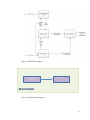
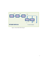
2.1 Block Diagrams
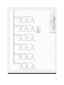
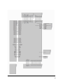
Figure 1: Top Level Block diagram
4"
"
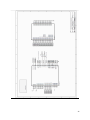
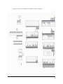
Figure 2: OBD II Block diagram
"
"
Basys2"Development"
Board"
"
FPGA"Board"
"
"
BOOTLOADER)
"
Figure 3: Bootloader Block diagram
5"
"
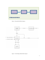
"
"
"
"
"
FPGA"or"MCU"
"
Storage"Media"
(SD"Card)"
"
"
"
ALFAT"SD"
"
Card"Writer""
"
STORAGE)MODULE)
Figure 4: Storage Module Block diagram
Figure 5: Video Display Module Block diagram
6"
"
"
"
"
"
12V"
CAR"
5V"
DC/DC"
Converter"
"
"
"
"
DC/DC"
Converter"
"
"
1.5V"
"
"
"
3.3V"
"
DC/DC"
Converter"
POWER)MODULE) )
)
)
)
)
DC/DC"
Converter"
1.8V"
To"other"modules)
Figure 6: Power Module Block diagram
7"
"
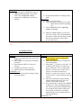
You have described each module and what it does, but you have not described the inputs and outputs of each
model. In other words, you have not described how each module interfaces with the others. For example, you
can write: "The power supply module receives an input from a user controlled switch and outputs a 5V DC
supply voltage for the rest of the blocks. The power supply module contains a converter…."
2.2 Block Descriptions
2.2.1 Overall Summary:
1) Input Data Module: This module obtains input data such as information from the
OBD II and the video images from the camera. The module then converts them into
digital form using an ADC and transmits this digital data to the FPGA.
a. Analog Video: The analog video obtained from the camera on the
windshield. The image will be sent to the ADC to be converted into digital
form.
b. ADC: The Analog-to-Digital converter that converts standard definition
analog video input into a digital form so it can be used by the FPGA. ADC
input is analog video, which is converted to digital images and are then
routed to the FPGA.
c. OBD II: The On-Board Diagnostic system on a car is where information
such as the MIL (malfunction indicator light), DTC (diagnostic trouble
code), I/M (inspection and maintenance) info, etc. can be extracted from. We
will focus on polling operating data like engine RPM, temperature, etc. The
information obtained from this block is sent to the FPGA.
2) FPGA and Control Module: This module is the “brain” of the entire circuit. It
receives the OBD II data and video images from the input module, processes them,
overlays the data onto the video stream. It then routes the overlaid video to the
storage and display modules. This entity also manages video stream
compression/decompression. This block also boots the system.
a. Boot loader: The boot loader is a nonvolatile memory circuit and coprocessor that configures the FPGA for use when system is powered on.
b. JPEG2000 Decoder/Encoder: A device that compresses/decompresses
digital video for extended storage and computer access. This block receives
processed video and data from the FPGA and routes decompressed output
back to the FPGA so that video can be routed to other entities.
c. FPGA: The integrated circuit that will be used to design the digital system to
process the images and data obtained from the OBD II. This block obtains
video from the camera and data from the OBD II, process them, and routes
signal through a video compressor/decompressor. FPGA also streams
processed to a storage device (the MMC) and controls data display for the
attached TFT screen.
3) Storage Module: This module receives the overlaid video from the FPGA and
control module and stores it on a storage device for later use. A compact flash MMC
may be used as the storage device. User can also replay video from the storage
medium.
a. SDHC Flash Memory Card: The flash memory data storage device where
the video and data obtained will be stored. This block obtains the processed
video and data from the FPGA.
b. USB: It is possible to achieve higher storage speeds with an FUSB PHY chip
over USB interface. This item may be used depending on time remaining for
project completion.
4) Display Module: This module displays the overlaid video on a LCD screen from
storage through the FPGA/control block.
a. TFT Display: The LCD display where the processed video obtained from
the FPGA will be displayed.
5) Power Module: This module supplies power to the FPGA and Control Module.
8"
"
2.2.2 Input Module
OBD II Interface:
Register Control
Description: This entity consists of a state machine that performs a loop that first initializes the
ELM327 chip and then loops through a series of states that send and then received data from the
ELM327. The states go from transmitting data, to receiving data, then back to sending, etc. First,
an enable is sent to one of the instruction registers to allow a certain instruction to be sent to the
OBDII. Then, once a signal is received from the register indicating that the data has been sent, the
data register is enabled so as to receive the requested information from the OBDII. Once this data
is received, a signal from the register is made high and sent to the register control, indicating that
the data was received properly. Then the control moves to the next instruction and enables the
appropriate register, but also sends a signal to the converter bank and the video interface
indicating what the last received information was, and enabling the correct conversion entity
depending on that data. Note that only one register enable and one converter enable are ever high
at any given time to ensure that only one instruction is sent or received at a time and that only one
parameter is being converted at a time to ensure that no data gets garbled and to ensure that all the
data is sent and received in a clear order.
Instruction Register Bank
Description: When a register is first initialized, a 4 or 6 byte data signal is set, depending on the
instruction being sent. If the enable is active, then the most significant bit of the data signal is
outputted. Then, the signal is shifted to the left by one bit, and a counter increases by one. This
continues until the counter reaches the number of bits in the instruction. Then, the signal going to
the control register becomes active, indicating that the message has been sent. This causes the
state in the control register to change, causing the enable to go low and the register to reinitialize
to its original value.
Instructions we plan to use:
x0105: Engine coolant temperature
x010A: Fuel pressure
x010C: Engine RPM
x010D: Vehicle speed
x010F: Intake air temperature
x0111: Throttle position
x0146: Ambient air temperature
x015C: Engine oil temperature
Note: These may be changed depending on parameters available for the car we test. The one we
use may not be compatible with some of the instructions listed.
Data Register
Description: When enabled, this register receives data from the OBDII one bit at a time. When a
bit is received, the register shifts the bits to “make room” for the next one. Also, a counter is used
to keep track of the amount of data received. Once all of the data is received, a signal is sent to
the register control to indicate such. Notice that the counter counts to different values depending
on whether one or two bytes are being received.
Converter Bank
9"
"
Description: When enabled, the converter uses an arithmetic equation to change the data received
into the actual, factual information from the engine. The equations used are explained in the
calculations section. These new values are then sent to the video interface. Note that if the
converter is not enabled, its output is set to high impedance, so that only one output is being
transmitted at any time.
2.2.3 FPGA and Control Module
a. Boot loader
According to the Cyclone II Device Handbook, Cyclone II devices use SRAM cells to store
configuration data. Because SRAM memory is volatile, all configuration data will be lost once
the device powers off. Therefore, there’s a need to implement a boot loader to download
configuration data to the Cyclone II devices every time the device powers up.
In our design, we’ll use the Digilent Basys2 development board as the FPGA’s boot loader.
The Cyclone II (or the EP2C35 processor) supports 3 configuration schemes: AS (active serial),
PS (passive serial) and JTAG-based configuration. To select a configuration scheme, the MSEL [
] must be connected to the appropriate digital logic.
Figure 7: Cyclone II Configuration Schemes (Cyclone II Device Handbook, Volume 1, p. 356)"
For our design, the AS scheme will be used, since it has the ability to configure the device at a
high frequency (40MHz).
10"
"
Figure 8: Single Device AS Configuration (Cyclone II Device Handbook, Volume 1, p. 362)"
The EP2C35 essentially goes through 3 states (RESET, CONFIGURATION and
INITIALIZATION) before USER MODE, as depicted below,
RESET"
CONFIGURATION"
INITIALIZATION"
USER"MODE"
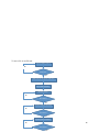
Figure 9: Cyclone II device configuration states
11"
"
"
"
The EP2C35configuration flowchart is as follows,
"
Device"(EP2C35)"in"neutral"
PowerZon"reset"
No"
Successful?"
Yes"
Enter"configuration"mode"
Choose"configuration"scheme"(AS)"
FPGA"enables"config"device"(Basys2)"
No"
Successful?"
Yes"
FPGA"sends"command"and"address"signals"to"Basys2"
"
12"
No"
Successful?"
2.2.4 Storage Module
After the video is processed with the overlaid data, it will be stored on a storage device. We’ll
choose the Transcend 16 GB SDHC Class 10 Flash Memory Card as our storage device. To
simplify the process of writing the file to disk (which involves writing complex memory card and
USB drivers and manipulate buggy file system), we’ll use the ALFAT OEM Board – FAT32 SD
card writer from GHI Electronics.
Figure 10: ALFAT OEM Board (ALFAT SoC Processor User Manual, p. 45)"
The ALFAT SoC processor gives the FPGA a simple way to access storage medias such as SD
cards and USB Mass Storage devices in a very short time. Its key features are as follows:
•
•
LFN (Long File Name) supports.
FAT16 and FAT32 systems.
13"
"
•
•
•
Friendly user-interface through UART, SPI, I2C.
No limits on media size, file size, or file/folder count.
Up to 8 simultaneous file access.
For our design, we choose to implement it using the UART interface. A simple schematic of how
the ALFAT SoC
interacts with
other devices is
as follows,
Figure 11: ALFAT SoC interface (ALFAT SoC Processor User Manual, p. 5)"
After power-up, the Host MCU (our FPGA board) controls the ALFAT SoC by sending in
commands in human-readable ASCII format. The command list is as follows,
Figure 12: ALFAT Command Set (ALFAT SoC Processor User Manual, p. 19)"
14"
"
The command will be send via a UART interface, which uses 3 hardware signals,
•
•
•
UART_TX signal to send data out from ALFAT
UART_RX signal to receive data to ALFAT
UART_BUSY signal which should be monitored while sending data to ALFAT. When
hi, no more data should be transmitted to ALFAT until it gets lo.
Besides, commands are terminated with line-feed, and the user must read back the responses for
each command properly and check whether the command was successful.
To write a file to a storage device, we need the following commands:
•
•
•
I – Initialize and mount the storage device. If this command is not called first, the file
system can be corrupted, and other file related commands will fail.
O – Open file for Read, Write and Append, and give write privileges to it. If the file
already existed, it will be erased and rewritten.
W – Write to file through a file handle assigned to an open file with write mode. This
command is accomplished through 3 steps:
1) Send W command with file handle and the data size
2) Wait til you get the acknowledge
3) Send the data
To make sure the data is written to a file, the file must be flushed or closed when done or
there will be a risk of losing data or corrupting the file system if the storage media was
removed or if there was a power loss.
•
•
F – Flush the data of an opened file. This command is useful to make sure all the data are
physically saved in the media.
C – Close file. This command issues a flush internally and then release the file handle.
The flowchart for a WRITE operation is as follows,
15"
"
To store a file on an SD card:
"
Device"(ALFAT)"neutral"
No"
"
Power"on?"
Yes"
Hold"reset"pins"lo"=>go"to"reset"state"
Select"UART"interface"
Set"reset"pins"hi"
No"
Wait"50ms?"
Yes"
Send"I"(initialize)"command"
No"
Successful?"
Yes"
Send"O"(open)"command"
"
16"
No"
Successful?"
Yes"
2.2.5 Display Module (Software)
Video is inputted into the module from the ADC chip as luma and chroma data, which is stored in
a register. This data is then converted to the RGB color space and is sent to the VGA Controller.
The data from the OBDII module is also sent to the VGA Controller, which uses a ROM to call
upon and display the correct character sprites. Both the raw RGB video data and that of the video
with overlaid data are outputted.
YCrCb Register Bank
Description: 1 byte is sent from the ADC at one time, but the information changes between the
luma value and the chroma value, which is two bytes. There are 3 registers then to hold the last
value sent for each of those. There is also a counter that controls the enable for each register,
which is timed by the input clock. Each of these registers then outputs that byte to the YCrCb to
RGB converter.
17"
"
"
Figure 13: BT.656 8-bit parallel interface data format for 525/60 video systems ( from
AN9728 Application Notes)
YCrCb to RGB Converter
Description: the Y, Cr, and Cb values are all constantly inputted. Then, they are converted into
the RGB color space. The conversion calculations are explained in the next section. Once the
conversions have been performed, the RGB values are sent to the VGA Controller as 3 separate
bytes.
VGA Controller
Description: The VGA Controller will output information for each individual pixel going from
left to right, then up to down. It will output the input for most of these pixels. However, at some
points this entity will call upon the Sprite ROM, which then sends back 8 data bytes, each
corresponding to 8 pixels on a single row of pixels. For each pixel, if the bit from the Sprite ROM
is low, then the video outputted will simply be the RGB value inputted. However, if the value
from the ROM is high, then the pixel will be changed to a different color. This will create
characters on the screen. Some of these will be constant to describe the parameters, such as RPM,
air temperature, etc. Others will be determined by the integer values of the data sent from the
OBDII. These will be the numeric characters, and an if/then statement will be used to display the
appropriate character.
Sprite ROM
Description: This entity acts as a simple read-only ROM, which outputs prewritten data to the
VGA, depending on the address requested. One address is read from at a time, and one address is
outputted at one time. Each address and each line of data are both 1 byte each.
18"
"
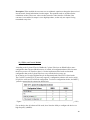
2.2.6 Power Module
The Automotive Racing Video Data Logger device gets power from the 12V car battery.
However, 12V is higher than needed for our device, so DC/DC voltage converters will be
included in the power module to step down 12V to other useful voltages.
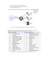
Specifically, here are the power requirements for all the components from the device:
Devices
Digilent Basys2 Development Board
ALFAT OEM Board
FPGA board
TFT LCD display
Voltage(s) needed
3.5V-5.5V
3.3V
3.3V, 1.8V, 1.5V, 1.2V
5V
From the 12V car battery, the voltage will be stepped down to 5V, and then 5V will be stepped
down one more time to get 3.3V to supply power to the ALFAT OEM Board, the FPGA Board,
etc.
3.3V will then be stepped down again to 1.8V and 1.5V to supply power to logic signals on the
FPGA board. The power module block diagram from section 2.1 is copied below to illustrate
how the car power supply will be converted to use on the device:
"
"
"
"
12V"
CAR"
5V"
DC/DC"
Converter"
"
"
"
"
DC/DC"
Converter"
"
"
1.5V"
"
"
"
3.3V"
"
DC/DC"
Converter"
POWER)MODULE) )
)
)
)
)
DC/DC"
Converter"
1.8V"
To"other"modules)
Figure 14: Power Module Block diagram
19"
"
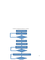
Overall the digital flowchart of the system is as follows,
Initialize"ELM327"
Has data for a
particular
parameter been
received from the
ELM327?"
No"
Yes"
Place"data"in"appropriate"
register"
No"
Is"video"being"
received"from"
our"
camcorder?"
Yes"
Compress"video"
Convert"video"to"RGB"
Send"video"to"
storage"unit"(flash)"
Convert"the"data"into"the"
appropriate"decimal"values"
Organize"information"into"
a"text"or"excel"file"
Send"that"file"to"the"
storage"device"
Interlay"found"values"onto"
the"screen"with"the"original"
video"in"the"background"
Compress"video"
Request"the"next"
parameter"from"the"
ELM327"
Send"video"to"the"
storage"device"
20"
"
Figure 15: of
Overall
Digital
Flowchart
2.3 Schematic
Overall
System
21"
"
Your figures and diagrams need to be numbered and labeled with a description. As they are now, it is unclear to the reader exactly
what is inside each figure.
22"
"
23"
"
24"
"
25"
"
26"
"
27"
"
28"
"
29"
"
30"
"
31"
"
32"
"
33"
"
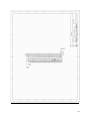
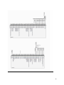
Figure 29: Top Level Schematic of Switches – RS232 – Display
34"
"
35"
"
36"
"
37"
"
38"
"
39"
"
40"
"
2.4 Simulations and Calculations
Color Conversion Calculations:
From Poynton's "Introduction to Digital Video" (p. 176, equations 9.6 and 9.7), the formula to
convert RGB to YCbCr signal is,
YCbCr = T ∗ RGB + offset
where,
65.481
T = −37.797
112
128.553
−74.203
−93.786
24.966
112
−18.214
and,
16
offset = ! 128
128
This equation can be rewritten as,
RGB = ! T !! ∗ (YCbCr − offset)
where,
0.00456621
T !! = ! 0.00456621
0.00456621
0
−0.00153632
0.00791071
0.00625893
−0.00318811
0
Color Conversion Simulation:
Using the derived equations, we implement our color conversion on MATLAB as follows,
41"
"
function [ R, G, B , rgb] = YCbCr2RGB( Y, Cb, Cr )
%Function to convert from YCbCr to RGB used for simulation
% Input checks
if (Y>255 || Y<0 || Cb>255 || Cb<0 || Cr>255 || Cr<0)
error('Invalid Input Range');
end
% Converting to fixed point
max = 255;
Y_r = (Y/max)*(2^7);
Cb_r = (Cb/max)*(2^7);
Cr_r = (Cr/max)*(2^7);
% New fixed point inputs
YCbCr = [Y_r; Cb_r; Cr_r];
% T matrix and offset used for calculations
T = [65.481 128.553 24.966; -37.797 -74.203 112; 112 -93.786
-18.214];
offset = [16;128;128];
% Inverting the T matrix
Tinv = T^-1;
% The final RGB map result
rgb = Tinv*(YCbCr-offset);
%
R
G
B
Converting the fixed point to RGB results
= (rgb(1)/(2^7))*max;
= (rgb(2)/(2^7))*max;
= (rgb(3)/(2^7))*max;
Some results from this MATLAB code are as follows,
42"
"
43"
"
Data Rate:
Our data capture rate is limited by our storage rates. Maximum write speed for the storage
module, ALFAT SoC is only 1400 Kbytes/s, so there will be a need for storage device speed-up
and video capture down-sampling. The FUSB2805 transceiver can be soldered into the ALFAT
SoC to increase the data rate transfer speed. On a FUSB2805, data can be transmitted and receive
at high speed (480Mbps), full speed (12Mbps) and low speed (1.5Mbps) through a 12-bit (SDR)
interface. In other words, 12Mbps is an achievable speed and data rate design calculations use
this rate as a bench mark."
In this project, we use the MAX9526 as our ADC to convert Analog Video into digital signal.
The MAX9526 is a 10-bit 4x oversampling (54Msps) ADC with true 10-but digital processing.
To decrease bandwidth because of storage limitations, however, we will down-sample the video
signals twelve times. We down-sample by 4 to achieve a video rate of 30 fps. After that, we
further down-sample by 3 to achieve 10 fps. In other words, we will sample at a rate of,"
54!Msps
= 4.5!Msps
12
The FPGA gets the digital video signal from at this rate from the MAX9526 ADC, processes it,
overlays it with the data obtained from the OBDII, and sends it to the ADV212 encoder. The
ADV212 has the following data input rates:
Figure 37: Maximum Pixel Data Input Rates for 121-Ball Package (ADV212 Datasheet, p. 32)"
"
44"
"
According to the table, for a VDATA irreversible 10-bit data, with an input of 48 Msps, it is
guaranteed to have the output rate in the range of [98, 150] Mbps.
With our input coming in at a rate of 4.5Msps, the ratio of the actual input rate to the input rate
limit is,
4.5
= 0.09375
48
This gives us a new range of output rate of,
98, 150 Mbps ∗ 0.09375 = 9.2, 14 !Mbps
OBDII Parameters:
The OBDII sends one or two bytes of information which then need additional calculations to
determine the correct values of the parameters. These are done with the following equations,
where A denotes the first byte of data and B denotes the second, if there is a second data byte.
Temperature:
Data = A – 40 (degrees C)
Fuel Pressure:
Data = A * 3 (kPa)
Engine RPM:
Data = ((A * 256) + B) / 4 (rpm)
Vehicle Speed:
Data = A (km/hr)
Throttle Position:
Data = (A * 100) / 255 (%)
45"
"
You have five modules in your block diagram but only 3 modules in the requirements and verification section. There should be a 1-to-1
mapping between each module in your block diagram and a requirement/verification plan.
III.
Requirements and Verification
3.1 Requirements
3.1.1 Requirements Summary:
1) Input Module: This module should successfully obtain the captured video from the
camera and convert it into digital form using an ADC. Besides, this module also
sends the OBD II data to the FPGA and control module without errors.
2) Storage Module: This module should successfully store the overlaid video without
corrupting the file system at a reasonable frame rate.
3) Power Module: This module should supply enough steady power to the circuit.
3.1.2 Verifications Summary
1) Input Module: The video input can be tested simply by displaying the image from
the camcorder onto a screen. The latest OBD II information will be stored in a
register, so we can display the contents of the register onto the screen to be sure they
are correct. If possible we will use an OBD II simulator to verify our measurements.
The signal inputs and outputs will be verified with a logic analyzer to ensure
accuracy.
2) Display Module: We will verify that the real-time video is displayed on our screen.
3) Power Module: We will do a simple check to see if the power supply supplies the
expected voltage and that the circuit stays powered on during an extended period of
time.
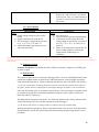
Your verifications lack detail. You need to explain exactly how you will test the requirement. How will you power the device during
testing? What equipment will you use to probe the output? What is a "proper" output? What should the inputs to the module be?
How will you supply these inputs?
3.1.3 Input Module
Requirements
Camcorder:
1) Output video signal is analog SD NTSC-M
signal
MAX9526:
2) Output video is ITU-R.656 uncompressed
digital video
3) Ensure that the ADC chip is powered at the
correct wattage
4) Configure the MAX9526 correctly
Verifications
Camcorder:
1) Ensure analog source, the camcorder, is
powered on and output is enabled by:
a) Power the camera and check that it
outputs a proper signal
MAX9526:
2) Check ADC chip power.
3) Check that the ADC is programmed
This needs more detail. How will you power the camera? How will you check its output? What is a proper output?
"
46"
WIG-09555:
5) Input data signal is OBDII data from car
6) OBDII to ELM signaling is set to ISO
9141-2 for Asian make vehicles
7) Output data is OBDII info over RS-232
interface
properly.
4) Program the MAX9536 according to data
sheet.
WIG-09555:
5) Ensure car is powered on:
6) Check automotive accessory power outlet:
a. Check that the outlet is outputting
12 V
7) Verify OBDII ISO 9141-2 signaling
scheme is selected.
6) Make sure OBDII module is powered on
and is set correctly. Store sent information
in a register, and use the hex display on the
FPGA to check that the correct data is
received and stored
How will you check the ADC power? Using a multimeter? Oscilloscope? What inputs must the ADC be supplied
with?
3.1.6 Display Module
Requirements
ADV212:
1) Displays decompressed video equivalent to
capture rate
2) Video output size maximum of 800X480
resolution
3) Ensure that the ADV212 is powered
correctly
4) Configure the ADV212 correctly
5) ADV212 must be initiated properly
K50DWN0-V1-F:
6) Ensure the correct power wattage is being
sent to the display
"
Verifications
ADV212:
1) Ensure interface clock is configured to
proper clocking rate
2) Ensure JPEG2000 video is decompressed
and scaled properly
3) Check that VDD is between 1.425 and 1.575
V and that IDD is between 55 and 65 mA
using a multimeter. Also, we must check
that VDDIO is between 3.135 and 3.465 V
and IDDIO is between 40 and 50 mA.
Finally, VIN needs to be between -0.3 and
3.765 V and IDYN must be between 280 and
320 mA.
4) This can be checked by communicating
with the chip through a CPU via a free
software codec such as Kakadu.
5) First, 0x400 must be written to the EIRQIE
at address 0x5. Then, the IRQ pin will go
low, and we will check that EIRQFLG[10]
is set using the FPGA and a simple code.
We will also use the FPGA to read the
application ID to ensure that the chip was
correctly initialized.
K50DWN0-V1-F
What is the proper clocking rate for the display? How will you check the clocking rate? What equipment will
you need?
47"
6) Use a multimeter to ensure that VCC is
between -0.3 and 5.0V and ICC is between
25 and 35 mA. Also, VDD must be between
3.0 and 3.6 V and IDD has to be between 15
and 19 mA.
3.1.7 Power Module
Requirements
Power:
1) Supply enough voltage to power on the
board
2) Supply constant power to the board
3) The car voltage is stepped down correctly
to 5V, 3.3V, 1.8V, 1.2V and 1.5V
4) All the individual components power on
and work consistently
Verifications
Power:
1) Car outlet is live
2) The board doesn’t power off intermittently
3) A multimeter will be used to check the
voltage output of each DC/DC converter to
see if 5V, 3.3V, 1.8V, 1.2V and 1.5V are
achieved
4) Ensure each component is connected to its
correct voltage supply by checking the
voltage before connecting it to a
component.
The tolerance analysis is incomplete. You have described what tolerance range is acceptable for the ADC oscillator but you have not
explained why the ADC oscillator is vital to your project. Moreover, you have not described how you will verify that this range of tolerances
is acceptable.
3.2 Tolerance Analysis
Oscillator Frequencies: Verify that the ADC oscillator crystal has a frequency of 27 MHz, plus
or minus 50 ppm.
3.3 Ethical Issues
The purpose of this project is to develop a data logger device for racer, which helps them to better
manage the condition of the car while racing. With such function, our device helps increase the
safety and health of the driver, which is consistent with the first code of the IEEE Code of Ethics:
1. to accept responsibility in making decisions consistent with the safety, health, and welfare of
the public, and to disclose promptly factors that might endanger the public or the environment;
One of the factors that cause car accidents is system defects. Our device helps prevent these kinds
of accidents by giving drivers immediate information about the system s other car while also
them with video of a driving car.
Throughout the development of the device, we will follow the third code closely, and only make
claims and estimates based on real data acquired from our data logger.
3. to be honest and realistic in stating claims or estimates based on available data;
Working with a data logger device, the most importance factor is the accuracy of the information
obtained from the system. We will be honest and will not falsify the data acquired from our test
procedures.
48"
"
After this project, we will have learned a great deal about various real-world industrial systems
such as the On-board Diagnostic (OBD II) system, the SD Flash memory FAT 32 file system, or
the ITU-R BT 656 protocol. This will improve our understanding of these technologies and their
applications, and also improve our technical competence, as directed in the 5th and 6th codes of the
IEEE Code of Ethics:
5. to improve the understanding of technology; its appropriate application, and potential
consequences;
6. to maintain and improve our technical competence and to undertake technological tasks for
others only if qualified by training or experience, or after full disclosure of pertinent limitations;
Furthermore, while working on the project, we will build an environment that promote engineer
professionalism, which welcomes constructive and honest criticisms, acknowledges errors, assists
peer workers with their professional and academic developments, and credits appropriate
contributions, as cited in the 7th and 10th codes of the IEEE Code of Ethics:
7. to seek, accept, and offer honest criticism of technical work, to acknowledge and correct
errors, and to credit properly the contributions of others;
10. to assist colleagues and co-workers in their professional development and to support them in
following this code of ethics.
Following the 9th code of the IEEE Code of Ethics,
9. to avoid injuring others, their property, reputation, or employment by false or malicious
action;
We will make sure that the data logger device developed from this project will offer the users
with data that is as accurate as possible, and will not provide them with false information, in order
to avoid damaging that could occur to the users’ health, their car or other properties.
IV.
Cost and Schedule
4.1 Cost Analysis
a. Labor
Name
Tung Do
Nick Greenway
Andrew Wesly
Total
b. Parts
Description
Encoder/Decoder
Development Board
Interperter
Decoder
Converter
Rate
$50/hr
$50/hr
$50/hr
Hours
180
180
180
Total
$9000
$9000
$9000
#
Manufacturer
Vendor
1
1
1
1
1
Analog Devices
Altera DE2
Elm Electronics
Maxim Integrated
Sparkfun
Digikey
NA
ELM Electronics
Mouser
Total x 2.5
$22500
$22500
$22500
$67500
Cost/uni
t
$48.984
$269
$23.50
$7.97
$49.95
Total
Cost
$48.984
0 - Have
$23.50
$7.97
$49.95
49"
"
You need to have part numbers in your bill of materials.
Control Switches
FPGA
Digilent Basys2
Development Board –
used as bootloader
Card writer
Display
Total Labor Cost
$67,500
6
1
1
Electronics
C&K Compnents
Altera
DigilentInc
Mouser
Altera
DigilentInc
$6.25
$149.50
$100.00
$37.50
$149.50
0 - Have
1
1
GHI Electronics
Kentec
GHI Electronics
Newark
$59.95
$65.22
$59.95
$65.22
Total Parts Cost
$791.59
Total Project Cost
$68,291.59
A task can only have one person in charge of it. Therefore, you cannot have a task which is to be done by "All". Research is
not sufficient for an entire week for one person. Neither is ordering parts. You should not have any "to be decided" weeks.
You need to create a plan for the semester. If this plan changes, that is fine. But at the least you need to set out a course of
action.
4.2 Schedule
Week
9/16
9/23
9/30
Task Description
Proposals Due
Software design for storage and boot loader
Software design for OBD II and ITU-R BT. 656
Research Hardware
Design Reviews Sign-up Closes
Finalize the schematic
Design Reviews
Order storage interface
Test OBD II interface
Board layout/order components
Group
Members
Tung Do
Nick Greenway
Andrew Wesly
All
Tung Do
Nick Greenway
Andrew Wesly
10/7
Software development for Boot loader
Software development for Video interface
Submit board for fab
Tung Do
Nick Greenway
Andrew Wesly
Test boot loader
Test video interface
Assemble the boards
Individual Progress Reports Due
Test overlaid video on storage device
Verify correctness of OBD II data obtained
Test assembled boards
All
Nick Greenway
Andrew Wesly
10/14
10/21
Tung Do
Nick Greenway
Andrew Wesly
10/28
50"
"
11/4
11/11
11/18
11/25
12/2
12/9
TBD
TBD
TBD
Mock-up Demos and Mock Presentation Sign-up closes
Mock Presentation – Control Slides
Mock Presentation – Test Slides
Mock Presentation – Design Slides
Last Day to Request 1st Revision PCB Fabrication
Final software testing
Final software testing
Assemble everything in an enclosure
Thanksgiving Break, Last day to Request Final Revision PCB
fab
Demo and Presentation Sign-up closes
Final tests and verifications
Final tests and verifications
Final tests and verifications
Demos and Presentations
Demo, Final Paper – Intro & Conclusion
Presentation, Final Paper – Testing & Verification
Demo, Final Paper – Design Procedure
Presentations, Checkout, Final Paper, Lab Notebooks
Final Paper & Notebook review and hand-in
Final Paper & Notebook review and hand-in
Final Paper & Notebook review and hand-in
Tung Do
Nick Greenway
Andrew Wesly
Tung Do
Nick Greenway
Andrew Wesly
Tung Do
Nick Greenway
Andrew Wesly
Tung Do
Nick Greenway
Andrew Wesly
Tung Do
Nick Greenway
Andrew Wesly
Tung Do
Nick Greenway
Andrew Wesly
4.1 Contingency Plan
-
In case of exorbitant pcb costs or a crunch for time the following contingency plan may be
executed to deliver on proposed Automotive Racing Video Data Logger.
-
Replace FPGA IC, MAX9526 ADC IC, RS232 MODULE, and CONTROL switches with
Altera DE2 board.
-
Modify power supply module to supply 9V to development board
-
Connect ALFAT module to board, OBDII module to board
51"
"
-
Create TFT display connections
-
Possibly implement JPEG2000 encoder/decoder.
-
Frame rates may be as low as 1fps
References:
78SR 2 Amp Series, Murata, Mansfield, MA, 2009. [Online]. Available: http://www.murataps.com/data/meters/mpm_78sr-2a_a00.pdf
ADV212, Rev. B, Analog Devices, Norwood, MA, 2010. [Online]. Available:
http://www.analog.com/static/imported-files/data_sheets/ADV212.pdf
ALFAT SoC Processor User Manual, Rev. 1.12, GHI Electronics, Macomb Township, MI, 2012.
[Online]. Available:
http://www.ghielectronics.com/downloads/ALFAT/ALFAT%20SoC%20Processor%20User%20Manual.
pdf
BT.656 Video Interface for ICs, Intersil, Milpitas, CA, 2002. [Online]. Available:
http://www.intersil.com/content/dam/Intersil/documents/an97/an9728.pdf
Charles A. Poynton, A Technical Introduction to Digital Video,
John Wiley & Sons, Inc., 1996, p. 175-176
Cyclone II Device Handbook, Volume 1, Altera, San Jose, CA, 2008. [Online]. Available:
http://www.altera.com/literature/hb/cyc2/cyc2_cii5v1.pdf
Cyclone II EP2C35 PCI Development Board Reference Manual, Version 1, Altera, San Jose, CA, 2005.
[Online]. Available: http://www.altera.com/literature/manual/rm_pci_dev_bd_cyclone2_ed.pdf
Digilent Basys 2Board Reference Manual, Digilent, Pullman, WA, 2010. [Online]. Available:
https://www.digilentinc.com/Data/Products/BASYS2/Basys2_rm.pdf
ELM327, ELM, Toronto, [Online]. Available: http://elmelectronics.com/DSheets/ELM327DS.pdf
FS-K50DWN0-V1-F, Rev. 2, Kentec Display, 2011. [Online]. Available:
http://www.kentecdisplay.com/uploads/soft/Products_spec/K50DWN0-V1-F-01_KED_.pdf
52"
"
IEEE Code of Ethics [Online]. Available: http://www.ieee.org/about/corporate/governance/p7-8.html
MAX9526, Rev. 3, Maxim Integrated, San Jose, CA, [Online]. Available:
http://datasheets.maximintegrated.com/en/ds/MAX9526.pdf
MPDTY Series, Murata, Mansfield, MA, [Online]. Available:
http://search.murata.co.jp/Ceramy/image/img/A14X/M07E1.pdf
NDTS Series, Murata, Mansfield, MA, 2012 [Online]. Available: http://www.murataps.com/data/power/ncl/kdc_ndts.pdf
OBD-II UART [Online]. Available: https://www.sparkfun.com/products/9555
Recommendation ITU-R BT.601-5: Studio Encoding Parameters of Digital Television for Standard 4:3 and
Widescreen 16:9 Aspect Ratios, 1995. [Online]. Available:
http://www.intersil.com/content/dam/Intersil/documents/an97/an9728.pdf
Single Output LSN-10A Models, Murata, Mansfield, MA, 2009. [Online]. Available: http://www.murataps.com/data/power/lsn10a-d5.pdf
Single Output LSN-W3 Models, Murata, Mansfield, MA, 2009. [Online]. Available: http://www.murataps.com/data/power/lsn16a-w3.pdf
53"
"