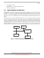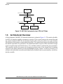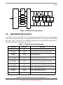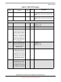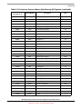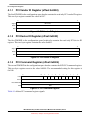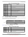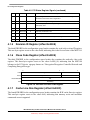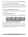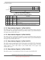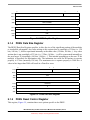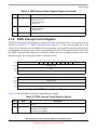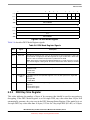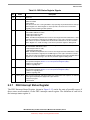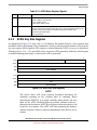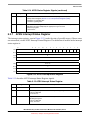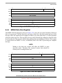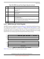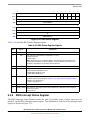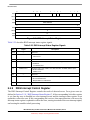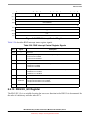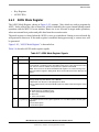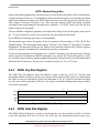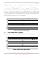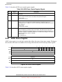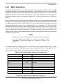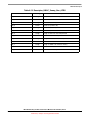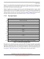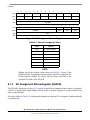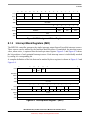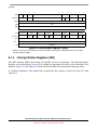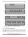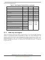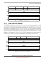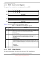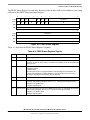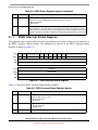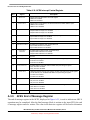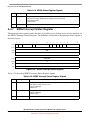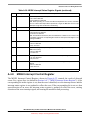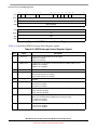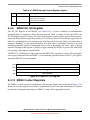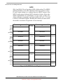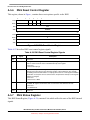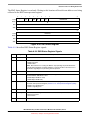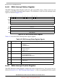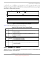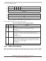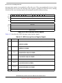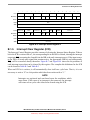
1
MPC184 Security Co-Processor
User’s Manual
PCI Interface
MPC184UM
Rev. 2, 12/2005
Preliminary—Subject to Change Without Notice
How to Reach Us:
Home Page:
www.freescale.com
email:
[email protected]
USA/Europe or Locations Not Listed:
Freescale Semiconductor
Technical Information Center, CH370
1300 N. Alma School Road
Chandler, Arizona 85224
(800) 521-6274
480-768-2130
[email protected]
Europe, Middle East, and Africa:
Freescale Halbleiter Deutschland GmbH
Technical Information Center
Schatzbogen 7
81829 Muenchen, Germany
+44 1296 380 456 (English)
+46 8 52200080 (English)
+49 89 92103 559 (German)
+33 1 69 35 48 48 (French)
[email protected]
Japan:
Freescale Semiconductor Japan Ltd.
Headquarters
ARCO Tower 15F
1-8-1, Shimo-Meguro, Meguro-ku
Tokyo 153-0064, Japan
0120 191014
+81 3 5437 9125
[email protected]
Information in this document is provided solely to enable system and software
implementers to use Freescale Semiconductor products. There are no express or
implied copyright licenses granted hereunder to design or fabricate any integrated
circuits or integrated circuits based on the information in this document.
Freescale Semiconductor reserves the right to make changes without further notice to
any products herein. Freescale Semiconductor makes no warranty, representation or
guarantee regarding the suitability of its products for any particular purpose, nor does
Freescale Semiconductor assume any liability arising out of the application or use of
any product or circuit, and specifically disclaims any and all liability, including without
limitation consequential or incidental damages. “Typical” parameters which may be
provided in Freescale Semiconductor data sheets and/or specifications can and do
Asia/Pacific:
Freescale Semiconductor Hong Kong Ltd.
Technical Information Center
2 Dai King Street
Tai Po Industrial Estate,
Tai Po, N.T., Hong Kong
+800 2666 8080
[email protected]
vary in different applications and actual performance may vary over time. All operating
For Literature Requests Only:
Freescale Semiconductor
Literature Distribution Center
P.O. Box 5405
Denver, Colorado 80217
(800) 441-2447
303-675-2140
Fax: 303-675-2150
LDCForFreescaleSemiconductor
@hibbertgroup.com
could create a situation where personal injury or death may occur. Should Buyer
parameters, including “Typicals” must be validated for each customer application by
customer’s technical experts. Freescale Semiconductor does not convey any license
under its patent rights nor the rights of others. Freescale Semiconductor products are
not designed, intended, or authorized for use as components in systems intended for
surgical implant into the body, or other applications intended to support or sustain life,
or for any other application in which the failure of the Freescale Semiconductor product
purchase or use Freescale Semiconductor products for any such unintended or
unauthorized application, Buyer shall indemnify and hold Freescale Semiconductor
and its officers, employees, subsidiaries, affiliates, and distributors harmless against all
claims, costs, damages, and expenses, and reasonable attorney fees arising out of,
directly or indirectly, any claim of personal injury or death associated with such
unintended or unauthorized use, even if such claim alleges that Freescale
Semiconductor was negligent regarding the design or manufacture of the part.
Freescale™ and the Freescale logo are trademarks of Freescale Semiconductor, Inc. All other
product or service names are the property of their respective owners.
© Freescale Semiconductor, Inc., 2005. All rights reserved.
Document Number: MPC184UM
Rev. 2, 12/2005
Preliminary—Subject to Change Without Notice
Overview
1
Signal Descriptions
2
Address Map
3
PCI Configuration Registers
4
Execution Units
5
MPC184 Descriptors
6
Crypto-Channels
7
Controller
8
PCI Interface Module
9
Execution Units in 32-Bit Big Endian View
A
Controller in 32-Bit Big Endian View
B
User’s Manual Revision History
C
Index
Preliminary—Subject to Change Without Notice
IND
1
Overview
2
Signal Descriptions
3
Address Map
4
PCI Configuration Registers
5
Execution Units
6
MPC184 Descriptors
7
Crypto-Channels
8
Controller
9
PCI Interface Module
A
Execution Units in 32-Bit Big Endian View
B
Controller in 32-Bit Big Endian View
C
User’s Manual Revision History
IND
Index
Preliminary—Subject to Change Without Notice
Contents
Paragraph
Number
Title
Page
Number
Chapter 1
Overview
1.1
1.2
1.3
1.4
1.5
1.6
1.6.1
1.6.2
1.6.3
1.6.4
1.6.5
1.6.6
1.7
1.7.1
1.7.1.1
1.7.1.2
1.7.2
1.7.3
1.7.4
1.7.5
1.7.6
1.7.7
1.8
1.9
Development History ....................................................................................................... 1-1
Typical Applications ........................................................................................................ 1-1
Features ............................................................................................................................ 1-1
Typical System Architecture............................................................................................ 1-3
Architectural Overview.................................................................................................... 1-4
Data Packet Descriptors................................................................................................... 1-5
External Bus Interface ................................................................................................. 1-6
The MPC184 Controller .............................................................................................. 1-7
Host-Managed Register Access ................................................................................... 1-7
Static EU Access.......................................................................................................... 1-7
Dynamic EU Access .................................................................................................... 1-7
Crypto-Channels .......................................................................................................... 1-8
Execution Units (EUs) ..................................................................................................... 1-8
Public Key Execution Unit (PKEU) ............................................................................ 1-9
Elliptic Curve Operations ........................................................................................ 1-9
Modular Exponentiation Operations...................................................................... 1-10
Data Encryption Standard Execution Unit (DEU)..................................................... 1-10
Arc Four Execution Unit (AFEU) ............................................................................. 1-10
Advanced Encryption Standard Execution Unit (AESU).......................................... 1-11
Message Digest Execution Unit (MDEU) Module.................................................... 1-11
Random Number Generator (RNG)........................................................................... 1-11
8KB General Purpose RAM (gpRAM) ..................................................................... 1-12
Performance Estimates .................................................................................................. 1-12
User’s Manual Revision History.................................................................................... 1-12
Chapter 2
Signal Descriptions
2.1
2.2
Signal Descriptions .......................................................................................................... 2-1
MPC184 Pin Out.............................................................................................................. 2-4
Chapter 3
Address Map
3.1
Address Map .................................................................................................................... 3-1
MPC184 Security Co-Processor User’s Manual: PCI Interface, Rev. 2
Freescale Semiconductor
v
Preliminary—Subject to Change Without Notice
Contents
Paragraph
Number
Title
Page
Number
Chapter 4
PCI Configuration Registers
4.1
4.1.1
4.1.2
4.1.3
4.1.4
4.1.5
4.1.6
4.1.7
4.1.8
4.1.9
4.1.10
4.1.11
4.1.12
4.1.13
4.1.14
4.1.15
4.1.16
4.1.17
4.1.18
4.1.19
4.1.20
4.1.21
4.1.22
4.1.23
4.1.24
4.1.25
PCI Configuration Space ................................................................................................. 4-1
PCI Vendor ID Register (offset 0x0000) ..................................................................... 4-2
PCI Device ID Register (offset 0x0002)...................................................................... 4-2
PCI Command Register (offset 0x0004) ..................................................................... 4-2
PCI Status Register (offset 0x0006) ............................................................................ 4-3
Revision ID Register (offset 0x0008) .......................................................................... 4-4
Class Code Register (offset 0x0009) ........................................................................... 4-4
Cache Line Size Register (offset 0x000C) .................................................................. 4-4
Latency Timer Register (offset 0x000D) ..................................................................... 4-5
Header-Type Register (offset 0x000E) ........................................................................ 4-5
BIST Register (offset 0x000F) .................................................................................... 4-5
Base Address Register Zero (offset 0x0010) ............................................................... 4-5
Base Address Register 1 (offset 0x0014) .................................................................... 4-6
Base Address Register 2 (offset 0x0018) .................................................................... 4-6
Base Address Register 3 (offset 0x001C).................................................................... 4-6
Base Address Register 4 (offset 0x0020) .................................................................... 4-6
Base Address Register 5 (offset 0x0024) .................................................................... 4-7
CardBus CIS Pointer Register (offset 0x0028)............................................................ 4-7
Subsystem Vendor ID Register (offset 0x002C).......................................................... 4-7
Subsystem ID Register (offset 0x002E) ...................................................................... 4-7
Expansion ROM Base Address Register (offset 0x0030) ........................................... 4-8
Capabilities Pointer (offset 0x0034) ............................................................................ 4-8
Interrupt Line Register (offset 0x003C) ...................................................................... 4-8
Interrupt Pin Register (offset 0x003D) ........................................................................ 4-8
Min_GNT Register (offset 0x003D)............................................................................ 4-8
Max_Lat Register (offset 0x003F) .............................................................................. 4-9
Chapter 5
Execution Units
5.1
5.1.1
5.1.2
5.1.3
5.1.4
5.1.5
5.1.6
5.1.7
Public Key Execution Units (PKEU)............................................................................... 5-2
PKEU Register Map .................................................................................................... 5-2
PKEU Mode Register .................................................................................................. 5-2
PKEU Key Size Register ............................................................................................. 5-4
PKEU Data Size Register ............................................................................................ 5-5
PKEU Reset Control Register...................................................................................... 5-5
PKEU Status Register .................................................................................................. 5-6
PKEU Interrupt Status Register ................................................................................... 5-8
MPC184 Security Co-Processor User’s Manual: PCI Interface, Rev. 2
vi
Freescale Semiconductor
Preliminary—Subject to Change Without Notice
Contents
Paragraph
Number
5.1.8
5.1.9
5.1.10
5.1.10.1
5.1.10.2
5.1.10.3
5.1.10.4
5.2
5.2.1
5.2.2
5.2.3
5.2.4
5.2.5
5.2.6
5.2.7
5.2.8
5.2.9
5.2.10
5.2.11
5.2.12
5.3
5.3.1
5.3.2
5.3.2.1
5.3.2.2
5.3.3
5.3.4
5.3.5
5.3.6
5.3.7
5.3.8
5.3.9
5.3.10
5.3.10.1
5.3.10.2
5.3.11
5.3.12
5.4
5.4.1
5.4.2
5.4.2.1
Title
Page
Number
PKEU Interrupt Control Register ................................................................................ 5-9
PKEU EU_GO Register............................................................................................. 5-10
PKEU Parameter Memories....................................................................................... 5-11
PKEU Parameter Memory A ................................................................................. 5-11
PKEU Parameter Memory B ................................................................................. 5-11
PKEU Parameter Memory E ................................................................................. 5-11
PKEU Parameter Memory N ................................................................................. 5-11
Data Encryption Standard Execution Units (DEU) ....................................................... 5-11
DEU Register Map..................................................................................................... 5-12
DEU Mode Register................................................................................................... 5-12
DEU Key Size Register ............................................................................................. 5-13
DEU Data Size Register ............................................................................................ 5-14
DEU Reset Control Register...................................................................................... 5-15
DEU Status Register .................................................................................................. 5-16
DEU Interrupt Status Register ................................................................................... 5-17
DEU Interrupt Control Register................................................................................. 5-19
DEU EU_GO Register............................................................................................... 5-21
DEU IV Register........................................................................................................ 5-22
DEU Key Registers.................................................................................................... 5-22
DEU FIFOs ................................................................................................................ 5-22
ARC Four Execution Unit (AFEU) ............................................................................... 5-22
AFEU Register Map .................................................................................................. 5-22
AFEU Mode Register ................................................................................................ 5-23
Host-provided Context via Prevent Permute ......................................................... 5-23
Dump Context........................................................................................................ 5-23
AFEU Key Size Register ........................................................................................... 5-25
AFEU Context/Data Size Register ............................................................................ 5-26
AFEU Reset Control Register.................................................................................... 5-26
AFEU Status Register ................................................................................................ 5-27
AFEU Interrupt Status Register ................................................................................. 5-29
AFEU Interrupt Control Register .............................................................................. 5-30
AFEU End of Message Register................................................................................ 5-32
AFEU Context ........................................................................................................... 5-32
AFEU Context Memory ........................................................................................ 5-33
AFEU Context Memory Pointer Register.............................................................. 5-33
AFEU Key Registers ................................................................................................. 5-33
AFEU FIFOs.............................................................................................................. 5-33
Message Digest Execution Units (MDEU).................................................................... 5-34
MDEU Register Map ................................................................................................. 5-34
MDEU Mode Register ............................................................................................... 5-34
Recommended settings for MDEU Mode Register ............................................... 5-36
MPC184 Security Co-Processor User’s Manual: PCI Interface, Rev. 2
Freescale Semiconductor
vii
Preliminary—Subject to Change Without Notice
Contents
Paragraph
Number
5.4.3
5.4.4
5.4.5
5.4.6
5.4.7
5.4.8
5.4.9
5.4.10
5.4.11
5.4.12
5.5
5.5.1
5.5.2
5.5.3
5.5.4
5.5.5
5.5.6
5.5.7
5.5.8
5.5.9
5.5.10
5.5.11
5.6
5.6.1
5.6.2
5.6.3
5.6.4
5.6.5
5.6.6
5.6.7
5.6.8
5.6.9
5.6.9.1
5.6.9.2
5.6.9.3
5.6.9.4
5.6.9.5
Title
Page
Number
MDEU Key Size Register.......................................................................................... 5-36
MDEU Data Size Register......................................................................................... 5-37
MDEU Reset Control Register .................................................................................. 5-38
MDEU Status Register............................................................................................... 5-38
MDEU Interrupt Status Register................................................................................ 5-40
MDEU Interrupt Control Register ............................................................................. 5-41
MDEU EU_GO Register ........................................................................................... 5-42
MDEU Context Registers .......................................................................................... 5-43
MDEU Key Registers ................................................................................................ 5-44
MDEU FIFOs ............................................................................................................ 5-45
Random Number Generator (RNG)............................................................................... 5-45
Overview.................................................................................................................... 5-45
Functional Description............................................................................................... 5-45
RNG Register Map .................................................................................................... 5-46
RNG Mode Register .................................................................................................. 5-46
RNG Data Size Register ............................................................................................ 5-47
RNG Reset Control Register...................................................................................... 5-47
RNG Status Register .................................................................................................. 5-48
RNG Interrupt Status Register ................................................................................... 5-49
RNG Interrupt Control Register ................................................................................ 5-50
RNG EU_GO Register............................................................................................... 5-51
RNG FIFO ................................................................................................................. 5-52
Advanced Encryption Standard Execution Units (AESU) ............................................ 5-52
AESU Register Map .................................................................................................. 5-52
AESU Mode Register ................................................................................................ 5-53
AESU Key Size Register ........................................................................................... 5-54
AESU Data Size Register .......................................................................................... 5-54
AESU Reset Control Register.................................................................................... 5-55
AESU Status Register ................................................................................................ 5-56
AESU Interrupt Status Register ................................................................................. 5-57
AESU Interrupt Control Register .............................................................................. 5-59
AESU End of Message Register................................................................................ 5-61
AESU Context Registers ....................................................................................... 5-61
Context for CBC Mode.......................................................................................... 5-62
Context for Counter Mode..................................................................................... 5-63
AESU Key Registers ............................................................................................. 5-63
AESU FIFOs.......................................................................................................... 5-64
Chapter 6 MPC184 Descriptors
6.1
Data Packet Descriptor Overview.................................................................................... 6-1
MPC184 Security Co-Processor User’s Manual: PCI Interface, Rev. 2
viii
Freescale Semiconductor
Preliminary—Subject to Change Without Notice
Contents
Paragraph
Number
6.2
6.2.1
6.2.2
6.3
6.3.1
6.4
6.4.1
6.4.2
Title
Page
Number
Descriptor Structure ......................................................................................................... 6-1
Descriptor Header ........................................................................................................ 6-2
Descriptor Length and Pointer Fields .......................................................................... 6-5
Descriptor Chaining ......................................................................................................... 6-7
Null Fields.................................................................................................................... 6-8
Descriptor Classes............................................................................................................ 6-8
Static Descriptors ......................................................................................................... 6-9
Dynamic Descriptors ................................................................................................. 6-12
Chapter 7
Crypto-Channels
7.1
7.1.1
7.1.2
7.1.3
7.1.4
7.1.5
7.1.5.1
7.1.5.2
7.1.5.3
7.2
7.2.1
7.2.2
7.2.3
7.2.3.1
7.2.3.2
Crypto-Channel Registers................................................................................................ 7-2
Crypto-Channel Configuration Register (CCCR)........................................................ 7-2
Crypto-Channel Pointer Status Registers (CCPSR) .................................................... 7-5
Crypto-Channel Current Descriptor Pointer Register (CDPR).................................. 7-10
Fetch Register (FR).................................................................................................... 7-11
Descriptor Buffer (DB) .............................................................................................. 7-12
Descriptor Header.................................................................................................. 7-13
Descriptor Length/Pointer Pairs ............................................................................ 7-14
Next Descriptor Pointer ......................................................................................... 7-14
Interrupts ........................................................................................................................ 7-14
Channel Done Interrupt ............................................................................................. 7-14
Channel Error Interrupt.............................................................................................. 7-15
Channel Reset ............................................................................................................ 7-15
Hardware Reset...................................................................................................... 7-15
Channel Specific Software Reset........................................................................... 7-15
Chapter 8
Controller
8.1
8.1.1
8.1.2
8.1.3
8.1.4
8.1.5
8.1.6
8.1.7
8.1.8
8.1.9
Controller Registers ......................................................................................................... 8-1
EU Assignment Control Register (EUACR) ............................................................... 8-1
EU Assignment Status Register (EUASR) .................................................................. 8-2
Interrupt Mask Registers (IMR) .................................................................................. 8-3
Interrupt Status Registers (ISR) ................................................................................... 8-4
Interrupt Clear Register (ICR) ..................................................................................... 8-5
ID Register................................................................................................................... 8-8
Master Control Registers (MCR)................................................................................. 8-9
EU Access.................................................................................................................. 8-11
Multiple EU Assignment ........................................................................................... 8-12
MPC184 Security Co-Processor User’s Manual: PCI Interface, Rev. 2
Freescale Semiconductor
ix
Preliminary—Subject to Change Without Notice
Contents
Paragraph
Number
8.1.10
8.1.11
8.1.12
8.1.13
Title
Page
Number
Multiple Channels...................................................................................................... 8-12
Priority Arbitration .................................................................................................... 8-12
Round Robin Snapshot Arbiters ................................................................................ 8-13
Bus Access................................................................................................................. 8-13
Chapter 9
PCI Interface Module
9.1
9.2
9.2.1
9.2.2
9.2.3
9.2.4
9.2.5
9.2.6
9.2.6.1
9.2.6.2
9.2.7
9.2.8
9.2.9
PCI Interface .................................................................................................................... 9-1
PCI Initiator ..................................................................................................................... 9-1
Data Alignment Block ................................................................................................. 9-1
Bus Access................................................................................................................... 9-1
Bus Arbitration ............................................................................................................ 9-2
PCI Initiator ................................................................................................................. 9-3
Parity Errors................................................................................................................. 9-3
PCI Read ...................................................................................................................... 9-3
Target Aborts ........................................................................................................... 9-4
Initiator Aborts and Retry Errors ............................................................................. 9-4
Initiator Write............................................................................................................... 9-4
Misaligned Data........................................................................................................... 9-5
PCI Target .................................................................................................................... 9-6
Appendix A
Execution Units in 32-Bit Big Endian View
A.1
A.1.1
A.1.2
A.1.3
A.1.4
A.1.5
A.1.6
A.1.7
A.1.8
A.1.9
A.1.10
A.1.10.1
A.1.10.2
A.1.10.3
A.1.10.4
A.2
Public Key Execution Units (PKEU).............................................................................. A-2
PKEU Register Map ................................................................................................... A-2
PKEU Mode Register ................................................................................................. A-2
PKEU Key Size Register ............................................................................................ A-4
PKEU Data Size Register ........................................................................................... A-5
PKEU Reset Control Register..................................................................................... A-6
PKEU Status Register ................................................................................................. A-6
PKEU Interrupt Status Register .................................................................................. A-8
PKEU Interrupt Control Register ............................................................................... A-9
PKEU EU_GO Register.............................................................................................A-11
PKEU Parameter Memories.......................................................................................A-11
PKEU Parameter Memory A .................................................................................A-11
PKEU Parameter Memory B .................................................................................A-11
PKEU Parameter Memory E ................................................................................ A-12
PKEU Parameter Memory N ................................................................................ A-12
Data Encryption Standard Execution Units (DEU) ...................................................... A-12
MPC184 Security Co-Processor User’s Manual: PCI Interface, Rev. 2
x
Freescale Semiconductor
Preliminary—Subject to Change Without Notice
Contents
Paragraph
Number
A.2.1
A.2.2
A.2.3
A.2.4
A.2.5
A.2.6
A.2.7
A.2.8
A.2.9
A.2.10
A.2.11
A.2.12
A.3
A.3.1
A.3.2
A.3.2.1
A.3.2.2
A.3.3
A.3.4
A.3.5
A.3.6
A.3.7
A.3.8
A.3.9
A.3.10
A.3.10.1
A.3.10.2
A.3.11
A.3.12
A.4
A.4.1
A.4.2
A.4.3
A.4.4
A.4.5
A.4.6
A.4.7
A.4.8
A.4.9
A.4.10
A.4.11
Title
Page
Number
DEU Register Map.................................................................................................... A-12
DEU Mode Register.................................................................................................. A-12
DEU Key Size Register ............................................................................................ A-14
DEU Data Size Register ........................................................................................... A-14
DEU Reset Control Register..................................................................................... A-15
DEU Status Register ................................................................................................. A-16
DEU Interrupt Status Register .................................................................................. A-17
DEU Interrupt Control Register................................................................................ A-19
DEU EU_GO Register.............................................................................................. A-21
DEU IV Register....................................................................................................... A-22
DEU Key Registers................................................................................................... A-22
DEU FIFOs ............................................................................................................... A-22
ARC Four Execution Unit (AFEU) .............................................................................. A-22
AFEU Register Map ................................................................................................. A-23
AFEU Mode Register ............................................................................................... A-23
Host-provided Context via Prevent Permute ........................................................ A-23
Dump Context....................................................................................................... A-24
AFEU Key Size Register .......................................................................................... A-25
AFEU Context/Data Size Register ........................................................................... A-26
AFEU Reset Control Register................................................................................... A-27
AFEU Status Register ............................................................................................... A-28
AFEU Interrupt Status Register ................................................................................ A-29
AFEU Interrupt Control Register ............................................................................. A-31
AFEU End of Message Register............................................................................... A-32
AFEU Context .......................................................................................................... A-33
AFEU Context Memory ....................................................................................... A-33
AFEU Context Memory Pointer Register............................................................. A-33
AFEU Key Registers ................................................................................................ A-34
AFEU FIFOs............................................................................................................. A-34
Message Digest Execution Units (MDEU)................................................................... A-34
MDEU Register Map ................................................................................................ A-34
MDEU Mode Register .............................................................................................. A-35
MDEU Key Size Register......................................................................................... A-36
MDEU Data Size Register........................................................................................ A-37
MDEU Reset Control Register ................................................................................. A-37
MDEU Status Register.............................................................................................. A-38
MDEU Interrupt Status Register............................................................................... A-40
MDEU Interrupt Control Register ............................................................................ A-41
MDEU EU_GO Register .......................................................................................... A-43
MDEU Context Registers ......................................................................................... A-43
MDEU Key Registers ............................................................................................... A-45
MPC184 Security Co-Processor User’s Manual: PCI Interface, Rev. 2
Freescale Semiconductor
xi
Preliminary—Subject to Change Without Notice
Contents
Paragraph
Number
A.4.12
A.5
A.5.1
A.5.2
A.5.3
A.5.4
A.5.5
A.5.6
A.5.7
A.5.8
A.5.9
A.5.10
A.5.11
A.6
A.6.1
A.6.2
A.6.3
A.6.4
A.6.5
A.6.6
A.6.7
A.6.8
A.6.9
A.6.9.1
A.6.9.2
A.6.9.3
A.6.9.4
A.6.9.5
Title
Page
Number
MDEU FIFOs ........................................................................................................... A-45
Random Number Generator (RNG).............................................................................. A-45
Overview................................................................................................................... A-45
Functional Description.............................................................................................. A-45
RNG Register Map ................................................................................................... A-46
RNG Mode Register ................................................................................................. A-46
RNG Data Size Register ........................................................................................... A-47
RNG Reset Control Register..................................................................................... A-48
RNG Status Register ................................................................................................. A-48
RNG Interrupt Status Register .................................................................................. A-50
RNG Interrupt Control Register ............................................................................... A-50
RNG EU_GO Register.............................................................................................. A-51
RNG FIFO ................................................................................................................ A-52
Advanced Encryption Standard Execution Units (AESU) ........................................... A-52
AESU Register Map ................................................................................................. A-52
AESU Mode Register ............................................................................................... A-53
AESU Key Size Register .......................................................................................... A-54
AESU Data Size Register ......................................................................................... A-54
AESU Reset Control Register................................................................................... A-55
AESU Status Register ............................................................................................... A-56
AESU Interrupt Status Register ................................................................................ A-58
AESU Interrupt Control Register ............................................................................. A-59
AESU End of Message Register............................................................................... A-61
AESU Context Registers ...................................................................................... A-61
Context for CBC Mode......................................................................................... A-62
Context for Counter Mode.................................................................................... A-63
AESU Key Registers ............................................................................................ A-63
AESU FIFOs......................................................................................................... A-64
Appendix B
Controller in 32-Bit Big Endian View
B.1
B.1.1
B.1.2
B.1.3
B.1.4
B.1.5
B.1.6
B.1.7
B.1.8
Controller Registers .........................................................................................................B-1
EU Assignment Control Register (EUACR) ...............................................................B-2
EU Assignment Status Registers (EUASR).................................................................B-2
Interrupt Mask Registers (IMR) ..................................................................................B-3
Interrupt Status Registers.............................................................................................B-4
Interrupt Clear Register (ICR) .....................................................................................B-5
ID Register...................................................................................................................B-8
Master Control Registers (MCR).................................................................................B-8
EU Access..................................................................................................................B-10
MPC184 Security Co-Processor User’s Manual: PCI Interface, Rev. 2
xii
Freescale Semiconductor
Preliminary—Subject to Change Without Notice
Contents
Paragraph
Number
B.1.9
B.1.10
B.1.11
B.1.12
B.1.13
Title
Page
Number
Multiple EU Assignment ...........................................................................................B-11
Multiple Channels......................................................................................................B-11
Priority Arbitration ....................................................................................................B-11
Round Robin Snapshot Arbiters ................................................................................B-12
Bus Access.................................................................................................................B-12
Appendix C
User’s Manual Revision History
MPC184 Security Co-Processor User’s Manual: PCI Interface, Rev. 2
Freescale Semiconductor
xiii
Preliminary—Subject to Change Without Notice
Contents
Paragraph
Number
Title
Page
Number
MPC184 Security Co-Processor User’s Manual: PCI Interface, Rev. 2
xiv
Freescale Semiconductor
Preliminary—Subject to Change Without Notice
Figures
Figure
Number
1-1
1-2
1-3
2-1
4-1
4-2
4-3
4-4
4-5
4-6
4-7
4-8
4-9
4-10
4-11
4-12
4-13
4-14
5-1
5-2
5-3
5-4
5-5
5-6
5-7
5-8
5-9
5-10
5-11
5-12
5-13
5-14
5-15
5-16
5-17
5-18
5-19
5-20
Title
Page
Number
MPC184 Connected to PowerQuicc 8xx Bus ......................................................................... 1-3
MPC184 Connected to host CPU via PCI bus........................................................................ 1-4
MPC184 Functional Blocks .................................................................................................... 1-5
MPC184 Pinout....................................................................................................................... 2-4
PCI Type 00h Configuration Space Header ............................................................................ 4-1
PCI Vendor ID Register .......................................................................................................... 4-2
PCI Device ID Register........................................................................................................... 4-2
PCI Command Register .......................................................................................................... 4-2
PCI Status Register ................................................................................................................. 4-3
Revision ID/Class Code Register............................................................................................ 4-4
Cache Line/Latency Timer/Header Type/BIST ...................................................................... 4-5
Base Address Register 0 ......................................................................................................... 4-6
Base Address Registers 4-5..................................................................................................... 4-7
CardBus CIS Pointer Register................................................................................................. 4-7
Subsystem ID Registers .......................................................................................................... 4-7
Expansion ROM Base Address Register ................................................................................ 4-8
Capabilities Pointer ................................................................................................................. 4-8
Registers of the Sixteenth D-Word ......................................................................................... 4-9
PKEU Mode Register: Definition 1 ........................................................................................ 5-3
PKEU Mode Register: Definition 2 ........................................................................................ 5-3
PKEU Key Size Register ........................................................................................................ 5-5
PKEU Data Size Register ....................................................................................................... 5-5
PKEU Reset Control Register................................................................................................. 5-6
PKEU Status Register ............................................................................................................. 5-7
PKEU Interrupt Status Register .............................................................................................. 5-8
PKEU Interrupt Control Register............................................................................................ 5-9
PKEU EU_GO Register........................................................................................................ 5-10
DEU Mode Register.............................................................................................................. 5-13
DEU Key Size Register......................................................................................................... 5-14
DEU Data Size Register........................................................................................................ 5-15
DEU Reset Control Register ................................................................................................. 5-15
DEU Status Register ............................................................................................................. 5-16
DEU Interrupt Status Register .............................................................................................. 5-18
DEU Interrupt Control Register ............................................................................................ 5-20
DEU EU_GO Register .......................................................................................................... 5-21
AFEU Mode Register............................................................................................................ 5-24
AFEU Key Size Register ...................................................................................................... 5-25
AFEU Data Size Register ..................................................................................................... 5-26
MPC184 Security Co-Processor User’s Manual: PCI Interface, Rev. 2
Freescale Semiconductor
xv
Preliminary—Subject to Change Without Notice
Figures
Figure
Number
5-21
5-22
5-23
5-24
5-25
5-26
5-27
5-28
5-29
5-30
5-31
5-32
5-33
5-34
5-35
5-36
5-37
5-38
5-39
5-40
5-41
5-42
5-43
5-44
5-45
5-46
5-47
5-48
5-49
5-50
6-1
6-2
6-3
6-4
6-5
6-6
6-7
7-1
7-2
7-3
7-4
Title
Page
Number
AFEU Reset Control Register............................................................................................... 5-27
AFEU Status Register ........................................................................................................... 5-28
AFEU Interrupt Status Register ............................................................................................ 5-29
AFEU Interrupt Control Register.......................................................................................... 5-31
AFEU End of Message Register ........................................................................................... 5-32
MDEU Mode Register .......................................................................................................... 5-35
MDEU Key Size Register ..................................................................................................... 5-37
MDEU Data Size Register .................................................................................................... 5-37
MDEU Reset Control Register ............................................................................................. 5-38
MDEU Status Register.......................................................................................................... 5-39
MDEU Interrupt Status Register ........................................................................................... 5-40
MDEU Interrupt Control Register ........................................................................................ 5-41
MDEU EU_GO Register ...................................................................................................... 5-43
MDEU Context Registers ..................................................................................................... 5-44
RNG Mode Register.............................................................................................................. 5-46
RNG Data Size Register ....................................................................................................... 5-47
RNG Reset Control Register................................................................................................. 5-48
RNG Status Register ............................................................................................................. 5-49
RNG Interrupt Status Register .............................................................................................. 5-50
RNGA Interrupt Control Register......................................................................................... 5-51
RNG EU_GO Register.......................................................................................................... 5-52
AESU Mode Register............................................................................................................ 5-53
AESU Key Size Register ...................................................................................................... 5-54
AESU Data Size Register ..................................................................................................... 5-55
AESU Reset Control Register............................................................................................... 5-55
AESU Status Register ........................................................................................................... 5-56
AESU Interrupt Status Register ............................................................................................ 5-58
AESU Interrupt Control Register.......................................................................................... 5-60
AESU End of Message Register ........................................................................................... 5-61
AESU Context Register ........................................................................................................ 5-62
Example Data Packet Descriptor ............................................................................................ 6-2
Descriptor Header ................................................................................................................... 6-2
Op_x sub fields ....................................................................................................................... 6-4
Descriptor Length Field .......................................................................................................... 6-5
Descriptor Pointer Field .......................................................................................................... 6-6
Next Descriptor Pointer Field ................................................................................................. 6-7
Chain of Descriptors ............................................................................................................... 6-8
Crypto-Channel Configuration Register ................................................................................. 7-3
Crypto-Channel Pointer Status Register 1 .............................................................................. 7-5
Crypto-Channel Pointer Status Register 2 .............................................................................. 7-7
Crypto-Channel Current Descriptor Pointer Register ........................................................... 7-11
MPC184 Security Co-Processor User’s Manual: PCI Interface, Rev. 2
xvi
Freescale Semiconductor
Preliminary—Subject to Change Without Notice
Figures
Figure
Number
7-5
7-6
8-1
8-2
8-3
8-4
8-5
8-6
8-7
8-8
8-9
8-10
9-1
A-1
A-2
A-3
A-4
A-5
A-6
A-7
A-8
A-9
A-10
A-11
A-12
A-13
A-14
A-15
A-16
A-17
A-18
A-19
A-20
A-21
A-22
A-23
A-24
A-25
A-26
A-27
A-28
Title
Page
Number
Fetch Register ....................................................................................................................... 7-12
Data Packet Descriptor Buffer .............................................................................................. 7-13
EU Assignment Control Register............................................................................................ 8-2
EU Assignment Status Register .............................................................................................. 8-3
Interrupt Mask Register 1 (IMR1) ......................................................................................... 8-3
Interrupt Mask Register 2 (IMR2) .......................................................................................... 8-4
Interrupt Status Register 1 (ISR1)........................................................................................... 8-5
Interrupt Status Register 2 (ISR2)........................................................................................... 8-5
Interrupt Clear Register 1........................................................................................................ 8-6
Interrupt Clear Register 2........................................................................................................ 8-7
ID Register .............................................................................................................................. 8-9
Master Control Registers ........................................................................................................ 8-9
Data Alignment Example........................................................................................................ 9-5
PKEU Mode Register: Definition 1 ....................................................................................... A-3
PKEU Mode Register: Definition 2 ....................................................................................... A-3
PKEU Key Size Register ....................................................................................................... A-5
PKEU Data Size Register ...................................................................................................... A-5
PKEU Reset Control Register................................................................................................ A-6
PKEU Status Register ............................................................................................................ A-7
PKEU Interrupt Status Register ............................................................................................. A-8
PKEU Interrupt Control Register......................................................................................... A-10
PKEU EU_GO Register........................................................................................................A-11
DEU Mode Register............................................................................................................. A-13
DEU Key Size Register........................................................................................................ A-14
DEU Data Size Register....................................................................................................... A-15
DEU Reset Control Register ................................................................................................ A-15
DEU Status Register ............................................................................................................ A-16
DEU Interrupt Status Register ............................................................................................. A-18
DEU Interrupt Control Register ........................................................................................... A-20
DEU EU_GO Register ......................................................................................................... A-22
AFEU Mode Register........................................................................................................... A-24
AFEU Key Size Register ..................................................................................................... A-25
AFEU Data Size Register .................................................................................................... A-27
AFEU Reset Control Register.............................................................................................. A-27
AFEU Status Register .......................................................................................................... A-28
AFEU Interrupt Status Register ........................................................................................... A-30
AFEU Interrupt Control Register......................................................................................... A-31
AFEU End of Message Register .......................................................................................... A-33
MDEU Mode Register ......................................................................................................... A-35
MDEU Key Size Register .................................................................................................... A-36
MDEU Data Size Register ................................................................................................... A-37
MPC184 Security Co-Processor User’s Manual: PCI Interface, Rev. 2
Freescale Semiconductor
xvii
Preliminary—Subject to Change Without Notice
Figures
Figure
Number
A-29
A-30
A-31
A-32
A-33
A-34
A-35
A-36
A-37
A-38
A-39
A-40
A-41
A-42
A-43
A-44
A-45
A-46
A-47
A-48
A-49
A-50
B-1
B-2
B-3
B-4
B-5
B-6
B-7
B-8
B-9
B-10
Title
Page
Number
MDEU Reset Control Register ............................................................................................ A-38
MDEU Status Register......................................................................................................... A-39
MDEU Interrupt Status Register .......................................................................................... A-40
MDEU Interrupt Control Register ....................................................................................... A-42
MDEU EU_GO Register ..................................................................................................... A-43
MDEU Context Registers .................................................................................................... A-44
RNG Mode Register............................................................................................................. A-47
RNG Data Size Register ...................................................................................................... A-47
RNG Reset Control Register................................................................................................ A-48
RNG Status Register ............................................................................................................ A-49
RNG Interrupt Status Register ............................................................................................. A-50
RNGA Interrupt Control Register........................................................................................ A-51
RNG EU_GO Register......................................................................................................... A-52
AESU Mode Register........................................................................................................... A-53
AESU Key Size Register ..................................................................................................... A-54
AESU Data Size Register .................................................................................................... A-55
AESU Reset Control Register.............................................................................................. A-56
AESU Status Register .......................................................................................................... A-57
AESU Interrupt Status Register ........................................................................................... A-58
AESU Interrupt Control Register......................................................................................... A-60
AESU End of Message Register .......................................................................................... A-61
AESU Context Register ....................................................................................................... A-62
EU Assignment Control Register............................................................................................B-2
EU Assignment Status Registers.............................................................................................B-3
Interrupt Mask Register 1 ......................................................................................................B-3
Interrupt Mask Register 2 .......................................................................................................B-4
Interrupt Status Register 1.......................................................................................................B-4
Interrupt Status Register 2.......................................................................................................B-5
Interrupt Clear Register 1........................................................................................................B-6
Interrupt Clear Register 2........................................................................................................B-6
ID Register ..............................................................................................................................B-8
Master Control Registers ........................................................................................................B-8
MPC184 Security Co-Processor User’s Manual: PCI Interface, Rev. 2
xviii
Freescale Semiconductor
Preliminary—Subject to Change Without Notice
Tables
Table
Number
1-1
1-2
2-1
3-1
3-2
4-1
4-2
4-3
5-1
5-2
5-3
5-4
5-5
5-6
5-7
5-8
5-9
5-10
5-11
5-12
5-13
5-14
5-15
5-16
5-17
5-18
5-19
5-20
5-21
5-22
5-23
5-24
5-25
5-26
5-27
5-28
5-29
5-30
Title
Page
Number
Example Data Packet Descriptor ............................................................................................ 1-5
Estimated Bulk Data Encryption Performance (Mbps) ........................................................ 1-12
MPC184 PCI Signals .............................................................................................................. 2-1
Module Base Address Map ..................................................................................................... 3-1
Preliminary System Address Map Showing All Registers ..................................................... 3-2
PCI Command Register Signals.............................................................................................. 4-3
PCI Status Register Signals..................................................................................................... 4-3
Base Address Register 0 Signals............................................................................................. 4-6
Mode Register Routine Definitions ........................................................................................ 5-3
PKEU Reset Control Register Signals .................................................................................... 5-6
PKEU Status Register Signals ................................................................................................ 5-7
PKEU Interrupt Status Register Signals ................................................................................. 5-8
PKEU Interrupt Control Register Signals ............................................................................... 5-9
DEU Mode Register Signals ................................................................................................. 5-13
DEU Key Size Register......................................................................................................... 5-14
DEU Reset Control Register Signals .................................................................................... 5-15
DEU Status Register Signals................................................................................................. 5-17
DEU Interrupt Status Register Signals.................................................................................. 5-18
DEU Interrupt Control Register Signals ............................................................................... 5-20
AFEU Mode Register Signals............................................................................................... 5-24
AFEU Reset Control Register Signals .................................................................................. 5-27
AFEU Status Register Signals .............................................................................................. 5-28
AFEU Interrupt Status Register ............................................................................................ 5-29
AFEU Interrupt Control Register.......................................................................................... 5-31
MDEU Mode Register .......................................................................................................... 5-35
MDEU Reset Control Register Signal .................................................................................. 5-38
MDEU Status Register Signals ............................................................................................. 5-39
MDEU Interrupt Status Register Signals .............................................................................. 5-40
MDEU Interrupt Control Register Signals............................................................................ 5-42
RNG Mode Register Definitions........................................................................................... 5-47
RNG Reset Control Register Signals .................................................................................... 5-48
RNG Status Register Signals ................................................................................................ 5-49
RNG Interrupt Status Register Signals ................................................................................. 5-50
RNG Interrupt Control Register Signals ............................................................................... 5-51
AESU Mode Register Signals............................................................................................... 5-53
AESU Reset Control Register Signals .................................................................................. 5-56
AESU Status Register Signals .............................................................................................. 5-57
AESU Interrupt Status Register Signals ............................................................................... 5-58
MPC184 Security Co-Processor User’s Manual: PCI Interface, Rev. 2
Freescale Semiconductor
xix
Preliminary—Subject to Change Without Notice
Tables
Table
Number
5-31
5-32
6-1
6-2
6-3
6-4
6-5
6-6
6-7
6-8
6-9
6-10
6-11
6-12
7-1
7-2
7-3
7-4
7-5
7-6
7-7
7-8
7-9
8-1
8-2
8-3
8-4
8-5
A-1
A-2
A-3
A-4
A-5
A-6
A-7
A-8
A-9
A-10
A-11
A-12
A-13
Title
Page
Number
AESU Interrupt Control Register Signals ............................................................................. 5-60
Counter Modulus................................................................................................................... 5-63
Header Bit Definitions ............................................................................................................ 6-3
EU_Select Values .................................................................................................................... 6-4
Descriptor Types ..................................................................................................................... 6-4
Descriptor Length Field Mapping........................................................................................... 6-5
Descriptor Pointer Field Mapping........................................................................................... 6-6
Descriptor Length/Pointer Mapping ....................................................................................... 6-6
Descriptor Pointer Field Mapping........................................................................................... 6-7
Actual Descriptor common_nonsnoop_afeu.......................................................................... 6-9
Continuation of common_nonsnoop_afeu ............................................................................ 6-10
Wrap-up of common_nonsnoop_afeu................................................................................... 6-11
Actual Descriptor common_nonsnoop_afeu........................................................................ 6-11
Descriptor_HMAC_Snoop_Non_AFEU .............................................................................. 6-12
Crypto-Channel Configuration Register Signals .................................................................... 7-3
Burst Size Definition............................................................................................................... 7-5
Crypto-Channel Pointer Status Register 1Signals................................................................... 7-5
STATE Field Values ................................................................................................................ 7-6
Crypto-Channel Pointer Status Register 2 Signals.................................................................. 7-8
Crypto-Channel Pointer Status Register Error Field Definitions............................................ 7-9
Crypto-Channel Pointer Status Register PAIR_PTR Field Values........................................ 7-10
Crypto-Channel Current Descriptor Pointer Register Signals .............................................. 7-11
Fetch Register Signals........................................................................................................... 7-12
Channel Assignment Value ..................................................................................................... 8-2
Interrupt Mask, Status, and Clear Register 1 Signals.............................................................. 8-7
Interrupt Mask, Status, and Clear Register 2 Signals.............................................................. 8-8
Master Control Register 1 Signals .......................................................................................... 8-9
Master Control Register 2 signals ......................................................................................... 8-11
Mode Register Routine Definitions ....................................................................................... A-3
PKEU Reset Control Register Signals ................................................................................... A-6
PKEU Status Register Signals ............................................................................................... A-7
PKEU Interrupt Status Register Signals ................................................................................ A-8
PKEU Interrupt Control Register Signals ............................................................................ A-10
DEU Mode Register Signals ................................................................................................ A-13
DEU Key Size Register........................................................................................................ A-14
DEU Reset Control Register Signals ................................................................................... A-16
DEU Status Register Signals................................................................................................ A-17
DEU Interrupt Status Register Signals................................................................................. A-18
DEU Interrupt Control Register Signals .............................................................................. A-20
AFEU Mode Register Signals.............................................................................................. A-24
AFEU Reset Control Register Signals ................................................................................. A-28
MPC184 Security Co-Processor User’s Manual: PCI Interface, Rev. 2
xx
Freescale Semiconductor
Preliminary—Subject to Change Without Notice
Tables
Table
Number
A-14
A-15
A-16
A-17
A-18
A-19
A-20
A-21
A-22
A-23
A-24
A-25
A-26
A-27
A-28
A-29
A-30
A-31
A-32
B-1
B-2
B-3
B-4
B-5
Title
Page
Number
AFEU Status Register Signals ............................................................................................. A-29
AFEU Interrupt Status Register ........................................................................................... A-30
AFEU Interrupt Control Register......................................................................................... A-32
MDEU Mode Register ......................................................................................................... A-35
MDEU Reset Control Register Signal ................................................................................. A-38
MDEU Status Register Signals ............................................................................................ A-39
MDEU Interrupt Status Register Signals ............................................................................. A-40
MDEU Interrupt Control Register Signals........................................................................... A-42
RNG Mode Register Definitions.......................................................................................... A-47
RNG Reset Control Register Signals ................................................................................... A-48
RNG Status Register Signals ............................................................................................... A-49
RNG Interrupt Status Register Signals ................................................................................ A-50
RNG Interrupt Control Register Signals .............................................................................. A-51
AESU Mode Register Signals.............................................................................................. A-53
AESU Reset Control Register Signals ................................................................................. A-56
AESU Status Register Signals ............................................................................................. A-57
AESU Interrupt Status Register Signals .............................................................................. A-58
AESU Interrupt Control Register Signals ............................................................................ A-60
Counter Modulus.................................................................................................................. A-63
Channel Assignment Value .....................................................................................................B-2
Interrupt Mask, Status, and Clear Register 1 Signals..............................................................B-7
Interrupt Mask, Status, and Clear Register 2 Signals..............................................................B-7
Master Control Register 1 Signals ..........................................................................................B-8
Master Control Register 2 signals .........................................................................................B-10
MPC184 Security Co-Processor User’s Manual: PCI Interface, Rev. 2
Freescale Semiconductor
xxi
Preliminary—Subject to Change Without Notice
Tables
Table
Number
Title
Page
Number
MPC184 Security Co-Processor User’s Manual: PCI Interface, Rev. 2
xxii
Freescale Semiconductor
Preliminary—Subject to Change Without Notice
Chapter 1
Overview
This chapter provides an overview of the MPC184 Security Processor, including a brief
development history, target applications, key features, typical system architecture, device
architectural overview, and a performance summary.
1.1
Development History
The MPC184 belongs to the Smart Networks platform’s S1 family of security processors
developed for the commercial networking market. This product family is derived from security
technologies Motorola has developed over the last 30 years, primarily for government
applications. The fifth-generation execution units (EU) have been proven in Motorola
semi-custom ICs and in other members of the S1 family, including the MPC180, MPC190, and
MPC185.
1.2
Typical Applications
The MPC184 is suited for applications such as the following:
•
•
•
•
•
1.3
SOHO VPN routers
Customer Premise Equipment
eCommerce servers
Wireless Access Points
Dedicated Encryption Modules
Features
The MPC184 is a flexible and powerful addition to any networking or computing system using the
PowerQUICC™ line of integrated communications processors, or any system supporting 32-bit
PCI. The MPC184 is designed to off load computationally intensive security functions, such as
key generation and exchange, authentication, and bulk encryption from the host processor.
The MPC184 is optimized to process all the algorithms associated with IPSec, IKE, WTLS/WAP,
SSL/TLS, DOCSIS BPI+, 802.16, and 802.11(WEP). In addition, the security co-processors are
the only devices on the market capable of executing Elliptic Curve Cryptography which is
especially important for secure wireless communications.
MPC184 Security Co-Processor User’s Manual: PCI Interface, Rev. 2
Freescale Semiconductor
1-1
Preliminary—Subject to Change Without Notice
Overview
MPC184 features include the following:
•
•
•
•
•
•
•
•
•
•
Public Key Execution Unit (PKEU) that supports the following:
— RSA and Diffie-Hellman
– Programmable field size up to 2048-bits
— Elliptic curve cryptography
– F2m and F(p) modes
– Programmable field size up to 511-bits
Data Encryption Standard Execution Unit (DEU)
— DES, 3DES
— Two key (K1, K2, K1) or Three Key (K1, K2, K3)
— ECB and CBC modes for both DES and 3DES
Advanced Encryption Standard Unit (AESU)
— Implements the Rinjdael symmetric key cipher
— Key lengths of 128, 192, and 256 bits.Two key
— ECB, CBC, and Counter modes
ARC Four Execution Unit (AFEU)
— Implements a stream cipher compatible with the RC4 algorithm
— 40- to 128-bit programmable key
Message Digest Execution Unit (MDEU)
— SHA with 160-bit or 256-bit message digest
— MD5 with 128-bit message digest
— HMAC with either algorithm
Random number generator (RNG)
8xx compliant external bus interface, with master/slave logic.
— 32-bit address/32 -bit data
— up to 66MHz operation
Optional PCI 2.2 compliant external bus interface, with master/slave logic.
— 32-bit address/data
— up to 66MHz operation
4 Crypto-channels, each supporting multi-command descriptor chains
— Static and/or dynamic assignment of crypto-execution units via an integrated controller
— Buffer size of 512 Bytes for each execution unit, with flow control for large data sizes
8KB of internal scratchpad memory for key, IV and context storage
MPC184 Security Co-Processor User’s Manual: PCI Interface, Rev. 2
1-2
Freescale Semiconductor
Preliminary—Subject to Change Without Notice
Overview
•
•
•
1.4
1.5V supply, 3.3V I/O
252MAP BGA, 21x 21mm package body size
1.0W power dissipation
Typical System Architecture
The MPC184 is designed to integrate easily into any system using the 8xx or PCI bus protocol.
The MPC184 is ideal in any system using a PowerQUICC communications processor (as shown
in Figure 1) or any system using PCI. The ability of the MPC184 to be a master on the 8xx bus
allows the co-processor to offload the data movement bottleneck normally associated with slave
devices.
The host processor accesses the MPC184 through its device drivers using system memory for data
storage. The MPC184 resides in the memory map of the processor, therefore when an application
requires cryptographic functions, it simply creates descriptors for the MPC184 which define the
cryptographic function to be performed and the location of the data. The MPC184’s mastering
capability permits the host processor to set up a crypto-channel with a few short register writes,
leaving the MPC184 to perform reads and writes on system memory to complete the required task.
EEPROM
MPC184
8xx Bus
MPC860
Main
Memory
I/O or Network
Interface
Figure 1-1. MPC184 Connected to PowerQuicc 8xx Bus
MPC184 Security Co-Processor User’s Manual: PCI Interface, Rev. 2
Freescale Semiconductor
1-3
Preliminary—Subject to Change Without Notice
Overview
Main
Memory
Memory Bus
MPC8245
MPC184
PCI Local Bus
Network
Interface Card
Network
Interface Card
Figure 1-2. MPC184 Connected to host CPU via PCI bus
1.5
Architectural Overview
A block diagram of the MPC184 internal architecture is shown in Figure 1-1. The mode selectable
8xx/PCI bus interface module is designed to transfer 32-bit words between the external bus and
any register inside the MPC184. An operation begins with a write of a pointer to a crypto-channel
fetch register which points to a data packet descriptor. The channel then requests the descriptor and
decodes the operation to be performed. The channel then makes requests of the controller to assign
crypto execution units and fetch the keys, IV’s and data needed to perform the given operation.
The controller satisfies the requests by assigning execution units to the channel and by making
requests to the master interface per the programmable priority scheme. As data is processed, it is
written to the individual execution units output buffer and then back to system memory via the bus
interface module.
MPC184 Security Co-Processor User’s Manual: PCI Interface, Rev. 2
1-4
Freescale Semiconductor
Preliminary—Subject to Change Without Notice
Overview
8KB
gpRAM
cryptochannel
Master/slave
interface
cryptochannel
FIFO
FIFO
DEU
MDEU
PKEU
Control
cryptochannel
FIFO
FIFO
AES
FIFO
FIFO
ARC-4
RNG
FIFO
FIFO
cryptochannel
Figure 1-3. MPC184 Functional Blocks
1.6
Data Packet Descriptors
As an IPSec accelerator, the MPC184’s controller has been designed for easy use and integration
with existing systems and software. All cryptographic functions are accessible through data packet
descriptors, some of which have been defined as multifunction to facilitate IPSec applications. A
data packet descriptor is diagrammed in Table 1-1.
Table 1-1. Example Data Packet Descriptor
Field Name
Value/Type
Description
DPD_DES_CTX_CRYPT
TBD
LEN_CTXIN
PTR_CTXIN
Length
Pointer
Number of bytes to be written
Pointer to Context (IV) to be written into DES engine
LEN_KEY
PTR_KEY
Length
Pointer
Number of bytes in key
Pointer to block cipher key
LEN_DATAIN
PTR_DATAIN
Length
Pointer
Number of bytes of data to be ciphered
Pointer to data to perform cipher upon
LEN_DATAOUT
PTR_DATAOUT
Length
Pointer
Number of bytes of data after ciphering
Pointer to location where cipher output is to be written
LEN_CTXOUT
PTR_CTXOUT
Length
Pointer
Length of output Context (IV)
Pointer to location where altered Context is to be written
Nul length
Nul pointer
Length
Pointer
Zeroes for fixed length descriptor filter
Zeroes for fixed length descriptor filter
Nul length
Nul pointer
Length
Pointer
Zeroes for fixed length descriptor filter
Zeroes for fixed length descriptor filter
PTR_NEXT
Pointer
Pointer to next data packet descriptor
Representative header for DES using Context to Encrypt
MPC184 Security Co-Processor User’s Manual: PCI Interface, Rev. 2
Freescale Semiconductor
1-5
Preliminary—Subject to Change Without Notice
Overview
Each data packet descriptor contains the following:
•
•
•
Header—The header describes the required services and encodes information that indicates
which EUs to use and which modes to set.
Seven data length/data pointer pairs—The data length indicates the number of contiguous
bytes of data to be transferred. The data pointer indicates the starting address of the data,
key, or context in system memory.
Next descriptor pointer
A data packet descriptor ends with a pointer to the next data packet descriptor. Therefore, once a
descriptor is processed and if the value of this pointer is non-zero, it is used to request a burst read
of the next descriptor.
Processing of the next descriptor (and whether or not a done signal is generated) is determined by
the programming of crypto-channel’s configuration register. Two modes of operation are
supported:
•
•
Signal done at end of descriptor
Signal done at end of descriptor chain
The crypto-channel can signal done via an interrupt or by a write-back of the descriptor header
after processing a data packet descriptor. The value written back is identical to that of the header,
with the exception that a DONE field is set.
Occasionally, a descriptor field may not be applicable to the requested service. For example, if
using DES in ECB mode, the contents of the IV field do not affect the result of the DES
computation. Therefore, when processing data packet descriptors, the crypto-channel skips any
pointer that has an associated length of zero.
1.6.1
External Bus Interface
The External Bus Interface (EBI) manages communication between the MPC184’s internal
execution units and the external bus. The interface is mode selectable between the PCI 2.2 bus
protocol, and the 8xx bus protocols, used by the PowerQuicc family of integrated communications
processors. The MPC184 is unique in its ability to act as a bus master on the 8xx bus. All on-chip
resources are memory mapped, and the target accesses and initiator writes from the MPC184 must
be addressed on word boundaries. The MPC184 will perform initiator reads on byte boundaries
and will adjust the data to place on word boundaries as appropriate. The bus mastering interface
allows the MPC184 to off-load both crypto processing and data movement from the processor,
freeing the CPU for other networking system functions, allowing the chip set to achieve best in
class performance levels.
MPC184 Security Co-Processor User’s Manual: PCI Interface, Rev. 2
1-6
Freescale Semiconductor
Preliminary—Subject to Change Without Notice
Overview
1.6.2
The MPC184 Controller
The MPC184 controller manages on-chip resources, including individual execution units (EUs),
FIFOs, the EBI, and the internal buses that connect all the various modules. The controller receives
service requests from the EBI and various crypto-channels, and schedules the required activities.
The controller can configure each of the on-chip resources in three modes:
•
•
•
1.6.3
Host-controlled mode—The host is directly responsible for all data movement into and out
of the resource.
Static mode—The user can reserve a specific execution unit to a specific crypto-channel.
Dynamic mode—A crypto channel can request a particular service from any available
execution unit.
Host-Managed Register Access
All EUs can be used entirely through register read/write access. It is strongly recommended that
read/write access only be performed on a EU that is statically assigned to an idle crypto-channel.
Such an assignment is the only method for the host to inform the controller that a particular EU is
in use.
1.6.4
Static EU Access
The Controller can be configured to reserve one or more EUs to a particular crypto-channel. Doing
so permits locking the EU to a particular context. When in this mode, the crypto-channel can be
used by multiple descriptors representing the same context without unloading and reloading the
context at the end of each descriptor. This mode presents considerable performance improvement
over dynamic access, but only when the MPC184 is supporting a single context (or a single session
is being streamed.)
1.6.5
Dynamic EU Access
Processing begins when a data packet descriptor pointer is written to the next descriptor pointer
register of one of the crypto-channels. Prior to fetching the data referred to by the descriptor and
based on the services requested by the descriptor header in the descriptor buffer, the controller
dynamically reserves usage of an EU to the crypto-channel. If all appropriate EUs are already
dynamically reserved by other crypto-channels, the crypto-channel stalls and waits to fetch data
until the appropriate EU is available.
If multiple crypto-channels simultaneously request the same EU, the EU is assigned on a
round-robin basis. Once the required EU has been reserved, the crypto-channel fetches and loads
the appropriate data packets, operates the EU, unloads data to system memory, and releases the EU
for use by another crypto-channel. If a crypto-channel attempts to reserve a statically-assigned EU
(and no appropriate EUs are available for dynamic assignment), an interrupt is generated and
MPC184 Security Co-Processor User’s Manual: PCI Interface, Rev. 2
Freescale Semiconductor
1-7
Preliminary—Subject to Change Without Notice
Overview
status indicates illegal access. When dynamic assignment is used, each encryption/decryption
packet must contain context that is particular to the context being supported.
1.6.6
Crypto-Channels
The MPC184 includes four crypto-channels that manage data and EU function. Each
crypto-channel consists of the following:
•
•
•
•
Control registers containing information about the transaction in process
A status register containing an indication of the last unfulfilled bus request
A pointer register indicating the location of a new descriptor to fetch
Buffer memory used to store the active data packet descriptor (See Section 1.6, “Data
Packet Descriptors.”)
Crypto-channels analyze the data packet descriptor header and request from the controller the first
required cryptographic service. The controller implements a programmable prioritization scheme
that allows the user to dictate the order in which the four crypto-channels are serviced. After the
controller grants access to the required EU, the crypto-channel and the controller perform the
following steps:
1. Set the appropriate Mode bits available in the EU for the required service.
2. Fetch context and other parameters as indicated in the data packet descriptor buffer and
use these to program the EU.
3. Fetch data as indicated and place in either the EU’s input FIFO or the EU itself (as
appropriate).
4. Wait for EU to complete processing.
5. Upon completion, unload results and context and write them to external memory as
indicated by the data packet descriptor buffer.
6. If multiple services requested, go back to step 2.
7. Reset the appropriate EU if it is dynamically assigned. Note that if statically assigned, a
EU is reset only upon direct command written to the MPC184.
8. Perform descriptor completion notification as appropriate. This notification comes in one
of two forms—interrupt or header writeback modification—and can occur either at the
end of every descriptor or at the end of a descriptor chain.
1.7
Execution Units (EUs)
“Execution unit” is the generic term for a functional block that performs the mathematical
permutations required by protocols used in cryptographic processing. The EUs are compatible
MPC184 Security Co-Processor User’s Manual: PCI Interface, Rev. 2
1-8
Freescale Semiconductor
Preliminary—Subject to Change Without Notice
Overview
with IPSec, WAP/WTLS, IKE, SSL/TLS and 802.11i processing, and can work together to
perform high level cryptographic tasks.The MPC184’s execution units are as follows:
•
•
•
•
•
•
PKEU for computing asymmetric key mathematics, including Modular Exponentiation
(and other Modular Arithmetic functions) or ECC Point Arithmetic
DEU for performing block symmetric cryptography using DES and 3DES
AFEU for performing RC-4 compatible stream symmetric cryptography
AESU for performing the Advanced Encryption Standard algorithm
MDEU for hashing data
RNG for random number generation
1.7.1
Public Key Execution Unit (PKEU)
The PKEU is capable of performing many advanced mathematical functions to support both RSA
and ECC public key cryptographic algorithms. ECC is supported in both F(2)m
(polynomial-basis) and F(p) modes. This EU supports all levels of functions to assist the host
microprocessor to perform its desired cryptographic function. For example, at the highest level,
the accelerator performs modular exponentiations to support RSA and performs point multiplies
to support ECC. At the lower levels, the PKEU can perform simple operations such as modular
multiplies.
1.7.1.1
Elliptic Curve Operations
The PKEU has its own data and control units, including a general-purpose register file in the
programmable-size arithmetic unit. The field or modulus size can be programmed to any value
between 160 bits and 512 bits in programmable increments of 8, with each programmable value i
supporting all actual field sizes from i*8 -7 to i*8. The result is hardware supporting a wide range
of cryptographic security. Larger field / modulus sizes result in greater security but lower
performance; processing time is determined by field or modulus size. For example, a field size of
160 is roughly equivalent to the security provided by 1024 bit RSA. A field size set to 208 roughly
equates to 2048 bits of RSA security.
The PKEU contains routines implementing the atomic functions for elliptic curve
processing—point arithmetic and finite field arithmetic. The point operations (multiplication,
addition and doubling) involve one or more finite field operations which are addition,
multiplication, inverse, and squaring. Point add and double each use of all four finite field
operations. Similarly, point multiplication uses all EC point operations as well as the finite field
operations. All these functions are supported both in modular arithmetic as well as polynomial
basis finite fields.
MPC184 Security Co-Processor User’s Manual: PCI Interface, Rev. 2
Freescale Semiconductor
1-9
Preliminary—Subject to Change Without Notice
Overview
1.7.1.2
Modular Exponentiation Operations
The PKEU is also capable of performing ordinary integer modulo arithmetic. This arithmetic is an
integral part of the RSA public key algorithm; however, it can also play a role in the generation of
ECC digital signatures and Diffie-Hellman key exchanges.
Modular arithmetic functions supported by the MPC184’s PKEU include the following:
•
•
•
•
•
•
R 2 mod N
A’ E mod N
(A x B) R -1 mod N
(A x B) R -2 mod N
(A+B) mod N
(A-B) mod N
Where the following variable definitions: A’ = AR mod N, N is the modulus vector, A and B are
input vectors, E is the exponent vector, R is 2 s, where s is the bit length of the N vector rounded
up to the nearest multiple of 32.
The PKEU can perform modular arithmetic on operands up to 2048 bits in length. The modulus
must be larger than or equal to 129 bits. The PKEU uses the Montgomery modular multiplication
algorithm to perform core functions. The addition and subtraction functions exist to help support
known methods of the Chinese Remainder Theorem (CRT) for efficient exponentiation.
1.7.2
Data Encryption Standard Execution Unit (DEU)
The DES execution unit (DEU) performs bulk data encryption/decryption, in compliance with the
Data Encryption Standard algorithm (ANSI x3.92). The DEU can also compute 3DES and
extension of the DES algorithm in which each 64-bit input block is processed three times. The
MPC184 supports 2 key (K1=K3) or 3 key 3DES.
The DEU operates by permuting 64-bit data blocks with a shared 56-bit key and an initialization
vector (IV). The MPC184 supports two modes of IV operation: ECB (Electronic Code Book) and
CBC (Cipher Block Chaining).
1.7.3
Arc Four Execution Unit (AFEU)
The AFEU accelerates a bulk encryption algorithm compatible with the RC4 stream cipher from
RSA Security, Inc. The algorithm is byte-oriented, meaning a byte of plain text is encrypted with
a key to produce a byte of ciphertext. The key is variable length and the AFEU supports key
lengths from 40 to 128 bits (in byte increments), providing a wide range of security strengths. RC4
is a symmetric algorithm, meaning each of the two communicating parties share the same key.
MPC184 Security Co-Processor User’s Manual: PCI Interface, Rev. 2
1-10
Freescale Semiconductor
Preliminary—Subject to Change Without Notice
Overview
1.7.4
Advanced Encryption Standard Execution Unit (AESU)
The AESU is used to accelerate bulk data encryption/decryption in compliance with the Advanced
Encryption Standard algorithm Rinjdael. The AESU executes on 128 bit blocks with a choice of
key sizes: 128, 192, or 256 bits.
AES is a symmetric key algorithm, the sender and receiver use the same key for both encryption
and decryption. The session key and IV(CBC mode) are supplied to the AESU module prior to
encryption. The processor supplies data to the module that is processed as 128 bit input. The
AESU operates in ECB, CBC, and counter modes.
1.7.5
Message Digest Execution Unit (MDEU) Module
The MDEU computes a single message digest (or hash or integrity check) value of all the data
presented on the input bus, using either the MD5, SHA-1 or SHA-256 algorithms for bulk data
hashing. With any hash algorithm, the larger message is mapped onto a smaller output space,
therefore collisions are potential, albeit not probable. The 160-bit hash value is a sufficiently large
space such that collisions are extremely rare. The security of the hash function is based on the
difficulty of locating collisions. That is, it is computation infeasible to construct two distinct but
similar messages that produce the same hash output.
•
•
•
•
1.7.6
The MD5 generates a 128-bit hash, and the algorithm is specified in RFC 1321.
SHA-1 is a 160-bit hash function, specified by the ANSI X9.30-2 and FIPS 180-1
standards.
SHA-256 is a 256-bit hash function that provides 256 bits of security against collision
attacks.
The MDEU also supports HMAC computations, as specified in RFC 2104.
Random Number Generator (RNG)
The RNG is a digital integrated circuit capable of generating 32-bit random numbers. It is designed
to comply with FIPS 140-1 standards for randomness and non-determinism.
Because many cryptographic algorithms use random numbers as a source for generating a secret
value (a nonce), it is desirable to have a private RNG for use by the MPC184. The anonymity of
each random number must be maintained, as well as the unpredictability of the next random
number. The FIPS-140 compliant private RNG allows the system to develop random challenges
or random secret keys. The secret key can thus remain hidden from even the high-level application
code, providing an added measure of physical security.
MPC184 Security Co-Processor User’s Manual: PCI Interface, Rev. 2
Freescale Semiconductor
1-11
Preliminary—Subject to Change Without Notice
Overview
1.7.7
8KB General Purpose RAM (gpRAM)
The MPC184 contains 8KB of internal general purpose RAM that can be used to store keys, IV’s
and data. The internal scratchpad allows the user to store frequently used context on chip which
increases system performance by minimizing setup time. This feature is especially important when
dealing with small packets and in systems where bus bandwidth is limited.
1.8
Performance Estimates
Bulk encryption/authentication performance estimates shown in Table 1-2. include
data/key/context reads (from memory to MPC184), security processing (internal to MPC184), and
writes of completed data/context to memory by MPC184, using typical bus overhead.
Table 1-2. Estimated Bulk Data Encryption Performance (Mbps)
DES
CBC
3DES
CBC
AES 128
AES 256
ARC4
MD5
SHA-1
3DES/
HMACSHA-1(Rx)
64 byte
43
36
38
32
43
38
34
29
128 byte
75
55
60
51
75
66
59
50
256 byte
119
76
83
70
118
100
87
74
512 byte
173
95
104
88
171
135
114
97
1024 byte
223
109
118
100
221
163
136
115
1536 byte
247
114
124
105
252
176
144
123
The MPC184 supports single pass processing of encryption/message authentication. All
performance measurements assume descriptor generation and bus availability (66Mhz, 32bit PCI
bus with typical SDRAM read/write latency) are not constraints.
1.9
User’s Manual Revision History
A list of the major differences between revisions of the MPC184 Security Co-Processor User’s
Manual—PCI Interface, is provided in Appendix C, “User’s Manual Revision History.”
MPC184 Security Co-Processor User’s Manual: PCI Interface, Rev. 2
1-12
Freescale Semiconductor
Preliminary—Subject to Change Without Notice
Chapter 2
Signal Descriptions
This chapter describes the signals used by the MPC184 in PCI mode, as well as the device pinout.
The MPC184 is designed to offer customers an easy migration path from the MPC190, the 32/64b
PCI Security Processor, in situations where the MPC190 is being used in 32-bit mode.
2.1
Signal Descriptions
Table 2-1 shows the signal descriptions for the MPC184 in 32 bit PCI mode. The shaded regions
show the pins that MUST be No Connected in 32b PCI mode or must be taken into special
consideration for easy migration from the MPC190. Please also reference Chapter 2, 4 and 7 of the
PCI Local Bus Specification Revision 2.2 for other PCI system considerations.
Table 2-1. MPC184 PCI Signals
Signal
Name
Pin
Locations
Signal
Type
Type
Description
Address/Data and Command Pins (37)
AD[31:0]
K2, K1, L2, L1, M2, M1, N2,
N1, R1, R2, T2, T3, T4, R5,
T5, R6, R12, T12, R13, T13,
R14, T14, T15, R15, P15,
P16, N15, N16, M15, M16,
L15, L16
I/O
T/S
Multiplexed Address/Data Bus
C/BE[3-0]#
P2, T6, T11, R16
I/O
T/S
Bus Command/Byte Enables
PAR
R11
I/O
T/S
Parity (Even Parity across AD[31:0], C/BE [3:0]
Interface Control (7)
FRAME#
R7
I/O
S/T/S
Assertion of FRAME# by an Initiator indicates the
beginning of a bus transaction. FRAME is
deasserted 1 cycle before conclusion of the
transaction.
TRDY#
R8
I/O
S/T/S
Assertion of TRDY# by a target indicates
readiness to complete a bus transaction.
IRDY#
T7
I/O
S/T/S
Assertion of IRDY# by an Initiator indicates
readiness to complete a bus transaction.
STOP#
R9
I/O
S/T/S
Asserted by a target to request termination a bus
transaction.
MPC184 Security Co-Processor User’s Manual: PCI Interface, Rev. 2
Freescale Semiconductor
2-1
Preliminary—Subject to Change Without Notice
Signal Descriptions
Table 2-1. MPC184 PCI Signals
Signal
Name
Pin
Locations
Signal
Type
Type
Description
IDSEL
P1
I
IN
Initialization device select is used as chip select
pin during Type 0 configuration transactions.
DEVSEL#
T8
I/O
S/T/S
Asserted by a target when claiming a transaction
(following subtractive decode of its address).
M66EN
E2
I
IN
When asserted (at initialization time), the
MPC184 enables its internal PLL to operate in
the 33-66MHz range.
PLL Bypass
P5
I
IN
PLL Bypass
0 (OVSS) = PLL Disabled
1 (OVDD) = PLL Enabled
Arbitration (2)
REQ#
F1
O
T/S
Bus Request from Initiator to Arbiter
GNT#
D2
I
T/S
Bus Grant from Arbiter to Initiator
System (3)
CLK
H1
I
IN
System Clock input
RST#
E1
I
IN
Asynchronous reset signal. Initializes MPC184
to known state.
TPA
G2
O
Test Pad Analog
This pin MUST have No Connection
Error Reporting (2)
SERR#
T10
O
O/D
PERR#
R10
I/O
S/T/S
System Error is active low when unrecoverable
system error is detected.
Parity Error is active low when Parity Error is
detected
Interrupt Signals (1)
INTA#
D1
O
O/D
Interrupt Request
JTAG/Boundary Scan (5)
TCK
A3
I
Test Clock
If JTAG is NOT used, this pin should be tied to
VSS
TDI
C1
I
Test Input
If JTAG is NOT used, this pin should be tied to
OVDD
TDO
B1
O
Test output
If JTAG is NOT used, this pin should be NC
MPC184 Security Co-Processor User’s Manual: PCI Interface, Rev. 2
2-2
Freescale Semiconductor
Preliminary—Subject to Change Without Notice
Signal Descriptions
Table 2-1. MPC184 PCI Signals
Signal
Name
Pin
Locations
Signal
Type
TMS
A2
I
Test Mode Select
If JTAG is NOT used, this pin should be tied to
OVDD
TRST#
A4
I
Test Reset
If JTAG is NOT used, this pin should be tied to
VSS
Type
Description
Powers/Grounds/No Connects (195)
Analog VDD
F2
Analog PLL Power
MPC184 = +1.5 V
MPC190 = +1.8 V
AVSS
H2
Analog PLL Ground
VSS
B2, B3, B4, C2, C3, C4, C5,
C7, C10, C12, C13, C14, D3,
E14, F6, F7, F8, F9, F10, F11,
F14,G1, G3, G6, G7, G8, G9,
G10, G11, H6, H7, H8, H9,
H10, H11, J1, J2, J6, J7, J8,
J9, J10, J11, J14, K6, K7, K8,
K9, K10, K11, L3, L6, L7, L8,
L9, L10, L11, M14, N3, P3, P4,
P6, P7, P9, P11, P12, P13,
P14, R3, R4
Ground
IVDD
E5, E6, E7, E8, E9, E10, E11,
E12, F5, F12, G5, G12, H5,
H12, J5, J12, K5, K12, L5,
L12, M5, M6, M7, M8, M9,
M10, M11, M12
Core Power
MPC184 = +1.5 V
MPC190 = +1.8 V
OVDD
C6, C8, C9, C11, D4, D5, D6,
D7, D8, D9, D10, D11, D12,
D13, D14, E3, E4, E13, F3,
F4, F13, G4, G13, G14, H3,
H4, H13, H14, J3, J4, J13, K3,
K4, K13, K14, L4, L13, L14,
M3, M4, M13, N4, N5, N6, N7,
N8, N9, N10, N11, N12, N13,
N14, P5, P8, P10, T9
I/O Power (+3.3v)
NC
G16, F15, F16, E15, E16,
D15, D16, C15, C16, B15,
B16, A15, B14, A14, B13,
A13, B12, A12, B11, A11,
B10, A10, B9, A9, B8, A8, B7,
A7, B6, A6, B5, A5, J15, J16,
H15, H16, G15, K16, K15
These pins MUST have No Connection
MPC184 Security Co-Processor User’s Manual: PCI Interface, Rev. 2
Freescale Semiconductor
2-3
Preliminary—Subject to Change Without Notice
Signal Descriptions
2.2
MPC184 Pin Out
Figure 2-1 shows the pin connections for the MPC184 in 32 bit PCI mode. The shaded regions show the pins that
MUST be No Connected in 32b PCI mode or must be taken into special consideration for easy migration from the
MPC190.
1
2
3
4
5
6
7
8
9
10
11
12
13
14
15
16
A
TMS
TCK TRST
NC
NC
NC
NC
NC
NC
NC
NC
NC
NC
NC
B TDO
VSS
VSS
VSS
NC
NC
NC
NC
NC
NC
NC
NC
NC
NC
NC
NC
B
C
VSS
VSS
VSS
VSS
3.3V
VSS
3.3V
3.3V
VSS
3.3V
VSS
VSS
VSS
NC
NC
C
D INTA GNT
VSS
3.3V
3.3V
3.3V
3.3V
3.3V
3.3V
3.3V
3.3V
3.3V
3.3V
3.3V
NC
NC
D
E RST# M66E 3.3V
3.3V
Core Core Core V Core Core Core Core Core 3.3V
V
V
V
V
V
V
V
VSS
NC
NC
E
F REQ# Analo 3.3V
gVdd
3.3V
Core
V
VSS
VSS
VSS
VSS
VSS
VSS Core 3.3V
V
VSS
NC
NC
F
G VSS
VSS
3.3V
Core
V
VSS
VSS
VSS
VSS
VSS
VSS Core 3.3V
V
3.3V
NC
NC
G
H
CLK AVSS 3.3V
3.3V
Core
V
VSS
VSS
VSS
VSS
VSS
VSS Core 3.3V
V
3.3V
NC
NC
H
J
VSS
3.3V
3.3V
Core
V
VSS
VSS
VSS
VSS
VSS
VSS Core 3.3V
V
VSS
NC
NC
J
K AD_3 AD_3 3.3V
0
1
3.3V
Core
V
VSS
VSS
VSS
VSS
VSS
VSS Core 3.3V
V
3.3V
NC
NC
K
L AD_2 AD_2 VSS
8
9
3.3V
Core
V
VSS
VSS
VSS
VSS
VSS
VSS Core 3.3V
V
3.3V AD_1 AD_0 L
M AD_2 AD_2 3.3V
6
7
3.3V
Core Core Core V Core Core Core Core Core 3.3V
V
V
V
V
V
V
V
VSS AD_3 AD_2 M
N AD_2 AD_2 VSS
4
5
3.3V
3.3V
3.3V AD_5 AD_4 N
TDI
N
TPA
/NC
VSS
3.3V
3.3V
3.3V
3.3V
3.3V
3.3V
3.3V
3.3V
A
Figure 2-1. MPC184 Pinout
MPC184 Security Co-Processor User’s Manual: PCI Interface, Rev. 2
2-4
Freescale Semiconductor
Preliminary—Subject to Change Without Notice
Signal Descriptions
1
2
3
4
5
6
PLL
VSS
Bypass
7
8
9
10
11
12
13
VSS
3.3V
VSS
3.3V
VSS
VSS
VSS
14
15
16
P IDSE C/BE_ VSS
3
L
VSS
R AD_2 AD_2 VSS
3
2
VSS AD_1 AD_1 FRAME TRDY STOP PERR PAR AD_1 AD_1 AD_1 AD_8 C/BE_ R
0
5
3
1
8
6
AD_2 AD_2 AD_1 AD_1 C/BE_ IRDY
2
1
0
9
7
T
1
2
3
4
5
6
7
DEVSE
L
8
VSS AD_7 AD_6 P
3.3V SERR C/BE_ AD_1 AD_1 AD_1 AD_9
1
4
2
0
9
10
11
12
13
14
15
T
16
Figure 2-1. MPC184 Pinout
MPC184 Security Co-Processor User’s Manual: PCI Interface, Rev. 2
Freescale Semiconductor
2-5
Preliminary—Subject to Change Without Notice
Signal Descriptions
MPC184 Security Co-Processor User’s Manual: PCI Interface, Rev. 2
2-6
Freescale Semiconductor
Preliminary—Subject to Change Without Notice
Chapter 3
Address Map
This chapter contains the MPC184 address map. All registers are 32-bit aligned, and are addressed
on 32-bit boundaries.
The MPC184’s internal memory resources are within a contiguous block of memory. The size of
the internal space is 128 Kbytes. In PCI mode, the Base Address Register is set according to the
PCI protocol.
3.1
Address Map
Table 3-1 shows the base address map, and Table 3-2 the precise address map, including all
registers in the Execution Units. The 17-bit MPC184 address bus value is shown. Note that these
tables show module addresses; the 3 least significant address bits that are used to select bytes
within 32-bit-words are not shown.
Table 3-1. Module Base Address Map
MPC184 Address
(hex) (AD 16::0)
MPC184 Module
Description
Type
00000-00FFF
Configuration
MPC184 Configuration Setup
Configuration
01000-01FFF
Controller
Arbiter/Controller Control Register Space
Resource Control
02000-02FFF
Channel 1
Crypto-Channel unit 1
Data Control
03000-03FFF
Channel 2
Crypto-Channel unit 2
Data Control
04000-04FFF
Channel 3
Crypto-Channel unit 3
Data Control
05000-05FFF
Channel 4
Crypto-Channel unit 4
Data Control
08000-08FFF
AFEU
ARCFour Execution Unit
CryptoAccelerator
0A000-0AFFF
DEU
DES Execution Unit
CryptoAccelerator
0C000-0CFFF
MDEU
Message Digest Execution Unit
CryptoAccelerator
0E000-0EFFF
RNG
Random Number Generator
CryptoAccelerator
10000-10FFF
PKEU
Public Key Execution Unit
CryptoAccelerator
12000-12FFF
AESU
AES Execution Unit
CryptoAccelerator
18000-19FFF
Memory
8K Bytes General Purpose Memory
Memory
Table 3-2 shows the system address map including all functional registers.
MPC184 Security Co-Processor User’s Manual: PCI Interface, Rev. 2
Freescale Semiconductor
3-1
Preliminary—Subject to Change Without Notice
Address Map
Table 3-2. Preliminary System Address Map Showing All Registers
MPC184 Address
(hex) (AD 16::0)
MPC184 Module
Description
Type
00F00
Configuration
8xx Mode Base Address
R/W
00800
Configuration
8xx Slave PERR Address
R
01000
Controller
EU Assignment Control
R/W
01008
Controller
Interrupt Mask
R/W
01010
Controller
Interrupt Status
R
01018
Controller
Interrupt Clear
W
01024
Controller
Identification
R
01028
Controller
EU Assignment Status
R
01030
Controller
Master Control
01038
Controller
Master TEA Address (8xx mode only)
02008
Channel_1
Config register
R/W
02010
Channel_1
Pointer status
R
02040
Channel_1
Current descriptor pointer
R
02048
Channel_1
Fetch register
R/W
02080-020BF
Channel_1
Descriptor buffer[16]
R/W
03008
Channel_2
Config register
R/W
03010
Channel_2
Pointer status
R
03040
Channel_2
Current descriptor pointer
R
03048
Channel_2
Fetch register
R/W
03080-030BF
Channel_2
Descriptor buffer[16]
R/W
04008
Channel_3
Config register
R/W
04010
Channel_3
Pointer status
R
04040
Channel_3
Current descriptor pointer
R
04048
Channel_3
Fetch register
R/W
04080-040BF
Channel_3
Descriptor buffer[16]
R/W
05008
Channel_4
Config register
R/W
05010
Channel_4
Pointer status
R
05040
Channel_4
Current descriptor pointer
R
05048
Channel_4
Fetch register
R/W
05080-050BF
Channel_4
Descriptor buffer[16]
R/W
08000
AFEU
Mode Register
R/W
08008
AFEU
Key Size Register
R/W
R/W
R
MPC184 Security Co-Processor User’s Manual: PCI Interface, Rev. 2
3-2
Freescale Semiconductor
Preliminary—Subject to Change Without Notice
Address Map
Table 3-2. Preliminary System Address Map Showing All Registers (continued)
MPC184 Address
(hex) (AD 16::0)
MPC184 Module
08010
AFEU
Context/Data Size Register
R/W
08018
AFEU
Reset Control Register
R/W
08028
AFEU
Status Register
08030
AFEU
Interrupt Status Register
R/W
08038
AFEU
Interrupt Control Register
R/W
08050
AFEU
End of Message Register
W
08100-081FF
AFEU
Context Memory
R/W
08200
AFEU
Context Memory Pointers
R/W
08400
AFEU
Key Register 0
W
08408
AFEU
Key Register 1
W
08800-08FFF
AFEU
FIFO
R/W
0A000
DEU
Mode Register
R/W
0A008
DEU
Key Size Register
R/W
0A010
DEU
Data Size Register
R/W
0A018
DEU
Reset Control Register
R/W
0A028
DEU
Status Register
0A030
DEU
Interrupt Status Register
R/W
0A038
DEU
Interrupt Control Register
R/W
0A050
DEU
EU-Go
0A100
DEU
IV Register
0A400
DEU
Key 1 Register
W
0A408
DEU
Key 2 Register
W
0A410
DEU
Key 3 Register
W
0A800-0AFFF
DEU
FIFO
R/W
OC000
MDEU
Mode Register
R/W
0C008
MDEU
Key Size Register
R/W
0C010
MDEU
Data Size Register
R/W
0C018
MDEU
Reset Control Register
R/W
0C028
MDEU
Status Register
0C030
MDEU
Interrupt Status Register
R/W
0C038
MDEU
Interrupt Control Register
R/W
0C050
MDEU
EU_GO
Description
Type
R
R
W
R/W
R
W
MPC184 Security Co-Processor User’s Manual: PCI Interface, Rev. 2
Freescale Semiconductor
3-3
Preliminary—Subject to Change Without Notice
Address Map
Table 3-2. Preliminary System Address Map Showing All Registers (continued)
MPC184 Address
(hex) (AD 16::0)
MPC184 Module
0C100-0C120
MDEU
Context Memory
0C400-0C47F
MDEU
Key Memory
W
0C800-0CFFF
MDEU
FIFO
W
0E000
RNG
Mode Register
R/W
0E010
RNG
Data Size Register
R/W
0E018
RNG
Reset Control Register
R/W
0E028
RNG
Status Register
0E030
RNG
Interrupt Status Register
R/W
0E038
RNG
Interrupt Control Register
R/W
0E050
RNG
EU_GO
W
0E800-0EFFF
RNG
FIFO
R
10000
PKEU
Mode Register
R/W
10008
PKEU
Key Size Register
R/W
10010
PKEU
Data Size Register
R/W
10018
PKEU
Reset Control Register
R/W
10028
PKEU
Status Register
10030
PKEU
Interrupt Status Register
R/W
10038
PKEU
Interrupt Control Register
R/W
10050
PKEU
EU_GO
10200-1023F
PKEU
Parameter Memory A0
R/W
10240-1027F
PKEU
Parameter Memory A1
R/W
10280-102BF
PKEU
Parameter Memory A2
R/W
102C0-102FF
PKEU
Parameter Memory A3
R/W
10300-1033F
PKEU
Parameter Memory B0
R/W
10340-1037F
PKEU
Parameter Memory B1
R/W
10380-103BF
PKEU
Parameter Memory B2
R/W
103C0-103FF
PKEU
Parameter Memory B3
R/W
10400-104FF
PKEU
Parameter Memory E
W
10800-108FF
PKEU
Parameter Memory N
R/W
12000
AESU
Mode Register
R/W
12008
AESU
Key Size Register
R/W
12010
AESU
Data Size Register
R/W
Description
Type
R/W
R
R
W
MPC184 Security Co-Processor User’s Manual: PCI Interface, Rev. 2
3-4
Freescale Semiconductor
Preliminary—Subject to Change Without Notice
Address Map
Table 3-2. Preliminary System Address Map Showing All Registers (continued)
MPC184 Address
(hex) (AD 16::0)
MPC184 Module
12018
AESU
Reset Control Register
12028
AESU
Status Register
12030
AESU
Interrupt Status Register
R/W
12038
AESU
Interrupt Control Register
R/W
12050
AESU
End of Message Register
W
12100
AESU
IV Register
R/W
12400-12408
AESU
Key Memory
R/W
12800-12FFF
AESU
FIFO
R/W
18000-19FFF
Memory
General Purpose Memory
R/W
Description
Type
R/W
R
MPC184 Security Co-Processor User’s Manual: PCI Interface, Rev. 2
Freescale Semiconductor
3-5
Preliminary—Subject to Change Without Notice
Address Map
MPC184 Security Co-Processor User’s Manual: PCI Interface, Rev. 2
3-6
Freescale Semiconductor
Preliminary—Subject to Change Without Notice
Chapter 4
PCI Configuration Registers
The MPC184 is a PCI 2.2-compliant device. All PCI configuration space register names are
defined in the PCI Local Bus Specification, Revision 2.2, December 18, 1998. Per the PCI Local
Bus Specification, 32-bits is referred to as a DWORD.
4.1
PCI Configuration Space
The MPC184 uses a Type 00h configuration space header with one base address register.
31
24 23
Name
(Reset)
16 15
8 7
0
Offset
Device ID (0x6405)
Vendor ID (0x1057)
0x000
Status (0x02A0)
Command (0x0000)
0x004
Class Code (0x1000_00)
BIST (0x00)
Header Type (0x00)
Latency Timer (0x00)
Revision ID (0x00)
0x008
Cache Line Size
(0x00)
0x00C
BAR 0 (0x0000_0008)
0x010
BAR 1 (0x0000_0000)
0x014
BAR 2 (0x0000_0000)
0x018
BAR 3 (0x0000_0008)
0x01C
BAR 4 (0x0000_0000)
0x020
BAR 5 (0x0000_0000)
0x024
Cardbus CIS Pointer (0x0000_0000)
0x028
Subsystem ID (0x0000)
Subsystem Vendor ID (0x0000)
Expansion ROM Base Address (0x0000_0000)
Reserved (0x0000_00)
0x030
Capabilities Pointer
(0x00)
Reserved (0x0000_0000)
Max_LAT (0x00)
Min_GNT (0x00)
Interrupt Pin (0x01)
0x02C
0x034
0x038
Interrupt Line (0x00) 0x03C
Figure 4-1. PCI Type 00h Configuration Space Header
MPC184 Security Co-Processor User’s Manual: PCI Interface, Rev. 2
Freescale Semiconductor
4-1
Preliminary—Subject to Change Without Notice
PCI Configuration Registers
4.1.1
PCI Vendor ID Register (offset 0x0000)
The first DWORD in the configuration space header contains the read only PCI vendor ID register.
This two-byte register contains the value 0x1057.
15
0
Signal
Device ID
Reset
0x1057
R/W
Read Only
Figure 4-2. PCI Vendor ID Register
4.1.2
PCI Device ID Register (offset 0x0002)
The first DWORD in the configuration space header also contains the read only PCI device ID
register. This two-byte register contains the value 0x6405.
31
16
Signal
Device ID
Reset
0x6405
R/W
Read Only
Figure 4-3. PCI Device ID Register
4.1.3
PCI Command Register (offset 0x0004)
The second DWORD in the configuration space header contains the R/W PCI command register.
This two-byte register resets to the value 0x0000. The recommended setting for this register is
0x0146.
15
Field
10
9
8
7
6
5
4
3
2
1
0
F
S
ST
PE
V
MW
SP
B
M
IO
Reset
0x0000
Recommended
0x0146
R/W
R/W
Figure 4-4. PCI Command Register
Table 4-1 defines PCI command register signals.
MPC184 Security Co-Processor User’s Manual: PCI Interface, Rev. 2
4-2
Freescale Semiconductor
Preliminary—Subject to Change Without Notice
PCI Configuration Registers
Table 4-1. PCI Command Register Signals
Bits
R/W
Name
Recommended
Value
15:10
R
—
0
Reserved
9
R/W
F
0
Fast-back-to-back enable. As a master, the MPC184 does not perform fast
back-to-back transactions.
8
R/W
S
1
SERR# enable. The MPC184 optionally supports SERR# reporting.
7
R/W
St
0
Stepping control. The MPC184 does not support address/data stepping.
6
R/W
PE
1
Parity error response. Enables PERR# reporting on the MPC184.
5
R/W
V
0
VGA palette snoop enable. Not a display device.
4
R/W
MW
0
Memory write and invalidate enable. As a master, the MPC184 does not use
the mem write and invalidate command.
3
R/W
SP
0
Special Cycles. The MPC184 does not support special cycles.
2
R/W
B
1
Bus Master. The MPC184 should be operated primarily as a bus master.
1
R/W
M
1
Memory Space. MPC184 is a memory space decoder.
0
R/W
IO
0
IO Space. MPC184 does not support IO address space.
4.1.4
Description
PCI Status Register (offset 0x0006)
The second DWORD in the configuration space header also contains the read only PCI status
register. This 2 byte register resets to the value 0x02A0.
Field
31
30
29
28
27
PE
SE
MA
TR
TS
Reset
26
25
DT
24
23
22
21
20
DP
F
R
66M
C
19
16
—
0x02A0
Recommended
NA
R/W
Read Only
Figure 4-5. PCI Status Register
Table 4-2 defines PCI status register signals.
Table 4-2. PCI Status Register Signals
Bits
R/W
Name
Reset Value
Description
31
R/W
PE
0
Detected parity error. MPC184-detected parity error
30
R/W
SE
0
Signaled system error. MPC184-signalled SERR#
29
R/W
MA
0
Master abort. MPC184 terminated a transaction with a master abort.
28
R/W
TR
0
Received target abort. Target currently addressed by MPC184-terminated
transaction with target abort.
MPC184 Security Co-Processor User’s Manual: PCI Interface, Rev. 2
Freescale Semiconductor
4-3
Preliminary—Subject to Change Without Notice
PCI Configuration Registers
Table 4-2. PCI Status Register Signals (continued)
Bits
R/W
Name
Reset Value
27
R/W
TS
0
26:25
R
DT
01
Device select timing. As a target, the MPC184 is medium address decoder.
24
R/W
DP
0
Master data parity error. While operating as a master, the MPC184 detected
a data parity error.
23
R
F
1
Fast back-to-back capable. MPC184 is a fast back-to-back capable target.
22
R
Reserved
0
Reserved, hardwired to zero
21
R
66M
1
66MHz capable. The MPC184 is 66MHz capable.
20
R
C
0
Capabilities list. No extended capabilities supported
19:16
R
Reserved
0000
4.1.5
Description
Signaled target abort. MPC184, as the currently addressed target, has
terminated a transaction with a target abort.
Reserved, hardwired to zero
Revision ID Register (offset 0x0008)
The third DWORD in the configuration space header contains the read only revision ID register.
This one-byte register resets to the value 0x00, indicating this is the first revision of the MPC184.
4.1.6
Class Code Register (offset 0x0009)
The third DWORD in the configuration space header also contains the read-only class code
register. This three-byte register resets to the value 0x1000_00, indicating that the MPC184
belongs to the PCI device category known as “Encryption/Decryption Controller/Network and
Computing Encrypt/Decrypt.”
31
8
7
0
Field
Class Code Register
Revision ID
Reset
0x1000_00
0x00
Recommended
R/W
NA
Read Only
Figure 4-6. Revision ID/Class Code Register
4.1.7
Cache Line Size Register (offset 0x000C)
The fourth DWORD in the configuration space header contains the R/W cache line size register.
This one-byte register resets to the value 0x00, indicating that memory write and invalidate
commands are not supported.
MPC184 Security Co-Processor User’s Manual: PCI Interface, Rev. 2
4-4
Freescale Semiconductor
Preliminary—Subject to Change Without Notice
PCI Configuration Registers
4.1.8
Latency Timer Register (offset 0x000D)
The fourth DWORD in the configuration space header also contains the R/W latency timer
register. This one-byte register resets to the value 0x00; however, it is recommended that this
register be set to 0x10. This indicates that the MPC184 will achieve best performance when
granted mastership of the PCI bus for at least 32 PCI clocks. The MPC184 will typically make
several short reads or writes during context switching, followed by long reads and writes for data
movement.
4.1.9
Header-Type Register (offset 0x000E)
The fourth DWORD in the configuration space header also contains the R/W header type register.
This one-byte register resets to the value 0x00, indicating that the MPC184 uses a type 0 PCI
Configuration Header.
4.1.10 BIST Register (offset 0x000F)
The fourth DWORD in the configuration space header also contains the R/W BIST register. This
one-byte register resets to the value 0x00, indicating that the MPC184 does not implement BIST.
31
24
23
16
15
8
7
0
Field
BIST
Header Type
Latency Timer
Cache LIne SIze
Reset
0x00
0x00
0x00
0x00
Recommended
0x0000_1000
R/W
R/W
Figure 4-7. Cache Line/Latency Timer/Header Type/BIST
4.1.11 Base Address Register Zero (offset 0x0010)
The fifth DWORD in the configuration space header contains the R/W base address register zero.
This four-byte register resets to the value 0x0000_0008. The base address registers define the
memory address range that the MPC184 will decode and respond to with the assertion of
DEVSEL. Base Address Registers 0 - 3 are implemented. Base addresses 1 to 3 should be equal
to Base Address 0 plus 0x08000, 0x10000, and 0x18000 respectively. Also Base Address 0 and 3
are pre-fetchable, Base Address 1 and 2 are not pre-fetchable.
MPC184 Security Co-Processor User’s Manual: PCI Interface, Rev. 2
Freescale Semiconductor
4-5
Preliminary—Subject to Change Without Notice
PCI Configuration Registers
31
4
3
2
1
0
Field
BAR0
TA
CR
TS
Reset
0x0000_000
1
00
0
Recommended
0x0000_0000
R/W
R/W
Figure 4-8. Base Address Register 0
Table 4-3. Base Address Register 0 Signals
Bits
R/W
Name
Reset Value
31:17
R/W
BAR_0
0x0000
Base address
16:4
R/W
—
0x000
Reserved
taccess
b1
Prefetchable attribute bit. Indicates that the MPC184 is pre-fetchable.
3
Description
2:1
R/W
crange
b00
Decoder width field. Locates MPC184 address map anywhere in lower 4GB of
memory addresses
0
R/W
tspace
b0
Indicates that the MPC184 decodes its address in memory spaces
Note: Bit 3, “taccess,” is hardwired to 1, indicating that this portion of the MPC184 address map is pre-fetchable.
4.1.12 Base Address Register 1 (offset 0x0014)
Base address register 1 is implemented, and defines a segment of the MPC184 address map that is
not pre-fetchable. This Base address should be equal to Base Address 0 plus 0x08000. Reads of
this register return 0x0000_0000 at reset.
4.1.13 Base Address Register 2 (offset 0x0018)
Base address register 2 is implemented, and defines a segment of the MPC184 address map that is
not pre-fetchable. This Base address should be equal to Base address 0 plus 0x10000. Reads of
this register return 0x0000_0000 at reset.
4.1.14 Base Address Register 3 (offset 0x001C)
Base address register 3 is implemented. Reads of this register return 0x0000_0008, indicating that
this portion of the MPC184 address map is well behaved, pre-fetchable memory. This Base
address should be equal to Base address 0 plus 0x18000. Reads of this register return
0x0000_0008 at reset.
4.1.15 Base Address Register 4 (offset 0x0020)
Base address register 4 is not implemented. Reads of this register return 0x0000_0000.
MPC184 Security Co-Processor User’s Manual: PCI Interface, Rev. 2
4-6
Freescale Semiconductor
Preliminary—Subject to Change Without Notice
PCI Configuration Registers
4.1.16 Base Address Register 5 (offset 0x0024)
Base address register 5 is not implemented. Reads of this register return 0x0000_0000.
31
0
Field
BAR4–5
Reset
0
Recommended
NA
R/W
R/W
Figure 4-9. Base Address Registers 4-5
4.1.17 CardBus CIS Pointer Register (offset 0x0028)
The eleventh DWORD in the configuration space header contains the R/W CardBus CIS pointer
register. This four-byte register resets to the value 0x0000_0000, indicating that CardBus CIS
pointer is not implemented.
31
0
Field
CardBus CIS Pointer
Reset
0x0000_0000
Recommended
NA
R/W
R/W
Figure 4-10. CardBus CIS Pointer Register
4.1.18 Subsystem Vendor ID Register (offset 0x002C)
The twelfth DWORD in the configuration space header contains the read only subsystem vendor
ID register. This two-byte register contains the value 0x0000.
4.1.19 Subsystem ID Register (offset 0x002E)
The twelfth DWORD in the configuration space header also contains the read only subsystem ID
register. This two-byte register contains the value 0x0000.
31
16
15
0
Field
Subsystem ID
Subsystem Vendor ID
Reset
0x0000
0x0000
Recommended
R/W
NA
Read Only
Figure 4-11. Subsystem ID Registers
MPC184 Security Co-Processor User’s Manual: PCI Interface, Rev. 2
Freescale Semiconductor
4-7
Preliminary—Subject to Change Without Notice
PCI Configuration Registers
4.1.20 Expansion ROM Base Address Register (offset 0x0030)
The thirteenth DWORD in the configuration space header contains the R/W expansion ROM base
address register. This four-byte register resets to the value 0x0000_0000, indicating that expansion
ROM base address is not implemented.
31
0
Field
Expansion ROM Base Address
Reset
0x0000_0000
Recommended
NA
R/W
R/W
Figure 4-12. Expansion ROM Base Address Register
4.1.21 Capabilities Pointer (offset 0x0034)
The fourteenth DWORD in the configuration space header contains the R/W capabilities pointer
register. This one-byte register resets to the value 0x00, indicating the MPC184 has no extended
PCI capabilities. The remainder of this DWORD is reserved.
31
8
7
0
Field
—
Capabilities Pointer
Reset
0x0000_00
0x00
Recommended
R/W
NA
R/W
Figure 4-13. Capabilities Pointer
4.1.22 Interrupt Line Register (offset 0x003C)
The sixteenth DWORD in the configuration space header contains the read only interrupt line
register. This one-byte register resets to the value 0x00, indicating that interrupt routing has not
yet been assigned to the function.
4.1.23 Interrupt Pin Register (offset 0x003D)
The sixteenth DWORD in the configuration space header also contains the read only interrupt pin
register. This one-byte register resets to the value 0x01, which selects INTA#.
4.1.24 Min_GNT Register (offset 0x003D)
The sixteenth DWORD in the configuration space header also contains the read only Min_GNT
register. This one-byte register resets to the value 0x00.
MPC184 Security Co-Processor User’s Manual: PCI Interface, Rev. 2
4-8
Freescale Semiconductor
Preliminary—Subject to Change Without Notice
PCI Configuration Registers
4.1.25 Max_Lat Register (offset 0x003F)
The sixteenth DWORD in the configuration space header also contains the read only Max_Lat
register. This one-byte register resets to the value 0x00.
31
24
23
16
15
8
7
0
Field
Max_Lat
Min_GNT
Interrupt Pin
Interrupt Line
Reset
0x00
0x00
0x01
0x00
Recommended
R/W
NA
Read Only
Figure 4-14. Registers of the Sixteenth D-Word
MPC184 Security Co-Processor User’s Manual: PCI Interface, Rev. 2
Freescale Semiconductor
4-9
Preliminary—Subject to Change Without Notice
PCI Configuration Registers
MPC184 Security Co-Processor User’s Manual: PCI Interface, Rev. 2
4-10
Freescale Semiconductor
Preliminary—Subject to Change Without Notice
Chapter 5
Execution Units
“Execution unit” is the generic term for a functional block that performs the mathematical
permutations required by protocols used in cryptographic processing. The EUs are compatible
with IPsec, WAP/WTLS, IKE, SSL/TLS and DOCSIS BPI++ processing, and can work together
to perform high level cryptographic tasks.
The following Execution Units are used on the MPC184:
•
•
•
•
•
•
Public Key Execution Unit (PKEU) supporting:
— RSA and Diffie-Hellman
— Elliptic curve operations in either F2m or Fp
Data Encryption Standard Execution Unit (DEU) supporting:
— DES
— 3DES
— Two key (K1, K2, K1) or Three Key (K1, K2, K3)
— ECB and CBC modes for both DES and 3DES
Advanced Encryption Standard Execution Unit (AESU) supporting:
— 128, 192, or 256 bit keys
— ECB, CBC, and Counter modes for all key lengths
ARC Four Execution Unit (AFEU)
— Implements a stream cipher compatible with the RC-4 algorithm
— 8- to 128-bit programmable key
Message Digest Execution Unit (MDEU) supporting:
— SHA-1, a 160 bit hash function, specified by the ANSI X9.30-2 and FIPS 180-1
standards.
— The MD5 generates a 128 bit hash, and the algorithm is specified in RFC 1321.
— SHA-256, a 256-bit hash function that provides 256 bits of security against collision
attacks.
— The MDEU also supports HMAC computations, as specified in RFC 2104.
Private on-chip random number generator (RNG)
MPC184 Security Co-Processor User’s Manual: PCI Interface, Rev. 2
Freescale Semiconductor
5-1
Preliminary—Subject to Change Without Notice
Execution Units
Working together, the EUs can perform high-level cryptographic tasks, such as IPSec
encapsulating security protocol (ESP) and digital signature. The remainder of this Chapter
provides details about the Execution Units themselves.
5.1
Public Key Execution Units (PKEU)
This section contains details about the Public Key Execution Unit (PKEU), including detailed
register map, modes of operation, status and control registers, and the parameter RAMs.
5.1.1
PKEU Register Map
The PKEU contains the following registers and parameter memories, which are explained in detail
in the following sections.
•
•
•
•
•
•
•
•
•
•
•
•
5.1.2
PKEU Mode Register
Key Size Register
Data Size Register
Reset Control Register
Status Register
Interrupt Status Register
Interrupt Control Register
“Go” Register
Parameter Memory A
Parameter Memory B
Parameter Memory E
Parameter Memory N
PKEU Mode Register
This register specifies the internal PKEU routine to be executed. For the root arithmetic routines,
PKEU has the capability to perform arithmetic operations on subsegments of the entire memory.
This is particularly useful for operations such as ECDH (elliptic curve Diffie-Hellman) key
agreement computation. By using regAsel and regBsel, for example, parameter memory A
subsegment 2 can be multiplied into parameter memory B subsegment 1. Figure 5-1 and
Figure 5-2 detail two definitions.
MPC184 Security Co-Processor User’s Manual: PCI Interface, Rev. 2
5-2
Freescale Semiconductor
Preliminary—Subject to Change Without Notice
Execution Units
31
7
6
0
Field
Reserved
MODE
Reset
0
0
R/W
R/W
Addr
PKEU 0x10000
31
0
Field
Reserved
Reset
0
R/W
R/W
Addr
PKEU 0x10004
Figure 5-1. PKEU Mode Register: Definition 1
31
7
6
4
3
0
Field
Reserved
MODE
REGSEL
Reset
0
0
0
R/W
R/W
Addr
PKEU 0x10000
31
0
Field
Reserved
Reset
0
R/W
R/W
Addr
PKEU 0x10004
Figure 5-2. PKEU Mode Register: Definition 2
Table 5-1 lists mode register routine definitions. Parameter memories are referred to for the base
address, as show.
Table 5-1. Mode Register Routine Definitions
Routine
Mode [6:4]
Mode [3:2]
Mode [1:0]
Reserved
000
00
00
Clear Memory
000
0
01
Modular Exponentiation
000
00
10
R2 mod N
000
00
11
RnRp mod N
000
01
00
Fp Affine Point Multiplication
000
01
01
F2m Affine Point Multiplication
000
01
10
MPC184 Security Co-Processor User’s Manual: PCI Interface, Rev. 2
Freescale Semiconductor
5-3
Preliminary—Subject to Change Without Notice
Execution Units
Table 5-1. Mode Register Routine Definitions (continued)
Routine
Mode [6:4]
Mode [3:2]
Mode [1:0]
Fp Projective Point Multiplication
000
01
11
F2m Projective Point Multiplication
000
10
00
Fp Point Addition
000
10
01
Fp Point Doubling
000
10
10
F2m Point Addition
000
10
11
F2m Point Doubling
000
11
00
F2m R2 CMD
000
11
01
F2m INV CMD
000
11
10
MOD INV CMD
000
11
11
Modular Addition
001
regAsel1
regBsel1
Modular Subtraction
010
Modular Multiplication with single Reduction
011
Modular Multiplication with double Reduction
100
00 = A0
01 = A1
10 = A2
11 = A3
00 = B0
01 = B1
10 = B2
11 = B3
Polynomial Addition
101
Polynomial Multiplication with single Reduction
110
Polynomial Multiplication with double Reduction
111
1
5.1.3
regAsel and regBsel here refer to the specific segment of Parameter Memory A and B.
PKEU Key Size Register
The Key Size Register reflects the number of significant bytes to be used from PKEU Parameter
Memory E in performing modular exponentiation or elliptic curve point multiplication. The
minimum value for this register, when performing either modular exponentiation or elliptic curve
point multiplication, is 1 byte. The maximum legal value is 256 bytes. To avoid a key size error,
31:9 must be set to zero, and the value of 8:0 must not be greater than 256.
MPC184 Security Co-Processor User’s Manual: PCI Interface, Rev. 2
5-4
Freescale Semiconductor
Preliminary—Subject to Change Without Notice
Execution Units
31
Field
8
RESERVED
0
Key Size
Reset
0
R/W
R/W
Addr
PKEU 0x10008
31
0
Field
RESERVED
Reset
0
R/W
R/W
Addr
PKEU 0x1000C
Figure 5-3. PKEU Key Size Register
5.1.4
PKEU Data Size Register
The PKEU Data Size Register specifies, in bits, the size of the significant portion of the modulus
or irreducible polynomial. Any value written to this register that is a multiple of 32 bits (i.e. 128
bits, 160 bits,...), will be represented internally as the same value (128 bits, 160 bits,...). Any value
written that is not a multiple of 32 bits (i.e. 132bits, 161bits,...), will be represented internally as
the next larger 32 bit multiple (160 bits, 196 bits,...). This internal rounding up to the next 32-bit
multiple is described for information only. The minimum size valid for all routines to operate
properly is 97 bits (internally 128 bits). The maximum size to operate properly is 2048 bits. A
value in bits larger than 2048 will result in a Data Size error.
31
Field
12
11
Reserved
Reset
0
Data Size
0
R/W
R/W
Addr
PKEU 0x10010
31
0
Field
Reserved
Reset
0
R/W
R/W
Addr
PKEU 0x10014
Figure 5-4. PKEU Data Size Register
5.1.5
PKEU Reset Control Register
This register, Figure 5-5, contains three reset options specific to the PKEU.
MPC184 Security Co-Processor User’s Manual: PCI Interface, Rev. 2
Freescale Semiconductor
5-5
Preliminary—Subject to Change Without Notice
Execution Units
31
3
2
1
0
Field
Reserved
RI
MI
SR
Reset
0
0
0
0
R/W
R/W
Addr
PKEU 0x10018
31
0
Field
Reserved
Reset
0
R/W
R/W
Addr
PKEU 0x1001C
Figure 5-5. PKEU Reset Control Register
Table 5-2 describes the PKEU Reset Control Register’s signals.
Table 5-2. PKEU Reset Control Register Signals
Bits
Name
31:3
-
2
Reset Interrupt
1
Module_Init
Module initialization is nearly the same as Software Reset, except that the Interrupt Control
register remains unchanged. This module initialization includes execution of an
initialization routine, completion of which is indicated by the RESET_DONE bit in the PKEU
Status Register (Section 5.1.6, “PKEU Status Register,” on page 5-6).
0 Don’t reset
1 Reset most of PKEU
0
SW_RESET
Software Reset is functionally equivalent to hardware reset (the RESET# pin), but only for
the PKEU. All registers and internal state are returned to their defined reset state. Upon
negation of SW_RESET, the PKEU will enter a routine to perform proper initialization of the
parameter memories. The RESET_DONE bit in the PKEU Status Register will indicate
when this initialization routine is complete (Section 5.1.6, “PKEU Status Register,” on
page 5-6).
0 Don’t reset
1 Full PKEU reset
5.1.6
Description
Reserved
Writing this bit active high causes PKEU interrupts signalling DONE and ERROR to be
reset. It further resets the state of the PKEU Interrupt Status Register.
0 Don’t reset
1 Reset interrupt logic
PKEU Status Register
This status register contains 5 bits which reflect the state of PKEU internal signals.
Shown in Figure 5-6, the PKEU Status Register is read-only. Writing to this location will result in
address error being reflected in the PKEU Interrupt Status Register.
MPC184 Security Co-Processor User’s Manual: PCI Interface, Rev. 2
5-6
Freescale Semiconductor
Preliminary—Subject to Change Without Notice
Execution Units
31
8
7
6
5
4
3
2
1
0
Field
Reserved
---
Z
Halt
____
IE
ID
RD
Reset
0
0
0
0
0
0
0
0
R/W
R
Addr
PKEU 0x10028
31
0
Field
Reserved
Reset
0
R/W
R
Addr
PKEU 0x1002C
Figure 5-6. PKEU Status Register
Table 5-3 describes the PKEU Status Register’s signals.
Table 5-3. PKEU Status Register Signals
Bits
Name
Description
31:7
----
Reserved
Note: Some bits in the upper portion of this register are used as state tables for internal
PKEU routines. In order to avoid confusion should the user read this register during normal
operation, the user is advised that these bits exist, but their specific definition is reserved.
6
Z
Zero. This bit reflects the state of the PKEU Zero Detect bit when last sampled. Only
particular instructions within routines cause Zero to be modified, so this bit should be used
with great care.
5
Halt
Halt. Indicates that the PKEU has halted due to an error.
0 PKEU not halted
1 PKEU halted
Note: Because the error causing the PKEU to stop operating may be masked to the
Interrupt Status Register, the Status Register is used to provide a second source of
information regarding errors preventing normal operation.
4:3
----
Reserved
2
Interrupt_Error
This status bit reflects the state of the ERROR interrupt signal, as sampled by the
Controller Interrupt Status Register (Section 8.1.4, “Interrupt Status Registers (ISR)”).
0 PKEU is not signaling error
1 PKEU is signaling error
1
Interrupt_Done
This status bit reflects the state of the DONE interrupt signal, as sampled by the Controller
Interrupt Status Register (Section 8.1.4, “Interrupt Status Registers (ISR)”).
0 PKEU is not signaling done
1 PKEU is signaling done
0
Reset_Done
This status bit, when high, indicates that PKEU has completed its reset sequence, as
reflected in the signal sampled by the appropriate crypto-channel.
0 Reset in progress
1 Reset done
MPC184 Security Co-Processor User’s Manual: PCI Interface, Rev. 2
Freescale Semiconductor
5-7
Preliminary—Subject to Change Without Notice
Execution Units
5.1.7
PKEU Interrupt Status Register
The interrupt status register tracks the state of possible errors, if those errors are not masked, via
the PKEU interrupt control register. The definition of each bit in the PKEU Interrupt Status
Register is shown in Figure 5-7.
31
14
Field
Reserved
13
12
11
10
9
8
7
6
Inv
IE
--
CE
KSE
DSE
ME
AE
Reset
0X0000_0000
R/W
R
Addr
PKEU 0x10030
5
0
Reserved
31
0
Field
Reserved
Reset
0X0000_0000
R/W
R
Addr
PKEU 0x10034
Figure 5-7. PKEU Interrupt Status Register
Table 5-4 describes PKEU Interrupt Status Register signals.
Table 5-4. PKEU Interrupt Status Register Signals
Bits
Name
Description
31:14
—
13
Inversion Error
12
Internal Error
11
—
10
Context Error
A PKEU Key register, the key size register, the data size register, or mode register was modified
while the PKEU was operating.
0 No error detected
1 Context error
9
Key Size Error
Value outside the bounds of 1 - 256 bytes was written to the PKEU key size register
0 No error detected
1 Key size error detected
8
Data Size Error
Value outside the bounds 97- 2048 bits was written to the PKEU data size register
0 No error detected
1 Data size error detected
Reserved
Indicates that the inversion routine has a zero operand.
0 No inversion error detected
1 Inversion error detected
An internal processing error was detected while the PKEU was operating.
0 No error detected
1 Internal error
Note: This bit will be asserted any time an enabled error condition occurs and can only
be cleared by setting the corresponding bit in the Interrupt Control Register or by
resetting the PKEU.
Reserved
MPC184 Security Co-Processor User’s Manual: PCI Interface, Rev. 2
5-8
Freescale Semiconductor
Preliminary—Subject to Change Without Notice
Execution Units
Table 5-4. PKEU Interrupt Status Register Signals (continued)
Bits
Name
Description
7
Mode Error
An illegal value was detected in the mode register. Note: writing to reserved bits in mode register
is likely source of error.
0 No error detected
1 Mode error
6
Address Error
5:0
—
5.1.8
Illegal read or write address was detected within the PKEU address space.
0 No error detected
1 Address error
Reserved
PKEU Interrupt Control Register
The PKEU Interrupt Control Register controls the result of detected errors. For a given error (as
defined in Section 5.1.7, “PKEU Interrupt Status Register”), if the corresponding bit in this
register is set, then the error is disabled; no error interrupt occurs and the interrupt status register
is not updated to reflect the error. If the corresponding bit is not set, then upon detection of an error,
the PKEU Interrupt Status Register is updated to reflect the error, causing assertion of the error
interrupt signal, and causing the module to halt processing.
31
14
Field
Reserved
13
12
11
10
9
8
7
6
Inv
IE
--
CE
KSE
DSE
ME
AE
Reset
0X0000_0000
R/W
R/W
Addr
PKEU 0x10038
31
5
0
Reserved
0
Field
Reserved
Reset
0X0000_0000
R/W
R/W
Addr
PKEU 0x1003C
Figure 5-8. PKEU Interrupt Control Register
Table 5-5 describes PKEU Interrupt Control Register signals.
Table 5-5. PKEU Interrupt Control Register Signals
Bits
Name
Description
31:14
—
13
Inversion Error
Reserved
Inversion Error.
0 Inversion error enabled
1 Inversion error disabled
MPC184 Security Co-Processor User’s Manual: PCI Interface, Rev. 2
Freescale Semiconductor
5-9
Preliminary—Subject to Change Without Notice
Execution Units
Table 5-5. PKEU Interrupt Control Register Signals (continued)
Bits
Name
12
Internal Error
11
—
10
Context Error
Context Error
0 Context Error enabled
1 Context Error disabled
9
Key Size Error
Key Size Error
0 Key Size Error enabled
1 Key Size Error disabled
8
Data Size Error
Data Size Error
0 Data Size Error enabled
1 Data Size Error disabled
7
Mode Error
6
Address Error
5:0
—
5.1.9
Description
Internal Error
0 Internal Error enabled
1 Internal Error disabled
Reserved
Mode Error
0 Mode Error enabled
1 Mode Error disabled
Address Error
0 Address error enabled
1 Address error disabled
Reserved
PKEU EU_GO Register
The EU_GO Register in the PKEU is used to indicate the start of a new computation. Writing to
this register causes the PKEU to execute the function requested by the mode register, per the
contents of the parameter memories listed below. Note that this register has no data size, and
during the write operation, the host data bus is not read. Hence, any data value is accepted.
Normally, a write operation with a zero data value is performed. Moreover, no read operation from
this register is meaningful, but no error is generated, and a zero value is always returned. The
PKEU EU_GO Register is only used when the MPC184 is operated as a target. The descriptors
and crypto-channel activate the PKEU (via an internally generated write to the EU_GO Register)
when the MPC184 acts as an initiator.
31
0
Field
PKEU EU_GO
Reset
0
R/W
W
Addr
PKEU 0x10050
Figure 5-9. PKEU EU_GO Register
MPC184 Security Co-Processor User’s Manual: PCI Interface, Rev. 2
5-10
Freescale Semiconductor
Preliminary—Subject to Change Without Notice
Execution Units
5.1.10 PKEU Parameter Memories
The PKEU uses four 2048-bit memories to receive and store operands for the arithmetic operations
the PKEU will be asked to perform. In addition, results are stored in one particular parameter
memory.
All these memories store data in the same format: least significant data byte in the least
significantly addressed byte, both data significance and addressing significance increasing
identically and simultaneously.
5.1.10.1 PKEU Parameter Memory A
This 2048 bit memory is used typically as an input parameter memory space. For modular
arithmetic routines, this memory operates as one of the operands of the desired function. For
elliptic curve routines, this memory is segmented into four 512 bit memories, and is used to specify
particular curve parameters and input values.
5.1.10.2 PKEU Parameter Memory B
This 2048 bit memory is used typically as an input parameter memory space, as well as the result
memory space. For modular arithmetic routines, this memory operates as one of the operands of
the desired function, as well as the result memory space. For elliptic curve routines, this memory
is segmented in to four 512 bit memories, and is used to specify particular curve parameters and
input values, as well as to store result values.
5.1.10.3 PKEU Parameter Memory E
This 2048 bit memory is non-segmentable, and stores the exponent for modular exponentiation,
or the multiplier k for elliptic curve point multiplication. This memory space is write only; a read
of this memory space will cause address error to be reflected in the PKEU Interrupt Status
Register.
5.1.10.4 PKEU Parameter Memory N
This 2048 bit memory is non-segmentable, and stores the modulus for modular arithmetic and Fp
elliptic curve routines. For F2m elliptic curve routines, this memory stores the irreducible
polynomial.
5.2
Data Encryption Standard Execution Units (DEU)
This section contains details about the Data Encryption Standard Execution Units (DEU),
including detailed register map, modes of operation, status and control registers, and FIFOs.
MPC184 Security Co-Processor User’s Manual: PCI Interface, Rev. 2
Freescale Semiconductor
5-11
Preliminary—Subject to Change Without Notice
Execution Units
5.2.1
DEU Register Map
The registers used in the DEU are documented primarily for debug and target mode operations. If
the MPC184 requires the use of the DEU when acting as an initiator, accessing these registers
directly is unnecessary. The device drivers and the on-chip controller will abstract register level
access from the user. The DEU contains the following registers:
•
•
•
•
•
•
•
•
•
•
•
5.2.2
DEU Mode Register
Key Size Register
Data Size Register
Reset Control Register
Status Register
Interrupt Status Register
Interrupt Control Register
“Go” Register
IV Register
Key Registers
FIFO
DEU Mode Register
The DEU Mode Register contains 3 bits which are used to program the DEU. It also reflects the
value of burst size, which is loaded by the crypto-channel during normal operation with the
MPC184 as an initiator. Burst size is not relevant to target mode operations, where an external host
pushes and pulls data from the execution units.
The mode register is cleared when the DEU is reset or re-initialized. Setting a reserved mode bit
will generate a data error. If the mode register is modified during processing, a context error will
be generated.
MPC184 Security Co-Processor User’s Manual: PCI Interface, Rev. 2
5-12
Freescale Semiconductor
Preliminary—Subject to Change Without Notice
Execution Units
31
11
10
8
7
3
2
1
0
Field
Reserved
Burst Size
Reserved
CE
TS
ED
Reset
0
0
0
0
0
0
R/W
R/W
Addr
DEU 0x0A000
31
0
Field
Reserved
Reset
0
R/W
R/W
Addr
DEU 0x0A004
Figure 5-10. DEU Mode Register
Table 5-6 describes DEU Mode Register signals.
Table 5-6. DEU Mode Register Signals
Bits
Signal
31:11
—
10-8
Burst Size
7:3
—
2
CBC/ECB
1
Triple/Single
DES
0
5.2.3
Description
Reserved
The MPC184 implements flow control to allow larger than FIFO sized blocks of data to be
processed with a single key/IV. The DEU signals to the crypto-channel that a “Burst Size”
amount of data is available to be pushed to or pulled from the FIFO.
Note: The inclusion of this field in the DEU Mode Register is to avoid confusing a user who
may read this register in debug mode. Burst Size should not be written directly to the DEU.
Reserved
If set, DEU operates in cipher-block-chaining mode. If not set, DEU operates in electronic
codebook mode.
0 ECB mode
1 CBC mode
If set, DEU operates the Triple DES algorithm; if not set, DEU operates the single DES
algorithm.
0 Single DES
1 Triple DES
encrypt/decrypt If set, DEU operates the encryption algorithm; if not set, DEU operates the decryption
algorithm.
0 Perform decryption
1 Perform encryption
DEU Key Size Register
This value indicates the number of bytes of key memory that should be used in encrypting or
decrypting. If the DEU Mode Register is set for single DES, any value other than 8 bytes will
automatically generate a key size error in the DEU Interrupt Status Register. If the mode bit is set
for triple DES, any value other than 16 bytes (112 bits for 2-key triple DES (K1=K3) or 24 bytes
MPC184 Security Co-Processor User’s Manual: PCI Interface, Rev. 2
Freescale Semiconductor
5-13
Preliminary—Subject to Change Without Notice
Execution Units
(168 bits for 3-key triple DES) will generate an error. Triple DES always uses K1 to encrypt, Key2
to decrypt, K3 to encrypt.
NOTE
Reserved fields must be set to zero to ensure proper operation.
31
5
Field
Reserved
Reset
0
Key Size
0x0000_0000
R/W
R/W
Addr
DEU 0x0A008
31
0
Field
Reserved
Reset
0x0000_0000
R/W
R/W
Addr
DEU 0x0A00C
Figure 5-11. DEU Key Size Register
Table 5-7 shows the legal values for DEU key size.
Table 5-7. DEU Key Size Register
Bits
Signal
31:0
----
5:0
Key Size
5.2.4
Description
Reserved
8 bytes = 0x08 (only legal value if mode is single DES.)
16 bytes= 0x10 (for 2 key 3DES, K1 = K3)
24 bytes= 0x18 (for 3 key 3DES)
DEU Data Size Register
This register, shown in Figure 5-12, is used to verify that the data to be processed by the DEU is divisible
by the DES algorithm block size of 64-bits. The DEU does not automatically pad messages out to 64-bit
blocks, therefore any message processed by the DEU must be divisible by 64-bits or a data size error will
occur.
In normal operation, the full message length (data size) to be encrypted or decrypted by the DEU
is copied from the descriptor to the DEU Data Size Register, however only bits 5:0 are checked to
determine if there is a data size error. If 5:0 are all zeroes, the message is evenly divisible into
64-bit blocks. In target mode, the user must write the data size to the data size register. If the data
size written is not divisible by 64-bits (5:0 non-zero), a data size error will occur.
MPC184 Security Co-Processor User’s Manual: PCI Interface, Rev. 2
5-14
Freescale Semiconductor
Preliminary—Subject to Change Without Notice
Execution Units
31
5
Field
0
Reserved
Data Size
Reset
0x0000_0000
R/W
R/W
Addr
DEU 0x0A010
31
0
Field
Reserved
Reset
0x0000_0000
R/W
R/W
Addr
DEU 0x0A014
Figure 5-12. DEU Data Size Register
5.2.5
DEU Reset Control Register
This register, shown in Figure 5-13, allows 3 levels reset of just DEU, as defined by the 3
self-clearing bits:
31
3
2
1
0
Field
Reserved
RI
MI
SR
Reset
0
0
0
0
R/W
R/W
Addr
DEU 0x0A018
31
0
Field
Reserved
Reset
0
R/W
R/W
Addr
DEU 0x0A01C
Figure 5-13. DEU Reset Control Register
Table 5-8 describes DEU Reset Control Register signals.
Table 5-8. DEU Reset Control Register Signals
Bits
Signals
Description
31:3
—
2
Reset Interrupt
Reserved
Writing this bit active high causes DEU interrupts signalling DONE and ERROR to be reset.
It further resets the state of the DEU Interrupt Status Register.
0 Don’t reset
1 Reset interrupt logic
MPC184 Security Co-Processor User’s Manual: PCI Interface, Rev. 2
Freescale Semiconductor
5-15
Preliminary—Subject to Change Without Notice
Execution Units
Table 5-8. DEU Reset Control Register Signals
Bits
Signals
Description
1
Module_Init
Module initialization is nearly the same as Software Reset, except that the Interrupt Control
register remains unchanged. This module initialization includes execution of an
initialization routine, completion of which is indicated by the RESET_DONE bit in the DEU
Status Register
0 Don’t reset
1 Reset most of DEU
0
SW_RESET
Software Reset is functionally equivalent to hardware reset (the RESET# pin), but only for
DEU. All registers and internal state are returned to their defined reset state. Upon
negation of SW_RESET, the DEU will enter a routine to perform proper initialization of the
parameter memories. The RESET_DONE bit in the DEU Status Register will indicate when
this initialization routine is complete
0 Don’t reset
1 Full DEU reset
5.2.6
DEU Status Register
This status register, displayed in Figure 5-14, contains 6 bits which reflect the state of DEU
internal signals.
The DEU Status Register is read-only. Writing to this location will result in address error being
reflected in the DEU interrupt status register.
31
6
5
4
3
2
1
0
Field
Reserved
Halt
IFW
OFR
IE
ID
RD
Reset
0
0
0
0
0
0
0
R/W
R
Addr
DEU 0x0A028
31
0
Field
Reserved
Reset
0
R/W
R
Addr
DEU 0x0A02C
Figure 5-14. DEU Status Register
Table 5-3 describes the DEU Status Register’s signals.
MPC184 Security Co-Processor User’s Manual: PCI Interface, Rev. 2
5-16
Freescale Semiconductor
Preliminary—Subject to Change Without Notice
Execution Units
Table 5-9. DEU Status Register Signals
Bits
Name
31:6
----
Reserved
5
Halt
Halt- Indicates that the DEU has halted due to an error.
0 DEU not halted
1 DEU halted
Note: Because the error causing the DEU to stop operating may be masked to the Interrupt
Status Register, the Status Register is used to provide a second source of information
regarding errors preventing normal operation.
4
IFW
Input FIFO Writable- The Controller uses this signal to determine if the DEU can accept the
next BURST SIZE block of data.
0 DEU Input FIFO not ready
1 DEU Input FIFO ready
Note: The MPC184 implements flow control to allow larger than FIFO sized blocks of data
to be processed with a single key/IV. The DEU signals to the crypto-channel that a “Burst
Size” amount of space is available in the FIFO. The documentation of this bit in the DEU
Status Register is to avoid confusing a user who may read this register in debug mode.
3
OFR
Output FIFO Readable- The Controller uses this signal to determine if the DEU can source
the next BURST SIZE block of data.
0 DEU Output FIFO not ready
1 DEU Output FIFO ready
Note: The MPC184 implements flow control to allow larger than FIFO sized blocks of data
to be processed with a single key/IV. The DEU signals to the crypto-channel that a “Burst
Size” amount of data is available in the FIFO. The documentation of this bit in the DEU Status
Register is to avoid confusing a user who may read this register in debug mode.
2
Interrupt_Error
This status bit reflects the state of the ERROR interrupt signal, as sampled by the Controller
Interrupt Status Register (Section 8.1.4, “Interrupt Status Registers (ISR)”).
0 DEU is not signaling error
1 DEU is signaling error
1
Interrupt_Done This status bit reflects the state of the DONE interrupt signal, as sampled by the Controller
Interrupt Status Register (Section 8.1.4, “Interrupt Status Registers (ISR)”).
0 DEU is not signaling done
1 DEU is signaling done
0
5.2.7
Description
Reset_Done
This status bit, when high, indicates that DEU has completed its reset sequence, as reflected
in the signal sampled by the appropriate crypto-channel.
0 Reset in progress
1 Reset done
DEU Interrupt Status Register
The DEU Interrupt Status Register, shown in Figure 5-15, tracks the state of possible errors, if
those errors are not masked, via the DEU interrupt control register. The definition of each bit in
the interrupt status register is:
MPC184 Security Co-Processor User’s Manual: PCI Interface, Rev. 2
Freescale Semiconductor
5-17
Preliminary—Subject to Change Without Notice
Execution Units
31
14
Reserved
Field
13
12
11
10
9
8
7
6
5
4
KPE IE ERE CE KSE DSE ME AE OFE IFE
Reset
0
R/W
R
Addr
DEU 0x0A030
3
2
1
0
--
IFO
OFU
--
31
0
Field
Reserved
Reset
0
R/W
R
Addr
DEU 0x0A034
Figure 5-15. DEU Interrupt Status Register
Table 5-10 describes DEU Interrupt Register signals.
Table 5-10. DEU Interrupt Status Register Signals
Bits
Signal
31:14
—
13
Key Parity Error
Defined parity bits in the keys written to the key registers did not reflect odd parity correctly. (Note
that key register 2 and key register 3 are checked for parity only if the appropriate DEU mode
register bit indicates triple DES. Also, key register 3 is checked only if key size reg = 24. Key
register 2 is checked only if key size reg = 16 or 24.)
0 No error detected
1 Key parity error
12
Internal Error
An internal processing error was detected while performing encryption.
0 No error detected
1 Internal error
Note: This bit will be asserted any time an enabled error condition occurs and can only be
cleared by setting the corresponding bit in the Interrupt Control Register or by resetting the
DEU.
11
Description
Reserved
Early Read Error The DEU IV register was read while the DEU was performing encryption.
0 No error detected
1 Early read error
10
Context Error
A DEU Key register, the key size register, the data size register, the mode register, or IV register
was modified while DEU was performing encryption.
0 No error detected
1 Context error
9
Key Size Error
An inappropriate value (8 being appropriate for single DES, and 16 and 24 being
appropriate for triple DES) was written to the DEU key size register
0 No error detected
1 Key size error
8
Data Size Error
Data Size Error (DSE): A value was written to the DEU Data Size Register that is not a
multiple of 64 bits.
0 No error detected
1 Data size error
MPC184 Security Co-Processor User’s Manual: PCI Interface, Rev. 2
5-18
Freescale Semiconductor
Preliminary—Subject to Change Without Notice
Execution Units
Table 5-10. DEU Interrupt Status Register Signals (continued)
Bits
Signal
Description
7
Mode Error
An illegal value was detected in the mode register. Note: writing to reserved bits in mode register is
likely source of error.
0 No error detected
1 Mode error
6
Address Error
An illegal read or write address was detected within the DEU address space.
0 No error detected
1 Address error
5
Output FIFO
Error
The DEU output FIFO was detected non-empty upon write of DEU data size register.
0 No error detected
1 Output FIFO non-empty error
4
Input FIFO Error The DEU input FIFO was detected non-empty upon generation of DONE interrupt.
0 No error detected
1 Input FIFO non-empty error
3
—
2
Input FIFO
Overflow
1
Output FIFO
Underflow
5.2.8
Reserved
The DEU input FIFO has been pushed while full.
0 No error detected
1 Input FIFO has overflowed
Note: When operating as a master, the MPC184 implements flow-control, and FIFO size
is not a limit to data input. When operated as a target, the MPC184 cannot accept FIFO
inputs larger than 512B without overflowing.
The DEU output FIFO has been read while empty.
0 No error detected
1 Output FIFO has underflow error
DEU Interrupt Control Register
The interrupt control register controls the result of detected errors. For a given error (as defined in
Section 5.2.7, “DEU Interrupt Status Register”), if the corresponding bit in this register is set, then
the error is ignored; no error interrupt occurs and the interrupt status register is not updated to
reflect the error. If the corresponding bit is not set, then upon detection of an error, the interrupt
status register is updated to reflect the error, causing assertion of the error interrupt signal, and
causing the module to halt processing.
MPC184 Security Co-Processor User’s Manual: PCI Interface, Rev. 2
Freescale Semiconductor
5-19
Preliminary—Subject to Change Without Notice
Execution Units
31
14
Reserved
Field
13
12
11
10
9
8
7
6
5
4
KPE IE ERE CE KSE DSE ME AE OFE IFE
Reset
0
R/W
R/W
Addr
DEU 0x0A038
3
--
2
1
IFO OFU
31
0
--
0
Field
Reserved
Reset
0
R/W
R/W
Addr
DEU 0x0A03C
Figure 5-16. DEU Interrupt Control Register
Table 5-11. DEU Interrupt Control Register Signals
Bits
Signal
Description
31:14
—
13
Key Parity Error
12
Internal Error
11
Early Read Error
10
Context Error
A DEU key register, the key size register, the data size register, the mode register, or IV
register was modified while DEU was performing encryption.
0 Context error enabled
1 Context error disabled
9
Key Size Error
An inappropriate value (8 being appropriate for single DES, and 16 and 24 being
appropriate for Triple DES) was written to the DEU key size register
0 Key size error enabled
1 Key size error disabled
8
Data Size Error
Data Size Error (DSE): A value was written to the DEU Data Size Register that is
not a multiple of 8 bytes.
0 Data Size error enabled
1 Data size error disabled
7
Mode Error
Reserved
The defined parity bits in the keys written to the key registers did not reflect odd parity
correctly. (Note that key register 2 and key register 3 are only checked for parity if the
appropriate DEU mode register bit indicates triple DES.
0 Key parity enabled
1 Key parity error disabled
An internal processing error was detected while performing encryption.
0 Internal error enabled
1 Internal error disabled
The DEU IV Register was read while the DEU was performing encryption.
0 Early read error enabled
1 Early read error disabled
An illegal value was detected in the mode register.
0 Mode error enabled
1 Mode error disabled
MPC184 Security Co-Processor User’s Manual: PCI Interface, Rev. 2
5-20
Freescale Semiconductor
Preliminary—Subject to Change Without Notice
Execution Units
Table 5-11. DEU Interrupt Control Register Signals (continued)
Bits
Signal
6
Address Error
5
Output FIFO Error
4
Input FIFO Error
3
—
2
Input FIFO Overflow
1
Output FIFO Underflow
5.2.9
Description
An illegal read or write address was detected within the DEU address space.
0 Address error enabled
1 Address error disabled
The DEU Output FIFO was detected non-empty upon write of DEU data size register
0 Output FIFO non-empty error enabled
1 Output FIFO non-empty error disabled
The DEU Input FIFO was detected non-empty upon generation of done interrupt
0 Input FIFO non-empty error enabled
1 Input FIFO non-empty error disabled
Reserved
The DEU Input FIFO has been pushed while full.
0 Input FIFO overflow error enabled
1 Input FIFO overflow error disabled
Note: When operating as a master, the MPC184 implements flow-control, and
FIFO size is not a limit to data input. When operated as a target, the MPC184
cannot accept FIFO inputs larger than 512B without overflowing.
The DEU Output FIFO has been read while empty.
0 Output FIFO underflow error enabled
1 Output FIFO underflow error disabled
DEU EU_GO Register
The EU_GO register in the DEU is used to indicate a DES operation may be completed. After the
final message block is written to the input FIFO, the EU-GO register must be written. The value
in the data size register will be used to determine how many bits of the final message block (always
64) will be processed. Note that this register has no data size, and during the write operation, the
host data bus is not read. Hence, any data value is accepted. Normally, a write operation with a
zero data value is performed. Moreover, no read operation from this register is meaningful, but no
error is generated, and a zero value is always returned. Writing to this register is merely a trigger
causing the DEU to process the final block of a message, allowing it to signal DONE.
The DEU EU_GO Register is only used when the MPC184 is operated as a target. The descriptors
and crypto-channel activate the DEU (via an internally generated write to the EU_Go register)
when the MPC184 acts as an initiator.
31
0
Field
DEU EU_GO
Reset
0
R/W
W
Addr
DEU 0x0A050
Figure 5-17. DEU EU_GO Register
MPC184 Security Co-Processor User’s Manual: PCI Interface, Rev. 2
Freescale Semiconductor
5-21
Preliminary—Subject to Change Without Notice
Execution Units
5.2.10 DEU IV Register
For CBC mode, the initialization vector is written to and read from the DEU IV Register. The value
of this register changes as a result of the encryption process and reflects the context of DEU.
Reading this memory location while the module is processing data generates an error interrupt.
5.2.11 DEU Key Registers
The DEU uses three write-only key registers to perform encryption and decryption. In Single DES
mode, only key register 1 may be written. The value written to key register 1 is simultaneously
written to key register 3, auto-enabling the DEU for 112-bit Triple DES if the key size register
indicates 2 key 3DES is to be performed (key size = 16 bytes). To operate in 168-bit Triple DES,
key register 1 must be written first, followed by the write of key register 2, the key register 3.
Reading any of these memory locations will generate an address error interrupt.
5.2.12 DEU FIFOs
DEU uses an input FIFO/output FIFO pair to hold data before and after the encryption process.
These FIFOs are multiply addressable, but those multiple addresses point only to the appropriate
end of the appropriate FIFO. A write to anywhere in the DEU FIFO address space causes the
32-bit-word to be pushed onto the DEU input FIFO, and a read from anywhere in the DEU FIFO
Address space causes a 32-bit-word to be popped off of the DEU output FIFO. Overflows and
underflows caused by reading or writing the DEU FIFOs are reflected in the DEU interrupt status
register.
5.3
ARC Four Execution Unit (AFEU)
This section contains details about the ARC Four Execution Unit (AFEU), including detailed
register map, modes of operation, status and control registers, S-box memory, and FIFOs.
5.3.1
AFEU Register Map
The registers used in the AFEU are documented primarily for debug and target mode operations.
If the MPC184 requires the use of the AFEU when acting as an initiator, accessing these registers
directly is unnecessary. The device drivers and the on-chip controller will abstract register level
access from the user. The AFEU contains the following registers:
•
•
•
•
AFEU Mode Register
Key Size Register
Data Size Register
Reset Control Register
MPC184 Security Co-Processor User’s Manual: PCI Interface, Rev. 2
5-22
Freescale Semiconductor
Preliminary—Subject to Change Without Notice
Execution Units
•
•
•
•
•
•
•
•
Status Register
Interrupt Status Register
Interrupt Control Register
End Of Message Register
Context Memory
Context Pointer Register
Key Registers
FIFO
5.3.2
AFEU Mode Register
Shown in Figure 5-18, the AFEU Mode Register contains three bits which are used to program the
AFEU. It also reflects the value of burst size, which is loaded by the crypto-channel during normal
operation with the MPC184 as an initiator. Burst size is not relevant to target mode operations,
where an external host pushes and pulls data from the execution units.
The mode register is cleared when the AFEU is reset or re-initialized. Setting a reserved mode bit
will generate a data error. If the mode register is modified during processing, a context error will
be generated.
5.3.2.1
Host-provided Context via Prevent Permute
In the default mode of operation, the host provides the key and key size to the AFEU. The initial
memory values in the S-Box are permuted with the key to create new S-Box values, which are used
to encrypt the plaintext.
If the ‘Prevent Permute’ mode bit is set, the AFEU will not require a key. Rather, the host will write
the context to the AFEU and message processing will occur using the provided context. This mode
is used to resume processing of a message using the already permuted S-Box. The context may be
written through the FIFO if the ‘context source’ mode bit is set.
5.3.2.2
Dump Context
This mode may be independently specified in addition to host-provided context mode. In this
mode, once message processing is complete and the output data is read, the AFEU will make the
current context data available for reads via the output FIFO.
MPC184 Security Co-Processor User’s Manual: PCI Interface, Rev. 2
Freescale Semiconductor
5-23
Preliminary—Subject to Change Without Notice
Execution Units
NOTE
After the initial key permute to generate a context for an AFEU
encrypted session, all subsequent messages will re-use that context,
such that it is loaded, modified during the encryption, and unloaded,
similar to the use of a CBC initialization vector in DES operations. A
new context is generated (via key permute) according to a rekeying
interval specified by the security protocol. Context should never be
loaded to encrypt a message if a key is loaded and permuted at the
same time.
31
11
10
8
7
3
2
1
0
Field
Reserved
Burst Size
Reserved
CS
DC
PP
Reset
0
0
0
0
0
0
R/W
R/W
Addr
AFEU 0x08000
31
0
Field
Reserved
Reset
0
R/W
R/W
Addr
AFEU 0x08004
Figure 5-18. AFEU Mode Register
Table 5-12 describes AFEU Mode Register signals.
Table 5-12. AFEU Mode Register Signals
Bits
Signal
31:11
—
10-8
Burst Size
7:3
—
2
Context Source
Description
Reserved
The MPC184 implements flow control to allow larger than FIFO sized blocks of data to
be processed with a single key/context. The AFEU signals to the crypto-channel that a
“Burst Size” amount of data is available to be pushed to or pulled from the FIFO.
Note: The inclusion of this field in the AFEU Mode Register is to avoid confusing a user
who may read this register in debug mode. Burst Size should not be written directly to
the AFEU.
Reserved
If Set, this causes the context to be moved from the input FIFO into the S-box prior to
starting encryption/decryption. Otherwise, context should be directly written to the
context registers. Context Source is only checked if the Prevent Permute bit is set.
0 Context not from FIFO
1 Context from input FIFO
MPC184 Security Co-Processor User’s Manual: PCI Interface, Rev. 2
5-24
Freescale Semiconductor
Preliminary—Subject to Change Without Notice
Execution Units
Table 5-12. AFEU Mode Register Signals
Bits
Signal
Description
1
Dump Context
If Set, this causes the context to be moved from the S-box to the output FIFO following
assertion AFEU’s done interrupt.
0 Do not dump context
1 After cipher, dump context
0
Prevent Permute
5.3.3
Normally, AFEU receives a key and uses that information to randomize the S-box. If
reusing a context from a previous descriptor or if in static assignment mode, this bit
should be set to prevent AFEU from reperforming this permutation step.
0 Perform S-Box permutation
1 Do not permute
AFEU Key Size Register
As displayed in Figure 5-19, this value (1-16) indicates the number of bytes of key memory that
should be used in performing S-box permutation. Any key data beyond the number of bytes in the
key size register will be ignored. This register is cleared when the AFEU is reset or re-initialized.
If the key size is <1 or > 16 is specified, an key size error will be generated. If the Key Size Register
is modified during processing, a context error will be generated.
31
5
Field
4
Reserved
Reset
0
Key Size
0x0000_0000
R/W
R/W
Addr
AFEU 0x08008
31
0
Field
Reserved
Reset
0x0000_0000
R/W
R/W
Addr
AFEU 0x0800C
Figure 5-19. AFEU Key Size Register
NOTE
The device driver will create properly formatted descriptors for
situations requiring an key permute prior to ciphering. When
operating the MPC184 as a target (typically debug mode), the user
must set the AFEU Mode Register to perform ‘permute with key’,
then write the key data to AFEU Key Registers, then write the key size
to the key size register. The AFEU will start permuting the memory
with the contents of the key registers immediately after the key size is
written.
MPC184 Security Co-Processor User’s Manual: PCI Interface, Rev. 2
Freescale Semiconductor
5-25
Preliminary—Subject to Change Without Notice
Execution Units
5.3.4
AFEU Context/Data Size Register
The AFEU Context/Data Size Register, shown in Figure 5-20, stores the number of bits in the final
message block. This register is cleared when the AFEU is reset or re-initialized. The last message
block can be between 8 to 64 bits. If a data size that is not a multiple of 8 bits is written, a data size
error will be generated.
The context/data size register is also used to specify the context size. The context size is fixed at
2072 bits (259 bytes). When loading context through the FIFO, all context data must be written
prior to writing the context data size. The message data size must be written separately.
NOTE
In target mode, when reloading an existing context, the user must
write the context to the input FIFO, then write the context size (always
2072 bits, 15:0= 0x0818). The write of the context size indicates to the
MPC184 that all context has been loaded. The user then writes the
message data size to the context/data size register. After this write, the
user may begin writing message data to the FIFO.
Writing to this register signals the AFEU to start processing data from the input FIFO as soon as
it is available. If the value of data size is modified during processing, a context error will be
generated.
31
Field
12
11
Reserved
Reset
0
Data Size
0
R/W
R/W
Addr
AFEU 0x08010
31
0
Field
Reserved
Reset
0
R/W
R/W
Addr
AFEU 0x08014
Figure 5-20. AFEU Data Size Register
5.3.5
AFEU Reset Control Register
This register, as shown in Figure 5-21, allows 3 levels reset that effect the AFEU only, as defined
by 3 self-clearing bits. It should be noted that the AFEU executes an internal reset sequence for
hardware reset, SW_RESET, or Module Init, which performs proper initialization of the S-Box.
To determine when this is complete, observe the RESET_DONE bit in the AFEU Status Register.
MPC184 Security Co-Processor User’s Manual: PCI Interface, Rev. 2
5-26
Freescale Semiconductor
Preliminary—Subject to Change Without Notice
Execution Units
31
3
2
1
0
Field
RESERVED
RI
MI
SR
Reset
0
0
0
0
R/W
R/W
Addr
AFEU 0x08018
31
0
Field
RESERVED
Reset
0
R/W
R/W
Addr
AFEU 0x0801C
Figure 5-21. AFEU Reset Control Register
Table 5-13 describes AFEU Reset Control Register signals.
Table 5-13. AFEU Reset Control Register Signals
Bits
Signal
31:3
—
2
Reset Interrupt
1
Module Init
Module initialization is nearly the same as software reset, except that the interrupt control
register remains unchanged.
0 Do not reset
1 Reset most of AFEU
0
SW_Reset
Software Reset is functionally equivalent to hardware reset (the RESET# pin), but only for
AFEU. All registers and internal state are returned to their defined reset state. On negation
of SW_RESET, the AFEU will enter a routine to perform proper initialization of the S-Box.
0 Do not reset
1 Full AFEU reset
5.3.6
Description
Reserved
Writing this bit active high causes AFEU interrupts signalling DONE and ERROR to be
reset. It further resets the state of the AFEU interrupt status register.
0 Do not reset
1 Reset interrupt logic
AFEU Status Register
This status register, shown in Figure 5-22, contains 6 bits which reflect the state of the AFEU
internal signals.
The AFEU Status Register is read-only. Writing to this location will result in address error being
reflected in the AFEU interrupt status register.
MPC184 Security Co-Processor User’s Manual: PCI Interface, Rev. 2
Freescale Semiconductor
5-27
Preliminary—Subject to Change Without Notice
Execution Units
31
6
Field
Reserved
Reset
0
R/W
R
Addr
AFEU 0x08028
5
4
3
2
1
0
Halt
IFW
OFR
IE
ID
RD
31
0
Field
Reserved
Reset
0
R/W
R
Addr
AFEU 0x0802C
Figure 5-22. AFEU Status Register
Table 5-14 describes AFEU Status Register signals.
Table 5-14. AFEU Status Register Signals
Bits
Signal
Description
31:6
—
5
Halt
Halt- Indicates that the AFEU has halted due to an error.
0 AFEU not halted
1 AFEU halted
Note: Because the error causing the AFEU to stop operating may be masked to the
Interrupt Status Register, the Status Register is used to provide a second source of
information regarding errors preventing normal operation.
4
IFW
Input FIFO Writable- The Controller uses this signal to determine if the AFEU can accept
the next BURST SIZE block of data.
0 AFEU Input FIFO not ready
1 AFEU Input FIFO ready
Note: The MPC184 implements flow control to allow larger than FIFO sized blocks of data
to be processed with a single key/IV. The AFEU signals to the crypto-channel that a “Burst
Size” amount of space is available in the FIFO. The documentation of this bit in the AFEU
Status Register is to avoid confusing a user who may read this register in debug mode.
3
OFR
Output FIFO Readable- The Controller uses this signal to determine if the AFEU can
source the next BURST SIZE block of data.
0 AFEU Output FIFO not ready
1 AFEU Output FIFO ready
Note: The MPC184 implements flow control to allow larger than FIFO sized blocks of data
to be processed with a single key/IV. The AFEU signals to the crypto-channel that a “Burst
Size” amount of data is available in the FIFO. The documentation of this bit in the AFEU
Status Register is to avoid confusing a user who may read this register in debug mode.
2
Interrupt_Error
Reserved
This status bit reflects the state of the ERROR interrupt signal, as sampled by the
Controller Interrupt Status Register (Section 8.1.4, “Interrupt Status Registers (ISR)”).
0 AFEU is not signaling error
1 AFEU is signaling error
MPC184 Security Co-Processor User’s Manual: PCI Interface, Rev. 2
5-28
Freescale Semiconductor
Preliminary—Subject to Change Without Notice
Execution Units
Table 5-14. AFEU Status Register Signals (continued)
Bits
Signal
Description
1
Interrupt_Done
This status bit reflects the state of the DONE interrupt signal, as sampled by the Controller
Interrupt Status Register (Section 8.1.4, “Interrupt Status Registers (ISR)”).
0 AFEU is not signaling done
1 AFEU is signaling done
0
Reset_Done
5.3.7
This status bit, when high, indicates that AFEU has completed its reset sequence, as
reflected in the signal sampled by the appropriate crypto-channel.
0 Reset in progress
1 Reset done
AFEU Interrupt Status Register
The interrupt status register, seen in Figure 5-23, tracks the state of possible errors, if those errors
are not masked, via the AFEU Interrupt Control Register. The definition of each bit in the interrupt
status register is:
31
Field
13
Reserved
12
11
10
9
8
IE
ERE
CE
KSE
7
6
5
DSE ME AE OFE
Reset
0
R/W
R
Addr
AFEU 0x08030
4
3
2
IFE
--
IFO
31
1
0
OFU ----
0
Field
Reserved
Reset
0
R/W
R
Addr
AFEU 0x08034
Figure 5-23. AFEU Interrupt Status Register
Table 5-15 describes AFEU Interrupt Status Register signals.
Table 5-15. AFEU Interrupt Status Register
Bits
Signals
31:13
—
12
Internal Error
11
Early Read Error
Description
Reserved
An internal processing error was detected while performing encryption.
0 No error detected
1 Internal error
Early Read Error- the AFEU Context Memory or Control was read while the AFEU was
performing encryption.
0 No error detected
1 Early read error
MPC184 Security Co-Processor User’s Manual: PCI Interface, Rev. 2
Freescale Semiconductor
5-29
Preliminary—Subject to Change Without Notice
Execution Units
Table 5-15. AFEU Interrupt Status Register (continued)
Bits
Signals
Description
10
Context Error
The AFEU mode register, key register, key size register, data size register, or context memory
is modified while AFEU processes data.
0 No error detected
1 Context error
9
Key Size Error
A value outside the bounds 1 - 16 bytes was written to the AFEU key size register
0 No error detected
1 Key size error
8
Data Size Error
An inconsistent value (not a multiple of 8 bits, or larger than 64 bits) was written to the
AFEU Data Size Register:
0 No error detected
1 Data size error
7
Mode Error
6
Address Error
5
Output FIFO Error
4
Input FIFO Error
3
—
2
An illegal read or write address was detected within the AFEU address space.
0 No error detected
1 Address error
The AFEU output FIFO was detected non-empty upon write of AFEU data size register.
0 No error detected
1 Output FIFO non-empty error
The AFEU Input FIFO was detected non-empty upon generation of done interrupt
0 Input FIFO non-empty error enabled
1 Input FIFO non-empty error disabled
Reserved
Input FIFO Overflow The AFEU input FIFO has been pushed while full.
1 Input FIFO has overflowed
0 No error detected
Note: When operating as a master, the MPC184 implements flow-control, and FIFO
size is not a limit to data input. When operated as a target, the MPC184 cannot accept
FIFO inputs larger than 512B without overflowing.
1
Output FIFO
Underflow
0
—
5.3.8
An illegal value was detected in the mode register. Note: writing to reserved bits in mode
register is likely source of error.
0 No error detected
1 Mode error
The AFEU output FIFO has been read while empty.
0 No error detected
1 Output FIFO has underflow error
Reserved
AFEU Interrupt Control Register
The interrupt control register, shown in Figure 5-24, controls the result of detected errors. For a
given error (as defined in Section 5.3.7, “AFEU Interrupt Status Register”), if the corresponding
bit in this register is set, the error is disabled; no error interrupt occurs and the interrupt status
register is not updated to reflect the error. If the corresponding bit is not set, then upon detection
of an error, the interrupt status register is updated to reflect the error, causing assertion of the error
interrupt signal, and causing the module to halt processing.
MPC184 Security Co-Processor User’s Manual: PCI Interface, Rev. 2
5-30
Freescale Semiconductor
Preliminary—Subject to Change Without Notice
Execution Units
31
Field
13
Reserved
12
11
10
9
8
7
6
5
4
3
2
IE
ERE
CE
KSE
DSE
ME
AE
OFE
IFE
--
IFO
Reset
0
R/W
R/W
Addr
AFEU 0x08038
1
0
OFU ----
31
0
Field
Reserved
Reset
0
R/W
R/W
Addr
AFEU 0x0803C
Figure 5-24. AFEU Interrupt Control Register
Table 5-16 describes AFEU Interrupt Control Register signals.
Table 5-16. AFEU Interrupt Control Register
Bits
Signals
Description
31:13
—
12
Internal Error
11
Early Read Error
10
Context Error
An AFEU key register, the key size register, the data size register, the mode register, or context
memory was modified while AFEU was performing encryption.
0 Context error enabled
1 Context error disabled
9
Key Size Error
A value outside the bounds 1 - 16 bytes was written to the AFEU key size register
0 Key size error enabled
1 Key size error disabled
8
Data Size Error
An inconsistent value was written to the AFEU Data Size Register:
0 Data Size error enabled
1 Data size error disabled
7
Mode Error
6
Address Error
5
Output FIFO Error
Reserved
An internal processing error was detected while performing encryption.
0 Internal error enabled
1 Internal error disabled
The AFEU Register was read while the AFEU was performing encryption.
0 Early read error enabled
1 Early read error disabled
An illegal value was detected in the mode register.
0 Mode error enabled
1 Mode error disabled
An illegal read or write address was detected within the AFEU address space.
0 Address error enabled
1 Address error disabled
The AFEU Output FIFO was detected non-empty upon write of AFEU data size register
0 Output FIFO non-empty error enabled
1 Output FIFO non-empty error disabled
MPC184 Security Co-Processor User’s Manual: PCI Interface, Rev. 2
Freescale Semiconductor
5-31
Preliminary—Subject to Change Without Notice
Execution Units
Table 5-16. AFEU Interrupt Control Register (continued)
Bits
Signals
4
Input FIFO Error
3
—
2
The AFEU input FIFO was detected non-empty upon generation of done interrupt.
0 Input FIFO non-empty error enabled
1 Input FIFO non-empty error disabled
Reserved
Input FIFO Overflow The AFEU Input FIFO has been pushed while full.
0 Input FIFO overflow error enabled
1 Input FIFO overflow error disabled
1
Output FIFO
Underflow
0
—
5.3.9
Description
The AFEU Output FIFO has been read while empty.
0 Output FIFO underflow error enabled
1 Output FIFO underflow error disabled
Reserved
AFEU End of Message Register
The end of message register in the AFEU, displayed in Figure 5-25, is used to indicate an ARC-4
operation may be completed. After the final message block is written to the input FIFO, the end
of message register must be written. The value in the data size register will be used to determine
how many bits of the final message block (8-64, in multiples of 8) will be processed. Writing to
this register causes the AFEU to process the final block of a message, allowing it to signal DONE.
If the ‘dump context’ bit in the AFEU Mode Register is set, the context will be written to the output
FIFO following the last message word. A read of this register will always return a zero value.
The AFEU End Of Message Register is only used when the MPC184 is operated as a target. The
descriptors and crypto-channel activate the AFEU (via an internally generated write to the end of
message register) when the MPC184 acts as an initiator.
31
0
Field
AFEU End of Message
Reset
0
R/W
W
Addr
AFEU 0x08050
Figure 5-25. AFEU End of Message Register
5.3.10 AFEU Context
This section provides additional information about the AFEU context memory and its related
pointer register.
MPC184 Security Co-Processor User’s Manual: PCI Interface, Rev. 2
5-32
Freescale Semiconductor
Preliminary—Subject to Change Without Notice
Execution Units
5.3.10.1 AFEU Context Memory
The S-Box memory consists of 64 32-bit words, each readable and writable. The S-Box contents
should not be written with data unless it was previously read from the S-Box. Context data may
only be written if the ‘prevent permutation’ mode bit is set (see Figure 5-18 on page 5-24) and the
context data must be written prior to the message data. If the context registers are written during
message processing or the ‘prevent permutation’ bit is not set, a context error will be generated.
Reading this memory while the module is not done will generate an error interrupt.
5.3.10.2 AFEU Context Memory Pointer Register
The context memory pointer register holds the internal context pointers that are updated with each
byte of message processed. These pointers correspond to the values of I, J, and Sbox[I+1] in the
ARC-4 algorithm. If this register is written during message processing, a context error will be
generated.
When performing ARC-4 operations, the user has the option of performing a new S-Box
permutation per packet, or unloading the contents of the S-box (context) and reloading this context
prior to processing of the next packet. The S-Box contents (256bytes) plus the 3 bytes of the
context memory pointets are unloaded and reloaded via the AFEU FIFOs.
AFEU Context consists of the contents of the S-Box, as well as three counter values, which
indicate the next values to be used from the S-Box. Context must be loaded in the same order in
which it was unloaded.
5.3.11 AFEU Key Registers
AFEU uses two write-only key registers to guide initial permutation of the AFEU S-Box, in
conjunction with the AFEU key size register. AFEU performs permutation starting with the first
byte of key register 0, and uses as many bytes from the two key registers as necessary to complete
the permutation. Reading either of these memory locations will generate an address error interrupt.
5.3.12 AFEU FIFOs
AFEU uses an input FIFO/output FIFO pair to hold data before and after the encryption process.
These FIFOs are multiply addressable, but those multiple addresses point only to the appropriate
end of the appropriate FIFO. A write to anywhere in the AFEU FIFO address space causes the
32-bit-word to be pushed onto the AFEU input FIFO, and a read from anywhere in the AFEU
FIFO Address space causes a 32-bit-word to be popped off of the AFEU output FIFO. Overflows
and underflows caused by reading or writing the AFEU FIFOs are reflected in the AFEU interrupt
status register.
MPC184 Security Co-Processor User’s Manual: PCI Interface, Rev. 2
Freescale Semiconductor
5-33
Preliminary—Subject to Change Without Notice
Execution Units
5.4
Message Digest Execution Units (MDEU)
This section contains details about the Message Digest Execution Units (MDEU), including
detailed register map, modes of operation, status and control registers, and FIFOs.
5.4.1
MDEU Register Map
The registers used in the MDEU are documented primarily for debug and target mode operations.
If the MPC184 requires the use of the MDEU when acting as an initiator, accessing these registers
directly is unnecessary. The device drivers and the on-chip controller will abstract register level
access from the user. The MDEU contains the following registers:
•
•
•
•
•
•
•
•
•
•
•
5.4.2
MDEU Mode Register
Key Size Register
Data Size Register
Reset Control Register
Status Register
Interrupt Status Register
Interrupt Control Register
“Go” Register
Context Registers
Key Registers
MDEU Input FIFO
MDEU Mode Register
The MDEU Mode Register, shown in Figure 5-26, contains 8 bits which are used to program the
MDEU. It also reflects the value of burst size, which is loaded by the crypto-channel during
normal operation with the MPC184 as an initiator. Burst size is not relevant to target mode
operations, where an external host pushes and pulls data from the execution units.
The mode register is cleared when the MDEU is reset or re-initialized. Setting a reserved mode bit
will generate a data error. If the mode register is modified during processing, a context error will
be generated.
MPC184 Security Co-Processor User’s Manual: PCI Interface, Rev. 2
5-34
Freescale Semiconductor
Preliminary—Subject to Change Without Notice
Execution Units
31
11
Field
Reserved
10
8
Burst Size
7
6
Cont
Reset
0
R/W
R/W
Addr
MDEU 0x0C000
5
--
4
INT
3
2
HMAC PD
1
0
ALG
31
0
Field
Reserved
Reset
0
R/W
R/W
Addr
MDEU 0x0C004
Figure 5-26. MDEU Mode Register
Table 5-17 describes MDEU Mode Register signals.
Table 5-17. MDEU Mode Register
Bits
Signal
Description
31:11
---
10:8
Burst Size
7
Cont
6:5
—
Reserved
4
INT
Initialization Bit (INT): Cause an algorithm-specific initialization of the digest registers. Most
operations will require this bit to be set. Only static operations that are continuing from a
know intermediate hash value would not initialize the registers.
0 Do not initialize
1 Initialize the selected algorithm’s starting registers
3
HMAC
Reserved
The MPC184 implements flow control to allow larger than FIFO sized blocks of data to be
processed with a single key/context. The MDEU signals to the crypto-channel that a “Burst
Size” amount of data is available to be pushed to the FIFO.
Note: The inclusion of this field in the MDEU Mode Register is to avoid confusing a user
who may read this register in debug mode. Burst Size should not be written directly to the
MDEU.
Continue (Cont): Used during HMAC/HASH processing when the data to be hashed is
spread across multiple descriptors.
0 = Don’t Continue- operate the MDEU in auto completion mode.
1 = Preserve context to operate the MDEU in Continuation mode.
Identifies the hash operation to execute:
0 Perform standard hash
1 Perform HMAC operation. This requires a key and key length information.
MPC184 Security Co-Processor User’s Manual: PCI Interface, Rev. 2
Freescale Semiconductor
5-35
Preliminary—Subject to Change Without Notice
Execution Units
Table 5-17. MDEU Mode Register (continued)
Bits
Signal
2
PD
If set, configures the MDEU to automatically pad partial message blocks.
0 Do not autopad
1 Perform automatic message padding whenever an incomplete message block is
detected.
1:0
ALG
Message Digest algorithm selection
00 = SHA-160 algorithm (full name for SHA-1)
01 = SHA-256 algorithm
10 = MD5 algorithm
11 = Reserved
5.4.2.1
Description
Recommended settings for MDEU Mode Register
The most common task likely to be executed via the MDEU is HMAC generation. HMACs are
used to provide message integrity within a number of security protocols, including IPSec, and
SSL/TLS. When the HMAC is being generated by a single dynamic descriptor (the MDEU acting
as sole or secondary EU), the following Mode Register bit settings should be used:
Continue-Off, Initialize-On, HMAC-On, Autopad-On
When the HMAC is being generated for a message that is spread across a chain of static
descriptors, the following Mode Register bit settings should be used:
First Descriptor:
Continue-On, Initialize-On, HMAC-On, Autopad-Off
Middle Descriptor(s):
Continue-On, Initialize-Off, HMAC-Off, Autopad-Off
Final Descriptor
Continue-Off, Initialize-Off, HMAC-On, Autopad-On
Additional information on descriptors can be found in Chapter 6.
5.4.3
MDEU Key Size Register
Displayed in Figure 5-27, this value indicates the number of bits of key memory that should be
used in HMAC generation. MDEU supports at most 512 bits of key. MDEU will generate a key
size error if the value written to this register exceeds 512 bits, or if a non-zero value is written when
the MDEU Mode Register indicates no HMAC.
MPC184 Security Co-Processor User’s Manual: PCI Interface, Rev. 2
5-36
Freescale Semiconductor
Preliminary—Subject to Change Without Notice
Execution Units
31
7
Field
6
Reserved
0
Key Size
Reset
0
R/W
R/W
Addr
MDEU 0x0C008
31
0
Field
Reserved
Reset
0
R/W
R/W
Addr
MDEU 0x0C00C
Figure 5-27. MDEU Key Size Register
5.4.4
MDEU Data Size Register
The MDEU Data Size Register, shown in Figure 5-28, stores the size of the last block of data (in
bits) to be processed. The first three bits are used to check for a bit offset in the last byte of the
message. Since the engine does not support bit offsets, any value other than ‘0’ in these positions
will cause a data size error. The next three bits are used to identify the ending byte location in the
last 8-byte dword. This is used to add the data padding when auto padding is selected. This register
is cleared when the MDEU is reset, re-initialized, and at the end of processing the complete
message.
NOTE
Writing to the data size register will allow the MDEU to enter
auto-start mode. Therefore, the required context data should be
written prior to writing the data size.
31
Field
6
5
Reserved
Reset
0
Data Size
0
R/W
R/W
Addr
MDEU 0x0C010
31
0
Field
Reserved
Reset
0
R/W
R/W
Addr
MDEU 0x0C014
Figure 5-28. MDEU Data Size Register
MPC184 Security Co-Processor User’s Manual: PCI Interface, Rev. 2
Freescale Semiconductor
5-37
Preliminary—Subject to Change Without Notice
Execution Units
5.4.5
MDEU Reset Control Register
This register, shown in Figure 5-29, allows 3 levels reset of just the MDEU, as defined by the 3
self-clearing bits:
31
3
2
1
0
Field
RESERVED
RI
MI
SR
Reset
0
0
0
0
R/W
R/W
Addr
MDEU 0x0C018
31
0
Field
RESERVED
Reset
0
R/W
R/W
Addr
MDEU 0x0C01C
Figure 5-29. MDEU Reset Control Register
Table 5-18 describes MDEU Reset Control Register signals.
Table 5-18. MDEU Reset Control Register Signal
Bits
Signal
Description
31:3
—
2
Reset Interrupt
Writing this bit active high causes MDEU interrupts signalling DONE and ERROR to be reset. It
further resets the state of the MDEU Interrupt Status Register.
0 No reset
1 Reset interrupt logic
1
Module Init
Module initialization is nearly the same as software reset, except that the MDEU Interrupt Control
Register remains unchanged.
0 No reset
1 Reset most of MDEU
0
SW_RESET
Software reset is functionally equivalent to hardware reset (the RESET# pin), but only for the
MDEU. All registers and internal state are returned to their defined reset state.
0 No reset
1 Full MDEU reset
5.4.6
Reserved
MDEU Status Register
This status register, as seen in Figure 5-30, contains 5 bits which reflect the state of the MDEU
internal signals.
The MDEU Status Register is read-only. Writing to this location will result in address error being
reflected in the MDEU Interrupt Status Register.
MPC184 Security Co-Processor User’s Manual: PCI Interface, Rev. 2
5-38
Freescale Semiconductor
Preliminary—Subject to Change Without Notice
Execution Units
31
6
5
4
3
2
1
0
Field
Reserved
Halt
IFW
---
IE
ID
RD
Reset
0
0
0
0
0
0
0
R/W
R
Addr
MDEU 0x0C028
31
0
Field
Reserved
Reset
0
R/W
R
Addr
MDEU 0x0C02C
Figure 5-30. MDEU Status Register
Table 5-14 describes MDEU Status Register signals.
Table 5-19. MDEU Status Register Signals
Bits
Signal
Description
31:6
—
5
Halt
Halt- Indicates that the MDEU has halted due to an error.
0 MDEU not halted
1 MDEU halted
Note: Because the error causing the MDEU to stop operating may be masked to the
Interrupt Status Register, the Status Register is used to provide a second source of
information regarding errors preventing normal operation.
4
IFW
Input FIFO Writable- The Controller uses this signal to determine if the MDEU can accept
the next BURST SIZE block of data.
0 MDEU Input FIFO not ready
1 MDEU Input FIFO ready
Note: The MPC184 implements flow control to allow larger than FIFO sized blocks of data
to be processed with a single key/IV. The MDEU signals to the crypto-channel that a “Burst
Size” amount of space is available in the FIFO. The documentation of this bit in the MDEU
Status Register is to avoid confusing a user who may read this register in debug mode.
3
—
2
Interrupt_Error
This status bit reflects the state of the ERROR interrupt signal, as sampled by the
Controller Interrupt Status Register (Section 8.1.4, “Interrupt Status Registers (ISR)”).
0 MDEU is not signaling error
1 MDEU is signaling error
1
Interrupt_Done
This status bit reflects the state of the DONE interrupt signal, as sampled by the Controller
Interrupt Status Register (Section 8.1.4, “Interrupt Status Registers (ISR)”).
0 MDEU is not signaling done
1 MDEU is signaling done
0
Reset_Done
Reserved
Reserved
This status bit, when high, indicates that MDEU has completed its reset sequence, as
reflected in the signal sampled by the appropriate crypto-channel.
0 Reset in progress
1 Reset done
MPC184 Security Co-Processor User’s Manual: PCI Interface, Rev. 2
Freescale Semiconductor
5-39
Preliminary—Subject to Change Without Notice
Execution Units
5.4.7
MDEU Interrupt Status Register
The interrupt status register tracks the state of possible errors, if those errors are not masked, via
the MDEU Interrupt Control Register. The definition of each bit in the interrupt status register is
shown in Figure 5-31.
31
14
Reserved
Field
13
12
11
10
9
8
7
6
5
IE ERE CE KSE DSE ME AE
Reset
0
R/W
R
Addr
MDEU 0x0C030
4
--
3
2
1
IFO
0
---
31
0
Field
Reserved
Reset
0
R/W
R
Addr
MDEU 0x0C034
Figure 5-31. MDEU Interrupt Status Register
Table 5-20 describes MDEU Interrupt Status Register signals.
Table 5-20. MDEU Interrupt Status Register Signals
Bits
Signal
Description
31:13
—
12
Internal Error
11
Early Read Error
The MDEU context was read before the MDEU completed the hashing operation.
0 No error detected
1 Early read error
10
Context Error
The MDEU key register, key size register, or data size register was modified while
MDEU was hashing.
0 No error detected
1 Context error
9
Key Size Error
A value greater than 512 bits was written to the MDEU key size register.
0 No error detected
1 Key size error
8
Data Size Error
A value not a multiple of 512 bits while the MDEU Mode Register autopad bit is
negated.
0 No error detected
1 Data size error
Reserved
Indicates the MDEU has been locked up and requires a reset before use.
0 No internal error detected
1 Internal error detected
Note: This bit will be asserted any time an enabled error condition occurs and can only
be cleared by setting the corresponding bit in the Error Interrupt Control Register or by
resetting the MDEU.
MPC184 Security Co-Processor User’s Manual: PCI Interface, Rev. 2
5-40
Freescale Semiconductor
Preliminary—Subject to Change Without Notice
Execution Units
Table 5-20. MDEU Interrupt Status Register Signals (continued)
Bits
Signal
7
Mode Error
6
Address Error
5:3
—
2
An illegal value was detected in the mode register. Note: writing to reserved bits in mode
register is likely source of error.
0 No error detected
1 Mode error
An illegal read or write address was detected within the MDEU address space.
0 No error detected
1 Address Error
Reserved
Input FIFO Overflow the MDEU Input FIFO has been pushed while full.
0 No overflow detected
1 Input FIFO has overflowed
Note: When operating as a master, the MPC184 implements flow-control, and FIFO
size is not a limit to data input. When operated as a target, the MPC184 cannot accept
FIFO inputs larger than 512B without overflowing.
1:0
5.4.8
Description
—
Reserved
MDEU Interrupt Control Register
The MDEU Interrupt Control Register, shown in Figure 5-32, controls the result of detected errors.
For a given error (as defined in Section 5.4.7, “MDEU Interrupt Status Register”), if the
corresponding bit in this register is set, then the error is disabled; no error interrupt occurs and the
interrupt status register is not updated to reflect the error. If the corresponding bit is not set, then
upon detection of an error, the interrupt status register is updated to reflect the error, causing
assertion of the error interrupt signal, and causing the module to halt processing.
31
13
Reserved
Field
12
IE
11
10
9
8
7
ERE CE KSE DSE ME
Reset
0
R/W
R/W
Addr
MDEU 0x0C038
6
5
AE
3
--
31
2
IFO
1
0
---
0
Field
Reserved
Reset
0
R/W
R/W
Addr
MDEU 0x0C03C
Figure 5-32. MDEU Interrupt Control Register
Table 5-20 describes MDEU Interrupt Status Register signals.
MPC184 Security Co-Processor User’s Manual: PCI Interface, Rev. 2
Freescale Semiconductor
5-41
Preliminary—Subject to Change Without Notice
Execution Units
Table 5-21. MDEU Interrupt Control Register Signals
Bits
Signal
31:13
—
12
Internal Error
11
Early Read Error
10
Context Error
The MDEU key register, the key size register, the data size register, or the mode register, was
modified while the MDEU was performing hashing.
0 Context error enabled
1 Context error disabled
9
Key Size Error
A value outside the bounds 512 bits was written to the MDEU key size register
0 Key size error enabled
1 Key size error disabled
8
Data Size Error
An inconsistent value was written to the MDEU Data Size Register:
0 Data Size error enabled
1 Data size error disabled
7
Mode Error
6
Address Error
5:3
—
2
1:0
5.4.9
Description
Reserved
An internal processing error was detected while performing hashing.
0 Internal error enabled
1 Internal error disabled
The MDEU Register was read while the MDEU was performing hashing.
0 Early read error enabled
1 Early read error disabled
An illegal value was detected in the mode register.
0 Mode error enabled
1 Mode error disabled
An illegal read or write address was detected within the MDEU address space.
0 Address error enabled
1 Address error disabled
Reserved
Input FIFO Overflow The MDEU Input FIFO has been pushed while full.
0 Input FIFO overflow error enabled
1 Input FIFO overflow error disabled
—
Reserved
MDEU EU_GO Register
The EU_GO Register in the MDEU, see Figure 5-33, is used to indicate an authentication
operation may be completed. After the final message block is written to the input FIFO, the
EU-GO Register must be written. The value in the data size register will be used to determine how
many bits of the final message block (always 512) will be processed. Note that this register has no
data size, and during the write operation, the host data bus is not read. Hence, any data value is
accepted. Normally, a write operation with a zero data value is performed. Moreover, no read
operation from this register is meaningful, but no error is generated, and a zero value is always
returned. Writing to this register is merely a trigger causing the MDEU to process the final block
of a message, allowing it to signal DONE.
MPC184 Security Co-Processor User’s Manual: PCI Interface, Rev. 2
5-42
Freescale Semiconductor
Preliminary—Subject to Change Without Notice
Execution Units
The DEU EU_GO Register is only used when the MPC184 is operated as a target. The descriptors
and crypto-channel activate the MDEU (via an internally generated write to the EU_Go register)
when the MPC184 acts as an initiator.
31
0
Field
MDEU EU_GO
Reset
0
R/W
W
Addr
MDEU 0x0C050
Figure 5-33. MDEU EU_GO Register
5.4.10 MDEU Context Registers
For MDEU, context consists of the hash plus the message length count as shown inFigure 5-34.
Write access to this register block allows continuation of a previous hash. Reading these registers
provide the resulting message digest or HMAC, along with an aggregate bitcount.
NOTE
SHA-1and SHA-256 are big endian. MD5 is little endian. The MDEU
module internally reverses the endianness of the five registers A, B, C,
D, and E upon writing to or reading from the MDEU context if the
MDEU mode register indicates MD5 is the hash of choice. Most other
endian considerations are performed as 8 byte swaps. In this case,
4-byte endianness swapping is performed within the A, B, C, D, and
E fields as individual registers. Reading this memory location while
the module is not done will generate an error interrupt.
MPC184 Security Co-Processor User’s Manual: PCI Interface, Rev. 2
Freescale Semiconductor
5-43
Preliminary—Subject to Change Without Notice
Execution Units
31
Name
Reset
(MD5,
SHA-1)
Reset
(SHA-256)
Name
0
B
0xbb67ae85
Reset
(SHA-256)
0xa54ff53a
Reset
(SHA-256)
Name
Reset
(MD5,
SHA-1)
Reset
(SHA-256)
0
A
Context
offset$100
0x67452301
0x6a09e667
D
0x10325476
Reset
(MD5,
SHA-1)
Context
offset$104
0xEFCDAB89
Reset
(MD5,
SHA-1)
Name
31
Context
offset$10C
C
Context
offset$108
0x98badcfe
0x3c6ef372
F
Context
offset$114
0x0
0x9b05688c
E
Context
offset$110
0xc3d2e1f0
0x510e527f
H
Context
offset$11C
0x0
0x5be0cd19
G
Context
offset$118
0x0
0x1f83d9ab
Name
Message Length Count
Reset
0
Context
offset$120
Figure 5-34. MDEU Context Registers
5.4.11 MDEU Key Registers
The MDEU maintains sixteen 32-bit registers for writing an HMAC key. The IPAD and OPAD
operations are performed automatically on the key data when required. Reading any of these
memory locations will generate an address error interrupt.
NOTE
SHA-1 and SHA-256 are big endian. MD5 is little endian. The MDEU
module internally reverses the endianness of the key upon writing to
or reading from the MDEU key registers if the MDEU mode register
indicates MD5 is the hash of choice.
MPC184 Security Co-Processor User’s Manual: PCI Interface, Rev. 2
5-44
Freescale Semiconductor
Preliminary—Subject to Change Without Notice
Execution Units
5.4.12 MDEU FIFOs
MDEU uses an input FIFO to hold data to be hashed. The input FIFO is multiply addressable, but
those multiple addresses point only to the write (push) end of the FIFO. A write to anywhere in
the MDEU FIFO address space causes the 32-bit-words to be pushed onto the MDEU input FIFO,
and a read from anywhere in the MDEU FIFO address space causes the address error bit of the
interrupt status register to be set.
NOTE
SHA-1 and SHA-256 are big endian. MD5 is little endian. The MDEU
module internally reverses the endianness of the key upon writing to
or reading from the MDEU key registers if the MDEU mode register
indicates MD5 is the hash of choice.
5.5
Random Number Generator (RNG)
This section contains details about the Random Number Generator (RNG), including detailed
register map, modes of operation, status and control registers, and FIFOs.
5.5.1
Overview
The RNG is an execution unit capable of generating 32-bit random numbers. It is designed to
comply with the FIPS-140 standard for randomness and non-determinism. A linear feedback shift
register (LSFR) and cellular automata shift register (CASR) are operated in parallel to generate
pseudo-random data.
5.5.2
Functional Description
The RNG consists of six major functional blocks:
•
•
•
•
•
Bus interface unit (BIU)
Linear feedback shift register (LFSR)
Cellular automata shift register (CASR)
Clock controller
Two ring oscillators
The states of the LFSR and CASR are advanced at unknown frequencies determined by the two
ring oscillator clocks and the clock control. When a read is performed, the oscillator clocks are
halted and a collection of bits from the LFSR and CASR are XORed together to obtain the 64-bit
random output.
MPC184 Security Co-Processor User’s Manual: PCI Interface, Rev. 2
Freescale Semiconductor
5-45
Preliminary—Subject to Change Without Notice
Execution Units
5.5.3
RNG Register Map
The registers used in the MDEU are documented primarily for debug and target mode operations.
If the MPC184 requires the use of the MDEU when acting as an initiator, accessing these registers
directly is unnecessary. The device drivers and the on-chip controller will abstract register level
access from the user.
The single RNG contains the following registers:
•
•
•
•
•
•
•
RNG mode register
Data size register
Reset control register
Status register
Interrupt status register
Interrupt control register
RNG output FIFO
5.5.4
RNG Mode Register
The RNG Mode Register is used to control the RNG. One operational mode, randomizing, is
defined. Writing any other value than 0 to 7:0 results in a data error interrupt that’s reflected in the
RNG Interrupt Status Register. The mode register also reflects the value of burst size, which is
loaded by the crypto-channel during normal operation with the MPC184 as an initiator. Burst size
is not relevant to target mode operations, where an external host pushes and pulls data from the
execution units.
The mode register is cleared when the RNG is reset or re-initialized. The RNG mode register is
shown in Figure 5-35.
31
Field
11
RESERVED
Reset
10
8
Burst Count
7
0
RESERVED
0
R/W
R/W
Addr
0x0E000
31
0
Field
RESERVED
Reset
0
R/W
R/W
Addr
0x0E004
Figure 5-35. RNG Mode Register
MPC184 Security Co-Processor User’s Manual: PCI Interface, Rev. 2
5-46
Freescale Semiconductor
Preliminary—Subject to Change Without Notice
Execution Units
Table 5-22. RNG Mode Register Definitions
Bits
Signal
31:11
___
10:8
Burst Count
7:0
___
5.5.5
Description
Reserved, must be set to zero.
The MPC184 implements flow control to allow larger than FIFO sized blocks of data to be
processed with a single key/context. The RNG signals to the crypto-channel that a “Burst
Size” amount of data is available to be pulled from the FIFO.
Note: The inclusion of this field in the RNG Mode Register is to avoid confusing a user
who may read this register in debug mode. Burst Size should not be written directly to the
RNG.
Reserved
RNG Data Size Register
The RNG Data Size Register is used to tell the RNG to begin generating random data. The actual
contents of the data size register does not affect the operation of the RNGA. After a reset and prior
to the first write of data size, the RNG builds entropy without pushing data onto the FIFO. Once
the data size register is written, the RNG will begin pushing data onto the FIFO. Data will be
pushed onto the FIFO every 256 cycles until the FIFO is full. The RNG will then attempt to keep
the FIFO full.
31
0
Field
RNG Data Size
Reset
0
R/W
R/W
Addr
0x0E010
Figure 5-36. RNG Data Size Register
5.5.6
RNG Reset Control Register
This register, shown in Figure , contains three reset options specific to the RNG.
MPC184 Security Co-Processor User’s Manual: PCI Interface, Rev. 2
Freescale Semiconductor
5-47
Preliminary—Subject to Change Without Notice
Execution Units
31
3
2
1
0
Field
RESERVED
RI
MI
SR
Reset
0
0
0
0
R/W
R/W
Addr
RNG 0x0E018
31
0
Field
RESERVED
Reset
0
R/W
R/W
Addr
RNG 0x0E01C
Figure 5-37. RNG Reset Control Register
Table 5-23 describes RNG reset control register signals.
Table 5-23. RNG Reset Control Register Signals
Bits
Signal
31:3
—
2
Reset Interrupt
1
Module Init
This reset value performs enough of a reset to prepare the RNG for another request, without forcing
the internal control machines and the output FIFO to be reset, thereby invalidating stored random
numbers or requiring reinvocation of a warm-up period. Module initialization is nearly the same as
software reset, except that the interrupt control register remains unchanged.
0 No reset
1 Reset most of RNG
0
SW_RESET
Software reset is functionally equivalent to hardware reset (the RESET# pin), but only for the RNG.
All registers and internal state are returned to their defined reset state.
0 No reset
1 Full RNG reset
5.5.7
Description
Reserved
Writing this bit active high causes RNG interrupts signalling DONE and ERROR to be reset. It
further resets the state of the RNG interrupt status register.
0 No reset
1 Reset interrupt logic
RNG Status Register
This RNG Status Register, Figure 5-38, contains 4 bits which reflect the state of the RNG internal
signals.
The RNG Status Register is read-only. Writing to this location will result in an address error being
reflected in the RNG interrupt status register.
MPC184 Security Co-Processor User’s Manual: PCI Interface, Rev. 2
5-48
Freescale Semiconductor
Preliminary—Subject to Change Without Notice
Execution Units
31
6
5
4
3
2
1
0
Field
Reserved
Halt
--
OFR
IE
--
RD
Reset
0
0
0
0
0
0
0
R/W
R
Addr
RNG 0x0E028
31
0
Field
Reserved
Reset
0
R/W
R
Addr
RNG 0x0E02C
Figure 5-38. RNG Status Register
Table 5-14 describes RNG Status Register signals.
Table 5-24. RNG Status Register Signals
Bits
Signal
31:6
—
5
Halt
4
—
3
OFR
2
Interrupt_Error
1
---
0
5.5.8
Description
Reserved
Halt- Indicates that the RNG has halted due to an error.
0 RNG not halted
1 RNG halted
Note: Because the error causing the RNG to stop operating may be masked to the
Interrupt Status Register, the Status Register is used to provide a second source of
information regarding errors preventing normal operation.
Reserved
Output FIFO Readable- The Controller uses this signal to determine if the RNG can source
the next BURST SIZE block of data.
0 RNG Output FIFO not ready
1 RNG Output FIFO ready
This status bit reflects the state of the ERROR interrupt signal, as sampled by the
Controller Interrupt Status Register (Section 8.1.4, “Interrupt Status Registers (ISR)”).
0 RNG is not signaling error
1 RNG is signaling error
Reserved
RESET_DONE This status bit, when high, indicates that the RNG has completed its reset sequence.
0 Reset in progress
1 Reset done
RNG Interrupt Status Register
The RNG Interrupt Status Register tracks the state of possible errors, if those errors are not
masked, via the RNG interrupt control register. The definition of each bit in the interrupt status
register is shown in Figure 5-39.
MPC184 Security Co-Processor User’s Manual: PCI Interface, Rev. 2
Freescale Semiconductor
5-49
Preliminary—Subject to Change Without Notice
Execution Units
31
Field
13
Reserved
12
IE
11
8
Reserved
Reset
0
R/W
R
Addr
RNG 0x0E030
7
6
ME
AE
5
2
Reserved
1
0
OFU
--
31
0
Field
Reserved
Reset
0
R/W
R
Addr
RNG 0x0E034
Figure 5-39. RNG Interrupt Status Register
Table 5-25 describes RNG interrupt status register signals.
Table 5-25. RNG Interrupt Status Register Signals
Bits
Signal
31:13
----
12
Internal Error
11:8
---
7
Mode Error
6
Address Error
5:2
----
1
0
5.5.9
Description
Reserved
0 No internal error detected
1 Internal error
Reserved
Indicates that the host has attempted to write an illegal value to the Mode register
0 Valid Data
1 Invalid Data Error
An illegal read or write address was detected within the RNG address space.
0 No error detected
1 Address error
Reserved
Output FIFO Underflow The RNG Output FIFO has been read while empty.
0 No overflow detected
1 Output FIFO has underflowed
----
Reserved
RNG Interrupt Control Register
The RNG Interrupt Control Register controls the result of detected errors. For a given error (as
defined in Section 5.5.8, “RNG Interrupt Status Register”), if the corresponding bit in this register
is set, then the error is disabled; no error interrupt occurs and the interrupt status register is not
updated to reflect the error. If the corresponding bit is not set, then upon detection of an error, the
interrupt status register is updated to reflect the error, causing assertion of the error interrupt signal,
and causing the module to halt processing.
MPC184 Security Co-Processor User’s Manual: PCI Interface, Rev. 2
5-50
Freescale Semiconductor
Preliminary—Subject to Change Without Notice
Execution Units
31
13
Field
Reserved
12
11
IE
8
Reserved
Reset
0
R/W
R/W
Addr
RNG 0x0E038
7
6
ME
AE
5
2
Reserved
31
1
0
OFU
--
0
Field
Reserved
Reset
0
R/W
R/W
Addr
RNG 0x0E03C
Figure 5-40. RNGA Interrupt Control Register
Table 5-26 describes RNG interrupt status register signals.
Table 5-26. RNG Interrupt Control Register Signals
Bits
Signal
Description
31:13
----
12
Internal Error
11:8
—
7
Mode Error
6
Address Error
5:2
----
1
Output FIFO
Underflow
0
----
Reserved
An internal processing error was detected while generating random numbers.
0 Internal error enabled
1 Internal error disabled
Reserved
An illegal value was detected in the mode register.
0 Mode error enabled
1 Mode error disabled
An illegal read or write address was detected within the MDEU address space.
0 Address error enabled
1 Address error disabled
Reserved
RNG Output FIFO has been read while empty.
0 Output FIFO underflow error enabled
1 Output FIFO underflow error disabled
Reserved
5.5.10 RNG EU_GO Register
The RNG EU_Go is a writable location but serves no function in the RNG. It is documented for
the sake of consistency with the other EU’s.
MPC184 Security Co-Processor User’s Manual: PCI Interface, Rev. 2
Freescale Semiconductor
5-51
Preliminary—Subject to Change Without Notice
Execution Units
31
0
Field
RNG EU_GO
Reset
0
R/W
W
Addr
RNG 0x0E050
Figure 5-41. RNG EU_GO Register
5.5.11 RNG FIFO
RNG uses an output FIFO to collect periodically sampled random 64-bit-words, with the intent
that random data always be available for reading. The FIFO is multiply addressed, but those
multiple addresses point only to the appropriate end of the output FIFO. A read from anywhere in
the RNG FIFO address space causes a 32-bit-word to be popped off of the RNG output FIFO.
Underflows caused by reading or writing the RNG output FIFO are reflected in the RNG interrupt
status register. Also, a write to the RNG output FIFO space will be reflected as an addressing error
in the RNG interrupt status register.
5.6
Advanced Encryption Standard Execution Units
(AESU)
This section contains details about the Advanced Encryption Standard Execution Units (AESU),
including detailed register map, modes of operation, status and control registers, and FIFOs.
5.6.1
AESU Register Map
The registers used in the AESU are documented primarily for debug and target mode operations.
If the MPC184 requires the use of the AESU when acting as an initiator, accessing these registers
directly is unnecessary. The device drivers and the on-chip controller will abstract register level
access from the user. The AESU contains the following registers:
•
•
•
•
•
•
•
•
•
AESU Mode Register
Key Size Register
Data Size Register
Reset Control Register
Status Register
Interrupt Status Register
Interrupt Control Register
End Of Message Register
IV Registers
MPC184 Security Co-Processor User’s Manual: PCI Interface, Rev. 2
5-52
Freescale Semiconductor
Preliminary—Subject to Change Without Notice
Execution Units
•
•
Key Registers
AESU FIFOs
5.6.2
AESU Mode Register
The AESU Mode Register, shown in Figure 5-42, contains 3 bits which are used to program the
AESU. It also reflects the value of burst size, which is loaded by the crypto-channel during normal
operation with the MPC184 as an initiator. Burst size is not relevant to target mode operations,
where an external host pushes and pulls data from the execution units.
The mode register is cleared when the AESU is reset or re-initialized. Setting a reserved mode bit
will generate a data error. If the mode register is modified during processing, a context error will
be generated.
Figure 5-42., “AESU Mode Register” is shown below.
Table 5-6 describes AESU mode register signals.
Table 5-27. AESU Mode Register Signals
Bits
Signal
31-11
—
10-8
Burst Size
7-4
—
3
RDK
Restore Decrypt Key (RDK): Specifies that key data write will contain pre-expanded key
(decrypt mode only). See Note on use of RDK bit.
0 Expand the user key prior to decrypting the first block
1 Do not expand the key. The expanded decryption key will be written following the context
switch.
2-1
CM
Cipher Mode: Controls which cipher mode the AESU will use in processing:
00 ECB -Electronic Codebook mode.
01 CBC- Cipher Block Chaining mode.
10 Reserved
11 CTR- Counter Mode.
0
Description
Reserved
The MPC184 implements flow control to allow larger than FIFO sized blocks of data to be
processed with a single key/context. The AESU signals to the crypto-channel that a “burst
size” amount of data is available to be pushed to or pulled from the FIFO.
Note: The inclusion of this field in the AESU mode register is to avoid confusing a user
who may read this register in debug mode. Burst size should not be written directly to the
AESU.
Reserved
Encrypt/Decrypt If set, AESU operates the encryption algorithm; if not set, AESU operates the decryption
algorithm.
0 Perform decryption
1 Perform encryption
MPC184 Security Co-Processor User’s Manual: PCI Interface, Rev. 2
Freescale Semiconductor
5-53
Preliminary—Subject to Change Without Notice
Execution Units
NOTE: Restore Decrypt Key
In most networking applications, the decryption of an AES protected packet will be performed as
a single operation. However, if circumstances dictate that the decryption of a message should be
split across multiple descriptors, the AESU allows the user to save the decrypt key, and the active
AES context, to memory for later re-use. This saves the internal AESU processing overhead
associated with regenerating the decryption key schedule (~12 AESU clock cycles for the first
block of data to be decrypted.)
The use of RDK is completely optional, as the Input time of the preserved decrypt key may exceed
the ~12 cycles required to restore the decrypt key for processing the first block.
To use RDK, the following procedure is recommended:
The descriptor type used in decryption of the first portion of the message is “0100- AESU Key
Expand Output”. The description mode must be “Decrypt”. See Chapter 4 “Descriptors” for more
information. The descriptor will cause the Talitos core to write the contents of the Context registers
and the key registers (containing the expanded decrypt key) to memory.
To process the remainder of the message, use a “normal” descriptor type (descriptor type selected
based on need for simultaneous HMAC generation, etc), and set the "restore decyrpt key" mode
bit. Load the context registers and the expanded decrypt key with previously saved key and context
data from the first message. The key size is written as before (16, 24, or 32 bytes).
5.6.3
AESU Key Size Register
The AESU Key Size Register stores the number of bytes in the key (16,24,32). Any key data
beyond the number of bytes in the key size register will be ignored. This register is cleared when
the AESU is reset or re-initialized. If a key size other than 16, 24, or 32 bytes is specified, an illegal
key size error will be generated. If the key size register is modified during processing, a context
error will be generated.
31
Field
6
5
Reserved
0
Key Size
Reset
0
R/W
R/W
Addr
AESU 0x12008
Figure 5-43. AESU Key Size Register
5.6.4
AESU Data Size Register
This AESU Data Size Register is used to verify that the data to be processed by the AESU is divisible
by the AES algorithm block size of 128-bits. The AESU does not automatically pad messages out to
MPC184 Security Co-Processor User’s Manual: PCI Interface, Rev. 2
5-54
Freescale Semiconductor
Preliminary—Subject to Change Without Notice
Execution Units
128-bit blocks, therefore any message processed by the AESU must be divisible by 128-bits or a data size
error will occur.
In normal operation, the full message length to be encrypted or decrypted with the AESU is copied
from the descriptor to the AESU data size register, however only bits 1:7 are checked to determine
if there is a data size error. If 6:0 are all zeroes, the message is evenly divisible into 128-bit blocks.
This register is cleared when the AESU is reset or re-initialized. If a data size other than 128-bits
is specified, an illegal data size error will be generated. Writing to this register signals the AESU
to start processing data from the input FIFO as soon as it is available. If the value of data size is
modified during processing, a context error will be generated.
31
Field
7
6
0
Reserved
Data Size
Reset
0
R/W
R/W
Addr
AESU 0x12010
31
0
Field
Reserved
Reset
0
R/W
R/W
Addr
AESU 0x12014
Figure 5-44. AESU Data Size Register
5.6.5
AESU Reset Control Register
This register allows 3 levels reset of just AESU, as defined by the 3 self-clearing bits:
31
3
2
1
0
Field
Reserved
RI
MI
SR
Reset
0
0
0
0
R/W
R/W
Addr
AESU 0x12018
31
0
Field
Reserved
Reset
0
R/W
R/W
Addr
AESU 0x1201C
Figure 5-45. AESU Reset Control Register
MPC184 Security Co-Processor User’s Manual: PCI Interface, Rev. 2
Freescale Semiconductor
5-55
Preliminary—Subject to Change Without Notice
Execution Units
Table 5-8 describes AESU reset control register signals.
Table 5-28. AESU Reset Control Register Signals
Bits
Signals
31:3
—
2
Reset Interrupt
1
Module_Init
Module initialization is nearly the same as Software Reset, except that the Interrupt Control
register remains unchanged. This module initialization includes execution of an
initialization routine, completion of which is indicated by the RESET_DONE bit in the AESU
Status Register
0 Don’t reset
1 Reset most of AESU
0
SW_RESET
Software Reset is functionally equivalent to hardware reset (the RESET# pin), but only for
AESU. All registers and internal state are returned to their defined reset state. Upon
negation of SW_RESET, the AESU will enter a routine to perform proper initialization of the
parameter memories. The RESET_DONE bit in the AESU Status Register will indicate
when this initialization routine is complete
0 Don’t reset
1 Full AESU reset
5.6.6
Description
Reserved
Writing this bit active high causes AESU interrupts signalling DONE and ERROR to be
reset. It further resets the state of the AESU Interrupt Status Register.
0 Don’t reset
1 Reset interrupt logic
AESU Status Register
AESU status register is a read-only register that reflects the state of six status outputs. Writing to
this location will result in an address error being reflected in the AESU interrupt status register.
31
6
5
4
3
2
1
0
Field
Reserved
Halt
IFW
OFR
IE
ID
RD
Reset
0
0
0
0
0
0
0
R/W
R
Addr
AESU 0x0A028
31
0
Field
Reserved
Reset
0
R/W
R
Addr
AESU 0x0A02C
Figure 5-46. AESU Status Register
Table 5-14 describes AESU status register signals.
MPC184 Security Co-Processor User’s Manual: PCI Interface, Rev. 2
5-56
Freescale Semiconductor
Preliminary—Subject to Change Without Notice
Execution Units
Table 5-29. AESU Status Register Signals
Bits
Signal
31:6
—
5
Halt
Halt- Indicates that the AESU has halted due to an error.
0 AESU not halted
1 AESU halted
Note: Because the error causing the AESU to stop operating may be masked to the
Interrupt Status Register, the Status Register is used to provide a second source of
information regarding errors preventing normal operation.
4
IFW
Input FIFO Writable- The Controller uses this signal to determine if the AESU can accept
the next BURST SIZE block of data.
0 AESU Input FIFO not ready
1 AESU Input FIFO ready
Note: The MPC184 implements flow control to allow larger than FIFO sized blocks of data
to be processed with a single key/IV. The AESU signals to the crypto-channel that a “Burst
Size” amount of space is available in the FIFO. The documentation of this bit in the AESU
Status Register is to avoid confusing a user who may read this register in debug mode.
3
OFR
Output FIFO Readable- The Controller uses this signal to determine if the AESU can
source the next BURST SIZE block of data.
0 AESU Output FIFO not ready
1 AESU Output FIFO ready
Note: The MPC184 implements flow control to allow larger than FIFO sized blocks of data
to be processed with a single key/IV. The AESU signals to the crypto-channel that a “Burst
Size” amount of data is available in the FIFO. The documentation of this bit in the AESU
Status Register is to avoid confusing a user who may read this register in debug mode.
2
Interrupt_Error
This status bit reflects the state of the ERROR interrupt signal, as sampled by the
Controller Interrupt Status Register (Section 8.1.4, “Interrupt Status Registers (ISR)”).
0 AESU is not signaling error
1 AESU is signaling error
1
Interrupt_Done
This status bit reflects the state of the DONE interrupt signal, as sampled by the Controller
Interrupt Status Register (Section 8.1.4, “Interrupt Status Registers (ISR)”).
0 AESU is not signaling done
1 AESU is signaling done
0
Reset_Done
5.6.7
Description
Reserved
This status bit, when high, indicates that AESU has completed its reset sequence, as
reflected in the signal sampled by the appropriate crypto-channel.
0 Reset in progress
1 Reset done
AESU Interrupt Status Register
The AESU interrupt status register tracks the state of possible errors, if those errors are not
masked, via the AESU interrupt control register. The definition of each bit in the interrupt status
register is shown in Figure .
MPC184 Security Co-Processor User’s Manual: PCI Interface, Rev. 2
Freescale Semiconductor
5-57
Preliminary—Subject to Change Without Notice
Execution Units
31
13
Reserved
Field
12
IE
11
10
ERE CE
9
8
7
6
5
KSE DSE ME AE OFE
Reset
0
R/W
R
Addr
AESU 0x12030
4
3
2
1
0
IFE
RSV
IFO
OFU
--
31
0
Field
Reserved
Reset
0
R/W
R
Addr
AESU 0x12034
Figure 5-47. AESU Interrupt Status Register
Table 5-10 describes AESU interrupt register signals.
Table 5-30. AESU Interrupt Status Register Signals
Bits
Signal
31:13
—
12
Internal Error
11
Description
Reserved
An internal processing error was detected while the AESU was processing.
0 No error detected
1 Internal error
Note: This bit will be asserted any time an enabled error condition occurs and can only be
cleared by setting the corresponding bit in the Interrupt Control Register or by resetting the
AESU.
Early Read Error The AESU IV register was read while the AESU was processing.
0 No error detected
1 Early read error
10
Context Error
An AESU Key register, the key size register, the data size register, the mode register, or IV register
was modified while AESU was processing
0 No error detected
1 Context error
9
Key Size Error
An inappropriate value (not 16, 24 or 32bytes) was written to the AESU key size register
0 No error detected
1 Key size error
8
Data Size Error
Data Size Error (DSE): A value was written to the AESU Data Size Register that is not a
multiple of 128 bits.
0 No error detected
1 Data size error
7
Mode Error
Mode Error: Indicates that invalid data was written to a register or a reserved mode bit was
set.
0 Valid Data
1 Reserved or invalid mode selected
MPC184 Security Co-Processor User’s Manual: PCI Interface, Rev. 2
5-58
Freescale Semiconductor
Preliminary—Subject to Change Without Notice
Execution Units
Table 5-30. AESU Interrupt Status Register Signals (continued)
Bits
Signal
6
Address Error
An illegal read or write address was detected within the AESU address space.
0 No error detected
1 Address error
5
Output FIFO
Error
The AESU output FIFO was detected non-empty upon write of AESU data size register.
0 No error detected
1 Output FIFO non-empty error
4
Description
Input FIFO Error The AESU input FIFO was detected non-empty upon generation of done interrupt.
0 No error detected
1 Input FIFO non-empty error
3
—
2
Input FIFO
Overflow
1
Output FIFO
Underflow
0
—
5.6.8
Reserved
The AESU input FIFO has been pushed while full.
0 No error detected
1 Input FIFO has overflowed
Note: When operating as a master, the MPC184 implements flow-control, and FIFO size
is not a limit to data input. When operated as a target, the MPC184 cannot accept FIFO
inputs larger than 512B without overflowing.
The AESU output FIFO has been read while empty.
0 No error detected
1 Output FIFO has underflow error
Reserved
AESU Interrupt Control Register
The AESU Interrupt Control Register, shown in Figure 5-48, controls the result of detected errors.
For a given error (as defined in Section 5.6.7, “AESU Interrupt Status Register”), if the
corresponding bit in this register is set, then the error is ignored; no error interrupt occurs and the
interrupt status register is not updated to reflect the error. If the corresponding bit is not set, then
upon detection of an error, the interrupt status register is updated to reflect the error, causing
assertion of the error interrupt signal, and causing the module to halt processing.
MPC184 Security Co-Processor User’s Manual: PCI Interface, Rev. 2
Freescale Semiconductor
5-59
Preliminary—Subject to Change Without Notice
Execution Units
31
Field
13
Reserved
12
IE
Reset
11
10
9
8
7
6
5
ERE CE KSE DSE ME AE OFE
4
3
2
1
0
IFE
RSV
IFO
OFU
--
0
R/W
R/W
Addr
AESU 0x12038
31
0
Field
Reserved
Reset
0
R/W
R/W
Addr
AESU 0x1203C
Figure 5-48. AESU Interrupt Control Register
Table 5-31 describes the AESU interrupt control register signals.
Table 5-31. AESU Interrupt Control Register Signals
Bits
Signal
31-13
----
12
Internal Error
11
Description
Reserved
An internal processing error was detected while the AESU was processing.
0 Internal error enabled
1 Internal error disabled
Early Read Error The AESU IV Register was read while the AESU was processing.
0 Early read error enabled
1 Early read error disabled
10
Context Error
An AESU key register, the key size register, the data size register, the mode register, or IV register
was modified while the AESU was processing.
0 Context error enabled
1 Context error disabled
9
Key Size Error
An inappropriate value (non 16, 24 or 32 bytes) was written to the AESU key size register
0 Key size error enabled
1 Key size error disabled
8
Data Size Error Data Size Error: Indicates that the number of bits to process is out of range.
0 Data Size Error enabled
1 Data Size Error Disabled
7
Mode Error
6
Address Error
5
Output FIFO
Error
Mode Error: Indicates that invalid data was written to a register or a reserved mode bit was
set.
0 Mode Error Enabled
1 Mode Error Disabled
An illegal read or write address was detected within the AESU address space.
0 Address error enabled
1 Address error disabled
The AESU Output FIFO was detected non-empty upon write of AESU data size register
0 Output FIFO non-empty error enabled
1 Output FIFO non-empty error disabled
MPC184 Security Co-Processor User’s Manual: PCI Interface, Rev. 2
5-60
Freescale Semiconductor
Preliminary—Subject to Change Without Notice
Execution Units
Table 5-31. AESU Interrupt Control Register Signals (continued)
Bits
4
Signal
Description
Input FIFO Error The AESU Input FIFO was detected non-empty upon generation of done interrupt
0 Input FIFO non-empty error enabled
1 Input FIFO non-empty error disabled
3
—
2
Input FIFO
Overflow
1
Output FIFO
Underflow
0
—
5.6.9
Reserved
The AESU Input FIFO has been pushed while full.
0 Input FIFO overflow error enabled
1 Input FIFO overflow error disabled
The AESU Output FIFO has been read while empty.
0 Output FIFO underflow error enabled
1 Output FIFO underflow error disabled
Reserved
AESU End of Message Register
The AESU End Of Message Register, shown in Figure 5-49, is used to indicate an AES operation
may be completed. After the final message block is written to the input FIFO, the end of message
register must be written. The value in the data size register will be used to determine how many
bits of the final message block (always 128) will be processed. Writing to this register causes the
AESU to process the final block of a message, allowing it to signal DONE. A read of this register
will always return a zero value. The AESU end of message register is only used when the MPC184
is operated as a target. The descriptors and crypto-channel activate the AESU (via an internally
generated write to the end of message register) when the MPC184 acts as an initiator.
31
0
Field
AESU End of Message
Reset
0
R/W
W
Addr
AESU 0x12050
Figure 5-49. AESU End of Message Register
5.6.9.1
AESU Context Registers
There are 3 64-bit context data registers that allow the host to read/write the contents of the context
used to process the message. The context must be written prior to the key data. If the context
registers are written during message processing, a context error will be generated. All context
registers are cleared when a hard/soft reset or initialization is performed.
The context registers must be read when changing context and restored to their original values to
resume processing an interrupted message (CBC and CTR modes). Although there are 7 64-bit
MPC184 Security Co-Processor User’s Manual: PCI Interface, Rev. 2
Freescale Semiconductor
5-61
Preliminary—Subject to Change Without Notice
Execution Units
context register fields, only those fields containing data must be read and restored during context
switching.
Context should be loaded with the lower bytes in the lowest 64-bit context register. The Context
registers are summarized in Figure 5-50.
Context Register (64-bits each)
Cipher Mode
1
2
ECB
—
—
CBC
IV11
CTR
1
1
IV2
Counter 1
3
4
5
6
7
—
—
—
—
—
—
—
—
—
—
Counter
Modulus1
—
—
—
—
Must be written at the start of a new message
Figure 5-50. AESU Context Register
5.6.9.2
Context for CBC Mode
Within the Context register, for use in CBC mode, are two 64-bit context data registers that allow
the host to read/write the contents of the initialization vector (IV):
IV1 holds the least significant bytes of the initialization vector (bytes
1-8).
IV2 holds the most significant bytes of the initialization vector (bytes
9-16).
The IV must be written prior to the message data. If the IV registers are written during message
processing, or the CBC mode bit is not set, a context error will be generated.
The IV registers may only be read after processing has completed, as indicated by the assertion of
Interrupt_Done DONE in the AESU status register as shown in Section 5.6.6, “AESU Status
Register”. If the IV registers are read prior to assertion of Interrupt_Done, an early read error will
be generated.
The IV registers must be read when changing context and restored to resume processing an
interrupted message (CBC mode only).
MPC184 Security Co-Processor User’s Manual: PCI Interface, Rev. 2
5-62
Freescale Semiconductor
Preliminary—Subject to Change Without Notice
Execution Units
5.6.9.3
Context for Counter Mode
In counter mode, a random 128-bit initial counter value is incremented modulo 2n with each block
processed. The modulus size can be set between 28 through 2128, by powers of 8. The running
counter is encrypted and eXclusive-ORed with the plaintext to derive the ciphertext, or with the
ciphertext to recover the plaintext.
In CTR mode, the block counter is incremented modulo 2M. The value of M is specified by writing
to Context Register 3 as described in Table 5-32
Table 5-32. Counter Modulus
5.6.9.4
Value
Written
Modulus
8
28
16
216
24
224
32
232
40
240
48
248
56
256
64
264
72
272
80
280
88
288
96
296
104
2104
112
2112
120
2120
128
2128
AESU Key Registers
The AESU Key Registers hold from 16, 24, or 32 bytes of key data, with the first 8 bytes of key
data written to Key 1. Any key data written to bytes beyond the value written to the key size
register will be ignored. The key data registers are cleared when the AESU is reset or re-initialized.
If these registers are modified during message processing, a context error will be generated.
The key data registers may be read when changing context in decrypt mode. To resume processing,
the value read must be written back to the key registers and the “restore decrypt key” bit must be
set in the mode register. This eliminates the overhead of expanding the key prior to starting
decryption when switching context.
MPC184 Security Co-Processor User’s Manual: PCI Interface, Rev. 2
Freescale Semiconductor
5-63
Preliminary—Subject to Change Without Notice
Execution Units
5.6.9.5
AESU FIFOs
The AESU fetches data 128 bits at a time from the input FIFO. During processing, the input data
is encrypted or decrypted with the key and initialization vector (CBC mode only) and the results
are placed in the output FIFO. The output size is the same as the input size.
Writing to the FIFO address space places 64 bits of message data into the input FIFO. The input
FIFO may be written any time the IFW signal is asserted (as indicated in the AESU status register).
This will indicate that the number of bytes of available space is at or above the threshold specified
in the mode register. There is no limit on the total number of bytes in a message. The number of
bits in the final message block must be set in the data size register.
Reading from the FIFO address space will pop 64 bits of message data from the output FIFO. The
output FIFO may be read any time the OFR signal is asserted (as indicated in the AESU status
register). This will indicate that the number of bytes in the output FIFO is at or above the threshold
specified in the mode register.
MPC184 Security Co-Processor User’s Manual: PCI Interface, Rev. 2
5-64
Freescale Semiconductor
Preliminary—Subject to Change Without Notice
Chapter 6 MPC184 Descriptors
6.1
Data Packet Descriptor Overview
The MPC184 has PCI bus mastering capability to off-load data movement and encryption
operations from the host processor. As the system controller, the host processor maintains a record
of current secure sessions and the corresponding keys and contexts of those sessions. Once the host
has determined a security operation is required, it can either directly write keys, context, and data
to the MPC184 (MPC184 in target mode), or the host can create a ‘data packet descriptor’ to guide
the MPC184 through the security operation, with the MPC184 acting as a bus master. The
descriptor can be created in main memory, any memory local to the MPC184, or written directly
to the data packet descriptor buffer in the MPC184 crypto-channel.
6.2
Descriptor Structure
The MPC184 data packet descriptors are conceptually similar to descriptors used by most devices
with DMA capability. See Figure 6-1 for a conceptual data packet descriptor. The descriptors are
fixed length (64 bytes), and consist of 16 32-bit fields. Descriptors begin with a header, which
describes the security operation to be performed and the mode the execution unit will be set to
while performing the operation.
The header is followed by seven data length/data pointer pairs. Data length indicates the amount
of contiguous data to be transferred. This amount cannot exceed 32k bytes. The data pointer refers
to the address of the data which the MPC184 fetches. Data in this case is broadly interpreted to
mean keys, context, additional pointers, or the actual plain text to be permuted.
Figure 6-1 shows the data packet descriptor format. The descriptor consists of 16 32-bit fields,
allowing it to be fetched in 1-2 PCI bus bursts. The number of fields provided in the descriptor
allows for multi-algorithm operations require the fetch (and potentially return) of multiple keys
and contexts. Any field that is not used is NULL, meaning it is filled with all zeroes.
MPC184 Security Co-Processor User’s Manual: PCI Interface, Rev. 2
Freescale Semiconductor
6-1
Preliminary—Subject to Change Without Notice
MPC184 Descriptors
31
0
Word 1
Descriptor Header
Word 2
Length 1 (Key Length)
Word 3
Pointer 1 (Key Location)
Word 4
Length 2 (IV Length)
Word 5
Pointer 2 (IV Location)
Word 6
Length 3 (Data-in Length)
Word 7
Pointer 3 (Data-in Location)
Word 8
Length 4 (Data-Out Length)
Word 9
Pointer 4 (Data-out Location)
Word 10
Length 5 (NULL)
Word 11
Pointer 5 (NULL)
Word 12
Length 6 (NULL)
Word 13
Pointer 6 (NULL)
Word 14
Length 7 (NULL)
Word 15
Pointer 7 (NULL)
Word 16
Next Descriptor Pointer
Figure 6-1. Example Data Packet Descriptor
6.2.1
Descriptor Header
Descriptors are created by the host to guide the MPC184 through required crypto-graphic
operations. The descriptor header defines the operations to be performed, mode for each operation,
and internal addressing used by the controller and channel for internal data movement. The
MPC184 device drivers allow the host to create proper headers for each crypto-graphic operation.
Figure 6-2 shows the descriptor header.
31
Field
20
Op_0
19
8
Op_1
Reset
7
4
3
DESC_TYPE
2
RSVD
1
0
ST
DN
0x0000_0000
R/W
R/W
Addr
Channel_1 0x02080, Channel_2 0x03080, Channel_3 0x04080, Channel_4 0x05080
Figure 6-2. Descriptor Header
Table 6-1 defines the header bits.
MPC184 Security Co-Processor User’s Manual: PCI Interface, Rev. 2
6-2
Freescale Semiconductor
Preliminary—Subject to Change Without Notice
MPC184 Descriptors
Table 6-1. Header Bit Definitions
Bits
Name
Description
31:20
Op_0
Op_0 contains two sub fields, EU_Select and Mode_Data. Figure 6-3 shows the sub field
detail.
EU_SELECT[31:28] - Programs the channel to select a primary EU of a given type.
Table 6-2 lists the possible EU_SELECT values.
MODE_DATA[27:20] - Programs the primary EU mode data.
The mode data is specific to the chosen EU. This data is passed directly to bits 7:0 of the
specified EU mode register.
19:8
Op_1
Op_1 contains two sub fields, EU_Select and Mode_Data. Figure 6-3 shows the sub field
detail.
EU_SELECT[19:16] — Programs the channel to select a secondary EU of a given type.
Table 6-2 lists the possible EU_SELECT values.
MODE_DATA[15:8] —Programs the secondary EU mode data.
The mode data is specific to the chosen EU. This data is passed directly to bits 7:0 of the
specified EU mode register.
Note: The MDEU is the only valid secondary EU. Values for Op1 EU_SELECT other than
‘MDEU’ or ‘No secondary EU selected’ will result in an ‘Unrecognized Header’ error
condition. Selecting MDEU for both primary and secondary EU will also create an error
condition.
7:4
Desc_Type
3:2
---
Reserved- set to zero
1
ST
Snoop type — Selects which of the two types of available snoop modes applies to the
descriptor.
0 Snoop output data mode.
1 Snoop input data mode.
In snoop input data mode, while the bus transaction to write data into the input FIFO of the
primary EU is in progress, the secondary EU (always MDEU) will snoop the same data into
its input FIFO.
In snoop output data mode, the secondary EU (always MDEU) will snoop data into its input
FIFO during the bus transaction to read data out of the output FIFO of the primary EU.
0
DN
DONE_NOTIFICATION_FLAG — Done Notification Flag.
Setting this bit indicates whether to perform notification upon completion of this descriptor.
The notification can take the form of an interrupt or modified header write back or both
depending upon the state of the INTERRUPT_ENABLE and WRITEBACK_ENABLE
control bits in Control Register.
0 Do not signal DONE upon completion of this descriptor (unless globally programmed to
do so via the Master Control Register.)
1 Signal DONE upon completion of this descriptor
Note: The MPC184 can be programmed to perform DONE notification upon completion
of each descriptor, upon completion of any descriptor, or completion of a chain of
descriptors. This bit provides for the second case.
Descriptor Type —Each type of descriptor determines the following attributes for the
corresponding data length/pointer pairs: the direction of the data flow; which EU is
associated with the data; and which internal EU address is used.
Table 6-3 lists the valid types of descriptors.
Figure 6-3 shows the two sub fields of Op_x.
MPC184 Security Co-Processor User’s Manual: PCI Interface, Rev. 2
Freescale Semiconductor
6-3
Preliminary—Subject to Change Without Notice
MPC184 Descriptors
11
8
7
0
Op_x
EU_SELECT
MODE_DATA
Figure 6-3. Op_x sub fields
Op0 EU_SELECT values of ‘no primary EU selected’ or ‘reserved EU’ will result in an
‘unrecognized header error’ condition during processing of the descriptor header. Also, the
primary EU selected by the Op0 EU_SELECT field may only be DEU, AESU or AFEU when a
valid secondary EU is selected. For this case, all other values of Op0 EU_SELECT will result in
an ‘Unrecognized header’ error condition. The full range of permissible EU_Select values is
shown in Table 6-2.
Table 6-2. EU_Select Values
Value
EU Select:
0000
No EU selected.
0001
AFEU
0010
DEU
0011
MDEU
0100
RNG
0101
PKEU
0110
AESU
Others
Reserved EU
Table 6-3 shows the permissible values for the descriptor type field in the descriptor header.
Table 6-3. Descriptor Types
Value
Descriptor Type
Notes
0000
Reserved
0001
common_nonsnoop_no_afeu
0010
hmac_snoop_no_afeu
0011
non_hmac_snoop_no_afeu
0100
aseu_key expand_output
Non-snooping, non HMAC, AESU, expanded key out
0101
common_nonsnoop_afeu
Common, nonsnooping, AFEU
0110
hmac_snoop_afeu
0111
non_hmac_snoop_afeu
1000
pkeu_mm
PKEU-MM
1001
pkeu_ec
PKEU-EC
1010
pkeu_static_ec_point
—
Common, nonsnooping, non-PKEU, non-AFEU
Snooping, HMAC, non-AFEU
Snooping, non-HMAC, non-AFEU
Snooping, HMAC, AFEU (no context out)
Snooping, non-HMAC, AFEU
PKEU Static-EC Point (completes operand loading
and executes)
MPC184 Security Co-Processor User’s Manual: PCI Interface, Rev. 2
6-4
Freescale Semiconductor
Preliminary—Subject to Change Without Notice
MPC184 Descriptors
Table 6-3. Descriptor Types (continued)
6.2.2
1011
pkeu_static_ec_parameter
PKEU Static-EC Parameter (preloads EC operands)
1100
Reserved
-
1101
Reserved
-
1110
hmac_snoop_afeu_ key_in
AFEU Context Out Available
1111
hmac_snoop_afeu_ctx_in
AFEU Context Out Available
Descriptor Length and Pointer Fields
The length and pointer fields represent one of seven data length/pointer pairs. Each pair defines a
block of data in system memory. The length field gives the length of the block in bytes. The
maximum allowable number of bytes is 32K bytes. A value of zero loaded into the length field
indicates that this length/pointer pair should be skipped and processing continue with the next pair.
The pointer field contains the address, in PCI address space, of the first byte of the data block.
Transfers from the PCI bus with the pointer address set to zero will have the length value written
to the EU, and no data fetched from the PCI bus.
NOTE
Certain public key operations require information about data length,
but not the data itself. Figure 6-4 shows the descriptor length field.
31
16
Field
15
Reserved
Reset
0
Data Length Field
0
R/W
R/W
Figure 6-4. Descriptor Length Field
Table 6-4 shows the descriptor length field mapping.
Table 6-4. Descriptor Length Field Mapping
Bits
Name
Reset Value
Description
31:16
--
0
Reserved, set to zero
15:0
Data Field
Length
0
Note: The maximum length this field can be set to 32K bytes. Under host
control, a channel can be temporarily locked static, and data only”
descriptors can be chained to fetch blocks larger than 32K bytes in 32K byte
sub-blocks without key/context switching, until the large original block has
been completely ciphered. Length fields also indicate the size of items to
be written back to memory upon completion of security processing in the
MPC184.
Figure 6-5 shows the descriptor pointer field.
MPC184 Security Co-Processor User’s Manual: PCI Interface, Rev. 2
Freescale Semiconductor
6-5
Preliminary—Subject to Change Without Notice
MPC184 Descriptors
31
0
Field
Data Field X Pointer
Reset
0
R/W
R/W
Figure 6-5. Descriptor Pointer Field
Table 6-5 shows the descriptor pointer field mapping.
Table 6-5. Descriptor Pointer Field Mapping
Bits
Name
Reset Value
Description
31:0
Data Field
Pointer
0
The Data Pointer Field contains the address, in PCI address space, of the
first byte of the data packet for either read or write back. Transfers from the
PCI bus with Pointer address set to zero will be skipped.
WARNING
MPC184-initiated PCI writes can occur only on 64-bit-word boundaries, but
reads can occur on any byte boundary. Writing back a header read from a
non-64-bit-word boundary will yield unpredictable results.
Table 6-6 shows how the length/pointer pairs should be used with the various descriptor types to
load keys, context, and data into the Execution Units, and how the required outputs should be
unloaded.
Table 6-6. Descriptor Length/Pointer Mapping
Descriptor
Type
L/P 1
L/P 2
L/P 3
L/P 4
L/P 5
L/P 6
L/P 7
0000
nil
nil
nil
nil
nil
nil
nil
0001
nil
IV
Key
Data In
Data Out
IV Out
MAC Out
0010
HMAC Key HMAC Data
Key
IV
Data In
Data Out
HMAC/Context Out
0011
MD Ctx In
IV
Key
Data In
Data Out
IV Out
MD/Context Out
0100
nil
IV
Key
Data In
Data Out
IV Out
Key Out via FIFO
0101
nil
IV in via FIFO
Key
Data In
Data Out
IV Out via FIFO
MD/Context Out
0110
HMAC Key HMAC Data
Key
IV in via FIFO
Data In
Data Out
HMAC/Context Out
0111
MD Ctx In
IV in via FIFO
Key
Data In
Data Out
IV Out via FIFO
MD/Context Out
1000
B
A
E
N
B out
nil
nil
1001
B
A
Key
N
B1 out
nil
nil
1010
A0
A1
A2
B1 Out
B2 Out
B3 Out
nil
1011
A3
B0
B1
Key
N
nil
nil
1100
nil
nil
nil
nil
nil
nil
nil
1101
nil
nil
nil
nil
nil
nil
nil
MPC184 Security Co-Processor User’s Manual: PCI Interface, Rev. 2
6-6
Freescale Semiconductor
Preliminary—Subject to Change Without Notice
MPC184 Descriptors
Descriptor
Type
L/P 1
L/P 2
L/P 3
L/P 4
L/P 5
L/P 6
L/P 7
1110
HMAC Key HMAC Data
Key
Data In
Data Out
IV Out via FIFO
HMAC/Context Out
1111
HMAC Key HMAC Data
IV
Data In
Data Out
IV Out via FIFO
HMAC/Context Out
6.3
Descriptor Chaining
Following the length/pointer pairs is the ‘Next Descriptor’ field, which contains the pointer to the
next descriptor in memory. Upon completion of processing of the current descriptor, this value, if
non-zero, is used to request a PCI burst read of the next-data-packet descriptor. This automatic
load of the next descriptor is referred to as descriptor chaining. Figure 6-6 displays the next
descriptor pointer field.
31
0
Field
Next Descriptor Pointer
Reset
0
R/W
R/W
Figure 6-6. Next Descriptor Pointer Field
Table 6-7 describes the descriptor pointer field mapping.
Table 6-7. Descriptor Pointer Field Mapping
Bits
Name
Reset Value
Description
31:0
Next Descriptor
Pointer
0
The Next Descriptor Pointer Field contains the address, in PCI address
space, of the next descriptor to be fetched if descriptor chaining is enabled.
Warning
The Next Descriptor Pointer Address must be modulo-8 aligned if
Writeback is enabled as the method of DONE notification.
Descriptor chaining provides a measure of ‘decoupling’ between host CPU activities and the status
of the MPC184. Rather than waiting for the MPC184 to signal DONE, and arbitrating for the PCI
bus in order to write directly to the next-data-packet descriptor in the crypto-channel, the host can
simply create new descriptors in memory, and chain them to descriptors which have not yet been
fetched by the MPC184 by filling the next-data-packet field with the address of the newly created
descriptor. Whether or not processing continues automatically following next-descriptor fetch and
whether or not an interrupt is generated depends on the programming of the Crypto-Channel’s
Configuration Register.
See Section 7.1.1, “Crypto-Channel Configuration Register (CCCR),” in the Crypto-Channels
chapter for additional information on how the MPC184 can be programmed to signal and act upon
completion of a descriptor.
MPC184 Security Co-Processor User’s Manual: PCI Interface, Rev. 2
Freescale Semiconductor
6-7
Preliminary—Subject to Change Without Notice
MPC184 Descriptors
NOTE
It is possible to insert a descriptor into an existing chain; however,
great care must be taken when doing so.
Figure 6-7 shows a conceptual chain, or ‘linked list,’ of descriptors.
DPD–DES–CTX_CRYPT
LEN_CTXIN
PTR_CTXIN
LEN_KEY
PTR_KEY
LEN_DATAIN
PTR_DATAIN
LEN_DATAOUT
PTR_DATAOUT
LEN_CTXOUT
PTR_CTXOUT
nul length
nul pointer
nul length
nul pointer
PTR_NEXT
DPD–DES–CTX_CRYPT
LEN_CTXIN
PTR_CTXIN
LEN_KEY
PTR_KEY
LEN_DATAIN
PTR_DATAIN
LEN_DATAOUT
PTR_DATAOUT
LEN_CTXOUT
PTR_CTXOUT
nul length
nul pointer
nul length
nul pointer
PTR_NEXT
DPD–DES–CTX_CRYPT
LEN_CTXIN
PTR_CTXIN
LEN_KEY
PTR_KEY
LEN_DATAIN
PTR_DATAIN
LEN_DATAOUT
PTR_DATAOUT
LEN_CTXOUT
PTR_CTXOUT
nul length
nul pointer
nul length
nul pointer
PTR_NEXT
DPD–DES–CTX_CRYPT
LEN_CTXIN
PTR_CTXIN
LEN_KEY
PTR_KEY
LEN_DATAIN
PTR_DATAIN
LEN_DATAOUT
PTR_DATAOUT
LEN_CTXOUT
PTR_CTXOUT
nul length
nul pointer
nul length
nul pointer
PTR_NEXT
DPD–DES–CTX_CRYPT
LEN_CTXIN
PTR_CTXIN
LEN_KEY
PTR_KEY
LEN_DATAIN
PTR_DATAIN
LEN_DATAOUT
PTR_DATAOUT
LEN_CTXOUT
PTR_CTXOUT
nul length
nul pointer
nul length
nul pointer
PTR_NEXT
DPD–DES–CTX_CRYPT
LEN_CTXIN
PTR_CTXIN
LEN_KEY
PTR_KEY
LEN_DATAIN
PTR_DATAIN
LEN_DATAOUT
PTR_DATAOUT
LEN_CTXOUT
PTR_CTXOUT
nul length
nul pointer
nul length
nul pointer
PTR_NEXT
DPD–DES–CTX_CRYPT
LEN_CTXIN
PTR_CTXIN
LEN_KEY
PTR_KEY
LEN_DATAIN
PTR_DATAIN
LEN_DATAOUT
PTR_DATAOUT
LEN_CTXOUT
PTR_CTXOUT
nul length
nul pointer
nul length
nul pointer
PTR_NEXT
DPD–DES–CTX_CRYPT
LEN_CTXIN
PTR_CTXIN
LEN_KEY
PTR_KEY
LEN_DATAIN
PTR_DATAIN
LEN_DATAOUT
PTR_DATAOUT
LEN_CTXOUT
PTR_CTXOUT
nul length
nul pointer
nul length
nul pointer
PTR_NEXT
DPD–DES–CTX_CRYPT
LEN_CTXIN
PTR_CTXIN
LEN_KEY
PTR_KEY
LEN_DATAIN
PTR_DATAIN
LEN_DATAOUT
PTR_DATAOUT
LEN_CTXOUT
PTR_CTXOUT
nul length
nul pointer
nul length
nul pointer
PTR_NEXT
DPD–DES–CTX_CRYPT
LEN_CTXIN
PTR_CTXIN
LEN_KEY
PTR_KEY
LEN_DATAIN
PTR_DATAIN
LEN_DATAOUT
PTR_DATAOUT
LEN_CTXOUT
PTR_CTXOUT
nul length
nul pointer
nul length
nul pointer
PTR_NEXT
Figure 6-7. Chain of Descriptors
6.3.1
Null Fields
On occasion, a descriptor field may not be applicable to the requested service. With seven
length/pointer pairs, it is possible that not all descriptor fields will be required to load the required
keys, context, and data. (Some operations don’t require context, others may only need to fetch a
small, contiguous block of data.) Therefore, when processing data packet descriptors, the MPC184
will skip entirely any pointer that has an associated length of zero.
6.4
Descriptor Classes
The MPC184 has two general classes of descriptors: static, which refers to a relatively unchanging
usage of MPC184 resources, and dynamic, which refers to a continually changing usage model.
MPC184 Security Co-Processor User’s Manual: PCI Interface, Rev. 2
6-8
Freescale Semiconductor
Preliminary—Subject to Change Without Notice
MPC184 Descriptors
6.4.1
Static Descriptors
Recall that the MPC184 has 6 execution units and 4 crypto-channels. The EUs can be statically
assigned or dedicated to a particular crypto-channel. Certain combinations of EUs can be statically
assigned to the same crypto-channel to facilitate multi-operation security processes, such as IPSec
ESP mode. When the system traffic model permits its use, static assignment can offer significant
performance improvements over dynamic assignment by avoiding key and context switching per
packet.
Static descriptors split the operations to be performed during a security operation into separate
descriptors. The first descriptor is typically used to set the EU mode, load the key and context, and
to read/permute/write the first block of data. The second (and multiple subsequent) descriptor
contains length/pointer pairs to the remaining data to be permuted. The final descriptor
read/permute/writes the final block of data, and outputs any context that needs to be preserved for
later use. Because the key and context are unchanging over multiple packets (or descriptors), the
series of short reads and writes required to set-up and tear down a session are avoided. This
savings, along with the crypto-channel having dedicated execution units, represents a noticeable
performance improvement.
NOTE
In most cases, static descriptors are the same as dynamic descriptors,
but with lengths and pointers for context out omitted. Static
assignment is achieved through the Controller’s EUACR (see
Figure 8-1.)
For example, statically assigning AFEU to a particular crypto-channel permits AFEU to retain
state between data packets. The following descriptors, displayed in Table 6-8 through Table 6-11,
support state-retention. Table 6-8 defines the common_nonsnoop_afeu descriptor.
Table 6-8. Actual Descriptor common_nonsnoop_afeu
Field
Value/ Type
common_nonsnoop_afeu1
0x100000050
Description
AFEU, new key, don’t dump context, perform permute
LEN_1
Length
Place holder
PTR_1
Pointer
Place holder
LEN_2
Length
Place holder
PTR_2
Pointer
Place holder
LEN_3
Length
Length of ARC-4 key
PTR_3
Pointer
Pointer to ARC-4 Key
LEN_4
Length
Length of data to be read and permuted
PTR_4
Pointer
Pointer to data in memory
MPC184 Security Co-Processor User’s Manual: PCI Interface, Rev. 2
Freescale Semiconductor
6-9
Preliminary—Subject to Change Without Notice
MPC184 Descriptors
Table 6-8. Actual Descriptor common_nonsnoop_afeu
Field
Value/ Type
Description
LEN_5
Length
Length of data to be written after permutation
PTR_5
Pointer
Pointer to memory buffer for write back
LEN_6
Length
Unused
PTR_6
Pointer
Unused
LEN_7
Length
Unused
PTR_7
Pointer
Unused
PTR_NEXT
Pointer
Pointer to Next Descriptor
1
common_nonsnoop_afeu writes the key at PTR_3 to be written to AFEU and causes the initial context-permutation
to occur
Table 6-9 shows the common_nonsnoop_afeu descriptor continuing data permutation with the
ARC-4 context (s-box) created in the previous descriptor.
Table 6-9. Continuation of common_nonsnoop_afeu
Field
Value / Type
common_nonsnoop_afeu1
0x101000050
Description
AFEU, re-use context, don’t dump context, prevent permute
LEN_1
Length
Place holder
PTR_1
Pointer
Place holder
LEN_2
Length
Place holder
PTR_2
Pointer
Place holder
LEN_3
Length
Place holder
PTR_3
Pointer
Place holder
LEN_4
Length
Length of data to be read and permuted
PTR_4
Pointer
Pointer to data in memory
LEN_5
Length
Length of data to be written after permutation
PTR_5
Pointer
Pointer to memory buffer for write back
LEN_6
Length
Unused
PTR_6
Pointer
Unused
LEN_7
Length
Unused
PTR_7
Pointer
Unused
PTR_NEXT
Pointer
Pointer to Next Descriptor
1
DELETE THIS FOOTNOTE
MPC184 Security Co-Processor User’s Manual: PCI Interface, Rev. 2
6-10
Freescale Semiconductor
Preliminary—Subject to Change Without Notice
MPC184 Descriptors
Table 6-10 shows the common_nonsnoop_afeu descriptor continuing data permutation with the
ARC-4 context (s-box), and outputting the context following completion of the last block of data.
Table 6-10. Wrap-up of common_nonsnoop_afeu
Field
Value / Type
common_nonsnoop_afeu1
0x103000050
Description
AFEU, re-use context, dump context, prevent permute
LEN_1
Length
Place holder
PTR_1
Pointer
Place holder
LEN_2
Length
Place holder
PTR_2
Pointer
Place holder
LEN_3
Length
Place holder
PTR_3
Pointer
Place holder
LEN_4
Length
Length of data to be read and permuted
PTR_4
Pointer
Pointer to data in memory
LEN_5
Length
Length of data to be written after permutation
PTR_5
Pointer
Pointer to memory buffer for write back
LEN_6
Length
Length of S-Box context to be written after permutation
(always 259 bytes)
PTR_6
Pointer
Pointer to memory for write back of S-box context
LEN_7
Length
Unused
PTR_7
Pointer
Unused
PTR_NEXT
Pointer
Pointer to Next Descriptor
1
DELETE THIS FOOTNOTE
Table 6-11 shows how the common_nonsnoop_afeu descriptor can resume permutation with an
existing context, rather than generating a context directly from a key. This descriptor can be
considered an alternate to the descriptor shown in Table 6-8. Table 6-9 and Table 6-10 can follow
Table 6-11, just as they did Table 6-8.
Table 6-11. Actual Descriptor common_nonsnoop_afeu
Field
Value / Type
common_nonsnoop_afeu1
0x105000050
Description
AFEU, context from FIFO, don’t dump context, prevent
permute
LEN_1
Length
Place holder
PTR_1
Pointer
Place holder
LEN_2
Length
Length of ARC-4 context (always 259 bytes)
PTR_2
Pointer
Pointer to ARC-4 context
LEN_3
Length
Place holder
MPC184 Security Co-Processor User’s Manual: PCI Interface, Rev. 2
Freescale Semiconductor
6-11
Preliminary—Subject to Change Without Notice
MPC184 Descriptors
Table 6-11. Actual Descriptor common_nonsnoop_afeu
Field
Value / Type
Description
PTR_3
Pointer
Place holder
LEN_4
Length
Length of data to be read and permuted
PTR_4
Pointer
Pointer to data in memory
LEN_5
Length
Length of data to be written after permutation
PTR_5
Pointer
Pointer to memory buffer for write back
LEN_6
Length
Unused
PTR_6
Pointer
Unused
LEN_7
Length
Unused
PTR_7
Pointer
Unused
PTR_NEXT
Pointer
Pointer to Next Descriptor
1
common_nonsnoop_afeu fetches an existing context through the AFEU Input FIFO and uses this context to permute
the first block of data.
6.4.2
Dynamic Descriptors
In a typical networking environment, packets from innumerable sessions can arrive randomly. The
host must determine which security association applies to the current packet and encrypt or
decrypt without any knowledge of the security association of the previous or next packet. This
situation calls for the use of dynamic descriptors.
When under dynamic assignment, an EU must be used under the assumption that a different
crypto-channel (with a different context) may have just used the EU and that another
crypto-channel (with yet another context) may use that EU immediately after the current
crypto-channel has released the EU. Therefore, for dynamic-assignment use, there is a set of data
packet descriptors defined that sets up the appropriate context, performs the cipher function, and
then saves the context to system memory.
The descriptor shown in Table 6-12 completely sets up the DEU and MDEU for an encryption
operation; loads the HMAC and symmetric keys, context, and data; writes the permuted data back
to memory; and writes the HMAC and any altered context (IV) back to memory. (This may be
necessary when DES is operating in CBC mode with implicit IV.) Upon completion of the
descriptor, the DEU and MDEU is cleared and released.
Table 6-12. Descriptor_HMAC_Snoop_Non_AFEU
Field
Value / Type
HMAC_Snoop_Non_AFEU
0x2073FC20
Description
Typical IPSec descriptor. With 3DES-HMAC-SHA-1
LEN_1
Length
Number of bytes of HMAC key to be written
PTR_1
Pointer
Pointer to HMAC key
MPC184 Security Co-Processor User’s Manual: PCI Interface, Rev. 2
6-12
Freescale Semiconductor
Preliminary—Subject to Change Without Notice
MPC184 Descriptors
Table 6-12. Descriptor_HMAC_Snoop_Non_AFEU
Field
Value / Type
Description
LEN_2
Length
Number of bytes data to be processed for HMAC
PTR_2
Pointer
Pointer to start of HMAC data
LEN_3
Length
Number of bytes of symmetric key
PTR_3
Pointer
Pointer to symmetric key
LEN_4
Length
Number of bytes of symmetric IV
PTR_4
Pointer
Pointer to symmetric IV
LEN_5
Length
Length of data to be read and permuted
PTR_5
Pointer
Pointer to data in memory
LEN_6
Length
Length of data to be written after permutation
PTR_6
Pointer
Pointer to memory buffer for write back
LEN_7
Length
Length of HMAC to be written to memory
PTR_7
Pointer
Pointer to memory buffer for HMAC
PTR_NEXT
Pointer
Pointer to Next Descriptor
MPC184 Security Co-Processor User’s Manual: PCI Interface, Rev. 2
Freescale Semiconductor
6-13
Preliminary—Subject to Change Without Notice
MPC184 Descriptors
MPC184 Security Co-Processor User’s Manual: PCI Interface, Rev. 2
6-14
Freescale Semiconductor
Preliminary—Subject to Change Without Notice
Chapter 7
Crypto-Channels
A crypto-channel manages data associated with the one of more execution units (EUs) on the
MPC184. Control and data information for a given task is stored in the form of 16 32-bit word
descriptors in system memory or in the crypto-channel itself. The descriptor describes how the EU
should be initialized, where to fetch the data to be ciphered and where to store the ciphered data
the EU outputs. Through a series of requests to the controller, the crypto-channel decodes the
contents of the descriptors to perform the following functions:
•
•
•
•
•
•
•
•
•
•
•
Request assignment of one or more of the several EUs on the MPC184 for the exclusive use
of the channel.
Automatically initialize mode registers in the assigned EU upon notification of completion
of the EU reset sequence.
Transfer data packets (up to 32K bytes) from system memory (PCI Read) into assigned EU
input registers and FIFOs (EU Write).
Transfer data packets (up to 32K bytes) from assigned EU output registers and FIFOs (EU
Read) to system memory space (PCI Write).
Automatically initialize the key size register in the assigned EU after requesting a write to
EU key address space.
Automatically initialize data size register in the assigned EU before requesting a write to
EU FIFO address space.
Automatically initialize the EU_GO register (where applicable) in the assigned EU upon
completion of last EU write indicated by the descriptor. The channel will wait for a
indication from the EU that processing of input data is complete before proceeding with
further activity after writing EU_GORequest assignment of the MDEU when the descriptor
header calls for multi-operation processing. The MDEU will be configured to snoop input
or output data intended for the primary assigned EU.
Reset assigned EU(s).
Release assigned EU(s).
Automatically fetch the next descriptor from system memory and start processing, when
chaining is enabled. Descriptor chains can be of unlimited size
Provide feedback to host, via interrupt, when a descriptor, or a chain of descriptors, has
been completely processed.
MPC184 Security Co-Processor User’s Manual: PCI Interface, Rev. 2
Freescale Semiconductor
7-1
Preliminary—Subject to Change Without Notice
Crypto-Channels
•
•
•
Provide feedback to host, via modified descriptor header write back to system memory,
when a descriptor, or a chain of descriptors, has been completely processed.
Provide feedback to host, via interrupt, when descriptor processing is halted due to an error.
Detect static assignment of EU(s) by the controller and alter descriptor processing flow to
skip EU Request and EU Release steps. The channel will also automatically reset the
EU_DONE interrupt after receiving indication that processing of input data has been
completed by the EU.
The channel will wait indefinitely for the controller to complete a requested activity before
continuing to process a descriptor.
NOTE:
The Crypto-Channel register mapping of the MPC184 is different
from that of the MPC190 and MPC185. The active portion of
MPC184 Crypto-Channel Registers is typically 0x0+4 when
compared to the MPC190 and MPC185. Exact register addresses are
shown in the Crypto-Channel Register figures within this section.
7.1
Crypto-Channel Registers
Each crypto-channel contains the following registers:
•
•
•
•
•
7.1.1
Crypto-Channel Configuration Register (CCCR)
Crypto-Channel Pointer Status Register (CCPSR)
Current Descriptor Pointer Register (CDPR)
Fetch Register (FR)
Descriptor Buffer Register (DBR)
Crypto-Channel Configuration Register (CCCR)
This register contains five operational bits permitting configuration of the crypto-channel as
shown in Figure 7-1. Table 7-1 describes the CCCR.
MPC184 Security Co-Processor User’s Manual: PCI Interface, Rev. 2
7-2
Freescale Semiconductor
Preliminary—Subject to Change Without Notice
Crypto-Channels
31
0
Field
Reserved
Reset
0
R/W
R/W
Addr
Channel_1 0x02008, Channel_2 0x03008, Channel_3 0x04008, Channel_4 0x05008
31
11
Field
Reserved
10
8
7
Burst Size
5
Reserved
4
3
2
1
0
WE
NE
NT
CDIE
R
Reset
0000_0200
R/W
R/W
Addr
Channel_1 0x0200C, Channel_2 0x0300C, Channel_3 0x0400C, Channel_4 0x0500C
Figure 7-1. Crypto-Channel Configuration Register
Table 7-1. Crypto-Channel Configuration Register Signals
Bits
Name
Reset Value
Description
31:11
Reserved
0
10:8
Burst Size
010
7:5
Reserved
0
Reserved, set to zero
4
WRITEBACK_ENABLE
0
Writeback_Enable. This bit determines if the crypto-channel is
allowed to notify the host of the completion of descriptor processing
by setting (writing back) a DONE bit in the descriptor header. This
enables the host to poll the memory location of the original
descriptor header to determine if that descriptor has been
completed.
0 Descriptor header writeback notification is disabled.
1 Descriptor header writeback notification is enabled.
Header writeback notification will occur at the end of every
descriptor if NOTIFICATION_TYPE is set to end-of-descriptor and
Writeback_Enable is set. Writeback will occur only after the last
descriptor in the chain (Next Descriptor Pointer is NIL) if
NOTIFICATION_TYPE is set to end-of-chain.
WARNING
The MPC184 is capable ONLY of performing initiator write cycles to
64-bit-word aligned addresses. Enabling header writeback when
the MPC184 fetches a descriptor from a non-aligned location will
yield unpredictable results.
Reserved, set to zero
The MPC184 implements flow control to allow larger than FIFO
sized blocks of data to be processed with a single key/IV. The
channel programs the various execution units to advise on space or
data available in the FIFO via this field. The size of the burst is given
in Table 7-2.
MPC184 Security Co-Processor User’s Manual: PCI Interface, Rev. 2
Freescale Semiconductor
7-3
Preliminary—Subject to Change Without Notice
Crypto-Channels
Table 7-1. Crypto-Channel Configuration Register Signals (continued)
Bits
Name
Reset Value
Description
3
NEXT_ENABLE
0
Fetch Next Descriptor Enable. This bit determines if the
crypto-channel is allowed to request a transfer of the next
descriptor, in a multi-descriptor chain, into its descriptor buffer.
0 Disable fetching of next descriptor when crypto-channel has
finished processing the current one.
1 Enable fetching of next descriptor when crypto-channel has
finished processing the current one.
The address of the next descriptor in a multi-descriptor chain is
either the contents of the next descriptor pointer in the descriptor
buffer or the contents of the fetch register. Only if both of these
registers are NIL upon completion of the descriptor currently being
processed will that descriptor be considered the end of the chain.
2
NOTIFICATION_TYPE
0
Channel DONE Notification Type. This bit controls when the
crypto-channel will generate Channel DONE Notification.
0 End-of-chain: The crypto-channel will generate channel done
notification (if enabled) when it completes the processing of the
last descriptor in a descriptor chain. The last descriptor is
identified by having NIL loaded into both the next descriptor
pointer in the descriptor buffer and the fetch register.
1 End-of-descriptor: The crypto-channel will generate channel
done notification (if enabled) at the end of every data descriptor
it processes
Channel DONE notification can take the form of an interrupt or
modified header writeback or both, depending on the state of the
INTERRUPT_ENABLE and WRITEBACK_ENABLE control bits.
1
CDIE
0
Channel DONE Interrupt Enable. This bit determines whether or not
the crypto-channel is allowed to assert interrupts to notify the host
that the channel has completed descriptor processing.
0 Channel Done interrupt disabled
1 Channel Done interrupt enabled
When CDIE is set, the NOTIFICATION_TYPE control bit determines
when the CHANNEL_DONE interrupt is asserted. Channel error
interrupts are asserted as soon as the error is detected. Refer to
Section 7.2, “Interrupts,” for complete description of crypto-channel
interrupt operation.
0
RESET
0
Reset Crypto-Channel. This bit allows the crypto-channel to be
software reset.
0 Automatically cleared by the crypto-channel when reset
sequence is complete. Refer to Section 7.2.3, “Channel Reset,”
for complete description of crypto-channel reset operation.
1 Reset the registers and internal state of the crypto-channel, any
EU assigned to the crypto-channel and the controller state
associated with the crypto-channel.
Table 7-2 defines the burst size according to the value displayed in bits 10 through 8.
MPC184 Security Co-Processor User’s Manual: PCI Interface, Rev. 2
7-4
Freescale Semiconductor
Preliminary—Subject to Change Without Notice
Crypto-Channels
Table 7-2. Burst Size Definition
7.1.2
Value
Number of 32bit Dwords in Burst
000
2
001
8
010
16
011
24
100
32
101
40
110
48
111
64
Crypto-Channel Pointer Status Registers (CCPSR)
These registers contains status fields and counters which provide the user with status information
regarding the channel’s actual processing of a given descriptor.
CCSPR 1 provides information regarding the state machine of the Crypto-Channel.
31
8
Field
7
Reserved
0
State
Reset
0
R/W
R
Addr
Channel_1 0x02010, Channel_2 0x03010, Channel_3 0x04010, Channel_4 0x05010
Figure 7-2. Crypto-Channel Pointer Status Register 1
Table 7-3 describes the Crypto-Channel Pointer Status Register 1fields.
Table 7-3. Crypto-Channel Pointer Status Register 1Signals
Bits
Name
Reset Value
Description
31:8
Reserved
0
Reserved, set to zero
7:0
STATE
0
State of the crypto-channel state machine. This field reflects the state of
the crypto-channel control state machine. The value of this field
indicates exactly which stage the crypto-channel is in the sequence of
fetching and processing data descriptors. Table 7-4 shows the meaning
of all possible values of the STATE field.
Note: State is documented for information only. The User will not
typically care about the crypto-channel state machine.
Table 7-4 shows the values of crypto-channel states.
MPC184 Security Co-Processor User’s Manual: PCI Interface, Rev. 2
Freescale Semiconductor
7-5
Preliminary—Subject to Change Without Notice
Crypto-Channels
Table 7-4. STATE Field Values
Value
Crypto-Channel State
0x00
Idle
0x01
Process_header
0x02
Fetch_descriptor
0x03
Channel_done
0x04
Channel_done_irq
0x05
Channel_done_writeback
0x06
Channel_done_notification
0x07
Channel_error
0x08
Request_pri_eu
0x09
Inc_data_pair_pointer
0x0A
Delay_data_pair_update
0x0B
Evaluate_data_pairs
0x0C
Write_reset_pri
0x0D
Release_pri_eu
0x0E
Write_reset_sec
0x0F
Release_sec_eu
0x10
Process_data_pairs
0x11
Write_mode_pri
0x12
Write_mode_sec
0x13
Write_datasize_pri
0x14
Delay_rng_done
0x15
Write_datasize_sec_multi_eu_in
0x16
Trans_request_read_multi_eu_in
0x17
Delay_pri_sec_done
0x18
Trans_request_read
0x19
Write_key_size
0x1A
Write_eu_go
0x1B
Delay_pri_done
0x1C
Write_reset_irq_pri
0x1D
Write_reset_irq_sec
0x1E
Write_datasize_sec_snoopout
0x1F
Trans_request_write_snoopout
MPC184 Security Co-Processor User’s Manual: PCI Interface, Rev. 2
7-6
Freescale Semiconductor
Preliminary—Subject to Change Without Notice
Crypto-Channels
Table 7-4. STATE Field Values (continued)
Value
Crypto-Channel State
0x20
Delay_sec_done
0x21
Trans_request_write
0x22
Evaluate_reset
0x23
Reset_write_reset_pri
0x24
Reset_release_pri_eu
0x25
Reset_write_reset_sec
0x26
Reset_release_sec_eu
0x27
Reset_channel
0x28
Write_datasize_pri_post
0x29
Reset_release_all
0x2A
Reset_release_all_delay
0x2B
Request_sec_eu
0x2C
Write_datasize_sec
0x2D
Write_pri_eu_go_multi_eu_out
0x2E
Write_sec_eu_go_multi_eu_out
0x2F
Write_pri_eu_go_multi_eu_in
0x30
Write_sec_eu_go_multi_eu_in
0x31
Write_datasize_pri_delay
0x32
Wait_AFEU_Done
0x33- 0xFF
Reserved
CCSPR 2 provides additional information regarding the state machine of the Crypto-Channel.
31
27
26
Field Reserved Stat
25
24
23
22
21
20
19
18
17
16
MI
MO
PR
SR
PG
SG PRD SRD PD
SD
15
8
Error
7
0
PAIR_PTR
Reset
0
R/W
R
Addr
Channel_1 0x02014, Channel_2 0x03014, Channel_3 0x04014, Channel_4 0x05014
Figure 7-3. Crypto-Channel Pointer Status Register 2
Table 7-5 describes the Crypto-Channel Pointer Status Register 2 fields.
MPC184 Security Co-Processor User’s Manual: PCI Interface, Rev. 2
Freescale Semiconductor
7-7
Preliminary—Subject to Change Without Notice
Crypto-Channels
Table 7-5. Crypto-Channel Pointer Status Register 2 Signals
Bits
Name
Reset Value
Description
31:27
Reserved
0
Reserved, set to zero
26
Static
0
Crypto-Channel Static Mode Enable.
0 Crypto-channel is operating in dynamic mode.
1 Crypto-channel is operating in static mode.
The STATIC bit is set when descriptor processing is initiated and the
EUs indicated in the descriptor header register are already assigned to
the channel. This bit is cleared when descriptor processing is initiated
for the next descriptor and no EUs are assigned to the channel.
25
Multi_EU_IN
0
Multi_EU_IN. The Multi_EU_IN bit reflects the type of snooping the
channel will perform, as programmed by the “Snoop Type” bit in the
descriptor header.
0 Data input snooping by secondary EU disabled.
1 Data input snooping by secondary EU enabled.
24
Multi_EU_OUT
0
Multi_EU_OUT. The Multi_EU_OUT bit reflects the type of snooping the
channel will perform, as programmed by the “Snoop Type” bit in the
descriptor header.
0 Data output snooping by secondary EU disabled.
1 Data output snooping by secondary EU enabled.
23
PRI_REQ
0
Request primary EU assignment.
0 Primary EU Assignment Request is inactive.
1 The crypto-channel is requesting assignment of primary EU to the
channel. The channel will assert the EU request signal indicated by
the op0 field in the Descriptor Header register as long as this bit
remains set.
The PRI_REQ bit is set when descriptor processing is initiated in
dynamic mode and the Op_0 field in the descriptor header contains a
valid EU identifier. This bit is cleared when the request is granted, which
will be reflected in the status register by the setting the PRI_GRANT bit.
22
SEC_REQ
0
Request secondary EU assignment.
0 Secondary EU Assignment Request is inactive.
1 The crypto-channel is requesting assignment of secondary EU to the
channel. The channel will assert the EU request signal indicated by
the Op_1 field in the descriptor header register as long as this bit
remains set.
The SEC_REQ bit is set when descriptor processing is initiated in
dynamic mode and the Op_1 field in the descriptor header contains a
valid EU identifier. This bit is cleared when the request is granted, which
will be reflected in the status register by the setting the SEC_GRANT
bit.
21
PRI_GRANT
0
Primary EU granted. The PRI_GRANT bit reflects the state of the EU
grant signal for the requested primary EU from the controller.
0 The primary EU grant signal is inactive.
1 The EU grant signal is active indicating the controller has assigned
the requested primary EU to the channel.
MPC184 Security Co-Processor User’s Manual: PCI Interface, Rev. 2
7-8
Freescale Semiconductor
Preliminary—Subject to Change Without Notice
Crypto-Channels
Table 7-5. Crypto-Channel Pointer Status Register 2 Signals (continued)
Bits
Name
Reset Value
Description
20
SEC_GRANT
0
Secondary EU granted. The SEC_GRANT bit reflects the state of the
EU grant signal for the requested secondary EU from the controller.
0 The secondary EU grant signal is inactive.
1 The EU grant signal is active indicating the controller has assigned
the requested secondary EU to the channel.
19
PRI_RESET_DONE
0
Primary EU reset done. The PRI_RST_DONE bit reflects the state of
the reset done signal from the assigned primary EU.
0 The assigned primary EU reset done signal is inactive.
1 The assigned primary EU reset done signal is active indicating its
reset sequence has completed and it is ready to accept data.
18
SEC_RESET_DONE
0
Secondary EU reset done. The SEC_RST_DONE bit reflects the state
of the reset done signal from the assigned secondary EU.
0 The assigned secondary EU reset done signal is inactive.
1 The assigned secondary EU reset done signal is active indicating its
reset sequence has completed and it is ready to accept data.
17
PRI_DONE
0
Primary EU done. The PRI_DONE bit reflects the state of the done
interrupt from the assigned primary EU.
0 The assigned primary EU done interrupt is inactive.
1 The assigned primary EU done interrupt is active indicating the EU
has completed processing and is ready to provide output data.
16
SEC_DONE
0
Secondary EU done. The SEC_DONE bit reflects the state of the done
interrupt from the assigned secondary EU.
0 The assigned secondary EU done interrupt is inactive.
1 The assigned secondary EU done interrupt is active indicating the
EU has completed processing and is ready to provide output data.
15:8
ERROR
0
Crypto-channel error status. This field reflects the error status of the
crypto-channel. When a channel error interrupt is generated, this field
will reflect the source of the error. The bits in the ERROR field are
registered at specific stages in the descriptor processing flow. Once
registered, an error can only be cleared only by resetting the
crypto-channel or writing the appropriate registers to initiate the
processing of a new descriptor.
Table 7-6 lists the conditions which can cause a crypto-channel error
and how they are represented in the ERROR field.
7:0
PAIR_PTR
7
Descriptor buffer register length/pointer pair. This field indicates which
of the length/pointer pairs are currently being processed by the channel.
Table 7-7 shows the meaning of all possible values of the PAIR_PTR
field.
Table 7-6 shows the bit positions of each potential error. Multiple errors are possible.
Table 7-6. Crypto-Channel Pointer Status Register Error Field Definitions
Value
Error
b00000000
No error detected
bxxxxxxx1
EU error detected. An EU assigned to this channel has generated an error interrupt. This error may
also be reflected in the controller's interrupt status register.
MPC184 Security Co-Processor User’s Manual: PCI Interface, Rev. 2
Freescale Semiconductor
7-9
Preliminary—Subject to Change Without Notice
Crypto-Channels
Table 7-6. Crypto-Channel Pointer Status Register Error Field Definitions
Value
Error
bxxxxxx1x
Static assignment error. Either the channel is statically assigned, but not to an EU requested by the
descriptor, or the dynamic assignment request is unfillable because all suitable EUs are otherwise
statically assigned.
bxxxxx1xx
Illegal descriptor header
bxxxx1xxx
Parity/System error. When enabled in by the PCI Command Register (Table 4-1 on page 4-3), any
parity or system error detected on the PCI bus by the controller on behalf of this channel will cause
this bit to be set.
bxxx1xxxx
Pointer not complete. Caused by an invalid write to the next descriptor register in the descriptor
buffer, or to the fetch register.
bxx1xxxxx
Reserved
bx1xxxxxx
Reserved
b1xxxxxxx
Reserved
NOTE
EU error bit (ERROR[0]) can only be cleared by first clearing the
error source in the assigned EU which caused it to be set.
Table 7-7 shows the possible values of the PAIR_PTR field in CCPSR 2.
Table 7-7. Crypto-Channel Pointer Status Register PAIR_PTR Field Values
Value
Error
0x01
Processing Header/Length/Pointer Pair 1
0x02
Processing Length/Pointer Pair 2
0x03
Processing Length/Pointer Pair 3
0x04
Processing Length/Pointer Pair 4
0x05
Processing Length/Pointer Pair 5
0x06
Processing Length/Pointer Pair 6
0x07
Complete (or not yet begun) processing of Header and Length/Pointer pairs
0x08-FF Reserved
7.1.3
Crypto-Channel Current Descriptor Pointer Register (CDPR)
The CDPR, shown in Figure 7-4, contains the address of the descriptor which the crypto-channel
is currently processing. This register, along with the PAIR_PTR in the CCPSR, can be used to
determine if a new descriptor can be safely inserted into a chain of descriptors.
MPC184 Security Co-Processor User’s Manual: PCI Interface, Rev. 2
7-10
Freescale Semiconductor
Preliminary—Subject to Change Without Notice
Crypto-Channels
31
0
Field
Reserved
Reset
0x0000_0000
R/W
R
Addr
Channel_1 0x02040, Channel_2 0x03040, Channel_3 0x04040, Channel_4 0x05040
31
0
Field
Current Descriptor Pointer Address
Reset
0x0000_0000
R/W
R
Addr
Channel_1 0x02044, Channel_2 0x03044, Channel_3 0x04044, Channel_4 0x05044
Figure 7-4. Crypto-Channel Current Descriptor Pointer Register
The bits in the current descriptor pointer register perform the functions described in Table 7-8.
Table 7-8. Crypto-Channel Current Descriptor Pointer Register Signals
Bits
Name
Reset Value
Description
31:0
CUR_DES_PTR_ADRS
0
Pointer to system memory location of the current descriptor. This
field reflects the starting location in system memory of the
descriptor currently loaded into the DB. This value is updated
whenever the crypto-channel requests a fetch of a descriptor from
the controller. Either the value of the fetch register or of Dword 16
of the DB is transferred to the current descriptor pointer register
immediately after the fetch is completed.
This address will be used as destination of the write back of the
modified header Dword, if header writeback notification is enabled.
If a descriptor is written directly into the descriptor buffer, the host
is responsible for writing a meaningful pointer value into the
CURRENT_DESCRIPTOR_POINTER field.
7.1.4
Fetch Register (FR)
The FR, displayed in Figure 7-5, contains the address of the first byte of a descriptor to be
processed. In typical operation, the host CPU will create a descriptor in memory containing all
relevant mode and location information for the MPC184, and then “launch” the MPC184 by
writing the address of the descriptor to the fetch register.
Writes to the FR, while the channel is already processing a different descriptor, will be registered
and held pending until the channel finishes processing the current descriptor or chain of
descriptors. When the end of the current descriptor or chain of descriptors is reached, the
descriptor pointed to by the FR will be treated as the next descriptor in a multi-descriptor chain.
In this case, the FR must be written to before the channel begins end of descriptor notification. If
the register is written after notification has begun, the descriptor will not be considered part of the
MPC184 Security Co-Processor User’s Manual: PCI Interface, Rev. 2
Freescale Semiconductor
7-11
Preliminary—Subject to Change Without Notice
Crypto-Channels
current chain and will be fetched as a new stand alone descriptor or start of chain after the
notification process has completed.
In summary, a channel is initiated by a direct write to the FR, and the channel always checks the
FR before determining if it has truly reached the end of a chain.
NOTE
End of descriptor notification consists of modified header writeback
or channel DONE interrupt. The fetch address must be modulo-8
aligned if writeback is enabled as the method of DONE notification.
31
0
Field
Reserved
Reset
0x0000_0000
R/W
R/W
Addr
Channel_1 0x02048, Channel_2 0x03048, Channel_3 0x04048, Channel_4 0x05048
31
0
Field
Fetch Address
Reset
0x0000_0000
R/W
R/W
Addr
Channel_1 0x0204C, Channel_2 0x0304C, Channel_3 0x0404C, Channel_4 0x0504C
Figure 7-5. Fetch Register
Table 7-9 describes the fetch register signals.
Table 7-9. Fetch Register Signals
Bits
Name
Reset Value
31:0
FETCH ADRS
0x0000_0000
7.1.5
Description
Pointer to system memory location of a descriptor the host wants the
MPC184 to fetch.
Descriptor Buffer (DB)
The descriptor buffer (DB) actually consists of 16 Dword aligned registers, and contains the
current descriptor being processed by the crypto-channel. This field is R/W enabled, however in
typical operation, the DB is filled by a write from the MPC184 controller, acting as an initiator on
the PCI bus. (In host controlled mode, the host processor can write the entire descriptor to the DB
rather than creating the descriptor in memory.)
The first dword of the DB contains the header of the descriptor under processing, and the length
of the first item to be fetched. The DB uses information in the descriptor header to request and
program other on-chip resources in order to complete the required security operation.
MPC184 Security Co-Processor User’s Manual: PCI Interface, Rev. 2
7-12
Freescale Semiconductor
Preliminary—Subject to Change Without Notice
Crypto-Channels
Words 2–15 contain fields for data length/data pointer pairs. Each pair consists of a length register,
which specifies the size if the data in bytes, and a pointer register which specifies the address of
the first byte of the data in system memory space.
Word 16 contains an extra register referred to as the “Next Descriptor Pointer” register, which
contains a pointer to the ‘next descriptor’ to be processed, if any. The pointer is set to zero for a
single descriptor or the end of a multi-descriptor chain. A descriptor is considered DONE only
when the contents of word 16 have been processed by the channel. Additional information on the
descriptor format and field values can be found in Chapter 6, “MPC184 Descriptors.”
7.1.5.1
Descriptor Header
31
0
080
Descriptor Header
084
Length 1 (ex. Key Length)
088
Pointer 1 (ex. Key Location)
08C
Length 2 (
090
Pointer 2
094
Length 3
098
Pointer 3
09C
Length 4
0A0
Pointer 4
0A4
Length 5
0A8
Pointer 5
0AC
Length 6
0B0
Pointer 6
0B4
Length 7
0B8
Pointer 7
0BC
Next Descriptor Pointer
Address
Channel_1 0x02080, Channel_2 0x03080, Channel_3 0x04080, Channel_4 0x05080
Figure 7-6. Data Packet Descriptor Buffer
Descriptors are created by the host to guide the MPC184 through required crypto-graphic
operations. The descriptor header defines the operations to be performed, mode for each operation,
and internal addressing used by the controller and channel for internal data movement. The
MPC184 device drivers allow the host to create proper headers for each crypto-graphic operation.
See Chapter 6, “MPC184 Descriptors” for a full description of the descriptor header.
MPC184 Security Co-Processor User’s Manual: PCI Interface, Rev. 2
Freescale Semiconductor
7-13
Preliminary—Subject to Change Without Notice
Crypto-Channels
7.1.5.2
Descriptor Length/Pointer Pairs
The length and pointer fields represent one of seven data length/pointer pairs. Each pair defines a
block of data in system memory. The length field gives the length of the block in bytes. The
maximum allowable number of bytes is 32K bytes. A value of zero loaded into the length field
indicates that this length/pointer pair should be skipped and processing continue with the next pair.
The pointer field contains the address, in PCI address space, of the first byte of the data block.
Transfers from the PCI bus with the pointer address set to zero will have the length value written
to the EU, and no data fetched from the PCI bus.
7.1.5.3
Next Descriptor Pointer
Following the length/pointer pairs is the ‘Next Descriptor’ field, which contains the pointer to the
next descriptor in memory. Upon completion of processing of the current descriptor, this value, if
non-zero, is used to request a PCI burst read of the next-data-packet descriptor. This automatic
load of the next descriptor is referred to as descriptor chaining. Chapter 6, “MPC184 Descriptors”
contains a full description of the next descriptor pointer.
NOTE
The next descriptor pointer address must be modulo-8 aligned if
writeback is enabled as the method of DONE notification.
7.2
Interrupts
The crypto-channel can assert both DONE and ERROR interrupts to the controller. When the
interrupt generation conditions have been met, the crypto-channel will assert the appropriate
interrupt. The status of the registered crypto-channel interrupts are available in the controller
interrupt status register. The registered interrupts can be cleared by writing to the controller
interrupt clear register. The source of an interrupt should first be cleared, otherwise the interrupt
will return. The crypto-channel does not have an internal interrupt mask bit and interrupts are
always asserted to the controller. The controller can be programmed to mask channel interrupts to
the host via its interrupt mask register (IMR). See Section 8.1.3, “Interrupt Mask Registers
(IMR).”
7.2.1
Channel Done Interrupt
The Channel DONE Interrupt is generated when the crypto-channel has completed processing of
a single descriptor or the end of a Chain of descriptors and the Channel DONE Interrupt Enable
bit in the CCCR (see Figure 7-1 on page 7-3) is set. Which one of these conditions is responsible
for the interrupt depends upon the state of the NOTIFICATION_TYPE bit in the control register,
or the DONE_NOTIFICATION_FLAG in the descriptor header.
MPC184 Security Co-Processor User’s Manual: PCI Interface, Rev. 2
7-14
Freescale Semiconductor
Preliminary—Subject to Change Without Notice
Crypto-Channels
7.2.2
Channel Error Interrupt
The Channel Error Interrupt is generated when an error condition occurs during descriptor
processing. The channel error interrupt will be asserted as soon as the error condition is detected.
The type of error condition is reflected in the ERROR field of the Crypto-Channel Pointer Status
Register (CCPSR). Refer to Table 7-6 for a complete listing of error types.
7.2.3
Channel Reset
There are two ways to reset the crypto-channel:
•
•
Asynchronous hardware reset
Software reset
The implications of the two reset methods are described in the following sections:
7.2.3.1
Hardware Reset
The RESET# pin clears all MPC184 registers, including those in the channels, and initializes them
to their reset values. Writing the software reset bit in the master control register (Section 8.1.7,
“Master Control Registers (MCR)”) has the same effect on the crypto-channels as a hardware
reset.
7.2.3.2
Channel Specific Software Reset
Software reset is asserted when the host sets the RESET bit in the Crypto-Channel Configuration
Register (CCCR). The effect of software reset on the channel varies according to what the channel
is doing when the bit is set:
•
•
•
If the RESET bit is set while the crypto-channel is requesting a EU assignment from the
controller, the crypto-channel will cancel its request by asserting the release output signals.
The crypto-channel will then reset all the registers, clear the RESET bit and return the
control state machine to the idle state.
If the RESET bit is set after the crypto-channel has been dynamically assigned a EU, the
channel will request a write from the controller to set the software reset bit of the EU. A
write to reset the secondary (MDEU) EU will also be requested if one has been reserved for
snooping. The crypto-channel will then assert the appropriate release output signal to notify
the controller that the channel has finished with the reserved EU(s). The crypto-channel
will then reset all the registers, clear the RESET bit and return the control state machine to
the idle state.
Setting the RESET bit in the control register while channel is statically assigned to a EU
with not cause the channel to reset the assigned EU. It is the hosts responsibility to reset the
assigned EU in this case.
MPC184 Security Co-Processor User’s Manual: PCI Interface, Rev. 2
Freescale Semiconductor
7-15
Preliminary—Subject to Change Without Notice
Crypto-Channels
NOTE
The CCCR and the descriptor buffer registers remain unchanged after
software reset.
MPC184 Security Co-Processor User’s Manual: PCI Interface, Rev. 2
7-16
Freescale Semiconductor
Preliminary—Subject to Change Without Notice
Chapter 8
Controller
The controller of the MPC184 is responsible for overseeing the operations of the execution units
(EUs), the interface to the host processor, and the management of the crypto-channels. The
controller interfaces to the host via the PCI bus interface and to the channels and EUs via internal
buses. All transfers between the host and the EUs are moderated by the controller. Some of the
main functions of the controller are as follows:
•
•
•
•
•
8.1
Arbitrate and control accesses to the PCI bus
Control the internal bus accesses to the EUs
Arbitrate and assign EUs to the crypto-channels
Monitor interrupts from channels and pass to host
Realign initiator read data to dword boundary
Controller Registers
The Controller contains the following registers, which are described in detail in the following
sections.
•
•
•
•
•
•
•
8.1.1
EU Assignment Control Register
EU Assignment Status Register
Interrupt Mask Register
Interrupt Status Register
Interrupt Clear Register
ID Register
Master Control Register
EU Assignment Control Register (EUACR)
This register, shown in Figure 8-1, is used to make a static assignment of a EU to a particular
crypto-channel. When assigned in this fashion, the EU is inaccessible to any other crypto-channel.
MPC184 Security Co-Processor User’s Manual: PCI Interface, Rev. 2
Freescale Semiconductor
8-1
Preliminary—Subject to Change Without Notice
Controller
31
28
27
24
23
20
19
16
15
12
11
8
7
4
3
0
Field
Reserved
AFEU
Reserved
MDEU
Reserved
PKEU
Reserved
RNG
Reset
0xF
0x0
0xF
0x0
0xF
0x0
0xF
0x0
R/W
R/W
Addr
0x 01000
31
12
11
8
7
4
3
0
Field
Reserved
AESU
Reserved
DEU
Reset
0x00FFF
0x0
0xF
0x0
R/W
R/W
Addr
0x 01004
Figure 8-1. EU Assignment Control Register
Table 8-1. Channel Assignment Value
Value
Channel
0x0
No channel assigned
0x1
Channel 1
0x2
Channel 2
0x3
Channel 3
0x4
Channel 4
0x5-0xE
Undefined
0xF
Unavailable
NOTE
Writing any of the defined values shown in Table 8-1 to any of the
fields in the EU assignment control register statically assigns the EU
to that specific channel. To release, the host must write 0x0 to the
specified EU field of the EUACR.
8.1.2
EU Assignment Status Register (EUASR)
The EUASR, displayed in Figure 8-2, is used to check the assignment status (static or dynamic)
of an EU to a particular crypto-channel. When an EU is already assigned, it is inaccessible to any
other crypto-channel.
A four-bit field (see Table 8-1) indicates the channel to which an EU is assigned, whether statically
or dynamically.
MPC184 Security Co-Processor User’s Manual: PCI Interface, Rev. 2
8-2
Freescale Semiconductor
Preliminary—Subject to Change Without Notice
Controller
31
28
27
24
23
20
19
16
15
12
11
8
7
4
3
0
Field
Reserved
AFEU
Reserved
MDEU
Reserved
PKEU
Reserved
RNG
Reset
0xF
0x0
0xF
0x0
0xF
0x0
0xF
0x0
R/W
R/W
Addr
0x 01028
31
12
11
8
7
4
3
0
Field
Reserved
AESU
Reserved
DEU
Reset
0x00FFF
0x0
0xF
0x0
R/W
R/W
Addr
0x 0102C
Figure 8-2. EU Assignment Status Register
8.1.3
Interrupt Mask Registers (IMR)
The MPC184 controller generates the single interrupt output from all possible interrupt sources.
These sources can be masked by the Interrupt Mask Registers. If unmasked, the interrupt source
value, when active, is captured into the interrupt status register. Figure 8-3 and Figure 8-4 shows
the bit positions of each potential interrupt source. Each interrupt source is individually masked
by setting it’s corresponding bit.
A complete definition of the bits that can be masked by these registers is shown in Figure 8-3 and
Figure 8-4.
31
Field
27
Reserved
26
25
24
In_
Ab
TA_
ERR
RTY
23
16
Reserved
Definition
Reset
0x0000
R/W
R/W
Addr
0x 01008
15
Field
12
Reserved
Definition
Reset
11
10
CHN_4
Err
Dn
9
8
7
CHN_3
Err
6
CHN_2
Dn
Err
Dn
5
4
CHN_1
Err
3
A-Err
2
0
Reserved
Dn
0x0000
R/W
R/W
Addr
0x 01008
Figure 8-3. Interrupt Mask Register 1 (IMR1)
MPC184 Security Co-Processor User’s Manual: PCI Interface, Rev. 2
Freescale Semiconductor
8-3
Preliminary—Subject to Change Without Notice
Controller
31
Field GIE
1
30
29
Res
PERR
28
22
Reserved
R/W
Addr
0x 0100C
15
Definition
Reset
R/W
Err
Dn
5
4
19
18
17
Reserved
16
DEU
Err
Dn
1
0
0x0000
R/W
Field
20
AESU
Definition
Reset
21
14
Reserved
13
12
AFEU
Err
11
10
Reserved
Dn
9
8
MDEU
Err
7
6
Reserved
Dn
PKEU
Err
3
2
Reserved
Dn
RNG
Err
Dn
0x0000
R/W
Addr
0x 0100C
Figure 8-4. Interrupt Mask Register 2 (IMR2)
1
IMR2[31] is reserved in the PPC184VF and the PPC184VFA. Starting with the MPC184VFB, bit 31 is the global
interrupt enable bit in IMR2.
8.1.4
Interrupt Status Registers (ISR)
The ISR contains fields representing all possible sources of interrupts. The Interrupt Status
Register is cleared either by a reset, or by writing the appropriate bits active in the Interrupt Clear
Register. Figure 8-5 and Figure 8-6 shows the bit positions of each potential interrupt source.
A complete definition of the signal states reported by this register is shown in Figure 8-5 and
Figure 8-6.
MPC184 Security Co-Processor User’s Manual: PCI Interface, Rev. 2
8-4
Freescale Semiconductor
Preliminary—Subject to Change Without Notice
Controller
31
Field
27
Reserved
26
25
24
23
In_
Ab
TA_
ERR
RTY
16
Reserved
Definition
Reset
0x0000
R/W
R/W
Addr
0x 01010
15
Field
12
11
Reserved
10
9
CHN_4
Definition
Err
8
7
CHN_3
Dn
Err
5
CHN_2
Dn
Reset
6
Err
4
3
CHN_1
Dn
Err
2
A-Err
0
Reserved
Dn
0x0000
R/W
R/W
Addr
0x 01010
Figure 8-5. Interrupt Status Register 1 (ISR1)
31
Field
30
GIE1
29
28
22
PERR
Reserved
20
AESU
Definition
Reset
21
Err
Dn
5
4
19
18
17
Reserved
16
DEU
Err
Dn
1
0
0x0000
R/W
R/W
Addr
0x 01014
15
Field
14
Reserved
Definition
Reset
R/W
13
12
AFEU
Err
11
10
Reserved
Dn
9
8
MDEU
Err
7
6
Reserved
Dn
PKEU
Err
3
2
Reserved
Dn
RNG
Err
Dn
0x0000
R/W
Addr
0x 01014
Figure 8-6. Interrupt Status Register 2 (ISR2)
1
ISR2[31] is reserved in the PPC184VF and the PPC184VFA. Starting with the MPC184VFB, bit 31 is the global
interrupt enable bit in ISR2.
8.1.5
Interrupt Clear Register (ICR)
The Interrupt Control Register provides a means of clearing the Interrupt Status Register. When a
bit in the ICR is written with a 1, the corresponding bit in the ISR is cleared, clearing the interrupt
output pin IRQ (assuming the cleared bit in the ISR is the only interrupt source). If the input source
to the ISR is a steady-state signal that remains active, the appropriate ISR bit, and subsequently
MPC184 Security Co-Processor User’s Manual: PCI Interface, Rev. 2
Freescale Semiconductor
8-5
Preliminary—Subject to Change Without Notice
Controller
IRQ, will be reasserted shortly thereafter. Figure 8-7 and Figure 8-8 shows the bit positions of each
interrupt source that can be cleared by this register. The complete bit definitions for the ICR can
be found in Figure 8-7 and Figure 8-8
When an ICR bit is written, it will automatically clear itself one cycle later. That is, it is not
necessary to write a “0” to a bit position which has been written with a “1.”
NOTE
Interrupts are registered and sent based upon the conditions which
cause them. If the cause of an interrupt is not removed, the interrupt
will return a few cycles after it has been cleared using the ICR.
31
Field
27
Reserved
26
25
24
In_Ab
TA_
ERR
Rty
23
16
Reserved
Definition
Reset
0x0000
R/W
R/W
Addr
0x 01018
15
Field
Definition
Reset
12
Reserved
11
10
CHN_4
Err
Dn
9
8
7
CHN_3
Err
Dn
6
CHN_2
Err
Dn
5
4
CHN_1
Err
3
2
A-Err
0
Reserved
Dn
0x0000
R/W
R/W
Addr
0x 01018
Figure 8-7. Interrupt Clear Register 1
MPC184 Security Co-Processor User’s Manual: PCI Interface, Rev. 2
8-6
Freescale Semiconductor
Preliminary—Subject to Change Without Notice
Controller
31
Field
30
29
Reserved
28
22
PERR
Reserved
Err
Dn
5
4
19
18
17
Reserved
16
DEU
Err
Dn
1
0
0x0000
R/W
R/W
Addr
0x 0101C
15
Field
20
AESU
Definition
Reset
21
14
13
Reserved
12
AFEU
Definition
Err
11
10
Reserved
Dn
Reset
9
8
MDEU
Err
7
6
Reserved
Dn
PKEU
Err
3
2
Reserved
Dn
RNG
Err
Dn
0x0000
R/W
R/W
Addr
0x 0101C
Figure 8-8. Interrupt Clear Register 2
Table 8-2 describes the signals for interrupt mask, status, and clear register 1.
I
Table 8-2. Interrupt Mask, Status, and Clear Register 1 Signals
Bits
Name
Reset
Value
31:27
Reserved
0
Reserved, set to zero.
26
In_Ab
0
Initiator abort error. No target claimed transaction
25
TA-Err
0
Target abort error interrupt. This interrupt is generated when the target aborts
a MPC184-initiated PCI transfer.
24
Rty
0
This interrupt indicates the MPC184 has received too many retries on the PCI
bus. This interrupt indicates that the maximum number of retries (as
programmed in MCR [23:16]) was exceeded on the PCI bus. Note: PCI 2.2
does not require a bus master to monitor the number of retries it receives,
however the system designer may chose to program the MPC184 MCR to
interrupt if too many retries are received. Excessive retries may be an
indication of a system problem.
23:12
Reserved
0
Reserved, set to zero.
11:4
CHN_Err_Dn
0
Each of the 4 channels has Error & Done bits.
0 No error detected.
1 Error detected. Indicates that execution unit status register must be read to
determine exact cause of the error.
0 Not DONE.
1 DONE bit indicates that the interrupting channel has completed its
operation.
Description
MPC184 Security Co-Processor User’s Manual: PCI Interface, Rev. 2
Freescale Semiconductor
8-7
Preliminary—Subject to Change Without Notice
Controller
Table 8-2. Interrupt Mask, Status, and Clear Register 1 Signals
Bits
Name
Reset
Value
3
A-Err
0
EU Assignment Error. This bit indicates that a static assignment of a EU was
attempted on a EU which is currently in use.
0 No error detected.
1 EU Assignment Error detected.
2:0
Reserved
0
Reserved, set to zero.
Description
Table 8-3. Interrupt Mask, Status, and Clear Register 2 Signals
Bits
Name
Reset
Value
31
GIE
0
Description
Global Interrupt Enable (GIE).
Starting with the MPC184VFB, the GIE bit reflects the individual interrupt
source when the interrupt status register is enabled at reset. The GIE bit
resets to disabled, it allows the user to selectively mask individual interrupt
sources in the interrupt mask register before enabling the remaining
unmasked interrupt sources.
Note: This bit is reserved in the PPC184VF and the PPC184VFA.
30
Reserved
0
Reserved, set to zero.
29
PERR
0
Parity Error (bit 29): set when the MPC184 detects a slave data parity error.
28:22
Reserved
0
Reserved, set to zero.
Multiple
EU_Err_Dn
0
Each of the execution units has Error & Done bits.
0 No error detected.
1 Error detected. Indicates that execution unit status register must be read to
determine exact cause of the error.
0 Not DONE.
1 DONE bit indicates that the interrupting EU has completed its operation.
Note: It is recommended that EU Done bits be masked so that there is only
an interrupt when a channel is done and not on intermediate EU done flags.
Masking EU Done is performed in Figure 8-4., “Interrupt Mask Register 2
(IMR2)”
Multiple
Reserved
0
Reserved, set to zero.
8.1.6
ID Register
The Read-Only ID Register, displayed in Figure 8-9, contains a 32-bit value that uniquely
identifies the version of the MPC184. The value of this register is always 0x0100_0000, indicating
that this is the first version of the MPC184.
MPC184 Security Co-Processor User’s Manual: PCI Interface, Rev. 2
8-8
Freescale Semiconductor
Preliminary—Subject to Change Without Notice
Controller
31
Field
0
24
0
0
0
0
0
0
Reset
23
0
1
Reserved
0x0100_0000
R/W
R
Addr
0x 01024
Figure 8-9. ID Register
8.1.7
Master Control Registers (MCR)
The MCR, shown in Figure 8-10, controls certain functions in the controller and provides a means
for software to reset the MPC184.
31
28
27
Field PCI_Burst_Cnt
25
Reserved
24
BE
23
16
15
6
PCI_RTY
Reset
Reserved
5
STR
4
1
Reserved
0
SwR
0x4100_0000
R/W
R/W
Addr
Master Control Register 1 0x 01030
31
24
23
16
Field CHN4_BUS_PR_CNT CHN3_BUS_PR_CNT
Reset
15
8
7
CHN4_EU_PR_CNT
0
CHN3_EU_PR_CNT
0x0000_0000
R/W
R/W
Addr
Master Control Register 2 0x 01034
Figure 8-10. Master Control Registers
Table 8-4 describes the Master Control Register 1 signals.
Table 8-4. Master Control Register 1 Signals
Bits
Name
Reset
Value
31:28
PCI_Burst_Cnt
4
PCI_Burst_Count - PCI Burst Count (bit 31:28): This count will be used for PCI
Slave Burst Read cycles. When the PCI Slave interface gets a read command it will
read this number of 64-bit words. If all of these words are passed to the PCI bus
and more are needed the slave will read this number of additional words again. This
is repeated until the PCI bus no longer requests data. Any extra read data will be
flushed. This pre-fetching will not occur when reading Execution Unit registers
since EU FIFO reads are destructive.
27:25
Reserved
0
Reserved, set to zero
Description
MPC184 Security Co-Processor User’s Manual: PCI Interface, Rev. 2
Freescale Semiconductor
8-9
Preliminary—Subject to Change Without Notice
Controller
Table 8-4. Master Control Register 1 Signals (continued)
Bits
Name
Reset
Value
24
BE
1
BE - PCI Big Endian Mode (bit 24): Writing ‘1’ to this bit in PCI Mode will advise the
MPC184 that the host CPU is in Big Endian Mode. In this mode all master and slave
transfers to and from the Channels will be byte swapped. No other transfers will be
affected.
Note: This bit is reset to ‘1’ (Big Endian). If the host is Little Endian it must write a
‘0” to this bit. All transfers to the MPC184 must be byte-swapped to Big Endian until
this bit has been set to Little Endian.
23:16
PCI_RTY
0
PCI retry counter bits. This value is the maximum number of retries that the PCI
Interface will attempt (as an initiator) before an error occurs. If this maximum is
exceeded, the PCI_RTY interrupt will be set. These bits reset to all zeroes which
equates to infinite retries.
Note: PCI 2.2 does not require a bus master to monitor the number of retries it
receives, however the system designer may chose to program the MPC184 CCTL
to interrupt if too many retries are received. Excessive retries may be an indication
of a system problem.
15:6
Reserved
0
Reserved, set to zero
5
STR
0
STR - PCI Single Target Read (bit 5): Selects the use of READ or READ MULTIPLE
PCI commands when the MPC184 initiates a PCI read cycle
0 PCI Read Multiple Command used
1 PCI Read Command used
4:1
Reserved
0
Reserved, set to zero
0
SwR
0
Software reset. Writing 1 to this bit will cause a global software reset. Upon
completion of the reset, this bit will be automatically cleared and zero will be written
to all locations of the gpRAM.
0 Don’t reset
1 Global Reset
Description
Table 8-5 describes the Master Control Register 2 signals.
MPC184 Security Co-Processor User’s Manual: PCI Interface, Rev. 2
8-10
Freescale Semiconductor
Preliminary—Subject to Change Without Notice
Controller
Table 8-5. Master Control Register 2 signals
Reset
Value
Bits
Name
31:24
CHN4_BUS_PR
_CNT
0
Channel 4 Bus Priority Counter. This counter is used by the controller to determine
when Channel 4 has been denied access to a needed on-chip resource long
enough to warrant immediate elevation to top priority.
Note: If set to zero, the CHN3_BUS_PR_CTR must also be set to zero, and the
controller will assign access to the PCI bus on a pure round robin basis. If set to
non-zero, the user has the option to set to the same value as
CHN3_BUS_PR_CTR.
23:16
CHN3_BUS_PR
_CNT
0
Channel 3 Bus Priority Counter.This counter is used by the controller to determine
when Channel 3 has been denied access to the PCI bus long enough to warrant
immediate elevation to top priority.
Note: If set to zero, the CHN4_BUS_PR_CTR must also be set to zero, and the
controller will assign access to the PCI bus on a pure round robin basis. If set to
non-zero, the user has the option to set to the same value as
CHN4_BUS_PR_CTR.
15:8
CHN4_EU_PR_
CNT
0
Channel 4 EU Priority Counter. This counter is used by the controller to determine
when Channel 4 has been denied access to a requested EU long enough to
warrant immediate elevation to top priority.
Note: If set to zero, the CHN3_EU_PR_CTR must also be set to zero, and the
controller will assign EU’s on a pure round robin basis. If set to non-zero,
CHA3_EU_PR_CTR must also be set to a different, non-zero value.
7:0
CHN3_EU_PR_
CNT
0
Channel 3 EU Priority Counter. This counter is used by the controller to determine
when Channel 3 has been denied access to a requested EU long enough to
warrant immediate elevation to top priority.
Note: If set to zero, the CHA4_EU_PR_CTR must also be set to zero, and the
controller will assign EU’s on a pure round robin basis. If set to non-zero,
CHN4_EU_PR_CTR must also be set to a different, non-zero value.
8.1.8
Description
EU Access
Assignment of a EU function to a channel is done either statically or dynamically. In the case of
static assignment, a EU is assigned to a channel via the EU Assignment Control Register
(EUACR). Once a EU is statically assigned to a channel, it will remain that way until the EUACR
is written and the assignment is removed.
In the case of dynamic assignment, the channel requests a EU function, the controller checks to
see if the requested EU function is available, and if it is, the controller grants the channel
assignment of the EU. Note that the channel does not need to know which EU it receives, only that
the function is assigned.
If a EU is available for a channel when requested, the controller will assert the grant signal
pertaining to the request from the channel. The grant signal will remain asserted until the channel
issues the done signal.
MPC184 Security Co-Processor User’s Manual: PCI Interface, Rev. 2
Freescale Semiconductor
8-11
Preliminary—Subject to Change Without Notice
Controller
8.1.9
Multiple EU Assignment
In some cases, a channel may request two EUs. The channel will do this by first requesting the
primary EU, then requesting the secondary EU. Once the controller has granted both EUs, this
channel is then capable of requesting that the secondary EU snoop the bus. Snooping is described
in Table 7-5 on page 7-8.
In all cases, the controller assigns the primary EU to a requesting channel as the EU becomes
available. If a secondary EU is also requested the controller assigns it as soon as it is available, but
never before the primary EU is assigned. This ensures that there is no deadlock condition.
8.1.10 Multiple Channels
Since there are multiple channels in the MPC184, the controller must arbitrate for access to the
execution units. To accomplish this, the controller implements an arbiter for each channel.
Each arbiter acts on either a weighted priority-based or round-robin scheme, depending on the
values of CHN3_EU_PR_CNT and CHN4_EU_PR_CNT. If both CHN3_EU_PR_CNT and
CHN4_EU_PR_CNT are set to a non-zero value, the arbiter will implement the weighted priority
scheme. Otherwise, the arbitration will be round-robin. Setting only one of the
CHN_EU_PR_CNT fields to a non-zero value will result in unpredictable
operation.CHN3_EU_PR_CNT
8.1.11 Priority Arbitration
When arbitrating on the priority scheme, the priority will be as follows:
•
•
•
•
•
•
Channel 1 -- Highest priority
Channel 3 if CHN3_EU_PR_CNT has expired
Channel 4 if CHN4_EU_PR_CNT has expired
Channel 2 -- Second highest priority, unless CHN3_EU_PR_CNT or CHN4_EU_PR_CNT
expired
Channel 3 -- Third priority, unless CHN4_EU_PR_CNT expired.
Channel 4 -- Lowest priority, until CHN4_EU_PR_CNT expired
For channels 1-4, the priority is channel 1, channel 2, channel 3, and channel 4, in that order. In
order to prevent channels 3 and 4 from being locked out, the CHN3_EU_PR_CNT and
CHN4_EU_PR_CNT fields are implemented in the Master Control Register. The value of these
fields determines how many times channel 3 or channel 4 can be refused access to an EU in favor
of a higher priority channel. A counter is implemented in the arbiter for each of these entities.
When the channel has lost arbitration the number of times specified in its CHN_EU_PR_CNT
field, then that channel has its priority elevated. CHN1 always has the highest priority, but it cannot
MPC184 Security Co-Processor User’s Manual: PCI Interface, Rev. 2
8-12
Freescale Semiconductor
Preliminary—Subject to Change Without Notice
Controller
make back to back requests, so the 2nd highest priority channel will be serviced upon completion
of the current CHN1 operation.
It is permissible for the CHN_EU_PR_CNT values to be different from the CHN_BUS_PR_CNT
values, i.e., EU access may be prioritized, while bus access is pure round robin, and vice-versa.
8.1.12 Round Robin Snapshot Arbiters
The controller implements eight ‘snapshot’” arbiters, one for each EU function, and one for the
PCI bus. Each arbiter takes a snapshot of the requests for its function. If there are requests, then
the arbiter satisfies those requests via a round-robin scheme as the resource becomes available.
When all requests have been satisfied, the arbiter takes another snapshot.
8.1.13 Bus Access
Bus access is granted via the same scheme that is used for granting EUs. When the
CHN_BUS_PR_CNT values of both channel 3 and 4 are set to zero, round robin operation is in
effect. In this case, the snapshot arbiter samples the requests for the bus, then grants those requests
as the bus becomes available. For example, if channels 1, 2, and 4 are requesting bus access at a
given time, the snapshot arbiter will register the three requests and ignore further requests. The
buses will be granted to channel 1 until its transfer is completely satisfied. Then the buses will be
granted to channel 2 until channel 2’s transfer is completely satisfied. Finally, the buses will be
granted to channel 4 until that transfer is completely satisfied. Then another snapshot of requests
will be taken.
When arbitrating on the priority scheme, the priority will be as follows:
•
•
•
•
•
•
Channel 1 -- Highest priority
Channel 3 if CHN3_EU_PR_CNT has expired
Channel 4 if CHN4_EU_PR_CNT has expired
Channel 2 -- Second highest priority, unless CHN3_EU_PR_CNT or CHN4_EU_PR_CNT
expired
Channel 3 -- Third priority, unless CHN4_EU_PR_CNT expired.
Channel 4 -- Lowest priority, until CHN4_EU_PR_CNT expired
For channels 1-4, the priority is channel 1, channel 2, channel 3, and channel 4, in that order. In
order to prevent channels 3 and 4 from being locked out, the CHN3_BUS_PR_CNT and
CHN4_BUS_PR_CNT fields are implemented in the master control register. The value of these
fields determines how many times channel 3 or channel 4 can be refused access to the PCI in favor
of a higher priority channel. A counter is implemented in the arbiter for each of these entities.
When the channel has lost arbitration the number of times specified in its CHN_BUS_PR_CNT
field, then that channel has its priority elevated. CHN1 always has the highest priority, but it cannot
MPC184 Security Co-Processor User’s Manual: PCI Interface, Rev. 2
Freescale Semiconductor
8-13
Preliminary—Subject to Change Without Notice
Controller
make back to back requests, so the 2nd highest priority channel will be serviced upon completion
of the current CHN1 operation.
It is permissible for the CHN_BUS_PR_CNT values to be different from the CHN_EU_PR_CNT
values, i.e., EU access may be prioritized, while bus access is pure round robin, and vice-versa.
MPC184 Security Co-Processor User’s Manual: PCI Interface, Rev. 2
8-14
Freescale Semiconductor
Preliminary—Subject to Change Without Notice
Chapter 9
PCI Interface Module
9.1
PCI Interface
The PCI bus interface handles the interface between the system and the internal modules of the
MPC184. The chip interface is designed to plug directly into a PCI v2.2 compliant 66 MHz/32 bit
bus without glue logic. External buffers are required for voltage level conversion when connected
to a 33 MHz/32 Bit 5V bus.
The MPC184’s PCI local bus interface must be configured as a memory-mapped device. The
defining of multiple base addresses will have the effect of placing the whole the MPC184 device
in multiple locations within the PCI memory map; therefore, only Base Address Register 0 is
supported. All addresses defined in this specification are relative to that base address. The
MPC184 has 4 base addresses. This is necessary since 2 of the base address regions can support
pre-fetching data and 2 can not support pre-fetching data. Each Address region consumes 8000h
addresses. It is recommended that the 4 base addresses are replaced successively 8000h addresses
apart. Erroneous results may occur otherwise. The MPC184 implements a type 00h configuration
space, which is all that is accessible upon power-up reset.
9.2
PCI Initiator
The MPC184 has all the necessary logic to operate as an initiator on the PCI bus. The following
sections provide additional details about the PCI interface module’s ability to act as an initiator.
9.2.1
Data Alignment Block
PCI interface module contains a sub-block for data realignment. This is necessary for initiator
reads from a non-aligned (non-modulo 8) address. The data alignment block takes the read data
from the external bus and realigns the data on modulo 8 address boundaries. The data alignment
block does not support PCI writes. See Section 9.2.8, “Misaligned Data,” on page 9-5.
9.2.2
Bus Access
The controller in the MPC184 has the ability to be a PCI initiator or a PCI target. This means that
the controller can issue read and write commands to the PCI bus, and it can also be written to and
read from by the host.
MPC184 Security Co-Processor User’s Manual: PCI Interface, Rev. 2
Freescale Semiconductor
9-1
Preliminary—Subject to Change Without Notice
PCI Interface Module
The controller is the sole bus master in the MPC184. All other modules are slave only devices. A
channel may request access to system resources including the PCI bus. In these cases, the channel
must provide the starting address of the transfer for the bus(es) requested. All subsequent
addresses are generated by the controller. All addresses will be sequential.
9.2.3
Bus Arbitration
Bus access is granted via the same scheme that is used for granting EUs. When the
CHN_BUS_PR_CNT values of both channel 3 and 4 are set to zero, round robin operation is in
effect. In this case, the snapshot arbiter samples the requests for the bus, then grants those requests
as the bus becomes available. For example, if channels 1, 2, and 4 are requesting bus access at a
given time, the snapshot arbiter will register the three requests and ignore further requests. The
buses will be granted to channel 1 until its transfer is completely satisfied. Then the buses will be
granted to channel 2 until channel 2’s transfer is completely satisfied. Finally, the buses will be
granted to channel 4 until that transfer is completely satisfied. Then another snapshot of requests
will be taken.
When arbitrating on the priority scheme, the priority will be as follows:
•
•
•
•
•
•
Channel 1 -- Highest priority
Channel 3 if CHN3_EU_PR_CNT has expired
Channel 4 if CHN4_EU_PR_CNT has expired
Channel 2 -- Second highest priority, unless CHN3_EU_PR_CNT or CHN4_EU_PR_CNT
expired
Channel 3 -- Third priority, unless CHN4_EU_PR_CNT expired.
Channel 4 -- Lowest priority, until CHN4_EU_PR_CNT expired
For channels 1-4, the priority is channel 1, channel 2, channel 3, and channel 4, in that order. In
order to prevent channels 3 and 4 from being locked out, the CHN3_BUS_PR_CNT and
CHN4_BUS_PR_CNT fields are implemented in the master control register. The value of these
fields determines how many times channel 3 or channel 4 can be refused access to the PCI in favor
of a higher priority channel. A counter is implemented in the arbiter for each of these entities.
When the channel has lost arbitration the number of times specified in its CHN_BUS_PR_CNT
field, then that channel has the 2nd highest priority when the BUS becomes available. CHN1
always has the highest priority, but it cannot make back to back requests, so the 2nd highest
priority channel will be serviced upon completion of the current CHN1 operation.
It is permissible for the CHN_BUS_PR_CNT values to be different from the CHN_EU_PR_CNT
values, i.e., EU access may be prioritized, while bus access is pure round robin, and vice-versa.
MPC184 Security Co-Processor User’s Manual: PCI Interface, Rev. 2
9-2
Freescale Semiconductor
Preliminary—Subject to Change Without Notice
PCI Interface Module
9.2.4
PCI Initiator
The mechanism for transferring data to and from the PCI bus as an initiator is either through a PCI
read request or a PCI write request to the PCI IF block. A Channel may request access to the PCI
via its request signals.
NOTE
Target accesses take priority over initiator accesses. It is possible that
an initiator access can be interrupted (internal to the MPC184) by a
target access. This occurs when a request has been made to the PCI for
initiator access and a target access occurs before the MPC184 is
granted access to the PCI. In this case, the controller saves the state of
the initiator transfer, satisfies the target access, then resumes with the
initiator transfer at the point where the initiator transfer was
interrupted.
9.2.5
Parity Errors
The PCI Initiator interface module checks for parity errors when transmitting and receiving data.
If a parity error occurs, the controller routes the parity error indication to the appropriate channel
and the channel halts its operations and generates an error interrupt.
9.2.6
PCI Read
The sequence for PCI read access is as follows:
•
•
•
•
•
•
•
•
•
•
•
Channel asserts its PCI read request.
Channel furnishes address, transfer length and internal destination address.
Controller acknowledges request to Channel. NO ack is given, only a xfer_done at the end.
Controller Arbitrates between Channels for access to the PCI Initiator.
Controller asserts request to PCI interface module.
PCI Interface Module requests access to PCI Bus from external arbiter.
When PCI Interface is granted the PCI bus it performs the read.
Data is pushed into the Controller which writes it to the proper internal destination address
as requested by the Channel.
Data always goes through the misalignment block to properly align the data and swap bytes
for endianness if necessary.
Transfer continues until all data has been written to the appropriate internal destination
address.
The Controller then signals to the Channel that the requested transfer is done.
MPC184 Security Co-Processor User’s Manual: PCI Interface, Rev. 2
Freescale Semiconductor
9-3
Preliminary—Subject to Change Without Notice
PCI Interface Module
9.2.6.1
Target Aborts
It is possible that an intended target can abort an operation which has been initiated by the
MPC184. Every time an abort is received from a target, the TA_Err interrupt is generated by the
controller, which then preserves transaction-specific information (the channel number that
requested the aborted transaction) and stops further initiator transfers.
9.2.6.2
Initiator Aborts and Retry Errors
It is possible that, once granted the PCI bus, the MPC184 will abort the transfer. This can happen
for several reasons, such as no response from the target or too many retry responses.
The two error signals sent from the PCI interface module to the controller for initiator aborts are
In_Ab and Rty. Each of these errors will cause an interrupt to be signalled by the MPC184. The
controller will preserve the number of the channel that was requesting the errored transaction and
stop further initiator transactions.
NOTE
PCI 2.2 does not specify a retry limit for PCI initiators; however, the
MPC184 does allow the system designer to set a PCI retry limit using
bits 23:16 in the master control register. See Table 8-4 on page 8-9.
9.2.7
Initiator Write
Initiator writes are performed by transferring data from one of the EUs to the output FIFO in the
controller, then transferring the data from the FIFO to the PCI when the PCI is granted to the
controller. The sequence for PCI write access is as follows:
•
•
•
•
•
•
•
•
•
Channel requests PCI external bus from controller.
Channel furnishes address, transfer length. (Address must be modulo-8.) and internal
source address.
Controller Arbitrates between Channels for access to the PCI Initiator.
Controller reads data from the internal source address into its FIFO.
Controller asserts request to PCI interface module.
PCI Interface Module requests access to PCI Bus from external arbiter.
When PCI Interface is granted the PCI bus it transfers data from the Controller’s FIFO to
the PCI Bus.
Transfer continues until all data has been written from the FIFO to the PCI Bus.
The Controller then signals to the Channel that the requested transfer is done.
MPC184 Security Co-Processor User’s Manual: PCI Interface, Rev. 2
9-4
Freescale Semiconductor
Preliminary—Subject to Change Without Notice
PCI Interface Module
NOTE
It is probable that several PCI bursts will be required to complete any
given PCI request. When a channel has been granted access to the PCI,
no other requests to the PCI will be acknowledged until that transfer
has been FULLY satisfied; i.e., all bytes have been transferred.
9.2.8
Misaligned Data
The controller has the ability to initiate a PCI read. In some cases, the address for the read may not
be aligned to a modulo 8 boundary. In these cases, the controller will realign the data to a modulo
8 boundary as it comes in from the PCI bus.
The data alignment block will fetch the data from the PCI bus at modulo 8 addresses. This block
will continue fetching data until the number of bytes left to read is equal to or less than the width
of the master data bus.
An example of misaligned data is shown in Figure 9-1. Note that the data alignment block aligns
the read data to a quad-word address boundary (‘h100) for cycle 2. Then, with only 6 bytes
remaining, the data alignment block aligns the 6 bytes to the quad-word address boundary and fills
the last 2 bytes with data from the second quad-word to complete the first quad-word destination.
The remaining bytes from the second quad-word are moved to the second destination. After the
total number of bytes requested (10 in this case) are received, the remaining destination bytes are
filled with zeros.
10 Byte Initiator Read from Addr 0x102
63
Cycle 1
8
0
7
6
5
4
3
2
1
63
Cycle 2
0
0
F
E
D
C
B
A
9
From PCI Bus
From Data Alignment Block
63
Cycle 2
A
0
9
8
7
6
5
4
63
Cycle 3
0
3
0x100
0
0
0
0
0
0
C
B
0x108
Figure 9-1. Data Alignment Example
MPC184 Security Co-Processor User’s Manual: PCI Interface, Rev. 2
Freescale Semiconductor
9-5
Preliminary—Subject to Change Without Notice
PCI Interface Module
NOTE
The Data Alignment Block only operates on PCI reads. PCI writes
initiated by the MPC184 must be modulo-8 aligned.
9.2.9
PCI Target
The controller also acts as a PCI target. As a target, the controller simply responds to read and write
commands from the PCI bus. When a write command is received from the PCI, the controller takes
the data from the PCI interface module and sends it to whichever internal location is indicated by
the address. For a read, the controller goes to the internal location and fetches the requested data
from the specified address.
Target accesses from the PCI are given priority over all other bus accesses in the MPC184.
MPC184 Security Co-Processor User’s Manual: PCI Interface, Rev. 2
9-6
Freescale Semiconductor
Preliminary—Subject to Change Without Notice
Appendix A
Execution Units in 32-Bit Big Endian View
NOTE
This appendix is identical to Chapter 5, with the exception of the
register views. Chapter 5 is a little-endian 32-bit addressing view of
the MPC184, whereas this appendix provides the user with a 32-bit
big-endian view of the Execution Unit registers.
“Execution unit” is the generic term for a functional block that performs the mathematical
permutations required by protocols used in cryptographic processing. The EUs are compatible
with IPsec, WAP/WTLS, IKE, SSL/TLS and DOCSIS BPI++ processing, and can work together
to perform high level cryptographic tasks.
The following Execution Units are used on the MPC184:
•
•
•
•
•
Public Key Execution Unit (PKEU) supporting:
— RSA and Diffie-Hellman
— Elliptic curve operations in either F2m or Fp
Data Encryption Standard Execution Unit (DEU) supporting:
— DES
— 3DES
— Two key (K1, K2, K1) or Three Key (K1, K2, K3)
— ECB and CBC modes for both DES and 3DES
Advanced Encryption Standard Execution Unit (AESU) supporting:
— 128, 192, or 256 bit keys
— ECB, CBC, and Counter modes for all key lengths
ARC Four Execution Unit (AFEU)
— Implements a stream cipher compatible with the RC-4 algorithm
— 8- to 128-bit programmable key
Message Digest Execution Unit (MDEU) supporting:
— SHA-1, a 160 bit hash function, specified by the ANSI X9.30-2 and FIPS 180-1
standards.
— The MD5 generates a 128 bit hash, and the algorithm is specified in RFC 1321.
MPC184 Security Co-Processor User’s Manual: PCI Interface, Rev. 2
Freescale Semiconductor
A-1
Preliminary—Subject to Change Without Notice
Execution Units in 32-Bit Big Endian View
•
— SHA-256, a 256-bit hash function that provides 256 bits of security against collision
attacks.
— The MDEU also supports HMAC computations, as specified in RFC 2104.
Private on-chip random number generator (RNG)
Working together, the EUs can perform high-level cryptographic tasks, such as IPSec
encapsulating security protocol (ESP) and digital signature. The remainder of this Chapter
provides details about the Execution Units themselves.
A.1
Public Key Execution Units (PKEU)
This section contains details about the Public Key Execution Unit (PKEU), including detailed
register map, modes of operation, status and control registers, and the parameter RAMs.
A.1.1
PKEU Register Map
The PKEU contains the following registers and parameter memories, which are explained in detail
in the following sections.
•
•
•
•
•
•
•
•
•
•
•
•
PKEU Mode Register
Key Size Register
Data Size Register
Reset Control Register
Status Register
Interrupt Status Register
Interrupt Control Register
“Go” Register
Parameter Memory A
Parameter Memory B
Parameter Memory E
Parameter Memory N
A.1.2
PKEU Mode Register
This register specifies the internal PKEU routine to be executed. For the root arithmetic routines,
PKEU has the capability to perform arithmetic operations on subsegments of the entire memory.
This is particularly useful for operations such as ECDH (elliptic curve Diffie-Hellman) key
agreement computation. By using regAsel and regBsel, for example, parameter memory A
subsegment 2 can be multiplied into parameter memory B subsegment 1. Figure A-1 and
Figure A-2 detail two definitions.
MPC184 Security Co-Processor User’s Manual: PCI Interface, Rev. 2
A-2
Freescale Semiconductor
Preliminary—Subject to Change Without Notice
Execution Units in 32-Bit Big Endian View
0
Field
1
7
—
8
31
MODE
Reserved
Reset
0
0
R/W
R/W
Addr
PKEU 0x10000
0
31
Field
Reserved
Reset
0
R/W
R/W
Addr
PKEU 0x10004
Figure A-1. PKEU Mode Register: Definition 1
0
1
3
4
7
8
31
Field
—
MODE
REGSEL
Reserved
Reset
0
0
0
0
R/W
R/W
Addr
PKEU 0x10000
0
31
Field
Reserved
Reset
0
R/W
R/W
Addr
PKEU 0x10004
Figure A-2. PKEU Mode Register: Definition 2
Table A-1 lists mode register routine definitions. Parameter memories are referred to for the base
address, as show.
Table A-1. Mode Register Routine Definitions
Routine
Mode [1:3]
Mode [4:5]
Mode [6:7]
Reserved
000
00
00
Clear Memory
000
0
01
Modular Exponentiation
000
00
10
R2 mod N
000
00
11
RnRp mod N
000
01
00
Fp Affine Point Multiplication
000
01
01
F2m Affine Point Multiplication
000
01
10
MPC184 Security Co-Processor User’s Manual: PCI Interface, Rev. 2
Freescale Semiconductor
A-3
Preliminary—Subject to Change Without Notice
Execution Units in 32-Bit Big Endian View
Table A-1. Mode Register Routine Definitions (continued)
Routine
Mode [1:3]
Mode [4:5]
Mode [6:7]
Fp Projective Point Multiplication
000
01
11
F2m Projective Point Multiplication
000
10
00
Fp Point Addition
000
10
01
Fp Point Doubling
000
10
10
F2m Point Addition
000
10
11
F2m Point Doubling
000
11
00
F2m R2 CMD
000
11
01
F2m INV CMD
000
11
10
MOD INV CMD
000
11
11
Modular Addition
001
regAsel1
regBsel1
Modular Subtraction
010
Modular Multiplication with single Reduction
011
Modular Multiplication with double Reduction
100
00 = A0
01 = A1
10 = A2
11 = A3
00 = B0
01 = B1
10 = B2
11 = B3
Polynomial Addition
101
Polynomial Multiplication with single Reduction
110
Polynomial Multiplication with double Reduction
111
1
A.1.3
regAsel and regBsel here refer to the specific segment of Parameter Memory A and B.
PKEU Key Size Register
The Key Size Register reflects the number of significant bytes to be used from PKEU Parameter
Memory E in performing modular exponentiation or elliptic curve point multiplication. The
minimum value for this register, when performing either modular exponentiation or elliptic curve
point multiplication, is 1 byte. (0:15= 0x0100). The maximum legal value is 256 bytes. (0:15=
0x0001). To avoid a key size error, 12:14 must be set to zero, and the value of [0:7, 15] must not
be greater than 256.
MPC184 Security Co-Processor User’s Manual: PCI Interface, Rev. 2
A-4
Freescale Semiconductor
Preliminary—Subject to Change Without Notice
Execution Units in 32-Bit Big Endian View
0
Field
7
8
14
Key Size
15
Reserved
16
Key Size
<----lsb
31
Reserved
msb
Reset
0
R/W
R/W
Addr
PKEU 0x10008
0
31
Field
Reserved
Reset
0
R/W
R/W
Addr
PKEU 0x1000C
Figure A-3. PKEU Key Size Register
A.1.4
PKEU Data Size Register
The PKEU Data Size Register specifies, in bits, the size of the significant portion of the modulus
or irreducible polynomial. Any value written to this register that is a multiple of 32 bits (i.e. 128
bits, 160 bits,...), will be represented internally as the same value (128 bits, 160 bits,...). Any value
written that is not a multiple of 32 bits (i.e. 132bits, 161bits,...), will be represented internally as
the next larger 32 bit multiple (160 bits, 196 bits,...). This internal rounding up to the next 32-bit
multiple is described for information only. The minimum size valid for all routines to operate
properly is 97 bits (internally 128 bits). (0:15= 0x6100) The maximum size to operate properly is
2048 bits (0:15= 0x0008). A value in bits larger than 2048 will result in a Data Size error.
0
Field
7
Data Size
<----lsb
Reset
8
11
Reserved
12
15
16
Data Size
31
Reserved
msb<----0
R/W
R/W
Addr
PKEU 0x10010
0
31
Field
Reserved
Reset
0
R/W
R/W
Addr
PKEU 0x10014
Figure A-4. PKEU Data Size Register
MPC184 Security Co-Processor User’s Manual: PCI Interface, Rev. 2
Freescale Semiconductor
A-5
Preliminary—Subject to Change Without Notice
Execution Units in 32-Bit Big Endian View
A.1.5
PKEU Reset Control Register
This register, Figure , contains three reset options specific to the PKEU.
0
4
5
6
7
8
31
Field
Reserved
RI
MI
SR
Reserved
Reset
0
0
0
0
0
R/W
R/W
Addr
PKEU 0x10018
0
31
Field
Reserved
Reset
0
R/W
R/W
Addr
PKEU 0x1001C
Figure A-5. PKEU Reset Control Register
Table A-2 describes the PKEU Reset Control Register’s signals.
Table A-2. PKEU Reset Control Register Signals
Bits
Name
0:4
-
5
Reset Interrupt
6
Module_Init
Module initialization is nearly the same as Software Reset, except that the Interrupt Control
register remains unchanged. This module initialization includes execution of an
initialization routine, completion of which is indicated by the RESET_DONE bit in the PKEU
Status Register (Section A.1.6, “PKEU Status Register,” on page A-6).
0 Don’t reset
1 Reset most of PKEU
7
SW_RESET
Software Reset is functionally equivalent to hardware reset (the RESET# pin), but only for
the PKEU. All registers and internal state are returned to their defined reset state. Upon
negation of SW_RESET, the PKEU will enter a routine to perform proper initialization of the
parameter memories. The RESET_DONE bit in the PKEU Status Register will indicate
when this initialization routine is complete (Section A.1.6, “PKEU Status Register,” on
page A-6).
0 Don’t reset
1 Full PKEU reset
8:31
—
A.1.6
Description
Reserved
Writing this bit active high causes PKEU interrupts signalling DONE and ERROR to be
reset. It further resets the state of the PKEU Interrupt Status Register.
0 Don’t reset
1 Reset interrupt logic
Reserved
PKEU Status Register
This status register contains 5 bits which reflect the state of PKEU internal signals.
MPC184 Security Co-Processor User’s Manual: PCI Interface, Rev. 2
A-6
Freescale Semiconductor
Preliminary—Subject to Change Without Notice
Execution Units in 32-Bit Big Endian View
The PKEU Status Register is read-only. Writing to this location will result in address error being
reflected in the PKEU Interrupt Status Register.
0
1
2
3
Field
---
Z
Halt
Reset
0
0
0
4
5
6
7
8
____
IE
ID
RD
Reserved
0
0
0
0
0
R/W
R
Addr
PKEU 0x10028
31
0
31
Field
Reserved
Reset
0
R/W
R
Addr
PKEU 0x1002C
Figure A-6. PKEU Status Register
Table A-3 describes the PKEU Status Register’s signals.
Table A-3. PKEU Status Register Signals
Bits
Name
Description
0
----
1
Z
2
Halt
Halt- Indicates that the PKEU has halted due to an error.
0 PKEU not halted
1 PKEU halted
Note: Because the error causing the PKEU to stop operating may be masked to the
Interrupt Status Register, the Status Register is used to provide a second source of
information regarding errors preventing normal operation.
3:4
----
Reserved
5
Interrupt_Error
This status bit reflects the state of the ERROR interrupt signal, as sampled by the
Controller Interrupt Status Register (Section 8.1.4, “Interrupt Status Registers (ISR)”).
0 PKEU is not signaling error
1 PKEU is signaling error
6
Interrupt_Done
This status bit reflects the state of the DONE interrupt signal, as sampled by the Controller
Interrupt Status Register (Section 8.1.4, “Interrupt Status Registers (ISR)”).
0 PKEU is not signaling done
1 PKEU is signaling done
Reserved
Zero: this bit reflects the state of the PKEU Zero Detect bit when last sampled. Only
particular instructions within routines cause Zero to be modified, so this bit should be used
with great care.
MPC184 Security Co-Processor User’s Manual: PCI Interface, Rev. 2
Freescale Semiconductor
A-7
Preliminary—Subject to Change Without Notice
Execution Units in 32-Bit Big Endian View
Table A-3. PKEU Status Register Signals (continued)
Bits
Name
7
Reset_Done
8:31
----
A.1.7
Description
This status bit, when high, indicates that PKEU has completed its reset sequence, as
reflected in the signal sampled by the appropriate crypto-channel.
0 Reset in progress
1 Reset done
Reserved
Note: Some bits in the upper portion of this register are used as state tables for internal
PKEU routines. In order to avoid confusion should the user read this register during normal
operation, the user is advised that these bits exist, but their specific definition is reserved.
PKEU Interrupt Status Register
The interrupt status register tracks the state of possible errors, if those errors are not masked, via
the PKEU interrupt control register. The definition of each bit in the PKEU Interrupt Status
Register is shown in Figure A-7.
0
1
Field ME
Reset
0
2
9
AE
Reserved
0
0
10
11
12
13
14
15
Inv
IE
--
CE
KSE
DSE
Reserved
0
0
0
0
R/W
R/W
Addr
PKEU 0x10030
16
31
0
31
Field
Reserved
Reset
0x0000_0000
R/W
R/W
Addr
PKEU 0x10034
Figure A-7. PKEU Interrupt Status Register
Table A-4 describes PKEU Interrupt Status Register signals.
Table A-4. PKEU Interrupt Status Register Signals
Bits
Name
Description
0
Mode Error
An illegal value was detected in the mode register. Note: writing to reserved bits in mode
register is likely source of error.
0 No error detected
1 Mode error
1
Address Error
2–9
—
Illegal read or write address was detected within the PKEU address space.
0 No error detected
1 Address error
Reserved
MPC184 Security Co-Processor User’s Manual: PCI Interface, Rev. 2
A-8
Freescale Semiconductor
Preliminary—Subject to Change Without Notice
Execution Units in 32-Bit Big Endian View
Table A-4. PKEU Interrupt Status Register Signals (continued)
Bits
Name
10
Inversion Error
11
Internal Error
12
—
13
Context Error
A PKEU Key register, the key size register, the data size register, or mode register was modified
while the PKEU was operating.
0 No error detected
1 Context error
14
Key Size Error
Value outside the bounds of 1 - 256 bytes was written to the PKEU key size register
0 No error detected
1 Key size error detected
15
Data Size Error
Value outside the bounds 97- 2048 bits was written to the PKEU data size register
0 No error detected
1 Data size error detected
16-31
—
A.1.8
Description
Indicates that the inversion routine has a zero operand.
0 No inversion error detected
1 Inversion error detected
An internal processing error was detected while the PKEU was operating.
0 No error detected
1 Internal error
Note: This bit will be asserted any time an enabled error condition occurs and can only
be cleared by setting the corresponding bit in the Interrupt Control Register or by
resetting the PKEU.
Reserved
Reserved
PKEU Interrupt Control Register
The PKEU Interrupt Control Register controls the result of detected errors. For a given error (as
defined in Section A.1.7, “PKEU Interrupt Status Register”), if the corresponding bit in this
register is set, then the error is disabled; no error interrupt occurs and the interrupt status register
is not updated to reflect the error. If the corresponding bit is not set, then upon detection of an error,
the PKEU Interrupt Status Register is updated to reflect the error, causing assertion of the error
interrupt signal, and causing the module to halt processing.
MPC184 Security Co-Processor User’s Manual: PCI Interface, Rev. 2
Freescale Semiconductor
A-9
Preliminary—Subject to Change Without Notice
Execution Units in 32-Bit Big Endian View
0
1
Field ME
Reset
0
2
9
AE
Reserved
0
0
10
11
12
13
14
15
Inv
IE
--
CE
KSE
DSE
Reserved
0
0
0
0
R/W
R/W
Addr
PKEU 0x10038
16
0
31
31
Field
Reserved
Reset
0X0000_0000
R/W
R/W
Addr
PKEU 0x1003C
Figure A-8. PKEU Interrupt Control Register
Table A-5 describes PKEU Interrupt Control Register signals.
Table A-5. PKEU Interrupt Control Register Signals
Bits
Name
Description
0
Mode Error
1
Address Error
2–9
—
10
Inversion Error
Inversion Error.
0 Inversion error enabled
1 Inversion error disabled
11
Internal Error
Internal Error
0 Internal Error enabled
1 Internal Error disabled
12
—
13
Context Error
Context Error
0 Context Error enabled
1 Context Error disabled
14
Key Size Error
Key Size Error
0 Key Size Error enabled
1 Key Size Error disabled
15
Data Size Error
Data Size Error
0 Data Size Error enabled
1 Data Size Error disabled
16-31
—
Mode Error
0 Mode Error enabled
1 Mode Error disabled
Address Error
0 Address error enabled
1 Address error disabled
Reserved
Reserved
Reserved
MPC184 Security Co-Processor User’s Manual: PCI Interface, Rev. 2
A-10
Freescale Semiconductor
Preliminary—Subject to Change Without Notice
Execution Units in 32-Bit Big Endian View
A.1.9
PKEU EU_GO Register
The EU_GO Register in the PKEU is used to indicate the start of a new computation. Writing to
this register causes the PKEU to execute the function requested by the mode register, per the
contents of the parameter memories listed below. Note that this register has no data size, and
during the write operation, the host data bus is not read. Hence, any data value is accepted.
Normally, a write operation with a zero data value is performed. Moreover, no read operation from
this register is meaningful, but no error is generated, and a zero value is always returned. The
PKEU EU_GO Register is only used when the MPC184 is operated as a target. The descriptors
and crypto-channel activate the PKEU (via an internally generated write to the EU_GO Register)
when the MPC184 acts as an initiator.
0
31
Field
PKEU EU_GO
Reset
0
R/W
W
Addr
PKEU 0x10050
Figure A-9. PKEU EU_GO Register
A.1.10 PKEU Parameter Memories
The PKEU uses four 2048-bit memories to receive and store operands for the arithmetic operations
the PKEU will be asked to perform. In addition, results are stored in one particular parameter
memory.
All these memories store data in the same format: least significant data byte in the least
significantly addressed byte, both data significance and addressing significance increasing
identically and simultaneously.
A.1.10.1 PKEU Parameter Memory A
This 2048 bit memory is used typically as an input parameter memory space. For modular
arithmetic routines, this memory operates as one of the operands of the desired function. For
elliptic curve routines, this memory is segmented into four 512 bit memories, and is used to specify
particular curve parameters and input values.
A.1.10.2 PKEU Parameter Memory B
This 2048 bit memory is used typically as an input parameter memory space, as well as the result
memory space. For modular arithmetic routines, this memory operates as one of the operands of
the desired function, as well as the result memory space. For elliptic curve routines, this memory
is segmented in to four 512 bit memories, and is used to specify particular curve parameters and
input values, as well as to store result values.
MPC184 Security Co-Processor User’s Manual: PCI Interface, Rev. 2
Freescale Semiconductor
A-11
Preliminary—Subject to Change Without Notice
Execution Units in 32-Bit Big Endian View
A.1.10.3 PKEU Parameter Memory E
This 2048 bit memory is non-segmentable, and stores the exponent for modular exponentiation,
or the multiplier k for elliptic curve point multiplication. This memory space is write only; a read
of this memory space will cause address error to be reflected in the PKEU Interrupt Status
Register.
A.1.10.4 PKEU Parameter Memory N
This 2048 bit memory is non-segmentable, and stores the modulus for modular arithmetic and Fp
elliptic curve routines. For F2m elliptic curve routines, this memory stores the irreducible
polynomial.
A.2
Data Encryption Standard Execution Units (DEU)
This section contains details about the Data Encryption Standard Execution Units (DEU),
including detailed register map, modes of operation, status and control registers, and FIFOs.
A.2.1
DEU Register Map
The registers used in the DEU are documented primarily for debug and target mode operations. If
the MPC184 requires the use of the DEU when acting as an initiator, accessing these registers
directly is unnecessary. The device drivers and the on-chip controller will abstract register level
access from the user. The DEU contains the following registers:
•
•
•
•
•
•
•
•
•
•
•
DEU Mode Register
Key Size Register
Data Size Register
Reset Control Register
Status Register
Interrupt Status Register
Interrupt Control Register
“Go” Register
IV Register
Key Registers
FIFO
A.2.2
DEU Mode Register
The DEU Mode Register contains 3 bits which are used to program the DEU. It also reflects the
value of burst size, which is loaded by the crypto-channel during normal operation with the
MPC184 Security Co-Processor User’s Manual: PCI Interface, Rev. 2
A-12
Freescale Semiconductor
Preliminary—Subject to Change Without Notice
Execution Units in 32-Bit Big Endian View
MPC184 as an initiator. Burst size is not relevant to target mode operations, where an external host
pushes and pulls data from the execution units.
The mode register is cleared when the DEU is reset or re-initialized. Setting a reserved mode bit
will generate a data error. If the mode register is modified during processing, a context error will
be generated.
0
4
5
6
7
8
12
13
15
16
31
Field
Reserved
CE
TS
ED
Reserved
Burst Size
Reserved
Reset
0
0
0
0
0
0
0
R/W
R/W
Addr
DEU 0x0A000
0
31
Field
Reserved
Reset
0
R/W
R/W
Addr
DEU 0x0A004
Figure A-10. DEU Mode Register
Table A-6 describes DEU Mode Register signals.
Table A-6. DEU Mode Register Signals
Bits
Signal
0-4
—
5
CBC/ECB
6
Triple/Single
DES
7
Description
Reserved
If set, DEU operates in cipher-block-chaining mode. If not set, DEU operates in electronic
codebook mode.
0 ECB mode
1 CBC mode
If set, DEU operates the Triple DES algorithm; if not set, DEU operates the single DES
algorithm.
0 Single DES
1 Triple DES
encrypt/decrypt If set, DEU operates the encryption algorithm; if not set, DEU operates the decryption
algorithm.
0 Perform decryption
1 Perform encryption
8-12
—
Reserved
13-15
Burst Size
16-31
—
The MPC184 implements flow control to allow larger than FIFO sized blocks of data to be
processed with a single key/IV. The DEU signals to the crypto-channel that a “Burst Size”
amount of data is available to be pushed to or pulled from the FIFO.
Note: The inclusion of this field in the DEU Mode Register is to avoid confusing a user who
may read this register in debug mode. Burst Size should not be written directly to the DEU.
Reserved
MPC184 Security Co-Processor User’s Manual: PCI Interface, Rev. 2
Freescale Semiconductor
A-13
Preliminary—Subject to Change Without Notice
Execution Units in 32-Bit Big Endian View
A.2.3
DEU Key Size Register
This value indicates the number of bytes of key memory that should be used in encrypting or
decrypting. If the DEU Mode Register is set for single DES, any value other than 8 bytes will
automatically generate a key size error in the DEU Interrupt Status Register. If the mode bit is set
for triple DES, any value other than 16 bytes (112 bits for 2-key triple DES (K1=K3) or 24 bytes
(168 bits for 3-key triple DES) will generate an error. Triple DES always uses K1 to encrypt, Key2
to decrypt, K3 to encrypt.
NOTE
Reserved fields must be set to zero to ensure proper operation.
0
Field
1
Reserved
2
7
8
31
Key Size
Reserved
msb<----lsb
Reset
0
0
0
R/W
R/W
Addr
DEU 0x0A008
0
31
Field
Reserved
Reset
0x0000_0000
R/W
R/W
Addr
DEU 0x0A00C
Figure A-11. DEU Key Size Register
Table A-7 shows the legal values for DEU key size.
Table A-7. DEU Key Size Register
Bits
Signal
0-7
Key Size
7-31
----
A.2.4
Description
8 bytes = 0x08 (only legal value if mode is single DES.)
16 bytes= 0x10 (for 2 key 3DES, K1 = K3)
24 bytes= 0x18 (for 3 key 3DES)
Reserved
DEU Data Size Register
This register is used to verify that the data to be processed by the DEU is divisible by the DES algorithm
block size of 64-bits. The DEU does not automatically pad messages out to 64-bit blocks, therefore any
message processed by the DEU must be divisible by 64-bits or a Data Size Error will occur.
In normal operation, the full message length (data size) to be encrypted or decrypted by the DEU
MPC184 Security Co-Processor User’s Manual: PCI Interface, Rev. 2
A-14
Freescale Semiconductor
Preliminary—Subject to Change Without Notice
Execution Units in 32-Bit Big Endian View
is copied from the descriptor to the DEU Data Size register, however only bits 2:7 are checked to
determine if there is a Data Size Error. If 2:7 are all zeroes, the message is evenly divisible into
64-bit blocks. In target mode, the user must write the data size to the data size register. If the data
size written is not divisible by 64-bits (2:7 non-zero), a data size error will occur.
0
Field
1
2
Reserved
7
8
31
Data Size
Reserved
msb<----lsb
Reset
0
R/W
R/W
Addr
DEU 0x0A010
0
31
Field
Reserved
Reset
0x0000_0000
R/W
R/W
Addr
DEU 0x0A014
Figure A-12. DEU Data Size Register
A.2.5
DEU Reset Control Register
This register, shown in Figure A-13, allows 3 levels reset of just DEU, as defined by the 3
self-clearing bits:
0
4
5
6
7
8
31
Field
Reserved
RI
MI
SR
Reserved
Reset
0
0
0
0
0
R/W
R/W
Addr
DEU 0x0A018
0
31
Field
Reserved
Reset
0
R/W
R/W
Addr
DEU 0x0A01C
Figure A-13. DEU Reset Control Register
Table A-8 describes DEU Reset Control Register signals.
MPC184 Security Co-Processor User’s Manual: PCI Interface, Rev. 2
Freescale Semiconductor
A-15
Preliminary—Subject to Change Without Notice
Execution Units in 32-Bit Big Endian View
Table A-8. DEU Reset Control Register Signals
Bits
Signals
0:4
—
5
Reset Interrupt
Writing this bit active high causes DEU interrupts signalling DONE and ERROR to be reset.
It further resets the state of the DEU Interrupt Status Register.
0 Don’t reset
1 Reset interrupt logic
6
Module_Init
Module initialization is nearly the same as Software Reset, except that the Interrupt Control
register remains unchanged. This module initialization includes execution of an
initialization routine, completion of which is indicated by the RESET_DONE bit in the DEU
Status Register
0 Don’t reset
1 Reset most of DEU
7
SW_RESET
Software Reset is functionally equivalent to hardware reset (the RESET# pin), but only for
DEU. All registers and internal state are returned to their defined reset state. Upon
negation of SW_RESET, the DEU will enter a routine to perform proper initialization of the
parameter memories. The RESET_DONE bit in the DEU Status Register will indicate when
this initialization routine is complete
0 Don’t reset
1 Full DEU reset
8:31
—
A.2.6
Description
Reserved
Reserved
DEU Status Register
This status register, displayed in Figure A-14, contains 6 bits which reflect the state of DEU
internal signals.
The DEU Status Register is read-only. Writing to this location will result in address error being
reflected in the DEU interrupt status register.
0
1
2
3
4
5
6
7
8
31
Field
---
Halt
IFW
OFR
IE
ID
RD
Reserved
Reset
0
0
0
0
0
0
0
0
R/W
R
Addr
DEU 0x0A028
0
31
Field
Reserved
Reset
0
R/W
R
Addr
DEU 0x0A02C
Figure A-14. DEU Status Register
Table A-3 describes the DEU Status Register’s signals.
MPC184 Security Co-Processor User’s Manual: PCI Interface, Rev. 2
A-16
Freescale Semiconductor
Preliminary—Subject to Change Without Notice
Execution Units in 32-Bit Big Endian View
Table A-9. DEU Status Register Signals
Bits
Name
Description
0-1
----
Reserved
2
Halt
Halt- Indicates that the DEU has halted due to an error.
0 DEU not halted
1 DEU halted
Note: Because the error causing the DEU to stop operating may be masked to the Interrupt
Status Register, the Status Register is used to provide a second source of information
regarding errors preventing normal operation.
3
IFW
Input FIFO Writable- The Controller uses this signal to determine if the DEU can accept the
next BURST SIZE block of data.
0 DEU Input FIFO not ready
1 DEU Input FIFO ready
Note: The MPC184 implements flow control to allow larger than FIFO sized blocks of data
to be processed with a single key/IV. The DEU signals to the crypto-channel that a “Burst
Size” amount of space is available in the FIFO. The documentation of this bit in the DEU
Status Register is to avoid confusing a user who may read this register in debug mode.
4
OFR
Output FIFO Readable- The Controller uses this signal to determine if the DEU can source
the next BURST SIZE block of data.
0 DEU Output FIFO not ready
1 DEU Output FIFO ready
Note: The MPC184 implements flow control to allow larger than FIFO sized blocks of data
to be processed with a single key/IV. The DEU signals to the crypto-channel that a “Burst
Size” amount of data is available in the FIFO. The documentation of this bit in the DEU Status
Register is to avoid confusing a user who may read this register in debug mode.
5
Interrupt_Error
This status bit reflects the state of the ERROR interrupt signal, as sampled by the Controller
Interrupt Status Register (Section 8.1.4, “Interrupt Status Registers (ISR)”).
0 DEU is not signaling error
1 DEU is signaling error
6
Interrupt_Done This status bit reflects the state of the DONE interrupt signal, as sampled by the Controller
Interrupt Status Register (Section 8.1.4, “Interrupt Status Registers (ISR)”).
0 DEU is not signaling done
1 DEU is signaling done
7
Reset_Done
8:31
----
A.2.7
This status bit, when high, indicates that DEU has completed its reset sequence, as reflected
in the signal sampled by the appropriate crypto-channel.
0 Reset in progress
1 Reset done
Reserved
DEU Interrupt Status Register
The DEU Interrupt Status Register, shown in Figure A-15, tracks the state of possible errors, if
those errors are not masked, via the DEU interrupt control register. The definition of each bit in
the interrupt status register is:
MPC184 Security Co-Processor User’s Manual: PCI Interface, Rev. 2
Freescale Semiconductor
A-17
Preliminary—Subject to Change Without Notice
Execution Units in 32-Bit Big Endian View
0
1
2
3
4
Field ME AE OFE IFE
--
5
6
IFO OFU
Reset
7
9
---
10
11
KPE
IE
12
13
14
15
ERE CE KSE DSE
16
31
Reserved
0
R/W
R/W
Addr
DEU 0x0A030
0
31
Field
Reserved
Reset
0
R/W
R/W
Addr
DEU 0x0A034
Figure A-15. DEU Interrupt Status Register
Table A-10 describes DEU Interrupt Register signals.
Table A-10. DEU Interrupt Status Register Signals
Bits
Signal
Description
0
Mode Error
An illegal value was detected in the mode register. Note: writing to reserved bits in mode
register is likely source of error.
0 No error detected
1 Mode error
1
Address Error
2
Output FIFO
Error
3
An illegal read or write address was detected within the DEU address space.
0 No error detected
1 Address error
The DEU output FIFO was detected non-empty upon write of DEU data size register.
0 No error detected
1 Output FIFO non-empty error
Input FIFO Error The DEU input FIFO was detected non-empty upon generation of DONE interrupt.
0 No error detected
1 Input FIFO non-empty error
4
—
Reserved
5
Input FIFO
Overflow
6
Output FIFO
Underflow
7-9
—
The DEU input FIFO has been pushed while full.
0 No error detected
1 Input FIFO has overflowed
Note: When operating as a master, the MPC184 implements flow-control, and FIFO size
is not a limit to data input. When operated as a target, the MPC184 cannot accept FIFO
inputs larger than 512B without overflowing.
The DEU output FIFO has been read while empty.
0 No error detected
1 Output FIFO has underflow error
Reserved
MPC184 Security Co-Processor User’s Manual: PCI Interface, Rev. 2
A-18
Freescale Semiconductor
Preliminary—Subject to Change Without Notice
Execution Units in 32-Bit Big Endian View
Table A-10. DEU Interrupt Status Register Signals (continued)
Bits
10
11
12
Signal
Description
Key Parity Error Defined parity bits in the keys written to the key registers did not reflect odd parity correctly.
(Note that key register 2 and key register 3 are checked for parity only if the appropriate
DEU mode register bit indicates triple DES. Also, key register 3 is checked only if key size
reg = 24. Key register 2 is checked only if key size reg = 16 or 24.)
0 No error detected
1 Key parity error
Internal Error
An internal processing error was detected while performing encryption.
0 No error detected
1 Internal error
Note: This bit will be asserted any time an enabled error condition occurs and can only be
cleared by setting the corresponding bit in the Interrupt Control Register or by resetting the
DEU.
Early Read Error The DEU IV register was read while the DEU was performing encryption.
0 No error detected
1 Early read error
13
Context Error
A DEU Key register, the key size register, the data size register, the mode register, or IV
register was modified while DEU was performing encryption.
0 No error detected
1 Context error
14
Key Size Error
An inappropriate value (8 being appropriate for single DES, and 16 and 24 being
appropriate for triple DES) was written to the DEU key size register
0 No error detected
1 Key size error
15
Data Size Error Data Size Error (DSE): A value was written to the DEU Data Size Register that is not a
multiple of 64 bits.
0 No error detected
1 Data size error
16-31
A.2.8
—
Reserved
DEU Interrupt Control Register
The interrupt control register controls the result of detected errors. For a given error (as defined in
Section A.2.7, “DEU Interrupt Status Register”), if the corresponding bit in this register is set, then
the error is ignored; no error interrupt occurs and the interrupt status register is not updated to
reflect the error. If the corresponding bit is not set, then upon detection of an error, the interrupt
status register is updated to reflect the error, causing assertion of the error interrupt signal, and
causing the module to halt processing.
MPC184 Security Co-Processor User’s Manual: PCI Interface, Rev. 2
Freescale Semiconductor
A-19
Preliminary—Subject to Change Without Notice
Execution Units in 32-Bit Big Endian View
0
1
Field ME
2
3
AE OFE IFE
4
--
5
6
IFO OFU
Reset
7
9
---
10
11
KPE
IE
12
13
14
15
ERE CE KSE DSE
16
31
RESERVED
0
R/W
R/W
Addr
DEU 0x0A038
0
31
Field
Reserved
Reset
0
R/W
R/W
Addr
DEU 0x0A03C
Figure A-16. DEU Interrupt Control Register
Table A-11. DEU Interrupt Control Register Signals
Bits
Signal
Description
0
Mode Error
1
Address Error
An illegal read or write address was detected within the DEU address space.
0 Address error enabled
1 Address error disabled
2
Output FIFO Error
The DEU Output FIFO was detected non-empty upon write of DEU data size
register
0 Output FIFO non-empty error enabled
1 Output FIFO non-empty error disabled
3
Input FIFO Error
4
—
5
Input FIFO Overflow
6
Output FIFO Underflow
7-9
—
An illegal value was detected in the mode register.
0 Mode error enabled
1 Mode error disabled
The DEU Input FIFO was detected non-empty upon generation of done interrupt
0 Input FIFO non-empty error enabled
1 Input FIFO non-empty error disabled
Reserved
The DEU Input FIFO has been pushed while full.
0 Input FIFO overflow error enabled
1 Input FIFO overflow error disabled
Note: When operating as a master, the MPC184 implements flow-control, and
FIFO size is not a limit to data input. When operated as a target, the MPC184
cannot accept FIFO inputs larger than 512B without overflowing.
The DEU Output FIFO has been read while empty.
0 Output FIFO underflow error enabled
1 Output FIFO underflow error disabled
Reserved
MPC184 Security Co-Processor User’s Manual: PCI Interface, Rev. 2
A-20
Freescale Semiconductor
Preliminary—Subject to Change Without Notice
Execution Units in 32-Bit Big Endian View
Table A-11. DEU Interrupt Control Register Signals (continued)
Bits
Signal
10
Key Parity Error
11
Internal Error
12
Early Read Error
13
Context Error
A DEU key register, the key size register, the data size register, the mode register,
or IV register was modified while DEU was performing encryption.
0 Context error enabled
1 Context error disabled
14
Key Size Error
An inappropriate value (8 being appropriate for single DES, and 16 and 24 being
appropriate for Triple DES) was written to the DEU key size register
0 Key size error enabled
1 Key size error disabled
15
Data Size Error
Data Size Error (DSE): A value was written to the DEU Data Size Register that is
not a multiple of 8 bytes.
0 Data Size error enabled
1 Data size error disabled
16-31
—
A.2.9
Description
The defined parity bits in the keys written to the key registers did not reflect odd parity
correctly. (Note that key register 2 and key register 3 are only checked for parity if the
appropriate DEU mode register bit indicates triple DES.
0 Key parity enabled
1 Key parity error disabled
An internal processing error was detected while performing encryption.
0 Internal error enabled
1 Internal error disabled
The DEU IV Register was read while the DEU was performing encryption.
0 Early read error enabled
1 Early read error disabled
Reserved
DEU EU_GO Register
The EU_GO register in the DEU is used to indicate a DES operation may be completed. After the
final message block is written to the input FIFO, the EU-GO register must be written. The value
in the data size register will be used to determine how many bits of the final message block (always
64) will be processed. Note that this register has no data size, and during the write operation, the
host data bus is not read. Hence, any data value is accepted. Normally, a write operation with a
zero data value is performed. Moreover, no read operation from this register is meaningful, but no
error is generated, and a zero value is always returned. Writing to this register is merely a trigger
causing the DEU to process the final block of a message, allowing it to signal DONE.
The DEU EU_GO Register is only used when the MPC184 is operated as a target. The descriptors
and crypto-channel activate the DEU (via an internally generated write to the EU_Go register)
when the MPC184 acts as an initiator.
MPC184 Security Co-Processor User’s Manual: PCI Interface, Rev. 2
Freescale Semiconductor
A-21
Preliminary—Subject to Change Without Notice
Execution Units in 32-Bit Big Endian View
0
31
Field
DEU EU_GO
Reset
0
R/W
W
Addr
DEU 0x0A050
Figure A-17. DEU EU_GO Register
A.2.10 DEU IV Register
For CBC mode, the initialization vector is written to and read from the DEU IV Register. The value
of this register changes as a result of the encryption process and reflects the context of DEU.
Reading this memory location while the module is processing data generates an error interrupt.
A.2.11 DEU Key Registers
The DEU uses three write-only key registers to perform encryption and decryption. In Single DES
mode, only key register 1 may be written. The value written to key register 1 is simultaneously
written to key register 3, auto-enabling the DEU for 112-bit Triple DES if the key size register
indicates 2 key 3DES is to be performed (key size = 16 bytes). To operate in 168-bit Triple DES,
key register 1 must be written first, followed by the write of key register 2, the key register 3.
Reading any of these memory locations will generate an address error interrupt.
A.2.12 DEU FIFOs
DEU uses an input FIFO/output FIFO pair to hold data before and after the encryption process.
These FIFOs are multiply addressable, but those multiple addresses point only to the appropriate
end of the appropriate FIFO. A write to anywhere in the DEU FIFO address space causes the
32-bit-word to be pushed onto the DEU input FIFO, and a read from anywhere in the DEU FIFO
Address space causes a 32-bit-word to be popped off of the DEU output FIFO. Overflows and
underflows caused by reading or writing the DEU FIFOs are reflected in the DEU interrupt status
register.
A.3
ARC Four Execution Unit (AFEU)
This section contains details about the ARC Four Execution Unit (AFEU), including detailed
register map, modes of operation, status and control registers, S-box memory, and FIFOs.
MPC184 Security Co-Processor User’s Manual: PCI Interface, Rev. 2
A-22
Freescale Semiconductor
Preliminary—Subject to Change Without Notice
Execution Units in 32-Bit Big Endian View
A.3.1
AFEU Register Map
The registers used in the AFEU are documented primarily for debug and target mode operations.
If the MPC184 requires the use of the AFEU when acting as an initiator, accessing these registers
directly is unnecessary. The device drivers and the on-chip controller will abstract register level
access from the user. The AFEU contains the following registers:
•
•
•
•
•
•
•
•
•
•
•
•
AFEU Mode Register
Key Size Register
Data Size Register
Reset Control Register
Status Register
Interrupt Status Register
Interrupt Control Register
End Of Message Register
Context Memory
Context Pointer Register
Key Registers
FIFO
A.3.2
AFEU Mode Register
Shown in Figure A-18, the AFEU Mode Register contains three bits which are used to program
the AFEU. It also reflects the value of burst size, which is loaded by the crypto-channel during
normal operation with the MPC184 as an initiator. Burst size is not relevant to target mode
operations, where an external host pushes and pulls data from the execution units.
The mode register is cleared when the AFEU is reset or re-initialized. Setting a reserved mode bit
will generate a data error. If the mode register is modified during processing, a context error will
be generated.
A.3.2.1
Host-provided Context via Prevent Permute
In the default mode of operation, the host provides the key and key size to the AFEU. The initial
memory values in the S-Box are permuted with the key to create new S-Box values, which are used
to encrypt the plaintext.
If the ‘Prevent Permute’ mode bit is set, the AFEU will not require a key. Rather, the host will write
the context to the AFEU and message processing will occur using the provided context. This mode
is used to resume processing of a message using the already permuted S-Box. The context may be
written through the FIFO if the ‘context source’ mode bit is set.
MPC184 Security Co-Processor User’s Manual: PCI Interface, Rev. 2
Freescale Semiconductor
A-23
Preliminary—Subject to Change Without Notice
Execution Units in 32-Bit Big Endian View
A.3.2.2
Dump Context
This mode may be independently specified in addition to host-provided context mode. In this
mode, once message processing is complete and the output data is read, the AFEU will make the
current context data available for reads via the output FIFO.
NOTE
After the initial key permute to generate a context for an AFEU
encrypted session, all subsequent messages will re-use that context,
such that it is loaded, modified during the encryption, and unloaded,
similar to the use of a CBC initialization vector in DES operations. A
new context is generated (via key permute) according to a rekeying
interval specified by the security protocol. Context should never be
loaded to encrypt a message if a key is loaded and permuted at the
same time.
0
4
5
6
7
8
12
13
15
16
31
Field
Reserved
CS
DC
PP
Reserved
Burst Size
Reserved
Reset
0
0
0
0
0
0
0
R/W
R/W
Addr
AFEU 0x08000
0
31
Field
Reserved
Reset
0
R/W
R/W
Addr
AFEU 0x08004
Figure A-18. AFEU Mode Register
Table A-12 describes AFEU Mode Register signals.
Table A-12. AFEU Mode Register Signals
Bits
Signal
Description
0-4
—
5
Context Source
If Set, this causes the context to be moved from the input FIFO into the S-box prior to
starting encryption/decryption. Otherwise, context should be directly written to the
context registers. Context Source is only checked if the Prevent Permute bit is set.
0 Context not from FIFO
1 Context from input FIFO
6
Dump Context
If Set, this causes the context to be moved from the S-box to the output FIFO following
assertion AFEU’s done interrupt.
0 Do not dump context
1 After cipher, dump context
Reserved
MPC184 Security Co-Processor User’s Manual: PCI Interface, Rev. 2
A-24
Freescale Semiconductor
Preliminary—Subject to Change Without Notice
Execution Units in 32-Bit Big Endian View
Table A-12. AFEU Mode Register Signals
Bits
Signal
7
Prevent Permute
8-12
—
13-15
Burst Size
16-31
—
A.3.3
Description
Normally, AFEU receives a key and uses that information to randomize the S-box. If
reusing a context from a previous descriptor or if in static assignment mode, this bit
should be set to prevent AFEU from reperforming this permutation step.
0 Perform S-Box permutation
1 Do not permute
Reserved
The MPC184 implements flow control to allow larger than FIFO sized blocks of data to
be processed with a single key/context. The AFEU signals to the crypto-channel that a
“Burst Size” amount of data is available to be pushed to or pulled from the FIFO.
Note: The inclusion of this field in the AFEU Mode Register is to avoid confusing a user
who may read this register in debug mode. Burst Size should not be written directly to
the AFEU.
Reserved
AFEU Key Size Register
As displayed in Figure A-19, this value (1-16) indicates the number of bytes of key memory that
should be used in performing S-box permutation. Any key data beyond the number of bytes in the
key size register will be ignored. This register is cleared when the AFEU is reset or re-initialized.
If the key size is <1 or > 16 is specified, an key size error will be generated. If the Key Size Register
is modified during processing, a context error will be generated.
0
Field
2
Reserved
3
7
8
31
Key Size
Reserved
msb<-----lsb
Reset
0
R/W
R/W
Addr
AFEU 0x08008
0
31
Field
Reserved
Reset
0x0000_0000
R/W
R/W
Addr
AFEU 0x0800C
Figure A-19. AFEU Key Size Register
MPC184 Security Co-Processor User’s Manual: PCI Interface, Rev. 2
Freescale Semiconductor
A-25
Preliminary—Subject to Change Without Notice
Execution Units in 32-Bit Big Endian View
NOTE
The device driver will create properly formatted descriptors for
situations requiring an key permute prior to ciphering. When
operating the MPC184 as a target (typically debug mode), the user
must set the AFEU Mode Register to perform ‘permute with key’,
then write the key data to AFEU Key Registers, then write the key size
to the key size register. The AFEU will start permuting the memory
with the contents of the key registers immediately after the key size is
written.
A.3.4
AFEU Context/Data Size Register
The AFEU Context/Data Size Register, shown in Figure A-20, stores the number of bits in the
final message block. This register is cleared when the AFEU is reset or re-initialized. The last
message block can be between 8 to 64 bits. If a data size that is not a multiple of 8 bits is written,
a data size error will be generated.
The context/data size register is also used to specify the context size. The context size is fixed at
2072 bits (259 bytes). When loading context through the FIFO, all context data must be written
prior to writing the context data size. The message data size must be written separately.
NOTE
In target mode, when reloading an existing context, the user must
write the context to the Input FIFO, then write the context size (always
2072 bits, 0:15 = 0x1808). The write of the context size indicates to
the MPC184 that all context has been loaded. The user then writes the
message data size to the Context/Data Size Register. After this write,
the user may begin writing message data to the FIFO.
Writing to this register signals the AFEU to start processing data from the input FIFO as soon as
it is available. If the value of data size is modified during processing, a context error will be
generated.
MPC184 Security Co-Processor User’s Manual: PCI Interface, Rev. 2
A-26
Freescale Semiconductor
Preliminary—Subject to Change Without Notice
Execution Units in 32-Bit Big Endian View
0
Field
7
Data Size
8
11
12
Reserved
15
16
31
Data Size
<----lsb
Reserved
msb<-----
Reset
0
R/W
R/W
Addr
AFEU 0x08010
0
31
Field
Reserved
Reset
0
R/W
R/W
Addr
AFEU 0x08014
Figure A-20. AFEU Data Size Register
A.3.5
AFEU Reset Control Register
This register, as shown in Figure A-21, allows 3 levels reset that effect the AFEU only, as defined
by 3 self-clearing bits. It should be noted that the AFEU executes an internal reset sequence for
hardware reset, SW_RESET, or Module Init, which performs proper initialization of the S-Box.
To determine when this is complete, observe the RESET_DONE bit in the AFEU Status Register.
0
4
5
6
7
8
31
Field
Reserved
RI
MI
SR
RESERVED
Reset
0
0
0
0
0
R/W
R/W
Addr
AFEU 0x08018
0
31
Field
RESERVED
Reset
0
R/W
R/W
Addr
AFEU 0x0801C
Figure A-21. AFEU Reset Control Register
Table A-13 describes AFEU Reset Control Register signals.
MPC184 Security Co-Processor User’s Manual: PCI Interface, Rev. 2
Freescale Semiconductor
A-27
Preliminary—Subject to Change Without Notice
Execution Units in 32-Bit Big Endian View
Table A-13. AFEU Reset Control Register Signals
Bits
Signal
0-4
—
5
Reset Interrupt
6
Module Init
Module initialization is nearly the same as software reset, except that the interrupt control
register remains unchanged.
0 Do not reset
1 Reset most of AFEU
7
SW_Reset
Software Reset is functionally equivalent to hardware reset (the RESET# pin), but only for
AFEU. All registers and internal state are returned to their defined reset state. On negation
of SW_RESET, the AFEU will enter a routine to perform proper initialization of the S-Box.
0 Do not reset
1 Full AFEU reset
8-31
—
A.3.6
Description
Reserved
Writing this bit active high causes AFEU interrupts signalling DONE and ERROR to be
reset. It further resets the state of the AFEU interrupt status register.
0 Do not reset
1 Reset interrupt logic
Reserved
AFEU Status Register
This status register, shown in Figure A-22, contains 6 bits which reflect the state of the AFEU
internal signals.
The AFEU Status Register is read-only. Writing to this location will result in address error being
reflected in the AFEU interrupt status register.
0
Field
1
---
2
3
4
5
6
7
Halt
IFW
OFR
IE
ID
RD
8
31
RESERVED
Reset
0
R/W
R
Addr
AFEU 0x08028
0
31
Field
Reserved
Reset
0
R/W
R
Addr
AFEU 0x0802C
Figure A-22. AFEU Status Register
Table A-14 describes AFEU Status Register signals.
MPC184 Security Co-Processor User’s Manual: PCI Interface, Rev. 2
A-28
Freescale Semiconductor
Preliminary—Subject to Change Without Notice
Execution Units in 32-Bit Big Endian View
Table A-14. AFEU Status Register Signals
Bits
Signal
0-1
—
2
Halt
Halt- Indicates that the AFEU has halted due to an error.
0 AFEU not halted
1 AFEU halted
Note: Because the error causing the AFEU to stop operating may be masked to the
Interrupt Status Register, the Status Register is used to provide a second source of
information regarding errors preventing normal operation.
3
IFW
Input FIFO Writable- The Controller uses this signal to determine if the AFEU can accept
the next BURST SIZE block of data.
0 AFEU Input FIFO not ready
1 AFEU Input FIFO ready
Note: The MPC184 implements flow control to allow larger than FIFO sized blocks of data
to be processed with a single key/IV. The AFEU signals to the crypto-channel that a “Burst
Size” amount of space is available in the FIFO. The documentation of this bit in the AFEU
Status Register is to avoid confusing a user who may read this register in debug mode.
4
OFR
Output FIFO Readable- The Controller uses this signal to determine if the AFEU can
source the next BURST SIZE block of data.
0 AFEU Output FIFO not ready
1 AFEU Output FIFO ready
Note: The MPC184 implements flow control to allow larger than FIFO sized blocks of data
to be processed with a single key/IV. The AFEU signals to the crypto-channel that a “Burst
Size” amount of data is available in the FIFO. The documentation of this bit in the AFEU
Status Register is to avoid confusing a user who may read this register in debug mode.
5
Interrupt_Error
This status bit reflects the state of the ERROR interrupt signal, as sampled by the
Controller Interrupt Status Register (Section 8.1.4, “Interrupt Status Registers (ISR)”).
0 AFEU is not signaling error
1 AFEU is signaling error
6
Interrupt_Done
This status bit reflects the state of the DONE interrupt signal, as sampled by the Controller
Interrupt Status Register (Section 8.1.4, “Interrupt Status Registers (ISR)”).
0 AFEU is not signaling done
1 AFEU is signaling done
7
Reset_Done
8-31
—
A.3.7
Description
Reserved
This status bit, when high, indicates that AFEU has completed its reset sequence, as
reflected in the signal sampled by the appropriate crypto-channel.
0 Reset in progress
1 Reset done
Reserved
AFEU Interrupt Status Register
The interrupt status register, seen in Figure A-23, tracks the state of possible errors, if those errors
are not masked, via the AFEU Interrupt Control Register. The definition of each bit in the interrupt
status register is:
MPC184 Security Co-Processor User’s Manual: PCI Interface, Rev. 2
Freescale Semiconductor
A-29
Preliminary—Subject to Change Without Notice
Execution Units in 32-Bit Big Endian View
0
1
2
3
Field ME AE OFE IFE
4
--
5
6
IFO OFU
Reset
7
10
----
11
IE
12
13
14
15
ERE CE KSE DSE
16
31
Reserved
0
R/W
R/W
Addr
AFEU 0x08030
0
31
Field
Reserved
Reset
0
R/W
R/W
Addr
AFEU 0x08034
Figure A-23. AFEU Interrupt Status Register
Table A-15 describes AFEU Interrupt Status Register signals.
Table A-15. AFEU Interrupt Status Register
Bits
Signals
0
Mode Error
1
Address Error
2
Output FIFO Error
3
Input FIFO Error
4
—
5
Description
An illegal value was detected in the mode register. Note: writing to reserved bits in
mode register is likely source of error.
0 No error detected
1 Mode error
An illegal read or write address was detected within the AFEU address space.
0 No error detected
1 Address error
The AFEU output FIFO was detected non-empty upon write of AFEU data size register.
0 No error detected
1 Output FIFO non-empty error
The AFEU Input FIFO was detected non-empty upon generation of done interrupt
0 Input FIFO non-empty error enabled
1 Input FIFO non-empty error disabled
Reserved
Input FIFO Overflow The AFEU input FIFO has been pushed while full.
1 Input FIFO has overflowed
0 No error detected
Note: When operating as a master, the MPC184 implements flow-control, and FIFO
size is not a limit to data input. When operated as a target, the MPC184 cannot accept
FIFO inputs larger than 512B without overflowing.
6
Output FIFO
Underflow
7-10
—
11
Internal Error
The AFEU output FIFO has been read while empty.
0 No error detected
1 Output FIFO has underflow error
Reserved
An internal processing error was detected while performing encryption.
0 No error detected
1 Internal error
MPC184 Security Co-Processor User’s Manual: PCI Interface, Rev. 2
A-30
Freescale Semiconductor
Preliminary—Subject to Change Without Notice
Execution Units in 32-Bit Big Endian View
Table A-15. AFEU Interrupt Status Register (continued)
Bits
Signals
Description
12
Early Read Error
Early Read Error- the AFEU Context Memory or Control was read while the AFEU was
performing encryption.
0 No error detected
1 Early read error
13
Context Error
The AFEU mode register, key register, key size register, data size register, or context
memory is modified while AFEU processes data.
0 No error detected
1 Context error
14
Key Size Error
A value outside the bounds 1 - 16 bytes was written to the AFEU key size register
0 No error detected
1 Key size error
15
Data Size Error
An inconsistent value (not a multiple of 8 bits, or larger than 64 bits) was written to the
AFEU Data Size Register:
0 No error detected
1 Data size error
16-31
—
A.3.8
Reserved
AFEU Interrupt Control Register
The interrupt control register, shown in Figure A-24, controls the result of detected errors. For a
given error (as defined in Section A.3.7, “AFEU Interrupt Status Register”), if the corresponding
bit in this register is set, the error is disabled; no error interrupt occurs and the interrupt status
register is not updated to reflect the error. If the corresponding bit is not set, then upon detection
of an error, the interrupt status register is updated to reflect the error, causing assertion of the error
interrupt signal, and causing the module to halt processing.
0
1
2
3
4
Field ME AE OFE IFE ---
5
6
IFO OFU
7
10
11
---
IE
Reset
0
R/W
R/W
Addr
AFEU 0x08038
12
13
14
15
ERE CE KSE DSE
0
16
31
Reserved
31
Field
Reserved
Reset
0
R/W
R/W
Addr
AFEU 0x0803C
Figure A-24. AFEU Interrupt Control Register
Table A-16 describes AFEU Interrupt Control Register signals.
MPC184 Security Co-Processor User’s Manual: PCI Interface, Rev. 2
Freescale Semiconductor
A-31
Preliminary—Subject to Change Without Notice
Execution Units in 32-Bit Big Endian View
Table A-16. AFEU Interrupt Control Register
Bits
Signals
0
Mode Error
1
Address Error
2
Output FIFO Error
3
Input FIFO Error
4
—
5
Description
An illegal value was detected in the mode register.
0 Mode error enabled
1 Mode error disabled
An illegal read or write address was detected within the AFEU address space.
0 Address error enabled
1 Address error disabled
The AFEU Output FIFO was detected non-empty upon write of AFEU data size register
0 Output FIFO non-empty error enabled
1 Output FIFO non-empty error disabled
The AFEU input FIFO was detected non-empty upon generation of done interrupt.
0 Input FIFO non-empty error enabled
1 Input FIFO non-empty error disabled
Reserved
Input FIFO Overflow The AFEU Input FIFO has been pushed while full.
0 Input FIFO overflow error enabled
1 Input FIFO overflow error disabled
The AFEU Output FIFO has been read while empty.
0 Output FIFO underflow error enabled
1 Output FIFO underflow error disabled
6
Output FIFO
Underflow
7-10
—
11
Internal Error
12
Early Read Error
13
Context Error
An AFEU key register, the key size register, the data size register, the mode register,
or context memory was modified while AFEU was performing encryption.
0 Context error enabled
1 Context error disabled
14
Key Size Error
A value outside the bounds 1 - 16 bytes was written to the AFEU key size register
0 Key size error enabled
1 Key size error disabled
15
Data Size Error
An inconsistent value was written to the AFEU Data Size Register:
0 Data Size error enabled
1 Data size error disabled
16-31
—
A.3.9
Reserved
An internal processing error was detected while performing encryption.
0 Internal error enabled
1 Internal error disabled
The AFEU Register was read while the AFEU was performing encryption.
0 Early read error enabled
1 Early read error disabled
Reserved
AFEU End of Message Register
The end of message register in the AFEU, displayed in Figure A-25, is used to indicate an ARC-4
operation may be completed. After the final message block is written to the input FIFO, the end
of message register must be written. The value in the data size register will be used to determine
MPC184 Security Co-Processor User’s Manual: PCI Interface, Rev. 2
A-32
Freescale Semiconductor
Preliminary—Subject to Change Without Notice
Execution Units in 32-Bit Big Endian View
how many bits of the final message block (8-64, in multiples of 8) will be processed. Writing to
this register causes the AFEU to process the final block of a message, allowing it to signal DONE.
If the ‘dump context’ bit in the AFEU Mode Register is set, the context will be written to the output
FIFO following the last message word. A read of this register will always return a zero value.
The AFEU End Of Message Register is only used when the MPC184 is operated as a target. The
descriptors and crypto-channel activate the AFEU (via an internally generated write to the end of
message register) when the MPC184 acts as an initiator.
0
31
Field
AFEU End of Message
Reset
0
R/W
W
Addr
AFEU 0x08050
Figure A-25. AFEU End of Message Register
A.3.10 AFEU Context
This section provides additional information about the AFEU context memory and its related
pointer register.
A.3.10.1 AFEU Context Memory
The S-Box memory consists of 64 32-bit words, each readable and writable. The S-Box contents
should not be written with data unless it was previously read from the S-Box. Context data may
only be written if the ‘prevent permutation’ mode bit is set (see Figure A-18 on page A-24) and
the context data must be written prior to the message data. If the context registers are written
during message processing or the ‘prevent permutation’ bit is not set, a context error will be
generated. Reading this memory while the module is not done will generate an error interrupt.
A.3.10.2 AFEU Context Memory Pointer Register
The context memory pointer register holds the internal context pointers that are updated with each
byte of message processed. These pointers correspond to the values of I, J, and Sbox[I+1] in the
ARC-4 algorithm. If this register is written during message processing, a context error will be
generated.
When performing ARC-4 operations, the user has the option of performing a new S-Box
permutation per packet, or unloading the contents of the S-box (context) and reloading this context
prior to processing of the next packet. The S-Box contents (256bytes) plus the 3 bytes of the
context memory pointets are unloaded and reloaded via the AFEU FIFOs.
MPC184 Security Co-Processor User’s Manual: PCI Interface, Rev. 2
Freescale Semiconductor
A-33
Preliminary—Subject to Change Without Notice
Execution Units in 32-Bit Big Endian View
AFEU Context consists of the contents of the S-Box, as well as three counter values, which
indicate the next values to be used from the S-Box. Context must be loaded in the same order in
which it was unloaded.
A.3.11 AFEU Key Registers
AFEU uses two write-only key registers to guide initial permutation of the AFEU S-Box, in
conjunction with the AFEU key size register. AFEU performs permutation starting with the first
byte of key register 0, and uses as many bytes from the two key registers as necessary to complete
the permutation. Reading either of these memory locations will generate an address error interrupt.
A.3.12 AFEU FIFOs
AFEU uses an input FIFO/output FIFO pair to hold data before and after the encryption process.
These FIFOs are multiply addressable, but those multiple addresses point only to the appropriate
end of the appropriate FIFO. A write to anywhere in the AFEU FIFO address space causes the
32-bit-word to be pushed onto the AFEU input FIFO, and a read from anywhere in the AFEU
FIFO Address space causes a 32-bit-word to be popped off of the AFEU output FIFO. Overflows
and underflows caused by reading or writing the AFEU FIFOs are reflected in the AFEU interrupt
status register.
A.4
Message Digest Execution Units (MDEU)
This section contains details about the Message Digest Execution Units (MDEU), including
detailed register map, modes of operation, status and control registers, and FIFOs.
A.4.1
MDEU Register Map
The registers used in the MDEU are documented primarily for debug and target mode operations.
If the MPC184 requires the use of the MDEU when acting as an initiator, accessing these registers
directly is unnecessary. The device drivers and the on-chip controller will abstract register level
access from the user. The MDEU contains the following registers:
•
•
•
•
•
•
•
•
MDEU Mode Register
Key Size Register
Data Size Register
Reset Control Register
Status Register
Interrupt Status Register
Interrupt Control Register
“Go” Register
MPC184 Security Co-Processor User’s Manual: PCI Interface, Rev. 2
A-34
Freescale Semiconductor
Preliminary—Subject to Change Without Notice
Execution Units in 32-Bit Big Endian View
•
•
•
Context Registers
Key Registers
MDEU Input FIFO
A.4.2
MDEU Mode Register
The MDEU Mode Register, shown in Figure A-26, contains 8 bits which are used to program the
MDEU. It also reflects the value of burst size, which is loaded by the crypto-channel during
normal operation with the MPC184 as an initiator. Burst size is not relevant to target mode
operations, where an external host pushes and pulls data from the execution units.
The mode register is cleared when the MDEU is reset or re-initialized. Setting a reserved mode bit
will generate a data error. If the mode register is modified during processing, a context error will
be generated.
0
1
Field Cont
2
--
3
INT
4
5
HMAC PD
6
7
ALG
8
12
13
15
16
Reserved Burst Size
Reset
0
R/W
R/W
Addr
MDEU 0x0C000
31
Reserved
0
31
Field
Reserved
Reset
0
R/W
R/W
Addr
MDEU 0x0C004
Figure A-26. MDEU Mode Register
Table A-17 describes MDEU Mode Register signals.
Table A-17. MDEU Mode Register
Bits
Signal
Description
0
Cont
1:2
—
Reserved
3
INT
Initialization Bit (INT): Cause an algorithm-specific initialization of the digest registers. Most
operations will require this bit to be set. Only static operations that are continuing from a
know intermediate hash value would not initialize the registers.
0 Do not initialize
1 Initialize the selected algorithm’s starting registers
Continue (Cont): Used during HMAC/HASH processing when the data to be hashed is
spread across multiple descriptors.
0 = Don’t Continue- operate the MDEU in auto completion mode.
1 = Preserve context to operate the MDEU in Continuation mode.
MPC184 Security Co-Processor User’s Manual: PCI Interface, Rev. 2
Freescale Semiconductor
A-35
Preliminary—Subject to Change Without Notice
Execution Units in 32-Bit Big Endian View
Table A-17. MDEU Mode Register (continued)
Bits
Signal
4
HMAC
5
PD
If set, configures the MDEU to automatically pad partial message blocks.
0 Do not autopad
1 Perform automatic message padding whenever an incomplete message block is
detected.
6:7
ALG
Message Digest algorithm selection
00 = SHA-160 algorithm (full name for SHA-1)
01 = SHA-256 algorithm
10 = MD5 algorithm
11 = Reserved
8-12
---
13-15
Burst Size
16-31
---
A.4.3
Description
Identifies the hash operation to execute:
0 Perform standard hash
1 Perform HMAC operation. This requires a key and key length information.
Reserved
The MPC184 implements flow control to allow larger than FIFO sized blocks of data to be
processed with a single key/context. The MDEU signals to the crypto-channel that a “Burst
Size” amount of data is available to be pushed to the FIFO.
Note: The inclusion of this field in the MDEU Mode Register is to avoid confusing a user
who may read this register in debug mode. Burst Size should not be written directly to the
MDEU.
Reserved
MDEU Key Size Register
Displayed in Figure A-27, this value indicates the number of bits of key memory that should be
used in HMAC generation. MDEU supports at most 512 bits of key. MDEU will generate a key
size error if the value written to this register exceeds 512 bits, or if a non-zero value is written when
the MDEU Mode Register indicates no HMAC.
0
Field
--
1
7
8
31
Key Size
Reserved
msb<----lsb
Reset
0
R/W
R/W
Addr
MDEU 0x0C008
0
31
Field
Reserved
Reset
0
R/W
R/W
Addr
MDEU 0x0C00C
Figure A-27. MDEU Key Size Register
MPC184 Security Co-Processor User’s Manual: PCI Interface, Rev. 2
A-36
Freescale Semiconductor
Preliminary—Subject to Change Without Notice
Execution Units in 32-Bit Big Endian View
A.4.4
MDEU Data Size Register
The MDEU Data Size Register, shown in Figure A-28, stores the size of the last block of data (in
bits) to be processed. The first three bits are used to check for a bit offset in the last byte of the
message. Since the engine does not support bit offsets, any value other than ‘0’ in these positions
will cause a data size error. The next three bits are used to identify the ending byte location in the
last 8-byte dword. This is used to add the data padding when auto padding is selected. This register
is cleared when the MDEU is reset, re-initialized, and at the end of processing the complete
message.
NOTE
Writing to the data size register will allow the MDEU to enter
auto-start mode. Therefore, the required context data should be
written prior to writing the data size.
0
Field
1
Reserved
2
7
8
31
Data Size
Reserved
msb<----lsb
Reset
0
R/W
R/W
Addr
MDEU 0x0C010
0
31
Field
Reserved
Reset
0
R/W
R/W
Addr
MDEU 0x0C014
Figure A-28. MDEU Data Size Register
A.4.5
MDEU Reset Control Register
This register, shown in Figure A-29, allows 3 levels reset of just the MDEU, as defined by the 3
self-clearing bits:
MPC184 Security Co-Processor User’s Manual: PCI Interface, Rev. 2
Freescale Semiconductor
A-37
Preliminary—Subject to Change Without Notice
Execution Units in 32-Bit Big Endian View
0
4
5
6
7
8
31
Field
Reserved
RI
MI
SR
Reserved
Reset
0
0
0
0
0
R/W
R/W
Addr
MDEU 0x0C018
0
31
Field
Reserved
Reset
0
R/W
R/W
Addr
MDEU 0x0C01C
Figure A-29. MDEU Reset Control Register
Table A-18 describes MDEU Reset Control Register signals.
Table A-18. MDEU Reset Control Register Signal
Bits
Signal
Description
0-4
—
5
Reset Interrupt
6
Module Init
Module initialization is nearly the same as software reset, except that the MDEU Interrupt
Control Register remains unchanged.
0 No reset
1 Reset most of MDEU
7
SW_RESET
Software reset is functionally equivalent to hardware reset (the RESET# pin), but only for
the MDEU. All registers and internal state are returned to their defined reset state.
0 No reset
1 Full MDEU reset
8-31
—
A.4.6
Reserved
Writing this bit active high causes MDEU interrupts signalling DONE and ERROR to be
reset. It further resets the state of the MDEU Interrupt Status Register.
0 No reset
1 Reset interrupt logic
Reserved
MDEU Status Register
This status register, as seen in Figure A-30, contains 5 bits which reflect the state of the MDEU
internal signals.
The MDEU Status Register is read-only. Writing to this location will result in address error being
reflected in the MDEU Interrupt Status Register.
MPC184 Security Co-Processor User’s Manual: PCI Interface, Rev. 2
A-38
Freescale Semiconductor
Preliminary—Subject to Change Without Notice
Execution Units in 32-Bit Big Endian View
0
Field
1
---
2
3
4
5
6
7
Halt
IFW
---
IE
ID
RD
8
31
RESERVED
Reset
0
R/W
R
Addr
MDEU 0x0C028
0
31
Field
Reserved
Reset
0
R/W
R
Addr
MDEU 0x0C02C
Figure A-30. MDEU Status Register
Table A-14 describes MDEU Status Register signals.
Table A-19. MDEU Status Register Signals
Bits
Signal
Description
0-1
—
2
Halt
Halt- Indicates that the MDEU has halted due to an error.
0 MDEU not halted
1 MDEU halted
Note: Because the error causing the MDEU to stop operating may be masked to the
Interrupt Status Register, the Status Register is used to provide a second source of
information regarding errors preventing normal operation.
3
IFW
Input FIFO Writable- The Controller uses this signal to determine if the MDEU can accept
the next BURST SIZE block of data.
0 MDEU Input FIFO not ready
1 MDEU Input FIFO ready
Note: The MPC184 implements flow control to allow larger than FIFO sized blocks of data
to be processed with a single key/IV. The MDEU signals to the crypto-channel that a “Burst
Size” amount of space is available in the FIFO. The documentation of this bit in the MDEU
Status Register is to avoid confusing a user who may read this register in debug mode.
4
—
5
Interrupt_Error
This status bit reflects the state of the ERROR interrupt signal, as sampled by the
Controller Interrupt Status Register (Section 8.1.4, “Interrupt Status Registers (ISR)”).
0 MDEU is not signaling error
1 MDEU is signaling error
6
Interrupt_Done
This status bit reflects the state of the DONE interrupt signal, as sampled by the Controller
Interrupt Status Register (Section 8.1.4, “Interrupt Status Registers (ISR)”).
0 MDEU is not signaling done
1 MDEU is signaling done
Reserved
Reserved
MPC184 Security Co-Processor User’s Manual: PCI Interface, Rev. 2
Freescale Semiconductor
A-39
Preliminary—Subject to Change Without Notice
Execution Units in 32-Bit Big Endian View
Table A-19. MDEU Status Register Signals
Bits
Signal
7
Reset_Done
8-31
—
A.4.7
Description
This status bit, when high, indicates that MDEU has completed its reset sequence, as
reflected in the signal sampled by the appropriate crypto-channel.
0 Reset in progress
1 Reset done
Reserved
MDEU Interrupt Status Register
The interrupt status register tracks the state of possible errors, if those errors are not masked, via
the MDEU Interrupt Control Register. The definition of each bit in the interrupt status register is
shown in Figure .
0
Field ME
1
2
AE
4
Reserved
5
IFO
6
10
ReSerVed
11
IE
Reset
0
R/W
R/W
Addr
MDEU 0x0C030
12
13
14
15
ERE CE KSE DSE
16
31
Reserved
0
31
Field
Reserved
Reset
0
R/W
R/W
Addr
MDEU 0x0C034
Figure A-31. MDEU Interrupt Status Register
Table A-20 describes MDEU Interrupt Status Register signals.
Table A-20. MDEU Interrupt Status Register Signals
Bits
Signal
0
Mode Error
1
Address Error
2-4
—
Description
An illegal value was detected in the mode register. Note: writing to reserved bits in
mode register is likely source of error.
0 No error detected
1 Mode error
An illegal read or write address was detected within the MDEU address space.
0 No error detected
1 Address Error
Reserved
MPC184 Security Co-Processor User’s Manual: PCI Interface, Rev. 2
A-40
Freescale Semiconductor
Preliminary—Subject to Change Without Notice
Execution Units in 32-Bit Big Endian View
Table A-20. MDEU Interrupt Status Register Signals (continued)
Bits
5
Signal
Description
Input FIFO Overflow the MDEU Input FIFO has been pushed while full.
0 No overflow detected
1 Input FIFO has overflowed
Note: When operating as a master, the MPC184 implements flow-control, and FIFO
size is not a limit to data input. When operated as a target, the MPC184 cannot accept
FIFO inputs larger than 512B without overflowing.
6-10
—
11
Internal Error
12
Early Read Error
The MDEU context was read before the MDEU completed the hashing operation.
0 No error detected
1 Early read error
13
Context Error
The MDEU key register, key size register, or data size register was modified while
MDEU was hashing.
0 No error detected
1 Context error
14
Key Size Error
A value greater than 512 bits was written to the MDEU key size register.
0 No error detected
1 Key size error
15
Data Size Error
A value not a multiple of 512 bits while the MDEU Mode Register autopad bit is
negated.
0 No error detected
1 Data size error
16-31
—
A.4.8
Reserved
Indicates the MDEU has been locked up and requires a reset before use.
0 No internal error detected
1 Internal error detected
Note: This bit will be asserted any time an enabled error condition occurs and can only
be cleared by setting the corresponding bit in the Error Interrupt Control Register or by
resetting the MDEU.
Reserved
MDEU Interrupt Control Register
The MDEU Interrupt Control Register, shown in Figure A-32, controls the result of detected
errors. For a given error (as defined in Section A.4.7, “MDEU Interrupt Status Register”), if the
corresponding bit in this register is set, then the error is disabled; no error interrupt occurs and the
interrupt status register is not updated to reflect the error. If the corresponding bit is not set, then
upon detection of an error, the interrupt status register is updated to reflect the error, causing
assertion of the error interrupt signal, and causing the module to halt processing.
MPC184 Security Co-Processor User’s Manual: PCI Interface, Rev. 2
Freescale Semiconductor
A-41
Preliminary—Subject to Change Without Notice
Execution Units in 32-Bit Big Endian View
0
1
Field DE
2
AE
4
Reserved
5
IFO
Reset
6
10
Reserved
11
IE
12
13
14
15
16
ERE CE KSE DSE
31
Reserved
0
R/W
R/W
Addr
MDEU 0x0C038
0
31
Field
Reserved
Reset
0
R/W
R/W
Addr
MDEU 0x0C03C
Figure A-32. MDEU Interrupt Control Register
Table A-20 describes MDEU Interrupt Status Register signals.
Table A-21. MDEU Interrupt Control Register Signals
Bits
Signal
0
Mode Error
1
Address Error
2-4
—
5
Description
An illegal value was detected in the mode register.
0 Mode error enabled
1 Mode error disabled
An illegal read or write address was detected within the MDEU address space.
0 Address error enabled
1 Address error disabled
Reserved
Input FIFO Overflow The MDEU Input FIFO has been pushed while full.
0 Input FIFO overflow error enabled
1 Input FIFO overflow error disabled
6-10
—
Reserved
11
Internal Error
12
Early Read Error
13
Context Error
The MDEU key register, the key size register, the data size register, or the mode
register, was modified while the MDEU was performing hashing.
0 Context error enabled
1 Context error disabled
14
Key Size Error
A value outside the bounds 512 bits was written to the MDEU key size register
0 Key size error enabled
1 Key size error disabled
An internal processing error was detected while performing hashing.
0 Internal error enabled
1 Internal error disabled
The MDEU Register was read while the MDEU was performing hashing.
0 Early read error enabled
1 Early read error disabled
MPC184 Security Co-Processor User’s Manual: PCI Interface, Rev. 2
A-42
Freescale Semiconductor
Preliminary—Subject to Change Without Notice
Execution Units in 32-Bit Big Endian View
Table A-21. MDEU Interrupt Control Register Signals
Bits
Signal
15
Data Size Error
16-31
—
A.4.9
Description
An inconsistent value was written to the MDEU Data Size Register:
0 Data Size error enabled
1 Data size error disabled
Reserved
MDEU EU_GO Register
The EU_GO Register in the MDEU, see Figure A-33, is used to indicate an authentication
operation may be completed. After the final message block is written to the input FIFO, the
EU-GO Register must be written. The value in the data size register will be used to determine how
many bits of the final message block (always 512) will be processed. Note that this register has no
data size, and during the write operation, the host data bus is not read. Hence, any data value is
accepted. Normally, a write operation with a zero data value is performed. Moreover, no read
operation from this register is meaningful, but no error is generated, and a zero value is always
returned. Writing to this register is merely a trigger causing the MDEU to process the final block
of a message, allowing it to signal DONE.
The DEU EU_GO Register is only used when the MPC184 is operated as a target. The descriptors
and crypto-channel activate the MDEU (via an internally generated write to the EU_Go register)
when the MPC184 acts as an initiator.
0
31
Field
MDEU EU_GO
Reset
0
R/W
W
Addr
MDEU 0x0C050
Figure A-33. MDEU EU_GO Register
A.4.10 MDEU Context Registers
For MDEU, context consists of the hash plus the message length count as shown inFigure A-34.
Write access to this register block allows continuation of a previous hash. Reading these registers
provide the resulting message digest or HMAC, along with an aggregate bitcount.
MPC184 Security Co-Processor User’s Manual: PCI Interface, Rev. 2
Freescale Semiconductor
A-43
Preliminary—Subject to Change Without Notice
Execution Units in 32-Bit Big Endian View
NOTE
SHA-1and SHA-256 are big endian. MD5 is little endian. The MDEU
module internally reverses the endianness of the five registers A, B, C,
D, and E upon writing to or reading from the MDEU context if the
MDEU mode register indicates MD5 is the hash of choice. Most other
endian considerations are performed as 8 byte swaps. In this case,
4-byte endianness swapping is performed within the A, B, C, D, and
E fields as individual registers. Reading this memory location while
the module is not done will generate an error interrupt.
0
Name
31
A
Reset
(MD5,
SHA-1)
0x01234567
Reset
(SHA-256)
0x67e6096a
Name
C
Reset
(MD5,
SHA-1)
0xfedcba98
Reset
(SHA-256)
0x72f36e3c
Name
E
Reset
(MD5,
SHA-1)
0xf0e1d2c3
Reset
(SHA-256)
0x7f520e51
Name
G
Reset
(MD5,
SHA-1)
0x00000000
Reset
(SHA-256)
0xabd9831f
0
Context
offset$100
31
B
0x89abcdef
Context
offset$104
0x85ae67bb
Context
offset$108
D
0x76543210
Context
offset$10C
0x3af54fa5
Context
offset$110
F
0x00000000
Context
offset$114
0x8c68059b
Context
offset$118
H
0x00000000
Context
offset$11C
0x19cde05b
Name
Message Length Count
Reset
0
Context
offset$120
Figure A-34. MDEU Context Registers
MPC184 Security Co-Processor User’s Manual: PCI Interface, Rev. 2
A-44
Freescale Semiconductor
Preliminary—Subject to Change Without Notice
Execution Units in 32-Bit Big Endian View
A.4.11 MDEU Key Registers
The MDEU maintains sixteen 32-bit registers for writing an HMAC key. The IPAD and OPAD
operations are performed automatically on the key data when required. Reading any of these
memory locations will generate an address error interrupt.
NOTE
SHA-1 and SHA-256 are big endian. MD5 is little endian. The MDEU
module internally reverses the endianness of the key upon writing to
or reading from the MDEU key registers if the MDEU mode register
indicates MD5 is the hash of choice.
A.4.12 MDEU FIFOs
MDEU uses an input FIFO to hold data to be hashed. The input FIFO is multiply addressable, but
those multiple addresses point only to the write (push) end of the FIFO. A write to anywhere in
the MDEU FIFO address space causes the 32-bit-words to be pushed onto the MDEU input FIFO,
and a read from anywhere in the MDEU FIFO address space causes the address error bit of the
interrupt status register to be set.
NOTE
SHA-1 and SHA-256 are big endian. MD5 is little endian. The MDEU
module internally reverses the endianness of the key upon writing to
or reading from the MDEU key registers if the MDEU mode register
indicates MD5 is the hash of choice.
A.5
Random Number Generator (RNG)
This section contains details about the Random Number Generator (RNG), including detailed
register map, modes of operation, status and control registers, and FIFOs.
A.5.1
Overview
The RNG is an execution unit capable of generating 32-bit random numbers. It is designed to
comply with the FIPS-140 standard for randomness and non-determinism. A linear feedback shift
register (LSFR) and cellular automata shift register (CASR) are operated in parallel to generate
pseudo-random data.
A.5.2
Functional Description
The RNG consists of six major functional blocks:
•
Bus interface unit (BIU)
MPC184 Security Co-Processor User’s Manual: PCI Interface, Rev. 2
Freescale Semiconductor
A-45
Preliminary—Subject to Change Without Notice
Execution Units in 32-Bit Big Endian View
•
•
•
•
Linear feedback shift register (LFSR)
Cellular automata shift register (CASR)
Clock controller
Two ring oscillators
The states of the LFSR and CASR are advanced at unknown frequencies determined by the two
ring oscillator clocks and the clock control. When a read is performed, the oscillator clocks are
halted and a collection of bits from the LFSR and CASR are XORed together to obtain the 64-bit
random output.
A.5.3
RNG Register Map
The registers used in the MDEU are documented primarily for debug and target mode operations.
If the MPC184 requires the use of the MDEU when acting as an initiator, accessing these registers
directly is unnecessary. The device drivers and the on-chip controller will abstract register level
access from the user.
The single RNG contains the following registers:
•
•
•
•
•
•
•
RNG mode register
Data size register
Reset control register
Status register
Interrupt status register
Interrupt control register
RNG output FIFO
A.5.4
RNG Mode Register
The RNG Mode Register is used to control the RNG. One operational mode, randomizing, is
defined. Writing any other value than 0 to 0:12 results in a data error interrupt that’s reflected in
the RNG Interrupt Status Register. The mode register also reflects the value of burst size, which is
loaded by the crypto-channel during normal operation with the MPC184 as an initiator. Burst size
is not relevant to target mode operations, where an external host pushes and pulls data from the
execution units.
The mode register is cleared when the RNG is reset or re-initialized. The RNG mode register is
shown in Figure A-35.
MPC184 Security Co-Processor User’s Manual: PCI Interface, Rev. 2
A-46
Freescale Semiconductor
Preliminary—Subject to Change Without Notice
Execution Units in 32-Bit Big Endian View
0
12
Field
Reserved
13
15
16
Burst Count
Reset
31
Reserved
0
R/W
R/W
Addr
0x0E000
0
31
Field
Reserved
Reset
0
R/W
R/W
Addr
0x0E004
Figure A-35. RNG Mode Register
Table A-22. RNG Mode Register Definitions
Bits
Signal
0:12
___
13:15
Burst Count
16:31
___
A.5.5
Description
Reserved, must be set to zero.
The MPC184 implements flow control to allow larger than FIFO sized blocks of data to be
processed with a single key/context. The RNG signals to the crypto-channel that a “Burst
Size” amount of data is available to be pulled from the FIFO.
Note: The inclusion of this field in the RNG Mode Register is to avoid confusing a user
who may read this register in debug mode. Burst Size should not be written directly to the
RNG.
Reserved
RNG Data Size Register
The RNG Data Size Register is used to tell the RNG to begin generating random data. The actual
contents of the data size register does not affect the operation of the RNGA. After a reset and prior
to the first write of data size, the RNG builds entropy without pushing data onto the FIFO. Once
the data size register is written, the RNG will begin pushing data onto the FIFO. Data will be
pushed onto the FIFO every 256 cycles until the FIFO is full. The RNG will then attempt to keep
the FIFO full.
0
31
Field
RNG Data Size
Reset
0
R/W
R/W
Addr
0x0E010
Figure A-36. RNG Data Size Register
MPC184 Security Co-Processor User’s Manual: PCI Interface, Rev. 2
Freescale Semiconductor
A-47
Preliminary—Subject to Change Without Notice
Execution Units in 32-Bit Big Endian View
A.5.6
RNG Reset Control Register
This register, shown in Figure , contains three reset options specific to the RNG.
0
4
5
6
7
8
31
Field
Reserved
RI
MI
SR
Reserved
Reset
0
0
0
0
0
R/W
R/W
Addr
0x0E018
0
31
Field
Reserved
Reset
0
R/W
R/W
Addr
RNG 0x0E01C
Figure A-37. RNG Reset Control Register
Table A-23 describes RNG reset control register signals.
Table A-23. RNG Reset Control Register Signals
Bits
Signal
0-4
—
5
Reset Interrupt
6
Module Init
This reset value performs enough of a reset to prepare the RNG for another request,
without forcing the internal control machines and the output FIFO to be reset, thereby
invalidating stored random numbers or requiring reinvocation of a warm-up period. Module
initialization is nearly the same as software reset, except that the interrupt control register
remains unchanged.
0 No reset
1 Reset most of RNG
7
SW_RESET
Software reset is functionally equivalent to hardware reset (the RESET# pin), but only for
the RNG. All registers and internal state are returned to their defined reset state.
0 No reset
1 Full RNG reset
8-31
—
A.5.7
Description
Reserved
Writing this bit active high causes RNG interrupts signalling DONE and ERROR to be
reset. It further resets the state of the RNG interrupt status register.
0 No reset
1 Reset interrupt logic
Reserved
RNG Status Register
This RNG Status Register, Figure A-38, contains 4 bits which reflect the state of the RNG internal
signals.
MPC184 Security Co-Processor User’s Manual: PCI Interface, Rev. 2
A-48
Freescale Semiconductor
Preliminary—Subject to Change Without Notice
Execution Units in 32-Bit Big Endian View
The RNG Status Register is read-only. Writing to this location will result in an address error being
reflected in the RNG interrupt status register.
0
Field
1
---
2
3
4
5
6
7
Halt
--
OFR
IE
--
RD
8
31
RESERVED
Reset
0
R/W
R
Addr
RNG 0x0E028
0
31
Field
Reserved
Reset
0
R/W
R
Addr
RNG 0x0E02C
Figure A-38. RNG Status Register
Table A-14 describes RNG Status Register signals.
Table A-24. RNG Status Register Signals
Bits
Signal
0-1
—
2
Halt
3
—
4
OFR
5
Interrupt_Error
6
---
7
8-31
Description
Reserved
Halt- Indicates that the RNG has halted due to an error.
0 RNG not halted
1 RNG halted
Note: Because the error causing the RNG to stop operating may be masked to the
Interrupt Status Register, the Status Register is used to provide a second source of
information regarding errors preventing normal operation.
Reserved
Output FIFO Readable- The Controller uses this signal to determine if the RNG can source
the next BURST SIZE block of data.
0 RNG Output FIFO not ready
1 RNG Output FIFO ready
This status bit reflects the state of the ERROR interrupt signal, as sampled by the
Controller Interrupt Status Register (Section 8.1.4, “Interrupt Status Registers (ISR)”).
0 RNG is not signaling error
1 RNG is signaling error
Reserved
RESET_DONE This status bit, when high, indicates that the RNG has completed its reset sequence.
0 Reset in progress
1 Reset done
—
Reserved
MPC184 Security Co-Processor User’s Manual: PCI Interface, Rev. 2
Freescale Semiconductor
A-49
Preliminary—Subject to Change Without Notice
Execution Units in 32-Bit Big Endian View
A.5.8
RNG Interrupt Status Register
The RNG Interrupt Status Register tracks the state of possible errors, if those errors are not
masked, via the RNG interrupt control register. The definition of each bit in the interrupt status
register is shown in Figure A-39.
0
Field ME
1
2
5
AE
Reserved
6
OFU
Reset
7
10
Reserved
11
12
IE
31
Reserved
0
R/W
R/W
Addr
RNG 0x0E030
0
31
Field
Reserved
Reset
0
R/W
R/W
Addr
RNG 0x0E034
Figure A-39. RNG Interrupt Status Register
Table A-25 describes RNG interrupt status register signals.
Table A-25. RNG Interrupt Status Register Signals
Bits
Signal
Description
0
Mode Error
Indicates that the host has attempted to write an illegal value to the Mode register
0 Valid Data
1 Invalid Data Error
1
Address Error
2-5
----
6
Reserved
Output FIFO Underflow The RNG Output FIFO has been read while empty.
0 No overflow detected
1 Output FIFO has underflowed
7-10
---
11
Internal Error
12-31
----
A.5.9
An illegal read or write address was detected within the RNG address space.
0 No error detected
1 Address error
Reserved
0 No internal error detected
1 Internal error
Reserved
RNG Interrupt Control Register
The RNG Interrupt Control Register controls the result of detected errors. For a given error (as
defined in Section A.5.8, “RNG Interrupt Status Register”), if the corresponding bit in this register
MPC184 Security Co-Processor User’s Manual: PCI Interface, Rev. 2
A-50
Freescale Semiconductor
Preliminary—Subject to Change Without Notice
Execution Units in 32-Bit Big Endian View
is set, then the error is disabled; no error interrupt occurs and the interrupt status register is not
updated to reflect the error. If the corresponding bit is not set, then upon detection of an error, the
interrupt status register is updated to reflect the error, causing assertion of the error interrupt signal,
and causing the module to halt processing.
0
1
Field ME
2
5
AE
Reserved
6
OFU
7
10
Reserved
11
12
IE
Reset
0
R/W
R/W
Addr
RNG 0x0E038
31
Reserved
0
31
Field
Reserved
Reset
0
R/W
R/W
Addr
RNG 0x0E03C
Figure A-40. RNGA Interrupt Control Register
Table A-26 describes RNG interrupt status register signals.
Table A-26. RNG Interrupt Control Register Signals
Bits
Signal
Description
0
Mode Error
1
Address Error
2-5
----
6
Output FIFO
Underflow
7-10
—
11
Internal Error
12-31
----
An illegal value was detected in the mode register.
0 Mode error enabled
1 Mode error disabled
An illegal read or write address was detected within the MDEU address space.
0 Address error enabled
1 Address error disabled
Reserved
RNG Output FIFO has been read while empty.
0 Output FIFO underflow error enabled
1 Output FIFO underflow error disabled
Reserved
An internal processing error was detected while generating random numbers.
0 Internal error enabled
1 Internal error disabled
Reserved
A.5.10 RNG EU_GO Register
The RNG EU_Go is a writable location but serves no function in the RNG. It is documented for
the sake of consistency with the other EU’s.
MPC184 Security Co-Processor User’s Manual: PCI Interface, Rev. 2
Freescale Semiconductor
A-51
Preliminary—Subject to Change Without Notice
Execution Units in 32-Bit Big Endian View
0
31
Field
RNG EU_GO
Reset
0
R/W
W
Addr
RNG 0x0E050
Figure A-41. RNG EU_GO Register
A.5.11 RNG FIFO
RNG uses an output FIFO to collect periodically sampled random 64-bit-words, with the intent
that random data always be available for reading. The FIFO is multiply addressed, but those
multiple addresses point only to the appropriate end of the output FIFO. A read from anywhere in
the RNG FIFO address space causes a 32-bit-word to be popped off of the RNG output FIFO.
Underflows caused by reading or writing the RNG output FIFO are reflected in the RNG interrupt
status register. Also, a write to the RNG output FIFO space will be reflected as an addressing error
in the RNG interrupt status register.
A.6
Advanced Encryption Standard Execution Units
(AESU)
This section contains details about the Advanced Encryption Standard Execution Units (AESU),
including detailed register map, modes of operation, status and control registers, and FIFOs.
A.6.1
AESU Register Map
The registers used in the AESU are documented primarily for debug and target mode operations.
If the MPC184 requires the use of the AESU when acting as an initiator, accessing these registers
directly is unnecessary. The device drivers and the on-chip controller will abstract register level
access from the user. The AESU contains the following registers:
•
•
•
•
•
•
•
•
•
AESU Mode Register
Key Size Register
Data Size Register
Reset Control Register
Status Register
Interrupt Status Register
Interrupt Control Register
End Of Message Register
IV Registers
MPC184 Security Co-Processor User’s Manual: PCI Interface, Rev. 2
A-52
Freescale Semiconductor
Preliminary—Subject to Change Without Notice
Execution Units in 32-Bit Big Endian View
•
•
Key Registers
AESU FIFOs
A.6.2
AESU Mode Register
The AESU Mode Register, shown in Figure A-42, contains 3 bits which are used to program the
AESU. It also reflects the value of burst size, which is loaded by the crypto-channel during normal
operation with the MPC184 as an initiator. Burst size is not relevant to target mode operations,
where an external host pushes and pulls data from the execution units.
The mode register is cleared when the AESU is reset or re-initialized. Setting a reserved mode bit
will generate a data error. If the mode register is modified during processing, a context error will
be generated.
0
Field
3
Reserved
4
5
RDK
6
CM
7
ED
8
12
Reserved
13
15
16
Burst Size
Reset
0
R/W
R/W
Addr
AESU 0x12000
31
Reserved
0
31
Field
Reserved
Reset
0
R/W
R/W
Addr
AESU 0x12004
Figure A-42. AESU Mode Register
Table A-6 describes AESU mode register signals.
Table A-27. AESU Mode Register Signals
Bits
Signal
Description
0-3
—
4
RDK
Restore Decrypt Key (RDK): Specifies that key data write will contain pre-expanded key
(decrypt mode only).
0 Expand the user key prior to decrypting the first block
1 Do not expand the key. The expanded decryption key will be written following the context
switch.
5-6
CM
Cipher Mode: Controls which cipher mode the AESU will use in processing:
00 ECB -Electronic Codebook mode.
01 CBC- Cipher Block Chaining mode.
10 Reserved
11 CTR- Counter Mode.
Reserved
MPC184 Security Co-Processor User’s Manual: PCI Interface, Rev. 2
Freescale Semiconductor
A-53
Preliminary—Subject to Change Without Notice
Execution Units in 32-Bit Big Endian View
Table A-27. AESU Mode Register Signals (continued)
Bits
7
Signal
Description
Encrypt/Decrypt If set, AESU operates the encryption algorithm; if not set, AESU operates the decryption
algorithm.
0 Perform decryption
1 Perform encryption
8-12
—
13-15
Burst Size
16:31
—
A.6.3
Reserved
The MPC184 implements flow control to allow larger than FIFO sized blocks of data to be
processed with a single key/context. The AESU signals to the crypto-channel that a “burst
size” amount of data is available to be pushed to or pulled from the FIFO.
Note: The inclusion of this field in the AESU mode register is to avoid confusing a user
who may read this register in debug mode. Burst size should not be written directly to the
AESU.
Reserved
AESU Key Size Register
The AESU Key Size Register stores the number of bytes in the key (16,24,32). Any key data
beyond the number of bytes in the key size register will be ignored. This register is cleared when
the AESU is reset or re-initialized. If a key size other than 16, 24, or 32 bytes is specified, an illegal
key size error will be generated. If the key size register is modified during processing, a context
error will be generated.
0
Field
1
Reserved
2
7
8
31
Key Size
Reserved
msb<-----lsb
Reset
0
R/W
R/W
Addr
AESU 0x12008
0
31
Field
Reserved
Reset
0
R/W
R/W
Addr
AESU 0x1200C
Figure A-43. AESU Key Size Register
A.6.4
AESU Data Size Register
This AESU Data Size Register is used to verify that the data to be processed by the AESU is divisible
by the AES algorithm block size of 128-bits. The AESU does not automatically pad messages out to
MPC184 Security Co-Processor User’s Manual: PCI Interface, Rev. 2
A-54
Freescale Semiconductor
Preliminary—Subject to Change Without Notice
Execution Units in 32-Bit Big Endian View
128-bit blocks, therefore any message processed by the AESU must be divisible by 128-bits or a data size
error will occur.
In normal operation, the full message length to be encrypted or decrypted with the AESU is copied
from the descriptor to the AESU data size register, however only bits 1:7 are checked to determine
if there is a data size error. If 1:7 are all zeroes, the message is evenly divisible into 128-bit blocks.
This register is cleared when the AESU is reset or re-initialized. If a data size other than 128-bits
is specified, an illegal data size error will be generated. Writing to this register signals the AESU
to start processing data from the input FIFO as soon as it is available. If the value of data size is
modified during processing, a context error will be generated.
0
Field
1
7
---
Data Size
---
msb<-----lsb
Reset
8
31
Reserved
0
R/W
R/W
Addr
AESU 0x12010
0
31
Field
Reserved
Reset
0
R/W
R/W
Addr
AESU 0x12014
Figure A-44. AESU Data Size Register
A.6.5
AESU Reset Control Register
This register allows 3 levels reset of just AESU, as defined by the 3 self-clearing bits:
MPC184 Security Co-Processor User’s Manual: PCI Interface, Rev. 2
Freescale Semiconductor
A-55
Preliminary—Subject to Change Without Notice
Execution Units in 32-Bit Big Endian View
0
4
5
6
7
8
31
Field
Reserved
RI
MI
SR
Reserved
Reset
0
0
0
0
0
R/W
R/W
Addr
AESU 0x12018
0
31
Field
Reserved
Reset
0
R/W
R/W
Addr
AESU 0x1201C
Figure A-45. AESU Reset Control Register
Table A-8 describes AESU reset control register signals.
Table A-28. AESU Reset Control Register Signals
Bits
Signals
0:4
—
5
Reset Interrupt
6
Module_Init
Module initialization is nearly the same as software reset, except that the interrupt control
register remains unchanged. This module initialization includes execution of an
initialization routine, completion of which is indicated by the RESET_DONE bit in the AESU
status register
0 Don’t reset
1 Reset most of AESU
7
SW_RESET
Software reset is functionally equivalent to hardware reset (the RESET# pin), but only for
AESU. All registers and internal state are returned to their defined reset state. Upon
negation of SW_RESET, the AESU will enter a routine to perform proper initialization of the
parameter memories. The RESET_DONE bit in the AESU status register will indicate
when this initialization routine is complete
0 Don’t reset
1 Full AESU reset
8:31
—
A.6.6
Description
Reserved
Writing this bit active high causes AESU interrupts signalling DONE and ERROR to be
reset. It further resets the state of the AESU interrupt status register.
0 Don’t reset
1 Reset interrupt logic
Reserved
AESU Status Register
AESU status register is a read-only register that reflects the state of six status outputs. Writing to
this location will result in an address error being reflected in the AESU interrupt status register.
MPC184 Security Co-Processor User’s Manual: PCI Interface, Rev. 2
A-56
Freescale Semiconductor
Preliminary—Subject to Change Without Notice
Execution Units in 32-Bit Big Endian View
0
Field
1
---
2
3
4
5
6
7
Halt
IFW
OFR
IE
ID
RD
8
31
Reserved
Reset
0
R/W
W
Addr
AESU 0x12028
0
31
Field
Reserved
Reset
0
R/W
R
Addr
AESU 0x0A02C
Figure A-46. AESU Status Register
Table A-14 describes AESU status register signals.
Table A-29. AESU Status Register Signals
Bits
Signal
Description
0-1
—
2
Halt
Halt- Indicates that the AESU has halted due to an error.
0 AESU not halted
1 AESU halted
Note: Because the error causing the AESU to stop operating may be masked to the
interrupt status register, the status register is used to provide a second source of
information regarding errors preventing normal operation.
3
IFW
Input FIFO Writable- The Controller uses this signal to determine if the AESU can accept
the next BURST SIZE block of data.
0 AESU Input FIFO not ready
1 AESU Input FIFO ready
Note: The MPC184 implements flow control to allow larger than FIFO sized blocks of data
to be processed with a single key/IV. The AESU signals to the crypto-channel that a ‘burst
size’ amount of space is available in the FIFO. The documentation of this bit in the AESU
status register is to avoid confusing a user who may read this register in debug mode.
4
OFR
Output FIFO Readable- The controller uses this signal to determine if the AESU can
source the next burst size block of data.
0 AESU Output FIFO not ready
1 AESU Output FIFO ready
Note: The MPC184 implements flow control to allow larger than FIFO sized blocks of data
to be processed with a single key/IV. The AESU signals to the crypto-channel that a “Burst
Size” amount of data is available in the FIFO. The documentation of this bit in the AESU
Status Register is to avoid confusing a user who may read this register in debug mode.
5
Interrupt_Error
This status bit reflects the state of the ERROR interrupt signal, as sampled by the controller
interrupt status register (Section 8.1.4, “Interrupt Status Registers (ISR)”).
0 AESU is not signaling error
1 AESU is signaling error
Reserved
MPC184 Security Co-Processor User’s Manual: PCI Interface, Rev. 2
Freescale Semiconductor
A-57
Preliminary—Subject to Change Without Notice
Execution Units in 32-Bit Big Endian View
Table A-29. AESU Status Register Signals (continued)
Bits
Signal
Description
6
Interrupt_Done
This status bit reflects the state of the DONE interrupt signal, as sampled by the Controller
Interrupt Status Register (Section 8.1.4, “Interrupt Status Registers (ISR)”).
0 AESU is not signaling done
1 AESU is signaling done
7
Reset_Done
8-31
—
A.6.7
This status bit, when high, indicates that AESU has completed its reset sequence, as
reflected in the signal sampled by the appropriate crypto-channel.
0 Reset in progress
1 Reset done
Reserved
AESU Interrupt Status Register
The AESU interrupt status register tracks the state of possible errors, if those errors are not
masked, via the AESU interrupt control register. The definition of each bit in the interrupt status
register is shown in Figure .
0
1
2
3
4
5
6
Field ME AE OFE IFE RSV IFO OFU
Reset
7
10
11
---
IE
12
13
14
15
ERE CE KSE DSE
16
31
ReserveD
0
R/W
R/W
Addr
AESU 0x12030
0
31
Field
Reserved
Reset
0
R/W
R/W
Addr
AESU 0x12034
Figure A-47. AESU Interrupt Status Register
Table A-10 describes AESU interrupt register signals.
Table A-30. AESU Interrupt Status Register Signals
Bits
Signal
Description
0
Mode Error
Mode Error. Indicates that invalid data was written to a register or a reserved mode bit was
set.
0 Valid Data
1 Reserved or invalid mode selected
1
Address Error
An illegal read or write address was detected within the AESU address space.
0 No error detected
1 Address error
MPC184 Security Co-Processor User’s Manual: PCI Interface, Rev. 2
A-58
Freescale Semiconductor
Preliminary—Subject to Change Without Notice
Execution Units in 32-Bit Big Endian View
Table A-30. AESU Interrupt Status Register Signals (continued)
Bits
Signal
2
Output FIFO
Error
3
Description
Input FIFO Error The AESU input FIFO was detected non-empty upon generation of done interrupt.
0 No error detected
1 Input FIFO non-empty error
4
—
5
Input FIFO
Overflow
6
Output FIFO
Underflow
7-10
—
11
Internal Error
12
The AESU output FIFO was detected non-empty upon write of AESU data size register.
0 No error detected
1 Output FIFO non-empty error
Reserved
The AESU Input FIFO has been pushed while full.
0 No error detected
1 Input FIFO has overflowed
Note: When operating as a master, the MPC184 implements flow-control, and FIFO size
is not a limit to data input. When operated as a target, the MPC184512B cannot accept
FIFO inputs larger than 512 Bytes without overflowing.
The AESU Output FIFO has been read while empty.
0 No error detected
1 Output FIFO has underflow error
Reserved
An internal processing error was detected while the AESU was processing.
0 No error detected
1 Internal error
Note: This bit will be asserted any time an enabled error condition occurs and can only be
cleared by setting the corresponding bit in the Interrupt Control Register or by resetting the
AESU.
Early Read Error The AESU IV Register was read while the AESU was processing.
0 No error detected
1 Early read error
13
Context Error
An AESU Key Register, the Key Size Register, Data Size Register, Mode Register, or IV
Register was modified while AESU was processing
0 No error detected
1 Context error
14
Key Size Error
An inappropriate value (not 16, 24 or 32bytes) was written to the AESU Key Size Register
0 No error detected
1 Key size error
15
Data Size Error Data Size Error (DSE): A value was written to the AESU Data Size Register that is not a
multiple of 128 bits.
0 No error detected
1 Data size error
16-31
A.6.8
—
Reserved
AESU Interrupt Control Register
The AESU Interrupt Control Register, shown in Figure A-48, controls the result of detected errors.
For a given error (as defined in Section A.6.7, “AESU Interrupt Status Register”), if the
corresponding bit in this register is set, then the error is ignored; no error interrupt occurs and the
MPC184 Security Co-Processor User’s Manual: PCI Interface, Rev. 2
Freescale Semiconductor
A-59
Preliminary—Subject to Change Without Notice
Execution Units in 32-Bit Big Endian View
interrupt status register is not updated to reflect the error. If the corresponding bit is not set, then
upon detection of an error, the interrupt status register is updated to reflect the error, causing
assertion of the error interrupt signal, and causing the module to halt processing.
0
1
2
3
4
5
6
Field ME AE OFE IFE RSV IFO OFU
Reset
7
10
11
RSV
12
IE
13
14
15
16
ERE CE KSE DSE
31
Reserved
0
R/W
R/W
Addr
AES 0x12038
0
31
Field
Reserved
Reset
0
R/W
R/W
Addr
AESU 0x1203C
Figure A-48. AESU Interrupt Control Register
Table A-31 describes the AESU interrupt control register signals.
Table A-31. AESU Interrupt Control Register Signals
Bits
Signal
Description
0
Mode Error
Mode Error: Indicates that invalid data was written to a register or a reserved mode bit was
set.
0 Mode error enabled
1 Mode error disabled
1
Address Error
2
Output FIFO
Error
3
An illegal read or write address was detected within the AESU address space.
1 Address error disabled
0 Address error enabled
The AESU Output FIFO was detected non-empty upon write of AESU data size register
1 Output FIFO non-empty error disabled
0 Output FIFO non-empty error enabled
Input FIFO Error The AESU Input FIFO was detected non-empty upon generation of done interrupt
1 Input FIFO non-empty error disabled
0 Input FIFO non-empty error enabled
4
—
Reserved
5
Input FIFO
Overflow
6
Output FIFO
Underflow
7-10
—
The AESU Input FIFO has been pushed while full.
1 Input FIFO overflow error disabled
0 Input FIFO overflow error enabled
The AESU Output FIFO has been read while empty.
1 Output FIFO underflow error disabled
0 Output FIFO underflow error enabled
Reserved
MPC184 Security Co-Processor User’s Manual: PCI Interface, Rev. 2
A-60
Freescale Semiconductor
Preliminary—Subject to Change Without Notice
Execution Units in 32-Bit Big Endian View
Table A-31. AESU Interrupt Control Register Signals (continued)
Bits
Signal
11
Internal Error
12
Description
An internal processing error was detected while the AESU was processing.
1 Internal error disabled
0 Internal error enabled
Early Read Error The AESU IV Register was read while the AESU was processing.
1 Early read error disabled
0 Early read error enabled
13
Context Error
An AESU Key Register, the Key Size Register, Data Size Register, Mode Register, or IV Register
was modified while the AESU was processing.
1 Context error disabled
0 Context error enabled
14
Key Size Error
An inappropriate value (non 16, 24 or 32 bytes) was written to the AESU key size register
1 Key size error disabled
0 Key size error enabled
15
Data Size Error
Data Size Error: Indicates that the number of bits to process is out of range.
0 Data size error enabled
1 Data size error disabled
16-31
Data Error
A.6.9
Reserved
AESU End of Message Register
The AESU End Of Message Register, shown in Figure A-49, is used to indicate an AES operation
may be completed. After the final message block is written to the input FIFO, the end of message
register must be written. The value in the data size register will be used to determine how many
bits of the final message block (always 128) will be processed. Writing to this register causes the
AESU to process the final block of a message, allowing it to signal DONE. A read of this register
will always return a zero value. The AESU end of message register is only used when the MPC184
is operated as a target. The descriptors and crypto-channel activate the AESU (via an internally
generated write to the end of message register) when the MPC184 acts as an initiator.
0
31
Field
AESU End of Message
Reset
0
R/W
W
Addr
AESU 0x12050
Figure A-49. AESU End of Message Register
A.6.9.1
AESU Context Registers
There are 3 64-bit context data registers that allow the host to read/write the contents of the context
used to process the message. The context must be written prior to the key data. If the context
MPC184 Security Co-Processor User’s Manual: PCI Interface, Rev. 2
Freescale Semiconductor
A-61
Preliminary—Subject to Change Without Notice
Execution Units in 32-Bit Big Endian View
registers are written during message processing, a context error will be generated. All context
registers are cleared when a hard/soft reset or initialization is performed.
The context registers must be read when changing context and restored to their original values to
resume processing an interrupted message (CBC and CTR modes). Although there are 7 64-bit
context register fields, only those fields containing data must be read and restored during context
switching.
Context should be loaded with the lower bytes in the lowest 64-bit context register. The Context
registers are summarized in Figure A-50.
Context Register (64-bits each)
Cipher Mode
1
2
3
4
5
6
7
ECB
—
—
—
—
—
—
—
CBC
IV11
IV21
—
—
—
—
—
Counter
Modulus1
(msb<--lsb)
—
—
—
—
CTR
1
Counter 1
Must be written at the start of a new message
Figure A-50. AESU Context Register
A.6.9.2
Context for CBC Mode
Within the Context register, for use in CBC mode, are two 64-bit context data registers that allow
the host to read/write the contents of the initialization vector (IV):
IV1 holds the least significant bytes of the initialization vector (bytes
1-8).
IV2 holds the most significant bytes of the initialization vector (bytes
9-16).
The IV must be written prior to the message data. If the IV registers are written during message
processing, or the CBC mode bit is not set, a context error will be generated.
The IV registers may only be read after processing has completed, as indicated by the assertion of
Interrupt_Done DONE in the AESU status register as shown in Section A.6.6, “AESU Status
Register”. If the IV registers are read prior to assertion of Interrupt_Done, an early read error will
be generated.
The IV registers must be read when changing context and restored to resume processing an
interrupted message (CBC mode only).
MPC184 Security Co-Processor User’s Manual: PCI Interface, Rev. 2
A-62
Freescale Semiconductor
Preliminary—Subject to Change Without Notice
Execution Units in 32-Bit Big Endian View
A.6.9.3
Context for Counter Mode
In counter mode, a random 128-bit initial counter value is incremented modulo 2n with each block
processed. The modulus size can be set between 28 through 2128, by powers of 8. The running
counter is encrypted and eXclusive-ORed with the plaintext to derive the ciphertext, or with the
ciphertext to recover the plaintext.
In CTR mode, the block counter is incremented modulo 2M. The value of M is specified by writing
to Context Register 3 as described in Table A-32
Table A-32. Counter Modulus
A.6.9.4
Value
Written
Modulus
8
28
16
216
24
224
32
232
40
240
48
248
56
256
64
264
72
272
80
280
88
288
96
296
104
2104
112
2112
120
2120
128
2128
AESU Key Registers
The AESU Key Registers hold from 16, 24, or 32 bytes of key data, with the first 8 bytes of key
data written to Key 1. Any key data written to bytes beyond the value written to the key size
register will be ignored. The key data registers are cleared when the AESU is reset or re-initialized.
If these registers are modified during message processing, a context error will be generated.
The key data registers may be read when changing context in decrypt mode. To resume processing,
the value read must be written back to the key registers and the “restore decrypt key” bit must be
set in the mode register. This eliminates the overhead of expanding the key prior to starting
decryption when switching context.
MPC184 Security Co-Processor User’s Manual: PCI Interface, Rev. 2
Freescale Semiconductor
A-63
Preliminary—Subject to Change Without Notice
Execution Units in 32-Bit Big Endian View
A.6.9.5
AESU FIFOs
The AESU fetches data 128 bits at a time from the input FIFO. During processing, the input data
is encrypted or decrypted with the key and initialization vector (CBC mode only) and the results
are placed in the output FIFO. The output size is the same as the input size.
Writing to the FIFO address space places 32 bits of message data into the input FIFO. The input
FIFO may be written any time the IFW signal is asserted (as indicated in the AESU status register).
This will indicate that the number of bytes of available space is at or above the threshold specified
in the mode register. There is no limit on the total number of bytes in a message. The number of
bits in the final message block must be set in the data size register.
Reading from the FIFO address space will pop 32 bits of message data from the output FIFO. The
output FIFO may be read any time the OFR signal is asserted (as indicated in the AESU status
register). This will indicate that the number of bytes in the output FIFO is at or above the threshold
specified in the mode register.
MPC184 Security Co-Processor User’s Manual: PCI Interface, Rev. 2
A-64
Freescale Semiconductor
Preliminary—Subject to Change Without Notice
Appendix B
Controller in 32-Bit Big Endian View
NOTE
This appendix is identical to Chapter 8, with the exception of the
register views. Chapter 8 is a little-endian 32-bit addressing view of
the MPC184, whereas this appendix provides the user with a 32-bit
big-endian view of the Controller registers.
The controller of the MPC184 is responsible for overseeing the operations of the execution units
(EUs), the interface to the host processor, and the management of the crypto-channels. The
controller interfaces to the host via the PCI bus interface and to the channels and EUs via internal
buses. All transfers between the host and the EUs are moderated by the controller. Some of the
main functions of the controller are as follows:
•
•
•
•
•
B.1
Arbitrate and control accesses to the PCI bus
Control the internal bus accesses to the EUs
Arbitrate and assign EUs to the crypto-channels
Monitor interrupts from channels and pass to host
Realign initiator read data to dword boundary
Controller Registers
The Controller contains the following registers, which are described in detail in the following
sections.
•
•
•
•
•
•
•
EU Assignment Control Register
EU Assignment Status Register
Interrupt Mask Register
Interrupt Status Register
Interrupt Clear Register
ID Register
Master Control Register
MPC184 Security Co-Processor User’s Manual: PCI Interface, Rev. 2
Freescale Semiconductor
B-1
Preliminary—Subject to Change Without Notice
Controller in 32-Bit Big Endian View
B.1.1
EU Assignment Control Register (EUACR)
This register, shown in Figure B-1, is used to make a static assignment of a EU to a particular
crypto-channel. When assigned in this fashion, the EU is inaccessible to any other crypto-channel.
0
3
4
7
8
11
12
15
16
19
20
23
24
27
28
31
Field
Reserved
RNG
Reserved
PKEU
Reserved
MDEU
Reserved
AFEU
Reset
0xF
0x0
0xF
0x0
0xF
0x0
0xF
0x0
R/W
R/W
Addr
0x 01000
0
3
4
7
8
11
12
15
16
31
Field
Reserved
DEU
Reserved
AESU
Reserved
Reset
0xF
0x0
0xF
0x0
0xFF00
R/W
R/W
Addr
0x 01004
Figure B-1. EU Assignment Control Register
Table B-1. Channel Assignment Value
Value
Channel
0x0
No channel assigned
0x1
Channel 1
0x2
Channel 2
0x3
Channel 3
0x4
Channel 4
0x5-0xE
Undefined
0xF
Unavailable
NOTE
Writing any of the defined values shown in Table B-1 to any of the
fields in the EU assignment control register statically assigns the EU
to that specific channel. To release, the host must write 0x0 to the
specified EU field of the EUACR.
B.1.2
EU Assignment Status Registers (EUASR)
The EUASR, displayed in Figure B-2, is used to check the assignment status (static or dynamic)
of an EU to a particular crypto-channel. When an EU is already assigned, it is inaccessible to any
other crypto-channel.
MPC184 Security Co-Processor User’s Manual: PCI Interface, Rev. 2
B-2
Freescale Semiconductor
Preliminary—Subject to Change Without Notice
Controller in 32-Bit Big Endian View
A four-bit field (see Table B-1) indicates the channel to which an EU is assigned, whether
statically or dynamically.
0
3
4
7
8
11
12
15
16
19
20
23
24
27
28
31
Field
Reserved
RNG
Reserved
PKEU
Reserved
MDEU
Reserved
AFEU
Reset
0xF
0x0
0xF
0x0
0xF
0x0
0xF
0x0
R/W
R/W
Addr
0x 01028
0
3
4
7
8
11
12
15
16
31
Field
Reserved
DEU
Reserved
AESU
Reserved
Reset
0xF
0x0
0xF
0x0
0xFF00
R/W
R/W
Addr
0x 0102C
Figure B-2. EU Assignment Status Registers
B.1.3
Interrupt Mask Registers (IMR)
The MPC184 controller generates the single interrupt output from all possible interrupt sources.
These sources can be masked by the Interrupt Mask Registers. If unmasked, the interrupt source
value, when active, is captured into the interrupt status register. Figure B-3 and Figure B-4 shows
the bit positions of each potential interrupt source. Each interrupt source is individually masked
by setting it’s corresponding bit.
A complete definition of the bits that can be masked by these registers is shown in Table B-2 on
page B-7 and Table B-3 on page B-7.
0
Field
1
2
CHA_2
Definition Err
3
CHA_1
Dn
Err
4
5
11
A-Err
Reserved
Dn
Reset
12
13
CHA_4
14
15
CHA_3
Err
Dn
Err
Dn
28
29
30
31
0x0000
R/W
R/W
Addr
0x 01008
16
Field
Reserved
In_Ab TA_ERR RTY
Definition
Reset
0x0000
R/W
R/W
Addr
0x 01008
Figure B-3. Interrupt Mask Register 1
MPC184 Security Co-Processor User’s Manual: PCI Interface, Rev. 2
Freescale Semiconductor
B-3
Preliminary—Subject to Change Without Notice
Controller in 32-Bit Big Endian View
0
1
2
Field Reserved
Definition
3
PKEU
Err
4
5
Reserved
Dn
6
7
8
RNG
Err
9
Reserved
Dn
Reset
10
11
12
AFEU
13
14
Reserved
Err
Dn
27
15
MDEU
Err
Dn
0x0000
R/W
R/W
Addr
0x 0100C
16
17
18
Field Reserved
Definition
19
AESU
Err
20
21
Reserved
Dn
22
23
DEU
Err
Reset
24
25
26
GIE
-
PERR
31
Reserved
Dn
0x0000
R/W
R/W
Addr
0x 0100C
Figure B-4. Interrupt Mask Register 2
B.1.4
Interrupt Status Registers
The ISR contains fields representing all possible sources of interrupts. The Interrupt Status
Register is cleared either by a reset, or by writing the appropriate bits active in the Interrupt Clear
Register. Figure B-5 and Figure B-6 shows the bit positions of each potential interrupt source.
A complete definition of the signal states reported by this register is shown in Figure B-5 and
Figure B-6.
0
Field
1
CHA_2
Definition Err
Dn
2
3
CHA_1
Err
4
5
11
A-Err
Reserved
Dn
Reset
13
CHA_4
14
15
CHA_3
Err
Dn
Err
Dn
28
29
30
31
0x0000
R/W
R/W
Addr
0x 01010
16
Field
12
Reserved
In_Ab TA_ERR RTY
Definition
Reset
0x0000
R/W
R/W
Addr
0x 01010
Figure B-5. Interrupt Status Register 1
MPC184 Security Co-Processor User’s Manual: PCI Interface, Rev. 2
B-4
Freescale Semiconductor
Preliminary—Subject to Change Without Notice
Controller in 32-Bit Big Endian View
0
Field
1
Reserved
Definition
2
3
PKEU
Err
4
5
Reserved
Dn
6
7
8
RNG
Err
Reserved
Dn
Reset
10
11
AFEU
Err
Dn
27
12
13
Reserved
14
15
MDEU
Err
Dn
0x0000
R/W
R/W
Addr
0x 01014
16
Field
9
17
Reserved
Definition
18
AESU
Err
Reset
19
20
21
Reserved
Dn
22
23
DEU
Err
24
25
26
GIE
-
PERR
31
Reserved
Dn
0x0000
R/W
R/W
Addr
0x 01014
Figure B-6. Interrupt Status Register 2
B.1.5
Interrupt Clear Register (ICR)
The Interrupt Control Register provides a means of clearing the Interrupt Status Register. When a
bit in the ICR is written with a 1, the corresponding bit in the ISR is cleared, clearing the interrupt
output pin IRQ (assuming the cleared bit in the ISR is the only interrupt source). If the input source
to the ISR is a steady-state signal that remains active, the appropriate ISR bit, and subsequently
IRQ, will be reasserted shortly thereafter. Figure B-7 and Figure B-8 shows the bit positions of
each interrupt source that can be cleared by this register. The complete bit definitions for the ICR
can be found in Table B-2 and Table B-3
When an ICR bit is written, it will automatically clear itself one cycle later. That is, it is not
necessary to write a “0” to a bit position which has been written with a “1.”
NOTE
Interrupts are registered and sent based upon the conditions which
cause them. If the cause of an interrupt is not removed, the interrupt
will return a few cycles after it has been cleared using the ICR.
MPC184 Security Co-Processor User’s Manual: PCI Interface, Rev. 2
Freescale Semiconductor
B-5
Preliminary—Subject to Change Without Notice
Controller in 32-Bit Big Endian View
0
Field
1
CHA_2
Definition Err
2
3
4
CHA_1
Dn
Err
5
11
A-Err
12
Reserved
14
CHA_4
Dn
Reset
13
15
CHA_3
Err
Dn
Err
Dn
28
29
30
31
0x0000
R/W
R/W
Addr
0x 01018
16
Field
Reserved
In_Ab TA_ERR RTY
Definition
Reset
0x0000
R/W
R/W
Addr
0x 01018
Figure B-7. Interrupt Clear Register 1
0
Field
1
Reserved
Definition
2
3
4
PKEU
Err
5
Reserved
Dn
6
7
8
RNG
Err
Reserved
Dn
Reset
R/W
Addr
0x 0101C
16
Definition
Reset
10
11
AFEU
12
13
Reserved
Err
Dn
26
27
14
15
MDEU
Err
Dn
0x0000
R/W
Field
9
17
Reserved
18
19
AESU
Err
20
21
Reserved
Dn
22
23
24
DEU
Err
25
-
31
PERR
Reserved
Dn
0x0000
R/W
R/W
Addr
0x 0101C
Figure B-8. Interrupt Clear Register 2
Table B-2 describes the signals for interrupt mask, status, and clear register 1.
MPC184 Security Co-Processor User’s Manual: PCI Interface, Rev. 2
B-6
Freescale Semiconductor
Preliminary—Subject to Change Without Notice
Controller in 32-Bit Big Endian View
I
Table B-2. Interrupt Mask, Status, and Clear Register 1 Signals
Bits
Name
Reset
Value
0:1, 2:3,
12:13,
14:15
CH_Err_Dn
0
Each of the 4 channels has Error & Done bits.
0 No error detected.
1 Error detected. Indicates that execution unit status register must be read to
determine exact cause of the error.
0 Not DONE.
1 DONE bit indicates that the interrupting channel or EU has completed its
operation.
4
A-Err
0
EU Assignment Error bit. This bit indicates that a static assignment of a EU
was attempted on a EU which is currently in use.
0 No error detected.
1 EU Assignment Error detected.
5:11, 16:28
--
0
Reserved, set to zero.
29
In_Ab
0
Initiator abort error. No target claimed transaction
30
TA-Err
0
Target abort error interrupt. This interrupt is generated when the target aborts
a MPC184-initiated PCI transfer.
31
Rty
0
This interrupt indicates the MPC184 has received too many retries on the PCI
bus. This interrupt indicates that the maximum number of retries (as
programmed in MCR [16:23]) was exceeded on the PCI bus.
PCI 2.2 does not require a bus master to monitor the number of retries it
receives, however the system designer may chose to program the MPC184
MCR to interrupt if too many retries are received. Excessive retries may be an
indication of a system problem.
Description
Table B-3. Interrupt Mask, Status, and Clear Register 2 Signals
Bits
Name
Reset
Value
Multiple
Reserved
0
Reserved, set to zero.
2:3, 6:7,
10:11,
14:15,
18:19,
22:23
EU_Err_Dn
0
Each of the execution units has Error & Done bits.
0 No error detected.
1 Error detected. Indicates that execution unit status register must be read to
determine exact cause of the error.
0 Not DONE.
1 DONE bit indicates that the interrupting channel or EU has completed its
operation.
24
GIE
0
Global Interrupt Enable (GIE)
The GIE bit reflects the individual interrupt source when the interrupt status
register is enabled at reset. The GIE bit is reset to disabled, and allows the
user to selectively mask individual interrupt sources in the interrupt mask
register before enabling the remaining unmasked interrupt sources.
26
PERR
0
Parity Error (bit 26): set when the MPC184 detects a slave data parity error.
Description
MPC184 Security Co-Processor User’s Manual: PCI Interface, Rev. 2
Freescale Semiconductor
B-7
Preliminary—Subject to Change Without Notice
Controller in 32-Bit Big Endian View
B.1.6
ID Register
The Read-Only ID Register, displayed in Figure B-9, contains a 32-bit value that uniquely
identifies the version of the MPC184. The value of this register is always 0x0000_0001, indicating
that this is the first version of the MPC184.
0
27
Field
28
31
Reserved
Reset
0001
0x0000_0001
R/W
R
Addr
0x 01024
Figure B-9. ID Register
B.1.7
Master Control Registers (MCR)
The MCR, shown in Figure B-10, controls certain functions in the controller and provides a means
for software to reset the MPC184.
0
Field
1
--
2
3
STR
6
--
7
SwR
8
15
16
Reserved
Reset
23
PCI_RTY
24
27
28
PCI_Burst_Cnt
30
Reserved
31
BE
0x0000_0040
R/W
R/W
Addr
Master Control Register 1 0x 01030
0
7
8
15
16
23
24
31
Field
CHA3_EU_PR_CNT
CHA4_EU_PR_CNT
CHA3_BUS_PR_CNT
CHA4_BUS_PR_CNT
Field
msb<-----lsb
msb<-----lsb
msb<-----lsb
msb<-----lsb
Reset
0x0000_0000
R/W
R/W
Addr
Master Control Register 2 0x 01034
Figure B-10. Master Control Registers
Table B-4 describes the Master Control Register 1 signals.
Table B-4. Master Control Register 1 Signals
Bits
Name
Reset
Value
0:1
Reserved
0
Reserved
2
STR
0
STR—CI Single Target Read (bit 5): Selects the use of READ or READ MULTIPLE
PCI commands when the MPC184 initiates a PCI read cycle
0 PCI Read Multiple Command used
1 PCI Read Command used
Description
MPC184 Security Co-Processor User’s Manual: PCI Interface, Rev. 2
B-8
Freescale Semiconductor
Preliminary—Subject to Change Without Notice
Controller in 32-Bit Big Endian View
Table B-4. Master Control Register 1 Signals (continued)
Bits
Name
Reset
Value
3:6
Reserved
0
Reserved
7
SWR
0
Software Reset. Writing 1 to this bit will cause a global software reset. Upon
completion of the reset, this bit will be automatically cleared and zero will be written
to all locations of the gpRAM.
0 Don’t reset
1 Global Reset
8:15
Reserved
0
Reserved
16:23
PCI_RTY
0
PCI retry counter bits. This value is the maximum number of retries that the PCI
Interface will attempt (as an initiator) before an error occurs. If this maximum is
exceeded, the PCI_RTY interrupt will be set. These bits reset to all zeroes which
equates to infinite retries.
Note: PCI 2.2 does not require a bus master to monitor the number of retries it
receives, however the system designer may chose to program the MPC184 CCTL
to interrupt if too many retries are received. Excessive retries may be an indication
of a system problem.
24:27
PCI_Burst_Cnt
0
PCI_Burst_Count—PCI Burst Count (bit 31:28): This count will be used for PCI
Slave Burst Read cycles. When the PCI Slave interface gets a read command it will
read this number of 64-bit words. If all of these words are passed to the PCI bus
and more are needed the slave will read this number of additional words again. This
is repeated until the PCI bus no longer requests data. Any extra read data will be
flushed. This pre-fetching will not occur when reading Execution Unit registers
since EU FIFO reads are destructive.
28:30
Reserved
0
Reserved
31
BE
0
BE—PCI Big Endian Mode (bit 24): Writing ‘1’ to this bit in PCI Mode will advise the
MPC184 that the host CPU is in Big Endian Mode. In this mode all master and slave
transfers to and from the Channels will be byte swapped. No other transfers will be
affected.
Description
Table B-5 describes the Master Control Register 2 signals.
MPC184 Security Co-Processor User’s Manual: PCI Interface, Rev. 2
Freescale Semiconductor
B-9
Preliminary—Subject to Change Without Notice
Controller in 32-Bit Big Endian View
Table B-5. Master Control Register 2 signals
Reset
Value
Bits
Name
31:24
CHN4_BUS_PR
_CNT
0
Channel 4 Bus Priority Counter. This counter is used by the controller to determine
when Channel 4 has been denied access to a needed on-chip resource long
enough to warrant immediate elevation to top priority.
Note: If set to zero, the CHN3_BUS_PR_CTR must also be set to zero, and the
controller will assign access to the PCI bus on a pure round robin basis. If set to
non-zero, the user has the option to set to the same value as
CHN3_BUS_PR_CTR.
23:16
CHN3_BUS_PR
_CNT
0
Channel 3 Bus Priority Counter.This counter is used by the controller to determine
when Channel 3 has been denied access to the PCI bus long enough to warrant
immediate elevation to top priority.
Note: If set to zero, the CHN4_BUS_PR_CTR must also be set to zero, and the
controller will assign access to the PCI bus on a pure round robin basis. If set to
non-zero, the user has the option to set to the same value as
CHN4_BUS_PR_CTR.
15:8
CHN4_EU_PR_
CNT
0
Channel 4 EU Priority Counter. This counter is used by the controller to determine
when Channel 4 has been denied access to a requested EU long enough to
warrant immediate elevation to top priority.
Note: If set to zero, the CHN3_EU_PR_CTR must also be set to zero, and the
controller will assign EU’s on a pure round robin basis. If set to non-zero,
CHA3_EU_PR_CTR must also be set to a different, non-zero value.
7:0
CHN3_EU_PR_
CNT
0
Channel 3 EU Priority Counter. This counter is used by the controller to determine
when Channel 3 has been denied access to a requested EU long enough to
warrant immediate elevation to top priority.
Note: If set to zero, the CHA4_EU_PR_CTR must also be set to zero, and the
controller will assign EU’s on a pure round robin basis. If set to non-zero,
CHN4_EU_PR_CTR must also be set to a different, non-zero value.
B.1.8
Description
EU Access
Assignment of a EU function to a channel is done either statically or dynamically. In the case of
static assignment, a EU is assigned to a channel via the EU Assignment Control Register
(EUACR). Once a EU is statically assigned to a channel, it will remain that way until the EUACR
is written and the assignment is removed.
In the case of dynamic assignment, the channel requests a EU function, the controller checks to
see if the requested EU function is available, and if it is, the controller grants the channel
assignment of the EU. Note that the channel does not need to know which EU it receives, only that
the function is assigned.
If a EU is available for a channel when requested, the controller will assert the grant signal
pertaining to the request from the channel. The grant signal will remain asserted until the channel
issues the done signal.
MPC184 Security Co-Processor User’s Manual: PCI Interface, Rev. 2
B-10
Freescale Semiconductor
Preliminary—Subject to Change Without Notice
Controller in 32-Bit Big Endian View
B.1.9
Multiple EU Assignment
In some cases, a channel may request two EUs. The channel will do this by first requesting the
primary EU, then requesting the secondary EU. Once the controller has granted both EUs, this
channel is then capable of requesting that the secondary EU snoop the bus. Snooping is described
in Table 7-6 on page 7-9.
In all cases, the controller assigns the primary EU to a requesting channel as the EU becomes
available. If a secondary EU is also requested the controller assigns it as soon as it is available, but
never before the primary EU is assigned. This ensures that there is no deadlock condition.
B.1.10 Multiple Channels
Since there are multiple channels in the MPC184, the controller must arbitrate for access to the
execution units. To accomplish this, the controller implements an arbiter for each channel.
Each arbiter acts on either a weighted priority-based or round-robin scheme, depending on the
values of CHN3_EU_PR_CNT and CHN4_EU_PR_CNT. If both CHN3_EU_PR_CNT and
CHN4_EU_PR_CNT are set to a non-zero value, the arbiter will implement the weighted priority
scheme. Otherwise, the arbitration will be round-robin. Setting only one of the
CHN_EU_PR_CNT fields to a non-zero value will result in unpredictable
operation.CHN3_EU_PR_CNT
B.1.11 Priority Arbitration
When arbitrating on the priority scheme, the priority will be as follows:
•
•
•
•
•
•
Channel 1 -- Highest priority
Channel 3 if CHN3_EU_PR_CNT has expired
Channel 4 if CHN4_EU_PR_CNT has expired
Channel 2 -- Second highest priority, unless CHN3_EU_PR_CNT or CHN4_EU_PR_CNT
expired
Channel 3 -- Third priority, unless CHN4_EU_PR_CNT expired.
Channel 4 -- Lowest priority, until CHN4_EU_PR_CNT expired
For channels 1-4, the priority is channel 1, channel 2, channel 3, and channel 4, in that order. In
order to prevent channels 3 and 4 from being locked out, the CHN3_EU_PR_CNT and
CHN4_EU_PR_CNT fields are implemented in the Master Control Register. The value of these
fields determines how many times channel 3 or channel 4 can be refused access to an EU in favor
of a higher priority channel. A counter is implemented in the arbiter for each of these entities.
When the channel has lost arbitration the number of times specified in its CHN_EU_PR_CNT
field, then that channel has its priority elevated. CHN1 always has the highest priority, but it cannot
MPC184 Security Co-Processor User’s Manual: PCI Interface, Rev. 2
Freescale Semiconductor
B-11
Preliminary—Subject to Change Without Notice
Controller in 32-Bit Big Endian View
make back to back requests, so the 2nd highest priority channel will be serviced upon completion
of the current CHN1 operation.
It is permissible for the CHN_EU_PR_CNT values to be different from the CHN_BUS_PR_CNT
values, i.e., EU access may be prioritized, while bus access is pure round robin, and vice-versa.
B.1.12 Round Robin Snapshot Arbiters
The controller implements eight ‘snapshot’” arbiters, one for each EU function, and one for the
PCI bus. Each arbiter takes a snapshot of the requests for its function. If there are requests, then
the arbiter satisfies those requests via a round-robin scheme as the resource becomes available.
When all requests have been satisfied, the arbiter takes another snapshot.
B.1.13 Bus Access
Bus access is granted via the same scheme that is used for granting EUs. When the
CHN_BUS_PR_CNT values of both channel 3 and 4 are set to zero, round robin operation is in
effect. In this case, the snapshot arbiter samples the requests for the bus, then grants those requests
as the bus becomes available. For example, if channels 1, 2, and 4 are requesting bus access at a
given time, the snapshot arbiter will register the three requests and ignore further requests. The
buses will be granted to channel 1 until its transfer is completely satisfied. Then the buses will be
granted to channel 2 until channel 2’s transfer is completely satisfied. Finally, the buses will be
granted to channel 4 until that transfer is completely satisfied. Then another snapshot of requests
will be taken.
When arbitrating on the priority scheme, the priority will be as follows:
•
•
•
•
•
•
Channel 1 -- Highest priority
Channel 3 if CHN3_EU_PR_CNT has expired
Channel 4 if CHN4_EU_PR_CNT has expired
Channel 2 -- Second highest priority, unless CHN3_EU_PR_CNT or CHN4_EU_PR_CNT
expired
Channel 3 -- Third priority, unless CHN4_EU_PR_CNT expired.
Channel 4 -- Lowest priority, until CHN4_EU_PR_CNT expired
For channels 1-4, the priority is channel 1, channel 2, channel 3, and channel 4, in that order. In
order to prevent channels 3 and 4 from being locked out, the CHN3_BUS_PR_CNT and
CHN4_BUS_PR_CNT fields are implemented in the master control register. The value of these
fields determines how many times channel 3 or channel 4 can be refused access to the PCI in favor
of a higher priority channel. A counter is implemented in the arbiter for each of these entities.
When the channel has lost arbitration the number of times specified in its CHN_BUS_PR_CNT
field, then that channel has its priority elevated. CHN1 always has the highest priority, but it cannot
MPC184 Security Co-Processor User’s Manual: PCI Interface, Rev. 2
B-12
Freescale Semiconductor
Preliminary—Subject to Change Without Notice
Controller in 32-Bit Big Endian View
make back to back requests, so the 2nd highest priority channel will be serviced upon completion
of the current CHN1 operation.
It is permissible for the CHN_BUS_PR_CNT values to be different from the CHN_EU_PR_CNT
values, i.e., EU access may be prioritized, while bus access is pure round robin, and vice-versa.
MPC184 Security Co-Processor User’s Manual: PCI Interface, Rev. 2
Freescale Semiconductor
B-13
Preliminary—Subject to Change Without Notice
Controller in 32-Bit Big Endian View
MPC184 Security Co-Processor User’s Manual: PCI Interface, Rev. 2
B-14
Freescale Semiconductor
Preliminary—Subject to Change Without Notice
Appendix C
User’s Manual Revision History
for the
MPC184 Security Co-Processor
User’s Manual—PCI Interface
This appendix provides a list of the major differences between revisions. Note that the list only
covers the major changes to the user’s manual.
Major changes to the MPC184 Security Co-Processor User’s Manual—PCI Interface from
Revision 1.2 to Revision 2 are as follows:
Removed Chapter 10, “MPC184 Programming Model” and Chapter 11, “MPC184 Examples.”
Major changes to the MPC184 Security Co-Processor User’s Manual—PCI Interface from
Revision 1.1 to Revision 1.2 are as follows:
Section, Page
Changes
8.1.3, 8-3
Figure 8-4, the global interrupt enable (GIE), bit 31, was added to the
interrupt mask register 2.
8.1.4, 8-4
Figure 8-6, the global interrupt enable (GIE), bit 31, was added to the
interrupt status register 2.
8.1.4, 8-4
Table 8-3, a description was added. for the GIE, bit 31.
The major change from Revision 1 to Revision 1.1 were to include the GIE bit in the Interrupt
Mask Register 2 and Interrupt Status Register 2.
MPC184 Security Co-Processor User’s Manual: PCI Interface, Rev. 2
Freescale Semiconductor
C-1
Preliminary—Subject to Change Without Notice
User’s Manual Revision History
MPC184 Security Co-Processor User’s Manual: PCI Interface, Rev. 2
C-2
Freescale Semiconductor
Preliminary—Subject to Change Without Notice
Index
A
Address map, 3-1
AFEU
context, 5-32, A-33
context memory, 5-33, A-33
context pointer register, 5-33, A-33
data size register, 5-26, A-26
FIFOs, 5-33, A-34
interrupt control register, 5-30, A-31
interrupt status register, 5-29, A-29
key registers, 5-33, A-34
key size register, 5-25, A-25
mode register, 5-23, A-23
register map, 5-22, A-23
reset control register, 5-26, A-27
status register, 5-27, 5-38, 5-48, 5-56, A-28, A-38, A-48,
A-56
ARC Four execution unit (AFEU), 5-22, A-22
B
Base address register zero, 4-5
Base address registers 1–5, 4-6
BIST register, 4-5
Bus access, 9-1
chaining, 6-6
classes, 6-8
Descriptor structure, 6-1
DEU
FIFOs, 5-22, A-22
interrupt control register, 5-19, 5-59, A-19, A-59
interrupt status register, 5-17, 5-57, A-17, A-58
IV register, 5-22, A-22
key registers, 5-22, A-22
key size register, 5-13, 5-14, 5-54, A-14, A-54
mode register, 5-12, 5-53, A-12, A-53
register map, 5-12, 5-52, A-12, A-52
reset control register, 5-15, 5-55, A-15, A-55
Dynamic descriptors, 6-12
E
EU
access, 8-11, B-10
assignment control register, 8-1, B-2
assignment status register, 8-2, B-2
Expansion ROM base address register, 4-8
F
Fetch register, 7-11
C
H
Cache line size register, 4-4
Capabilities pointer, 4-8
CardBus CIS pointer register, 4-7
Channel reset, 7-15
Class code register, 4-4
Controller registers, 8-1, B-1
Crypto-channel
configuration register, 7-2
current descriptor pointer register, 7-5
pointer status register, 7-5
Crypto-channel registers, 7-2
Header-type register, 4-5
D
Data alignment block, 9-1
Data encryption standard execution units (DEU), 5-11, 5-52,
A-12, A-52
Descriptor
buffer, 7-5
I
ID register, 8-8, B-8
Initiator aborts, 9-4
Initiator write, 9-4
Interrupt
clear register, 8-5, B-5
line register, 4-8
mask register, 8-3, B-3
pin register, 4-8
status register, 8-4, B-4
Interrupts
channel done, 7-14
channel error, 7-15
general, 7-14
MPC184 Security Co-Processor User’s Manual: PCI Interface, Rev. 2
Freescale Semiconductor
Index-1
Preliminary—Subject to Change Without Notice
L–R
Index
L
register map, 5-2, A-2
reset control register, 5-5, A-6
status register, 5-6, 5-16, A-6, A-16
Latency timer register, 4-5
M
Master control register, 8-9, B-8
Max_Lat register, 4-9
MDEU
context registers, 5-43, A-43
data size register, 5-37, A-37
FIFOs, 5-45, A-45
interrupt control register, 5-41, A-41
interrupt status register, 5-40, A-40
key registers, 5-44, A-45
key size register, 5-36, A-36
mode register, 5-34, A-35
register map, 5-34, A-34
reset control register, 5-38, A-37
Message digest execution unit (MDEU), 5-34, A-34
Min_GNT register, 4-8
Misaligned data, 9-5
Multiple channels, 8-12, B-11
Multiple EU assignment, 8-12, B-11
N
Null fields, 6-8
P
Parity errors, 9-3
PCI
command register, 4-2
configuration space, 4-1
device ID register, 4-2
initiator, 9-1, 9-3
local bus interface, 9-1
read, 9-3
status register, 4-3
target, 9-6
vendor ID register, 4-2
PKEU
data size register, 5-5, A-5
EU_GO register, 5-10, 5-21, 5-32, 5-42, 5-51, A-11, A-21,
A-32, A-43, A-51
interrupt control register, 5-9, A-9
interrupt status register, 5-8, A-8
key size register, 5-4, A-4
mode register, 5-2, A-2
parameter memory A, 5-11, A-11
parameter memory B, 5-11, A-11
parameter memory E, 5-11, A-12
parameter memory N, 5-11, A-12
R
Random number generator (RNG)
overview, 5-45, A-45
Registers
AFEU
context pointer, 5-33, A-33
data size, 5-26, A-26
interrupt control, 5-30, A-31
interrupt status, 5-29, A-29
key, 5-33, A-34
key size, 5-25, A-25
mode, 5-23, A-23
reset control, 5-26, A-27
status, 5-27, 5-38, 5-48, 5-56, A-28, A-38, A-48, A-56
base address 1-5 1, 4-6
base address zero, 4-5
BIST, 4-5
cache line size, 4-4
cardbus CIS pointer, 4-7
class code, 4-4
crypto-channel
configuration, 7-2
current descriptor pointer, 7-5
general, 7-2
pointer status, 7-5
DEU
interrupt control, 5-19, 5-59, A-19, A-59
interrupt status, 5-17, 5-57, A-17, A-58
IV, 5-22, A-22
key, 5-22, A-22
key size, 5-13, 5-14, 5-54, A-14, A-54
mode, 5-12, 5-53, A-12, A-53
reset control, 5-15, 5-55, A-15, A-55
EU assignment control, 8-1, B-2
EU assignment status, 8-2, B-2
expansion ROM base address, 4-8
fetch, 7-11
header-type, 4-5
ID, 8-8, B-8
interrupt
clear, 8-5, B-5
line, 4-8
mask, 8-3, B-3
pin, 4-8
status, 8-4, B-4
latency timer, 4-5
master control, 8-9, B-8
Max_Lat, 4-9
MPC184 Security Co-Processor User’s Manual: PCI Interface, Rev. 2
Index-2
Freescale Semiconductor
Preliminary—Subject to Change Without Notice
Index
S–T
MDEU
context registers, 5-43, A-43
data size, 5-37, A-37
interrupt control, 5-41, A-41
interrupt status, 5-40, A-40
key, 5-44, A-45
key size, 5-36, A-36
mode, 5-34, A-35
reset control, 5-38, A-37
Min_GNT, 4-8
PCI command, 4-2
PCI device ID, 4-2
PCI status, 4-3
PCI vendor ID, 4-2
PKEU
EU_GO, 5-10, 5-21, 5-32, 5-42, 5-51, A-11, A-21, A-32,
A-43, A-51
interrupt control, 5-9, A-9
interrupt status, 5-8, A-8
key size, 5-4, A-4
reset control, 5-5, A-6
status, 5-6, 5-16, A-6, A-16
PKEU data size, 5-5, A-5
revision ID, 4-4
RNG
data size, 5-47, A-47
interrupt control, 5-50, A-50
interrupt status, 5-49, A-50
mode, 5-46, A-46
reset control, 5-47, A-48
subsystem vendor ID, 4-7
Retry errors, 9-4
Revision ID register, 4-4
RNG
data size register, 5-47, A-47
FIFO, 5-52, A-52
functional description, 5-45, A-45
interrupt control register, 5-50, A-50
interrupt status register, 5-49, A-50
mode register, 5-46, A-46
register map, 5-46, A-46
reset control register, 5-47, A-48
T
Target aborts, 9-4
S
Signal descriptions, 2-1, 2-4
Snapshot arbiters, 8-13, 9-2, B-12
Software reset, 7-15
Static descriptors, 6-9
Subsystem vendor ID register, 4-7
MPC184 Security Co-Processor User’s Manual: PCI Interface, Rev. 2
Freescale Semiconductor
Index-3
Preliminary—Subject to Change Without Notice
T–T
Index
MPC184 Security Co-Processor User’s Manual: PCI Interface, Rev. 2
Index-4
Freescale Semiconductor
Preliminary—Subject to Change Without Notice
Overview
1
Signal Descriptions
2
Address Map
3
PCI Configuration Registers
4
Execution Units
5
MPC184 Descriptors
6
Crypto-Channels
7
Controller
8
PCI Interface Module
9
Execution Units in 32-Bit Big Endian View
A
Controller in 32-Bit Big Endian View
B
User’s Manual Revision History
C
Index
Preliminary—Subject to Change Without Notice
IND
1
Overview
2
Signal Descriptions
3
Address Map
4
PCI Configuration Registers
5
Execution Units
6
MPC184 Descriptors
7
Crypto-Channels
8
Controller
9
PCI Interface Module
A
Execution Units in 32-Bit Big Endian View
B
Controller in 32-Bit Big Endian View
C
User’s Manual Revision History
IND
Index
Preliminary—Subject to Change Without Notice