1
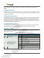
TWR-MCF51CN
User Manual
Rev. 1.1
Freescale Semiconductor Inc.
Microcontroller Solutions Group
Contents
1 Overview ......................................................................................................................................................3
2 Reference Documents..............................................................................................................................4
3 Hardware Features...................................................................................................................................4
3.1 Clocking ..................................................................................................................................................................................4
3.2 System Power.......................................................................................................................................................................4
3.3 Debug Interface ...................................................................................................................................................................4
3.4 RS232 Interface...................................................................................................................................................................5
3.5 Elevator Connections ........................................................................................................................................................5
3.6 Mechanical Form Factor ..................................................................................................................................................5
4 Jumper Table ..............................................................................................................................................5
5 Input/Output Connectors and Pin Usage Table .............................................................................6
6 OSBDM...........................................................................................................................................................7
6.1 Bootloader Mode ................................................................................................................................................................7
6.2 Stand-Alone Debug Interface.........................................................................................................................................7
Revision History
Revision
1.0
Date
May 15, 2009
1.1
July 8, 2009
Changes
Initial Release
Added I/O Connector & Pin Usage table; added OSBDM
section
TWR-MCF51CN User’s Manual
Page 2 of 8
1 Overview
The MCF51CN Tower MCU Module (TWR-MCF51CN) is a low-cost evaluation, demonstration and
development board. The TWR-MCF51CN can operate stand-alone or as the main control board in a
Tower system with peripheral modules.
The following list summarizes the features of the TWR-MCF51CN:
• Tower compatible microcontroller module
• MCF51CN128 in an 80 LQFP package
• MC9S08JM60 based Open Source Debug (OSBDM) circuit
• 4 user controlled LEDs
• Two DIP Switches and three push buttons for user input
• Potentiometer
• MMA7260 three-axis accelerometer
• RS232 transceiver and 2x5 pin header
• Expansion via Primary Elevator connector
A block diagram for the TWR-MCF51CN is shown in the figure below.
Figure 1. TWR-MCF51JCN Block Diagram
TWR-MCF51CN User’s Manual
Page 3 of 8
2 Reference Documents
The documents listed below should be referenced for more information on the Freescale Tower
system and the TWR-MCF51CN. Refer to http://www.freesale.com/tower for the latest revision of all
Tower documentation.
• Freescale Tower Electromechanical Specification
• TWR-MCF51CN Module Pinout
• TWR-MCF51CN Schematics
• TWR-MCF51CN Quick Start Guide
• TWR-MCF51CN-KIT Lab Tutorial
• MCF51CN128 Reference Manual
• MCF51CN128 Data Sheet
• AN3561, USB Bootloader for the MC9S08JM60
3 Hardware Features
This section provides more details about the features and functionality of the TWR-MCF51CN.
3.1 Clocking
Three options are provided for clocking the MCF51CN128 device:
1. 32.768 KHz crystal
2. 25 MHz crystal
3. External clock input from Primary Elevator (CLOCKIN0)
Selection of the clock input is determined by the J11 and J12 settings. The 25 MHz crystal option is
selected by default. Refer to Table 1 for more details.
3.2 System Power
The TWR-MCF51CN can be powered by the OSBDM circuit via the Mini-B USB connector, J14, or a
Functional Elevator via the Mini-B USB connector, J5. A standard USB A male to Mini-B male cable
(supplied) can be used to supply power from a USB Host or powered USB Hub. Optionally, an AC to DC
adapter with a USB A female receptacle (not provided) can be used as the power source.
Power will automatically be sourced from the Elevator connector if power is available on both the
Elevator and the OSBDM.
A jumper, J6, can be used to isolate the 3.3V supply from the microcontroller. This connection can be
used to measure the power usage of the MCF51CN microcontroller.
3.3 Debug Interface
An on-board, MC9S08JM60 based Open Source BDM (OSBDM) circuit provides a debug interface to
the MCF51CN. A standard USB A male to Mini-B male cable (supplied) can be used for debugging via
TWR-MCF51CN User’s Manual
Page 4 of 8
the USB connector, J14. Refer to section x for information on other modes of operation of the
OSBDM.
3.4 RS232 Interface
An RS232 transceiver on the TWR-MCF51CN connects to a standard 2x5 pin header. Selection jumpers
J9 and J10 allow SCI1 signals to be routed to either the RS232 transceiver or the OSBDM circuit. Refer
to Table 1 for more details.
3.5 Elevator Connections
The TWR-MCF51CN features two expansion card-edge connectors that interface to Elevator boards in
a Tower system: the Primary and Secondary Elevator connectors. The Primary Elevator connector,
comprised of sides A and B, is utilized by the TWR-MCF51CN, while the Secondary Elevator connector
only makes connections to ground (GND). The pinout details for the TWR-MCF51CN can be found in
the TWR-MCF51CN Module Pinout document.
3.6 Mechanical Form Factor
The TWR-MCF51CN is designed for the Freescale Tower system and complies with the electrical and
mechanical specification as described in Freescale Tower Electromechanical Specification.
4 Jumper Table
There are several jumpers provided for isolation, configuration, and feature selection. Refer to the
following table for details.
Table 1. TWR-MCF51CN Jumper Table
Jumper
Option
J2
PTD7/RGPIO7/SPSCK2/ADP3
Usage Selection
Setting
1-2
2-3
OFF
1-2
3-4
J3
Analog Isolation Jumpers:
OFF setting isolates signals
from Primary Elevator
5-6
7-8
9-10
11-12
13-14
Description
Connect to DIP Switch Position 1
Connect to Potentiometer
Only connected to Primary Elevator (SPI1_CLK, B7)
Connect PTE2/KBI2P2/SS2/ADP0 to SPI1_CS0 (B9)
and IRQ_D (B59)
Connect PTE1/KBI2P1/MOSI2/ADP1 to SPI1_MOSI
(B10) and IRQ_C (B60)
Connect PTE0/KBI2P0/MISO2/ADP2 to SPI1_MISO
(B11) and IRQ_B (B61)
Connect PTD3/RGPIO3/RXD2/ADP4 to RXD1 (A43)
Connect PTD2/RGPIO2/TXD2/ADP5 to TXD1 (A44)
Connect PTD1/RGPIO1/RXD1/ADP6 to RXD0 (A41)
and J10
Connect PTD0/RGPIO0/TXD1/ADP7 to TXD0 (A42)
and J9
TWR-MCF51CN User’s Manual
Page 5 of 8
1-2
3-4
5-6
7-8
J5
Peripheral Selection Jumpers
9-10
11-12
13-14
ON
J6
MCU Power
J9
UART TXD1 Routing Selection
J10
UART RXD1 Routing Selection
J11
EXTAL Selection
J12
XTAL Selection
J13
MiniBus Latch Enable
J16
OSBDM Bootloader Select
OFF
1-2
2-3
1-2
2-3
1-2
3-4
5-6
1-2
2-3
1-2
2-3
ON
OFF
Connect PTH3/FB_D6/TPM2CH0 to LED4
Connect PTE5/KBI2P5/IRQ/TPM1CH2 to LED3
Connect PTG5/KBI1P5/FB_D3 to LED2
Connect PTE3/KBI2P3/TPM1CH0 to LED1
Connect PTE0/KBI2P0/MISO2/ADP2 to
Accelerometer Z-axis
Connect PTE1/KBI2P1/MOSI2/ADP1to
Accelerometer Y-axis
Connect PTE2/KBI2P2/SS2/ADP0 to Accelerometer
X-axis
Supply 3.3V to MCU
Isolate MCU from Power (current measurement
option)
Route TXD1 to RS232 transceiver
Route TXD1 to OSBDM
Route RXD1 to RS232 transceiver
Route RXD1 to OSBDM
25MHz Crystal
32.768KHz Crystal
CLOCKIN0 from Primary Elevator (B24)
25MHz Crystal
32.768KHz Crystal
Latch Disabled
Latch Enabled
Bootloader mode
Debugger mode
5 Input/Output Connectors and Pin Usage Table
The following tables provides details on which MCF51CN pins are using to communicate with the TWRMCF51CN sensors, LEDs, switches, and other I/O interfaces.
Table 2. I/O Connectors and Pin Usage Table
TWR-MCF51CN
I/O Component
I/O Label
SW1-1
Dip Switch
SW1-2
SW2
Push Button
SW3
SW4 (RST)
LED1
LED2
LED
LED3
LED4
X_OUT
Accelerometer
Y_OUT
MMA7260QT
Z_OUT
Potentiometer
POT
Default Function
PTD7/ RGPIO7
PTH2
PTG6
PTG7
RESETB
PTE3
PTG5
PTE5
FTH3
PTE2
PTE1
PTE0
PTD7/ RGPIO7
MCF51CN128
Alternate 1 Alternate 2
Reserved
SPSCK2
Reserved
FB_D7
KBI1P6
FB_D2
KBI1P7
FB_D1
PTC3
Reserved
KBI2P3
Reserved
KBI1P5
FB_D3
KBI2P5
IRQ
Reserved
FB_D6
KBI2P2
SS2B
KBI2P1
MOSI2
KBI2P0
MISO2
Reserved
SPSCK2
TWR-MCF51CN User’s Manual
Alternate 3
ADP3
TMRCLK1
Reserved
Reserved
Reserved
TPM1CH0
Reserved
TPM1CH2
TPM2CH0
ADP0
ADP1
ADP2
ADP3
Page 6 of 8
RS232
ICL3232
OSBDM
USB to Serial
T1IN
R1OUT
TXD1
RXD1
PTD0/ RGPIO0
PTD1/ RGPIO1
PTD1/ RGPIO1
PTD0/ RGPIO0
Reserved
Reserved
Reserved
Reserved
TXD1
RXD1
RXD1
TXD1
ADP7
ADP6
ADP6
ADP7
Note:
Refer to Section 2.3, Pin Mux Controls, in MCF51CN128 Reference Manual to configure
pin to appropriate alternate function. All pins default to Default Function out of reset.
6 OSBDM
6.1 Bootloader Mode
The MC9S08JM60 device used in the OSBDM circuit is preprogrammed with OSBDM debugger
firmware and a USB Bootloader. Jumper J16 determines which application will run following a poweron reset. If Bootloader Mode is chosen (jumper ON J16), the bootloader will be executed, allowing incircuit reprogramming of the JM60 flash memory via USB. This enables the OSBDM firmware to be
upgraded by the user when upgrades become available. For details on the USB Bootloader, refer to
Application Note AN3561 on the Freescale website (http://www.freescale.com).
The USB Bootloader communicates with a GUI application running on a host PC. The GUI application
can be found on the Freescale website; search keyword “JM60 GUI”. Refer to section 2.5 and 3.3 of
AN3561 for details on installing and running the application.
Note:
The JM60 GUI Installer should be run before connecting the OSBDM in Bootloader
Mode to a host USB port. Otherwise, the JM60 USB device will not be recognized and
the proper drivers will not be loaded.
6.2 Stand-Alone Debug Interface
The OSBDM circuit is designed so that it can program the on-board MCF51CN device, or be isolated
from the on-board circuitry and be used as a programmer for other ColdFire V1 devices. The steps
necessary to operate the OSBDM in this mode are listed here:
1. Remove 0 ohm resistor, SH1
2. Connect J8 (2x3 header) from TWR-MCF51CN to target debug connector
TWR-MCF51CN User’s Manual
Page 7 of 8
Freescale™ and the Freescale logo are trademarks of
Freescale Semiconductor, Inc. All other product or service names
are the property of their respective owners.
© Freescale Semiconductor, Inc. 2009. All rights reserved.
TWR-MCF51CN User’s Manual
Page 8 of 8