1
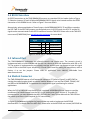
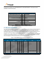
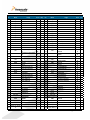
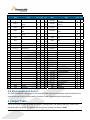
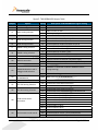
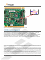
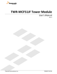
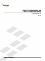
 TWR‐S08MM128 User Manual Rev. 1.0 Freescale Semiconductor Inc. Contents 1 Overview ...................................................................................................................................................... 3 2 Reference Documents .............................................................................................................................. 4 3 Hardware Features ................................................................................................................................... 4 3.1 Clocking .................................................................................................................................................................................. 4 3.2 System Power ....................................................................................................................................................................... 4 3.3 Debug Interface ................................................................................................................................................................... 4 3.4 RS232 Interface ................................................................................................................................................................... 5 3.5 Infrared Port ......................................................................................................................................................................... 5 3.6 Medical Connector .............................................................................................................................................................. 5 3.7 Elevator Connections ........................................................................................................................................................ 6 3.8 Mechanical Form Factor .................................................................................................................................................. 8 4 Jumper Table .............................................................................................................................................. 8 5 Input/Output Connectors and Pin Usage Table ........................................................................... 10 6 OSBDM ........................................................................................................................................................ 11 6.1 Bootloader Mode For MC9S08JM60 ........................................................................................................................ 11 7 Bootloader Mode For MC9S08MM128 ............................................................................................ 11 8 BDM inteface (Optional) ...................................................................................................................... 12 TWR‐MC9S08MM128 User Manual Page 2 of 13 1 Overview TWR‐S08MM128 is a low‐cost evaluation, demonstration and development board that features an 8‐
bit MC9S08MM128 microcontroller. The TWR‐S08MM128 can operate stand‐alone or as the main control board in a Tower System with peripheral modules. The following list summarizes the features of the MC9S08MM Tower MCU board: • Tower compatible processor board • Open Source BDM (OSBDM) circuit • Analog measurement circuitry • 4 LEDs • DIP Switches and push buttons for user input • Potentiometer • MMA7361L three‐axis accelerometer • RS232 transceiver and 2x5 pin header Figure 1. TWR‐S08MM128 Block Diagram TWR‐MC9S08MM128 User Manual Page 3 of 13 2 Reference Documents The documents listed below are available online. Refer to http://www.freescale.com/tower for the latest revision of all Tower System documentation. • TWR‐S08MM128 Schematics • TWR‐S08MM128 Quick Start Guide • TWR‐S08MM128‐KIT Lab Tutorial • MC9S08MM128 Reference Manual • MC9S08MM128 Data Sheet • AN3561, USB Bootloader for the MC9S08JM60 3 Hardware Features This section provides more details about the features and functionality of the TWR‐S08MM128. 3.1 Clocking Two crystals are provided on the board for clocking the MC9S08MM128 device: 1. A 16 MHz crystal connected to XTAL2 and EXTAL2 for system clocking 2. A 32.768kHz crystal connected to XTAL1 and EXTAL1 for TOD usage 3.2 System Power The TWR‐S08MM128 can be powered by the Open Source BDM (OSBDM) circuit via the Mini‐B USB connector when stand‐alone. When assembled with the Tower System and the TWR‐SER is configured to run USB device mode (J16 pin 3 and 4 connected), the Mini‐B USB connector is no longer used as a power source and only used for OSBDM debugging purposes. In this case, the power will be supplied from the Mini‐B USB from the TWR‐SER. Please plug in the Mini‐B USB connector from TWE‐SER before plugging in the Mini‐B USB connector from TWR‐S08MM128. A standard USB A male to Mini‐B male cable (provided) can be used to supply power from a USB host or powered USB hub. Optionally, an AC to DC adapter with a USB A female receptacle (not provided) can be used as the power source. A jumper, J11, can be used to isolate the 3.3V supply from the microcontroller. This connection can be used to measure the power usage of the MC9S08MM128 microcontroller. 3.3 Debug Interface An on‐board, MC9S08JM60 based OSBDM circuit provides a debug interface to the MC9S08MM128. A standard USB A male to Mini‐B male cable (provided) can be used for debugging via the USB connector, J17. Refer to Section 6 for information on other modes of operation of the OSBDM. TWR‐MC9S08MM128 User Manual Page 4 of 13 3.4 RS232 Interface An RS232 transceiver on the TWR‐S08MM128 connects to a standard 2x5 pin header (refer to Figure 2). Selection jumpers J15 and J16 allow MC9S08MM128 SCI2 signals to be routed to either the RS232 transceiver or the OSBDM circuit. Refer to Figure 5 for more details. Alternatively, when assembled as a Tower System, the MC9S08MM128 SCI1 TX and RX are routed to the SER‐TWR. If the SER‐TWR jumpers are configured to run in RS‐232 mode, the SCI1 TX and the RX signal can be communicated via the RS232 connector from the TWR‐SER. Please refer to the TWR‐SER user manual (TWRSERUM) from www.freescale.com/tower for more detail. MC9S08MM128 Signal Not Connected
TX2
RX2
Not Connected
GND
MC9S08MM128 Pin Signal 1 2 Not Connected 3 4 Not Connected 5 6 Not Connected 7 8 Not Connected 9 10 3.3V Figure 2. RS232 2x5 Pin Header Connections 3.5 Infrared Port The TWR‐S08MM128 implements an infrared transmit and receive port. The transmit circuit is implemented with an infrared diode and the user can choose to drive the diode either with IRO or SCI TX. The receiver is implemented by an infrared transistor and the user can choose to input this signal to the SCI RX or the ACMP input. Jumpers J9, J25 and J26 are used for routing the connections, refer to Section 4 to set the jumpers. Please refer to application note AN4116, searchable from www.freescale.com 3.6 Medical Connector The TWR‐S08MM128 features a 2x10 expansion connector J27 (refer to Figure 3) to MED‐EKG for routing the medical engine signals to external medical board so it can use the OPAMP, TRIAMP, ADC and DAC on MC9S08MM128 to implement the requirement signal conditioning for medical applications. When the DSC MC56F8006 from the MED‐EKG is enabled, MC9S08MM128 can choose to read the conditioned EKG results output from the DSC via I2C transmission (pin 3 and pin 4). To enable I2C communication, you must assemble the MEG‐EKG with the Tower System because the TWR‐SER has the pulled up resistors circuit required for I2C transmission. In Figure 3, the bold text highlights the functions that are used to implement the MED‐EKG demonstration. For detail about the MED‐EKG, please refer to the MED‐EKG user manual, MED‐EKG lab TWR‐MC9S08MM128 User Manual Page 5 of 13 and schematic included in the TWR‐S08MM128‐KIT or TWR‐MCF51MM‐KIT. All of these are also available on Freescale.com/tower TWR‐S08MM128 Signal MOSFET Q6 (pin 3)‐Power (3.3V) PTD4/SDA/TPM1CH2
DADP0
PTC4/KBI1P7/CMPP0/ADP8
OUT1
INP1‐
PTA4/INP1+
VINP1 VINN1/DADM2
TRIOUT1/DADP2
Pin 1 3 5 7 9 11 13 15 17 19 2 4 6 8 10 12 14 16 18 20 TWR‐S08MM128 Signal Ground(GND) PTD5/SCL/ TPM1CH3 DADM0 DACO_E OUT2 INP2‐ PTA7/INP2+ VINP2 VINN2/DADM3 TRIOUT2/DADP3 Figure 3. Medical Connector 2x10 Pin Header Connections 3.7 Elevator Connections The TWR‐S08MM128 features two expansion card‐edge connectors that interface to elevator boards in a Tower System: the Primary and Secondary Elevator connectors. The Primary Elevator connector, comprised of sides A and B, is utilized by the TWR‐S08MM128, while the Secondary Elevator connector only makes connections to ground (GND). Figure 4 provides the pinout for the Primary Elevator connector. An “X” in the “Used” column indicates that there is a connection from the TWR‐S08MM128 to that pin on the elevator connector. An “X” in the “Jmp” column indicates that a jumper is available that can configure or isolate the connection from the elevator connector. Figure 4. TWR‐S08MM128 Primary Elevator Connector Pinout TWR‐S08MM128 Primary Connector Pin B1 B2 B3 B4 B5 B6 B7 B8 B9 B10 B11 Name 5V GND 3.3V ELE_PS_SENSE GND GND SPI1_CLK SPI1_CS1 SPI1_CS0 SPI1_MOSI SPI1_MISO Usage 5.0V Power Ground 3.3V Power Elevator Power Sense Ground Ground PTG0/SPSCK1 PTA0/SS1_b PTF6/MOSI1 PTF7/MISO1 Used Jmp Pin X A1 X A2 X A3 X A4 X A5 X A6 X A7 A8 X A9 X A10 X Name 5V GND 3.3V 3.3V GND GND SCL0 SDA0 Usage 5.0V Power Ground 3.3V Power 3.3V Power Ground Ground PTD5/SCL/TPM1CH3 PTD4/SDA/TPM1CH2 GPIO9 / OPEN PTE4/CMPP3/TPMCLK/IRQ GPIO8 / OPEN PTC7/KBI2P2/CLKOUT/ADP11 PTC6/KBI2P1/PRACMPO/ADP1
A11 GPIO7 / OPEN 0 TWR‐MC9S08MM128 User Manual Used Jmp X X X X X X X X X X X Page 6 of 13 TWR‐S08MM128 Primary Connector Pin B12 B13 B14 B15 B16 B17 B18 B19 B20 B21 B22 B23 B24 B25 B26 B27 B28 B29 B30 B31 B32 B33 B34 B35 B36 B37 B38 B39 B40 B41 B42 B43 B44 B45 B46 B47 B48 B49 B50 B51 B52 Name ETH_COL ETH_RXER ETH_TXCLK ETH_TXEN ETH_TXER ETH_TXD3 ETH_TXD2 ETH_TXD1 ETH_TXD0 GPIO1 / OPEN GPIO2 / OPEN GPIO3 / OPEN CLKIN0 CLKOUT1 GND AN7 AN6 AN5 AN4 GND DAC1 TMR3 TMR2 GPIO4 3.3V PWM7 PWM6 PWM5 PWM4 CANRX0 CANTX0 CAN SPI0_MISO SPI0_MOSI SPI0_CS0 SPI0_CS1 SPI0_CLK GND SCL1 SDA1 Usage PTA2/KBI1P1/RX1/ADP4 PTA6 PTB1/BLMS_b Ground PTC5/KBI2P0/CMPP1/AD
P9 PTC4/KBI1P7/CMPP0/AD
P8 PTC3/KBI1P6/SS2/ADP7 PTC2/KBI1P5/SPSCK2/AD
P6 Ground VREFO PTD5/SCL/TPM1CH3 PTD4/SDA/TPM1CH2 3.3V Power PTD5/SCL/TPM1CH3 PTD4/SDA/TPM1CH2 PTD3/TPM1CH1 PTD2/TPM1CH0 PTF7/MISO1 PTF6/MOSI1 PTA0/SS1_b PTG0/SPSCK1 Ground GPIO5 / OPEN PTA3/KBI1P2/ADP5 USB0_DP_PDOW
B53 N Used Jmp Pin A12 A13 A14 A15 A16 A17 A18 A19 A20 X A21 X A22 X A23 A24 A25 X A26 Name ETH_CRS ETH_MDC ETH_MDIO ETH_RXCLK ETH_RXDV ETH_RXD3 ETH_RXD2 ETH_RXD1 ETH_RXD0 SSI_MCLK SSI_BCLK SSI_FS SSI_RXD SSI_TXD AN3 X X X X X X X X X X X X X X X X X X X A27 A28 A29 GND AN2 AN1 Usage VINN1/DADM2 TRIOUT2/DADP3 TRIOUT1/DADP2 OUT1 Ground Used Jmp X X X X X DADM0 X DADP0 VINP2 X X AN0 A30 VINN2/DADM3 A31 GND Ground DAC0 A32 DACO_E TMR1 A33 PTD3/TPM1CH1 TMR0 A34 PTD2/TPM1CH0 A35 GPIO6 A36 3.3V 3.3V Power PWM3 A37 PTE7/TPM2CH3 PWM2 A38 PTF0/TPM2CH2 PWM1 A39 PTF1/RX2/TPM2CH1 PWM0 A40 PTF2/TX2/TPM2CH0 RXD0 A41 TXD0 A42 RXD1 A43 PTD7/RX1 TXD1 A44 PTD6/TX1 A45 BKGD A46 ALLPST A47 JTAG_EN A48 TRST_b / DSCLK A49 GND Ground A50 TCLK / DSCLK A51 TDI / DSI A52 TDO / DSO X X X X X X X X X X X X X A53 TMS / BKPT_b TWR‐MC9S08MM128 User Manual Page 7 of 13 X TWR‐S08MM128 Primary Connector Pin Name Usage USB0_DM_PDOW
B54 N PTC6/KBI2P1/PRACMPO/
IRQ_H B55 ADP10 PTC7/KBI2P2/CLKOUT/A
IRQ_G B56 DP11 PTC7/KBI2P2/CLKOUT/A
IRQ_F B57 DP11 PTC6/KBI2P1/PRACMPO/
IRQ_E B58 ADP10 PTE4/CMPP3/TPMCLK/IR
IRQ_D B59 Q PTE4/CMPP3/TPMCLK/IR
IRQ_C B60 Q IRQ_B B61 PTA3/KBI1P2/ADP5 IRQ_A B62 PTA2/KBI1P1/RX1/ADP4 EBI_ALE / B63 EBI_CS1_b PTE0/KBI2P3 EBI_CS0_b B64 PTC0/MOSI2 B65 GND Ground B66 EBI_AD15 PTB6/KBI1P3 B67 EBI_AD16 B68 EBI_AD17 B69 EBI_AD18 EBI_AD19 B70 EBI_R/W_b MCU_RXD1 B71 EBI_OE_b B72 EBI_D7 B73 EBI_D6 B74 EBI_D5 B75 EBI_D4 B76 EBI_D3 B77 EBI_D2 B78 EBI_D1 B79 EBI_D0 B80 B81 B82 GND 3.3V Ground 3.3V Power Used Jmp X X X X X X X X X X X X X X X X X X X X X X X X X X X X X Pin A54 A55 A56 A57 A58 A59 A60 A61 A62 A63 A64 A65 A66 A67 A68 A69 A70 A71 A72 A73 A74 A75 A76 A77 A78 A79 A80 A81 A82 Name USB_DM USB_DP USB_ID USB_VBUS Usage USB_DM X USB_DP X VBUS TMR7 OUT2 TMR6 INP1‐ TMR5 INP2‐ TMR4 RSTIN_b Used Jmp X X X X X PTA4/INP1+ RSTOUT_b CLKOUT0 GND EBI_AD14 EBI_AD13 EBI_AD12 EBI_AD11 EBI_AD10 EBI_AD9 EBI_AD8 EBI_AD7 EBI_AD6 EBI_AD5 EBI_AD4 EBI_AD3 EBI_AD2 EBI_AD1 EBI_AD0 GND 3.3V PTC7/KBI2P2/CLKOUT/ADP11 Ground MCU_TXD1 PTA3/KBI1P2/ADP5 PTF3/SCL PTF4/SDA PTF5/KBI2P7 PTA0/SS1_b PTA1/KBI1P0/TX1 PTC1/MISO2 Ground 3.3V Power X X X X X X X X X X X X X X X X X X X 3.8 Mechanical Form Factor The TWR‐S08MM128 is designed for the Freescale Tower System and complies with the electrical and mechanical specification as described in Freescale Tower Electromechanical Specification. 4 Jumper Table There are several jumpers provided for isolation, configuration, and feature selection. Refer to the following table for details. The default installed jumper settings are shown in bold. TWR‐MC9S08MM128 User Manual Page 8 of 13 Figure 5. TWR‐S08MM128 Jumper Table Jumper J1 J2 DADP0 routing selection DADM0 routing selection J3 VINP1 routing selection J4 Potentiometer connection J5 DACO routing selection J6 DACO routing selection J7 TRIAMP routing selection J8 TRIAMP routing selection J9 Infrared receive routing J10 USB3.3V connection J11 MCU IDD measure J12 OSBDM Bootloader mode or debugger mode selection 1‐2 1‐2 1‐2 2‐3 1‐2 1‐2 2‐3 1‐2 1‐2 2‐3 1‐2 2‐3 1‐2 1‐2 2‐3 1‐2 J14 BDM connector for MC9S08MM128 BDM connector for JM60 J15 SCI2 TXD Routing Selection J16 SCI2 RXD Routing Selection J18 LED & Accelerometer connections J19 Accelerometer mode control J13 Setting
Option Description of MC9S08MM128 signal routing Connect DADP0 to medical connector J27 pin 5 Connect DADM0 to medical connector J27 pin 6 VINP1 connect to GND VINP1 optionally connected to DACO Connection of ADP4 to potentiometer Connect DACO to VINP1 if pin 2‐3 of J3 is connected Connect DACO to a RC low pass filter Connect DACO to medical connector J27 pin 8 Connect TRIOUT1 to TRIOUT_SEL2 Connect TRIOUT2 to TRIOUT_SEL2 Connect TRIOUT1 to TRIOUT_SEL1 Connect TRIOUT2 to TRIOUT_SEL1 Connect Infrared transistor output to CMPP1 USB3.3V connects to external 3.3V power supply USB3.3V connects to on‐chip USB 3.3V regulator output For measuring MC9S08MM128 current OSBDM IC in bootloader mode(For OSBDM firmware 1‐2 reprogramming) Open OSBDM IC in debugger mode . Open BDM connector for MC9S08MM128 Open 1‐2 2‐3 1‐2 2‐3 1‐2 3‐4 5‐6 7‐8 9‐10 11‐12 13‐14 1‐2 BDM connector for MC9S08JM60 Connect TX2 to the RS232 transceiver Connect TX2 to the OSBDM debugger interface circuit Connect RX2 to the RS232 transceiver Connect RX2 to the OSBDM debugger interface circuit Connects LED4 to pin PTE7/TPM2CH3 Connects LED3 to pin PTF0/TPM2CH2 Connects LED2 to pin PTF1/RX2/TPM2CH1 Connects LED1 to pin PTF2/TX2/TPM2CH0 Connects ADP8 to ACCZ Connects ADP7 to ACCY Connects ADP6 to ACCX Connects PTA3 to SELF TEST pin of accelerometer 3‐4 Connects PTA6 to SLEEP pin of accelerometer 5‐6 Connects PTA5 to G‐SELECT pin of accelerometer TWR‐MC9S08MM128 User Manual Page 9 of 13 J20 J21 J24 Accelerometer control RS232 connector Infrared filter connection J25 Infrared transmit routing J26 Infrared transmit routing J27 Medical board connector 1‐2 Open 1‐2 1‐2 3‐4 5‐6 1‐2 2‐3 Open Connects PTB0 to 0G‐DETECT pin of accelerometer 2x5 RS232 connector Choose whether to filter Infrared output Connects Infrared transistor output to ADP10 Connects Infrared transistor output to RX1 Connects either IRO or TX1 to Infrared diode base on J26 TX1 pin drives Infrared transmit IRO pin drives Infrared transmit Connects to MED‐EKG board NOTE: For more detail, please refer to TWR‐S08MM128 schematics available in the TWR‐S08MM128‐KIT or on Freescale.com/tower. 5 Input/Output Connectors and Pin Usage Table The following tables provide details on which MC9S08MM128 pins are communicating with the TWR‐
MC9S08MM sensors, LEDs, switches and other I/O interfaces. Figure 6. I/O Connectors and Pin Usage Table TWR‐S08MM128 I/O Component I/O Label Dip Switch Push Button LED Accelerometer MMA7361L Potentiometer RS232 ICL3232 SW3‐1&4 SW3‐2&3 SW1 SW2 SW4 LED1 (D9) LED2(D10) LED3(D11) LED4(D12) X_OUT Y_OUT Z_OUT POT 232_RXD 232_TXD Default
PTA5 PTB1 PTD1 PTC6 PTE4 PTF2 PTF1 PTF0 PTE7 PTC2 PTC3 PTC4 PTA2 PTE6 PTE5 MC9S08MM128 Alt 1 Alt 2 ‐ /BLMS CMPP2 KBI2P1 CMPP3 TX2 RX2 TPM2CH2 TPM2CH3 KBI1P5 KBI1P6 KBI1P7 KBI1P1 RX2 TX2 ‐ ‐ /RESET PRACMPO TPMCLK TPM2CH0 TPM2CH1 ‐ ‐ SPSCK2 /SS2 CMPP0 RX1 ‐ ‐ Alt 3 ‐ ‐ ‐ ADP10 IRQ ‐ ‐ ‐ ‐ ADP6 ADP7 ADP8 ADP4 ‐ ‐ NOTE: LED1 to LED4 are labelled as D9 to D12 on the TWR‐S08MM128 silkscreen. TWR‐MC9S08MM128 User Manual Page 10 of 13 6 OSBDM An on‐board, MC9S08JM60 based OSBDM circuit provides a debug interface to the MC9S08MM128. The MC9S08JM60 is a USB‐enabled microcontroller with an 8‐bit HC9S08 core. The OSBDM circuit provides a USB‐to‐debug interface that allows run‐control and debugging of the MC9S08MM128 target device. The USB drivers required to communicate with the OSBDM are provided in development tools such as Freescale CodeWarrior. When TWR‐S08MM128 is used stand‐alone, this single USB connection can also be used for power. 6.1 Bootloader Mode For MC9S08JM60 The MC9S08JM60 device used in the OSBDM circuit is preprogrammed with OSBDM debugger firmware and a USB Bootloader. The bootloader mode can be used to update the OSBDM debugger firmware if an update becomes available. Jumper J12 determines which application will run following a power‐on reset. If the Bootloader Mode is chosen (jumper shunt on J12), the bootloader will be executed, allowing in‐circuit reprogramming of the JM60 flash memory via USB. Refer to Application Note AN3561 on the Freescale website (http://www.freescale.com) for details on the USB Bootloader. The USB Bootloader communicates with a GUI application running on a host PC. The GUI application can be found on the Freescale website; search keyword “JM60 GUI.” Refer to section 2.5 and 3.3 of AN3561 for details on installing and running the application. Note: The JM60 GUI Installer should be run before connecting the OSBDM in Bootloader Mode to a host USB port. Otherwise, the JM60 USB device will not be recognized and the proper drivers will not be loaded. 7 Bootloader Mode For MC9S08MM128 Unlike MC9S08JM60, MC9S08MM128 has an on‐chip ROM based USB bootloader that allows the MC9S08MM128 for mass erase and programming via its USB interface. This on‐chip bootloader does not consume user flash space. To enable USB bootloader mode for MC9S08MM128, on the TWR‐
S08MM128 module, set SW3 DIP switch 2 and 3 to position 3, as indicated in Figure 7. NOTE: Under normal development you will need to set SW3 DIP switch 2 and 3 to position 2. TWR‐MC9S08MM128 User Manual Page 11 of 13 Figure 7. Setting SW3 for MC9S08MM128 USB bootloader mode 8 BDM inteface (Optional) Both MC9S08MM128 and MC9S08JM60 have an on‐chip background debug module. The user can choose to bypass the USB OSBDM interface and use the BDM interface for debugging and programming the corresponding chip instead. The BDM interface for MC9S08MM128 is at J13 header and MC9S08JM60 is at J14 from the TWR‐S08MM128 module. The user needs a P&E USB BDM MULTILINK in order to use this interface. This is a repeat function of the OSBDM and is not required. Information in this document is provided solely to enable system and software implementers to use Freescale Semiconductor products. There are no express or implied copyright licenses granted hereunder to design or fabricate any integrated circuits or integrated circuits based on the information in this document. Freescale Semiconductor reserves the right to make changes without further notice to any products herein. Freescale Semiconductor makes no warranty, representation, or guarantee regarding the suitability of its products for any particular purpose, nor does Freescale Semiconductor assume any liability arising out of the application or use of any product or circuit, and specifically disclaims any liability, including without limitation consequential or incidental damages. “Typical” parameters that may be provided in Freescale Semiconductor data sheets and/or specifications can and do vary in different applications and actual performance may vary over time. All operating parameters, including “Typicals,” must be validated for each customer application by customer’s technical experts. Freescale Semiconductor does not convey any license under its patent rights nor the rights of others. Freescale Semiconductor products are not designed, intended, or authorized for use as components in systems intended for surgical implant into the body, or other applications intended to support or sustain life, or for any other application in which failure of the Freescale Semiconductor product could create a situation where personal injury or death may occur. Should Buyer purchase or use Freescale Semiconductor products for any such unintended or TWR‐MC9S08MM128 User Manual Page 12 of 13 unauthorized application, Buyer shall indemnify Freescale Semiconductor and its officers, employees, subsidiaries, affiliates, and distributors harmless against all claims, costs, damages, and expenses, and reasonable attorney fees arising out of, directly or indirectly, any claim of personal injury or death associated with such unintended or unauthorized use, even if such claims alleges that Freescale Semiconductor was negligent regarding the design or manufacture of the part. RoHS‐compliant and/or Pb‐free versions of Freescale products have the functionality and electrical characteristics as their non‐RoHS‐complaint and/or non‐Pb‐free counterparts. For further information, visit freescale.com or contact your Freescale sales representative. For information on Freescale’s Environmental Products program, visit freescale.com/epp. Freescale™ and the Freescale logo are trademarks of
Freescale Semiconductor, Inc. All other product or service names
are the property of their respective owners.
© Freescale Semiconductor, Inc. 2010. All rights reserved.
TWR‐MC9S08MM128 User Manual Page 13 of 13