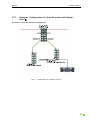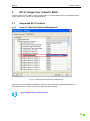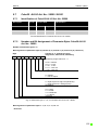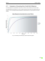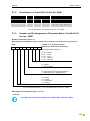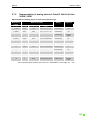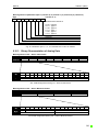
1
|Manual Cube67+ BN-P | Installation | Startup | Diagnostics | Technical Data | DPV1 Support | Modules Manual Cube67+ | BN-P Publisher's Note Instruction manual for Cube67+ BN-P (Article Number: 56521) Version 2.8 Edition 08_12 EN Manual Number 56521 Murrelektronik GmbH Falkenstrasse 3 D-71570 Oppenweiler Phone +49 (0) 7191 47-0 Fax +49 (0) 7191 47-130 [email protected] 2 Manual Cube67+ | BN-P Service and Support Website: www.murrelektronik.com In addition, our Customer Service Center (CSC) will be glad to assist you: Our Customer Service Center can support you throughout your project in the planning and conception of customer applications, configuration, installation, and startup. We also offer competent consulting or – in more complex cases – we even provide direct onsite support. The Customer Service Center provides support tools. It performs measurements for fieldbus systems, such as PROFIBUS DP, DeviceNet, CANopen, and AS interface, as well as energy, heat, and EMC measurements. Our coworkers at the Customer Service Center provide their competence, know-how, and years of experience. They are knowledgeable about hardware and software, and compatibility with products made by various manufacturers. You can contact the Customer Service Center at Phone +49 (0) 71 91 47-424 or by email at [email protected]. 3 Manual Cube67+ | BN-P About the User Manual and its Structure 4 Manual Cube67+ | BN-P Here are links to the bus user manuals: >>> PROFIBUS (www.PROFIBUS.com) >>> IO-Link IO link (www.io-link IO link.com) 5 Manual Cube67+ | BN-P Table of Contents Publisher's Note ...................................................................................................................................... 2 Service and Support ................................................................................................................................ 3 About the User Manual and its Structure ................................................................................................ 4 Table of Contents .................................................................................................................................... 6 Important Information ............................................................................................................................ 15 1 Description of the Cube67+ ...................................................................................................... 17 2 Installation ................................................................................................................................ 17 2.1 Mounting ................................................................................................................................. 17 2.2 Overview of Connections Cube67+ BN-P Art. No. 56521 ..................................................... 18 Startup ...................................................................................................................................... 19 3 3.1 Internal System Connection Features .................................................................................... 19 3.2 Internal System Connection Terminations .............................................................................. 20 3.3 Terminating PROFIBUS Segments ........................................................................................ 20 3.4 Assigning and Setting the PROFIBUS Address ..................................................................... 20 3.5 GSD File.................................................................................................................................. 21 3.6 Baud Rates ............................................................................................................................. 21 3.7 Configuration and Parameter .................................................................................................. 22 3.7.1 Maximum lengths of telegrams ........................................................................................ 22 3.7.2 Assigning Slots / Real Module ......................................................................................... 22 3.7.3 Example : Configuration of a Cube20 system with Simatic Step7 ............................... 26 3.7.4 Cube67+ BN-P Art. No. 56521 ........................................................................................ 29 Diagnostics ............................................................................................................................... 33 4 4.1 4.1.1 Meaning of "Bus Run" LED States .................................................................................. 33 4.1.2 Meaning of "Cfg F" LED States ....................................................................................... 34 4.1.3 Meaning of US and UA LED states ................................................................................. 35 4.1.4 Meaning of US / UA LED States at Internal System Connection Sockets ...................... 36 4.2 Diagnostics via the Fieldbus ................................................................................................... 38 4.2.1 Standard Diagnostic Information Format ......................................................................... 40 4.2.2 Identification-Related Diagnostic ..................................................................................... 43 4.2.3 Device-Related Diagnostic .............................................................................................. 44 4.2.4 Channel-Related Diagnostic ............................................................................................ 45 4.3 5 LED Indicators ........................................................................................................................ 33 Troubleshooting ...................................................................................................................... 47 DP-V1 Support for Cube67+ BN-P ........................................................................................... 49 6 Manual 5.1 Cube67+ | BN-P Supported DP-V1 Indices ....................................................................................................... 49 5.1.1 Index 10 "Machine Options Management" ...................................................................... 49 5.1.2 Index 12 "BusControl" ...................................................................................................... 52 5.1.3 Index 13 "Machine Options Management Configuration Test"........................................ 53 5.1.4 Index 255 Identification and Maintenance (I&M) ............................................................. 53 Machine Options Management ................................................................................................ 58 6 6.1 Maximum Configuration .......................................................................................................... 58 6.2 Selecting Modules and Setting a Configuration ...................................................................... 58 6.3 Configuration Test ................................................................................................................... 60 6.4 Changing a Module ................................................................................................................. 60 Technical Data of Cube67+ BN-P Art. No. 56521 .................................................................... 63 7 7.1 Signal Delay of Digital Inputs and Outputs ............................................................................. 63 7.2 Signal Delay of Analog Inputs and Outputs ............................................................................ 63 7.3 Technical Data ........................................................................................................................ 64 Cube67+ Modules .................................................................................................................... 66 8 8.1 Cube67+ DIO12 IOL4 E 8xM12 Art. No. 56752 ..................................................................... 66 8.1.1 Identification ..................................................................................................................... 67 8.1.2 Baud Rates ...................................................................................................................... 67 8.1.3 Parameters ...................................................................................................................... 68 8.1.4 Data Cube67+ DIO12 IOL4 E 8xM12 .............................................................................. 77 8.1.5 I&M Functions of Cube67+ DIO12 IOL4 E 8xM12 ......................................................... 78 8.2 Cube67+ DIO4 RS232/485 E 4xM12 Art. No. 56761 ............................................................. 79 8.2.1 Identification ..................................................................................................................... 80 8.2.2 SEW-MOVILINK Useful Data Protocol ............................................................................ 81 8.2.3 Parameters ...................................................................................................................... 82 8.2.4 DIO Data of Cube67+ DIO4 RS232/485 E 4xM12 .......................................................... 95 8.2.5 Communication Data of Cube67+ DIO4 RS232/485 E 4xM12 ....................................... 96 8.2.6 I&M Functions of Cube67+ DIO4 RS232/485 E 4xM12 ................................................ 100 8.3 Cube67+ DIO12 IOL4 E 8xM12 Art. No. 56765 ................................................................... 101 8.3.1 Identification ................................................................................................................... 102 8.3.2 Baud rates ..................................................................................................................... 102 8.3.3 Parameters .................................................................................................................... 103 8.3.4 Data Cube67+ DIO12 IOL4 E 8xM12 ............................................................................ 113 8.3.5 I&M Functions of Cube67+ DIO12 IOL4 E 8xM12 ........................................................ 114 Cube20-Module ...................................................................................................................... 115 9 9.1 Cube20 BN67 DIO8 – Art. No. 56450 ................................................................................... 115 9.1.1 Identification ................................................................................................................... 115 7 Manual Cube67+ | BN-P 9.1.2 Bit assignment I/O - Data............................................................................................... 115 9.1.3 Parameterization ............................................................................................................ 116 9.1.4 Bit Assignment of the Parameter Bytes ......................................................................... 116 9.2 Cube20 DI32 Art. No.: 56112................................................................................................ 117 9.2.1 Identification ................................................................................................................... 117 9.2.2 Number and Bit Assignment of Parameter Bytes .......................................................... 117 9.2.3 bit assignment I/O – Data – Input data IDM .................................................................. 117 9.3 Cube20 DO16 Art. No.: 56117 .............................................................................................. 118 9.3.1 Identification ................................................................................................................... 118 9.3.2 Number and Bit Assignment of Parameter Bytes .......................................................... 118 9.3.3 Bit Assignment I/O – Data – Input data IDM.................................................................. 118 9.4 Cube20 DO32 Art. No.: 56118 .............................................................................................. 119 9.4.1 Kennung ........................................................................................................................ 119 9.4.2 Number and Bit Assignment of Parameter Bytes .......................................................... 119 9.4.3 Bit assignment I/O – Data – Output Data ODM ............................................................. 119 9.5 Cube20 DI32 NPN / PNP Art. No. 56121 ............................................................................. 120 9.5.1 Identification ................................................................................................................... 120 9.5.2 Number and Bit Assignment of Parameter Bytes .......................................................... 120 9.5.3 Bit assignment I/O-Data – Input Data IDM .................................................................... 120 9.6 Cube20 DI16 DO16 Art. No.: 56168 ..................................................................................... 121 9.6.1 Identification ................................................................................................................... 121 9.6.2 Number and Bit Assignment of Parameter Bytes .......................................................... 121 9.6.3 Bit assignment I/O - Data............................................................................................... 121 9.7 Cube20 AI4 U/I Art. No.: 56200 / 56201 .............................................................................. 122 9.7.1 Identification of Cube20 AI4 U/I Art.-No. 56200 ............................................................ 122 9.7.2 Number and Bit Assignment of Parameter Bytes Cube20 AI4 U/I Art. No.: 56200 ....... 122 9.7.3 Explanation of Smoothing (Only Cube20 AI4 U/I Modules) .......................................... 123 9.7.4 Identification of Cube20 AI4 U/I Art.-No. 56201 ............................................................ 124 9.7.5 Number and Bit Assignment of Parameter Bytes Cube20 AI4 U/I Art. No.: 56201 ....... 124 9.7.6 Delta Value (Only Cube20 AI4 U/I Art.-No.: 56201) ...................................................... 125 9.7.7 Binary Representation of the Analog Data of Cube20 AI4 U/I Art.-No.: 56200 / 56201126 9.7.8 Representation of analog values of Cube20 AI4 U/I Art.-No.: 56200 / 56201.............. 127 9.8 Cube20 AO4 U/I Art. No.: 56220 / 56221 ............................................................................ 130 9.8.1 Identification of Cube20 AO4 U/I Art.-No. 56220 .......................................................... 130 9.8.2 Number and Bit Assignment of Parameter Bytes Cube20 AO4 U/I Art. No.: 56220 ..... 130 9.8.3 Identification of Cube20 AO4 U/I Art. No. 56221 ........................................................... 131 9.8.4 Number and Bit Assignment of Parameter Bytes Cube20 AO4 U/I Art. No.: 56221 ..... 131 8 Manual Cube67+ | BN-P 9.8.5 Binary Representation of the Analog Data of Cube20 AO4 U/I Art. No.: 56220 / 56221 132 9.8.6 Representation of Analog Values of Cube20 AO4 U/I Art. No.: 56220 / 56221 ............ 133 9.9 Cube20 AI4 RTD Art. No.: 56230 ......................................................................................... 135 9.9.1 Identification ................................................................................................................... 135 9.9.2 Number and Bit Assignment of Parameter Bytes .......................................................... 135 9.9.3 Binary Representation of Analog Data .......................................................................... 136 9.9.4 Representation of Analog Values of Cube20 AI4 RTD Art. No.: 56230 ........................ 137 Cube20 AI4 TH Art. No.: 56240 ........................................................................................ 140 9.10 9.10.1 Identification ................................................................................................................... 140 9.10.2 Number and Bit Assignment of Parameter Bytes .......................................................... 140 9.10.3 Binary Representation of Analog Data .......................................................................... 141 9.10.4 Representation of Analog Values of Cube20 AI4 TH Art. No.: 56240 ........................... 142 Cube67 Digital I/O Modules ................................................................................................... 147 10 10.1 DIO16 C 8xM12 – Art.Nr. 56600 ....................................................................................... 147 10.1.1 Identification ................................................................................................................... 147 10.1.2 Bit Assignment I/O - Data .............................................................................................. 147 10.1.3 Parameterization ............................................................................................................ 148 10.2 DIO16 E 8xM12 – Art.Nr. 56601xx .................................................................................... 150 10.2.1 Identification ................................................................................................................... 150 10.2.2 Bit Assignment I/O - Data .............................................................................................. 150 10.2.3 Parameterization ............................................................................................................ 151 10.3 DI16 C 8xM12 – Art.Nr. 56602 .......................................................................................... 153 10.3.1 Identification ................................................................................................................... 153 10.3.2 Bit Assignment I/O - Data .............................................................................................. 153 10.3.3 Parameterization ............................................................................................................ 153 10.4 DI16 E 8xM12 – Art.Nr. 56603xx ...................................................................................... 156 10.4.1 Identification ................................................................................................................... 156 10.4.2 Bit Assignment I/O - Data .............................................................................................. 156 10.4.3 Parameterization ............................................................................................................ 156 10.5 DO12 E 6xM12 K3 – Art.Nr. 56605 ................................................................................... 159 10.5.1 Identification ................................................................................................................... 159 10.5.2 Bit Assignment I/O - Data .............................................................................................. 159 10.5.3 Parameter bytes ............................................................................................................ 159 10.6 DI16 E 8xM12 NPN – Art.Nr. 56606 ................................................................................. 159 10.6.1 Identification ................................................................................................................... 159 10.6.2 Bit Assignment I/O - Data .............................................................................................. 160 9 Manual Cube67+ | BN-P 10.6.3 Parameterization ............................................................................................................ 160 10.6.4 Parameter bytes ............................................................................................................ 161 10.7 DIO8 C 4xM12 – Art.No. 56610 ........................................................................................ 163 10.7.1 Identification ................................................................................................................... 163 10.7.2 Bit Assignment I/O - Data .............................................................................................. 163 10.7.3 Parameterization ............................................................................................................ 164 10.8 DIO8 E 4xM12 – Art.No. 56611xx ..................................................................................... 166 10.8.1 Identification ................................................................................................................... 166 10.8.2 Bit Assignment I/O - Data .............................................................................................. 166 10.8.3 Parameterization ............................................................................................................ 166 10.9 DI8 C 4xM12 – Art.No. 56612 ........................................................................................... 168 10.9.1 Identification ................................................................................................................... 168 10.9.2 Bit Assignment I/O - Data .............................................................................................. 168 10.9.3 Parameterization ............................................................................................................ 168 10.10 DI8 E 4xM12 – Art.No. 56613 ........................................................................................... 170 10.10.1 Identification ............................................................................................................... 170 10.10.2 Bit Assignment I/O - Data........................................................................................... 170 10.10.3 Parameterization ........................................................................................................ 170 10.11 DI8 E 4xM12 NPN – Art.No. 56616 ................................................................................... 172 10.11.1 Identification ............................................................................................................... 172 10.11.2 Bit Assignment I/O - Data........................................................................................... 172 10.11.3 Parameterization ........................................................................................................ 172 10.12 DIO8 C 8xM8 – Art.No. 56620 .......................................................................................... 174 10.12.1 Identification ............................................................................................................... 174 10.12.2 Bit Assignment I/O - Data........................................................................................... 174 10.12.3 Parameterization ........................................................................................................ 174 10.13 DIO8 E 8xM8 – ArtNr. 56621xx ......................................................................................... 176 10.13.1 Identification ............................................................................................................... 176 10.13.2 Bit Assignment I/O - Data........................................................................................... 176 10.13.3 Parameterization ........................................................................................................ 177 10.14 DI8 C 8xM8 – Art.No. 56622 ............................................................................................. 178 10.14.1 Identification ............................................................................................................... 178 10.14.2 Bit Assignment I/O - Data........................................................................................... 178 10.14.3 Parameterization ........................................................................................................ 179 10.15 DI8 E 8xM8 – Art.No. 56623 ............................................................................................. 180 10.15.1 Identification ............................................................................................................... 180 10.15.2 Bit Assignment I/O - Data........................................................................................... 181 10 Manual Cube67+ | BN-P 10.15.3 10.16 Parameterization ........................................................................................................ 181 DI8 E 8xM8 NPN – Art.No. 56626 ..................................................................................... 182 10.16.1 Identification ............................................................................................................... 182 10.16.2 Bit Assignment I/O - Data........................................................................................... 182 10.16.3 Parameterization ........................................................................................................ 183 10.17 DIO8 E 4xM12 1A – Art.No. 56631 ................................................................................... 184 10.17.1 Identification ............................................................................................................... 184 10.17.2 Bit Assignment I/O - Data........................................................................................... 185 10.17.3 Parameterization ........................................................................................................ 185 10.18 DIO16 C 8xM12 1,6A – Art.No. 56640 .............................................................................. 186 10.18.1 Identification ............................................................................................................... 186 10.18.2 Bit assignment I/O data .............................................................................................. 187 10.18.3 Parameterization ........................................................................................................ 187 10.19 DIO16 DO16 E 16xM12 (1,6/2A) – Art.No. 56641 ............................................................ 190 10.19.1 Identification ............................................................................................................... 190 10.19.2 Bit assignment I/O data .............................................................................................. 190 10.19.3 Parameterization ........................................................................................................ 190 10.20 DO16 C Valve K3 – Art.No. 56650 .................................................................................... 193 10.20.1 Identification ............................................................................................................... 193 10.20.2 Bit assignment I/O data .............................................................................................. 193 10.20.3 Parameter bytes ......................................................................................................... 193 10.21 DO8 C Valve CPV(9) K3 – Art.Nr. 5665003...................................................................... 194 10.21.1 Identification ............................................................................................................... 194 10.21.2 Bit assignment I/O data .............................................................................................. 194 10.21.3 Parameter bytes ......................................................................................................... 194 10.22 DO16 E Valve – Art.No. 56651xx ...................................................................................... 195 10.22.1 Identification ............................................................................................................... 195 10.22.2 Bit assignment I/O data .............................................................................................. 195 10.22.3 Parameter bytes ......................................................................................................... 195 10.23 DO16 E MAC – Art.No. 56653 .......................................................................................... 196 10.23.1 Identification ............................................................................................................... 196 10.23.2 Bit assignment I/O data .............................................................................................. 196 10.23.3 Parameter bytes ......................................................................................................... 196 10.24 DO8 E Valve – Art.No. 56655xx ........................................................................................ 197 10.24.1 Identification ............................................................................................................... 197 10.24.2 Bit assignment I/O data .............................................................................................. 197 10.24.3 Parameter bytes ......................................................................................................... 197 11 Manual Cube67+ | BN-P 10.25 DO32 E Valve 0,5A– Art.No. 56656xx .............................................................................. 197 10.25.1 Identification ............................................................................................................... 197 10.25.2 Bit assignment I/O data .............................................................................................. 198 10.25.3 Parameter bytes ......................................................................................................... 198 DO32 E MAC – Art.No. 56657 .......................................................................................... 199 10.26 10.26.1 Identification ............................................................................................................... 199 10.26.2 Bit assignment I/O data .............................................................................................. 199 10.26.3 Parameter bytes ......................................................................................................... 199 DIO8 E Cable (ArtNr. 56661), DIO8 E Cable 2m (5666100), DIO8 E Cable M12 ID 10.27 (5666500) ......................................................................................................................................... 200 10.27.1 Identification ............................................................................................................... 200 10.27.2 Bit assignment I/O data .............................................................................................. 200 10.27.3 Parameterization ........................................................................................................ 200 DIO16 E Cable 0,5A – ArtNr. 56662 ................................................................................. 202 10.28 10.28.1 Identification ............................................................................................................... 202 10.28.2 Bit assignment I/O data .............................................................................................. 202 10.28.3 Parameterization ........................................................................................................ 202 DIO8 E M16 0,5A – ArtNr. 56663 ...................................................................................... 204 10.29 10.29.1 Identification ............................................................................................................... 204 10.29.2 Bit assignment I/O data .............................................................................................. 204 10.29.3 Parameterization ........................................................................................................ 205 DI16/DO16 E Cable 0,5 A – Art.Nr. 56671xx .................................................................... 207 10.30 10.30.1 Identification ............................................................................................................... 207 10.30.2 Bit assignment I/O data .............................................................................................. 207 DIO8/DI8 E TB Box – Art.No. 56681 ................................................................................. 208 10.31 10.31.1 Identification ............................................................................................................... 208 10.31.2 Bit assignment I/O data .............................................................................................. 208 10.31.3 Parameterization ........................................................................................................ 209 DIO8/DI8 E TB Rail – Art.No. 56691 ................................................................................. 211 10.32 10.32.1 Identification ............................................................................................................... 211 10.32.2 Bit assignment I/O data .............................................................................................. 211 10.32.3 Parameterization ........................................................................................................ 212 Cube67 Analog I/O Modules .................................................................................................. 215 11 11.1 Specific Characteristics ..................................................................................................... 215 11.1.1 Smoothing (AI4 (U) and AI4(I) modules only)................................................................ 215 11.1.2 Delta (AI4 (U) and AI4(I) Modules Only ......................................................................... 215 11.1.3 50/60 Hz filter (AI4-RTD and AI4-TH only) .................................................................... 216 12 Manual 11.2 Cube67+ | BN-P AI4 C 4xM12 (U) – Art.No. 56700 ..................................................................................... 216 11.2.1 Identification ................................................................................................................... 216 11.2.2 I/O Data.......................................................................................................................... 216 11.2.3 Parameter bytes ............................................................................................................ 218 11.3 AI4 E 4xM12 (U) – Art.No. 56701; AI4 E 4xM12 (U) VA – Art.No. 5670150 .................... 219 11.3.1 Identification ................................................................................................................... 219 11.3.2 I/O Data.......................................................................................................................... 219 11.3.3 Parameter bytes ............................................................................................................ 221 11.4 AO4 C 4xM12 (U) – Art.No. 56710 ................................................................................... 222 11.4.1 Identification ................................................................................................................... 222 11.4.2 I/O Data.......................................................................................................................... 222 11.4.3 Parameter bytes ............................................................................................................ 223 11.5 AO4 E 4xM12 (U) – Art.No. 56711 .................................................................................... 224 11.5.1 Identification ................................................................................................................... 224 11.5.2 Parameter Bytes ............................................................................................................ 226 11.6 AO4 C 4xM12 (I) – Art.No. 56720, AO4 C 4xM12 (I) VA – Art.No. 5672050 .................... 227 11.6.1 Identification ................................................................................................................... 227 11.6.2 I/O Data.......................................................................................................................... 227 11.6.3 Parameter bytes ............................................................................................................ 228 11.7 AO4 E 4xM12 (I) – Art.No. 56721 ..................................................................................... 229 11.7.1 Identification ................................................................................................................... 229 11.7.2 I/O Data.......................................................................................................................... 229 11.7.3 Parameter bytes ............................................................................................................ 231 11.8 AI4 C 4xM12 (I) – Art.No. 56730, AI4 C 4xM12 (I) VA – Art.No. 5673050 ....................... 232 11.8.1 Identification ................................................................................................................... 232 11.8.2 I/O Data.......................................................................................................................... 232 11.8.3 Parameter bytes ............................................................................................................ 233 11.9 AI4 E 4xM12 (I) – Art.No. 56731 ....................................................................................... 235 11.9.1 Identification ................................................................................................................... 235 11.9.2 I/O Data.......................................................................................................................... 235 11.9.3 Parameter bytes ............................................................................................................ 236 11.9.4 Application adjustable values for overshoot and undershoot ........................................ 239 11.10 AI4 C 4xM12 RTD – Art.No. 56740, AI4 C 4xM12 RTD VA– Art.No. 5674050 ................ 240 11.10.1 Identification ............................................................................................................... 240 11.10.2 I/O Data ...................................................................................................................... 241 11.10.3 Parameter bytes ......................................................................................................... 242 11.11 AI4 E 4xM12 RTD – Art.No. 56741 ................................................................................... 244 13 Manual Cube67+ | BN-P 11.11.1 Identification ............................................................................................................... 244 11.11.2 I/O Data ...................................................................................................................... 244 11.11.3 Parameter bytes ......................................................................................................... 246 AI4 C 4xM12 TH – Art.No. 56748, AI4 C 4xM12 TH VA – Art.No. 5674850 .................... 247 11.12 11.12.1 Identification ............................................................................................................... 247 11.12.2 I/O Data ...................................................................................................................... 248 11.12.3 Parameter bytes ......................................................................................................... 250 AI4 E 4xM12 TH – Art.No. 56749 ...................................................................................... 252 11.13 11.13.1 Identification ............................................................................................................... 252 11.13.2 I/O Data ...................................................................................................................... 252 11.13.3 Parameter bytes ......................................................................................................... 255 Function Modules ................................................................................................................... 256 12 CNT2 C 4xM12 – Art.No. 56750 ....................................................................................... 256 12.1 12.1.1 Identification ................................................................................................................... 256 12.1.2 I/O Data.......................................................................................................................... 256 12.1.3 Comunications Driver .................................................................................................... 258 12.1.4 Parameter bytes ............................................................................................................ 260 DIO4 RS485 E 3xM12 – Art.Nr. 56760 ............................................................................. 264 12.2 12.2.1 Identification ................................................................................................................... 264 12.2.2 I/O – Data ...................................................................................................................... 264 12.2.3 Parameter bytes ............................................................................................................ 267 Logic E 4xM12 – Art.No. 56771 ........................................................................................ 270 12.3 13 12.3.1 Identification ................................................................................................................... 270 12.3.2 I/O – Data ...................................................................................................................... 270 12.3.3 Parameter bytes ............................................................................................................ 270 Accessories ............................................................................................................................ 272 Glossary .............................................................................................................................................. 273 Legal Provisions .................................................................................................................................. 276 14 Manual Cube67+ | BN-P Important Information Symbols and Icons This manual contains information and instructions you must comply with in order to maintain safety and avoid personal injury or damage to property. They are identified as follows: Notes indicate important information. Warnings contain information that, if ignored, may cause damage to equipment or other assets or, if you fail to comply with safety precautions, may constitute a danger to the user's health and life. These instructions are recommendations issued by Murrelektronik. Intended Purpose Before starting the devices, read this manual carefully. Keep it in a location that is accessible to all users at all times. The products that are described in this manual were developed, manufactured, tested, and documented in compliance with the relevant safety standards. In normal cases, these products do not constitute any danger to persons or objects, provided the handling specifications and safety instructions described in this manual are observed. They meet the specifications of the European EMC Directive (2004/108/EC). WARNING! The devices are not safety devices conforming to the relevant standards. The safety functions of the system are no longer guaranteed. • Do not use the OFF state of the outputs to implement safety-related requirements of the system/machine. The products are designed for industrial use. An industrial environment is defined as one in which loads are not connected directly to the public low-voltage power grid. Additional measures must be taken if the products are used in private, business, or trade environments. The safe, troublefree functioning of the products requires proper transportation, storage, mounting, and careful operation. Operation of the devices for their intended purposes is only guaranteed when the enclosures are fully mounted. If aggressive media are used, check their material resistance depending on the application. Current safety and accident prevention laws valid for a specific application must be observed for the configuration, installation, setup, maintenance, and testing of the devices. The power supply must comply with SELV or PELV. Power sources in accordance with EN 61558-2-6 (transformer) or EN 60950-1 (switched-mode power supply) meet these requirements. 15 Manual Cube67+ | BN-P Only use cables that meet the requirements and regulations for safety, electromagnetic compatibility, and, if necessary, telecommunications terminal equipment specifications. Qualified Personnel Only qualified, trained electricians knowledgeable in the safety standards of automation systems may configure, install, set up, maintain, and test the devices. The requirements concerning qualified personnel are dependent on the requirements profiles described in ZVEI and VDMA. For this reason, electricians must know the contents of the manual "Weiterbildung in der Automatisierung" (Further Training in Automation Systems) issued by ZVEI and VDMA and published by Maschinenbau-Verlag, Post Box 710864, 60498 Frankfurt, Germany) before installing and maintaining the devices. They are therefore electricians who are capable of assessing the work executed and any possible dangers arising from this due to their professional training, knowledge, experience, and their knowledge of the pertinent standards; or who have a level of knowledge equivalent to professional training due to their many years of activity in a comparable field. Only Murrelektronik technical personnel are allowed to execute work on the hardware and software of our devices, if they are devices not described in this manual. WARNING Unqualified tampering with the hardware or software, or failure to observe the warnings cited in this manual may result in severe personal injury or damage to property. 16 Manual 1 Cube67+ | BN-P Description of the Cube67+ Cube67 stands for rational and economic solutions. The innovative fieldbus system from Murrelektronik has simplified and modernized decentralized installations from the ground up. Now the Cube67+ has a plus that means even more flexibility. Cube67+ is a new innovative bus node. With this module, Murrelektronik expands its tried and tested Cube67 system. It allows even greater optimization for fieldbus installations, whatever the application. 2 Installation 2.1 Mounting Please refer to the Technical Data Manual for the mounting regulations. You will find an overview in the section "Manual Overview and Layout" in this manual. 17 Manual 2.2 Cube67+ | BN-P Overview of Connections Cube67+ BN-P Art. No. 56521 Fig. 1 Overview of Connections Cube67+ BN-P Art. No. 56521 18 Manual Cube67+ | BN-P 3 Startup 3.1 Internal System Connection Features Fig. 2 Internal System Connection Features Fig. 3 Firmware version Up to firmware 2.0, 20 modules can be connected, 10 per segment. From firmware V2.1, 32 modules can be connected, 16 per segment. The firmware version is printed on the side of the bus module. The internal system connection is divided in 2 segments and, due to this division, is operable with longer line lengths and a larger number of modules. If modules are connected to an associated socket x, this is referred to as a connection to line x, whereby x corresponds to the related socket number. For example, Line 0 for Socket 0, Line 1 for Socket 1, etc. Sockets 0 and 2 belong to the left segment of the internal system connection; sockets 1 and 3 belong to the right segment. Every segment can be operated with the maximum line length of 30 m. The segments are freely distributable depending on application requirements. This means that a single system line with a length of 30 m connected to socket 0 or 2 (or 1 or 3) can be distributed as required to the sockets belonging to the segment, just as well as 6 system lines each with a length of 5 m, or 10 system lines with a length of 3 m. The same applies to the number of modules: max. 16 modules are allowed per segment. They can be connected only to one segment socket, or distributed as required 19 Manual Cube67+ | BN-P to the two segment sockets. The layout details to configure the hardware are required in the associated PROFIBUS configuration tool. 3.2 Internal System Connection Terminations To ensure data transmission, a terminating resistor must be fitted to the start and end of each segment. This means that unused sockets on the internal system connection must be fitted with a terminating resistor, provided at least one module is operated on the segment. If an expansion module is used as the last module in a line, its output socket "Out" must also be fitted with a terminating resistor. If a compact module is used as the last module in a line, no terminating resistor is required at its segment end. 3.3 Terminating PROFIBUS Segments A terminating resistor must be fitted to the start and end of each PROFIBUS segment. The terminating resistors must be powered in order to guarantee a physically clean signal level. A maximum of 32 users may be connected to a segment. 3.4 Assigning and Setting the PROFIBUS Address The PROFIBUS address is set directly on the Cube67+ BN-P by means of two rotary switches. Values are permitted between 0 and 99. Usually, a DP Master assigns the addresses 0 to 2. We therefore recommend setting the address starting with Address 3 on Cube67. The address setting is read in once after the power supply is connected. A change of address only becomes effective, therefore, when the module power supply is reset. When the address is assigned, make sure you provide each PROFIBUS device with a unique individual address. 20 Manual 3.5 Cube67+ | BN-P GSD File The equipment described in this manual requires a GSD file MURR0B8F.* The file suffix indicates the language version. GSD files are available in six different languages. Language File Suffix Language File Suffix Default = English *.gsd French *.gsf English *.gse Italian *.gsi German *.gsg Portuguese *.gsp Spanish *.gss Tab. 1 GSD file suffixes The GSD file is downloadable from the Murrelektronik website: http://www.murrelektronik.com/. 3.6 Baud Rates All devices in a PROFIBUS network operate at a standard baud rate that is defaulted by the bus master. The Cube67+ bus node recognizes the baud rate setting automatically. Comply with the maximum permissible line lengths dependent on the baud rate used as shown in the table below. The values refer to one segment in each case. Larger network topologies are implementable across several segments by means of repeaters. Maximum Permissible Line Lengths in a PROFIBUS Segment Transmission speed [Kbit/s] 9.6 19.2 45.45 93.75 187.5 500 1500 3000 6000 12000 Cable length [m] 1200 1200 1200 1200 1000 400 200 100 100 100 Tab. 2 Cable lengths in a PROFIBUS segment 21 Manual 3.7 Cube67+ | BN-P Configuration and Parameter The Cube67+ system is usually configured with the help of a configuration tool provided by the PROFIBUS Master manufacturer. The master sends the configuration telegram to the slave while the system is booted, and defines the number of input and output bytes. Cube67+ uses the special identifier format according to IEC 61158. Cube67+ can only be operated with DP masters that support the special identifier format. With the help of this information, the Cube67+ bus node checks the installation for compliance with the projected configuration. If the bus node detects a difference between the nominal configuration transferred by the DP Master and the physical configuration, the bus node reports a configuration error message (parameter error message) and does not exchange data with the DP Master. A configuration or parameter error is displayed at the bus node by the LED "CFg F". If an error occurs, the LED "Cfg F" lights up red. Cube67+ System is calibrated as a modular system. If your configuration tool supports this, the bus node "56521 BN-P" and the virtual module "Line 0" are added automatically when you add Cube67+ and bus node. The bus node "56521 BN-P" is always the first module in the configuration. It is capable of running without any expansion modules. However, all four virtual modules "Line 0" to "Line 3" must always be fitted in the projected configuration. 3.7.1 Maximum lengths of telegrams Please note: The maximum length of a PROFIBUS telegram is 244 bytes. This limits the telegrams of the configuration, parameter, input, and output data to this length. Usually, the configuration tool used will check the telegram length. You will find the description of the modules including the lengths of their configuration, parameter, input, and output data in chapter Fehler! Verweisquelle konnte nicht gefunden werden. Fehler! Verweisquelle konnte nicht gefunden werden. Fehler! Verweisquelle konnte nicht gefunden werden. 3.7.2 Cube67+ Modules Cube20 Modules Cube67 Digital E/A-Modules Assigning Slots / Real Module The maximum number of slots in the PROFIBUS configuration is limited to 64 per GSD. A maximum of 32 real modules can be connected to the bus nodes. The remaining slots are required for virtual modules. Virtual modules, such as placeholders, line modules, and I/O link modules, were introduced in order to conduct a more detailed analysis of the PROFIBUS configuration and to simplify the configuration process for you. Please note that the number of modules to be configured may be restricted when you use Cube67+ modules. For example, it is not possible to use more than eleven modules of type Cube67+ DIO12 IOL4 E 8xM12 Art. No. 56752, as they require five slots each: one slot for the module itself and four slots for virtual modules. 22 Manual Cube67+ | BN-P Diagnostic messages are assigned to the associated slots, i.e. if a diagnostic message is received for Slot 3, this message is related to the module at Slot 3. Module numbering may start with Slot 0 or Slot 1, depending on the configuration tool. 3.7.2.1 Line Modules The bus node has enhanced diagnostic options with the line modules. In analogy to the four lines of the bus node, four line modules are added to the GSD file. The use of line modules supplies the bus node with an exact topology that can then be compared to the actual topology of the connected modules. All four line modules must be added to the hardware configuration. Line 0 is added automatically when the bus mode is added. The remaining line modules must be added manually. Modules connected to Socket 0 of the bus node must be added between line modules Line 0 and Line 1 in the hardware configuration. Modules connected to Socket 1 of the BN-P must be connected between Line 1 and Line 2, etc. Pay attention to the features of the internal system connection! Fig. 4 Example configuration 23 Manual Cube67+ | BN-P The example configuration shown in Fig. 5 should be configured in Simatic HW Config - as shown in the figure below: Fig. 5 Example of a line configuration The bus node software checks for the presence of the virtual modules Line 0 to Line 3. If one of these modules is not present, the bus node signals a configuration error (LED "Cfg F" red). 3.7.2.2 Differences between Cube67+ Modules Cube67+ modules may only be operated with a Cube67+ bus node but not with a Cube67 bus node. 24 Manual Cube67+ | BN-P 3.7.2.3 Placeholders Placeholders can be added and they provide the simplest possible was to expand the Cube67+ system. A placeholder is a module with a standard data length of zero. Its function is to keep a slot free for the possible future addition of a module. Not supported is the function of reserving I/O addresses for a placeholder. Due to the new line modules added, it is explicitly recommended not to use placeholders any more. If it is definitely planned not to expand the configuration, the use of placeholders offers you no benefits. 3.7.2.4 Virtual Modules Virtual modules are used to define additional functionality for a physically real Cube67+ module. The example below is the module 56752 Cube67+ DIO 12 IOL 4 E 8xM12: Basic module functionality: 4 freely parameterizable M12 sockets each with 2 channels, usable as input or output. The basic functionality is defined in the GSD file via the module 56752 DIO12 8xM12 IO Link. Additional module functionality: 4 M12 sockets with I/O link functionality at Pin 4. The additional functionality for the 4 I/O link ports is controlled by adding virtual modules, e.g.: IOL_DEAKTIVIERT (deactivated) IOL_I_SIO_OEFFNER (NC) IOL_I_SIO_SCHLIESSER (NO) IOL_I_1 Byte IOL_I_2 Byte … IOL_I/O_1/1 Byte IOL_I/O_2/2 Byte … IOL_O_1 Byte IOL_O_2 Byte … This permits the selection of functionality as well as the selection of data size in the process map by drag&drop in the configuration tool. It is then possible to make an exact simulation of the real actual configuration. If one of the sockets is required, it is simply deactivated by adding the module IOL_DEAKTIVIERT. If a larger data quantity is required, select a module with the corresponding size, e.g. IOL_I_16 Byte. If you want to use a particular socket as a standard I/O (SIO), then enter the corresponding module, e.g. IOL_I_SIO_SCHLIESSER. You can then freely define the I and O address for each I/O link socket in the configuration tool using these modules. On a Cube67+ module, the correct number of virtual modules must always be added behind the basic module in the configuration tool. Errors result in the signaling of a configuration error (LED "Cfg F" red). Diagnostic messages for additional functionality are signaled to the virtual module slots. 25 Manual 3.7.3 Cube67+ | BN-P Example : Configuration of a Cube20 system with Simatic Step7 The task is to enter the following configuration: Fig. 6 Configuration of a Cube67+ project 26 Manual Cube67+ | BN-P You will find the Cube67+ BN-P Art. No.: 56521 in the Hardware Catalog of the SIMATIC HW Config under "PROFIBUS-DP" "Other Field Devices" "I/O" "Cube67". Fig. 7 Cube67+ BN-P Art. No.: 56521 SIMATIC HW Config 27 Manual Cube67+ | BN-P Mark the "Cube67+ BN-P" and drag the entry by holding down the left mouse button, or double-click on the PROFIBUS line. The modules "56521 BN-P" and "Line 0" are added automatically. In order to add other modules (max. 62) to the configuration, simply double-click on the corresponding entry in the Hardware Catalog. Fig. 8 Fig. 9 Cube67+ BN-P added Adding Cube67 modules to the SIMATIC HW Config 28 Manual Cube67+ | BN-P Double-click on any module to open a list box containing the parameter settings for this module. Select the settings you require. Fig. 10 Parameterizing Cube67 modules in the SIMATIC HW Config 3.7.4 Cube67+ BN-P Art. No. 56521 3.7.4.1 Identification Description 56521 BN-P Art. No. 56521 Process data Input Output 0 byte 0 byte Identification 03hex DChex C9hex 0Ahex Tab. 3 Identification of Cube67+ BN-P Art. No. 56521 29 Manual Cube67+ | BN-P 3.7.4.2 Parameters Number of parameter bytes: 10 Bit assignment of parameter Byte 0 Byte 0 7 6 Diagnostic Settings 5 4 3 2 1 0 Global diagnostic messages 0 = report 1 = do not report ID-related diagnostic messages 0 = report 1 = do not report Module status diagnostic messages 0 = report 1 = do not report Channel-related diagnostic messages 0 = report 1 = do not report US node undervoltage 0 = report 1 = do not report UA node undervoltage 0 = report 1 = do not report No actuator power supply UA node 0 = report 1 = do not report Configuration check 0 = Default 1 = Machine Options Management Fig. 11 Parameter byte 0 of Cube67+ BN-P Art. No. 56521 Setting Explanation Global diagnostic reports This defines whether the diagnostics are reported or not. If you select "Do not report", no diagnostics are reported, even those of expansion modules. ID-related diagnostic messages This defines whether ID-related diagnostics are reported or not. If you select "Do not report", no diagnostics are reported, even those of IDrelated expansion modules. Device-related diagnostic messages This defines whether device-related diagnostics are reported or not. If you select "Do not report", no device-related diagnostics are reported, even those of expansion modules. Channel-related diagnostic messages This defines whether channel-related diagnostics are reported or not. If you select "Do not report", no channel-related diagnostics are reported, even those of expansion modules. 30 Manual Cube67+ | BN-P Setting Explanation US node undervoltage This defines whether a US undervoltage is reported or not. UA node undervoltage This defines whether a UA undervoltage is reported or not. No actuator PS UA nodes This defines whether no actuator power supply of UA is reported or not. Configuration test This defines whether you want to use "Machine Options Management" or retain the default configuration. Tab. 4 Explanations of diagnostic settings Bit assignment of parameter Byte 1 Reserved Bit assignment of parameter Byte 2 This defines whether you want to obtain actuator supply diagnostics such as undervoltage or no voltage messages for the assigned slot. 0 = report 1 = do not report Byte 2 7 6 Diagnostic Settings 5 4 3 2 1 0 Diagnostic actuator supply Slot 0 (reserved) 0 (reserved) Diagnostic actuator supply Slot 3 Diagnostic actuator supply Slot 4 Diagnostic actuator supply Slot 5 Diagnostic actuator supply Slot 6 Diagnostic actuator supply Slot 7 Diagnostic actuator supply Slot 8 Fig. 12 Parameter byte 2 of Cube67+ BN-P Art. No. 56521 31 Manual Cube67+ | BN-P Bit assignment of parameter bytes 3 to 9 This defines whether you want to obtain actuator supply diagnostics such as undervoltage or no voltage messages for the assigned slot. 0 = report 1 = do not report Byte 3: Diagnostic actuator supply for Slot 9 ... 16 Byte 3 7 6 Diagnostic Settings 5 4 3 2 1 0 Diagnostic actuator supply Slot 9 Diagnostic actuator supply Slot 10 Diagnostic actuator supply Slot 11 Diagnostic actuator supply Slot 12 Diagnostic actuator supply Slot 13 Diagnostic actuator supply Slot 14 Diagnostic actuator supply Slot 15 Diagnostic actuator supply Slot 16 Fig. 13 Parameter byte 3 of Cube67+ BN-P Art. No. 56521 Bit assignment of Byte 4 to 9: Byte 4: Slot 17 ... 24 Byte 5: Slot 25 ... 32 Byte 6: Slot 33 ... 40 Byte 7: Slot 41 ... 48 Byte 8: Slot 49 ... 56 Byte 9 Slot 57 ... 64 32 Manual Cube67+ | BN-P 4 Diagnostics 4.1 LED Indicators The Cube67+ System is capable of detecting and reporting numerous errors. Errors (diagnostics) are reported in two ways: Diagnostic per LED indicator Diagnostic using PROFIBUS diagnostic telegram. 4.1.1 Meaning of "Bus Run" LED States The "Bus Run" LED represents the sate of PROFIBUS communication on the Cube67+ BN-P Art. No. 56521. BUS IN ADDRESS ×10 POWER IN POWER OUT US UA Fig. 14 Bus-Run LED of Cube67+ BN-P Art. No. 56521 LED Display Response State Lights up continuously (green) PROFIBUS-DP data exchange Flashing (green) No DP data exchange Off PROFIBUS firmware not yet initialized Tab. 5 Bus-Run-LED of Cube67+ BN-P Art. No. 56521 33 Manual 4.1.2 Cube67+ | BN-P Meaning of "Cfg F" LED States The "Cfg F" LED represents the state of a correct/incorrect configuration on the Cube67+ BN-P Art. No. 56521. BUS IN ADDRESS ×10 POWER IN POWER OUT US UA Fig. 15 Cfg F LED on Cube67+ BN-P Art. No. 56521 LED Display Response State lights up permanently (red) Real configuration does not match the projected configuration Off Configuration correct Tab. 6 Cfg F LED on Cube67+ BN-P Art. No. 56521 34 Manual 4.1.3 Cube67+ | BN-P Meaning of US and UA LED states Fig. 16 US / UA LEDs on Cube67+ BN-P Art. No. 56521 Sensor and System Supply LED indicator US Response State Lights up permanently (green) OK (> 18 V) Lights up permanently (red) Undervoltage Off No supply or Sensor supply < 13 V red flashing Internal Error Tab. 7 Status of sensor and system supply on the bus node 35 Manual Cube67+ | BN-P Actuator supply UA LED display Response State green permanently on OK (> 18 V) red permanently on Undervoltage Off No supply or actuator supply < 13 V red flashing Internal Error Tab. 8 Status of actuator supply on the bus node 4.1.4 Meaning of US / UA LED States at Internal System Connection Sockets BUS IN ADDRESS ×10 POWER IN POWER OUT US UA Fig. 17 US / UA LEDs on Cube67+ BN-P Art. No. 56521 36 Manual Cube67+ | BN-P System Communication LED Display US Response State green / red Data exchange lights up permanently green / red No data exchange Flashing Off No communication Tab. 9 Status of System Communication on the Bus Node Sensor and System Supply LED Display US Response State green OK (> 18 V) red Undervoltage or short-circuit sensor supply red Overload I > 4 A No supply or Off sensor supply < 13 V Tab. 10 Status of sensor and system supply on the bus node 37 Manual Cube67+ | BN-P Actuator supply LED Display UA Response State green OK (> 18 V) red Undervoltage or short-circuit actuator supply red Overload I > 4 A No supply or Off actuator supply < 13 V Tab. 11 Status of actuator supply on the bus node 4.2 Diagnostics via the Fieldbus There is a total of four levels of diagnostic information over the PROFIBUS on the Cube67+. Diagnostic Type Description Norm Diagnostic Bytes 0 to 5 always contain the Profibus norm diagnostic. For example, it indicates whether a diagnostic is present at all or not. IdentificationRelated Diagnostic The ID-related diagnostic refers to the module position in the configuration telegram. Events related to the corresponding module are signaled by a set bit. It can be disabled by parameter ("Do not report“) and occupies Bytes 6 to 14 in the parameter telegram. Device-Related Diagnostic The device-related diagnostic refers to the module position in the configuration telegram. The system indicates whether a module is defective, or incorrect, or non-existent. It is selectable by parameter ("Do not report“) and occupies 20 bytes in the parameter telegram. It follows the ID-related diagnostic, provided it is present. Channel-Related Diagnostic The channel-related diagnostic supplies precise information about channel errors in modules (e.g. short-circuit) and represents the ID-related diagnostic. It can be disabled by parameter ("Do not report“). The channelrelated diagnostic always has a fixed length of 3 bytes and follows the IDrelated diagnostic and the device-related diagnostic, provided it is present. Up to 64 channel-related diagnostics can be output. Tab. 12 Diagnostics via the Fieldbus 38 Manual Cube67+ | BN-P PROFIBUS DP-V1 offers the option of using alarms and stats messages for diagnostics. This is not supported by Cube67+ BN-P. If the PROFIBUS Master configuration tool offers a choice, then select Mode DP-V0 for the DP alarm mode (diagnostic mode). All diagnostic messages are reported slot-dependent. Note here that some configuration tools name the first slot as Slot 0; others name it Slot 1. The reported diagnostic messages refer to the numbering of the first slot with "Slot 1". 39 Manual 4.2.1 Cube67+ | BN-P Standard Diagnostic Information Format Standard diagnostic information Byte 0 to 5 Byte 0 7 6 5 4 3 2 1 0 Diag.station_non_existent This bit is set by the DP master if this DP slave is not accessible (to generate a group diagnostic). The DP slave sets this bit to zero. Diag.station_not_ready This bit is set by the DP slave, if the SP slave is not ready for data exchange. Diag.cfg_Fault This bit is set by the DP slave when the configuration data previously received from the master does not match the configuration data detected by the DP slave.. Diag.ext_diag This bit indicates that a diagnostic entry is present in the slave-specific diagnostic area (Ext_Diag_Data). Diag.not supported This bit is set by the DP slave as soon as a function not supported by the DP slave is requested. Diag. Invalid slave response This bit is set by the DP master when an implausible response is received from an addressed DP slave. The DP slave sets this bit to zero. Diag.prm_fault This bit is set by the DP slave if there was an error in the previous parameter telegram, e.g. incorrect length, incorrect ID number, invalid parameters. Diag.master_lock The DP slave was parameterized by another master. This bit is set by the master, if the address in Byte 3 is not equal to Ffhex and is not equal to the slave's own address. The DP slave sets this bit to zero. Fig. 18 Standard diagnostic information Byte 0 40 Manual Cube67+ | BN-P Byte 1 7 6 5 4 3 2 1 0 Diag.Prm_req If the DP slave sets this bit, it must be reparameterized and reconfigured. This bit remains set until reparameterization is completed. Diag.Stat_diag If the DP slave sets this bit, the DP master must collect diagnostic data until this bit is deleted. The DP slave sets this bit, if it can not provide valid utility data, for instance. set to 1 Diag.WD_ON If this bit is set to 1, the watchdog timer is activated. Diag.freeze_mode This bit is set by the DP slave when it receives the Freeze command. Sync_mode This bit is set by the DP slave when it receives the Sync command. Diag.Not_Present This bit is set by the DP master for the DP slaves not contained in the master parameter block. The DP slave sets this bit to zero. Diag.deactivated This bit is set by the DP master when the DP slave is removed from the master parameter block of the DP master. The DP slave always sets this bit to zero. Fig. 19 Standard diagnostic information Byte 1 41 Manual Cube67+ | BN-P Byte 2 7 6 5 4 3 2 1 0 Reserved Diag.ext_overflow If this bit is set, there is more diagnostic information available than is specified in Ext_Diag_Data. For example, the DP slave sets this bit when there is more channel diagnostic information available than the DP slave can enter into its send buffer. The DP master sets this bit when the DP slave sends more diagnostic information than the DP master can take into account in its diagnostic buffer. Fig. 20 Standard diagnostic information Byte 2 Byte 3 7 6 5 4 3 2 1 0 Diag.master_add The address of the DP Master which parameterized this DP slave is entered in this byte. If the DP slave is not parameterized by a DP master, the DP slave sets the address Ffhex in this byte. Fig. 21 Standard diagnostic information Byte 3 Byte 4 7 6 5 4 3 2 1 0 ID number highbyte Fig. 22 Standard diagnostic information Byte 4 Byte 5 7 6 5 4 3 2 1 0 ID number lowbyte Fig. 23 Standard diagnostic information Byte 5 42 Manual 4.2.2 Cube67+ | BN-P Identification-Related Diagnostic Identification-related diagnostic bytes 6 to 14 Byte 6 7 6 Identification-related diagnostic (header byte) 5 4 3 2 1 0 Block length in bytes, incl. header byte (here: 09hex / 09dec) set to 01 Fig. 24 Identification-related diagnostic Byte 6 Byte 7: ID-related diagnostic for Slots 1 to 8: Byte 7 7 6 Identification 5 4 3 2 1 0 Slot 1 has diagnostic Slot 2 has diagnostic Slot 3 has diagnostic Slot 4 has diagnostic Slot 5 has diagnostic Slot 6 has diagnostic Slot 7 has diagnostic Slot 8 has diagnostic Fig. 25 Identification-related diagnostic Byte 7 Bit assignment of Byte 8 to 14: Byte 8: Slot 9 ... 16 Byte 9 Slot 17 ... 24 Byte 10 Slot 25 ... 32 Byte 11 Slot 33 ... 40 Byte 12 Slot 41 ... 48 Byte 13 Slot 49 ... 56 Byte 14 Slot 57 ... 64 43 Manual 4.2.3 Cube67+ | BN-P Device-Related Diagnostic Device-related diagnostic Bytes 15 to 34 Byte 15 7 6 Device-related diagnostic (header byte) 5 4 3 2 1 0 Block length in bytes, incl. header byte (here: 14hex / 20dec) set to 00 Fig. 26 Device-related diagnostic Byte 15 Byte 16 7 6 Type of module status 5 4 3 2 1 0 Unused Set to 1 for module state Unused Unused Unused Unused Unused Set to 1 for status block Fig. 27 Device-related diagnostic Byte 16 Byte 17 7 6 Slot number 5 4 3 2 1 0 Set to 0 since all diagnostics are reported to the bus node slot. Fig. 28 Device-related diagnostic Byte 17 Byte 18 7 6 Status Specification 5 4 3 2 1 0 Set to 0 since it is not further differentiated. Fig. 29 Device-related diagnostic Byte 18 44 Manual Cube67+ | BN-P Byte 19 7 6 Status Report 5 4 3 2 1 0 Slot 1 Possible bit combinations: Slot 2 00 Valid data, no error 01 Invalid data, error 10 Incorrect module 11 Non-existent module Slot 3 Slot 4 Fig. 30 Device-related diagnostic Byte 19 Bit assignment of Byte 20 to 34: Byte 20: Byte 21: Byte 22: Byte 23: Byte 24: Byte 25: Byte 26: Byte 27: Byte 28: Byte 29: Byte 30: Byte 31: Byte 32: Byte 33: Byte 34: 4.2.4 Device-related diagnostic for Slots 5 to 8 Device-related diagnostic for Slots 9 to 12 Device-related diagnostic for Slots 13 to 16 Device-related diagnostic for Slots 17 to 20 Device-related diagnostic for Slots 21 to 24 Device-related diagnostic for Slots 25 to 28 Device-related diagnostic for Slots 29 to 32 Device-related diagnostic for Slots 33 to 36 Device-related diagnostic for Slots 37 to 40 Device-related diagnostic for Slots 41 to 44 Device-related diagnostic for Slots 45 to 48 Device-related diagnostic for Slots 49 to 52 Device-related diagnostic for Slots 53 to 56 Device-related diagnostic for Slots 57 to 60 Device-related diagnostic for Slots 61 to 64 Channel-Related Diagnostic Channel-related diagnostic Bytes 35 to 37 and following Three bytes are assigned in the diagnostic telegram for each channel-related diagnostic. If, for example, 5 channel-related diagnostics are available, a total of 5 times 3 bytes of channel-related diagnostic information follow. Byte 35 7 6 Header 5 4 3 2 1 0 Affected slots 0 ... 63 (1..64) Set to 10 Fig. 31 Channel-related diagnostic Byte 35 45 Manual Cube67+ | BN-P Byte 36 7 6 Channel number 5 4 3 2 1 0 Channel number 0 to 63 Input/output 00 = reserved 01 = input 10 = output 11 = input/output Fig. 32 Channel-related diagnostic Byte 36 Byte 37 7 6 Fault type 5 4 3 2 1 0 Fault type 01hex (01dec) 02hex (02dec) 04hex (04dec) 06hex (06dec) 07hex (07dec) 08hex (08dec) 09hex (09dec) 10hex (16dec) 11hex (17dec) 13hex (19dec) 15hex (21dec) 17hex (23dec) 18hex (24dec) 1Ahex (26dec) 1Bhex (27dec) 1Chex (28dec) 1Dhex (29dec) 1Ehex (30dec) Short circuit (in sensor supply) undervoltage (I/O link) Overload (sensor power supply) Line break Upper limit overshot Lower limit undershot Fault (e.g. IO link Parameterization error Actuator power supply undervoltage Actuator power supply overload Reference channel error Actuator warning Actuator disable External error No actuator power supply No sensor power supply No ext. actuator supply Ext. actuator supply undervoltage Channel type 000 = reserved 001 = bit 010 = 2 bits 011 = 4 bits 100 = byte 101 = word 110 = 2 words 111 = reserved Fig. 33 Channel-related diagnostic Byte 37 46 Manual 4.3 Cube67+ | BN-P Troubleshooting If incorrect modules are reported, eliminate the failures in ascending order of slots. Diagnostic Message Channel Possible Cause Action Overload or short-circuit of sensor power supply to 0V. Check cable to sensor or check sensor for short-circuit and if necessary replace it. Overload or short-circuit of internal system connection (channel type = 000) Check cables on associated line Undervoltage IO Link IO link undervoltage (event 0x5100-0x5119) Check cable to sensor. Overload Current load on a line greater than 4 A and less than 4.4 A (100-110%) Check current load and possibly distribute to other lines. I/O link overload I/O link overload (event 0x5410) Check current load. Line break Defective line. Analog inputs and analog outputs only Check connection to sensor or sensor itself. Line break I/O link I/O link device not plugged in or incorrect (invalid data length, cycle time too short, etc.) Check connection to IO link device. Check data length. Increase cycle time in parameters. Upper limit overshot Analog input measuring range overshot. Check connection to sensor or sensor itself. Upper limit overshot (I/O link) IO link event 0x8C10, 0x8C20 Check parameterization or measuring range Lower limit undershot Analog input measuring range undershot Check connection to sensor or sensor itself. Lower limit undershot (I/O link) I/O link event 0x8C30 Check parameterization or measuring range ERROR I/O link fault not assignable to another fault Check IO link devices or read out their event memories. Parameterization error Parameterization incorrect Check parameterization Undervoltage actuator supply Actuator supply < 18V Check power supply unit and cable. Reference channel fault TH module KTY not plugged in Install KTY correctly Short circuit (sensor supply) 47 Manual Cube67+ | BN-P Diagnostic Message Possible Cause Action Actuator warning External power supply to an output. Check cable. Actuator shutdown Overload or short-circuit of output signal to 0V. Check wiring or actuator. External Error Desina diagnostic Check sensor or wiring. No Actuator Supply Actuator supply < 13 V Check power supply unit and cable. No sensor supply Sensor supply < 13 V Check power supply unit and cable. No external actuator supply External actuator supply < 13 V Check power supply unit and cable. Ext. actuator supply undervoltage Actuator supply < 18V Check power supply unit and cable. Tab. 13 Troubleshooting 48 Manual 5 Cube67+ | BN-P DP-V1 Support for Cube67+ BN-P Cube67+ BN-P Art. No. 56521 currently supports DP-V1 for each Master Class 1 and Master Class 2 access. Below is an overview of supported indices. 5.1 Supported DP-V1 Indices 5.1.1 Index 10 "Machine Options Management" Fig. 34 Configuration test within the parameter list Slots 3 to 64 can be enabled or disabled in 8 bytes, provided "Machine Options Management" is parameterized. Slots 1 (bus node) and 2 (Line0) cannot be disabled. Byte0 to Byte7 must always be written 49 Manual Cube67+ | BN-P Byte 0 Disable Slots 3 to 8: Bit State 0 Reserved 1 Reserved 2 0 Slot 3 enabled 1 Slot 3 disabled 0 Slot 4 enabled 1 Slot 4 disabled 0 Slot 5 enabled 1 Slot 5 disabled 0 Slot 6 enabled 1 Slot 6 disabled 0 Slot 7 enabled 1 Slot 7 disabled 0 Slot 8 enabled 1 Slot 8 disabled 3 4 5 6 7 Meaning Tab. 14 Assignment of Byte 0 Corresponds to: Byte 1: Byte 2: Byte 3: Byte 4: Byte 5: Byte 6: Byte 7: Disables Slots 9 to 16 Disables Slots 17 to 24 Disables Slots 25 to 32 Disables Slots 33 to 40 Disables Slots 41 to 48 Disables Slots 49 to 56 Disables Slots 57 to 64 Placeholders and lines may not be disabled. If an attempt is made to do this, a configuration error is displayed. Write or read accesses in "Default configuration" receive the negative reply "Feature not supported". Read accesses in "Machine Options Management" receive a positive reply. The reply contains the parameters that were written previously using Index 10. If the configuration is invalid, Index 10 write accesses always receive a positive reply. If the configuration is valid after an Index 10 write access, every following Index 10 write access receives a negative reply with "State conflict". If no valid configuration is set in "Machine Options Management", no "Static diagnostic" can be set in the system. 50 Manual Cube67+ | BN-P If "Machine Options Management" is set and there is still no valid configuration set, a diagnostic message "Non-existent module at Slot 1" is sent if the link to a module is lost. The system most be reset after the link problem is rectified. If a further error occurs at Slot 1 in relation to the non-existent module, this error is NOT indicated in the default diagnostic but in the channel-specific diagnostic (see Fehler! Verweisquelle konnte nicht gefunden werden.). Fig. 35 Error display in default and channel-specific diagnostic If "Machine Option Management" is set and the lines are disabled by DP-V1 Index 12, it may occur that the diagnostic message issued for non-existent modules may contain incorrect slot numbers. For more details on "Machine Options Management", please refer to Chapter 6. 51 Manual 5.1.2 Cube67+ | BN-P Index 12 "BusControl" Byte 0 BusControl: 7 6 5 4 3 2 1 0 0 1 Disable US/UA on all lines 1 0 Software Reset unassigned Fig. 36 BusControl byte DP-V1 Index 12 Through the interaction with the parameterization option of Machine Options Management, it is possible with help of the BusControl request (Bit 0: 0 1) to disable the US/UA voltages on all lines and then to change the setup of the CUBE67+ system. On completion of the conversion, a software reset in the bus node is triggered by a BusControl request (Bit 0: 1 0) and the new system configuration is scanned. Non-existent modules are then disabled from their max. configuration using an Index 10 access. In addition, short-circuit messages from the lines can be reset after a BusControl request after rectification of an error without switching off the power supply of the Cube67+ BN-P manually, and then switching it back on. Byte 1: UA control 7 6 5 4 3 2 1 0 0= 1= UA Line 0 switched on UA Line 0 switched off 0= 1= UA Line 1 switched on UA Line 1 switched off 0= 1= UA Line 2 switched on UA Line 2 switched off 0= 1= UA Line 3 switched on UA Line 3 switched off unassigned Fig. 37 UA control byte DP-V1 Index 12 Use the BusControl access to switch off and switch back on the actuator power supplies to the individual bus node lines via the PLC. A UA short-circuit or other fault that may be present can then be reset after rectification without resetting the complete bus node. Byte0 and Byte1 must always be written. 52 Manual 5.1.3 Cube67+ | BN-P Index 13 "Machine Options Management Configuration Test" Byte 0 Configuration test 7 6 5 4 3 2 1 0 0= 1= Configuration test not successful OR System not "OPERATIONAL" Configuration test successful AND System "OPERATIONAL" Unassigned Fig. 38 Assignment of configuration test A read access must be sent with Index 13 to know whether a valid configuration was set using Machine Options Management. Here, 1 is returned if the configuration is valid and the system status is "OPERATIONAL", otherwise 0. If the bus node is parameterized with "Default configuration", the reply will be negative "Feature not supported". Write accesses receive the negative reply "Feature not supported". 5.1.4 Index 255 Identification and Maintenance (I&M) The bus node itself supports a read request to I&M Index 65000 (IM0) and the manufacturer-specific Index 65100. If other Cube67 (+) modules are connected to the bus nodes, these modules can then support additional I&M indices. Please refer the related module documentation. 5.1.4.1 IM0 (65000) Content Header Manufacturer-specific I&M data MANUFACTURER_ID ORDER_ID SERIAL_NUMBER HARDWARE_REVISION SOFTWARE_REVISION REVISION_COUNTER PROFILE_ID PROFILE_SPECIFIC_TYPE IM_VERSION IM_SUPPORTED Size Content 10 bytes Manufacturer-specific 2 bytes 20 bytes 16 bytes 2 bytes 4 bytes 2 bytes 2 bytes 2 bytes 2 bytes 2 bytes 012Fhex, 303dec 56521 DCC9hex, 56521dec Hardware status (e.g. 0x0100) Software status (e.g. "2.0.0“) Revision counter (e.g. 0x00) F600hex 0003hex 0111hex for V01.11 0hex Tab. 15 IM0 (65000) 53 Manual Cube67+ | BN-P 5.1.4.2 IM100 (65100) I&M Call 65100 Index 255 BN-P: I&M int. system conn. Cube67 Module: Access via internal system connection Slot x Fig. 39 IM100 access to Cube67+ BN-P or Cube67 modules Using the manufacturer-specific I&M Index 65100 (IM100), you can send read or write requests to module parameter bytes. If the outputs of an analog module are enabled or reparameterized using DP-V1 IM100 accesses, it is necessary to reset the output data to 0 during the access. On completion of reparameterization, the output data can be re-updated. Example: In the simple example below, we will show you how to disable a channel of an analog output module using two IM100 requests and enable another channel of the same module to switch a sensor off and switch another sensor on. This example was created using a Siemens controller. DP-V1 requests were handled using module that are available in the download section of the Murrelektronik website. 54 Manual Cube67+ | BN-P Configuration Fig. 40 Configuration example Channel 0 of Module 56710 is enabled for the range 0 to 10 V. The parameters in detail: Fig. 41 Characteristics of the DP slave The current hex parameterization of the module is 01 00 00 00 00 00 00 00 00 00 00 00 00 00 00 00. This is also described in the parameter assignment of Module Art. No.56710 (excerpt from Cube67+ BN-P Manual (Art. No. 56980): 55 Manual Cube67+ | BN-P Bit assignment of parameter byte 0 (Channel 0), 4 (Channel 1), 8 (Channel 2), 12 (Channel 3) Bytes 0, 4, 8, 12 7 6 5 4 Settings of Channels 0, 1, 2, 3 3 2 1 0 Output range: 00 = inactive 01 = 0 to 10 V 10 = ± 10 V Diagnostic 0 = report 1 = do not report Data Format 0 = Byte sequence High/Low (Motorola) 1 = Byte sequence Low/High (Intel) Reserved Fig. 42 Bit assignment of parameter bytes 0, 4, 8, 12 Disabling Channel 0 of Module Art. No. 56710 In order to change the module parameters using DP-V1, the DP-V1 Write Request is sent: 5F 03 FF 08 08 00 FE 4C A0 01 01 00 Meaning of the digits in detail (all hexadecimal): 5F 03 FF 08 08 00 FE 4C A0 01 01 00 Write Request Slot Number Number of used index (255dec = IM) Number of useful data in bytes Call Function Reserved (65100 dec) = IM100 Index 20 01, here, the highest bit is set (2+8 = A), this means write access. The first parameter byte (parameter byte 0) is processed. The parameter to be written for the selected bytes: 56 Manual Cube67+ | BN-P After the write request, a reply telegram is sent containing the written data length. According to the IM standard, this must be followed by a read request (without parameters). 5E 03 FF 08 Meaning of the numerals in detail (all hexadecimal): 5E 03 FF 08 Read Request Slot Number Number of used index (255dec = IM) Number of useful data in bytes The parameter change was successful; Channel 0 is now set to "disabled". Enabling Channel 1 for the range 0 to 10 V Value 1 must be set for parameter byte 4. Telegram data in detail: 5F 03 FF 08 08 00 FE 4C A0 01 05 01 Meaning of the digits in detail (all hexadecimal): 5F 03 FF 08 08 00 FE 4C A0 01 05 01 Write Request Slot Number Number of used index (255dec = IM) Number of useful data in bytes Call Function Reserved (65100 dec) = IM100 Index 20 01, here, the highest bit is set (2+8 = A), this means write access. The 5th parameter byte (parameter byte 4) is processed. The parameter to be written for the selected bytes: According to the IM standard, this must be followed by a read request (without parameters). The parameter change was successful; Channel 1 is now enabled for the range 0 to 10 V. STEP7 libraries that contain modules for IM accesses are available in the download section of the Murrelektronik website: www.murrelektronik.com 57 Manual Cube67+ | BN-P 6 Machine Options Management 6.1 Maximum Configuration The Machine Options Management helps you to carry out the modular configuration of machines. When a machine comprises a base module A and an optional machine module B, you can use the Machine Options Management to disable modules belonging to the – non-existent – machine module B. This is done by configuring all modules in the configuration tool, even the optional modules of machine module B. This configuration is called the "Maximum Configuration". In addition, you can parameterize the "Configuration test" parameter of the bus node with "Machine Options Management". The system reports no error after run-up and this is totally independent of the received configuration or parameterization. The bus node reverts to data exchange, however, the data are not updated. We will describe Machine Options Management by means of an example. Here is the maximum configuration: Fig. 43 Maximum Configuration 6.2 Selecting Modules and Setting a Configuration If the system is in data exchange mode, set the configuration you require by disabling the slots of the unused modules by means of DP-V1 Index 10 ("Machine Options Management"). Refer to Section 5.1.1 for a detailed description. A configuration test then takes place in the system, i.e. the configuration set by Machine Options Management is compared with the real topology. If this test is successful, the configuration is valid and the system continues with data exchange. If the test is not successful, the configuration is invalid and a diagnostic is output (non-existent or incorrect module). The system is then no longer in data exchange mode - the static diagnostic bit is set. The test result can be requested using DP-V1 Index 13 ("Machine Options Management Configuration Test"). You will find a detailed description of this in Section 5.1.3. If an invalid configuration is detected, you can try and set a valid configuration using Machine Options Management. In our example, only the modules in Slots 1, 3, and 4 really exist. Slots 2, 6, 8, and 9 are occupied by line modules that must be present. The modules in Slots 5 and 7 do not exist. They are disabled by write access with DP-V1 Index 10. 58 Manual Cube67+ | BN-P Fig. 44 Example of an invalid configuration In the real setup, the red bordered modules are non-existent (Slots 5 and 7). Telegram parameters in detail: 5F 00 0A 08 50 00 00 00 00 00 00 00 Meaning of the digits in detail (all hexadecimal): 5F 00 0A 08 50 00 … 00 Write Request Slot number (Slot 1) Number of index used (10dec) Number of useful data in bytes 1. Parameter byte (Parameter byte 0) 2. Parameter byte (Parameter byte 1) ... 8. Parameter byte (Parameter byte 7) Bit pattern of parameter bytes: Byte 0 Bit value: 0 1 0 1 0 0 0 0 Hex: 50 Slot number: 8 7 6 5 4 3 2 1 Bit value: 0 0 0 0 0 0 0 0 Hex: 00 Slot number: 16 15 14 13 12 11 10 9 Byte 1: Bytes 2 to Byte 7 are also 0, like Byte 1. The Write Request receives a positive reply telegram if it was successful. This is irrespective or whether the present configuration is valid or not. 59 Manual 6.3 Cube67+ | BN-P Configuration Test A DP-V1 read request with Index13 can test whether the configuration is valid. Telegram parameters in detail: 5E 00 0D 01 Meaning of the digits in detail (all hexadecimal): 5E 00 0D 01 Read Request Slot Number Number of index used (13dec) Number of useful data in bytes If "Machine Options Management" is a configuration test, this results in a positive reply telegram that looks like this: 5E 00 0D 01 01 (valid configuration exists and system is OPERATIONAL), or 5E 00 0D 01 00 (invalid configuration, or system is not OPERATIONAL). If the configuration is valid, the system reverts to active data exchange. If diagnostics are received, they are displayed, provided they were not disabled in the bus node parameters. If the configuration is invalid, the system does not revert to active data exchange. Instead, the static diagnostic is set and a slot error is displayed. In our example, the configuration is valid. The system is now in data exchange mode. If a valid configuration is set, it is non longer possible to set another configuration using Index 10. A negative reply telegram is sent. To find out what parameters were sent using Index 10, a Read Request can also be set to Index 10 and it returns the written parameters. If nothing was written, zeros are returned. If the bit is set for an unused slot, this bit is ignored. Example: Slots 1 to 9 are assigned and the mask 00 00 02 00 00 00 00 00 is set (= Slot 18 is disabled). 6.4 Changing a Module If you want to change modules, i.e. change your real setup, please proceed as follows: 1. Disable all lines using Index 12 "Bus Control". 2. Replacing modules 3. Resetting the bus node using 12 "Bus Control" 4. Set a valid configuration using Index 10. 5. Test whether the configuration is valid. 60 Manual Cube67+ | BN-P Example: Changing a Module 1. Disable the lines using DP-V1 Index 12. Telegram parameters in detail: 5F 00 0C 02 01 00 Meaning of the digits in detail (all hexadecimal): 5F 00 0C 02 01 00 Write Request Slot number (Slot 1) Number of index used (12dec) Number of useful data in bytes 1. Parameter byte (BusControl): Disable US/UA on all lines. 2. Parameter byte (UA control) Now UA/US are disabled. The system indicates a configuration error. When they are within the normal range, the bus node US and UA LEDs are green and the line US and UA LEDs are disabled. 2. Replacing modules Modules 56601 and 56701 on Line 0 are removed; one Module 56601 is connected to Line 1. 3. Resetting the bus node using 12 "Bus Control" Telegram parameters in detail: 5F 00 0C 02 00 00 Meaning of the digits in detail (all hexadecimal): 5F 00 0C 02 00 00 Write Request Slot number (Slot 1) Number of index used (12dec) Number of useful data in bytes 1. Parameter byte (BusControl): Reset the bus node. 2. Parameter byte (UA control) The system then reports no error after run-up. The bus node reverts to data exchange, however, the data are not updated. 4. Setting a valid configuration using Index 10 Since only the 56601 is connected to Line 1, Slots 3, 4, and 5 of the non-existent modules are disabled using DP-V1 Index 10 Write Access. 61 Manual Cube67+ | BN-P Fig. 45 Example of changing modules Telegram parameters in detail: 5F 00 0A 08 1C 00 00 00 00 00 00 00 Meaning of the digits in detail (all hexadecimal): 5F 00 0A 08 1C 00 … 00 Write Request Slot number (Slot 1) Number of index used (10dec) Number of useful data in bytes 1. Parameter byte (Parameter byte 0) 2. Parameter byte (Parameter byte 1) ... 8. Parameter byte (Parameter byte 7) Bit pattern of 1st parameter byte: Byte 0 Bit value: 0 0 0 1 1 1 0 0 Hex: 1C Slot number: 8 7 6 5 4 3 2 1 5. Test whether the configuration is valid. Now a test can be made using DP-V1 V1 read request with Index13 whether the configuration is valid. If this is the case, the system is in data exchange mode. The module change was successful. 62 Manual Cube67+ | BN-P 7 Technical Data of Cube67+ BN-P Art. No. 56521 7.1 Signal Delay of Digital Inputs and Outputs Number of I/O Modules 1 to 32 Bus Node Delay Module Delay Total Delay 2 ms 2 … 4 ms 4 … 6 ms Tab. 16 Signal delay of digital inputs and outputs 7.2 Signal Delay of Analog Inputs and Outputs Number of I/O Modules 1 to 32 Bus Node Delay 2 ms Module Delay 2 … 10 ms Total Delay 4 … 12 ms Tab. 17 Signal delay of analog inputs and outputs 63 Manual 7.3 Cube67+ | BN-P Technical Data Profibus Slave IP67 EMC EN 61131-2 Product standard EN 61000-4-2 ESD ............................................................ Contact ± 4 kV, air ± 8 kV EN 61000-4-3 RF-Field & GSM .......................................... 10 V/m EN 61000-4-4 Burst ........................................................... ± 2 kV EN 61000-4-5 Surge ......................................................... asym./sym. ± 500 V (DC input) ............................................................................................ asym. ± 1 kV (Signal connections) EN 61000-4-6 HF-asymmetric ........................................... 10 V EN 61000-4-8 Magnetic field 50 Hz .................................. 30 A/m EN 55011 Emission ............................................................ QP 40 dBµV/m (30 ... 230 MHz) ............................................................................................ QP 47 dBµV/m (230 ... 1000 MHz) (class A) Ambient Conditions Normal operating temperature ........................................... 0°C to +55°C Storage temperature ......................................................... -25°C to +85°C Enclosure type according to EN 60529 ............................. IP 67 Please note: The Cube67 field bus system is very robust and, due to the high protection class IP67, it is protected from dust, dirt, and most liquids without an additional housing. Cube 67 is specially designed for tough industrial applications directly in machines and systems. The field bus system is not suitable for outdoor use, continuous operation in liquids, or high pressure wash downs. Mechanical Ambient Conditions Oscillation according to EN 60068 Part 2-6 ...................... 5 – 70 Hz; const. amplitude 0.75 mm ............................................................................................ 70 – 500 Hz; const. acceleration 15 g Shock according to EN 60068 Part 2-27 ........................... Amplitude 50 g, 11 ms duration Connection Possibilities Supply cable ...................................................................... Bus connection ................................................................... ............................................................................................ Internal system connection ................................................. Plug connector 7/8" M12 connector 5-pin (Reverse-Key coding) 4 x 6-pin M12 plug connector 64 Manual Cube67+ | BN-P Miscellaneous Dimensions (LxWxH) in mm .............................................. 151x62x40.5 mm Weight ............................................................................... Approx. 350 g Bus Data Transfer protocol ............................................................... Transfer rates .................................................................... ............................................................................................ Baud rate recognition ........................................................ Modes ................................................................................ Addressing ......................................................................... ID number .......................................................................... Profibus-DP acc. to DIN 19245 9.6/19.2/45.45/93.75/187.5/500/ 1500/3000/6000/12000 kBaud automatic Sync mode, Freeze mode are supported 0 to 99 with BCD rotary switch 08BF hex Power Supply Operation voltage US and sensor power supply 24 VIN .... Actuator power supply 24 V ............................................... Current per PIN ................................................................. Operation voltage range .................................................... Current consumption ......................................................... Sensor supply ..................................................................... Operating voltage range sensor supply.............................. Actuator power supply ........................................................ Operating voltage range actuator supply ........................... Reverse voltage protection module electronics ................. Reverse voltage protection sensor power supply .............. Reverse voltage protection actuator power supply ............ Overvoltage protection ....................................................... 24 VDC (must always be connected) 24 VDC Max 8 A 18 to 30 VDC <= 120 mA 24 VDC (not switchable) 18 to 30 VDC 24 VDC (switchable) 18 to 30 VDC yes yes yes yes (suppressor diode ) International System Connection Rated current sensor power supply ................................... Rated current actuator power supply ................................ Overload/short-circuit ......................................................... ............................................................................................ 4 A for each module plug-in location 4 A for each module plug-in location electronic short-circuit recognition Time of liberation < 10 ms 65 Manual Cube67+ | BN-P 8 Cube67+ Modules 8.1 Cube67+ DIO12 IOL4 E 8xM12 Art. No. 56752 Fig. 46 Pin assignment and terminal overview 66 Manual 8.1.1 Cube67+ | BN-P Identification Description Cube67+ DIO12 IOL4 E 8xM12 Art. No. 56752 Process data Input Output 2 bytes 2 bytes Identification C3hex 01hex 01hex DDhex B0hex 06hex Tab. 18 Identification Art. No. 56752 The complete identification of the Cube67+ DIO12 IOL4 E 8xM12 is composed of the above listed identification and 4 following identifications for 4 virtual I/O link modules. Please refer to the associated GSD file for the identifications of the IO link modules. 8.1.2 Baud Rates The four IO link masters of CUBE67+ DIO12 IOL4 E 8xM12 Art. No. 56752 support all three IO link baud rates according to IO Link Communication Specification 1.0 67 Manual 8.1.3 Cube67+ | BN-P Parameters Number of parameter bytes: 18 Bit assignment of parameter Byte 0 Byte 0 7 6 Function channel 00 ..03 5 4 3 2 1 0 Function of Channel 00 0 = input with NO contact function 1 = input with NC contact function 2 = output This defines whether Channel 00 is an input or an output and whether the input functions as an NO contact or an NC contact. Function of Channel 01 0 = input with NO contact function 1 = input with NC contact function 2 = output This defines whether Channel 01 is an input or an output and whether the input functions as an NO contact or an NC contact. Function of Channel 02 0 = input with NO contact function 1 = input with NC contact function 2 = output This defines whether Channel 02 is an input or an output and whether the input functions as an NO contact or an NC contact. Function of Channel 03 0 = input with NO contact function 1 = input with NC contact function 2 = output This defines whether Channel 03 is an input or an output and whether the input functions as an NO contact or an NC contact. Fig. 47 Parameter byte 0 Art. No. 56752 68 Manual Cube67+ | BN-P Bit assignment of parameter Byte 1 Byte 1 7 6 Function channel 10 ..13 5 4 3 2 1 0 Function of Channel 10 0 = input with NO contact function 1 = input with NC contact function 2 = diagnostic acc. to DESINA 3 = output This defines whether Channel 00 is an input or an output and whether the input functions as an NO contact or an NC contact. Function of Channel 11 0 = input with NO contact function 1 = input with NC contact function 2 = diagnostic acc. to DESINA 3 = output This defines whether Channel 11 is an input or an output and whether the input functions as an NO contact or an NC contact. Function of Channel 12 0 = input with NO contact function 1 = input with NC contact function 2 = diagnostic acc. to DESINA 3 = output This defines whether Channel 12 is an input or an output and whether the input functions as an NO contact or an NC contact. Function of Channel 13 0 = input with NO contact function 1 = input with NC contact function 2 = diagnostic acc. to DESINA 3 = output This defines whether Channel 13 is an input or an output and whether the input functions as an NO contact or an NC contact. Fig. 48 Parameter byte 1 Art. No. 56752 69 Manual Cube67+ | BN-P Bit assignment of parameter Byte 2 Byte 2 7 6 Function channel 14 ..17 5 4 3 2 1 0 Function of Channel 14 0 = input with NO contact function 1 = input with NC contact function 2 = diagnostic acc. to DESINA 3 = output This defines whether Channel 14 is an input or an output and whether the input functions as an NO contact or an NC contact. Function of Channel 15 0 = input with NO contact function 1 = input with NC contact function 2 = diagnostic acc. to DESINA 3 = output This defines whether Channel 15 is an input or an output and whether the input functions as an NO contact or an NC contact. Function of Channel 16 0 = input with NO contact function 1 = input with NC contact function 2 = diagnostic acc. to DESINA 3 = output This defines whether Channel 16 is an input or an output and whether the input functions as an NO contact or an NC contact. Function of Channel 17 0 = input with NO contact function 1 = input with NC contact function 2 = diagnostic acc. to DESINA 3 = output This defines whether Channel 17 is an input or an output and whether the input functions as an NO contact or an NC contact. Fig. 49 Parameter byte 2 Art. No. 56752 70 Manual Cube67+ | BN-P Bit assignment of parameter bytes 3..5 0 (reserved) Bit assignment of parameter Byte 6 Byte 6 7 6 Function IO link Port 1 / Channel 04 5 4 3 2 1 0 Function IO link 0 = SCANMODE 1 = SIO_INPUT_CLOSED 2 = SIO_INPUT_OPEN 3 = reserved 4 = reserved 5 = SIO_INPUT_CLOSED_After_Param 6 = SIO_INPUT_OPEN_After_Param 7 = reserved 8 = DEACTIVATED This defines the state that the I/O link channel shall assume at system start. 0 (reserved) 0 (reserved) 0 (reserved) 0 (reserved) Fig. 50 Parameter byte 6 Art. No. 56752 71 Manual Cube67+ | BN-P Bit assignment of parameter Byte 7 Byte 7 7 6 Cycle time IO link Port 1 / Channel 04 5 4 3 2 1 0 Multiplicator 0 to 63 This defines what multiplicator multiplies the time base to obtain the required cycle time of the IO link port. Time base 0 = multiplicator * 0.1ms 1 = 6.4ms + multiplicator * 0.4ms 2 = 32ms + multiplicator * 1.6ms 3 = 134.4ms + multiplicator * 6,4ms This defines what time base is used to calculate the cycled time. Fig. 51 Parameter byte 7 Art. No. 56752 Bit assignment of parameter Byte 8 Byte 8 7 6 Local Diagnostic Messages of IO Link Port 1 / Channel 04 5 4 3 2 1 0 Local diagnostic messages 0 = report 1 = report only line break 3 = do not report This defines whether the diagnostics are reported or not. 0 (reserved) 0 (reserved) 0 (reserved) 0 (reserved) 0 (reserved) 0 (reserved) Fig. 52 Parameter byte 8 Art. No. 56752 72 Manual Cube67+ | BN-P Bit assignment of parameter Byte 9 Byte 9 7 6 Function IO link Port 2 / Channel 05 5 4 3 2 1 0 Function IO link 0 = SCANMODE 1 = SIO_INPUT_OPEN 2 = SIO_INPUT_CLOSED 3 = reserved 4 = reserved 5 = SIO_INPUT_OPEN_After_Param 6 = SIO_INPUT_CLOSED_After_Param 7 = reserved 8 = DEACTIVATED This defines the state that the IO link channel shall assume at system start. 0 (reserved) 0 (reserved) 0 (reserved) 0 (reserved) Fig. 53 Parameter byte 9 Art. No. 56752 Bit assignment of parameter Byte 10 Byte 10 7 6 Cycle time IO link Port 2 / Channel 05 5 4 3 2 1 0 Multiplicator 0 to 63 This defines what multiplicator multiplies the time base to obtain the required cycle time of the IO link port. Time base 0 = multiplicator * 0.1ms 1 = 6.4ms + multiplicator * 0.4ms 2 = 32ms + multiplicator * 1.6ms 3 = 134.4ms + multiplicator * 6.4ms This defines what time base is used to calculate the cycled time. Fig. 54 Parameter byte 10 Art. No. 56752 73 Manual Cube67+ | BN-P Bit assignment of parameter Byte 11 Byte 11 7 6 Local Diagnostic Messages of IO Link Port 2 / Channel 05 5 4 3 2 1 0 Local diagnostic messages 0 = report 1 = report only line break 3 = do not report This defines whether the diagnostics are reported or not. 0 (reserved) 0 (reserved) 0 (reserved) 0 (reserved) 0 (reserved) 0 (reserved) Fig. 55 Parameter byte 11 Art. No. 56752 Bit assignment of parameter Byte 12 Byte 12 7 6 Function IO link Port 3 / Channel 06 5 4 3 2 1 0 Function IO link 0 = SCANMODE 1 = SIO_INPUT_OPEN 2 = SIO_INPUT_CLOSED 3 = reserved 4 = reserved 5 = SIO_INPUT_OPEN_After_Param 6 = SIO_INPUT_CLOSED_After_Param 7 = reserved 8 = DEACTIVATED This defines the state that the IO link channel shall assume at system start. 0 (reserved) 0 (reserved) 0 (reserved) 0 (reserved) Fig. 56 Parameter byte 12 Art. No. 56752 74 Manual Cube67+ | BN-P Bit assignment of parameter Byte 13 Byte 13 7 6 Cycle time IO link Port 3 / Channel 04 5 4 3 2 1 0 Multiplicator 0 to 63 This defines what multiplicator multiplies the time base to obtain the required cycle time of the IO link port. Time base 0 = multiplicator * 0.1ms 1 = 6.4ms + multiplicator * 0.4ms 2 = 32ms + multiplicator * 1.6ms 3 = 134.4ms + multiplicator * 6.4ms This defines what time base is used to calculate the cycled time. Fig. 57 Parameter byte 13 Art. No. 56752 Bit assignment of parameter Byte 14 Byte 14 7 6 Local Diagnostic Messages of IO Link Port 4 / Channel 07 5 4 3 2 1 0 Local diagnostic messages 0 = report 1 = report only line break 3 = do not report This defines whether the diagnostics are reported or not. 0 (reserved) 0 (reserved) 0 (reserved) 0 (reserved) 0 (reserved) 0 (reserved) Fig. 58 Parameter byte 14 Art. No. 56752 75 Manual Cube67+ | BN-P Bit assignment of parameter Byte 15 Byte 15 7 6 Function IO link Port 4 / Channel 07 5 4 3 2 1 0 Function IO link 0 = SCANMODE 1 = SIO_INPUT_OPEN 2 = SIO_INPUT_CLOSED 3 = reserved 4 = reserved 5 = SIO_INPUT_OPEN_After_Param 6 = SIO_INPUT_CLOSED_After_Param 7 = reserved 8 = DEACTIVATED This defines the state that the IO link channel shall assume at system start. 0 (reserved) 0 (reserved) 0 (reserved) 0 (reserved) Fig. 59 Parameter byte 15 Art. No. 56752 Bit assignment of parameter Byte 16 Byte 16 7 6 Cycle time IO link Port 4 / Channel 07 5 4 3 2 1 0 Multiplicator 0 to 63 This defines what multiplicator multiplies the time base to obtain the required cycle time of the IO link port. Time base 0 = multiplicator * 0.1ms 1 = 6.4ms + multiplicator * 0.4ms 2 = 32ms + multiplicator * 1.6ms 3 = 134.4ms + multiplicator * 6.4ms This defines what time base is used to calculate the cycled time. Fig. 60 Parameter byte 16 Art. No. 56752 76 Manual Cube67+ | BN-P Bit assignment of parameter Byte 17 Byte 17 7 6 Local Diagnostic Messages of IO Link Port 4 / Channel 07 5 4 3 2 1 0 Local diagnostic messages 0 = report 1 = report only line break 3 = do not report This defines whether the diagnostics are reported or not. 0 (reserved) 0 (reserved) 0 (reserved) 0 (reserved) 0 (reserved) 0 (reserved) Fig. 61 Parameter byte 17 Art. No. 56752 8.1.4 Data Cube67+ DIO12 IOL4 E 8xM12 Bit assignment I/O data - input data PAE Byte 0 Bit 7 6 5 4 3 2 1 0 Pin 4 Socket 7 6 5 4 3 2 1 0 Tab. 19 PAE data byte 1 Art. No. 56752 Byte 1 Bit 7 6 5 4 3 2 1 0 Pin 2 Socket 7 6 5 4 3 2 1 0 Tab. 20 PAE data byte 2 Art. No. 56752 Bit assignment I/O data - output data PAA Byte 0 Bit 7 6 5 4 3 2 1 0 Pin 4 Socket 7 6 5 4 3 2 1 0 Tab. 21 PAE data byte 1 Art. No. 56752 77 Manual Cube67+ | BN-P Byte 1 Bit 7 6 5 4 3 2 1 0 Pin 2 Socket 7 6 5 4 3 2 1 0 Tab. 22 PAE data byte 2 Art. No. 56752 In addition to the 2 bytes for PAE and PAA each, the configured IO Link PAE and PAA bytes are transmitted. The data length depends on the virtual modules used. 8.1.5 I&M Functions of Cube67+ DIO12 IOL4 E 8xM12 For communication with the IO link sensors, the Cube67+ DIO12 IOL4 E 8xM12 also supports I&M functions. They are used for communication with the IO link devices as well as to represent modulespecific information. Index 65000 read = IM0 of Cube67+ DIO12 IOL4 E 8xM12 Index 65016 read = IO – Link – MM acc. to specification Index 65017 read = IM17 information from IO – Link Port 1 Index 65018 read = IM18 information from IO – Link Port 2 Index 65019 read = IM19 information from IO – Link Port 3 Index 65020 read = IM20 information from IO – Link Port 4 Index 65098 read and write = communication channel to connected IO link devices Index 65099 read = IO – Link Master Directory I&M queries must always be requested at the slot of the Cube67+ DIO12 IOL4 E 8xM12. For port-related IO link queries via IM98 (65098), the requested port is contained in the I/O link protocol (Ports 1 to 4) 78 Manual 8.2 Cube67+ | BN-P Cube67+ DIO4 RS232/485 E 4xM12 Art. No. 56761 Fig. 1 Pin assignment and terminal overview 79 Manual 8.2.1 Cube67+ | BN-P Identification Description Art. No. Process data Input Output Identification Cube67+ DIO4 RS232 E 4xM12 56761 2 bytes 2 bytes C3hex 01hex 01hex DDhex B9hex 0Ahex Cube67+ DIO4 RS485 E 4xM12 56761 2 bytes 2 bytes C3hex 01hex 01hex DDhex B9hex 0Ahex Cube67+ DIO4 MOVIMOT E 4xM12 56761 2 bytes 2 bytes C3hex 01hex 01hex DDhex B9hex 0Ahex Tab. 23 Identification Art. No. 56761 The total identification of the Cube67+ DIO4 RS232/485 E 4xM12 module is composed of the above mentioned identification and the identifications of two following virtual modules. Please refer to the associated GSD file for the identifications of the virtual modules. Three separate modules are provided for the configuration, whereby one of the RS232 or RS485 communication interfaces in each case is active; The other is inactive. The Cube67+ DIO4 MOVIMOT E 4xM12 module operates over the RS485 communication interface and is designed to operate a specific gear motor made by SEW-Eurodrive GmbH & Co. KG. To configure a module of type Art. No. 56761 correctly, one of the base modules must be configured first. A virtual receiver module must first be configured in the subsequent slots followed by a virtual transmitter module. Receiver modules are given the designation "_RX_" and transmitter modules the designation "_TX_“. The configuration procedure is described in Section 3.7. Below are examples of each of the three basic configurations. Fig. 2 Example configuration of Art. No. 56761 Cube67+ DIO4 RS232 E 4xM12 80 Manual Cube67+ | BN-P Fig. 3 Fig. 4 8.2.2 Example configuration of Art. No. 56761 Cube67+ DIO4 RS485 E 4xM12 Example configuration of Art. No. 56761 Cube67+ DIO4 MOVIMOT E 4xM12 SEW-MOVILINK Useful Data Protocol The base module "Cube67+ DIO4 MOVIMOT E 4xM12" supports the SEW-MOVILINK protocol from SEW-Eurodrive GmbH & Co. KG. The following protocol data are supported: • MOVIMOT address fixed 1 • PA useful data type 3 (2 words cyclic) for virtual module MOVIMOT_TX_2 Word • PA useful data type 5 (3 words cyclic) for virtual module MOVIMOT_TX_3 Word • PE useful data 2 words (status word 1, current) for virtual module MOVIMOT_RX_2 Word • PE useful data 3 words (status word 1, current, and status word 2) for virtual module MOVIMOT_RX_3 Word • Automatic generation of block check character (BCC) in PA useful data • Automatic evaluation of block check character (BCC) in response telegram • Automatic timeout watchdog 81 Manual 8.2.3 Cube67+ | BN-P Parameters Number of parameter bytes: 9 Bit assignment of the parameter byte: 0 Byte 0 7 6 Function of channel 00 ..11 5 4 3 2 1 0 Function of Channel 00 0 = input with NO contact function 1 = input with NC contact function 2 = output This defines whether Channel 00 is an input or an output and whether the input functions as an NO contact or an NC contact. Function of Channel 01 0 = input with NO contact function 1 = input with NC contact function 2 = output This defines whether Channel 01 is an input or an output and whether the input functions as an NO contact or an NC contact. Function of Channel 10 0 = input with NO contact function 1 = input with NC contact function 2 = diagnostic acc. to DESINA 3 = output This defines whether Channel 10 is an input or an output and whether the input functions as an NO contact or an NC contact. Function of Channel 11 0 = input with NO contact function 1 = input with NC contact function 2 = diagnostic acc. to DESINA 3 = output This defines whether Channel 11 is an input or an output and whether the input functions as an NO contact or an NC contact. Fig. 5 Parameter byte 0 Art. No. 56761 82 Manual Cube67+ | BN-P Bit assignment of parameter Byte 1 Byte 1 7 6 5 4 3 2 1 0 0 (reserved) 0 (reserved) 0 (reserved) 0 (reserved) 0 (reserved) 0 (reserved) 0 (reserved) 0 (reserved) Fig. 6 Parameter byte 6 Art. No. 56761 83 Manual Cube67+ | BN-P Bit assignment of parameter Byte 2 Byte 2 7 6 Setting Communication Byte 0 5 4 3 2 1 0 Transfer standard 0 = RS232 1 = RS485 Transfer protocol 0 = Polling 1 = Request (see explanations in section 8.2.3.1) Baud Rate 0 = 150 Baud 1 = 300 Baud 2 = 600 Baud 3 = 1 200 Baud 4 = 2 400 Baud 5 = 4 800 Baud 6 = 9 600 Baud 7 = 19 200 Baud 8 = 38 400 Baud 9 = 57 600 Baud 10 = 115 200 Baud 11 = 230 400 Baud 12 ... 15 = 9 600 Baud Overflow behavior of RX data buffer 0 = Tolerant 1 = Remanent See explanation in section 8.2.3.3 Overflow behavior of TX data buffer 0 = Tolerant 1 = Remanent See explanation in section 8.2.3.3 Fig. 7 Parameter byte 2 Art. No. 56761 84 Manual Cube67+ | BN-P Bit assignment of parameter Byte 3 Byte 3 7 6 Setting Communication Byte 1 5 4 3 2 1 0 Word length 0= 1= 2= 3= 5 Bits 6 Bits 7 Bits 8 Bits Parity 0= 1= 2= 3= 4= 5= 6= 7= No parity bit “N” Parity odd"O" Parity even"E" Parity bit "1" Parity bit "0" No parity bit "N" No parity bit "N" No parity bit "N" Stop bits 0 = 1 Stop bit 1 = Word length 5 bits: 1.5 stop bits Word length 6 bits: 2 stop bits Word length 7 bits: 2 stop bits Word length 8 bits: 2 stop bits Rx telegram segmentation with separator 0 = Inactive 1 = First character 2 = First and second character consecutively 0 = Inactive See explanation in section 8.2.3.1 Fig. 8 Parameter byte 3 Art. No. 56761 85 Manual Cube67+ | BN-P Bit assignment of parameter Byte 4 Byte 4 7 6 Setting Communication Byte 2 5 4 3 2 1 0 Flow control Receive 0= 1= 2= cable Inactive software XON / XOFF RS232 operation: Hardware RTS RS485 operation: inactive 3= Inactive See explanation in section 8.2.3.4 Flow control transmit 0= 1= 2= cable Inactive software XON / XOFF RS232 operation: Hardware CTS RS485 operation: inactive 3= Inactive See explanation in section 8.2.3.4 Useful data protocol 0= No useful data protocol 1= SEW-MOVIMOT protocol 2 to 15 = No useful data protocol Fig. 9 Parameter byte 4 Art. No. 56761 86 Manual Cube67+ | BN-P Bit assignment of parameter Byte 5 Byte 5 7 6 Setting Communication Byte 3 5 4 3 2 1 0 Operation RS232: without function Operation RS485: Send delay 0 = No Delay 1 = Delay 0.01ms 2 = Delay 0.02ms 3 = Delay 0.05ms 4 = Delay 0.1ms 5 = Delay 0.2ms 6 = Delay 0.5ms 7 = Delay 1ms 8 = Delay 2ms 9 = Delay 5ms 10 = Delay 10ms 11 = Delay 20ms 12 = Delay 50ms 13 = Delay 100ms 14 = Delay 200ms 15 = Delay 500ms 16 = Delay 1s 17 = Delay 2s 18 = Delay 5s 19 = Delay 10s 20 = Delay 20s 21 = Delay 50s 22 ... 31 = No delay See explanation in section 8.2.3.5 Timeout XOFF 0 = Inactive 1 = 100 ms 2 = 500 ms 3=1s 4=5s 5 = 10 s 6 = 50 s 7 = 100 s See explanation in section 8.2.3.6 Fig. 10 Parameter byte 5 Art. No. 56761 87 Manual Cube67+ | BN-P Bit assignment of parameter Byte 6 Byte 6 7 6 Setting Communication Byte 4 5 4 3 2 1 0 Rx telegram segmentation via pause in receive data 0 = Inactive 1 = Delay 0.01ms 2 = Delay 0.02ms 3 = Delay 0.05ms 4 = Delay 0.1ms 5 = Delay 0.2ms 6 = Delay 0.5ms 7 = Delay 1ms 8 = Delay 2ms 9 = Delay 5ms 10 = Delay 10ms 11 = Delay 20ms 12 = Delay 50ms 13 = Delay 100ms 14 = Delay 200ms 15 = Delay 500ms 16 = Delay 1s 17 = Delay 2s 18 = Delay 5s 19 = Delay 10s 20 = Delay 20s 21 = Delay 50s 22 ... 31 = Delay 1ms See explanation in section 8.2.3.1 Segmentation Rx / Tx buffer 0 = 0.5/3.5 k (Rx: 0.5 kbytes, Tx: 3.5 kbytes) 1 = 1/3 k (Rx: 1 kbytes, Tx: 3 kbytes) 2 = 1.5/2.5 k (Rx: 1.5 kbytes, Tx: 2.5 kbytes) 3 = 2/2 k (Rx: 2 kbytes, Tx: 2 Kbyte) 4 = 2.5/1.5 k (RX: 2.5 kbytes, Tx: 1.5 kbytes) 5 = 3/1 k (Rx: 3 kbytes, Tx: 1 Kbyte) 6 = 3.5/0.5 k (RX: 3.5 kbytes, Tx: 0.5 kbytes) 7 = 2/2 k (Rx: 2 kbytes, Tx: 2 kbytes) See explanation in section 8.2.3.7 Fig. 11 Parameter byte 6 Art. No. 56761 88 Manual Cube67+ | BN-P Bit assignment of parameter Byte 7 Byte 7 7 6 Setting Communication Byte 5 5 4 3 2 1 0 Rx telegram segmentation with fixed telegram length 0 = Inactive 1 ... 255 = Number of characters in the Rx telegram See explanation in section 8.2.3.1 Fig. 12 Parameter byte 7 Art. No. 56761 Bit assignment of parameter Byte 8 Byte 8 7 6 Setting Communication Byte 6 5 4 3 2 1 0 First Rx telegram separator, if Rx telegram segmentation with separator in parameter byte 3 active. Fig. 13 Parameter byte 8 Art. No. 56761 Bit assignment of parameter Byte 9 Byte 9 7 6 Setting Communication Byte 7 5 4 3 2 1 0 Second Rx telegram separator, if Rx telegram segmentation with 2 separators in parameter byte 3 active. Fig. 14 Parameter byte 9 Art. No. 56761 89 Manual Cube67+ | BN-P 8.2.3.1 Rx Telegram Segmentation RX telegram segmentation is not used in the base module "Cube67+ DIO4 MOVIMOT E 4xM12" and it is therefore not parameterizable. The communication interface continuously transmits characters that are displayed in the communication input data of the fieldbus. Sequences of characters received are generated in form of separate telegrams. There are different ways to segment the telegrams: Using Separators This mechanism is suitable for receive data that do not contain every character and that have no fixed length. You can define one or two separators for segmenting the telegrams. Segmenting with a separator is done when the first separator is received. Segmenting with two separators is done when the first separator is received and the next character in the receive data corresponds to the second separator. The separators are displayed in the communication input data. In the default settings, both separators are 0. If you define your own separators, make sure these characters are not included in the utility data. Using Delay (Timeout) in the Receive Data This method is suitable for receive data that may contain all characters and do not have a fixed length. Furthermore it is suitable as protection against errors with other segmentation methods. If activated, a telegram is segmented when the period between two characters received is longer than the selected delay. The telegram is only set after the delay in the receive buffer over. The delay is started and finished with completely received characters. This means, the time between the end of the current and beginning of the next character is measured. Segmentation with fixed telegram length This method is suitable of receive data with a fixed length. We recommend segmenting with a long enough delay as failure protection. After a fixed number of characters was received, a new telegram is generated. 90 Manual Cube67+ | BN-P Segmentation of the Communication Input Data This mechanism is permanent and cannot be avoided. If the telegram's data length exceeds the maximum data length that can mapped in the communication input data, a new telegram is generated. A telegram is always segmented, if at least one of the four above mentioned conditions is given. The segmented telegram is set in the receive buffer and mapped in the communication input data in accordance with the selected transfer protocol (request or polling). If the receive buffer contains several telegrams, they will be processed according to the FIFO method. This means, the telegram generated first will be the first to be mapped in the communication input data. A sufficient long delay has to be configured in the receive data in addition to the delimitation with a fixed telegram length. This will ensure that there is no mismatch in the receive data, if a transmission error caused missing characters. 8.2.3.2 Transfer Protocol In the base module "Cube67+ DIO4 MOVIMOT E 4xM12", the transmission protocol is fixed to the "polling" setting and is not parameterizable. The received telegrams in the communication input data are displayed according to the FIFO method. Depending on the transfer protocol there are different ways to load the telegrams from the receive buffer: Transfer Protocol Polling When a complete telegram has been received, it is immediately taken from the receive buffer and displayed in the communication input data. Transfer Protocol Request The telegrams in the receive buffer are only taken upon request and then displayed in the communication input data. A request is generated by setting bit 0 in the command byte that does not equal bit 0 in the status byte. If the receive buffer contains a complete telegram during the request, it will be taken from the receive buffer and displayed in the communication input data. The data length of byte 2 in the communication input data does not equal 0. If the receive buffer does not contain at least one complete telegram, the communication input data from byte 2 will be set to 0, same as the data length. 91 Manual Cube67+ | BN-P 8.2.3.3 Overflow Behavior of the Data Buffer The data buffer overflow response is not relevant in the base module "Cube67+ DIO4 MOVIMOT E 4xM12" and it is therefore not parameterizable. In certain operating modes it is possible that more characters have to be entered in a data buffer than space is available. This will cause an error entry in the status byte in the communication input data of the corresponding data buffer. You will find the assignment of status bits in section 8.2.4. The status bits remain until they are reset in the communication output data via the command byte, even when the buffer memory is reset. If there is an overflow in the receive buffer, an incomplete telegram will not be accepted. This does not affect the complete telegrams in the receive buffer. If there is an overflow in the send buffer, the next characters will not be sent. The characters available in the send buffer will be sent via the communication interface. If after a buffer overflow, space is again available in the buffer memory, there are two options: Overflow behavior "tolerant" Characters will be again transmitted into the buffer memory. Overflow behavior "remanent" No characters will be transmitted to the buffer memory. 92 Manual Cube67+ | BN-P 8.2.3.4 Flow Control The data buffer overflow response is not relevant in the base module "Cube67+ DIO4 MOVIMOT E 4xM12" and it is therefore not parameterizable. To prevent overwriting the data buffer of a module, it is possible to activate a separate flow control for the send and receive module of the communication interface. Usually the same setting can be used for the send and the receive module. Special cases, however, may require different settings for the send and receive module. The following protocols for the flow control are supported: Software XON/XOFF When operating RS232 and RS485, the control characters XON and XOFF can be used for the flow control. Ready-to-send and ready-to-receive status is then indicated with the control characters XON and XOFF. When the control character XOFF was received, no more characters are sent via the communication interface, even when still contained in the send buffer. Only after the control character XON was received, sending will start again. The module send the control character XOFF, included in the send data, if the number of free characters in the receive buffer is below a determined value. As soon as the number of free characters is above this value, the control character XON is sent. The software flow control cannot be used, when the control characters XON or XOFF are included in the utility data of the communication interface. RTS/CTS Hardware The module will only send data when the communication interface displays ready-to-receive status via the CTS cable. The module displays the ready-to-receive status via the RTS cable. The state depends on the number of free characters in the receive buffer, same as the software flow control. 8.2.3.5 Send Delay RS485 With RS485 operation, transmission is half duplex. To ensure correct half duplex operation, i.e. to prevent that both modules send at the same time, a delay before sending can be set. If new data are received during this delay, the delay time will start again. Only when the delay time is over, sending is restarted. Transmission in the base module "Cube67+ DIO4 RS232 E 4xM12" is in full-duplex mode. For this reason, RS485 transmission delay is not used and can not be parameterized. In the base module "Cube67+ DIO4 MOVIMOT E 4xM12", RS485 transmission delay is aligned to the SEW-MOVIMOT protocol and can not be parameterized. 93 Manual Cube67+ | BN-P 8.2.3.6 Timeout XOFF No flow control is used in the base module "Cube67+ DIO4 MOVIMOT E 4xM12". For this reason, the setting for Timeout XOFF is not parameterizable. If the software flow control for the send data is operated via the control characters XON / XOFF, a timeout for receiving the character XON can be set in the receive data of the communication interface. When the character XOFF is received via the communication interface, the time delay begins. If the characters XON were not received in the data of the communication interface during the timeout, possible send data in the receive buffer will be again sent via the communication interface. This helps to prevent that a control character XON is "missed" in the receive data of the communication interface due to a transmission error and possible no more data are sent. 8.2.3.7 Assignment of the Data Buffer It is not possible to parameterize the segregation of the data buffer in the base module "Cube67+ DIO4 MOVIMOT E 4xM12". The module includes a data buffer of 4kbytes. You can segment the data buffer in several levels between send and receive data. A regular segmentation of the buffer memory is recommended, i.e. 2kbytes receive buffer and 2 kbytes send buffer. A different segmentation may be useful in order to avoid buffer overflow. 94 Manual 8.2.4 Cube67+ | BN-P DIO Data of Cube67+ DIO4 RS232/485 E 4xM12 Bit assignment I/O data - DIO input data PAE Byte 1 Bit 7 6 5 4 3 2 1 0 Pin 4 Socket - - - - - - 1 0 Tab. 24 PAE data byte 1 Art. No. 56761 Byte 2 Bit 7 6 5 4 3 2 1 0 Pin 2 Socket - - - - - - 1 0 Tab. 25 PAE data byte 2 Art. No. 56761 Unused bits 2 ... 7 are set to "0". Bit Assignment I/O Data - DIO Output Data PAA Byte 1 Bit 7 6 5 4 3 2 1 0 Pin 4 Socket - - - - - - 1 0 Tab. 26 PAA data byte 1 Art. No. 56761 Byte 2 Bit 7 6 5 4 3 2 1 0 Pin 2 Socket - - - - - - 1 0 Tab. 27 PAA data byte 2 Art. No. 56761 Unused bits 2 ... 7 are set to "0". 95 Manual 8.2.5 Cube67+ | BN-P Communication Data of Cube67+ DIO4 RS232/485 E 4xM12 8.2.5.1 Data without Useful Data Protocol Bit Assignment of I/O Data – Communication Input Data PAE The length of the communication input data L is determined in bytes in the configuration by a virtual input module with prefix "RS_RX". Length L results from the number following the prefix. Byte Assignment Communication Input Data Byte Name Value Significance 0 Status 0 to 255 Status receive data. See the table below for further explanations 1 Receive counter 0 to 255 Consecutive receive telegram number 2 Data length 0 to L-3 Number of following receive data bytes 3 to L-1 Receive data 0 to 255 Receive data from interface Tab. 28 PAE data communication Art. No. 56761 Bit assignment status in byte 0 of the communication input data Bit Name Value Significance 0 Status receive request 0 to 1 Status Request, in connection with command byte 1 Reset 0 to 1 1: Communication interface is initialized 2 Status receive buffer 0 to 3 0: 1: 2: 3: no telegram available at least one telegram available Fill level > 80% overflow (remanent) Status send buffer 0 to 3 0: 1: 2: 3: empty at least one byte available Fill level > 80% overflow (remanent) 6 Receive error 0 to 1 0: no error 1: Error in the receive data on the communication interface (remanent) 7 Error in the telegram 0 to 1 0: no error 1: Receive error in the telegram 3 4 5 Tab. 29 PAE data status byte Art. No. 56761 Byte assignment I/O data - communication output data PAA The length of the communication output data L is set via a virtual input module with prefix "RS_TX" in the Configuration. The length L results of the figure following the prefix. 96 Manual Cube67+ | BN-P Byte Assignment Communication Output Data Byte Name Value Significance 0 Command 0 to 255 Parameterization command. See the table below for further explanations. 1 Send counter 0 to 255 Number of send telegram, the interface sends data if there are changes regarding the last value 2 Data length 0 to L-3 Number of following send data bytes 3 to L-1 Send data 0 to 255 Send data for interface Tab. 30 PAA data communication Art. No. 56761 Bit assignment command in Byte 0 of the communication output data Bit Name Value Significance 0 Receive request 0 to 1 Request for receive data in request mode - if contents does not equal status bit 0 1 Reset 0 to 1 1: Initialize communication interface, delete contents of data buffer, delete remanent errors 2 Delete RX buffer 0 to 1 1: Delete content receive buffer 3 Reserved 0 4 Delete TX buffer 0 to 1 5 Reserved 0 6 Delete receive error 0 to 1 7 Reserved 0 1: Delete contents send buffer 1: Reset status remanent receive error Tab. 31 PAA data command byte Art. No. 56761 Receive Data from Communication Interface If the status of the communication interface changes, the change is mapped in byte 0 of the communication input data, irrespective if complete telegrams were received. The received telegrams are displayed depending on the transfer protocol selected: 97 Manual Cube67+ | BN-P Transfer Protocol Polling The receive counter in byte no. 1 of the communication input data is incremented by one with every telegram received via the communication interface. When the value 255 is reached, value 0 is taken. The receive counter in byte no. 1 of the communication input data has to be read out cyclically (polling) and compared with the former value, to find out if a complete telegram was received via the communication interface. In the following, the receive data including data length can be read from byte no. 3 in the communication input data. If there is an increase of more than one in the communication input data compared to the former value of the receive counter in byte no. 1, this means that telegrams have been received in the meantime, whose contents can no longer be identified. Transfer Protocol Request You can find out if complete telegrams are available in the receive buffer, by evaluating bit no. 2 and 3 of the status by in byte no. 1 of the communication input data. If a telegram is available to be read, the request bit no. 0 of the command byte in byte no. 1 of the communication output data must be set to the complementary value of the request status bit no. 0 in byte no. 1 in the communication input data. This means, the value in the communication output data has to be set to 0, if the value in the communication input data was 1 and vice versa. This releases a request for receive data (request). In the following, the contents of the received telegram including data length can be read from byte no. 2 in the communication input data. The receive counter in byte no. 1 of the communication input data is incremented by one (compared to the state before receive data were requested) or set to 0, if the state before was 255. The receive counter in byte no. 1 of the communication input data is not changed and the communication input data from byte 2 are set to 0, if receive data were requested, without at least one complete telegram available in the receive buffer. Send Data from Communication Interface Commands via byte no. 0 in the communication output data for the communication interface can be sent independently of the send data. If you want to send only one command, make sure not to change the send counter in byte no. 1 of the communication output data. When sending data, keep the following chronological order, to avoid sending unwanted data via the communication interface: 1. Write access to the send data including length byte from byte no. 2 in the communication output data. No write access is required, if the same data shall be send again via the communication interface.. 2. Write access to command byte no. 0 in the communication output data. Make sure that bit no. 1 and bit no. 0 are set to 0, otherwise no data will be sent via the communication interface. 3. Write access to the send counter in byte no. 1 in the communication output data. As soon as the values available in the send counter are changed, the send data are sent via the communication interface. You can determine the state of the send buffer and avoid an overflow caused by additional send data, by evaluating bit no. 4 and 5 of the status byte no. 1 of the communication input data. 98 Manual Cube67+ | BN-P 8.2.5.2 Data with Useful Data Protocol SEW-MOVIMOT Byte Assignment of I/O Data – Process Input Data PE The length of the process input data L is determined in words in the configuration by a virtual input module with prefix "MOVIMOT_RX". A word consists of two bytes. Length L results from the number following the prefix. Byte assignment of process input data with input data length of 2 words ("MOVIMOT_RX_2 Word") Word 0 Name Status word 1 Value 0 to 65535 Meaning PDU date in protocol SEW-MOVILINK 1 Output current 0 to 65535 PDU date in protocol SEW-MOVILINK Tab. 32 PE data 2 words SEW-MOVILINK Art. No. 56761 Byte assignment of process input data with input data length of 3 words ("MOVIMOT_RX_3 Word") Word 0 Name Status word 1 Value 0 to 65535 Meaning PDU date in protocol SEW-MOVILINK 1 2 Output current Status word 2 0 to 65535 0 to 65535 PDU date in protocol SEW-MOVILINK PDU date in protocol SEW-MOVILINK or 0 Tab. 33 PE data 3 words SEW-MOVILINK Art. No. 56761 The length of PE data in the response telegram of the SEW-MOVILINK protocol depends on the selected length of the PA data. 2 words of PA data result in 2 words of PE data. The same applies to 3 words of PA data. If there is a difference in data length in the configuration, Word 3 is either set to zero (RX 3 words, "MOVIMOT_RX_3 Word" module and TX 2 words, "MOVIMOT_TX_2 Word" module), or rejected (RX 2 words, "MOVIMOT_RX_2 Word" module, and TX 3 words, "MOVIMOT_TX_3 Word" module). If no response telegram is received within 1 second, the process input data are completely reset to zero. This is also the case if the data frame in the response telegram of the SEW-MOVILINK is incorrect. Byte Assignment of I/O Data – Process Output Data PA The length of the process output data L is determined in words in the configuration by a virtual output module with prefix "MOVIMOT_TX". A word consists of two bytes. Length L results from the number following the prefix. 99 Manual Cube67+ | BN-P Byte assignment of process output data with output data length of 2 words ("MOVIMOT_TX_2 Word") Word 0 Name Control word Value 0 to 65535 Meaning PDU date in protocol SEW-MOVILINK 1 Revolutions 0 to 65535 PDU date in protocol SEW-MOVILINK Tab. 34 PA data 2 words SEW-MOVILINK Art. No. 56761 Byte assignment of process output data with output data length of 3 words ("MOVIMOT_TX_3 Word") Word 0 Name Control word Value 0 to 65535 Meaning PDU date in protocol SEW-MOVILINK 1 2 Revolutions Ramp status word 0 to 65535 0 to 65535 PDU date in protocol SEW-MOVILINK PDU date in protocol SEW-MOVILINK or 0 Tab. 35 PA data 3 words SEW-MOVILINK Art. No. 56761 PA data are sent cyclically over the communication interface, taking account of the time specifications in the SEW-MOVILINK protocol. If an error is detected in the fieldbus, the PA data are reset to zero. 8.2.6 I&M Functions of Cube67+ DIO4 RS232/485 E 4xM12 Accesses per Master Class 2 are currently not possible. Master Class 2 accesses will be supported in a future version. Index 65000 read = IM0 of Cube67+ DIO4 RS232/485 E 4xM12 I&M queries must always be executed at the slot of the Cube67+ DIO4 RS232/485 E 4xM12 . 100 Manual 8.3 Cube67+ | BN-P Cube67+ DIO12 IOL4 E 8xM12 Art. No. 56765 Fig. 15 Pin assignment and connection overview 101 Manual 8.3.1 Cube67+ | BN-P Identification Description Cube67+ DIO12 IOL4 E 8xM12 Art. No. 56765 Process data Input Output 2 bytes 2 bytes Identification C3hex01hex 01hex DDhex BDhex 06hex Tab. 36 Identification Art. No. 56765 The complete identification of the Cube67+ DIO12 IOL4 E 8xM12 is composed of the above listed identification and 4 following identifications for 4 virtual I/O link modules. Please refer to the associated GSD file for the identifications of the IO link modules. 8.3.2 Baud rates The four IO link masters of CUBE67+ DIO12 IOL4 E 8xM12 Art. No. 56765 support all three IO link baud rates according to IO Link Communication Specification 1.0 102 Manual Cube67+ | BN-P 8.3.3 Parameters Number of parameter bytes: 18 Bit assignment of parameter Byte 0 Byte 0 7 6 Function channel 00..03 5 4 3 2 1 0 Function of Channel 00 0 = input with NO contact function 1 = input with NC contact function 2 = output This defines whether Channel 00 is an input or an output and whether the input functions as an NO contact or an NC contact. Function of Channel 01 0 = input with NO contact function 1 = input with NC contact function 2 = output This defines whether Channel 01 is an input or an output and whether the input functions as an NO contact or an NC contact. Function of Channel 02 0 = input with NO contact function 1 = input with NC contact function 2 = output This defines whether Channel 02 is an input or an output and whether the input functions as an NO contact or an NC contact. Function of Channel 03 0 = input with NO contact function 1 = input with NC contact function 2 = output This defines whether Channel 03 is an input or an output and whether the input functions as an NO contact or an NC contact. Fig. 16 Parameter byte 0 Art.No. 56765 103 Manual Cube67+ | BN-P Bit assignment of parameter Byte 1 Byte 1 7 6 Function channel 10 ..13 5 4 3 2 1 0 Function of Channel 10 0 = input with NO contact function 1 = input with NC contact function 2 = diagnostic acc. to DESINA 3 = output This defines whether Channel 00 is an input or an output and whether the input functions as an NO contact or an NC contact. Function of Channel 11 0 = input with NO contact function 1 = input with NC contact function 2 = diagnostic acc. to DESINA 3 = output This defines whether Channel 11 is an input or an output and whether the input functions as an NO contact or an NC contact. Function of Channel 12 0 = input with NO contact function 1 = input with NC contact function 2 = diagnostic acc. to DESINA 3 = output This defines whether Channel 12 is an input or an output and whether the input functions as an NO contact or an NC contact. Function of Channel 13 0 = input with NO contact function 1 = input with NC contact function 2 = diagnostic acc. to DESINA 3 = output This defines whether Channel 13 is an input or an output and whether the input functions as an NO contact or an NC contact. Fig. 17 Parameter byte 1 Art.No. 56765 104 Manual Cube67+ | BN-P Bit assignment of parameter Byte 2 Byte 2 7 6 Function channel 14 ..17 5 4 3 2 1 0 Function of Channel 14 0 = input with NO contact function 1 = input with NC contact function 2 = diagnostic acc. to DESINA 3 = output This defines whether Channel 14 is an input or an output and whether the input functions as an NO contact or an NC contact. Function of Channel 15 0 = input with NO contact function 1 = input with NC contact function 2 = diagnostic acc. to DESINA 3 = output This defines whether Channel 15 is an input or an output and whether the input functions as an NO contact or an NC contact. Function of Channel 16 0 = input with NO contact function 1 = input with NC contact function 2 = diagnostic acc. to DESINA 3 = output This defines whether Channel 16 is an input or an output and whether the input functions as an NO contact or an NC contact. Function of Channel 17 0 = input with NO contact function 1 = input with NC contact function 2 = diagnostic acc. to DESINA 3 = output This defines whether Channel 17 is an input or an output and whether the input functions as an NO contact or an NC contact. Fig. 18 Parameter byte 2 Art. No. 56765 105 Manual Cube67+ | BN-P Bit assignment of parameter bytes 3..5 0 (reserved) Bit assignment of parameter Byte 6 Byte 6 7 6 Function IO link Port 1 / Channel 04 5 4 3 2 1 0 Function IO link 0 = SCANMODE 1 = SIO_INPUT_CLOSED 2 = SIO_INPUT_OPEN 3 = reserved 4 = reserved 5 = SIO_INPUT_CLOSED_After_Param 6 = SIO_INPUT_OPEN_After_Param 7 = reserved 8 = DEACTIVATED This defines the state that the I/O link channel shall assume at system start. 0 (reserved) 0 (reserved) 0 (reserved) 0 (reserved) Fig. 19 Parameter byte 6 Art. No. 56765 106 Manual Cube67+ | BN-P Bit assignment of parameter Byte 7 Byte 7 7 6 Cycle time IO link Port 1 / Channel 04 5 4 3 2 1 0 Multiplicator 0 to 63 This defines what multiplicator multiplies the time base to obtain the required cycle time of the IO link port. Time base 0 = multiplicator * 0.1ms 1 = 6.4ms + multiplicator * 0.4ms 2 = 32ms + multiplicator * 1.6ms 3 = 134.4ms + multiplicator * 6,4ms This defines what time base is used to calculate the cycled time. Fig. 20 Parameter byte 7 Art. No. 56765 Bit assignment of parameter Byte 8 Byte 8 7 6 Local Diagnostic Messages of IO Link Port 1 / Channel 04 5 4 3 2 1 0 Local diagnostic messages 0 = report 1 = report only line break 3 = do not report This defines whether the diagnostics are reported or not. 0 (reserved) 0 (reserved) 0 (reserved) 0 (reserved) 0 (reserved) 0 (reserved) Fig. 21 Parameter byte 8 Art. No. 56765 107 Manual Cube67+ | BN-P Bit assignment of parameter Byte 9 Byte 9 7 6 Function IO link Port 2 / Channel 05 5 4 3 2 1 0 Function IO link 0 = SCANMODE 1 = SIO_INPUT_OPEN 2 = SIO_INPUT_CLOSED 3 = reserved 4 = reserved 5 = SIO_INPUT_OPEN_After_Param 6 = SIO_INPUT_CLOSED_After_Param 7 = RESERVED 8 = DEACTIVATED This defines the state that the IO link channel shall assume at system start. 0 (reserved) 0 (reserved) 0 (reserved) 0 (reserved) Fig. 22 Parameter byte 9 Art. No. 56765 Bit assignment of parameter Byte 10 Byte 10 7 6 Cycle time IO link Port 2 / Channel 05 5 4 3 2 1 0 Multiplicator 0 to 63 This defines what multiplicator multiplies the time base to obtain the required cycle time of the IO link port. Time base 0 = multiplicator * 0.1ms 1 = 6.4ms + multiplicator * 0.4ms 2 = 32ms + multiplicator * 1.6ms 3 = 134.4ms + multiplicator * 6.4ms This defines what time base is used to calculate the cycled time. Fig. 23 Parameter byte 10 Art. No. 56765 108 Manual Cube67+ | BN-P Bit assignment of parameter Byte 11 Byte 11 7 6 Local Diagnostic Messages of IO Link Port 2 / Channel 05 5 4 3 2 1 0 Local diagnostic messages 0 = report 1 = report only line break 3 = do not report This defines whether the diagnostics are reported or not. 0 (reserved) 0 (reserved) 0 (reserved) 0 (reserved) 0 (reserved) 0 (reserved) Fig. 24 Parameter byte 11 Art. No. 56765 Bit assignment of parameter Byte 12 Byte 12 7 6 Function IO link Port 3 / Channel 06 5 4 3 2 1 0 Function IO link 0 = SCANMODE 1 = SIO_INPUT_OPEN 2 = SIO_INPUT_CLOSED 3 = reserved 4 = reserved 5 = SIO_INPUT_OPEN_After_Param 6 = SIO_INPUT_CLOSED_After_Param 7 = RESERVED 8 = DEACTIVATED This defines the state that the IO link channel shall assume at system start. 0 (reserved) 0 (reserved) 0 (reserved) 0 (reserved) Fig. 25 Parameter byte 12 Art. No. 56765 109 Manual Cube67+ | BN-P Bit assignment of parameter Byte 13 Byte 13 7 6 Cycle time IO link Port 3 / Channel 06 5 4 3 2 1 0 Multiplicator 0 to 63 This defines what multiplicator multiplies the time base to obtain the required cycle time of the IO link port. Time base 0 = multiplicator * 0.1ms 1 = 6.4ms + multiplicator * 0.4ms 2 = 32ms + multiplicator * 1.6ms 3 = 134.4ms + multiplicator * 6.4ms This defines what time base is used to calculate the cycled time. Fig. 26 Parameter byte 13 Art. No. 56765 Bit assignment of parameter Byte 14 Byte 14 7 6 Local Diagnostic Messages of IO Link Port 4 / Channel 07 5 4 3 2 1 0 Local diagnostic messages 0 = report 1 = report only line break 3 = do not report This defines whether the diagnostics are reported or not. 0 (reserved) 0 (reserved) 0 (reserved) 0 (reserved) 0 (reserved) 0 (reserved) Fig. 27 Parameter byte 14 Art. No. 56765 110 Manual Cube67+ | BN-P Bit assignment of parameter Byte 15 Byte 15 7 6 Function IO link Port 4 / Channel 07 5 4 3 2 1 0 Function IO link 0 = SCANMODE 1 = SIO_INPUT_OPEN 2 = SIO_INPUT_CLOSED 3 = reserved 4 = reserved 5 = SIO_INPUT_OPEN_After_Param 6 = SIO_INPUT_CLOSED_After_Param 7 = RESERVED 8 = DEACTIVATED This defines the state that the IO link channel shall assume at system start. 0 (reserved) 0 (reserved) 0 (reserved) 0 (reserved) Fig. 28 Parameter byte 15 Art. No. 56765 Bit assignment of parameter Byte 16 Byte 16 7 6 Cycle time IO link Port 4 / Channel 07 5 4 3 2 1 0 Multiplicator 0 to 63 This defines what multiplicator multiplies the time base to obtain the required cycle time of the IO link port. Time base 0 = multiplicator * 0.1ms 1 = 6.4ms + multiplicator * 0.4ms 2 = 32ms + multiplicator * 1.6ms 3 = 134.4ms + multiplicator * 6.4ms This defines what time base is used to calculate the cycled time. Fig. 29 Parameter byte 16 Art. No. 56765 111 Manual Cube67+ | BN-P Bit assignment of parameter Byte 17 Byte 17 7 6 Local Diagnostic Messages of IO Link Port 4 / Channel 07 5 4 3 2 1 0 Local diagnostic messages 0 = report 1 = report only line break 3 = do not report This defines whether the diagnostics are reported or not. 0 (reserved) 0 (reserved) 0 (reserved) 0 (reserved) 0 (reserved) 0 (reserved) Fig. 30 Parameter byte 17 Art. No. 56765 112 Manual 8.3.4 Cube67+ | BN-P Data Cube67+ DIO12 IOL4 E 8xM12 Bit assignment I/O data - input data PAE Byte 0 Bit 7 6 5 4 3 2 1 0 Pin 4 Socket 7 6 5 4 3 2 1 0 Tab. 37 PAE data byte 1 Art. No. 56765 Byte 1 Bit 7 6 5 4 3 2 1 0 Pin 2 Socket 7 6 5 4 3 2 1 0 Tab. 38 PAE data byte 2 Art. No. 56765 Bit assignment I/O data - output data PAA Byte 0 Bit 7 6 5 4 3 2 1 0 Pin 4 Socket 7 6 5 4 3 2 1 0 Tab. 39 PAE data byte 1 Art. No. 56765 Byte 1 Bit 7 6 5 4 3 2 1 0 Pin 2 Socket 7 6 5 4 3 2 1 0 Tab. 40 PAE data byte 2 Art. No. 56765 In addition to the 2 bytes for PAE and PAA each, the configured IO Link PAE and PAA bytes are transmitted. The data length depends on the virtual modules used. 113 Manual 8.3.5 Cube67+ | BN-P I&M Functions of Cube67+ DIO12 IOL4 E 8xM12 For communication with the IO link sensors, the Cube67+ DIO12 IOL4 E 8xM12 also supports I&M functions. They are used for communication with the IO link devices as well as to represent modulespecific information. Index 65000 read = IM0 of Cube67+ DIO12 IOL4 E 8xM12 Index 65016 read = IO – Link – MM acc. to specification Index 65017 read = IM17 information from IO – Link Port 1 Index 65018 read = IM18 information from IO – Link Port 2 Index 65019 read = IM19 information from IO – Link Port 3 Index 65020 read = IM20 information from IO – Link Port 4 Index 65098 read and write = communication channel to connected IO link devices Index 65099 read = IO – Link Master Directory I&M queries must always be requested at the slot of the Cube67+ DIO12 IOL4 E 8xM12. For port-related IO link queries via IM98 (65098), the requested port is contained in the I/O link protocol (Ports 1 to 4) 114 Manual 9 Cube67+ | BN-P Cube20-Module For the Cube67 BN-P, the Cube20 modules described in this chapter can only be used via the module Cube20 BN67 DIO8 Art. No. 56450. 9.1 Cube20 BN67 DIO8 – Art. No. 56450 9.1.1 Identification Description Art. No. Cube20 DIO8 M12 56450 Process data Input Output 1 byte 1 byte Identification C3hex 00hex 00hex DChex 82hex 01hex Tab. 41 Identification of Cube20 BN67 DIO8 – Art.-No. 56450 9.1.2 Bit assignment I/O - Data 9.1.2.1 Input Data IDM Byte 0 (Terminal X3) Bit 7 6 Channel 03 02 5 01 4 00 Byte 0 (Terminal X2) 3 2 1 03 02 01 0 00 Tab. 42 Input data Cube20 BN67 DIO8 – Art.-No. 56450 9.1.2.2 Output Data ODM Byte 0 (Terminal X3) Bit 7 6 Channel 03 02 5 01 4 00 Byte 0 (Terminal X2) 3 2 1 03 02 01 0 00 Tab. 43 Output data Cube20 BN67 DIO8 – Art.-No. 56450 115 Manual Cube67+ | BN-P 9.1.3 Parameterization Length of the parameter: 1 Byte. 9.1.3.1 Function Channel X2 00…03 and X3 00…03 Decimal Bit 0 0 0 1 1 Signification NO input Output Tab. 44 Function channel X2 00…03 und X3 00…03 Cube20 BN67 DIO8 9.1.4 Bit Assignment of the Parameter Bytes Byte 0: 7 6 Funktion Kanal X2 00…03 und X3 00…03 5 4 3 2 1 0 Function channel X2:00 Function channel X2:01 Function channel X2:02 Function channel X2:03 Function channel X3:00 Function channel X3:01 Function channel X3:02 Function channel X3:03 Fig. 31 Parameterbyte 0 Cube20 BN67 DIO8 – Art.-No. 56450 116 Manual Cube67+ | BN-P 9.2 Cube20 DI32 Art. No.: 56112 9.2.1 Identification Description Cube20 DI32 Art. Process data Identification 56112 Input 4 bytes 43hex 03hex DBhex 30hex 00hex Output 0 byte Tab. 45 Identification of Cube20 DI32 Art.-No. 56112 9.2.2 Number and Bit Assignment of Parameter Bytes Number of Parameter bytes: 0 9.2.3 bit assignment I/O – Data – Input data IDM Bit Terminal 7 X0 07 6 X0 06 5 X0 05 Bit Terminal 7 X1 07 6 X1 06 5 X1 05 Bit Terminal 7 X2 07 6 X2 06 5 X2 05 Bit Terminal 7 X3 07 6 X3 06 5 X3 05 Byte 0 4 X0 04 Byte 1 4 X1 04 Byte 2 4 X2 04 Byte 3 4 X3 04 3 X0 03 2 X0 02 1 X0 01 0 X0 00 3 X1 03 2 X1 02 1 X1 01 0 X1 00 3 X2 03 2 X2 02 1 X2 01 0 X2 00 3 X3 03 2 X3 02 1 X3 01 0 X3 00 Tab. 46 Input Data Cube 20 DI32 Art. No.: 56112 117 Manual Cube67+ | BN-P 9.3 Cube20 DO16 Art. No.: 56117 9.3.1 Identification Description Cube20 DO16 Art. Process data Identification 56117 Input 0 byte 83hex 01hex DBhex 35hex 00hex Output 4 bytes Tab. 47 Identification of Cube20 DO16 Art.-No.: 56117 9.3.2 Number and Bit Assignment of Parameter Bytes Number of Parameter bytes: 0 9.3.3 Bit Assignment I/O – Data – Input data IDM Bit Klemme 7 X1 03 6 X1 02 5 X1 01 Bit Klemme 7 X3 03 6 X3 02 5 X3 01 Byte 0 4 X1 00 Byte 1 4 X3 00 3 X0 03 2 X0 02 1 X0 01 0 X0 00 3 X2 03 2 X2 02 1 X2 01 0 X2 00 Tab. 48 Ausgangsdaten Cube20 DO16 Art.-No.: 56117 118 Manual Cube67+ | BN-P 9.4 Cube20 DO32 Art. No.: 56118 9.4.1 Kennung Description Art. Process data Input Output Identification Cube20 DO32 56118 0 byte 83hex 03hex DBhex 36hex 00hex 4 bytes Tab. 49 Identification of Cube20 DO32 Art.-No. 56118 9.4.2 Number and Bit Assignment of Parameter Bytes Number of Parameter bytes: 0 9.4.3 Bit assignment I/O – Data – Output Data ODM Bit Terminal 7 X0 07 6 X0 06 5 X0 05 Bit Terminal 7 X1 07 6 X1 06 5 X1 05 Bit Terminal 7 X2 07 6 X2 06 5 X2 05 Bit Terminal 7 X3 07 6 X3 06 5 X3 05 Byte 0 4 X0 04 Byte 1 4 X1 04 Byte 2 4 X2 04 Byte 3 4 X3 04 3 X0 03 2 X0 02 1 X0 01 0 X0 00 3 X1 03 2 X1 02 1 X1 01 0 X1 00 3 X2 03 2 X2 02 1 X2 01 0 X2 00 3 X3 03 2 X3 02 1 X3 01 0 X3 00 Tab. 50 Output data Cube20 DO32 Art.-No. 56118 119 Manual Cube67+ | BN-P 9.5 Cube20 DI32 NPN / PNP Art. No. 56121 9.5.1 Identification Description Art. Cube20 DI32 NPN / PNP 56121 Process data Identification Input Output 4 byte 0 byte 43hex 03hex DBhex 39hex 00hex Tab. 51 Identification of Cube20 DI32 NPN / PNP Art. No. 56121 9.5.2 Number and Bit Assignment of Parameter Bytes Number of Parameter bytes: 0 9.5.3 Bit assignment I/O-Data – Input Data IDM Bit Terminal 7 X0 07 6 X0 06 5 X0 05 Bit Terminal 7 X1 07 6 X1 06 5 X1 05 Bit Terminal 7 X2 07 6 X2 06 5 X2 05 Bit Terminal 7 X3 07 6 X3 06 5 X3 05 Byte 0 4 X0 04 Byte 1 4 X1 04 Byte 2 4 X2 04 Byte 3 4 X3 04 3 X0 03 2 X0 02 1 X0 01 0 X0 00 3 X1 03 2 X1 02 1 X1 01 0 X1 00 3 X2 03 2 X2 02 1 X2 01 0 X2 00 3 X3 03 2 X3 02 1 X3 01 0 X3 00 Tab. 52 Input data Cube20 DI32 NPN / PNP Art. No. 56121 120 Manual Cube67+ | BN-P 9.6 Cube20 DI16 DO16 Art. No.: 56168 9.6.1 Identification Description Art. Cube20 DI16 DO16 56168 Process data Input Output 2 bytes 2 bytes Identification C3hex 01hex 01hex DBhex 68hex 00hex Tab. 53 Identification of Cube20 DI16DO16 Art.-No. 56168 9.6.2 Number and Bit Assignment of Parameter Bytes Number of Parameter bytes: 0 9.6.3 Bit assignment I/O - Data 9.6.3.1 Bit assignment I/O – Data – Input data IDM Bit Terminal 7 X2 07 6 X2 06 5 X2 05 Bit Terminal 7 X3 07 6 X3 06 5 X3 05 Byte 0 4 X2 04 Byte 1 4 X3 04 3 X2 03 2 X2 02 1 X2 01 0 X2 00 3 X3 03 2 X3 02 1 X3 01 0 X3 00 Tab. 54 nput data Cube20 DI16 DO16 Art.-No.: 56168 9.6.3.2 Bit assignment I/O-Data – Output Data ODM Bit Terminal 7 X0 07 6 X0 06 5 X0 05 Bit Terminal 7 X1 07 6 X1 06 5 X1 05 Byte 0 4 X0 04 Byte 1 4 X1 04 3 X0 03 2 X0 02 1 X0 01 0 X0 00 3 X1 03 2 X1 02 1 X1 01 0 X1 00 Tab. 55 Output data Cube20 DI16 Art.-No.: 56168 121 Manual Cube67+ | BN-P 9.7 Cube20 AI4 U/I Art. No.: 56200 / 56201 9.7.1 Identification of Cube20 AI4 U/I Art.-No. 56200 Description Art. No. Cube20 AI4 U/I 56201 Process data Input Output 4 words 0 words Identification 43hex 43hex DBhex 88hex 0Chex Tab. 56 Identification of Cube20 AI4 U/I Art.-No. 56200 9.7.2 Number and Bit Assignment of Parameter Bytes Cube20 AI4 U/I Art. No.: 56200 Number of Parameter bytes: 12 Bit assignment of parameter bytes 0 (channel 0), 3 (channel 1), 6 (channel 2), 9 (channel 3) Byte 7 Channel 0…3: measuring range, diagnostics, data format, smoothing 6 5 4 3 2 1 0 Measuring range channel 0…3 0 0 0 = Inactive 0 0 1 = 0..10V 0 1 0 = +/-10V 0 1 1 = 4..20 mA 1 0 0 = 0..20 mA Diagnostic 0 = Report 1 = Do not report Data format 0 = Byte sequence High/Low (Motorola) 1 = Byte sequence Low/High (Intel) Smoothing 0 0 = None 0 1 = Weak 1 0 = Moderate 1 1 = Strong reserviert Fig. 32 Parameter byte 0, 3, 6, 9 of Cube20 AI4 U/I Art. No.: 56200 Bit assignment of parameter bytes 1…2, 4…5, 7…8, 10…11 Reserved 122 Manual 9.7.3 Cube67+ | BN-P Explanation of Smoothing (Only Cube20 AI4 U/I Modules) The analog signal can be prefiltered in the device, in order to reduce sensitivity to short-term jitter. The measuring time per channel is 4.0 ms. The total cycle time is the result of the measuring time per channel + 4.0 ms. The diagram below illustrates the module behavior to a step response in an active channel. Fig. 33 Smoothing / Recorded step response with filters applied 123 Manual 9.7.4 Cube67+ | BN-P Identification of Cube20 AI4 U/I Art.-No. 56201 Description Art. No. Cube20 AI4 U/I 56201 Process data Input Output 4 words 0 words Identification 43hex 43hex DBhex 89hex 10hex Tab. 57 dentification of Cube20 AI4 U/I Art.-No. 56201 9.7.5 Number and Bit Assignment of Parameter Bytes Cube20 AI4 U/I Art. No.: 56201 Number of Parameter bytes: 16 Bit assignment of parameter bytes 0 (channel 0), 4 (channel 1), 8 (channel 2), 12 (channel 3) Byte 7 Channel 0…3: measuring range, diagnostics, data format, smoothing 6 5 4 3 2 1 0 Measuring range channel 0…3 0 0 0 = Inactive 0 0 1 = 0..10V 0 1 0 = +/-10V 0 1 1 = 4..20 mA 1 0 0 = 0..20 mA Diagnostic 0 = Report 1 = Do not report Data format 0 = Byte sequence High/Low (Motorola) 1 = Byte sequence Low/High (Intel) Smoothing 0 0 = None 0 1 = Weak 1 0 = Moderate 1 1 = Strong reserved Fig. 34 Parameter byte 0, 4, 8, 12 of Cube20 AI4 U/I Art. No.: 56201 Bit assignment of parameter bytes 1, 5, 9, 13 reserved For explanation of smoothing please see "Cube20 AI4 U/I Art.-No.: 56200". 124 Manual Cube67+ | BN-P Bit assignment of parameter bytes 2 and 3 (channel 0), 6 and 7 (channel 1), 10 and 11 (channel 2), 14 and 15 (channel 3) Byte 2, 6, 10, 14 channel 0…3: Delta low Byte Byte 3, 7, 11, 15 channel 0…3: Delta high Byte Decimal Byte Signification 0 – 32767 0 – 0x7FFF Delta Tab. 58 Delta byte of Cube20 AI4 U/I Art.-No.: 56201 9.7.6 Delta Value (Only Cube20 AI4 U/I Art.-No.: 56201) The delta value can be used to define the number of increments to increase or reduce the last measured value, in order to update the analog input value. This parameter can be used for reducing the bus load of the internal system connection. Example: The last value measured was 1000. With a delta of 100, the next measurand will only be sent, if it is < 900 or > 1100. 125 Manual 9.7.7 Cube67+ | BN-P Binary Representation of the Analog Data of Cube20 AI4 U/I Art.No.: 56200 / 56201 Bit assignment of I/O – data in Intel format Byte Channel Bit 7 6 3 MSB 7 6 I/O data 4 5 3 2 5 Byte 4 3 2 LOWBYTE 7 2 1 1 1 LSB 0 MSB 15 VZ 14 0 0 13 12 11 10 HIGHBYTE 6 LSB 8 9 Tab. 59 Bit assignment analog I/O – data in Intel format Bit assignment of I/O – data in Motorola format Byte Channel Bit Byte 7 6 3 MSB 15 VZ 14 I/O data 4 5 3 2 13 12 11 10 HIGHBYTE 7 2 1 1 9 LSB 8 MSB 7 6 0 0 5 4 3 2 LOWBYTE 6 1 LSB 0 Tab. 60 Bit assignment Analog I/O – data in Motorola format 126 Manual Cube67+ | BN-P 9.7.8 Representation of analog values of Cube20 AI4 U/I Art.-No.: 56200 / 56201 Representation of analog values of input data 16 Bit with sign decimal hexadecimal binary > 11.7589 V 32767 7FFF 0111 1111 1111 1111 Overshooting Yes 11.7589 V 32511 7EFF 0111 1110 1111 1111 Overshooting Yes From threshold value 6C01 0110 1100 0000 0001 Overshooting No 10 V 27648 6C00 0110 1100 0000 0000 Nominal range No No 3600 0011 0110 0000 0000 Nominal range No No … 13824 … 5V … Nominal range … … 27649 … 10.0004 V … Overshooting … … Diagnostic … Range … Measuring value … Measuring range 0...10 V Nominal range 0.0004 V 1 0001 0000 0000 0000 0001 Nominal range No 0 0 0000 0000 0000 0000 0000 Nominal range No <0 0 0000 0000 0000 0000 0000 Undershooting From threshold value Tab. 61 Analog values Cube20 AI4 U/I Art.-No.: 56200/56201 in the range of 0…10 V 127 Manual Cube67+ | BN-P decimal hexadecimal binary > 11.7589 V 32767 7FFF 0111 1111 1111 1111 Overshooting Yes 11.7589 V 32511 7EFF 0111 1110 1111 1111 Overshooting Yes From threshold value 6C01 0110 1100 0000 0001 Overshooting No 10 V 27648 6C00 0110 1100 0000 0000 Nominal range No No 3600 0011 0110 0000 0000 Nominal range No No 0001 0000 0000 0000 0001 Nominal range No 0 0 0000 0000 0000 0000 0000 Nominal range No -0.0004 V -1 FFFF 1111 1111 1111 1111 Nominal range No No CA00 1100 1010 0000 0000 Nominal range No No 9400 1001 0100 0000 0000 Nominal range No -10.0004 V -27649 93FF 1001 0011 1111 1111 Undershooting No From threshold value … -27648 … -10 V … Nominal range … … -13824 … -5 V … Nominal range … … 1 … 0.0004 V … Nominal range … … 13824 … 5V … Nominal range … … 27649 … 10.0004 V … Overshooting … … Diagnostic … Range … Measuring value … Measuring range -10...+10 V Undershooting -11.759 V -32512 8100 1000 0001 0000 0000 Undershooting Yes < -11.759 V -32768 8000 1000 0000 0000 0000 Undershooting Yes Tab. 62 Analog values Cube20 AI4 U/I Art.-No.: 56200/56201 in the range of -0…+10 V 128 Manual Cube67+ | BN-P decimal hexadecimal decimal > 22.963 mA 32767 7FFF 0111 1111 1111 1111 Overshooting Yes 22.963 mA 31744 7C00 0111 1110 1111 1111 Overshooting Yes From threshold value 6C01 0110 1100 0000 0001 Overshooting No 20 mA 27648 6C00 0110 1100 0000 0000 Nominal range No No 3600 0011 0110 0000 0000 Nominal range No No … 13824 … 10 mA … Nominal range … … 27649 … 20.0007 mA … Overshooting … … Diagnostic … Range … Measuring value … Measuring range < 0...20 mA Nominal range 0.0007 mA 1 0001 0000 0000 0000 0001 Nominal range No 0 0 0000 0000 0000 0000 0000 Nominal range No <0 0 0000 0000 0000 0000 0000 Undershooting No Tab. 63 Analog values Cube20 AI4 U/I Art.-No.: 56200/56201 in the range of 0…20 mA decimal hexadecimal binary > 22.8142 mA 32767 7FFF 0111 1111 1111 1111 Overshooting Yes 22.8142 mA 32511 7EFF 0111 1100 0000 0000 Overshooting Yes From threshold value 6C01 0110 1100 0000 0001 Overshooting No 20 mA 27648 6C00 0110 1100 0000 0000 Nominal range No No 3600 0011 0110 0000 0000 Nominal range No No … 13824 … 12 mA … Nominal range … … 27649 … 20.0006 mA … Overshooting … … Diagnostic … Range … Measuring value … Measuring range < 4...20 mA Nominal range 4.0006 mA 1 0001 0000 0000 0000 0001 Nominal range No 4 mA 0 0000 0000 0000 0000 0000 Nominal range No < 4 mA 0 0000 0000 0000 0000 0000 Undershooting From threshold value Tab. 64 Analog values Cube20 AI4 U/I Art.-No.: 56200/56201 in the range of 4…20 mA 129 Manual Cube67+ | BN-P 9.8 Cube20 AO4 U/I Art. No.: 56220 / 56221 9.8.1 Identification of Cube20 AO4 U/I Art.-No. 56220 Description Art. No. Cube20 AO4 U/I 56220 Process data Input Output 0 words 4 words Identification 83hex 43hex DBhex 9Chex 0Chex Tab. 65 Identification of Cube20 AO4 U/I Art.-No. 56220 9.8.2 Number and Bit Assignment of Parameter Bytes Cube20 AO4 U/I Art. No.: 56220 Number of Parameter bytes: 12 Bit assignment of parameter bytes 0 (channel 0), 3 (channel 1), 6 (channel 2), 9 (channel 3) Byte 7 Channel 0…3: Measuring range, diagnostics, data format 6 5 4 3 2 1 0 Measuring range channel 0…3 0 0 0 = Inactive 0 0 1 = 0..10V 0 1 0 = +/-10V 0 1 1 = 4..20 mA 1 0 0 = 0..20 mA Diagnostic 0 = Report 1 = Do not report Data format 0 = Byte sequence High/Low (Motorola) 1 = Byte sequence Low/High (Intel) reserved reserved reserved Fig. 35 Parameter byte 0, 3, 6, 9 of Cube20 AO4 U/I Art. No.: 56220 Bit assignment of parameter bytes 1…2, 4…5, 7…8, 10…11 Reserved 130 Manual Cube67+ | BN-P 9.8.3 Identification of Cube20 AO4 U/I Art. No. 56221 Description Art. No. Cube20 AO4 U/I Process data 56221 Identification Input Output 0 words 4 words 0x82,0x43,0xDB,0x9D Tab. 66 Identification of Cube20 AO4 U/I Art.-No. 56221 9.8.4 Number and Bit Assignment of Parameter Bytes Cube20 AO4 U/I Art. No.: 56221 Number of Parameter bytes: 16 Bit assignment of parameter bytes 0 (channel 0), 4 (channel 1), 8 (channel 2), 12 (channel 3) Byte 7 Channel 0…3: Measuring range, diagnostics, data format 6 5 4 3 2 1 0 Measuring range channel 0…3 0 0 0 = Inactive 0 0 1 = 0..10V 0 1 0 = +/-10V 0 1 1 = 4..20 mA 1 0 0 = 0..20 mA Diagnostic 0 = Report 1 = Do not report Data format 0 = Byte sequence High/Low (Motorola) 1 = Byte sequence Low/High (Intel) reserved reserved reserved Fig. 36 Parameter byte 0, 4, 8, 12 of Cube20 AO4 U/I Art. No.: 56221 Bit assignment of parameter bytes 1…3, 5…7, 9…11, 13…15, Reserved 131 Manual 9.8.5 Cube67+ | BN-P Binary Representation of the Analog Data of Cube20 AO4 U/I Art. No.: 56220 / 56221 Bit assignment of I/O – data in Intel format Byte Channel Bit 7 6 3 MSB 7 6 I/O data 4 5 3 2 5 Byte 4 3 2 LOWBYTE 7 2 1 1 1 LSB 0 MSB 15 VZ 14 0 0 13 12 11 10 HIGHBYTE 6 LSB 8 9 Tab. 67 Bit assignment analog I/O – data in Intel format Bit assignment of I/O – data in Motorola format Byte Channel Bit Byte 7 6 3 MSB 15 VZ 14 I/O data 4 5 3 2 13 12 11 10 HIGHBYTE 7 2 1 1 9 LSB 8 MSB 7 6 0 0 5 4 3 2 LOWBYTE 6 1 LSB 0 Tab. 68 Bit assignment Analog I/O – data in Motorola format 132 Manual Cube67+ | BN-P 9.8.6 Representation of Analog Values of Cube20 AO4 U/I Art. No.: 56220 / 56221 Representation of analog values of output data 16 Bit with sign Diagnos tic 10 V >= 27649 >= 6C01 >= 0110 1100 0000 0001 Overshooting No 10 V 27648 6C00 0110 1100 0000 0000 Nominal range No No 3600 0011 0110 0000 0000 Nominal range No No … 13824 … 5V … Nominal range … … Range … Measured value hexadecimal binary … decimal … Output range 0...10 V Nominal range 0.0004 V 1 0001 0000 0000 0000 0001 Nominal range No 0 0 0000 0000 0000 0000 0000 Nominal range No 0 <0 <0000 < 0000 0000 0000 0000 Undershooting No Tab. 69 Analog values Cube20 AO4 U/I Art.-No.: 56220 / 56221 in the range of 0...10 V decimal hexadecimal binary 10 V >= 27649 >= 6C01 >= 0110 1100 0000 0001 Overshooting No 10 V 27648 6C00 0110 1100 0000 0000 Nominal range No No 3600 0011 0110 0000 0000 Nominal range No No 0001 0000 0000 0000 0001 Nominal range No 0 0 0000 0000 0000 0000 0000 Nominal range No -0.0004 V -1 FFFF 1111 1111 1111 1111 Nominal range No No CA00 1100 1010 0000 0000 Nominal range No No … -13824 … -5 V … Nominal range … … 1 … 0.0004 V … Nominal range … … 13824 … 5V … Nominal range … … Diagnos tic … Range … Measured value … Measuring range -10...+10 V Nominal range -10 V -27648 9400 1001 0100 0000 0000 Nominal range No -10 V <= -27649 <= 93FF <= 1001 0011 1111 1111 Undershooting No Tab. 70 Analog values Cube20 AO4 U/I Art.-No.: 56220 / 56221 in the range of -10...+10 V 133 Manual Cube67+ | BN-P decimal hexadecimal binary 20 mA >= 27649 >= 6C01 >= 0110 1100 0000 0001 Overshooting No 20 mA 27648 6C00 0110 1100 0000 0000 Nominal range No No 3600 0011 0110 0000 0000 Nominal range No No … 13824 … 10 mA … Nominal range … … Diagnos tic … Range … Measured value … Measuring range 0...20 mA Nominal range 0.0007 mA 1 0001 0000 0000 0000 0001 Nominal range No 0 0 0000 0000 0000 0000 0000 Nominal range No Tab. 71 Analogvalues Cube20 AO4 U/I Art.-No.: 56220 / 56221 in the range of 0...20 mA dezimal hexadezimal binary 20 mA >= 27649 >= 6C01 >= 0110 1100 0000 0001 Overshooting No 20 mA 27648 6C00 0110 1100 0000 0000 Nominal range No No 3600 0011 0110 0000 0000 Nominal range No No … 13824 … 12 mA … Nominal range … … Diagnos tic … Range … Measured value … Measuring range 4...20 mA Nominal range 4.0006 mA 1 0001 0000 0000 0000 0001 Nominal range No 4 mA 0 0000 0000 0000 0000 0000 Nominal range No Tab. 72 Analog values Cube20 AO4 U/I Art.-No.: 56220 / 56221 in the range of 4...20 mA 134 Manual Cube67+ | BN-P 9.9 Cube20 AI4 RTD Art. No.: 56230 9.9.1 Identification Description Art. No. Cube20 AI4 RTD Process data 56230 Identification Input Output 4 words 0 words 43hex 43hex DBhex A6hex 05hex Tab. 73 Identification of Cube20 AI4 RTD Art.-No. 56230 9.9.2 Number and Bit Assignment of Parameter Bytes Number of Parameter bytes: 5 Bit assignment of parameter byte 0 Byte 0 7 6 Channel 0: data format, temperature unit, channel diagnostics 5 4 3 2 1 0 Data format 0 = Byte sequence High/Low (Motorola) 1 = Byte sequence Low/High (Intel) Temperature unit 0 = Celcius 1 = Fahrenheit reserved Channel diagnostic 0 = Report 1 = Do not report reserved reserved reserved reserved Fig. 37 Parameter byte 0 of Cube20 AI4 RTD Art. No.: 56230 135 Manual Cube67+ | BN-P Bit assignment of parameter bytes 1 (channel 0), 2 (channel 1), 3 (channel 2), 4 (channel 3) Byte 7 Measurement channel 0…3 and sensor channel 0…3 6 5 4 3 2 1 0 Measurement channel 0…3 0 0 = Inactive 0 1 = 3-wire technology 1 0 = 2-wire technology reserved Sensor channel 0 0 0 0 0 = Platinum 100 0 0 0 1 = Platinum 200 0 0 1 0 = Platinum 500 0 0 1 1 = Platinum 1000 0 1 0 0 = Nickel 100 0 1 0 1 = Nickel 120 0 1 1 0 = Nickel 200 0 1 1 1 = Nickel 500 1 0 0 0 = Nickel 1000 1 0 0 1 = Resistor reserved Fig. 38 Parameter byte 1, 2, 3, 4 of Cube20 AI4 RTD Art. No.: 56230 9.9.3 Binary Representation of Analog Data Bit assignment of I/O – data in Intel format Byte Channel Bit Byte 7 6 3 MSB 7 6 I/O data 4 5 3 2 5 4 3 2 LOWBYTE 7 2 1 1 1 LSB 0 MSB 15 VZ 14 0 0 13 12 11 10 HIGHBYTE 6 9 LSB 8 Tab. 74 Bit assignment analog I/O – Data in Intel format 136 Manual Cube67+ | BN-P Bit assignment of I/O – data in Motorola format Byte Channel Bit Byte 7 6 I/O data 4 5 3 MSB 15 VZ 14 3 2 2 13 12 11 10 HIGHBYTE 7 1 1 9 LSB 8 MSB 7 6 0 0 5 4 3 2 LOWBYTE 6 LSB 0 1 Tab. 75 Bit assignment Analog I/O – Data in Motorola format 9.9.4 Representation of Analog Values of Cube20 AI4 RTD Art. No.: 56230 Representation of analog values of input data 16 Bit with sign The data is represented in steps of 1/10 Ohm for the resistance range, in steps of 1/10 degree Celsius or 1/10 degree Fahrenheit for the temperature ranges. Analog values for the unit "degree Celsius" 8500 2134 850 °C 8500 2134 Diagnostic 0010 0001 0011 0100 Overshooting 0010 0001 0011 0100 Nominal range From threshold value No No 0001 0000 0000 0000 0001 Nominal range No 0 °C 0 0000 0000 0000 0000 0000 Nominal range No -0.1 °C -1 FFFF 1111 1111 1111 1111 Nominal range No No … 0 … 0.1 °C … Nominal range … … > 850 °C Range … Measuring value hexadecimal binary … decimal … Measuring range Pt 100 / Pt 200 / Pt 500 / Pt 1000 Nominal range -200 °C -2000 F830 1111 1000 0011 0000 Nominal range No < -200 °C -2000 F830 1111 1000 0011 0000 Undershooting From threshold value Tab. 76 Analog values Cube20 AI4 RTD Art.-No.: 56230 in the range of platinum / °C 137 Manual Cube67+ | BN-P 2500 09C4 250 °C 2500 09C4 0000 1001 1100 0100 Overshooting 0000 1001 1100 0100 Nominal range From threshold value No No 0000 0000 0000 0000 0001 Nominal range No 0 °C 0 0000 0000 0000 0000 0000 Nominal range No -0.1 °C -1 FFFF 1111 1111 1111 1111 Nominal range No No … 0 … 0.1 °C … Nominal range … … > 250 °C Diagnostic … dezimal Range … Measured value hexadezimal binary … Measuring range Ni 100 / Ni 120 / Ni 200 / Ni 500 / Ni 1000 Nominal range -60 °C -600 FDA8 1111 1101 1010 1000 Nominal range No < -60 °C -600 FDA8 1111 1101 1010 1000 Undershooting From threshold value Tab. 77 Analog values Cube20 AI4 RTD Art.-No.: 56230 in the range of Nickel / °C Analog values for the unit "degree Fahrenheit" 15620 3D04 1562 °F 15620 3D04 0011 1101 0000 0100 Overshooting 0011 1101 0000 0100 Nominal range From threshold value No No 0001 0000 0000 0000 0001 Nominal range No 0 °F 0 0000 0000 0000 0000 0000 Nominal range No -0.1 °F -1 FFFF 1111 1111 1111 1111 Nominal range No No … 1 … 0.1 °F … Nominal range … … > 1562 °F Diagnostic … decimal Range … Measured value hexadecimal binary … Measuring range Pt 100 / Pt 200 / Pt 500 / Pt 1000 Nominal range -328 °F -3280 F330 1111 0011 0011 0000 Nominal range No < -328 °F -3280 F330 1111 0011 0011 0000 Undershooting From threshold value Tab. 78 Analog values Cube20 AI4 RTD Art.-No.: 56230/ in the range of platinum / °F 138 Manual Cube67+ | BN-P 4820 12D4 482 °F 4820 12D4 Diagnostic 0001 0010 1101 0100 Overshooting 0001 0010 1101 0100 Nominal range From threshold value No No 0001 0000 0000 0000 0001 Nominal range No 0 °F 0 0000 0000 0000 0000 0000 Nominal range No -0.1 °F -1 FFFF 1111 1111 1111 1111 Nominal range No No … 1 … 0.1 °F … Nominal range … … > 482 °F Range … Measured value hexadecimal binary … decimal … Measuring range Ni 100 / Ni 120 / Ni 200 / Ni 500 / Ni 1000 Nominal range -76 °F -760 FD08 1111 1101 0000 1000 Nominal range No < -76 °F -760 FD08 1111 1101 0000 1000 Undershooting From threshold value Tab. 79 Analog values Cube20 AI4 RTD Art.-No.: 56230/ in the range of nickel / °F 30000 7530 3000 30000 7530 Diagnostic 0111 0101 0011 0000 Overshooting 0111 0101 0011 0000 Nominal range From threshold value No No … > 3000 Range … Measured value hexadecimal binary … decimal … Measuring range Resistor Nominal range 0,1 1 0001 0000 0000 0000 0001 Nominal range No 0 0 0000 0000 0000 0000 0000 Nominal range No Tab. 80 Analog values Cube20 AI4 RTD Art.-No.: 56230 in the range of resistance 139 Manual Cube67+ | BN-P 9.10 Cube20 AI4 TH Art. No.: 56240 9.10.1 Identification Description Art. No. Cube20 AI4 TH 56240 Process data Input Output 4 words 0 words Identification 43hex 43hex DBhex B0hex 05hex Tab. 81 Identification of Cube20 AI4 TH Art.-No. 56240 9.10.2 Number and Bit Assignment of Parameter Bytes Number of Parameter bytes: 5 Bit assignment of parameter byte 0 Byte 0 7 6 Channel 0: data format, temperature unit, channel diagnostics 5 4 3 2 1 0 Data format 0 = Byte sequence High/Low (Motorola) 1 = Byte sequence Low/High (Intel) Temperature unit 0 = Celcius 1 = Fahrenheit reserved Channel diagnostic 0 = Report 1 = Do not report reserved reserved reserved reserved Fig. 39 Parameter byte 0 of Cube20 AI4 TH Art. No.: 56240 140 Manual Cube67+ | BN-P Bit assignment of parameter bytes 1 (channel 0), 2 (channel 1), 3 (channel 2), 4 (channel 3) Byte Channel 0…3: 7 6 5 4 3 2 1 0 Measurement channel 0 0 0 0 = Inactive 0 0 1 = Type K 0 1 0 = Type N 0 1 1 = Type J 1 0 0 = Type E 1 0 1 = Type R reserved reserved reserved reserved reserved Fig. 40 Parameter byte 1, 2, 3, 4 of Cube20 A/4 TH Art. No. 56240 9.10.3 Binary Representation of Analog Data Bit assignment of I/O – data in Intel format Byte Channel Bit 7 6 3 MSB 7 6 I/O data 4 5 3 2 5 Byte 4 3 2 LOWBYTE 7 2 1 1 1 LSB 0 MSB 15 VZ 14 0 0 13 12 11 10 HIGHBYTE 6 LSB 8 9 Tab. 82 Bit Assignment Analog I/O – Data in Intel format Bit assignment of I/O – data in Motorola format I/O data Byte 7 6 5 4 Channel 3 2 Bit Byte MSB 15 VZ 14 13 12 11 10 HIGHBYTE 7 9 LSB 8 3 2 1 1 MSB 7 6 0 0 5 4 3 2 LOWBYTE 6 1 LSB 0 Tab. 83 Bit Assignment Analog I/O – Data in Motorola format 141 Manual Cube67+ | BN-P 9.10.4 Representation of Analog Values of Cube20 AI4 TH Art. No.: 56240 Representation of analog values of input data 16 Bit with sign The data are represented in steps of 1/10 degree Celsius or 1/10 degree Fahrenheit. Analog values for the unit "degree Celsius" 3598 1372 °C 13720 3598 0011 0101 1001 1000 Overshooting 0011 0101 1001 1000 Nominal range From threshold value No No 0001 0000 0000 0000 0001 Nominal range No 0 °C 0 0000 0000 0000 0000 0000 Nominal range No -0.1 °C -1 FFFF 1111 1111 1111 1111 Nominal range No No … 0 … 0.1 °C … Nominal range … … 13720 Diagnostic … decimal > 1372 °C Range … Measured value hexadecimal binary … Measuring range Type K Nominal range -200 °C -2000 F830 1111 1000 0011 0000 Nominal range No < -200 °C -2000 F830 1111 1000 0011 0000 Undershooting From threshold value Tab. 84 Analog values Cube20 AI4 TH Art.-No.: 56240 in the range of Type K / °C 32C8 1300 °C 13000 32C8 0011 0010 1100 1000 Overshooting 0011 0010 1100 1000 Nominal range From threshold value No No 0001 0000 0000 0000 0001 Nominal range No 0 °C 0 0000 0000 0000 0000 0000 Nominal range No -0.1 °C -1 FFFF 1111 1111 1111 1111 Nominal range No No … 0 … 0.1 °C … Nominal range … … 13000 Diagnostic … decimal > 1300 °C Range … Measured value hexadecimal binary … Measuring range Type N Nominal range -200 °C -2000 F830 1111 1000 0011 0000 Nominal range No < -200 °C -2000 F830 1111 1000 0011 0000 Undershooting From threshold value Tab. 85 Analog values Cube20 AI4 TH Art.-No.: 56240 in the range of Type N / °C Measuring range Type J Measured value hexadezimal binary decimal > 1200 °C 12000 2EE0 1200 °C 12000 2EE0 Range Diagnostic 0010 1110 1110 0000 Overshooting 0010 1110 1110 0000 Nominal range From threshold value No 142 Manual Cube67+ | BN-P Diagnostic No 0001 0000 0000 0000 0001 Nominal range No 0 °C 0 0000 0000 0000 0000 0000 Nominal range No -0.1 °C -1 FFFF 1111 1111 1111 1111 Nominal range No No … 0 … 0.1 °C … Nominal range … … Range … Measured value hexadezimal binary … decimal … Measuring range Type J Nominal range -200 °C -2000 F830 1111 1000 0011 0000 Nominal range No < -200 °C -2000 F830 1111 1000 0011 0000 Undershooting From threshold value Tab. 86 Analog values Cube20 AI4 TH Art.-No.: 56240 in the range of Type J / °C 2710 1000 °C 10000 2710 0010 0111 0001 0000 Overshooting 0010 0111 0001 0000 Nominal range From threshold value No No 0001 0000 0000 0000 0001 Nominal range No 0 °C 0 0000 0000 0000 0000 0000 Nominal range No -0.1 °C -1 FFFF 1111 1111 1111 1111 Nominal range No No … 0 … 0.1 °C … Nominal range … … 10000 Diagnostic … decimal > 1000 °C Range … Measured value hexadecimal binary … Measuring range Type E Nominal range -200 °C -2000 F830 1111 1000 0011 0000 Nominal range No < -200 °C -2000 F830 1111 1000 0011 0000 Undershooting From threshold value Tab. 87 Analog values Cube20 AI4 TH Art.-No.: 56240 in the range of Type E / °C 17680 4510 1768 °C 17680 4510 Diagnostic 0100 0101 0001 0000 Overshooting 0100 0101 0001 0000 Nominal range From threshold value No No 0001 0000 0000 0000 0001 Nominal range No 0 °C 0 0000 0000 0000 0000 0000 Nominal range No -0.1 °C -1 FFFF 1111 1111 1111 1111 Nominal range No No … 0 … 0.1 °C … Nominal range … … > 1768 °C Range … Measured value hexadezimal binary … decimal … Measuring range Type R Nominal range -50 °C -500 FE0C 1111 1110 0000 1100 Nominal range No < -50 °C -500 FE0C 1111 1110 0000 1100 Undershooting From threshold value 143 Manual Cube67+ | BN-P Tab. 88 Analog values Cube20 AI4 TH Art.-No.: 56240 in the range of Type R / °C Analog values for the unit "degree Fahrenheit" 61B8 2501.6 °F 25016 61B8 0011 0000 11011 1000 Overshooting 0011 0000 11011 1000 Nominal range From threshold value No No 0001 0000 0000 0000 0001 Nominal range No 0 °F 0 0000 0000 0000 0000 0000 Nominal range No -0.1 °F -1 FFFF 1111 1111 1111 1111 Nominal range No No … 0 … 0.1 °F … Nominal range … … 25016 Diagnostic … decimal > 2501.6 °F Range … Measured value hexadecimal binary … Measuring range Type K Nominal range -328 °F -3280 F330 1111 0011 0011 0000 Nominal range No < -328 °F -3280 F330 1111 0011 0011 0000 Undershooting From threshold value Tab. 89 Analog values Cube20 AI4 TH Art.-No.: 56240 in the range of Type K / °F 23720 5CA8 2372 °F 23720 5CA8 Diagnostic 0101 1100 1010 1000 Overshooting 0101 1100 1010 1000 Nominal range From threshold value No No 0001 0000 0000 0000 0001 Nominal range No 0 °F 0 0000 0000 0000 0000 0000 Nominal range No -0.1 °F -1 FFFF 1111 1111 1111 1111 Nominal range No No … 0 … 0.1 °F … Nominal range … … > 2372 °F Range … Measured value hexadecimal binary … decimal … Measuring range Type N Nominal range -328 °F -3280 F330 1111 0011 0011 0000 Nominal range No < -328 °F -3280 F330 1111 0011 0011 0000 Undershooting From threshold value Measured value hexadecimal binary 55A0 2192 °F 21920 55A0 … 21920 … decimal > 2192 °F … Measuring range Type J Range Diagnostic 0101 0101 1010 0000 Overshooting 0101 0101 1010 0000 Nominal range From threshold value No … Tab. 90 Analog values Cube20 AI4 TH Art.-No.: 56240 in the range of Type N / °F Nominal range No 144 Manual Cube67+ | BN-P Diagnostic 0.1 °F 0 0001 0000 0000 0000 0001 Nominal range No 0 °F 0 0000 0000 0000 0000 0000 Nominal range No -0.1 °F -1 FFFF 1111 1111 1111 1111 Nominal range No No … Range … Measured value hexadecimal binary … decimal … Measuring range Type J Nominal range -328 °F -3280 F330 1111 0011 0011 0000 Nominal range No < -328 °F -3280 F330 1111 0011 0011 0000 Undershooting From threshold value Tab. 91 Analog values Cube20 AI4 TH Art.-No.: 56240 in the range of Type J / °F 4790 1832 °F 18320 4790 0100 0111 1001 0000 Overshooting 0100 0111 1001 0000 Nominal range From threshold value No No 0001 0000 0000 0000 0001 Nominal range No 0 °F 0 0000 0000 0000 0000 0000 Nominal range No -0.1 °F -1 FFFF 1111 1111 1111 1111 Nominal range No No … 0 … 0.1 °F … Nominal range … … 18320 Diagnostic … decimal > 1832 °F Range … Measured value hexadecimal binary … Measuring range Type E Nominal range -328 °F -3280 F330 1111 0011 0011 0000 Nominal range No < -328 °F -3280 F330 1111 0011 0011 0000 Undershooting From threshold value Tab. 92 Analog values Cube20 AI4 TH Art.-No.: 56240 in the range of Type E / °F 32144 7D90 3214.4 °F 32144 7D90 Diagnostic 0111 1101 1001 0000 Overshooting 0111 1101 1001 0000 Nominal range From threshold value No No 0001 0000 0000 0000 0001 Nominal range No 0 °F 0 0000 0000 0000 0000 0000 Nominal range No -0.1 °F -1 FFFF 1111 1111 1111 1111 Nominal range No No … 0 … 0.1 °F … Nominal range … … > 3214.4 °F Range … Measured value hexadecimal binary … decimal … Measuring range Type R Nominal range -58 °F -580 FDBC 1111 1101 1011 1100 Nominal range No < -58 °F -580 FDBC 1111 1101 1011 1100 Undershooting From threshold value Tab. 93 Analog values Cube20 AI4 TH Art.-No.: 56240 in the range of Type R / °F 145 Manual Cube67+ | BN-P 146 Manual 10 Cube67+ | BN-P Cube67 Digital I/O Modules In the GSD file Version 1, the default setting of Pin 2 “Diagnostic input”. In the GSD file Version 2 the default setting was changed to “input with N/O function”. Reserved bytes must be written with zero. When using the GSD, file this will be done automatically. No. of I/O modules 1 4 8 12 16 Running time bus node 1-2 1-4 1-5 2-6 2-10 Running time module 2-4 2-4 2-4 2-4 2-4 Total running time 3 – 6 ms 3 – 8 ms 3 – 9 ms 4 – 10 ms 4 – 14 ms Tab. 94 Signal delay of the digital inputs and outputs 10.1 DIO16 C 8xM12 – Art.Nr. 56600 10.1.1 Identification Description Art. No. DIO 16 C 8xM12 DI16 C 8xM12 DO16 C 8xM12 56600 56600 56600 Process data Input Output 2 bytes 2 bytes 2 bytes 2 bytes Identification C2hex 01hex 01hex DDhex 18hex 42hex 01hex DDhex 1Ahex 82 hex 01hex DDhex 1Chex Tab. 95 Identification 10.1.2 Bit Assignment I/O - Data Input Data (IDM) Byte 0 (Pin 4 of M12 sockets) Bit 7 6 Channel 07 06 Byte 1 ( Pin 2 of M12 sockets) Bit 7 6 Channel 17 16 5 05 4 04 3 03 2 02 1 01 0 00 5 15 4 14 3 13 2 12 1 11 0 10 Tab. 96 Input data (IDM) 147 Manual Cube67+ | BN-P Output data (ODM) Byte 0 ( Pin 4 of M12 sockets) Bit 7 6 Channel 07 06 Byte 1 ( Pin 2 of M12 sockets) Bit 7 6 Channel 17 16 5 05 4 04 3 03 2 02 1 01 0 00 5 15 4 14 3 13 2 12 1 11 0 10 Tab. 97 Output data (ODM) 10.1.3 Parameterization For several parameters, more than two options are possible. Each of these parameters is coded with two bits. Values from 0dez to 3dez are therefore possible. Please note that the coding of the functions fo Pin 2 and Pin 4 are not identical. 10.1.3.1 Function Pin 2 Decimal 0 1 2 3 Bit 1 0 0 1 1 Bit 0 0 1 0 1 Signification NO input NC input Diagnostic input Output Tab. 98 Function Pin 2 10.1.3.2 Function Pin 4 Decimal 0 1 2 3 Bit 1 0 0 1 1 Bit 0 0 1 0 1 Signification NO input NC input Output reserved Tab. 99 Function Pin 4 10.1.3.3 Parameterbytes Byte 0 1 2 3 4 5 6 7 Signification Function socket 0..3 Pin 4 (Channel 00..03) Function socket 4..7 Pin 4 (Channel 04..07) Function socket 0..3 Pin 2 (Channel 10..13) Function socket 4..7 Pin 2 (Channel 14..17) reserved reserved reserved reserved Tab. 100 Parameterbytes 148 Manual Cube67+ | BN-P 10.1.3.4 Bit Assignment of parameter bytes Byte 0 7 6 Function socket 0..3 Pin 4 (Channel 00..03) 5 4 3 2 1 0 Function socket 0 Pin 4 (Channel 00) Function socket 1 Pin 4 (Channel 01) Function socket 2 Pin 4 (Channel 02) Function socket 3 Pin 4 (Channel 03) Fig. 41 Bit assignment of byte0 Byte 1 7 6 Function socket 4..7 Pin 4 (Channel 04..07) 5 4 3 2 1 0 Function socket 4 Pin 4 (Channel 04) Function socket 5 Pin 4 (Channel 05) Function socket 6 Pin 4 (Channel 06) Function socket 7 Pin 4 (Channel 07) Fig. 42 Bit assignment of byte1 Byte 2 7 6 Function socket 0..3 Pin 2 (Channel 10..13) 5 4 3 2 1 0 Function socket 0 Pin 2 (Channel 10) Function socket 1 Pin 2 (Channel 11) Function socket 2 Pin 2 (Channel 12) Function socket 3 Pin 2 (Channel 13) Fig. 43 Bit assignment of byte2 Byte 3 7 6 Function socket 4..7 Pin 2 (Channel 14..17) 5 4 3 2 1 0 Function socket 4 Pin 2 (Channel 14) Function socket 5 Pin 2 (Channel 15) Function socket 6 Pin 2 (Channel 16) Function socket 7 Pin 2 (Channel 17) Fig. 44 Bit assignment of byte3 149 Manual Cube67+ | BN-P 10.2 DIO16 E 8xM12 – Art.Nr. 56601xx 10.2.1 Identification Description Art. No. DIO16 E 8xM12 DI16 E 8xM12 DO16 E 8xM12 DIO16 E 8xM12 VA DI16 E 8xM12 VA DO16 E 8xM12 VA DIO16 E 8xM12 VA DI16 E 8xM12 VA DO16 E 8xM12 VA 56601 56601 56601 5660150 5660150 5660150 5660151 5660151 5660151 Process data Input Output 2 Byte 2 Byte 2 Byte 2 Byte 2 Byte 2 Byte 2 Byte 2 Byte 2 Byte 2 Byte 2 Byte 2 Byte Tab. 101 10.2.2 Identification C3hex 01hex 01hex DDhex 19hex 08hex 43hex 01hex DDhex 1Bhex 08hex 83hex 01hex 27hex 10hex 08hex C3hex 01hex 01hex DDhex 19hex 08hex 43hex 01hex DDhex 1Bhex 08hex 83hex 01hex 27hex 10hex 08hex C3hex 01hex 01hex DDhex 19hex 08hex 43hex 01hex DDhex 1Bhex 08hex 83hex 01hex 27hex 10hex 08hex Identification Bit Assignment I/O - Data 10.2.2.1 Input Data IDM Byte 0 ( Pin 4 of M12 sockets) Bit 7 6 Channel 07 06 Byte 1 ( Pin 2 of M12 sockets) Bit 7 6 Channel 17 16 5 05 4 04 3 03 2 02 1 01 0 00 5 15 4 14 3 13 2 12 1 11 0 10 Tab. 102 Input data (IDM) 10.2.2.2 Output Data ODM Byte 0 ( Pin 4 of M12 sockets) Bit 7 6 Channel 07 06 Byte 1 ( Pin 2 of M12 sockets) Bit 7 6 Channel 17 16 5 05 4 04 3 03 2 02 1 01 0 00 5 15 4 14 3 13 2 12 1 11 0 10 Tab. 103 Output data (ODM) 150 Manual 10.2.3 Cube67+ | BN-P Parameterization For several parameters, more than two options are possible. Each of these parameters is coded with two bits. Values from 0dez to 3dez are therefore possible. Please note that the coding of the functions of Pin 2 and Pin 4 are not identical. 10.2.3.1 Function Pin 2 Decimal 0 1 2 3 Bit 1 0 0 1 1 Bit 0 0 1 0 1 Signification NO input NC input Diagnostic input Output Tab. 104 Function pin 2 10.2.3.2 Function Pin 4 Decimal 0 1 2 3 Bit 1 0 0 1 1 Bit 0 0 1 0 1 Signification NO input NC input Output reserved Tab. 105 Function pin 4 10.2.3.3 Parameter bytes Byte 0 1 2 3 4 5 6 7 Signification Function socket 0..3 Pin 4 (Channel 00..03) Function socket 4..7 Pin 4 (Channel 04..07) Function socket 0..3 Pin 2 (Channel 10..13) Function socket 4..7 Pin 2 (Channel 14..17) reserved reserved reserved reserved Tab. 106 Parameter bytes 151 Manual Cube67+ | BN-P 10.2.3.4 Bit assignment of parameter bytes Byte 0 7 6 5 Function socket 0..3 Pin 4 (Channel 00..03) 4 3 2 1 0 Function socket 0 Pin 4 (Channel 00) Function socket 1 Pin 4 (Channel 01) Function socket 2 Pin 4 (Channel 02) Function socket 3 Pin 4 (Channel 03) Fig. 45 Bit assignment of byte 0 Byte 1 7 6 5 Function socket 4..7 Pin 4 (Channel 04..07) 4 3 2 1 0 Function socket 4 Pin 4 (Channel 04) Function socket 5 Pin 4 (Channel 05) Function socket 6 Pin 4 (Channel 06) Function socket 7 Pin 4 (Channel 07) Fig. 46 Bit assignment of byte 1 Byte 2 7 6 5 Function socket 0..3 Pin 2 (Channel 10..13) 4 3 2 1 0 Function socket 0 Pin 2 (Channel 10) Function socket 1 Pin 2 (Channel 11) Function socket 2 Pin 2 (Channel 12) Function socket 3 Pin 2 (Channel 13) Fig. 47 Bit assignment of byte 2 Byte 3 7 6 5 Function socket 4..7 Pin 2 (Channel 14..17) 4 3 2 1 0 Function socket 4 Pin 2 (Channel 14) Function socket 5 Pin 2 (Channel 15) Function socket 6 Pin 2 (Channel 16) Function socket 7 Pin 2 (Channel 17) Fig. 48 Bit assignment of byte 3 152 Manual Cube67+ | BN-P 10.3 DI16 C 8xM12 – Art.Nr. 56602 10.3.1 Identification Description Art. No. DI16 C 8xM12 56602 Process data Input Output 2 bytes Tab. 107 10.3.2 Identification 43hex 01hex DDhex 1Ahex 08hex Identification Bit Assignment I/O - Data 10.3.2.1 Input Data IDM Byte 0 ( Pin 4 of M12 sockets) Bit 7 6 Channel 07 06 Byte 1 ( Pin 2 of M12 sockets) Bit 7 6 Channel 17 16 5 05 4 04 3 03 2 02 1 01 0 00 5 15 4 14 3 13 2 12 1 11 0 10 Tab. 108 10.3.3 Input data (IDM) Parameterization For several parameters, more than two options are possible. Each of these parameters is coded with two bits. Values from 0dez to 3dez are therefore possible. Please note that the coding of the functions of Pin 2 and Pin 4 are not identical. 10.3.3.1 Function Pin 2 Decimal 0 1 2 3 Bit 1 0 0 1 1 Bit 0 0 1 0 1 Signification NO input NC input Diagnostic input reserved Tab. 109 Function pin 2 153 Manual Cube67+ | BN-P 10.3.3.2 Function Pin 4 Decimal 0 1 2 3 Bit 1 0 0 1 1 Bit 0 0 1 0 1 Signification NO input NC input reserved reserved Tab. 110 Function pin 4 10.3.3.3 Parameter bytes Byte 0 1 2 3 4 5 6 7 Signification Function socket 0..3 Pin 4 (Channel 00..03) Function socket 4..7 Pin 4 (Channel 04..07) Function socket 0..3 Pin 2 (Channel 10..13) Function socket 4..7 Pin 2 (Channel 14..17) reserved reserved reserved reserved Tab. 111 Parameter bytes 10.3.3.4 Bit assignment of parameter bytes Byte 0 Function socket 0..3 Pin 4 (Channel 00..03) 7 6 5 4 3 2 1 0 Function socket 0 Pin 4 (Channel 00) Function socket 1 Pin 4 (Channel 01) Function socket 2 Pin 4 (Channel 02) Function socket 3 Pin 4 (Channel 03) Fig. 49 Bit assignment of byte 0 154 Manual Cube67+ | BN-P Byte 1 Function socket 4..7 Pin 4 (Channel 04..07) 7 6 5 4 3 2 1 0 Function socket 4 Pin 4 (Channel 04) Function socket 5 Pin 4 (Channel 05) Function socket 6 Pin 4 (Channel 06) Function socket 7 Pin 4 (Channel 07) Fig. 50 Bit assignment of byte 1 Byte 2 Function socket 0..3 Pin 2 (Channel 10..13) 7 6 5 4 3 2 1 0 Function socket 0 Pin 2 (Channel 10) Function socket 1 Pin 2 (Channel 11) Function socket 2 Pin 2 (Channel 12) Function socket 3 Pin 2 (Channel 13) Fig. 51 Bit assignment of byte 2 Byte 3 Function socket 4..7 Pin 2 (Channel 14..17) 7 6 5 4 3 2 1 0 Function socket 4 Pin 2 (Channel 14) Function socket 5 Pin 2 (Channel 15) Function socket 6 Pin 2 (Channel 16) Function socket 7 Pin 2 (Channel 17) Fig. 52 Bit assignment of byte 1 155 Manual Cube67+ | BN-P 10.4 DI16 E 8xM12 – Art.Nr. 56603xx 10.4.1 Identification Description Art. No. DI16 E 8xM12 DI16 E 8xM12 VA 56603 5660350 Process data Input Output 2 bytes 2 Byte Tab. 112 10.4.2 Identification 43hex 01hex DDhex 1Bhex 08hex 43hex 01hex DDhex 1Bhex 08hex Identification Bit Assignment I/O - Data 10.4.2.1 Input Data IDM Byte 0 ( Pin 4 of M12 sockets) Bit 7 6 Channel 07 06 Byte 1 ( Pin 2 of M12 sockets) Bit 7 6 Channel 17 16 5 05 4 04 3 03 2 02 1 01 0 00 5 15 4 14 3 13 2 12 1 11 0 10 Tab. 113 10.4.3 Input data (IDM) Parameterization For several parameters, more than two options are possible. Each of these parameters is coded with two bits. Values from 0dez to 3dez are therefore possible. Please note that the coding of the functions of Pin 2 and Pin 4 are not identical. 10.4.3.1 Function Pin 2 Decimal 0 1 2 3 Bit 1 0 0 1 1 Bit 0 0 1 0 1 Signification NO input NC input Diagnostic input reserved Tab. 114 Function pin 2 10.4.3.2 Function Pin 4 Decimal 0 1 2 3 Bit 1 0 0 1 1 Bit 0 0 1 0 1 Signification NO input NC input reserved reserved Tab. 115 Function pin 4 156 Manual Cube67+ | BN-P 10.4.3.3 Parameter bytes Byte 0 1 2 3 4 5 6 7 Signification Function socket 0..3 Pin 4 (Channel 00..03) Function socket 4..7 Pin 4 (Channel 04..07) Function socket 0..3 Pin 2 (Channel 10..13) Function socket 4..7 Pin 2 (Channel 14..17) reserved reserved reserved reserved Tab. 116 Parameter bytes 10.4.3.4 Bit assignment of parameter bytes Byte 0 Function socket 0..3 Pin 4 (Channel 00..03) 7 6 5 4 3 2 1 0 Function socket 0 Pin 4 (Channel 00) Function socket 1 Pin 4 (Channel 01) Function socket 2 Pin 4 (Channel 02) Function socket 3 Pin 4 (Channel 03) Fig. 53 Bit assignment of byte 0 Byte 1 Function socket 4..7 Pin 4 (Channel 04..07) 7 6 5 4 3 2 1 0 Function socket 4 Pin 4 (Channel 04) Function socket 5 Pin 4 (Channel 05) Function socket 6 Pin 4 (Channel 06) Function socket 7 Pin 4 (Channel 07) Fig. 54 Bit assignment of byte 1 157 Manual Cube67+ | BN-P Byte 2 Function socket 0..3 Pin 2 (Channel 10..13) 7 6 5 4 3 2 1 0 Function socket 0 Pin 2 (Channel 10) Function socket 1 Pin 2 (Channel 11) Function socket 2 Pin 2 (Channel 12) Function socket 3 Pin 2 (Channel 13) Fig. 55 Bit assignment of byte 2 Byte 3 Function socket 4..7 Pin 2 (Channel 14..17) 7 6 5 4 3 2 1 0 Function socket 4 Pin 2 (Channel 14) Function socket 5 Pin 2 (Channel 15) Function socket 6 Pin 2 (Channel 16) Function socket 7 Pin 2 (Channel 17) Fig. 56 Bit assignment of byte 3 158 Manual Cube67+ | BN-P 10.5 DO12 E 6xM12 K3 – Art.Nr. 56605 10.5.1 Identification Description Art. No. DO12 E 6xM12 K3 56605 Process data Input Output 2 bytes Tab. 117 10.5.2 Identification 83hex 01hex DDhex 1Dhex 04hex Identification Bit Assignment I/O - Data 10.5.2.1 Output Data ODM Byte 0 ( Channel 00 to 05 ) Bit 7 6 Channel reserved reserved Byte 1 ( Channel 10 to 15 ) Bit 7 6 Channel reserved reserved 5 05 4 04 3 03 2 02 1 01 0 00 5 15 4 14 3 13 2 12 1 11 0 10 Tab. 118 10.5.3 Byte 4 5 6 7 Output data (ODM) Parameter bytes Signification reserved reserved reserved reserved Tab. 119 Parameter bytes 10.6 DI16 E 8xM12 NPN – Art.Nr. 56606 10.6.1 Identification Description Art. No. DI16 E 8xM12 NPN 56606 Process data Input Output 2 bytes Tab. 120 Identification 43hex 01hex DDhex 1Ehex 08hex Identification 159 Manual 10.6.2 Cube67+ | BN-P Bit Assignment I/O - Data 10.6.2.1 Input Data IDM Byte 0 ( Pin 4 of M12 sockets) Bit 7 6 Channel 07 06 Byte 1 ( Pin 2 of M12 sockets) Bit 7 6 Channel 17 16 5 05 4 04 3 03 2 02 1 01 0 00 5 15 4 14 3 13 2 12 1 11 0 10 Tab. 121 10.6.3 Input data (IDM) Parameterization For several parameters, more than two options are possible. Each of these parameters is coded with two bits. Values from 0dez to 3dez are therefore possible. Please note that the coding of the functions of Pin 2 and Pin 4 are not identical. 10.6.3.1 Function Pin 2 Decimal 0 1 2 3 Bit 1 0 0 1 1 Bit 0 0 1 0 1 Signification NO input NC input reserved reserved Tab. 122 Function Pin 2 160 Manual Cube67+ | BN-P 10.6.3.2 Function Pin 4 Decimal 0 1 2 3 Bit 1 0 0 1 1 Bit 0 0 1 0 1 Signification NO input NC input reserved reserved Tab. 123 10.6.4 Byte 0 1 2 3 4 5 6 7 Function Pin 4 Parameter bytes Signification Function socket 0..3 Pin 4 (Channel 00..03) Function socket 4..7 Pin 4 (Channel 04..07) Function socket 0..3 Pin 2 (Channel 10..13) Function socket 4..7 Pin 2 (Channel 14..17) reserved reserved reserved reserved Tab. 124 Parameter bytes 10.6.4.1 Bit assignment of parameter bytes Byte 0 Function socket 0..3 Pin 4 (Channel 00..03) 7 6 5 4 3 2 1 0 Function socket 0 Pin 4 (Channel 00) Function socket 1 Pin 4 (Channel 01) Function socket 2 Pin 4 (Channel 02) Function socket 3 Pin 4 (Channel 03) Fig. 57 Bit assignment of byte 0 161 Manual Cube67+ | BN-P Byte 1 Function socket 4..7 Pin 4 (Channel 04..07) 7 6 5 4 3 2 1 0 Function socket 4 Pin 4 (Channel 04) Function socket 5 Pin 4 (Channel 05) Function socket 6 Pin 4 (Channel 06) Function socket 7 Pin 4 (Channel 07) Fig. 58 Bit assignment of byte 1 Byte 2 Function socket 0..3 Pin 2 (Channel 10..13) 7 6 5 4 3 2 1 0 Function socket 0 Pin 2 (Channel 10) Function socket 1 Pin 2 (Channel 11) Function socket 2 Pin 2 (Channel 12) Function socket 3 Pin 2 (Channel 13) Fig. 59 Bit assignment of byte 2 162 Manual Cube67+ | BN-P Byte 3 Function socket 4..7 Pin 2 (Channel 14..17) 7 6 5 4 3 2 1 0 Function socket 4 Pin 2 (Channel 14) Function socket 5 Pin 2 (Channel 15) Function socket 6 Pin 2 (Channel 16) Function socket 7 Pin 2 (Channel 17) Fig. 60 Bit assignment of byte 3 10.7 DIO8 C 4xM12 – Art.No. 56610 10.7.1 Identification Bezeichnung Art.No. DIO8 C 4xM12 DI8 C 4xM12 DO8 C 4xM12 56610 56610 56610 Process data Input Output 2 bytes 2 bytes 2 bytes 2 bytes Tab. 125 10.7.2 Identification C3hex 01hex 01hex DDhex 22hex 04hex 43hex 01hex DDhex 24hex 04hex 83hex 01hex DDhex 26hex 04hex Identification Bit Assignment I/O - Data 10.7.2.1 Input Data IDM Byte 0 ( Pin 4 of M12 sockets) Bit 7 6 Channel Byte 1 ( Pin 2 of M12 sockets) Bit 7 6 Channel - 5 - 4 - 3 03 2 02 1 01 0 00 5 - 4 - 3 13 2 12 1 11 0 10 Tab. 126 Input data (IDM) 163 Manual Cube67+ | BN-P 10.7.2.2 Output Data ODM Byte 0 ( Pin 4 of M12 sockets) Bit 7 6 Channel Byte 1 ( Pin 2 of M12 sockets) Bit 7 6 Channel - 5 - 4 - 3 03 2 02 1 01 0 00 5 - 4 - 3 13 2 12 1 11 0 10 Tab. 127 10.7.3 Output data (ODM) Parameterization For several parameters, more than two options are possible. Each of these parameters is coded with two bits. Values from 0dez to 3dez are therefore possible. Please note that the coding of the functions of Pin 2 and Pin 4 is not identical. 10.7.3.1 Function Pin 2 Decimal 0 1 2 3 Bit 1 0 0 1 1 Bit 0 0 1 0 1 Signification NO input NC input Diagnostic input Output Tab. 128 Function Pin 2 10.7.3.2 Function Pin 4 Decimal 0 1 2 3 Bit 1 0 0 1 1 Bit 0 0 1 0 1 Signification NO input NC input Output reserved Tab. 129 Function Pin 4 164 Manual Cube67+ | BN-P 10.7.3.3 Parameter bytes Byte 0 1 2 3 Signification Function socket 0..3 Pin 4 (Channel 00..03) Function socket 0..3 Pin 2 (Channel 10..13) reserved reserved Tab. 130 Parameter bytes 10.7.3.4 Bit assignment of parameter bytes Byte 0 Function socket 0..3 Pin 4 (Channel 00..03) 7 6 5 4 3 2 1 0 Function socket 0 Pin 4 (Channel 00) Function socket 1 Pin 4 (Channel 01) Function socket 2 Pin 4 (Channel 02) Function socket 3 Pin 4 (Channel 03) Fig. 61 Bit assignment of byte 0 Byte 1 Function socket 0..3 Pin 2 (Channel 10..13) 7 6 5 4 3 2 1 0 Function socket 0 Pin 2 (Channel 10) Function socket 1 Pin 2 (Channel 11) Function socket 2 Pin 2 (Channel 12) Function socket 3 Pin 2 (Channel 13) Fig. 62 Bit assignment of byte 1 165 Manual Cube67+ | BN-P 10.8 DIO8 E 4xM12 – Art.No. 56611xx 10.8.1 Identification Bezeichnung Art.No. DIO8 E 4xM12 DI8 E 4xM12 DO8 E 4xM12 DIO8 E 4xM12 VA DI8 E 4xM12 VA DO8 E 4xM12 VA 56611 56611 56611 5661150 5661150 5661150 Process data Input Output 2 bytes 2 bytes 2 bytes 2 bytes 2 bytes 2 bytes 2 bytes 2 bytes Tab. 131 10.8.2 Identification C3hex 01hex 01hex DDhex 23hex 04hex 43hex 01hex DDhex 25hex 04hex 83hex 01hex DDhex 27hex 04hex C3hex 01hex 01hex DDhex 23hex 04hex 43hex 01hex DDhex 25hex 04hex 83hex 01hex DDhex 27hex 04hex Identification Bit Assignment I/O - Data 10.8.2.1 Input data IDM Byte 0 ( Pin 4 of M12 sockets) Bit 7 6 Channel Byte 1 ( Pin 2 of M12 sockets) Bit 7 6 Channel - 5 - 4 - 3 03 2 02 1 01 0 00 5 - 4 - 3 13 2 12 1 11 0 10 Tab. 132 Input data (IDM) 10.8.2.2 Output Data ODM Byte 0 ( Pin 4 of M12 sockets) Bit 7 6 Channel Byte 1 ( Pin 2 of M12 sockets) Bit 7 6 Channel - 5 - 4 - 3 03 2 02 1 01 0 00 5 - 4 - 3 13 2 12 1 11 0 10 Tab. 133 10.8.3 Output data (ODM) Parameterization For several parameters, more than two options are possible. Each of these parameters is coded with two bits. Values from 0dez to 3dez are therefore possible. Please note that the coding of the functions of Pin 2 and Pin 4 is not identical. 166 Manual Cube67+ | BN-P 10.8.3.1 Function Pin 2 Decimal 0 1 2 3 Bit 1 0 0 1 1 Bit 0 0 1 0 1 Signification NO input NC input Diagnostic input Output Tab. 134 Function Pin 2 10.8.3.2 Function Pin 4 Decimal 0 1 2 3 Bit 1 0 0 1 1 Bit 0 0 1 0 1 Signification NO input NC input Output reserved Tab. 135 Function Pin 4 10.8.3.3 Parameter bytes Byte 0 1 2 3 Signification Function socket 0..3 Pin 4 (Channel 00..03) Function socket 0..3 Pin 2 (Channel 10..13) reserved reserved Tab. 136 Parameter bytes 10.8.3.4 Bit assignment of parameter bytes Byte 0 Function socket 0..3 Pin 4 (Channel 00..03) 7 6 5 4 3 2 1 0 Function socket 0 Pin 4 (Channel 00) Function socket 1 Pin 4 (Channel 01) Function socket 2 Pin 4 (Channel 02) Function socket 3 Pin 4 (Channel 03) Fig. 63 Bit assignment of byte 0 167 Manual Cube67+ | BN-P Byte 1 Function socket 0..3 Pin 2 (Channel 10..13) 7 6 5 4 3 2 1 0 Function socket 0 Pin 2 (Channel 10) Function socket 1 Pin 2 (Channel 11) Function socket 2 Pin 2 (Channel 12) Function socket 3 Pin 2 (Channel 13) Fig. 64 Bit assignment of byte 1 10.9 DI8 C 4xM12 – Art.No. 56612 10.9.1 Identification Description Art.No. DI8 C 4xM12 56612 Process data Input Output 2 bytes Tab. 137 10.9.2 Identification 43hex 01hex DDhex 24hex 04hex Identification Bit Assignment I/O - Data 10.9.2.1 Input Data IDM Byte 0 ( Pin 4 of M12 sockets) Bit 7 6 Channel Byte 1 ( Pin 2 of M12 sockets) Bit 7 6 Channel - 5 - 4 - 3 03 2 02 1 01 0 00 5 - 4 - 3 13 2 12 1 11 0 10 Tab. 138 10.9.3 Input data (IDM) Parameterization For several parameters, more than two options are possible. Each of these parameters is coded with two bits. Values from 0dez to 3dez are therefore possible. Please note that the coding of the functions of Pin 2 and Pin 4 is not identical. 168 Manual Cube67+ | BN-P 10.9.3.1 Function Pin 2 Decimal 0 1 2 3 Bit 1 0 0 1 1 Bit 0 0 1 0 1 Signification NO input NC input Diagnostic input reserved Tab. 139 Function Pin 2 10.9.3.2 Function Pin 4 Decimal 0 1 2 3 Bit 1 0 0 1 1 Bit 0 0 1 0 1 Signification NO input NC input reserved reserved Tab. 140 Function Pin 4 10.9.3.3 Parameterbytes Byte 0 1 2 3 Signification Function socket 0..3 Pin 4 (Channel 00..03) Function socket 0..3 Pin 2 (Channel 10..13) reserved reserved Tab. 141 Parameter bytes 10.9.3.4 Bit assignment of parameter bytes Byte 0 Function socket 0..3 Pin 4 (Channel 00..03) 7 6 5 4 3 2 1 0 Function socket 0 Pin 4 (Channel 00) Function socket 1 Pin 4 (Channel 01) Function socket 2 Pin 4 (Channel 02) Function socket 3 Pin 4 (Channel 03) Fig. 65 Bit assignment of byte 0 169 Manual Cube67+ | BN-P Byte 1 Function socket 0..3 Pin 2 (Channel 10..13) 7 6 5 4 3 2 1 0 Function socket 0 Pin 2 (Channel 10) Function socket 1 Pin 2 (Channel 11) Function socket 2 Pin 2 (Channel 12) Function socket 3 Pin 2 (Channel 13) Fig. 66 Bit assignment of byte 1 10.10 DI8 E 4xM12 – Art.No. 56613 10.10.1 Identification Description Art.No. DI8 E 4xM12 56613 Process data Input Output 2 bytes Tab. 142 Identification 43hex 01hex DDhex 25hex 04hex Identification 10.10.2 Bit Assignment I/O - Data 10.10.2.1 Input Data IDM Byte 0 ( Pin 4 of M12 sockets) Bit 7 6 Channel Byte 1 ( Pin 2 of M12 sockets) Bit 7 6 Channel - 5 - 4 - 3 03 2 02 1 01 0 00 5 - 4 - 3 13 2 12 1 11 0 10 Tab. 143 Input data (IDM) 10.10.3 Parameterization For several parameters, more than two options are possible. Each of these parameters is coded with two bits. Values from 0dez to 3dez are therefore possible. Please note that the coding of the functions of Pin 2 and Pin 4 is not identical. 170 Manual Cube67+ | BN-P 10.10.3.1 Function Pin 2 Decimal 0 1 2 3 Bit 1 0 0 1 1 Bit 0 0 1 0 1 Signification NO input NC input Diagnostic input reserved Tab. 144 Function Pin 2 10.10.3.2 Function Pin 4 Decimal 0 1 2 3 Bit 1 0 0 1 1 Bit 0 0 1 0 1 Signification NO input NC input reserved reserved Tab. 145 Function Pin 4 10.10.3.3 Parameter bytes Byte 0 1 2 3 Signification Function socket 0..3 Pin 4 (Channel 00..03) Function socket 0..3 Pin 2 (Channel 10..13) reserved reserved Tab. 146 Parameter bytes 10.10.3.4 Bit assignment of parameter bytes Byte 0 7 6 5 Function socket 0..3 Pin 4 (Channel 00..03) 4 3 2 1 0 Function socket 0 Pin 4 (Channel 00) Function socket 1 Pin 4 (Channel 01) Function socket 2 Pin 4 (Channel 02) Function socket 3 Pin 4 (Channel 03) Fig. 67 Bit assignment of byte 0 171 Manual Byte 1 7 6 5 Cube67+ | BN-P Function socket 0..3 Pin 2 (Channel 10..13) 4 3 2 1 0 Function socket 0 Pin 2 (Channel 10) Function socket 1 Pin 2 (Channel 11) Function socket 2 Pin 2 (Channel 12) Function socket 3 Pin 2 (Channel 13) Fig. 68 Bit assignment of byte 1 10.11 DI8 E 4xM12 NPN – Art.No. 56616 10.11.1 Identification Description Art.No. DI8 E 4xM12 NPN 56616 Process data Input Output 2 bytes Tab. 147 Identification 43hex 01hex DDhex 28hex 04hex Identification 10.11.2 Bit Assignment I/O - Data 10.11.2.1 Input Data IDM Byte 0 ( Pin 4 of M12 sockets) Bit 7 6 Channel Byte 1 ( Pin 2 of M12 sockets) Bit 7 6 Channel - 5 - 4 - 3 03 2 02 1 01 0 00 5 - 4 - 3 13 2 12 1 11 0 10 Tab. 148 Input data (IDM) 10.11.3 Parameterization For several parameters, more than two options are possible. Each of these parameters is coded with two bits. Values from 0dez to 3dez are therefore possible. Please note that the coding of the functions of Pin 2 and Pin 4 is not identical. 10.11.3.1 Function Pin 2 Decimal 0 1 2 3 Bit 1 0 0 1 1 Bit 0 0 1 0 1 Signification NO input NC input reserved reserved Tab. 149 Function Pin 2 172 Manual Cube67+ | BN-P 10.11.3.2 Function Pin 4 Decimal 0 1 2 3 Bit 1 0 0 1 1 Bit 0 0 1 0 1 Signification NO input NC input reserved reserved Tab. 150 Function Pin 4 10.11.3.3 Parameter bytes Byte 0 1 2 3 Signification Function socket 0..3 Pin 4 (Channel 00..03) Function socket 0..3 Pin 2 (Channel 10..13) reserved reserved Tab. 151 Parameter bytes 10.11.3.4 Bit assignment of parameter bytes Byte 0 Function socket 0..3 Pin 4 (Channel 00..03) 7 6 5 4 3 2 1 0 Function socket 0 Pin 4 (Channel 00) Function socket 1 Pin 4 (Channel 01) Function socket 2 Pin 4 (Channel 02) Function socket 3 Pin 4 (Channel 03) Fig. 69 Bit assignment of byte 0 Byte 1 Function socket 0..3 Pin 2 (Channel 10..13) 7 6 5 4 3 2 1 0 Function socket 0 Pin 2 (Channel 10) Function socket 1 Pin 2 (Channel 11) Function socket 2 Pin 2 (Channel 12) Function socket 3 Pin 2 (Channel 13) Fig. 70 Bit assignment of byte 1 173 Manual 10.12 Cube67+ | BN-P DIO8 C 8xM8 – Art.No. 56620 10.12.1 Identification Description DIO8 C 8xM8 DI8 C 8xM8 DO8 C 8xM8 Art.No. Process data Input Output 56620 1 Byte 1 Byte 56620 1 Byte 56620 1 Byte Tab. 152 Identification C3hex 00hex 00hex DDhex 2Chex 04hex 43hex 00hex DDhex 2Ehex 04hex 83hex 00hex DDhex 30hex 04hex Identification 10.12.2 Bit Assignment I/O - Data 10.12.2.1 Input Data IDM Byte 0 ( Pin 4 of M8 sockets) Bit 7 6 Channel 07 06 5 05 4 04 Tab. 153 3 03 2 02 1 01 0 00 2 02 1 01 0 00 Input data (IDM) 10.12.2.2 Output Data ODM Byte 0 ( Pin 4 of M8 sockets) Bit 7 6 Channel 07 06 5 05 Tab. 154 4 04 3 03 Output data (ODM) 10.12.3 Parameterization For several parameters, more than two options are possible. Each of these parameters is coded with two bits. Values from 0dez to 3dez are therefore possible. Please note that the coding of the functions of Pin 2 and Pin 4 is not identical. 174 Manual Cube67+ | BN-P 10.12.3.1 Function Pin 4 Decimal 0 1 2 3 Bit 1 0 0 1 1 Bit 0 0 1 0 1 Signification NO input NC input Output reserved Tab. 155 Function Pin 4 10.12.3.2 Parameter bytes Byte 0 1 2 3 Signification Function socket 0..3 Pin 4 (Channel 00..03) Function socket 4..7 Pin 4 (Channel 04..07) reserved reserved Tab. 156 Parameter bytes 10.12.3.3 Bit assignment of parameter bytes Byte 0 Function socket 0..3 Pin 4 (Channel 00..03) 7 6 5 4 3 2 1 0 Function socket 0 Pin 4 (Channel 00) Function socket 1 Pin 4 (Channel 01) Function socket 2 Pin 4 (Channel 02) Function socket 3 Pin 4 (Channel 03) Fig. 71 Bit assignment of byte 0 175 Manual Cube67+ | BN-P Byte 1 Function socket 4..7 Pin 4 (Channel 04..07) 7 6 5 4 3 2 1 0 Function socket 4 Pin 4 (Channel 04) Function socket 5 Pin 4 (Channel 05) Function socket 6 Pin 4 (Channel 06) Function socket 7 Pin 4 (Channel 07) Fig. 72 Bit assignment of byte 1 10.13 DIO8 E 8xM8 – ArtNr. 56621xx 10.13.1 Identification Description Art.No. DIO8 E 8xM8 DI8 E 8xM8 DO8 E 8xM8 DIO8 E 8xM8 VA DI8 E 8xM8 VA DO8 E 8xM8 VA 56621 56621 56621 5662150 5662150 5662150 Process data Input Output 1 Byte 1 Byte 1 Byte 1 Byte 1 Byte 1 Byte 1 Byte 1 Byte Tab. 157 Identification C3hex 00hex 00hex DDhex 2Dhex 04hex 43hex 00hex DDhex 2Fhex 04hex 83hex 00hex DDhex 31hex 04hex C3hex 00hex 00hex DDhex 2Dhex 04hex 43hex 00hex DDhex 2Fhex 04hex 83hex 00hex DDhex 31hex 04hex Identification 10.13.2 Bit Assignment I/O - Data 10.13.2.1 Input Data IDM Byte 0 ( Pin 4 of M8 sockets) Bit 7 6 Channel 07 06 5 05 Tab. 158 4 04 3 03 2 02 1 01 0 00 Input data (IDM) 176 Manual Cube67+ | BN-P 10.13.2.2 Output Data ODM Byte 0 ( Pin 4 of M8 sockets) Bit 7 6 Channel 07 06 5 05 Tab. 159 4 04 3 03 2 02 1 01 0 00 Output data (ODM) 10.13.3 Parameterization For several parameters, more than two options are possible. Each of these parameters is coded with two bits. Values from 0dez to 3dez are therefore possible. Please note that the coding of the functions of Pin 2 and Pin 4 is not identical. 10.13.3.1 Function Pin 4 Decimal 0 1 2 3 Bit 1 0 0 1 1 Bit 0 0 1 0 1 Signification NO input NC input Output reserved Tab. 160 Function Pin 4 10.13.3.2 Parameter bytes Byte 0 1 2 3 Signification Function socket 0..3 Pin 4 (Channel 00..03) Function socket 4..7 Pin 4 (Channel 04..07) reserved reserved Tab. 161 Parameter bytes 177 Manual Cube67+ | BN-P 10.13.3.3 Bit assignment of parameter bytes Byte 0 Function socket 0..3 Pin 4 (Channel 00..03) 7 6 5 4 3 2 1 0 Function socket 0 Pin 4 (Channel 00) Function socket 1 Pin 4 (Channel 01) Function socket 2 Pin 4 (Channel 02) Function socket 3 Pin 4 (Channel 03) Fig. 73 Bit assignment of byte 0 Byte 1 Function socket 4..7 Pin 4 (Channel 04..07) 7 6 5 4 3 2 1 0 Function socket 4 Pin 4 (Channel 04) Function socket 5 Pin 4 (Channel 05) Function socket 6 Pin 4 (Channel 06) Function socket 7 Pin 4 (Channel 07) Fig. 74 Bit assignment of byte 1 10.14 DI8 C 8xM8 – Art.No. 56622 10.14.1 Identification Description DI8 C 8xM8 Art.No. Process data Input Output 56622 1 Byte Tab. 162 Identification 42hex 00hex DDhex 2Ehex Identification 10.14.2 Bit Assignment I/O - Data 10.14.2.1 Input Data IDM Byte 0 ( Pin 4 of M8 sockets) Bit 7 6 Channel 07 06 5 05 Tab. 163 4 04 3 03 2 02 1 01 0 00 Input data (IDM) 178 Manual Cube67+ | BN-P 10.14.3 Parameterization For several parameters, more than two options are possible. Each of these parameters is coded with two bits. Values from 0dez to 3dez are therefore possible. Please note that the coding of the functions of Pin 2 and Pin 4 is not identical. 10.14.3.1 Function Pin 4 Decimal 0 1 2 3 Bit 1 0 0 1 1 Bit 0 0 1 0 1 Signification NO input NC input reserved reserved Tab. 164 Function Pin 4 10.14.3.2 Parameterbytes Byte 0 1 2 3 Signification Function socket 0..3 Pin 4 (Channel 00..03) Function socket 4..7 Pin 4 (Channel 04..07) reserved reserved Tab. 165 Parameter bytes 179 Manual Cube67+ | BN-P 10.14.3.3 Bit assignment of parameter bytes Byte 0 Function socket 0..3 Pin 4 (Channel 00..03) 7 6 5 4 3 2 1 0 Function socket 0 Pin 4 (Channel 00) Function socket 1 Pin 4 (Channel 01) Function socket 2 Pin 4 (Channel 02) Function socket 3 Pin 4 (Channel 03) Fig. 75 Bit assignment of byte 0 Byte 1 Function socket 4..7 Pin 4 (Channel 04..07) 7 6 5 4 3 2 1 0 Function socket 4 Pin 4 (Channel 04) Function socket 5 Pin 4 (Channel 05) Function socket 6 Pin 4 (Channel 06) Function socket 7 Pin 4 (Channel 07) Fig. 76 Bit assignment of byte 1 10.15 DI8 E 8xM8 – Art.No. 56623 10.15.1 Identification Description DI8 E 8xM8 Art.No. Process data Input Output 56623 1 Byte Tab. 166 Identification 43hex 00hex DDhex 2Fhex 04hex Identification 180 Manual Cube67+ | BN-P 10.15.2 Bit Assignment I/O - Data 10.15.2.1 Input Data IDM Byte 0 ( Pin 4 of M8 sockets) Bit 7 6 Channel 07 06 5 05 Tab. 167 4 04 3 03 2 02 1 01 0 00 Input data (IDM) 10.15.3 Parameterization For several parameters, more than two options are possible. Each of these parameters is coded with two bits. Values from 0dez to 3dez are therefore possible. Please note that the coding of the functions of Pin 2 and Pin 4 is not identical. 10.15.3.1 Function Pin 4 Decimal 0 1 2 3 Bit 1 0 0 1 1 Bit 0 0 1 0 1 Signification NO input NC input Reserved Reserved Tab. 168 Function Pin 4 10.15.3.2 Parameter bytes Byte 0 1 2 3 Signification Function socket 0..3 Pin 4 (Channel 00..03) Function socket 4..7 Pin 4 (Channel 04..07) reserved reserved Tab. 169 Parameter bytes 181 Manual Cube67+ | BN-P 10.15.3.3 Bit assignment of parameter bytes Byte 0 Function socket 0..3 Pin 4 (Channel 00..03) 7 6 5 4 3 2 1 0 Function socket 0 Pin 4 (Channel 00) Function socket 1 Pin 4 (Channel 01) Function socket 2 Pin 4 (Channel 02) Function socket 3 Pin 4 (Channel 03) Fig. 77 Bit assignment of byte 0 Byte 1 Function socket 4..7 Pin 4 (Channel 04..07) 7 6 5 4 3 2 1 0 Function socket 4 Pin 4 (Channel 04) Function socket 5 Pin 4 (Channel 05) Function socket 6 Pin 4 (Channel 06) Function socket 7 Pin 4 (Channel 07) Fig. 78 Bit assignment of byte 1 10.16 DI8 E 8xM8 NPN – Art.No. 56626 10.16.1 Identification Description DI8 E 8xM8 NPN Art.No. Process data Input Output 56626 1 Byte Tab. 170 Identification 43hex 00hex DDhex 32hex 04hex Identification 10.16.2 Bit Assignment I/O - Data 10.16.2.1.1 Input Data IDM Byte 0 ( Pin 4 of M8 sockets) Bit 7 6 Channel 07 06 5 05 Tab. 171 4 04 3 03 2 02 1 01 0 00 Input data (IDM) 182 Manual Cube67+ | BN-P 10.16.3 Parameterization For several parameters, more than two options are possible. Each of these parameters is coded with two bits. Values from 0dez to 3dez are therefore possible. Please note that the coding of the functions of Pin 2 and Pin 4 is not identical. 10.16.3.1 Function Pin 4 Decimal 0 1 2 3 Bit 1 0 0 1 1 Bit 0 0 1 0 1 Signification NO input NC input Reserved Reserved Tab. 172 Function Pin 4 10.16.3.2 Parameter bytes Byte 0 1 2 3 Signification Function socket 0..3 Pin 4 (Channel 00..03) Function socket 4..7 Pin 4 (Channel 04..07) reserved reserved Tab. 173 Parameter bytes 183 Manual Cube67+ | BN-P 10.16.3.3 Bit assignment of parameter bytes Byte 0 Function socket 0..3 Pin 4 (Channel 00..03) 7 6 5 4 3 2 1 0 Function socket 0 Pin 4 (Channel 00) Function socket 1 Pin 4 (Channel 01) Function socket 2 Pin 4 (Channel 02) Function socket 3 Pin 4 (Channel 03) Fig. 79 Bit assignment of byte 0 Byte 1 Function socket 4..7 Pin 4 (Channel 04..07) 7 6 5 4 3 2 1 0 Function socket 4 Pin 4 (Channel 04) Function socket 5 Pin 4 (Channel 05) Function socket 6 Pin 4 (Channel 06) Function socket 7 Pin 4 (Channel 07) Fig. 80 Bit assignment of byte 1 10.17 DIO8 E 4xM12 1A – Art.No. 56631 10.17.1 Identification Description DIO8 E 4xM12 1A DI8 E 4xM12 1A DO8 E 4xM12 1A Art.No. Process data Input Output 56631 2 Byte 2 Byte 56631 2 Byte 56631 2 Byte Tab. 174 Identification C3hex 01hex 01hex DDhex 37hex 04hex 43hex 01hex 27hex 11hex 04hex 83hex 01hex 27hex 12hex 04hex Identification 184 Manual Cube67+ | BN-P 10.17.2 Bit Assignment I/O - Data 10.17.2.1 Input Data IDM Byte 0 ( Pin 4 of M12 sockets) Bit 7 6 Channel Byte 1 ( Pin 2 of M12 sockets) Bit 7 6 Channel - 5 - 4 - 3 03 2 02 1 01 0 00 5 - 4 - 3 13 2 12 1 11 0 10 Tab. 175 Input data (IDM) 10.17.2.2 Output Data ODM Byte 0 ( Pin 4 of M12 sockets) Bit 7 6 Channel Byte 1 ( Pin 2 of M12 sockets) Bit 7 6 Channel - 5 - 4 - 3 03 2 02 1 01 0 00 5 - 4 - 3 13 2 12 1 11 0 10 Tab. 176 Output data (ODM) 10.17.3 Parameterization For several parameters, more than two options are possible. Each of these parameters is coded with two bits. Values from 0dez to 3dez are therefore possible. Please note that the coding of the functions of Pin 2 and Pin 4 is not identical. 10.17.3.1 Function Pin 2 Decimal 0 1 2 3 Bit 1 0 0 1 1 Bit 0 0 1 0 1 Signification NO input NC input Diagnostic input Output Tab. 177 Function Pin 2 10.17.3.2 Function Pin 4 Decimal 0 1 2 3 Bit 1 0 0 1 1 Bit 0 0 1 0 1 Signification NO input NC input Output reserved 185 Manual Cube67+ | BN-P Tab. 178 Function Pin 4 10.17.3.3 Parameter bytes Byte 0 1 2 3 Signification Function socket 0..3 Pin 4 (Channel 00..03) Function socket 0..3 Pin 2 (Channel 10..13) reserved reserved Tab. 179 Parameter bytes 10.17.3.4 Bit assignment of parameter bytes Byte 0 Function socket 0..3 Pin 4 (Channel 00..03) 7 6 5 4 3 2 1 0 Function socket 0 Pin 4 (Channel 00) Function socket 1 Pin 4 (Channel 01) Function socket 2 Pin 4 (Channel 02) Function socket 3 Pin 4 (Channel 03) Fig. 81 Bit assignment of byte 0 Byte 1 Function socket 0..3 Pin 2 (Channel 10..13) 7 6 5 4 3 2 1 0 Function socket 0 Pin 2 (Channel 10) Function socket 1 Pin 2 (Channel 11) Function socket 2 Pin 2 (Channel 12) Function socket 3 Pin 2 (Channel 13) Fig. 82 Bit assignment of byte 1 10.18 DIO16 C 8xM12 1,6A – Art.No. 56640 10.18.1 Identification Art.No. 56640 56640 56640 Description Process data Input Output DIO 16 C 8xM12 1,6A 2 Byte 2 Byte DI 16 C 8xM12 1,6A 2 Byte 2 Byte DO 16 C 8xM12 1,6A 2 Byte 2 Byte Identification C3hex 01hex 01hex DDhex 40hex 08hex 43hex 01hex 27hex 13hex 08hex 83hex 01hex 27hex 14hex 08hex 186 Manual Cube67+ | BN-P Tab. 180 Identification 10.18.2 Bit assignment I/O data Input Data (IDM) Byte 0 ( Pin 4 of M12 sockets) Bit 7 6 Channel 07 06 Byte 1 ( Pin 2 of M12 sockets) Bit 7 6 Channel 17 16 5 05 4 04 3 03 2 02 1 01 0 00 5 15 4 14 3 13 2 12 1 11 0 10 Tab. 181 Output data (ODM) Byte 0 ( Pin 4 of M12 sockets) Bit 7 6 Channel 07 06 Byte 1 ( Pin 2 of M12 sockets) Bit 7 6 Channel 17 16 Input data (IDM) 5 05 4 04 3 03 2 02 1 01 0 00 5 15 4 14 3 13 2 12 1 11 0 10 Tab. 182 Output data (ODM) 10.18.3 Parameterization For several parameters, more than two options are possible. Each of these parameters is coded with two bits. Values from 0dez to 3dez are therefore possible. Please note that the coding of the functions of Pin 2 and Pin 4 is not identical. 187 Manual Cube67+ | BN-P 10.18.3.1 Function Pin 2 Decimal 0 1 2 3 Bit 1 0 0 1 1 Bit 0 0 1 0 1 Signification NO input NC input Diagnostic input Output Tab. 183 Function Pin 2 10.18.3.2 Function Pin 4 Decimal 0 1 2 3 Bit 1 0 0 1 1 Bit 0 0 1 0 1 Signification NO input NC input Output reserved Tab. 184 Function Pin 4 10.18.3.3 Parameter bytes Byte 0 1 2 3 4 5 6 7 Signification Function socket 0..3 Pin 4 (Channel 00..03) Function socket 4..7 Pin 4 (Channel 04..07) Function socket 0..3 Pin 2 (Channel 10..13) Function socket 4..7 Pin 2 (Channel 14..17) reserved reserved reserved reserved Tab. 185 Parameter bytes 10.18.3.4 Bit assignment of parameter bytes Byte 0 Function socket 0..3 Pin 4 (Channel 00..03) 7 6 5 4 3 2 1 0 Function socket 0 Pin 4 (Channel 00) Function socket 1 Pin 4 (Channel 01) Function socket 2 Pin 4 (Channel 02) Function socket 3 Pin 4 (Channel 03) Fig. 83 Bit assignment of byte 0 188 Manual Cube67+ | BN-P Byte 1 Function socket 4..7 Pin 4 (Channel 04..07) 7 6 5 4 3 2 1 0 Function socket 4 Pin 4 (Channel 04) Function socket 5 Pin 4 (Channel 05) Function socket 6 Pin 4 (Channel 06) Function socket 7 Pin 4 (Channel 07) Fig. 84 Bit assignment of byte 1 Byte 2 Function socket 0..3 Pin 2 (Channel 10..13) 7 6 5 4 3 2 1 0 Function socket 0 Pin 2 (Channel 10) Function socket 1 Pin 2 (Channel 11) Function socket 2 Pin 2 (Channel 12) Function socket 3 Pin 2 (Channel 13) Fig. 85 Bit assignment of byte 2 Byte 3 Function socket 4..7 Pin 2 (Channel 14..17) 7 6 5 4 3 2 1 0 Function socket 4 Pin 2 (Channel 14) Function socket 5 Pin 2 (Channel 15) Function socket 6 Pin 2 (Channel 16) Function socket 7 Pin 2 (Channel 17) Fig. 86 Bit assignment of byte 3 189 Manual 10.19 Cube67+ | BN-P DIO16 DO16 E 16xM12 (1,6/2A) – Art.No. 56641 10.19.1 Identification Art.No. Description 56641 DIO16 DO16 E 16xM12 (1,6/2A) Process data Input Output 2 bytes 4 Byte Tab. 186 Identification C3Hex 03Hex 01Hex DDHex 41Hex 0Dhex Identification 10.19.2 Bit assignment I/O data Input data (IDM) Byte 0 ( Pin 4 of M12 sockets) Bit 7 6 Channel 07 06 Byte 1 ( Pin 2 of M12 sockets) Bit 7 6 Channel 17 16 5 05 4 04 3 03 2 02 1 01 0 00 5 15 4 14 3 13 2 12 1 11 0 10 Tab. 187 Output data (ODM) Byte 0 ( Pin 4 of M12 sockets) Bit 7 6 Channel 07 06 Byte 1 ( Pin 2 of M12 sockets) Bit 7 6 Channel 17 16 Byte 2 ( Pin 4 of M12 sockets) Bit 7 6 Channel 27 26 Byte 3 ( Pin 2 of M12 sockets) Bit 7 6 Channel 37 36 Input data (IDM) 5 05 4 04 3 03 2 02 1 01 0 00 5 15 4 14 3 13 2 12 1 11 0 10 5 25 4 24 3 23 2 22 1 21 0 20 5 35 4 34 3 33 2 32 1 31 0 30 Tab. 188 Output data (ODM) 10.19.3 Parameterization For several parameters, more than two options are possible. Each of these parameters is coded with two bits. Values from 0dez to 3dez are therefore possible. Please note that the coding of the functions of Pin 2 and Pin 4 is not identical. 190 Manual Cube67+ | BN-P 10.19.3.1 Function Pin 2 Decimal 0 1 2 3 Bit 1 0 0 1 1 Bit 0 0 1 0 1 Signification NO input NC input Diagnostic input Output Tab. 189 Function Pin 2 10.19.3.2 Function Pin 4 Decimal 0 1 2 3 Bit 1 0 0 1 1 Bit 0 0 1 0 1 Signification NO input NC input Output reserved Tab. 190 Function Pin 4 10.19.3.3 Parameter bytes Byte 0 1 2 3 4 5 6 7 Signification Function socket 0..3 Pin 4 (Channel 00..03) Function socket 4..7 Pin 4 (Channel 04..07) Function socket 0..3 Pin 2 (Channel 10..13) Function socket 4..7 Pin 2 (Channel 14..17) reserved reserved reserved reserved Tab. 191 Parameter bytes 10.19.3.4 Bit assignment of parameter bytes Byte 0 Function socket 0..3 Pin 4 (Channel 00..03) 7 6 5 4 3 2 1 0 Function socket 0 Pin 4 (Channel 00) Function socket 1 Pin 4 (Channel 01) Function socket 2 Pin 4 (Channel 02) Function socket 3 Pin 4 (Channel 03) Fig. 87 Bit assignment of byte 0 191 Manual Cube67+ | BN-P Byte 1 Function socket 4..7 Pin 4 (Channel 04..07) 7 6 5 4 3 2 1 0 Function socket 4 Pin 4 (Channel 04) Function socket 5 Pin 4 (Channel 05) Function socket 6 Pin 4 (Channel 06) Function socket 7 Pin 4 (Channel 07) Fig. 88 Bit assignment of byte 1 Byte 2 Function socket 0..3 Pin 2 (Channel 10..13) 7 6 5 4 3 2 1 0 Function socket 0 Pin 2 (Channel 10) Function socket 1 Pin 2 (Channel 11) Function socket 2 Pin 2 (Channel 12) Function socket 3 Pin 2 (Channel 13) Fig. 89 Bit assignment of byte 2 Byte 3 Function socket 4..7 Pin 2 (Channel 14..17) 7 6 5 4 3 2 1 0 Function socket 4 Pin 2 (Channel 14) Function socket 5 Pin 2 (Channel 15) Function socket 6 Pin 2 (Channel 16) Function socket 7 Pin 2 (Channel 17) Fig. 90 Bit assignment of byte 3 192 Manual 10.20 Cube67+ | BN-P DO16 C Valve K3 – Art.No. 56650 10.20.1 Identification Description Art.No. DO16 C Valve K3 56650 Process data Input Output 2 bytes Tab. 192 Identification 83hex 01hex DDhex 4Ahex 04hex Identification 10.20.2 Bit assignment I/O data 10.20.2.1 Output data ODM Byte 0 ( Channel 00 to 07 ) Bit 7 6 Channel 07 06 Byte 1 ( Channel 08 to 15 ) Bit 7 6 Channel 15 14 5 05 4 04 3 03 2 02 1 01 0 00 5 13 4 12 3 11 2 10 1 09 0 08 Tab. 193 Output data (ODM) 10.20.3 Parameter bytes Byte 4 5 6 7 Signification reserved reserved reserved reserved Tab. 194 Parameter bytes 193 Manual Cube67+ | BN-P 10.21 DO8 C Valve CPV(9) K3 – Art.Nr. 5665003 10.21.1 Identification Description Art.No. Process data Input Output 2 Byte DO8 C Valve CPV(9) K3 5665003 Tab. 195 Identification 83hex 01hex DDhex 4Ahex 04hex Kennung 10.21.2 Bit assignment I/O data 10.21.2.1 Output data ODM Bit Channel 7 free 6 free Bit Channel 7 free 6 free Byte 0 ( Channel 00 bis 07 ) 5 4 3 05 04 free Byte 1 (Channel 08 bis 15 ) 5 4 3 13 12 free Tab. 196 Output data ODM Tab. 197 Parameter bytes 2 free 1 01 0 00 2 free 1 09 0 08 10.21.3 Parameter bytes Byte 4 5 6 7 Signification reserved reserved reserved reserved 194 Manual 10.22 Cube67+ | BN-P DO16 E Valve – Art.No. 56651xx 10.22.1 Identification Description Art.No. DO16 E Valve DO16 E Valve CPV DO16 E Valve V DO16 E Valve V20/22 DO16 E Valve VM10 DO16 E Valve V20/22 B DO16 E Valve SMC DO16 E Valve SMC M27 DO16 E Valve V20/22 C DO16 E Valve CPV VA DO16 E Valve CPV VA 56651 5665100 5665101 5665110 5665111 5665112 5665113 5665114 5665115 5665150 5665151 Process data Input Output 2 bytes 2 bytes 2 bytes 2 bytes 2 bytes 2 bytes 2 bytes 2 bytes 2 bytes 2 bytes 2 bytes Tab. 198 Identification 83hex 01hex DDhex 4Bhex 04hex 83hex 01hex DDhex 4Bhex 04hex 83hex 01hex DDhex 4Bhex 04hex 83hex 01hex DDhex 4Bhex 04hex 83hex 01hex DDhex 4Bhex 04hex 83hex 01hex DDhex 4Bhex 04hex 83hex 01hex DDhex 4Bhex 04hex 83hex 01hex DDhex 4Bhex 04hex 83hex 01hex DDhex 4Bhex 04hex 83hex 01hex DDhex 4Bhex 04hex 83hex 01hex DDhex 4Bhex 04hex Identification 10.22.2 Bit assignment I/O data 10.22.2.1 Output data ODM Byte 0 ( Channel 00 to 07 ) Bit 7 6 Channel 07 06 Byte 1 ( Channel 08 to 15 ) Bit 7 6 Channel 15 14 5 05 4 04 3 03 2 02 1 01 0 00 5 13 4 12 3 11 2 10 1 09 0 08 Tab. 199 Output data (ODM) 10.22.3 Parameter bytes Byte 4 5 6 7 Signification reserved reserved reserved reserved Tab. 200 Parameter bytes 195 Manual 10.23 Cube67+ | BN-P DO16 E MAC – Art.No. 56653 10.23.1 Identification Description Art.No. DO16 E MAC 56653 Process data Input Output 2 bytes Tab. 201 Identification 83hex 01hex DDhex 4Dhex 04hex Identification 10.23.2 Bit assignment I/O data 10.23.2.1 Output data ODM Byte 0 ( Channel 00 to 07 ) Bit 7 6 Channel 07 06 Byte 1 ( Channel 08 to 15 ) Bit 7 6 Channel 15 14 5 05 4 04 3 03 2 02 1 01 0 00 5 13 4 12 3 11 2 10 1 09 0 08 Tab. 202 Output data (ODM) 10.23.3 Parameter bytes Byte 4 5 6 7 Signification reserved reserved reserved reserved Tab. 203 Parameter bytes 196 Manual 10.24 Cube67+ | BN-P DO8 E Valve – Art.No. 56655xx 10.24.1 Identification Description Art.No. DO8 E Valve DO8 E Valve CPV DO8 E Valve CPV (9) 56655 5665500 5665501 Process data Input Output 1 Byte 1 Byte 1 Byte Tab. 204 Identification 83hex 00hex DDhex 4Fhex 02hex 83hex 00hex DDhex 4Fhex 02hex 83hex 00hex DDhex 4Fhex 02hex Identification 10.24.2 Bit assignment I/O data 10.24.2.1 Output data ODM Byte 0 ( Channel 00 to 07 ) Bit 7 6 Channel 07 06 5 05 4 04 Tab. 205 3 03 2 02 1 01 0 00 Output data (ODM) 10.24.3 Parameter bytes Byte 4 5 Signification reserved reserved Tab. 206 10.25 Parameter bytes DO32 E Valve 0,5A– Art.No. 56656xx 10.25.1 Identification Description Art.No. DO32 E Valve 0,5A DO24 E Valve VM10 DO32 E Valve MPA DO32 E Valve HF03 DO32 E Valve VM10 DO23 E Valve SMC DO22 E Valve CPA DO24 E Valve HF04 DO24 E Valve SMC M27 56656 5665600 5665601 5665602 5665603 5665604 5665605 5665606 5665607 Process data Input Output 4 Byte 4 Byte 4 Byte 4 Byte 4 Byte 4 Byte 4 Byte 4 Byte 4 Byte Tab. 207 Identification 83hex 03hex DDhex 50hex 08hex 83hex 03hex DDhex 50hex 08hex 83hex 03hex DDhex 50hex 08hex 83hex 03hex DDhex 50hex 08hex 83hex 03hex DDhex 50hex 08hex 83hex 03hex DDhex 50hex 08hex 83hex 03hex DDhex 50hex 08hex 83hex 03hex DDhex 50hex 08hex 83hex 03hex DDhex 50hex 08hex Identification 197 Manual Cube67+ | BN-P 10.25.2 Bit assignment I/O data 10.25.2.1 Output data ODM Byte 0 ( Channel 00 to 07 ) Bit 7 6 Channel 07 06 Byte 1 ( Channel 08 to 15 ) Bit 7 6 Channel 15 14 Byte 2 ( Channel 16 to 23 ) Bit 7 6 Channel 23 22 Byte 3 ( Channel 24 to 31 ) Bit 7 6 Channel 31 30 5 05 4 04 3 03 2 02 1 01 0 00 5 13 4 12 3 11 2 10 1 09 0 08 5 21 4 20 3 19 2 18 1 17 0 16 5 29 4 28 3 27 2 26 1 25 0 24 Tab. 208 Output data (ODM) 10.25.3 Parameter bytes Byte 4 5 6 7 8 9 10 11 Signification reserved reserved reserved reserved reserved reserved reserved reserved Tab. 209 Parameter bytes 198 Manual 10.26 Cube67+ | BN-P DO32 E MAC – Art.No. 56657 10.26.1 Identification Description Art.No. DO32 E MAC 0,5A 56657 Process data Input Output 4 Byte Tab. 210 Identification 83hex 03hex DDhex 51hex 08hex Identification 10.26.2 Bit assignment I/O data 10.26.2.1 Output data ODM Byte 0 ( Channel 00 to 07 ) Bit 7 6 Channel 07 06 Byte 1 ( Channel 08 to 15 ) Bit 7 6 Channel 15 14 Byte 2 ( Channel 16 to 23 ) Bit 7 6 Channel 23 22 Byte 3 ( Channel 24 to 31 ) Bit 7 6 Channel 31 30 5 05 4 04 3 03 2 02 1 01 0 00 5 13 4 12 3 11 2 10 1 09 0 08 5 21 4 20 3 19 2 18 1 17 0 16 5 29 4 28 3 27 2 26 1 25 0 24 Tab. 211 Output data (ODM) 10.26.3 Parameter bytes Byte 4 5 6 7 8 9 10 11 Signification reserved reserved reserved reserved reserved reserved reserved reserved Tab. 212 Parameter bytes 199 Manual 10.27 Cube67+ | BN-P DIO8 E Cable (ArtNr. 56661), DIO8 E Cable 2m (5666100), DIO8 E Cable M12 ID (5666500) 10.27.1 Identification Description Art.No. DIO8 E Cable DIO8 E Cable 2m DI8 E Cable M12 ID DO8 E Cable M12 ID DIO8 E Cable M12 ID 56661 5666100 56661 56661 5666500 Process data Input Output 1 Byte 1 Byte 1 Byte 1 Byte 1 Byte 1 Byte 1 Byte 1 Byte Tab. 213 Identification C3hex 00hex 00hex DDhex 55hex 04hex C3hex 00hex 00hex DDhex 55hex 04hex 43hex 00hex 27hex 15hex 04hex 83hex 00hex 27hex 16hex 04hex C3hex 00hex 00hex DDhex 59hex 02hex Identification 10.27.2 Bit assignment I/O data 10.27.2.1 Input data IDM Byte 0 Bit Channel 7 07 6 06 5 05 4 04 Tab. 214 3 03 2 02 1 01 0 00 2 02 1 01 0 00 Input data (IDM) 10.27.2.2 Output data ODM Byte 0 Bit Channel 7 07 6 06 5 05 Tab. 215 4 04 3 03 Output data (ODM) 10.27.3 Parameterization For several parameters, more than two options are possible. Each of these parameters is coded with two bits. Values from 0dez to 3dez are therefore possible. 200 Manual Cube67+ | BN-P 10.27.3.1 Function I/O Decimal 0 1 2 3 Bit 1 0 0 1 1 Bit 0 0 1 0 1 Signification NO input NC input Output reserved Tab. 216 Function I/O 10.27.3.2 Parameter bytes Byte 0 1 2 3 Signification Function Channel 00..03 Function Channel 04..07 reserved reserved Tab. 217 Parameter bytes 10.27.3.3 Bit assignment of parameter bytes Byte 0 Function Channel 00..03 7 6 5 4 3 2 1 0 Function Channel 00 Function Channel 01 Function Channel 02 Function Channel 03 Fig. 91 Bit assignment of byte 0 Byte 1 Function Channel 04..07 7 6 5 4 3 2 1 0 Function Channel 04 Function Channel 05 Function Channel 06 Function Channel 07 Fig. 92 Bit assignment of byte 1 201 Manual 10.28 Cube67+ | BN-P DIO16 E Cable 0,5A – ArtNr. 56662 10.28.1 Identification Description Art.No. DIO16 E Cable DI16 E Cable DO16 E Cable 56662 56662 56662 Process data Input Output 2 Byte 2 Byte 2 Byte 2 Byte Tab. 218 Identification C3hex 01hex 01hex DDhex 56hex 08hex 43hex 01hex 027hex 17hex 08hex 83hex 01hex 27hex 18hex 08hex Identification 10.28.2 Bit assignment I/O data 10.28.2.1 Input data IDM Byte 0 ( Channel 00 to 07 ) Bit 7 6 Channel 07 06 Byte 1 ( Channel 08 to 15 ) Bit 7 6 Channel 15 14 5 05 4 04 3 03 2 02 1 01 0 00 5 13 4 12 3 11 2 10 1 09 0 08 Tab. 219 Input data (IDM) 10.28.2.2 Output data ODM Byte 0 ( Channel 00 to 07 ) Bit 7 6 Channel 07 06 Byte 1 ( Channel 08 to 15 ) Bit 7 6 Channel 15 14 5 05 4 04 3 03 2 02 1 01 0 00 5 13 4 12 3 11 2 10 1 09 0 08 Tab. 220 Output data (ODM) 10.28.3 Parameterization For several parameters, more than two options are possible. Each of these parameters is coded with two bits. Values from 0dez to 3dez are therefore possible. 202 Manual Cube67+ | BN-P 10.28.3.1 Function I/O Decimal 0 1 2 3 Bit 1 0 0 1 1 Bit 0 0 1 0 1 Signification NO input NC input Output reserved Tab. 221 Function I/O 10.28.3.2 Parameter bytes Byte 0 1 2 3 Signification Function Channel 00..03 Function Channel 04..07 Function Channel 08..11 Function Channel 12..15 Tab. 222 Parameter bytes 10.28.3.3 Bit assignment of parameter bytes Byte 0 Function Channel 00..03 7 6 5 4 3 2 1 0 Function Channel 00 Function Channel 01 Function Channel 02 Function Channel 03 Fig. 93 Bit assignment of byte 0 Byte 1 Function Channel 04..07 7 6 5 4 3 2 1 0 Function Channel 04 Function Channel 05 Function Channel 06 Function Channel 07 Fig. 94 Bit assignment of byte 1 203 Manual Cube67+ | BN-P Byte 0 Function Channel 08..11 7 6 5 4 3 2 1 0 Function Channel 08 Function Channel 09 Function Channel 10 Function Channel 11 Fig. 95 Bit assignment of byte 0 Byte 1 Function Channel 12..15 7 6 5 4 3 2 1 0 Function Channel 12 Function Channel 13 Function Channel 14 Function Channel 15 Fig. 96 Bit assignment of byte 1 10.29 DIO8 E M16 0,5A – ArtNr. 56663 10.29.1 Identification Description DIO8 E M16 0,5A DI8 E M16 0,5A DO8 E M16 0,5A Art.No. Process data Input Output 56663 1 Byte 1 Byte 56663 1 Byte 56663 1 Byte Tab. 223 Identification C3hex 00hex 00hex DDhex 57hex 04hex 43hex 00hex 27hex 19hex 04hex 83hex 00hex 27hex 1Ahex 04hex Identification 10.29.2 Bit assignment I/O data 10.29.2.1 Input data IDM Byte 0 Bit Channel 7 07 6 06 5 05 Tab. 224 4 04 3 03 2 02 1 01 0 00 Input data (IDM) 204 Manual Cube67+ | BN-P 10.29.2.2 Output data ODM Byte 0 Bit Channel 7 07 6 06 5 05 Tab. 225 4 04 3 03 2 02 1 01 0 00 Output data (ODM) 10.29.3 Parameterization For several parameters, more than two options are possible. Each of these parameters is coded with two bits. Values from 0dez to 3dez are therefore possible. 10.29.3.1 Function I/O Decimal 0 1 2 3 Bit 1 0 0 1 1 Bit 0 0 1 0 1 Signification NO input NC input Output reserved Tab. 226 Function I/O 10.29.3.2 Parameter bytes Byte 0 1 2 3 Signification Function Channel 00..03 Function Channel 04..07 reserved reserved Tab. 227 Parameter bytes 10.29.3.3 Bit assignment parameter bytes Byte 0 Function Channel 00..03 7 6 5 4 3 2 1 0 Function Channel 00 Function Channel 01 Function Channel 02 Function Channel 03 Fig. 97 Bit assignment of byte 0 205 Manual Cube67+ | BN-P Byte 1 Function Channel 04..07 7 6 5 4 3 2 1 0 Function Channel 04 Function Channel 05 Function Channel 06 Function Channel 07 Fig. 98 Bit assignment of byte 1 206 Manual Cube67+ | BN-P 10.30 DI16/DO16 E Cable 0,5 A – Art.Nr. 56671xx 10.30.1 Identification Description Art.No. DI16/DO16 E Cable 0,5 A Process data 56671 Identification Input Output 2 Byte 2 Byte Tab. 228 43hex 01hex 01hex DDhex 5Fhex 04hex Identification 10.30.2 Bit assignment I/O data 10.30.2.1 Input data IDM Byte 0 Bit Channel 7 IN 8 6 7 5 6 4 5 3 4 2 3 1 2 0 IN 1 3 12 2 11 1 10 0 IN 9 3 4 2 3 1 2 0 OUT 1 3 12 2 11 1 10 0 OUT 9 Byte 1 Bit Channel 7 IN 16 6 15 5 14 4 13 Tab. 229 10.30.2.2 Input data IDM Output data ODM Byte 0 Bit Channel 7 OUT 8 6 7 5 6 4 5 Byte 1 Bit Channel 7 OUT 16 6 15 5 14 Tab. 230 10.30.2.3 Byte 0 1 2 3 4 13 Output data ODM Parameter bytes Signification reserved reserved reserved reserved Tab. 231 Parameter bytes 207 Manual 10.31 Cube67+ | BN-P DIO8/DI8 E TB Box – Art.No. 56681 10.31.1 Identification Description DIO8/DI8 E TB Box Art.No. Process data Input Output 56681 2 bytes 2 bytes Tab. 232 Identification C3hex 01hex 01hex DDhex 69hex 06hex Identification 10.31.2 Bit assignment I/O data 10.31.2.1 Input data IDM Byte 0 (Terminal X1) Bit 7 Channel 07 Byte 1 (Terminal X0) Bit 7 Channel 07 6 06 5 05 4 04 3 03 2 02 1 01 0 00 6 06 5 05 4 04 3 03 2 02 1 01 0 00 Tab. 233 Input data (IDM) 10.31.2.2 Output data ODM Byte 0 (Terminal X1) Bit 7 Channel 07 Byte 1 (Terminal X0) Bit 7 Channel reserved 6 06 5 05 4 04 3 03 2 02 1 01 0 00 6 reserved 5 reserved 4 reserved 3 reserved 2 reserved 1 reserved 0 reserved Tab. 234 Output data (ODM) 208 Manual Cube67+ | BN-P 10.31.3 Parameterization For several parameters, more than two options are possible. Each of these parameters is coded with two bits. Values from 0dez to 3dez are therefore possible. Please note that the coding of the functions of channel 00 to 07 (X0) and Channel 00 to 07 (X1) differs. 10.31.3.1 Function X0 Channel 00 to 07 Decimal 0 1 2 3 Bit 1 0 0 1 1 Bit 0 0 1 0 1 Signification NO input NC input reserved reserved Tab. 235 Function X0 Channel 00 to 07 10.31.3.2 Function X1 Channel 00 to 07 Decimal 0 1 2 3 Bit 1 0 0 1 1 Bit 0 0 1 0 1 Signification NO input NC input Output reserved Tab. 236 Function X1 Channel 00 to 07 10.31.3.3 Parameter bytes Byte 0 1 2 3 4 5 Signification Function Channel 00..03 Function Channel 04..07 Function Channel 00..03 Function Channel 04..07 reserved reserved Tab. 237 Parameter bytes 209 Manual Cube67+ | BN-P 10.31.3.4 Bit assignment of parameter bytes Byte 0 Function Channel X0 00..03 7 6 5 4 3 2 1 0 Function Channel 00 Function Channel 01 Function Channel 02 Function Channel 03 Fig. 99 Bit assignment of byte 0 Byte 1 Function Channel X0 04..07 7 6 5 4 3 2 1 0 Function Channel 04 Function Channel 05 Function Channel 06 Function Channel 07 Fig. 100 Bit assignment of byte 1 Byte 2 Function Channel X1 00..03 7 6 5 4 3 2 1 0 Function Channel 10 Function Channel 11 Function Channel 11 Function Channel 12 Fig. 101 Bit assignment of byte 2 210 Manual Cube67+ | BN-P Byte 3 Function Channel X1 04..07 7 6 5 4 3 2 1 0 Function Channel 14 Function Channel 15 Function Channel 16 Function Channel 17 Fig. 102 10.32 Bit assignment of byte 3 DIO8/DI8 E TB Rail – Art.No. 56691 10.32.1 Identification Description DIO8/DI8 E TB Rail Art.No. Process data Input Output 56691 2 bytes 2 bytes Tab. 238 Identification C3hex 01hex 01hex DDhex 73hex 06hex Identification 10.32.2 Bit assignment I/O data 10.32.2.1 Input data IDM Byte 0 (Terminal X1) Bit 7 Channel 07 Byte 1 (Terminal X0) Bit 7 Channel 07 6 06 5 05 4 04 3 03 2 02 1 01 0 00 6 06 5 05 4 04 3 03 2 02 1 01 0 00 Tab. 239 Input data (IDM) 10.32.2.2 Output data ODM Byte 0 (Terminal X1) Bit 7 Channel 07 Byte 1 (Terminal X0) Bit 7 Channel reserved 6 06 5 05 4 04 3 03 2 02 1 01 0 00 6 reserved 5 reserved 4 reserved 3 reserved 2 reserved 1 reserved 0 reserved Tab. 240 Output data (ODM) 211 Manual Cube67+ | BN-P 10.32.3 Parameterization For several parameters, more than two options are possible. Each of these parameters is coded with two bits. Values from 0dez to 3dez are therefore possible. Please note that the coding of the functions of channel 00 to 07 (X0) and Channel 00 to 07 (X1) differs. 10.32.3.1 Function channel X0 00 Decimal 0 1 2 3 Bit 1 0 0 1 1 Bit 0 0 1 0 1 Signification NO input NC input Output reserved Tab. 241 Function channel X0 00 10.32.3.2 Function X1 Channel 00 to 07 Decimal 0 1 2 3 Bit 1 0 0 1 1 Bit 0 0 1 0 1 Signification NO input NC input reserved reserved Tab. 242 Function X1 Channel 00 to 07 10.32.3.3 Parameter bytes Byte 0 1 2 3 4 5 Signification Function Channel 00..03 Function Channel 04..07 Function Channel 00..03 Function Channel 04..07 reserved reserved Tab. 243 Parameter bytes 212 Manual Cube67+ | BN-P 10.32.3.4 Bit assignment parameter bytes Byte 0 Function Channel X0 00..03 7 6 5 4 3 2 1 0 Function Channel 00 Function Channel 01 Function Channel 02 Function Channel 03 Fig. 103 Bit assignment of byte 0 Byte 1 Function Channel X0 04..07 7 6 5 4 3 2 1 0 Function Channel 04 Function Channel 05 Function Channel 06 Function Channel 07 Fig. 104 Bit assignment of byte 1 Byte 2 Function Channel X1 00..03 7 6 5 4 3 2 1 0 Function Channel 10 Function Channel 11 Function Channel 11 Function Channel 12 Fig. 105 Bit assignment of byte 2 213 Manual Cube67+ | BN-P Byte 3 Function Channel X1 04..07 7 6 5 4 3 2 1 0 Function Channel 14 Function Channel 15 Function Channel 16 Function Channel 17 Fig. 106 Bit assignment of byte 3 214 Manual Cube67+ | BN-P 11 Cube67 Analog I/O Modules 11.1 Specific Characteristics 11.1.1 Smoothing (AI4 (U) and AI4(I) modules only) The analog signal can be prefiltered in the device, in order to reduce sensitivity to short-term jitter. The measuring time per channel is 2.0 ms. The total cycle time is the result of the measuring time per channel + 2.5 ms. The diagram below illustrates the module behavior to a step response in an active channel. Response time on filtered active channel 1,1 1 0,9 Meßgröße 0,8 0,7 STARK MITTEL SCHWACH 0,6 0,5 0,4 0,3 0,2 0,1 0 0 250 500 750 1000 1250 1500 1750 2000 Time[ms] Fig. 107 11.1.2 Time-dependent behavior of smoothing in Cube67 AI4 (U/I) modules Delta (AI4 (U) and AI4(I) Modules Only This value sets the number of increments to increase or reduce the last measured value, in order to send the analogue input value from the AI module to the bus node. This parameter can be used for reducing the bus load of the internal system connection. Example: The last value measured was 1000. With a delta of 100, the next measurand will only be sent, if it is < 900 or > 1100. 215 Manual 11.1.3 Cube67+ | BN-P 50/60 Hz filter (AI4-RTD and AI4-TH only) With the 50/60 Hz filter noise on the cabling can be suppressed. The AD converter from the RTD module will be switched into a special mode. As a result the cycle time will be 10 times higher than the standard time. When using platinum 1000 and nickel 1000 RTD sensors, using this filter is recommended. 11.2 AI4 C 4xM12 (U) – Art.No. 56700 11.2.1 Identification Description AI4 C 4xM12 (U) Art.No. Process data Input Output 56700 4 Words Tab. 244 11.2.2 Identification 43hex 43hex DDhex 7Chex 10hex Identification I/O Data 11.2.2.1 Input Data IDM Word Byte Value 0 0 1 Channel 0 1 2 3 Channel 1 Tab. 245 2 4 5 Channel 2 3 6 7 Channel 3 Input data (IDM) 11.2.2.2 Byte sequence High/Low - Motorola (Standard setting) Byte Bit Value Byte 0 (High-Byte) 15 14 13 12 11 10 9 VZ 214 213 212 211 210 29 Tab. 246 8 28 Byte 1 (Low-Byte) 7 6 5 4 27 26 25 24 3 23 2 22 1 21 0 20 Byte sequence High/Low - Motorola (Standard setting) 216 Manual Cube67+ | BN-P 11.2.2.3 Byte sequence Low/High - Intel Byte Bit Value Byte 0 (Low-Byte) 15 14 13 12 27 26 25 24 11 23 10 22 Tab. 247 9 21 8 20 Byte 1 (High-Byte) 7 6 5 4 3 2 1 VZ 214 213 212 211 210 29 0 28 Byte sequence Low/High - Intel VZ = Sign VZ = 0 Positive value VZ = 1 Negative value 11.2.2.4 Representation of Analog Values Measuring range 0..10 V >10 V Measuring value binary 0111 1111 1111 1111 hexadecimal 7FFF Range decimal 32767 Overshooting 10 V 5V 0.305mV 0 0111 1111 1111 1111 0011 1111 1111 1111 0000 0000 0000 0001 0000 0000 0000 0000 7FFF 3FFF 0001 0000 32767 16383 1 0 Nominal range - < 0V 0000 0000 0000 0000 0000 0 Undershooting - Tab. 248 Diagnostic Yes Measuring range 0..10 V Measuring range +/-10 V >10 V Measuring value binary 0111 1111 1111 1111 hexadecimal 7FFF Range decimal 32767 Overshooting 10 V 5V 0.305mV 0 0111 1111 1111 1111 0011 1111 1111 1111 0000 0000 0000 0001 0000 0000 0000 0000 7FFF 3FFF 0001 0000 32767 16383 1 0 Nominal range - -0.305mV -5V -10V 1111 1111 1111 1111 1100 0000 0000 0001 1000 0000 0000 0000 FFFF C000 8000 -1 -16384 -32768 Nominal range - < -10V 1000 0000 0000 0000 8000 -32768 Undershooting Yes Tab. 249 Diagnostic Yes Measuring range +/-10 V 217 Manual Cube67+ | BN-P 11.2.3 Byte 0 1 2 3 4 5 6 7 8 9 10 11 12 13 14 15 Parameter bytes Signification Settings Channel 0 Reserved Channel 0 : Delta Settings Channel 1 Reserved Channel 1 : Delta Settings Channel 2 Reserved Channel 2 : Delta Settings Channel 3 Reserved Channel 3 : Delta Tab. 250 Parameter bytes 11.2.3.1 Bit assignment of parameter bytes Byte 0,4,8,12 7 6 5 4 Settings Channel 0,1,2,3 3 2 1 0 Measuring range : 00 : inactive 01 : 0..10V 10 : +/- 10V 1 Diagnostic 0 : report 1 : do not report Data format : 0 : Byte sequence High/Low (Motorola) 1 : Byte sequence Low/High (Intel) Soothing : 00 : none 01 : weak 10 : moderate 11 : strong Reserved Fig. 108 1 Bit assignment of byte 0,4,8,12 Diagnostic information of the corresponding channel. 218 Manual Cube67+ | BN-P Byte (2,3),(6,7),(10,11),(14,15) Channel (0,1,2,3) : Delta Data type Admissible values Unsigned16 0..32767 Tab. 251 Bit assignment of byte (2,3),(6,7),(10,11),(14,15) Unused channels should be disabled in order to optimize cycle time. 11.3 AI4 E 4xM12 (U) – Art.No. 56701; AI4 E 4xM12 (U) VA – Art.No. 5670150 11.3.1 Identification Description Art.No. AI4 E 4xM12 (U) AI4 E 4xM12 (U) VA 56701 5670150 Process data Input Output 4 Words 4 Words Tab. 252 11.3.2 Identification 43hex 43hex DDhex 7Dhex 10hex 43hex 43hex DDhex 7Dhex 10hex Identification I/O Data 11.3.2.1 Input Data IDM Word Byte Measuring value 0 0 1 Channel 0 1 2 3 Channel 1 Tab. 253 2 4 5 Channel 2 3 6 7 Channel 3 Input data (IDM) 11.3.2.2 Byte sequence High/Low - Motorola (Standard setting) Byte Bit Value Byte 0 (High-Byte) 15 14 13 12 11 10 9 VZ 214 213 212 211 210 29 Tab. 254 8 28 Byte 1 (Low-Byte) 7 6 5 4 27 26 25 24 3 23 2 22 1 21 0 20 Byte sequence High/Low - Motorola (Standard setting) 219 Manual Cube67+ | BN-P 11.3.2.3 Byte sequence Low/High - Intel Byte Bit Value Byte 0 (Low-Byte) 15 14 13 12 27 26 25 24 11 23 10 22 Tab. 255 9 21 8 20 Byte 1 (High-Byte) 7 6 5 4 3 2 1 VZ 214 213 212 211 210 29 0 28 Byte sequence Low/High - Intel VZ = Sign VZ = 0 Positive value VZ = 1 Negative value 11.3.2.4 Representation of Analog Values Measuring range 0..10 V >10 V Measuring value binary 0111 1111 1111 1111 hexadecimal 7FFF Range decimal 32767 Overshooting 10 V 5V 0.305mV 0 0111 1111 1111 1111 0011 1111 1111 1111 0000 0000 0000 0001 0000 0000 0000 0000 7FFF 3FFF 0001 0000 32767 16383 1 0 Nominal range - < 0V 0000 0000 0000 0000 0000 0 Undershooting - Tab. 256 Measuring range +/-10 V >10 V 10 V 5V 0.305mV 0 Yes Measuring range 0..10 V Measuring value binary 0111 1111 1111 1111 hexadecimal 7FFF Range decimal 32767 Overshooting 0111 1111 1111 1111 7FFF 32767 0011 1111 1111 1111 3FFF 16383 0000 0000 0000 0001 0001 1 0000 0000 0000 0000 0000 0 1111 1111 1111 1111 FFFF -1 -0.305mV -5V -10V 1100 0000 0000 0001 C000 -16384 1000 0000 0000 0000 8000 -32768 < -10V 1000 0000 0000 0000 8000 -32768 Tab. 257 Diagnostic Diagnostic Yes Nominal range - Nominal range - Undershooting Yes Measuring range +/-10 V 220 Manual Cube67+ | BN-P 11.3.3 Byte 0 1 2 3 4 5 6 7 8 9 10 11 12 13 14 15 Parameter bytes Signification Settings Channel 0 Reserved Channel 0 : Delta Settings Channel 1 Reserved Channel 1 : Delta Settings Channel 2 Reserved Channel 2 : Delta Settings Channel 3 Reserved Channel 3 : Delta Tab. 258 Parameter bytes 11.3.3.1 Bit assignment of parameter bytes Byte 0,4,8,12 7 6 5 4 Settings Channel 0,1,2,3 3 2 1 0 Measuring range : 00 : inactive 01 : 0..10V 10 : +/- 10V 2 Diagnostic 0 : Report 1 : Do not report Data format : 0 : Byte sequence High/Low (Motorola) 1 : Byte sequence Low/High (Intel) Smoothing : 00 : None 01 : Weak 10 : Moderate 11 : Strong Reserved Fig. 109 2 Bit assignment of byte 0,4,8,12 Diagnostic information of the corresponding channel. 221 Manual Cube67+ | BN-P Byte (2,3),(6,7),(10,11),(14,15) Channel (0,1,2,3) : Delta Data type Admissible values Unsigned16 0..32767 Tab. 259 Bit assignment of bytes (2,3),(6,7),(10,11),(14,15) Unused channels should be disabled in order to optimize cycle time. 11.4 AO4 C 4xM12 (U) – Art.No. 56710 11.4.1 Identification Description AO4 C 4xM12 (U) Art.No. Process data Input Output 56710 4 Words Tab. 260 11.4.2 Identification 83hex 43hex DDhex 86hex 10hex Identification I/O Data 11.4.2.1 Output Data ODM Word Byte Measuring value 0 0 1 Channel 0 1 2 3 Channel 1 Tab. 261 2 4 5 Channel 2 3 6 7 Channel 3 Output data (ODM) 11.4.2.2 Byte sequence High/Low - Motorola (Standard setting) Byte Bit Value Byte 0 (High-Byte) 15 14 13 12 VZ Tab. 262 11 - 10 9 210 29 8 28 Byte 1 (Low-Byte) 7 6 5 4 27 26 25 24 3 23 2 22 1 21 0 20 2 1 210 29 0 28 Byte sequence High/Low - Motorola (Standard setting) 11.4.2.3 Byte sequence Low/High - Intel Byte Bit Value Byte 0 (Low-Byte) 15 14 13 12 27 26 25 24 11 23 Tab. 263 10 22 9 21 8 20 Byte 1 (High-Byte) 7 6 5 4 VZ - 3 - Byte sequence Low/High - Intel 222 Manual Cube67+ | BN-P 11.4.2.4 Representation of Analog Values Output range 0..10 V Measuring value binary hexadecimal decimal 10 V 5V 0.305mV 0 0000 0111 1111 1111 0000 0011 1111 1111 0000 0000 0000 0001 0000 0000 0000 0000 07FF 03FF 0001 0000 Tab. 264 2047 1023 1 0 Range Nominal range Output range 0..10 V Output range +/-10 V Measuring value binary hexadecimal decimal 10 V 5V 0.305mV 0 0000 0111 1111 1111 0000 0011 1111 1111 0000 0000 0000 0001 0000 0000 0000 0000 07FF 03FF 0001 0000 2047 1023 1 0 Nominal range -0.305mV -5V -10V 1xxx x111 1111 1111 1xxx x100 0000 0001 1xxx x000 0000 0001 FFFF FC01 F800 -1 -1023 -2048 Nominal range Tab. 265 11.4.3 Byte 0 1 2 3 4 5 6 7 8 9 10 11 12 13 14 15 Range Output range +/-10 V Parameter bytes Signification Settings Channel 0 Reserved Reserved Reserved Settings Channel 1 Reserved Reserved Reserved Settings Channel 2 Reserved Reserved Reserved Settings Channel 3 Reserved Reserved Reserved Tab. 266 Parameter bytes 223 Manual Cube67+ | BN-P 11.4.3.1 Bit assignment of parameter bytes Byte 0,4,8,12 7 6 5 4 Settings Channel 0,1,2,3 3 2 1 0 Output range : 00 : inactive 01 : 0..10V 10 : +/- 10V 3 Diagnostic 0 : Report 1 : Do not report Data format : 0 : Byte sequence High/Low (Motorola) 1 : Byte sequence Low/High (Intel) Reserved Fig. 110 Bit assignment of byte 0,4,8,12 Unused channels should be disabled in order to optimize cycle time. 11.5 AO4 E 4xM12 (U) – Art.No. 56711 11.5.1 Identification Description Art.No. AO4 E 4xM12 (U) 56711 Process data Input Output 4 Words Tab. 267 Identification 83hex 43hex DDhex 87hex 10hex Identification 11.5.1.1 I/O Data 11.5.1.2 Output Data ODM Word Byte Measuring value 0 0 1 Channel 0 1 2 3 Channel 1 Tab. 268 3 2 4 5 Channel 2 3 6 7 Channel 3 Output data (ODM) Diagnostic information of the corresponding channel. 224 Manual Cube67+ | BN-P 11.5.1.3 Byte sequence High/Low - Motorola (Standard setting) Byte Bit Value Byte 0 (High-Byte) 15 14 13 12 VZ Tab. 269 11 - 10 10 2 9 9 2 8 8 2 Byte 1 (Low-Byte) 7 6 5 4 7 6 5 4 2 2 2 2 3 3 2 2 2 2 1 1 2 0 0 2 2 10 2 1 9 2 0 8 2 Byte sequence High/Low - Motorola (Standard setting) 11.5.1.4 Byte sequence Low/High - Intel Byte Bit Value Byte 0 (Low-Byte) 15 14 13 12 7 6 5 4 2 2 2 2 11 3 2 10 2 2 Tab. 270 9 1 2 8 0 2 Byte 1 (High-Byte) 7 6 5 4 VZ - 3 - Byte sequence Low/High - Intel 11.5.1.5 Representation of Analog Values Output range 0 … 10 V Measuring value binary hexadecimal decimal 10 V 5V 4.885mV 0 0000 0111 1111 1111 0000 0011 1111 1111 0000 0000 0000 0001 0000 0000 0000 0000 07FF 03FF 0001 0000 Tab. 271 2047 1023 1 0 Range Nominal range Output range 0 … 10 V Output range ±10 V Measuring value binary hexadecimal decimal 10 V 5V 4.885mV 0 0000 0111 1111 1111 0000 0011 1111 1111 0000 0000 0000 0001 0000 0000 0000 0000 07FF 03FF 0001 0000 2047 1023 1 0 Nominal range -4.885mV -5V -10V 1xxx x111 1111 1111 1xxx x100 0000 0001 1xxx x000 0000 0001 FFFF FC01 F800 -1 -1023 -2048 Nominal range Tab. 272 Range Output range ±10 V 225 Manual Cube67+ | BN-P 11.5.2 Byte 0 1 2 3 4 5 6 7 8 9 10 11 12 13 14 15 Parameter Bytes Signification Settings Channel 0 reserviert reserviert reserviert Settings Channel 1 reserviert reserviert reserviert Settings Channel 2 reserviert reserviert reserviert Settings Channel 3 reserviert reserviert reserviert Tab. 273 Parameter bytes 11.5.2.1 Bitbelegung der Parameterbytes Byte 0,4,8,12 7 6 5 4 Settings Channel 0,1,2,3 3 2 1 0 Output range: 00 : inactive 01 : 0..10V 10 : +/- 10V 4 Diagnostic 0 : Report 1 : Do not report Data format : 0 : Byte sequence High/Low (Motorola) 1 : Byte sequence Low/High (Intel) reserved Fig. 111 Bit assignment of byte 0,4,8,12 Unused channels should be disabled in order to optimize cycle time. 4 Diagnostic information of the corresponding channel. 226 Manual Cube67+ | BN-P 11.6 AO4 C 4xM12 (I) – Art.No. 56720, AO4 C 4xM12 (I) VA – Art.No. 5672050 11.6.1 Identification Description Art.No. AO4 C 4xM12 (I) AO4 C 4xM12 (I) VA 56720 5672050 Process data Input Output 4 Words 4 Words Tab. 274 11.6.2 Identification 83hex 43hex DDhex 90hex 10hex 83hex 43hex DDhex 90hex 10hex Identification I/O Data 11.6.2.1 Output data ODM Word Byte Measuring value 0 0 1 Channel 0 1 2 3 Channel 1 Tab. 275 2 4 5 Channel 2 3 6 7 Channel 3 Output data (ODM) 11.6.2.2 Byte sequence High/Low - Motorola (Standard setting) Byte Bit Value Byte 0 (High-Byte) 15 14 13 12 0 Tab. 276 11 - 10 9 210 29 8 28 Byte 1 (Low-Byte) 7 6 5 4 27 26 25 24 3 23 2 22 1 21 0 20 2 1 210 29 0 28 Byte sequence High/Low - Motorola (Standard setting) 11.6.2.3 Byte sequence Low/High - Intel Byte Bit Value Byte 0 (Low-Byte) 15 14 13 12 27 26 25 24 11 23 Tab. 277 10 22 9 21 8 20 Byte 1 (High-Byte) 7 6 5 4 0 - 3 - Byte sequence Low/High – Intel 227 Manual Cube67+ | BN-P 11.6.2.4 Representation of Analog Values Output range 0..20 mA Measuring value binary hexadecimal decimal 20 mA 10 mA 4 mA 0 mA 0xxx x111 1111 1111 0xxx x011 1111 1111 0xxx x001 1001 1001 0xxx x000 0000 0000 07FF 03FF 0199 0000 Tab. 278 2047 1023 409 0 Measuring value binary hexadecimal decimal 20 mA 10 mA 4 mA 0xxx x111 1111 1111 0xxx x010 1111 1111 0xxx x000 0000 0000 07FF 02FF 0000 11.6.3 Byte 0 1 2 3 4 5 6 7 8 9 10 11 12 13 14 15 Nominal range Output range 0..20 mA Output range 4..20 mA Tab. 279 Range 2047 767 0 Range Nominal range Output range 4..20 mA Parameter bytes Signification Settings Channel 0 Reserved Reserved Reserved Settings Channel 1 Reserved Reserved Reserved Settings Channel 2 Reserved Reserved Reserved Settings Channel 3 Reserved Reserved Reserved Tab. 280 Parameter bytes 228 Manual Cube67+ | BN-P 11.6.3.1 Bit assignment of parameter bytes Byte 0,4,8,12 7 6 5 4 Settings Channel 0,1,2,3 3 2 1 0 Output range : 00 : inactive 01 : 4..20mA 10 : 0..20mA 5 Diagnostic 0 : Report 1 : Do not report Data format : 0 : Byte sequence High/Low (Motorola) 1 : Byte sequence Low/High (Intel) Reserved Fig. 112 Bit assignment of parameter bytes 0,4,8,12 Unused channels should be disabled in order to optimize cycle time. 11.7 AO4 E 4xM12 (I) – Art.No. 56721 11.7.1 Identification Description Art.No. AO4 E 4xM12 (I) 56721 Process data Input Output 4 Words Tab. 281 11.7.2 Identification 83hex 43hex DDhex 91hex 10hex Identification I/O Data 11.7.2.1 Output data ODM Word Byte Measuring value 0 0 1 Channel 0 1 2 3 Channel 1 Tab. 282 5 2 4 5 Channel 2 3 6 7 Channel 3 Output data (ODM) Diagnostic information of the corresponding channel. 229 Manual Cube67+ | BN-P 11.7.2.2 Byte sequence High/Low - Motorola (Standard setting) Byte Bit Value Byte 0 (High-Byte) 15 14 13 12 0 Tab. 283 11 - 10 10 2 9 9 2 8 8 2 Byte 1 (Low-Byte) 7 6 5 4 7 6 5 4 2 2 2 2 3 3 2 2 2 2 1 1 2 0 0 2 2 10 2 1 9 2 0 8 2 Byte sequence High/Low - Motorola (Standard setting) 11.7.2.3 Byte sequence Low/High - Intel Byte Bit Value Byte 0 (Low-Byte) 15 14 13 12 7 6 5 4 2 2 2 2 11 3 2 10 2 2 Tab. 284 9 1 2 8 0 2 Byte 1 (High-Byte) 7 6 5 4 0 - 3 - Byte sequence Low/High – Intel 11.7.2.4 Representation of Analog Values Output range 0..20 mA Measuring value binary hexadecimal decimal 20 mA 10 mA 4 mA 0 mA 0xxx x111 1111 1111 0xxx x011 1111 1111 0xxx x001 1001 1001 0xxx x000 0000 0000 07FF 03FF 0199 0000 Tab. 285 2047 1023 409 0 Nominal range Output range 0..20 mA Output range 4..20 mA Measuring value binary hexadecimal decimal 20 mA 10 mA 4 mA 0xxx x111 1111 1111 0xxx x010 1111 1111 0xxx x000 0000 0000 07FF 02FF 0000 Tab. 286 Range 2047 767 0 Range Nominal range Output range 4..20 mA 230 Manual Cube67+ | BN-P 11.7.3 Byte 0 1 2 3 4 5 6 7 8 9 10 11 12 13 14 15 Parameter bytes Signification Settings Channel 0 Reserved Reserved Reserved Settings Channel 1 Reserved Reserved Reserved Settings Channel 2 Reserved Reserved Reserved Settings Channel 3 Reserved Reserved Reserved Tab. 287 Parameter bytes 11.7.3.1 Bit assignment of parameter bytes Byte 0,4,8,12 7 6 5 4 Settings Channel 0,1,2,3 3 2 1 0 Output range : 00 : inactive 01 : 4..20mA 10 : 0..20mA 6 Diagnostic 0 : Report 1 : Do not report Data format : 0 : Byte sequence High/Low (Motorola) 1 : Byte sequence Low/High (Intel) Reserved Fig. 113 Bit assignment of parameter bytes 0,4,8,12 Unused channels should be disabled in order to optimize cycle time. 6 Diagnostic information of the corresponding channel. 231 Manual Cube67+ | BN-P 11.8 AI4 C 4xM12 (I) – Art.No. 56730, AI4 C 4xM12 (I) VA – Art.No. 5673050 11.8.1 Identification Description Art.No. AI4 C 4xM12 (I) AI4 C 4xM12 (I) VA 56730 5673050 Process data Input Output 4 Words 4 Words Tab. 288 11.8.2 Identification 43hex 43hex DDhex 9Ahex 10hex 43hex 43hex DDhex 9Ahex 10hex Identification I/O Data 11.8.2.1 Input Data IDM Word Byte Measuring value 0 0 1 Channel 0 1 2 3 Channel 1 Tab. 289 2 4 5 Channel 2 3 6 7 Channel 3 Input data (IDM) 11.8.2.2 Byte sequence High/Low - Motorola (Standard setting) Byte Bit Value Byte 0 (High-Byte) 15 14 13 12 11 10 9 0 214 213 212 211 210 29 Tab. 290 8 28 Byte 1 (Low-Byte) 7 6 5 4 27 26 25 24 3 23 2 22 1 21 0 20 Byte 1 (High-Byte) 7 6 5 4 3 2 1 0 214 213 212 211 210 29 0 28 Byte sequence High/Low - Motorola (Standard setting) 11.8.2.3 Byte sequence Low/High - Intel Byte Bit Value Byte 0 (Low-Byte) 15 14 13 12 27 26 25 24 11 23 Tab. 291 10 22 9 21 8 20 Byte sequence Low/High - Intel 232 Manual Cube67+ | BN-P 11.8.2.4 Representation of Analog Values Measuring range 0..20 mA > 20 mA Measuring value binary 0111 1111 1111 1111 hexadecimal decimal 7FFF 32767 20 mA 10 mA 4 mA 0 0111 1111 1111 1111 0011 1111 1111 1111 0001 1001 1001 1001 0000 0000 0000 0000 7FFF 3FFF 1999 0000 < 0 mA 0000 0000 0000 0000 0000 Tab. 292 Range Diagnos tic Overshooting Yes 32767 16383 6553 0 Nominal range - 0 Undershooting - Range Diagnos tic Overshooting Yes Measuring range 0..20 mA Measuring range 4..20 mA >20 mA Measuring value binary 0111 1111 1111 1111 hexadecimal decimal 7FFF 32767 20 mA 10 mA 4 mA 0111 1111 1111 1111 0010 1111 1111 1010 0000 0000 0000 0000 7FFF 2FFA 0000 32767 12282 0 Nominal range - < 4 mA 0000 0000 0000 0000 0000 0 Undershooting Yes Tab. 293 11.8.3 Byte 0 1 2 3 4 5 6 7 8 9 10 11 12 13 14 15 Measuring range 4..20 mA Parameter bytes Signification Settings Channel 0 Reserved Channel 0 : Delta Settings Channel 1 Reserved Channel 1 : Delta Settings Channel 2 Reserved Channel 2 : Delta Settings Channel 3 Reserved Channel 3 : Delta Tab. 294 7 7 Parameter bytes "Line breakage" <2mA or "Lower threshold undershot" < 4mA 233 Manual Cube67+ | BN-P 11.8.3.1 Bit assignment of parameter bytes Byte 0,4,8,12 7 6 5 4 Settings Channel 0,1,2,3 3 2 1 0 Measuring range : 00 : inactive 01 : 4..20mA 10 : 0..20mA 8 Diagnostic 0 : Report 1 : Do not report Data format : 0 : Byte sequence High/Low (Motorola) 1 : Byte sequence Low/High (Intel) Smoothing : 00 : None 01 : Weak 10 : Moderate 11 : Strong Reserved Fig. 114 Bit assignment of byte 0,4,8,12 Byte (2,3),(6,7),(10,11),(14,15) Channel (0,1,2,3) : Delta Data type Admissible values Unsigned16 0..32767 Tab. 295 Bit assignment of bytes (2,3),(6,7),(10,11),(14,15) Unused channels should be disabled in order to optimize cycle time. 8 Diagnostic information of the corresponding channel. 234 Manual Cube67+ | BN-P 11.9 AI4 E 4xM12 (I) – Art.No. 56731 11.9.1 Identification Description Art.No. AI4 E 4xM12 (I) 56731 Process data Input Output 4 Words Tab. 296 11.9.2 Identification 43hex 43hex DDhex 9Bhex 12hex Identification I/O Data 11.9.2.1 Input Data IDM Word Byte Measuring value 0 0 1 Channel 0 1 2 3 Channel 1 Tab. 297 2 4 5 Channel 2 3 6 7 Channel 3 Input data (IDM) 11.9.2.2 Byte sequence High/Low - Motorola (Standard setting) Byte Bit Value Byte 0 (High-Byte) 15 14 13 12 14 13 12 0 2 2 2 Tab. 298 11 11 2 10 10 2 9 9 2 8 8 2 Byte 1 (Low-Byte) 7 6 5 4 7 6 5 4 2 2 2 2 3 3 2 2 2 2 1 1 2 0 0 2 2 10 2 1 9 2 0 8 2 Byte sequence High/Low - Motorola (Standard setting) 11.9.2.3 Byte sequence Low/High - Intel Byte Bit Value Byte 0 (Low-Byte) 15 14 13 12 7 6 5 4 2 2 2 2 11 3 2 Tab. 299 10 2 2 9 1 2 8 0 2 Byte 1 (High-Byte) 7 6 5 4 14 13 12 0 2 2 2 3 11 2 Byte sequence Low/High - Intel 235 Manual Cube67+ | BN-P 11.9.2.4 Representation of Analog Values Measuring range 0..20 mA > 20 mA Measuring value binary 0111 1111 1111 1111 hexadecimal decimal 7FFF 32767 20 mA 10 mA 4 mA 0 0111 1111 1111 1111 0011 1111 1111 1111 0001 1001 1001 1001 0000 0000 0000 0000 7FFF 3FFF 1999 0000 < 0 mA 0000 0000 0000 0000 0000 Tab. 300 Range Diagnos tic Overshooting Yes 32767 16383 6553 0 Nominal range - 0 Undershooting No Measuring range 0..20 mA Measuring range 4..20 mA Measuring value binary hexadecimal decimal Range Diagnos tic >20 mA 0111 1111 1111 1111 7FFF 32767 Overshooting Yes 20 mA 10 mA 4 mA 0111 1111 1111 1111 0010 1111 1111 1010 0000 0000 0000 0000 7FFF 2FFA 0000 32767 12282 0 Nominal range - < 4 mA < 2 mA 0000 0000 0000 0000 0000 0000 0000 0000 0000 0000 0 0 Undershooting Line break Yes Yes Tab. 301 Measuring range 4..20 mA The oversteer/understeer range is variable. When the oversteer limit setting is reached, a 0x7FFF message is sent (parameter > 20mA). A zero is generated below the understeer limit. If the oversteer limit below 20 mA is reached, the value remains at the oversteer limit. If there is a line ruipture, the finel value is generated (0x7FFF). 11.9.3 Byte 0 1 2 3 4 5 6 7 Parameter bytes Signification Settings Channel 0 …3 Settings module diagnostics and byte change Selection filter Channel 0, settings of smoothing and diagnostics channel 0 Selection filter Channel 1, settings of smoothing and diagnostics channel 1 Selection filter Channel 2, settings of smoothing and diagnostics channel 2 Selection filter Channel 3, settings of smoothing and diagnostics channel 3 Limit undershooting 0...20mA channel 0 Limit undershooting 0...20mA channel 1 236 Manual Cube67+ | BN-P Byte 8 9 10 11 12 13 14 15 16 17 Signification Limit undershooting 0...20mA channel 2 Limit undershooting 0...20mA channel 3 Limit overshooting channel 0 Limit overshooting channel 1 Limit overshooting channel 2 Limit overshooting channel 3 Limit undershooting 4...20mA channel 0 Limit undershooting 4...20mA channel 1 Limit undershooting 4...20mA channel 2 Limit undershooting 4...20mA channel 3 Tab. 302 Parameter bytes See also "Application adjustable values for overshoot and undershoot". 11.9.3.1 Bit assignment of parameter bytes Byte 0 7 6 Settings channel 0,1,2,3 5 4 3 2 1 0 Measuring range: 00 : inactive 01 : 4..20mA 10 : 0..20mA Measuring range: 00 : inactive 01 : 4..20mA 10 : 0..20mA Measuring range: 00 : inactive 01 : 4..20mA 10 : 0..20mA Measuring range: 00 : inactive 01 : 4..20mA 10 : 0..20mA Fig. 115 Byte 1 7 6 Bit assignment byte 0 Settings of all module diagnostics / byte format 5 4 3 2 1 0 Module diagnostics 0 : Report 1 : Do not report Data format : 0 : Byte sequence High/Low (Motorola) 1 : Byte sequence Low/High (Intel) reserved Fig. 116 Bit assignment byte 1 237 Manual Cube67+ | BN-P Byte 2 … 5 7 6 5 4 Settings of smoothing and diagnostics 0 bis 3 3 2 1 0 Smoothing : 00 : none 01 : weak 10 : medium 11 : strong Diagnostics of line break 0 : Report 1 : Do not report Diagnostics of undershooting 0 : Report 1 : Do not report Diagnostics of overshooting 0 : Report 1 : Do not report Reserved Fig. 117 Byte 6 … 9 Data type Permitted values Settings of undershooting Channel 0 … 3 (0 … 20mA) Unsigned8 0…230 Tab. 303 Byte 10 … 13 Data type Permitted values Bit assignment byte 2 … 5 Bit assignment of bytes 6 … 9 Settings of overshooting Channel 0 … 3 (0 … 20mA) Unsigned8 0…230 Tab. 304 Bit assignment of bytes 10 … 13 Byte 14 … 17 Settings of undershooting Channel 0 … 3 (4 … 20mA) Data type Permitted values Unsigned8 20…230 Tab. 305 Bit assignment of bytes 14 … 17 238 Manual Cube67+ | BN-P The current value is indicated with one decimal place. The value 230 corresponds to 23.0mA, the value 40 to 4.0 mA. Unused channels should be disabled in order to optimize cycle time. 11.9.4 Application adjustable values for overshoot and undershoot Operation mode 0 to 20mA Measuring Range Fig. 118 • • • Adjustable Values for overshoot and undershoot operation mode 0...20 mA Threshold value for undershoot (A) parameterizable from 0 to 23mA Threshold value for overshoot (B) parameterizable from 0 to 23mA If A is > B, bus diagnostics are made via bus nod 56521 (parameter error) and the diagnostic LED on the associated port lights up. 239 Manual Cube67+ | BN-P Operation mode 4 to 20mA Fig. 119 • • • • 11.10 Adjustable Values for overshoot and undershoot operation mode 4...20 mA If current value is < 2 mA the module reports diagnostics of line break. Threshold value for undershoot (A) parameterizable from 0 to 23mA Threshold value for overshoot (B) parameterizable from 0 to 23mA If A is > B, bus diagnostics are made (parameter error) and the diagnostic LED on the associated port lights up. AI4 C 4xM12 RTD – Art.No. 56740, AI4 C 4xM12 RTD VA– Art.No. 5674050 11.10.1 Identification Description Art.No. AI4 C 4xM12 RTD AI4 C 4xM12 RTD VA 56740 5674050 Process data Input Output 4 Words 4 Words Tab. 306 Identification 43hex 43hex DDhex A4hex 09hex 43hex 43hex DDhex A4hex 05ex Identification 240 Manual Cube67+ | BN-P 11.10.2 I/O Data 11.10.2.1 Input Data IDM Word Byte Measuring value 0 0 1 Channel 0 1 2 3 Channel 1 Tab. 307 2 4 5 Channel 2 3 6 7 Channel 3 Input data (IDM) 11.10.2.2 Byte sequence High/Low - Motorola (Standard setting) Byte Bit Value Byte 0 (High-Byte) 15 14 13 12 11 10 9 VZ 214 213 212 211 210 29 Tab. 308 8 28 Byte 1 (Low-Byte) 7 6 5 4 27 26 25 24 3 23 2 22 1 21 0 20 Byte 1 (High-Byte) 7 6 5 4 3 2 1 VZ 214 213 212 211 210 29 0 28 Byte sequence High/Low - Motorola (Standard setting) 11.10.2.3 Byte sequence Low/High - Intel Byte Bit Value Byte 0 (Low-Byte) 15 14 13 12 27 26 25 24 11 23 Tab. 309 10 22 9 21 8 20 Byte sequence Low/High - Intel 11.10.2.4 Representation of Analog Values Resistance test: Range Overflow Units hexadecim decimal al 7FF 32767 F >7530 >30000 Measuring range 0...3000 Ohm Diagnostic >3251,2 Wire break 3000<R<3251,2 Upper limit Nominal range 7530 5100 0 30000 20736 0 3000 2073.6 0 _ Underflow <0 <0 <0 Yes Tab. 310 Platinum Standard: Range 0.1°C Units Resistance test Temperatu Units Temperatu Diagnostic 241 Manual Cube67+ | BN-P hexadeci decimal mal 7FFF 32767 Overflow re in °C hexadeci mal 7FFF decimal >1800 850<T<180 >3D04 0 32767 Wire break >3272 1562<T<32 Upper limit 72 >2134 >8500 Nominal range 2134 0 F830 8500 0 -2000 850 0 -200 3D04 0 F330 15620 0 -3280 1562 0 -328 _ Underflow <F830 <-2000 <-200 <F330 <-3280 <-328 Yes Tab. 311 Nickel Standard: Units Range 0,1°C hexadeci decimal mal 7FFF 32767 Overflow >9C4 >2500 >15620 re in °F Platinum Standard Units Temperatu hexadeci re in °C mal >1800 7FFF 250<T<180 >12D4 0 decimal 32767 >4820 Temperatu Diagnostic re in °F Wire break >3272 482<T<327 Upper limit 2 Nominal range 9C4 0 FDA8 2500 0 -600 250 0 -60 2134 0 FD08 4820 0 -760 482 0 -76 _ Underflow <FDA8 <-600 <-60 <FD08 <-760 <-76 Yes Tab. 312 Nickel Standard Tab. 313 Parameter bytes 11.10.3 Parameter bytes Byte 0 1 2 3 4 Signification Global modul settings Settings Channel 0 Settings Channel 1 Settings Channel 2 Settings Channel 3 242 Manual Cube67+ | BN-P 11.10.3.1 Bit assignment of parameter bytes Byte 0: Global module settings 7 6 5 4 3 2 1 0 Format: 0 – Intel to ICAN, Motorola to Profibus (default) 1 – Motorola to ICAN, Intel to Profibus Temperature unit: 0 – Celsius (default) 1 – Fahrenheit Stop filter 0 – none (default) 1 – 50/60 Hz Diagnostic 0 – On (default) 1 – Off Reserved Reserved Reserved Reserved Fig. 120 Bit assignment of byte 0 Byte 1, 2, 3, 4: measurement settings channel 0, 1, 2, 3 7 6 5 4 3 2 1 0 Measuring channel 0 – inactive (default) 1 – 3-wire technology 2 – 2-wire technology 3 – 4-wire technology Reserved Sensor 0 – Platinum 100 (default) 1 – Platinum 200 2 – Platinum 500 3 – Platinum 1000 4 – Nickel 100 5 – Nickel 120 6 – Nickel 200 7 – Nickel 500 8 – Nickel 1000 9 – Resistance range 0…3000 Ohm >9 Reserved Reserved Fig. 121 Bit assignment of byte 1, 2, 3, 4 Unused channels should be disabled in order to optimize cycle time. 243 Manual 11.11 Cube67+ | BN-P AI4 E 4xM12 RTD – Art.No. 56741 11.11.1 Identification Description Art.No. AI4 E 4xM12 RTD 56741 Process data Input Output 4 Words Tab. 314 Identification 43hex 43hex DDhex A5hex 05hex Identification 11.11.2 I/O Data 11.11.2.1 Input Data IDM Word Byte Measuring value 0 0 1 Channel 0 1 2 3 Channel 1 Tab. 315 2 4 5 Channel 2 3 6 7 Channel 3 Input data (IDM) 11.11.2.2 Byte sequence High/Low - Motorola (Standard setting) Byte Bit Value Byte 0 (High-Byte) 15 14 13 12 14 13 12 VZ 2 2 2 Tab. 316 11 11 2 10 10 2 9 9 2 8 8 2 Byte 1 (Low-Byte) 7 6 5 4 7 6 5 4 2 2 2 2 3 3 2 2 2 2 1 1 2 0 0 2 2 10 2 1 9 2 0 8 2 Byte sequence High/Low - Motorola (Standard setting) 11.11.2.3 Byte sequence Low/High - Intel Byte Bit Value Byte 0 (Low-Byte) 15 14 13 12 7 6 5 4 2 2 2 2 11 3 2 Tab. 317 10 2 2 9 1 2 8 0 2 Byte 1 (High-Byte) 7 6 5 4 14 13 12 VZ 2 2 2 3 11 2 Byte sequence Low/High - Intel 244 Manual Cube67+ | BN-P 11.11.2.4 Representation of Analog Values Resistance test: Range Units Measuring range 0...3000 Ohm Diagnostic hexadecimal decimal 7FFF 32767 >3251,2 Wire break >7530 >30000 3000<R<3251,2 Upper limit Nominal range 7530 5100 0 30000 20736 0 3000 2073.6 0 _ Underflow <0 <0 <0 Yes Overflow Tab. 318 Resistance test Platinum Standard: Units Hexadecimal 7FFF decimal >2134 >8500 Nominal range 2134 0 F830 Underflow <F830 Range 0.1°C Overflow 32767 Temperature in °C Units Hexadecimal 7FFF decimal Temperature in °F Diagnostic Wire break >3272 1562<T<32 Upper limit 72 >1800 850<T<180 >3D04 0 32767 8500 0 -2000 850 0 -200 3D04 0 F330 15620 0 -3280 1562 0 -328 _ <-2000 <-200 <F330 <-3280 <-328 Yes Temperature in °F Diagnostic Tab. 319 >15620 Platinum Standard Nickel Standard: Units Hexadecimal 7FFF decimal >9C4 >2500 Nominal range 9C4 0 FDA8 Underflow <FDA8 Range 0,1°C Overflow 32767 Temperature in °C Units Hexadecimal 7FFF decimal Wire break >3272 482<T<327 Upper limit 2 >1800 250<T<180 >12D4 0 32767 2500 0 -600 250 0 -60 2134 0 FD08 4820 0 -760 482 0 -76 _ <-600 <-60 <FD08 <-760 <-76 Yes Tab. 320 >4820 Nickel Standard 245 Manual Cube67+ | BN-P 11.11.3 Parameter bytes Byte 0 1 2 3 4 Signification Global modul settings Settings Channel 0 Settings Channel 1 Settings Channel 2 Settings Channel 3 Tab. 321 Parameter bytes 11.11.3.1 Bit assignment of parameter bytes Byte 0: 7 6 5 Global module settings 4 3 2 1 0 Format: 0 – Intel to ICAN, Motorola to Profibus (default) 1 – Motorola to ICAN, Intel to Profibus Temperature unit: 0 – Celsius (default) 1 – Fahrenheit Stop filter 0 – none (default) 1 – 50/60 Hz Diagnostic 0 – On (default) 1 – Off Reserved Reserved Reserved Reserved Fig. 122 Bit assignment of byte 0 246 Manual Cube67+ | BN-P Byte 1, 2, 3, 4: 7 6 5 4 3 measurement settings channel 0, 1, 2, 3 2 1 0 Measuring channel 0 – inactive (default) 1 – 3-wire technology 2 – 2-wire technology 3 – 4-wire technology Reserved Sensor 0 – Platinum 100 (default) 1 – Platinum 200 2 – Platinum 500 3 – Platinum 1000 4 – Nickel 100 5 – Nickel 120 6 – Nickel 200 7 – Nickel 500 8 – Nickel 1000 9 – Resistance range 0…3000 Ohm >9 Reserved Reserved Fig. 123 Bit assignment of byte 1, 2, 3, 4 Unused channels should be disabled in order to optimize cycle time. 11.12 AI4 C 4xM12 TH – Art.No. 56748, AI4 C 4xM12 TH VA – Art.No. 5674850 11.12.1 Identification Description Art.No. AI4 C 4xM12 TH AI4 C 4xM12 TH VA 56748 5674850 Process data Input Output 4 Words 4 Words Tab. 322 Identification 43hex43hexDDhexAChex 05hex 43hex43hexDDhexAChex 05hex Identification 247 Manual Cube67+ | BN-P 11.12.2 I/O Data 11.12.2.1 Input Data IDM Word Byte Measuring value 0 0 1 Channel 0 1 2 3 Channel 1 Tab. 323 2 4 5 Channel 2 3 6 7 Channel 3 Input data (IDM) 11.12.2.2 Byte sequence High/Low - Motorola (Standard setting) Byte Bit Value Byte 0 (High-Byte) 15 14 13 12 11 10 9 VZ 214 213 212 211 210 29 Tab. 324 8 28 Byte 1 (Low-Byte) 7 6 5 4 27 26 25 24 3 23 2 22 1 21 0 20 Byte 1 (High-Byte) 7 6 5 4 3 2 1 VZ 214 213 212 211 210 29 0 28 Byte sequence High/Low - Motorola (Standard setting) 11.12.2.3 Byte sequence Low/High - Intel Byte Bit Value Byte 0 (Low-Byte) 15 14 13 12 27 26 25 24 11 23 10 22 Tab. 325 9 21 8 20 Byte sequence Low/High - Intel 11.12.2.4 Representation of analog values Sensor Type K: Units Range 0,1°C hexadeci decimal mal 7FFF 32767 Overflow >3598 >13720 Units Temperature hexadeci in °C decimal mal >2000 7FFF 32767 1372<T<200 >6098 >24728 0 Temperature Diagnostic in °F Wire break >3272 2473<T<327 Upper limit 2 Nominal range 3598 0 F830 13720 0 -2000 1372 0 -200 6098 0 F330 24728 0 -3280 2473 0 -328 _ Underflow <F830 <-2000 <-200 <F330 <-3280 <-328 Yes Tab. 326 Sensor Type K 248 Manual Cube67+ | BN-P Sensor Type N: Units Range 0,1°C hexadeci decimal mal 7FFF 32767 Overflow >32C8 >13000 Units Temperature hexadeci in °C decimal mal >2000 7FFF 32767 1300<T<200 >5B88 >23432 0 Temperature Diagnostic in °F Wire break >3272 2343<T<247 Upper limit 3 Nominal range 35C8 0 F830 13000 0 -2000 1300 0 -200 5B88 0 F330 23432 0 -3280 2343 0 -328 _ Underflow <F830 <-2000 <-200 <F330 <-3280 <-328 Yes Tab. 327 Sensor Type J: Units Range 0,1°C hexadeci decimal mal 7FFF 32767 Overflow >2EE0 >12000 Sensor Type N Units Temperature hexadeci in °C decimal mal >2000 7FFF 32767 1200<T<200 >5480 >21632 0 Temperature Diagnostic in °F Wire break >3272 2163<T<247 Upper limit 3 Nominal range 2EE0 0 F830 12000 0 -2000 1200 0 -200 5480 0 F330 21632 0 -3280 2163 0 -328 _ Underflow <F830 <-2000 <-200 <F330 <-3280 <-328 Yes Tab. 328 Sensor Type E: Units Range 0,1°C hexadeci decimal mal 7FFF 32767 Overflow >2710 >10000 Sensor Type J Units Temperature hexadeci in °C decimal mal >2000 7FFF 32767 1000<T<200 >4670 >18032 0 Temperature Diagnostic in °F Wire break >3272 1803<T<247 Upper limit 3 Nominal range 2710 0 F830 10000 0 -2000 1000 0 -200 6098 0 F330 24728 0 -3280 1803 0 -328 _ Underflow <F830 <-2000 <-200 <F330 <-3280 <-328 Yes Tab. 329 Sensor Type E 249 Manual Cube67+ | BN-P Sensor Type R: Units Temperature Range 0,1°C hexadeci decimal in °C mal 7FFF 32767 >2000 Overflow 1768<T<200 >4510 >17680 0 Units hexadecim decimal al 7FFF 32767 >7D8C >32140 Temperature Diagnostic in °F Wire break >3272 3214<T<327 Upper limit 2 Nominal range 4510 0 FDB2 17680 0 -500 250 0 -50 7D8C 0 FC5C 32140 0 -932 3214 0 -93 _ Underflow <FD B2 <-500 <-50 <FC5C <-932 <-93 Yes Tab. 330 Sensor Type R 11.12.3 Parameter bytes Byte 0 1 2 3 4 Signification global module settings measurement settings channel 0 measurement settings channel 1 measurement settings channel 2 measurement settings channel 3 Tab. 331 Parameter bytes 250 Manual Cube67+ | BN-P 11.12.3.1 Bit assignment of parameter bytes Byte 0: Global module settings 7 6 5 4 3 2 1 0 Format: 0 – Intel to ICAN, Motorola to Profibus (default) 1 – Motorola to ICAN, Intel to Profibus Temperature unit: 0 – Celsius (default) 1 – Fahrenheit Stop filter 0 – none (default) 1 – 50/60 Hz Diagnostic 0 – on (default) 1 – off Reserved Reserved Reserved Reserved Fig. 124 Bit assignment of byte 0 Byte 1, 2, 3, 4: measurement settings channel 0, 1, 2, 3 7 6 5 4 3 2 1 0 Measurement channel 1 – Type K 2 – Type N 3 – Type J 4 – Type E 5 – Type R Reserved Fig. 125 Bit assignment of byte 1, 2, 3, 4 Unused channels should be disabled in order to optimize cycle time. 251 Manual 11.13 Cube67+ | BN-P AI4 E 4xM12 TH – Art.No. 56749 11.13.1 Identification Description Art.No. AI4 E 4xM12 TH 56749 Process data Input Output 4 Words Tab. 332 Identification 43hex43hexDDhexADhex 05hex Identification 11.13.2 I/O Data 11.13.2.1 Input Data IDM Word Byte Measuring value 0 0 1 Channel 0 1 2 3 Channel 1 Tab. 333 2 4 5 Channel 2 3 6 7 Channel 3 Input data (IDM) 11.13.2.2 Byte sequence High/Low - Motorola (Standard setting) Byte Byte 0 (High-Byte) Bit 15 14 Value VZ 214 213 212 211 210 29 13 Tab. 334 12 Byte 1 (Low-Byte) 11 10 9 8 7 6 5 4 3 2 1 0 28 27 26 25 24 23 22 21 20 Byte sequence High/Low - Motorola (Standard setting) 252 Manual Cube67+ | BN-P 11.13.2.3 Byte sequence Low/High - Intel Byte Bit Value Byte 0 (Low-Byte) 15 14 13 12 27 26 25 24 11 23 Tab. 335 10 22 9 21 8 20 Byte 1 (High-Byte) 7 6 5 4 3 2 1 VZ 214 213 212 211 210 29 0 28 Byte sequence Low/High - Intel 11.13.2.4 Representation of analog values Sensor Type K: Units Range 0,1°C hexadeci decimal mal 7FFF 32767 >3598 >13720 Nominal range 3598 0 F830 13720 0 -2000 Underflow <F830 <-2000 Overflow Units Temperature hexadeci decimal in °C mal Temperature Diagnostic in °F >2000 1372<T<200 0 Wire break >3272 2473<T<327 Upper limit 2 7FFF 32767 >6098 >24728 1372 0 -200 6098 0 F330 24728 0 -3280 2473 0 -328 _ <-200 <F330 <-3280 <-328 Yes Tab. 336 Sensor Type K Sensor Type N: Units Units Temperature Temperature Range 0,1°C hexadeci Diagnostic hexadeci decimal in °C decimal in °F mal mal Wire break 7FFF 32767 >2000 7FFF 32767 >3272 Overflow 1300<T<200 2343<T<247 Upper limit >32C8 >13000 >5B88 >23432 0 3 Nominal range 35C8 0 F830 13000 0 -2000 1300 0 -200 5B88 0 F330 23432 0 -3280 2343 0 -328 _ Underflow <F830 <-2000 <-200 <F330 <-3280 <-328 Yes Tab. 337 Sensor Type N 253 Manual Cube67+ | BN-P Sensor Type J: Units Units Temperature Temperature Range 0,1°C hexadeci Diagnostic hexadeci decimal in °C decimal in °F mal mal Wire break 7FFF 32767 >2000 7FFF 32767 >3272 Overflow 1200<T<200 2163<T<247 Upper limit >2EE0 >12000 >5480 >21632 0 3 Nominal range 2EE0 0 F830 12000 0 -2000 1200 0 -200 5480 0 F330 21632 0 -3280 2163 0 -328 _ Underflow <F830 <-2000 <-200 <F330 <-3280 <-328 Yes Tab. 338 Sensor Type J Sensor Type E: Units Range 0,1°C hexadeci decimal mal 7FFF 32767 >2710 >10000 Nominal range 2710 0 F830 10000 0 -2000 Underflow <F830 <-2000 Overflow Units Temperature hexadeci decimal in °C mal Temperature Diagnostic in °F >2000 1000<T<200 0 Wire break >3272 1803<T<247 Upper limit 3 7FFF 32767 >4670 >18032 1000 0 -200 6098 0 F330 24728 0 -3280 1803 0 -328 _ <-200 <F330 <-3280 <-328 Yes Tab. 339 Sensor Type E Sensor Type R: Units Units Temperature Temperature Range 0,1°C hexadeci Diagnostic hexadecim decimal in °C decimal in °F mal al Wire break 7FFF 32767 >2000 7FFF 32767 >3272 Overflow 1768<T<200 3214<T<327 Upper limit >4510 >17680 >7D8C >32140 0 2 Nominal range Underflow 4510 0 FDB2 17680 0 -500 250 0 -50 7D8C 0 FC5C 32140 0 -932 3214 0 -93 _ <FD B2 <-500 <-50 <FC5C <-932 <-93 Yes Tab. 340 Sensor Type R 254 Manual Cube67+ | BN-P 11.13.3 Parameter bytes Byte 0 1 2 3 4 Signification global module settings measurement settings channel 0 measurement settings channel 1 measurement settings channel 2 measurement settings channel 3 Tab. 341 Parameter bytes 11.13.3.1 Bit assignment of parameter bytes Byte 0: Global module settings 7 6 5 4 3 2 1 0 Format: 0 – Intel to ICAN, Motorola to Profibus (default) 1 – Motorola to ICAN, Intel to Profibus Temperature unit: 0 – Celsius (default) 1 – Fahrenheit Stop filter 0 – none (default) 1 – 50/60 Hz Diagnostic 0 – on (default) 1 – off Reserved Reserved Reserved Reserved Fig. 126 Byte 1, 2, 3, 4: 7 6 5 4 3 Bit assignment of byte 0 measurement settings channel 0, 1, 2, 3 2 1 0 Measurement channel 1 – Type K 2 – Type N 3 – Type J 4 – Type E 5 – Type R Reserved Fig. 127 Bit assignment of byte 1, 2, 3, 4 Unused channels should be disabled in order to optimize cycle time. 255 Manual Cube67+ | BN-P 12 Function Modules 12.1 CNT2 C 4xM12 – Art.No. 56750 A protocol integrated in the module CNT2 C 4xM12 – Art. no. 56750 makes it possible to read or write data from the module or to perform services in a cyclic data transfer. - Read-out the software version. - Alternative access to counter, comparative value, and parameter. - Parameter change. Please check our homepage for a software library for the control used. 12.1.1 Identification Description Art.Nr. CNT2 C 4xM12 56750 Process data Input Ausgang 8 Byte 8 Byte Tab. 342 12.1.2 Identification C3 hex 07hex 07hex DDhex AEhex 0Dhex Identification I/O Data 12.1.2.1 Input Data IDM Byte Meßwert 0 Stat_0 1 Stat_1 2 CD32I Status Tab. 343 3 CD32I Index 4 CD32I Data3 5 CD32I Data2 6 CD32I Data1 7 CD32I Data0 Input data (IDM) Bit assignment Byte Stat_0 : Bit 0 Name Status_0 1 GATE_0 2 3 UPDOWN_0 DO_0 4…7 - Signification Comparative value Counter 0 reached/not reached Status_0 is set when the comparative value is reached. Status_0 is reset when RESET_0 is set Status Input Counter 0 GATE_0 release or block counter. Status counting direction Counter 0 Status output DO_0 DO_0 status of digital output 0 Reserved Tab. 344 Bit assignment Byte Stat_0 256 Manual Cube67+ | BN-P Bit assignment Byte Stat_1 : Bit 0 Name Status_1 1 GATE_1 2 3 UPDOWN_1 DO_1 4…7 - Signification Comparative value Counter 1 reached/not reached. Status_1 is set when the comparative value is reached. Status_1 is reset when RESET_1 is set Status Input Counter 1 GATE_1 realease or block counter Status Counting direction Counter 1 Status output DO_1 DO_1 Status of digital output 1 Reserved Tab. 345 Bit assignment Byte Stat_1 Chapter 12.1.3 "Communication Driver" describes access and signification of the IDM bytes 2 to 7. 12.1.2.2 Output Data ODM Byte 0 Measuring Ctrl_0 value 1 Ctrl_1 2 CD32O Ctrl Tab. 346 3 CD32O Index 4 CD32O Data3 5 CD32O Data2 6 CD32O Data1 7 CD32O Data0 Output data (ODM) Bit assignment Byte Ctrl_0 : Bit 0 Name Gate 0 1 2 3 4…7 RESET_0 DO_0 Up/Down_0 - Signification Activate counter Gate 0 set, counter can start Reset counter 0 to initial value (0000hex) If 1, switch off or reset output 0 0 – process controlled, 1- down PLC controlled Reserved Tab. 347 Bit assignment Byte Ctrl_0 Bitbelegung Byte Ctrl_1 : Bit 0 Name Gate 1 1 2 3 4…7 RESET_1 DO_1 Up/Down_1 - Signification Activate counter Gate 1 set, counter can start Reset counter 1 to initial value (0000hex) If 1, switch off or reset output 1 0 – process controlled, 1- down PLC controlled Reserved Tab. 348 Bit assignment Byte Ctrl_1 257 Manual Cube67+ | BN-P Chapter 12.1.3 "Communication Driver" describes access and signification of the IDM bytes 2 to 7. Behavior of the gate signal: Gate Control Process 0 0 Counter blocked 1 0 Counter released 1 1 Counter released 0 1 Counter released Tab. 349 Behavior of the gate signal Behavior of the Up/Down Signal: Up/Down Control Prozess 0 0 Counting direction up 1 0 Counting direction down 1 1 Counting direction down 0 1 Counting direction down Tab. 350 Behavior of the Up/Down Signal Counter and corresponding outputs operate independently of each other.When the comparative value is reached, counter and corresponding output must both be reset. If only the counter is reset, the corresponding output would remain as it is. 12.1.3 Comunications Driver The following access codes are written in the CTRL output data (Byte 2). Decimal values for the control byte: Write access 192 224 Byte Double word Tab. 351 Read access 128 160 Decimal values for the control byte 258 Manual Cube67+ | BN-P The following tables show the corresponding index (Byte 3) for input and output data: Index Access Designation Value 0 1 2 3 4 5 6 7 8 9 10 11 12 13 14 15 16 17 18 19 20 21 22 23 24 25 26 27 28 Write Read Read Read Write Write Read Read Read Read Read Read Read Read Read Read Read/Write Read/Write Read/Write Read/Write Read/Write Read/Write Read/Write Read/Write Read/Write Read/Write Read/Write Read/Write Read/Write Control Status MAX_WR_ADR MAX_RD_ADR PWD_HIGH PWD_LOW Version Version 0 0 28 28 0 0 0 1 0 0 0 0 0 0 0 0 0 0 0 0 0 0 0 0 0 0 0 0 0 Tab. 352 cValue0 cValue1 Parameter[0] Parameter[1] Parameter[2] Parameter[3] Parameter[4] Parameter[5] Parameter[6] Parameter[7] Parameter[8] Parameter[9] Parameter[10] Parameter[11] Parameter[12] Description SW version Counter 0 counter reading Counter 1 counter reading Global module settings Settings Counter 0 Reserved Comparative value Counter 0 Settings Counter 1 Reserved Comparative value Counter 1 Corresponding index (Byte 3) for input and output data The parameters mentioned in this table are described in chapter 12.1.4 "Parameter bytes". 259 Manual Cube67+ | BN-P 12.1.4 Byte 0 1 2 3 4 5 6 7 8 9 10 11 12 Parameter bytes Signification Globale module settings Settings Counter 0 Reserved Comparative value Channel 0 Comparative value Channel 0 Comparative value Channel 0 Comparative value Channel 0 Settings Counter 1 Reserved Comparative value Channel 1 Comparative value Channel 1 Comparative value Channel 1 Comparative value Channel 1 Tab. 353 Parameter bytes 12.1.4.1 Bit assignment of parameter bytes Byte 0: Global module settings 7 6 5 4 3 2 1 0 Format: 0 – Intel to ICAN, Motorola to Profibus (default) 1 – Motorola to ICAN, Intel to Profibus Reserved Reserved Diagnostic 0 – on (default) 1 – off Reserved Reserved Reserved Reserved Fig. 128 Bit assignment of byte 0 260 Manual Cube67+ | BN-P Byte 1: Settings Counter 0 7 6 5 4 3 2 1 0 Operation mode Counter 0: 0 : counter inactive 1 : event counting mode 0 >1 : mode 0 Output 0: 0 : output can be set 1 : output is not set GATE_0 0 : not inverted 1 : inverted Reserved DO_0 0 : not inverted 1 : Inverted Fig. 129 Bit assignment of byte 1 Byte 2 Reserved Byte 3, 4, 5, 6: Comparative value Channel 0 7 6 5 4 3 2 1 0 Default 0 Range 0x80000000-0x7FFFFFFF Comparative value, reaction depends on operation mode. Fig. 130 Byte 3, 4, 5, 6 Comparative value Channel 0 Byte 7: Settings Counter 1 7 6 5 4 3 2 1 0 Operation mode 1: 0 : counter inactive 1 : event counting mode 0 >1 : mode 0 Output 1: 0 : output can be set 1 : output is not set GATE_1 0 : not inverted 1 : invertiert Reserved DO_1 0 : not inverted 1 : inverted Fig. 131 Byte 7 Settings Counter 1 Byte 8 Reserved 261 Manual Cube67+ | BN-P Byte 9, 10, 11, 12: 7 6 5 4 3 Comparative value Channel 1 2 1 0 Default 0 Range 0x80000000-0x7FFFFFFF Comparative value, reaction depends on operation mode. Fig. 132 Byte 9, 10, 11, 12 Comparative value Channel 1 12.1.4.2 Examples Below an example of a write and read access. Read access to the double word counter reading: The counter reading is a double word, therefore the access code 160 Dez "read access double word“ is described in the output data Byte 2 (CTRL). In this example, we access the counter reading Counter_0, this is index 8. Byte 0 Measuring Ctrl_0 value 1 Ctrl_1 2 Ctrl 160 Dez Tab. 354 3 Index 8 Dez 4 Data3 0 5 Data2 0 6 Data1 0 7 Data0 0 Read access to counter reading Counter_0 If this command is successfully executed, the following response is reported to the input data. The counter reading in our example is 0x12345678 Byte 0 Measuring Stat_0 value 1 Stat_1 2 Ctrl 160 Dez Tab. 355 3 Index 8 Dez 4 Data3 12 5 Data2 34 6 Data1 56 7 Data0 78 Read access to counter reading 0x12345678 The previous command has to be reset in order to execute another command. For this purpose a zero is entered in Byte 2 (CTRL). Byte 0 Measuring Ctrl_0 value 1 Ctrl_1 2 Ctrl 0 Tab. 356 3 Index 0 4 Data3 0 5 Data2 0 6 Data1 0 7 Data0 0 Procedure for further commands 262 Manual Cube67+ | BN-P Write access to the double word comparative value: The comparative value is a double word, therefore the access code 224 Dez "read access double word“ is described in the output data Byte 2 (CTRL). In this example, we access to the comparative value Counter_1, this is Index 25, and we describe this value with 0x7FFFFFFF. Byte 0 Measuring Ctrl_0 value 1 Ctrl_1 2 Ctrl 224 Dez Tab. 357 3 Index 25 Dez 4 Data3 7F 5 Data2 FF 6 Data1 FF 7 Data0 FF Write access to counter reading Counter_1 The previous command has to be reset in order to execute another command. For this purpose a zero is entered in Byte 2 (CTRL). Byte 0 Measuring Ctrl_0 value: 1 Ctrl_1 2 Ctrl 0 Tab. 358 3 Index 0 4 Data3 0 5 Data2 0 6 Data1 0 7 Data0 0 Procedure for further commands Read/Write Access on byte value For the byte access proceed as with the double word, only the access codes have to be adjusted. (Write 192, Read 128). The following steps as described before. 263 Manual Cube67+ | BN-P 12.2 DIO4 RS485 E 3xM12 – Art.Nr. 56760 12.2.1 Identification Description Art.No. Process data Input Output 56760 8 Bytes 8 Bytes DIO4 RS485 E 3xM12 Tab. 359 12.2.2 Identification C3hex 07hex 07hex DDhex B8hex 06hex Identification I/O – Data 12.2.2.1 Input Data IDM Byte 0 Measuring Status_0 value 1 Status_1 2 Status_2 Tab. 360 3 Data4 4 Data3 5 Data2 6 Data1 7 Data0 Input data (IDM) Bit assignment Byte Status_0 : Bit Name 0 bis 2 Retval 3 4 5 6 7 Rx In00 In01 In10 In11 Wert 0 1 2 3 4 5 6 7 Tab. 361 Signification Request_Done Request_Done Transmit_Done Delete RX-Buffer_Done Delete TX-Buffer_Done Reset_Done Sign in Rx-Buffer available for release Input Channel 00 Input Channel 01 Input Channel 10 Input Channel 11 Bit assignment Byte Status_0 264 Manual Cube67+ | BN-P Bit assignment Byte Status_1 : Status 0 1 2 3 4 5 6 7 Signification DataLengthRx (0 bis 5) Length of RX data that are transmitted in the first transmit PDO max. 5 bytes ResNb (0 bis 31) Response number. Is incremented any time a PLC request is processed. Tab. 362 Bit assignment Byte Status_1 Bit assignment Byte Status_2 (communication status) : Status 0 1 2 3 4 5 6 Description TX_BUSY RX_WARN RX_PARITY XOFF TX_OVERFLOW RX_OVERFLOW 7 XOFF_TIMEOUT Tab. 363 Signification Module is transmitting data Rx-Buffer 80% full Parity fault during receipt XOFF was received Tx buffer overflow Rx buffer overflow No XON was received after XOFF within the parameterized monitoring time. Send will be restarted. Bit assignment Byte Status_2 265 Manual Cube67+ | BN-P 12.2.2.2 Output data ODM Byte 0 Measuring Ctrl_0 value 1 Ctrl_1 2 Ctrl_2 3 Data4 Tab. 364 4 Data3 5 Data2 6 Data1 7 Data0 Output data ODM Bitbelegung Byte 0 : Ctrl_0 Bit Name 0 bis 2 CMD 3 4 5 6 7 Out00 Out01 Out10 Out11 Valuet 0 1 2 3 4 5 6 7 - Tab. 365 Command Request Transmit Delete RX-Buffer Delete TX-Buffer Reset Signification Request Request Transmit Delete RX-Buffer Delete TX-Buffer Reset Output Channel 00 Output Channel 01 Output Channel 10 Output Channel 11 Bitbelegung Byte 0 : Ctrl_0 Explanation If 0->1 or 1->0 Tx and Rx data are exchanged with the buffers. All signs in the tx buffer are send. Tx buffer is empty. Delete Rx buffer. Delete Tx buffer. Signs are NOT sent. Resets interface, RX and TX Buffer are deleted. Tab. 366 Commands 266 Manual Cube67+ | BN-P Bit assignment Byte 1 : Ctrl_1 Status 0 1 2 3 4 5 6 7 Signification DataLengthTx (0 bis 5) Length of Tx data that are stored in the Tx buffer of the module. max. 5 bytes. Reserved Reserved Reserved Reserved Reserved Tab. 367 12.2.3 Byte 0 1 2 3 4 5 Bit assignment Byte 1 : Ctrl_1 Parameter bytes Signification Function Channel 00,01,10,11 Art.-No. 56760 Safe status output 00,01,10,11 Settings RS485 Byte 0 Settings RS485 Byte 1 XOFF Timeout Send delay Tab. 368 Parameter bytes 267 Manual Cube67+ | BN-P 12.2.3.1 Bit assignment of parameter bytes Byte 0: Function Channel 00,01,10,11 7 6 5 4 3 2 1 0 Channel 00: 0 – 0V = 0 (off) , 24V = 1 (yellow) 1 – 0V = 1 (off) , 24V = 0 (yellow) 2 - 0 = 0V (off) , 1 = 24V (yellow) 3 - Reserved Channel 01: 0 – 0V = 0 (off) , 24V = 1 (yellow) 1 – 0V = 1 (off) , 24V = 0 (yellow) 2 - 0 = 0V (off) , 1 = 24V (yellow) 3 - Reserved Channel 10 0 - 0V = 0 (off) , 24V = 1 (yellow) 1 - 0V = 1 (off) , 24V = 0 (yellow) 2 - 0V = 1 (rot + Diag.tel.) , 24V = 0 (off) 3 - 0 = 0V (off) , 1 = 24V (yellow) Channel 11 0 - 0V = 0 (off) , 24V = 1 (yellow) 1 - 0V = 1 (off) , 24V = 0 (yellow) 2 - 0V = 1 (red + Diag.tel.) , 24V = 0 (off) 3 - 0 = 0V (off) , 1 = 24V (yellow) Fig. 133 Bit assignment of byte 0 Byte 1: Safe status output 00,01,10,11 7 6 5 4 3 2 1 0 Channel 00 0 –0 V if DP or ICAN disturbed 1 – 24 if DP or ICAN disturbed 2 – Maintain current state 3 - Reserved Channel 01 0 –0 V if DP or ICAN disturbed 1 - 24 V if DP or ICAN disturbed 2 – Maintain current state 3 - Reserved Channel 10: 0 –0 V if DP or ICAN disturbed 1 - 24 V if DP or ICAN disturbed 2 – Maintain current state Channel 11: 0 –0 V if DP or ICAN disturbed 1 - 24 V if DP or ICAN disturbed 2 – Maintain current state Fig. 134 Bit assignment of byte 1 268 Manual Cube67+ | BN-P Byte 2 Settings RS485 Byte 0 7 6 5 4 3 2 1 0 Mode 0 – POLL 1 - Request Baud rate 0 - 9600 Baud 1 - Reserved 2 - Reserved 3 - Reserved 4 - Reserved 5 - Reserved 6 - Reserved 7 - Reserved Transfer (prior 8E1 for SEW Movimot) 0 - Reserved 1 - 8E1 2 - Reserved 3 - Reserved 4 - Reserved 5 - Reserved 6 - Reserved 7 - Reserved Echo 0 - yes 1 - no - No Send echo in Rx buffer Send echo in Rx buffer Fig. 135 Bit assignment of byte 2 Byte 3 Settings RS485 Byte 1 7 6 5 4 3 2 1 0 Mode 0 - OFF 1 - ON Reserved Fig. 136 Bit assignment of byte 3 Byte 4 XOFF Time out 7 6 5 4 3 2 1 0 XOFF Time out Fig. 137 Bit assignment of byte 4 Byte 5 Send delay 269 Manual 7 6 Cube67+ | BN-P 5 4 3 2 1 0 Send delay Fig. 138 Bit assignment of byte 5 12.3 Logic E 4xM12 – Art.No. 56771 12.3.1 Identification Description Art.No. Process data Input Output 56771 1 Byte - Logic E 4xM12 Tab. 369 12.3.2 Identification 43 hex00 hexDD hex C3 hex 01hex Identification I/O – Data 12.3.2.1 Input Data IDM Byte 0 Bit Channel 12.3.3 Byte 0 7 6 Output S4 Output S2 5 Input Socket 2 Pin 4 4 Input Socket 2 Pin 2 3 Input Socket 1 Pin 4 Tab. 370 Input data (IDM) Tab. 371 Parameter bytes 2 Input Socket 1 Pin 2 1 Input Socket 0 Pin 4 0 Input Socket 0 Pin 2 Parameter bytes Signification Settings Logic 270 Manual Cube67+ | BN-P 12.3.3.1 Bit assignment of Parameter bytes Settings Logic 7 6 5 4 3 2 1 0 00 – Inactive 01 – 1x6 AND/NOR 10 – 2x3 AND 11 – 2x3 XOR Reserved Fig. 139 Bit assignment “Setting Logic” 1x6 AND/NOR: Function 1x6 AND/NOR Pin 2 Pin 4 Output DI1 DI 3 DI5 DI2 DI4 DI6 S2 S4 1 1 1 1 1 1 1 0 0 0 0 0 0 0 0 1 0 0 any other state Tab. 372 Function 1x6 AND/NOR 2x3 AND: Function 2x3 AND Pin 2 Pin 4 Output DI1 DI 3 DI5 DI2 DI4 DI6 S2 S4 1 1 1 x x x 1 x x x x 1 1 1 x 1 0 0 any other state Tab. 373 Function 2x3 AND 2x3 XOR: Function 2x3 XOR Pin 2 Pin 4 Output DI1 DI 3 DI5 DI2 DI4 DI6 S2 S4 1 1 1 0 0 0 1 0 0 0 0 1 1 1 0 1 0 0 any other state Tab. 374 Function 2x3 XOR 271 Manual 13 Cube67+ | BN-P Accessories A list of Cube67 and Cube67+ accessories is contained in the Cube67+ System Manual Art. No. 56974. Information on accessories is available in our catalog and our online shop at: onlineshop.murrelektronik.com 272 Manual Cube67+ | BN-P Glossary Actuator shutdown Short-circuit or overload at an output leads to the shutdown of the output. AI Analog input ANSI American National Standards Institute AO Analog output ASCII American Standard Code for Information Interchange, character map acc. to ANSI X3.4-1986 standard BN-P Bus Node - PROFIBUS, bus node - PROFIBUS Bus-Run-LED LED that signals the bus status Bus segment Due to the electrical specifications of the RS-485 interface, the number of users on an RS485 network is limited to 32 users. If more than 32 PROFIBUS devices have to be used, the network must be segmented by means of repeaters. 1 byte corresponds to 8 bits Cfg F-LED LED to signal a correct/incorrect configuration. CTS RS232 Handshake Clear To Send Line, Flow control for send data DI Digital input DIN TH35 DIN standard mounting rail (35x15mm, 35x7.5mm) DIO Digital Input / Output DO Digital output. DP Decentralized Peripherals. PROFIBUS protocol for high-speed cyclic data exchange. E/A(I/O) Input/output - EC Directive 2004/108/EEC EMC directive EMC Electromagnetic Compatibility ESD Electrostatic discharge FE Function ground Freeze Command The input data of the slave are "frozen". GSD The Device Master Data describes the technical features of a PROFIBUS product. This file is required for the PROFIBUS system configuration and is provided by the device manufacturer. Half Duplex Not more than one device sends at a certain moment, one or more devices receive. I Current I/O- Input/ Output 273 Manual Cube67+ | BN-P ID number A 16-bit number that identifies a PROFIBUS product uniquely. It represents a reference for the GSD file. More than one device can have the same ID number, provided that the numbers can be written to a common GDS file. This number is awarded by the PROFIBUS User Organization. IEC 61158 Worldwide standard for PROFIBUS DP and -FMS, successor of international standard EN 50 170 volume 2. IO Link Standardized communication system to link intelligent sensors and actuators to an automation system IP20 Ingress Protection, standard according to DIN EN 60529 1. Code no. = Protection against touching and foreign bodies 2: Protection against the ingress of solid foreign bodies measuring a diameter of more than 12.5 mm, protection against touching with fingers 2. Code no. = Water protection 0: no protection against ingress IP67 Ingress Protection, standard according to DIN EN 60529 1. Code no. = Protection against touching and foreign bodies 6: Dust-tight, protection against access with a wire 2. Code no. = Water protection 7: Protection against temporary submersion LSB Least significant bit LWL Optical fiber MSB Most significant bit Ni Nickel PAA Process map of outputs PAE Process map of inputs PELV Protective Extra Low Voltage PNO PROFIBUS User Organization. Power-LED LED to signal the operating status Pt 100 Temperature sensor on platinum base (0°C is equivalent to 100Ω) +R High potential sensor connection. -R Low potential sensor connection. Repeater Coupling element to process signals between PROFIBUS segments. RL Sensor power supply in three-wire mode. RS- RS485, low potential RS+ RS485, high potential RTD Resistance Temperature Device RTS RS232 Handshake Request To Send Line, Flow control for receive data Rx Receiver RxD RS232 Receive Data Line 274 Manual Cube67+ | BN-P S Reference potential Segment Left segment of the internal system connection (Sockets 0 and 2) and right segment of the system link (Sockets 1 and 3) SELVSafety Extra Low Voltage. Simatic Manager Programming software for program-logic controllers made by Siemens PLC Program-logic controller Segment System cable together with modules connected to one or two sockets that belong together TH Thermocouple, Thermo element TH+ High potential sensor connection TH- Low potential sensor connection. Tx Transmitter TxD RS232 Transmit Data Line Type E, Type J, Type K, Type N, Type R Thermoelements as per DIN EN 60584 standard. U Voltage U/I Voltage / current UA (brown terminal) Actuator supply UA (red terminal) Module supply UB Operating voltage UI (red terminal) Module and sensor supply US (brown terminal) Sensor supply VDMA Verband Deutscher Maschinen- und Anlagenbau e.V. (Association of German Machinery and Industrial Equipment Manufacturers) Virtual module Modules in the GSD file, e.g. line modules or placeholders that do not correspond to any real physical module Full Duplex Two devices can both send and receive at the same moment. XOFF ASCII Control character DC3, decimal 19 for flow control. XON ASCII Control character DC1, decimal 17 for flow control. VZ Sign. ZVEI Zentralverband Elektrotechnik- und Elektronikindustrie e.V. (German Electrical and Electronic Manufacturers' Association). 275 Manual Cube67+ | BN-P Legal Provisions Exclusion of Liability Murrelektronik GmbH has checked the contents of this technical documentation for conformity with the hardware and software described therein. Changes on an individual case basis cannot be excluded. For this reason, Murrelektronik gives no warranty for the correctness of the contents and refuses any liability for errors, in particular for complete conformance. The limitation of liability shall not apply if the cause for damage is attributable to willful intent and/or gross negligence, or for all claims arising from the Product Liability Law. Should a major contractual obligation be violated by criminal negligence, the liability of Murrelektronik GmbH shall be limited to damages that typically arise. Subject to technical changes and alternations in content. We advise that you check at regular intervals whether this documentation has been updated since corrections that may become necessary due to technical advances are included by Murrelektronik GmbH at regular intervals. We are grateful for any suggestions for improvement. Copyright It is prohibited to transfer or photocopy the documentation either in paper or in digital form, reuse or divulge its contents unless otherwise expressly permitted by Murrelektronik GmbH or in conjunction with the production of documentation for third-party products that contain products made by Murrelektronik GmbH. Violations will result in liability for damages. All rights reserved, in particular in the event of the award of patents or granting of utility models. Right of Use Murrelektronik GmbH grants its customers a non-exclusive right revocable at any time and for an indefinite period of time to use this documentation to produce their own technical documentation. For this purpose, the documentation produced by Murrelektronik GmbH may be changed in parts, or amended, or copied ,and transferred to the customer's users as part of the customer's own technical documentation on paper or on electronic media. The customer shall then bear sole responsibility for the correctness of the contents of the technical documentation produced by him. If the technical documentation is integrated in part, or in full in the customer's technical documentation, the customer shall refer to the copyright of Murrelektronik GmbH. Furthermore, special attention shall be paid to compliance with the safety instructions. Although the customer is obliged to make reference to the copyright of Murrelektronik GmbH, provided the technical documentation of Murrelektronik GmbH is used, the customer shall market and/or use the technical documentation on his sole responsibility. The reason is that Murrelektronik GmbH has no influence on changes or applications of the technical documentation and even minor changes to the starting product or deviations in the intended applications may render incorrect the specifications contained in the technical documentation. For this reason, the customer is obliged to identify the technical documentation originating from Murrelektronik GmbH if and inasmuch as the documentation is changed by the customer. The customer shall be obliged to release Murrelektronik from the damage claims of third parties if the latter are attributable to any deficits in the documentation. This shall not apply to damages to the rights of third parties caused by deliberate or criminal intent. The customer shall be entitled to use the company brands of Murrelektronik GmbH exclusively for his product advertising, but only inasmuch as the products of Murrelektronik GmbH are integrated in the products marketed by the customer. The customer shall refer to the brands of Murrelektronik GmbH in an adequate manner if the brands of Murrelektronik GmbH were used. 276 Murrelektronik GmbH|Falkenstraße 3, D-71570 Oppenweiler|P.O. Box 1165, D-71567 Oppenweiler Phone +49 7191 47-0|Fax +49 7191 47-130|[email protected]|www.murrelektronik.com The information in this manual has been compiled with the utmost care. Liability for the correctness, completeness and topicality of the information is restricted to gross negligence.