1
User’ s Manual
Programmable Logic Controller
IMO-K7
IMO Precision Controls
క
Chapter 1. General
1.1 Guide
Contents
క
ᅼᅼᅼᅼᅼᅼᅼᅼᅼᅼᅼᅼᅼᅼᅼᅼᅼᅼᅼᅼᅼᅼᅼᅼᅼᅼᅼᅼᅼᅼᅼ1-1~1-6
to Use this Manual ᅼᅼᅼᅼᅼᅼᅼᅼᅼᅼᅼᅼᅼᅼᅼᅼᅼᅼᅼᅼᅼᅼᅼ 1-1
1.2 Features ᅼᅼᅼᅼᅼᅼᅼᅼᅼᅼᅼᅼᅼᅼᅼᅼᅼᅼᅼᅼᅼᅼᅼᅼᅼᅼᅼᅼᅼᅼ 1-2
1.3 Terminology ᅼᅼᅼᅼᅼᅼᅼᅼᅼᅼᅼᅼᅼᅼᅼᅼᅼᅼᅼᅼᅼᅼᅼᅼᅼᅼᅼᅼᅼ 1-4
Chapter 2. System Configuration
2.1 Overall
ᅼᅼᅼᅼᅼᅼᅼᅼᅼᅼᅼᅼᅼᅼᅼᅼᅼᅼᅼᅼᅼᅼᅼᅼ2-1~2-6
Configuration ᅼᅼᅼᅼᅼᅼᅼᅼᅼᅼᅼᅼᅼᅼᅼᅼᅼᅼᅼᅼᅼᅼᅼᅼᅼ 2-1
2.1.1 Basic system ᅼᅼᅼᅼᅼᅼᅼᅼᅼᅼᅼᅼᅼᅼᅼᅼᅼᅼᅼᅼᅼᅼᅼᅼᅼᅼᅼ 2-2
2.1.2 Cnet I/F System ᅼᅼᅼᅼᅼᅼᅼᅼᅼᅼᅼᅼᅼᅼᅼᅼᅼᅼᅼᅼᅼᅼᅼᅼᅼᅼ 2-2
2.2 Product
functional model ᅼᅼᅼᅼᅼᅼᅼᅼᅼᅼᅼᅼᅼᅼᅼᅼᅼᅼᅼᅼᅼᅼᅼ 2-4
2.2.1 Product function Block ᅼᅼᅼᅼᅼᅼᅼᅼᅼᅼᅼᅼᅼᅼᅼᅼᅼᅼᅼᅼᅼᅼᅼᅼ 2-4
2.2.2 GM7 Series System Equipment Product ᅼᅼᅼᅼᅼᅼᅼᅼᅼᅼᅼᅼᅼᅼᅼᅼᅼ 2-5
ᅼᅼᅼᅼᅼᅼᅼᅼᅼᅼᅼᅼᅼᅼᅼᅼᅼᅼᅼᅼᅼᅼᅼᅼ3-1
Chapter 3. GENERAL SPECIFICATION
3.1 General
specifications ᅼᅼᅼᅼᅼᅼᅼᅼᅼᅼᅼᅼᅼᅼᅼᅼᅼᅼᅼᅼᅼᅼᅼᅼ 3-1
Chapter 4. Names of Parts
4.1 Base
ᅼᅼᅼᅼᅼᅼᅼᅼᅼᅼᅼᅼᅼᅼᅼᅼᅼᅼᅼᅼᅼᅼᅼᅼᅼᅼᅼ4-1~4-4
Unit ᅼᅼᅼᅼᅼᅼᅼᅼᅼᅼᅼᅼᅼᅼᅼᅼᅼᅼᅼᅼᅼᅼᅼᅼᅼᅼᅼᅼᅼᅼ 4-1
4.1.1 20-point basic unit ᅼᅼᅼᅼᅼᅼᅼᅼᅼᅼᅼᅼᅼᅼᅼᅼᅼᅼᅼᅼᅼᅼᅼᅼᅼ 4-2
4.1.2 30-points Basic Unitᅼᅼᅼᅼᅼᅼᅼᅼᅼᅼᅼᅼᅼᅼᅼᅼᅼᅼᅼᅼᅼᅼᅼᅼᅼ 4-3
4.1.3 40-Points Basic Unitᅼᅼᅼᅼᅼᅼᅼᅼᅼᅼᅼᅼᅼᅼᅼᅼᅼᅼᅼᅼᅼᅼᅼᅼᅼ 4-3
4.1.4 60-Points Basic Unitᅼᅼᅼᅼᅼᅼᅼᅼᅼᅼᅼᅼᅼᅼᅼᅼᅼᅼᅼᅼᅼᅼᅼᅼᅼ 4-3
4.2 Expansion
Module ᅼᅼᅼᅼᅼᅼᅼᅼᅼᅼᅼᅼᅼᅼᅼᅼᅼᅼᅼᅼᅼᅼᅼᅼᅼᅼ 4-4
4.2.1 Digital I/O Moduleᅼᅼᅼᅼᅼᅼᅼᅼᅼᅼᅼᅼᅼᅼᅼᅼᅼᅼᅼᅼᅼᅼᅼᅼᅼᅼ 4-4
4.2.2 A/D ᇾ D/A Combination Module ᅼᅼᅼᅼᅼᅼᅼᅼᅼᅼᅼᅼᅼᅼᅼᅼᅼᅼᅼ 4-4
4.2.3 Analogue timer Moduleᅼᅼᅼᅼᅼᅼᅼᅼᅼᅼᅼᅼᅼᅼᅼᅼᅼᅼᅼᅼᅼᅼᅼᅼ4–4
ᅼᅼᅼᅼᅼᅼᅼᅼᅼᅼᅼᅼᅼᅼᅼᅼᅼᅼᅼᅼᅼᅼᅼᅼᅼᅼᅼᅼᅼᅼᅼ 5-1~5-42
Chapter 5. CPU
5.1 Specifications ᅼᅼᅼᅼᅼᅼᅼᅼᅼᅼᅼᅼᅼᅼᅼᅼᅼᅼᅼᅼᅼᅼᅼᅼᅼᅼᅼᅼ 5-1
5.2 Operation
Processing ᅼᅼᅼᅼᅼᅼᅼᅼᅼᅼᅼᅼᅼᅼᅼᅼᅼᅼᅼᅼᅼᅼᅼᅼᅼ 5-3
5.2.1 Operation Processing Method ᅼᅼᅼᅼᅼᅼᅼᅼᅼᅼᅼᅼᅼᅼᅼᅼᅼᅼᅼᅼᅼ 5-3
5.2.2 Operation Processing at momentary power failure occurrence ᅼᅼᅼᅼᅼᅼᅼᅼᅼ 5-4
5.2.3 Scan timeᅼᅼᅼᅼᅼᅼᅼᅼᅼᅼᅼᅼᅼᅼᅼᅼᅼᅼᅼᅼᅼᅼᅼᅼᅼᅼᅼᅼᅼ 5-5
5.2.4 Scan-watchdog timer ᅼᅼᅼᅼᅼᅼᅼᅼᅼᅼᅼᅼᅼᅼᅼᅼᅼᅼᅼᅼᅼᅼᅼᅼ 5-5
5.2.5 Timer processing ᅼᅼᅼᅼᅼᅼᅼᅼᅼᅼᅼᅼᅼᅼᅼᅼᅼᅼᅼᅼᅼᅼᅼᅼᅼᅼ 5-6
5.2.6 Counter processing ᅼᅼᅼᅼᅼᅼᅼᅼᅼᅼᅼᅼᅼᅼᅼᅼᅼᅼᅼᅼᅼᅼᅼᅼᅼ 5-8
5.3 Program ᅼᅼᅼᅼᅼᅼᅼᅼᅼᅼᅼᅼᅼᅼᅼᅼᅼᅼᅼᅼᅼᅼᅼᅼᅼᅼᅼᅼᅼ 5-10
5.3.1 Program configuration ᅼᅼᅼᅼᅼᅼᅼᅼᅼᅼᅼᅼᅼᅼᅼᅼᅼᅼᅼᅼᅼᅼᅼ 5-10
5.3.2 Program execution procedure ᅼᅼᅼᅼᅼᅼᅼᅼᅼᅼᅼᅼᅼᅼᅼᅼᅼᅼᅼᅼ 5-11
5.3.3 Taskᅼᅼᅼᅼᅼᅼᅼᅼᅼᅼᅼᅼᅼᅼᅼᅼᅼᅼᅼᅼᅼᅼᅼᅼᅼᅼᅼᅼᅼᅼ 5-14
5.3.4 Error handling ᅼᅼᅼᅼᅼᅼᅼᅼᅼᅼᅼᅼᅼᅼᅼᅼᅼᅼᅼᅼᅼᅼᅼᅼᅼᅼ 5–21
5.3.5 Precautions when using special modules ᅼᅼᅼᅼᅼᅼᅼᅼᅼᅼᅼᅼᅼᅼᅼᅼ 5–22
5.4 Operation
modesᅼᅼᅼᅼᅼᅼᅼᅼᅼᅼᅼᅼᅼᅼᅼᅼᅼᅼᅼᅼᅼᅼᅼᅼᅼᅼ 5-23
5.4.1 RUN mode ᅼᅼᅼᅼᅼᅼᅼᅼᅼᅼᅼᅼᅼᅼᅼᅼᅼᅼᅼᅼᅼᅼᅼᅼᅼᅼᅼ 5-23
5.4.2 STOP mode ᅼᅼᅼᅼᅼᅼᅼᅼᅼᅼᅼᅼᅼᅼᅼᅼᅼᅼᅼᅼᅼᅼᅼᅼᅼᅼᅼ 5-24
5.4.3 PAUSE mode ᅼᅼᅼᅼᅼᅼᅼᅼᅼᅼᅼᅼᅼᅼᅼᅼᅼᅼᅼᅼᅼᅼᅼᅼᅼᅼ 5-24
5.4.4 DEBUG mode ᅼᅼᅼᅼᅼᅼᅼᅼᅼᅼᅼᅼᅼᅼᅼᅼᅼᅼᅼᅼᅼᅼᅼᅼᅼᅼ 5-24
5.4.5 Operation mode Change ᅼᅼᅼᅼᅼᅼᅼᅼᅼᅼᅼᅼᅼᅼᅼᅼᅼᅼᅼᅼᅼᅼ 5-25
5.5 Functions ᅼᅼᅼᅼᅼᅼᅼᅼᅼᅼᅼᅼᅼᅼᅼᅼᅼᅼᅼᅼᅼᅼᅼᅼᅼᅼᅼᅼᅼ 5-27
5.5.1 Restart mode ᅼᅼᅼᅼᅼᅼᅼᅼᅼᅼᅼᅼᅼᅼᅼᅼᅼᅼᅼᅼᅼᅼᅼᅼᅼᅼ 5-27
5.5.2 Self-diagnosis ᅼᅼᅼᅼᅼᅼᅼᅼᅼᅼᅼᅼᅼᅼᅼᅼᅼᅼᅼᅼᅼᅼᅼᅼᅼᅼ 5-29
5.5.3 Remote function ᅼᅼᅼᅼᅼᅼᅼᅼᅼᅼᅼᅼᅼᅼᅼᅼᅼᅼᅼᅼᅼᅼᅼᅼᅼ 5-29
5.5.4 I/O Force On/Off function ᅼᅼᅼᅼᅼᅼᅼᅼᅼᅼᅼᅼᅼᅼᅼᅼᅼᅼᅼᅼᅼᅼ 5-30
5.5.5 Direct I/O operation function ᅼᅼᅼᅼᅼᅼᅼᅼᅼᅼᅼᅼᅼᅼᅼᅼᅼᅼᅼᅼᅼ 5-31
5.5.6 External device error diagnosis functionᅼᅼᅼᅼᅼᅼᅼᅼᅼᅼᅼᅼᅼᅼᅼᅼᅼ 5-32
5.6 Memory
5.7 I/O
Configuration ᅼᅼᅼᅼᅼᅼᅼᅼᅼᅼᅼᅼᅼᅼᅼᅼᅼᅼᅼᅼᅼᅼᅼ 5–34
No. Allocation Method ᅼᅼᅼᅼᅼᅼᅼᅼᅼᅼᅼᅼᅼᅼᅼᅼᅼᅼᅼᅼᅼᅼ 5–36
5.8 Built-in
Flash Memory ᅼᅼᅼᅼᅼᅼᅼᅼᅼᅼᅼᅼᅼᅼᅼᅼᅼᅼᅼᅼᅼᅼᅼᅼ 5–35
5.8.1 Structure ᅼᅼᅼᅼᅼᅼᅼᅼᅼᅼᅼᅼᅼᅼᅼᅼᅼᅼᅼᅼᅼᅼᅼᅼᅼᅼᅼᅼ 5-36
5.8.2 Usage ᅼᅼᅼᅼᅼᅼᅼᅼᅼᅼᅼᅼᅼᅼᅼᅼᅼᅼᅼᅼᅼᅼᅼᅼᅼᅼᅼᅼᅼ 5-37
5.9 External
Memory Module ᅼᅼᅼᅼᅼᅼᅼᅼᅼᅼᅼᅼᅼᅼᅼᅼᅼᅼᅼᅼᅼᅼ 5–39
5.9.1 Structure ᅼᅼᅼᅼᅼᅼᅼᅼᅼᅼᅼᅼᅼᅼᅼᅼᅼᅼᅼᅼᅼᅼᅼᅼᅼᅼᅼᅼ 5-39
5.9.2 Usage ᅼᅼᅼᅼᅼᅼᅼᅼᅼᅼᅼᅼᅼᅼᅼᅼᅼᅼᅼᅼᅼᅼᅼᅼᅼᅼᅼᅼᅼ 5-39
5.10 Battery ᅼᅼᅼᅼᅼᅼᅼᅼᅼᅼᅼᅼᅼᅼᅼᅼᅼᅼᅼᅼᅼᅼᅼᅼᅼᅼᅼᅼᅼᅼ 5–42
Chapter 6. Input and Output Modules
6.1 Input
ᅼᅼᅼᅼᅼᅼᅼᅼᅼᅼᅼᅼᅼᅼᅼᅼᅼᅼᅼᅼᅼ 6-1~6-10
and Output Specifications ᅼᅼᅼᅼᅼᅼᅼᅼᅼᅼᅼᅼᅼᅼᅼᅼᅼᅼᅼᅼ 6-1
6.2 Digital
Input Specifications ᅼᅼᅼᅼᅼᅼᅼᅼᅼᅼᅼᅼᅼᅼᅼᅼᅼᅼᅼᅼᅼᅼ6–2
6.2.1 Base Unitᅼᅼᅼᅼᅼᅼᅼᅼᅼᅼᅼᅼᅼᅼᅼᅼᅼᅼᅼᅼᅼᅼᅼᅼᅼᅼᅼᅼᅼ 6-2
6.2.2 Extended Moduleᅼᅼᅼᅼᅼᅼᅼᅼᅼᅼᅼᅼᅼᅼᅼᅼᅼᅼᅼᅼᅼᅼᅼᅼᅼᅼ 6-6
6.3 Digital output
Specifications ᅼᅼᅼᅼᅼᅼᅼᅼᅼᅼᅼᅼᅼᅼᅼᅼᅼᅼᅼᅼᅼᅼ6–7
6.3.1 Base unit ᅼᅼᅼᅼᅼᅼᅼᅼᅼᅼᅼᅼᅼᅼᅼᅼᅼᅼᅼᅼᅼᅼᅼᅼᅼᅼᅼᅼᅼ 6-7
6.3.2 Extended Moduleᅼᅼᅼᅼᅼᅼᅼᅼᅼᅼᅼᅼᅼᅼᅼᅼᅼᅼᅼᅼᅼᅼᅼᅼᅼ 6-10
Chapter 7. Usage of Various Functions
7.1 Built-in
ᅼᅼᅼᅼᅼᅼᅼᅼᅼᅼᅼᅼᅼᅼᅼᅼᅼᅼᅼᅼ 7-1~7-60
functionᅼᅼᅼᅼᅼᅼᅼᅼᅼᅼᅼᅼᅼᅼᅼᅼᅼᅼᅼᅼᅼᅼᅼᅼᅼᅼᅼᅼ7–1
7.1.1 High-speed counter function ᅼᅼᅼᅼᅼᅼᅼᅼᅼᅼᅼᅼᅼᅼᅼᅼᅼᅼᅼᅼᅼᅼ 7-1
7.1.2 Pulse Output Function ᅼᅼᅼᅼᅼᅼᅼᅼᅼᅼᅼᅼᅼᅼᅼᅼᅼᅼᅼᅼᅼᅼᅼᅼ 7-9
7.1.3 Pulse Catch functionᅼᅼᅼᅼᅼᅼᅼᅼᅼᅼᅼᅼᅼᅼᅼᅼᅼᅼᅼᅼᅼᅼᅼᅼ 7-17
7.1.4 Input Filter function ᅼᅼᅼᅼᅼᅼᅼᅼᅼᅼᅼᅼᅼᅼᅼᅼᅼᅼᅼᅼᅼᅼᅼᅼ 7-19
7.1.5 PID Control function ᅼᅼᅼᅼᅼᅼᅼᅼᅼᅼᅼᅼᅼᅼᅼᅼᅼᅼᅼᅼᅼᅼᅼᅼ 7-21
7.1.6 External Interrupt functionᅼᅼᅼᅼᅼᅼᅼᅼᅼᅼᅼᅼᅼᅼᅼᅼᅼᅼᅼᅼᅼᅼ 7-40
7.2 Special
Module ᅼᅼᅼᅼᅼᅼᅼᅼᅼᅼᅼᅼᅼᅼᅼᅼᅼᅼᅼᅼᅼᅼᅼᅼᅼᅼ 7–42
7.2.1 A/D ᇾD/A Combination
ᅼᅼᅼᅼᅼᅼᅼᅼᅼᅼᅼᅼᅼᅼᅼᅼᅼᅼᅼᅼᅼ 7–50
7.2. 2 Analogue Timer ᅼᅼᅼᅼᅼᅼᅼᅼᅼᅼᅼᅼᅼᅼᅼᅼᅼᅼᅼᅼᅼᅼᅼᅼᅼ 7–58
Chapter 8. Communication Function
8.1 Direct
ᅼᅼᅼᅼᅼᅼᅼᅼᅼᅼᅼᅼᅼᅼᅼᅼᅼᅼᅼᅼ
8-1~8-115
Protocol Communication ᅼᅼᅼᅼᅼᅼᅼᅼᅼᅼᅼᅼᅼᅼᅼᅼᅼᅼᅼᅼ8–1
8.1.1 Introduction ᅼᅼᅼᅼᅼᅼᅼᅼᅼᅼᅼᅼᅼᅼᅼᅼᅼᅼᅼᅼᅼᅼᅼᅼᅼᅼᅼᅼ 8-1
8.1.2 System Configuration method ᅼᅼᅼᅼᅼᅼᅼᅼᅼᅼᅼᅼᅼᅼᅼᅼᅼᅼᅼᅼᅼ 8-2
8.1.3 Frame Structure ᅼᅼᅼᅼᅼᅼᅼᅼᅼᅼᅼᅼᅼᅼᅼᅼᅼᅼᅼᅼᅼᅼᅼᅼᅼᅼ 8-5
8.1.4 List of Commands ᅼᅼᅼᅼᅼᅼᅼᅼᅼᅼᅼᅼᅼᅼᅼᅼᅼᅼᅼᅼᅼᅼᅼᅼᅼ 8-8
8.1.5 Data Type ᅼᅼᅼᅼᅼᅼᅼᅼᅼᅼᅼᅼᅼᅼᅼᅼᅼᅼᅼᅼᅼᅼᅼᅼᅼᅼᅼᅼ 8-9
8.1.6 Execution of Commands ᅼᅼᅼᅼᅼᅼᅼᅼᅼᅼᅼᅼᅼᅼᅼᅼᅼᅼᅼᅼᅼᅼ 8-10
8.1.7 1:1 Built-in Communication between GM7’ s ᅼᅼᅼᅼᅼᅼᅼᅼᅼᅼᅼᅼᅼᅼᅼ 8-30
8.1.8 Error Codes ᅼᅼᅼᅼᅼᅼᅼᅼᅼᅼᅼᅼᅼᅼᅼᅼᅼᅼᅼᅼᅼᅼᅼᅼᅼᅼᅼ 8-48
8.2 User
Defined Protocol Communication ᅼᅼᅼᅼᅼᅼᅼᅼᅼᅼᅼᅼᅼᅼᅼᅼ 8–50
8.2.1 Introduction ᅼᅼᅼᅼᅼᅼᅼᅼᅼᅼᅼᅼᅼᅼᅼᅼᅼᅼᅼᅼᅼᅼᅼᅼᅼᅼᅼ 8-50
8.2.2 Parameter Setting ᅼᅼᅼᅼᅼᅼᅼᅼᅼᅼᅼᅼᅼᅼᅼᅼᅼᅼᅼᅼᅼᅼᅼᅼ 8-51
8.2.3 Function Block ᅼᅼᅼᅼᅼᅼᅼᅼᅼᅼᅼᅼᅼᅼᅼᅼᅼᅼᅼᅼᅼᅼᅼᅼᅼᅼ 8-58
8.2.4 Example of Use 1) ᅼᅼᅼᅼᅼᅼᅼᅼᅼᅼᅼᅼᅼᅼᅼᅼᅼᅼᅼᅼᅼᅼᅼᅼ 8-59
8.2.5 Example of Use 2) ᅼᅼᅼᅼᅼᅼᅼᅼᅼᅼᅼᅼᅼᅼᅼᅼᅼᅼᅼᅼᅼᅼᅼᅼ 8-76
8.3 Modbus Protocol Communication ᅼᅼᅼᅼᅼᅼᅼᅼᅼᅼᅼᅼᅼᅼᅼᅼᅼᅼ 8–85
8.3.1 Introduction ᅼᅼᅼᅼᅼᅼᅼᅼᅼᅼᅼᅼᅼᅼᅼᅼᅼᅼᅼᅼᅼᅼᅼᅼᅼᅼᅼ 8-85
8.3.2 Basic Size ᅼᅼᅼᅼᅼᅼᅼᅼᅼᅼᅼᅼᅼᅼᅼᅼᅼᅼᅼᅼᅼᅼᅼᅼᅼᅼᅼ 8-85
8.3.3 Parameter Setting ᅼᅼᅼᅼᅼᅼᅼᅼᅼᅼᅼᅼᅼᅼᅼᅼᅼᅼᅼᅼᅼᅼᅼᅼ 8-89
8.3.4 Function Block ᅼᅼᅼᅼᅼᅼᅼᅼᅼᅼᅼᅼᅼᅼᅼᅼᅼᅼᅼᅼᅼᅼᅼᅼᅼᅼ 8-91
8.3.5 Example of Use ᅼᅼᅼᅼᅼᅼᅼᅼᅼᅼᅼᅼᅼᅼᅼᅼᅼᅼᅼᅼᅼᅼᅼᅼᅼ 8-108
Chapter 8. Installation and Wiring
ᅼᅼᅼᅼᅼᅼᅼᅼᅼᅼᅼᅼᅼᅼᅼᅼᅼᅼᅼᅼᅼᅼᅼ 9-1~9-11
9.1 Installationᅼᅼᅼᅼᅼᅼᅼᅼᅼᅼᅼᅼᅼᅼᅼᅼᅼᅼᅼᅼᅼᅼᅼᅼᅼᅼᅼᅼᅼᅼ 9-1
9.1.1 Installation Environment ᅼᅼᅼᅼᅼᅼᅼᅼᅼᅼᅼᅼᅼᅼᅼᅼᅼᅼᅼᅼᅼᅼᅼ 9-1
9.1.2 Handling Instructions ᅼᅼᅼᅼᅼᅼᅼᅼᅼᅼᅼᅼᅼᅼᅼᅼᅼᅼᅼᅼᅼᅼᅼᅼ 9-4
9.1.3 Connection of expansion module ᅼᅼᅼᅼᅼᅼᅼᅼᅼᅼᅼᅼᅼᅼᅼᅼᅼᅼᅼᅼ 9-7
9.2 Wiring ᅼᅼᅼᅼᅼᅼᅼᅼᅼᅼᅼᅼᅼᅼᅼᅼᅼᅼᅼᅼᅼᅼᅼᅼᅼᅼᅼᅼᅼᅼᅼᅼ 9-8
9.2.1 Power supply Wiringᅼᅼᅼᅼᅼᅼᅼᅼᅼᅼᅼᅼᅼᅼᅼᅼᅼᅼᅼᅼᅼᅼᅼᅼᅼ 9-8
9.2.2 I/O devices Wiring ᅼᅼᅼᅼᅼᅼᅼᅼᅼᅼᅼᅼᅼᅼᅼᅼᅼᅼᅼᅼᅼᅼᅼᅼ 9-10
9.2.3 Grounding ᅼᅼᅼᅼᅼᅼᅼᅼᅼᅼᅼᅼᅼᅼᅼᅼᅼᅼᅼᅼᅼᅼᅼᅼᅼᅼᅼ 9-10
9.2.4 Cable Specifications for Wiring ᅼᅼᅼᅼᅼᅼᅼᅼᅼᅼᅼᅼᅼᅼᅼᅼᅼᅼᅼᅼ 9-11
Chapter 10
Maintenance
10.1 Maintenance
10.2 Daily
10-1~10-2
and Inspection ᅼᅼᅼᅼᅼᅼᅼᅼᅼᅼᅼᅼᅼᅼᅼᅼᅼᅼᅼᅼ 10-1
Inspection ᅼᅼᅼᅼᅼᅼᅼᅼᅼᅼᅼᅼᅼᅼᅼᅼᅼᅼᅼᅼᅼᅼᅼᅼᅼᅼ 10-1
10.3 Periodic
Chapter 11
ᅼᅼᅼᅼᅼᅼᅼᅼᅼᅼᅼᅼᅼᅼᅼᅼᅼᅼᅼᅼᅼᅼᅼᅼᅼ
Inspection ᅼᅼᅼᅼᅼᅼᅼᅼᅼᅼᅼᅼᅼᅼᅼᅼᅼᅼᅼᅼᅼᅼᅼᅼ 10-2
Trouble Shooting
ᅼᅼᅼᅼᅼᅼᅼᅼᅼᅼᅼᅼᅼᅼᅼᅼᅼᅼᅼᅼᅼᅼ 11-1~11-13
11.1 Basic Procedures of Troubleshooting ᅼᅼᅼᅼᅼᅼᅼᅼᅼᅼᅼᅼᅼᅼᅼᅼ 11-1
11.2 Troubleshooting ᅼᅼᅼᅼᅼᅼᅼᅼᅼᅼᅼᅼᅼᅼᅼᅼᅼᅼᅼᅼᅼᅼᅼᅼᅼᅼ 11-1
11.2.1 Troubleshooting flowchart used when the power LED turns off ᅼᅼᅼᅼᅼᅼᅼᅼᅼᅼ 11-2
11.2.2 Troubleshooting flowchart used when the error LED is flickeringᅼᅼᅼᅼᅼᅼᅼᅼᅼᅼᅼ 11-3
11.2.3 Troubleshooting flowchart used when the RUN LED turns offᅼᅼᅼᅼᅼᅼᅼᅼᅼᅼᅼ 11-4
11.2.4 Troubleshooting flowchart used when the I/O devices doesn’ t operate normally
ᅼᅼᅼᅼ 11-5
11.2.5 Troubleshooting flowchart used when a program can’ t
be written to the CPU ᅼᅼᅼᅼᅼᅼᅼᅼᅼᅼᅼᅼᅼᅼᅼᅼᅼᅼᅼ 11-7
11.3 Troubleshooting
Questionnaire ᅼᅼᅼᅼᅼᅼᅼᅼᅼᅼᅼᅼᅼᅼᅼᅼᅼᅼᅼ 11-8
11.4 Troubleshooting
Examples ᅼᅼᅼᅼᅼᅼᅼᅼᅼᅼᅼᅼᅼᅼᅼᅼᅼᅼᅼᅼᅼ 11-9
11.4.1 Input circuit troubles and corrective actions ᅼᅼᅼᅼᅼᅼᅼᅼᅼᅼᅼᅼᅼᅼᅼ 11-9
11.4.2 Output circuit troubles and corrective actions ᅼᅼᅼᅼᅼᅼᅼᅼᅼᅼᅼᅼᅼᅼ 11-10
11.5 Error
Appendix
code list ᅼᅼᅼᅼᅼᅼᅼᅼᅼᅼᅼᅼᅼᅼᅼᅼᅼᅼᅼᅼᅼᅼᅼᅼᅼᅼᅼ 11-12
ᅼᅼᅼᅼᅼᅼᅼᅼᅼᅼᅼᅼᅼᅼᅼᅼᅼᅼᅼᅼᅼᅼᅼᅼᅼᅼᅼᅼᅼᅼᅼApp1-1~App4-1
Appendix 1 System definitions ᅼᅼᅼᅼᅼᅼᅼᅼᅼᅼᅼᅼᅼᅼᅼᅼᅼᅼᅼᅼ App1-1
Appendix 2 Flag list ᅼᅼᅼᅼᅼᅼᅼᅼᅼᅼᅼᅼᅼᅼᅼᅼᅼᅼᅼᅼᅼᅼᅼᅼᅼ App2-1
Appendix 3 Dimensions
ᅼᅼᅼᅼᅼᅼᅼᅼᅼᅼᅼᅼᅼᅼᅼᅼᅼᅼᅼᅼᅼᅼ App3-1
Chapter 1. General
Chapter 1. General
1.1 How to Use This Manual
This manual includes specifications, functions and handling instructions for the IMO-K7 PLC.
This manual is divided up into chapters as follows:
Chapters
Title
Contents
Chapter 1
General
Describes configuration of this manual, unit's features and terminology.
Chapter 2
System configuration
Describes available units and system configurations in the IMO-K7series.
Chapter 3
General Specification
Describes general specifications of units used in the IMO-K7series.
Chapter 4
Names and functions
Describes each kind of manufacturing goods, titles, and main functions
Chapter 5
CPU Part
Digital Input and
Chapter 6
Output Parts
Describes each kind of manufactured goods' usage
Guides on Each
Chapter 7
Function
Communications
Chapter 8
Describes built-in communication functions
Function
Installation and
Chapter 9
Describes installation, wiring and handling instructions for reliability of the PLC system
Wiring
Maintenance
Chapter 10
Describes the check items and method for long-term normal operation of the PLC system.
and Inspection
Chapter 11
Troubleshooting
Describes various operation errors and corrective actions.
Appendix1
System Definition
Describes parameter setting for basic I/O and communications module
Appendix 2
Flag List
Describes the types and contents of various flags.
Appendix 3
Dimensions
Shows dimensions of the main uints and expansion modules
REMARK
1) This manual does not describe the programming method. For their own functions, refer to the related user's
manuals.
1-1
Chapter 1. General
1.2. Features
1) IMO-K7 series features
(1) Open network by us of communications protocol in compliance with international standard specifications.
(2) High speed processing with an operation-dedicated processor included.
(3) Various special modules that enlarge the range of application of the PLC
2) MK80S series is extremely compact, to fit a wide range of applications.
(1) High speed processing
High speed processing of 0.5μs/step with an operation-dedicated processor included.
(2) Various built-in functions
The main unit can perform many functions without using separate modules.
It is possible to construct various systems just using the main unit.
• Fast Processing Applications
-Pulse catch: Allows the main unit to read 4 inputs, each having a pulse width as small as 0.2ms
-High speed counter: Support high-speed counting up to 1 phase 16kHz, 2 phase 8kHz.
-External interrupts : Using in applications that have a high-priority event which requires immediate responses.
• The input filter function help reduce the possibility of false input conditions from external noise, such as signal
chattering. The filter time can be programmed from 0 to 15 ms.
• Using built-in pulse output without separate positioning module, it can control stepping motor or servo motor.
• Using RS-232C built-in port, it can connect with external devices, such as computers or monitoring devices and
communicate 1:1 with IMO-K7
• It has PID control function with which it can easily constitute a system without separate module.
(3) It can easily do On/Off of the system, using RUN/STOP switch.
(4) It can constitute various system, using separate Cnet I/F module.
(5) It can easily save the user program by simple manipulation in KGLWIN.
(6) Strong self-diagnostic functions
It can detect the cause of errors with more detailed error codes.
(7) It can prevent unintentional reading and writing, using password.
1-2
Chapter 1. General
(8) Debugging function
On-line debugging is available if the PLC Operation mode is set to debug mode.
executed by one command.
executed by break-point settings.
executed by the condition of the device
executed by the specified scan time.
(9) Various program execution function
External and internal interrupt program as well as scan program can be executed by setting the execution condition.
The user can set variously the program execution mode.
1-3
Chapter 1. General
1.3 Terminology
The following table gives definition of terms used in this manual.
Terms
Module
Unit
Definition
Remarks
Example)
A standard element that has a specified function which configures the
CPU module
system. Devices such as I/O board, which inserted onto the mother board
Power Supply module
or base unit.
I/O module
A single module or group of modules that perform an independent
Operation as a part of PLC system.
PLC system
A system which consists of the PLC and peripheral devices. A user program
can control the system.
KGLWIN
A peripheral device for the MASTER-K series. It executes program creation,
edit, compile and debugging(A computer software for Windows 95/98).
KLD-150S
A hand-held loader used for program creation, edit, compile and debugging
for MASTER-K series.
I/O Image Area
Internal memory area of the CPU module which used to hold I/O statuses.
Watch Dog Timer
Supervisors the pre-set execution times of programs and warns if a
program is not completed within the pre-set time.
FAM
Abbreviation of the word ‘ Factory Automation Monitoring S/W’ . It is used to
call S/W packages for process supervision.
Fnet
Fieldbus network
Cnet
Computer network(RS232C.RS422/485)
RTC
Abbreviation of Real Time Clock. It is used to call general IC that
contains clock function.
1-4
Chapter 1. General
Terms
Definition
Current flows from the switch to the PLC input terminal if a input signal turns on.
Sink Input
Current flows from the PLC input terminal to the switch after a input signal turns
on.
Source
Input
Current flows from the load to the output terminal and the PLC output turn on.
Output
contact
Sink Output
Current flows from the output terminal to the load and the PLC output turn on.
Source
Output
Output
contact
1-5
Remarks
Chapter 2
System Configuration
Chapter 2. System Configuration
TheIMO-K7Sseries has suitable to configuration of the basic, computer link and network systems.
This chapter describes the configuration and features of each system.
2.1. Overall Configuration
2.1.1 Basic system
ex pansion
module
main unit
expansion
cable
• 20-80 points
Total I/O points
Digital I/O module
Maximum numbers
A/D-D/A
of ex pansion modules
Composite module
• 3 modules
Cnet I/F module
• 1 module
A/D-D/A
module
Total 3 modules
• K7M-DR20S, K7M-DR30S, K7M-DR40S, K7M-DR60S
Digital I/O module
Expansion
• 2 modules
Analog timer
Main unit
Items
• 2 modules
Composite module
• G7E-DR10A
• G7F-ADHA
Analog timer
• G7F-AT2A
Cnet I/F modules
• G7L-CUEB, G7L-CUEC
2-1
Chapter 2
System Configuration
2.1.2 Cnet I/F system
Cnet I/F System is used for communication between the main unit and external devices using RS-232C/RS-422 Interface.
The K80S has a built-in RS-232C port and has also G7L-CUEB for RS-232C, G7L-CUEC for RS-422. It is possible to
construct communications systems on demand.
1) 1:1 Communications system
(1) 1:1 ratio of an external device (computer) to main unit using a built-in port
(2) 1:1 ratio of an external device (monitoring unit) to main unit using a built-in port
2-2
Chapter 2
System Configuration
(3) RS-232C Communication over a long distance via modem by Cnet I/F modules
G7L-CUEB
G7L-CUEB
Modem
Modem
G7L-CUEB
Modem
Modem
2) 1:n Communications system
This method can connect between one computer and mutilpe main units for up to 32 stations
Can be connected Max. 32 stations
RS-232C ሒ RS-422 Converter
G7L-CUEC
2-3
G7L-CUEC
Chapter 2
System Configuration
2.2 Product functional model
The following describes functional model of the IMO-K7series.
2.2.1 Product Function Block
Product function block for the K7series is as follows.
Base Unit
Input power
Expansion Modules
Input signal
Power
supply
Input signal
Input
Input
DC24V
Power
supply
•
Special
CPU
/communications
modules
Comm. I/F
Built-in RS-232C I/F
Output
Output
Output signal
Output signal
Sub-system
CPU
Description
• Signal processing function
・Operating system function
・Application program storage / memory function
・Data storage / memory function
・Application program execution function
Input
• The input signals obtained from the machine/process to appropriate signal levels for
processing
Output
• The output signals obtained from the signal processing function to appropriate signal
levels to drive actuators and/or displays
Power Supply
• Provides for conversion and isolation of the PLC system power from the main supply
Communications
• Provides the data exchange with other systems, such as KGLWIN, computers
Interface
2-4
Chapter 2
System Configuration
2.2.2 K80S Series System Equipment
Section
Basic
Items
Models
Description
Remark
• I/O Points
Base Unit
- 12 DC inputs / 8 relay outputs
• Program capacity : 48 kbytes
• Built-in function
-High-speed counter : Phase1 16 kHz, phase2 8 kHz 1channel
K7M-DR20S
-pulse output : 1 ለ 2 kHz
-pulse catch : pulse width 0.2ms, 4 points
-external contact point interrupt: 0.4ms, 8points
-input filter: 0 ~ 15ms (all input )
-PID control function
-RS-232C communication
• I/O Points
- 18 DC inputs / 12 relay outputs
• Program capacity : 48 kbytes
• Built-in function
-High-speed counter : Phase1 16 kHz, phase2 8 kHz 1channel
K7M-DR30S
-pulse output : 1 ለ 2 kHz
-pulse catch : pulse width 0.2ms, 4 points
-external contact point interrupt: 0.4ms, 8points
-input filter: 0 ~ 15ms (all input )
-PID control function
-RS-232C communication
• I/O Points
- 24 DC inputs / 16 relay outputs
• Program capacity : 48 kbytes
• Built-in function
-High-speed counter : Phase1 16 kHz, phase2 8 kHz 1channel
K7M-DR40S
-pulse output : 1 ለ 2 kHz
-pulse catch : pulse width 0.2ms, 4 points
-external contact point interrupt: 0.4ms, 8points
-input filter: 0 ~ 15ms (all input )
-PID control function
-RS-232C communication
• I/O Points
- 36 DC inputs / 24 relay outputs
• Program capacity : 48 kbytes
• Built-in function
-High-speed counter : Phase1 16 kHz, phase2 8 kHz 1channel
K7M-DR60S
-pulse output : 1 ለ 2 kHz
-pulse catch : pulse width 0.2ms, 4 points
-external contact point interrupt: 0.4ms, 8points
-input filter: 0 ~ 15ms (all input )
-PID control function
-RS-232C communication
2-5
Under
development
Chapter 2
Section
Expansion
module
System Configuration
Items
Models
Description
Digital I/O module
G7E-DR10A
• I/O points
-6 DC inputs / 4 relay outputs
A/D-D/A
Composite module
G7F-ADHA
• A/D : 2 channel , D/A : 1 channel
Analog timer
module
G7F-AT2A
• Points : 4points
• Digital output range : 0~200
G7L-CUEB
• RS-232C : 1 channel
G7L-CUEC
• RS-422 : 1 channel
Cnet I/F module
2-6
Remark
Chapter 3. General Specifications
Chapter 3. General Specifications
3.1 General specifications
No.
1
2
3
4
The following shows the general specifications of the K series.
Item
Specifications
Operating ambient
Temperature
Storage ambient
Temperature
Operating ambient
Humidity
Storage ambient
Humidity
References
0 ~ 55 °C
−25 ~ +70°C
5 ~ 95%RH, non-condensing
5 ~ 95%RH, non-condensing
Occasional vibration
5
Vibrations
Frequency
10≤ f < 57Hz
57≤ f ≤ 150Hz
Frequency
10≤ f < 57Hz
57≤ f ≤ 150Hz
6
7
Shocks
Noise Immunity
Acceleration
−
9.8m/s2 {1G}
Continuous vibration
Acceleration
−
4.9m/s2 {0.5G}
Amplitude
0.035mm
−
Sweep count
10 times for each X,
Y, Z axis
IEC 61131-2
• Maximum shock acceleration: 147 m/s2 {15G}
• Duration time: 11ms
• Pulse wave: half sine pulse( 3 shocks per axis, on X, Y, Z axis )
IEC 61131-2
Square wave
Impulse noise
± 1,500 V
LGIS’ Internal
Standard
Electronic
discharge
Voltage: 4 kV ( Discharge by contact )
IEC 61131-2,
IEC 801-2
Radiated
electromagnetic
field noise
27 ~ 500 MHz, 10 V/m
IEC 61131-2,
IEC 801-3
Fast transient &
burst noise
Item
Voltage
8
Amplitude
0.075mm
−
Power supply
2kV
Atmosphere
Free of corrosive gases and excessive dust
9
Altitude
Up to 2,000m
10
Pollution degree
2
11
Cooling method
Air-cooling
Digital I/O
(>24V)
1kV
Digital I/O
(<24V)
Analog I/O
Interface
0.25kV
IEC 61131-2
IEC 801-4
IEC61131-2
REMARK
1) IEC (International Electrotechnical Commission): An international civilian institute who establishes international standards in area of electric
and electronics.
2) Pollution degree: An indicator, which indicates pollution degree, which determine insulation performance of equipment.
Pollution degree 2 : Normally, only non-conductive pollution occurs. Occasionally, however, a temporary conductivity caused by
condensation shall be expected.
3 -ే
Chapter 4. Names of Parts
Chapter 4. Names of Parts
4.1 Base Unit
⑤
④
⑧
BUILT_IN CNET
⑦②
RUN
PAU/REM
STOP
OFF
ON
ROM MODE
①
⑥
③
⑨
No
Name
PWR LED
1
CPU
Condition
LED
Indication
RUN LED
ERR LED
Indicates power supply to the system
On: When the supply is normal
Off: When the supply is abnormal
Indicates base unit operation
On: Indicates local key switch or remote running mode
Off: with the following led gets off
ሪ Without normal power supply to the base unit
ሪ While key switch is stopped
ሪ Detecting an error makes operation stop
Indicates Base Units operation
On/Off of led: self-inspected error
Off: CPU is normally working.
2
I/O LED
Indicates I/O operating status
3
Folder for battery
installation
Folder for back-up battery installation
4 -ే
Chapter 4. Names of Parts
No
Name
Indicates base units drive mode
RUN: Indicates program operation
STOP: Stopped program operation
PAU / REM: usage of each modules are as follows:
ሪ PAUSE : temporary stopping program operation
ሪ REMOTE : Indicates remote drive
4
Key switch mode creation
5
Dip-switch memory operation
See Chapter 5
6
RS-232C connector
9-pin DIN connector to connect with external devices like KGLWIN
7
Expansion connector cover
Connector cover to connect with expansion unit
8
Terminal block cover
Protection cover for wiring of terminal block
9
Private hook DIN rail
Private part hook for DIN rail
4.1.1 20-point base unit
④
① ②
⑤
③
No.
Name
Usage
1
Terminal block for power supply
Terminal blocks for power supply (AC 100V ~ 240V)
2
FG circuit
Frame ground
3
Output terminal
Output connecting terminal
4
Input terminal
Output connecting terminal
5
DC24V, 24G output terminal
Service power supply for DC 24V needed place
4 -ై
Chapter 4. Names of Parts
4.1.2 30-points base unit
4.1.3 40-points base unit
4.1.4 60-points base unit
4 -
Chapter 4. Names of Parts
4.2 Expansion Module
4.2.1 Digital I/O Module
h
4.2.2 A/D D/A Combination Module
⑤
No.
②
⑥
⑦
①
③
④
Names
①
RUN LED
②
Analog Input Terminal
③
Analog Input (Voltage/current) selecting jumper pin
④
Analog Output Terminal
⑤
External Power Supply Terminal (DC24V)
⑥
Expansion Cable
⑦
Expansion Cable Connecting Terminal
4.2.3 Analog Timer Module
②
No.
③
Names
①
RUN LED
②
Analog Timer Volume Control Resistance
③
Expansion Cable
④
Expansion Cable Connecting Terminal
④
①
4 -ొ
Chapter 5
CPU Module
Chapter 5. CPU
5.1 Specifications
The following table shows the general specifications of the K7 series
Specifications
Item
Remarks
K7M-DR20S
Program control method
K7M-DR30S
K7M-DR40S
K7M-DR60S
Cycle execution of stored program, Time-driven interrupt, Process-driven
interrupt
I/O control method
Indirect mode (Refresh method), Direct by program command
Program language
Mnemonic, Ladder diagram
Numbers of instructions
Basic : 30, Application : 218
Processing speed
0.5μsec/step
Program capacity
7ksteps
I/O points
Memory
20
30
40
60
P
P000 ~ P13F
I/O relay
M
M000 ~ M191F (3,072points)
Auxiliary relay
K
K000 ~ K31F (512 points)
Keep relay
L
L000 ~ L63F (1,024 points)
Link relay
F
F000 ~ F63F (1,024 points)
Special relay
device
100msec : T000 ~ T191 (192 points)
Timer
T
10msec : T192 ~ T255 (64 points)
C
C000 ~ C255 (256 points)
Counter
S
S00.00 ~ S99.99 (100× 100 steps)
Step controller
D
D0000 ~ D4999 (5,000 words)
Data register
Operation modes
RUN, STOP, PAUSE, DEBUG
Self-diagnosis functions
Detect errors of scan time, memory, I/O, battery, and power supply
Data back-up method
Battery-back-up
Max. expansion level
Up to 3 level
5-ే
Chapter 5
CPU Module
Specifications
Remarks
Item
K7M-DR20S
PID control function
K7M-DR30S
K7M-DR40S
K7M-DR60S
Function block control, auto tuning, forced output, adjustable operation
scan time, forward/reverse operation control
Cnet I/F Function
Master-K exclusive protocol support
Common use with
MODBUS protocol support
KGLWIN port
User’ s protocol support
Capacity
1 phase : 16 kHz, 1 channel
2 phase : 8 kHz,1 channel
Counter function
Internal
High-
Function
speed
It has 3diffferant counter function as following;
1 phase, up/down by program
1 phase, up/down by B phase input
2 phase, up/down by phase difference
counter
Multiplication
Multiplication : 1, 2, or 4 (adjustable)
function
Data comparison
Execute a task program when the elapsed counter value reaches to the
function
preset value
Pulse catch
Minimum pulse width : 0.2msec, 8 points
Pulse output
2khz, 1point
Transistor output
only
External interrupt
8points, 0.4ms
Input filter
0~15ms
K7M-DR20S
480
K7M-DR30S
551
Weight (g) K7M-DR40S
670
K7M-DR60S
844
G7E-DR10A
228
5-ై
Chapter 5
CPU Module
5.2 Operation Processing
5.2.1 Operation Processing Method
1) Cyclic operation
A PLC program is sequentially executed from the first step to the last step, which is called scan. This sequential processing is
called cyclic operation. Cyclic operation of the PLC continues as long as conditions do not change for interrupt processing
during program execution. This processing is classified into the following stages:
Stages
Processing
Operation Start
Initialization
• Stage for the start of a scan processing. it is executed only one time
when the power is applied or reset is executed. It executes the
following processing..
ሪ I/O reset
ሪ Execution of self-diagnosis
ሪ Data clear
ሪ I/O address allocation or type
•Input part conditions are read and stored into the input image area
before start the processing of a program
Input image area refresh
• Program is sequentially executed from the first step to the last step
Program operation processing
Program operation processing
Program starts
~
Program ends
•The contents stored in the output image area is output to output part
when operation processing of a program is finished.
Output image area refresh
• Stage for return processing after the CPU part has finished 1 scan. The
END processing following processing is executed.
~ Self-diagnosis
~ Change the present values of timer and counter, etc.
~ Processing data communications between computer link module and
communications module.
~ Checking the switch for mode setting.
END processing
5-
Chapter 5
CPU Module
2) Time driven interrupt operation method
In time driven interrupt operation method, operations are processed not repeatedly but at every pre-set interval. Interval, in the
MK80S series, can be set to between 0.001 to 6 sec. This operation is used to process operation with a constant cycle.
3) Event driven interrupt operation method
If a situation occurs which is requested to be urgently processed during execution of a PLC program, this operation method
processes immediately the operation, which corresponds to interrupt program. The signal, which informs the CPU of those
urgent conditions is called interrupt signal. The K7 CPU has two kind of interrupt operation methods, which are internal and
external interrupt signal methods.
5.2.2
Operation processing at momentary power failure occurrence
The CPU detects any momentary power failure when the input line voltage to the power supply falls down below the defined value.
When the CPU detects any momentary power failure, the following operations will be executed:
1) Momentary power failure within 20 ms
(1) The operation processing is stopped with the output retained.
(2) The operation processing is resumed when normal status is restored.
(3) The output voltage of the power supply retains the defined value.
Input power
(4) The watchdog timer (WDT) keeps timing and interrupt timing normally while the
operations is at a stop.
Momentary
power
exceeding 2Oms
failure
2) Momentary power failure exceeding 20 ms
The re-start processing is executed as the power is applied.
Input power
Momentary
power
exceeding 2Oms
failure
REMARK
1) Momentary power failure
The PLC defining power failure is a state that the voltage of power has been lowered outside the allowable
variation range of it. The momentary power failure is a power failure of short interval (several to tens ms).
5-ొ
Chapter 5
CPU Module
5.2.3 Scan Time
The processing time from a 0 step to the next 0 step is called scan time.
1) Expression for scan time
Scan time is the addition value of the processing time of scan program that the user has w ritten, of the task program
processing time and the PLC internal processing time.
(1) Scan time = Scan program processing time + Interrupt program processing time + PLC internal processing time
• Scan program processing time = The processing time used to process a user program that is not specified to a task program.
• Interrupt program processing time = Total of the processing times of interrupt programs executed during one scan.
• PLC internal processing time = Self-diagnosis time + I/O refresh time + Internal data processing time + Communications
service processing time
(2) Scan time differs in accordance with the execution or non-execution of interrupt programs and communications processing,
etc.
2) Flag
Scan time is stored in the following system flag area.
F50 : Maximum scan time (unit: 1 ms)
F51 : Minimum scan time (unit: 1 ms)
F52 : Current scan time (unit: 1 ms)
5.2.4 Scan Watchdog Timer
1) Watchdog timer is used to detect a delay of abnormal operation of sequence program (Watchdog time is set in menu of basic
parameter of KGLWIN.)
2) When watchdog timer detects an exceeding of preset watchdog time, the operation of PLC is stopped immediately and all output is off.
3) If an exceeding of preset watchdog time is expected in sequence program, use ‘ WDT’ instruction. ‘ WDT’ instruction make
elapsed watchdog time as zero.
4) In order to clear watchdog error, restarting the PLC or mode change to STOP mode are available.
REMARK
Setting range of watchdog : 1~ 6,000ms(unit : 10ms)
5-ో
Chapter 5
CPU Module
5.2.5 Timer Processing
The K series uses up count timers. There are 5 timer instructions such as on-delay (TON), off-delay (TOFF),
integral (TMR), monostable (TMON), and re-triggerable (TRTG) timer.
The measuring time range of 100msec timer is 0.1 ~ 6553.5 sec, and that of 10msec timer is 0.01 ~ 655.35 sec. Please
refer the K programming manual’ for details.
1) On delay timer
The current value of timer starts to increase from 0 when the input condition of TON instruction turns on. When the current
value reaches the preset value, the timer output relay turns on.
When the timer input condition is turned off, the current value becomes 0 and the timer output relay is turned off.
Timer input condition
t1
Timer output relay
t3
t2
t3 + PT
t1 + PT
PT
PT
Preset value (PV)
Current value
2) Off delay timer
The current value of timer set as preset value and the timer output relay is turned on when the input condition of TOFF
instruction turns on. When the input condition is turned off, the current value starts to decrease. The timer output relay is
turned off when the current value reaches 0.
Timer input condition
t1
t2
t3
Timer output relay
PT
t1 + PT
Preset value (PV)
Current value
5-ౌ
PT
t3 + PT
Chapter 5
CPU Module
3) Integral timer
In general, its operation is same as on-delay timer. Only the difference is the current value will not be clear when the input
condition of TMR instruction is turned off. It keeps the elapsed value and restart to increase when the input condition is
turned on again.
When the current value reaches preset value, the timer output relay is turned on.
The current value can be cleared by the RST instruction only.
Timer input condition
Timer output relay
Timer reset input
Preset value (PV)
t1
t2
t3
PT=t1+t2+t3
Current value
4) Monostable timer
In general, its operation is same as off-delay timer. However, the change of input condition is ignored while the timer is
operating (decreasing).
Timer input condition
Timer output relay
PT
Preset value (PV)
(ignored)
(ignored)
Current value
(On operation)
5-్
Chapter 5
CPU Module
5) Retriggerable timer
The operation of retriggerable timer is same as that of monostable timer. Only difference is that the retriggerable timer is
not ignore the input condition of TRTG instruction while the timer is operating (decreasing). The current value of
retriggerable timer will be set as preset value whenever the input condition of TRTG instruction is turned on.
Timer input condition
Timer output relay
PT
Preset value (PV)
Current value
(On operation)
REMARK
The accuracy of timer:
The Maximum timing error of timers of K series is + 2 scan time ~ - 1 scan time.
Refer the programming manual for details.
5-
Chapter 5
5.2.5
CPU Module
Counter Processing
The counter counts the rising edges of pulses driving its input signal and counts once only when the input signal is switched
from off to on. K series have 4 counter instructions such as CTU, CTD, CTUD, and CTR. The maximum counter
setting value is hFFFF ( = 65535). The followings shows brief information for counter operation.
1) Up counter (CTU)
The counter output relay is turned on when the current value reaches the preset value. After the counter relay output is
turned on, the current value will increase until it reaches the maximum counting value (hFFFF = 65535).
When the reset input is turned on, the counter output relay and current value is cleared as 0.
Input condition
U
CTU
Cxxx
Reset condition
R
<S> xxxx
2) Down counter (CTD)
When the CPU is switched to the RUN mode, the current value is set as preset value. 1 The current value is decreased by 1
with the rising edge of counter input signal. The counter output relay is turned on when the current value reaches 0.
Input condition
U
CTD
Cxxx
Reset condition
R
1
<S> xxxx
If the retentive counter area is used for down counter, the reset input has to be turned on to initialize counter.
5-
Chapter 5
CPU Module
3) Up-down counter
The current value is increased with the rising edge of up-count input signal, and decreased with the rising edge of downcount input signal. The counter output relay is turned on when the current value is equal or greater than the preset value.
Up Input condition
U
CTD
Cxxx
Down Input condition
D
Reset condition
R
<S> xxxx
4) Ring counter
The current value is increased with the rising edge of the counter input signal, and the counter output relay is turned on
when the current value reaches the preset value. Then the current value and counter output relay is cleared as 0 when the
next counter input signal is applied.
Input condition
U
CTR
Cxxx
Reset condition
R
<S> xxxx
REMARK
1. Maximum counting speed
The maximum counting speed of counter is determined by the length of scan time. Counting
is possible only when the on/off switching time of the counter input signal is longer than scan
time.
1
n
Maximum counting speed (C max) =
× ( times/sec) n : duty (%), t s : scan time
100
ts
2. Duty
Duty is the ratio of the input signal’ s on time to off time as a percentage.
T1
If T1 ≤ T2, n =
× 100 (% )
T1 + T2
T1
T2
T2
OFF
If T1 > T2, n =
× 100 (% )
ON
T1 + T2
5-ేె
Chapter 5
CPU Module
5.3 Program
5.3.1 Classification of program
All functional elements need to execute a certain control process are called as a ‘ program’ . In K series, a program is
stored in the RAM mounted on a CPU module or flash memory of a external memory module. The following table shows the
classification of the program.
Program type
Scan program
Time-driven interrupt
program (TDI)
Process driven
interrupt program
(PDI)
Subroutine program
Description
The scan program is executed regularly in every scan. If the scan program is
not stored, the CPU cannot execute not only the scan program but also other
programs.
The TDI programs are executed with a constant time interval specified with
parameter setting.
The PDI programs are executed only external interrupt input is applied and
the corresponding interrupt routine is enabled by EI instruction.
The subroutine programs are executed when they are called by the scan
program with a CALL instruction.
5.3.2 Processing method
The following diagram shows that how the CPU module process programs when the CPU module is powered on or
switched to RUN mode.
Start operation
Subroutine program
PDI program
Scan program
TDI program
END processing
5-ేే
Chapter 5
CPU Module
5.3.3 Interrupt function
When an interrupt occurs, the CPU module will stop the current operation and execute the corresponding interrupt routine.
After finish the interrupt routine, the CPU resume the sequence program from the stopped step.
K series provides 2 types of interrupt. The TDI (Time driven interrupt) occurs with the constant period, and PDI
(Process driven interrupt) occurs with the status of external input.
Before to use interrupt function in sequence program, the parameter setting should be done properly. Then the
corresponding interrupt routine should be written after END instruction. (Refer chapter 4 for details) If interrupt routines are
not matched with parameter settings, an error occurs and the operation of CPU will be stopped.
To execute an interrupt routine, use the EI instruction to enable the corresponding interrupt. The interrupt routine is not
executed if an interrupt factor occurs before execution of an EI instruction. Once an interrupt is enabled with EI instruction,
it keeps the enabled status until DI instruction is executed to disable the interrupt. When a CPU is turned to RUN mode, all
interrupts are disabled by default.
When multiple interrupt factors occur simultaneously, interrupt routines are executed according to the priority given to the
each interrupt. If an interrupt factor that has higher priority occurs while other interrupt that has lower priority are executing,
the interrupt routine of lower priority will be stopped and the interrupt of higher priority will be executed first. The following
figure shows how a CPU handles multiple interrupts.
1
Program starts
2
Interrupt 2 occurs
3
Stop main program and execute interrupt
1
Scan Program
2
7
routine 2
4
5
Interrupt routine 1
5
3
Interrupt routine 2
4
6
5-ేై
Interrupt 1 occurs (higher priority)
Stop routine 2 and run routine 1
6
Finish routine 1 and return to routine2
7
Finish routine 2 and return to main program
Chapter 5
CPU Module
1) parameter setting
2) Time driven interrupt
TDI occurs periodically with the constant interval assigned in parameter setting. The interrupt routine of TDI starts with the TDINT
instruction and ends with the IRET instruction.
When multiple interrupt factors occur simultaneously, interrupt routines are executed according to the priority given to the each interrupt.
If an interrupt factor has higher priority occurs while other interrupt of lower priority is executing, the interrupt routine of lower priority will
be stopped and the interrupt of higher priority will be executed first. Otherwise, two interrupts are executed consequently.
3) Process driven interrupt
Available PDI is P000 ~ P007 (8 points) assigned in parameter setting.
PDI occurs when the input status of P000 ~ P007 is changed from Off to On or from On to Off.
REMARK
Total available interrupt points
Time driven interrupt + process driven interrupt
8 points
Interrupt signal is ignored when self-interrupt occurs more than 2 times during interrupt processing is executing.
ignored
Interrupt executing time
Interrupt signal (ex : rising edge)
5-ే
Chapter 5
CPU Module
5.3.4 Error Handling
1) Error Classification
Errors occur due to various causes such as PLC system defect, system configuration fault or abnormal operation result.
Errors are classified into fatal error mode, which stops system operation for system stability, and ordinary error mode,
which continues system operation with informing the user of its error warning.
The main factors that occurs the PLC system error are given as followings.
• PLC hardware defect
• System configuration error
• Operation error during execution of the user programs
• External device malfunction
2) Operation mode at error occurrence
In case of error occurrence, the PLC system write the error contents the corresponding flags and stops or continues its
operation complying with its operation mode.
(1) PLC hardware defect
The system enters into the STOP state if a fatal error such as the CPU module defect has occurred, and continues its
operation if an ordinary error such as battery error has occurred.
(2) System configuration error
This error occurs when the PLC hardware configuration differs from the configuration defined in the K80S series. The
system enters into the STOP state.
(3) Operation error during execution of the user programs
It the numeric operation error of these errors occurs during execution of the user programs, its contents are marked on
the error flags and the system continues its operation. If operation time overruns the watchdog time or I/O modules
loaded are not normally controlled, the system enters into the STOP state.
(4) External device malfunction
The PLC user program detects malfunctions of external devices. If a fatal error is detected the system enters into the
STOP state, and if an ordinary error is detected the system continues its operation.
REMARK
1) In occurrence of a fatal error the state is to be stored in the representative system error flags, and an ordinary
error in the representative system warning flags.
2) For details of flags, refer to Appendix 2. Flag List.
5-ేొ
Chapter 5
5.4
CPU Module
Operation Modes
The CPU module operates in one of the four modes - the RUN, STOP, PAUSE and DEBUG mode. The following describes the PLC
operation processing in each operation mode.
5.4.1 RUN mode
In this mode, programs are normally operated.
The first scan start in the RUN mode
Initialize data area according to the preset
restart mode.
Check the program and determine it can be
executed or not.
Execute input refresh
Execute programs and tasks
Check the availability of expansion units
Execute communication and internal service
Execute output refresh
No
Operation mode is changed?
Yes
Operate with new mode
1) Processing when the operation mode changes.
Initialization of data area is executed when the first scan starts.
(1) If the PLC is in the RUN mode when applying the power:
(2) If the operation mode has been changed into from the STOP mode into the RUN mode : the initialization is
executed complying with the restart mode set. (cold I warm I hot)
(3) The possibility of execution of the program is decided with check on its effectiveness.
2) Operation processing contents
I/O refreshes and program operation are executed.
(1) Interrupt programs are executed with the detection of their start-up conditions.
(2) Normal or abnormal operation and mounting conditions of the loaded module are checked.
(3) Communications service or other internal operations are processed.
5-ేో
Chapter 5
CPU Module
5.4.2 STOP mode
In this mode, programs are not operated.
1) Processing when the operation mode changes.
The output image area is cleared and output refresh is executed.
2) Operation processing contents
(1) I/O refresh is executed.
(2) Normal or abnormal operation and mounting conditions of the loaded module are checked.
(3) Communications service or other internal operations are processed.
5.4.3 PAUSE mode
In this mode, the program operation is temporarily stopped. If it returns to the RUN mode, the operation continues from the
state before the stop.
1) Processing when the operation mode changes
Data area and input image are not cleared and the operating conditions just before the mode change is maintain.
2) Operation processing contents
(1) I/O refresh is executed.
(2) Normal or abnormal operation and mounting conditions of the loaded module are checked.
(3) C ommunications service or other internal operations are processed.
5.4.4 DEBUG mode
In this mode, errors of a program are searched and the operation sequence is traced. Changing into this mode is only possible
in the STOP mode. In this mode, a program can be checked with examination on its execution state and contents of each data.
1) Processing when the operation mode changes
(1) Data area is initialized at the starting time of the mode change complying with the restart mode, which has been set on
the parameters.
(2) The output image area is cleared and output refresh is executed.
2) Operation processing contents
(1) I/O refresh is executed by one time every scan.
(2) Communications service or other internal operations are processed.
5-ేౌ
Chapter 5
CPU Module
3) Debug operation conditions
• Two or more of the following four operation conditions can be simultaneously specified.
Operation conditions
Executed by the one
(step operation)
Executed to the
specified breakpoint.
Executed according to
the device status
Executed by the
specified scan number.
Description
Executes just an operation unit ( one step)
Executes user program until the specified step (break point)
Execute user program until a device (bit or word) assigned is changed to the specified status
Execute user program for specified number of scans
4) Operation method
(1) Execute the operation after the debug operation conditions have been set in the KGLWIN.
(2) In interrupt programs, each task can be specified to operation enable/disable.(For detailed operation method, refer to
the KGL WIN User’ s Manual Chapter 9.’ Debugging’
5.4.5 Operation mode change
1) Operation mode change methods
The following method is used to change the operation mode.
(1) Change by the mode-setting switch of CPU module.
(2) Change by the KGLWIN connected with the CPU module communications port.
(3) Change by the KGLWIN connected to the remote CPU module through Cnet
(4) Change by the STOP instruction, during program execution.
2) Operation mode change by the mode-setting switch of CPU module
The following shows the operation mode change by the mode-setting switch of CPU module.
Mode setting switch position
Operation mode
RUN
Local RUN
STOP
Local STOP
STOP
→
PAU / REM
PAU / REM
→
RUN
Remote STOP
∗1
Local RUN
RUN
→
PAU / REM * 2
Local PAUSE
PAU / REM
→
STOP
Local STOP
REMARK
1) ∗ 1: If the operation mode changes from RUN mode to local RUN mode by the mode setting switch, the PLC
operates continuously without stopping.
5-ే్
Chapter 5
CPU Module
3) Remote operation mode change
Remote operation mode change is available only when the operation mode is set to the remote STOP mode (i.e., the
mode setting switch position is in the STOP→ PAU/REM’ ).
Mode
setting
switch position
PAU / REM
Mode change by the
Mode Change
KGLWIN
Mode change using
FAM or computer link,
etc.
Remote STOP ¡ Remote RUN
ᆫ
ᆫ
Remote STOP ¡ Remote PAUSE
Remote STOP ¡ DEBUG
X
ᆫ
X
ᆫ
Remote RUN ¡ Remote PAUSE
ᆫ
ᆫ
Remote RUN ¡ Remote STOP
ᆫ
ᆫ
X
X
Remote PAUSE ¡ Remote RUN
ᆫ
ᆫ
Remote PAUSE ¡ Remote STOP
ᆫ
ᆫ
X
X
ᆫ
ᆫ
Remote RUN ¡ DEBUG
Remote PAUSE ¡ Remote DEBUG
DEBUG ¡ Remote STOP
DEBUG ¡ Remote RUN
X
X
DEBUG ¡ Remote PAUSE
X
X
4) Remote operation mode change enable/disable
It is possible to disable the mode change for system protection so that some parts of the operation mode sources
cannot change the mode. If remote operation mode change has been disabled, the operation mode change is possible
only by the mode setting switch and KGLWIN. To enable the remote operation change, set the parameter ‘ Enabling the
PLC control by communications’ to enable. (For details, refer to the Appendix 1. System Definitions)
5-ే
Chapter 5
CPU Module
5.5 Functions
5.5.1 Self-diagnosis
1) Functions
(1) The self-diagnosis function permits the CPU module to detect its own errors.
(2) Self-diagnosis is carried out when the PLC power supply is turned on and when an error occurs the PLC is in the RUN
state. If an error is detected, the system stops operation to prevent faulty PLC operation.
2) WDT (Watch dog timer) function
The watch dog timer is an internal timer of a PLC to detect the error of hardware and a sequence program. The default
value is set as 200msec, and it is changeable with parameter setting. Refer the MASTER-K programming manual for
details on the parameter setting.
The CPU resets the watch dog timer before step 0 is executed (after the END processing is finished). When the END
instruction has not been executed within the set value due to an error occurred in the PLC or the long scan time of a
sequence program, the watch dog timer will times out. When a watch dog timer error is occurred, all outputs of the PLC are
turned OFF, and the ERR LED of the CPU will flashes. (RUN LED will be turned OFF) Therefore, when use FOR ~ NEXT
or CALL instruction, insert WDT instruction to reset the watch dog timer.
3) Battery check function
When the voltage of the battery for back-up the memory IC of CPU are lower than the minimum back-up voltage, the BAT
LED of CPU module will be turned on.
5-ే
Chapter 5
CPU Module
5.5.2 I/O Force On/Off function
It is possible to input/output a designated data regardless of the result of program operation. This function is useful to check
operation of the input/output modules and wiring between the output modules and external devices.
1) Force On/Off setting method.
Force on/off setting is applied to input area and output area.
Force on/off should be set for each input and output, the setting operates from the time that Force I/O setting enable’ is set.
This setting can be done when I/O modules are not really loaded.
Select the ’ set forced I/O’ from KGLWIN
Click
Select the I/O area and then double click.
5-ైె
Chapter 5
CPU Module
Set ‘ forced I/O data’ by bit
Set ‘ forced I/O data enable’ by bit
When forced I/O set enables, forced I/O function is executing.
Click
5-ైే
Chapter 5
CPU Module
2) Special data register for forced I/O set
The contents of forced I/O setting is registered to special data register as below.
It is possible to use ‘ forced I/O function’ to program.
Item
Special Device
All Forced I/O enable
M1910
Forced I/O enable by bit
D4700 ~ D4731
Forced I/O set data
D4800 ~ D4831
3) Force on/ off Processing timing and method
(1) Force Input
•
After data have been read from input modules, at the time of input refresh the data of the junctions which have been
set to force on/off will be replaced with force setting data to change the input image area. And then, the user
program will be executed with real input data and force setting data.
(2) Force output
•
When a user program has finished its execution the output image area has the operation results. At the time of
output refresh the data of the junctions which have been set to force on/off will be replaced with force setting data
and the replaced data will be output. However, the force on/off setting does not change the output image area data
while it changes the input image area data.
(3) Force on off processing area
•
Input/output areas for force on/off setting are larger than the real I/O areas. If remote I/O is specified using this area, the
force on/off function is as just available in it as in the basic I/O areas.
(4) Precautions
•
Turning the power off and on, changes of the operation mode or operation by reset switch (K1000S) does not
change the previous force on/off setting data. They remain within the CPU module and operation is executed with
the same data.
•
Force I/O data will not be cleared even in the STOP mode.
•
If a program is downloaded or its backup breaks, the force on/off setting data will be cleared. The operating
program in memory differs from the program in the flash memory so that if operation restarts with the program in the
flash memory the on/off setting data will be also cleared.
•
When setting new data, disable every I/O settings using the setting data clear’ function and set the new data.
REMARK
1) For detailed operation, refer to the KGLWIN user’ s Manual Chapter 7 ‘ Force I/O setting.
5-ైై
Chapter 5
CPU Module
5.5.3 Direct I/O Operation function
This function is usefully available when an input junction state is directly read during execution of a program and used in the
operation, or the operation result is directly output to an output junction.
Direct input/output is executed by use of the ‘ IORF’ instruction. If this instruction is used, the input/output image area will be
directly updated and applied to the continuing operations.
REMARK
1) For detailed operation, refer to the K7 Manual for instruction’ .
5.5.4 System error history
When the system is stopped by error occurrence, the CPU stores the error occurrence time and error code to the special
data register area. The most recent 16 error occurring times and error codes are stored in the special data register.
1) Special data register for error history
Data area
Description
D4901 ~ D4904
D4905 ~ D4908
:
D4961 ~ D4964
Device
The latest error information
The 2nd latest error information
:
The 16th latest error information
2) Description of each word
D4901
D4902
D4903
D4904
Contents
Description
h9905
h2812
h3030
h0001
Year : 99, Month : 5
Date : 28, Hour : 12
Minute : 30, Second : 30
Error code (h0001)
3) Clear error data
Use a ‘ data clear’ function of KGLWIN or KLD-150S
5-ై
Chapter 5
5.6
CPU Module
Memory Configuration
The CPU module includes two types of memory that are available by the user. One is program memory, which is used to store
the user programs written to implement a system by the user. The other is data memory, which stores data during operation.
Bit Data Area
0
Word Data Area
~
F
P00
0000
“ D”
D4500
Auxiliary relay
(3,040 points)
T000
(32 points)
(512 points)
T255
T000
(1,024 points)
L63
T255
C000
“ F”
C255
C000
“ L”
C255
S00
Timer relay (100ms)
192 points
(256 words)
Counter elapsed value
T000
T191
T192
(256 words)
Counter preset value
Link relay
(1,024 points)
(256 words)
Timer elapsed value
“ K”
“ T”
(256 words)
StepController
(100 x 100 steps)
S99
S00.00~S99.99
Timer relay (10ms)
T255
C000
64 points
“ T”
Counter relay
C255
256 points
User Program
(7ksteps)
Timer preset value
“ M”
Word
Area
Special auxiliary relay
Special relay
F63
L00
Reserved for special usage
“ M”
Keep relay
K31
F00
Parameter setting area
Data Register
“ P”
P13
M000
M191
K00
FFFF
D0000
I/O relay
M189
M190
~
User Program Area
“ C”
5-ైొ
“ S”
Chapter 5
CPU Module
5.7 I/O No. Allocation Method
I/O No. allocation means to give an address to each module in order to read data from input modules and output data to output
modules.
Max. 3 expansion module is available
Mounting module
No. of module can be mounted
Expansion I/O module
2
A/D conversion module
2
Analog timer module
3
Communication module
1
remark
I/O No. allocation method
module
Main
Expansion #1
Expansion #2
area
remark
Input
P000 ~ P03F
Fixed 64 points
Output
P040 ~ P07F
Fixed 64 points
Input
P080 ~ P08F
Fixed 16 points
Output
P090 ~ P09F
Fixed 16 points
Input
P100 ~ P10F
Fixed 16 points
Output
P110 ~ P11F
Fixed 16 points
None
A/D,A/T,Communication
Expansion #3
(Special)
Basically I/O allocation is fixed point method.(the area which is not used can be used internal relay)
The special module is not allocated.
5-ైో
Chapter 5
CPU Module
5.8 Built-in Flash Memory
K7 series includes a built-in flash memory to store user program. Also, user can set the PLC automatically executes the user
program of flash memory when the PLC is turned on. It is similar with the ROM operation of other PLCs, but it is different that no
external memory is required.
5.8.1 Structure
You can see dip switches as shown when you open I/O terminal block cover.
BUILT_IN CNET
Terminal block cover
OFF
ON
ROM MODE
5-ైౌ
Chapter 5
CPU Module
5.8.2 Usage
Set the base unit to the STOP mode.
Select the ‘ Flash memory’ of on-line menu, the following window shows.
1) read
read the program and parameter to CPU memory from fresh memory
2) write
write the program and parameter to fresh memory from CPU memory
3) verify
verify the program and parameter between CPU memory and fresh memory
5-ై్
Chapter 5
CPU Module
4) dip switch for operating flash memory.
Dip switch position
Description
upper switch is for Cnet.
OFF
ON
When power is on, the program saved in the flash memory operates.
ROM MODE
Upper switch is for Cnet.
CPU recognizes that there is no program in the flash memory, and starts to
OFF
ON
drive program from RAM.
ROM MODE
REMARKS
1) The flag for flash memory operation is F00A.
Dip switch for flash memory operation is placed in deep place to prevent a mistaken operation caused by terminal block cover, etc. Use
a small driver to operate it.
Driver
Dip switch
Terminal block cover
5-ై
Chapter 5
CPU Module
5.9 External Memory Module
MK80S series supplies external memory module for the user to save programs safely or download a program on the system
and use it in case of a program is damaged.
5.9.1 Structure
Installation connector
5.9.2 Usage
1) Saving the user’ s program on the external memory module.
Turn the power of the base unit off.
Install the memory module.
◆ When only basic unit is used: Connect to the expansion connector of the basic unit.
◆ When expansion unit is used: Connect to the expansion connector of the last connected expansion unit.
Turn the dip switch for ROM mode setting of the base unit to OFF.
This switch is for Cnet.
OFF
ON
ROM MODE
(4) Turn the power of the base unit on.
(5) Connect KGLWIN and PLC.
(6) Select Online – Flash memory – Write external memory in menu, and the following message box will displayed.
OK
(8) Choose an item to be saved in the flash memory and press ‘ OK.’
(9) Turn the power of the base unit off.
(10) Remove the external memory module.
Through the above steps a user can save a program into the external memory module.
5-ై
Chapter 5
CPU Module
2) Run the PLC with a program of external memory module
(1) Turn the power of the base unit off.
(2) Install the memory module (When only base unit is used, connect to the expansion connector of the base unit.
And when expansion unit is used, connect to the expansion connector of the last connected expansion unit).
(3) Set the dip switch for ROM mode setting of the base unit to OFF position.
This switch is for Cnet.
OFF
ON
ROM MODE
(4) Turn on the power of the base unit.
(5) As RUN LED and ERR. LED are on, the contents of the memory module is transferred into the program area of
the base unit and ROM operation area of the flash memory. (It may take about 15 sec.)
(6) Operate according to the set operation mode.
(7) Turn off the power of the basic unit.
(8) Remove the memory module.
(9) Turn the power on.
Through the above steps the user can operate the PLC with program stored in the external memory module.
REMARK
1) When the PLC is operated with the external memory module, it always operates with restart.
2) Remove after the program transfer is finished.
5-ె
Chapter 5
CPU Module
5.10 Battery
1) Specifications
Item
Specifications
Normal voltage
DC 3.0 V
Warranty life time
5 years
Application
Programs and data backup, and RTC runs in power failure
Specifications
Lithium Battery, 3V
φ 14.5 X 26
External dimension (mm)
2) Handling Instructions
(1) Don’ t heat or solder its terminals.
(2) Don’ t measure its voltage with a tester or short circuit.
(3) Don’ t disassemble.
3) Battery Replacement
Backup battery needs periodic exchange. In case of battery replacement at power off, the built-in super capacitor backup the
program and retain variables about 30 minutes. However, it is recommended to complete the battery replacement as soon as
possible, or turn on the base unit during battery replacement.
Battery replacement
Open the cover of the CPU module.
Release the existing battery from the
holder and disconnect the connector.
Insert a new battery into the holder in the
exact direction and connect the connector..
Check basic unit’ s ERR LED if it is flickering
every 2 seconds.
No
ERR-Flickering ?
Yes
Complete
Battery error
5-ే
Chapter 6 Input and Output Modules
Chapter 6 Input and Output Modules
6.1 Input / Output Specifications
Digital input that offers to K7 series are made to use both of electric current sink and electric current source.
To keep use coil load as an output module, maximum opening and shutting frequency is 1 second on and 1 second off.
The following diagram shows maximum life relay for relay output.
Frequencyለ( 100,000)
100
50
30
20
10
AC 125V r/load
DC 30V r/load
AC 250V r/load
0.5
1
2
3
5
10
Opening/shutting of electric current
6-1
100
Chapter 6 Input and Output Modules
6.2 Digital Input Specification
6.2.1 Base unit
1) Specification
Model
Specification
K7M-DR20S
K7M-DR30S
12 points
18 points
Number of input points
Insulation method
Photo coupler
Rated input voltage
DC24V
Rated input current
7 mA
Operating voltage range
DC20.4 ~ 28.8V (ripple: less than 5%)
Max. simultaneous input points
100% simultaneously On
Base unit
K7M-DR40S
On voltage / On current
DC15V or higher/ 4.3 mA or higher
Off voltage / Off current
DC5V or lower / 1.5 mA or lower
Input impedance
Approx. 3.3 kΩ (I00~I02: approx. 1.5 kΩ)
Response time
Off → On
15ms or less *ሀ
On → Off
15ms or less *ሀ
Common terminal
12 points / COM
Operating indicator
18 points / COM
LED turns on at ON state of input
*ሀ: It is possible to select from 1ms to 15ms by 1ms at KGLWIN.
2) Circuit diagram
Input no. P000 ~ P002
R
Internal
R C
COM
circuit
Input no. P003 ~P03F
R
Internal
R
COM
circuit
6-2
K7M-DR60S
24 points
36 points
12 points / COM
18 points / COM
Chapter 6 Input and Output Modules
3) Input wiring
Base unit’ s wiring method is as follows. DC input specifications offered by K80S is to be used for both electric
current sink and electric current source.
(1) 20-points base unit
DC24V
(2) 30-point base unit
DC24V
6-3
Chapter 6 Input and Output Modules
(3) 40-point base unit
DC24V
DC24V
(4) 60-point base unit
DC24V
6-4
DC24V
Chapter 6 Input and Output Modules
4) Example of external devices.
To connect with external device of DC output type into DC input module, wire depending on the type of the external
device as shown.
External device
Input module
Contact points
Relay
IN
7mA
NPN open collector output type
Sensor
COM
Power for
sensor
+
IN
Output
7mA
0V
COM +
NPN current output type
Same power for sensor
and input
+
Consta
nt
Output
IN
7mA
0V
Power for
sensor
+
COM +
PNP current output type
Power for
sensor
+
Output
IN
7mA
0V
COM -
Voltage output type
+
COM +
Output
IN
0V
Power for
sensor
6-5
Chapter 6 Input and Output Modules
6.2.2 Expansion Module
1)
Specifications
Model
Expansion Module
Specification
G7E-DR10A
Number of input points
6 points
Insulation method
Photo coupler
Rated input voltage
DC24V
Rated input current
7 mA
Operating voltage range
DC20.4 ~ 28.8V (ripple: less than 5%)
Max. Simultaneous input points
100% simultaneously On
On voltage / On current
DC15V or higher/ 4.3 mA or higher
Off voltage / Off current
DC5V or lower / 1.5 mA or lower
Input impedance
Response time
Approx. 3.3 kΩ
Off → On
15ms or less *ሀ
On → Off
15ms or less *ሀ
Common terminal
6 points / com
Operating indicator
LED turns on at ON state of input
*ሀ: It’ s possible to select from 1ms to 15ms by 1ms at KGLWIN.
2) Circuit diagram
It’ s the same with the one for the base unit.
3) Input wiring
DC24V
6-6
Chapter 6 Input and Output Modules
6.3 Digital Output Specification
6.3.1 Base unit
1)
Specification
Model
Specifications
G7M-DR20A
Output point
G7M-DR30A
8 points
Base Unit
G7M-DR40A
12 points
16 points
Insulation method
Relay insulation
Rated load voltage/current
DC24V / 2A (r/load), AC220V / 2A (COS Ψ = 1) / 1 point 5A / 1COM
Min. load Voltage/current
DC5V / 1mA
Max. load voltage/current
AC250V, DC110V
Current leakage when off
0.1mA (AC220V, 60Hz)
Max. On/off frequency
1,200/hr
Surge Absorber
None
Mechanical
More than 20,000,000
Rated on/off voltage/current load 100,000 or more
Life
Electrical
AC200V / 1.5A, AC240V / 1A (COSΨ = 0.7) 100,000 or more
AC200V / 1A, AC240V / 0.5A (COSΨ = 0.35) 100,000 or more
DC24V / 1A, DC100V / 0.1A (L / R = 7ms) 100,000 or more
Response time
Off → On
10 ms or less
On → Off
12 ms or less
Common method
1 point/ 1COM, 2 points/ 1COM, 4 points/1COM
Operation indication
LED is on at on status of output
2) Circuit
L
Internal
circuit
Relay
L
COM
6-7
G7M-DR60A
24 points
Chapter 6 Input and Output Modules
3) Output wiring
(1) 20-points base unit
L L L L L
L L L
DC5V
DC24V
AC110/220V
(2) 30-point base unit
L
L L L
DC5V
6-8
L
DC24V
L L
L L
L L
L L
AC110/220V
Chapter 6 Input and Output Modules
(3) 40-point base unit
L L L
DC5V
L L
L L
L L
L L
L L
L L
L
DC24V
AC110/220V
L
L
DC24V
(4) 60-point base unit
L
L
L
L
DC5V
DC24V
6-9
L
L
L
L
L
L
L
AC110/220V
L
L
L
L
L
L
DC24V
L
L
L
L
DC24V
L
Chapter 6 Input and Output Modules
6.3.2 Expansion Module
1) Specifications
Model
Expansion Module
G7E-DR10A
Specifications
Output point
4 points
Insulation method
Rated load
Voltage/current
Min. load Voltage/current
Relay insulation
Max. load voltage/current
AC250V, DC110V
Current leakage when off
0.1mA (AC220V, 60Hz)
DC24V / 2A (r/load), AC220V / 2A (COS Ψ = 1) / 1 point 5A / 1COM
DC5V / 1mA
Max. On/off frequency
1,200/hr
Surge Absorber
None
Mechanical
More than 20,000,000
Rated on/off voltage/current load 100,000 or more
Life
AC200V / 1.5A, AC240V / 1A (COSΨ = 0.7) 100,000 or more
Electrical
AC200V / 1A, AC240V / 0.5A (COSΨ = 0.35) 100,000 or more
DC24V / 1A, DC100V / 0.1A (L / R = 7ms) 100,000 or more
Response time
Off → On
10 ms or less
On → Off
12 ms or less
Common method
1 point/ 1COM, 2 points/ 1COM
Operation indication
LED is on at on status of output
2) Circuit
It’ s the same with the output circuit of the base unit.
3) Output wiring
L
DC5V
L
DC24V
L
L
AC110/220V
REMARK
1) Refer to 7.2 ‘ Special Functions’ for the special function units
6-10
Chapter 7 Usage of Various Functions
Chapter 7 Usage of Various Functions
7.1 Built-in Functions
7.1.1 High-speed counter function
This chapter describes the specification, handling, and programming of built-in high speed counter of K7. The built-in
high speed counter of MK80S(hereafter called HSC) has the following features;
3
-
counter functions as followings
1-phase up / down counter : Up / down is selected by user program
1-phase up / down counter : Up / down is selected by external B phase input
2-phase up / down counter : Up / down is automatically selected by the phase difference between A-phase and B.
Multiplication (1, 2, or 4) with 2-phase counter
- 2-phase pulse input multiplied by one : Counts the pulse at the leading edge of A-phase.
- 2-phase pulse input multiplied by two : Counts the pulse at the leading / falling edge of A-phase.
- 2-phase pulse input multiplied by four : Counts the pulse at the leading / falling edge of A-phase and B
1)
Performance Specifications
Items
Specifications
Types
Input signal
Rated level
24VDC (15mA)
Signal type
Voltage input
Counting range
0 ~ 16,777,215 (Binary 24 bits)
Max. counting speed
1-phase 16kHz/ 2-phase 8kHz
Up / Down
selection
2)
A-phase, B-phase, Preset
1-phase
2-phase
Sequence program or B-phase input
Auto-select by phase difference of A-phase and B
Multiplication
1, 2, or 4
Preset input
Sequence program or external preset input
Input specification
Items
A / B phase
Preset input
Specifications
Rated input
24VDC (15mA)
On voltage
14VDC or higher
Off voltage
2.5VDC or lower
Rated input
24VDC (15mA)
On voltage
19VDC or higher
Off voltage
6V or lower
On delay time
Less than 1.5ms
Off delay time
Less than 2ms
7-ే
Chapter 7 Usage of Various Functions
3)
Names of wiring terminals
Counter input
Preset input
ᐭᐮᐯ
ᐰ
BUILT_IN CNET
OFF
ON
ROM MODE
P00
P01 P03 P05
No.
4)
P1A
P02 P04 I05
COM0
P0C
P09 P0B
P12 24G 24V
ᐭ
Terminal No.
P00
Names
φA 24V
Usage
A Phase input terminal
ᐮ
P01
φB 24V
B Phase input terminal
ᐯ
P02
Preset 24V
Preset input terminal
ᐰ
COM0
Common input
Common terminal
External interface circuit
I/O
Internal circuit
Terminal
No.
1.5 kΩ
P00
820 Ω
Input
1.5 kΩ
P01
820 Ω
COM0
1.5 KΩ
Input
P02
820 Ω
COM0
7-ై
Operation
Input warranted
voltage
A-phase pulse
On
14 ~ 26.4 V
Input (DC24V)
Off
2.5V or lower
B-phase pulse
On
14 ~ 26.4 V
Input (DC24V)
Off
2.5V or lower
Preset input
On
19 ~ 26.4 V
(DC24V)
Off
6V or lower
Signal name
COM
(input common)
COM
(input Common)
Chapter 7 Usage of Various Functions
5)
Wiring instructions
A high speed pulse input is sensitive to the external noise and should be handled with special care. When wiring the builtin high speed counter of MK80S, take the following precautions against wiring noise.
(1) Be sure to use shielded twisted pair cables. Also provide Class 3 grounding.
(2) Do not run a twisted pair cable in parallel with power cables or other I/O lines which may generate noise.
(3) Before applying a power source for pulse generator, be sure to use a noise-protected power supply.
(4) For 1-phase input, connect the count input signal only to the phase A input; for 2-phase input, connect to phases A
and B.
6)
Wiring example
(1) Voltage output pulse generator
24V
Pulse Generator
CHSC
A
B
COM
24VG
(2) open collector output pulse generator
24V
CHSC
COM
PulseGenerator
Generator
Pulse
A
B
24VG
7-
Chapter 7 Usage of Various Functions
7)
Instruction
When use the built-in high speed counter of K80S, the HSC instruction should be used. The instruction format of HSC is as
following;
HSC
EN
U/D
PV (
)
PR
SV (
)
When the value of operation mode (D4999), PV or SV is not proper, the instruction error flag (F110) turns on and the HSC
instruction is not executed.
Operation mode
(D4999)
Input terminal
Multiplication
A phase
B phase
Preset
h1000
Pulse
input
–
–
–
h1010
Pulse
input
–
Preset input
–
h1100
Pulse
input
U/D input
–
–
h1110
Pulse
input
U/D input
Preset input
–
h2001
A-phase
input
B-phase
input
–
1
h2002
A-phase
input
B-phase
input
–
2
h2004
A-phase
input
B-phase
input
–
4
h2011
A-phase
input
B-phase
input
Preset input
1
h2012
A-phase
input
B-phase
input
Preset input
2
h2014
A-phase
input
B-phase
input
Preset input
4
1 phase
2 phase
Description
U/D : Set by sequence program
PR : Set by sequence program
U/D : Set by sequence program
PR : Set by preset input
U/D : Set by U/D input
PR : Set by sequence program
U/D : Set by U/D input
PR : Set by preset input
PR : Set by sequence program
1 multiplication
PR : Set by sequence program
2 multiplication
PR : Set by sequence program
4 multiplication
PR : Set by preset input
1 multiplication
PR : Set by preset input
2 multiplication
PR : Set by preset input
4 multiplication
Remark
The U/D and PR input of sequence program must be programmed with dummy input even they are set as external
input. When the PR and/or U/D is set as external input, the input conditions of sequence program is ignored.
7-ొ
Chapter 7 Usage of Various Functions
1)
EN input (Counter enable)
When the EN input turns on, the counter starts counting pulse. When the EN is off, the counting is stopped and the current
value of high speed counter is cleared as 0.
2) U/D input (Up/down)
When the U/D input is off, the high speed counter operates as up counter. When the U/D is off, it operates as down-counter.
3) PR input (Preset)
When the PR input is on, the current value of high speed counted is replaced with the preset value (PV).
4) Output relay (F070)
The F070 bit will be turn on when the current value of high speed counter (F18 : lower word, F19 : upper word) is equal of
greater than the set value (SV).
5) Carry flag
The carry flag turns on when the current value of high speed counter is underflow ( 0 16,777,215 ) during down counting
or overflow ( 16,777,215 ) during up counting.
6) Current value
The current value of high speed counter is stored at two words, F18 and F19. The lower word is stored at F18, and upper
word is stored at F19.
7-ో
Chapter 7 Usage of Various Functions
8) example program
(1) 1-phase operation mode (U/D by program : D4999 = h1010)
U/D : set by sequence program (M001)
PR : set by external PR input
Ladder diagram
F12
MOV
h1010
D4999
MOV
100
D0000
MOV
01000
D0010
HSC
M000
EN
M001
M002
U/D
PV
D0000
PR
SV
D0010
Time chart
A-phase pulse input
Current value of HSC
1
0
U/D input (M001)
0
1
2
3
4
7-ౌ
3
2
1
Chapter 7 Usage of Various Functions
(2) 1-phase operation mode (U/D by B phase : D4999 = h1100)
U/D : set by external input (B-phase input)
PR : set by sequence program (M002)
Ladder diagram
F012
MOV
h1100
D4999
HSC
M000
EN
M001
M002
U/D
PV
00100
PR
SV
01000
Time chart
A-phase pulse input
B-phase input (U/D)
PR input (M002)
Current value of HSC
10
09
08
09
7-్
10
11
100
101
Chapter 7 Usage of Various Functions
(3) 2-phase operation mode (1 Multiplication Operation : D4999 = h2011)
U/D : set automatically by the phase difference between A and B phase
PR : set by external PR input
Multiplication : 1
Ladder diagram
F012
MOV
h2011
D4999
HSC
M000
EN
M001
M002
U/D
PV
00100
PR
SV
01000
Time chart
A-phase pulse input
B-phase input (U/D)
Current value of HSC
10
11
12
13
7-
14
13
12
11
Chapter 7 Usage of Various Functions
4) 2-phase operation mode (2 Multiplication Operation : D4999 = 2012)
U/D : set automatically by the phase difference between A and B phase
PR : set by external PR input
Multiplication : 2 times
Ladder diagram
F012
MOV
h2012
D4999
HSC
M000
EN
M001
M002
U/D
PV
00100
PR
SV
01000
Time chart
A-phase pulse input
B-phase input (U/D)
Current value of HSC
10
11
12
13
14
7-
15
16
17
18
17
16
15
14
13
12
Chapter 7 Usage of Various Functions
(5) 2-phase operation mode (4 Multiplication Operation : D4999 = h2014)
U/D : set automatically by the phase difference between A and B phase
PR : set by external PR input
Multiplication : 4 times
Ladder diagram
F012
MOV
h2014
D4999
HSC
M000
EN
M001
M002
U/D
PV
00100
PR
SV
01000
Time chart
A-phase pulse input
B-phase input (U/D)
Current value of HSC
10
12
11
14
13
16
15
18
17
20
19
22
21
7-ేె
24
23
25
25
23
24
21
22
19
20
17
18
15
16
14
Chapter 7 Usage of Various Functions
7.1.2. Pulse Output Function
In the transistor output type of K7, the pulse output function - maximum 2Kpps - is internalized. By using this function with
stepping motor or servo motor driver, MK80S is applicable to a simple positioning system.
1) Usage of the Pulse Output
Transistor output type of K7 outputs the signals of pulse and direction in an output contact point through the
instruction (PULSOUT). The outputted pulse is connected to motor driver it is controlled position in the following figure.
pulse
direction
motor
driver
K7M-DT30S
Choose a mode from the pulse out function by parameter setting and operate following 3 modes
(1) Trapezoidal operation
The pulse output function operates in order of acceleration – uniform velocity – deceleration.
velocity
increasing
decreasing
time
(2) Uniform velocity operation
Operates with the uniform velocity without increasing/decreasing operation
velocity
time
(3) Infinite operation
Operate infinitely without an increasing/decreasing operation until meet the emergency stop command.
velocity
time
7-ేే
Chapter 7 Usage of Various Functions
2) Functional Specification
Specification
Item
No. of output
1 point
Output type
Pulse
Output velocity
Max 2Kpps, Min 50pps
Output pulse
0 ~ 2147483647
Execution type of the increasing/decreasing velocity
Designation of acceleration
Type of the direction designation
Right/opposite direction pulse output
Load power supply
DC 12V/24V
Usable range of the load power supply
DC10.2 ~ 26.4V
Maximum load current
150mA
Initiative electric current
Less than 0.4A, 10ms
Maximum power dropdown under On
Less than DC 0.5V
Electric current leakage under Off
Less than 0.1mA
On delayed time
Less than 1ms
Off delayed time
Less than 1ms
Remark
1) Several points can be used for the pulse output point if they are not output at the same time. Thus it is
possible that right direction pulse is output as P040, opposite direction pulse is output as P041.
7-ేై
Chapter 7 Usage of Various Functions
3) Names of parts
AC100-240V
FG
P40
P41
Stepping motor
P42
COM0 COM1 COM2
Motor driver
ᐯ ᐭ ᐰᐮ
Output direction
Output pulse
No.
Terminal No.
Names
Usage
ᐭ
P40
Pulse output
Pulse output terminal of right direction
ᐮ
COM0
Common
Pulse output common terminal
ᐯ
P41
Direction output
Direction output terminal
ᐰ
COM0
Common
Direction output common terminal
Remark
If the motor drive is not input direction, but is input right/opposite direction pulse (the opposite direction pulse
can be output through using 2 instruction (PULSOUT) to P41 contact point
7-ే
Chapter 7 Usage of Various Functions
4) Internal circuit and external wiring
+12/24V – power supply input(12/24V
DC)
Internal circuit
P40 – pulse output
R
P41 - direction output
R
COM0 – output common
Internal circuit
K7M-DT30S
Motor
driver(24V)
( Transistor output
internal circuit
R
R
R
R
-
+
power
supply
external wiring
Remark
Be careful about the counter plan of the noise during the wiring in the pulse output.
1) Use twisted pair shields wire for wiring and execute 3rd contact point.
2) Be sure to separate from the power supply line and I/O lines on which noise usually occurs.
3) Length of wire should be as short as possible.
4) Be sure to use the stable power supply for the pulse output and separate it from I/O power supply.
7-ేొ
Chapter 7 Usage of Various Functions
5) The setting of pulse out parameter
The setting of pulse out parameter set KGLWIN. Setting windows is as below.
It is possible to set 40 operational pattern.
When click the pattern no. parameter setting window is displayed as bellow
6) parameter explanation
(1) operational pattern No.
operation pattern No. is each pulse out pattern No. Max. 40 patterns can be set
(2) Output pulse count
It sets output pulse number.(The setting range : 0 ~ 42944967295)
(3) Max speed
It sets operational speed at normal section (The setting range : 50 ~ 2000pps, 50multiflier only)
(4) Acceleration/ Deceleration mode
Acceleration/ Deceleration mode is designation of increasing/decreasing velocity operation
Disable : uniform velocity operation
enable : increasing/decreasing velocity operation
(5) Acceleration/deceleration slop
Acceleration slop is available in case that acceleration/deceleration mode is enable
This is slop that pulse frequency reach to maximum pulse frequency from ‘ 0’ pulse. (only integer)
(6) Bit device set
a) Direction contact signal
setting of contact for direction signal output
7-ేో
Chapter 7 Usage of Various Functions
b) continuous operation
setting of contact for infinitive operation
c) emergency stop
setting of contact for emergency stop
(7) The number of acceleration pulse
Automatically calculate at KGL-WIN if the maximum pulse and slop are set by user
Calculation method is as below
The number of acceleration pulse = [(maximum pulse – 50) / 50 +( maximum pulse – 100) / 50 + ············ +
(100 / 50) + (50 / 50) ] x acceleration slop x 2
ex) maximum pulse : 1000pps , acceleration slop : 1
The number of acceleration pulse = [(1000 – 50) / 50 + (900 – 50) / 50 + ············ +(100 /50 ) + (50 /50) ] x 1 x 2
= 380 (deceleration pulse is also 380)
(8) acceleration time
Automatically calculate at KGL-WIN if the maximum pulse and slop are set by user.
Calculation method is as below
acceleration time = [[(maximum pulse – 50) / 50] x acceleration slop x 10
ex) maximum pulse : 1000pps , acceleration slop : 1
acceleration time = [[(1000 – 50) / 50] x 1 x 10 = 380ms (deceleration time is also 380ms)
Remark
Acceleration slop and deceleration slop ofK7 pulse output are set up as the same. Set up proper value by the
sort of motor because if a/d slop increases, the arrival time to the designated max. Cycle also increases.
7-ేౌ
Chapter 7 Usage of Various Functions
7) pulse out operation explanation
Condition 1)
Set up as acceleration slop = 1, max. frequency = 1000, no of pulse out = 5000.
x If as acceleration slop = 1, 1 pulse is output on the 1st step (velocity: 50pps).
Pulse velocity is 50pps, so time consuming is 20ms.
y 2 pulses are output on the 2nd step (velocity: 100pps) and time consumes 20ms
z By calculation in the same way, the time to reach to 1000pps is
20ms x (20-1) = 380ms, and the no. of output pulses are 1+2+3...+18+19 = 190 units.
{ Decreasing velocity inclination is 1, thus 190 units of pulses are needed.
| The no. of pulses in the uniform velocity region are 5000-190-190=4,620 units.
} Whole spent time is 50,380ms
Acceleration time:380ms
Accelerating pulses:190
Uniform velocity
Time :4,620ms
Pulses :4,620
Deceleration time :380ms
Decelerating pulses:190
velocity
2nd step
1st step
Acceleration step : 19
Deceleration
50pps
Time
20ms
example: when acceleration is 1.
7-ే్
Chapter 7 Usage of Various Functions
Condition 2
Set up as acceleration slop = 2, max. frequency = 1000, no of pulse out = 5000.
x If I/D velocity inclination is 2, 2 pulses are output on the 1st step(velocity: 50pps).
Pulse velocity is 50pps. So time consuming is 40ms.
y 4 pulses are output on the 2nd step(velocity: 100pps) and time consumes 20ms
z By calculation in the same way, the time to reach to 1000pps is 40ms * (20-1) = 760ms,
and the no. of output pulses are 2+4+6...+36+38 = 380 units.
{ Decreasing velocity inclination is 2, thus 380 units of pulses are needed.
| The no. of pulses in the uniform velocity region are 5000-380-380=4,240 units.
} Whole spent time is 57,600ms
Acceleration
Time:760ms
Pulses:380
Uniform velocity
Time:4,240ms
Pulses:4,240
Deceleration
Time:760ms
Pulses:380
velocity
2nd step
1st step
Acceleration step : 19
Deceleration
Time
50pps
40ms
Example) Acceleration is 2.
Remark
If the acceleration slop goes bigger, the increasing time and pulse go bigger by direct proportion to inclination.
Then be careful of an occurring of the instruction error when the no. of a/d pulse becomes bigger than the no.
of whole pulse.
7-ే
Chapter 7 Usage of Various Functions
8) instruction
Available Device
Instructions
M
P
K
L
F
T
C
Flag
S
n
#D
O
S1
DUTY
D
O
S2
O
O
O
O
O
O
Integer
Steps
Error
(F110)
7
O
Zero
(F111)
O
O
O
PLSOUT
D
S1
n
Pattern no.
S2
Output pulse count no.
S3
Output pulse contact
S2
(1) Functions
- ‘ n’ designates pattern no. which is registered at parameter.
- S1 designates device name which will be stored output pulse count no. and error code .(3 word)
-
S2 designates output device (output P area ) .
(2) example of program
M0020
PLSOUT
5
D0000
P0040
when the M0020 is ‘ On’ ,it outputs the pulse at 5 pattern to P0040.
It stores the output pulse count no. at D0000 and D0001.
It stores error information at D0002.
All output area is designated for pulse output contact , but it can’ t designate over 2 contact at the same time.
7-ే
Carry
(F112)
Chapter 7 Usage of Various Functions
(3) instruction Error List
Contents
Error status
00
Normal
01
Other PLSOUT instruction pulsating.
02
03
04
05
Treatment
-
Velocity designation error (more than 2000, not a
multiple of 50, designated 0)
The no. of a/c velocity pulse is bigger than no. of all
pulse is to output.
No output contact point where is designated to the pulse
output
No output contact point where is designated to the
direction output
7-ైె
Change the other PLCOUT program.
Velocity designation adjustment
Acceleration adjustment
Output contact point designation
Output contact point designation
Chapter 7 Usage of Various Functions
9) Output Direction
Input type of servo motor driver or stepping motor driver is subdivided into 2. Output direction of control can be
selected in the pulse output parameter.
(1) Selecting method of output direction
a)
When driver gets input forward direction pulse and reverse direction pulse contact point, and the
forward/reverse direction signals one levels.
Output pulse
(P50)
Output dir.
(P51)
Forward direction output
Reverse direction output
Set velocity = 1Kpps
velocity
decelerationslop:
1
acceleration slop 1
time
Set position = 5000
Initial position
(velocity Profile)
Parameter setting
Direction contact designates P51.
(Example of a program)
When the M000 is on, direction contact ‘ P51’ is set, and pulse outputs at pattern ‘ 0’ (forward direction output)
When the M001 is on, direction contact ‘ P51’ is reset, and pulse outputs at pattern ‘ 0’ (reverse direction output)
Be careful If direction bit use another purpose , pulse output operates abnormally.
7-ైే
Chapter 7 Usage of Various Functions
b)
Driver gets input forward direction pulse and reverse direction pulse through different contact points.
Forward
direction
(P50)
Reverse
direction
(P51)
Forward operation
Reverse operation
Target velocity = 1Kpps
Forward
direction
Reverse dir. start
point
Target position =5000
Time
Target position=10000
Reverse
direction
Forward dir.
Start point
Target velocity = 1Kpps
Velocity Profile
Parameter setting
Program
F210 turns on while the pulse output is operating.
7-ైై
Chapter 7 Usage of Various Functions
7.1.3. Pulse Catch Function
In the base unit, 8 points of pulse catch input contact points(P000 ~ P007) are internalized. Through using this contact
point short pulse signal, short as 0.2ms, can be taken which can not be executed by general digital input.
1) Usage
When narrow width of pulse signal is input, a trouble occurs which can not be detected by general digital input, so the
operation does not perform as user's intention. But in this case through pulse catch function even narrow interval of pulse
signal as 0.2ms min can be detected.
2) Operating Explanation
input signal
input image data
scan 1
step
scan 2
scan 3
executing contents
scan1
CPU senses input when pulse signal, min. 0.2ms, is input, then saves the status.
scan2
used to turn on the region of input image
scan3
used to turn off the region of input image
3) using method
(1) click twice the basic parameter on the project window of KGLMIN
(2) Select no. to use for pulse catch input of the basic parameter window.
For details of KGLWIN refers to the manual.
7-ై
Chapter 7 Usage of Various Functions
Remark
1) 8 points can be used to designate the pulse catch input. The input address is from P000 to P007.
2) General digital input operates if it is not designated as pulse catch input.
7-ైొ
Chapter 7 Usage of Various Functions
7.1.4. Input Filter Function
External input of MK80S selects input on/off delay time from the range of 0-15ms of KGLWIN. Credibility secured system
may be established by adjustment of input correction no. through using environment.
1) Usage
Input signal status affects to the credibility of system in where noise occurs frequently or pulse width of input signal affects
as a crucial factor. In this case the user sets up the proper input on/off delay time, then the trouble by miss operation of
input signal may be prevented because the signal which is shorter than set up value is not adopted.
2) Operating Explanation
input on/off delay time.(filter time)
input
signal
input image data
time
input signal
input image data
narrower width pulse than input correction no. is not considered as input signal
3) Using method
(1) Click twice the basic parameter on the project window of KGLWIN.
(2) The value of filter can be set up as unit of 1ms to the input on/off delay time of the basic parameter window.(Input
on/off delay time is set up as default value of 8ms)
(3) Set up input on/off delay time is conformed to all input is used.
It can be selected to 0 ~ 15ms.
7-ైో
Chapter 7 Usage of Various Functions
7.1.5 PID control function
1) Introduction
This chapter will provide information about the built-in PID (Proportional Integral Differential) function of K7 Basic Unit.
The K7 series does not have separated PID module, and the PID function is
integrated into the Basic Unit.
The PID control means a control action in order to keep the object at a set value (SV). It compares the SV with a sensor
measured value (PV : Present Value) and when a difference between them (E : the deviation) is detected, the controller
output the manipulate value (MV) to the actuator to eliminate the difference. The PID control consists of three control
actions that are proportional (P), integral (I), and differential (D).
The characteristics of the PID function of K7 is as following;
- the PID function is integrated into the CPU module. Therefore, all PID control action can be performed with instruction
(PID8,PID8AT) without any separated PID module.
- Forward / reverse operations are available
- P operation, PI operation, PID operation and On/Off operation can be selected easily.
- The manual output (the user-defined forced output) is available.
- By proper parameter setting, it can keep stable operation regardless of external disturbance.
- The operation scan time (the interval that PID controller gets a sampling data from actuator) is changeable for
optimizing to the system characteristics.
Manual MV
Set
Value
Present Value
MV
SV
PID
calculation
Manipulation
value
D/A
Automated MV
converting
module
Control
object
PV
A/D converting
module
<Figure 1-1> Block diagram of PID control system
7-ైౌ
Sensor
Chapter 7 Usage of Various Functions
2) Specification
(1) Control operation
a)
Proportional operation (P operation)
(a) P action means a control action that obtain a manipulate value which is proportional to the deviation (E : the
difference between SV and PV)
(b) The deviation (E) is obtained by multiplying a reference value to the actual difference between SV and PV. It
prevents the deviation from a sudden change or alteration caused by external disturbance. The formula of
deviation is as following;
MV = Kp × [b × SV − PV ]
Kp : the proportional constant (gain)
b: reference value
SV: set value
PV: present value
(c) When E happens, MV by P operation is like <Fig 2-1>
E
SV
E
E
PV
Time
MV
Kp ⋅ E
MV
Kp ⋅ E
SV
Time
<Fig 2-1> MV by P operation
(d) If the Kp is too large, the PV reaches to the SV swiftly, but it may causes a bad effect like oscillations shown in
the Fig. 2.2.
(e) If the Kp is too small, oscillation will not occur. However, the PV reaches to the SV slowly and an offset may
appear between PV and SV shown in the Fig. 2.3.
(f) The manipulation value (MV) varies from 0 to 4,000. User can define the maximum value of MV (MV_MAX)
and minimum value (MV_MIN) within the range 0 ~ 4,000.
(g) When an offset remains after the system is stabilized, the PV can be reached to the SV by adding a certain
value. This value is called as bias value, and user can define the bias value
7-ై్
Chapter 7 Usage of Various Functions
Fig. 2.2 When the proportional constant (Kp) is large
Fig. 2.3 When the proportional constant (Kp) is small
b)
Integral operation (I operation)
(a) With integral operation, the manipulate value (MV) is increased or decreased continuously in accordance time
in order to eliminate the deviation between the SV and PV. When the deviation is very small, the proportional
operation can not produce a proper manipulate value and an offset remains between PV and SV. The integral
operation can eliminate the offset value even the deviation is very small.
The period of the time from when the deviation has occurred in I action to when the MV of I action become
that of P action is called Integration time and represented as Ti.
7-ై
Chapter 7 Usage of Various Functions
(b) Integral action when a constant deviation has occurred is shown as the following Fig. 2.4.
Fig. 2.4 The integral action with constant deviation
(c) The expression of I action is as following;
MV =
Kp
Edt
Ti ∫
As shown in the expression, Integral action can be made stronger or weaker by adjusting integration time (Ki)
in I action.
That is, the more the integration time (the longer the integration time) as shown in Fig. 2.5, the lesser the
quantity added to or subtracted from the MV and the longer the time needed for the PV to reach the SV.
As shown in Fig. 2.6, when the integration time given is short the PV will approach the SV in short time since
the quantity added or subtracted become increased. But, If the integration time is too short then oscillations
occur, therefore, the proper P and I value is requested.
(d) Integral action is used in either PI action in which P action combines with I action or PID action in which P and
D actions combine with I action.
Fig. 2.5 The system response when a long integration time given
7-ై
Chapter 7 Usage of Various Functions
Fig. 2.6 The system response when a short integration time given
c)
Derivative operation (D action)
(a) When a deviation occurs due to alteration of SV or external disturbances, D action restrains the changes of the
deviation by producing MV which is proportioned with the change velocity (a velocity whose deviation changes at
every constant interval) in order to eliminate the deviation.
4 D action gives quick response to control action and has an effect to reduce swiftly the deviation by applying a
large control action (in the direction that the deviation will be eliminated) at the earlier time that the deviation
occurs.
4 D action can prevent the large changes of control object due to external conditions.
(b) The period of time from when the deviation has occurred to when the MV of D action become the MV of P action
is called derivative time and represented as Kd.
(c) The D action when a constant deviation occurred is shown as Fig. 2.7.
Fig. 2-7 Derivative action with a constant deviation
7-ె
Chapter 7 Usage of Various Functions
(d) The expression of D action is as following;
MV = Kp × Td
dE
dt
(e) Derivative action is used only in PID action in which P and I actions combine with D action.
d)
PID action
(a) PID action controls the control object with the manipulation quantity produced by (P+I+D) action
(b) PID action when a given deviation has occurred is shown as the following Fig. 2.8.
Fig. 2-8 PID action with a constant deviation
e)
Forward / Reverse action
(a) PID control has two kind of action, forward action and reverse action. The forward action makes the PV
reaches to SV by outputting a positive MV when the PV is less than SV.
(b) A diagram in which forward and reverse actions are drawn using MV, PV and SV is shown as Fig. 2.9.
Fig. 2-9 MV of forward / reverse action
7-ే
Chapter 7 Usage of Various Functions
(c) Fig 2.10 shows examples of process control by forward and reverse actions, respectively.
Fig. 2-10 PV of forward / reverse action
f)
Reference value
In general feedback control system shown as the Figure 2-10, the deviation value is obtained by the difference of
PV and SV. P, I, and D operations are performed based on this deviation value. However, each of P, I, and D
operations use different deviation values according to the characteristics of each control actions. The expression
of PID control is as following;
dEd ⎤
1 t
MV = K ⎡⎢ Ep + ∫ Ei( s) ds + Td
0
Ti
dt ⎥⎦
⎣
MV : Manipulate value
K: Proportional gain
Ti: Integral time
Td: Derivative time
Ep: Deviation value for proportional action
Ei: Deviation value for integral action
Ed: Deviation value for derivative action
The deviation values of P, I, and D action is described as following equations;
Ep = b × SV − PV
Ei = SV − PV
Ed = − PV
The b of the first equation is called as reference value. It can be varied according to the load disturbance of
measurement noise.
SV
+
MV
PID
PV
Process
-1
Fig. 2-11 Diagram of simple feedback system
7-ై
Chapter 7 Usage of Various Functions
The figure 2.11 shows the variation of PV according to the several different reference values (b). As
shown in the Fig. 2.11, the small reference value produces small deviation value, and it makes the control system
response be slow.
In general, control system is required to be adaptable to various external / internal changes. Especially, it should
shows a stable transient response with the sudden change of the SV to be robust to load disturbances and/or
measurement noise.
PV
SV
b=1
b=0.1
b=0.5
b=0.7
Time
Figure 2-11 The PI control with several reference values
g)
Integral windup
All devices to be controlled, actuator, has limitation of operation. The motor has speed limit, the valve can not flow
over the maximum value. When the control system has wide PV range, the PV can be over the maximum output
value of actuator. At this time, the actuator keeps the maximum output regardless the change of PV while the PV
is over the maximum output value of actuator. It can shorten the lifetime of actuator.
When the I control action is used, the deviation term is integrated continuously. It makes the output of I control
action very large, especially when the response characteristic of system is slow.
This situation that the output of actuator is saturated, is called as ‘ windup’ . It takes a long time that the actuator
returns to normal operating state after the windup was occurred.
The Fig. 2-12 shows the PV and MV of PI control system when the windup occurs. As shown as the Fig. 2-12, the
actuator is saturated because of the large initial deviation. The integral term increase until the PV reaches to the
SV (deviation = 0), and then start to decrease while the PV is larger than SV (deviation < 0). However, the MV
keeps the saturated status until the integral term is small enough to cancel the windup of actuator. As the result of
the windup, the actuator will output positive value for a while after the PV reached to the SV, and the system show
a large overshoot. A large initial deviation, load disturbance, or mis-operation of devices can cause windup of
actuator.
7-
Chapter 7 Usage of Various Functions
PV
PV
SV
Time
MV
Time
MV (without windup)
MV (with windup)
Integral term
Proportional term
There are several methods to avoid the windup of actuator. The most popular two methods are adding another
feedback system to actuator, and using the model of actuator. The Fig. 2-13 shows the block diagram of the antiwindup control system using the actuator model.
As shown in the Fig. 2-13, the anti-windup system feedback the multiplication of gain (1/Tt) and Es to the input of
integral term. The Es is obtained as the difference value between actuator output (U) and manipulation value of PID
controller (MV). The Tt of the feedback gain is tracking time constant, and it is in inverse proportion with the
resetting speed of integral term. Smaller Tt will cancel the windup of actuator faster, but too small Tt can cause antiwindup operation in derivative operation. The Fig. 2-14 shows several Tt value and PV in the PI control system.
7-ొ
Chapter 7 Usage of Various Functions
K × Td
E = -PV
Actuator model
K
E = SV-PV
MV
+
k / Ti
U
–
+
Actuator
+
+
Es
1 / Tt
Fig. 2-13 The block diagram of anti-windup control system
Tt = 3
PV
Tt = 2
Tt = 1
SV
Time
Fig. 2-14 The PV output characteristics with different Tt values.
(2) Realization of PID control on the PLC
In this chapter, it will described that how to get the digitized formula of the P, I, and D terms. Then, the pseudo code of
PID control will be shown.
a)
P control
The digitized formula of P control is as following;
P( n) = K b × SV ( n) − PV ( n) n : sampling number
K : proportional gain constant
b : reference value
SV : set value
PV : present value
b)I control
[
]
The continuous formula of I control is as following;
I (t ) =
K t
e( s )ds I(t) : integral term
Ti ∫0
K : proportional gain constant
Ti : integral time
e(s) : deviation value
By deviation about t, we can obtain;
7-ో
Chapter 7 Usage of Various Functions
dI K
= e e = (SV – PV) : deviation value
dt Ti
The digitized formula is as following;
I (n + 1) − I ( n) K
= e( n) h : sampling period
h
Ti
Kh
I ( n + 1) = I ( n) +
e( n)
Ti
c)
D control
The continuous formula of derivative term is as following;
Td d
dy
× D + D = −KTd
N dt
dt
N : high frequency noise depression ration
y : the object to be controlled (PV)
The digitized formula is as following (Use Tustin approximation method)
D( n) =
d)
2Td − hN
2 KTdN
D( n − 1) −
[ y ( n) − y (n − 1)]
2Td + hN
2Td + hN
Pseudo code of PID control
The pseudo code of PID control is as following;
- Step 1 : Get constants that are used for PID operation
Bi = K ×
h
: integral gain
Ti
( 2 × Td − N × h)
Ad =
: derivation gain
( 2 × Td + N × h)
(2 × K × N × Td )
Bd =
( 2 × Td + N × h)
h
A0 = : anti-windup gain
Tt
- Step 2 : Read SV and PV value
PV = adin(ch1)
- Step 3: Calculate the proportional term.
P = K × (b × SV – PV)
- Step 4 : Update the derivative term. (initial value of D = 0)
D = As × D – Bd × (PV – PV_old)
- Step 5 : Calculate the MV. (initial value of I = 0)
MV = P + I + D
- Step 6 : Check the actuator is saturated or not.
U = sat(MV, U_low, U_high)
- Step 7 : Output the MV value to the D/A module
- Step 8 : Update the integral term.
I = I + bi × (SV – PV) + A0 × (U – MV)
- Step 9 : Update the PV_old value.
PV_old = PV
3) Instruction and parameter setting
For the PID operation of MK80S, following 2 instruction are included in the KGLWIN software. (version 2.0 or later)
No.
Name
Description
1
PID8
Perform the PID operation
2
PID8AT
Perform the auto tuning operation
7-ౌ
Chapter 7 Usage of Various Functions
Remarks
1. Refer the KGLWIN manual for the parameter setting.
(1) Parameter setting and explanation
a)
PID8 instruction parameter setting and explanation.
(a) Scan time
scan time is the period of reading data (sampling), and also 10 times scaled up. Generally, it should be
synchronized with external trigger input (EN input of function block) to perform proper PID operation. The range of
sampling time is 0.1 ~ 10 seconds, and actual input range is 0 ~ 100.
(b) Manual operate value
When manual operation is designates , manual operation value designates.(input range : 0 ~ 4000)
(c) High frequency noise removal ratio
high frequency noise removal ratio is used for derivative control operation, and shows the ratio of high frequency
noise depression. If there is a lot of high frequency noise in the control system, select the value as higher value.
Otherwise, leave the 1. The range of parameter is 0 ~ 10 and it is not scaled up, so input the designated value
directly.(it is possible that parameter value designates ‘ D’ area also)
Be careful. if designating ‘ D’ area value and designating value directly over 10 , system operate abnormally.
(d) Tracking time constant
TT (tracking time constant) parameter is used to designate anti_reset windup operation. The range of TT is 0.01 ~
10 and the actual input range that are 100 times scaled up is 0 ~ 1000
(e) Reference value
Reference value may be useful parameter according to the control system type, especially velocity, pressure, or
flux control system. The Reference value input is also 10 times scaled up, and the actual range is 0 ~ 10.
(f) Differential time and integral time
I_TIME and D_TIME are 10 times scaled up. For example, input 18894 if the designated I_TIME value is 1889.4.
The range of actual input is 0 ~ 20000.
(it is possible that parameter value designates ‘ D’ area also)
7-్
Chapter 7 Usage of Various Functions
(g) Proportional gain
The MK80S can handle only integer, not the floating point type. Therefore, to enhance the accuracy of PID
operation, the PID8 instruction is designed to input the P_GAIN data as the 100 times scaled up. For example, if the
designated P_GAIN is 98, actual input data of P_GAIN should be 9800. If the designated P_GAIN is 10.99, input
1099 to the P_GAIN.
(h) Mode command set
In MK80S, only the following 4 operation modes are available. Other operation modes, such as PD or I, are not
permitted.
No.
EN_P
EN_I
EN_D
Operation
1
1 (enable)
0 (disable)
0 (disable)
P operation
2
1 (enable)
1 (enable)
0 (disable)
PI operation
3
1 (enable)
1 (enable)
1 (enable)
PID operation
4
0 (disable)
0 (disable)
0 (disable)
On/Off operation
(i) Bias value
The Bias data is used for the compensation of offset in the proportional control.
(j) SV(Target)
SV (setting value : the designated value) and PV (process value : present value) of K7 PID operation have the
range 0 ~ 4000. The range is set with the consideration of the resolution of A/D and D/A module of K7 series
(12bits) and offset value.
The following table shows error codes and descriptions of PID8 instruction.
Error code
(STAT output)
Description
Countermeasure
0
Normal operation
1
SV is out of range
Change the SV within 0 ~ 4000
2
MVMAN is out of range
Change the MVMAN within 0 ~ 4000
3
P_GAIN is out of range
Change the P_GAIN within 0 ~ 10000
4
I_TIME is out of range
Change the I_TIME within 0 ~ 20000
5
D_TIME is out of range
Change the D_TIME within 0 ~ 20000
6
S_TIME is out of range
Change the S_TIME within 0 ~ 100
7
REF is out of range
Change the REF within 0 ~ 10
8
TT is out of range
Change the TT within 0 ~ 1000
9
N is out of range
Change the N within 0 ~ 1000
10
EN_I and/or EN_D is set as 1 Only P, PI, and PID controls are available. Please
when EN_P is 0
change the setting of EN_P, EN_I, and EN_D.
Remark
1. Please be careful to input 100 times scaled up values for P_GAIN and TT.
2. I_TIME, D_TIME, S_TIME, and REF are 10 times scaled up, not 100 times.
7-
Chapter 7 Usage of Various Functions
b)
PID8AT instruction parameter setting and explanation.
(a) Scan time
S_TIME is the period of reading data (sampling), and 10 times scaled up for more precious operation. Generally,
it should be synchronized with external trigger input to perform proper PID operation.
The range of sampling time is 0.1 ~ 10 seconds, and actual input range is 0 ~ 100.
(b) Control target(SV)
SV (setting value : the designated value) and PV (process value : present value) of MK80S PID operation have
the range 0 ~ 4000. The range is set with the consideration of the resolution of A/D and D/A module of MK80S
series (12 bits) and offset value. When setting the SV or PV, please be careful convert the analog value of
control object (temperature, velocity, etc.) to digital value that are the output of A/D convert module. For example,
assume that PID control is used for temperature control with Pt100 (operation range : 0 °C ~ 250 °C), and the
goal value is 100 °C. The equivalent digital output of A/D module (voltage output range : 1 ~ 5V) is 1600 if the
A/D module outputs 0 (1V) with 0 °C, and 4000(5V) with 250 °C. Therefore, the input of SV should be 1600, not
2.
(c) Ripple type
The K7 perform auto-tuning operation based on the frequency response method. PID parameters are
obtained by On/Off operation during 1 cycle of PV variation. The RIPPLE parameter shows at which cycle the
CPU module will perform auto-tuning operation. If 0 is selected, the CPU will get PID parameters during the first
cycle of PV variation. If 1 is selected, the second cycle will be used. (refer Fig. 3-1 for detailed information) Other
choice of RIPPLE parameter is not allowed. In general case, select 1 for proper auto-tuning operation. The On/Off
operation will be occur at the 80% of PV value.
Perform A/T operation at the 1st cycle
80% of PV
Fig.3-1 The ripple parameter
7-
Perform A/T operation at the 2nd cycle
Chapter 7 Usage of Various Functions
a)
Error codes of auto-tuning function block (PID8AT)
The following table shows error codes and descriptions of PID8AT instruction.
Error code
(STAT output)
Description
Countermeasure
0
Normal operation
1
SV is out of range
Change the SV within 0 ~ 4000
2
PV is out of range
It may caused by fault of A/D module. Check the A/D
module.
3
S_TIME is out of range
Change the S_TIME within 0 ~ 100
32
Ripple is out of range
Change the Ripple to 0 Or 1.
7-ొె
Chapter 7 Usage of Various Functions
2) instruction
(1) PID8
Flag
Available device
Instruction
M
P
K
L
F
T
C
S
D
n
O
S1
O
#
D
Integ
er
Step no.
Error
(F110)
5
O
Zero
(F111)
Carry
(F112)
O
PID8
Flag Set
Error
(F110)
PID8
n
S1
It turns ‘ on’ when designation area is over and
the instruction isn’ t executed.
Designation area
n
Registration No. at parameter(0~7)
S1
execution status registration area
I PID8(PIDCalculation)
a) Usage
• when the condition of execution is on, PID operation executes.(only rising edge condition)
•‘ n’ is registration No.at parameter( 0 ~ 7)
b) Example program
F0093
[
PID8
2
D0000 ]
• When the input condition F0093(1second clock) is rising edge(off Á on) PID operation executes at no.2 parameter.
• PID execution status registrate D0000 and the output value of control result registrate D0001
bF bE bD bC bB bA b9 b8 b7 b6 b5 b4 b3 b2 b1 b0
D0000
MV upper limit
Done : normal execution signal
MV lower limit
7-ొే
Chapter 7 Usage of Various Functions
(2) PID8AT
Flag
Available device
Instruction
M
P
K
L
F
T
C
S
D
n
O
S1
O
#
D
Integ
er
Step no.
Error
(F110)
5
O
Zero
(F111)
Carry
(F112)
O
PID8
Flag Set
Error
(F110)
PID8
n
S1
It turns ‘ on’ when designation area is over and
the instruction isn’ t executed.
Designation area
n
Registration No. at parameter(0~7)
S1
execution status registration area
I PID8AT(PID auto tuning Calculation)
a) Usage
• when the condition of execution is on, PID auto tuning operation executes.(only rising edge condition)
and calculates P,I,D constant
•‘ n’ is registration No.at parameter( 0 ~ 7)
• S1 is execution status and P,I,D constant registration area
b) Example program
F0093
[
PID8AT
2
D0000
]
• When the input condition F0093(1second clock) is rising edge(off Á on) PID operation executes at no.2 parameter.
• PID execution status stores D0000 and the output value of control result stores D0001
and P,I,D constant sequentially store D003,D004,D005
bF bE bD bC bB bA b9 b8 b7 b6 b5 b4 b3 b2 b1 b0
D0000
Auto tuning end bit
Done : normal execution signal
7-ొై
Chapter 7 Usage of Various Functions
6) Program Example
(1) System configuration
G7F-ADHA
K7 Base unit
KGLWIN
(V2.0 or later)
RS-232C
PV: DC4~20mA
Signal transforming
(1~5V)
device
Temp. Sensor
Electric oven
(0 ~ 200°C)
Heater
Transformer
(2) Initial setting
a)
PID operation parameters
b)
Auto / Manual operation setting : Auto
Forward / Reverse operation : Forward
SV setting : 960(60°C ),1120(70°C ),1280(80°C ),1600 (100°C)
Current value setting : D4980(AD conversion value of AD module Ch1)
BIAS setting : 0 (If only P control is used, input proper value other 0)
EN_P, EN_I, EN_D setting: EN_P=1, EN_I=1, EN_D=1 (PID operation)
REF=10 , TT=50 , N=1
MV_MAX, MV_MIN, MVMAN: MV_MAX=4000, MC_MIN=0, MAMAN=2000
S_TIME : S_TIME=100 (sampling time = 10 seconds)
Auto-tuning parameters
PV setting: : 960(60°C ),1120(70°C ),1280(80°C ),1600 (100°C )
S_TIME: S_TIME=100 (sampling time = 10 seconds)
Current value setting : D4980(AD conversion value of AD module Ch1)
wave select : designation value=1
c)
A/D module setting
d)
Channel setting : use channel 1
input range setting : DC 4 ~ 20 mA
A/D conversion data registration area : D4980
Output data type: – 48 ~ 4047
D/A module setting
output range setting: DC 4 ~ 20 mA
D/A conversion data registration area : D4982
7-ొ
MV: DC4~20mA
(1~5V)
Chapter 7 Usage of Various Functions
(3)
a)
Program Explanation
Use only PID operation (without A/T function)
(a) Convert the measured temperature (0 ~ 250°C) to current signal (4 ~ 20mA), and input the current signal to
the channel 1 of A/D module. Then, the A/D module converts the analog signal to digital value (0 ~ 4000)
(b) PID8 instruction will calculate manipulate value (MV : 0 ~ 4000) based on PID parameter settings (P_GAIN,
I_TIME, D_TIME, etc.) and PV from A/D module. Then, the calculated MV is output to the channel 0 of D/A
module.
(c) D/A module will convert the MV (0 ~ 4000) to analog signal (4 ~ 20mA) and output to the actuator (power
converter).
b)
Use PID operation with A/T function
(a) Convert the measured temperature (0 ~ 250°C) to current signal (4 ~ 20mA), and input the current signal to
the channel 0 of A/D module. Then, the A/D module converts the analog signal to digital value (0 ~ 4000)
(b) A/T function block will calculate manipulate value (MV : 0 ~ 4000) based on the SV and PV from A/D module.
Simultaneously, the A/T module will calculate P,I and D parameters.
(c) The END output of A/T module will be 1 when the A/T operation is completed. Then, PID module will start
operation with PID parameters that are calculated by A/T module.
(d) D/A module will convert the MV (0 ~ 4000) to analog signal (4 ~ 20mA) and output to the actuator (power
converter).
Remark
G7F-ADHA module is supplied 2channels for A/D exchange and 1channel for D/A exchange module.
7-ొొ
Chapter 7 Usage of Various Functions
(4) parameter setting and Program
a)
In case of using PID function only.
PID execution completes at 10 second each time
At that time bit 0 of D200 turns on and output MV value.
F095 is 10 second clock
PID execution scan time is equal to input clock certainly
Data move for SV setting value.
This value is moved before the PID instruction execution
7-ొో
Chapter 7 Usage of Various Functions
b)
In case of using combined function of PID operation and Auto tuning.
This program is an example of PID operation performing with computed P,I,D values by the auto tuning performing.
It is performed in 80% of auto tuning SV, PID process is performed from 80% of SV.
PID execution scan time should be
equal to input clock certainly
As a result of PID8AT execution, Proportional gain(P),Differential time(D),Integral
time(I) are stored D0102,D0103,D0104.
7-ొౌ
Chapter 7 Usage of Various Functions
PID8 and PID8AT input period should be equal to execution scan time
which is designated at parameter
7-ొ్
When PID auto tuning ends,
M100 turns on
Chapter 7 Usage of Various Functions
7.1.6 External Interrupt Function
In K7 Series can perform max 8 points of external contact interrupt by using input of base unit without special interrupt
module.
1) Usage
This function is useful to execute a high speed execution regardless of scan time.
2) Operating explanation
External input signal
Scan program
Scan program
External contact
In case of occurrence of external
interrupt signal pause being executed
scan program and process interrupt
program
End the interrupt program
process then resume to
execute scan program
interrupt program .
3) Function
(1) Max. 8 points can be used to external interrupt input within P000 ~ P007
(2) Inputting 8points of base unit are set functions like following.
00
01
A-phase
B-phase
Preset
Input
Input
Input
External interrupt
ᆬ
ᆬ
Time driven task
-
-
High speed counter
02
03
04
05
06
07
-
-
-
-
-
ᆬ
ᆬ
ᆬ
ᆬ
ᆬ
ᆬ
-
-
-
-
-
-
8points are available
(3) Max, 8points of external contact interrupt are available to use. But the no. of them is decreased by using other
interrupt ( time driven interrupt)
7-ొ
Chapter 7 Usage of Various Functions
(4) Designate contact point, no. of priority and movement condition of the task program which is moved by interrupt
inputting.
Time driven Interrupt
execution periodic set
interrupt input contact No.
interrupt input executing condition
క Rising
క Falling
క Rising/Falling
(5) For the details , refer to KGLWIN manual.
7-ొ
Chapter 7 Usage of Functions
7. 2 Special module
ᇾ
7.2.1 A/D D/A Combination module
1) Performance specification
The performance specification of the analog mixture module are following.
Item
Specifications
Voltage
Input range
Analog
Input
(input resistance more than 1 Ꮓ)
DC 020 Ꮄ (input resistance 250ᆅ)
DC 420 Ꮄ (input resistance 250ᆅ)
Classified by
parameter
12Bit( -48~4047)
Digital output
1.Setting by jumper pin for V/I selection on upper part of product
(Up: voltage, Down: Current)
2. Voltage/current selected by the program
3. When current input is used, short the V and I terminal
No. of channel
2Channels
Voltage DC +12V
Absolute max. input
Current DC +24 Ꮄ
voltage DC 010V
(External load resistance 2 Ꮒ1 Ꮓ)
Output range
DC 020 Ꮄ (External load resistance 510ᆅ)
Current
DC 420 Ꮄ (External load resistance 510ᆅ)
Voltage/Current
selection
Digital Input
Analog output Voltage/Current
selection
No, of channel
Common
Current
DC 010V
12Bit( -48~4047)
Separated from terminal
1Channel
Voltage DC +12V
Absolute max. output
Current DC +24 Ꮄ
Voltage DC010V
2.5 Ꭾ (1/4000)
Ꮄ
Ꮃ (1/4000 )
DC020
5
Max. resolution
Current
DC420 Ꮄ 6.25 Ꮃ (1/3200 )
ᇹ0.5% [Full scale ]
Accuracy
Max. conversion
2 Ꭺ/CH + scan time
speed
Photo coupler insulation between I/O terminals and PLC power supply
Insulation
(No isolation between channels)
Connect terminal
9 Points 2 terminals
Internal current
20 Ꮄ
Consumption
External power
DC 21.6 26.4V,
80 Ꮄ
upply
Weight
240g
Remark
1) Offset/gain value can’ t be changed, it is fixed.
2) Analog inputting is set the current since this is manufactured.
3) Extend to use max.2 Modules
7- 50
Classified by
parameter
Chapter 7 Usage of Functions
2) Names of parts and functions
Explain about names of parts and functions
No
ᐭ
Contents.
RUN LED
Indicate the operating status the G7F-ADHA
Analog input terminal
Voltage Input
ᐮ
⑤
②
Current input
CH0 (INPUT)
V0 I0 COM0
CH0 (INPUT)
V0 I0 COM0
When current input is used, short the V and I terminal.
Jumper pin of analog input
Input
Selec
Voltage
Input
CHO CH1
ᐯ
⑥
Current
Input
⑦
Right is CH.1selecting
left is CH. 0 selecting
①
Connect upper
parts by jumper
pins
Analog output terminal
Current output
Voltage output
③
Connect lower parts by
jumper pins.
④
ᐰ
V+ V- I+
OUTPUT
I-
V+ V- I+
OUTPUT
I-
ሪ Only one type of output (Current or Voltage)is available on a
module
ᐱ
ᐲ
ᐳ
External power input terminal
ሪ Terminal supplies 24VDC
Extension cable
ሪ This cable is used to connect while analog mixture module is used..
Extension cable connector
The connector connects extension cable when extended module is
used.
7- 51
Chapter 7 Usage of Functions
3) parameter setting
4)
Reading A/D conversion value
A/D conversion value stores special data register as following.
Special data
Explanation
remark
register
D4980
A/D conversion value of channel 1 stores
Expansion A/D module #1
D4981
A/D conversion value of channel 2 stores
Expansion A/D module #1
D4982
D/A conversion value set
Expansion A/D module #1
D4983
D4984
A/D conversion value of channel 1 stores
A/D conversion value of channel 2 stores
Expansion A/D module #2
Expansion A/D module #2
D4985
D/A conversion value set
Expansion A/D module #2
5) Scaling function
This function convert automatically range when the inout/output range is not matched
In case that input/output is current , this function is useful that external equapment’ range is not matched each other.
K7 series converts range automatically as following : 0 ~ 20mA £ 4 ~ 20mA)
4000
4000
800
0
0
0㎃
0㎃ 4㎃
20 ㎃
7- 52
20 ㎃
Chapter 7 Usage of Functions
Conversion method is as below
1) scaling conversion value (A/D conversion) = [(data of 0 ~ 20 ㎃) – 800] x 4000/3200
example) in case of 8 ㎃ input at range 0 ~ 20 ㎃
before the scaling conversion : 8 ㎃ / 5 ㎂ = 1600
after the scaling conversion : (1600 –800) x 1.25 = 1000
2) scaling conversion value (D/A conversion) = [(data of 4 ~ 20 ㎃) x 3200/4000] + 800
example) in case of ‘ 1000’ output at range 4 ~ 20 ㎃
current output value before the scaling conversion : 1000 x 5㎂ = 5 ㎃
current output value after the scaling conversion : (1000 x 0.8) + 800 = 1600
1600 x
7- 53
5㎂ = 8 ㎃
Chapter 7 Usage of Functions
6) Wiring
(1) Caution for wiring
ሪMake sure that external input signal of the mixture module of AC and analog I/O is not affected by induction noise or occurs
from the AC through using another cable.
ሪWire is adopted with consideration about peripheral temperature and electric current allowance. Thicker than Max. size of
wire AWG22 (0.3 ᎙) is better.
ሪIf wire is put near to high temp. radiated device or contacted with oil for a long time, it may cause of electric leakage so that
it gets broken or miss-operation during wiring.
ሪBe sure to connect with care of polarity while connecting to external 24V DC power supply.
ሪIn case of wiring with high voltage line or generation line, it makes induction failure so then it may cause of miss-operation
and out of order.
(2) Wiring example
儆) Analog input
Voltage input
Current input
Terminal
+
input
+
input
I0
*1
-
Terminal
V0
V1
I1
COM0
-
*1
COM1
喞) Analog output
Voltage output
V+
2K~1Ꮓ
V−
*1
GND
Current output
Less than
I+
510ᆅ
I−
*1
GND
*1 : Be sure to use two-core twisted shield wire.
* Be careful to use that analog output is 1 channel.
7- 54
Chapter 7 Usage of Functions
7) I/O converstion characteristics
(1) Analog input characteristics
a) Voltage input
2004
0
0V
2002
2001
2000
5.000V
2000
2003
5V
Analog input voltage
5.0025V
Digital output value
Digital output value
4000
Input voltage
10V
A/D conversion characteristics (voltage input)
In voltage input, digital amount 0 is output by 0V input and 4,000 is output by 10V input. Therefore input 2.5mV equals to
digital amount 1, but value less than 2.5mV can’ t be converted.
b) Current input
2004
0
0Ꮄ
10 Ꮄ
Analog input current
2002
2001
2000
10.005 Ꮄ
2000
2003
10.000 Ꮄ
Digital output value
Digital output value
4000
20 Ꮄ
Input Current
A/D conversion characteristics (Current input)
Current input 0mA becomes output 0, 10mA does 2000 and 20mA does 4000. therefore input 5 Ꮃ equals to digital amount
1, but value less tan 5 Ꮃ can’ t be converted. So abandon it.
7- 55
Chapter 7 Usage of Functions
(2) Analog output characteristics
a) Voltage output
Analog output voltage
Analog output voltage
10V
5V
2.5 Ꭾ
5.0025
5V
2000 2001 2002 200
0V
0V
0
2000
Digital input value
200 200
Digital input
4000
D/A conversion characteristic (voltage output)
Input of digital amount 0 outputs analog amount 0V, 4000 does 10V. Digital input 1 equals to 2.5mV of analog amount.
b) Current output
Analog output current
Analog output current
20 Ꮄ
10 Ꮄ
0Ꮄ
0V
0
2000
Digital input value
4000
10.005
5Ꮃ
10.000
2000 2001 2002 200
200 200
Digital input
D/A conversion characteristic (Current output)
In current output, digital amount 0 exchanges to 0mA, and 4,000 does 20mA. Analog amount of digital input 1 equals to 5
Ꮃ.
7- 56
Chapter 7 Usage of Functions
5) Program example
(1) Distinction program of A/D conversion value
a) Program explanation
-When digital value of channel 0 is less than 2000, P090 is on.
-when digital value of channel 0 is more than 3000, P091 is on.
-When digital value of channel 0 is more or same than 2000 or lesser than 3000, P092 is on.
b) System configuration
Base Unit
A/D ᇾD/A mixture module
Digital extended module
I/O allocation
Base unit input : P000 ~ P03F
Base unit output : P050 ~ P07F
Expansion unit input : P080 ~ P08F
Expansion unit output : P090 ~ P09F
c) Program
7- 57
Chapter 7 Usage of Functions
(2) Program which controls speed of inverter by analog output voltage of 5 steps
a) Program explanation
-.When P80 becomes On, 2000 (5V) is output.
-. When P81 becomes On, 2400 (6V) is output.
-.When P82 becomes On, 2800 (7V) is output.
-.When P83 becomes On, 3200 (8V) is output.
-.When P84 becomes On, 3600 (9V) is output.
b) System configuration
Base Unit
A/D ᇾD/A mixture module
D igital extended module
c) Program
7- 58
Chapter 7 Usage of Functions
7.2.2 Analog timer
1) Performance specification
The performance specification of the analog timer module are following.
Item
Specification
Number of channels
4
Output value range
8 Bit (Digital output range: 0 200)
Setting type
Setting by variable resistance
Accuracy of timer
ᇹ2.0% (Accuracy about max. value)
Operation method
Storing data register automatically
Internal current
consumption
50 Ꮄ
Number of module
Max 3 modules
installment
Weight
200g
2) Names of parts and functions
②
③
④
①
No.
Name
Contents
Indicate the operating status the G7F-AT2A.
ᐭ
RUN LED
On: normal operating
Off:
DC 5V power off or the g7f-at2a module fault
Setting up the length of timer through variable resistance to every
channel.
ᐮ
Channel
ᐯ
Extension cable
ᐰ
Extension cable connection terminal
7- 59
Chapter 7 Usage of Functions
3) Reading A/T conversion value
A/T conversion value stores special data register as following.
Special data
register
Explanation
remark
D4966
A/T conversion value of channel 1 stores
Expansion A/T module #1
D4967
D4968
A/T conversion value of channel 2 stores
A/T conversion value of channel 3 stores
Expansion A/T module #1
Expansion A/T module #1
D4969
A/T conversion value of channel 4 stores
Expansion A/T module #1
D4970
A/T conversion value of channel 1 stores
Expansion A/T module #2
D4971
D4972
A/T conversion value of channel 2 stores
A/T conversion value of channel 3 stores
Expansion A/T module #2
Expansion A/T module #2
D4973
A/T conversion value of channel 4 stores
Expansion A/T module #2
D4974
A/T conversion value of channel 1 stores
Expansion A/T module #3
D4975
A/T conversion value of channel 2 stores
Expansion A/T module #3
D4976
D4977
A/T conversion value of channel 3 stores
A/T conversion value of channel 4 stores
Expansion A/T module #3
Expansion A/T module #3
4) Program example
(1) Program explanation
Program which controls on-delay time of output contact point within 0 to 20 sec. By analog timer module.
(2) System configuration
Base Unit
Analog timer module
(3) Program
A/T conversion data is moved D000 always
7- 60
Chapter8 Communication Function
Chapter 8 Communication Function
8.1 Dedicated Protocol Communication
8.1.1 Introduction
MK80S’ s built-in Cnet communication uses only K7 base unit for a dedicated communication. That is, it
doesn’ t need a separate Cnet I/F module to facilitate the user-intended communication system by utilizing
reading or writing of any area in CPU, and monitoring function.
MK80S base unit serves as follows:
• Individual/continuous reading of device
• Individual/continuous writing of device
• Reading CPU status
• Monitor devices registration
• Executing monitoring
• 1:1 connection(link between K’ series) system configuration (K7 base unit:
RS-232C)
Remark
K7 built-in communication function supports Cnet communication without any separate Cnet module. It
must be used under the following instructions.
1) K7 base unit supports 1:1 communication only. for 1:N system having master-slave Format, use
K7 base unit with G7L-CUEC module connected. G7L-CUEC module supports RS-422/485 protocol.
2) RS-232C communication cable for K7 base unit is different from RS-232C cable for KGL_WIN in pin
arrangement and from the cable for Cnet module, too. The cable can’ t be used without any treatment. For
the detailed wiring method, refer to 8.1.2.
3) It’ s possible to set baud rate type and M area size in KGL_WIN. For the detailed information, refer to the
appendix or KGLWIN manual.
8-1
Chapter8 Communication Function
8.1.2 System configuration method
According to the method of connection, the system using MK80S built-in communication can be
composed.
1) Connecting system configuration (link between MASTER-K’ s)
(1) 1:1 connection with general PC
a) Communication program made by C or BASE computer language on the user’ s computer, or
utility program like MMI software can be used.
K7 base unit
RS-232C interface
b) Wiring method
PC
MK80S base unit
Pin assignment And direction
1
2
3
4
6
7
8
9
Pin No.
Pin No.
Signal
1
1
5V
2
2
RXD1
3
3
TXD1
4
4
RXD2
5
5
SG
6
6
5V
7
7
TXD2
8
8
SG
9
9
SG
5
Female Type
TXD1,RXD1 are for loader communication and TXD2,RXD2 are for Cnet
8-2
Chapter8 Communication Function
(2) 1:1 connection with a monitoring device like PMU
PMU(LGIS)
K80S base unit
RS-232C interface
PMU
MK80S base unit
Pin assignment and direction
1
2
3
4
Pin No.
Pin no.
Signal
1
1
5V
2
2
RXD1
3
3
TXD1
8
4
4
RXD2
9
5
5
SG
6
6
5V
7
7
TXD2
8
8
SG
9
9
SG
6
7
5
Female Type
8-3
Chapter8 Communication Function
.
(3) 1:1 connection with other K7
For the detailed information, refer to 8.1.7 “ 1:1 Dedicated Protocol Communication.”
K7 base unit
K7 base unit
RS-232C interface
K7 base
unit
5
9
4
3
2
8
7
6
K7 base unit
Pin assignment and direction
Pin no.
Pin no.
Signal
1
1
5V
2
2
RXD1
3
3
TXD1
4
4
RXD2
5
5
SG
6
6
5V
7
7
TXD2
8
8
SG
9
9
SG
1
Male Type
8-4
Chapter8 Communication Function
8.1.3 Frame Structure
1) Base Format
(1) Request frame(external communication device ᆌ K7 base unit)
(Max. 256 Bytes)
Header
Station
(ENQ)
number
Command
Command
Structurized data area
type
Tail
Frame check
(EOT)
(BCC)
(2) ACK Response frame (K7 base unit ᆌ external communication device, when receiving data
normally)
( max. 256 Bytes)
Header
Station
(ACK)
number
Command
Command
Structurized data area or null code
type
Tail
Frame check
(ETX)
(BCC)
(3) NAK Response frame (K7 base unit ᆌ external communication device, when receiving data
abnormally)
( max. 256 Bytes)
Header
Station
(NAK)
Command
Command
Error code (ASCII 4 Byte)
type
Tail
Frame check
(ETX)
(BCC)
Remark
1) Used control codes are as follows. Be familiar with the following control codes. Because they are importantly
used for communication.
[Control codes]
Codes
Hex value
Name
Contents
ENQ
H05
Enquire
Request frame initial code
ACK
H06
Acknowledge
ACK response frame initial code
NAK
H15
Not Acknowledge
NAK response frame initial code
EOT
H04
End of Text
Request frame ending ASCII code
ETX
H03
End Text
Response frame ending ASCII code
8-5
Chapter8 Communication Function
Remark
1) The numerical data of all frames are ASCII codes equal to hexadecimal value, if there’ s no clear
statement. The terms in hexadecimal are as follows.
• Station No.
• When the main command is R(r) or W (w) and the command type is numerical (means a data type)
• All of the terms indicating size of all data in the Formatted data area.
• Monitoring registration and command registration number of execution commands.
• All contents of data
Remark
1) If it is hexadecimal, H is attached in front of the number of frames like H01, H12345, H34, H12, and H89AB.
2) Sequence of command frame
(1)
Sequence of command request frame
ENQ Station No.
Command
Fomatted data
EOT
BCC
(PLC ACK response)
ACK Station No.
Command Data or null ETX BCC
NAK Station No.
Command
Error code
(PLC NAK response)
8-6
ETX BCC
Chapter8 Communication Function
8.1.4 List of commands
Command list for communication.
Division
Command
Main command
Item
Code
Individual
Reading reading
device Continuos
reading
Individual
Writing
reading
r(R)
r(R)
w (W)
device Continuos
reading
CPU
Status reading
Division
Item
w(W)
r(R)
Treatment
Command type
ASCII code
H72
(H52)
H72
(H52)
H77
(H57)
H77
(H57)
H73
(H53)
Code ASCII code
SS
5353
Reads device of Bit, Word and type.
SB
5342
Reads device Word in block unit.
(Continuous reading Bit is unavailable)
SS
5353
SB
5342
Writes data to Word type in block unit.
(Continuous reading Bit is unavailable)
ST
5354
Reads flag list like PLC operation status and error
information. (For detailed flag contents, refer to
MK80S manual).
Writes data to device of Bit and Word type.
Command
Main command
Register No.
Register
no.
Treatment
Code
ASCII code
ASCII code
Monitoring variable
register
x(X)
H78
H58
H00~H09 3030 ~ 3039
Register device to monitor.
Execution of
monitoring
y(Y)
H79
(H59)
H00~H09 3030 ~ 3039
Execute registered device to monitor.
Remark
1) K7 base unit identifies capitals or small letters for main commands, but not for the others.
2) If it’ s a main command in capitals, it calculates BCC value. But if it’ s not, it doesn’ t. Therefore, when BCC for
frame check is used, main commands must be in small letters.
8-7
Chapter8 Communication Function
8.1.5 Data type
It’ s possible to read and write device in built-in communication. When device is used, be aware of data type.
1) Data type of variable
• Available types of device : P,M,L,K,C,T,D,S,F
• When variable is used, attach ‘ %’ (25H) in front of the marking characters.
Data type
Marking characters
Bit
X(58H)
Word
W(57H)
Examples
% PX000, % MX000, %LX000, %KX000, %CX000, %TX000, %FX000
% PW000, % MW000, %LW000, %KW000, %CW000, %TW000,
%FW000, %DW000, %SW000
Device Name
Explanation
Read/Write
Bit/Word Assignment
P
Input/Output relay
Available
Both
M
Auxiliary relay
Available
Both
L
Link relay
Available
Both
K
Keep relay
Available
Both
C
Counter
Available
Both
T
Timer
Available
Both
D
Data Register
Available
Word Only
S
Step relay
Available
Word Only
F
Special relay
Read Only
Both
Remark
1) Timer/Counter used in word command means current values.
2) Data register and Step relay can uses only word commands.
3) When Link module is used, Link relay must not written.(it cause communication error)
8-8
Chapter8 Communication Function
8.1.6 Execution of commands
1) Individual reading of device(RSS)
(1) Introduction
This is a function that reads PLC device specified in accord with memory data type. Separate device
memory can be read up to 16 at a time.
(2) PC request format
Station
Format name
Header
Command
Number
Device
Frame
Command
No.
Device name
type
of blocks
length
Tail
......
check
Ex. of frame
ENQ
H20
R(r)
SS
H01
H06
%MW100
EOT
ASCII value
H05
H3230
H52(72)
H5353
H3031
H3036
H254D57313030
H04
BCC
1 block(setting can be repeated up to max. 16 blocks)
Item
Explanation
When command is lowercase(r), only one lower byte of the value resulted by adding 1 Byte
each to ASCII values from ENQ to EOT is converted into ASCII and added to BCC. For
BCC
example, the BCC of the above frame is gotten as below:
H05+H32+H30+H72+H53+H53+H30+H31+H30+H36+H25+H4D+H57+H31+H30+H30+H04
=H03A4 Therefore BCC value is A4.
Number of
Blocks
Device
length(Name
length of device)
Device name
This specifies how much of the blocks composed of "[device length][device name]" are in this
request format. This can be set up to 16. Therefore, the value of [Number of blocks] must be
set between H01(ASCII value:3031)-H10(ASCII value:3030).
This indicates the number of name's characters that means device, which is allowable up to 16
characters. This value is one of ASCII converted from hex type, and the range is from
H01(ASCII value:3031) to H10(ASCII value:3130). For example, if the device name is %MW0,
it has 4 characters to be H04 as its length. If %MW000 characters to be H06.
Address to be actually read is entered. This must be ASCII value within 16 characters, and in
this name, digits, upper/lower case, '%' only is allowable to be entered.
8-9
Chapter8 Communication Function
Remark
1)
Numerical data of frame(Ex.) is hex value, and "H" is unnecessary during preparing real frame.
2)
Device data type of each must be same. If data type of the first block is WORD, and the second block is
BIT, error occurs.
(3) Response format (ACK response)
Station
Format name
Header
Command
Number of
Number
Command
No.
Frame
data
type
blocks
of data
Tail
......
check
Ex. of frame
ACK
H20
R(r)
SS
H01
H02
HA9F3
ETX
ASCII value
H06
H3230
H52(72)
H5353
H3031
H3032
H41394633
H04
BCC
1 block( max. 16 blocks possible)
Item
Explanation
When command is lowercase(r), only one lower byte of the value resulted by adding 1 Byte
BCC
each to ASCII values from ACK to ETX is converted into ASCII and added to BCC, and
sent.
Number of data means byte number of hex type, and is converted into ASCII. This number
is determined according to data type(X,W) included in device name of computer request
Format.
Number of data
Data
Number of data in accordance with its data type is as follows:
Data type
Available variable
Number of data
Bitl(X)
Word(W)
% (P,M,L,K,T,C,F)X
% (P,M,L,K,T,C,D,S,F)W
1
2
• In data area, there are the values of hex data converted to ASCII code saved.
Ex.1
The fact that number of data is H04(ASCII code value:H3034) means that there is hex data of 4 bytes in data .
Hex data of 4 bytes is converted into ASCII code in data.
8-10
Chapter8 Communication Function
Ex.2
If number of data is H04 and the data is H12345678, ASCII code converted value of this is "31 32 33 34 35 36 37
38," and this contents is entered in data area. Name directly, highest value is entered first, lowest value last.
Remark
1) If data type is Bit, data read is indicated by bytes of hex. Namely, if Bit value is 0, it indicated by H00, and if
1, by H01.
(4) Response format (NAK response)
Error code
Format name
Header
Station No.
Command
Command type
Tail
Frame check
BCC
(Hex 2 Byte)
Ex. of frame
NAK
H20
R(r)
SS
H1132
ETX
ASCII value
H15
H3230
H52(72)
H5353
H31313332
H03
Item
BCC
Error code
Explanation
When command is lowercase(r), only one lower byte of the value resulted by adding 1
Byte each to ASCII values from NAK to ETX is converted into ASCII and added to BCC.
Hex and 2 bytes(ASCII code, 4 bytes) indicate error type. For the details, see 8.1.8 Error
codes.
8-11
Chapter8 Communication Function
(5) Example
K80S base unit
This example supposes when 1 WORD from M20 and 1 WORD from P001 address of station No.1 are
read and BCC value is checked. Also it is supposed that H1234 is entered in M20, and data of H5678 is
entered in P001.
x Computer request format(PC ᆌ K7 Base Unit)
Command
Format name
Header
Number of
Variable
Format
Station No. Command
Frame
Devicelength Format name
type
blocks
length
name
%MW20
Ex. of frame
ENQ
H01
r
SS
H02
H05
ASCII value
H05
H3031
H72
H5353
H3032
H3035
Tail
check
H06
H254D57
% PW001
EOT
BCC
H25505730
H3036
3230
H04
3031
y For ACK response after execution of command(PC ᆊ K7 Base Unit)
Command
Format name
Header
Number of Number of
Number of
Station No. Command
Data
type
blocks
data
Ex. of frame
ACK
H01
r
SS
H02
H02
ASCII value
H06
H3031
H72
H5353
H3032
H3032
Frame
Data
Tail
data
H1234
H02
check
H5678
ETX
BCC
H31323334 H3032 H35363738 H03
z For NAK response after execution of command(PC ᆊ MK80S Base Unit)
Format name
Header
Station No.
Command
Command type
Error code
Tail
Frame check
Ex. of frame
NAK
H01
r
SS
Error code (2)
ETX
BCC
ASCII value
H15
H3031
H72
H5353
Error code (4)
H03
ఐ Frame check BCC is automatically calculated internally.
8-12
Chapter8 Communication Function
2) Continuous reading(RSB) of device
(1) Introduction
This is a function that reads the PLC device memory directly specified in accord with memory data type.
With this, data is read from specified address as much as specified continuously.
(2) PC request format
Station
Format name
Header
Command
No.
Number of data
Device
Command
Device
type
length
(Max. 128 Bytes)
Frame
Tail
check
Ex. of frame
ENQ
H10
R(r)
SB
H06
%MW100
H05
EOT
ASCII value
H05
H3130
H52(72)
H5342
H3036
H254D57313030
H3035
H04
BCC
Remark
1)
Number of data specifies the number according to the type of data. Namely, if the data type of device is
word, and number is 5, it means that 5 WORDs should be read.
2)
Max. of %MW in number of data can be used up to 64.
3)
Protocol of RSB doesn't have number of blocks.
4)
R(r)SB command of bit devices is not available.
Item
BCC
Explanation
When command is lowercase(r), only one lower byte of the value resulted by adding 1 Byte
each to ASCII values from ENQ to EOT is converted into ASCII and added to BCC.
Device
This indicates the number of name's characters that means device, which is allowable up to
length(Name
16 characters. This value is one of ASCII converted from hex type, and the range is from
length of device)
H01(ASCII value:3031) to H10(ASCII value:3130).
Address to be actually read is entered. This must be ASCII value within 16 characters, and in
Device name
this name, digits, upper/lowercase, and '%' only are allowable to be entered.
8-13
Chapter8 Communication Function
(3) MK80S Base Unit response format (MK80S of ACK response)
Command
Format name
Header
Station No.
Number of
Number of
Command
Frame
data
type
blocks
data
Tail
check
Ex. of frame
ACK
H10
R(r)
SB
H01
H02
H1122
EOT
ASCII value
H06
H3130
H52(72)
H5342
H3031
H3134
H31313232
H03
Item
BCC
Explanation
When command is lowercase(r), only one lower byte of the value resulted by adding 1 Byte
BCC
each to ASCII values from ACK to ETX is converted into ASCII and added to BCC, and
sent.
It means byte number of hex type, and is converted into ASCII. This number is determined
by multiplying the data number of computer request Format by the data size(in below
table) according to memory type(B,W,D) included in variable name of computer request
Format.
Number of data
Data type
WORD(W)
Data
Available device
Data size
%(P,M,L,K,F,T,C,D,S)W
2
.In data area, there are the values of hex data converted to ASCII code saved.
Ex.1
When memory type included in variable name of computer request Format is W(WORD), and data number of
computer request Format is 03, data number of PLC ACK response after execution of command is indicated by
H06(2*03 = 06 bytes)Byte and ASCII code value 3036 is entered in data area.
Ex.2
In just above example, when data contents of 3 WORDs are 1234, 5678, and 9ABC in order, actual ASCII code
converted values are 31323334 35363738 39414243, and the contents are entered in data area.
8-14
Chapter8 Communication Function
(4) Response format (NAK response)
Error code
Format name
Header
Station No.
Command
Command type
Tail
Frame check
BCC
(Hex 2 Byte)
Ex. of frame
NAK
H10
r
SB
H1132
ETX
ASCII value
H15
H3130
H72
H5342
H31313332
H03
Item
Explanation
When command is lowercase(r), only one lower byte of the value resulted by adding 1 Byte
BCC
each to ASCII values from NAK to ETX is converted into ASCII and added to BCC, and sent.
Hex and 2 bytes(ASCII code, 4 bytes) indicate error type. For the details, see 8.1.8 Error
Error code
codes.
(5) Example
This example supposes that 2 WORDs from M000 of station No. 10 is read and BCC value is checked.
Also it is supposed that data in M000 and in M001 is as follow:
M000 = H1234
M001 = H5678
① Computer request format (PC → MK80S Base Unit)
Command
Format name
Header
Station No.
Command
Device length
Device name
Number of data
Tail
Frame check
% MW000
H02
EOT
BCC
H3032
H04
type
Frame (Example)
ENQ
H0A
r
SB
H06
ASCII value
H05
H3041
H72
H5342
H3036
H254D5730
3030
② For ACK response after execution of command(PC ← MK80S Base Unit)
Format name
Header
Station No.
Command
Number of
type
data
Command
Frame (Example)
ACK
H0A
r
SB
H04
ASCII value
H06
H3041
H72
H5342
H3034
Data
Tail
Frame check
12345678
ETX
BCC
H3132333435363738
03
③ For NAK response after execution of command(PC ← MK80S Base Unit)
Format name
Header
Station No>
Command
Command type
Error code
Tail
BCC
Frame (Example)
NAK
H0A
r
SB
Error code (2Byte)
ETX
BCC
ASCII value
H15
H3041
H72
H5342
Error code (4Byte)
H03
8-15
Chapter8 Communication Function
3) Individual writing of device(W(w)SS)
(1) Introduction
This is a function that writes the PLC device memory directly specified in accord with memory data type.
(2) PC request format
Command
Format name
Frame (Example)
Header
Station No.
Number of
Frame
Device
Command
Device Name
type
blocks
Length
ENQ
H20
W(w)
SS
H01
H06
H05
H3230
H57(77)
H5353
H3031
H3036
ASCII
value
Tail
Data
check
.....
%MW100
H00E2
H254D5731
H30304
3030
532
EOT
BCC
H04
1 block(setting can be repeated up to max. 16 blocks)
Item
BCC
Explanation
When command is lowercase(r), only one lower byte of the value resulted by adding 1 Byte
each to ASCII values from ENQ to EOT is converted into ASCII and added to BCC.
This specifies how much of the blocks composed of "[device length][device name]" are in
Number of blocks
this request Format. This can be set up to 16. Therefore, the value of [Number of blocks]
must be set between H01(ASCII value:3031)-H10(ASCII value:3030).
Device
This indicates the number of name's characters that means device, which is allowable up to
length(Name
16 characters. This value is one of ASCII converted from hex type, and the range is from
length of device)
device
H01(ASCII value:3031) to H10(ASCII value:3130).
Address to be actually read is entered. This must be ASCII value within 16 characters, and
in this name, digits, upper/lower case, and '%' only are allowable to be entered.
If the value to be written in % MW100 area is H A, the data Format must be H000A. If the
Data
value to be written in %MW100 area is H A, the data Format must be H000A. In data area,
the ASCII value converted from hex data is entered.
Ex.1
If type of data to be currently written is WORD, the data is H1234, ASCII code converted value of this is
"31323334" and this content must be entered in data area. Namely, most significant value must be sent first, least
significant value last.
8-16
Chapter8 Communication Function
Remark
1) Device data types of each block must be the same.
2) If data type is Bit, the data to be written is indicated by bytes of hex. Namely, if Bit value is 0, it must be
indicated by H00(3030), and if 1, by H01(3031).
(3) Response format (ACK response)
Format name
Header
Station No.
Command
Command type
Tail
Frame check
Frame (Example)
ACK
H20
W(w)
SS
ETX
BCC
ASCII value
H06
H3230
H57(77)
H5353
H03
Item
BCC
Explanation
When command is lowercase(r), only one lower byte of the value resulted by adding 1 Byte
each to ASCII values from ACK to ETX is converted into ASCII and added to BCC, and sent.
(4) Response format (NAK response)
Error code
Format name
Header
Station No.
Command
Command type
Frame
Tail
check
(Hex 2 Byte)
Frame (Example)
NAK
H20
W(w)
SS
H4252
ETX
ASCII value
H15
H3230
H57(77)
H5353
H34323532
H03
Item
BCC
Error code
BCC
Explanation
When command is lowercase(r), only one lower byte of the value resulted by adding 1 Byte
each to ASCII values from NAK to ETX is converted into ASCII and added to BCC, and sent.
Hex and 2 bytes(ASCII code, 4 bytes) indicate error type. For the details, see 8.1.8 Error
codes.
8-17
Chapter8 Communication Function
(5) Example
This example supposes that "HFF" is written in M230 of station No. 1 and BCC value is checked.
① Computer request format (PC → K7 Base Unit)
Command
Format name
Header
Station No.
Frame
Number of
Command
type
blocks
Device Length
Device Name
Data
Tail
%MW230
H00FF
EOT
H30304646
H04
Frame (Example)
ENQ
H01
w
SS
H01
H06
ASCII value
H05
H3031
H77
H5353
H3031
H3036
check
BCC
H254D5732
3330
② For ACK response after execution of command(PC ← K7 Base Unit)
Format name
Header
Station No.
Command
Command type
Tail
Frame check
Frame (Example)
ACK
H01
w
SS
ETX
BCC
ASCII value
H06
H3031
H77
H5353
H03
③ For NAK response after execution of command(PC ← K7 Base Unit)
Format name
Header
Station No.
Command
Command type
Error code
Tail
Frame check
Frame (Example)
NAK
H01
w
SS
Error code (2)
ETX
BCC
ASCII value
H15
H3031
H77
H5353
Error code (4)
H03
8-18
Chapter8 Communication Function
4) Continuous writing of device(WSB)
(1) Introduction
This is a function that directly specifies PLC device memory and continuously writes data from specified
address as much as specified length.
(2) Request format
Format
Station
Header
name
Comma
Number of data
Device
Command
No.
Device
nd type
Length
Frame
Data
Tail
(Max.128 Byte)
check
Frame
ENQ
H100
W(w)
SB
H06
H05
H3130
H57(77)
H5342
H3036
%MW100
H02
H11112222
EOT
BCC
(Example)
ASCII
H254D57
value
H31313131
H3032
313030
H04
32323232
Remark
1)
Number of data specifies the number according to the type of device. Namely, if the data type of
device is WORD, and number of data is 5, it means that 5 WORDs should be written.
2)
Number of data can be used up to 64.
Item
BCC
Explanation
When command is lowercase(r), only one lower byte of the value resulted by adding 1 Byte
each to ASCII values from ENQ to EOT is converted into ASCII and added to BCC.
Device
This indicates the number of name's characters that means device, which is allowable up to
length(Name length
16 characters. This value is one of ASCII converted from hex type, and the range is from
of variable)
device
H01(ASCII value:3031) to H10(ASCII value:3130).
Address to be actually read. This must be ASCII value within 16 characters, and in this
name, digits, upper/lower case, and '%' only are allowable to be entered.
Remark
1) Protocol of WSB doesn't have the number of blocks.
8-19
Chapter8 Communication Function
(3) Response Format(ACK response)
Format name
Header
Station No.
Command
Command type
Tail
Frame check
Frame (Example)
ACK
H10
W(w)
SB
ETX
BCC
ASCII value
H06
H3130
H57(77)
H5342
H03
Item
Explanation
When command is lowercase(r), only one lower byte of the value resulted by adding 1 Byte
BCC
each to ASCII values from ACK to ETX is converted into ASCII and added to BCC, and
sent.
(4) Response Format(NAK response)
Error code
Frame
Tail
Format name
Header
Station No.
Command
Command type
Frame (Example)
ENQ
H10
W(w)
SB
H1132
EOT
ASCII value
H05
H3130
H57(77)
H5342
H31313332
H03
Item
(Hex 2 Byte)
check
BCC
Explanation
When command is lowercase(r), only one lower byte of the value resulted by adding 1 Byte
BCC
each to ASCII values from NAK to ETX is converted into ASCII and added to BCC, and
sent.
Error code
Hex and 2 bytes(ASCII code, 4 bytes) indicate error type. For the details, see 8.1.8 Error
codes.
8-20
Chapter8 Communication Function
(5) Example
This example supposes that 2 byte HAA15 is written in D000 of station No. 1 and BCC value is checked.
① Computer request Format(PC → K7 Base Unit)
Station
Format name
Header
Command
Number of
Device
No.
Frame (Example) ENQ
Device
Command
type
Length
Frame
Data
Tail
check
data
H01
w
SB
H06
%DW0000
H01
H3031
H77
H5342
H3036
H254457303030
H3031
HAA15056F
EOT
BCC
H414131353
ASCII value
H05
H04
0353646
② For ACK response after execution of command (PC ← K7 Base Unit)
Format name
Header
Station No.
Command
Command type
Tail
Frame check
Frame (Example)
ACK
H01
W
SB
ETX
BCC
ASCII value
H06
H3031
H77
H5342
H03
③ For NAK response after execution of command(PC ← K7 Base Unit)
Format name
Header
Station No.
Command
Command type
Error code
Tail
Frame check
Frame (Example)
NAK
01
W
SB
Error code (2)
ETX
BCC
ASCII value
H15
H3031
H77
H5342
Error code (4)
H03
8-21
Chapter8 Communication Function
5) Monitor register(X##)
(1) Introduction
Monitor register can separately register up to 10 in combination with actual variable reading command,
and carries out the registered one through monitor command after registration.
(2) PC request Format
Registration
Frame
Registration Format
Tail
Format name
Header
Station No.
Command
Frame (Example)
ENQ
H10
X(x)
H09
Refer to registration Format
EOT
ASCII value
H05
H3130
H58(78)
H3039
[ ]
H04
No.
Item
check
ఐ
BCC
Explanation
When command is lowercase(x), only one lower byte of the value resulted by adding 1 byte
BCC
each to ASCII values from ENQ to EOT is converted into ASCII, added to BCC.
This can be registered up to 10(0 to 9, H00-H09), and if an already registered No. is
Register No.
registered again, the one currently being executed is registered.
Register Format
This is used to before EOT in command of Formats of separate reading of variable,
continuous reading, and named variable reading.
※ Register Format : Register Format of request Formats must select and use only one of the followings.
x Individual reading of device
RSS
Number of blocks(2 Byte)
Device length (2 Byte)
Device name (16 Byte)
1 block(max. 16 blocks)
y Continuous reading of device
RSB
Device length (2 Byte)
Device name (16 Byte)
8-22
Number of data
...
Chapter8 Communication Function
(3) Response Format(ACK response)
Format name
Header
Station No.
Command
Registration No.
Tail
Frame check
Frame (Example)
ACK
H10
X(x)
H09
ETX
BCC
ASCII value
H06
H3130
H58(78)
H3039
H03
Item
Explanation
When command is lowercase(r), only one lower byte of the value resulted by adding 1 Byte
BCC
each to ASCII values from ACK to ETX is converted into ASCII and added to BCC, and
sent.
(4) Response Format(NAK response)
Registration
Format name
Header
Station No.
Command
Frame (Example)
ACK
H10
ASCII value
H06
H3130
Error code
Frame
Tail
No.
(Hex 2Byte)
X(x)
H09
H1132
ETX
H58(78)
H3039
H31313332
H03
Item
check
BCC
Explanation
When command is one of lower case(r), only one lower byte of the value resulted by adding
BCC
1 Byte each to ASCII values from NAK to ETX is converted into ASCII and added to BCC,
and sent.
Error code
Hex and 2 bytes(ASCII code, 4 bytes) indicate error type. For the details, see 8.1.8 Error
codes.
8-23
Chapter8 Communication Function
(5) Example
This example supposes that device M000 of station NO. 1 is monitor registered.
① Computer request Format(PC → K7 Base Unit)
Registration Format
Registration
Format name
Header
Station No. Command
Tail
Number of
No.
R##
Frame check
Device length Device name
blocks
Frame (Example)
ENQ
H01
x
H01
RSS
H01
H06
ASCII value
H05
H3031
H78
H3031
H525353
H3031
H3036
%MW000 EOT
BCC
H255457
H04
303030
② For ACK response after execution of command(PC ← K7 Base Unit)
Format name
Header
Station No.
Command
Registration No.
Tail
Frame check
Frame (Example)
ACK
H01
x
H01
ETX
BCC
ASCII value
H06
H3031
H78
H3031
H03
③ For NAK response after execution of command (PC ← K7 Base Unit)
Format name
Header
Station No.
Command
Registration No.
Error code
Tail
Frame check
Frame (Example)
NAK
H01
x
H01
Error code (2)
ETX
BCC
ASCII value
H15
H3031
H78
H3031
Error code (4)
H03
8-24
Chapter8 Communication Function
6) Monitor execution(Y##)
(1) Introduction
This is a function that carries out the reading of the variable registered by monitor register. This also
specifies a registered number and carries out reading of the variable registered by the number.
(2) PC request Format
Format name
Header
Station No.
Command
Registration No.
Tail
Frame check
Frame (Example)
ENQ
H10
Y(y)
H09
EOT
BCC
ASCII value
H05
H3130
H59(79)
H3039
H03
Item
Register No.
BCC
Explanation
Register No. uses the same number registered during monitor register for monitor execution.
It is possible to set from 00-09(H00-H09).
When command is lowercase(y), only one lower byte of the value resulted by adding 1 byte
each to ASCII values from ENQ to EOT is converted into ASCII, added to BCC.
(3) Response Format(ACK response)
x In case that the register Format of register No. is the Individual reading of device
Registratio
Station
Format name
Header
Command
No.
Number of
Number of
Frame
Data
n No.
Blocks
data
Frame (Example)
ACK
H10
Y(y)
H09
H01
H04
ASCII value
H06
H3130
H59(79)
H3039
H3031
H3034
Tail
check
H9183AABB
ETX
BCC
H3931383341
H03
414242
y In case that the register Format of register No. is the continuous reading of device
Registration
Station
Format name
Header
Command
No.
Frame
Number of data
Data
Tail
No.
check
Frame (Example)
ACK
H10
Y(y)
H09
H04
H9183AABB
ETX
ASCII value
H06
H3130
H59(79)
H3039
H3034
H3931383341414242
H03
8-25
BCC
Chapter8 Communication Function
(4) Response Format(NAK response)
Registration
Error code
No.
(Hex 2Byte)
Y(y)
H09
H59(79)
H3039
Format name
Header
Station No.
Command
Frame (Example)
NAK
H10
ASCII value
H15
H3130
Item
Tail
Frame check
H1132
ETX
BCC
H31313332
H03
Explanation
When command is lowercase(y), only one lower byte of the value resulted by adding 1 Byte
BCC
each to ASCII values from NAK to ETX is converted into ASCII and added to BCC, and
sent.
Error code
Hex and 2 bytes (ASCII code, 4 bytes) indicate error type. For the details, see 8.1.8 Error
codes.
8-26
Chapter8 Communication Function
(5) Example
This example supposes that registered device No. 1 of station No. 1 is read. and BCC value is checked.
And it is supposed that device M000 is registered and the number of blocks is 1.
x Computer request Format(PC → K7 Base Unit)
Format name
Header
Station No.
Command
Registration No.
Tail
Frame check
Frame (Example)
ENQ
H01
y
H01
EOT
BCC
ASCII value
H05
H3031
H79
H3031
H04
y For ACK response after execution of command (PC ← K7 Base Unit)
Registration
Number of
Number of Blocks
Header
Station No.
Command
Frame (Example)
ACK
H01
y
H01
H01
H04
ASCII value
H06
H3031
H79
H3031
H3031
H3034
No.
Frame
Data
Format name
Tail
data
check
H23422339
ETX
BCC
H3233343232
H03
333339
z For NAK response after execution of command (PC ← K7 Base Unit)
Format name
Header
Station No.
Command
Registration No.
Error code
Tail
Frame check
Frame (Example)
NAK
H01
y
H01
Error code (2)
ETX
BCC
ASCII value
H15
H3031
H79
H3031
Error code (4)
H03
8-27
Chapter8 Communication Function
7) Reading PLC Status(RST)
(1) Introduction
This is a function that reads flag list including operating status of PLC and error information.
(2) PC request Format
Format name
Header
Station No.
Command
Command type
Tail
Frame check
Frame (Example)
ENQ
H0A
R(r)
ST
EOT
BCC
ASCII value
H05
H3041
H52(72)
H5354
H04
Item
BCC
Explanation
When command is lowercase(r), only one lower byte of the value resulted by adding 1 Byte
each to ASCII values from ENQ to EOT is converted into ASCII and added to BCC.
(3) Response Format(ACK response)
Format name
Header
Station No.
Command
PLC status data
type
(Hex 20 Byte)
Command
Frame
Tail
check
Frame (Example)
ACK
H0A
R(r)
ST
Status data Format
ETX
ASCII value
H06
H3041
H52(72)
H5354
[ ]
H03
Item
BCC
ఐ
BCC
Explanation
When command is lowercase(r), only one lower byte of the value resulted by adding 1 Byte
each to ASCII values from ACK to ETX is converted into ASCII and added to BCC, and sent.
(4) Response Format( NAK response)
Error code
Format name
Header
Station No.
Command
Command type
Frame (Example)
NAK
H0A
R(r)
ST
ASCII value
15
3041
5272
5354
Item
Tail
Frame check
H1132
ETX
BCC
31313332
03
(Hex 2 Byte)
Explanation
When command is one of lower case(r), only one lower byte of the value resulted by adding
BCC
1 Byte each to ASCII values from NAK to ETX is converted into ASCII and added to BCC,
and sent.
Error code
Hex and 2 bytes(ASCII code, 4 bytes) indicate error type. For the details, see 8.1.8 Error
codes.
8-28
Chapter8 Communication Function
Item
Explanation
PLC status data: data Format is 20 bytes in hex Format and converted into ASCII code. Its
contents are constituted as below table after converting ASCII code into hex data.
※ Status data Format
PLC status data
Data type
Contents
Status data order
(Hex data)
Byte
Byte
Byte
Byte
Byte
Byte
Byte
Byte
Byte
Byte
WORD
WORD
WORD
WORD
WORD
Null
Null
Null
Null
Type of CPU
Version Number
Null
CPU Mode
Null
Connection Status
Reserved
Reserved
Reserved
Reserved
Reserved
H00(Offset)
H01
H02
H03
H04
H05
H06
H07
H08
H09
H0A(L) ~ H0B(H)
H0C(L) ~ H0D(H)
H0E(L) ~ H0F(H)
H10(L) ~ H11(H)
H12(L) ~ H13(H)
-. CPU Type
CPU Type
MK80S
K200SA (K3P-07AS)
K200SB (K3P-07BS)
K200SC (K3P-07CS)
K300S (K4P-15AS)
K1000S (K7P-30AS)
Code
41
3A
3B
3C
33
32
-. Version No.
Ex) Bit
0
0
0
1
0
0
1
0
-
-
-
0
0
0
0
Indicates Version 1.2
-. CPU Mode
Ex) Bit
-
RUN Mode
STOP Mode
PAUSE Mode
DEBUG Mode
-. Connection
Ex) Bit
-
-
-
-
-
0
0
Local Connection
Remote Connection
8-29
Chapter8 Communication Function
(5) Example
This example supposes that the status of K7 Base Unit of station No. 1 is read.
① Computer request Format(PC → K7 Base Unit)
Format name
Header
Station No.
Command
Command type
Tail
Frame check
Frame (Example)
ENQ
H01
R(r)
ST
EOT
BCC
ASCII value
H05
H3031
H52(72)
H5354
H04
② For ACK response after execution of command (PC ← K7 Base Unit)
Format name
Header
Station No.
Command
Command type
Frame (Example)
ACK
H01
R(r)
ST
Status data
Tail
Frame check
ETX
BCC
See status data
Format
ASCII value
H06
H3031
H52(72)
H5354
H03
③ For NAK response after execution of command (PC ← K7 Base Unit)
Format name
Header
Station No.
Command
Command type
Error code
Tail
Frame check
Frame (Example)
NAK
H01
R(r)
ST
Error code (2)
ETX
BCC
ASCII value
H15
H3031
H52(72)
H5354
Error code (4)
H03
8-30
Chapter8 Communication Function
8.1.7 1:1 Built-in communication between K7's
1) Introduction
1:1 built-in communication between K7's is that which constitutes a built-in communication system with
the method of 1(master) : 1(slave). Setting Base parameter and communication parameter in KGLWIN can
easily constitute this system. Communication protocol currently applied is the same with Cnet I/F used for
Kseries. Main functions are following.
• It can organize device area into 64 data access blocks by WORD unit, and set a communication time-out
limit for each block.
• It can reestablish flag in relation with error codes and slave PLC operating mode according to parameter
setting.
• It can reset flag related with error codes and sending/receiving error frequency of each parameter.
• It monitors communication status, using monitoring function of KGLWIN.
K7 base unit
K7 base unit
(Master: station no. 1)
G7E-DR10A
(Slave: station No. 31)
1:1 built-in communication between K80S's
This communication cabling map is the same for (3) 1:1 Connecting between K7 in 8.1.2 "System
configuration method using built-in communication."
8-31
Chapter8 Communication Function
2) Parameter setting
(1) Communication Parameter Setting
N Open a new project file from KGLWIN
-MK80S must be selected as PLC type.
N After selecting communication parameter from KGLWIN and clicking twice, this window comes up.
N To process 1:1 built-in communication between K7's must be set Enabled
8-32
Chapter8 Communication Function
N Set according to the following table
Item
Contents
Station No.
Sets one of station from 0 to 31.
Baud rate
Sets one of 1200, 2400, 4800, 9600, 19200, 38400, 57600 bps
Data bit
Sets one of 7 or 8 Bits
Parity bit
Sets one of none, Even, Odd
Stop bit
Sets one of 1 or 2 Bit(s)
• RS232C null modem or RS422/485: can be selected as a communication channel when
communication is processed by built-in functions of MK80S Base Unit or Cnet I/F module
(G7L-CUEC).
• RS232C dedicated modem: can be selected when communication is processed by Cnet
Communication
channel
I/F module (G7L-CUEC).
• RS232C dial-up modem: can be selected when common modem communication calling
the opponent station is processed by Cnet I/F module (G7L-CUEC).
* Notes: RS232C dedicated modem and RS232C dial-up modem communication can be
processed only by Cnet I/F module (G7L-CUEC) supporting RS-232C, not Cnet I/F
module (G7L-CUEC) supporting RS-422/485.
• It’ s an interval waiting after sending request frame from Master MK80S before receiving a
response.
Timeout in Master
• default value is 500ms.
Mode
• Setting must be done in consideration of maximum interval of sending and receiving cycle
of a master PLC.
• If the time out is less than the maximum interval of the s/r cycle, error can occur.
Dedicated
Master/Slave
MasterK7 can read from and write on Slave K7.
Read status of
can be select especially when you read Slave K7 for monitoring, but not for the other
slave PLC
purposes, lest it may cause decreasing communication speed.
8-33
Chapter8 Communication Function
(2) Setting registration list
N If you click 'master' from 'exclusive use' in 'protocol and sending mode,' 'List' button will be
activated.
N Click the button to open the registration list window.
(3) Total 64 data blocks can be assigned. But it's not possible to set a register number.
(4) Sending and receiving data size can be set up to 60 WORDs. There's no cycle for sending
and receiving.
N Setting device area
-Sending : reading device area P,M,L,K,T,C,D,S,F
saving device area : P,M,L,K,T,C,D,S
-Receiving: reading device area P,M,L,K,T,C,D,S,F
saving device area : P,M,L,K,T,C,D,S
8-34
Chapter8 Communication Function
(6) This is a window you can change 'dedicated use 1' setting.
N Station number : set the number of the slave or opponent station.
N Mode : click 'send' for writing data on the slave station, or 'receive' for reading from it.
N Size : data size for reading and writing of the master station can be specified up to 60 WORDs.
N Area:
Item
Area(from)
Area(to)
Send mode
Receive mode
that is in the master station to temporarily
that is in the slave station for the data to
save the data to be written.
be read.
that is in the slave station to write the data.
8-35
that is in the master station to temporarily
save the data to be read.
Chapter8 Communication Function
3) Flag related with operating status
(1) Sending/receiving error count for each station (total 32 stations)
Error code is saved following area according to station
Station
Device
Station
0,1
D4400
16,17
2,3
D4401
18,19
4,5
D4401
20,21
6,7
D4403
22,23
8,9
D4404
24,25
10,11
D4405
26,27
12,13
D4406
28,29
14,15
D4407
30,31
Error code
Error code
1
2
Device
D4408
D4409
D4410
D4411
D4412
D4413
D4414
D4415
Contents
Timeout error for response
Received NAK
Remarks
Each device contains the Information
of 2 station
The information of each station is
saved in 1byte.
Remarks
(2) Sending/receiving error contents of each station (total 32 stations)
Error count number is saved following area according to station
Station
Device
Station
Device
0,1
D4416
16,17
D4424
2,3
D4417
18,19
D4425
4,5
D4418
20,21
D4426
6,7
D4419
22,23
D4427
8,9
D4420
24,25
D4428
10,11
D4421
26,27
D4429
12,13
D4422
28,29
D4430
14,15
D4423
30,31
D4431
Remarks
Each device contains the Information
of 2 station
The information of each station is
saved in 1byte.
(3) Slave PLC mode and error contents of each station (total 32 stations)
Error Information of PLC is saved following area according to station
Station
Device
Station
Device
0,1
D4432
16,17
D4440
2,3
D4433
18,19
D4441
4,5
D4434
20,21
D4442
6,7
D4435
22,23
D4443
8,9
D4436
24,25
D4444
10,11
D4437
26,27
D4445
12,13
D4438
28,29
D4446
14,15
D4439
30,31
D4447
8-36
Remarks
Each device contains the Information
of 2 station
The information of each station is
saved in 1byte.
Chapter8 Communication Function
గ 櫖峲 喺殯 :
b7
b6
b5
b4
b3
b2
b1
Error status of slave PLC
1 : Error
0 : Normal
Not used
Operation mode of slave PLC
b4 : STOP
b5 : RUN
b6 : PAUSE
b7 : DEBUG
b0
(4) Status flag of the master PLC
Status Information of master PLC is saved in D4448
b15
b3
b2
b1
b0
D4448
-----------
b1 : be set in case station is duplicated
b2 : be set in case device area over
(5) Max/min/current sending/receiving cycle of set parameter
Contents: the interval between after sending and before receiving
Item
Max.
Min.
Current
Saved area
D4449 – D4450
D4451 – D4452
D4453 – D4454
8-37
Chapter8 Communication Function
4) Example
K7 base unit
(Master :
Station No. 0)
G7E-DR10A
K7 base unit
(Slave :
Station No. 31)
1:1 built-in communication between K7's
-. Device M000 is increased by program per 1 second.
-. Writing M000 to output area P004 of slave
-. Reading slave’ s output area P004 to master’ s output area P009
The following example uses the above diagram to explain the operation of K7 Base Unit.
-The data of the master K7 Base Unit is increased by INCP instruction and sent to be written on
the output contact point P04of the slave K7 Base Unit. And in return, the master K7 Base Unit
reads the data that is written on the output contact point of the slaveK7 to write them on the output
contact point of extended digital input/output module, G7E-DR10A.
8-38
Chapter8 Communication Function
(1) Setting communication parameter of the master station and its program
ᐭ Work on the master station 0.
ᐮ Open a new project file and a new program for the master station.
Edit program that M000 is increased per 1second.
Double click parameter item for parameter settings.
8-39
Chapter8 Communication Function
If you click the Comm. button in parameter window in KGLWIN, you can see the following
window of the communication parameter.
-Set parameters as the following table.
Protocol
Communication Method
Commu
nication
Enable
and mode
Station no.
Baud rate
Data bit
Parity bit
Stop bit
0
19200
8
None
1
8-40
Communication channel
RS232C null modem or
RS422/485
Dedicated
Master
Chapter8 Communication Function
Click‘ List’ button to activate registration list window
If the list number ‘ 0’ in‘ List’ window is double clicked, another window for ‘ Private 1 item 0 edit’ is open
- Set parameters like the following table and click ‘ OK’ button.
Station No.
Size
Mode
Area to read(From)
Area to save(to)
31
1
Send
M000 (See the above)
P004 (See the above)
8-41
Chapter8 Communication Function
The registration list ‘ 0’ registered in the registration list can be confirmed through a window like the
following.
Double click the No. 1 for receive parameter setting
Station No.
Size
Mode
Area to read(From)
Area to save(to)
31
1
Receive
P004 (See the above)
P009 (See the above)
8-42
Chapter8 Communication Function
-
Set parameters like the following table and click ‘ OK’ button.
Program
8-43
Chapter8 Communication Function
(2) Parameter setting for slave station.
-Set parameters as the following table.
Protocol
Communication Method
Commu
nication
Enable
and mode
Station no.
Baud rate
Data bit
Parity bit
Stop bit
31
19200
8
None
1
Slave station does not need program.
8-44
Communication channel
RS232C null modem or
RS422/485
Dedicated
slave
Chapter8 Communication Function
8.1.8 Error code
Error code
Error type
H0001
PLC system error
Error condition and causes
* Interface with PLC is impossible.
Treatment
* On/Off the power
* Check if other letters than capitals/small
Errors occurred when exchanging ASCII
H0011
Data error
letters, numbers, and (‘ %’ ,’ _’ ,’ .’ ) in device
data to numbers.
and data, correct and execute again.
Set a wrong device memory that is to
H0021
Command error
use commands other than w (W), r(R), x (X), * Check commands.
y ( Y), s (S)
Wrong command type that is to use characters
H0031
Command type error like wSS, wSB using other letters from “ SS” or * Check command type
“ SB”
Set wrong device memory other than
H1132
Device memory error
* Check device type
P,M,L,K,T,C,F,D,S
* Correct length of data
The number of data in execution is 0 or bigger
H1232
Data size error
(If data type is bite, the number of data
than 128 bytes.
must be from 1 ~ 128.)
When use other characters than x (X), w ( W)
H2432
Data type error
at MK80S. When use b (B), d (D) at MK80S.
* Check data type and execute again.
Ex1) Use commands like % DB or %DD.
Device request
* When omit %.
H7132
* Check Format, correct and execute again.
Format error
* When exceed assigned area.
H2232
* Correct the size within the assigned area
Area exceeding error
Ex1) MX2000 or %DW5000
Monitor execution
H0190
and execute again.
* Rearrange the monitor register no. not to go
* Exceeding limit of register No.
error
over than 9 and reset.
* Rearrange the monitor register no. not to go
H0290
Monitor register error * Exceeding limit of register No.
over than 9 and reset.
8-45
Chapter8 Communication Function
(Continued)
Error code
Error type
Error condition and causes
Treatment
* When use commands that aren’ t supported. * Be familiar with the manual.
H6001
H6010
Syntax error
Syntax error
Ex1) When use device
* Check if the system stopped.
like %MX100 in RSB command
* reset
* OVER-RUN, FRAME error
* Be familiar with the manual.
* Confirm the setting of the communication
H6020
Syntax error
* TIME_OUT error
ports of RS-232C.
* reset
H6030
Syntax error
* Syntax error in commands
H6040
Syntax error
When a FRAME text exceeds over 256 bytes.
* Check if each sends frame has ENQ, EOT.
* Rearrange send frame not to go over 256
bytes.
H6050
Syntax error
* BCC error
* Check if BCC is right.
8-46
Chapter 8 Communication Function
8.2 User Defined Protocol Communication
8.2.1 Introduction
User Defined Protocol Communication allows users who do communication between K7 Basic Unit and other kind of device to
define the other company’ s protocol at Kseries PLC. There’ re a number of kinds of protocols made by many companies, that it’ s
difficult to have all protocols in it. So if a user defines a protocol that can be applied to his/her purpose, K7 Basic Unit executes the
communication with the other kind of device through the defined protocol. For this, protocol frame must be defined in KGLWIN (Version
2.0 or higher). And exact knowledge about the contents of the protocol defined by the user is vital in making the communication
possible. KGLWIN (Version 2.0. or higher) can download a user defined protocol frame into K7 Basic Unit and it is saved(it is not
erased by power’ s off/on). But protocol frames are damaged to download with changes of parameter, or to fail to back up the data,
caused by lower back-up battery voltage than the standard. For using user-defined mode, he/she should program with instruction
controlling sending of PLC as well as edit frames. This section explains UDPC setting & usage.
8-47
Chapter 8 Communication Function
8.2.2 Parameter Setting
1) Setting Communications Parameter
(1) Open a new project file from KGLWIN
Select K7 as PLC type
(2) After setting communication parameter at KGLWIN. Double click it to activate this window.
(3) Set according to the following table.
Item
Station No.
Baud Rate
Data Bit
Parity Bit
Stop Bit
Communication
Channel
Timeout in Master
Mode
User Define Master
/ Slave
Setting range
Station no. from 0 to 31.
1200, 2400, 4800, 9600, 19200, 38400, 57600 bps
7 or 8 bits
0, Even or Odd
1 or 2 bit(s)
RS232C Null Modem or RS422/485 : It’ s a communication channel for the communication, using
MK80S base unit’ s built-in communication and Cnet I/F module (G7L-CUEC).
RS232C Modem (Dedicated Line) : It’ s to be selected for the communication, using an dedicated
modem with Cnet I/F module (G7L-CUEB).
RS232C Dial Up Modem : It’ s to be selected for the general communication connecting through
the telephone line by dial up modem and Cnet I/F module (G7L-CUEB).
Footnote) Using Cnet I/F module (G7L-CUEB) supporting RS232C, RS232C dedicated or
dial-up modem communication can be done, but not through Cnet I/F module (G7LCUEC) supporting RS422/485.
It’ s the time waiting a responding frame since the master MK80S base unit sends a request
frame.
The default value is 500ms.
It must be set in consideration of the max. periodical time for sending/receiving of the master
PLC.
If it’ s set smaller than the max. send/receive periodical time, it may cause communication error.
If it is set as the master, it’ s the subject in the communication system. If it’ s set as the slave,
it only responds to the request frame of the master.
8-48
Chapter 8 Communication Function
2) Setting frame
(1) Select one out of user defined terms of protocol and mode in communication parameter, registration “ List” button is
activated.
(2) Click“ List” button to activate the following window.
(3) Select one of 115 in frame list to open the following window.
8-49
Chapter 8 Communication Function
ᐭ Frame specification
Header
Used in [Header] type.
Possible characters, as headers are 1 alphabet letter, 1 numeric number, or control characters as below
Control character
Available Control Code
NUL(h00)
STX(h02)
ETX(h03)
EOT(h04)
ACK(h06)
NAK(h15)
SOH(h01)
ENQ(h05)
BEL(h07)
BS(h08)
HT(h09)
LF(h0A)
VT(h0B)
FF(h0C)
CR(h0D)
SO(h0E)
S1(h0F)
DLE(h10)
DC1(h18)
DC2(h12)
DC3(h13)
DC4(h14)
SYN(h16)
ETB(h17)
CAN(h18)
EM(h19)
SUB(h1A)
ESC(h1B)
FS(h1C)
GS(h1D)
RS(h1E)
US(h1F)
Del(H7F)
Example 1) [NUL] , [ENQ] , [1] , [A] : Possible
Example 2) NUL, ENQ , [12] , [ABC] : impossible
-
It is allowed to be only 3 consecutive characters.
Example 1) [ENQ][STX][NUL] : Possible
Example 2) [A][NUL][ENQ][STX] : impossible
Send / Receive
Not defined : It is the initial value that doesn’ t declare a frame format.
Send : It is that declares send frame.
Receive : It is that declares receive frame.
When Frame 0 window is activated, Tx/Rx term is set as “ Not defined,” and all the segments are not
in activation.
8-50
Chapter 8 Communication Function
Segment (1-8) : Enter segment by segment to separate fixed sending data area (CONSTANT) and
device area (Array).
Item
Contents
To set a segment type, there’ re NONE (not defined), CONST (fixed data area),
ARRAY (Device area). CONST declares commands and fixed data that are
used for communication frame and ARRAY is used to input and save the data
needed for interactive communication. ARRAY type must be always set by byte.
This field is to declare commands and fixed data that will be used in
communication frame and constant data to be declared by inputting. ASCII input
must be done within 10 characters and hex within 20 characters. If the number
exceeds the limit, set the next segment as the same type and continue to input
there. As an dedicated protocol communication, 10RSB06%MW10006 is a
frame to execute reading 6 word data from M100 at the slave station no. 16.
Ex1) 10RSB06%MW10006
If the segment is declared as ARRAY type, designate transmitting
device(P,M,L,K,F,T,C,D) and number of transmitting byte
Ex2) If you want to transmit D000 ~ D003, the setting is as below.
(transmitting device : D000 , number of transmitting : 6 bytes)
It is a radio button to select the input type of commands. There’ re 2 kinds as hex
or ASCII value.
Ex1) ASCII : 1 0 R S B 0 6 % M W 1 0 0
Ex2) Hex : 31 30 52 53 42 30 36 25 57 44 31 30 30
If ARRAY is set, it asks whether it would convert data to ASCII to send (at send
frame), or convert to hexadecimal to receive(at receive frame).
If ARRAY is set, the size of area is to be set by byte. The unit is a byte.
8-51
Chapter 8 Communication Function
Tail
Used in [Tail] type.
Possible characters as headers are 1 alphabet letter, 1 numeric number, or control characters as below
Control character
Available Control Code
NUL(h00)
STX(h02)
ETX(h03)
EOT(h04)
ACK(h06)
NAK(h15)
SOH(h01)
ENQ(h05)
BEL(h07)
BS(h08)
HT(h09)
LF(h0A)
VT(h0B)
FF(h0C)
CR(h0D)
SO(h0E)
S1(h0F)
DLE(h10)
DC1(h18)
DC2(h12)
DC3(h13)
DC4(h14)
SYN(h16)
ETB(h17)
CAN(h18)
EM(h19)
SUB(h1A)
ESC(h1B)
FS(h1C)
GS(h1D)
RS(h1E)
US(h1F)
Del(H7F)
Example 1) [NUL] , [ENQ] , [1] , [A] : Possible
Example 2) NUL, ENQ , [12] , [ABC] : impossible
-
It is allowed to be only 3 consecutive characters.
Example 1) [ENQ][STX][NUL] : Possible
Example 2) [A][NUL][ENQ][STX] : impossible
-
It’ s possible to use BCC that can detect errors. BCC must be set as [BCC] to be used. To set BCC
contents, click “ BCC Setting” button on the right side.
Ex5)
BCC setting: set BCC when it is needed.
8-52
Check Rule
Chapter 8 Communication Function
Item
Contents
Data Type
ASCII adds 2 bytes BCC value in ASCII type to frame. Hex adds 1 byte BCC value in Hex type to
frame. For the detailed setting BCC, refer to 8.1.6“ Execution of Commands” .
Default
It is that sum all the data from 2nd data to the data before the data marked as [BCC] and input the result
to the [BCC] area
SUM 1
BCC method uses sum like defaults, but the user can set the BCC area.
SUM 2
BCC method is the same with SUM 1, but it’ s used when the user masks any value to the last BCC
value.
XOR 1
BCC method is OR (Exclusive OR).
XOR 2
BCC method is the same with XOR 1, but it’ s used when the user masks any value to the last BCC
value.
MUL 1
BCC method is MULTIPLY that is, multiplication.
MUL 2
BCC method is the same with MUL 1, but it’ s used when the user masks any value to the last BCC
value.
H signifies header, S is for segment, and T is for tail.
Ex1) When header is set as [ENQ][STX], tail is set as [EOT][ETX], and the range of setting
BCC is to be from [STX] to [ETX], then set as H [1]~T [1].
Range
Complement
Mask
It is to set whether not to take complement number or to take the complement number of 1 or 2 at
[BCC] value. If mask setting is done after taking a complement number, the user can set any value to
do masking.
Sets any value and method of masking.
Ex1) When masking by XOR method, using a value, HFF : ^FF
Ex2) When masking by OR method, using a value, HFF : |FF
When masking by AND method, using a value, HFF : &FF
ఐ Keys on Keyboard, for setting masking method ᆌ
^
6
&
7
\
Frame size
- ASCII communication : max. 128 bytes
- Hex communication : max. 256 bytes
Link relay (L)
- It’ s a flag to indicate whether a user defined frame is received in the order set by the user.
- If the received frame is matched with the declared frame in frame list number 3, L003 starts blinking.
(0 ᆌ 1 ᆌ 0)
When frame receiving is done, K7 base unit check if there’ s any match between the received frame and
the declared frame in frame list. If there is, let the Link relay L(n) flag blink and save the received data in the
assigned area.
8-53
Chapter 8 Communication Function
BCC calculation example
When frame is set as below, the result of calculation is as follow.
(1) Default setting
The kinds of
segment input
ASCII Input
Hex Input
The last transmitting frame
BCC Type setting
ASCII Type
Hex Type
05 31 32 33 34 04 43 41
05 31 32 33 34 04 CE
05 12 34 04 34 41
05 12 34 04 4A
The value of sum check
31 + 32 +33 +34 +04 = CE
12 + 34 +04 = 4A
8-54
Chapter 8 Communication Function
(2) SUM 1 , XOR 1 or MUL 1 setting.
a) SUM 1
The kinds of
segment input
ASCII Input
Hex Input
The last transmitting frame
BCC Type setting
ASCII Type
Hex Type
05 31 32 33 34 04 44 33
05 31 32 33 34 04 D3
05 12 34 04 34 46
05 12 34 04 4F
The value of sum check
05 + 31 + 32 +33 +34 +04 = D3
05 + 12 + 34 +04 = 4F
b) XOR 1
The kinds of
segment input
ASCII Input
Hex Input
The last transmitting frame
BCC Type setting
ASCII Type
Hex Type
05 31 32 33 34 04 30 35
05 31 32 33 34 04 05
05 12 34 04 32 37
05 12 34 04 27
The value of sum check
05 ^ 31 ^ 32 ^ 33 ^ 34 ^ 04 = 05
05 ^ 12 ^ 34 ^ 04 = 27
c) MUL 1
The kinds of
segment input
ASCII Input
Hex Input
The last transmitting frame
BCC Type setting
ASCII Type
Hex Type
05 31 32 33 34 04 36 30
05 31 32 33 34 04 60
05 12 34 04 32 30
05 12 34 04 20
The value of sum check
05 x 31 x 32 x 33 x 34 x 04 = 60
05 x 12 x 34 x 04 = 20
d) Complement setting
Complement calculation as below
bit 7
1
1
0
1
0
0
1
bit 0
1
= h D3(sum check value)
0
1
0
1
1
0
bit 0
0
1’ complement = h 2C(the last sum check value)
0
1
0
1
1
0
bit 0
1
2’ complement = 1’ complement + 1 = h 2D(the last sum check value)
bit 7
0
bit 7
0
8-55
Chapter 8 Communication Function
e) Mask setting
Masking method is as below
bit 7
1
1
0
1
0
0
1
bit 0
1
= h D3 (sum check value)
1
1
1
1
1
1
bit 0
1
= hFF (masking value)
1
0
1
0
0
1
bit 0
1
AND masking = hD3
1
0
1
0
0
1
bit 0
1
OR masking = hFF
0
1
0
1
1
0
bit 0
0
Exclusive OR masking = h2C
bit 7
1
bit 7
1
bit 7
1
bit 7
0
8-56
Chapter 8 Communication Function
8.2.3 Instruction
Flag
Available device
No. of
Instruction
M
P
K
L
F
T
C
S
#
D
D
S1
integer
O
SND8
S2
O
O
O
O
O
n
欇櫳昪洛
D
5
O
Zero
(F111)
Carry
(F112)
O
Error
(F110)
SND8
steps
Error
(F110)
Error flag turns on , when designating area
is over.
n
Frame no. which is designated at parameter
D
Device which the communication status is stored
I SND8
1) Function
When the execution condition is on, the communication starts with protocol at parameter which is designated early.
‘ n’ is a frame number at parameter which is designated
‘ D’ is a device which the communication status is stored.
2) example of program
P0020
[ SND8
3
M000 ]
When input condition is on, the communication starts with protocol at user defined parameter rnumber 3.
The communication state stores M000 and the format of M000 Iis as below
bit 15
bit 8
bit 1
Error bit
Error code
bit 0
Done bit
• Done bit : transfer complets normally, this bit turns on during 1 scan.
• Error bit : When communication error occurs,
• Error code : When error bit turns on it stores error code.
3) Error code
Code
Error type
explanation
06
Slave Device Busy
It’ s sending or waiting to receive
09
Parameter Error
Communication parameter setting error, Link enable setting error
10
Frame Type Error
Frame does not setting or frame does not ‘ sending’
8-57
Chapter 8 Communication Function
8.2.4 Example of Use 1
This example is supposed that there’ s a communication between MK80S’ s by the user-defined protocol. The system configuration is as
follows and the cable is the same with the one of 1:1 dedicated protocol communication.
K7 base unit
(Master: Station no. 0)
K7 base unit
(Slave: Station No. 1)
1:1 dedicated protocolcommunication between K7’ s
The data in M area of the master station is sent to the slave station and the slave station saves the received data in M area
outputs as direct variable, and sends the data back to the master. This process repeats between the master and the slave.
8-58
Chapter 8 Communication Function
1) The Programming and setting communication parameter of the master station
(1) Select the communication parameter and then select communication method and communication channel.
And then select ‘ user Defined’ at protocol and mode item(‘ list item is activated)
Click the ‘list’
Double click the number ‘ 0’
8-59
Chapter 8 Communication Function
Designate the header, segment, send/receive , tail as above and then click the BCC Setting
Designate BCC Setting as above.
Click the OK button, and then you can see the frame list window which is designated
8-60
Chapter 8 Communication Function
Double click the number 1 frame
BCC Setting method is same frame 0.
After the frame setting and BCC setting completes, click the OK button.
You can see the frame list window which is designated as below.
8-61
Chapter 8 Communication Function
Program
When the data is received at frame no. 1 , link relay L001 turns on during 1 scan. At that moment M000 increases .
and the value of M000 moves output relay P004.
The new value of M000 is sending again every 1 second period (F092 is 1second period flag)
The number of sending normally stores D000.
When error occurs, the number of sending error stores D001.
When data is received , K7 search the same protocol at frame list automatically.
Therefore K7 has not receive instruction
(If the same protocol exist, K7 receive the data at the upper frame number. )
8-62
Chapter 8 Communication Function
2) Setting and program of slave station
Make the new project file and setting new parameter.
Click the list after set the communication method and communication channel.
Double click the frame list number ‘ 0’
8-63
Chapter 8 Communication Function
Click the BCC Setting after set the header , segment , tail as above.
Click the OK button after BCC setting as above.
8-64
Chapter 8 Communication Function
You can see the frame list which is designated. And then set the frame number ‘ 1’ as below
Double click the BCC Setting . and then set the BCC as below
8-65
Chapter 8 Communication Function
You can see the frame list which is designated.
Click OK button
8-66
Chapter 8 Communication Function
Program
When the data is received at frame no. 0 , link relay L000 turns on during 1 scan. At that moment P004 increases .
and the value of P004 moves M000.
The new value of P004 is sending again every 1 second period (F092 is 1second period flag)
The number of sending normally stores D000.
When error occurs the number of sending error stores D001.
8-67
Chapter 8 Communication Function
8.3 Modbus Protocol Communication
8.3.1 Introduction
MK80S built-in communication supports Modbus, the Modicon product’ s communication protocol. It supports ASCII mode, using
ASCII data and RTU mode using Hex data. Function code used in Modbus is supported by instruction and especially function code
01, 02, 03, 04, 05, 06, 15, and 16. Refer to "Modicon Modbus Protocol Reference
Guide"(http://www.modicon.com/techpubs/toc7.html ).
8.3.2 Basic Specification
1) ASCII mode
(1) It communicates, using ASCII data.
(2) Each frame uses ': (colon : H3A)', for header, CRLF (Carriage Return-Line Feed : H0D H0A), for tail.
(3) It allows Max. 1 second interval between characters.
(4) It checks errors, using LRC.
(5) Frame structure (ASCII data)
Item
Header
Address
Function code
Data
LRC
Tail
(CR LF)
Size
1 byte
2 bytes
2 bytes
n bytes
2 bytes
2 bytes
2) RTU mode
(1) It communicates, using hex data.
(2) There's no header and tail. It starts with address and finishes frame with CRC.
(3) It has at least 3.5 character times between two frames.
(4) It ignores the current frame when 1.5 character times elapse between characters.
(5) It checks errors, using 16 bit CRC.
(6) Frame structure (hex data).
Item
Address
Function code
Data
CRC
Size
1 byte
1 bytes
n bytes
2 bytes
REMARK
1) The size constituting 1 letter is 1 character. So 1 character is 8 bits that is 1 byte.
2) 1 character time means the time lapsed for sending 1 character.
Ex) Calculation of 1 character time at 1200 bps.
1200 bps means that it takes 1 sec to send 1200 bits. To send 1 bit, 1 sec/1200 bits = 0.83 ms. Therefore 1
character time is 0.83ms * 8 bits = 6.64ms.
3) 584, 984 A/B/X executes frame division, using intervals of more than 1 sec without LRC in processing internally.
8-68
Chapter 8 Communication Function
3) Address area
(1) Setting range is available from 1to 247, but K7 supports from 0 to 31.
(2) Address 0 is used for broadcast address. Broadcast address is all slave device recognize and respond to like
the self-address, which can't be supported by MK80S.
4) Function code area
(1) K7 supports only 01, 02, 03, 04, 05, 06, 15, and 16 among Modicon products' function codes.
(2) If the response format is confirm+(ACK), it uses the same function code.
(3) If the response format is confirm-(NCK), it returns as it sets the 8th bit of function code as 1.
Ex) If function code is 03, (we write here only function code part. Because only function codes are different.)
[Request]
0000 0011 (H03)
[Confirm+]
0000 0011 (H03)
[Confirm-]
1000 0011 (H83)
It returns as it sets the 8th bit of
function code of request frame.
5) Data area
(1) It sends data, using ASCII data(ASCII mode) or hex (RTU mode).
(2) Data is changed according to each function code.
(3) Response frame uses data area as response data or error code.
6) LRC Check/CRC Check area
(1) LRC (Longitudinal Redundancy Check) : It works in ASCII mode. It takes 2’ complement from sum of frame
except header or tail to change into ASCII code,
(2) CRC (Cyclical Redundancy Check): It works in RTU mode. It uses 2-byte CRC check rules.
REMARK
1) All numerical data can use hexadecimal, decimal, and binary type. If we convert decimal 7 and 10 into each type:
Hexadecimal : H07, H0A or 16#07, 16#0A
Decimal : 7, 10
Binary : 2#0111, 2#1010
8-69
Chapter 8 Communication Function
7) Function code types and memory mapping
Code
Function code name
Modicon PLC
Data address
Remark
01
Read Coil Status
0XXXX(bit-output)
Read bits
02
Read Input Status
1XXXX(bit-input)
Read bits
03
Read Holding Registers
4XXXX(word-output)
Read words
04
Read Input Registers
3XXXX(word-input)
Read words
05
Force Single Coil
0XXXX(bit-output)
Write bit
06
Preset Single Register
4XXXX(word-output)
Write word
15
Force Multiple Coils
0XXXX(bit-output)
Write bits
16
Preset Multiple Registers
4XXXX(word-output)
Write words
MASTER-K Mapping
Bit area
Address
h0000
h1000
h2000
h3000
h4000
h5000
h6000
Word area
Data area
P area
M area
L area
K area
F area
T area
C area
Address
h0000
h1000
h2000
h3000
h4000
h5000
h6000
h7000
h8000
Data area
P area
M area
L area
K area
F area
T area(current value area)
C area(current value area)
S area
D area
8) Modbus addressing rules
K7 base unit starts its address from 0 and matches with 1 of Modicon products' data address. So K7's
address, n matches n+1 of Modicon products' address. This means that the output contact point 1 (0001) of
Modicon products is marked as communication address 0 and the input contact point 1 (0001) of Modicon
products is marked as communication address 0 in K7.
9) The size of using data
As for data size, K7 base unit supports 128 bytes in ASCII mode and 256 bytes in RTU mode. The maximum size of the
Modicon products is different from each other kind. So refer to "Modicon Modbus Protocol Reference Guide."
8-70
Chapter 8 Communication Function
10) Map of wiring
MK80S
base unit
5
2
1
Male Type
Pin no.
Pin no.
Signal
1
1
CD
2
2
RXD
3
3
TXD
4
4
DTR
5
5
SG
6
6
DSR
7
7
RTS
8
8
CTS
9
9
9
4
3
Quantum (9PIN)
Connecting no. and direction
8
7
6
8-71
Chapter 8 Communication Function
8.3.3 Parameters Setting
1) Setting communication parameter
(1)
Open a new project file at KGLWIN.
K7 should be selected in PLC types.
Open a new project file for each of the master and the slave.
(2)
Select a communication parameter at KGLWIN and double click to open the following window.
If communication mode is ASCII,
Be sure to set 7bit
8-72
Chapter 8 Communication Function
(3)
Set the contents as follows.
Item
Station No.
Baud Rate
Data Bit
Parity Bit
Stop Bit
Communication
Channel
Time out in Master
Mode
Modbus Master/
Slave
Transmission Mode
Setting contents
Set a number between 0 to 31 (Don’ t assign no. 0 as broadcasting station lest it may be a cause for
mistaken operation)
Set one from 1200, 2400, 4800, 9600, 19200, 38400, or 57600 bps.
Set 7 or 8.
ASCII mode: Set as 7 bits.
RTU mode: Set as 8 bits.
Set as one of None, Even, or Odd.
Set 1 or 2 bit(s).
When parity bit is set: Set as 1 bit.
When parity bit isn’ t set: Set as 2 bits.
RS232C Null Modem or RS422/485 : It’ s a communication channel for the communication,
using MK80S base unit’ s built-in communication and Cnet I/F module (G7L-CUEC).
RS232C Modem (Dedicated Line) : It’ s to be selected for the communication, using an
dedicated modem with Cnet I/F module (G7L-CUEB).
RS232C Dial Up Modem : It’ s to be selected for the general communication connecting
through the telephone line by dial up modem and Cnet I/F module (G7L-CUEB).
Footnote) Using Cnet I/F module (G7L-CUEB) supporting RS232C, RS232C dedicated or dial-up
modem communication can be done, but not through Cnet I/F module (G7L-CUEC)
supporting RS422/485.
It’ s the time waiting a responding frame since the master MK80S base unit sends a request
frame.
The default value is 500ms.
It must be set in consideration of the max. periodical time for sending/receiving of the master
PLC.
If it’ s set smaller than the max. send/receive periodical time, it may cause communication
error.
If it is set as the master, it’ s the subject in the communication system. If it’ s set as the slave, it only
responds to the request frame of the master.
Select ASCII mode or RTU mode.
8-73
Chapter 8 Communication Function
8.3.4 Instruction and example
1)
MODBUS
Available Device
Instruction
MODBUS
Flag
D
#
O
O
O
O
O
O
O
O
O
M
P
K
L
F
T
C
S1
O
O
O
O
O
O
S2
O
O
O
O
O
S3
O
O
O
O
O
S
MODBUS S1 S2 S3
D
integer
Step
no.
7
Error
(F110)
Zero
(F111)
Carry
(F112)
O
S1
Device address which is registered communication parameter
S2
Device address which is stored communication data
S3
Device address which is displayed communication status
Example program
F0012
h0301
D0000 ]
[ MOV
h0013
D0001 ]
It designates address
[ MOV
h0025
D0002 ]
It designates no. of reading
M0020
[ MODBUS D0000 D1000 M100 ]
S3 format is as below.
bit 15
It designates slave station no. and function code.
[ MOV
M0020 turns on, MODBUS communication starts .
Receive data stores D1000.
M100 stores communication status
bit 8
bit 1
Error bit
Error code
NDR : when the communication ends normally, this bit turns on during 1 scan.
Error bit : when communication error occurs, this bit turns on during 1 scan. At that time error code stores bit 8 ~ bit 15.
8-74
bit 0
NDR bit
Chapter 8 Communication Function
Error code is as follow
Code
Error type
Meaning
01
Illegal Function
Error in inputting function code in instruction.
02
Illegal Address
Error of exceeding the area limit of reading/writing on the slave station.
03
Illegal Data Value
04
Slave Device Failure
Error when the data value to be read from or write on the slave station isn’ t
allowed.
Error status of the slave station.
05
Acknowledge
It’ s a responding code of the slave station for the master station to prevent the
master station time-out error, when request command processing takes time.
The master station marks an error code and waits for a certain time without
making any second request.
06
Slave Device Busy
Error when request command processing takes too much time. The master
should request again.
07
Time Out
Error when exceeds the time limit of the communication parameter as it
communicates.
08
Number Error
Errors when data is 0 or more than 256 bytes
09
Parameter Error
Error of setting parameters (mode, master/ slave)
10
Station Error
Error when the station number of itself and the station number set by the
S1 of instruction are the same.
8-75
Chapter 8 Communication Function
Example program 1
It’ s supposed that MK80S base unit is the master and it reads Coil Status of the station no. 17, a Modicon product.
The master reads status of the Coil 00020 ~ 00056 of the slave station no. 17. The Coil of the slave station is supposed to be as follows
and the data that are read is saved in D1000
Coil
Status
Hex
Coil
Status
Hex
59
58
57
56
55
54
53
52
51
50
49
48
47
46
45
44
43
42
41
40
X
X
X
1
1
0
1
1
0
0
0
0
1
1
1
0
1
0
1
1
1
B
0
E
B
39
38
37
36
35
34
33
32
31
30
29
28
27
26
25
24
23
22
21
20
0
0
1
0
0
1
1
0
1
0
1
1
1
1
0
0
1
1
0
1
2
6
B
<Data status of the Modicon product’ s Coil 00020-00059>
C
D
The status of Coil 57, 58, 59 are redundancy.
Data is sent starting from the low bit by byte unit. If the deficient bit of a byte is filled with 0. An example of sending the above data is
as follows.
Example 1) CD B2 0E 1B
Program
ᐭ
ᐮ
ᐯ
ᐰ
ᐭ : It designates slave station and function code
No. of station : h11(17) , function code : h01
ᐮ : Address setting
Address ‘ 0’ at MODBUS protocol means address‘ 1’ actually .So if you want to designate address ‘ 20’ , write address‘ 19’
ᐯ : Reading number setting
Reading number is 37 from 20 to 56.
ᐰ : This is MODBUS Communication instruction.
Data is sent starting from the low bit by byte unit. If the deficient bit of a byte is filled with 0. An example of sending
the above data is as follows.
The data transmission starts lower byte. The remnant part of byte is filled with ‘ 0’
Example 1) CD B2 0E 1B
Stored data at D1000,D1001,D1002
Device
D1000
D1001
D1002
Stored data
h CD 6B
h B2 CE
h 00 1B
8-76
Chapter 8 Communication Function
Example program 2
It’ s supposed that K7 base unit is the master and it reads Coil Status of the station no. 17, a Modicon product.
The master reads status of the input contact 10197 ~ 10218 of the slave station no. 17.
The input contact of the slave station is supposed to be as follows and the data that are read is saved in M015.
Input
Status
Hex
Input
Status
Hex
10220
X
10219
X
10208
1
10207
0
10218
1
10217
1
10216
0
10215
1
10206
1
10205
1
10204
1
10203
0
3
10214
0
10213
1
10212
1
10211
1
10202
1
10201
0
10200
1
10199
1
5
B
A
10210
0
10209
1
10198
0
10197
0
D
C
The status of input contact 10219,10220 are redundancy.
Data is sent starting from the low bit by byte unit. If the deficient bit of a byte is filled with 0. An example of sending the above data is
as follows.
Example 1) AC DB 35
Program
ᐭ
ᐮ
ᐯ
ᐰ
ᐭ : It designates slave station and function code
No. of station : h11(17) , function code : h02
ᐮ : Address setting
Address ‘ 0’ at MODBUS protocol means address‘ 1’ actually .So if you want to designate address ‘ 10197’ ,
write address ‘ 10196’
ᐯ : Reading number setting
Reading number is 22 from 10197 to 10220.
ᐰ : This is MODBUS Communication instruction.
The data transmission starts lower byte. The remnant part of byte is filled with ‘ 0’
Example 2) AC DB 35
Stored data at D200,D201
Device
D200
D201
Stored data
h AC DB
h 00 35
8-77
Chapter 9 Installation and Wiring
Chapter 9. Installation and wiring
9.1 Installation
9.1.1 Installation Environment
This unit has high reliability regardless of its installation environment, but be sure to check the
following for system reliability.
1) Environment requirements
Avoid installing this unit in locations which are subjected or exposed to:
(1) Water leakage and dust.
(2) Continuous shocks or vibrations.
(3) Direct sunlight.
(4) Dew condensation due to rapid temperature change.
(5) Higher or lower temperatures outside the range of 0 to 55℃
(6) Relative humidity outside the range of 5 to 95℃
(7) Corrosive or flammable gases
2) Precautions during installing
(1) During drilling or wiring, do not allow any wire scraps to enter into the PLC.
(2) Install it on locations that are convenient for operation.
(3) Make sure that it is not located on the same panel that high voltage equipment located.
(4) Make sure that the distance from the walls of duct and external equipment be 50mm or more.
(5) Be sure to be grounded to locations that have good ambient noise immunity.
3) Heat protection design of control box
(1) When installing the PLC in a closed control box, be sure too design heat protection of
control box with consideration of the heat generated by the PLC itself and other devices.
(2) It is recommended that filters or closed heat exchangers be used.
9-ే
Chapter 9 Installation and Wiring
The following shows the procedure for calculating the PLC system power consumption.
1) PLC system power consumption block diagram
Base Unit
I 5V
5VDC line
power
Expansion
module
Input
supply
part
AC power
Supply
CPU part
I 24V
24VDC line
output part
(transistor)
input part
Output Current.
Input Current
(IOUT)ለVdrop
(IIN)ለVdrop
special
module
Output part
Input part
(Transistor)
Output Current.
Input Current
(I OUT )ለVdrop
(IIN)ለVdrop
Input
Current
Output
Current
Input
Current
Output
Current
( IOUT ) Load
( IOUT )
(IOUT )
Load
External
24VDC
power
Supply
2) Power consumption of each part
(1)Power consumption of a power supply part
Approximately 70% of the power supply module current is converted into power 35% of that
65% dissipated as heat, i.e., 3.5/6.5 of the output power is actually used.
• Wpw = 3.5 / 6.5 {(I 5V x 5) + (I 24V x 24)} (W)
where, l5v : 5VDC circuit current consumption of each part
l24v : 24VDC circuit average current consumption of output part (with points simultaneously
switched ON). Not for 24VDC power supplied from external or power supply part that has
no 24VDC output.
(2) Total 5VDC power consumption
The total power consumption of all modules is the power of the 5VDC output circuit of the power
supply part.
• W5V = I5V ለ 5 (W)
(3) Average DC24V power consumption (with points simultaneously switched ON)
The total power consumption of all modules is the average power of the DC24V output circuit of the power
supply part.
• W24V = I24V ለ 24 (W)
(4) Average power consumption by voltage drop of output part (with points simultaneously switched ON)
• Wout = Iout ለ V drop ለ output points ለ the rate of points switched on simultaneously (W)
Iout : output current (actual operating current) (A)
Vdrop : voltage dropped across each output load (V)
9-ై
(IOUT )
Chapter 9 Installation and Wiring
(5) Average power consumption of input parts (with points simultaneously ON)
• Win = lin ለE ለ input points ለ the rate of points switched on simultaneously (W)
Iin : input current (effective value for AC) (A)
E : input voltage (actual operating voltage) (V)
(6) Power consumption of the special module
• WS = I5V X 5 + I24V X 24 (W)
The sum of the above values is the power consumption of the entire PLC system.
• W = WPW + W5V + W24V + Wout + Win + Ws (W)
Check the temperature rise within the control panel with calculation of that total power
consumption(W). The temperature rise in the control panel is expressed as:
T = W / UA [°C]
W : Power consumption of the entire PLC system(obtained as shown above)
A : Control panel inside surface area [m2]
U : if the control panel temperature is controlled by a fan, etc
6
if control panel air is not circulated
4
9-
Chapter 9 Installation and Wiring
9.1.2 Handling Instructions
• Do not drop it off, and make sure that strong shock should not be applied.
• Do not unload the PCB from its case. It can cause faults.
• During wiring, be sure to check any foreign matter like wire scraps should not enter into the upper side of the PLC.
If any foreign matter has entered into it always eliminate it.
1)
Base unit or Expansion Module handling instructions
The followings explains instructions for handling or installing the Base unit or Expansion Module.
(1) I/O specifications re-check
Re-check the input vol tage for the input part. if a voltage over the maximum
switching capacity is applied, it can cause faults, destruction or fire.
(2) Used wire
Select the wire with due consideration of ambient temperature and rated current.
Its minimum specifications should be AWG24(0.18 ㎟) or more.
(3) Environment
When wiring the I/O part, if it locates near a device generating an cause short circuit,
destruction or malfunction.
(4) Polarity
Before applying the power to part that has polarities, be sure to check its polarities.
(5) Wiring
• Wiring I/O wires with high voltage cable or power supply line can cause malfunction or
disorder.
• Be sure that any wire does not pass across during input LED(I/O status will not be
clearly identified).
• If an inductive load has been connected to output part, connect parallel surge killer or diode
to a load Connect the cathode part of the + part of the power supply.
Induction load
OUT
Output part
Surge Killer
COM
Induction load
OUT
+
Output part
Diode
COM
(6) Terminal block
Check its fixing. During drilling or wiring, do not allow any wire scraps to enter the PLC.
It can cause malfunction and fault.
(7) Be cautious that strong shock does not applied to the I/O part.
Do not separate the PCB from its case.
9-ొ
-
Chapter 9 Installation and Wiring
2) Mounting instructions
The following explains instructions for mounting the PLC onto the control panel.
(1) Allow sufficient distance from upper part of the Unit for easy module replacement and ventilation.
Especially the distance between the left side of the basic unit and the control panel should be 100 ㎜
or more for periodic battery replacement.
(2) Make sure that K7 is installed in fig 9.1 for most effective heat radi ation.
100mm
[ fig 9.1 ]
(3) Do not mount the base board together with a large-sized electromagnetic contact or
no-fuse breaker, which produces vibration, on the same panel. Mount them on
different panels, or keep the unit or module away from such a vibration source
9-ో
Chapter 9 Installation and Wiring
(4) Mount the wire duct as it is needed.
If the clearances are less than those in Fig 9.1, follow the instructions shown below
•If the wire duct is mounted on the upper part of the PLC, make the wiring duct
clearance 50 ㎜ or less for good ventilation. Also, allow the distance enough
to press the hook in the upper part from the upper part of the PLC.
• If the wire duct is mounted on the lower part of the PLC, make optic or coaxial
cables contact it and consider the minimum diameter of the cable.
(5) To protect the PLC from radiating noise or heat, allow 100 ㎜ or more clearances
between it and parts. Left or right clearance and clearance from other device in
the left or right side should be 100 ㎜ or more.
80mm or more
80mm or more
High voltage
device
Other
device
100mm or more
Heat generating device
[ Fig 9.2 ] PLC mounting
(6) K7 has hooks for DIN rail in the bas e unit and ex pansion modules.
DIN rail
[ Fig 10.3 ]
9-ౌ
Chapter 9 Installation and Wiring
9.1.3 Connection of expansion module
The following explains the Connection of ex pansion modules to the base unit.
(1) Open the connector cover of the base unit.
(2) Insert the connector of the ex pansion module to the connector of the base unit.
ᐰ
ᐭ: Base unit
ᐮ: Connector cover
ᐮ
ᐯ
ᐯ: expansion module
ᐰ: expansion cable
ᐭ
(3)Close the connector cover of the base unit.
9-్
Chapter 9 Installation and Wiring
9.2 Wiring
The followings explains the wiring instructions for use of the system.
9.2.1 Power Supply Wiring
1)Use AC 100 240V (50Hz60Hz) as the main power.
2)When voltage fluctuations are larger than the specified value, connect a constant-voltage transformer.
Use a power supply which generates minimal noise across wire and K7 and ground when excessive noise
Generated, connect an insulating transformer.
AC100-240V
K7 base unit
FG
Constant-voltage transformer
3)Use a power supply which generates minimal noise across wire and across PLC and ground. (When excessive noise is
generated, connect an insulating transformer)
4) When wiring, separate the PLC power supply from those for I/O and power device as shown below.
Main power
PLC power
AC100 240V
T1
PLC
I/O power
T2
Main circuit
ఐ T1,T2 : rated voltage transformer
9-
I/O device
Main circuit device
Chapter 9 Installation and Wiring
5) To minimize voltage drop, use the thickest (max. 2 ᎙) wires possible
6) Do not bundle the 100 VAC and 24VDC cables with main-circuit (high voltage, large current) wires
or the I/O signal wires. If possible, provide more than 80 ㎜ distance between the cables and wires.
7) As a measure against very large surge(e.g. due to lightening),connect a surge absorber as shown below.
PLC
E1
E2
Surge absorber for lightening
Remark
1) Ground the surge absorber(E1) and the PLC(E2) separately from each other.
2) Select a surge absorber making allowances for power voltage rises.
8) Use a insulating transformer or noise filter for protection against noise.
9) Twist every input power supply wires as closely as possible. Do not allow the transformer or noise filter across the duct.
9-
Chapter 9 Installation and Wiring
9.2.2 Input and Output Devices Wiring
1)Applicable size of wire to the terminal block connector is 0.18 to 2 ㎟. However, it is recommended to use
wire of 0.3 ㎟ for convenience.
2) Separate the input and output lines.
3) I/O signal wires must be at least 100 ㎜(3.94 in) away from high voltage and large current circuit wires.
4) When the I/O signal wires cannot be separated from the main circuit wires and power wires, ground on the PLC side
with batch-shielded cables. Under some conditions it may be preferable to ground on the other side.
PLC
Shield cable
Input
RA
DC
5) If wiring has been done with of piping, ground the piping.
6) Separate the 24VDC I/O cables from the 110VAC and 220VAC cables.
7) If wiring over 200 ᎖( 7.88 in ) or longer distance, trouble can be caused by leakage currents due to line capacity.
Refer to the section 11.4 Example.
9.2.3 Grounding
1)This PLC has sufficient protection against noise, so it can be used without grounding
except for special much noise. However, when grounding it should be done conforming to below items.
2)Ground the PLC as independently as possible. Class 3 grounding should be used
(grounding resistance 80ᆅor less).
3)When independent grounding is impossible, use the joint grounding method as shown in the figure below (B).
PLC
Other device
Class 3 grounding
(A)Independent grounding : Best
PLC
Other device
PLC
Other device
Class 3 grounding
(B) Joint grounding : Good
(C) Joint grounding : Not allowed
4)Use 2 ᎙(14AWG) or thicker grounding wire. Grounding point should be as near as possible to the PLC
to minimize the distance of grounding cable.
9-ేె
Chapter 9 Installation and Wiring
9.2.4 Cable Specifications for wiring
The specifications for wiring is as follows:
Cable Specifications (㎟)
Kinds of external connection
Minimum
Maximum
Digital Input
0.18 (AWG24)
1.5 (AWG16)
Digital Output
0.18 (AWG24)
2.0 (AWG14)
Analog Input / Output
0.18 (AWG24)
1.5 (AWG16)
Communication
0.18 (AWG24)
1.5 (AWG16)
Main power
1.5 (AWG16)
2.5 (AWG12)
Grounding
1.5 (AWG16)
2.5 (AWG12)
• Be sure to use solderless terminal for power supply and I/O wiring.
•Be sure to use M3 type as terminal screw.
•Make sure that terminal screw is connected by 69 Ꭰ ᇾ᎗ torque..
•Be sure to use fork shaped terminal screw as shown below.
cable solderness terminal (fork shaped)
6.2mm less than
9-ేే
Chapter 10 Maintenance
Chapter 10
Maintenance
Be sure to perform daily and periodic maintenance and inspection in order to maintain the PLC in
the best conditions.
10.1 Maintenance and Inspection
The I/O module mainly consist of semiconductor devices and its service life is semi-permanent. However, periodic inspection is
requested for ambient environment may cause damage to the devices. When inspecting one or two times per six months, check the
following items.
Check Items
Ambient
environment
Judgment
Temperature
0 ~ + 55°C
Humidity
5 ~ 95%RH
Vibration
No vibration
Play of modules
Corrective Actions
Adjust the operating temperature and humidity
with the defined range.
Use vibration resisting rubber or the vibration
prevention method.
No play allowed
Securely enrage the hook.
Connecting conditions of
terminal screws
No loose allowed
Retighten terminal screws.
Change rate of input voltage
− 15% to 10%
Hold it with the allowable range.
Check the number of
Spare parts and their
Store conditions
Spare parts
Cover the shortage and improve the conditions
10.2 Daily Inspection
The following table shows the inspection and items which are to be checked daily.
Check Items
Check Points
Judgement
Corrective
Actions
Connecting
conditions of terminal
block or extension
cable
check for loose mounting screws
Screws should not be loose
Retighten Screws
Check the distance between solderless
terminals
Proper clearance should be provided
Correct
PWR LED
Check that the LED is ON
ON(OFF indicates an error)
See chapter 11
Run LED
Check that the LED is ON during Run
ON (flickering indicates an error)
See chapter 11
ERR LED
Check that the LED is OFF during Run
OFF(ON indicates an error)
See chapter 11
Input LED
Check that the LEO turns ON and OFF
ON when input is ON,
OFF when input is off
See chapter 11
Output LED
Check that the LEO turns ON and OFF
ON when output is ON,
OFF when output is off
See chapter 11
Indicating
LED
10-1
Chapter 10 Maintenance
10.3 Periodic Inspection
Check the following items once or twice every six months, and perform the needed corrective actions.
Check Items
Ambient
Environme
nt
Ambient
temperature
Ambient Humidity
Ambience
PLC
Conditions
Connecting
conditions
Looseness, Ingress
Fuse
Judgment
Corrective Actions
0 ~ 55 °C
Measure with
thermometer and
hygrometer measure
corrosive gas
5 ~ 95%RH
The module should be move the
unit
There should be no corrosive
gases
The module should be mounted
securely.
dust or
foreign material
Loose terminal
screws
Distance between
terminals
Visual check
No dust or foreign material
Re-tighten screws
Screws should not be loose
Loose connectors
Visual check
Line voltage check
Battery
Checking Methods
Visual check
Proper clearance
Adjust to general standard
(Internal environmental standard of
control section)
Retighten screws
Retighten
Correct
Connectors should not be
loose.
Retighten connector mounting
screws
Measure voltage between input
terminals
*85 ~ 264V AC
*20~28V DC
Change supply power
Battery time and battery capacity
life indicated, Change the
reduction
Check total power failure If
battery capacity time and the
specified source
Battery capacity reduction should not
be indicated battery when specified
service life is exceeded
No melting disconnection
If fuse melting disconnection, change
the fuse periodically because a surge
current can cause heat
Visual check
10-2
Chapter 11.
Troubleshooting
Chapter 11 Troubleshooting
The following explains contents, diagnosis and corrective actions for various errors that can occur during system operation.
11.1 Basic Procedures of Troubleshooting
System reliability not only depends on reliable equipment but also on short downtimes in the event of faults. The short
discovery and corrective action is needed for speedy operation of system. The following shows the basic instructions for
troubleshooting.
1) Visual checks
Check the following points.
• Machine operating condition (in stop and operating status)
• Power On/Off
• Status of I/O devices
• Condition of wiring (I/O wires, extension and communications cables)
• Display states of various indicators (such as POWER LED, RUN LED, ERR. LED and I/O LED). After checking
them, connect peripheral devices and check the operation status of the PLC and the program contents.
2) Trouble Check
Observe any change in the error conditions during the following.
• Switch to the STOP position, and then turn the power on and off.
3) Narrow down the possible causes of the trouble where the fault lies, i.e.:
• Inside or outside of the PLC?
• I/O module or another module?
• PLC program?
11.2
Troubleshooting
This section explains the procedure for determining the cause of troubles as well as the errors and corrective actions.
Is the power LED turned OFF?
Flowchart used when the POWER LED is turned OFF
Is the ERR LED flickering?
Flowchart used when the ERR LED is flickering
Are the RUN LED turned OFF?
Flowchart used when the RUN turned OFF.
I/O module doesn’ t operate
properly
Flowchart used when the output load of the output module
doesn’ t turn on.
Program cannot be written
Flowchart used when a program can’ t be written to the PLC
11-1
Chapter 11.
Troubleshooting
11.2.1 Troubleshooting flowchart used when the POWER LED turns OFF.
The following flowchart explains corrective action procedure used when the power is supplied or the power led turns off
during operation.
Power LED is turned OFF
Supply the power.
Is the power supply operating?
No
Yes
No
Yes
Does the power led turn on?
No
Is the voltage within the rated
See the power supply be within
AC 110-240 V.
power?
Yes
Is the fuse blown?
No
Yes
Does the power led turn on?
Yes
Replace the fuse.
No
Yes
No
Does the power led turn on?
Is the power supply cable
connected?
No
Connect the power cable correctly.
Yes
Yes
No
Does the power led turn on?
Yes
Over current protection device
activated?
1)Eliminate the excess current
2)Switch the input power OFF then ON
No
Write down the troubleshooting
questionnaire and contact
the nearest service center
No
Yes
Does the power led turn on?
Complete
11-2
Chapter 11.
Troubleshooting
11.2.2 Troubleshooting flowchart used when the ERR LED is flickering
The following flowchart explains corrective action procedure use when the power is supplied starts or the ERR LED is
flickering during operation.
ERR LED goes flickering.
Check the error code, with connected
KGLWIN.
Yes
Warning error?
See App-2 “ System Warning Flag”
and remove the cause of the error.
No
Yes
Is ERR LED still flicking
No
Write down the Troubleshooting
Questionnaires and contact the nearest
service center.
Complete
REMARK
Though warning error appears, PLC system doesn’ t stop but corrective action is needed promptly. If not, it may
cause the system failure.
11-3
Chapter 11.
Troubleshooting
11.2.3 Troubleshooting flowchart used when the RUN turns off.
The following flowchart explains corrective action procedure to treat the lights-out of RUN LED when the power is supplied,
operation starts or operation is in the process.
RUN LED is off.
Turn the power unit off and on.
No
Is RUN LED off?
Yes
Contact the nearest service center.
Complete
11-4
Chapter 11.
Troubleshooting
11.2.4 Troubleshooting flowchart used when the I/O part doesn’ t operate normally.
The following flowchart explains corrective action procedure used when the I/O module doesn’ t operate normally.
When the I/O module doesn’ t work normally.
No
Is the indicator LED of
the P40 on?
Yes
Measure the voltage of power
supply in P40
Replace the connector of the
terminal board
Correct wiring.
Check the status of P40 by
KGLWIN
.
No
No
Is the
No
voltage of power supply for load
applied?
No
Is the
terminal connector
connector appropriate?
Is the output
wiring correct?
Yes
Is it normal condition?
Yes
Yes
Yes
Separate the external wiring than check the condition of
output module.
Yes
Is it normal condition?
Continue
No
Check the status of P40
Replace the Unit
11-5
Chapter 11.
Troubleshooting
Continue
No
Are the indicator LED of the
switch 1 and 2 on?
Yes
Check the status of the switch
1and 2
Check the status of the switch
1and 2
.
Is input wiring correct?
Is input wiring correct?
Is the
terminal screw tighten
securely?
Yes
No
NO
No
Yes
Yes
Separate the external wiring witch then
check the status by forced input
Yes
Is the condition
of the terminal board connector
appropriate?
Is input wiring correct?
No
No
Correct wiring
Correct the wiring
Retighten the terminal
screw
Replace the terminal
board connector
No
Yes
Unit replacement is
needed
Check the status of the switch
1and 2
Check from the beginning
11-6
Unit replacement is
needed
Chapter 11.
Troubleshooting
11.2.5
Troubleshooting flowchart used when a program cannot be written to the CPU part
The following flowchart shows the corrective action procedure used when a program cannot be written to the PLC
module.
Program cannot be written to the PC C PU
Is the mode-setting switch set the
remote STOP?
No
Switch to the remote STOP mode
and execute the program write.
Yes
Yes
Is ERR. LED blinking?
No
Complete
11-7
After reading error code by using peripheral
device, correct the contents.
Chapter 11.
Troubleshooting
11.3 Troubleshooting Questionnaire
When problems have been met during operation of the K7 series, please write down this
Questionnaires and contact the service center via telephone or facsimile.
For errors relating to special or communication modules, use the questionnaire included in the
User’ s manual of the unit.
1. Telephone & FAX No
Tell)
FAX)
2. Using equipment model:
3. Details of using equipment
CPU model:
OS version No.(
),
Serial No.(
)
KGLWIN version No. used to compile programs: (
)
4.General description of the device or system used as the control object:
5. The kind of the base unit:
− Operation by the mode setting switch (
),
− Operation by the KGLWIN or communications (
− External memory module operation
),
(
),
6. Is the ERR. LED of the CPU module turned ON? Yes(
), No(
)
7. KGLWIN error message:
8. Used initialization program: initialization program (
)
9. History of corrective actions for the error message in the article 7:
10. Other tried corrective actions:
11. Characteristics of the error
Repetitive(
Sometimes(
): Periodic(
), Related to a particular sequence(
): General error interval:
12. Detailed Description of error contents:
13. Configuration diagram for the applied system:
11-8
), Related to environment(
)
Chapter 11.
Troubleshooting
11.4 Troubleshooting Examples
Possible troubles with various circuits and their corrective actions are explained.
11.4.1 Input circuit troubles and corrective actions
The followings describe possible troubles with input circuits, as well as corrective actions.
Cause
Condition
Input signal
Corrective Actions
Leakage current of external device
Connect an appropriate register and capacity,
(Such as a drive by non-contact switch)
which will make the voltage lower across the
doesn’ t turn off.
AC input
C
terminals of the input module.
Leakage current
AC input
R
C
~
External device
R
~
Input signal
doesn’ t turn off.
Leakage current of external device
CR values are determined by the leakage current
(Drive by a limit switch with neon lamp)
value.
AC input
(Neon lamp
C
may be still on)
− Recommended value C : 0.1 ~ 0.47 ㎌
Leakage current
R: 47 ~ 120 Ω (1/2W)
R
Input signal
doesn’ t turn off.
Or make up another independent display circuit.
~
External device
Leakage current due to line capacity of
Locate the power supply on the external device
wiring cable.
side as shown below.
AC input
AC input
Leakage current
~
External device
External device
~
Input signal
Leakage current of external device
Connect an appropriate register, which will make
doesn’ t turn off.
(Drive by switch with LED indicator)
the voltage higher than the OFF voltage across the
DC input
input module terminal and common terminal.
DC input
Leakage current
R
R
External device
Input signal
doesn’ t turn off.
Sneak current due to the use of two
Use only one power supply.
different power supplies.
Connect a sneak current prevention diode.
DC input
E1
E2
DC input
E1
L
E
E1 > E2, sneaked.
11-9
L
Chapter 11.
Troubleshooting
11.4.2 Output circuit troubles and corrective actions
The following describes possible troubles with input circuits, as well as their corrective actions.
Condition
Cause
Corrective Action
When the output is
Load is half-wave rectified inside (in some cases, it is true
Connect registers of tens to hundreds KΩ across the
off, excessive
of a solenoid)
load in parallel.
voltage is applied to
When the polarity of the power supply is as shown in ①,
the load.
C is charged. When the polarity is as shown in ②, the
R
voltage charged in C plus the line voltage are applied
across D. Max. voltage is approx. 2√2.
D
x
D
C
~
R
C
~
R
L
Load
d
y
*) If a resistor is used in this way, it does not pose a
problem to the output element. But it may make the
performance of the diode (D), which is built in the load,
drop to cause problems.
The load doesn’ t
turn off.
Leakage current by surge absorbing circuit, which is Connect C and R across the load, which are of registers
of tens KΩ. When the wiring distance from the output
connected to output element in parallel.
module to the load is long, there may be a leakage current
Output
due to the line capacity.
Load
C
C
R
~
Leakage current
R
R
Load
Load
When the load is
Leakage current by surge absorbing circuit, which is Drive the relay using a contact and drive the C-R type
C-R type timer, time
connected to output element in parallel.
constant fluctuates.
timer using the since contact.
Use other timer than the C−R contact some timers have
Output
C
R
half-ware rectified internal circuits therefore, be cautious.
Load
~
Leakage current
T
Timer
X
Outpu
t
The load does not
Sneak current due to the use of two different power Use only one power supply.
turn off.
supplies.
~
Connect a sneak current prevention diode.
Outpu
t
Output
Load
Load
E1
E
E1<E2, sneaks. E1 is off (E2 is on), sneaks.
E
If the load is the relay, etc, connect a counter-electromotive
voltage absorbing code as shown by the dot line.
11-10
E
1
Chapter 11.
Troubleshooting
Output circuit troubles and corrective actions (continued).
Condition
Cause
Corrective actions
The load off
Over current at off state [The large solenoid current Insert a small L/R magnetic contact and drive the load
response time
fluidic load (L/R is large) such as is directly driven with
is long.
the transistor output.
Outpu
t
using the same contact.
Outpu
t
Off current
Load
E
1
Load
The off response time can be delayed by one or
more second as some loads make the current flow
across the diode at the off time of the transistor
output.
Output
transistor
destroyed.
To suppress the surge current make the dark current
Surge current of the white lamp
is
of 1/3 to 1/5 rated current flow.
Output
Outp
t
R
E1
E
1
Sink type transistor output
A surge current of 10 times or more when turned on.
Outpu
t
R
E
1
Source type transistor output
11-11
Chapter 11.
Troubleshooting
11.5 Error code list
Error
Code
0001h
Message
Internal system
error
System Error
Cause
Fault of some area of operating ROM,
or H/W defect
Stop
Contact the service center.
0002h
OS ROM error
Stop
OS ROM Error
Internal system ROM is defected
Contact the service center.
0003h
OS RAM error
Stop
OS RAM Error
Internal system RAM is defected
Contact the service center.
0004h
Data RAM error
Program RAM
error
Stop
DATA RAM Error
Data RAM is defected
Contact the service center.
Stop
PGM RAM Error
Contact the service center.
Stop
G/A Error
0007h
Gate array error
Sub rack power
down error
Program RAM is defected
Defect of dedicated LSI for sequence
instruction processing
Stop
Sub Power Error
Extension Rack Power down or Error
0008h
OS WDT error
Stop
OS WDT Error
CPU OS watch dog error
0009h
Common RAM
error
Stop
Common RAM Error
Common RAM interface error
Contact the service center.
000Ah
Fuse break error
Continue
(stop)
I/O Fuse Error
Break of fuse used in output units or
Mixed I/O
Check the fuse LED of the
unit. Turn the power off
and replace the fuse.
000Bh
Instruction code
error
Flash memory
error(during
execution)
Stop
OP Code Error
Instructions unreadable by the CPU
are included. (during execution)
Contact the service center.
Stop
User Memory Error
Read to/Write from the inserted Flash
memory is not performed.
Check and replace the
flash memory.
x Turn the power off and
mount the unit firmly, and
restart the system.
y Replace the I/O unit or
extension cable.
0005h
0006h
000Ch
CPU state
Message
Corrective Actions
Contact the service center.
Check the power of the
extension rack
Turn the power off and
restart the system.
Contact the service center.
0010h
I/O slot error
Stop
I/O Slot Error
x Mounting/dismounting of I/O units
during operation, or connection fault
y I/O unit defect or extension cable
defect
0011h
Maximum I/O
error
Stop
MAX I/O Error
Points of mounted I/O units overrun
the maximum I/O points. (FMM
mounting number over error,
MINI_MAP over …)
Replace the I/O unit.
Stop
Special I/F Error
Special Card Interface error
Contact the service center.
0013h
Special card
interface error
FMM 0 I/F error
Stop
FMM 0 I/F Error
FMM 0 I/F Error
Contact the service center.
0014h
FMM 1 I/F error
Stop
FMM 1 I/F Error
FMM 1 I/F Error
Contact the service center.
0015h
FMM 2 I/F error
Stop
FMM 2 I/F Error
FMM 2 I/F Error
Contact the service center.
0016h
FMM 3 I/F error
Stop
FMM 3 I/F Error
FMM 3 I/F Error
Contact the service center.
Parameter Error
A written parameter has changed, or
checksum error
Correct the content of the
parameter.
Correct the content of the
parameter, or reallocate or
replace the I/O unit.
0012h
0020h
Parameter Error
Stop
0021h
I/O Parameter
Error
Stop
(continue)
I/O Parameter Error
When the power is applied or RUN
starts, I/O unit reservation information
differs from the types of real loaded
I/O units.
0022h
Maximum I/O
Over
Stop
I/O PARA Error
The point of the reserved I/O
information or real loaded I/O units
overruns the maximum I/O point.
Correct the content of the
parameter.
0023h
FMM 0 Parameter
Error
Stop
FMM 0 PARA Error
FMM 0 Parameter Error
Correct the parameter.
0024h
FMM 1 Parameter
Error
Stop
FMM 1 PARA Error
FMM 1 Parameter Error
Correct the parameter.
0025h
FMM 2 Parameter
Error
Stop
FMM 2 PARA Error
FMM 2 Parameter Error
Correct the parameter.
11-12
Chapter 11.
Troubleshooting
(continued)
Error
Code
Error
0026h
FMM 3 Parameter
Error
0030h
Operation Error
CPU state
Stop
Stop
Continue
Message
Cause
FMM 3 PARA Error
FMM 3 Parameter Error
• A digit of other than 0 to 9 has met
during BCD conversion.
Operation Error
• An operand value is outside the
defined operand range.
Corrective Actions
Correct the parameter.
Correct the content of the
error step.
WDT Over Error
Scan time has overrun the watch dog
time.
Check the maximum scan
time of the program and
modify the program or
insert programs.
Program replacement has
not been completed during
run. (JMP ~ JME, FOR ~
NEXT, CALLx and SBRTx
…)
0031h
WDT Over
0032h
Error of Program
Change during
run.
Stop
PGM Change Error
An error has occurred at program
change during run. (NO SBRT, JME
and END …)
0033h
Program Check
Error
Continue
Code Check Error
An error has occurred while checking
a program.
Correct the error.
0040h
Code Check Error
Stop
Code Check Error
An instruction unreadable by the CPU
is included.
Correct the error step.
0041h
Missing the END
instruction in the
program.
Stop
Miss END Error
The program does not have the END
instruction.
Insert the END instruction
at the bottom of the
program.
0042h
Missing the RET
instruction in the
program.
Stop
Miss RET Error
The subroutine does not has the RET
instruction at its bottom.
Insert the END instruction
at the bottom of the
program.
0043h
Missing the SBRT
instruction in the
subroutine
program.
Stop
Miss SBRT Error
The subroutine does not has the
SBRT instruction.
Insert the SBRT
instruction.
0044h
The JMP ~ JME
instruction error
Stop
JMP(E) Error
The JMP ~ JME instruction error
Correct the JMP ~ JME
instruction.
0045h
The FOR ~ NEXT
instruction error
Stop
FOR~NEXT Error
The FOR ~ NEXT instruction error
Correct the FOR ~ NEXT
instruction.
0046h
The MCS ~
MCSCLR
instruction error
Stop
MCS~MCSCLR
Error
The MCS ~ MCSCLR instruction error
Correct the MCS ~
MCSCLR instruction.
0047h
The MPUSH ~
MPOP instruction
error
Stop
MPUSH ~ MPOP
Error
The MPUSH ~ MPOP instruction error
Correct the MPUSH ~
MPOP instruction
0048h
Dual coil error
Stop
DUAL COIL Error
Timer or counter has been duplicated.
Correct timer, counter.
Check and correct the
program.
(stop)
0049h
Syntax error
Stop
Syntax Error
Input condition error, or too much use
of LOAD or AND(OR) LOAD.
0050h
Battery error
Continue
Battery Error
Backup battery voltage error
Replace the battery under
the present condition.
11-13
Appendix 1 System Definitions
Appendix 1. System Definitions
1) Option
(1) Connect Option
You should set the communication port(COM1~4) to communicate with PLC.
◆ Select the Project-Option-Connect Option in menu.
◆ Default Connection is RS-232C interface.
For the detail information about Connect Option, refer to KGLWIN Manual.
OK
App1-1
Cancel
Help
Appendix 1 System Definitions
(2) Editor option
◆ Monitor display type
Select the desired type in the monitor display type(4 types) ,click the O.K button
You can select a one type .
◆ Source File Directory :
You can set directories for the files to be created in KGLWIN.
In Source Directory, KGLWIN saves source program files of program, parameter etc.
OK
Cancel
Help
◆ Auto save
This function is to set the time interval for Auto saving.
Automatically saved file is saved in the current directory. The file is automatically deleted when the program window is
closed. Therefore if a program cannot be saved by "Program Error" before program is not saved, you can recover some
program by loading auto saved file.
App1-2
Appendix 1 System Definitions
(3) Page setup
You can select print option when the project print out .(margin, cover, footer)
OK
Cancel
App1-3
Help
Appendix 1 System Definitions
2) Basic Parameters
The basic parameters are necessary for operation of the PLC.
Set the ‘ Latch area’ ,‘ Timer boundary’ ’ , ‘ Watchdog timer’ ,‘ PLC operation mode’ ,‘ Input setting’ ,‘ Pulse catch’
(1) Latch area setting
Set the retain area on the inner device.
(2) Timer boundary setting
Set the 100ms timer boundary. ( the rest of timer area allocates 10ms automatically)
(3) Watchdog timer setting
For the purpose of the watch of normal program execution ,.
This parameter is used to set the maximum allowable execution time of a user program in order to supervisor its normal or
abnormal operation.(Setting range is 1ms ~ 6000ms)
(4) Input setting
set the input filter constant and input catch contact point
(5) Remote access enable setting
This parameter enables remote access authority
App1-4
Appendix 2 Flag List
Appendix 2. Flag List
1) Special relay (F)
This flag is useful to edit user program.
Relay
Function
Description
F0000
RUN mode
Turns on when the CPU in the RUN mode.
F0001
Program mode
F0002
Pause mode
Turns on when the CPU in the Pause mode
F0003
Debug mode
Turns on when the CPU in the Debug mode
F0006
Remote mode
Turns on when the CPU in the Remote mode
F0007
User memory installation
F0008 and F0009
Unused
Turns on when the CPU in the Program mode
Turns on when a user memory is installed.
F000A
User memory operation
F000B to F000E
Unused
F000F
Execution of the STOP instruction
F0010
Always On
Always On
F0011
Always Off
Always Off
F0012
1 Scan On
1 Scan On
F0013
1 Scan Off
1 Scan Off
F0014
Scan toggle
Scan toggle
F0015 to F001F
Unused
F0020
1 step run
F0021
Breakpoint run
Turns on when a user memory is being operated
Turns on when the STOP instruction is being operated.
Turns on when the 1 step run is operated in the Debug mode.
Turns on when the breakpoint run is operated in the Debug
mode.
F0022
Scan run
F0023
Coincident junction value run
Turns on when the coincident junction run is operated in the
Debug mode.
Turns on when the scan run is operated in the Debug mode.
F0024
Coincident word value run
Turns on when the coincident word run is operated in the Debug
mode.
F0025 to F002F
Unused
F0030
Fatal error
F0031
Ordinary error
F0032
WDT Error
F0033
I/O combination error
Turns on when a fatal error has occurred.
Turns on when an ordinary error has occurred.
Turns on when a watch dog timer error has occurred.
Turns on when an I/O error has occurred.
(When one or more bit(s) of F0040 to F005F turns on)
F0034
Battery voltage error
Turns on when the battery voltage has fallen below the defined
value.
F0035
Fuse error
Turns on when a fuse of output modules has been disconnected.
F0036 to F0038
Unused
F0039
Normal backup operation
F003A
RTC data error
Turns on when the RTC data setting error has occurred.
Turns on when the data backup is normal.
F003B
During program edit
Turns on during program edit while running the program.
F003C
Program edit error
Turns on when a program edit error has occurred while running
the program.
F003D to F003F
Unused
App2-1
Appendix 2 Flag List
(Continued)
Relay
F0040 to F005F
Function
Description
I/O error
When the reserved I/O module (set by the parameter) differs
from the real loaded I/O module or a I/O module has been
mounted or dismounted, the corresponding bit turns on.
F0060 to F006F
Storing error code
F0070 to F008F
Storing the disconnection state of
fuses
F0090
20-ms cycle clock
F0091
100-ms cycle clock
F0092
200-ms cycle clock
F0093
1-sec cycle clock
F0094
2-sec cycle clock
F0095
10-sec cycle clock
F0096
20-sec cycle clock
F0097
60-sec cycle clock
F0098 to F009F
Unused
F0100
User clock 0
F0101
User clock 1
F0102
User clock 2
F0103
User clock 3
F0104
User clock 4
F0105
User clock 5
F0106
User clock 6
F0107
User clock 7
Stores the system error code, (See Section 2.9)
When a fuse has disconnected in an output module, the
corresponding bit to the slot turns on.
Turning On/Off is repeated with a constant cycle.
On
Off
Turning On/Off is repeated as many times as the scan specified
by Duty instruction.
DUTY F010x N1 N2
N2 scan Off
N1 scan Off
F0108 to F010fF
Unused
F0110
Operation error flag
F0111
Zero flag
Turns on when the operation result is “ 0” .
F0112
Carry flag
Turns on when a carry occurs due to the operation.
F0113
All outputs off
F0114
Common RAM R/W error
Turns on when an operation error has occurred.
Turns on when an output instruction is executed.
Turns on when a memory access error of the special module
has occurred.
F0115
Operation error flag (Latch)
F0116 to F011F
Unused
Turns on when an operation error has occurred.(Latch)
F0120
LT flag
Turns on if S1 < S2 when using the CMP instruction.
F0121
LTE flag
Turns on if S1 ≤ S2 when using the CMP instruction.
F0122
EQU flag
Turns on if S1 = S2 when using the CMP instruction.
F0123
GT flag
Turns on if S1 > S2 when using the CMP instruction.
F0124
GTE flag
Turns on if S1 ≥ S2 when using the CMP instruction.
F0125
NEQ flag
Turns on if S1 ≠ S2 when using the CMP instruction.
F0126 to F012F
Unused
F0130 to F013F
AC Down Count
Stores AC down counting value.
App2-2
Appendix 2 Flag List
(Continued)
Relay
Function
Description
F0140 to F014F
FALS No.
The error code generated by FALS instruction is stored to this
flag.
F0150 to F015F
PUT/GET error flag
When a common RAM access error of special modules has
occurred an output module, the corresponding bit to the slot
turns on.
F0160 to F017F
Unused
F180 to F19F
Current value of high speed
counter
Stores the current value of high speed counter
(F18 : lower word, F19 : upper word)
F200 to F49F
Unused
F0500 to F050F
Maximum scan time
Stores the maximum scan time.
F0510 to F051F
Minimum scan time
Stores the minimum scan time.
F0520 to F052F
Present scan time
Stores the present scan time.
F0530 to F053F
Clock data
(year/month)
F0540 to F054F
F0550 to F055F
(year/month)
Clock data
Clock data
(day/hour)
(day/hour)
Clock data
Clock data
(minute/second)
F0560 to F056F
Clock data
Clock data
(day of the week)
(minute/second)
Clock data
(day of the week)
F0570 to F058F
Unused
F0590 to F059F
Storing error step
Stores the error step of the program.
F0600 to F060F
Storing FMM step
If a FMM related error has occurred, its occurrence information
is stored.
F0610 to F063F
Unused
App2-3
Appendix 3 External Dimensions
Appendix 3 External Dimensions (unit: mm)
1) Base unit
95
A
B
20points
85
95
30points
135
145
40points
165
175
60points
215
225
105 115
A
B
73
2) Extension module
95 105 115
5
95
73
App3-1

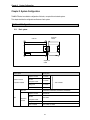
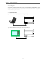
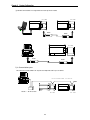
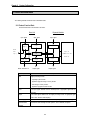
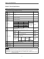
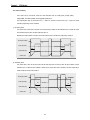
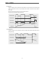
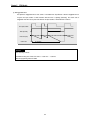
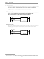
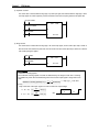
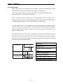
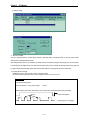
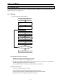
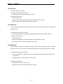
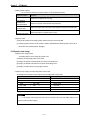
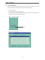
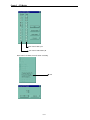
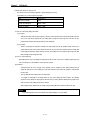
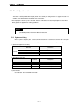
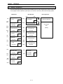
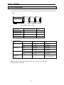
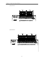
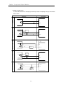
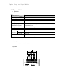
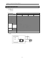
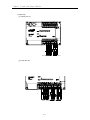
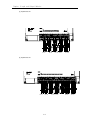
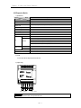
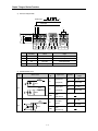
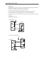
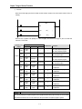

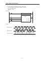
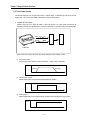
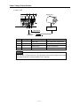
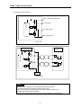
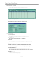
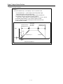
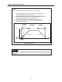
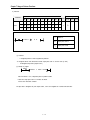
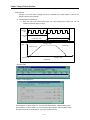
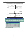
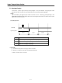
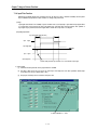
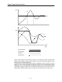
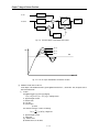
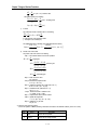
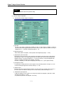
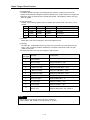
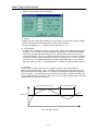
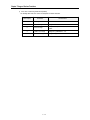
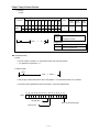
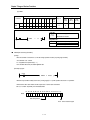
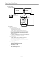
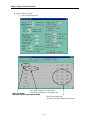
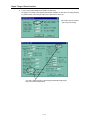
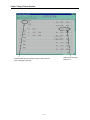
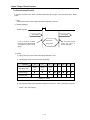
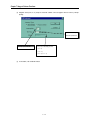
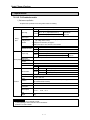

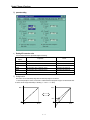
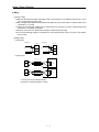
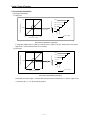

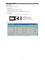
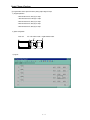
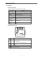
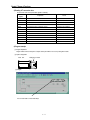
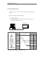
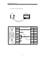
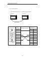
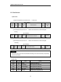
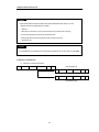
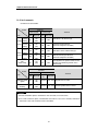
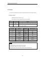
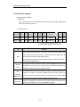
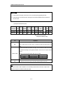
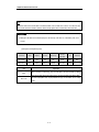


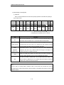
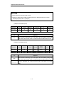
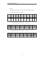
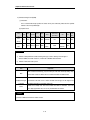
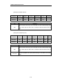
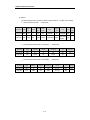

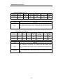
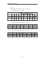
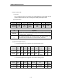
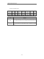
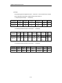
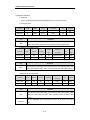
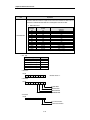
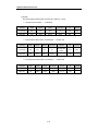
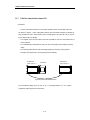
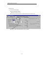
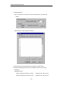
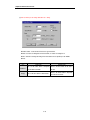
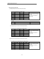
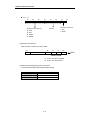
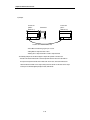
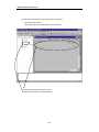
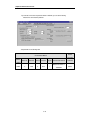
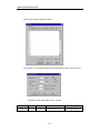
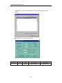


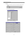
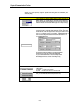

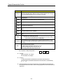

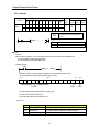
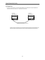
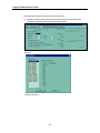
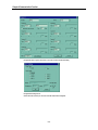
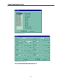
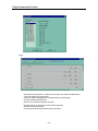
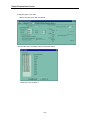
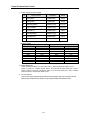
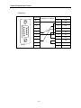
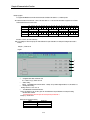
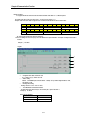
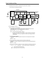
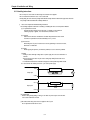
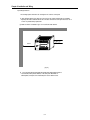
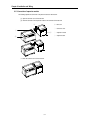
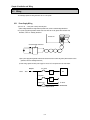
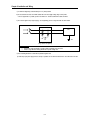
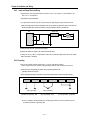
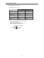


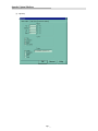
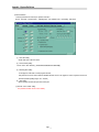
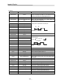


![[11] Chap.9 Installation and Wiring](http://vs1.manualzilla.com/store/data/005904878_1-e83dc78a4328ff11b1e565de6734c05d-150x150.png)