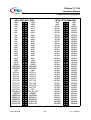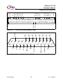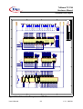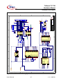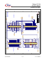
1
U s er’s Ma nual, V 3.1, Ja nuary 2005
TriBoard TC1796
H a r d w a r e M an u a l T C 1 7 9 6 . 3 0 0
M i c r o c o n t ro l le r s
N e v e r
s t o p
t h i n k i n g .
Edition 2005-01
Published by Infineon Technologies AG,
St.-Martin-Strasse 53,
D-81541 München, Germany
© Infineon Technologies AG 2005.
All Rights Reserved.
Attention please!
The information herein is given to describe certain components and shall not be considered as warranted
characteristics.
Terms of delivery and rights to technical change reserved.
We hereby disclaim any and all warranties, including but not limited to warranties of non-infringement, regarding
circuits, descriptions and charts stated herein.
Infineon Technologies is an approved CECC manufacturer.
Information
For further information on technology, delivery terms and conditions and prices please contact your nearest
Infineon Technologies Office in Germany or our Infineon Technologies Representatives worldwide (see address
list).
Warnings
Due to technical requirements components may contain dangerous substances. For information on the types in
question please contact your nearest Infineon Technologies Office.
Infineon Technologies Components may only be used in life-support devices or systems with the express written
approval of Infineon Technologies, if a failure of such components can reasonably be expected to cause the failure
of that life-support device or system, or to affect the safety or effectiveness of that device or system. Life support
devices or systems are intended to be implanted in the human body, or to support and/or maintain and sustain
and/or protect human life. If they fail, it is reasonable to assume that the health of the user or other persons may
be endangered.
U s er’s Ma nual, V 3.1, Ja nuary 2005
TriBoard TC1796
Hardware Manual TC1796.300
M i c r o c o n t ro l le r s
N e v e r
s t o p
t h i n k i n g .
TriBoard TC1796 Hardware Manual TC1796.100
Revision History:
2005-01
Previous Version:
-
Page
V 3.1
Subjects (major changes since last revision)
Controller Area Network (CAN): License of Robert Bosch GmbH
We Listen to Your Comments
Any information within this document that you feel is wrong, unclear or missing at all?
Your feedback will help us to continuously improve the quality of this document.
Please send your proposal (including a reference to this document) to:
[email protected]
TriBoard TC1796
Hardware Manual
Table of Contents
Page
1
Introduction . . . . . . . . . . . . . . . . . . . . . . . . . . . . . . . . . . . . . . . . . . . . . . 1-1
2
2.1
2.2
TriBoard Features . . . . . . . . . . . . . . . . . . . . . . . . . . . . . . . . . . . . . . . . . 2-1
Block Diagram . . . . . . . . . . . . . . . . . . . . . . . . . . . . . . . . . . . . . . . . . . . . . 2-2
Placement . . . . . . . . . . . . . . . . . . . . . . . . . . . . . . . . . . . . . . . . . . . . . . . . 2-3
3
3.1
3.2
3.3
Getting Started . . . . . . . . . . . . . . . . . . . . . . . . . . . . . . . . . . . . . . . . . . . .
Install the Tasking EDE Software. . . . . . . . . . . . . . . . . . . . . . . . . . . . . . .
Install the Driver for Debugging. . . . . . . . . . . . . . . . . . . . . . . . . . . . . . . .
Starting a New Tasking EDE >Project. . . . . . . . . . . . . . . . . . . . . . . . . . .
3-1
3-1
3-1
3-1
4
4.1
4.2
4.3
4.4
4.5
4.6
4.7
4.8
4.9
4.10
4.11
4.12
4.12.1
4.12.2
TriBoard Information . . . . . . . . . . . . . . . . . . . . . . . . . . . . . . . . . . . . . . .
Power Supply . . . . . . . . . . . . . . . . . . . . . . . . . . . . . . . . . . . . . . . . . . . . . .
Clock . . . . . . . . . . . . . . . . . . . . . . . . . . . . . . . . . . . . . . . . . . . . . . . . . . . .
Memory . . . . . . . . . . . . . . . . . . . . . . . . . . . . . . . . . . . . . . . . . . . . . . . . . .
FLASH . . . . . . . . . . . . . . . . . . . . . . . . . . . . . . . . . . . . . . . . . . . . . . . . . . .
SRAM . . . . . . . . . . . . . . . . . . . . . . . . . . . . . . . . . . . . . . . . . . . . . . . . . . .
Peripherals . . . . . . . . . . . . . . . . . . . . . . . . . . . . . . . . . . . . . . . . . . . . . . . .
ASC . . . . . . . . . . . . . . . . . . . . . . . . . . . . . . . . . . . . . . . . . . . . . . . . . . . . .
SSC . . . . . . . . . . . . . . . . . . . . . . . . . . . . . . . . . . . . . . . . . . . . . . . . . . . . .
MultiCAN . . . . . . . . . . . . . . . . . . . . . . . . . . . . . . . . . . . . . . . . . . . . . . . . .
Other peripherals . . . . . . . . . . . . . . . . . . . . . . . . . . . . . . . . . . . . . . . . . . .
Toggle LED . . . . . . . . . . . . . . . . . . . . . . . . . . . . . . . . . . . . . . . . . . . . . . .
Debug System . . . . . . . . . . . . . . . . . . . . . . . . . . . . . . . . . . . . . . . . . . . . .
OCDS . . . . . . . . . . . . . . . . . . . . . . . . . . . . . . . . . . . . . . . . . . . . . . . . .
On Board Wiggler . . . . . . . . . . . . . . . . . . . . . . . . . . . . . . . . . . . . . . . .
4-1
4-1
4-1
4-1
4-2
4-2
4-2
4-2
4-3
4-3
4-3
4-3
4-3
4-3
4-4
5
5.1
5.1.1
5.2
5.3
5.4
5.5
TriBoard Configuration . . . . . . . . . . . . . . . . . . . . . . . . . . . . . . . . . . . . .
HW Boot Configuration . . . . . . . . . . . . . . . . . . . . . . . . . . . . . . . . . . . . . .
TC1796 HW Boot Configuration . . . . . . . . . . . . . . . . . . . . . . . . . . . . .
SW Boot Configuration . . . . . . . . . . . . . . . . . . . . . . . . . . . . . . . . . . . . . .
Clock Selection . . . . . . . . . . . . . . . . . . . . . . . . . . . . . . . . . . . . . . . . . . . .
Jumper Settings. . . . . . . . . . . . . . . . . . . . . . . . . . . . . . . . . . . . . . . . . . . .
Optional Resistors . . . . . . . . . . . . . . . . . . . . . . . . . . . . . . . . . . . . . . . . . .
5-1
5-1
5-2
5-2
5-3
5-4
5-4
6
6.1
6.2
6.3
TriBoard Software . . . . . . . . . . . . . . . . . . . . . . . . . . . . . . . . . . . . . . . . .
Requirements . . . . . . . . . . . . . . . . . . . . . . . . . . . . . . . . . . . . . . . . . . . . .
Software Overview . . . . . . . . . . . . . . . . . . . . . . . . . . . . . . . . . . . . . . . . . .
Software Installation . . . . . . . . . . . . . . . . . . . . . . . . . . . . . . . . . . . . . . . .
6-1
6-1
6-1
6-1
7
Signal Description . . . . . . . . . . . . . . . . . . . . . . . . . . . . . . . . . . . . . . . . . 7-1
8
8.1
8.2
Connector Pin Assignment . . . . . . . . . . . . . . . . . . . . . . . . . . . . . . . . . . 8-1
TC1796 Connector / Top View . . . . . . . . . . . . . . . . . . . . . . . . . . . . . . . . 8-2
General Connector / Top View . . . . . . . . . . . . . . . . . . . . . . . . . . . . . . . . 8-4
User’s Manual
I-1
V 3.1, 2005-01
TriBoard TC1796
Hardware Manual
Table of Contents
Page
8.3
8.4
8.5
8.6
Power Connector Pinout . . . . . . . . . . . . . . . . . . . . . . . . . . . . . . . . . . . . .
RS232 Pinout . . . . . . . . . . . . . . . . . . . . . . . . . . . . . . . . . . . . . . . . . . . . . .
CAN Pinout . . . . . . . . . . . . . . . . . . . . . . . . . . . . . . . . . . . . . . . . . . . . . . .
OCDS Pinout . . . . . . . . . . . . . . . . . . . . . . . . . . . . . . . . . . . . . . . . . . . . . .
9
9.1
9.1.1
9.2
9.3
Schematic and Layout . . . . . . . . . . . . . . . . . . . . . . . . . . . . . . . . . . . . . . 9-1
Schematic . . . . . . . . . . . . . . . . . . . . . . . . . . . . . . . . . . . . . . . . . . . . . . . . 9-1
Know bugs and problems on the TriBoard TC1796.300 . . . . . . . . . . . 9-1
Layout . . . . . . . . . . . . . . . . . . . . . . . . . . . . . . . . . . . . . . . . . . . . . . . . . . 9-12
Layout with Dimensioning . . . . . . . . . . . . . . . . . . . . . . . . . . . . . . . . . . . 9-14
10
Keyword Index . . . . . . . . . . . . . . . . . . . . . . . . . . . . . . . . . . . . . . . . . Index-1
User’s Manual
I-2
8-6
8-6
8-8
8-8
V 3.1, 2005-01
TriBoard TC1796
Hardware Manual
List of Figures
Figure 2-1
Figure 2-2
Figure 4-1
Figure 5-1
Figure 8-1
Figure 8-2
Figure 8-3
Figure 8-4
Figure 8-5
Figure 8-6
Figure 8-7
Figure 8-8
Figure 8-9
Figure 8-10
Figure 8-11
Figure 9-1
Figure 9-2
Figure 9-3
Figure 9-4
Figure 9-5
Figure 9-6
Figure 9-7
Figure 9-8
Figure 9-9
Figure 9-10
Figure 9-11
Figure 9-12
Figure 9-13
Figure 9-14
User’s Manual
Page
TriBoard Block Schematic . . . . . . . . . . . . . . . . . . . . . . . . . . . . . . . . . 2-2
TriBoard-T1796.300 Placement . . . . . . . . . . . . . . . . . . . . . . . . . . . . . 2-3
Clock socket usage (XT301) . . . . . . . . . . . . . . . . . . . . . . . . . . . . . . . 4-1
HW Configuration DIP-Switch . . . . . . . . . . . . . . . . . . . . . . . . . . . . . . 5-1
Connector for TC1796 - Pinout (Part I, Top View) . . . . . . . . . . . . . . . 8-2
Connector for TC1796 - Pinout (Part II, Top View) . . . . . . . . . . . . . . 8-3
General Connector - Pinout (Part I, Top View) . . . . . . . . . . . . . . . . . 8-4
General Connector - Pinout (Part II, Top View) . . . . . . . . . . . . . . . . . 8-5
Power Connector Pinout . . . . . . . . . . . . . . . . . . . . . . . . . . . . . . . . . . 8-6
RS232-0 Pinout (DB9) . . . . . . . . . . . . . . . . . . . . . . . . . . . . . . . . . . . . 8-6
ASC1 Pinout (BERG10). . . . . . . . . . . . . . . . . . . . . . . . . . . . . . . . . . . 8-7
CAN Pinout (BERG10). . . . . . . . . . . . . . . . . . . . . . . . . . . . . . . . . . . . 8-8
3.3V OCDS1 Pinout (BERG16) . . . . . . . . . . . . . . . . . . . . . . . . . . . . . 8-8
3.3V OCDS2 Pinout (SAMTEC QSH) . . . . . . . . . . . . . . . . . . . . . . . . 8-9
On Board Wiggler Pinout (DB25) . . . . . . . . . . . . . . . . . . . . . . . . . . . . 8-9
Schematic - Project . . . . . . . . . . . . . . . . . . . . . . . . . . . . . . . . . . . . . . 9-2
Schematic - Bussystem and SRAM . . . . . . . . . . . . . . . . . . . . . . . . . . 9-3
Schematic - On Board Flash Memory . . . . . . . . . . . . . . . . . . . . . . . . 9-4
Schematic - Clock, OCDS and Config . . . . . . . . . . . . . . . . . . . . . . . . 9-5
Schematic - Peripherals. . . . . . . . . . . . . . . . . . . . . . . . . . . . . . . . . . . 9-6
Schematic - Debug System . . . . . . . . . . . . . . . . . . . . . . . . . . . . . . . . 9-7
Schematic - ADC and GPTA . . . . . . . . . . . . . . . . . . . . . . . . . . . . . . . 9-8
Schematic - Power Supply . . . . . . . . . . . . . . . . . . . . . . . . . . . . . . . . . 9-9
Schematic - Connectors (Plug) . . . . . . . . . . . . . . . . . . . . . . . . . . . . 9-10
Schematic - Connectors (Socket) . . . . . . . . . . . . . . . . . . . . . . . . . . 9-11
Component Plot Top Layer . . . . . . . . . . . . . . . . . . . . . . . . . . . . . . . 9-12
Component Plot Bottom Layer. . . . . . . . . . . . . . . . . . . . . . . . . . . . . 9-13
Dimensioning (mil) . . . . . . . . . . . . . . . . . . . . . . . . . . . . . . . . . . . . . . 9-14
Dimensioning (mm) . . . . . . . . . . . . . . . . . . . . . . . . . . . . . . . . . . . . . 9-15
II-1
V 3.1, 2005-01
TriBoard TC1796
Hardware Manual
List of Figures
User’s Manual
Page
II-2
V 3.1, 2005-01
TriBoard TC1796
Hardware Manual
List of Tables
Table 5-1
Table 5-2
Table 5-3
Table 5-4
Table 5-5
Table 5-6
Table 5-7
Table 5-8
Table 5-9
Table 5-10
Table 7-1
Table 7-2
Table 7-3
Table 7-4
Table 7-5
Table 7-6
Table 7-7
Table 7-8
User’s Manual
Page
HW Boot Configuration for TC1796 . . . . . . . . . . . . . . . . . . . . . . . . . .
Jumper for ASC0 . . . . . . . . . . . . . . . . . . . . . . . . . . . . . . . . . . . . . . . .
Jumper for ASC1 . . . . . . . . . . . . . . . . . . . . . . . . . . . . . . . . . . . . . . . .
Jumper for On Board Wiggler . . . . . . . . . . . . . . . . . . . . . . . . . . . . . .
Resistors for XTAL1 Operation . . . . . . . . . . . . . . . . . . . . . . . . . . . . .
Resistors for flash AM29BL162C . . . . . . . . . . . . . . . . . . . . . . . . . . . .
Resistors for 32 bit flash . . . . . . . . . . . . . . . . . . . . . . . . . . . . . . . . . .
Resistors for other 16 bit flash . . . . . . . . . . . . . . . . . . . . . . . . . . . . . .
Resistors for asynchronous SRAM . . . . . . . . . . . . . . . . . . . . . . . . . .
Resistors for synchronous SRAM . . . . . . . . . . . . . . . . . . . . . . . . . . .
Power Signals . . . . . . . . . . . . . . . . . . . . . . . . . . . . . . . . . . . . . . . . . .
Reset Signals. . . . . . . . . . . . . . . . . . . . . . . . . . . . . . . . . . . . . . . . . . .
Interrupt Signals. . . . . . . . . . . . . . . . . . . . . . . . . . . . . . . . . . . . . . . . .
Clock Signals . . . . . . . . . . . . . . . . . . . . . . . . . . . . . . . . . . . . . . . . . . .
BUS Signals. . . . . . . . . . . . . . . . . . . . . . . . . . . . . . . . . . . . . . . . . . . .
BUS Control Signals . . . . . . . . . . . . . . . . . . . . . . . . . . . . . . . . . . . . .
Debug Signals . . . . . . . . . . . . . . . . . . . . . . . . . . . . . . . . . . . . . . . . . .
Peripheral Signals . . . . . . . . . . . . . . . . . . . . . . . . . . . . . . . . . . . . . . .
III-3
5-2
5-4
5-4
5-4
5-4
5-4
5-5
5-5
5-5
5-5
7-1
7-1
7-2
7-2
7-2
7-2
7-3
7-3
V 3.1, 2005-01
TriBoard TC1796
Hardware Manual
List of Tables
User’s Manual
Page
III-4
V 3.1, 2005-01
TriBoard TC1796
Hardware Manual
Introduction
1
Introduction
We congratulate you on your purchase of the TriCore Evaluation Board. This kit is a
versatile tool, providing quick access to the capabilities of TriCore's powerful
architecture.
Applications can be developed easily. The Evaluation Board is equipped with a variety
of memories and peripherals for connection to the environment. There is also an
interface for the On Chip Debugging Features (OCDS1 and OCDS2). The kit also
includes several sets of development tools, which are stored on the included Evaluation
Board CD-ROM.
The Evaluation Board allows easily the development of TriCore applications with the
corresponding tools.
Subsequently, the applications can be downloaded and can be tested with the powerful
debugger software.
This TriBoard Hardware Manual familiarizes you with the TriCore Evaluation Board and
guides you through the initial setup of the TriBoard and the installation of the
development software tool chain.
User’s Manual
1-1
V 3.1, 2005-01
TriBoard TC1796
Hardware Manual
Introduction
User’s Manual
1-2
V 3.1, 2005-01
TriBoard TC1796
Hardware Manual
TriBoard Features
2
TriBoard Features
• CPU:
• MEMORY:
• CLOCK:
• INTERFACE:
• POWER:
• DIMENSION:
User’s Manual
- TC1796 (TriCore)
- Burst FLASH up to 16 MBytes (default:4 MBytes)
- asynchronous SRAM up to 1MBytes (default)
- optional synchronous SRAM up to 8 MBytes
- Crystal 20MHz (default), Oscillator or External Clock
- DB9 for RS232-0
- BERG10 for RS232-1
- two BERG10 for CAN-0/1 with Transceiver
- BERG16 for OCDS1
- SAMTEC QSH-030-01-F-D-A for OCDS2
- DB25 On Board Wiggler for OCDS1
- four 80-pin connectors (male) with all I/O signals
- four 80-pin connectors (female) with all I/O signals
- 5,5V to 60V
- generated internally 3.3V, 1.5V (optional 2.5V for Bussystem)
- generated internally 5V for OnBoard Wiggler and CAN
Transceiver
- Power On Reset circuit
- 100mm x 160mm (EURO-Board)
2-1
V 3.1, 2005-01
TriBoard TC1796
Hardware Manual
TriBoard Features
2.1
Block Diagram
XTAL
CAN0
PLL
TxCAN0
RxCAN0
Transceiver
CAN1
TxCAN1
RxCAN1
TC1796A
ASC0
BUS
TxD0
RxD0
Transceiver
TxD1
TriCore
CPU
ADDRESS and DATA BUS
BUS
/CS0 or /CS1
BUS
RxD1
ASC1
User’s Manual
SRAM
32 Bit
O CDS1
OCDS2
W iggler
OCDS1
/CS0 or /CS1
W iggler
Figure 2-1
Burst
FLASH
32 Bit
TriBoard Block Schematic
2-2
V 3.1, 2005-01
TriBoard TC1796
Hardware Manual
TriBoard Features
Placement
X804
1
XT301
Clock
CAN1 CAN0
5V
3V3
1
OCDS2
JP501
1
1
1V5
2V5
1
S301
JP401
1
8
Asynchr.
SRAM
1
JP402
1
X801 BUS EXPANSION
GPTA / MLI
Asynchr.
SRAM
1
RS232-0
RS232-1
2.2
RESET
Synchr.
SRAM
TC1796A
ED CON.
1
TOGGLE
Burst
FLASH
32Bit
1
OCDS1
Wiggler
A1
Reset
Power
X803
Burst FLASH
16Bit
ADC
X802
1
Figure 2-2
User’s Manual
Burst FLASH
16Bit
PERIPHERALS
1
TriBoard-T1796.300 Placement
2-3
V 3.1, 2005-01
TriBoard TC1796
Hardware Manual
TriBoard Features
User’s Manual
2-4
V 3.1, 2005-01
TriBoard TC1796
Hardware Manual
Getting Started
3
Getting Started
This section provides a basic understanding of how to upload a program to the TriBoard
and run the debugger. In this example the software from Tasking Version 1.5r1 or higher
will be used to explain the first steps. The needed driver for debugging runs only with
WindowsNT 4.00 and Windows 2000. To install the driver you need “Power User” or
“Administrator” rights, because editing of the registry is required.
3.1
Install the Tasking EDE Software.
A demo of the Tasking Software can be found in the WWW under the URL:
http://www.tasking.com
Insert your Tasking CD on your CD drive and start “Setup.exe”, if the program is not
executed automatic then change to your CD drive and start “Setup.exe” manually or
download a demo from the Tasking website and start “Setup.exe” and follow the
instructions.
3.2
Install the Driver for Debugging.
The Driver is located in the “\Tools\Driver\” directory. Start “Reg_JTAGdrv.exe”. Now
copy all subdirectories from “\Tools\Driver\Tasking\” to your Tasking folder. The default
location of the Tasking files is “C:\CTri\”. All files with the same name should be
overwritten.
The file “ReadMe.txt” in this directory contains some additional informations. The driver
works with only with Windows NT4.00 and Windows 2000.
3.3
Starting a New Tasking EDE >Project.
This section will be filled at the next release of TriBoard Manual for TC1796.
User’s Manual
3-1
V 3.1, 2005-01
TriBoard TC1796
Hardware Manual
Getting Started
User’s Manual
3-2
V 3.1, 2005-01
TriBoard TC1796
Hardware Manual
TriBoard Information
4
TriBoard Information
4.1
Power Supply
The Board has to be connected to a 5,5V to 60V DC power supply. The TriBoard
generates internally 3.3V, 1.5V (optional 2.5V for the bussystem) and 5V. The power
consumption is not specified yet but a supply with 7V and 500mA should be sufficient.
The pinout for the supply connector is shown in Figure 8-5. There can be used any
standard power pack with a connector where the positive line is surrounded by the
ground line.
Applying a stable supply voltage causes the power on reset after a short period. The four
LED's (5V, 3.3V, 2.5V, 1.5V) indicate the status of the on board generated voltage (if the
LEDs are assembled).
A manual reset is executed by pressing the reset button.
4.2
Clock
There are three possibilities to apply the CPU clock.
•
•
•
•
Large oscillator circuit (DIP14)
Small oscillator circuit (DIP8)
Crystal oscillator (default)
External clock generator
The crystal oscillator and the oscillator circuit use the socket XT301. It's possible to apply
a 14pol DIP oscillator package or an 8pol DIP oscillator package.
OSCILLATOR
DIP14
XTAL
OSCILLATOR
DIP8
Figure 4-1
4.3
GND
External
Clock Input
Clock socket usage (XT301)
Memory
The TriBoard supports the following memory configurations:
• up to 8 MBytes external Burst Flash (2x16Bit) or
• 4 MBytes external Burst Flash (1x32Bit)
• 1 MBytes external asynchronous SRAM (2x16Bit) or
User’s Manual
4-1
V 3.1, 2005-01
TriBoard TC1796
Hardware Manual
TriBoard Information
• up to 8 MBytes external synchronous SRAM (1x32Bit)
For the OnBoardMemory are reserved chip select 0 and 1. Therefore only two parts, e.g.
2x16Bit Flash and 2x16Bit asynchronous SRAM, should be assembled and can be used
at the same time. Chip Select 2 and 3 are not used on the board and can be used
externally.
The Board supports programming though the JTAG port (OCDS1).
4.4
FLASH
The flash uses 32 Data Bits (AD0...AD31) and 20, 21 or 22 Address Bits (A2...A21,A22
or A23). It’s accessed via /CS0 or /CS1. Each type of flash has its own resistor to
connect to /CS0 or /CS1. For connect the different flash see Chapter 5.5.
4.5
SRAM
The SRAM uses 32 Data Bits (AD0...AD31) and up to 22 Address Bits (A2...A22).
It’s accessed via /CS0 or /CS1. Each type of SRAM has its own resistor to connect to /
CS0 or /CS1. For connect the different SRAM see Chapter 5.5.
4.6
•
•
•
•
•
•
•
•
•
Peripherals
The available peripherals on the TC1796 are
System Timer
General Purpose Timer Array V4 (GPTA0, GPTA1 and LTCA2)
Asynchronous Serial Interface (ASC0 and ASC1)
Synchronous Serial Interface (SSC0 and SSC1)
MultiCAN (CAN0, CAN1, CAN2 and CAN3)
Micro Second Bus Interface (MSC0 and MSC1)
Micro Link Serial Bus Interface (MLI0 and MLI1)
Analog Digital Converter (ADC0,ADC1 and FADC) with 44 analog inputs
4.7
ASC
There are two ASC interfaces possible. ASC0 is connected to the DB9 socket and ASC1
is connected to the BERG10 plug. ASC0 and ASC1 are driven via the RS232
Transceiver MAX3225. The DB9 socket can be connected to the serial port of a PC with
a 1 to 1 RS232 cable.
To use the interfaces ASC0 and ASC1 via the plug X802 (without Transceiver) jumper
JP401 (see Table 5-2 "Jumper for ASC0" on Page 5-4) and JP402 (see Table 5-3
"Jumper for ASC1" on Page 5-4) have to be changed (see Figure 9-11).
User’s Manual
4-2
V 3.1, 2005-01
TriBoard TC1796
Hardware Manual
TriBoard Information
4.8
SSC
On the TC1796A there are two synchronous serial interfaces available but there is no
special plug on board. To connect peripherals to SSC’s the connector X802
(Peripherals) can be used.
The SSC0 of the TC1796A is connected to a serial EEPROM with a size of 128K (16.384
x 8). As chip select for this EEPROM is used the line SLSO0. To disable the EEPROM
remove resistor R406.
4.9
MultiCAN
On the board are two CAN transceiver connected to the MultiCAN on TC1796 node 0
and 1. The transceivers are connected to two BERG10 plug. For the pinout of BERG10
plug see Figure 8-8.
The other two nodes (CAN2 and CAN3) can be use via plug X802. To use the CAN0 and
CAN1 interfaces via the plug X802 (without Transceiver) remove resistors R409 and
R410 and assemble R404 and R405 with a 0R resistor.
4.10
Other peripherals
For all other peripherals there are no special plugs on the board. The peripheral signals
are available on the different connectors. See “Connector Pin Assignment” on
Page 8-1.
Note: - SLSO0 is used as chip select for the serial eeprom on board.
4.11
Toggle LED
Port 1 pin 15 is connected to a single LED (D401) and can be controlled by Software.
This status LED is low active.
4.12
Debug System
4.12.1
OCDS
The OCDS1 signals are connected to the BERG16 plug (X501). They work with the port
supply of 3.3V.
The OCDS2 signals are connected to the SAMTEC HighSpeed plug (X502). They also
work with the port supply of 3.3V.
The clock signal for OCDS1 and OCDS2 is always TRCLK (this clock must be enabled
by software for using this clock).
User’s Manual
4-3
V 3.1, 2005-01
TriBoard TC1796
Hardware Manual
TriBoard Information
4.12.2
On Board Wiggler
The On Board Wiggler is used to connect a PC to the TriBoard OCDS1 via the 5V parallel
port.
The Wiggler can be enabled or disabled by setting the jumper JP501 (see Table 5-4
"Jumper for On Board Wiggler" on Page 5-4 and Figure 9-11).
User’s Manual
4-4
V 3.1, 2005-01
TriBoard TC1796
Hardware Manual
TriBoard Configuration
TriBoard Configuration
5.1
HW Boot Configuration
HIGH
1
Figure 5-1
se
d
O
no
tu
TM
/T
ES
R
ST
TS
T
BY
PA
SS
C
FG
3
H
W
C
FG
2
W
H
W
H
LOW
H
W
C
FG
0
C
FG
1
D
E
5
on
2
3
4
5
6
7
8
HW Configuration DIP-Switch
The picture above shows the definition of the boot HW configuration switch. The
meaning of the switches will be described in the following table (Table 5-1).
Note: The ON position of the switch is equal to a logical LOW at the dedicated pin.
User’s Manual
5-1
V 3.1, 2005-01
TriBoard TC1796
Hardware Manual
TriBoard Configuration
5.1.1
TC1796 HW Boot Configuration
Table 5-1
HW Boot Configuration for TC1796
Note: The shadowed line indicates the default setting.
Note: ’x’ represents the don’t care state.
Note: The signal /BRK_IN will be set by the Debugger via OCDS-Interface.
/BRK_IN
HWCFG[3...0] Type of Boot
PC Start value
1
0000
Serial boot from ASC to PMI
scratchpad, run loaded program
0xD4000000
1
0001
Serial boot from CAN to PMI
scratchpad, run loaded program
0xD4000000
1
0010
Start from internal flash
0xA0000000
1
0011
Alternate Bootmode from internal flash from Header or
0xD4000000
1
0100
External memory, EBU as master
0xA1000000
1
0101
Alternate Bootmode from External
memory, EBU as master
from Header or
0xD4000000
1
0110
External memory, EBU as slave
0xA1000000
1
0111
Alternate Bootmode from External
memory, EBU as slave
from Header or
0xD4000000
1
1XXX
reserved; don’t use this combination
-
0
1000
go to external emulator space
0xDE000000
0
0000
put chip in tristate (deep sleep)
-
0
all others
reserved; don’t use this combination
-
5.2
SW Boot Configuration
The TC1796 has 16 inputs (Port 0) which are latched with the /HRST signal. This latched
value can be used as SW configuration. On the Bottomside (see Figure 9-12) from the
TriBoard exist two Dipswitches which can be used for SW configuration. The
Dipswitches connect the port inputs to ground via 1k resistor. The port has internal
pullups. If the Dipswitch is closed the the corresponding bit is low otherwise high.
The following inputs are used by the bootrom software and should be used carefully:
P0.0, P0.1 and P0.2 are used by the Alternate Bootmode for selecting the
Bootstraploader in case of not usable Alternate Boot.
User’s Manual
5-2
V 3.1, 2005-01
TriBoard TC1796
Hardware Manual
TriBoard Configuration
P0.4 is used to disable flash accesses in the bootrom. In case of not functional flash of
device make sure that switch 5 of S401 is ON. Normally this switch should be OFF. Is
this switch is ON then the internal flash is not usable.
Refer to Users Manual TC1796 for more information.
All other pins can be used by your own software.
5.3
Clock Selection
The resulting CPU clock is:
•
N
f CPUCLK = -------- ⋅ f OSC
PK
•
f CPUCLK = f OSC
without Bypass (switch is ON)
with Bypass (switch is OFF)
Note: The factors K, P and N are controlled via bitfields in register PLL_CLC located in
the SCU.
The resulting system clock is:
•
f CPUCLK
f SYSTEMCLK = -------------------2
if SYSFS cleared (default after reset)
•
f SYSTEMCLK = f CPUCLK
if SYSFS is set
Note: The bit SYSFS is controlled via bit 2 in register PLL_CLC located in the SCU.
User’s Manual
5-3
V 3.1, 2005-01
TriBoard TC1796
Hardware Manual
TriBoard Configuration
5.4
Jumper Settings.
Table 5-2
Jumper for ASC0
Note: The shadowed line indicates the default setting
Setting
ASC0 Configuration
1-2
Transceiver --> CPU
2-3
ext. RxD --> CPU
Table 5-3
Jumper for ASC1
Note: The shadowed line indicates the default setting
Setting
ASC1 Configuration
1-2
Transceiver --> CPU
2-3
ext. RxD --> CPU
Table 5-4
Jumper for On Board Wiggler
Note: The shadowed line indicates the default setting
Setting
On Board Wiggler
1-2
Enable On Board Wiggler
2-3
Disable On Board Wiggler
5.5
Optional Resistors
Table 5-5
Resistors for XTAL1 Operation
R314
use XT301 (default: short)
R315
Rserial (default: short)
R316
Rparallel (default: open)
Table 5-6
Resistors for flash AM29BL162C
R212
use /CS0 (default: short)
R213
use /CS1 (default: open)
R214
pullup on chip select the device (default: open)
User’s Manual
5-4
V 3.1, 2005-01
TriBoard TC1796
Hardware Manual
TriBoard Configuration
Table 5-7
Resistors for 32 bit flash
R218
use /CS0 (default: open)
R219
use /CS1 (default: open)
R220
pullup on chip select the device (default: open)
Table 5-8
Resistors for other 16 bit flash
R215
use /CS0 (default: open)
R216
use /CS1 (default: open)
R217
pullup on chip select the device (default: open)
Table 5-9
Resistors for asynchronous SRAM
R122
use /CS0 (default: open)
R121
use /CS1 (default: short)
R123
pullup on chip select the device (default: open)
Table 5-10
Resistors for synchronous SRAM
R125
use /CS0 (default: open)
R124
use /CS1 (default: open)
R126
pullup on chip select the device (default: open)
User’s Manual
5-5
V 3.1, 2005-01
TriBoard TC1796
Hardware Manual
TriBoard Configuration
User’s Manual
5-6
V 3.1, 2005-01
TriBoard TC1796
Hardware Manual
TriBoard Software
6
TriBoard Software
6.1
Requirements
To install the software from your TriBoard CD you need a PC with Windows95/98/ME,
WindowsNT4.0 or Windows 2000.
6.2
Software Overview
The CD does not contain any tool. For the availablity for Demo Versions of the different
Tools, please contact the toolvendor directly (e.g. Tasking, Hitex, Lauterbach,
GreenHills, HighTec...). To install tools for compiling and debugging use seperat CD’s
from Toolvendors. There are also some application notes and software examples. The
directory “Schematics” contains libraries and some examples of extension boards in the
Protel file format. The data sheets of all used parts can be found in the
“TriBoard_Components” directory. The manuals for the microcontrollers and the
TriBoard are located in the “Manual” folder. Some useful tools like Acrobat Reader are
stored in the “Utilities” directory.
The current Errata Sheet can be found in the directory “Errata Sheet”. To make sure you
have always the most recent one, please contact your local FAE.
Note: For more details see the file ReadMe.txt.
6.3
Software Installation
To install tools for the TriCore insert the CD from the Toolvendor and start the file
“setup.exe” if the CD is not automatically started. Follow the instructions of the
installationprogram.
User’s Manual
6-1
V 3.1, 2005-01
TriBoard TC1796
Hardware Manual
TriBoard Software
User’s Manual
6-2
V 3.1, 2005-01
TriBoard TC1796
Hardware Manual
Signal Description
7
Signal Description
For more information about the signals please see the user manuals from TC1796.
Table 7-1
Power Signals
Short Name
Description
VCC_IN
Supply Input (5,5V...60V)
GND
Ground
VDD
Core Supply Voltage (1.5V)
VDDP
Port Supply Voltage (3.3V)
VDDEBU
External Bus Supply Voltage (2.5V or 3.3V)
VDDFL3
Flash Supply Voltage (3.3V)
VDDSBRAM
SRAM standby Supply Voltage (1.5V)
VDDOSC
Main Oscillator Supply Voltage (1.5V)
VDDOSC3
Main Oscillator Supply Voltage (3.3V)
VSSOSC
Main Oscillator Ground
VSSM
ADC0/1 Analog Part Ground
VDDM
ADC0/1 Analog Part Supply Voltage
VSSMF
FADC Analog Part Ground
VDDMF
FADC Analog Part Supply Voltage
VAGND0
ADC0 Reference Ground
VAREF0
ADC0 Reference Voltage
VAGND1
ADC1 Reference Ground
VAREF1
ADC0 Reference Voltage
VFAGND
FADC Reference Ground
VFAREF
FADC Reference Voltage
Table 7-2
Reset Signals
Short Name
Description
/PORST
External Power On Reset
/HDRST
Hardware Reset
TSTRES
Test Reset
User’s Manual
7-1
V 3.1, 2005-01
TriBoard TC1796
Hardware Manual
Signal Description
Table 7-3
Interrupt Signals
Short Name
Description
/NMI
Non Maskable Interrupt
REQ[0...7]
External Trigger Input 0...7
Table 7-4
Clock Signals
Short Name
Description
XTAL1
Crystal Oscillator Input
XTAL2
Crystal Oscillator Output
BFCLKO
Burst Mode Flash Clock Output
BFCLKI
Burst Mode Flash Clock Input
Table 7-5
BUS Signals
Short Name
Description
D[0...31]
Data Bus
A[0...23]
Address Bus
Table 7-6
BUS Control Signals
Short Name
Description
/CS[0...3]
Chip Selects
/CSCOMB
Combined Chip Select Output
/BC[0...3]
Byte Controls
/RD
Read
/WR
Write
MR/W
Motorola-style Read/Write
/BAA
Burst address advance output
/ADV
Address Valid
/BREQ
Bus Request Output
/HOLD
Hold Request Input
/HLDA
Hold Acknowledge
/WAIT
Wait Input
User’s Manual
7-2
V 3.1, 2005-01
TriBoard TC1796
Hardware Manual
Signal Description
Table 7-7
Debug Signals
Short Name
Description
/TRST
Test Reset
TCLK
Test Clock
TMS
Test Mode Select
TDI
Test Data Input
TDO
Test Data Output
TRCLK
Trace Clock for OCDS Level 2
TESTMODE
Test Mode Select Input
/BRK_IN
TriCore Breakpoint Input
BYPASS
Bypass PLL
/BRK_OUT
TriCore Breakpoint Output
BRKPT[0...2]
TriCore Breakpoint (TR5..7)
STATUS[0...4]
TriCore Status (TR0..4)
IND_PC[0...7]
TriCore Indirect Program Counter (TR8..15)
Table 7-8
Peripheral Signals
Short Name
Description
RXD0
Receive Data ASC0
RXD0_EXT
Receive Data ASC0 (see Table 5.3)
TXD1
Transmit Data ASC1
RXD1_EXT
Receive Data ASC1 (see Table 5.3)
SCLK0
Clock Line SSC0
MRST0
Master Receive / Slave Transmit SSC0
MTSR0
Master Transmit / Slave Receive SSC0
SLSI0
Slave Select Input SSC0
SLSO0
Slave Select Output 0 (SSC0)
SLSO1
Slave Select Output 1 (SSC0)
SCLK1
Clock Line SSC1
MRST1
Master Receive / Slave Transmit SSC1
MTSR1
Master Transmit / Slave Receive SSC1
SLSI1
Slave Select Input SSC1
SLSO[2..7]
Slave Select Output 2..7
User’s Manual
7-3
V 3.1, 2005-01
TriBoard TC1796
Hardware Manual
Signal Description
Table 7-8
Peripheral Signals
TXCAN0
CAN Transmitter Output 0
RXCAN0
CAN Receiver Input 0
TXCAN1
CAN Transmitter Output 1
RXCAN1
CAN Receiver Input 1
TXCAN2
CAN Transmitter Output 2
RXCAN2
CAN Receiver Input 2
TXCAN3
CAN Transmitter Output 3
RXCAN3
CAN Receiver Input 3
GPTUA [0...55]
General Purpose Timer Array
P0 [0...15]
General Purpose I/O Port 0 (SWOPT)
P1[12...15]
General Purpose I/O Port 1.12...1.15
AN[0...43]
Analog Inputs
AD0EMUX[0...1]
ADC0 External Multiplexer Control
AD1EMUX[0...1]
ADC1 External Multiplexer Control
FCLP0A
MSC0 differential driver clock output positive A
FCLN0
MSC0 differential driver clock output negative
SOP0A
MSC0 differential driver serial data output positive A
SON0
MSC0 differential driver serial data output negative
EN00
MSC0 device select output 0
SDI0
MSC0 serial data input
FCLP1A
MSC1 differential driver clock output positive A
FCLN1
MSC1 differential driver clock output negative
SOP1A
MSC1 differential driver serial data output positive A
SON1
MSC1 differential driver serial data output negative
EN10
MSC1 device select output 0
SDI1
MSC1 serial data input
RCLK0
MLI0 receive channel clock
RREADY0
MLI0 receive channel ready output
RVALID0
MLI0 receive channel valid input
RDATA0
MLI0 receive channel data input
TCLK0
MLI0 transmit channel clock
User’s Manual
7-4
V 3.1, 2005-01
TriBoard TC1796
Hardware Manual
Signal Description
Table 7-8
Peripheral Signals
TREADY0
MLI0 transmit channel ready input
TVALID0
MLI0 transmit channel valid output
TDATA0
MLI0 transmit channel data output
P10[0...3]
General Purpose I/O Port 10 (used as HWCFG)
User’s Manual
7-5
V 3.1, 2005-01
TriBoard TC1796
Hardware Manual
Signal Description
User’s Manual
7-6
V 3.1, 2005-01
TriBoard TC1796
Hardware Manual
Connector Pin Assignment
8
Connector Pin Assignment
The TriBoard will be shipped with four male (plug) connectors on top layer and four
female (socket) connectors on bottom layer. The default connectors are 80-pol. Board to
Board connectors from Samtec:
http://www.samtec.com
Plug:Socket:
FTSH-140-02-L-DV-ES-AFLE-140-01-G-DV-A
Alternative there can be used the Board to Board System from Robinson Nugent:
http://www.robinsonnugent.com
Plug:Socket:
P50L-80P-AS-TGFP50L-80S-AS-TGF
User’s Manual
8-1
V 3.1, 2005-01
TriBoard TC1796
Hardware Manual
Connector Pin Assignment
8.1
TC1796 Connector / Top View
BUS EXPANSION (X801,X901)
GND
GND
D0
D1
D2
D3
D4
D5
D6
D7
D8
D9
D10
D11
D12
D13
D14
D15
D16
D17
D18
D19
D20
D21
D22
D23
D24
D25
D26
D27
D28
D29
D30
D31
/RD
/WR
MR/W
/HLDA
/HOLD
Figure 8-1
User’s Manual
1 2
3 4
5 6
7 8
9 10
11 12
13 14
15 16
17 18
19 20
21 22
23 24
25 26
27 28
29 30
31 32
33 34
35 36
37 38
39 40
41 42
43 44
45 46
47 48
49 50
51 52
53 54
55 56
57 58
59 60
61 62
63 64
65 66
67 68
69 70
71 72
73 74
75 76
77 78
79 80
PERIPHERALS (X802,X902)
GND
GND
A0
A1
A2
A3
A4
A5
A6
A7
A8
A9
A10
A11
A12
A13
A14
A15
A16
A17
A18
A19
A20
A21
A22
A23
GND
GND
VCC_IN
VCC_IN
/ADV
BFCLKO
P0.5
/NMI
DSQ0
GND
P0.6
P0.7
EN00 / P5.4
SDI0 / P5.5
FCLP0A
FCLN0
SOP0A
SON0
RXCAN3 / P6.14
SLSI0
SLSO0
SLSO2 / P2.2
SLSO4 / P2.4
SLSO6 / P2.6
GND
XTAL1
XTAL2
RXD0_EXT / P5.0
TXD0 / P5.1
RXCAN0 / P6.8
TXCAN0 / P6.9
SCLK0
MTSR0
MRST0
RXCAN2 / P6.12
REQ0 / P1.0
REQ2 / P1.2
VDDSBRAM
3V3
3V3
/CS2
/CS1
/CS0
/BC3
/BC2
/BC1
/BC0
/CSCOMB
/WAIT
/BREQ
/CS3
1 2
3 4
5 6
7 8
9 10
11 12
13 14
15 16
17 18
19 20
21 22
23 24
25 26
27 28
29 30
31 32
33 34
35 36
37 38
39 40
41 42
43 44
45 46
47 48
49 50
51 52
53 54
55 56
57 58
59 60
61 62
63 64
65 66
67 68
69 70
71 72
73 74
75 76
77 78
79 80
GND
GND
VCC_IN
VCC_IN
/BAA
BCK
/BCK
/HDRST
DSQ1
GND
/PORST
P0.8
EN10 / P5.6
SDI1 / P5.7
FCLP1A
FCLN1
SOP1A
SON1
TXCAN3 / P6.15
SLSI1
SLSO1
SLSO3 / P2.3
SLSO5 / P2.5
SLSO7 / P2.7
GND
SYSCLK / P1.12
BFCLKI
RXD1_EXT / P5.2
TXD1 / P5.3
RXCAN1 / P6.10
TXCAN1 / P6.11
SCLK1 / P6.6
MTSR1 / P6.4
MRST1 / P6.5
TXCAN2 / P6.13
REQ1 / P1.1
REQ3 / P1.3
GND
VDDE
VDDE
Connector for TC1796 - Pinout (Part I, Top View)
8-2
V 3.1, 2005-01
TriBoard TC1796
Hardware Manual
Connector Pin Assignment
ADC (X803, X903)
VSSA
VSSA
AN0
AN1
AN2
AN3
AN4
AN5
AN6
AN7
AN8
AN9
AN10
AN11
AN12
AN13
AN14
AN15
VSSA
VDDM
VSSFAREF
VSSAREF0
VDDAREF0
VSSA
AN32
AN33
AN34
AN35
AN36
AN37
VSSA
P0.8
P0.10
P0.12
3V3
AD0EMUX0 / P7.2
AD0EMUX1 / P7.3
REQ5 / P7.1
P0.15
REQ7 / P7.5
Figure 8-2
User’s Manual
GPTA / MLI (X804,X904)
1 2
VSSA
3 4
VSSA
5 6
AN16
7 8
AN17
9 10
AN18
11 12
AN19
13 14
AN20
15 16
AN21
17 18
AN22
19 20
AN23
21 22
AN24
23 24
AN25
25 26
AN26
27 28
AN27
29 30
AN28
31 32
AN29
33 34
AN30
35 36
AN31
37 38
VSSA
39 40
VDDMF
41 42 VDDFAREF
43 44
VSSAREF1
45 46
VDDAREF1
47 48
VSSA
49 50
AN38
51 52
AN39
53 54
AN40
55 56
AN41
57 58
AN42
59 60
AN43
61 62
VSSA
63 64
P0.9
65 66
P0.11
67 68
P0.13
69 70
VDDE
71 72 AD1EMUX0 / P7.6
73 74 AD1EMUX1 / P7.7
75 76
P0.14
77 78 REQ4 / P7.0
79 80 REQ6 / P7.4
GND
GND
GPTA0 / P2.8
GPTA1 / P2.9
GPTA2 / P2.10
GPTA3 / P2.11
GPTA4 / P2.12
GPTA5 / P2.13
GPTA6 / P2.14
GPTA7 / P2.15
GPTA8 / P3.0
GPTA9 / P3.1
GPTA10 / P3.2
GPTA11 / P3.3
GPTA12 / P3.4
GPTA13 / P3.5
GPTA14 / P3.6
GPTA15 / P3.7
GPTA16 / P3.8
GPTA17 / P3.9
GPTA18 / P3.10
GPTA19 / P3.11
GPTA20 / P3.12
GPTA21 / P3.13
GPTA22 / P3.14
GPTA23 / P3.15
GPTA24 / P4.0
GPTA25 / P4.1
GPTA26 / P4.2
GPTA27 / P4.3
GPTA28 / P4.4
GPTA29 / P4.5
GPTA30 / P4.6
GPTA31 / P4.7
TCLK0 / P1.4
TREADY0 / P1.5
TVALID0 / P1.6
TDATA0 / P1.7
3V3
3V3
1 2
GND
3 4
GND
5 6 GPTA32 / P4.8
7 8 GPTA33 / P4.9
9 10 GPTA34 / P4.10
11 12 GPTA35 / P4.11
13 14 GPTA36 / P4.12
15 16 GPTA37 / P4.13
17 18 GPTA38 / P4.14
19 20 GPTA39 / P4.15
21 22 GPTA40 / P8.0
23 24 GPTA41 / P8.1
25 26 GPTA42 / P8.2
27 28 GPTA43 / P8.3
29 30 GPTA44 / P8.4
31 32 GPTA45 / P8.5
33 34 GPTA46 / P8.6
35 36 GPTA47 / P8.7
37 38 GPTA48 / P9.0
39 40 GPTA49 / P9.1
41 42 GPTA50 / P9.2
43 44 GPTA51 / P9.3
45 46 GPTA52 / P9.4
47 48 GPTA53 / P9.5
49 50 GPTA54 / P9.6
51 52 GPTA55 / P9.7
53 54
P9.8
55 56
P10.0
57 58 EMGSTOP / P10.1
59 60
P10.2
61 62
P10.3
63 64
P1.13
65 66
P1.14
67 68
P1.15
69 70 RDATA0 / P1.11
71 72 RVALID0 / P1.10
73 74 RREADY0 / P1.9
75 76 RCLK0 / P1.8
77 78
VDDE
79 80
VDDE
Connector for TC1796 - Pinout (Part II, Top View)
8-3
V 3.1, 2005-01
TriBoard TC1796
Hardware Manual
Connector Pin Assignment
8.2
General Connector / Top View
The general connector is defined as an standard for future releases of boards like the
TriBoard. There have been borne in mind yet another TriCore based CPUs.
BUS EXPANSION (X801,X901)
GND
GND
AD0
AD1
AD2
AD3
AD4
AD5
AD6
AD7
AD8
AD9
AD10
AD11
AD12
AD13
AD14
AD15
AD16
AD17
AD18
AD19
AD20
AD21
AD22
AD23
AD24
AD25
AD26
AD27
AD28
AD29
AD30
AD31
/RD
/WR
/RAS
/HLDA
/CSFPI
/HOLD
Figure 8-3
User’s Manual
1
3
5
7
9
11
13
15
17
19
21
23
25
27
29
31
33
35
37
39
41
43
45
47
49
51
53
55
57
59
61
63
65
67
69
71
73
75
77
79
2
4
6
8
10
12
14
16
18
20
22
24
26
28
30
32
34
36
38
40
42
44
46
48
50
52
54
56
58
60
62
64
66
68
70
72
74
76
78
80
PERIPHERALS / OCDS (X802,X902)
GND
GND
A0
A1
A2
A3
A4
A5
A6
A7
A8
A9
A10
A11
A12
A13
A14
A15
A16
A17
A18
A19
A20
A21
A22
A23
A24
A25
/CS2
/CS1
/CS0
/BC3
/BC2
/BC1
/BC0
ALE
/CAS
/WAIT
/BREQ
/CS3
GND
GND
VCC_IN
VCC_IN
/ADV
EBUCLK_OUT
/CSEMU
/NMI
SVM
GND
/TRST
TCLK
TMS
TDI
TDO
/OCDS_E
/BRK_IN
/BRK_OUT
FT-ANALOG
BRKPT1
IND_PC0
IND_PC2
IND_PC4
IND_PC6
GND
XTAL1
XTAL2
RXD0_EXT
TXD0
RXCAN0
TXCAN0
SCLK0
MTSR0
MRST0
RXJ1850
P13.12
P13.14
VDDSTBY
VDDPERI
VDDPERI
1
3
5
7
9
11
13
15
17
19
21
23
25
27
29
31
33
35
37
39
41
43
45
47
49
51
53
55
57
59
61
63
65
67
69
71
73
75
77
79
2
4
6
8
10
12
14
16
18
20
22
24
26
28
30
32
34
36
38
40
42
44
46
48
50
52
54
56
58
60
62
64
66
68
70
72
74
76
78
80
GND
GND
VCC_IN
VCC_IN
/BAA
/CODE
/CSOVL
/HRST
VDDFLT
GND
/PORST
STATUS0
STATUS1
STATUS2
STATUS3
STATUS4
/TESTMODE
SCAN_E
BRKPT0
BRKPT2
IND_PC1
IND_PC3
IND_PC5
IND_PC7
GND
XTAL3
EBUCLK_IN
RXD1_EXT
TXD1
RXCAN1
TXCAN1
SCLK1
MTSR1
MRST1
TXRJ1850
P13.13
P13.15
GND
VDDBUS
VDDBUS
General Connector - Pinout (Part I, Top View)
8-4
V 3.1, 2005-01
TriBoard TC1796
Hardware Manual
Connector Pin Assignment
ADC / GPIO (X803, X903)
VSSA
VSSA
AN0
AN1
AN2
AN3
AN4
AN5
AN6
AN7
AN8
AN9
AN10
AN11
AN12
AN13
AN14
AN15
VSSA
VDDA2
VDDA2
VSSAREF0
VDDAREF0
GND
GPTU1.0
GPTU1.2
GPTU1.4
GPTU1.6
PCP_PC0
PCP_PC2
PCP_PC4
PCP_PC6
PCP_PC8
/PCP_BRK_O
VDDPERI
AD0EMUX0
AD0EMUX1
AD0EMUX2
AD0EXTIN0
AD1EXTIN0
Figure 8-4
User’s Manual
GPTU / GPTA (X804,X904)
1 2
VSSA
3 4
VSSA
5 6
AN16
7 8
AN17
9 10
AN18
11 12
AN19
13 14
AN20
15 16
AN21
17 18
AN22
19 20
AN23
21 22
AN24
23 24
AN25
25 26
AN26
27 28
AN27
29 30
AN28
31 32
AN29
33 34
AN30
35 36
AN31
37 38
VSSA
39 40
VDDA2
41 42
VDDA2
43 44 VSSAREF1
45 46 VDDAREF1
47 48
GND
49 50
GPTU1.1
51 52
GPTU1.3
53 54
GPTU1.5
55 56
GPTU1.7
57 58
PCP_PC1
59 60
PCP_PC3
61 62
PCP_PC5
63 64
PCP_PC7
65 66
P2.0
67 68 PCP_PC_OR
69 70
VDDBUS
71 72 AD1EMUX0
73 74 AD1EMUX1
75 76 AD1EMUX2
77 78 AD0EXTIN1
79 80 AD1EXTIN1
GND
GND
GPTA0
GPTA1
GPTA2
GPTA3
GPTA4
GPTA5
GPTA6
GPTA7
GPTA8
GPTA9
GPTA10
GPTA11
GPTA12
GPTA13
GPTA14
GPTA15
GPTA16
GPTA17
GPTA18
GPTA19
GPTA20
GPTA21
GPTA22
GPTA23
GPTA24
GPTA25
GPTA26
GPTA27
GPTA28
GPTA29
GPTA30
GPTA31
GPTU0.0
GPTU0.1
GPTU0.2
GPTU0.3
VDDPERI
VDDPERI
1 2
3 4
5 6
7 8
9 10
11 12
13 14
15 16
17 18
19 20
21 22
23 24
25 26
27 28
29 30
31 32
33 34
35 36
37 38
39 40
41 42
43 44
45 46
47 48
49 50
51 52
53 54
55 56
57 58
59 60
61 62
63 64
65 66
67 68
69 70
71 72
73 74
75 76
77 78
79 80
GND
GND
GPTA32
GPTA33
GPTA34
GPTA35
GPTA36
GPTA37
GPTA38
GPTA39
GPTA40
GPTA41
GPTA42
GPTA43
GPTA44
GPTA45
GPTA46
GPTA47
GPTA48
GPTA49
GPTA50
GPTA51
GPTA52
GPTA53
GPTA54
GPTA55
GPTA56
GPTA57
GPTA58
GPTA59
GPTA60
GPTA61
GPTA62
GPTA63
GPTU0.4
GPTU0.5
GPTU0.6
GPTU0.7
VDDBUS
VDDBUS
General Connector - Pinout (Part II, Top View)
8-5
V 3.1, 2005-01
TriBoard TC1796
Hardware Manual
Connector Pin Assignment
8.3
Power Connector Pinout
5,5V...60V
GND
Figure 8-5
RS232 Pinout
2
TxD0
1
Figure 8-6
User’s Manual
7
8
3
9
4
5
GND
6
RxD0
8.4
Power Connector Pinout
RS232-0 Pinout (DB9)
8-6
V 3.1, 2005-01
TriBoard TC1796
Hardware Manual
Connector Pin Assignment
8
10
1
3
5
7
9
Figure 8-7
User’s Manual
GND
6
RxD1
4
TxD1
2
ASC1 Pinout (BERG10)
8-7
V 3.1, 2005-01
TriBoard TC1796
Hardware Manual
Connector Pin Assignment
CAN Pinout
Figure 8-8
4
6
8
10
1
3
5
7
9
GND
CAN Pinout (BERG10)
User’s Manual
GND
/BRK_OUT
/MR
12
14
16
1
3
5
7
9
11
13
15
/BRK_IN
10
TCLK
8
/TRST
6
TDI
4
EBUCLK
2
TDO
TMS
Figure 8-9
GND
GND
OCDS Pinout
3V3
8.6
2
CAN
H
CANL
GND
8.5
3.3V OCDS1 Pinout (BERG16)
8-8
V 3.1, 2005-01
TriBoard TC1796
Hardware Manual
6
8
1
0
1
3
5
7
9
1
2
1
1
1
4
1
3
1
8
1
7
2
0
1
9
2
2
2
1
2
4
2
3
2
6
2
5
2
8
2
7
3
0
2
9
3
2
3
1
/BRK_OUT
3
4
3
3
3
6
3
5
3
8
3
7
4
0
3
9
42 44
46
48
5
0
41
45 47
49
43
5
2
5
1
TRCLK
+3V3
IND_PC1
IND_PC
0
IND_PC2
IND_PC3
IND_PC4
IND_PC5
IND_PC6
IND_PC7
STATUS0
STATUS1
STATUS2
1
6
1
5
5
4
5
3
5
6
5
5
5
8
5
7
6
0
5
9
/BRK_IN
4
/PORST
2
STATUS3
STATUS4
BRKPT0
+3V3
BRKPT2
BRKPT1
Connector Pin Assignment
23
10
GND
24
11
25
12
13
TDO
9
GND
GND
22
(PullDown)
21
8
/OCDS_E
7
GND
GND
20
/BRK_OUT
19
6
/BRK_IN
5
GND
GND
18
/MR
17
4
TCLK
3
TMS
TDI
2
16
/TRST
15
14
1
GND
(PullUp)
Figure 8-10 3.3V OCDS2 Pinout (SAMTEC QSH)
Figure 8-11 On Board Wiggler Pinout (DB25)
User’s Manual
8-9
V 3.1, 2005-01
TriBoard TC1796
Hardware Manual
Connector Pin Assignment
User’s Manual
8-10
V 3.1, 2005-01
TriBoard TC1796
Hardware Manual
Schematic and Layout
9
Schematic and Layout
9.1
Schematic
9.1.1
Know bugs and problems on the TriBoard TC1796.300
• First devices need higher core supply (1,7V)
Solution:Assemble 15K for R715
This is done on each TriBoard. For 1,5V core supply assemble R715 with
8,2K resistor.
• For using TriBoard with an Emulation Device, please check/change the following:
1. Remove D502 and/or D503 if assembled
2. Remove R526 and R527 if not 0R resistors and assemble 0R resistors
3. For A-Step only: Remove R525
4. For B-Step only: Remove 3,3V connection on R525 and connect R525 to
EP1_10 (X503 pin 20)
5. Remove XT501 if assembled
6. Remove R529 if assembled
7. Assemble R530 with 0R resistor if not assembled
8. Remove R531 if assembled
9. For A-Step only: Assemble R528 with 0R resistor if not assembled
10. For B-Step only: Remove R528 if assembled, connect ETESTCNTRL and +1V5
(connect pin 31 and 33 of X503)
User’s Manual
9-1
V 3.1, 2005-01
Figure 9-1
User’s Manual
9-2
A
B
C
1
BUS..CTRL
OCDS[1..2]
Clock and Trace
2
Peripherie
P1[12..15]
PERI[0..3]
MSC[0..1]
AN[0..43]
3
MLI..
ADEMUX[0..1]
GPTA[0..55]
GPTA / MSC /MLI / ADC
GPTA.sch
P0[0..15]
REQ[0..7]
D[0..31]
D[0..31]
BUS..CTRL
flash.sch
BUS..CTRL
OCDS[1..2]
OCDS.sch
A[0..23]
Peripherie.sch
3
A[0..23]
BUS..CTRL
BUSSYSTEM and RAM
Bus.sch
Power Supply
Supply.sch
P10[0..3]
XTAL[1..2]
Clock.sch
2
OnBoard Flash
OCDS1/2 and ED
4
4
5
5
6
6
AN[0..43]
MSC[0..1]
P0[0..15]
REQ[0..7]
P10[0..3]
XTAL[1..2]
XTAL[1..2]
P10[0..3]
REQ[0..7]
P0[0..15]
MSC[0..1]
AN[0..43]
7
10 of 10
Infineon Technologies AG
8
7
8
AI MC MA TM
Thomasiusplatz
Number:
Revision: 3.0
D-81541 Munich
Tel.: +49-89-234-0
Date:
7-Jun-2004
File: G:\Technical_Support\TriCore\TriBoard\EDA\TriBoard TC1796\TriBoard TC1796.ddb - TriBoard TC1796 V3.0\TriBoard_TC1796.prj
Sheet:
TriBoard TC1796 Project
BUS..CTRL
A[0..23]
D[0..31]
PERI[0..3]
P1[12..15]
GPTA[0..55]
ADEMUX[0..1]
MLI..
Connectf.sch
MLI..
ADEMUX[0..1]
GPTA[0..55]
P1[12..15]
PERI[0..3]
D[0..31]
A[0..23]
BUS..CTRL
Connectm.sch
Connectors Plug
Connector Socket
D
1
A
B
C
D
TriBoard TC1796
Hardware Manual
Schematic and Layout
Schematic - Project
V 3.1, 2005-01
A
B
C
1
T26
T24
U26
T25
V26
U25
U23
W26
V25
U24
Y26
AA26
W25
V24
Y25
AB26
W24
AA25
Y24
AA23
AB25
AB24
AA24
AC26
AD26
AC25
AE26
AD25
AC24
AE25
AE24
AD24
AF17
/HOLD
D0
D1
D2
D3
D4
D5
D6
D7
D8
D9
D10
D11
D12
D13
D14
D15
D16
D17
D18
D19
D20
D21
D22
D23
D24
D25
D26
D27
D28
D29
D30
D31
AD23
AC21
DSQ0
DSQ1
AE20
/WAIT
AF24
A22
/NMI
BFCLKI
B22
/PORST
2
TC1796
D0
D1
D2
D3
D4
D5
D6
D7
D8
D9
D10
D11
D12
D13
D14
D15
D16
D17
D18
D19
D20
D21
D22
D23
D24
D25
D26
D27
D28
D29
D30
D31
HOLD
DSQ[0]
DSQ[1]
BFCLKI
WAIT
NMI
PORST
A0
A1
A2
A3
A4
A5
A6
A7
A8
A9
A10
A11
A12
A13
A14
A15
A16
A17
A18
A19
A20
A21
A22
A23
BREQ
HLDA
BCK
BCK
BFCLKO
MR/W
RD / WR
RD
BC0
BC1
BC2
BC3
ADV
BAA
CSCOMB
CS0
CS1
CS2
CS3
HDRST
U101C
BUS INTERFACE
MR/W
/WR
/RD
AF19
AF21
AF20
J24
J25
J26
K25
K26
J23
K24
L25
L26
K23
M26
M25
M24
L24
N26
N23
N24
N25
P26
P24
P25
R24
R26
R25
AD22
AD18
AE22
AE23
AF25
/BC0
/BC1
/BC2
/BC3
AE17
AD17
AF18
AE18
A0
A1
A2
A3
A4
A5
A6
A7
A8
A9
A10
A11
A12
A13
A14
A15
A16
A17
A18
A19
A20
A21
A22
A23
/BREQ
/HLDA
R101 BFCLKO
33R
BCK
/BCK
/ADV
/BAA
/CSCOMB
AE19
AF22
AF23
/CS0
/CS1
/CS2
/CS3
/HDRST
AE21
AD21
AD20
AD19
A23
3
/CSARAM
/CS1
/CS0
1
2
3
4
5
18
19
20
21
43
44
24
25
26
27
42
22
23
6
41
17
39
40
/CSARAM
/RD
/WR
/BC2
/BC3
6
41
17
39
40
1
2
3
4
5
18
19
20
21
43
44
24
25
26
27
42
22
23
A2
A3
A4
A5
A6
A7
A8
A9
A10
A11
A12
A13
A14
A15
A16
A17
A18
A19
/CSARAM
/RD
/WR
/BC0
/BC1
A2
A3
A4
A5
A6
A7
A8
A9
A10
A11
A12
A13
A14
A15
A16
A17
A18
A19
4
VSS
VSS
VCC
VCC
DQ8
DQ9
DQ10
DQ11
DQ12
DQ13
DQ14
DQ15
DQ0
DQ1
DQ2
DQ3
DQ4
DQ5
DQ6
DQ7
VSS
VSS
VCC
VCC
DQ8
DQ9
DQ10
DQ11
DQ12
DQ13
DQ14
DQ15
DQ0
DQ1
DQ2
DQ3
DQ4
DQ5
DQ6
DQ7
AS7C34098-12TI
CS
OE
WE
LB
UB
A0
A1
A2
A3
A4
A5
A6
A7
A8
A9
A10
A11
A12
A13
A14
A15
A16
A17
U103
AS7C34098-12TI
CS
OE
WE
LB
UB
A0
A1
A2
A3
A4
A5
A6
A7
A8
A9
A10
A11
A12
A13
A14
A15
A16
A17
U102
R123
100K_opt
VDDRAM
D8
D9
D10
D11
D12
D13
D14
D15
D0
D1
D2
D3
D4
D5
D6
D7
12
34
VDDRAM
D24
D25
D26
D27
D28
D29
D30
D31
29
30
31
32
35
36
37
38
11
33
D16
D17
D18
D19
D20
D21
D22
D23
GND
7
8
9
10
13
14
15
16
12
34
11
33
29
30
31
32
35
36
37
38
7
8
9
10
13
14
15
16
GND
CB102 100n
CB104 100n
VDDRAM
CB101 100n
CB103 100n
R122
0R_opt
5
/CS1
A2
A3
A4
A5
A6
A7
A8
A9
A10
A11
A12
A13
A14
A15
A16
A17
A18
A19
A20
A21
A22
/CS0
/BC1
/BC2
/BC3
VDDRAM
VDDRAM
+3V3
VDDRAM
GND
VDDRAM
/CSSRAM
/BC0
VDDRAM
/ADV
/RD
/WR
GND
BFCLKO
/BAA
/CSSRAM
R124
0R_opt
GND
CB105 100n
R121
0R
15
41
65
91
4
11
20
27
54
61
70
77
31
89
83
84
85
86
87
88
93
94
95
96
92
97
98
64
37
36
35
34
33
32
100
99
82
81
44
45
46
47
48
49
50
43
42
39
38
6
VSS
VSS
VSS
VSS
VSS
VSS
VSS
VSS
VSS
VSS
VSS
VSS
DQD
DQD
DQD
DQD
DQD
DQD
DQD
DQD
DQPd
DQPc
DQC
DQC
DQC
DQC
DQC
DQC
DQC
DQC
DQB
DQB
DQB
DQB
DQB
DQB
DQB
DQB
DQPb
DQPa
DQA
DQA
DQA
DQA
DQA
DQA
DQA
DQA
5
10
17
21
26
40
55
60
67
71
76
90
18
19
22
23
24
25
28
29
30
1
2
3
6
7
8
9
12
13
68
69
72
73
74
75
78
79
80
51
52
53
56
57
58
59
62
63
SYNCSRAM_2MX36_opt GND
VDD
VDD
VDD
VDD
VDDQ
VDDQ
VDDQ
VDDQ
VDDQ
VDDQ
VDDQ
VDDQ
LBO
CLK
ADV
ADSP
ADSC
OE
BW
GW
WEA
WEB
WEC
WED
CS2
CS2
CS1
ZZ
A0
A1
A2
A3
A4
A5
A6
A7
A8
A9
A10
A11
A12
A13
A14
A15
A16
A17
A18
A19
A20
U104
R126
100K_opt
VDDRAM
R125
0R_opt
CB107 100n
0R
CB108 100n
BFCLKO
CB106 100n
6
CB109 100n
R127
5
CB110 100n
4
CB111 100n
BFCLKI
3
+3V3
D24
D25
D26
D27
D28
D29
D30
D31
D16
D17
D18
D19
D20
D21
D22
D23
D8
D9
D10
D11
D12
D13
D14
D15
D0
D1
D2
D3
D4
D5
D6
D7
7
VDDRAM
0R_opt
0R
R129
R128
/HOLD
/HLDA
/BREQ
/WAIT
/BC3
/BC2
/BC1
/BC0
/RD
/WR
MR/W
/BAA
/ADV
/CSCOMB
/CS3
/CS2
/CS1
/CS0
/NMI
+2V5
+3V3
1
of
10
Infineon Technologies AG
100K
R120
100K
100K
R119
100K
R118
100K
R117
100K
R116
100K
R115
100K
R114
100K
R113
100K
R112
100K
R111
100K
R110
100K
R109
100K
R108
100K
R107
100K
R106
100K
R105
100K
R104
R103
4K7
R102
7
8
8
D[0..31]
A[0..23]
GND
VDDRAM
+3V3
BUS..CTRL
AI MC MA TM
Thomasiusplatz
Number:
D-81541 Munich
Revision: 3.0
Tel.: +49-89-234-0
Date:
7-Jun-2004
File: G:\Technical_Support\TriCore\TriBoard\EDA\TriBoard TC1796\TriBoard TC1796.ddb - TriBoard TC1796 V3.0\Bus.sch
Sheet:
TriBoard TC1796 Bussystem and SRAM
CB112 100n
2
CB113 100n
9-3
CB114 100n
User’s Manual
CB115 100n
Figure 9-2
CB116 100n
D
1
A
B
C
D
TriBoard TC1796
Hardware Manual
Schematic and Layout
Schematic - Bussystem and SRAM
V 3.1, 2005-01
A
B
R219
100K_opt
1
BUS..CTRL
0R_opt
0R_opt
R218
R220
VDDQ
R216
100K_opt
0R_opt
0R_opt
R215
R217
+3V3
R213
0R_opt
0R
100K_opt
R212
R214
+3V3
/CS1
/CSCFL
/CS0
/CS1
/CSBFL
/CS0
/CS1
/CSAFL
/CS0
/HDRST
BFCLKO
/ADV
/BAA
/CSAFL
/RD
/WR
A2
A3
A4
A5
A6
A7
A8
A9
A10
A11
A12
A13
A14
A15
A16
A17
A18
A19
A20
A21
2
2
27
56
28
14
17
1
13
12
11
10
9
8
7
6
52
51
50
49
48
47
46
45
44
5
4
53
2
27
56
28
14
17
1
/HDRST
BFCLKO
/ADV
/BAA
/CSAFL
/RD
/WR
VSS
VSS
VSS
VCC
VCC
VCC
IND
RY/BY
DQ8
DQ9
DQ10
DQ11
DQ12
DQ13
DQ14
DQ15
DQ0
DQ1
DQ2
DQ3
DQ4
DQ5
DQ6
DQ7
VSS
VSS
VSS
VCC
VCC
VCC
IND
RY/BY
DQ8
DQ9
DQ10
DQ11
DQ12
DQ13
DQ14
DQ15
DQ0
DQ1
DQ2
DQ3
DQ4
DQ5
DQ6
DQ7
/WAIT
30
3
/WAIT
30
3
16
26
41
+3V3
D24
D25
D26
D27
D28
D29
D30
D31
19
21
23
25
34
36
38
40
31
32
55
D16
D17
D18
D19
D20
D21
D22
D23
GND
18
20
22
24
33
35
37
39
16
26
41
+3V3
D8
D9
D10
D11
D12
D13
D14
D15
19
21
23
25
34
36
38
40
31
32
55
D0
D1
D2
D3
D4
D5
D6
D7
18
20
22
24
33
35
37
39
R209
GND
0R_opt
+3V3
0R_opt
R208
AM29BL162CB-70RZI
RST
CLK
LBA
BAA
CE
OE
WE
A0
A1
A2
A3
A4
A5
A6
A7
A8
A9
A10
A11
A12
A13
A14
A15
A16
A17
A18
A19
U202
AM29BL162CB-70RZI
RST
CLK
LBA
BAA
CE
OE
WE
A0
A1
A2
A3
A4
A5
A6
A7
A8
A9
A10
A11
A12
A13
A14
A15
A16
A17
A18
A19
U201
NC_/WAIT R211
0R_opt
/WAIT
0R_opt
A1
B1
C1
D1
D2
A2
C2
A3
B3
C3
D3
C4
A5
B5
C5
D7
D8
A7
B7
C7
C8
A8
G1
H8
D4
A4
C6
F1
E6
H1
F6
G2
B4
F8
G8
/HDRST
VPP_VPEN
NC_/WP
K_NC
NC_CLK
/L_NC
NC_/ADV
/B_NC
/CSBFL
/RD
/WR
0R_opt
0R_opt
R202
R201
D4
A4
C6
F1
E6
H1
F6
G2
B4
F8
G8
A1
B1
C1
D1
D2
A2
C2
A3
B3
C3
D3
C4
A5
B5
C5
D7
D8
A7
B7
C7
C8
A8
G1
H8
A2
A3
A4
A5
A6
A7
A8
A9
A10
A11
A12
A13
A14
A15
A16
A17
A18
A19
A20
A21
A22
A23
NC_A23
NC_A24
NC_A24
NC_A23
/HDRST
VPP_VPEN
NC_/WP
K_NC
NC_CLK
/L_NC
NC_/ADV
/B_NC
/CSBFL
/RD
/WR
A2
A3
A4
A5
A6
A7
A8
A9
A10
A11
A12
A13
A14
A15
A16
A17
A18
A19
A20
A21
A22
A23
NC_A23
NC_A24
4
VDD
VDD
R / NC
NC / WAIT
RB / STS
DQ8
DQ9
DQ10
DQ11
DQ12
DQ13
DQ14
DQ15
DQ0
DQ1
DQ2
DQ3
DQ4
DQ5
DQ6
DQ7
VDD
VDD
R / NC
NC / WAIT
RB / STS
DQ8
DQ9
DQ10
DQ11
DQ12
DQ13
DQ14
DQ15
DQ0
DQ1
DQ2
DQ3
DQ4
DQ5
DQ6
DQ7
FLASH8MX16_LBGA_opt
RESET
VPP / VPEN
NC / WP
VSS
K / NC
VSS
NC / CLK
L / NC
NC / VDDQ
NC / ADV
NC / VDDQ
B / NC
VDDQ
CE
OE
VSSQ
WE
NC / VSSQ
A1
A2
A3
A4
A5
A6
A7
A8
A9
A10
A11
A12
A13
A14
A15
A16
A17
A18
A19
A20
A21
A22
NC / A23
NC / A24
U204
GND
FLASH8MX16_LBGA_opt
RESET
VPP / VPEN
NC / WP
VSS
K / NC
VSS
NC / CLK
L / NC
NC / VDDQ
NC / ADV
NC / VDDQ
B / NC
VDDQ
CE
OE
VSSQ
WE
NC / VSSQ
A1
A2
A3
A4
A5
A6
A7
A8
A9
A10
A11
A12
A13
A14
A15
A16
A17
A18
A19
A20
A21
A22
NC / A23
NC / A24
U203
5
GND
H6
H2
D5
D6
G4
B2
H4
+3V3
100n
GND
CB215 100n
CB216
R_NC
NC_/WAIT
B8
F7
E8
A6
H3
D24
D25
D26
D27
D28
D29
D30
D31
E1
E3
F3
F4
F5
H5
G7
E7
GND
D16
D17
D18
D19
D20
D21
D22
D23
+3V3
+3V3
100n
CB210 100n
F2
E2
G3
E4
E5
G5
G6
H7
H6
H2
D5
D6
G4
B2
H4
CB211
R_NC
NC_/WAIT
B8
F7
E8
+3V3
D8
D9
D10
D11
D12
D13
D14
D15
E1
E3
F3
F4
F5
H5
G7
E7
A6
H3
D0
D1
D2
D3
D4
D5
D6
D7
F2
E2
G3
E4
E5
G5
G6
H7
GND
3
4
5
Only one pair of flash's is on board (2xAM29BL162C or 2xFLASH8MX16_LBGA or 1xBURSTFLASH_1MX32 flash)
0R_opt
C
13
12
11
10
9
8
7
6
52
51
50
49
48
47
46
45
44
5
4
53
/ADV
A2
A3
A4
A5
A6
A7
A8
A9
A10
A11
A12
A13
A14
A15
A16
A17
A18
A19
A20
A21
0R_opt
A[0..23]
/BAA
D
R203
K_NC
R204
NC_CLK
0R_opt
R205
/L_NC
R206
NC_/ADV
R207
/B_NC
CB202 100n
CB205 100n
D[0..31]
NC_/WP
CB201 100n
CB204 100n
CB203 100n
CB206 100n
0R_opt
3
VPP_VPEN
CB208 100n
2
R210
R_NC
CB207 100n
CB212 100n
6
/WAIT
VSS
VSS
VCC
VCC
RY/BY/NC
WORD/NC
DQ24
DQ25
DQ26
DQ27
DQ28
DQ29
DQ30
DQ31
DQ16
DQ17
DQ18
DQ19
DQ20
DQ21
DQ22
DQ23
DQ8
DQ9
DQ10
DQ11
DQ12
DQ13
DQ14
DQ15
DQ0
DQ1
DQ2
DQ3
DQ4
DQ5
DQ6
DQ7
7
2
R229
0R_opt
R228
100K_opt
R222
31
71
33
73
69
80
2
of
10
Infineon Technologies AG
7
+3V3
8
R230
0R_opt
0R_opt
8
0R_opt
+2V5
R224
R223
AI MC MA TM
Thomasiusplatz
Number:
D-81541 Munich
Revision: 3.0
Tel.: +49-89-234-0
Date:
7-Jun-2004
File: G:\Technical_Support\TriCore\TriBoard\EDA\TriBoard TC1796\TriBoard TC1796.ddb - TriBoard TC1796 V3.0\flash.sch
Sheet:
CB223
100n
VDDQ
GND
CB222
100n
0R_opt
D16
D17
D18
D19
D20
D21
D22
D23
1
2
3
4
7
8
9
10
D24
D25
D26
D27
D28
D29
D30
D31
D8
D9
D10
D11
D12
D13
D14
D15
55
56
57
58
61
62
63
64
11
12
13
14
17
18
19
20
D0
D1
D2
D3
D4
D5
D6
D7
45
46
47
48
51
52
53
54
TriBoard TC1796 On board Flash
GND
1
BAT42_opt
D201
0R_opt
R234
BURSTFLASH_1MX32_opt
VSSQ
VSSQ
VSSQ
VSSQ
VDDQ
VDDQ
VDDQ
VDDQ
VDDQ
ACC/VPP
NC
IND/WAIT/R
CLK
LBA
NC/BAA
CE
OE
WE
RESET/RP
WP
NC/GD
A0
A1
A2
A3
A4
A5
A6
A7
A8
A9
A10
A11
A12
A13
A14
A15
A16
A17
A18
NC/A19/NC
A-1/NC
U205
VDDQ
R227
100K_opt
VDDQ
R231
0R_opt
R226
0R_opt
GND
R225
10K_opt
VDDQ
R233
0R_opt
ACC_VPP
/IND_/WAIT_R
NC_/GD
/WP
/BAA
NC_/BAA
/HDRST_FL
/HDRST
R232
0R_opt
+2V5
5
15
49
59
65
32
68
79
67
70
72
74
75
76
66
77
78
22
23
24
25
26
27
28
29
30
34
35
36
37
38
39
40
41
42
43
44
21
CB221
100n 6
16
50
60
/IND_/WAIT_R
ACC_VPP
BFCLKO
/ADV
NC_/BAA
/CSCFL
/RD
/WR
/HDRST_FL
/WP
NC_/GD
A2
A3
A4
A5
A6
A7
A8
A9
A10
A11
A12
A13
A14
A15
A16
A17
A18
A19
A20
A21
A-1/NC
CB217
CB218
CB219
CB220
VDDQ
0R_opt
R221
+3V3
A1
6
100n
CB209 100n
CB214 100n
9-4
CB213 100n
100n
User’s Manual
100n
Figure 9-3
100n
1
A
B
C
D
TriBoard TC1796
Hardware Manual
Schematic and Layout
Schematic - On Board Flash Memory
V 3.1, 2005-01
BFCLKO
0R_opt
User’s Manual
9-5
A
B
C
D
1
GND
CB301
100n
+3V3
XTAL[1..2]
P10[0..3]
11
14
7
1
4
XTAL2
XTAL1
Crystal 20MHz
VCC
VCC
GND
OE
OE
XT301
10
8
2
0R
0R
R315
50R_opt
R314
R313
C304
18pF
GND
GND
C303
18pF
GND
2
R316
opt
+3V3
XTAL1
10uH
L301
1
XTAL2
3
3
GND
+3V3
100K
100K
R308
100K
R309
100K
R310
100K
R311
R312
10uH
C301
10u/10V +1V5 L302
GND
2
Figure 9-4
1
/TRST
TCLK
TMS
TDI
/BRKIN
C302
10u/10V
GND
2
1
4
C26
/BRKIN
F26
F25
VDDOSC
F23
E24
F24
E25
E26
VDDOSC3
/TRST
TCLK
TMS
TDI
G26
G25
B23
G24
A24
A21
B21
C21
D21
R307
100K
XTAL1
XTAL2
/TESTMODE
TSTRES
BYPASS
P10_0
P10_1
P10_2
P10_3
P10_0
P10_1
P10_2
P10_3
BYPASS
TSTRES
/TESTMODE
4
R304
100K
R303
100K
R302
100K
TC1796
BRKIN
TRST
TCK
TMS
TDI
VDDOSC
VSSOSC
VDDOSC3
XTAL1
XTAL2
TDO
TRCLK
5
EMUPC[0]
EMUPC[1]
EMUPC[2]
EMUPC[3]
EMUPC[4]
EMUPC[5]
EMUPC[6]
EMUPC[7]
EMUBRK[0]
EMUBRK[1]
EMUBRK[2]
EMUSTAT[0]
EMUSTAT[1]
EMUSTAT[2]
EMUSTAT[3]
EMUSTAT[4]
OCDS2
BRKOUT
OCDS1
JTAG
TESTMODE
TSTRES
BYPASS
HWCFG0 / P10.0
HWCFG1 / EMGSTOP / P10.1
HWCFG2 / P10.2
HWCFG3 / P10.3
CLOCK & CONFIG
R305
100K
U101B
R306
100K
+3V3
6
1
2
3
4
5
6
7
8
M11 RN303
M10
L11
L10
K10
K11
L12
K12
R12
R10
R11
U12
T12
U11
T11
U10
T10
D26
D25
R301
100K
33R
1
RN304
RN302
33R
RN301
33R
R324
DIPSW-8
S301
16
15
14
13
12
11
10
9
6
EMUPC0
EMUPC1
EMUPC2
EMUPC3
33R EMUPC4
EMUPC5
EMUPC6
EMUPC7
33R
EMUSTAT0
EMUSTAT2
EMUSTAT1
EMUSTAT3
EMUSTAT4
EMUBRK0
EMUBRK1
EMUBRK2
TRCLK
/BRKOUT
TDO
10K
10K
R323
10K
R322
10K
R321
10K
R320
10K
R319
10K
R318
R317
7
3
of
10
Infineon Technologies AG
7
8
8
OCDS[1..2]
AI MC MA TM
Number:
Thomasiusplatz
Revision: 3.0
D-81541 Munich
Date:
7-Jun-2004
Tel.: +49-89-234-0
File: G:\Technical_Support\TriCore\TriBoard\EDA\TriBoard TC1796\TriBoard TC1796.ddb - TriBoard TC1796 V3.0\Clock.sch
Sheet:
TriBoard TC1796 Clock and Trace
GND
Switch OFF means the corresponding signal is high.
Switch ON means the corresponding signal is low.
NOTE: S301 is for boot and PLL configuration (about configuration see the TC1796 manual).
5
A
B
C
D
TriBoard TC1796
Hardware Manual
Schematic and Layout
Schematic - Clock, OCDS and Config
V 3.1, 2005-01
A
B
C
1
P0[0..15]
REQ[0..7]
PERI[0..3]
A9
A8
A7
B8
B7
A6
B6
C8
C7
B5
C6
D6
C5
D5
A5
D4
P0_0
P0_1
P0_2
P0_3
P0_4
P0_5
P0_6
P0_7
P0_8
P0_9
P0_10
P0_11
P0_12
P0_13
P0_14
P0_15
2
P3
P2
P1
N1
R3
R2
T3
T2
G3
P6_7
P1_0
P1_1
P1_2
P1_3
P7_0
P7_1
P7_4
P7_5
G4
P6_5
AD15
/SLSI0
F1
AE15
P6_14
MRST0
E1
P6_12
F4
P6_8
F2
A14
P5_2
P6_10
B13
P5_0
RXCAN0_EXT
GND
CB401
100n
0R_opt
0R_opt
R405
RXCAN1_EXT
R404
10K
R422
TXD1A / P5.3
P0_0
P0_1
P0_2
P0_3
P0_4
P0_5
P0_6
P0_7
TC1796
1
2
3
4
5
6
7
8
SWOPT0 / P0.0
SWOPT1 / P0.1
SWOPT2 / P0.2
SWOPT3 / P0.3
SWOPT4 / P0.4
SWOPT5 / P0.5
SWOPT6 / P0.6
SWOPT7 / P0.7
SWOPT8 / P0.8
SWOPT9 / P0.9
SWOPT10 / P0.10
SWOPT11 / P0.11
SWOPT12 / P0.12
SWOPT13 / P0.13
SWOPT14 / P0.14
SWOPT15 / P0.15
DIPSW-8
S401
REQ0 / P1.0
REQ1 / P1.1
REQ2 / P1.2
REQ3 / P1.3
REQ4 / P7.0
REQ5 / AD0EMUX2 / P7.1
REQ6 / P7.4
REQ7 / P7.5
SLSI1 / P6.7
MRST1 / P6.5
SLSI0
MRST0
RXDCAN3 / P6.14
RXDCAN2 / P6.12
3
1
16
15
14
13
12
11
10
9
R424
R425
R426
R427
R428
R429
R430
R431
1K
1K
1K
1K
1K
1K
1K
1K
HOLD
WP
VCC
GND
CS
SCK
SI
SO
P4
L3
L2
L1
D3
D2
D1
C1
B1
B2
F3
E3
AF15
AF14
AE14
AC15
G1
G2
E2
E4
B14
A13
1
6
5
2
P0_8
P0_9
P0_10
P0_11
P0_12
P0_13
P0_14
P0_15
P1_12
P1_13
P1_14
P1_15
P2_2
P2_3
P2_4
P2_5
P2_6
P2_7
P6_4
P6_6
MTSR0
SCLK0
SLSO0
SLSO1
P6_15
P6_13
P6_11
P6_9
P5_3
P5_1
AT25128N-10SI2.7
GND
SYSCLK / P1.12
P1.13
P1.14
P1.15
SLSO2 / P2.2
SLSO3 / P2.3
SLSO4 / P2.4
SLSO5 / P2.5
SLSO6 / P2.6
SLSO7 / P2.7
MTSR1 / P6.4
SCLK1 / P6.6
MTSR0
SCLK0
SLSO0
SLSO1
TXDCAN3 / P6.15
TXDCAN2 / P6.13
RXDCAN1 / RXD1B / P6.10TXDCAN1 / TXD1B / P6.11
RXDCAN0 / RXD0B / P6.8 TXDCAN0 / TXD0B / P6.9
RXD1A / P5.2
TXD0A / P5.1
7
3
8
4
U401
4
4
0R
1
2
3
4
5
6
7
8
R406
1
16
15
14
13
12
11
10
9
R402
100K
10K
1
3
+3V3
2
JP401
RxD0
+3V3
+3V3
2
P6_11
P6_10
P6_9
P6_8
10K
R408
10K
R407
JP402
RxD1
+3V3
0R
R410
0R
R409
GND
6
CB402
100n
C401
100n
12
10
P5_3
RXD1_INT
19
18
2
4
14
20
13
15
6
P5_1
RXD0_INT
NOTE: D401 is a toggle LED
D401
LED yellow
R403
120R
Q401
BC858C
GND
5
GND
1K
1K
1K
1K
1K
1K
1K
1K
2
RXD1_EXT
RXD0_EXT
P5_2
P5_0
R440
R432
R433
R434
R435
R436
R437
R438
R439
GND
R442
opt
R441
10K
+3V3
+3V3
DIPSW-8
S402
P1_15
P5_3
R401
100K
+3V3
/CS_EEPROM
SCLK0
MTSR0
MRST0
P5_3
P5_1
5
1
3
+3V3
ASC / CAN / SSC / EXT. REQ / SWOPT
P6_10
RXD0A / P5.0
U101D
10K
R423
P6_8
+3V3
3
SLSO0
D
2
1
9-6
3
User’s Manual
2
Figure 9-5
1
1
T2 OUT
R2 IN
T1 OUT
R1 IN
1
2
3
4
1
2
3
4
GND
+5V
GND
+5V
6
8
5
7
6
8
5
7
R414
0R
+3V3
R413
0R
+3V3
V+
V-
C2+
C2 3
7
5
6
11
1
8
9
17
16
0R
R416 0R
120R R420
R419
0R
R415 0R
120R R418
R417
GND
C404
100n
C402
100n
10K
R421
4
of
10
CAN1
1
3
5
7
9
X404
CAN0
1
3
5
7
9
X403
GND
X1
GND
Infineon Technologies AG
GND
C403
100n
GND
1
6
2
7
3
8
4
9
5
X2
2
4
6
8
10
2
4
6
8
10
7
2
4
6
8
10
GND
GND
P1[12..15]
ASC1
1
3
5
7
9
X401
RS232-female (ASC 0)
P401
8
8
AI MC MA TM
Thomasiusplatz
Number:
Revision: 3.0
D-81541 Munich
Tel.: +49-89-234-0
Date:
7-Jun-2004
File: G:\Technical_Support\TriCore\TriBoard\EDA\TriBoard TC1796\TriBoard TC1796.ddb - TriBoard TC1796 V3.0\Peripherie.sch
Sheet:
TriBoard TC1796 Peripherals
0R
R412
TLE6250GV33
TXD CANL
GND
Rs
VCC
3V3
RXD CANH
U404
0R
R411
TLE6250GV33
TXD CANL
GND
Rs
VCC
3V3
RXD CANH
U403
ICL3225EIA
VCC
GND
C1+
C1 -
NC/FORCEON NC/INVALID
SHDN/FORCEOFF EN/READY
T2 IN
R2 OUT
T1 IN
R1 OUT
U402
7
A
B
C
D
TriBoard TC1796
Hardware Manual
Schematic and Layout
Schematic - Peripherals
V 3.1, 2005-01
Figure 9-6
User’s Manual
9-7
A
B
C
D
1
BUS..CTRL
OCDS[1..2]
EUSBCLK
EUSBCSEL
ETESTCNTRL
EP0_0
EP0_1
EP0_2
EP0_3
EP0_4
EP0_5
EP0_6
EP0_7
/PORST
Y14
P20
Y16
H8
H10
H12
H14
H16
H18
H20
K8
TC1796
2
EUSBCLK
EUSBCSEL
ETESTCNTRL
R524
0R
R522
0R_opt
EUSBDM
EUSBDP
EVTI0 / EP1.0
EVTI1 / EP1.1
EVTO0 / EP1.2
EVTO1 / EP1.3
EVTO2 / EP1.4
EVTO3 / EP1.5
USBRCVI / EP1.6
USBVPI / EP1.7
USBVMI / EP1.8
USBVPO / EP1.9
USBVMO / EP1.10
USBOE / EP1.11
GND
0R_opt
R523
/BRKOUT
TDI
TCLK
/BRKIN
/TRST
/PORST
TMS
TDO
TRCLK
TDI
/TRST
TCLK
/BRKIN
TC1796ED only
/BRKIN
TCLK / EP0.0
TREADY / EP0.1
TVALID / EP0.2
TDATA / EP0.3
RCLK / EP0.4
RREADY / EP0.5
RVALID / EP0.6
RDATA / EP0.7
U101G
2
V20
Y20
EP1_0
EP1_1
EP1_2
EP1_3
EP1_4
EP1_5
EP1_6
EP1_7
EP1_8
EP1_9
EP1_10
EP1_11
3
PORST
EVTI
RSTI
MDI3
MDI2
MDI1
MDI0
MCKI
MSEI
MCKO
MSEO1
MSEO0
VREF
EVTO
PCP_PC_OR
PCP_BRK_OUT
BRK_OUT
BRK_IN
PORT11
PCP_PC8
PCP_PC7
PCP_PC6
PCP_PC5
PCP_PC4
PCP_PC3
PORT4
PORT3
PCP_PC2
PCP_PC1
PCP_PC0
OCDS2_HS
M8
P8
T8
V8
Y8
Y10
T20
V18
M20
Y12
K20
Y18
1
3
5
7
9
11
13
15
17
19
21
23
25
27
29
31
33
35
37
39
41
43
45
47
49
51
53
55
57
59
+3V3
4
/BRKOUT
TDO
TCLK
/BRKIN
/TRST
TMS
TDI
2
3
3
BAV99
22R
D503
BAV99
R527
22R
D502
R525
1K5 R526
2
1
2
GND
+3V3
GND
82R
R513
82R
R512
GND
+1V5
ETESTCNTRL
EUSBCLK
EUSBCSEL
GND
EP1_0
EP1_1
EP1_2
EP1_3
EP1_4
EP1_5
/PORST
+3V3
GND
1
3
5
7
9
11
13
15
17
19
21
23
25
27
29
31
33
35
37
39
82R
R515
1 R514
82R
BAT42
D501
OSC_E
1
TRCLK
+3V3
EMUPC3
EMUPC2
EMUPC1
EMUPC0
EMUPC7
EMUPC6
EMUPC5
EMUPC4
TMS
TDO
EMUBRK0
EMUSTAT4
EMUSTAT3
EMUSTAT2
EMUSTAT1
EMUSTAT0
+3V3
EMUBRK2
EMUBRK1
/PORST
/BRKOUT
+3V3
2
4
6
8
10
12
14
16
18
20
22
24
26
28
30
32
34
36
38
40
42
44
46
48
50
52
54
56
58
60
GND
GND
EP0_0
EP0_1
EP0_2
EP0_3
2
4
6
8
10
12
14
16
+3V3
4
EUSBDM
EUSBDP
BRKPT2
BRKPT1
MDO7
VCC IO
BRKPT0
STATUS4
STATUS3
STATUS2
STATUS1
STATUS0
MDO6
MDO5
MDO4
MDO3
MDO2
MDO1
MDO0
IND_PC7
IND_PC6
IND_PC5
IND_PC4
V. def.
V. def.
IND_PC3
IND_PC2
IND_PC1
IND_PC0
VCC IO
OCDS_L2_EN
EMUCLK
TMS
VCC
TDO
GND
CPUCLOCK
GND
TDI
PORST
TRST
BRKOUT
TCLK
GND
BRKIN
OCDSE
N.C.
KEY
OCDS1
X502
1
3
5
7
9
11
13
15
X501
3
BRK_LOOP
2
4
6
8
10
12
14
16
18
20
22
24
26
28
30
32
34
36
38
40
GND
TCK_LOOP
ED_CON2X20_opt
5
+3V3
CB501
100n
VSS
VSS
TCLK
RDATA
TREADY
RVALID
TVALID
RREADY
TDATA
RCLK
VDDP
VDD
OSC_E
VDDP
VSS
VSS
EVTI0
USB_OE
EVTI1
EP1.10
EVTO0
EP1.9
EVTO1
EP1.8
EVTO2
EP1.7
EVTO3
EP1.6
/PORST
VDD
VDD
USB_CLK
ETESTCNTRL VDDP
EUSBCLK EUSBDP
EUSBCSEL EUSBDM
VSS
VSS
X503
82R
R518
82R
R517
82R
R516
5
GND
+3V3
+1V5
+1V5
+3V3
GND
GND
2
4
6
8
11
13
15
17
1
19
18
16
14
12
9
7
5
3
20
10
1A1
1A2
1A3
1A4
2A1
2A2
2A3
2A4
G
G
1Y1
1Y2
1Y3
1Y4
2Y1
2Y2
2Y3
2Y4
VCC
GND
6
EUSBDP
EUSBDM
USB_CLK
EP1_11
EP1_10
EP1_9
EP1_8
EP1_7
EP1_6
EP0_7
EP0_6
EP0_5
EP0_4
18
16
14
12
9
7
5
3
20
10
2
4
6
8
11
13
15
17
1
19
R503
GND
10K
10K
R501
R507
10K
GND
2
3
5/OCDS_E
5/PORST
5/BRKIN
5/TRST
5TCLK
5TMS
5TDI
10K
R511
OE
VCC
48MHz_opt
GND
OUT
XT501
GND
4
1
0R_opt
R531
GND
+3V3
10K
5TDO
OCDS1
P501
GND
CB503
100n
+3V3
USB Connector_opt
4
3
2
1
X504
X1
X2
R510
10K 1
14
2
15
3
16
4
17
5
18
6
19
7
20
8
21
9
22
10
23
11
24
12
25
13
+5V
5/BRKOUT
TCK_LOOP
10K
GND
R508
BRK_LOOP
47R
R520
7
R509
5
of
10
Infineon Technologies AG
7
AI MC MA TM
Thomasiusplatz
Number:
D-81541 Munich
Revision: 3.0
Tel.: +49-89-234-0
Date:
7-Jun-2004
File: G:\Technical_Support\TriCore\TriBoard\EDA\TriBoard TC1796\TriBoard TC1796.ddb - TriBoard TC1796 V3.0\OCDS.sch
Sheet:
TriBoard TC1796 OCDS1/2 and ED support
GND
R530
0R
R529
opt
+3V3
GND
C502
3n3
R521
2K2
+5V
47R
R528
0R
GND
10K
R519
+5V
10K
120R
C501
3n3_opt
R505
GND
R504
CB502
100n
+5V
OSC_E
USB_CLK
EUSBCSEL
ETESTCNTRL
EUSBDP
EUSBDM
SN74AHCT244DW
1A1
1A2
1A3
1A4
2A1
2A2
2A3
2A4
G
G
U502
SN74AHC244DW
1Y1
1Y2
1Y3
1Y4
2Y1
2Y2
2Y3
2Y4
VCC
GND
U501
R502
10K
+5V
GND
On Board Wiggler
JP501 1
2
3
6
R506
1
8
8
A
B
C
D
TriBoard TC1796
Hardware Manual
Schematic and Layout
Schematic - Debug System
V 3.1, 2005-01
User’s Manual
9-8
A
B
C
D
1
AN[0..43]
AN0
AN1
AN2
AN3
AN4
AN5
AN6
AN7
AN8
AN9
AN10
AN11
AN12
AN13
AN14
AN15
AN16
AN17
AN18
AN19
AN20
AN21
AN22
AN23
AN24
AN25
AN26
AN27
AN28
AN29
AN30
AN31
AN32
AN33
AN34
AN35
AN36
AN37
AN38
AN39
AN40
AN41
AN42
AN43
2
2
AE1
AD2
AA4
AB3
AC2
AA3
AD1
AB4
AC1
AB2
Y3
AA2
AB1
W3
Y2
AA1
V4
W2
Y1
V3
W1
V2
V1
U1
AC8
AD8
AC7
AD7
AE6
AF6
AE7
AF7
AC3
AE2
AD3
AD5
AE3
AF2
AC4
AF3
AD4
AE4
AC5
AF4
ADC / FADC
TC1796
AN0
AD0EMUX0 / P7.2
AN1
AD0EMUX1 / P7.3
AN2
AN3
AD1EMUX0 / P7.6
AN4
AD1EMUX1 / P7.7
AN5
AN6
AN7
AN8
AN9
AN10
AN11
AN12
VDDAF
AN13
VSSAF
AN14
AN15
AN16
AN17
AN18
VDDM
AN19
VSSM
AN20
AN21
AN22
AN23
VDDMF
AN24 / FAIN0P
VSSMF
AN25 / FAIN0N
AN26 / FAIN1P
AN27 / FAIN1N
AN28 / FAIN2P
AN29 / FAIN2N
VAREF0
AN30 / FAIN3P
VAGND0
AN31 / FAIN3N
AN32
AN33
AN34
VAREF1
AN35
VAGND1
AN36
AN37
AN38
AN39
VFAREF
AN40
VFAGND
AN41
AN42
AN43
U101F
3
3
AF8
AE8
AD6
AC6
AE5
AF5
AE9
AF9
W4
Y4
R601
VFAGND
CB603
100n
R610
0R
0R
VSSA
VADC
VSSA
VSSA
VADC
R606
0R
CB606
100n R611
VFAREF
VAGND0
GND
+1V5
VDDMF
0R
0R
R603
0R
CB604
100n R607
VAREF0
VSSA
CB602
100n
VDDM
0R
CB601
100n R602
P7_6
P7_7
T1
U2
AC9
AD9
P7_2
P7_3
U4
U3
0R
10uH
L601
4
VAGND1
0R
0R
CB605
100n R609
R608
0R
R605
VSSA
VADC
GND
+3V3
ADEMUX[0..1]
C601
10u/10V
VSSA
VAREF1
R604
VADC
4
1
Figure 9-7
2
1
5
5
P1_8
P1_9
P1_10
P1_11
P5_7
P5_5
P2_8
P2_9
P2_10
P2_11
P2_12
P2_13
P2_14
P2_15
P3_0
P3_1
P3_2
P3_3
P3_4
P3_5
P3_6
P3_7
P3_8
P3_9
P3_10
P3_11
P3_12
P3_13
P3_14
P3_15
P4_0
P4_1
P4_2
P4_3
M3
M2
M1
L4
A15
C14
C2
A2
B3
C3
C4
A3
B4
A4
B12
A12
C13
B11
C12
A11
B10
C9
D10
C11
C10
D13
D11
D12
A10
B9
AD10
AE10
AD11
AE11
6
TC1796
RCLK0 / P1.8
RREADY0 / P1.9
RVALID0 / P1.10
RDATA0 / P1.11
SDI1 / P5.7
SDI0 / P5.5
N4
M4
N3
N2
A17
B17
B16
A16
B15
C18
C17
C16
D17
C15
AC12
AD12
AF10
AE12
AC13
AF11
AF12
AD13
AC14
AE13
AF13
AD14
H2
H1
J3
J2
J1
K2
K3
K1
A19
B19
B20
A20
D18
D19
C19
D20
C20
7
P1_4
P1_5
P1_6
P1_7
FCLP1A
FCLN1
SOP1A
SON1
P5_6
FCLP0A
FCLN0
SOP0A
SON0
P5_4
P4_4
P4_5
P4_6
P4_7
P4_8
P4_9
P4_10
P4_11
P4_12
P4_13
P4_14
P4_15
P8_0
P8_1
P8_2
P8_3
P8_4
P8_5
P8_6
P8_7
P9_0
P9_1
P9_2
P9_3
P9_4
P9_5
P9_6
P9_7
P9_8
6
of
10
Infineon Technologies AG
7
8
8
MSC[0..1]
MLI..
GPTA[0..55]
AI MC MA TM
Number:
Thomasiusplatz
D-81541 Munich
Revision: 3.0
Date:
7-Jun-2004
Tel.: +49-89-234-0
File: G:\Technical_Support\TriCore\TriBoard\EDA\TriBoard TC1796\TriBoard TC1796.ddb - TriBoard TC1796 V3.0\GPTA.sch
Sheet:
TriBoard TC1796 GPTA, MSC, MLI and ADC
TCLK0 / P1.4
TREADY0 / P1.5
TVALID0 / P1.6
TDATA0 / P1.7
FCLP1A
FCLN1
SOP1A
SON1
EN10 / P5.6
FCLP0A
FCLN0
SOP0A
SON0
EN00 / P5.4
GPTA28 / P4.4
GPTA29 / P4.5
GPTA30 / P4.6
GPTA31 / P4.7
GPTA32 / P4.8
GPTA33 / P4.9
GPTA34 / P4.10
GPTA35 / P4.11
GPTA36 / P4.12
GPTA37 / P4.13
GPTA38 / P4.14
GPTA39 / P4.15
GPTA40 / TCLK1 / P8.0
GPTA41 / TREADY1 / P8.1
GPTA42 / TVALID1 / P8.2
GPTA43 / TDATA1 / P8.3
GPTA44 / RCLK1 / P8.4
GPTA45 / RREADY1 / P8.5
GPTA46 / RVALID1 / P8.6
GPTA47 / RDATA1 / P8.7
GPTA48 / EN12 / P9.0
GPTA49 / EN11 / P9.1
GPTA50 / SOP1B / P9.2
GPTA51 / FCLP1B / P9.3
GPTA52 / EN03 / P9.4
GPTA53 / EN02 / P9.5
GPTA54 / EN01 / P9.6
GPTA55 / SOP0B / P9.7
FCLP0B / P9.8
GPTA / MSC / MLI
GPTA0 / P2.8
GPTA1 / P2.9
GPTA2 / P2.10
GPTA3 / P2.11
GPTA4 / P2.12
GPTA5 / P2.13
GPTA6 / P2.14
GPTA7 / P2.15
GPTA8 / P3.0
GPTA9 / P3.1
GPTA10 / P3.2
GPTA11 / P3.3
GPTA12 / P3.4
GPTA13 / P3.5
GPTA14 / P3.6
GPTA15 / P3.7
GPTA16 / P3.8
GPTA17 / P3.9
GPTA18 / P3.10
GPTA19 / P3.11
GPTA20 / P3.12
GPTA21 / P3.13
GPTA22 / P3.14
GPTA23 / P3.15
GPTA24 / P4.0
GPTA25 / P4.1
GPTA26 / P4.2
GPTA27 / P4.3
U101E
6
A
B
C
D
TriBoard TC1796
Hardware Manual
Schematic and Layout
Schematic - ADC and GPTA
V 3.1, 2005-01
A
B
C
1
2
0R
R710
0R_opt
R723
0R
R709
+3V3
+2V5
+3V3
GND
D701
1
VDDP
GND
GND
MBRS360T3
2
VDDE
VCC_IN
CB718
100n
2
GND
1
2
R704
10K
C705
47u/60V
GND
GND
GND
GND
C701
GND
GND
GND
C702
GND
GND
GND
GND
100n
100n
100n
100n
100n
CB706
CB707
CB708
CB709
CB710
3
VDDP
VDDP
VDDP
VDDP
VDDP
VDDP
VDDP
VDDP
VDDP
VDDP
VDDP
VDDE
VDDE
VDDE
VDDE
VDDE
VDDE
VDDE
VDDE
VDDE
0R
R711
VDD
100n
CB705
/NMI
2
4
9
BAT42_opt
D712
0R_opt
1
GND
10
2
3
12
14
R746
TLE6389GV / TLE6389G50-1
+1V5
A25
B24
C23
D7
D14
D22
K4
AC16
AD16
AE16
AF16
RO
FB
VOUT
GDRV
CS
ENABLE / SI_EN SO
SYNC
RD
GND
GND
H23
H24
H25
H26
M23
T23
Y23
AC18
AC22
0R05
R713
SI_GND
SI
BDS
VS
U701
BUS..CTRL
1
5
8
6
7
11
13
C703
100n
GND
R705
0R
R702
100K
R701 220nF/100V
402K
220nF/100V
CB719
100n
CB720
100n
CB721
100n
CB722
100n
2
CB715
CB714
CB713
CB712
POWER
100n
100n
100n
100n
100n
R735
0R_opt
0R
1
GND
4
5
VDDFL3
100n
100n
CB728
CB727
GND
R736
10K
+5V
2
D702
MBRS340T3
GND
L701
0R
VSS
VSS
VSS
VSS
VSS
VSS
VSS
VSS
VSS
VSS
VSS
VSS
VSS
VSS
VSS
VSS
VSS
VSS
VSS
VSS
VSS
VSS
VSS
VSS
VSS
VSS
VSS
VSS
VSS
VSS
VSS
GND
GND
GND
+3V3
0R_opt
R739
0R
R738
CB729
100n
GND
5
TC1796
AC23
AC19
AC17
AC10
W23
U17
U16
U15
U14
U13
T17
T16
T15
T14
T13
T4
R23
R17
R16
R15
R14
R13
P17
P16
P15
P14
P13
P12
P11
P10
N17
U101A
C706
100u/6.3V
GND
VDDSBRAM
R707
Q704
BC848C
R737
10K
+5V
GND
C704
100n
+5V
47uH/2A (DO3340P-473)
1
R743
1R5 1W
2
RESET
5
6
7
GND
82R
R721
EN
IN
IN
FB/NC
OUT
OUT
GND
Q702
BC848C
GND
7
82K
R742
R720
4K7
+3V3
7
of
10
/PORST
CB704
100n
Infineon Technologies AG
GND
BC848C
2
1
+2V5
D711
7
1
+3V3
+3V3
GND
8
D704
LED red (RESET)
R729
120R
Q703
BC858C
BUS..CTRL
PRLL5817_opt
D708
LED green (+1V5)
R727
240R
+3V3
10K
R728
/HDRST
/PORST
2
R719
4K7
+3V3
CB702
100n_opt
D710
+3V3
8
PRLL5817_opt
1
AI MC MA TM
Thomasiusplatz
Number:
D-81541 Munich
Revision: 3.0
Tel.: +49-89-234-0
Date:
7-Jun-2004
File: G:\Technical_Support\TriCore\TriBoard\EDA\TriBoard TC1796\TriBoard TC1796.ddb - TriBoard TC1796 V3.0\Supply.sch
Sheet:
/PORST
+2V5
Q705
2
D709
PRLL5817
2
CB701
100n
+3V3
C708
10u/10V_opt
C709
10u/10V
C707
10u/10V
+1V5
2
TriBoard TC1796 Power supply
+1V5
0R_opt
R722
0R
R708
R718
opt
R717
opt
0R_opt
R741
R731
24K 1%
R730
43K 1%
0R
R740
R716
30K 1%
R715
15K 1%
D707
LED green (+2V5) opt
GND
D706
LED green (+3V3)
16
15
13
14
16
15
13
14
16
15
13
14
R726
120R_opt
+2V5
GND
C710
4u7/10V
2
RESET/PG
R703
100K
GND
GND
R725
270R
GND
6
RESET/PG
FB/NC
OUT
OUT
U704
TPS76801QPWP_opt
EN
IN
IN
FB/NC
OUT
OUT
RESET/PG
U703
TPS76801QPWP
EN
IN
IN
U702
TPS76701QPWP
+3V3
R733
10K
5
6
7
D705
LED green (+5V)
R724
620R
+5V
6
R732
10K_opt
5
6
7
GND
S701
+1V5
BAT42_opt
D703
0R
R712
+3V3
R745
opt
R744
opt
NOTE: For 1,5V Power Supply use 8K2, 1% for R715
Q701
SPD09P06PL
R734
CB711
GND
R714
27K 1%
R706
82K 1%
+5V
1
3
GND
CB736
100n
1
2
X701
POWER
1
5,5V..60V
CB730
100n
CB723
100n
CB731
100n
CB732
100n
CB733
100n
CB734
100n
CB735
100n
B26
C25
D9
D16
D24
E23
H4
P23
R4
V23
AB23
AC11
AC20
VDD
VDD
VDD
VDD
VDD
VDD
VDD
VDD
VDD
VDD
VDD
VDD
VDD
3
1
GND
GND
GND
4
R1
3
3
3
2
A18
B18
VDDFL3
VDDFL3
1
2
3
2
1
3
1
1
2
1
2
1
2
2
VDDSBRAM
VSS
VSS
VSS
VSS
VSS
VSS
VSS
VSS
VSS
VSS
VSS
VSS
VSS
VSS
VSS
VSS
VSS
VSS
VSS
VSS
VSS
VSS
VSS
VSS
VSS
VSS
VSS
VSS
VSS
VSS
VSS
A26
B25
C24
D8
D15
D23
J4
K13
K14
K15
K16
K17
L13
L14
L15
L16
L17
L23
M12
M13
M14
M15
M16
M17
N10
N11
N12
N13
N14
N15
N16
2
1
2
1
2
3
1
1
1
9-9
3
User’s Manual
2
Figure 9-8
1
D
1
A
B
C
D
TriBoard TC1796
Hardware Manual
Schematic and Layout
Schematic - Power Supply
V 3.1, 2005-01
Figure 9-9
User’s Manual
9-10
A
B
C
D
D[0..31]
A[0..23]
1
ADEMUX[0..1]
ADC
BUS..CTRL
BUS EXPANSION
1
P7_2
P7_3
P0_8
P0_10
P0_12
AN32
AN33
AN34
AN35
AN36
AN37
AN0
AN1
AN2
AN3
AN4
AN5
AN6
AN7
AN8
AN9
AN10
AN11
AN12
AN13
AN14
AN15
2
P7_1
P0_15
P7_5
+3V3
VSSA
VSSA
VDDM
VFAGND
VAGND0
VAREF0
VSSA
D0
D1
D2
D3
D4
D5
D6
D7
D8
D9
D10
D11
D12
D13
D14
D15
D16
D17
D18
D19
D20
D21
D22
D23
D24
D25
D26
D27
D28
D29
D30
D31
/RD
/WR
MR/W
/HLDA
NC1_77
/HOLD
2
VDDE
VSSA
P7_0
P7_4
3
P7_6
P7_7
P0_14
P0_9
P0_11
P0_13
AN38
AN39
AN40
AN41
AN42
AN43
AN16
AN17
AN18
AN19
AN20
AN21
AN22
AN23
AN24
AN25
AN26
AN27
AN28
AN29
AN30
AN31
VSSA
VSSA
VDDMF
VFAREF
VAGND1
VAREF1
VSSA
SAMTEC50MIL_80/M
X803
PLUG
1
2
3
4
5
6
7
8
9
10
11
12
13
14
15
16
17
18
19
20
21
22
23
24
25
26
27
28
29
30
31
32
33
34
35
36
37
38
39
40
41
42
43
44
45
46
47
48
49
50
51
52
53
54
55
56
57
58
59
60
61
62
63
64
65
66
67
68
69
70
71
72
73
74
75
76
77
78
79
80
A0
A1
A2
A3
A4
A5
A6
A7
A8
A9
A10
A11
A12
A13
A14
A15
A16
A17
A18
A19
A20
A21
A22
A23
NC1_A24
NC1_A25
/CS2
/CS1
/CS0
/BC3
/BC2
/BC1
/BC0
/CSCOMB
NC1_74
/WAIT
/BREQ
/CS3
GND
SAMTEC50MIL_80/M
X801
PLUG
1
2
3
4
5
6
7
8
9
10
11
12
13
14
15
16
17
18
19
20
21
22
23
24
25
26
27
28
29
30
31
32
33
34
35
36
37
38
39
40
41
42
43
44
45
46
47
48
49
50
51
52
53
54
55
56
57
58
59
60
61
62
63
64
65
66
67
68
69
70
71
72
73
74
75
76
77
78
79
80
3
AN[0..43]
4
XTAL[1..2]
4
MLI..
GPTA[0..55]
PERI[0..3]
5
5
+3V3
P2_8
P2_9
P2_10
P2_11
P2_12
P2_13
P2_14
P2_15
P3_0
P3_1
P3_2
P3_3
P3_4
P3_5
P3_6
P3_7
P3_8
P3_9
P3_10
P3_11
P3_12
P3_13
P3_14
P3_15
P4_0
P4_1
P4_2
P4_3
P4_4
P4_5
P4_6
P4_7
P1_4
P1_5
P1_6
P1_7
+3V3
VDDSBRAM
GND
XTAL1
XTAL2
RXD0_EXT
P5_1
RXCAN0_EXT
P6_9
SCLK0
MTSR0
MRST0
P6_12
P1_0
P1_2
P0_6
P0_7
P5_4
P5_5
FCLP0A
FCLN0
SOP0A
SON0
P6_14
/SLSI0
SLSO0
P2_2
P2_4
P2_6
GND
/ADV
BFCLKO
P0_5
/NMI
DSQ0
VCC_IN
GND
GND
6
VDDE
P4_8
P4_9
P4_10
P4_11
P4_12
P4_13
P4_14
P4_15
P8_0
P8_1
P8_2
P8_3
P8_4
P8_5
P8_6
P8_7
P9_0
P9_1
P9_2
P9_3
P9_4
P9_5
P9_6
P9_7
P9_8
P10_0
P10_1
P10_2
P10_3
P1_13
P1_14
P1_15
P1_11
P1_10
P1_9
P1_8
SAMTEC50MIL_80/M
X804
PLUG
1
2
3
4
5
6
7
8
9
10
11
12
13
14
15
16
17
18
19
20
21
22
23
24
25
26
27
28
29
30
31
32
33
34
35
36
37
38
39
40
41
42
43
44
45
46
47
48
49
50
51
52
53
54
55
56
57
58
59
60
61
62
63
64
65
66
67
68
69
70
71
72
73
74
75
76
77
78
79
80
P1_12
BFCLKI
RXD1_EXT
P5_3
RXCAN1_EXT
P6_11
P6_6
P6_4
P6_5
P6_13
P1_1
P1_3
/PORST
P0_8
P5_6
P5_7
FCLP1A
FCLN1
SOP1A
SON1
P6_15
P6_7
SLSO1
P2_3
P2_5
P2_7
VDDE
GND
GND
GND
/BAA
BCK
/BCK
/HDRST
DSQ1
VCC_IN
SAMTEC50MIL_80/M
X802
PLUG
1
2
3
4
5
6
7
8
9
10
11
12
13
14
15
16
17
18
19
20
21
22
23
24
25
26
27
28
29
30
31
32
33
34
35
36
37
38
39
40
41
42
43
44
45
46
47
48
49
50
51
52
53
54
55
56
57
58
59
60
61
62
63
64
65
66
67
68
69
70
71
72
73
74
75
76
77
78
79
80
6
P9_8
P1_12
P1[12..15]
P10[0..3]
GPTA / MLI
MSC[0..1]
REQ[0..7]
8
of
10
Infineon Technologies AG
7
8
AI MC MA TM
Thomasiusplatz
Number:
D-81541 Munich
Revision: 3.0
Tel.: +49-89-234-0
Date:
7-Jun-2004
File: G:\Technical_Support\TriCore\TriBoard\EDA\TriBoard TC1796\TriBoard TC1796.ddb - TriBoard TC1796 V3.0\Connectm.sch
Sheet:
8
TOP
PERIPHERALS
TriBoard TC1796 Connectors plug
BFCLKI
7
P0[0..15]
A
B
C
D
TriBoard TC1796
Hardware Manual
Schematic and Layout
Schematic - Connectors (Plug)
V 3.1, 2005-01
User’s Manual
9-11
A
B
C
D
D[0..31]
A[0..23]
1
ADEMUX[0..1]
ADC
BUS..CTRL
BUS EXPANSION
1
P7_2
P7_3
P0_8
P0_10
P0_12
AN32
AN33
AN34
AN35
AN36
AN37
AN0
AN1
AN2
AN3
AN4
AN5
AN6
AN7
AN8
AN9
AN10
AN11
AN12
AN13
AN14
AN15
2
P7_1
P0_15
P7_5
+3V3
VSSA
VSSA
VDDM
VFAGND
VAGND0
VAREF0
VSSA
D0
D1
D2
D3
D4
D5
D6
D7
D8
D9
D10
D11
D12
D13
D14
D15
D16
D17
D18
D19
D20
D21
D22
D23
D24
D25
D26
D27
D28
D29
D30
D31
/RD
/WR
MR/W
/HLDA
NC1_77
/HOLD
2
VDDE
VSSA
P7_0
P7_4
3
P7_6
P7_7
P0_14
P0_9
P0_11
P0_13
AN38
AN39
AN40
AN41
AN42
AN43
AN16
AN17
AN18
AN19
AN20
AN21
AN22
AN23
AN24
AN25
AN26
AN27
AN28
AN29
AN30
AN31
VSSA
VSSA
VDDMF
VFAREF
VAGND1
VAREF1
VSSA
SAMTEC50MIL_80/F
X903
SOCKET
1
2
3
4
5
6
7
8
9
10
11
12
13
14
15
16
17
18
19
20
21
22
23
24
25
26
27
28
29
30
31
32
33
34
35
36
37
38
39
40
41
42
43
44
45
46
47
48
49
50
51
52
53
54
55
56
57
58
59
60
61
62
63
64
65
66
67
68
69
70
71
72
73
74
75
76
77
78
79
80
A0
A1
A2
A3
A4
A5
A6
A7
A8
A9
A10
A11
A12
A13
A14
A15
A16
A17
A18
A19
A20
A21
A22
A23
NC1_A24
NC1_A25
/CS2
/CS1
/CS0
/BC3
/BC2
/BC1
/BC0
/CSCOMB
NC1_74
/WAIT
/BREQ
/CS3
GND
SAMTEC50MIL_80/F
X901
SOCKET
1
2
3
4
5
6
7
8
9
10
11
12
13
14
15
16
17
18
19
20
21
22
23
24
25
26
27
28
29
30
31
32
33
34
35
36
37
38
39
40
41
42
43
44
45
46
47
48
49
50
51
52
53
54
55
56
57
58
59
60
61
62
63
64
65
66
67
68
69
70
71
72
73
74
75
76
77
78
79
80
3
AN[0..43]
4
XTAL[1..2]
4
MLI..
GPTA[0..55]
PERI[0..3]
5
5
+3V3
P2_8
P2_9
P2_10
P2_11
P2_12
P2_13
P2_14
P2_15
P3_0
P3_1
P3_2
P3_3
P3_4
P3_5
P3_6
P3_7
P3_8
P3_9
P3_10
P3_11
P3_12
P3_13
P3_14
P3_15
P4_0
P4_1
P4_2
P4_3
P4_4
P4_5
P4_6
P4_7
P1_4
P1_5
P1_6
P1_7
+3V3
VDDSBRAM
GND
XTAL1
XTAL2
RXD0_EXT
P5_1
RXCAN0_EXT
P6_9
SCLK0
MTSR0
MRST0
P6_12
P1_0
P1_2
P0_6
P0_7
P5_4
P5_5
FCLP0A
FCLN0
SOP0A
SON0
P6_14
/SLSI0
SLSO0
P2_2
P2_4
P2_6
GND
/ADV
BFCLKO
P0_5
/NMI
DSQ0
VCC_IN
GND
GND
6
VDDE
P4_8
P4_9
P4_10
P4_11
P4_12
P4_13
P4_14
P4_15
P8_0
P8_1
P8_2
P8_3
P8_4
P8_5
P8_6
P8_7
P9_0
P9_1
P9_2
P9_3
P9_4
P9_5
P9_6
P9_7
P9_8
P10_0
P10_1
P10_2
P10_3
P1_13
P1_14
P1_15
P1_11
P1_10
P1_9
P1_8
SAMTEC50MIL_80/F
X904
SOCKET
1
2
3
4
5
6
7
8
9
10
11
12
13
14
15
16
17
18
19
20
21
22
23
24
25
26
27
28
29
30
31
32
33
34
35
36
37
38
39
40
41
42
43
44
45
46
47
48
49
50
51
52
53
54
55
56
57
58
59
60
61
62
63
64
65
66
67
68
69
70
71
72
73
74
75
76
77
78
79
80
P1_12
BFCLKI
RXD1_EXT
P5_3
RXCAN1_EXT
P6_11
P6_6
P6_4
P6_5
P6_13
P1_1
P1_3
/PORST
P0_8
P5_6
P5_7
FCLP1A
FCLN1
SOP1A
SON1
P6_15
P6_7
SLSO1
P2_3
P2_5
P2_7
VDDE
GND
GND
GND
/BAA
BCK
/BCK
/HDRST
DSQ1
VCC_IN
SAMTEC50MIL_80/F
X902
SOCKET
1
2
3
4
5
6
7
8
9
10
11
12
13
14
15
16
17
18
19
20
21
22
23
24
25
26
27
28
29
30
31
32
33
34
35
36
37
38
39
40
41
42
43
44
45
46
47
48
49
50
51
52
53
54
55
56
57
58
59
60
61
62
63
64
65
66
67
68
69
70
71
72
73
74
75
76
77
78
79
80
6
P9_8
P1_12
PERIPHERALS
P1[12..15]
P10[0..3]
GPTA / MLI
MSC[0..1]
REQ[0..7]
9
of 10
Infineon Technologies AG
7
8
AI MC MA TM
Number:
Thomasiusplatz
D-81541 Munich
Revision: 3.0
Date:
7-Jun-2004
Tel.: +49-89-234-0
File: G:\Technical_Support\TriCore\TriBoard\EDA\TriBoard TC1796\TriBoard TC1796.ddb - TriBoard TC1796 V3.0\Connectf.sch
Sheet:
8
BOTTOM
TriBoard TC1796 Connectors socket
BFCLKI
7
P0[0..15]
A
B
C
D
TriBoard TC1796
Hardware Manual
Schematic and Layout
Figure 9-10 Schematic - Connectors (Socket)
V 3.1, 2005-01
TriBoard TC1796
Hardware Manual
Schematic and Layout
9.2
Layout
Figure 9-11 Component Plot Top Layer
User’s Manual
9-12
V 3.1, 2005-01
TriBoard TC1796
Hardware Manual
Schematic and Layout
Figure 9-12 Component Plot Bottom Layer
User’s Manual
9-13
V 3.1, 2005-01
TriBoard TC1796
Hardware Manual
Schematic and Layout
9.3
Layout with Dimensioning
The following dimensions should be used for development of extension boards.
Note: these are the pictures from the TriBoard TC10GP. Connectors X801...X804 are on
the same place.
Figure 9-13 Dimensioning (mil)
User’s Manual
9-14
V 3.1, 2005-01
TriBoard TC1796
Hardware Manual
Schematic and Layout
Figure 9-14 Dimensioning (mm)
User’s Manual
9-15
V 3.1, 2005-01
TriBoard TC1796
Hardware Manual
Schematic and Layout
User’s Manual
9-16
V 3.1, 2005-01
TriBoard TC1796
Hardware Manual
Keyword Index
10
Keyword Index
This section lists a number of keywords which refer to specific details of the TriBoard
TC1796 in terms of its architecture, its functional units or functions. This helps to quickly
find the answer to specific questions about the TriBoard TC1796.
Symbols
D
/BRK_IN 5-2
Debug Signals 7-3
Debug System 4-3
DIMENSION 2-1
Dimensioning 9-14
Driver 3-1
Numerics
1 MBytes asynchronous SRAM 4-1
4 MBytes Burst Flash (1x32Bit) 4-1
8 MBytes Burst Flash (2x16Bit) 4-1
8 MBytes synchronous SRAM 4-2
A
ASC 4-2
ASC0 Configuration 5-4
ASC1 Configuration 5-4
asynchronous SRAM 2-1
E
EDE Project 3-1
External clock 4-1
F
FLASH 4-2
Flash 4-1
B
G
Boot Configuration 3-1
Burst FLASH 2-1
Burst Flash 4-1
BUS Control Signals 7-2
BUS Signals 7-2
General Connector 8-4
C
CAN Pinout 8-8
CLOCK 2-1
Clock 4-1
Clock Selection 5-3
Clock Signals 7-2
Configuration 3-1
Connector for TC1796 8-2
Connector Pin Assignment 8-1
CPU 2-1
CPU clock 4-1
Crystal oscillator 4-1
H
HW Boot Configuration 5-1
HW configuration switch 5-1
HWCFG 5-2
I
INTERFACE 2-1
Interrupt Signals 7-2
J
Jumper for ASC0 5-4
Jumper for ASC1 5-4
Jumper for On Board Wiggler 5-4
Jumper Settings 5-4
L
Layout 9-12
User’s Manual
10-1
V 3.1, 2005-01
TriBoard TC1796
Hardware Manual
Keyword Index
LED 4-3
M
manual reset 4-1
MEMORY 2-1
Memory 4-1
memory configurations 4-1
MultiCAN 4-3
O
OCDS Pinout 8-8
OCDS1 2-1
OCDS2 2-1
On Board Wiggler 4-4, 5-4
Optional Resistors 5-4
oscillator circuit 4-1
Other peripherals 4-3
P
PC Start value 5-2
Peripheral Signals 7-3
Peripherals 4-2
PLL_CLC 5-3
POWER 2-1
Power Connector 8-6
Power Signals 7-1
power supply 4-1
Project 3-1
S
Samtec 8-1
Schematic 9-1
Schematic and Layout 9-1
Serial EEPROM 4-3
Signal Description 7-1
Software 3-1, 6-1
SRAM 4-2
SSC 4-3
status LED 4-3
Supply 4-1
SW Boot Configuration 5-2
synchronous serial interface 4-3
T
Tasking EDE 3-1
TC1796 2-1
Toggle LED 4-3
Transceiver 4-2
TriBoard Software 6-1
TriCore 2-1
Type of Boot 5-2
W
Wiggler 4-4
R
reset 4-1
Reset Signals 7-1
Resistors for 32 bit flash 5-5
Resistors for asynchronous SRAM 5-5
Resistors for flash AM29BL162C 5-4
Resistors for other 16 bit flash 5-5
Resistors for synchronous SRAM 5-5
Resistors for XTAL1 Operation 5-4
Robinson Nugent 8-1
RS232 2-1
RS232 cable 4-2
RS232 Pinout 8-6
RS232 Transceiver 4-2
User’s Manual
10-2
V 3.1, 2005-01
((3))
http://www.infineon.com
Published by Infineon Technologies AG