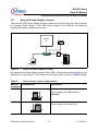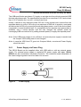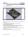
1
X E166 Ea sy K it Boa rd M anual, V.1.0, Nov. 2008
XE166 Family Easy Kit
Board REV. V3.1
M i c r o c o n t ro l le r s
N e v e r
s t o p
t h i n k i n g .
Edition 2008-11
Published by
Infineon Technologies AG
81726 München, Germany
© Infineon Technologies AG 2008.
All Rights Reserved.
Legal Disclaimer
The information given in this document shall in no event be regarded as a guarantee of conditions or
characteristics (“Beschaffenheitsgarantie”). With respect to any examples or hints given herein, any typical values
stated herein and/or any information regarding the application of the device, Infineon Technologies hereby
disclaims any and all warranties and liabilities of any kind, including without limitation warranties of noninfringement of intellectual property rights of any third party.
Information
For further information on technology, delivery terms and conditions and prices please contact your nearest
Infineon Technologies Office (www.Infineon.com).
Warnings
Due to technical requirements components may contain dangerous substances. For information on the types in
question please contact your nearest Infineon Technologies Office.
Infineon Technologies Components may only be used in life-support devices or systems with the express written
approval of Infineon Technologies, if a failure of such components can reasonably be expected to cause the failure
of that life-support device or system, or to affect the safety or effectiveness of that device or system. Life support
devices or systems are intended to be implanted in the human body, or to support and/or maintain and sustain
and/or protect human life. If they fail, it is reasonable to assume that the health of the user or other persons may
be endangered.
XE166 Family
Easy Kit Manual
XE166 Family Easy Kit
Revision History:
2008-11
V 1.0
Previous Version:
Page
Subjects (major changes since last revision)
We Listen to Your Comments
Any information within this document that you feel is wrong, unclear or missing at all?
Your feedback will help us to continuously improve the quality of this document.
Please send your proposal (including a reference to this document) to:
[email protected]
XE166 Easy Kit Board Manual
3
V 1.0, 2008-11
XE166 Family
Easy Kit Manual
Table of Contents
Page
1
Introduction - XE166 family . . . . . . . . . . . . . . . . . . . . . . . . . . . . . . . . . . . 5
2
2.1
2.2
2.3
2.4
2.4.1
2.4.2
2.5
2.6
2.6.1
General Information about XE166 Easy Kit Board . . . . . . . . . . . . . . . . . 6
Summary of Features . . . . . . . . . . . . . . . . . . . . . . . . . . . . . . . . . . . . . . . . . 6
Block Diagram . . . . . . . . . . . . . . . . . . . . . . . . . . . . . . . . . . . . . . . . . . . . . . . 7
Board Overview . . . . . . . . . . . . . . . . . . . . . . . . . . . . . . . . . . . . . . . . . . . . . . 8
DIP Switch S102 . . . . . . . . . . . . . . . . . . . . . . . . . . . . . . . . . . . . . . . . . . . . 10
Basic Startup Configuration for XE166F . . . . . . . . . . . . . . . . . . . . . . . . 10
Basic Startup Configuration for XE166FM . . . . . . . . . . . . . . . . . . . . . . . 11
USB Driver installation . . . . . . . . . . . . . . . . . . . . . . . . . . . . . . . . . . . . . . . . 12
Easy Kit Power Supply concept . . . . . . . . . . . . . . . . . . . . . . . . . . . . . . . . . 13
Power Supply via Power Plug . . . . . . . . . . . . . . . . . . . . . . . . . . . . . . . . 14
3
3.1
3.1.1
3.1.2
3.2
3.2.1
3.2.2
3.2.3
3.2.4
3.2.5
3.2.6
3.2.7
3.2.8
3.3
3.3.1
3.3.2
3.3.3
3.4
Information in Detail . . . . . . . . . . . . . . . . . . . . . . . . . . . . . . . . . . . . . . . .
Switch S102 . . . . . . . . . . . . . . . . . . . . . . . . . . . . . . . . . . . . . . . . . . . . . . . .
DIP Switch Setting XE166F . . . . . . . . . . . . . . . . . . . . . . . . . . . . . . . . . .
DIP Switch Setting XE166FM . . . . . . . . . . . . . . . . . . . . . . . . . . . . . . . .
Headers, Connectors and Components . . . . . . . . . . . . . . . . . . . . . . . . . .
USB Interface . . . . . . . . . . . . . . . . . . . . . . . . . . . . . . . . . . . . . . . . . . . .
CAN1/2 (X110, X111) . . . . . . . . . . . . . . . . . . . . . . . . . . . . . . . . . . . . . .
LIN Interface (X104) . . . . . . . . . . . . . . . . . . . . . . . . . . . . . . . . . . . . . . .
OCDS Interface . . . . . . . . . . . . . . . . . . . . . . . . . . . . . . . . . . . . . . . . . . .
DAP Interface . . . . . . . . . . . . . . . . . . . . . . . . . . . . . . . . . . . . . . . . . . . .
ADC . . . . . . . . . . . . . . . . . . . . . . . . . . . . . . . . . . . . . . . . . . . . . . . . . . . .
LEDs . . . . . . . . . . . . . . . . . . . . . . . . . . . . . . . . . . . . . . . . . . . . . . . . . . .
Serial Eeprom . . . . . . . . . . . . . . . . . . . . . . . . . . . . . . . . . . . . . . . . . . . .
Pin Definition and Location . . . . . . . . . . . . . . . . . . . . . . . . . . . . . . . . . . . .
XE167F/XE167FM - 144 - Pinout . . . . . . . . . . . . . . . . . . . . . . . . . . . . .
XE164F/XE164FM - 100 - Pinout . . . . . . . . . . . . . . . . . . . . . . . . . . . . .
XE162FM - 64 - Pinout . . . . . . . . . . . . . . . . . . . . . . . . . . . . . . . . . . . . .
Zero Ohm Resistors . . . . . . . . . . . . . . . . . . . . . . . . . . . . . . . . . . . . . . . . . .
15
16
16
17
18
18
18
19
19
20
21
21
21
22
22
24
26
27
4
4.1
4.2
4.3
Getting Started . . . . . . . . . . . . . . . . . . . . . . . . . . . . . . . . . . . . . . . . . . . . .
Power Supply . . . . . . . . . . . . . . . . . . . . . . . . . . . . . . . . . . . . . . . . . . . . . . .
OCDS Debugging Interface . . . . . . . . . . . . . . . . . . . . . . . . . . . . . . . . . . . .
USB Interface for UART support . . . . . . . . . . . . . . . . . . . . . . . . . . . . . . . .
29
30
31
31
5
Schematic . . . . . . . . . . . . . . . . . . . . . . . . . . . . . . . . . . . . . . . . . . . . . . . . . 32
XE166 Easy Kit Board Manual
4
V 1.0, 2008-11
XE166 Family
Easy Kit Manual
Introduction - XE166 family
1
Introduction - XE166 family
XE166 family - More performance, more Flash, better peripherals
With more than 15 successful years in the microcontroller market place, C166 has set
the standard for 16-bit architectures with the highest aggregate volume share of all
available 16-bit devices.
With its fast interrupt response and context switching, the C166 family is ideally suited
for automotive, industrial, mass storage and wired as well as wireless communications
applications.
Compared with the XC166, XE166 delivers more performance, more Flash memory,
more RAM, strongly enhanced peripherals and a complete DSP library.
MCU and DSP in a core
Infineon Technologies´ Real Time Signal Controller combines the traditional strengths of
a Microcontroller Unit (MCU) to control peripherals with the computing power of Digital
Signal Processors (DSP). All in one enhanced XE166 core. Together, the
Microcontroller's real-time capability and ease of use and the DSP's mathematical
performance and data throughput form a powerful singe-chip solution ideal for many
embedded applications.
For detailed technical information about the different derivatives please refer to the
XE166 family web pages on the Infineon Internet.
http://www.infineon.com/XE166
This document covers several product series.
–
–
–
–
–
XE167F Series
XE164F Series
XE167FM Series
XE164FM Series
XE162FM Series
XE166 Easy Kit Board Manual
5
V 1.0, 2008-11
XE166 Family
Easy Kit Manual
General Information about XE166 Easy Kit Board
2
General Information about XE166 Easy Kit Board
2.1
Summary of Features
–
–
–
–
–
–
–
Infineon’s XE166 Controller in TQFP144/100/64 Pin Package
High Speed CAN Transceivers, LIN Transceiver, USB to UART/JTAG bridge
8 Low Power Status LEDs
Easy access to all pins
5-DIP switches for configuration
On board USB to JTAG / UART interface
Powered via USB
Connectors
The XE166 Board offers a wide variety of connectors:
–
–
–
–
–
USB connector for ASC/JTAG Interface
4 pin header for LIN Transceiver
16-pin header for JTAG interface (OCDS)
10pin (2x5) header for CAN High Speed Transceiver (CAN1/CAN2)
10pin header for DAP interface
Components
–
–
–
–
–
–
–
–
–
–
Low-Drop Voltage Regulator TLE 4274
Step Down Voltage Regulator TLE 6365G (optional)
Four status LED´s for Power / RESET / JTAG
2 x CAN-Transceiver TLE 6251
LIN Transceiver TLE 7259
FT2232 Dual USB to UART/JTAG interface
SPI EEPROM 128 Kbit AT25128N
8 general purpose LEDs
Potentiometer for ADC
Reset switch
Zero Ohm Bridges
– Zero Ohm resistors give the flexibility to configure the systems functionality
XE166 Easy Kit Board Manual
6
V 1.0, 2008-11
XE166 Family
Easy Kit Manual
General Information about XE166 Easy Kit Board
2.2
Block Diagram
Voltage
Regulator
MultiCAN
CAN Transceiver
LIN Transceiver
TxD
LIN
EEPROM
XE166
CPU
RxD
USB
8 LEDs
OCDS1
USB To UART/
JTAG Bridge
XTAL
Figure 1
Block diagram of XE166 Easy Kit layout overview
XE166 Easy Kit Board Manual
7
V 1.0, 2008-11
XE166 Family
Easy Kit Manual
General Information about XE166 Easy Kit Board
2.3
Board Overview
1
P10.0
P10.7
1
1
DAP
OCDS1
5
Config
Infineon
XE166
Reset
1
Debug
Run
Debug
Active
Reset
1
CAN2
Power
supply
1
1
Power supply
Jumper
Figure 2
AN0(ADC1)
USB
CAN1
AN 0 ( ADC0)
1
LIN1
Power
Top View (basic components)
XE166 Easy Kit Board Manual
8
V 1.0, 2008-11
XE166 Family
Easy Kit Manual
X202
R151
R152
JP201
R113
C206
X106
CB214
R238
CB209
D209
R229
C203
R219
R124
R126
R125
R128
CB101
X104
X111
C202
R127
D205
U104
R134
R135
U206
CB226
C205
C106
R115
C105
R220
R114
C104
R221
CB103
R137
R156
R129
R130
R141
R132
R131
R212
R116
R133
R136
R155
R142
U105
D208
R222
C201
Q208
X110
X109
U106
R140
R138
R139
R237
R110
U205
D109
C107
R213
R239
X103
D207
L202
CB224
CB102
D202
R206
CB213
R154
Q205
R217
U202
CB229
X105
R236
Q201
D201
CB225
CB212
Q204
R232
CB211
CB223
R228
CB227
R216
CB210
S201
R225
CB220
X108
CB222
CB219
C207
R235
Q202
CB206
CB201
R207
L201
R210
R203
R202
CB204
Q203
R230
R205
P201
X112
R144
R146
R227
CB221
CB104
C204
R143
CB217
CB218
R226
R153
U107
R108
D108
R149
R107
D107
R147
R150
CB215
R218
R231
U201
R204
CB205
Y101
C103
R118
U203
R247
R233
R214
Y201
X204
CB216
U101
D204
R215
CB202
R117
R211
R209
R243
4 5
C102
Q206
CB228
R208
CB230
CB203
R201
R106
R104
D104
1 2 3
CB207
Q207
Figure 3
R145
X107
R148
R244
S102
R249 R241
R248
CB231
CB233
U207
R157
C101
R111
R234
CB232
D106
R103
D103
R119
R121
R242
R223
R240
U208
R123
R105
R102
D102
R245
R251
R246
X203
R224
R250
R252
R122
R112
R253
R109
R120
D105
R101
D101
General Information about XE166 Easy Kit Board
X201
Top view in detail
XE166 Easy Kit Board Manual
9
V 1.0, 2008-11
XE166 Family
Easy Kit Manual
General Information about XE166 Easy Kit Board
2.4
DIP Switch S102
Although most of the programmable features of the XE166 are selected by software
either during the initialization phase or repeatedly during program execution, some
features must be selected earlier because they are used for the first access of the
program execution.
These configurations are accomplished by latching the logic levels at a number of pins
at the end of the internal reset sequence.
DIP switch S102 allows to configure the startup setting of the XE166 during RESET. The
default System Startup Configuration is shown in Table 1. By default all DIP Switches
are OFF. The XE166 executes a standard start from internal Flash.
Table 1
Default configuration
Name in Default configuration
schematic
S102
Description
Startup configuration:
Standard start from internal Flash
(Default)
0
1
1
2
3
4
5
P10.0 P10.1 P10.2 P10.3 /TRST
2.4.1
Table 2
Basic Startup Configuration for XE166F
Basic Startup Configuration via External Circuitry
Startup Mode
CFG pins
P10 [3]
CFG pins
P10 [2]
CFG pins
P10 [1]
CFG pins
P10 [0]
P10 [3 : 0]1)
Internal Start from Flash
x
x
1
1
Standard UART Bootloader
x
1
1
0
Enhanced UART Bootloader
x
0
1
0
SSC Bootloader
1
0
0
1
CAN Bootloader
x
1
0
1
1)
x means that the level on the corresponding pin is irrelevant.
For more detailed information about the DIP switch setting please refer to Chapter 3.1.1,
Table 6.
XE166 Easy Kit Board Manual
10
V 1.0, 2008-11
XE166 Family
Easy Kit Manual
General Information about XE166 Easy Kit Board
2.4.2
Table 3
Basic Startup Configuration for XE166FM
Basic Startup Configuration with debug support
Startup Mode
Internal Start from Flash
Debug
Interface
CFG pins P10 [3:0]
1)
TRST=1
JTAG pos.B
x
0
1
1
DAP pos.1
x
1
0
0
from Flash 2)
x
1
1
1
DAP pos.0
0
0
0
1
DAP pos.2
0
1
0
1
1)
x means that the level on the corresponding pin is irrelevant.
2)
A defined location in Flash (C0’01F0H) must contain a value (2 Bytes) for DBGPRR register and the next wordlocation (C0’01F2H) must contain the inverse value.
If the inverse-condition does not match - the value is considered as invalid and JTAG pins at position A are
configured by default.
Table 4
Basic Startup Configuration via External Circuitry
Configuration pins 1)
Startup Mode
TRST
P10 [3 : 0]
Internal Start from Flash
0
x
x
x
x
UART Bootloader 2.x 2)
1
x
0
1
0
UART Bootloader 7.x 3)
1
x
1
1
0
SSC Bootloader
1
1
0
0
1
CAN Bootloader
1
1
1
0
1
1)
x means that the level on the corresponding pin is irrelevant.
2)
2.x means: TxD (transmit data) at P2.3 pin, RxD (receive data) at P2.4 pin.
3)
7.x means: TxD (transmit data) at P7.3 pin, RxD (receive data) at P7.4 pin.
For more detailed information about the DIP switch setting please refer to Chapter 3.1.2,
Table 7.
XE166 Easy Kit Board Manual
11
V 1.0, 2008-11
XE166 Family
Easy Kit Manual
General Information about XE166 Easy Kit Board
2.5
USB Driver installation
All USB-Transaction are realized by the USB-Software running on a Host-Computer.
The USB-Device driver is communicating with the Equipment connected to the
Computer.
The driver for Easy Kit USB interface will be delivered with a Software called DAS
(Device Access Server). The goal of the DAS architecture is to provide one single
interface for all types of tools, which fulfills all performance and reliability needs.
Additionally a driver for a virtual COM port will be installed.
Find out more about DAS on the Infineon Web page:
http://www.infineon.com/DAS
This DAS Software can be found on the Easy Kit CD under Tools. A DAS Software
Version 2.6.1 or higher need to be used for the Easy Kit.
XE166 Easy Kit Board Manual
12
V 1.0, 2008-11
XE166 Family
Easy Kit Manual
General Information about XE166 Easy Kit Board
2.6
Easy Kit Power Supply concept
The Easy Kit USB Power Supply concept enables the user to work with the Kit without
an external Power Supply. If the USB power supply is not sufficient an additional
regulated DC power supply can be used.
XE166
CPU
Power
LED
1
5V
DC
X502
Power Supply
USB Supply
6 … 12V
5V
Figure 4
Easy Kit Power Supply concept
By means of the Power Supply Jumper X502, USB, or the external power Supply can be
selected to run the Easy Kit. The Setup for the Jumper X502 is shown in Table 5 below.
Table 5
Power Supply Jumper configuration
Name in
Configuration
schematic
Description
X502
Power Supply via USB Interface
(Default)
1
2
3
X502
Power Supply via Power Plug
1
XE166 Easy Kit Board Manual
2
3
13
V 1.0, 2008-11
XE166 Family
Easy Kit Manual
General Information about XE166 Easy Kit Board
The USB specification provides a 5 V supply on a single wire from which connected USB
devices may draw power. The specification provides for no more than 5.25 V and no less
than 4.35 V between the +ve and -ve bus power lines.
Initially, a device is only allowed to draw 100 mA. It may request more current from the
upstream device in units of 100 mA up to a maximum of 500 mA. In practice, most ports
will deliver the full 500 mA or more before shutting down power, even if the device hasn't
requested it or even identified itself. If a (compliant) device requires more power than is
available, then it cannot operate until the user changes the network (either by
rearranging USB connections or by adding external power) to supply the required power.
Note: If the USB power supply is not sufficient, an external power supply is needed and
the Jumper X502 setting need to be changed.
Note: In case the USB Host PC goes into Suspend Mode, an external Power Supply
should be used.
2.6.1
Power Supply via Power Plug
The XE166 Board can be supplied either with USB cable or with an external power
supply. For external power supply a regulated DC power supply with max. 12Volt/
400mA can be connected to the power connector. The maximum power dissipation of
the used voltage regulator has to be taken into account.
Figure 5
Power Supply
XE166 Easy Kit Board Manual
14
V 1.0, 2008-11
XE166 Family
Easy Kit Manual
Information in Detail
3
Information in Detail
The XE166 family supports variety of start-up modes, allowing the user to make
selections in three aspects:
• Main functionality - where from the user code will be started (on-chip Flash, PSRAM,
external memory);
• Optionally - a way for initial code-downloading into PSRAM before to start it:
– From an external host via a communication interface - UART, CAN, SSC;
– From Stand-by RAM (SBRAM) - after exiting a power-saving mode;
• Debug-related - either debugging will be possible, and if Yes - which debug-interface
to use (JTAG, DAP, selectable pin-assignments).
The Easy Kit Board Manual covers only a limit numbers of start-up modes. For all
possible start-up modes please refer to the corresponding user manual.
XE166 Easy Kit Board Manual
15
V 1.0, 2008-11
XE166 Family
Easy Kit Manual
Information in Detail
3.1
Switch S102
3.1.1
DIP Switch Setting XE166F
Table 6
DIP Switch Settings for S102
Name in Default configuration
schematic
S102
Description
Startup configuration:
Standard start from internal Flash
OFF-OFF-xx-xx-xx
On
Off
1
2
3
4
5
S102
Startup configuration:
Bootstrap loader ASC
ON-OFF-OFF-xx-xx
On
Off
1
2
3
4
5
S102
Startup configuration:
Enhanced bootstrap loader ASC
ON-OFF-ON-xx-xx
On
Off
1
2
3
4
5
S102
Startup configuration
Bootstrap loader CAN
OFF-ON-OFF-xx-xx
On
Off
1
2
3
4
5
S102
Startup configuration
Bootstrap loader SSC
OFF-ON-ON-OFF-xx
On
Off
1
2
3
4
5
S102
XE166 Easy Kit Board Manual
Startup configuration
All other positions are reserved
16
V 1.0, 2008-11
XE166 Family
Easy Kit Manual
Information in Detail
3.1.2
DIP Switch Setting XE166FM
Table 7
DIP Switch Settings for S102
Name in Default configuration
Description
schematic
S102
Startup configuration:
On
Standard start from internal Flash
xx-xx-xx-xx-OFF
Off
1
2
3
5
4
S102
Startup configuration:
Bootstrap loader ASC For XE167FM and
XE164FM
ON-OFF-OFF-xx-ON
On
Off
1
2
3
5
4
S102
Startup configuration:
Bootstrap loader ASC for XE162FM
ON-OFF-ON-xx-ON
On
Off
1
2
3
4
5
S102
Startup configuration:
DAP Debug Mode (Pos.1)
ON-ON-OFF-xx-ON
On
Off
1
2
3
4
5
S102
Startup configuration:
JTAG Debug Mode (Default)
OFF-OFF-OFF-xx-ON
On
Off
1
2
3
4
5
S102
Startup configuration:
Bootstrap loader CAN
OFF-ON-OFF-OFF-ON
On
Off
1
2
3
4
5
S102
Startup configuration:
Bootstrap loader SSC
OFF-ON-ON-OFF-ON
On
Off
1
2
3
4
5
S102
XE166 Easy Kit Board Manual
Startup configuration
All other positions are reserved
17
V 1.0, 2008-11
XE166 Family
Easy Kit Manual
Information in Detail
3.2
Headers, Connectors and Components
3.2.1
USB Interface
The USB connector is used for connection to a PC. Via the USB it is possible to power
the board, using the USIC0 Channel 0 as serial connection via USB and Debugging via
DAS. For the pinout of USB socket see Figure 6.
Figure 6
3.2.2
2 (D-)
1 (Vbus)
3 (D+)
4 (GND)
On-board header (P201)
CAN1/2 (X110, X111)
On the board are two CAN transceiver connected to the MultiCAN on XE166 node 0 and
1. The transceivers are connected to two IDC10 plug. For the pinout of IDC10 plug see
Figure 7. You can use a IDC female connector with crimpconnector, flat cable and SUBD 9 plug with crimpconnector to have a 1:1 adapter to SUB-D 9.
CAN2L
GND
Figure 7
1
2
3
4
5
6
7
8
9
10
GND
CAN2H
VDDP
On-board header (X110,X111)
Note: If the Board is equipped with a XE162FM in a 64 Pin package the CAN2 interface
is disabled. To enable remove R238 and solder R136. In this case Usic 0 channel
0 is not avalible on Pin 2.4 .
XE166 Easy Kit Board Manual
18
V 1.0, 2008-11
XE166 Family
Easy Kit Manual
Information in Detail
3.2.3
LIN Interface (X104)
Figure 8
3.2.4
4
VBat
Vs
3
2
Bus
GND
1
The board has a connector with 4 pins for LIN. For the pinout of the connector see Figure
8. The LIN transceiver is connected to USIC1 Channel 0 module of the CPU.
On-board header (X104)
OCDS Interface
The OCDS1 signals are connected to the IDC16 plug (X202). For pinout of the
connector see Figure 9. You can connect any debugger to this connector.
The signals /BRKIN and /BRKOUT are not connected per default. If you need this signals
in the connector then assemble R225 and R226 with a 0R resistor.
If you connect a debug hardware make sure that the MiniWiggler circuit is not activ
(ACTIV LED is off) and on the DAP connector (X204) is no hardware connected or the
hardware is tristated.
If the ACTIV LED is on, then stop the active DAS Server JTAG over USB Chip and/or
remove the USB connection to the PC.
XE166 Easy Kit Board Manual
19
V 1.0, 2008-11
XE166 Family
Easy Kit Manual
Information in Detail
Vcc
TMS
1
2
3
4
5
6
7
8
9
10
GND
TDO
CPUCLK
GND
TDI
/MR
/BRK_OUT
/TRST
GND
TCLK
11 12
/OCDS_E
/BRK_IN
13 14
15 16
Figure 9
3.2.5
On-board header X202
DAP Interface
The board comes with a DAP connector (X204). For pinout of this connector see Figure
10. You can connect a DAP hardware here. If you use this connector make sure that the
MiniWiggler is not activ (ACTIV LED is off) and a connected OCDS1 hardware is
disconnected or tristated.
VREF
DAP1
1
2
3
4
5
6
7
8
9
10
GND
DAP0
USER0_IO
GND
USER1_IN
GND
Figure 10
/RESET
On-board header X204
XE166 Easy Kit Board Manual
20
V 1.0, 2008-11
XE166 Family
Easy Kit Manual
Information in Detail
3.2.6
ADC
On AN0 (ADC0) is a 10K potentiometer (R113) connected. You can apply a voltage
between VAGND0 and VAREF0 to the AN0 channel via this potentiometer.
R116 is connected to AN0 (ADC1). The potentiometer is not assembled by default. You
can assembled a potentiometer to use this connection. The footprint is prepared for a
Burns potentiometer typ 3006.
3.2.7
LEDs
Port 10 pin 0 up to pin 7 are connected to single LED’s (D101... D108) and can be
controlled by Software. This status LED’s are low active.
Table 8
LEDs description
LED number
Description
D201 (red)
Debug Run Mode (switched by
DAS Server)
D202 (green)
Debug Active (Mini Wiggler circuit
active)
D207 (red)
Power On Reset Active
D208 (green)
Board Voltage 5 Volt
D101 - D108 (yellow)
Status of P10L
3.2.8
Serial Eeprom
By default the USIC0 Channel1 of the XE166 is connected to a serial EEPROM with a
size of 128K (16.384 x 8). If the SSC bootstrap loader is needed the four resistors have
been reconfigured as described in table 8.
Table 9
Serial Eeprom interface
Default Setting:
SSC (USIC0 Channel 1)
SSC bootstrap loader (USIC0
Channel 0)
P10.5 (SCK) with R143
P2.5 (SCK) replace R143 with
R144
P10.0 (SI) with R145
P2.4 (SI) replace R145 with R146
P10.7 (SO) with R147
P2.3 (SO) replace R147 with R148
P2.7 (CS) with R149
P2.6 (CS) replace R149 with R150
XE166 Easy Kit Board Manual
21
V 1.0, 2008-11
XE166 Family
Easy Kit Manual
Information in Detail
XE167F/XE167FM - 144 - Pinout
TESTM
P7.2
P8.4
TRST
P8.3
P7.0
P7.3
P8.2
P7.1
P7.4
P8.1
P8.0
VDDIM
P6.0
P6.1
P6.2
P6.3
VDDPA
P15.0
P15.1
P15.2
P15.3
P15.4
P15.5
P15.6
P15.7
V AREF1
V AREF0
V AGND
P5.0
P5.1
P5.2
P5.3
VDDPB
VSS
VDDI1
1
2
3
4
5
6
7
8
9
10
11
12
13
14
15
16
17
18
19
20
21
22
23
24
25
26
27
28
29
30
31
32
33
34
35
36
108
107
106
105
104
103
102
101
100
99
98
97
96
95
94
93
92
91
90
89
88
87
86
85
84
83
82
81
80
79
78
77
76
75
74
73
XE167
VDDPB
P3.7
P0.7
P10.7
P3.6
P10.6
P0.6
P3.5
P10.5
P3.4
P10.4
P3.3
P0.5
P10.3
P2.10
P3.2
Tref (1)
VDDI1
P0.4
P10.2
P3.1
P0.3
P10.1
P3.0
P10.0
P0.2
P2.9
P4.7
P2.8
P0.1
P2.7
P4.6
P4.5
P0.0
VDDPB
VSS
Figure 11
VDDPB
P2.0
P2.1
P11.4
P2.2
P11.3
P4.0
P2.3
P11.2
P4.1
P2.4
P11.1
P11.0
P2.5
P4.2
P2.6
P4.4
P4.3
VDDI1
P5.4
P5.5
P5.6
P5.7
P5.8
P5.9
P5.10
P5.11
P5.12
P5.13
P5.14
P5.15
P2.12
P2.11
P11.5
VSS
VDDPB
37
38
39
40
41
42
43
44
45
46
47
48
49
50
51
52
53
54
55
56
57
58
59
60
61
62
63
64
65
66
67
68
69
70
71
72
VDDPB
144
143
142
141
140
139
138
137
136
135
134
133
132
131
130
129
128
127
126
125
124
123
122
121
120
119
118
117
116
115
114
113
112
111
110
109
VSS
VDDPB
P9.5
P9.4
P1.3
P10.13
P9.3
P10.12
P1.2
P9.2
P10.11
P10.10
P1.1
P10.9
P9.1
P10.8
P9.0
P1.0
3.3.1
P8.5
P8.6
ESR0
ESR2
ESR1
PORST
XTAL1
XTAL2
P1.7
P9.7
P1.6
P9.6
P1.5
P10.15
P1.4
P10.14
Pin Definition and Location
VDDPB
3.3
Pinout of the144 Pin device
Note: (1) For the XE166FM Series the Tref pin has been replaced by P2.13.
XE166 Easy Kit Board Manual
22
V 1.0, 2008-11
XE166 Family
Easy Kit Manual
Information in Detail
12
11
10
9
8
7
6
5
4
3
2
1
P0.7
P10.6
P10.5
P3.3
P2.10
VDDI1
P3.1
P3.0
P2.9
P0.1
P4.5
Vss
A
P3.7
P3.6
P3.5
P10.4
P10.3
TREF
P10.2
P10.1
P0.2
P2.8
P4.6
VDDPB
B
VDDPB
P10.7
P0.6
P3.4
P0.5
P3.2
P0.4
P0.3
P10.0
P4.7
P2.7
P0.0
C
B
C
1
Vss
VDDPB
P1.0
VDDPB
P4.3
P4.4
12
2
P9.0
P10.8
P9.1
P2.6
P4.2
P2.5
11
3
P10.9
P1.1
P10.10
P11.0
P11.1
P2.4
10
4
P10.11
P9.2
P1.2
P4.1
P11.2
P2.3
9
5
P10.12
P9.3
P10.13
P4.0
P11.3
P2.2
8
6
P1.3
P9.4
P9.5
P11.4
P2.1
P2.0
7
7
VDDI1
P10.14
P1.4
VDDI1
P11.5
P2.11
6
8
P10.15
P1.5
P9.6
P2.12
P5.15
P5.14
5
9
P1.6
P9.7
P1.7
P5.13
P5.12
P5.11
4
10
XTAL2
XTAL1 /PORST
P5.10
P5.9
P5.8
3
11
ESR1
ESR2
ESR0
P5.7
P5.6
P5.5
2
12
P8.6
P8.5
VDDPB
P5.4
VDDPB
Vss
1
C
B
A
X108
A
X106
X107
X105
Figure 12
XE167
/TESTM
/TRST
P7.3
P7.4
VDDIM
P6.2
P15.0
P15.3
P15.6
VAREF1
P5.1
VDDPB
VDDPB
P8.4
P7.0
P7.1
P8.0
P6.1
VDDPA
P15.2
P15.5
VAREF2
P5.0
P5.3
Vss
P7.2
P8.3
P8.2
P8.1
P6.0
P6.3
P15.1
P15.4
P15.7
VAGND
P5.2
1
2
3
4
5
6
7
8
9
10
11
12
Pin connector of the144 pin device
XE166 Easy Kit Board Manual
23
V 1.0, 2008-11
XE166 Family
Easy Kit Manual
Information in Detail
VDDP
VSS
P1.3
P10.13
P10.12
P1.2
P10.11
P10.10
P1.1
P10.9
P10.8
P1.0
100
99
98
97
96
95
94
93
92
91
90
89
88
87
86
85
84
83
82
81
80
79
78
77
76
VDDI
ESR0
ESR1
PORST
XTAL1
XTAL2
P1.7
P1.6
P1.5
P10.15
P1.4
P10.14
XE164F/XE164FM - 100 - Pinout
VDDP
3.3.2
VSS
VDDP
TESTM
P7.2
TRST
P7.0
P7.3
P7.1
P7.4
VDDI
P6.0
P6.1
P6.2
VDDP
P15.0
P15.2
P15.4
P15.5
P15.6
VAREF
VAGND
P5.0
P5.2
P5.3
75
74
73
72
71
70
69
68
67
66
65
64
63
62
61
60
59
58
57
56
55
54
53
52
51
XE164
VDDP
P0.7
P10.7
P10.6
P0.6
P10.5
P10.4
P0.5
P10.3
P2.10
Tref (1)
VDDI
P0.4
P10.2
P0.3
P10.1
P10.0
P0.2
P2.9
P2.8
P0.1
P2.7
P0.0
VDDP
VSS
Figure 13
VDDP
P2.0
P2.1
P2.2
P4.0
P2.3
P4.1
P2.4
P2.5
P4.2
P2.6
P4.3
VDDI
P5.4
P5.5
P5.8
P5.9
P5.10
P5.11
P5.13
P5.15
P2.12
P2.11
VSS
VDDP
26
27
28
29
30
31
32
33
34
35
36
37
38
39
40
41
42
43
44
45
46
47
48
49
50
VDDP
1
2
3
4
5
6
7
8
9
10
11
12
13
14
15
16
17
18
19
20
21
22
23
24
25
Pinout of the 100 pin device
Note: (1) For the XE166FM Series the Tref pin has been replaced by P2.13.
XE166 Easy Kit Board Manual
24
V 1.0, 2008-11
XE166 Family
Easy Kit Manual
Information in Detail
12
11
10
9
8
7
6
5
4
3
2
1
P0.7
P10.6
P10.5
nc
P2.10
VDDI1
nc
nc
P2.9
P0.1
nc
Vss
A
nc
nc
nc
P10.4
P10.3
TREF
P10.2
P10.1
P0.2
P2.8
nc
VDDPB
B
VDDPB
P10.7
P0.6
nc
P0.5
nc
P0.4
P0.3
P10.0
nc
P2.7
P0.0
C
A
B
C
1
Vss
VDDPB
P1.0
VDDPB
P4.3
nc
12
2
nc
P10.8
nc
P2.6
P4.2
P2.5
11
3
P10.9
P1.1
P10.10
nc
nc
P2.4
10
4
P10.11
nc
P1.2
P4.1
nc
P2.3
9
5
P10.12
nc
P10.13
P4.0
nc
P2.2
8
6
P1.3
nc
nc
nc
P2.1
P2.0
7
7
VDDI1
P10.14
P1.4
VDDI1
nc
P2.11
6
8
P10.15
P1.5
nc
P2.12
P5.15
nc
5
9
P1.6
nc
P1.7
P5.13
nc
P5.11
4
10
XTAL2
P5.10
P5.9
P5.8
3
11
ESR1
nc
ESR0
nc
nc
P5.5
2
12
nc
nc
VDDPB
P5.4
VDDPB
Vss
1
C
B
A
X106
X107
XE164
X108
XTAL1 /PORST
X105
Figure 14
/TESTM
/TRST
P7.3
P7.4
VDDIM
P6.2
P15.0
nc
P15.6
VAREF1
P5.1
VDDPB
VDDPB
nc
P7.0
P7.1
nc
P6.1
VDDPA
P15.2
P15.5
nc
P5.0
P5.3
Vss
P7.2
nc
nc
nc
P6.0
nc
nc
P15.4
nc
VAGND
P5.2
1
2
3
4
5
6
7
8
9
10
11
12
Pin connector of the 100 pin device
XE166 Easy Kit Board Manual
25
V 1.0, 2008-11
XE166 Family
Easy Kit Manual
Information in Detail
3.3.3
Figure 15
XE162FM - 64 - Pinout
Pinout of the 64 pin device
XE166 Easy Kit Board Manual
26
V 1.0, 2008-11
XE166 Family
Easy Kit Manual
Information in Detail
3.4
Zero Ohm Resistors
For configuration purposes several zero ohm resistors have been implemented. The
functionality of these resistors are shown in the table below.
Table 10
Zero Ohm Resistors
Component
Name in
schematic
TLE 7259G
(LIN Transceiver Board) R124
R125 / R126
TLE 6251DS
(CAN Transceiver)
R129 / R130
R136 / R137
R155 / R156
R131
R138
R135
R142
R133 / 134
R140 / 141
Microcontroller XE166
Analog reference
R220 / R221
R219
Voltage supply
R212 / R229
JTAG X202
R225
R226
AT25128N
(Serial EEPROM)
R143 / R145
R147 / R149
R144 / R146
R148 / R150
XE166 Easy Kit Board Manual
Description
enable / disable
connect / disconnect
connect / disconnect (CAN1)
connect / disconnect (CAN2) or
connect / disconnect (CAN2)
enable / disable (CAN1)
enable / disable (CAN2)
supply Bus voltage internal / external (CAN1)
supply Bus voltage internal / external (CAN2)
connect Bus / disconnect Bus (CAN1)
connect Bus / disconnect Bus (CAN2)
change of analog reference source
change of voltage supply
/BRKIN (optional)
/BRKOUT (optional)
connect to USIC1 Channel1
connect to USIC1 Channel1
connect to SSC bootstrap loader (U0C0)
connect to SSC bootstrap loader (U0C0)
27
V 1.0, 2008-11
XE166 Family
Easy Kit Manual
Information in Detail
Table 10
Zero Ohm Resistors
Component
Name in
schematic
Status LED´s
R109
Oscillator circuit
R117/R118
FT2232D
(USB to UART / JTAG
Bridge):
R224
R223
JTAG-Option:
R242-R246
R247-R253
DAP-Option:
R242-R246
R247-R252
R253
ASC Bootloader:
144Pin / 100 Pin
R236-R237
R238-R239
Other
R236-R237
R238-R239
Description
connect / disconnect LED´s to 5 V
oscillator gain
/BRKOUT (optional)
/BRKIN (optional)
assembled with 0R
open
open
assembled with 0R
assembled with 47K
assembled with 0R
open
open
assembled with 0R
U203:
R210
For internal use only
EEPROM 93LC46B:
R207
If ORG functionality is needed
XE166 Easy Kit Board Manual
28
V 1.0, 2008-11
XE166 Family
Easy Kit Manual
Getting Started
4
Getting Started
For the successful start up of the XE166 Easy Kit, the following items should be done:
Figure 16
XE166 Easy Kit (144-Pin)
By default a HELLO WORLD program can be executed. The following steps are needed
to be successful.
1. Verify that the Jumper JP201 is in position 1-2 (powered via USB).
2. Connect USB cable with starterkit and PC.
3. Install DAS driver from starterkit CD.
4. Verify if the standard start mode is selected as described in chapter 3.1.
5. LED D105 connected with P10.0 should flash, otherwise press the Reset button.
6. Verify which COM port is activated for the FTDI - chip.
7. Execute the monitor program MTTTY from the starterkit CD.
8. Select the corresponding COM port, 19200 Baud, none parity, 8 data Bit, one stop bit,
parser off.
9. Start connection (File/connect).
10.Press Reset button on the starterkit, Hello World program is running .
XE166 Easy Kit Board Manual
29
V 1.0, 2008-11
XE166 Family
Easy Kit Manual
Getting Started
Figure 17
4.1
Monitor Program MTTTY with Hello World program
Power Supply
If more current is needed, a regulated DC power supply with max. 12 Volts should be
connected to the power connector. The maximum power dissipation of the used voltage
regulator has to be taken into account. By default one green LED should be active. It
indicates that the embedded voltage regulator supply the microcontroller.
Please Note, the power supply is not part of the delivery !
Figure 18
Power Supply Connector
XE166 Easy Kit Board Manual
30
V 1.0, 2008-11
XE166 Family
Easy Kit Manual
Getting Started
4.2
OCDS Debugging Interface
The XE166 Easy Kit offers two types of JTAG interfaces. With the FTDI chip an on board
USB JTAG wiggler has been implemented. Further the USB interface allows to emulate
a USB to UART bridge. Both can be done at the same time.
A simple 16 pin JTAG header can be used to connect a debugger from one of Infineon’s
tool suppliers. Both systems include an On-Chip Debug Support (OCDS) system, which
provides convenient debugging, controlled directly by an external device via debug
interface pins.
4.3
USB Interface for UART support
The USB connector is used for connection to a PC. Via the USB it is possible to power
the board, using the ASC0 as serial connection via USB and Debugging via DAS. For
the pinout of USB socket see Figure 6.
NOTE: Before connecting the board to the PC, make sure that the actual DAS software
is installed on the PC. For actual DAS software please contact your local FAE.
The latest version of the software can also be found on the
www.infineon.com/DAS
XE166 Easy Kit Board Manual
31
V 1.0, 2008-11
A
B
C
D
10K
10K_opt
1K5
R108
1K5
R107
1K5
R106
1K5
R105
1K5
R104
1K5
R103
1K5
R102
R101
P10.15
P1.6
XTAL2
ESR1
P8.6
P10.8
P1.1
P9.2
P9.3
P9.4
P10.14
P1.5
P9.7
XTAL1
ESR2
P8.5
1
D108
D107
D106
D105
D104
D103
D102
D101
LY T67K
LY T67K
LY T67K
LY T67K
LY T67K
LY T67K
LY T67K
LY T67K
VDDP0
VDDP0
VDDI1
GND
P10.7
P10.6
P10.5
P10.4
P10.3
P10.2
P10.1
P10.0
P1.0
P9.1
P10.10
P1.2
P10.13
P9.5
P1.4
P9.6
P1.7
/PORST
ESR0
CPUCON4_opt
3
6
9
12
15
18
21
24
27
30
33
36
X108C
CPUCON4_opt
2
5
8
11
14
17
20
23
26
29
32
35
X108B
C105
100n
P15.0
VAGND
CPUCON4_opt
1
4
7
10
13
16
19
22
25
28
31
34
C104
100n
P5.0
VAGND
P9.0
P10.9
P10.11
P10.12
P1.3
100R
X108A
VAGND
1K5
100R
R116 2 R115
VAREF2
VAGND
1
3
R109
0R
+5V
1
3
R113 2 R114
R154
10K
10K
R111
75
79
83
87
90
96
102
106
111
116
120
124
129
131
133
135
55
56
58
61
64
67
69
78
80
82
94
52
51
P0.0
P0.1
P0.2
P0.3
P0.4
P0.5
P0.6
P0.7
P1.0
P1.1
P1.2
P1.3
P1.4
P1.5
P1.6
P1.7
P2.0
P2.1
P2.2
P2.3
P2.4
P2.5
P2.6
P2.7
P2.8
P2.9
P2.10
P2.11
P2.12
/TESTM 3
TREF_P2.13 92
/PORST 138
/TRST
6
R110
0R
+5V
ESR2
ESR1
ESR0
/TRST
GND
2
P2.0
P2.1
P2.2
P2.3
P2.4
P2.5
P2.6
P2.7
P2.8
P2.9
P2.10
P2.11
P2.12
P1.0
P1.1
P1.2
P1.3
P1.4
P1.5
P1.6
P1.7
P0.0
P0.1
P0.2
P0.3
P0.4
P0.5
P0.6
P0.7
2
Y101
opt
R118
C102 8MHz
18pF
R117
0R
GND
TESTM
TREF / P2.13
PORST
TRST
GND
C101
10n_opt
R112
TREF_P2.13 10K
+5V
XTAL2
C103
18pF
XTAL1
GND
XTAL2
1
3
3
85
88
93
97
99
101
104
107
P3.0
P3.1
P3.2
P3.3
P3.4
P3.5
P3.6
P3.7
VAREF1
XTAL1
2
ESR0
ESR1
ESR2
141
139
140
ESR0
ESR1
ESR2
136
XTAL2
137
XTAL1
60
63
68
71
70
76
77
81
P3.0
P3.1
P3.2
P3.3
P3.4
P3.5
P3.6
P3.7
P15.7
P15.6
P15.5
P15.4
P15.3
P15.2
P15.1
P15.0
28
27
26
25
24
23
22
21
P15.7
P15.6
P15.5
P15.4
P15.3
P15.2
P15.1
P15.0
P4.0
P4.1
P4.2
P4.3
P4.4
P4.5
P4.6
P4.7
P11.5
P11.4
P11.3
P11.2
P11.1
P11.0
53
57
59
62
65
66
P11.5
P11.4
P11.3
P11.2
P11.1
P11.0
4
P10.15
P10.14
P10.13
P10.12
P10.11
P10.10
P10.9
P10.8
130
128
123
121
118
117
115
113
4
P6.3
P6.2
P6.1
P6.0
P7.4
P7.3
P7.2
P7.1
P7.0
P8.6
P8.5
P8.4
P8.3
P8.2
P8.1
P8.0
P9.7
P9.6
P9.5
P9.4
P9.3
P9.2
P9.1
P9.0
P10.7
P10.6
P10.5
P10.4
P10.3
P10.2
P10.1
P10.0
P10.15
P10.14
P10.13
P10.12
P10.11
P10.10
P10.9
P10.8
P5.0
P5.1
P5.2
P5.3
P5.4
P5.5
P5.6
P5.7
P5.8
P5.9
P5.10
P5.11
P5.12
P5.13
P5.14
P5.15
P4.0
P4.1
P4.2
P4.3
P4.4
P4.5
P4.6
P4.7
32
32
33
34
35
39
40
41
42
43
44
45
46
47
48
49
50
XE166 Easy Kit Board Manual
P5.0
P5.1
P5.2
P5.3
P5.4
P5.5
P5.6
P5.7
P5.8
P5.9
P5.10
P5.11
P5.12
P5.13
P5.14
P5.15
P10.7
P10.6
P10.5
P10.4
P10.3
P10.2
P10.1
P10.0
P9.7
P9.6
P9.5
P9.4
P9.3
P9.2
P9.1
P9.0
P8.6
P8.5
P8.4
P8.3
P8.2
P8.1
P8.0
P7.4
P7.3
P7.2
P7.1
P7.0
P6.3
P6.2
P6.1
P6.0
134
132
126
125
122
119
114
112
142
143
5
7
10
13
14
12
9
4
11
8
19
18
17
16
XC2XXX
R157
R122
GND
105
103
100
98
95
89
86
84
U101A
+5V
R121
R120
R119
VDDI1
GND
VDDP0
VAREF1
VDDIM
VAREF2
VDDP1
VDDP0
VAGND
GND
1K
220R
220R
220R
220R
S102
1
4
7
10
13
16
19
22
25
28
31
34
1
4
7
10
13
16
19
22
25
28
31
34
2
5
8
11
14
17
20
23
26
29
32
35
2
5
8
11
14
17
20
23
26
29
32
35
P5.6
P5.9
P5.12
P5.15
P11.5
P2.1
P11.3
P11.2
P11.1
P4.2
P4.3
3
6
9
12
15
18
21
24
27
30
33
36
3
6
9
12
15
18
21
24
27
30
33
36
X105C X106C
P11.4
P4.0
P4.1
P11.0
P2.6
P5.4
P5.7
P5.10
P5.13
P2.12
1
4
7
10
13
16
19
22
25
28
31
34
2
5
8
11
14
17
20
23
26
29
32
35
X107A X107B
5
VDDP0
VDDI1
VDDP0
VDDP0
P4.6
P2.8
P0.2
P10.1
P10.2
TREF_P2.13
P10.3
P10.4
P3.5
P3.6
P3.7
CPUCON3_opt CPUCON3_opt
P2.10
P3.3
P10.5
P10.6
P0.7
P4.5
P0.1
P2.9
P3.0
P3.1
CPUCON1_opt CPUCON2_opt
P5.1
P6.2
P15.0
P15.3
P15.6
/TESTM
/TRST
P7.3
P7.4
CPUCON1_opt CPUCON2_opt
P5.0
P5.3
P15.2
P15.5
P8.4
P7.0
P7.1
P8.0
P6.1
X105B X106B
GND
GND
P2.10
P2.8
P10.4
P10.0
P10.1
P10.2
P10.3
/TRST
P5.5
P5.8
P5.11
P5.14
P2.11
P2.0
P2.2
P2.3
P2.4
P2.5
P4.4
I2C_opt
1
2
3
X112
X105A X106A
PORT[0..15]
opt
R123
CONFIG
1
2
3
4
5
CPUCON1_opt CPUCON2_opt
P5.2
P7.2
P8.3
P8.2
P8.1
P6.0
P6.3
P15.1
P15.4
P15.7
10
9
8
7
6
5
1
6
VDDP0
+5V
0R
5
3
4
1
2
GND
R124
3
6
9
12
15
18
21
24
27
30
33
36
X107C
0R
R149
0R
R138
TLE6251DS
1
6
5
2
TXD CANL
GND STB
VCC SPLIT
RXD CANH
U106
0R
R131
TLE6251DS
TXD CANL
GND STB
7
HOLD
WP
VCC
GND
AT25128N-10SI2.7
CS
SCK
SI
SO
R139
120R
7
3
8
4
0R
0R
R141
R140
X110
SPLIT_CAN2_opt
0R
0R
R134
R133
X109
SPLIT_CAN1_opt
R132
120R
3
R128
1K
D109
CAN2
1
3
5
7
9
X103
CAN1
1
3
5
7
9
X111
GND
CB104
100n
+5V
1
of
3
Infineon Technologies AG
7
AIM MC ACE 1
Number:
Am Campeon 1-12
D-85579 Neubiberg
Revision: 3.0
Date:
20-Mar-2008
Tel.: +49-89-234-0
File: G:\Technical_Support\P11\XC2XXX\EDA\Easy Kit\Easy Kit XC2XXX.Ddb - Mixed V3.0\Main.Sch
Sheet:
2
R151
10K
2
4
6
8
10
2
4
6
8
10
GND
1
C106
22µF/50V BAT54-04
GND
C107
1n
GND
CB101
100n
GND
U107
6
8
5
7
6
8
5
7
7
8
6
Easy Kit XC2XXX CPU and On Board IO's
0R_opt
R150
0R_opt
R148
0R_opt
R147
0R_opt
R144
R146
0R
1
2
3
4
GND
0R
R145
0R
100n
1
2
GND
CB103 +5V
R143
0R_opt
0R
R156
0R_opt
R137
0R
R155
GND
R136
0R
0R
R130
VS
INH
BUS
VCC SPLIT
RXD CANH
U105
TLE7259G
GND
WK
TXD
RXD
EN
U104
CB102 +5V
GND
3
R129 100n
4
10K
0R
R127
0R
R126
R125
CPUCON3_opt
P0.0
P2.7
P4.7
P10.0
P0.3
P0.4
P3.2
P0.5
P3.4
P0.6
P10.7
P2.6
P2.7
P2.3
P10.7
P2.4
P10.0
P2.5
P10.5
P10.12
P2.2
P10.11
P2.4
P2.5
P2.6
+5V
P10.13
P10.15
6
1
LIN
1
2
3
4
X104
8
R152
10K
GND
GND
VBAT
8
R153
10K
R142
0R_opt
+5V
R135
0R_opt
+5V
A
B
C
D
5
1
1
XE166 Family
Easy Kit Manual
Schematic
Schematic
V 1.0, 2008-11
A
A
B
B
C
C
7
4
8
5
GND
GND
1
1
D205
GND
C204
470n_opt
R227
47K_opt
GND
R228
100K_opt
MBRS360T3
220n_opt
CB226
ORG
CS
CLK
D
GND
10n
CB201
93LC46B-I/SN
DNC
Q
VCC
GND
U202
X201
POWER VBAT
1
R205
10K
VDD_USB
GND
CB206
100n
VDD_USB
1
2
3
4
USB Connector
P201
L201
GND
4
1
3
8
C201
10uF/6V
2K2
opt
R206
BDS
RO
VCC
2
2
100n
R235
C207
1K
IN
2
5
7
6
GND
OUT
U205
TLE4274DV5
BUO
TLE6365G_opt
GND
R
BUC
VS
1
CB209
100n
GND
U206
3
47
48
1
2
4
44
43
5
7
8
6
GND
TEST
EECS
EESK
EEDATA
RESET
XTOUT
XTIN
RSTOUT
USBDP
USBDM
3V3OUT
100n
CB202
100n
470R
R201
100n
BCBUS0
BCBUS1
BCBUS2
BCBUS3
SI/WUB
BDBUS0
BDBUS1
BDBUS2
BDBUS3
BDBUS4
BDBUS5
BDBUS6
BDBUS7
ACBUS0
ACBUS1
ACBUS2
ACBUS3
SI/WUA
ADBUS0
ADBUS1
ADBUS2
ADBUS3
ADBUS4
ADBUS5
ADBUS6
ADBUS7
100n
GND
U201
GND
CB204
CB228
3
3
BDBUS0
BDBUS1
40
39
38
37
36
35
33
32
10n_opt
C205
3
1
2
3
D209
SS14_opt
GND
3
3
CB227
220n_opt
DO3316P-224_opt
L202
GND
C203
22µF/10V
VDD_REG
POWER
JP201
SWITCHED_VDD_USB
GND
BSL211SP
6
Q208
5
GND
GND
GND
C206
100µF/10V_opt
GND
D208
LP T67K
R222
1K5
+5V
VDD_USB
PORT[0..15]
FT2232D
+5V
+5V
CB219
CB217
CB215
CB213
CB211
CB229
1K
R214
VDD_USB
R208
ACBUS0
ACBUS1
ACBUS2
ACBUS3
15
13
12
11
10
30
29
28
27
26
ADBUS0
ADBUS1
ADBUS2
ADBUS3
ADBUS4
ADBUS5
ADBUS6
ADBUS7
24
23
22
21
20
19
17
16
10K
0R
4
4
R229
220n
CB212
100n
CB214
100n
CB216
100n
CB218
100n
10n
0R
R212
VDDP0
100n
100n
100n
100n
VDDP1
+5V
Q204
BSS138N
R231
10K
VDD_USB
R233
BDBUS1 2
VDD_USB
BDBUS0 2
D201
LS T67K
R211
1K5
VDD_USB
4
4
20
2
36
38
72
74
108
110
144
0R
R220
33
VDDP1
VDDP0
VDDP0
VDDP0
VDDP0
VDDP0
VDDP0
VDDP0
VDDP0
2
GND
5
5
VDDI1
VDDI1
VDDI1
VDDIM
0R
VAGND
GND
15
XC2XXX
54
91
127
GND
SN74LVC1T45DBV
DIR
20
10
18
16
14
12
9
7
5
3
6
2
4
6
+5V
GND
100n
CB233
100n
CB231
/RESET
USR1
USR8
USR0
GND
CB207
100n
+5V
+5V
6
6
5
VDDI1
VDDIM
RESET
S201
DIR
GND
GND
GND
CB210
100n
R216
10K
+5V
GND
GND
47K_opt
R253
R245
6
6
GND
1
3
5
7
9
GND
2
of
3
P5.10
P5.2
/TRST
P2.9
P5.4
P7.0
P2.3
P7.3
P2.4
P7.4
P10.11
P10.12
0R_opt
/TRST
/PORST
P10.12
P10.9
/PORST
0R_opt
R226
P10.11
R225
0R_opt
R224
P7.0
AIM MC
ACE 1
Infineon
Technologies
AG
3 of 3
AIM
MC ACE1-12
1
Number:
Am Campeon
Number:
Am
Campeon
1-12
D-85579
Neubiberg
Revision: 3.0
D-85579
Neubiberg
Revision:
3.0
Date:
20-Mar-2008
Tel.: +49-89-234-0
Date:
+49-89-234-0
File: 20-Mar-2008
G:\Technical_Support\P11\XC2XXX\EDA\Easy Kit\EasyTel.:
Kit XC2XXX.Ddb
- Mixed V3.0\OCDS_Power.sch
File: G:\Technical_Support\P11\XC2XXX\EDA\Easy Kit\Easy Kit XC2XXX.Ddb - Mixed V3.0\Easy Kit xc2xxx v30.prj
7
7
Sheet:
Sheet:
P5.10
USR_OPT
0R_opt
+5V
LS T67K
D207
/PORST
1
2
3
4
X203
0R_opt
R252
/TRST
R223
1
P10.9
P2.9
P5.2
P5.4
/TRST
Easy Kit XC2XXX OCDS and Power Supply
Easy Kit XC2XXX ProjectInfineon Technologies AG
DAP2WIRE
X204 only with MR+
2
4
6
8
10
D204
BAT54
USR0
USR8
USR1
USR2
3
1
3
5
7
9
11
13
15
R218
1K5
Q201
BC858C
VREF
DAP1
GND
DAP0
GND USER0_IO
KEY USER1_IN
GND
RESET
X204
47K
R217 1
OCDS1
VCC
TMS
GND
TDO
GND
CPUCLOCK
PORST
TDI
BRKOUT
TRST
GND
TCLK
OCDSE
BRKIN
KEY
N.C.
0R_opt
0R
R239
0R_opt
R237
0R
R238
R236
0R_opt
0R
R250
R246
P10.9
0R_opt P2.9
P5.2
0R
0R
P5.4
0R
/TRST
0R
DAP OPTION (only with MR+):
R242-R246 not assembled
R247-R252 assembled with 0R
R253 assembled with 47K
JTAG OPTION:
R242-R246 assembled with 0R
R247-R253 not assembled
R251
R242
R243
R244
X202
/PORST
+5V
+5V
GND
2
4
GND
6
8
/PORST
/BRKOUT 10
12
GND
14
16
SN74LVC1T45DBV
2
7
7
MINIWIGGLER CONFIGURATION
USR2
OCDS Connections 4and Power
Supply
PORT[0..15]
GND
U101B
1Y1
1Y2
1Y3
1Y4
2Y1
2Y2
2Y3
2Y4
VCC
GND
SN74AHC244PW
1A1
1A2
1A3
1A4
2A1
2A2
2A3
2A4
G
G
U203
VDD_USB
U208
CB232
1
VCCA VCCB
100n
3
A
B
R241
10K
CB225
100n
R219
5
R240
OCDS_Power.sch
10K
GND
VAGND
2
4
6
8
11
13
15
17
1
19
D202
LP T67K
R215
1K5
+5V
VDD_USB
U207
CB230
1
VCCA VCCB
100n
3
A
B
2
R209
10K
+5V
R230
10K
+5V
Q203
BSS138N
GND
GND
VAREF2
+5V
33
GND
R247
0R_opt
R221
0R
R210
10K
Q202
BSS138N
R213
1K
VAREF2
+5V
Q207
BSS138N
10K
VAREF1
VAGND
2
R234
Q205
BSS138N
CB224
100n
VAREF1
Q206
BSS138N
33
0R_opt
R249
0R_opt
R248
R232 +5V
10K
+5V
ADBUS6
ACBUS3
ADBUS3
ADBUS2
ADBUS0
ADBUS1
ADBUS3
ADBUS6
ACBUS0
ACBUS1
ACBUS2
ADBUS5
ADBUS4 2
5
5
VDD_USB
1
CB203
1
GND
41
PWREN Peripherie and Connectors
CPU,
Config,
10K
GND
Main.Sch
VDD_USB
VDD_USB
VDD_USB
R207
33n
CB205
Y201
CSTCR6M00G
1K5
27R
R204
27R
R203
R202
GND
GND
C202
47µF/50V
GND
6
1
2
3
2
GND
GND
1
MI0805K400R-10
VDD_USB
1
9
18
25
34
3
3
42
VCC
VCC
14
31
VCCIOA
VCCIOB
GND
GND
GND
GND
46
AVCC
AGND
45
D
D
2
2
4
GND
2
1
1
1
2
2
31
VAGND
1
30
29
VAREF1
VAREF2
VSS
VSS
VSS
VSS
1
37
73
109
1uF
CB220
470n
CB221
470n
CB222
470n
CB223
33
2
XE166 Easy Kit Board Manual
3
1
1
8
8
PORT[0..15]
8
8
A
A
B
B
C
C
D
D
XE166 Family
Easy Kit Manual
Schematic
V 1.0, 2008-11