1
Design of the BGO-OD Tagging System
and Test of a Detector Prototype
von
Georg Siebke
Diplomarbeit in Physik
angefertigt im
Physikalischen Institut
vorgelegt der
Mathematisch-Naturwissenschaftlichen Fakultät
der
Rheinischen Friedrich-Wilhelms-Universität Bonn
Bonn, November 2010
2
Das Bild auf der Titelseite zeigt ein Photo des Elektronenstrahls hinter dem Magneten der
Photonenmarkierungsanlage. Siehe Kapitel 6.4.2.
3
Ich versichere, dass ich diese Arbeit selbständig verfasst und keine anderen als die
angegebenen Quellen und Hilfsmittel benutzt sowie die Zitate kenntlich gemacht habe.
Georg Siebke
Referent: Prof. Dr. Hartmut Schmieden
Koreferent: Prof. Dr. Kai-Thomas Brinkmann
4
5
Zusammenfassung
Auch wenn das Verhalten der kleinsten bekannten Materiebausteine, der Quarks, bei hohen
Energien sehr gut verstanden ist, so gibt es noch immer ungelöste Fragen auf der Ebene der Hadronen, mit Protonen und Neutronen als prominentesten Vertretern. Um deren Struktur weiter
zu erforschen, wird zur Zeit das BGO-OD-Experiment am Elektronenbeschleuniger ELSA in
Bonn aufgebaut. Ziel des Experimentes ist die Anregung von Nukleonen z.B. in einem Flüssigwasserstofftarget mittels hochenergetischer Photonen. Die bei dem Zerfall des angeregten
Nukleons entstehenden Teilchen werden zum einen im zentralen BGO-Ball nachgewiesen, der
sensitiv auf geladene und ungeladene Teilchen ist. Die Spuren von nahe der Strahlrichtung emittierten geladenen Teilchen können im Vorwärtsspektrometer gemessen werden, dessen zentrale
Komponente ein offener Dipolmagnet ist. Dieser ermöglicht die Bestimmung von Ladung und
Impuls der Zerfallsprodukte. Zur Erzeugung hochenergetischen Photonen wird der aus ELSA
extrahierte Elektronenstrahl auf einen Radiator (z.B. aus Kupfer) gelenkt, wobei manche der
Elektronen Energie in Form von Bremsstrahlung verlieren. Über die Messung der Elektronenenergie in einem speziellen Magnetspektrometer wird indirekt die Energie der Photonen bestimmt. Die Kombination aus Radiator, Magnet und dem Hodoskop, das die Elektronen im
Spektrometer ortsaufgelöst nachweist, heißt Photonenmarkierungsanlage (Tagging-System).
Thema dieser Arbeit war die Konzeption des Hodoskops sowie die Konstruktion und der
experimentelle Test eines Prototyps. Realisiert wurde das Hodoskop mit überlappenden Szintillatorstreifen, ausgelesen durch Photomultiplier. Die Grundlage für den Entwurf bildete eine Simulation zur Vorhersage der Bahnen der im Radiator gestreuten Elektronen im Magnetfeld. Mithilfe dieser Simulation ist es möglich, die Fokalebene des Magneten zu bestimmen. Im Idealfall
wird ein Detektor in dieser Ebene installiert, da dort die Energiebestimmung der Elektronen
unabhängig vom Eintrittswinkel in den Magneten ist. Aufgrund der räumlichen Gegebenheiten
kann allerdings nur ein Teil des Hodoskops in der Fokalebene platziert werden. Der andere Teil
wird stattdessen vertikal, annähernd senkrecht zur Fokalebene angeordnet. Dies limitiert die
durch die Granularität des Hodoskops beschränkte Energieauflösung der Photonenmarkierung
weiter. Bedingt durch die geringer werdende Dispersion, muss darüber hinaus an zwei Stellen
in der vertikalen Ebene die Energieauflösung verschlechtert werden. Mit der Simulation dieser
Detektoranordnung wird der Einfluss der Platzierung außerhalb der Fokalabene untersucht.
Der im Rahmen der Arbeit aufgebaute Prototyp umfasst neun Kanäle aus dem Vertikalteil
des Hodoskops im Bereich eines Sprungs der Auflösung. Dieser Bereich wurde gewählt, da sich
hier die mechanische Konstruktion am schwierigsten darstellt. Weiterhin ermöglicht die Wahl
des Bereiches hoher Elektronenenergien eine Überprüfung der Ratenfestigkeit des Detektors,
die wesentlich für das BGO-OD-Experiment ist. Die mechanische Konstruktion des Prototypen
erlaubt es, einzelne Photomultiplier und Szintillatorstreifen auszutauschen, ohne dabei die Energiekalibration des Hodoskops zu beeinflussen. Der Prototyp wurde während zweier Tests hinter
den Tagging-Magneten des CB-Experiments und des BGO-OD-Experiments untersucht. Dabei wurde gezeigt, dass eine Detektionseffizienz von 99 % und mehr erreicht werden kann und
eine Rate von 50 MHz, hochgerechnet auf den gesamten Detektor, ohne signifikante Verluste
möglich ist. Des Weiteren wurde die Funktion eines FPGA-Moduls getestet, das Koinzidenzen
zwischen benachbarten Szintillatorstreifen erkennt und daraus ein Signal für den Trigger generiert. Der Prototyp-Detektor erfüllt die Designziele hervorragend und kann als Grundlage für
den Bau des gesamten Hodoskops dienen.
6
Contents
Contents
Zusammenfassung
5
List of Tables
8
List of Figures
9
1 Introduction
13
2 Basics of the Underlying Physical Processes
2.1 System of Units and Symbols . . . . . . . . . . . . . .
2.2 Bremsstrahlung . . . . . . . . . . . . . . . . . . . . .
2.2.1 Energy Distribution . . . . . . . . . . . . . . .
2.2.2 Angular Distribution . . . . . . . . . . . . . .
2.2.3 Limitations of the Born Approximation . . . .
2.3 Multiple Scattering . . . . . . . . . . . . . . . . . . .
2.4 Principle of Photon Tagging . . . . . . . . . . . . . .
2.4.1 Methods of Photon Production . . . . . . . . .
2.4.2 Elements of a Bremsstrahlung Tagging System
2.5 Detector Components . . . . . . . . . . . . . . . . . .
2.5.1 Scintillators . . . . . . . . . . . . . . . . . . .
2.5.2 Photomultiplier Tubes . . . . . . . . . . . . .
2.5.3 Light Collection and Efficiency . . . . . . . . .
.
.
.
.
.
.
.
.
.
.
.
.
.
17
17
17
18
19
20
20
21
21
23
26
27
27
28
3 Requirements of the BGO-OD Tagging System
3.1 Spatial Restrictions . . . . . . . . . . . . .
3.2 Energy Range and Resolution . . . . . . . .
3.3 Rate Stability and Timing . . . . . . . . . .
3.4 Maintenance . . . . . . . . . . . . . . . . .
3.5 Background . . . . . . . . . . . . . . . . .
3.6 Selected PMTs and Scintillator . . . . . . .
.
.
.
.
.
.
.
.
.
.
.
.
.
.
.
.
.
.
.
.
.
.
.
.
.
.
.
.
.
.
.
.
.
.
.
.
.
.
.
.
.
.
.
.
.
.
.
.
.
.
.
.
.
.
.
.
.
.
.
.
.
.
.
.
.
.
.
.
.
.
.
.
.
.
.
.
.
.
.
.
.
.
.
.
.
.
.
.
.
.
.
.
.
.
.
.
.
.
.
.
.
.
.
.
.
.
.
.
.
.
.
.
.
.
.
.
.
.
.
.
.
.
.
.
.
.
.
.
.
.
.
.
.
.
.
.
.
.
.
.
.
.
.
.
.
.
.
.
.
.
.
.
.
.
.
.
.
.
.
.
.
.
.
.
.
.
.
.
.
.
.
.
.
.
.
.
.
.
.
.
.
.
.
.
.
.
.
.
.
.
.
.
.
.
.
.
.
.
.
.
.
.
.
.
.
.
.
.
.
.
.
.
.
.
.
.
.
.
.
.
.
.
.
.
.
.
.
.
.
.
.
.
.
.
31
31
32
32
33
33
34
4 Detector Design
4.1 Software Tools . . . . . . . . . . . . . . . . . . . . . .
4.2 General Remarks . . . . . . . . . . . . . . . . . . . . .
4.3 Simulation of the Magnetic Field of the Tagging Magnet
4.4 Focal Plane . . . . . . . . . . . . . . . . . . . . . . . .
4.5 Calculation of the Detector Geometry . . . . . . . . . .
4.5.1 Alignment of the Scintillator Bars . . . . . . . .
4.5.2 Multiple Hits . . . . . . . . . . . . . . . . . . .
4.5.3 Complete Detector Layout . . . . . . . . . . . .
4.6 Simulation of the Energy Resolution . . . . . . . . . . .
.
.
.
.
.
.
.
.
.
.
.
.
.
.
.
.
.
.
.
.
.
.
.
.
.
.
.
.
.
.
.
.
.
.
.
.
.
.
.
.
.
.
.
.
.
.
.
.
.
.
.
.
.
.
.
.
.
.
.
.
.
.
.
.
.
.
.
.
.
.
.
.
.
.
.
.
.
.
.
.
.
.
.
.
.
.
.
.
.
.
.
.
.
.
.
.
.
.
.
.
.
.
.
.
.
.
.
.
37
37
38
39
41
43
43
45
48
49
5 Final Design and Prototype Detector
5.1 PMT Assemblies . . . . . . . . .
5.2 Slides . . . . . . . . . . . . . . .
5.3 Chassis . . . . . . . . . . . . . .
5.4 The Complete Prototype Detector .
.
.
.
.
.
.
.
.
.
.
.
.
.
.
.
.
.
.
.
.
.
.
.
.
.
.
.
.
.
.
.
.
.
.
.
.
.
.
.
.
.
.
.
.
.
.
.
.
53
53
54
55
56
.
.
.
.
.
.
.
.
.
.
.
.
.
.
.
.
.
.
.
.
.
.
.
.
.
.
.
.
.
.
.
.
.
.
.
.
.
.
.
.
.
.
.
.
.
.
.
.
.
.
.
.
.
.
.
.
.
.
.
.
.
.
.
.
.
.
.
.
.
.
.
.
.
.
.
.
.
.
.
.
.
.
.
.
Contents
7
6 Experimental Tests
6.1 Electronics Setup and Data Acquisition . . . . . . . . . . . . . . . . . .
6.1.1 Components . . . . . . . . . . . . . . . . . . . . . . . . . . . .
6.1.2 Assembly of the Electronics . . . . . . . . . . . . . . . . . . .
6.1.3 Readout and Data Acquisition . . . . . . . . . . . . . . . . . .
6.2 Test at the Crystal Barrel Experiment . . . . . . . . . . . . . . . . . . .
6.2.1 Assembly of the Test Stand . . . . . . . . . . . . . . . . . . . .
6.2.2 Detector Settings . . . . . . . . . . . . . . . . . . . . . . . . .
6.2.3 First Experimental Data of the Test at the CB Experiment . . . .
6.3 Threshold Settings . . . . . . . . . . . . . . . . . . . . . . . . . . . . .
6.4 Test at the BGO-OD Experiment . . . . . . . . . . . . . . . . . . . . .
6.4.1 Mechanical Construction and Electronics . . . . . . . . . . . .
6.4.2 Detector and Beam Settings . . . . . . . . . . . . . . . . . . .
6.4.3 First Experimental Data of the Test at the BGO-OD Experiment
.
.
.
.
.
.
.
.
.
.
.
.
.
.
.
.
.
.
.
.
.
.
.
.
.
.
.
.
.
.
.
.
.
.
.
.
.
.
.
.
.
.
.
.
.
.
.
.
.
.
.
.
59
59
59
65
66
67
67
68
69
72
73
73
74
76
7 Data Analysis
79
7.1 Detection Efficiency of the Prototype . . . . . . . . . . . . . . . . . . . . . . . 79
7.1.1 Basic Idea of Efficiency Measurements and its Application to the Prototype . . . . . . . . . . . . . . . . . . . . . . . . . . . . . . . . . . . 79
7.1.2 Observed Efficiencies . . . . . . . . . . . . . . . . . . . . . . . . . . . 81
7.1.3 Correction for Discriminator Thresholds . . . . . . . . . . . . . . . . . 84
7.2 Electron Rate Stability . . . . . . . . . . . . . . . . . . . . . . . . . . . . . . 88
7.2.1 The Effect of Dead Times on Observed Rates . . . . . . . . . . . . . . 88
7.2.2 Measurement Principle . . . . . . . . . . . . . . . . . . . . . . . . . . 89
7.2.3 Electron Beam Structure . . . . . . . . . . . . . . . . . . . . . . . . . 89
7.2.4 Scaler versus Primary Electron Current . . . . . . . . . . . . . . . . . 90
7.2.5 Scaler versus TDC . . . . . . . . . . . . . . . . . . . . . . . . . . . . 92
7.2.6 Scaler versus Scaler . . . . . . . . . . . . . . . . . . . . . . . . . . . . 95
7.2.7 Dead Times . . . . . . . . . . . . . . . . . . . . . . . . . . . . . . . . 95
7.3 FPGA Coincidence Matching . . . . . . . . . . . . . . . . . . . . . . . . . . . 96
7.4 Comparison of Simulated and Measured Spectra . . . . . . . . . . . . . . . . . 98
7.4.1 Test at the CB Site . . . . . . . . . . . . . . . . . . . . . . . . . . . . 98
7.4.2 Test at the BGO-OD Site . . . . . . . . . . . . . . . . . . . . . . . . . 99
7.4.3 The Usefulness of this Comparison . . . . . . . . . . . . . . . . . . . . 101
8 Conclusion and Outlook
103
8.1 Outlook . . . . . . . . . . . . . . . . . . . . . . . . . . . . . . . . . . . . . . 104
8.2 Conclusion . . . . . . . . . . . . . . . . . . . . . . . . . . . . . . . . . . . . 105
References
107
9 Danksagung
111
Appendix
A
Technical Drawings
B
Triple Coincidences
C
Rates . . . . . . . .
D
FPGA Coincidences
113
113
128
133
141
.
.
.
.
.
.
.
.
.
.
.
.
.
.
.
.
.
.
.
.
.
.
.
.
.
.
.
.
.
.
.
.
.
.
.
.
.
.
.
.
.
.
.
.
.
.
.
.
.
.
.
.
.
.
.
.
.
.
.
.
.
.
.
.
.
.
.
.
.
.
.
.
.
.
.
.
.
.
.
.
.
.
.
.
.
.
.
.
.
.
.
.
.
.
.
.
.
.
.
.
.
.
.
.
.
.
.
.
.
.
.
.
.
.
.
.
.
.
.
.
.
.
.
.
.
.
.
.
8
List of Tables
List of Tables
1
2
3
4
5
6
7
8
Properties of different photon tagging systems . . . . . . . . . . . . . . . .
Properties of the Hamamatsu R7400U and the ET Enterprises 9111SB PMT
Properties of the Saint-Gobain BC-404 plastic scintillator . . . . . . . . . .
Beam spot size and angular divergence . . . . . . . . . . . . . . . . . . . .
Probabilities for different multi-hit events . . . . . . . . . . . . . . . . . .
Settings for the test at the BGO-OD site . . . . . . . . . . . . . . . . . . .
Efficiencies calculated from the coincidences . . . . . . . . . . . . . . . .
Discriminator efficiencies, uncorrected and corrected detector efficiencies .
.
.
.
.
.
.
.
.
.
.
.
.
.
.
.
.
15
35
35
39
47
77
84
87
List of Figures
9
List of Figures
1
2
3
4
5
6
7
8
9
10
11
12
13
14
15
16
17
18
19
20
21
22
23
24
25
26
27
28
29
30
31
32
33
34
35
36
37
38
39
40
Overview of the BGO-Open Dipole experiment . . . . . . . . . . . . . . . . .
Overview of the Electron Stretcher Accelerator (ELSA) . . . . . . . . . . . . .
Kinematics of the Bremsstrahlung process . . . . . . . . . . . . . . . . . . . .
Feynman graphs for Bremsstrahlung . . . . . . . . . . . . . . . . . . . . . . .
Kinematics of the Compton backscattering process . . . . . . . . . . . . . . .
Layout of the GRAAL beamline . . . . . . . . . . . . . . . . . . . . . . . . .
General scheme of a Bremsstrahlung tagging system . . . . . . . . . . . . . .
The Goniometer and the different radiators . . . . . . . . . . . . . . . . . . . .
Energy level diagram of an organic scintillator molecule . . . . . . . . . . . . .
Construction of a photomultiplier tube . . . . . . . . . . . . . . . . . . . . . .
Side view of the available space for the tagging system . . . . . . . . . . . . .
Function of overlapping scintillator bars . . . . . . . . . . . . . . . . . . . . .
Coordinate system used in the simulation and dimensions of scintillator bars . .
Overview of the setting for the simulation . . . . . . . . . . . . . . . . . . . .
Calculation of the beam width . . . . . . . . . . . . . . . . . . . . . . . . . .
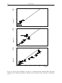
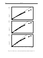
Simulated focal plane . . . . . . . . . . . . . . . . . . . . . . . . . . . . . . .
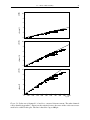
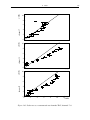
Exemplary electron trajectories for equidistant energies and scintillator bars . .
Exemplary electron trajectories for equidistant energies and adjusted positions
of the scintillator bars . . . . . . . . . . . . . . . . . . . . . . . . . . . . . . .
Exemplary electron trajectories for equidistant energies and adjusted positions
and widths of the scintillator bars . . . . . . . . . . . . . . . . . . . . . . . . .
Possibilities for multiple electron events . . . . . . . . . . . . . . . . . . . . .
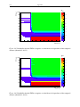
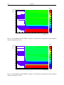
Staggering of the scintillator bars in multiple vertical planes . . . . . . . . . . .
Calculated detector layout with constant and variable resolution . . . . . . . . .
Resolution changeover in the vertical plane detector . . . . . . . . . . . . . . .
Simulated energy distribution and resolution without radiator and with Cu
200 µm radiator . . . . . . . . . . . . . . . . . . . . . . . . . . . . . . . . . .
Exploded view of the PMT assembly . . . . . . . . . . . . . . . . . . . . . . .
View of the back side of a slide . . . . . . . . . . . . . . . . . . . . . . . . . .
Profile of the slides for the prototype detector . . . . . . . . . . . . . . . . . .
Chassis with one mounted PMT assembly . . . . . . . . . . . . . . . . . . . .
Light guide . . . . . . . . . . . . . . . . . . . . . . . . . . . . . . . . . . . .
Assembly of the prototype detector . . . . . . . . . . . . . . . . . . . . . . . .
Block diagram of the electronics . . . . . . . . . . . . . . . . . . . . . . . . .
Simulated ADC spectrum of an ideal detector with two independent channels .
Passive pulse splitter . . . . . . . . . . . . . . . . . . . . . . . . . . . . . . .
Simulated TDC spectrum of an ideal detector with one channel . . . . . . . . .
View of the electronics setup used for the first test . . . . . . . . . . . . . . . .
Timing of the different signals. . . . . . . . . . . . . . . . . . . . . . . . . . .
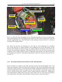
View of the framework in front of the CB tagging system . . . . . . . . . . . .
Top view of the CB tagging system . . . . . . . . . . . . . . . . . . . . . . . .
Measured ADC spectrum using channel 5 of the prototype detector during the
first test . . . . . . . . . . . . . . . . . . . . . . . . . . . . . . . . . . . . . .
Measured TDC spectrum using channel 5 of the prototype detector during the
first test . . . . . . . . . . . . . . . . . . . . . . . . . . . . . . . . . . . . . .
14
15
18
19
21
22
23
24
27
28
31
34
38
41
42
42
43
44
45
46
48
49
50
52
53
54
55
56
57
58
60
62
62
63
66
67
68
69
70
70
10
List of Figures
41
42
43
44
45
46
47
48
49
50
51
52
53
54
55
56
57
58
59
60
61
62
63
64
65
66
67
68
69
70
71
72
73
74
75
76
77
78
79
80
81
82
83
Measured TDC spectrum using channel 5 of the prototype detector during the
first test (detail) . . . . . . . . . . . . . . . . . . . . . . . . . . . . . . . . . . 71
Measured ADC spectrum using channel 5 of the prototype detector with entry
in TDC spectrum . . . . . . . . . . . . . . . . . . . . . . . . . . . . . . . . . 73
Threshold curve for channel 5 of the prototype detector . . . . . . . . . . . . . 73
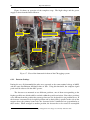
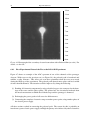
View of the prototype detector mounted in the BGO-OD area . . . . . . . . . . 74
Overview of the location for the BGO-OD tagging system and the electronics rack 75
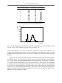
Photograph of the secondary electron beam taken with a Polaroid film . . . . . 76
Measured ADC spectrum using channel 5 of the prototype detector during the
second test . . . . . . . . . . . . . . . . . . . . . . . . . . . . . . . . . . . . . 77
Measured TDC spectrum using channel 5 of the prototype detector during the
second test . . . . . . . . . . . . . . . . . . . . . . . . . . . . . . . . . . . . . 78
Measured TDC spectrum using channel 5 of the prototype detector during the
second test (detail) . . . . . . . . . . . . . . . . . . . . . . . . . . . . . . . . 78
Simple efficiency measurement . . . . . . . . . . . . . . . . . . . . . . . . . . 80
Possible trajectories of electrons in the detector . . . . . . . . . . . . . . . . . 81
Effect of the dead time on coincidence counting . . . . . . . . . . . . . . . . . 82
Exclusive coincidences of each combination of two channels . . . . . . . . . . 83
Exclusive coincidences of each combination of two channels and channel 5 . . 83
ADC spectrum with fitted functions . . . . . . . . . . . . . . . . . . . . . . . 85
Pulse distortion in the ADC and the discriminator . . . . . . . . . . . . . . . . 86
Spill structure of the electron beam . . . . . . . . . . . . . . . . . . . . . . . . 90
Scaler rate of channels 1, 6 and 9 vs. extracted electron current . . . . . . . . . 91
Measurement of temporal distances . . . . . . . . . . . . . . . . . . . . . . . . 93
Scaler rate of channels 1, 6 and 9 vs. reconstructed rate from the TDC . . . . . 94
Scaler rate of channel 9 vs. scaler rate of channel 1 . . . . . . . . . . . . . . . 95
Counting of coincidences and timing . . . . . . . . . . . . . . . . . . . . . . . 96
Probability that the FPGA recognizes a coincidence . . . . . . . . . . . . . . . 97
Different types of accidental coincidences . . . . . . . . . . . . . . . . . . . . 98
Comparison of simulated and measured spectrum . . . . . . . . . . . . . . . . 100
Deviation of the simulated data from the measured data (CB) . . . . . . . . . . 101
Deviation of the simulated data from the measured data (BGO-OD) . . . . . . . 101
FrED board prototype . . . . . . . . . . . . . . . . . . . . . . . . . . . . . . . 105
Back plane of the chassis . . . . . . . . . . . . . . . . . . . . . . . . . . . . . 113
Left side plane of the chassis . . . . . . . . . . . . . . . . . . . . . . . . . . . 114
Right side plane of the chassis . . . . . . . . . . . . . . . . . . . . . . . . . . 115
Left side of the middle slide . . . . . . . . . . . . . . . . . . . . . . . . . . . . 116
Right side of the middle slide . . . . . . . . . . . . . . . . . . . . . . . . . . . 117
Left side of the top slide . . . . . . . . . . . . . . . . . . . . . . . . . . . . . . 118
Right side of the top slide . . . . . . . . . . . . . . . . . . . . . . . . . . . . . 119
Left side of the bottom slide . . . . . . . . . . . . . . . . . . . . . . . . . . . 120
Right side of the bottom slide . . . . . . . . . . . . . . . . . . . . . . . . . . . 121
Back side of the slides . . . . . . . . . . . . . . . . . . . . . . . . . . . . . . . 122
Clip used to fix the scintillator bars . . . . . . . . . . . . . . . . . . . . . . . . 122
Cylinder of the PMT assembly . . . . . . . . . . . . . . . . . . . . . . . . . . 123
Cap of the PMT assembly . . . . . . . . . . . . . . . . . . . . . . . . . . . . . 123
Part 1 of the cable lead through . . . . . . . . . . . . . . . . . . . . . . . . . . 124
Part 2 of the cable lead through . . . . . . . . . . . . . . . . . . . . . . . . . . 124
List of Figures
84
85
86
87
88
89
90
91
92
93
94
95
96
97
98
99
100
101
102
103
104
105
106
107
108
109
110
111
Clip used to fix the PMT assembly on the chassis . . . . . . . . . . . . . . . .
Light guide . . . . . . . . . . . . . . . . . . . . . . . . . . . . . . . . . . . .
Scintillator bar . . . . . . . . . . . . . . . . . . . . . . . . . . . . . . . . . . .
Framework used to mount the prototype detector behind the CB tagging system
Exclusive coincidences of two channels and channel 1 . . . . . . . . . . . . . .
Exclusive coincidences of two channels and channel 2 . . . . . . . . . . . . . .
Exclusive coincidences of two channels and channel 3 . . . . . . . . . . . . . .
Exclusive coincidences of two channels and channel 4 . . . . . . . . . . . . . .
Exclusive coincidences of two channels and channel 5 . . . . . . . . . . . . . .
Exclusive coincidences of two channels and channel 6 . . . . . . . . . . . . . .
Exclusive coincidences of two channels and channel 7 . . . . . . . . . . . . . .
Exclusive coincidences of two channels and channel 8 . . . . . . . . . . . . . .
Exclusive coincidences of two channels and channel 9 . . . . . . . . . . . . . .
Scaler rate vs. current in ELSA, channel 1–3 . . . . . . . . . . . . . . . . . . .
Scaler rate vs. current in ELSA, channel 4–6 . . . . . . . . . . . . . . . . . . .
Scaler rate vs. current in ELSA, channel 7–9 . . . . . . . . . . . . . . . . . . .
Scaler rate vs. reconstructed rate from the TDC, channels 1–3 . . . . . . . . . .
Scaler rate vs. reconstructed rate from the TDC, channels 4–6 . . . . . . . . . .
Scaler rate vs. reconstructed rate from the TDC, channels 7–9 . . . . . . . . . .
Scaler rate vs. scaler rate from the lowest channel, channels 7–9 . . . . . . . .
Probability that the FPGA recognizes a coincidence (channels 1 and 2) . . . . .
Probability that the FPGA recognizes a coincidence (channels 2 and 3) . . . . .
Probability that the FPGA recognizes a coincidence (channels 3 and 4) . . . . .
Probability that the FPGA recognizes a coincidence (channels 4 and 5) . . . . .
Probability that the FPGA recognizes a coincidence (channels 5 and 6) . . . . .
Probability that the FPGA recognizes a coincidence (channels 6 and 7) . . . . .
Probability that the FPGA recognizes a coincidence (channels 7 and 8) . . . . .
Probability that the FPGA recognizes a coincidence (channels 8 and 9) . . . . .
11
125
125
126
127
128
129
129
130
130
131
131
132
132
134
135
136
137
138
139
140
141
142
142
143
143
144
144
145
12
List of Figures
13
1
Introduction
“Measure what is measurable,
and make measurable what is not so.”
Galileo Galilei, 1564–1642
100 years ago, in 1910, Thomson proposed his atomic model in which the atom consisted
of an equally distributed mass and positive charge within which the electrons moved around
as particles. The charge of these electrons was shown to be opposite equal to the charge of a
singly ionised atom. The prior year, 1909, Geiger and Marsden had determined that α particles
impinging on a gold foil are scattered with angles larger than 90◦ . In 1911, Rutherford showed
that the observed rate of large angle scattering of α particles is inconsistent with Thomson’s
model. Instead, the mass of the atom has to be concentrated in a pointlike hard nucleus leading
to the cross section dσ ∼ sin−4 (θ /2), where θ is the scattering angle. Only two years later, in
1913, Bohr developed his model of the dynamics of the atom, incorporating quantum theory.
Using this model it was possible to predict discrete excited electron energy states which were
observed in the spectroscopy of hydrogen. About 50 years later, experiments done by Hofstadter
showed that the cross section for the elastic scattering of electrons off gold is smaller than
predicted for a pointlike nucleus. This led to the introduction of a form factor into the cross
section formula, describing the charge distribution of the nucleus. The inelastic scattering of
electrons off the nucleus showed that the nucleus can itself be excited and that it consists of
nucleons (protons and neutrons). It did not take long to discover that the nucleons also possess
excited states (like the ∆ resonance) and thus are not pointlike. Eventually the nucleons were
found to be made of two different quark flavours, the up and the down quark (today, four more
quark flavours are known: charm, strange, top and bottom). Beside nucleons, other baryons are
known, all made of three quarks. In addition to baryons, there are the mesons, consisting of one
quark and one anti-quark. The simplest mesons, made of up and down quarks, are the pions.
All quarks come in three different colour charges, which are charges of the strong interaction. This interaction is responsible for the binding of the nucleus, too, as it consists only of
positively charged protons and electrical neutral neutrons. Without the attractive force of the
strong interaction between nucleons to counterbalance the electromagnetic interaction, stable
nuclei could not exist. The strong interaction, however, differs from the electromagnetic interaction by an important fact: While the coupling strength αe of the electromagnetic interaction
decreases for larger distances, the coupling strength αs of the strong interaction increases. This
implies two phenomena: When looking at small distances (corresponding to a large momentum transfer Q2 ), the quarks inside the nucleons are quasi free, since αs ≪ 1. This behaviour
is called asymptotic freedom. In this region, the interaction of quarks is well understood and
described within perturbative QCD, the gauge theory of the colour interaction. For distances
about the size of the nucleons (small Q2 , αs > 1), the quarks are confined, making it impossible
to describe the excitation spectra of the nucleons within perturbative QCD. Various models have
been developed to describe the excitation spectra. Not all questions have been answered. E.g.,
the models predict that the number of predicted excited states is much larger than the number
of the observed states.
14
Introduction
.forw
ard s
.e −
pectr
o
mete
r
.
BGO
bal
1.8 m l
..
.taggin
g syst
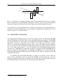
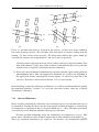
em
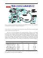
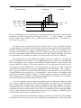
Figure 1. Overview of the BGO-Open Dipole experiment. The shown tagging detector belongs
to the old SAPHIR tagging system. Based on [Wal10].
To further examine the excitation spectra of the nucleons, the BGO-OD1 experiment (Figure 1) is currently set up at the electron stretcher accelerator ELSA in Bonn. It is funded by
the DFG2 within the Transregional Collaborative Research Centre 16: “Subnuclear Structure of
Matter”. To excite the nucleons, real photons of an energy of up to about 3 GeV are shot onto
a liquid hydrogen or deuterium target. The decay products of the excited states are detected in
a spectrometer, almost covering 4π of solid angle. The central detector, the BGO ball, is made
of 480 bismuth germanate (BGO)3 crystals. It can detect charged and uncharged particles. The
forward spectrometer consists of different detectors for charged particles and the spectrometer
magnet (the OD, open dipole). It is used to measure the tracks and the momenta of charged
particles emitted in forward direction. The photons are produced in the tagging system, using
the high energetic electron beam of ELSA. Figure 2 shows an overview of the electron accelerator. Unpolarised and polarised electrons are produced in the LINAC1 and LINAC2 respectively.
They are then accelerated in the booster synchroton and the subsequent stretcher ring to a maximum energy of E0 = 3.5 GeV. The beam can then be extracted to the BGO-OD or Crystal
Barrel (CB) experiment.
Among different experiments studying similar questions, two different tagging methods
are used: the Bremsstrahlung tagging and the Compton backscattering technique. For the BGOOD experiment, Bremsstrahlung tagging is used. By shooting electrons onto a thin (about
100 µm) radiator, they are scattered and lose energy in the form of photons. The energy of the
photons can be inferred through the detection of the electrons in a magnetic spectrometer. Table
1 shows an overview of different similar experiments, their tagging method, maximum photon
1 BGO
= Bismuth germanate, OD= Open Dipole
ForschungsGemeinschaft (German Research Foundation)
3 Bi Ge O
4
3 12
2 Deutsche
15
.
.BGO-OD
.
.
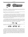
Figure 2. Overview of the Electron Stretcher Accelerator (ELSA) [els10a]. Some components
of the BGO-OD experiment are missing in this picture.
energy, photon rate, and the tagged range of the photon energy. The concept of photon tagging
will be described in detail in Chapter 2.4.
This thesis covers the development of the tagging hodoscope. This part of the tagging
system detects the electrons which were scattered during the Bremsstrahlung process. The
focus of the study is primarily on the part which detects high energetic electrons and is exposed
to the highest rates. The readout electronics is developed in [Mes10]. The Bremsstrahlung
target is part of [Bel10]. After describing the basics in Chapter 2, the requirements for the new
tagging system are defined in Chapter 3. Based on the requirements, the general design for the
detector is developed in Chapter 4. The building of a small prototype is described in chapter 5.
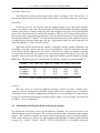
Experiment
Method
CLAS (JLab) [FP09a]
Brems.
SAPHIR (ELSA) [SBB+ 94] Brems.
CB (ELSA) [CMA+ 09]
Brems.
LEPS (SPring-8) [lep10]
Compton
GRAAL (ESRF) [BAA+ 97] Compton
A2 (MAMI C) [MKA+ 08]
Brems.
MAX-Lab [O’R10, Bru10]
Brems.
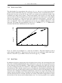
Eγ , max /GeV
nγ /s−1 MeV−1
Eγ /Eγ , max /%
6.0
2.8
3.2
2.4
1.7
1.5
2.0
104
103
104
103
103
105
105
20–95
32–93
9–91
60–100
33–100
5–93
6–90
Table 1. Properties of different photon tagging systems. nγ is the approximate photon rate. See
also [FP09a] for all entries except for MAX-Lab.
16
Introduction
The in beam testing is presented in Chapter 6. Chapter 7 covers the analysis of the experimental
data. Finally, a short summary is given in chapter 8, followed by a conclusion.
17
2
Basics of the Underlying Physical Processes
2.1
System of Units and Symbols
Throughout this work, the natural system of units will be used, which is defined by
h̄ = c = 1.
(1)
Especially during theoretical calculations, also
me = 1
(2)
to further simplify complex expressions. When using only the equivalence h̄ = c = 1,
[energy] = [momentum] = [mass] = [length]−1 = [time]−1
(MeV units).
(3)
When also using me = 1,
[energy] = [momentum] = [mass] = [length] = [time] = 1.
(4)
The following symbols will be used in this section:
E0 , p0 = initial energy and momentum of the electron
E, p = energy and momentum of the scattered electron
k, k = energy and momentum of the emitted photon
β0 , β = velocity of incident and scattered electron; unless otherwise quoted, β0 ≃ β ≃ 1
θ0 , θ = angles of p0 and p with respect to k
ϕ = angle between the planes (p0 , k) and (p, k)
dΩk = element of solid angle sin θ0 dθ0 dϕ in the direction of k
dΩ p = element of solid angle sin θ dθ dϕ in the direction of p
q = momentum transferred to the nucleus, q = p0 − p − k
θMS = RMS of the angle for multiple scattering projected onto a plane
X0 = radiation length (for copper, X0 = 1.42 cm)
α = Fine structure constant, α ≃ 1/137
2.2
Bremsstrahlung
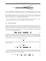
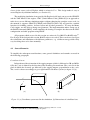
The process which is responsible for the emission of photons when electrons travel through
material is called Bremsstrahlung. When an electron of momentum p0 traverses the Coulomb
field of a nucleus, there is a certain chance for it to be scattered, leading to the radiation of a
photon of momentum k (see Figure 3). The nucleus is needed to take the recoil momentum
q. Otherwise, this process would be kinematically impossible due to momentum and energy
conservation. Only the incoherent Bremsstrahlung will be discussed here. In the coherent
Bremsstrahlung process, the electrons are scattered in a crystal. The recoil momentum is then
absorbed by the lattice, just as in the Mößbauer effect (see e.g. [Sie76]). The process of coherent
18
Basics of the Underlying Physical Processes
.nucleus
.
.e, p0 , β .
.θ
.θ0
.γ , k
.e, p
Figure 3. Kinematics of the Bremsstrahlung process. The incoming electron is scattered in the
electric field of the nucleus. During the scattering process, a Bremsstrahlung photon is emitted.
Bremsstrahlung strongly depends on the orientation of the momentum transfer q with respect
to the reciprocal lattice of the crystal. This technique can be used to produce linear polarised
photons (for more details, see e.g. [EBB+ 09, Tim69, Bel10]).
It is not useful to derive the complete quantum mechanical cross section here. A more
qualitative approach will be used (see e.g. [Gre00], more details in [Jac06]).
2.2.1 Energy Distribution
Instead of viewing the electrons as incident on some material, they will be considered at rest,
while the nuclei of the target material are considered to be moving with high velocity in the
direction of the electrons. The electromagnetic field of the moving nuclei can be handled as
a distribution of low energy photons, given by the Weizsäcker Williams distribution [Jac06]
(me = 1, as in all following calculations):
[ (
)
]
dNγ (k) 2α 1 1
2 · 1.123 E β 2
β2
≃
ln
−
.
(5)
dk
π β2 k
k
2
The nuclei have Z protons. Since the photons are soft, their phase does not change significantly
within the size of the nuclei. Therefore, the amplitudes for each proton can be added coherently,
leading to factor of Z 2 for the total cross section. The cross section for the scattering of a single
(soft) photon off the electron is the Thomson cross section
σT =
8π 2
α .
3
(6)
The Bremsstrahlung cross section is then the product of the photon distribution and the Thomson cross section:
dNγ
d σk ≃ Z 2
σT dk,
[ ( dk
)
]
16 2 3 dk
2 · 1.123 E β 2
β2
dσk ≃ Z α
ln
−
.
3
k
k
2
(7)
(8)
The quantum mechanical approach in the Born approximation uses the Feynman diagrams
of Figure 4. It results in the following for the cross section differential in the photon energy
(extreme relativistic case, E0 , E, k ≫ 1) [KM59]:
[
][ (
( )2
)
]
2
dk
E
E
2EE0
1
2 3
−
1+
ln
− .
(9)
dσk = 4Z α
k
E0
3 E0
k
2
2.2
Bremsstrahlung
19
.γ
.γ
e..
.e
.e
.e
.
.
.Z
.Z
Figure 4. Feynman graphs for Bremsstrahlung.
Thus, the simple approach is very close to the more exact quantum mechanical derivation.
Since the exact shape is not needed for the present work, the energy distribution will mostly be
approximated by
d σk ∼
dk
.
k
(10)
2.2.2 Angular Distribution
The formula for the cross section, which is differential in photon and electron emission angles,
is given in [KM59]:
dσk,θ0 ,θ ,ϕ
{
)
p2 sin2 θ ( 2
Z 2 α 3 dk p dΩk dΩ p
2
=
4E
−
q
0
4π 2 k p0
q4
(E − p cos θ )2
(
)
2
( 2
)
2pp
sin
θ
sin
θ
cos
ϕ
4EE
−
q
p20 sin2 θ0
0
0
0
+
4E − q2 −
(E0 − p0 cos θ0 )2
(E − p cos θ )(E0 − p0 cos θ0 )
(
)}
2k2 p2 sin2 θ + p20 sin2 θ0 − 2pp0 sin θ sin θ0 cos ϕ
+
,
(E − p cos θ )(E0 − p0 cos θ0 )
(11)
q2 = p2 + p20 + k2 − 2p0 k cos θ0 + 2pk cos θ − 2p0 p(cos θ cos θ0 + sin θ sin θ0 cos ϕ ).
(12)
Using this as a starting point, it can be derived [BLP71] that the photon and the secondary
electron move forwards in a narrow cone with an apex angle
δ≃
1
,
E0
(13)
also called the characteristic angle. For a beam energy of E0 = 3200 MeV, this means
δ ≃ 0.16 mrad.
(14)
20
Basics of the Underlying Physical Processes
2.2.3 Limitations of the Born Approximation
The Born approximation requires that the kinetic energies of the initial and final electron are
large enough to fulfil [KM59]
2π Z α
≪ 1,
β0
2π Z α
≪ 1.
β
(15)
For β0 ≃ β ≃ 1 and a radiator made of copper (Z = 26), 2π Z α /β = 1.33. Consequently, this
approximation can be expected to deviate from the exact behaviour by a small amount.
For extreme relativistic energies, the screening of the field of the nucleus by the electrons
of the atomic shell has to be taken into account. Using the atomic form factor
(
)
∫
sin qr 2
4π
F(q, Z) =
ρ (r)
r dr,
(16)
Ze
qr
where ρ (r) is the electron charge distribution, the cross section formulas 9 and 11 can be corrected by simply multiplying dσ by [1 − F]2 . Using a Thomas-Fermi model for the atom, the
amount of screening can be expressed in terms of γ , defined as
γ=
100k
1
.
(17)
E0 EZ 3
This number is close to the ratio of the radius of the atom ra ≃ 1/(α Z 1/3 ) and the maximum
−1 ≃ 2E E/k. If
impact parameter, which for relativistic energies, is rmax = q−1
0
min = (p0 − p − k)
the maximum impact parameter is much larger than the radius of the atom (γ ≃ 0), the charge
of the nucleus is completely screened. If it it close to the radius of the nucleus (γ ≫ 0), the
complete charge Ze is seen by the electron. Assuming an incident electron energy of E0 =
3200 MeV and 5 %E0 < k, E < 95 %E0 , it follows that 3 × 10⁻⁴ < γ < 0.01, corresponding to
almost complete screening. In this case, the cross section may be approximated by [KM59]
{[
]
}
( )2
(
) 1E
E
2E
2 3 dk
− 31
dσk = 4Z α
ln 183Z
+
.
(18)
1+
−
k
E0
3 E0
9 E0
2.3
Multiple Scattering
The main process responsible for deflections of incident electrons is multiple scattering. It is
caused by many small angle scattering processes, mainly in the Coulomb field of the nuclei. Neglecting few large angle deflections, the angular distribution may be approximated as Gaussian
with an RMS value which is given by [LD91]:
( )]
√ [
x
13.6 MeV x
1 + 0.038 ln
.
(19)
θMS =
p0
X0
X0
θMS is the RMS deflection angle
√ of the scattering projected to a plane. The RMS angle in
space
the space is given by θMS = 2θMS . Here, x/X0 is the thickness of the scattering medium
measured in radiation lengths.
2.4 Principle of Photon Tagging
21
.ϑ2
.ϑ
.e, E0 , β .
.ϑ1
.γ , k
.e, E
.γ , k0
Figure 5. Kinematics of the Compton backscattering process.
2.4
Principle of Photon Tagging
As already pointed out in Section 1, there are mainly two different methods for producing highly
energetic photon beams: Bremsstrahlung tagging and Compton backscattering. Both methods
make use of a scattering process with accelerated electrons and for both, the scattered electron is
momentum analysed to infer the photon energy and the time of production, i.e. tag the photon.
The two methods are presented next in general terms. Then, the method of Bremsstrahlung
tagging is described in more detail.
2.4.1 Methods of Photon Production
Compton Backscattering
It is possible to produce a beam of high energy photons by Compton scattering laser light
against highly energetic electrons, e.g. those produced in a storage ring [BAA+ 97, BCD+ 90].
When laser light with energy k0 is incident on the electron beam at an angle of about ϑ1 ≃ 180◦ ,
it is scattered backwards close to the direction of the incoming electrons. Using ϑ2 as the angle
of the scattered photon with respect to the incoming photon beam, and ϑ as the angle of the
scattered photons with respect to the electron beam (see Figure 5), the energy k of the scattered
photon is [DBB+ 00]:
k = k0
1 − β cos ϑ1
.
1 − β cos ϑ + (k0 /E0 )(1 − cos ϑ2 )
(20)
In the extreme relativistic case, β ≃ 1, E0 ≫ 1, ϑ1 ≃ ϑ2 ≃ 180◦ , ϑ ≪ 1, equation 20 can be
approximated as
k=
4E02 k0
.
1 + 4E0 k0 + (E0 ϑ )2
(21)
The energy of the scattered photon is highly dependent on the emission angle. When collimating the photon beam, it is still necessary to use a tagging method to obtain the photon energy
exactly. For Compton backscattered photons, two tagging methods exist: internal and external.
For internal tagging, the scattered electrons are momentum analysed by the magnets of the storage ring. The detectors are located very close to the main orbit of the storage ring. For external
tagging, the scattered electrons are removed from the storage ring by an additional magnetic
field and are analysed by an external tagging spectrometer, similar to the Bremsstrahlung tagging.
22
Basics of the Underlying Physical Processes
.
dipole
magnet.
.
tagging .
detector interaction
zone
.laser
..
Figure 6. Layout of the GRAAL beamline [BAA+ 97].
The method of internal tagging is e.g. used in the GRAAL4 experiment at the ESRF5
in Grenoble [BAA+ 97] (see Figure 6). An argon laser produces photons with wavelengths of
351 nm and 514 nm. The laser photons interact with the electron beam between two bending
magnets over a distance of 6.5 m. During the backscattering on the E0 = 6 GeV electrons, the
photons acquire a maximum energy of kmax = 1.5 GeV. The scattered electrons are deflected by
the bending magnet and are separated by at most 56 mm from the electron beam. The detector
for the scattered electrons is located directly after the bending magnet, at a minimum distance
of 14 mm to the beam.
Bremsstrahlung Tagging
With Bremsstrahlung tagging, the electron impinges on a thin (about 100 µm) radiator
foil made of a high Z material, e.g., copper. The electrons emit Bremsstrahlung radiation with a
certain probability when traversing this foil and are then guided into the spectrometer magnet.
Their deflection in the magnetic field depends on their energy loss during the Bremsstrahlung
process. By detecting the electrons spatially resolved in the tagging spectrometer, their energy
and thus the energy of the photons can be deduced.
There are three main differences of the photon spectra between the two methods:
(1) It is apparent from Table 1 that the photon rates achieved with Bremsstrahlung tagging are
(at the present state) much higher (105 s−1 MeV−1 ) than the rates achieved with Compton
backscattering (103 s−1 MeV−1 ).
(2) With Compton backscattering, is it easily possible to produce highly polarised photon
beams. When using linear or circularly polarised laser light, the backscattered photon are
also linear or circularly polarised. The degree of polarisation can be up to 100 % for the
maximum photon energy. The maximum polarisation is in principle only limited by the
polarisation of the laser beam [BAA+ 97].
To produce polarized photons with a Bremsstrahlung tagging system, coherent Bremsstrahlung is used. Instead of an amorphous radiator like copper, a crystal, e.g. diamond,
4 GRenoble
5 European
Anneau Accèlèrateur Laser
Synchrotron Radiation Facility
2.4 Principle of Photon Tagging
23
has to be used and precisely aligned with respect to the beam direction [EBB+ 09]. For
present experiments, the maximum degree of polarisation that can be reached is about
80 %.
(3) The energy spectrum of Compton backscattered photons is rather flat, compared to the
dNγ ∼ dEγ /Eγ shape of the Bremsstrahlung spectrum. By collimating the photon beam,
low energy photons can be removed, resulting in a high energy photon beam.
For the BGO-OD experiment, the Bremsstrahlung method will be used. This method proved to
work fine for all other experiments which are/were run at ELSA (e.g. CB [FP09a] and SAPHIR
[Bur96]) and provides the highest photon rates. In order to switch to Compton backscattering,
the acceleration facility would have to be modified, which would raise the expenses by an
unacceptable amount.
2.4.2 Elements of a Bremsstrahlung Tagging System
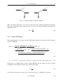
The complete tagging system6 consists of three distinct parts: the radiator, the tagging magnet,
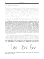
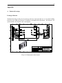
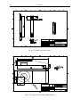
and the tagging hodoscope. A schematic of such a tagging system is shown in figure 7. The
primary electron beam enters from the left and hits the radiator. Some electrons will undergo
Bremsstrahlung and lose a varying amount of energy which depends on the cross section (see
Section 2.2). The scattered electrons as well as the remaining primary beam are then deflected
by the tagging magnet into the tagging hodoscope and the beam dump, respectively. Usually,
the tagging magnet is simply a dipole magnet. The beam dump does not belong directly to
the tagging system but is needed to stop the primary beam. For more information on the beam
dump, see e.g. [Els07].
.radiator
.
.tagging magnet
.
.γ
.primary
beam
tte
.sca
.beam dump
red
−
e
.
ope
c
s
odo
.h
Figure 7. General scheme of a Bremsstrahlung tagging system. For a description, see the text.
6 from
this point, when referring to tagging system, it is always meant a Bremsstrahlung tagging system
24
Basics of the Underlying Physical Processes
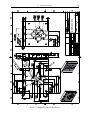
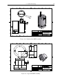
.beam
.wire7
.Cu 50 µm
.Cu 100 µm
.wire
.Cu 200 µm
..
.screen8
.
.(a)
.(b)
.Kapton 125 µm
Figure 8. The Goniometer (a) and the different radiators (b). The bottom and the middle stage
move perpendicular to the beam direction (horizontal and vertical). The top stage rotates the
plate around the beam axis, the other two stages rotate it perpendicular to the beam axis. The
radiator plate is mounted back to back onto the goniometer .
The Radiator
First, the electron beam hits the radiator. During their transit through the material, the
electrons undergo Bremsstrahlung with a certain probability, resulting in a specific energetic
and angular distribution (see Section 2.2). For the BGO-OD experiment, multiple different
radiators and parts for beam diagnostics are mounted on a round plate sitting on a goniometer.
A goniometer is an instrument consisting of different motorised stages, allowing for a precise
positioning and alignment of the radiator plate in multiple dimensions. The high precision
is mainly needed for the alignment of a diamond which is used for coherent Bremsstrahlung.
Currently, a new goniometer (Figure 8 (a)), consisting of two linear and three rotation stages is
installed [Bel10]. Figure 8 (b) shows the plate with the different radiators. The indicated beam
direction corresponds to the use of the diamond radiator. Otherwise, one of the other radiators
can be moved into the beam by the bottom linear stage and the top rotation stage.
Three different copper radiators (50 µm, 100 µm and 200 µm) will be used to generate incoherent Bremsstrahlung. Their thickness, measured in radiation lengths, is x/X0 =
3.5 × 10⁻³ , 7.0 × 10⁻³ and 14.0 × 10⁻³ . Horizontal and vertical wires are used to measure the
profile of the electron beam. By moving them through the beam and measuring the rate of
Bremsstrahlung electrons, the beam structure can be inferred. With the aid of the luminescent
Chromox screen, the electron beam can be directly observed. In the centre hole, the diamond
will be mounted.
7 used
for beam scans
screen for an optical inspection of the beam
8 Chromox
2.4 Principle of Photon Tagging
25
The Tagging Magnet
The scattered electrons are vertically deflected in the magnetic field of the tagging magnet.
The BGO-OD experiment uses a magnet identical to the one used in the CB experiment. It is a
dipole magnet from Brown-Bovery Switzerland (type MC). It can be operated with currents up
to 1500 A, corresponding to a maximum field value of B = 2.0 T.
For each beam energy, the current in the magnet is adjusted in a way that the primary
electron beam is always deflected by the same angle to enter the beam dump. For BGO-OD,
this angle is αtag = 7.8◦9 , for CB, this angle is αtag = 9.0◦ [FP09a]. The effect of a constant
magnetic field on relativistic particles is given by
dv √
B
= αv × .
(22)
dt
E0
This expression depends only on the ratio B/E0 . As long as the magnetic field increases linearly
with the current, the required current is proportional to the energy of the primary electron beam.
For currents of up to 800 A, the deviation from the linear behaviour is smaller than 1 % [FP09a].
The field map of the CB tagging magnet has been measured for five different energies
of the primary electron beam [Bal10]. Since the BGO-OD tagging magnet is operated with a
lower magnetic field for the same energies, the field map has to be scaled accordingly using
the ratio of the currents in the two magnets. This is possible at least for beam energies up to
E0 = 2400 MeV, because the currents are then smaller than 700 A. This is discussed in more
detail in Section 4.3.
Another important feature of a dipole magnet (like the tagging magnet) is its focussing
ability. Electrons which do not enter the magnet at a central axis, the z-axis, are deflected
towards this axis. Hence, the magnet acts like a lens on the electron beam. One reason for this
focussing is the fringe field of the magnet. The magnetic field inside of the magnet is almost
constant in a certain range. Outside of this range, it ramps down to zero over a characteristic
distance. In the absence of sources (electric currents) the following equations holds:
∇ × B = 0,
∇ · B = 0.
(23)
Hence, the change of one component of the magnetic field induces also a change of the other
components. If the field B0 inside of the magnet points into the y-direction, there are also finite
contributions to the x and z components at the exits of the magnet [Gre00]:
(
)
Bx ∼ −xy ∂z2 By
(24)
Bz ∼ y (∂z By )
(25)
The fringe fields Bx and Bz vanish at the centre axis and focus electrons of the same energy into
a small spot, the focal point (for more details, see [Gre00]). The plane consisting of the focal
points for different electron energies is the focal plane. It will be calculated in Section 4.4.
The Tagging Hodoscope
Finally, the scattered and deflected electrons enter the tagging hodoscope. From the detected position one obtains the scattered electron’s energy and thus the Bremsstrahlung photon
9 this
number is calculated from the simulation, see also Section 4.3
26
Basics of the Underlying Physical Processes
energy, given the primary electron energy. It is obvious that the placement of the hodoscope
into the focal plane of the tagging magnet increases the energy resolution. There are different
possible detectors to detect the deflected electrons:
(1) Scintillation counters using plastic scintillator and photomultiplier tubes offer a fast and
precise measurement of the timing of incoming electrons. Plastic scintillators can have a
rise time of about 0.5 ns, photomultiplier tubes have a transit time of some ns and a jitter
of ∆t ≃ 0.5 ns [Leo94]. It is easily possible to manufacture plastic scintillator bars in the
desired sizes down to certain limit, given by the size of the PMTs and the required light
output.
(2) In contrast to scintillation counters, MWPCs10 offer a high spatial resolution of 100 µm
and smaller [Gre00]. However, the timing resolution is not suitable to be used as reference. Assume a wire spacing of 2 mm and a drift velocity of 10 cm µs−1 . Then, the time
between the transit of the electron and the arrival of the ionisation electrons at the anode,
where most of the gas amplification takes place, can differ by ∆t ≃ 1 mm/10 cm µs−1 =
10 ns ≫ ∆tPMT . It is, however, possible to use a MWPC and scintillation counter together
and measure position and time separately. This method was used for the SAPHIR tagging
system TOPAS II [Bur96].
(3) Detectors making use of Čerenkov radiation are very fast, since the light is emitted almost
instantaneously when the electron traverses the material. This light can be detected using
PMTs. The downside is that these detectors have to be rather big to maintain a sufficient
light output, which strongly affects the spatial resolution. A lead glass Čerenkov detector
is for example employed in the CB Møller Polarimeter [Kam10].
For the BGO-OD tagging system, the first method is chosen. The use of a combined system of
an MWPC and large scintillator bars limits the maximum electron rate which can be detected,
because each single PMT sees a substantial fraction of the total rate and the MWPC already
saturates at small rates. When using smaller scintillator bars, the total rate can be increased.
At the same time, the spatial resolution of the scintillator bars can be improved sufficiently, so
no additional position resolving detector is needed. A positive side effect is the lower cost of
a single detector compared to a combined system. To further increase the resolution at the low
photon energy limit, one can think of an additional scintillating fibre detector as used for the
CB tagging system [FP09a].
2.5
Detector Components
The functionality of plastic scintillator and photomultiplier tubes (PMTs) is explained in more
detail in this section.
2.5 Detector Components
27
Figure 9. Energy level diagram of an organic scintillator molecule [Leo94].
2.5.1 Scintillators
A plastic scintillator is actually an organic scintillator dissolved in a plastic solvent. Common
solvents are PS11 and PVT12 .
A charged particle traversing through plastic scintillation material deposits ionisation energy in the solvent. This energy is transferred very quickly to the actual scintillator, e.g. pTerphenyl13 , PBD14 and PBO15 . The scintillator gets excited to a triplet state (T∗ , T∗∗ , . . . ) or
to a singlet state (S∗ , S∗∗ , . . . ) (see Figure 9). These states all decay to the S∗ state via internal
degradation, without emitting radiation. The S∗ state decays radiatively with a high probability
to a vibrational state of S0 . Since the energy of the radiated photon is smaller than the distance
between S0 and S∗ , the scintillator is transparent to its own radiation. Usually, a secondary
scintillator like POPOP16 is added to shift the wavelength of the radiation to a more suitable
value in the visible range (about 420 nm [Gre00]).
The light output of a scintillation material, i.e. the number of emitted photons, is typically
measured relative to the light output of anthracene (an organic crystal). In anthracene, an electron loses in average εant ≃ 60 eV per emitted photon. The light output of plastic scintillators
lies around 60 % of anthracene, so that εpl ≃ 100 eV [Leo94].
2.5.2 Photomultiplier Tubes
A photomultiplier tube (PMT) is a device which is able to convert very faint light pulses (down
to single photons) into an electric signal. A simple layout is shown in Figure 10. After the
photons pass through the input window (faceplate), they hit the photocathode. Due to the photoelectric effect, photoelectrons are emitted. The probability for a single photon to produce
10 Multi
Wire Proportional Chambers
trichloro(nitro)methane, CCl3 NO2 [che10]
12 PolyvinylToluene, 1-ethenyl-2-methylbenzene; 1-ethenyl-3-methylbenzene; 1-ethenyl-4-methylbenzene,
C27 H30 [che10]
13 1,4-di(phenyl)benzene, C H [che10]
18 14
14 2-phenyl-5-(4-phenylphenyl)-1,3,4-oxadiazole, C H N O [che10]
20 14 2
15 1-pyridin-3-ylbutan-1-on, C H NO [che10]
9 11
16 5-phenyl-2-[4-(5-phenyl-1,3-oxazol-2-yl)phenyl]-1,3-oxazole, C H N O [che10]
24 16 2 2
11 PolyStyrene,
A photomultiplier tube is a vacuum tube consisting of an input window, a
photocathode, focusing
electrodes,
an electron Physical
multiplierProcesses
and an anode usuBasics
of the Underlying
ally sealed into an evacuated glass tube. Figure 2-1 shows the schematic
construction of a photomultiplier tube.
28
FOCUSING ELECTRODE
SECONDARY
ELECTRON
DIRECTION
OF LIGHT
LAST DYNODE
STEM PIN
VACUUM
(~10P-4)
e-
FACEPLATE
STEM
ELECTRON MULTIPLIER
(DYNODES)
ANODE
PHOTOCATHODE
THBV3_0201EA
Figure 2-1: Construction of a photomultiplier tube
Light which
a photomultiplier
tube is detected andTubes
produces
an
Figure
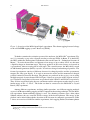
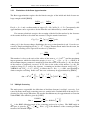
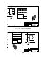
10.enters
Construction
of a Photomultiplier
[Ham07].
output signal through the following processes.
(1) Light passes through the input window.
(2) Light excites the electrons in the photocathode so that photoelecan electron is calledtrons
theare
quantum
efficiency.
quantum
efficiency
emitted into
the vacuum The
(external
photoelectric
effect). depends strongly on its
Photoelectrons
are accelerated
andisfocused
by the
focusing
elec-Next, dynodes are conwavelength. The(3)
maximum
quantum
efficiency
typically
about
25 %.
trode
onto
the
first
dynode
where
they
are
multiplied
by
means
of the flight path of the
nected to different high voltages in a way that the voltage increases along
secondary electron emission. This secondary emission is repeated
electrons. This way, the electrons from the photocathode are accelerated until they hit the first
at each of the successive dynodes.
dynode and produce
more free electrons. This is repeated several times, until the electrons are
(4) The multiplied secondary electrons emitted from the last dynode are
collected at the anode.
The
total gain
multiplication of the PMT is the number of output elecfinally
collected
by theor
anode.
trons divided by the number of photons. Gains of about 107 can be achieved. There are other
This chapter describes the principles of photoelectron emission, electron trakinds of dynode
layouts, but the amplification principle is the same for all PMTs. Because the
jectory, and the design and function of electron multipliers. The electron multigain depends strongly
the focussing
ofare
theclassified
electrons
onto
thenormal
dynodes,
already weak magpliers used on
for photomultiplier
tubes
into two
types:
disnetic field can crete
leaddynodes
to a decrease
ofmultiple
gain by
distorting
the dynodes
flight path
the electrons. To shield
consisting of
stages
and continuous
such asofmiSince both
types aof layer
dynodesof
differ
considerably
in operating
the PMT from crochannel
externalplates.
magnetic
fields,
high
permeable
metal, e.g. Mumetal17 , can
principle,
tubes using microchannel
plates (MCP-PMTs)
are itself and exceed the
be wrapped about
the photomultiplier
tube. This shielding
should be longer
as the PMT
separately described in Chapter 10. Furthermore, electron multipliers for variphotocathode by
at least the radius of the shielding [Ham07].
ous particle beams and ion detectors are discussed in Chapter 12.
The dynode voltages are usually obtained with a simple voltage divider circuit which is
© 2007 HAMAMATSU PHOTONICS K. K.
connected to a single high voltage source (about 0.5 kV–2 kV). The combination of the socket
which holds the PMT and the voltage divider is called a socket assembly. It has at least two
connections, the high voltage input and the signal output.
2.5.3 Light Collection and Efficiency
Because the shape of the scintillator generally differs from the shape of the PMT window, they
cannot be connected together directly. Instead, a light guide, often made of PMMA18 , is put
between them. If properly designed, the light is totally reflected inside of the light guide with
the result that the light is efficiently transferred from the scintillator to the PMT. The critical
angle θc for total reflection has to be kept in mind when designing the shape of such a light
guide. If a kink exist that has a smaller angle than θc , some photons will escape the light guide.
17 a
nickel-iron alloy with a very high magnetic permeability µ > 50000
methacrylate), e.g. “Plexiglas”
18 Poly(methyl
2.5 Detector Components
29
The efficiency of a complete scintillation counter (PMT and scintillator bar) is determined
by the number of electrons that finally reach the anode of the PMT. The efficiency depends on
different parameters of all three components. This is illustrated in the following example. The
density of a plastic scintillator is roughly ρ = 1 g/cm3 . For a scintillator thickness of x = 0.5 cm,
the mean energy deposit of a minimum ionising particle (MIP) is ∆E = 2 MeVg/cm2 · xρ =
1 MeV, corresponding to 104 scintillation photons (ε = 100 eV). Because the light is emitted
isotropically, only a fraction of the photons are emitted in a direction that is totally reflected.
This fraction is
∫ 2π
∫ 90◦ −θc
∆Ω
1
dθ sin θ = (1 − sin θc ) ≃ 0.2,
=
dϕ
(26)
4π
2
0
0
for plastic with θc = 39◦ . Further photons are lost in the light guide if the cross section of the
scintillator bar A is bigger than the cross section of the area A′ which is coupled to the PMT.
Then, at most A′ /A photons are transmitted [Leo94]. For a scintillator width of 2 cm (the thickness is 0.5 cm) and a diameter of the photo cathode of 8 mm, the ratio A′ /A is approximately 0.5,
and about 104 · 0.2 · 0.5 = 1000 photons will reach the PMT. With a mean quantum efficiency
of ∼ 10 %, about 100 electrons will be released in the photocathode. This number fluctuates
statistically, but the probability that none or only a few electrons are produced is close to zero.
Hence, in most cases a detectable electric signal will be generated, implying an efficiency of
the scintillation counter close to 100 %.
In this example, the loss of light in the coupling between light guide and scintillator and
PMT respectively was neglected. For wavelengths larger than 350 nm the transmission of different cyanoacrylate glues and silicone is close to 100 %, so in most cases no light is lost [Leb02].
More photons can however be lost if the emission spectrum of the scintillator and the transmission spectrum of light guide and the window of the PMT do not match up. Furthermore, a
flawed, or non polished surface of the scintillator and the light guide, as well as air between the
different components (e.g. in the glue film), leads to additional losses, which potentially lead to
an efficiency smaller than 100 %. Moreover, electrons which hit only an edge of the scintillator
will produce less photons in the first place and are detected with a lower efficiency.
30
Basics of the Underlying Physical Processes
31
3
Requirements of the BGO-OD Tagging System
Several aspects have to be considered when designing the tagging system for the BGO-OD
experiment. The experiment itself makes demands on the energy resolution and the precision
of the timing. An additional emphasis is placed on a straightforward and easily maintainable
system, as the tagging system has to be always completely ready for operation. The largest
constraint for the detector design is the spatial situation. Only a limited amount of space is
available between the tagging magnet and the beam dump.
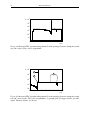
3.1
Spatial Restrictions
The arrangement of the tagging magnet and the beam dump could only be changed by a major
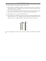
rebuilding of the experimental site and therefore provides a fixed restriction for the design of
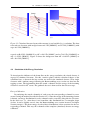
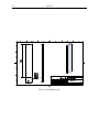
the tagging system. Figure 11 shows a drawing of the tagging magnet and the beam dump, the
latter constituting the main spatial restriction. The magnet is oriented in a way such that the
electrons entering from the left are deflected towards the ground. As explained in Section 4.4,
its focal plane is almost parallel to the bottom side and lies closely below it. That implies that
the focal points for high energetic electrons lie within the beam dump or even beyond, so that
only a part of the tagging hodoscope can be placed into the focal plane. The remaining part
has to be located in front of the beam dump, above the focal plane. Electrons which lost only
a small amount of energy during the Bremsstrahlung process will be very close to the primary
beam at this distance to the magnet, as both the scattered electrons and the primary beam are
deflected by nearly the same angle.
.beam
..
Figure 11. Side view of the available space for the tagging system. The electron beam enters
from the left. Distances are given in mm (scale 1:50). Based on [Wal10].
32
3.2
Requirements of the BGO-OD Tagging System
Energy Range and Resolution
Ideally, the tagged energy range should be as large as possible to cover a maximum photon
energy range for a single energy of the primary beam. It is still possible to deactivate single
channels when a higher amount of high energetic photons is needed and the extracted electron
current is increased. The channels for the low energetic photons may then saturate due to the
larger rate (dσ ∼ dEγ /Eγ ) and therefore are not used in this case.
At the small electron energy end, the range is limited by the dimensions of the magnet.
Very low energetic electrons are deflected so strongly that they do not leave the magnet and
cannot be detected. At the high electron energy end, the range is limited due to the primary
beam. The primary beam must not hit the hodoscope under any circumstances, but has to fly
into the beam dump. If it hits parts of the detector, it will illuminate the complete system due
to the large amount of multiple scattering, simply because of the huge intensity compared to
the electrons which underwent Bremsstrahlung. To maximise the range towards this end, the
mechanical construction should not exceed the detector channel which is closest to the primary
beam.
Besides other factors, e.g. the condition of the primary beam, the energy resolution of the
hodoscope is limited by the physical width of the scintillator bars. The smaller the bars are, the
better is the spatial resolution and thus the energy resolution. The energy width ∆Eγ is defined as
the span which is covered by one detector channel, so that photons between Eγ ± ∆Eγ /2 cannot
be distinguished. For a beam energy of E0 = 3200 MeV, an energy width between 20 MeV
(0.6 %E0 ) and 50 MeV (1.5 %E0 ) is targeted. The actual resolution σEγ is different from ∆Eγ
and does not only depend on geometrical factors. This is explained in more detail in Section
4.6.
3.3
Rate Stability and Timing
To provide enough statistics for the BGO-OD experiment, the tagging system has to be able
to tag photons with a rate of at least nfull = 10 MHz over the complete energy range without
significant losses. This is roughly the rate which could be achieved with other tagging systems at
ELSA. Since only a small fraction of the photons produced in the radiator leads to an interesting
interaction in the target, even higher rates of nfull = 50 MHz or more are desirable to further
improve the situation. For example, the total cross section for the reaction γ p → Σ+ K0 is at
most σtot ≃ 0.5 µb for a photon energy around Eγ ≃ 1400 MeV [Ewa10]. About 5 % of all
tagged photons have an energy between 1300 MeV and 1500 MeV, assuming that all photons
between 10 %E0 and 90 %E0 are tagged. Using a liquid hydrogen target of x = 2 cm length
(ρ = 0.07 g cm−3 ), the reaction rate is
n ≃ σtot ρ x
NA
· 5 % nfull ≃ 0.02 s−1 ,
A
(27)
where NA is the Avogadro constant and A = 1 g mol−1 is the atomic weight of hydrogen. Hence,
at a tagging rate of 50 MHz, there will be only roughly one reaction per minute in the specified
energy range, justifying the need for as high tagging rates as possible.
3.4
Maintenance
33
Due to the geometrical composition of the hodoscope, the differences in the time of flight
for electrons of different energies are small and can be precisely predicted, as they all move
approximately at the speed of light. If the transit time in the scintillator and the PMT fluctuates only by a small amount, it is possible to calibrate the timing of the tagging system very
accurately. This turns the tagging system into a suitable candidate for the timing reference
of the complete experiment, since the time when the Bremsstrahlung photon hits the target is
calculated easily.
3.4
Maintenance
The different components of the tagging system undergo an ageing process when they are irradiated. After some years of operation, scintillators lose their ability to produce light and PMTs
lose gain and become defective. If this happens, a certain energy range will not be tagged and
a significant part of the total rate will be lost. Hence, it is important to assure a reliable operation of the tagging system and to exchange the particular part. This should be possible without
changing the position of any other part and destroying the energy calibration [FP09a] of large
parts of the complete system. Therefore, the hodoscope is designed in a way that enables to easily exchange single photomultiplier tubes and scintillator bars easily without disturbing other
parts.
3.5
Background
The function of the tagging hodoscope is to detect the scattered electrons from the Bremsstrahlung process in the radiator, but not any other particles like for example neutrons which
are backscattered from the beam dump [Els10b] and electrons which are scattered in the beam
pipe.
To see the influence of backscattered neutrons, their detection efficiency is estimated.
Since neutrons are not charged, their detection requires a hadronic interaction, mainly elastic
scattering off protons. The cross section for elastic n-p scattering at 1 MeV is σ ≃ 4 b and decreases for higher energies. The density of H-atoms per volume in plastic is n ≃ 5 × 10²² /cm3 ,
leading to a mean free path
1
L=
≃ 5 cm.
(28)
nσ
For a thickness of x = 40 mm, as used for the SAPHIR tagging system TOPAS II [Bur96], the
probability for a reaction is then 1 − exp(−x/L) ≃ 55 %. The recoil proton will produce scintillation light and the neutron will be detected. To reduce the neutron detection efficiency, the
scintillator bars of the BGO-OD tagging system only have a thickness of x = 5 mm, reducing the
reaction probability to approximately 10 %. Together with the coincidence technique described
below, the detection efficiency is smaller than 1 %.
To reduce the efficiency for charged particles not involved in the Bremsstrahlung process,
the scintillator bars are arranged at least half overlapping as in Figure 12. Electrons coming
from the radiator will always hit two adjacent scintillator bars, while this is only the case for
a part of the background electrons. Since electrons are detected with almost 100 % efficiency,
34
Requirements of the BGO-OD Tagging System
.
.ebg
.
.scint.
.
.ebrems
.n
Figure 12. Function of overlapping scintillator bars. Bremsstrahlung electrons (ebrems ) always
hit the scintillator bars perpendicularly, background electrons (ebg ) may come from different
directions. Neutrons (n) come out of the beam dump and go into the opposite direction.
only coincidences of two scintillator bars are counted. For neutrons, the detection efficiency is
much lower, and the probability that one neutron induces a signal in two scintillator bars is even
smaller, namely 1 % as estimated above.
3.6
Selected PMTs and Scintillator
Two different photomultiplier tubes are used for the tagging system: the Hamamatsu R7400U
and the ET Enterprises 9111SB. Table 2 shows their most important properties. The R7400U
was chosen because of its fast response, its compatibility for high rates [FP09b] and its small
dimensions. It features a transit time delay of δ tH = 5.4 ns with a spread of σ tH = 0.23 ns.
Thus, it is used for the low photon energy part, where rates are the highest and the scintillator
bars are the smallest. The 9111SB has a slightly bigger outline and larger transit time delay of
δ tE = 15 ns with a spread of σ tH = 1.2 ns. It is therefore used for the higher photon energies
and lower rates. Both PMTs are sufficiently insensitive to magnetic fields, the R7400U due its
dynode structure and the 9111SB due to a shielding with Mumetal. As socket assembly the
Hamamatsu E5780 and the ET Enterprises E673ASN2 are used. Both are designed for use with
a negative high voltage.
As scintillator, the Saint-Gobain BC-40419 (see table 3) was chosen. It has a short rise
time of 0.7 ns, comparable to the rise time of the R7400U, and thus allows for a very fast
counting. Another possible choice was the BC-41820 , offering an even better timing. However,
the substantial larger costs of the BC-418 did not justify this small benefit.
19 equivalent
20 equivalent
to EJ-204 and NE-104
to EJ-228 and Pilot-U
3.6
Selected PMTs and Scintillator
quantity
R7400U
35
9111SB
outline:
diameter/mm
15.9
26.5
length/mm (w/o connector)
11.5
43
spectral response:
range/nm
300–650
280–630
peak wavelength/nm
420
350
photocathode:
material
bialkali
bialkali
quantum efficiency at peak
n/a
28 %
active diameter/mm
8
22
window material
borosilicate glass borosilicate glass
dynodes:
structure
metal channel circular focussed
number of stages
8
10
maximum ratings:
anode to cathode voltage/V
1000
1500
average anode current/mA
0.1
0.1
typical nominal characteristics:
voltage/V
800
800
5
gain
7 × 10
7 × 10⁵
−1
anode sensitivity/A lm
50
50
timing:
rise time/ns
0.78
1.8
transit time/ns
5.4
15
transit time spread/ns
0.23
1.2
Table 2. Properties of the Hamamatsu R7400U and the ET Enterprises 9111SB PMT [Ham04,
ET 09].
quantity
BC-404
general:
base
polyvinyltoluene
density/g cm−3
1.032
refractive index
1.58
scintillation properties:
light output/%anthracene
68
rise time/ns
0.7
decay time/ns
1.8
pulse width, fwhm/ns
2.2
wavelength of max. emission/nm
408
light attenuation length/cm
140
Table 3. Properties of the Saint-Gobain BC-404 plastic scintillator [Sai05].
36
Requirements of the BGO-OD Tagging System
37
4
Detector Design
The design of the new tagging system is developed in two steps. First, the optimum arrangement
of the single scintillation counters, without regarding the mechanical construction, is calculated
in this chapter. The next chapter covers the actual mechanical design of a prototype detector,
made to test the design before the complete hodoscope is built.
Due to the spatial limitations and the two types of photomultiplier tubes, the tagging hodoscope will consist of three different areas:
(1) The focal plane detector will be located almost parallel to the bottom side of the tagging
magnet. Aside from the calculation of the focal plane itself, the construction of the hodoscope for this area will be easier than the design of the remaining detector, due to the
large space which is available for each channel. This will be shown in section 4.4, where
the focal plane is calculated. The focal plane detector will be built using the ET 9111SB
PMT.
(2) The vertical plane detector will be located to the front side of the beam dump. The size of
the scintillator bars is decreasing when going from the bottom in direction of the primary
beam, whereas the electron rate increases. So, for the lower part of the vertical plane
detector, the slightly larger ET 9111SB PMT will be used.
(3) The upper part of the vertical plane detector is exposed to the highest rates and needs small
scintillator bars to achieve the desired resolution. This makes the Hamamatsu R7400U
best suitable for this part.
In the next section, the software tools which are needed for the computation of the focal
plane and other calculations are presented (Section 4.1). After introducing some general definitions (Section 4.2), the setup of the employed simulation is explained (Section 4.3). After the
calculation of the focal plane in Section 4.4, the focus is laid on the design of the upper part of
the focal plane detector, which is the most challenging problem. For this area, it is especially
important to provide an easy maintenance because the probability for a failure increases with
the electron rate impinging on the detector. For the remaining parts of the detector, the design
can probably be adapted and simplified.
4.1
Software Tools
A lot of the calculations in this chapter rely on simulations to predict electron trajectories in the
magnetic field of the tagging magnet. For all the simulations, the Explora package [SAA10] is
used. The software provides functions to analyse experimental and simulated data and is able
to simulate physical scenarios. The instructions for Explora are written in XML21 files. One
can access the various functions by using different XML tags. Each XML tag is based on one
21 Extensible
Markup Language
38
Detector Design
class22 in the source code of Explora which is written in C++. This design makes it easy to
extend Explora by additional modules (see Section 4.3).
The underlying simulation is not provided by Explora itself, but it can access the GEANT4
and the VMC Monte Carlo engines. VMC (Virtual Monte Carlo) [HAB+ 03] is an approach to
make it easy to use different simulation engines without changing the complete source code. At
the moment, it supports GEANT3 [CER93] and GEANT4 [AAA+ 03] and provides a unified
interface for defining particles, detector layout and all other parameters. To swap the Monte
Carlo engine, one has only to change one parameter. The implementation makes strong use of
the ROOT framework [BR97], which simplifies the sharing of complex data between the VMC
configuration and other programs using ROOT.
All programs which are used in this section are written in C++/ROOT or BASH script23 .
For all steps of the design in this section, ROOT scripts were coded. These can be used to repeat
the calculations and simulations with different parameters, e.g. a different energy width. Only
very few things have to be done manually.
4.2
General Remarks
To simplify the subsequent considerations, some general definitions and remarks are made in
the following paragraphs.
Coordinate System
Independent of the orientation of the tagging magnet (which is different for CB and BGOOD), the z-axis is defined by the direction of the incoming electron beam. The x-axis lies in the
plane in which the electrons get deflected by the tagging magnet, perpendicular to the z-axis.
The y-axis is chosen accordingly to get a right-handed coordinate system (see figure 13 (a)).
.y
.z
.width
.tagging magnet
.
e. − .
gth
.len
.thickness
.x
.(a)
.(b)
Figure 13. (a) Coordinate system used in the simulation. (b) Dimensions of scintillator bars.
22 a
construct in OOP (Object-oriented Programming) languages like C++ or Java
SHell, a command language interpreter
23 Bourne-Again
4.3 Simulation of the Magnetic Field of the Tagging Magnet
39
Scintillator Dimensions
The dimensions of the scintillator bar will be called as in Figure 13 (b). The thickness is
given by the dimension of the material. The width and the length can be chosen in a wide range.
Beam Flaw
In the best of cases, all electrons enter the tagging magnet at the same point and their
tracks are parallel to each other. To begin with, the electron beam hitting the Bremsstrahlung
radiator is not perfect. It shows a finite spot size, and an angular divergence, due to the magnetic
optics in the external beam line and due the emittance. The spot size is the geometrical size of
the electron beam on the plane perpendicular to the direction of motion. It is approximated by
spot
spot
the Gaussian widths σx and σy in vertical and horizontal direction. The angular divergence
is defined by the Gaussian widths σxdiv and σydiv . Approximate values for these properties are
taken from [Els07], see there for more details.
When the electron beam hits the radiator, it undergoes further angular deflections due
to multiple scattering, whereas the spot size is not influenced. All these deviations from the
perfect beam will be summarized as beam flaw. Since also the angles for multiple scattering
are approximated Gaussian (see equation 19), the resulting angular divergence is given by the
quadratic sum of the beam divergence before hitting the radiator and the multiple scattering
RMS angle. The beam properties calculated for the different radiators are shown in Table 4.
radiator
no radiator
Cu 50 µm
Cu 100 µm
Cu 200 µm
σxspot /mm σyspot /mm σxdiv /mrad σydiv /mrad θMS /mrad
1.0
1.0
1.0
1.0
1.5
1.5
1.5
1.5
0.08
0.26
0.37
0.51
0.30
0.39
0.47
0.58
0.0
0.25
0.36
0.50
Table 4. Beam spot size and angular divergence.
Channel
The term channel is used in two different meanings. On the one hand, a channel corresponds to a single scintillator bar and PMT. On the other hand, a channel refers to a temporal
coincidence of two (or three) neighbouring scintillator bars, corresponding to a single electron
energy. To avoid misunderstandings, the former will be called s-channel (single), the latter will
be called c-channel (coincident).
4.3
Simulation of the Magnetic Field of the Tagging Magnet
To calculate the focal plane and to site the different s-channels, the electron trajectories for
different energies have to be known. These can be calculated using a simulation of the tagging
magnet. The simulation requires the measured field components of the used dipole magnet.
Such a measurement was done for the CB tagging magnet [Bal10] for different primary beam
energies (E0 =1.6 GeV, 2.4 GeV, 2.6 GeV, 3.2 GeV and 3.5 GeV). As described in Section
40
Detector Design
2.4.2, the tagging magnet of the BGO-OD experiment is of the same type as the CB tagging
magnet, but is driven with a smaller current. To get the according field for the BGO-OD tagging
magnet, the measured values have to be scaled. For E0 = 2.4 GeV, the current in the CB tagging
magnet is ICB = 669.62 A, the current in the BGO-OD tagging magnet is IBGO-OD = 579.90 A
[Fro10]. So all measured values for the magnetic field have to be multiplied by
c=
IBGO-OD
= 0.8660
ICB
(29)
to fit the BGO-OD tagging magnet. For higher beam energies, the magnetic field does not
increase linearly with the current in the magnet, so that c will deviate from the ratio of the two
currents. The simulations in this chapter all base on the field map for E0 = 3.2 GeV, without
scaling. Energies will always be quoted as fraction of E0 and as an absolute number valid for
E0 = 3.2 GeV, e.g. E = 10 %E0 (320 MeV).
To extract the electron trajectories from the simulation, virtual sensitive planes are placed
below and behind the tagging magnet. When an electron hits one of these planes, information
about its momentum p and its position x0 is stored. Using this information, the trajectory can
be extrapolated easily for positions x at which the magnetic field can be neglected:
x = x0 + lp,
(30)
l being an arbitrary number (positive or negative). Figure 14 shows the general setting of the
simulation. The magnet itself, the beam dump and the ground are only displayed for a better
understanding, they are not implemented as real matter but as vacuum. Only the magnetic field
and the two detector planes are considered in the simulation. The magnetic field is implemented
by an already existing plugin for Explora. To model the beam properties, an additional plugin
had to be created. This plugin can be configured to fit the particular needs by adjusting the
following parameters:
startpoint: defines the point at which the electron is created. It is set to the position of the
radiator.
phi, theta: define the direction of the electron in polar coordinates.
dphi, dtheta: define the beam divergence. To apply theses parameters, the vector d which defines the electron’s direction is first rotated about v = d × ez by an angle α into the x − y
plane (ez is the unit vector in z-direction). For this to work, theta must be different from
0 by an amount which can yet be negligible. d is then modified by adding random numbers to ϕ and θ . The random numbers follow a Gaussian distribution with σ = d phi and
σ = dtheta, respectively. After this transformation, d is rotated back by −α about v.
dx, dy: define the size of the beam spot in x and y direction.
n: the number of electrons.
brems, uniform: Boolean values which define if the energy of the electrons is distributed according the Bremsstrahlung cross section dσ ∼ dEγ /Eγ or if it is uniformly distributed.
interval: defines the energy range of the simulated electrons. If neither brems nor uniform is
set, the energy for all electrons is set to the lower edge of the interval.
4.4 Focal Plane
.incoming e−
41
.γ direction
.E = E0
.tagging magnet
.beam dump
.field map
.sensitive planes
.ground
..
.E = 6 %E0
.
Figure 14. Overview of the setting for the simulation. The bent red tracks represent
electrons with energies between 6 %E0 (200 MeV) and 100 %E0 (3200 MeV) with steps of
9 %E0 (300 MeV). The coloured area on the right picture shows the measured magnetic field,
red ≃ 1.6 T (for E0 = 3200 MeV), purple ≃ 0 T.
To simulate an electron moving in z-direction phi = 0 and theta = −1 × 10⁻¹³ is chosen. With
these settings, d phi has the meaning of a horizontal divergence, whereas dtheta has the meaning
of a vertical divergence.
4.4
Focal Plane
As explained in Chapter 2.4.2, the tagging magnet focusses electrons of the same energy into
a small spot. To calculate the focal point for a single electron energy E, an electron beam of
energy E with the properties given in Table 4 (no radiator) is simulated. This test beam consists
of n electrons ei whose angle and parallel offset is distributed according to the beam properties
and a single centre electron ec without beam flaw (see Figure 15). For each electron ei , the
distance di (lc ) to the centre electron track xc = x0,c + lc pc is calculated, depending on lc . The
distance is measured perpendicular to xc , as in Figure 15, but it has to be taken into consideration
that the figure only shows the projection of the scenario onto a plane parallel to xc . In fact, the
distance projected onto the x − z plane (the plane of the Bremsstrahlung electrons) is used here
instead of the spatial distance. This way, the focussing in y direction is not taken into account.
Now, the beam width w(lc ) is defined as
√
w(lc ) =
1 n
∑ (di(lc))2,
n i=1
(31)
42
Detector Design
the RMS of all distances to the centre track. The focal point xfocal is then found easily by means
of minimizing w(lc ) with respect to lc ,
xfocal = x0,c + lc,min pc .
(32)
Using this method, the focal points for energies between E = 9.4 %E0 (300 MeV) and E =
43.8 %E0 (1400 MeV) with steps of ∆E = 1.6 % (5 MeV) have been calculated. For smaller
energies, electrons move into parts of the magnet without measured field values, for higher
energies, the electrons already hit the beam dump before being focussed. The simulated focal
plane is indicated in Figure 16.
.p1
.x0,2
.d1 (lc )
.
.pc .
. .x0,c
.lc
.d2 (lc )
.x0,1
.p2
Figure 15. Calculation of the beam width. pc , x0,c and pi , x0,i are the momenta and the positions
on the sensitive plane of the centre electron and the deflected electrons, respectively. lc is the
distance to the sensitive plane, di (lc ) are the distances perpendicular to the centre track.
.
E = 44 %E0
(1400 MeV)
.
E = 9 %E0
(300 MeV)
.focal plane
..
Figure 16. Simulated focal plane. The red tracks indicate electrons. The blue line indicates the
position of the focal plane which is calculated using the simulation.
4.5
4.5
Calculation of the Detector Geometry
43
Calculation of the Detector Geometry
As already mentioned before and shown in Figure 16, only a part of the complete detector can
be placed into the focal plane. Therefore, the high energy range of the detector must be placed
in a vertical plane. Because the spatial distance between two electrons of energy E and E + δ E
becomes smaller when going to higher electron energies (see Figure 14), the space which is
available for the physical scintillation counters also becomes smaller. This makes it difficult
to place the scintillator bars in the vertical plane detector where the widths of the bars could
become smaller than the diameter of the photomultiplier tubes. The next two subsections cover
this in more detail. First, the outline and the alignment of the scintillator bars relative to each
other will be discussed, then the composition of the complete detector will be presented.
4.5.1 Alignment of the Scintillator Bars
The width of the scintillator bars defines the energy resolution of the detector. Up to a limit
which arises from the beam flaw, a smaller width leads to a better resolution (see also Section
4.6). The easiest way to build the detector would be to use scintillator bars of a fixed width
over a certain energy range. Using a simple setup which either uses no overlap of neighbouring
scintillator bars or a strict overlap of always exactly two scintillator bars (Figure 17) would
lead to a non-constant energy width ∆E for each c-channel, since the spatial distance between
two electrons with a constant energy range (the dispersion) becomes smaller for higher electron
energies. This arrangement leads to two issues: Due to the Bremsstrahlung cross section dσ ∼
dE/(E0 − E) (E is the energy of the Bremsstrahlung electron), the electron rate increases when
the energy becomes larger. The rate seen by a single scintillator bar increases even more due to
the fact that the dispersion becomes smaller at the same time. When using a (small) scintillator
width which would work at high energies, the total number of channels would be too large. The
second problem of this simple approach is that each c-channel would have a different energy
width ∆E, making it more difficult to analyse the data which will be measured later.
.Electron energy
.s-channels
.c-channels
. + 4δ E
E
.E + 3δ E
.E + 2δ E
.E + δ E
.c2 , ∆E2 ̸= ∆E1
.c1 , ∆E1
.E .
Figure 17. Exemplary electron trajectories for equidistant energies (distance = δ E) and scintillator bars. The c-channels ci are defined by the overlap of two scintillator bars.
44
Detector Design
.Electron energy
.s-channels
.c-channels
.s1 .s2 .s3 .s4 .s5
. 5,b = E1,b + 4δ E
E
.E4,b = E1,b + 3δ E
.E3,b = E1,b + 2δ E
.E2,b = E1,b + δ E
c. 2 , ∆E2 = ∆E1
.c1 , ∆E1
.E1,b .
Figure 18. Exemplary electron trajectories for equidistant energies and adjusted positions of the
scintillator bars. The corresponding s-channels are called s1 – s5 . The c-channel c1 is defined
by the overlap of the s-channels s1 and s2 while there is no overlap with s3 . The energy of c1
lies between E2,b and E3,b .
The other extreme and probably the best solution would be to use a different width for
each scintillator bar, calculated to exactly match a constant energy width of the c-channels. The
problems of this method arise from the manufacturing process. First, each scintillator had to
be produced individually with a high precision. Secondly, one needs spare parts of the detector
for a fast repair without waiting for the production of new parts. This would imply that at least
twice the number of scintillator bars had to be produced since each of them is different.
The solution chosen for the BGO-OD tagging system lies in between. As mentioned
above, a design using coincidences of two neighbouring detectors will be used. Starting with
the second example, every scintillator bar would have another width if it exactly fits the same
energy width for all energies. The trick performed here is to match only the bottom side (to
low energies) of each scintillator bar si to a fixed energy Ei,b (see Figure 18). The width of the
scintillator bar has then to be at least large enough that also electrons with E = Ei,b + ∆E hit it.
The energy of a c-channel is now not only defined by the struck s-channels, but also by the next
s-channel which was not struck. If, e.g, an electron hits s1 and s2 , but not s3 , the energy of this
electron lies between E2,b and E3,b . If also s3 is hit, the energy lies between E3,b and E4,b . Using
this technique leads to a bit more complicated assignment of the s-channels to the c-channels,
but with the benefit of a constant energy width ∆E = δ E.
So far, one problem remains: When all scintillator bars have the same width, more than
two or three scintillator bars will overlap for high energies (see Figure 18). To circumvent
this, the width of the scintillator bars is adjusted roughly to match ∆E. Multiple consecutive
scintillator bars have the same width, until the overlap becomes too large. Then a new group of
scintillator bars with a smaller profile is used. This is accomplished by increasing the width in
steps of 1 mm. To make sure that each electron hits at least two s-channels, a minimum spatial
overlap of 10 % between three scintillator bars is used.
Using this method, one benefits of the advantages of both ways: On the one hand, multiple
scintillators of the same size can be used, simplifying the manufacturing, on the other hand,
4.5
Calculation of the Detector Geometry
45
.s1 .s2 .s3 .s4
. + 4δ E
E
.E + 3δ E
.E + 2δ E
.E + δ E
.E .
Figure 19. Exemplary electron trajectories for equidistant energies and adjusted positions and
widths of the scintillator bars. The corresponding s-channels are called s1 – s4 . s1 and s2 have
the same width, as well as s3 and s4 .
a constant energy width can be maintained. For now, the layout of the arrangement of the
scintillator bars is depicted in figure 19. One possible problem arises by this layout: Multiple
electrons which are close in energy and time may be identified falsely or lost. This will be
examined in the next section.
4.5.2 Multiple Hits
The layout using an overlap of three scintillator bars can produce ambiguous patterns of struck
s-channels if two (or more) electrons hit the hodoscope. If the temporal distance between two
electrons is smaller than the time which the detectors and the electronics can resolve, the electrons cannot be distinguished. This is not a problem as long as these electrons hit distant schannels, but if two or more electrons hit nearby s-channels, there is a certain probability that
these electrons cannot be identified correctly. Only the case of two electrons will be looked at
here, because the probability for more than two electrons in near s-channels is sufficiently low
as will be shown later. There are several possibilities for such misidentifications which depend
on the chosen detector layout: When using a layout with exactly half overlapping scintillator
bars, only electrons whose energy corresponds to the same c-channel lead to an error, as only
one of them will be detected. If two electrons hit neighbouring c-channels, they can be distinguished correctly. It is different if the scintillator bars are more than half overlapping, since now
a single electron can hit either two or three s-channels (see Figure 20 (a)). The same pattern of
s-channels can be produced by two coincidental electrons (Figure 20 (b)) which would not be
the case without the larger overlap.
Furthermore, the triple overlap leads to patterns of hit s-channels which cannot be associated reliably to the correct c-channels, even when it is evident that more than one electron is
detected, see figure 20 (c) and (d). Four s-channels are hit, implying that more than one electron hit the detector. For two electrons, there are two possible origins: one electron in c-channel
4 and one in c-channel 3 or one electron in c-channel 4 and one in c-channel 2. C-channel
4 is correctly identified in both situations. A similar situation occurs when five neighbouring
s-channels are hit. With six or more s-channels, the situation is no longer ambiguous, seven or
more s-channels are not possible using only two electrons.
46
Detector Design
.s1 .s2 .s3 .s4 .s5 .s6
.s1 .s2 .s3 .s4 .s5 .s6
.c5
.c5
.c4
.c4
.c3
.c3
.c2
.c2
.c1
.c1
. .(a)
.(c)
.(b)
.c5
.c5
.c4
.c4
.c3
.c3
.c2
.c2
.c1
.c1
.(d)
Figure 20. Possibilities for multiple electron events. The scintillator bars are all pictured with
the same size to simplify the graphic. The dashed lines represent electron tracks. The c-channels
c1 to c5 are defined by the dotted lines. Struck scintillator bars are coloured grey. (a) A single
electron hits three s-channels. (b) The same pattern as in (a) can be produced by electrons of
adjacent c-channels. (c) Two electrons from adjacent c-channels can hit four s-channels. (d) The
same pattern can be produced by two electrons which do not come from adjacent c-channels.
To decide which c-channels have to be reconstructed from a certain number of adjacent
s-channels, the probabilities are estimated that a certain reconstruction is valid. At the same
time, this shows how many electrons are expected to be lost due to false reconstruction. For
this estimation, the additional overlap l (in addition to the half overlap) divided by the width
d of the scintillator bar is assumed to be the same for all bars: p = l/d = const. The other
parameter is the probability t that in addition to the first electron a second electron comes in
one specific c-channel, e.g. in the same c-channel as the first electron. The estimation works
as follows: The total rate of electrons between 63 %E0 (2000 MeV) and 94 %E0 (3000 MeV)
is assumed to be about 10 MHz and constant for all energies, neglecting the real shape of the
Bremsstrahlung cross section. The temporal resolution of the electronics is estimated by 10 ns,
which is rather pessimistic. This leads to a mean of 0.1 electrons per time span of 10 ns, called
event throughout this section. Therefore, the probabilities for one and two electrons in one
event, given by a Poisson distribution P(N) = (0.1N /N!) exp(−0.1), are 0.090 and 0.005, re-
4.5
Calculation of the Detector Geometry
47
spectively. Assuming an energy width of ∆E = 1.6 % (50 MeV), according to 20 c-channels,
t is given by t = 0.005/(0.090 · 20) ≃ 0.003. Using these parameters, the probability pni that
a pattern of n neighbouring s-channels originates in a specific combination i of c-channels can
be calculated. Instead of showing the complete derivation which is rather long but simple, only
the results are shown here. They are summarized in table 5. For each number of neighbouring
s-channels which are hit at the same time (within the time resolution), the different possible
origins are given. For example, three neighbouring s-channels can be hit by a single electron
(Figure 20 (a)), by two electrons of the same c-channel or by two electrons from neighbouring
c-channels (Figure 20 (b)). In place of the complete expression for each probability pni , the
ratio of the probabilities for a single pattern of neighbouring s-channels is given. This makes it
easy to read off the most probable origin.
Clearly, an event with two or three neighbouring s-channels belongs to a single electron
with almost unit probability. If the additional overlap p of the scintillator bars is not larger
than approximately 0.6, four and five neighbouring hits correspond to the same combination of
c-channels. This information can be used when reconstructing the c-channels of real events, as
the energy of the electrons is not known a priori.
One interesting quantity is the probability that an event is indeed reconstructed correctly.
As t ≪ 1, this will be calculated only for the case that two electrons are reconstructed as separated by one intermediate c-channel (for 4 and 5 neighbouring s-channels, see Table 5). The
probability P that this reconstruction is in fact correct is:
P=
1
1+ p
(33)
In the present case, p lies between p = 0.1 and p = 0.3, meaning 0.77 . P . 0.91. So, in at
most 23 % of these two electron events, one electron is not reconstructed correctly. Instead, it is
associated to a neighbouring c-channel. Therefore, an additional error of ∆E = 1.6 % (50 MeV)
is introduced for this second electron. The electron with the higher energy is always identified
correctly, as its energy is defined by the first s-channel which is not hit (see Section 4.5.1). This
effect is incorporated in the simulation of the energy resolution, see Section 4.6.
a
no. of neighbouring
s-channels
possible
originsa
ratio of probabilities
2
3
4
5
1:
2:
3:
4:
t
1−t (1 − p) : 1
t
t
2
2
1−t (1 − p ) : 1−t (2p − p ) :
2
(1 − p) : p
0
1:0
2
3
(1 − p) : 1
most probable
origina
0 (t ≪ 1)
p 0 (t ≪ 1)
3 (for p . 0.6)
3
0: single electron; 1: two electrons in the same c-channel; 2: two electrons in adjacent c-channels; 3: two electrons, separated by one intermediate c-channel; 4: two
electrons, separated by two intermediate c-channels
Table 5. Probabilities for different multi-hit events.
48
Detector Design
4.5.3 Complete Detector Layout
The focal plane has enough space to place all scintillator bars in an optimum position, i.e. in
the focal points, while maintaining enough space to place the PMTs. More challenging is the
vertical plane detector. If the scintillator bars were simply placed one above the other, they
would physically overlap even without the enlarged width discussed before. For this reason,
they have to be staggered in more than one vertical plane. A higher number of planes allows for
a higher number of s-channels in the same energy range, because the spatial distance between
the single channels decreases, thus leading to a better energy resolution. On the other hand, as
the distance in flight direction also increases, multiple scattering in the first struck scintillator
bar can change the electrons’ directions and increases the possibility that they hit a scintillator
bar which does not lie in the original direction.
For the alignment of all scintillator bars in the focal plane, as well as in the vertical plane,
a ROOT-program was created which automates this process. First, it places as many scintillator
bars as possible into the focal plane. When the distance to the beam dump gets too small, the
program starts to build the vertical plane. After placing the first scintillator bar, it is checked if
there is enough space to place the second bar directly above it (Figure 21 (a), the dotted bar).
If this is does not work, the second scintillator bar is placed in a second vertical plane behind
the first one (closer to the beam dump). Now, the same check is done for the third scintillator
bar. If there is enough space, it is placed above the first one, otherwise it is placed in a third
vertical plane (b). The procedure is repeated until the next scintillator bar fits into the first
vertical plane (c). The complete staggering procedure is then iterated until the full energy range
is covered. The energy width ∆E and the energy range as well as the minimum distance between
the edges of two scintillator bars can be adjusted. The latter has to be chosen appropriately to
leave enough space for the placement of the photomultiplier tube. Furthermore, the minimum
overlap between three consecutive scintillator bars and the increment in the scintillator width
can be set (see Section 4.5.1).
When starting with a energy width of ∆E ≃ 0.6 %E0 (20 MeV) for low energies, the total number of planes increases up to six (see Figure 22 (a)). This is clearly too high, as a
large number of planes complicates the mechanical construction and increases the impact of
multiple scattering in the scintillator. To reduce this number, the energy width is enlarged at
two points, leading to a jump in the width of the scintillator bars. This way the number of
planes can be reduced to three (see Figure 22 (b)). The complete layout is shown in Figure
22 (c). Starting from ∆E ≃ 0.6 %E0 (20 MeV, for E0 = 3200 MeV), the energy width is in-
.
e. −
.
.
.
.(a)
.
.
.(b)
.
.
.
.
.
.(c)
Figure 21. Staggering of the scintillator bars in multiple vertical planes. For a description of
the procedure, see the text.
4.6 Simulation of the Energy Resolution
49
.jumps
.
.
.focal pla
ne
..
.
.(a)
.
.(b)
.(c)
Figure 22. Calculated detector layout with constant (a) and variable (b, c) resolution. The bent
red tracks are electrons with energies between 9 %E0 (300 MeV) and 97 %E0 (3100 MeV) with
steps of 6 %E0 (200 MeV).
creased at 60.6 %E0 (1940 MeV) to ∆E ≃ 0.9 %E0 (30 MeV) and at 74.4 %E0 (2380 MeV) to
∆E ≃ 1.6 %E0 (50 MeV). Figure 23 shows the changeover from ∆E ≃ 0.6 %E0 (20 MeV) to
∆E ≃ 0.9 %E0 (30 MeV).
4.6
Simulation of the Energy Resolution
To investigate the influence of the beam flaw on the energy resolution, the virtual detector is
exposed to simulated electrons. For this, sensitive planes with the calculated shapes of the
scintillator bars, as shown in the last section, are used for the simulated detector. Now, single
electrons with a random energy following the Bremsstrahlung cross section are shot into the
tagging system. The information about the struck s-channels and the energy of the incoming
electron is stored for 106 events. The gathered data set is then used for the next two steps:
Energy Calibration
By analysing the struck s-channels of each event, the corresponding c-channel is reconstructed, using the method described in Section 4.5.2. Since the energy of the incoming electron
is known, an energy distribution for each c-channel can be created by doing this for all events.
In the ideal case, i.e. when there is no beam flaw, this distribution has a rectangular shape
(in fact, it can be slightly curved, since the Bremsstrahlung cross section increases for higher
electron energies). The mean energy of each of these distributions is then associated to the corresponding c-channel. This way, the c-channels of the complete (simulated) detector are energy
calibrated.
50
Detector Design
.30 Me
V
to 30 MeV
mp from 20 MeV
.ju
.20 M
eV
..
Figure 23. Resolution changeover from ∆E ≃ 0.6 %E0 (20 MeV) to ∆E ≃ 0.9 %E0 (30 MeV)
in the vertical plane detector. The distance between the electrons is 0.3 %E0 (10 MeV).
Resolution Measurement
In the second step, realistic events, which can consist of more than one electron, are simulated. Many electrons can hit the hodoscope in such a short time that they cannot be resolved
temporally. In this simulation, they are simply counted as simultaneous. The actual number
of electrons per event is given by a Poissonian distribution (see Section 4.5.2). The struck schannels of the different single electron events are then put together to form a multi electron
event. If one s-channel is hit more than once, this piece of information is lost. It just looks
like the channel was hit only once. Starting from this pattern of s-channels, the corresponding
c-channels are reconstructed. In some cases, this can lead to a misidentification or a loss of
an electron (see Section 4.5.2). Again, for each c-channel an energy distribution of the real
energies is created. Due to the multi electron events, this distribution will differ from the distribution which was created for the calibration. The energy resolution σE is defined as the standard
deviation of this new distribution,
√
1 n
σE =
(34)
∑ (Ei − Ē)2,
n − 1 i=1
where Ei are the real energies corresponding to the specific c-channel, Ē is the mean of all Ei .
In case of the ideal rectangular distribution,
∆E
σE = √
(35)
12
defines the smallest value which is possible for σE . The distributions and the resulting resolutions are simulated without a radiator and with the Cu 200 µm radiator, see Figure 24. In
the left pictures, the distribution of the differences between the detected and the real energies
is shown for each c-channel. Using the differences instead of the real energies makes the diagram clearer but does not change the standard deviation σE , which is shown in the right pictures. The values of σE (Ereal ) can be interpreted as the resolution the energy Ereal is measured
4.6 Simulation of the Energy Resolution
51
with. The vertical lines in Figure 24 denote the position the hodoscope goes into the
√ vertical
plane. The horizontal lines denote the theoretical minimum resolution σE = ∆E/ 12. This
shows the strong influence of the placement out of the focal plane, as the resolution clearly
differs from the minimum value starting with the vertical plane. The worst resolution without
including the radiator is σE = 0.56 %E0 (18 MeV), using a 200 µm Cu radiator, the resolution becomes σE = 0.63 %E0 (20 MeV). This resolution is obtained for the highest electron
energies, where ∆E = 1.56 %E0 (50 MeV). The deviation from the theoretical minimum of
σ50 MeV = 0.45 %E0 (14 MeV) thus is σmin = 0.19 %E0 (6 MeV). This number constitutes the
best resolution which could be achieved with arbitrarily small scintillator bars. The best resolution for both scenarios is σE ≃ 0.19 %E0 (6 MeV) for the lowest electron energies.
In this chapter, the arrangement for all scintillator bars in the focal plane as well as in
the vertical plane was computed. Starting from the measured magnetic field map, the electron
trajectories were simulated and the focal plane was calculated. Using this information, the
scintillator bars could be placed. Finally, the resolution which is expected for this design was
calculated. For all simulations, the 3200 MeV field map was used without the scaling for the
smaller current in the BGO-OD tagging magnet. Since all steps in this chapter can be repeated
fully automated using the created ROOT programs, the calculations for the final design of the
tagging system can be redone using the reduced magnetic field. Also the mechanical design,
which is made in the next section, can be adapted easily to the final layout without a large effort.
Detector Design
52
.
.(a)
.(c)
60
40
2000
N
1800
1600
1400
1600
1800
0
200
400
600
800
1200
1500
20
1000
N
1000
500
2500
E real/MeV
0
-20
-40
-60
60
1000
800
400
600
-40
200
0
-60
-20
0
1400
2000
40
1500
1200
1000
20
500
2500
E real/MeV
.
.
.(b)
.(d)
σE/MeV
σE/MeV
22
20
18
16
14
12
10
8
6
4
2
0
22
20
18
16
14
12
10
8
6
4
2
0
500
500
1000
1000
1500
1500
2000
2000
2500
E real/MeV
2500
E real/MeV
Figure 24. Simulated energy distribution and resolution without radiator (a and b) and with Cu 200 µm radiator (c and d). The vertical lines denote
the start of the vertical plane. The horizontal lines denote the theoretical minimum resolution due to the energy width. For details, see the text.
..
E det -E real/MeV
E det -E real/MeV
53
5
Final Design and Prototype Detector
Using the arrangement of the scintillator bars described in the last chapter as a starting point,
the design of the mechanical construction for the vertical plane detector is presented in the
following sections. Since the design has to be tested, the prototype is created only for nine
channels. The energy range of this prototype lies at the second step in the energy width (see
Figure 22 (b)). This range is chosen to test the capability of high electron rates and to observe
the influence of the step in the energy width. For this part of the tagging system, the Hamamatsu
PMTs are chosen, since these have very small dimensions paired with a high rate capability, as
described in Section 3.6.
One desirable feature of the tagging system is easy maintenance (see Section 3.4). It
should be possible to replace single photomultiplier tubes without dismounting the complete
detector and possibly affecting the alignment of the scintillator bars and thereby its energy
calibration. This is achieved by putting everything except for the PMTs into one big chassis.
In addition, the scintillator bars are mounted in a way which makes it possible to remove small
groups of them easily. The complete construction can be roughly split into three different parts:
The overall chassis, the PMT assemblies and the slides holding the scintillator bars. To have
more space available for each PMT assembly, they are put alternately on the left or the right
side of the Bremsstrahlung plane. In the following, the single components will be described.
The design is made using Autodesk Inventor 200924 , all shown pictures are extracted from this
software. Technical drawings for all parts can be found in Appendix A.
5.1
PMT Assemblies
.3 cm
.2 cm
.1 cm
..
.0 cm
Figure 25. Exploded view of the PMT assembly (to scale).
The PMT assemblies consist of one metal cylinder into which the PMT together with its
socket assembly fits exactly and is closed with a bayonet cap (Figure 25). The signal and high
voltage cables are guided through a pair of plastic pieces made of black POM25 which fit into
a notch on the bayonet cap. This way the light incidence is minimised and a safe mount for the
cables is provided. Between the cap and the socket assembly a metal spring is placed to assure
24 a
3D mechanical solid modeling design software for creating 3D digital prototypes
Polyoxymethylene
25 POM:
54
Final Design and Prototype Detector
a constant pressure of the phototube onto the scintillator bar. This pressure is needed because
the scintillator bars are not glued to the PMTs, instead a piece of transparent silicone is used for
the coupling (see Section 5.4). The springs used here apply a force of F ≃ 15 N, which is more
than actually needed. This value was chosen because no other suitable normative springs with
the correct dimensions were available. To make sure that no light goes beyond the PMT base,
an NBR26 O-ring with a slightly higher diameter than the inside of the metal cylinder is placed
between the spring and the base.
5.2
Slides
. 0 cm
1
.9 cm
.8 cm
.7 cm
.6 cm
.5 cm
.4 cm
.3 cm
.2 cm
.1 cm
.0 cm
..
Figure 26. View of the back side of a slide (isometric, scale 1:2).
Three consecutive scintillator bars are each placed onto a single slide (Figure 26) which
can be moved individually into the chassis. Thereby, all scintillator bars are accessible easily.
If they were mounted directly into the chassis, only the first plane would be accessible directly.
That means, to remove a scintillator bar in the middle or back plane, several other scintillator
bars would have to be removed individually. The usage of the slides implies that scintillator
bars from one slide must not touch scintillator bars from another slide during movement. To accomplish this, the slides must be assembled in a certain angle relative to the chassis (see Figure
27). For each slide, a maximum and minimum angle fulfilling this prerequisite is calculated. As
it turns out, one single angle is not enough for all slides, but each time the resolution decreases,
i.e. the scintillators strongly increase in size, the angle has to be changed. This way, three
different angles are needed for the vertical plane detector. The slides at which the resolution
changes are different to the other slides, as they have different angles for the top and the bottom
side and thus have the outline of a wedge. Unfortunately, the thicker part of this wedge lies at
the back of the detector chassis, implying that it cannot be pulled out without first removing one
other slide. This seems to be acceptable because the scintillator bars will be replaced much less
often than the PMTs.
26 NBR:
Nitrile butadiene rubber
5.3 Chassis
55
.84.5◦
.
to magnet
.87.5◦
.7
.4
.5
.9
.6
.back plane
.84.5◦
.8
.2 cm
.1 cm
.87.5◦
.1
.2
.3
.0 cm
.
Figure 27. Profile of the slides for the prototype detector (to scale). The numbered rectangles
represent the scintillator bars.
The slides are made of three parts (Figure 26). Two opposing parts hold the scintillators.
They are screwed to the third part which is located on the back of the system. The back part
contains two threads allowing the slide to be fixed in the chassis once it is moved into its final
position. The alternating placement of the phototubes is reflected in the design of the slides. On
one side, a single mount for a scintillator and two lead-throughs for the light guides are built.
The light guides are glued onto the scintillator bars. On the opposing side, there are two mounts
and one lead-through. The mount for one scintillator bar consists of one notch in the inner side
of the slide and a clip which is mounted on top of the scintillator to fix it. The bottom of the
notch has to be manufactured with a high precision, as its position defines the energy of the
corresponding c-channel. Using the same precision, the rails on the side of the slide are made.
For the prototype, a production tolerance of ∆d = 0.1 mm–0.2 mm is used. In the energy range
of the prototype, the energy width of ∆E = 20 MeV corresponds to width of the scintillator bars
of about d = 5 mm. Therefore, when a slide is removed and mounted again, it can be realigned
with an energy tolerance of ∆E · ∆d/d = 0.8 MeV.
As described in Chapter 2.5.2, the magnetic shielding of a phototube should exceed the
photocathode by at least the radius of the shielding. This way the shielding does not only cover
the PMT but also a part of the light guide which therefore has to be elongated. To keep the
light guide still confined in the slide, the side parts have to be made thick enough to provide for
sufficient space.
5.3
Chassis
The chassis consists of three 2 cm thick aluminium plates which are held together by screws
(Figure 28). The front, top and bottom side are left free and will be covered by a black plastic
foil. On the inside, the chassis has grooves which take the slides with the scintillator bars. On
the outside, there are slots into which the PMT assemblies fit. These have a depth of 5 mm and
their inner diameter is made fit to the PMT assemblies. Directly outside of the chassis, the metal
cylinder of the PMT assembly has a smaller outer diameter (see Figure 25). Screwed mounting
56
Final Design and Prototype Detector
.20 cm
.18 cm
.16 cm
.14 cm
.12 cm
.10 cm
.8 cm
.6 cm
.4 cm
.2 cm
.0 cm
..
Figure 28. Chassis with one mounted PMT assembly (isometric, scale 1:2.5). The electron
beam comes from the front.
clips, which fit into this recess, are used to attach the assembly to the chassis. By mounting the
assemblies firmly into the slots, no light comes from the outside into the chassis. The slots have
holes with the same diameter as the holes in the PMT assemblies and the slides. Once the slides
and the PMT assemblies are mounted, the PMT is shifted through all three consecutive holes
until it touches the light guide.
5.4
The Complete Prototype Detector
All parts of the prototype detector were manufactured in the mechanical workshop of the
HISKP27 in Bonn. Since the final scintillator material was not available at the time of production, a spare piece of unknown, and unneeded scintillator material had to be used. To match
the cross section of the scintillator bars to the cross section of the PMT, light guides as shown
in Figure 29 are used. The assembling procedure consists of different steps, shown in Figure 30
(1)–(7):
(1) The light guides are glued on the scintillator bars.
27 Helmholtz-Institut
für Strahlen- und Kernphysik
5.4
The Complete Prototype Detector
57
(2) The scintillator bars are mounted onto the slides (a and b).
(3) The metal tubes of the PMT assemblies are mounted onto the chassis. The slides are
moved into the chassis, considering the right order due the single wedge-shaped slide,
and fixed by the screws on the back.
(4) To prevent crosstalk of light between different channels and to improve the light collection
in the scintillator, reflective plastic foil is wrapped around each scintillator bar.
(5) The complete device is covered with black plastic foil.
(6) The remaining parts of the PMT assemblies are put into the cylinders and locked by turning the bayonet cap (a). The coupling between the light guide and the PMT is achieved
through a “cookie”, a roughly 2 mm thick, round piece of transparent silicone (b).
.4 cm
.3 cm
.2 cm
.1 cm
..
.0 cm
Figure 29. Light guide (isometric, to scale). The size is adapted to the width of the scintillator
bar.
58
Final Design and Prototype Detector
.(1)
.
.
.(2a)
.(2b)
.
.
.(3)
.
.(4)
.(5)
.
.
.PMT
.light guide
.(6a)
.(6b)
.
.cookie
.
Figure 30. Assembly of the prototype detector. For description, see the text.
59
6
Experimental Tests
In this chapter, the experimental setup used for the prototype tests and the collected data will be
presented. The first test was performed in parallel to the Crystal Barrel (CB) experiment in July
2010, with the detector located behind the CB tagging system. This provided a first check for
the prototype and the read out. The second test was dedicated to the prototype and took place
in the BGO-OD area, close to the final position of the new tagging system.
Before describing the individual tests in detail, the electronics and the data acquisition
common to both tests are introduced.
6.1
Electronics Setup and Data Acquisition
The complete data collection can be split into a hardware and a software part: On the one hand,
the electronics which transforms the analogue output of the photomultiplier tubes into digital
signals incorporating information about signal height and timing. On the other hand, the data
acquisition (DAQ) [Ham10], a software which controls the electronic components, reads out
and stores all gathered data.
6.1.1 Components
Figure 31 shows a block diagram of the complete electronics setup. For a better understanding
of the complete system, the components are presented individually in this section. The next
section explains the assembly of all these components.
Electronic Standards
All electronic components are packed into modules which follow widely used standards
in nuclear and high energy physics. These are NIM28 , CAMAC29 and VMEbus30 . Common
to all of them is that they provide a standardised mechanical and electrical interface. Multiple
modules of one type can be put into a crate which also provides the power supply. In contrast
to NIM, the CAMAC and VMEbus systems feature a backplane allowing for communication
between different modules in one crate, VMEbus offering the higher data transmission rate (up
to 320 MB s−1 compared to about 8 MB s−1 for CAMAC). In addition there are special modules
which can connect a CAMAC crate to a VMEbus crate31 , allowing for communication between
them.
28 Nuclear
Instrument Module
Automated Measurement And Control
30 Versa Module Eurocard bus
31 in the CAMAC Crate: a Joerger Crate Controller Type A-2 Model CCA-2, in the VME crate: a CES CBD8210
Branch Highway [CRE96]
29 Computer
60
Experimental Tests
.
.HV supply
.
.Discriminator
.
.
. MT
P
2. 2ns
.(2ns)
.
. plitter
S
.7.5ns
.
.
.10ns
.(25ns)
.
.
.
FPGA
(scaler, .trigger,
coincidence)
.50ns
.
.
.
.
. DC
A
CAMAC
.
controller
.
.gate
.152.5ns
.
.
.15ns
.
.
.CPU
.5ns
5. ns
.(20ns)
.
.TDC
.2ns
.
.7.5ns
.
.trigger
.high voltage
.
.
.
Crate
.
controller
.
.
.
.analogue
.
.delay line
.
.
.digital (LVDS)
.
.control/readout
.
Figure 31. Block diagram of the electronics. The values in brackets are used in the second test.
Trigger Logic
The goal of the measurements with the BGO-OD experiment is the investigation of
hadronic states. Compared to the electromagnetic background, the cross section for the production of an interesting hadronic state is very small. To assure that enough of these states are
produced, the experiment will be run with very high photon rates of up to 50 MHz, which also
implies a total rate of events which is too large to store each event. For this reason it has to be
decided which events should be stored and which should be rejected. This is the purpose of the
trigger logic. Only when a defined set of conditions is fulfilled, a trigger signal is released, leading to a readout. These conditions are chosen to select hadronic events via their decay signature.
One condition will be coincident hits of neighbouring channels32 in the tagging system. Other
conditions can, e.g., be a minimum energy deposit and a defined number of clusters in the BGO
ball, or a number of tracks in the forward spectrometer. The coincidence in the tagging system
is chosen because only events with a known photon energy can be analysed. If the scattered
Bremsstrahlung electron is not detected or the reaction was not caused by a Bremsstrahlung
photon at all, this parameter is unknown. Using several trigger conditions, the events to be
stored are partly preselected and the resulting readout rate is strongly reduced. After a trigger
32 in
this chapter, s-channels are simply referred to as channels, i.e. the combination of one scintillator bar and
one PMT
6.1 Electronics Setup and Data Acquisition
61
is released, the trigger logic pauses until the data readout is finished and the electronics is ready
again.
For these tests of the tagging system, each single hit in one channel releases a trigger signal. This minimum bias condition, also called tagger-OR (a logical or of all tagging channels),
is chosen to provide more options for the data analysis as will be shown in Section 7. The
trigger logic is implemented on an FPGA board (see below).
Discriminator
The purpose of a discriminator is to detect event signals and to distinguish them from
electronic noise. In the simplest case, this is achieved by only accepting signals which reach an
adjustable threshold. When the discriminator detects such a signal, it generates a logical pulse.
Nothing happens, if the signal is below the threshold. To assure that this method works properly,
the signal has to be clearly larger than the noise, typically a few mV. Then, the threshold can
be set between the noise and the signal level.
When a discriminator detects a suitable signal, a second signal coming shortly after will
be ignored. The shortest time without rejecting the second one, is called dead time. If the dead
time is too short, one long pulse could activate the discriminator multiple times. In case it is too
long, the maximum count rate will be significantly reduced.
The discriminator used here features 32 channels, NIM inputs and LVDS33 outputs. The
dead time is 30 ns.
Analogue to Digital Converter
An Analogue to Digital Converter (ADC) converts an analogue signal into a digital signal.
In this case an LRS 2249A 12 channel ADC with a relative resolution of 0.1 % is used [LeC74].
It integrates the current in an input channel over a fixed time, which is defined by a digital pulse
on the gate input. Because this is the same as the total charge going into this input channel, this
kind of ADC is also referred to as QDC34 . After each measurement, the ADC outputs a channel
number x for each input channel which is related to the charge Q as follows:
x = Q · c + xpedestal ,
(36)
where c is a conversion factor and xpedestal an input channel dependant offset.
Figure 32 shows a simulated35 ADC spectrum for an ideal detector with two independent
channels. Either channel can release a trigger, leading to a measurement of both detector channels. The detector which released the trigger will then induce a charge on the ADC input, while
the other detector will induce no charge. Looking at a fixed detector channel, this leads to a
narrow pedestal peak at xpedestal = 100 and a Landau36 distributed pulse height spectrum well
33 Low
Voltage Differential Signal
to Digital Converter
35 simulated by a short ROOT-script
36 this distribution describes the energy deposit of ionizing particles in thin material, see [Leo94]
34 Charge
Experimental Tests
N
62
×103
100
80
60
40
20
0
0
50
100
150
200
250
300
channel
Figure 32. Simulated ADC spectrum of an ideal detector with two independent channels.
separated from this pedestal. In reality, both structures will be broadened due to different effects
including a finite charge resolution of the ADC.
Pulse Splitter
Since the analogue output signal of the phototubes will be used as an input for the ADC
as well as the discriminator, the signal has to split somehow. This can be achieved by using
a passive pulse splitter as shown in Figure 33. One downside of this simple circuit is that it
halves the size of the signal. In addition, resistors which have a slightly wrong size can lead
to reflections and the outputs can influence each other, as will be shown in Section 6.2.3. The
situation can be improved by using an active pulse splitter, which amplifies the signals and
prevents cross-talk. This is planned for the final setup of the tagging system [Mes10].
.
. . .Out1
.
.
.
.R
.
.
I. n . . .
.
.R
.
.R
.
.
. . .Out2
.
Figure 33. Passive pulse splitter. R = Z/3, Z being the cable impedance [Leo94].
Time to Digital Converter
To obtain the timing information of hits in the detector, a multi hit Time to Digital Converter (TDC) is used. The employed CAEN V1190A TDC [CAE06] provides for two different
operation modes, the trigger matching mode and the continuous storage mode, the former being the one employed and described here. In this mode, the TDC stores the time of the leading
N
6.1 Electronics Setup and Data Acquisition
63
106
105
104
103
102
10
1
-1500 -1000
-500
0
500
1000
t/ns
Figure 34. Simulated TDC spectrum of an ideal detector with one channel and a mean rate
of 1 MHz. The x-axis shows the time of a hit relative to the trigger time with a bin width of
∆tbin = 1 ns. The y-axis is logarithmic.
edge37 of digital signals on the input channels relative to the trigger signal. The trigger signal
has a dedicated input port on the TDC. Until a trigger occurs, the TDC continuously measures
the times of all38 input signals. It then continues measuring for a defined time and stores all
measured timing information between a fixed time before the trigger and a fixed time after the
trigger. In the continuous storage mode, the TDC continuously stores the times of the input
signals into an output buffer until it is reset. This can lead to an overflow of the output buffer,
when the TDC cannot be read out sufficiently fast.
The CAEN V1190A is based on the CERN/EPC-MIC HPTDC chip [Chr04]. It provides
128 channels and a timing resolution of 100 ns. The range of the time window can be programmed and is set to 1800 ns before and 1000 ns after the trigger. The trigger matching is
based on an internal clock of 40 MHz, which means that the measured times can be displaced
up to 25 ns = 1/40 MHz relative to the trigger. For this reason, the trigger signal is not only
used to trigger the TDC, but is additionally put on one of the input channels. By subtracting the
time which is measured in this way from each measured time, one gets all the times relative to
the trigger with the highest possible resolution.
Figure 34 shows a simulated39 TDC spectrum for an ideal detector with a single channel
and a mean rate of n = 1 MHz. The temporal distance between two hits follows an exponential distribution, imitating the real behaviour of independent electrons entering the detector.
Nevents = 106 individual events were simulated and stored in the shown histogram. Clearly, the
number of hits for t = 0 = ttrigger is equal to Nevents = 106 . This peak can be broadened for a
detector with multiple channels and is called prompt peak. After the trigger signal arrives, hits
continuously occur with the same rate, leading to a mean entry of Nevents · n · ∆tbin = 103 . The hit
distribution prior to the prompt peak is a bit more complicated, but can be derived as follows:
At one random point in time t0 the electronics becomes ready and the trigger is reset. The first
37 In
principle, also the trailing edge or both can be measured.
contrast to a single hit TDC, which can only do one measurement per channel until it is reset
39 the TDC is simulated by a short ROOT-script, mimicking the trigger matching mode
38 in
64
Experimental Tests
hit occurring after this point will then release the trigger. The time distance between this hit at
ttrigger and t0 follows again an exponential distribution:
P(ttrigger − t0 )dt = ne−n(ttrigger −t0 ) .
(37)
The probability for a hit occurring between t< and t< + dt < t0 is
P(t< )dt = ndt.
(38)
To observe a hit with a distance ∆t before the prompt peak (on the left side), ttrigger − t0 has to
be smaller than ∆t. This leads to
P(∆t)dt = P(ttrigger − t0 < ∆t) · P(t< )dt = n
∫ ∆t
0
′
dt ′ e−nt ndt = n(1 − e−n∆t )dt,
(39)
perfectly matching the shown spectrum. If two signals follow in a short time, it is more likely
that the first one releases the trigger than the second one. This way the count rate for small
distances prior to the trigger is suppressed. For large distances, the count rate asymptotically
reaches the same rate as after the prompt peak.
Scaler
A scaler counts the number of signals between two trigger incidents, even during the time
when the remaining electronics is being read out. This way, the scaler “sees” all hits and not
only those during a small window around the trigger time like the TDC does. Each detector
channel has its own scaler. An additional scaler is connected to a fixed clock of 1 MHz. By
dividing the number of entries of one scaler by the number of entries in this 1 MHz scaler, one
directly gets the mean rate in MHz since the last trigger. As well as the trigger logic, the scalers
are implemented on an FPGA board (see below).
Coincidence Matching
The trigger will only be released when two neighbouring channels were hit. The aim
of using adjacent channels is to reduce the background (see Section 3.5). The logic which
computes these spatial and temporal coincidences is also implemented on an FPGA board, but
still has to be tested (see Section 7.3).
FPGA
Roughly speaking, an FPGA40 is an integrated circuit which consists of many logical
gates and different in- and outputs which are by default not connected to each other. The
connections between the gates themselves and between the gates and the in- and outputs can be
(re)programmed externally, enabling the user to build complex logical circuits without having
to construct special hardware and to change the function of this module as one needs.
For this test, one XILINX Spartan-3 XC3S1500 module houses the trigger logic, the coincidence matching and the scalers. It was programmed by D. Hamman [Ham10]. The in- and
outputs are implemented on separate mezzanine modules, of which up to three can be attached
to the FPGA board.
40 Field
Programmable Gate Array
6.1 Electronics Setup and Data Acquisition
65
VME computer
Aside from the VMEbus form factor, the VME computer41 (or VME CPU) is an ordinary
computer running a customized GNU/Linux operating system. Amongst others, it possesses
two Ethernet (100 MB s−1 and 1 GB s−1 ) controllers, USB ports and a VME interface. It performs different tasks: Most important, it runs the DAQ software, controlling and reading out the
TDCs, the ADCs and the scalers (see Section 6.1.3). Furthermore, it reprograms the FPGA and
sets the thresholds of the discriminator via its serial interface. Using the slow control [Han10], a
system which allows for the setting and monitoring of many different parameters related to the
complete experiment (e.g. temperatures, voltages), it is possible to set the thresholds remotely
without accessing the experimental area directly.
HV supply
The High Voltage (HV) supply used for the photomultiplier tubes is a LeCroy System
1440, which can be loaded with up to 16 modules. The PMTs are connected to a 1443N module,
providing 16 outputs of up to 2500 V negative high voltage. The HV system is connected to the
slow control and can be programmed remotely.
6.1.2 Assembly of the Electronics
The block diagram and a photograph of all electronic components which were used for the test
of the prototype detector are shown in figures 31 and 35, respectively. Apart from different
cable lengths and the mechanical construction, it is the same for the test at the CB experiment
and the test at the BGO-OD experiment.
In the beginning (see left part of Figure 31), the signal of the phototubes is split and then
used for analogue and digital processing, as described in the next two paragraphs.
Digital Signal Chain
One output of the splitter is carried to the discriminator to generate digital pulses for
suitable signal heights. The discriminator itself has two outputs (per channel), one being directly
connected to the TDC, the other to the FPGA. The FPGA generates the coincidence signals and
the trigger for the TDC as well as the gate signal for the ADC. In addition, the input signal is
redirected to the scaler implemented on the same board.
Analogue Signal Chain
The other output of the splitter is carried to the ADC. The signal has to be delayed, since
the ADC has to receive the beginning of the gate from the FPGA, before the analogue signal
arrives. The delay of ∆t ≃ 150 ns was chosen for practical reasons. The cable for the gate signal
was prolonged accordingly to match the right timing. The correct timing was checked using a
oscilloscope with a pulsed signal as input as shown in Figure 36. The pulse clearly arrives at
41 a
GE VME 7807RC
66
Experimental Tests
.Discriminator
.Splitter
.NIM crate
.To PMT
.Delay
.ADC
.CAMAC crate
.Crate cont.
.FPGA
.CAMAC cont.
.CPU
.TDC
.VME crate
.
Figure 35. View of the electronics setup used for the first test. The components are the same
for both tests.
the ADC (green line) while the gate (blue line) is open. The delays between the input and the
ADC/discriminator are reduced by equal amounts with respect to the setup on Figure 31. The
gate signal jitters within 10 ns, because it starts and ends exactly at a clock cycle of the FPGA,
which runs at 100 MHz.
6.1.3 Readout and Data Acquisition
To start taking experimental data, one remotely connects to the VME computer and starts the
DAQ (Data AcQuisition), which is coded by D. Hamman [Ham10]. This program first initializes
the TDC and the ADC and programs the FPGA. Then it starts to record events until a predefined
maximum number is reached. One event cycle consists of three phases: 1. Waiting until a
trigger occurs. 2. Reading out the electronics (ADC, TDC, scalers). This takes more than
100 µs, so that events occurring within this time are only counted by the scalers. The long
6.2 Test at the Crystal Barrel Experiment
67
input
trigger TDC
gate ADC
input ADC
Figure 36. Timing of the different signals. The input signal (red line) activates the trigger signal
(cyan line) and the gate signal (blue line). The delayed input (green line) reaches the ADC
while the gate is open. The input signal is a square signal generated by a function generator.
time is needed by the ADC and the VME computer to process the input data. 3. Resetting the
electronics to the initial state, ready to record the next events.
The readout of the TDC and the scalers can be done directly through the VME backplane
while the ADC cannot be read out directly. To accomplish this, the CAMAC crate controller is
connected to a VME-CAMAC interface sitting in the VME crate. This way, the VME computer
has access to the ADC. The data are finally stored in a ROOT file on a network drive, easily
accessible for the analysis.
6.2
Test at the Crystal Barrel Experiment
The first test of the prototype was done in parallel to a regular measurement of the Crystal
Barrel experiment in July 2010. Because this beam time was not dedicated to the prototype,
it had to be mounted behind the tagging system of CB, to avoid any influence on the ongoing
experiment. After describing the experimental setup, first data, measured during this test, will
be presented.
6.2.1 Assembly of the Test Stand
With respect to the BGO-OD tagging magnet, the CB tagging magnet is rotated by 90◦ around
the beam axis. Therefore, it is a horizontal bend device. This opens the possibility to construct
a frame located independently behind the CB tagging system, which is capable of holding the
prototype (see Figure 37). The framework is made of aluminium profiles, partially from RK
ROSE+KRIEGER. It can be used to mount the prototype or other detectors at different positions behind the CB tagging system and in this way expose them to different electron rates (for
technical drawings, see Appendix A). An additional option is the positioning above or underneath the plane of Bremsstrahlung.
68
Experimental Tests
Figure 38 shows an overview of the complete setup. The high voltage and the power
supply is taken from the BGO-OD area.
.Beam direction
.Prototype
.CB tagging system
.Framework
.
Figure 37. View of the framework in front of the CB tagging system.
6.2.2 Detector Settings
During the test, all photomultiplier tubes were operated at the same nominal voltage of 800 V
and the same discriminator threshold value of 3042 . Using this threshold, the complete signal
peak could be observed in the ADC spectra.
The detector was mounted at two different positions, one of them corresponding to the
highest possible rate which could be reached within the spatial restrictions. Since these positions
were different from the position the prototype detector was designed for, one problem arose: If
the detector is mounted in its designed position and its back plane is parallel to the side of the
magnet where the primary beam exits, the electrons hit the scintillator bars perpendicular to
their surface. When arranged at another position, the detector has to be rotated to accomplish
42 This
number is dimensionless. The corresponding threshold voltage rises linearly with this value
6.2 Test at the Crystal Barrel Experiment
69
.CB tagging hodoscope
.Prototype
.Electronics
.CB tagging magnet
.Framework
.Electron direction
.Photon direction
.
Figure 38. Top view of the CB tagging system. The primary beam gets scattered on the bottom.
The produced photons leave the tagging magnet on the top. The scattered electrons are deflected
onto the tagging hodoscope. The electronics of the prototype detector (left side) is located to
the right of the tagging magnet.
this. Hence the detector was positioned in a way that, by visual judgement, the scintillator
bars of the prototype are aligned parallel to the scintillator bars of the CB tagging system.
Because this could not be done precisely, two slightly different orientations were used at the
position corresponding to high rates. This should assure that at least for one measurement the
scintillator bars are aligned almost correctly. Afterwards, the positions were measured relative
to the magnet and used for a comparison with simulated data of the expected hit spectrum (see
Section 7.4).
6.2.3 First Experimental Data of the Test at the CB Experiment
Figure 39 shows an example of the ADC spectrum of one of the photomultiplier tubes. The
broad peak originates from electron hits in the scintillator. The energy distribution in this peaks
reflects the varying energy loss described by the Landau distribution. During most events, this
particular channel does not detect a signal, because all nine channels can provoke a trigger. This
leads to a high pedestal peak, which is clearly separated from the signal peak. Furthermore,
some background is visible between the two peaks. In the ideal case, the count rate should be
zero in this region. The ADC spectrum will be analysed in more detail in Section 7.1.
Experimental Tests
N /1000
70
350
300
250
200
150
100
50
0
100
120
140
160
180
200
channel
N
Figure 39. Measured ADC spectrum using channel 5 of the prototype detector during the first
test (107 events). The dotted line is suppressed by a factor of 10.
106
105
104
103
102
10
1
-2000 -1500 -1000 -500
0
500
1000
t/ns
Figure 40. Measured TDC spectrum using channel 5 of the prototype detector during the first
test (107 events). The y-axis is logarithmic.
Figures 40 and 41 show the TDC spectrum of one channel of the detector. In comparison
to the expected form (Figure 34), there appear additional structures. The different features in
Figure 41 are explained as follows:
(1) The prompt peak is broadened on the right side (later times), and has a sharp edge to
earlier times. This is due to the effect that not only this specific channel can cause a
trigger. If one electron hits two overlapping scintillator bars, one of them must be the first
one. This one starts the trigger and will always be at the same time in the TDC spectrum
(it defines the zero point, except for a constant delay). Due to different cable lengths or a
fluctuating transit time in the PMT, the second hit can then be displaced by a small time,
leading to a broadening towards later times.
(2) An additional peak appears 30 ns after the prompt peak, which is the dead time of the
discriminator. This is caused by the signal of the PMT sometimes showing high spikes
N
6.2 Test at the Crystal Barrel Experiment
71
106
.1
.2
4
10
.5
.3
103
.4
105
.6
102
10
1
-200 -100
.
0
100 200 300 400 500 600
t/ns
Figure 41. Measured TDC spectrum using channel 5 of the prototype detector during the first
test (107 events, detail). The y-axis is logarithmic. (1) prompt peak; (2) afterpulses of the PMT;
(3) reflections; (4), (5) trigger artefacts; (6) ADC signal. For details, see the text.
after this time. When these are above the threshold, they lead to a second “hit”. By
adjusting the just roughly set threshold levels, this effect can be avoided.
(3) A second narrow peak appears about 50 ns after the prompt peak. It is caused by a reflection of the signal pulse at the splitter, which could be verified by varying the cable length
between PMT and splitter. This reflection sometimes reaches the threshold and causes a
false entry in the spectrum. By minimizing the cable length between the PMT and the
splitter, the time between the first and the second appearance of the signal can be reduced
far below 30 ns, so that the reflection is simply overseen due to the finite double pulse
resolution of the discriminator.
(4) This structure arises, when the DAQ opens the trigger just between the real hit and a
second hit as in (2) or (3). The second hits defines the zero point and the real hit shows
up at smaller times, reflecting the structure of (2) and (3).
(5) The digital output signal of the discriminator has a length of 20 ns. The TDC always sees
and records the same edge (leading or trailing) of this signal. If the DAQ resets the trigger
during this short time, the FPGA sees an event and immediately causes a trigger, which
then can be displaced by up to 20 ns to the real event time. Since the trigger defines the
zero point, the real hit time is moved to an earlier time. A hit during this time window of
20 ns cannot release the trigger, which would lead to the exponential structure as explained
is Section 6.1.1. As the hit probability during this time is the same as after the trigger, the
height of the spectrum up to 20 ns before the prompt peak is the same as after the prompt
peak.
(6) This artefact is caused by the ADC. Every time the gate signal reaches the ADC, it emits
a small negative (unwanted) pulse on its signal inputs and a higher positive pulse, when
the gate signal ends. This pulses travel back through the delay cables and reach the
discriminator at some point, increasing or decreasing the signal height which lies on its
input. The negative pulse increases the chance that some noise or very weak signal is
increased above the threshold, leading to an excess of hits at this time. Vice versa, the
positive pulse decreases the height of all signals at this time, leading to a decreased count
72
Experimental Tests
rate. The long delay between the prompt peak and this structure can be explained by the
way the gate signal travels to the discriminator: The FPGA needs some time to generate
the signal, which then goes through a first delay to the ADC. Between the ADC and the
splitter there is another long delay, leading to a delay of 240 ns only due to the length of the
used cables. Including the delays of the discriminator and the FPGA, a total delay of about
300 ns seems realistic. Nevertheless, this effect has almost no practical consequence,
since it is separated by a large time from the prompt peak, which is the only information
that will be used in the later experiment. The only effect is the possible increase or
decrease of the entry in the corresponding scaler by 1. This is negligible at least for high
rates, as the time between two events is larger than 100 µs (see Section 6.1.3), which
implies a large number of hits in the scaler. In the later experiment, a different kind of
ADC will be used, without the described behaviour.
6.3
Threshold Settings
As shown in Section 6.2.3, the thresholds of the discriminator were set slightly too low. Therefore, even reflections and small pulse fragments were counted as real hits. Since this is as
unwanted as throwing away real hits, the adjustment of the thresholds has to be done with care.
Clearly, the threshold should lie between the pedestal peak and the signal peak. When these
are too close together, it is possible to increase the high voltage of the photomultiplier tubes to
within a certain range, which leads to higher signals and to a better separation of the peaks. The
reflected signals however are amplified, too.
To get the position the threshold lies in the ADC spectrum, the following method is applied: The ADC always records the energy deposit for all channels, even those where the energy
is below the threshold of the discriminator. This is because it suffices that only one channel has
a signal above the threshold to start the readout. If a signal is above the threshold, it will not
only have an entry in the ADC, but also in the TDC. However, this is only true for those hits
arriving at the ADC while the ADC gate is open; hits arriving earlier or later are not counted by
the ADC. This time window can be read off in Figure 36. In other words, if there is an entry in
the TDC during this time, the entry in the ADC corresponds to a signal above the threshold.
Selecting only those entries in the ADC spectrum with a corresponding entry in the TDC
spectrum leads to a distribution as seen in Figure 42. By dividing the number of entries with an
entry in the TDC spectrum by the total number of entries for each channel in the ADC, one gets
the probability of a signal with a certain energy getting through the discriminator (see Figure
43). Ideally, this threshold curve is zero below the set threshold value, and one above. As can
be seen, this is not the case here, instead the step is broadened. Reasons for this may be the
behaviour of the discriminator itself or an imprecise measurement of the ADC. In the present
case, there is a certain chance that very low energetic signals are discriminated, but also that
real event signals are not counted. To avoid this, the high voltage of the PMT can be adjusted
to increase the gap between pedestal peak and signal peak.
The artefacts seen in Figure 41 are not observed here, because they are correlated to a real
signal so that their entry in the ADC lies within the signal peak. Nevertheless, by adjusting the
thresholds, some of these artefacts can be avoided (see Section 6.4.3).
N /1000
6.4 Test at the BGO-OD Experiment
73
350
300
250
200
150
100
50
0
100
120
140
160
180
200
channel
350
1
300
0.8
250
0.6
200
N total/1000
N TDC/N total
Figure 42. Measured ADC spectrum using channel 5 of the prototype detector, demanding a
corresponding entry in the TDC spectrum (107 events).
150
0.4
100
0.2
0
100
50
120
140
160
0
180
200
channel
Figure 43. Threshold curve (ratio of the number of hits with entry in the TDC and all hits)
for channel 5 of the prototype detector (107 events). The dashed/dotted curve is the same as in
Figure 39 and belongs to the right axis.
6.4
Test at the BGO-OD Experiment
The second test was performed at the BGO-OD beam line. This test was dedicated to the
prototype of the new tagging system, so that effects on other experiments did not have to be
considered. This allowed for changing the extracted beam current and for interruptions of the
beam to access the detector.
6.4.1 Mechanical Construction and Electronics
The existing holding structure of the old tagging system [Bur96] could be modified easily using
aluminium profiles, which allow a placement of the prototype between the old hodoscope and
74
Experimental Tests
.Photon
.Splitter
.Primary beam
.Scattered electron
.Electronics
.Prototype
.
Figure 44. View of the prototype detector mounted in the BGO-OD area.
the tagging magnet (see Figure 44). In contrast to the CB tagging system, the tagging magnet of
the BGO-OD experiment is a vertical bend device. The possibility to move the detector easily
up and down allows to make measurements at different electron rates.
Figure 45 shows an overview of the complete tagging system as well as the employed
electronics. In addition to the modules needed for this test, there are others mounted in the
crates which are used for a different experiment. For a detailed description, see Section 6.1.2. To
avoid the problems due to reflected pulses as seen in Section 6.4.3, the cable length between the
PMTs and the splitter was minimized. In return, longer cables had to be used between splitter
and discriminator and ADC, respectively (see also Figure 31, values in brackets). Besides these
differences, the electronic setup was the same as in the previous test.
6.4.2 Detector and Beam Settings
The detector was mounted at two different positions along the aluminium profiles, one near its
designed position (see Section 4.5.3), the other at the topmost position possible without being
hit by the primary electron beam, to reach the maximum possible rate. To identify this position
and to avoid hitting the detector frame with the primary beam, the detector was first mounted
at a position which lies definitely below that point. Then, a Polaroid film was attached to the
back of the prototype, the upper part being exposed to the primary beam. After switching on
6.4 Test at the BGO-OD Experiment
75
.Beam dump
.Old hodoscope
.Tagging magnet
.Beam direction
.Prototype
.
.
.(a)
.(b)
Figure 45. (a) Overview of the location for the BGO-OD tagging system. The old hodoscope
was part of the SAPHIR tagging system. (b) Electronics rack. From top to bottom: VME crate,
NIM crate, unused module, CAMAC crate, delay lines.
the electron beam for 1 s–2 s and processing the film, the position of the secondary beam could
be clearly identified (see Figure 46). The beam photo also shows electrons which underwent
Bremsstrahlung below the secondary beam. The thin line above the spot originates from synchrotron radiation of the electrons which are deflected in the magnetic field.
For this measurement, the thresholds and the high voltage were roughly adjusted using
the method shown in Section 6.3. After taking first data, the ADC spectrum for all channels
was compared to the same spectrum while requiring a corresponding entry in the TDC. The
threshold was then adjusted to fit between the pedestal peak and the signal peak. To make
this possible, the high voltage had to be increased for two channels. The resulting values are
summarized in Table 6.
For further investigations on the rate stability, an additional test was performed. While
the detector was mounted at the topmost position, the rate of electrons leaving the accelerator
was varied in a wide range, from below 1 MHz to up to about 15 MHz per channel. This way,
measurements for many different rates were acquired without changing the detector position.
The results of this test will be discussed in Section 7.2.
76
Experimental Tests
.12 cm
.11 cm
.10 cm
.9 cm
.8 cm
.7 cm
.6 cm
.5 cm
.4 cm
.3 cm
.2 cm
.1 cm
.
.
.0 cm
Figure 46. Photograph of the secondary electron beam taken with a Polaroid film (to scale). For
details, see the text.
6.4.3 First Experimental Data of the Test at the BGO-OD Experiment
Figure 47 shows an example of the ADC spectrum of one of the channels of the prototype
detector. With respect to the previous test (see Figure 39), the pedestal peak is broadened and
exhibits a spiky structure. This effect was even more prominent when first tests were made
during the build-up of the experiment. The pedestal peak showed more spikes and had a width
of more than 20 channels. The situation could be improved by doing the following:
(1) Earthing all electronic components by using a braided copper wire connected to the housings of the crates and the pulse splitter. The splitter box was electrically insulated from
the metal construction on which the old hodoscope and the prototype is mounted.
(2) Exchanging the power packs of all crates for different ones.
(3) Connecting the complete electronic setup to another power point, using another phase of
the electric power supply.
All these actions resulted in narrowing the pedestal peak. The reason for this is probably an
interference-prone electric power supply and high-frequency noise induced by other electronics
6.4 Test at the BGO-OD Experiment
PMT High Voltage/V
1
2
3
4
5
6
7
8
9
Threshold
800
800
800
800
800
800
800
850
850
50
45
50
50
40
45
45
45
40
77
Electron Rate
lowest
.
highest
N /1000
Table 6. Settings for the test at the BGO-OD site.
300
250
200
150
100
50
0
100
120
140
160
180
200
channel
Figure 47. Measured ADC spectrum using channel 5 of the prototype detector during the second
test (107 events). The dotted line is suppressed by a factor of 10.
sitting nearby. However, the removal of electronic components from the rack which were not
used here did not yield a better signal. After the complete test was finished, the entire electrical
installation in the BGO-OD area has been renewed. A further test will show if this solves this
problem.
Figures 48 and 49 show the TDC spectrum of the same detector channel as in the previous
test (Figures 40 and 41). The reflections and the artefact resulting from the thresholds (Figure
41 (2, 3 and 4)) have been removed through the described measures. The first peak in structure
(6) is almost vanished, whereas the size of the dip has increased. This supports the justification
in Section 6.2.3, as increasing the thresholds decreases the chance, that a pulse accidentally
is above the threshold, but increases the chance that a pulse falls below this threshold when
lowered by the signal coming from the ADC. The falloff directly behind the prompt peak,
which has become visible, results from the finite dead time of the discriminator: Between two
hits there is at least a distance of 30 ns.
Experimental Tests
N
78
106
105
104
103
102
10
-2000 -1500 -1000 -500
0
500
1000
t/ns
N
Figure 48. Measured TDC spectrum using channel 5 of the prototype detector during the second
test (107 events). The y-axis is logarithmic.
106
.1
.6
5
10
.5
104
103
102
-200 -100
.
0
100 200 300 400 500 600
t/ns
Figure 49. Measured TDC spectrum using channel 5 of the prototype detector during the second
test (107 events, detail). The y-axis is logarithmic. (1) prompt peak; (5) trigger artefact; (6) ADC
signal. For more details, see the text.
79
7
Data Analysis
In the previous chapter, the experimental setup as well as a first discussion of the raw spectra
has been presented. This chapter covers more complex analyses and shows important results
about the usability of the prototype detector. Except when otherwise quoted, the data are taken
from the dedicated test at the BGO-OD site.
7.1
Detection Efficiency of the Prototype
An important property of a detector is its efficiency. In the context of a tagging system, different
efficiency variations should be noted. Here, the tagging efficiency is defined as
Pγ =
Nγ
,
Ne
(40)
the ratio of the number of photons impinging on the hadronic target and the number of electrons
detected in the tagging system. Ideally, both numbers would be equal to the total number of
photons produced in the Bremsstrahlung radiator, Nγ = Ne = Nγ ,total . In reality, they are reduced
due to the following reasons:
(1) The photon beam is collimated after leaving the tagging magnet. The amount of photons
being removed in the collimator depends on the angular distribution of the Bremsstrahlung process and the dimensions of the collimator, as well as the beam flaw.
(2) The hodoscope only covers a fixed energy range, i.e. electrons outside of this range do
not hit the detector in the first place. This is a purely geometrical factor.
(3) The detector itself does not detect necessarily each electron hitting it.
Since the photon rate was not measured, number (1) is not accessible within this experiment.
Number (2) can be calculated using the energy range of the detector and the precise Bremsstrahlung cross section. Number (3) is directly accessible within this experimental test. The
detector efficiency ε again can be decomposed into two factors: The probability that a temporally isolated electron hitting a scintillator bar leads to a detectable signal from the phototube
(εdetect ) and a factor which arises from the finite dead time of the complete setup including the
electronics (εdead ):
ε = εdetect · εdead .
(41)
The latter will be discussed in Section 7.2, the examination of εdetect follows in this section.
Here, εdetect will be simply called ε .
7.1.1 Basic Idea of Efficiency Measurements and its Application to the Prototype
To measure the efficiency of a detector for ionizing radiation, the method depicted in Figure 50
can be used. Electrons leaving some source (e.g. a radioactive source or an electron accelerator)
80
Data Analysis
.
.source
.1
.2
.3
.
.
.
e. −
Figure 50. Simple efficiency measurement. Electrons leaving a source penetrate three consecutive detector channels. If a signal is detected in the first and the last channel, there must be a
signal in the middle channel, too.
penetrate three consecutive detectors. If one electron has been detected in the first and the
last channel, it necessarily also went through the intermediate channel. The efficiency of this
intermediate channel is then calculated as
n123
ε2 =
,
(42)
n13
n13 and n123 being the count rates of coincidences in the particular channels. If the electrons are
leaving the source in a straight line as illustrated and background radiation is negligible, also
the efficiencies of channel 1 and 3 can be measured in this way. All electrons inducing a signal
on a certain channel i, traverse necessarily also the other two channels j and k. The efficiency
for channel j is then ε j = ni /ni j , εk being computed analogously.
However, this method cannot be simply transferred to the prototype detector for several
reasons:
(1) The detector was not designed to measure efficiencies, i.e. the arrangement of the scintillator bars differs from the one shown in Figure 50. If the amount of background radiation
(see Section 3.5) could be neglected, the efficiency could still be measured for all channels except for the first and the last one. Figure 51 (a) shows a sketch of the detector
geometry as well as two exemplary electron trajectories coming from the Bremsstrahlung
radiator. It is clear that within the assumption of all electrons coming in this way, the
efficiency ε3 of channel 3 can be obtained. Although it is not sandwiched between two
other detectors, all electrons penetrating channel 4 and 2 go through channel 3. Only for
channels 1 and 9, no suitable coincidences can be made.
When taking background radiation into account, electrons or other ionizing particles can
come basically from any direction. The dotted lines in Figure 51 (b) indicate the regions
which are accessible by particles going through channels 7 and 9 or 4 and 2, respectively.
Nearly all particles seen by channels 7 and 9 also hit channel 8, making it possible to
determine the efficiency ε8 of this channel. Nevertheless, only a small range which is
covered by channels 4 and 2 is covered by channel 3. This implies that only a fraction
of all particles seen by channels 4 and 2 can be detected by channel 3. When using the
coincident count rates n24 and n234 to get the efficiency ε3 of channel 3 as in equation 42,
it will be underestimated.
(2) Independently of the geometry, x-ray photons leaving the beam pipe or neutrons coming
out of the beam dump can decrease the observed efficiency. The probability for a neutron
to interact with the scintillator is so small that it will interact with at most one of the bars.
The photons in contrast will be absorbed completely, so that neutrons as well as photons
7.1 Detection Efficiency of the Prototype
.8
.5
.4
.9
.8
.7
.7
81
.ε8
.9
.6
.4
.5
.1
.2
.6
.ε5
.2
.1
.3
.ε3
.3
.< ε3
.
.(a)
.(b)
Figure 51. Possible trajectories of electrons in the detector. (a) Side view of the scintillator
bars of the prototype detector. The solid lines show trajectories of electrons coming from the
radiator. (b) Two sections of the detector. The dotted lines indicate the regions which are
accessible for electrons traversing channels 7 and 9 or 2 and 4, respectively.
will only produce a hit in one detector. If two of these particles are detected within a short
time in the channels 7 and 9, they will be counted as coincident. In this case it seems that
channel 8 missed a particle, reducing the observed efficiency.
(3) It has to be ensured that the discriminator does not miss suitable signals coming from the
photomultiplier tubes. This can happen if the thresholds are set above the beginning of
the signal peak, thereby removing real electron signals. As will be seen later, this is the
case here. Therefore it will be tried in Section 7.1.3 to correct for this.
In the following section, the efficiencies of channels 2 to 8 will be calculated without regarding
the mentioned problems. Section 7.1.3 covers the correction of these values for a reduced
discriminator “efficiency”.
7.1.2 Observed Efficiencies
Before actually calculating the efficiencies, the coincident rates for two and three hits have to
be determined. To make sure that every hit of one particle in different channels is counted, hits
are considered as coincident, if they are detected within ∆tcoinc = 10 ns. This time span should
cover all delays of the different channels with respect to each other.
To reduce possible background events, the coincidences are computed as exclusive. This
means, that a coincidence of two channels implies that no other channel was hit within ∆tcoinc .
That way, accidental coincidences are sorted out. For instance, two (background) particles
82
Data Analysis
.∆tdead
s. i
.s j
.sk
.
.∆tdead
.
.
.
.
.
.
.
s. i
.s j
.sk
.∆tcoinc
t.
.∆tclean
.(a)
.∆tcoinc
.∆tclean
.(b)
Figure 52. Effect of the dead time on coincidence counting. The dots denote hits in the neighbouring channels si, j,k . The black dots are detected hits. The grey dot is not detected, due to the
prior hit on the same channel within the dead time.
hitting channels 4 and 6 without hitting channel 5, also go through other channels with a high
probability. With the introduced constraint, such events are filtered out.
Another aspect to be regarded is the dead time of the discriminator ∆tdead = 30 ns. If
prior to a coincident hit, one of the detector channels was already struck, it is possible that
it is still dead and cannot observe the important electron, see figure 52 (a). This would lead
to a reduced count rate of double and triple coincidences, the latter suffering from the higher
relative loss. This can be avoided by demanding that during a time ∆tclean = 40 ns > ∆tdead
before a coincidence, no channel was busy. To allow for an easier calculation, the same is
applied after the coincidence, see Figure 52 (b).
Now the number of coincidences can be extracted from the TDC data by scanning each
event and searching for patterns which match the previously mentioned constraints, avoiding
errors due to the coincidence time ∆tcoinc and the dead time ∆tdead . The data sample (107 events)
taken with the lowest rate is used to avoid too high a loss due to dead time effects. Because of
the exclusive coincidence counting, equation 42 has to be slightly modified:
ε2 =
N123
1
=
,
N13 + N123 1 + NN13
123
(43)
N13 and N123 now being the number of exclusive coincidences extracted from the data. The
statistical error σε2 on ε2 is calculated assuming Poisson distributed numbers:
√
√
(
) √
2
N
N13
N13
N13
N13
2
2
13
+ 3 = ε2
1+
≃
if ε2 ≃ 1.
σε 2 = ε2
(44)
2
2
2
N123
N123 N123
N123
N123
Figure 53 shows the number of coincidences for each combination of two channels. As one
would expect, the coincidences between neighbouring channels clearly dominate. Coincidences
of two hits in the same channel do not appear, since ∆tcoinc < ∆tdead . Similarly, Figure 54
shows coincidences of three channels, one of them being fixed to 5. Triple coincidences for the
other channels can be found in Appendix B. The coincidences of non neighbouring channels
can originate in a detection efficiency for electrons which is smaller than one and background
radiation. E.g., neutrons are detected inherently with a small probability ε ≃ 10 % (see Section
3.5), making is possible to penetrate multiple scintillator bars without depositing charge in the
middle one.
channel
7.1 Detection Efficiency of the Prototype
83
N /1000
10
18
4
6
9
11
32
50
5
1
11
6
11
115
3028
4
18
3
12
81
3464
7
7
4
5
3239
1794
5000
5213
9
5213
8
4000
3028
50
115
32
7
3464
3000
6
15
5
42
3239
81
11
11
17
84
1302
1794
5
12
6
9
20
1326
1302
42
4
3
11
6
1326
84
5
7
18
1
4
20
17
15
7
4
5
18
5
2000
4
3
2296
1000
2
2296
1
1
2
3
4
5
6
7
8
9
10
channel
0
channel
Figure 53. Exclusive coincidences of each combination of two channels. The colour code and
the number in each cell show the number of coincidences for the according combination of
channels. The numbers in the cells have to be multiplied by 1000.
N /1000
10
0
0
0
17
27
2
0
0
1
5
7
21
1
4
25
5
961
11
3
30
562
7
900
9
7
800
21
2
700
7
27
600
8
7
961
6
500
5
6
16
1
3
813
562
5
5
17
813
30
25
1
0
3
16
3
4
0
0
1
6
11
1
0
0
4
3
300
200
10
2
100
10
1
1
400
2
3
4
5
6
7
8
9
10
channel
0
Figure 54. Exclusive coincidences of each combination of two channels and channel 5. The
colour code and the number in each cell show the number of coincidences for the according
combination of channels. The numbers in the cells have to be multiplied by 1000.
84
Data Analysis
ε
σε
0.9706
0.9102
0.9507
0.9918
0.9227
0.9280
0.9580
0.0002
0.0003
0.0002
0.0001
0.0003
0.0002
0.0002
channel coincident channels
2
3
4
5
6
7
8
1, 3
2, 4
3, 5
4, 6
5, 7
6, 8
7, 9
Table 7. Efficiencies calculated from the coincidences.
The results from using equations 43 and 44 are summarized in Table 7. The efficiencies
for channels 2 and 5 are quite close to one, the others show deviations of 5 % and more. As
described in Section 7.1.1, this is at least expected for channels 3, 4, 6 and 7 due to geometrical
considerations. The observed values depend on the actual amount of background radiation.
This implies at least for channel 8 that either the discriminator throws away many signals or the
efficiency is actually comparably low. This will be checked in the next section.
7.1.3 Correction for Discriminator Thresholds
The efficiencies computed in the last section differ, apart from geometrical and background
effects, significantly from one, which is not expected for an electron detector. It is highly
unlikely that electrons do not lose energy when penetrating a scintillator bar (see Section 2.5.3).
However, it is possible that the thresholds of the discriminator are set so high, that signals which
belong to a real hit are not being detected. In this section, the attempt is made to estimate the
fraction of the event signals which do not go above the threshold, called discriminator efficiency
εdisc . To do this, two things are needed: The threshold curves of the discriminator t(x) for each
detector channel, computed as in Section 6.3, and the expected energy spectrum s(x) for electron
signals in the ADC. t(x) can be interpreted as the probability that a signal corresponding to the
signal height x in the ADC is counted by the discriminator. s(x) is the number of entries in
ADC channel x which is expected for pulses originating in electrons hitting the corresponding
scintillator bar. The real spectrum always includes some noise n(x), which has to be removed
before doing further calculations. The total number of electrons can then be calculated as
xmax
Ntotal =
∑
s(x).
(45)
x=xmin
The total number of particles expected to be registered by the discriminator is
xmax
Ndisc =
∑
s(x) · t(x).
(46)
x=xmin
If these quantities are known, the discriminator efficiency is computed as follows:
εdisc =
Ndisc
.
Ntotal
(47)
7.1 Detection Efficiency of the Prototype
85
300 ×10
N
3
Landau
250
Gauss
Landau*Gauss
200
150
100
50
0
120
130
140
150
160
170
180
190
200
channel
Figure 55. ADC spectrum with fitted functions. Each fit includes an exponential function to
describe the background noise. Neither the Landau nor the Gauss function fit the observed
spectrum. For the convolution, χ 2 /NDF ≃ 2.
The shape of the signal peak in the ADC spectrum is expected to follow a Landau distribution [Kle05]. Therefore, an attempt to fit a Landau function to the ADC spectrum as shown
in Figure 55, including an exponential function to match the background, is made. Obviously,
this does not work out, which becomes evident when looking at the pedestal peak. This peak
corresponds to a single charge Q = 0 and is expected to be only at x(Q = 0) = xpedestal , see
Equation 36. If the ADC spectrum for Q = 0 is broadened, it is obvious that all other charge
deposits are broadened, too. This leads to the assumption that the signal s(x) appears to the
ADC as the convolution (s ∗ d)(x), where d(x) has the shape of the pedestal peak. Since it is
easier to accomplish, the distortion d(x) is approximated as a Gaussian
x2
d(x) ∼ e− 2σ .
(48)
f (x) = c1 (s ∗ d)(x) + c2 e−c3 x = c1 ((s + n) ∗ d)(x),
(49)
Thus, the function to be fitted is
where n(x) is the undistorted background (c1 (n ∗ d)(x) = c2 exp(−c3 x)). The convoluted function fits the observed spectrum quite well, with χ 2 /NDF ≃ 2 for the shown region. For high
x, the spectrum is overestimated due to the Gaussian approximation, as the pedestal peak falls
faster to zero than the Gaussian.
86
Data Analysis
.d ′ (x)
t. (x)
.Disc.
.s(x)
.
.PMT
.d (x)
.s
.(s ∗ d) · t
.
.((s ∗ d) · t) ∗ d ′
.ADC
.s ∗ d
.
.s ∗
d
.d ′ (x)
.
.s ∗ d ∗ d ′
.ADC
Figure 56. Pulse distortion in the ADC and the discriminator. s(x) = signal generated by the
PMT, d(x) = signal distortion common to ADC and discriminator , d ′ (x) = additional distortion
of the ADC, t(x) = threshold curve of the discriminator. The terms on the lines indicate the
current signal shape.
Until now it was assumed that both the discriminator and the ADC see the same distortion. The ADC however can introduce another distortion or uncertainty d ′ (x) due to the charge
measurement. The complete signal seen by the ADC is then
sADC (x) = (s ∗ d ∗ d ′ )(x).
(50)
This does not change the overall shape of the signal, since the Gaussian distribution is invariant
under a convolution. The signal seen by the discriminator is still sdisc (x) = (s ∗ d)(x). When selecting only those hits lying above the discriminator threshold, t(x) has to be applied to sdisc (x).
Yet, when looking at this spectrum in the ADC, it is distorted by d ′ (x):
′
sabove
ADC (x) = (((s ∗ d) · t) ∗ d )(x).
(51)
The complete path of the signal from the PMT to the ADC is summarized in Figure 56. Now
two cases can be considered, depending on the impact of d ′ (x).
d ′ (x) negligible (d ′ (x) = δ (x))
The complete spectrum s(x) + n(x) is seen in the same way by the ADC and the discriminator. By dividing the spectrum with hits above the threshold by the complete spectrum, one
gets the threshold curve t(x):
above
sabove
(((s + n) ∗ d) · t)(x)
ADC (x) + nADC (x)
=
= t(x).
sADC (x) + nADC (x)
((s + n) ∗ d)(x)
(52)
The spectrum originating from real hits sADC (x) = (s ∗ d)(x) is found, by fitting f (x) to the
complete ADC spectrum. The exponential term is left out to separate the signal (s ∗ d)(x) from
the noise (n ∗ d)(x). Replacing s(x) by (s ∗ d)(x) in Equations 45 and 46 to include the distortion
gives the discriminator efficiency:
εdisc =
max
(s ∗ d)(x) · t(x)
∑xx=x
min
.
xmax
∑x=xmin (s ∗ d)(x)
(53)
7.1 Detection Efficiency of the Prototype
87
channel
coincident channels
ε
σε
εdisc
σεdisc
ε′
σε ′
2
3
4
5
6
7
8
1, 3
2, 4
3, 5
4, 6
5, 7
6, 8
7, 9
0.9706
0.9102
0.9507
0.9918
0.9227
0.9280
0.9580
0.0002
0.0003
0.0002
0.0001
0.0003
0.0002
0.0002
0.9653
0.9763
0.9942
0.9935
0.9873
0.9931
0.9597
0.0001
0.0001
0.0000
0.0000
0.0001
0.0000
0.0001
1.0055
0.9323
0.9563
0.9984
0.9346
0.9344
0.9982
0.0003
0.0003
0.0003
0.0001
0.0003
0.0002
0.0002
Table 8. Discriminator efficiencies, uncorrected and corrected detector efficiencies.
d ′ (x) not negligible
If however d ′ (x) significantly distorts the signal seen by the ADC, it not possible to get
the real threshold curve t(x):
above
sabove
((((s + n) ∗ d) · t) ∗ d ′ )(x)
ADC (x) + nADC (x)
=
≡ t ′ (x) ̸= t(x).
sADC (x) + nADC (x)
((s + n) ∗ d ∗ d ′ )(x)
(54)
When using t ′ (x) instead of t(x) to calculate εdisc , the value will differ from the real value. The
effect can be understood qualitatively: Due to d ′ (x), the threshold curve will seem broader than
it actually is. If the curve is near the event peak, it will cut further into higher energies, while
lower energies will only be affected slightly, since these are barely present below the threshold
(see also Figure 43). In total, the number of events expected to be seen by the discriminator is
reduced, leading to an underestimation of εdisc .
Correcting the detector efficiency ε
Having calculated s(x) and t(x), Equations 45–47 are now used to determine εdisc , assuming d ′ (x) = δ (x), t ′ (x) ≃ t(x). The results are summarized in Table 8. ε ′ is the corrected detector
efficiency,
ε
.
(55)
ε′ =
εdisc
The value greater than one implies an underestimation of the discriminator efficiency εdisc , as
the probability to detect a particle clearly cannot be greater than 100 %. When εdisc is measured
exactly, the real efficiency εdetect is simply given by
εdetect = ε ′ .
(56)
If εdisc is underestimated, the only conclusion which can be made, is
ε ≤ εdetect ≤ ε ′ .
(57)
The maximum observed uncorrected efficiency is εmax = 0.992, the maximum corrected effi′
ciency is εmax
= 1.005. These values show that the design of the detector in principle allows for
a detection efficiency of
(58)
0.992 ≤ εdetect ≤ 1.000.
Possible reasons for the smaller efficiency of the other channels can be the geometrical arrangement (Section 7.1.1) or flaws in the assembling of the detector like air in the glued joint between
88
Data Analysis
the scintillator and the light guide (see Section 2.5.3). To achieve the maximum efficiency for
all channels, the production of the light guides and the scintillator bars as well as the assembling
has to be done with more care. Especially, air must not enter the glued joint. An additional increase of the efficiency is expected due to the new scintillator material which will be used for
the final detector.
7.2
Electron Rate Stability
As mentioned in Chapter 3.3, it is desirable to use the tagging detector at rates as high as
possible. Due to the energy distribution of Bremsstrahlung photons dNγ ∼ dEγ /Eγ , the rate is
not equally distributed over the complete hodoscope, low energy photons being emitted more
often than high energy photons. If the tagging system covers photon energies of 10 %–90 %E0 ,
about 7 % of all electrons hit the highest channel (corresponding to the lowest photon energy),
assuming an energy width of 50 MeV. In this section, the behaviour of the prototype for high
rates will be investigated. The principal reason for a decreased rate stability is the dead time of
the involved components as explained in the next section. In the subsequent sections, different
methods to investigate the behaviour of the detector at high rates are presented.
7.2.1 The Effect of Dead Times on Observed Rates
It is expected that at some point the rate seen with the prototype will become lower than the
actual rate, due to the dead time τ of the used components. One distinguishes two different
kinds of dead time: extendible and non-extendible dead time. If the dead time is extendible, a
second hit during this period will lead to an extension of the dead time by τ , beginning at the
time of the second hit. Photomultiplier tubes exhibit such an extendible dead time. A second
hit arriving before the signal has fallen down just adds up to the signal. This way the signal
height is increased, but the second hit cannot be separated from the first one. Components with
a non-extendible dead time are simply “blind” after one hit occurred. A second hit within the
dead time will have no effect. This is the case for the discriminators used here, which have a
dead time of τ = 30 ns. The effect of the dead time on the observed rates is given in Equations
59 and 60 for the non-extendible and the extendible case, respectively [Mü73].
r
n=
,
(59)
1 − rτ
r
,
(60)
n=
exp(rτ )
where n is the observed rate and r is the real rate. If however a combined system is looked at,
the situation becomes more complicated. In the present case, an extendible dead time τPMT (the
effect of the PMT) is followed by a non-extendible dead time τdisc (the effect of the discriminator). This leads to the following behaviour [Mü73]:
r
n=
.
(61)
r (τdisc − τPMT ) + exp (rτPMT )
Of course, this only holds as long as τdisc > τPMT . If the first dead time is longer than the second
one, the second one has no effect. After determining n(r) in the next sections, the attempt is
made to extract the dead time by using Equations 59 to 61.
7.2 Electron Rate Stability
89
7.2.2 Measurement Principle
For the following analysis, data were taken at different rates between 0.5 MHz and 12 MHz per
channel. The rate observed directly with the prototype detector can be extracted from the scalers
(see Section 6.1.1). To obtain the real rate, three different methods are used:
(1) During the experiment, the electron current leaving ELSA and entering the experimental
hall was measured with a high frequency resonator [Pus10, Sch09] and monitored by the
slow control. As this current is proportional to the rate of electrons hitting the tagging
system, it can be used as measure of the rate of Bremsstrahlung electrons. The absolute
value of the rate, however, is unknown.
(2) The second possibility is to further investigate the TDC spectrum. Since the distances
between two hits follow an exponential distribution, the shape of the distribution of temporal distances can be used to extract the rate. This rate is indeed the real rate, as the only
effect of the dead time is the non-existence of small distances. Larger temporal distances
are not affected.
(3) One can take advantage of the fact that the different channels of the detector are exposed
to different rates. Since low rates are effected less by the dead time than high rates, the
rate of the lowest channel in electron energy can be used as an estimate of the real rate,
apart from a constant normalisation factor.
In the following sections, these methods will be explained in more detail and the results will be
presented.
7.2.3 Electron Beam Structure
When analysing the experimental data with respect to electron rates, one has to take care of the
temporal structure of the beam extracted from ELSA. When the stretcher ring is filled, electrons
are continuously extracted for about 4 s. After refilling the stretcher ring with electrons from the
booster synchrotron for about 1 s43 , the extraction starts again [Hil06]. One extraction period is
called spill. Figure 57 shows two selected complete spills taken from the whole measurement of
about 2 h, where N is the number of hits in the scaler of channel 5. Most spills show a structure
like the first complete one shown here. The rate rises very fast and stays almost constant after a
small drop. In the end it drops to zero again. Some spills differ from this structure with the rate
changing during the complete spill time, e.g. as the second complete spill in Figure 57. During
this test, roughly 10 %–20 % of all spills deviated visibly from the ideal shape. These structures
imply two things when measuring rates:
(1) The rate must not be computed by simply summing the hit counts for a long time and
dividing by this time. This averaging would lead to an underestimation of the rate actually
seen by the detector. Therefore, the rate is computed for each spill individually.
43 Actually,
these numbers can vary. The given periods are valid for this test.
Data Analysis
N
90
×103
300
250
200
150
100
50
0
02
04
06
08
10
12
14
16
t/s
Figure 57. Spill structure of the electron beam. N is the accumulated number of entries in one
scaler during ∆tbin = 0.1 s.
(2) The spills themselves show a structure. Only spills with an almost constant rate may be
selected. The rising and falling edge should be left out.
Keeping this in mind, suitable spills are defined with the following constraints:
(1) A spill begins when the rate, measured in the scaler, goes above 50 kHz and ends when
the rate falls below this value.
(2) Only spills with a length between 3 s and 5 s are used.
(3) The leading edge is cropped by 1.5 s to remove the bump at the beginning of a spill. The
trailing edge is cropped by 0.5 s.
(4) The rate averaged over each 0.5 s interval must not deviate by more than 20 % from the
mean rate of the spill.
These values were chosen to minimize the error of the rate determination and to maintain a
sufficient number of spills. The rate for each channel and spill is then obtained by summing
the scaler entries and dividing by the sum of the entries in the 1 MHz scaler, which is the time
reference.
7.2.4 Scaler versus Primary Electron Current
The measurement of the electron current which leaves the stretcher ring and enters the BGOOD experiment is completely independent from the data collection of the tagging prototype.
On one hand, this is an advantage, since the measurements cannot influence each other. On the
other hand, it is difficult to assign to each rate measurement the correct current measurement.
Both values are stored together with a timing information, which can yet be different. The
n/MHz
7.2 Electron Rate Stability
91
10
8
.channel 1
6
4
2
0
n/MHz
.
I /pA
10
8
.channel 6
6
4
2
0
n/MHz
.
I /pA
10
8
.channel 9
6
4
2
0
0
100
200
300
400
500
600
700
800
900 1000
I /pA
.
Figure 58. Scaler rate of channels 1, 6 and 9 vs. extracted electron current. The other channels
can be found in Appendix C. Shown are the statistical errors; the errors of the scaler rate are too
small to be visible in this plot. The line is fitted for I up to 600 pA.
92
Data Analysis
current measurement is stored some seconds after the spill ended, but the displacement is not
constant, making the measurement very error-prone. The statistical error of this ambiguous
current measurement is estimated by the standard deviation of three consecutive measurements,
the middle one most probably belonging to the corresponding spill. The uncertainty is quite
large, as can be seen in Figure 58. There, the rate measured with the scaler is plotted against the
extracted current. A line is fitted for currents up to 500 mA and shows roughly the range within
which the rate increases linearly with the current.
It is conspicuous, that the rate increases linearly with the current up to about 600 pA and
then starts rising more slowly, independently of the channel. This is in contrast to the expectation, that this point lies at about the same rate for each channel. This behaviour can be
understood at least qualitatively. When a higher current is extracted from ELSA, the beam
position may be shifted [Gen99]. If the beam is shifted upwards with increasing current, the
distance between the tagging hodoscope and the electron beam becomes larger, implying that
the electron energies seen by a fixed detector channel decrease. Because of the Bremsstrahlung
cross section dσ ∼ dEγ /Eγ = dEe /(E0 − Ee ), this also leads to a decrease of the rate in the
detector, explaining the observed discrepancy in Figure 58. The correlation between beam shift
and current changes with the exact adjustments of ELSA. As these were changed during the
data taking to allow for higher currents, no exact prediction can be made about the electron rate
hitting the detector, nor can the maximum possible rate be determined.
7.2.5 Scaler versus TDC
The second method makes use of the exponential distribution of the temporal distances of hits in
one detector channel. The shape of this distribution is independent of the dead time τ , since this
only cuts out small time spans while leaving the remain unaffected. When calculating distances
from the times in the TDC, two things have to be considered:
(1) Only a part of the complete time span measured by the TDC is suitable for this. Immediately before the prompt peak, short distances are suppressed (see section 6.1.1, TDC).
At about 300 ns, the spectrum is distorted by the ADC (see Figure 49). Including these
parts into the calculation would lead to a false reconstruction of the rate. Because the
prompt peak contributes a large amount of the total hits in the spectrum, the used range
starts immediately before the prompt peak and ends immediately before the distortion by
the ADC.
(2) Not all hits of the selected range t1 –t2 may be used as starting point for a distance measurement. When starting shortly after t1 in Figure 59 (a), longer distances to the next
hit can be measured as when starting later (b). Starting at a later time, shorter distances
(∆ts ) are still measured, whereas longer distances (∆tl ) are not counted, leading to an
overall suppression of long distances and an overestimation of the real rate. To avoid
this, a maximum distance ∆tmax has to be defined. Only distances up to ∆tmax may be
counted and only if the first hit occurred before t2 − ∆tmax (c). When the first hit arrives
after t2 − ∆tmax , no distance is measured (d). This way, distances up to ∆tmax are counted
without distortion.
7.2 Electron Rate Stability
.∆ts
.
.(a) .
.
.
.∆ts < ∆tmax
.
.
.(c) .
.
.
.
.∆tl
.
.
.∆tl ≤ ∆tmax
.
.(b) .
.
.
.
t.1
93
t.
.
.
t.2
.
.(d) .
.
.
t.1
.
.
.∆tmax t.2
Figure 59. Measurement of temporal distances. The black dots represent entries in the scaler
which are used for the calculation of distances, the grey dots are not used. Without additional
constraint, short temporal distances are favoured over long distances (a). When introducing a
maximum distance, this issue no longer appears (b). For details, see the text.
Since only few distances can be measured for each event, one spill does not provide enough
data to calculate the rate reliably. Therefore the data are collected for all spills with a similar
rate in the scaler with steps of 0.5 MHz. For each step, the real rate is then computed by fitting
an exponential function to the spectrum of distances. Still, the statistical error of the real rate
is quite large (Figure 60), making the results barely usable, at least for channels 1–4. The plots
for channel 5 and 8 show an expected behaviour, as the scaler rate rises linearly with the real
rate up to about 4 MHz and then starts to lose hits. This is also the case for channel 9, but just
as for channels 6 and 7, the rate measured with the TDC decreases with respect to the rate from
the scaler starting at some point. For channel 9, the TDC starts to lose hits starting at about
r = 10 MHz. This is not a failure of the prototype detector itself, but rather a limitation of the
TDC, as will be explained below.
The HPTDC chips [Chr04] on the TDC provide for four groups of eight input channels,
making 32 input channels in total. For each group, there is a single buffer collecting the data
from all channels of this group. This buffer is read out with a clock rate of 40 MHz, thus limiting
the total rate for one group to this value. However, this rate can be achieved only if all hits arrive
with the same temporal distance, which is not the case here. If the rate becomes too high for
the TDC, hits will be lost first in the last channels of one group, explaining why channels 6, 7
and 9 are affected the most. Channels 1–7 belong to one group and channel 8 and 9 to another
(see also Appendix C for the plots for all channels).
To circumvent these limitations, the channels of the detector can be mapped in a non trivial way to the channels of the TDC. The final tagging hodoscope will have about 100 channels.
Only a few of them will be exposed to rates critical for the TDC. By grouping one of these
together with seven low rate channels, the total rate of one group can be limited. The maximum rate for a single channel is 10 MHz [Chr04], making rates up to 4 MHz possible, even for
randomly distributed hits, with a relative loss of less then 10−3 [Chr04]. The second issue to
consider is the correlation between the channels in one TDC group. If the channels are highly
correlated, which is the case for geometrically neighbouring channels, the maximum rate is
further decreased, as multiple hits will then occur at the same time. So, no neighbouring detector channels should be put in one group in the TDC. The mapping between TDC channel and
detector channel has then to be shifted to the data analysis.
Data Analysis
n/MHz
94
10
8
.channel 1
6
4
2
0
n/MHz
.
r/MHz
10
8
.channel 6
6
4
2
0
n/MHz
.
r/MHz
10
8
.channel 9
6
4
2
0
0
2
4
6
8
10
12
r/MHz
.
Figure 60. Scaler rate of channels 1, 6 and 9 vs. reconstructed rate from the TDC. The other
channels can be found in Appendix C. Shown are the statistical errors. The line is defined by
n = r.
7.2 Electron Rate Stability
95
.
7.2.6 Scaler versus Scaler
n/MHz
The third method is to approximate the real rate ri by ci n1 , the rate n1 of the lowest channel
(which is much smaller than the rates of the highest channels) times a normalisation factor ci .
Firstly, this is because of the dEγ /Eγ run of the cross section and secondly, the width of the
scintillator bars jumps from 11 mm to 17 mm in the middle of the detector. To assure that the
decrease of the rate for one channel can be observed while the rate of the lowest is only slightly
affected, only channels 7–9 will be used for this comparison with channel 1, since these are
exposed to the highest rate. Figure 61 shows the scaler rate n9 of channel 9 against the scaler
rate n1 of channel 1. There is no significant loss of rate for up to 4 MHz in channel 9. At the
same time, this justifies the approximation, since for n9 = 4.0 MHz, n1 ≃ r1 = 1.3 MHz and no
deviation from the linear behaviour has to be expected.
12
10
8
.channel 9
6
4
2
0
0
1
2
3
4
5
6
n1/MHz
.
Figure 61. Scaler rate of channel 9 vs. scaler rate of channel 1. The other channels (8 and 9)
can be found in Appendix C. The errors of the scaler rate are too small to be visible in this plot.
The line is fitted for n up to 4 MHz. No data exist for the gap at n1 ≃ 4 MHz.
7.2.7 Dead Times
In addition to the direct comparison of the real and the observed rates, the extraction of the dead
time of the scintillator/photomultiplier tube combination is also tried. It is not possible because
of the behaviour of the discriminators. When trying to fit Equation 59 or 60 to the observed
rates, the resulting dead times lie at about 25 ns. This number is smaller than the dead time of the
discriminator of 30 ns and thus cannot be correct. Probably, the discriminator itself induces this
incorrect result. One possible origin could be pulses which are still over the threshold when the
dead time ends, making the discriminator immediately send the next signal. The timing of this
signal is incorrect and thus useless. Nevertheless, the dead time seems to be decreased, because
also hits shortly before the end of the dead time are counted. This makes it impossible to extract
the dead time of the detector itself without further tests. It is also not possible to use equation
96
Data Analysis
61 to separate the dead time of the discriminator from the dead time of the photomultiplier tube.
Without knowing the (effective) dead time of one of the components, the rates would have to
be measured up to even higher rates. Only then, the influence of the combined dead time would
differ significantly from the single dead times, allowing the calculation of both dead times with
a fit of Equation 61 to the observed curve.
To summarize this section, it can be said that a rate of 4 MHz is possible for each channel
without a significant loss. Scaling this number to the complete hodoscope leads to more than
50 MHz for the tagging rate. Even higher rates are possible when small losses are accepted.
Therefore, the results fully conform to the requirements.
7.3
FPGA Coincidence Matching
Another important object of investigation is the test whether the FPGA recognizes all coincidences between two s-channels (channel corresponding to one PMT) correctly. This is crucial,
since this information is part of the trigger condition in the experiment. Therefore, the coincidences are reconstructed from the individual TDC events and compared with the TDC events
of the corresponding c-channels (here: channel corresponding to the coincidence of two neighbouring PMTs).
A priori it is not known which hit in one s-channel belongs to which hit in a neighbouring
s-channel. Of course, hits belonging to a single electron should arrive within few ns, but the
FPGA is not aware of this. So, each combination of two hits from two neighbouring s-channels
si and s j is counted as a possible coincidence si j here (grey lines in Figure 62). Assuming
that the hit in si is prior to the hits in s j , it does not suffice to take only the hit in s j , which
follows si first. This first could just as well be part of another coincidence s jk , belonging to
the neighbouring s-channel s j and the s-channel sk next to it (black line). To see if the FPGA
generates the according coincidence signals and how long it takes to do so, the time span ∆t(ci j )
from the second hit to the next hit in the corresponding c-channel ci j is measured (figure 62 (b)).
The coincidence is implemented on the FPGA simply as the logical AND between two
neighbouring s-channels. As the signal which is output by the discriminator has a width of
.∆t(si j )
s. i
.s j
.sk
.
.(a)
.
.
s. i
.s j
.
.
.
.
t.
.ci j
.(b)
.
.∆t(ci j )
Figure 62. Counting of coincidences (a) and timing (b). The black dots represent hits on an
s-channel si . (a) The two dots connected by the black line belong to the same electron, the
other two dots belong to another electron. For details, see the text. (b) ∆t(si j ) is the time span
between two hits on neighbouring s-channels. ∆t(ci j ) is the time span from the second hit to
the coincidence signal.
7.3
FPGA Coincidence Matching
97
∆t (s56)
p 56
100
1
90
0.9
80
0.8
70
0.7
60
0.6
50
0.5
40
0.4
30
0.3
20
0.2
10
0.1
0
-30
-20
-10
0
10
20
30
40
50
60
70
∆t max(c56)
0
Figure 63. Probability that the FPGA recognizes a coincidence in dependence of the temporal distance (channels 5 and 6, the other channels can be found in appendix D). The red area
indicates an accurate detection of coincidences. For the explanation of the different areas, see
text.
about 20 ns, all hits with a smaller distance should be recognized as coincidence by the FPGA.
Figure 63 shows the probability
(
)
pi j ∆t(si j ), ∆t(ci j ) ≤ ∆tmax (ci j )
(62)
that hits separated by ∆t(si j ) (y-axis) are recognised as coincident between −30 ns and ∆tmax (ci j )
(x-axis) (see also Figure 62 (b)). For example, pi j (10 ns, 20 ns) = 1, which means that it does
not take more than 20 ns for the FPGA to send a coincidence signal for all hits with a distance
of 10 ns. The reason why negative values for ∆t(ci j ) are possible originates in different pulse
recognition in the TDC and the FPGA. In principle, the coincidence signal from the FPGA
should be delayed with respect to the single hits. But when the TDC uses the trailing edge of
the pulse of the discriminator and the FPGA uses the leading edge, the timing information of the
single hits is delayed by the signal length of the discriminator (20 ns). That way, the coincidence
signal can be seen prior to the single hits.
The most interesting part of Figure 63 is the red filled area in the lower right. The value
for pi j is exactly one for ∆t(si j ) ≤ 15 ns and ∆tmax (ci j ) ≥ 3 ns, implying that all single hits
with a distance of at most 15 ns are seen as coincident after at most 3 ns. Also on the other
channels, coincidences are found with a probability of 100 %. For distances bigger than 15 ns,
the probability decreases, probably due to a non constant signal length of the discriminator. This
is also the reason why not all coincidences are seen within a constant time. Since the FPGA and
the TDC do not use the same edge of the signal, there can be a jitter between their times due to
the signal length.
98
Data Analysis
s. i
.s j
.sk
c. i j .
.(a)
.
.
.
.
.
t.
.
s. i
.s j
.sk
c. i j
.(b)
.
.
.
.
.
Figure 64. Different types of accidental coincidences. For a description, see the text.
The green area originates from incorrectly reconstructed coincidences. Assuming a real
coincidence of channels si and s j , a later hit on s j will also be regarded as coincident with the
hit on si . If the later hit originates from an electron out of the Bremsstrahlung target, there are
two possibilities:
• si was hit a second time, too (Figure 64 (a)). Then there is a hit on ci j at around this time.
• si was not hit. Instead the other neighbour sk of s j was hit (figure 64 (b)). There is no hit
on ci j at this time.
Since the overlap between two scintillator bars is more than 50 %, the probability for at least one
of the neighbouring channels being hit, too, is bigger than 50 %. With the same probability, a hit
on ci j will be found at the time of the second hit on s j . The gap between the red and the green
area arises due to the dead time of the discriminator. It is washed out, as the distance between
two hits of one coincidence is not constant. The purple area belongs to accidental coincidences
of electrons or background radiation. The diagonal cut in the lower left can be observed due to
timing constraints arising from the dead time and the signal length.
In summary, the generation of the coincidence signal was shown to work reliably. During
107 events, the FPGA did not lose a single coincidence event, as long as the time span between
the single hits was short enough.
7.4
Comparison of Simulated and Measured Spectra
An interesting test is the comparison between simulated data and really measured data. To
make this possible, the position of the detector prototype has been measured relative to the
tagging magnet for both experimental tests. This piece of information was then used to generate
simulated spectra as in Section 4.6. The general procedure of the comparison will be first
explained for the test at the CB site and then extended for the second test.
7.4.1 Test at the CB Site
For the test at the CB site, the measurement of the position and the angle α between detector
and magnet was not very precise. That is why the simulation was made for different angles. For
one angle close to the measured angle, the agreement between simulation and measured data
should be maximal. The simulated position was not changed for this test, since the impact of a
7.4
Comparison of Simulated and Measured Spectra
99
small displacement is expected to be very small. The detector was mounted at a position corresponding to low electron energies, so that the rate is approximately constant over the dimension
of the prototype. This implies that the spectrum looks the same if the detector is moved some
cm.
To minimize the effects of background radiation, the spectrum of single hits is not used,
but instead the actual double and triple coincidences are reconstructed as in Section 4.5.2. A
quantitative measure for the agreement between simulation and experiment is then computed as
follows:
(1) The mean rate for all channels is normalized to 1, for the real spectrum as well as for the
simulated one (see Figure 65 (a), (b), (d)).
(2) The rate for each channel of the real spectrum is divided by the corresponding rate of the
simulated spectrum (see Figure 65 (c), (e)).
(3) The standard deviation σ of all eight ratios describes the quality of simulated spectrum.
Ideally, the normalized simulated spectrum is equal to the normalized measured spectrum. Just
in this case
Ni, real
= 1 ∀i,
Ni, sim
⇒ σ = 0.
(63)
(64)
Each deviation of the simulated spectrum leads to σ > 0. This quantity is then calculated for
α between 15.0◦ and 25.0◦ with steps of 0.1◦ and 40000 events for each step. Figure 66 shows
the σ dependence of α for the range where σ is reasonably small. The smallest value for σ is
encountered at an angle of α = 21.5◦ :
σmin = σ (21.5◦ ) = 0.046.
(65)
The Figures 65 (b) and (c) shows the simulated spectrum as well as the ratio for this particular
angle.
7.4.2 Test at the BGO-OD Site
This time, the prototype was mounted very close to the primary electron beam leaving the tagging magnet. This implies a big change of the rate when moving the detector up or down.
Hence, this time, the spectrum is simulated for different angles α and for different vertical displacements ∆x of the prototype relative to the measured position. Due to this second dimension
and the limited amount of time, the granularity as well as the number of simulated events had to
be decreased for this task. α is varied between −4.0◦ and 7.0◦ with steps of 0.5◦ , ∆x between
−7.0 cm and 7.0 cm with steps of 0.5 cm. 4000 events are simulated per point. The resulting
values for σ are shown in Figure 67. Because of the low statistics, no single minimum can
be seen here. However, it seems probable that ∆x ≃ 0 and α ≃ 2.0◦ , which is realistic as the
position could be measured with a higher accuracy than the incline.
100
Data Analysis
N real
2
1.5
1
0.5
0
1
.
3
4
5
2
1.5
0.5
3
4
5
6
7
.(b)
8 9
channel
0
1
.
2
0.5
0.5
.(d)
3
4
5
6
7
8 9
channel
0
1
.
4
5
6
7
8 9
channel
2
3
4
5
6
7
8 9
channel
1.5
1
2
3
2
1
0
1
2
.(c)
N real/N sim
N sim
1.5
0.5
2
8 9
channel
2
1
1.5
.
7
1
0
1
.
6
.(a)
N real/N sim
N sim
.
2
.(e)
Figure 65. Measured spectrum (a). Simulated spectrum for 21.5◦ (b) and 24.0◦ (d). Ratio of
real and measured spectrum for 21.5◦ (c) and 24.0◦ (e).
7.4
Comparison of Simulated and Measured Spectra
101
7.4.3 The Usefulness of this Comparison
The first test shows that there is a single position where the agreement between simulation and
measurement is best. This point could not be found for the second test, which is probably due
to the low statistics of the simulated data. When increasing the number of simulated events, the
area of possible positions should be reduced.
σ
This procedure can be used to measure the position of the detector with respect to the
electron beam. With this piece of information, the detector can then be aligned precisely. After
doing this, a complete energy calibration of the detector should be performed to ensure that the
simulation reflects the actual reality. This can not be checked by only minimizing the disagreement of between the simulated and the measured data.
1.8
1.6
1.4
1.2
1
0.8
0.6
0.4
0.2
0
20
21
22
23
24
25
α/°
Figure 66. Deviation of the simulated data from the measured data (CB). σ measures the size
of the deviation for different orientations of the simulated detector. For details, see the text.
σ
σ
1
0.8
0.6
0.4
0.2
0
-6
-4
1
0.8
0.6
0.4
-2
0
2
∆x 4
/cm 6
6
α/°
4
2
0
-2
-4
0.2
0
Figure 67. Deviation of the simulated data from the measured data (BGO-OD). σ measures the
size of the deviation for different orientations of the simulated detector. For details, see the text.
102
Data Analysis
103
8
Conclusion and Outlook
In the previous chapters, a complete design for a part of the vertical plane hodoscope has been
described, starting from scratch by defining the requirements of the new tagging system right
up to the in-beam test of a nine channel prototype detector. The results are now summarised
briefly by chapter and compared to the requirements of Chapter 3. Finally, an outlook will be
given on what is still to do to construct the complete tagging system.
Chapter 4: Detector Design
To define the best positions for the single scintillation counters, a simulation was set up
which is able to compute the focal plane. A further program has been created to calculate the
best arrangement of the scintillator bars in the focal plane as well as in the vertical plane, which
is needed due to spatial limitations. After setting the magnetic field, the desired energy widths,
the size of the photomultiplier tubes and some other tuning parameters, the complete layout can
be generated without further input. This way, a design using three vertical planes with an energy
width ∆E between 0.6 %E0 (20 MeV for E0 = 3200 MeV) for the high energetic photons and
1.5 %E0 (50 MeV) for the low energetic photons was generated.
Furthermore, a modified simulation setup was used to estimate the resolution of the hodoscope. In the focal plane, no influence of the beam flaw can be observed. Starting with
√the
vertical plane, the resolution becomes worse than the theoretical minimum of σE = ∆E/ 12.
The worst simulation without including the radiator is σE ≃ 0.56 %E0 (18 MeV), using a 200 µm
Cu radiator, the resolution becomes σE ≃ 0.63 %E0 (20 MeV). The best resolution for both scenarios is σE ≃ 0.19 %E0 (6 MeV).
Chapter 5: Final Design and Prototype Detector
After the desired positions of the scintillator bars have been calculated, the mechanical
construction for a prototype detector using nine Hamamatsu R7400U PMTs was designed and
built. The design is extendible for the complete segment of hodoscope which uses this PMT.
A focus was laid on easy maintenance of the hodoscope, in terms of the replacement of single
PMTs and scintillator bars. The experimental tests showed that it is in fact possible to replace
single PMTs within several minutes. The replacement of the scintillator bars is possible without
affecting the energy calibration of the complete setup.
Chapter 6: Experimental Tests
A first test at the Crystal Barrel experiment was performed to ensure the correct functioning of the test setup including the electronics. The second, dedicated test at the BGO-OD
experiment was then used to collect various data. During the second test, the position of the
prototype was changed as well as the electron current extracted from ELSA.
Chapter 7: Data Analysis
The data from the experimental tests could be used to examine several important properties
of the tagging hodoscope:
104
Conclusion and Outlook
(1) By including effects which arise due to the discriminator, it was shown that a detecting
efficiency between ε = 99.2 % and ε = 100.0 % can be achieved. This coincides with the
expectation of Section 2.5.3.
(2) An analysis of the electron rates in single scintillator bars showed that rates of up n =
4 MHz are possible for a single channel without significant losses. Assuming a coverage
of 10 %–90 % of E0 , this implies a total rate of more than ntotal = 50 MHz for the complete
hodoscope, entirely fulfilling the requirements.
(3) The later experiment will use the coincidence of two s-channels as the trigger condition
of the tagging system. Therefore, the FPGA which generates the coincidence signal for
the trigger was tested. Each single coincidence was recognised during the experimental
test.
(4) To check the correct work of the simulation program, simulated c-channel spectra were
compared to the measured spectra. The Crystal Barrel test showed that the simulation
can be used to align the detector precisely, at least for the high photon energy range.
The comparison for the BGO-OD experiments has to be repeated with better statistics to
confirm this.
8.1
Outlook
Further tests can be made using the already existing prototype:
(1) An energy calibration would show if the simulation predicts the electron trajectories correctly. During this calibration, E0 is varied in a large range and the current in the tagging
magnet is swept to redirect the primary beam without radiator directly into the hodoscope.
During this test, the beam intensity is strongly decreased (see also [FP09a]).
(2) The influence of an additional shielding against the magnetic field of the tagging magnet
can be investigated. The design of the prototype provides enough room to wrap two layers
of Mumetal foil around the PMTs.
(3) The precise timing of the prototype was not tested. This depends on the scintillator material but for the prototype, only old scintillator material could be used. By further testing
with the new scintillator (see Section 3.6), the timing resolution of the final detector can
be investigated.
To finish the complete tagging system, some building blocks are still missing:
(1) The mechanical layout for the lower part of the vertical plane and for the focal plane has
to be designed. Probably, the existing design can be adapted to the larger photomultiplier
tubes to be used for the lower part of the vertical plane. Instead of fixing the black foil with
adhesive tape, a frame construction should be used which is screwed onto the detector.
As in the focal plane the spatial distance between the channels is bigger, the construction
of this part of the hodoscope should be more simple than the other parts.
8.2 Conclusion
105
Figure 68. FrED board prototype. The PMT signal enters on the left connector. An amplified
analogue signal as well as the digital signal is output on the right.
(2) Only a basic functional check was made for the PMTs which will be used for the lower
part of the vertical plane as well as for the focal plane. Before building the remaining parts
of the detector, their behaviour at high rates and their efficiency should be investigated.
(3) The electronics which was used for the experimental test is not final. Rather, a new
electronic design is under way in [Mes10]. At the moment, there are tests of the FrED44
board which amplifies and discriminates the analogue signal (see Figure 68). The future
plan is to amplify and split actively the analogue output of the PMT with the AFA45 board
as close as possible to the hodoscope. The active splitting prevents crosstalk between the
two outputs. Multiple channels are collected on the B-FrED board. This board will
take care of the discrimination and the connection to the slow control. Using the new
electronics, further tests can be made, providing information about the precise timing of
the signals.
(4) To increase the resolution for low photon energies, one could possibly use an additional
detector using scintillating fibres with a small diameter of a few mm. Such a device is
employed in the tagging system of the Crystal Barrel experiment [FP09a]. However, the
minimum resolution depends on the shape of the electron beam, see Section 4.6. For
the 200 µm Cu radiator the worst resolution is σE = 20 MeV for E0 = 3200 MeV. The
minimum resolution given by the width of the scintillator bars is just σmin = 14 MeV.
Thus, less than σ = 6 MeV, corresponding to an energy width ∆E = 17 MeV, cannot be
achieved.
8.2
Conclusion
A very promising design for the tagging hodoscope has been developed and tested during this
thesis, incorporating the demands of Chapter 3. All tests and analyses which were performed
conform to the expectations. By translating the mechanical design to the complete detector,
a tagging system is obtained which fulfils the experimental needs completely and which, in
addition, is easy to maintain.
44 Front
End Discriminator
Fanout and Amplifier
45 Analog
106
Conclusion and Outlook
References
107
References
[AAA+ 03] AGOSTINELLI , S. ET AL . GEANT4–a simulation toolkit. Nuclear Instruments and
Methods in Physics Research Section A: Accelerators, Spectrometers, Detectors
and Associated Equipment, 506(3):250–303, 2003.
[BAA+ 97] B OCQUET, J. P. ET AL . GRAAL: a polarized γ -ray beam at ESRF. Nuclear
Physics A, 622(1–2):c124–c129, 1997.
[Bal10] BALLING , A. In preparation. Ph.D. thesis, Universität Bonn, 2010.
[BCD+ 90] BABUSCI , D. ET AL . Polarized gamma-ray beams by inverse compton scattering.
Progress in Particle and Nuclear Physics, 24:119–139, 1990.
[Bel10] B ELLA , A. In preparation. Diploma thesis, Universität Bonn, 2010.
[BLP71] B ERESTETSKI Ǐ , V. ET AL . Relativistic Quantum Theory. Pergamon Press, Oxford,
1971.
[BR97] B RUN , R. AND R ADEMAKERS , F. ROOT – An object oriented data analysis
framework. Nuclear Instruments and Methods in Physics Research Section A:
Accelerators, Spectrometers, Detectors and Associated Equipment, 389(1–2):81–
86, 1997.
[Bru10] B RUDVIK , J. The Near-Threshold Pion Photoproduction Program at MAX-lab. In
Svenskt Kärnfysikermöte XXIX. Örebro, Sweden, 2010.
[Bur96] B URGWINKEL , R. Aufbau und Test und Eichung des hochauflösenden TaggingSystems TOPAS II am Bonner SAPHIR-Detektor. Ph.D. thesis, Universität Bonn,
1996.
[CAE06] CAEN S.p.A. User’s Manual: Mod. V1190-VX1190 A/B, 128/64 Ch Multihit TDC,
7th edition, 2006.
[CER93] CERN, Geneva. GEANT–Detector description and simulation tool, 1993. CERN
Program Library Long Write-up W5013.
[che10] Chemical Search Engine, Nov. 2010.
URL http://www.chemindustry.com/apps/chemicals
[Chr04] C HRISTIANSEN , J. High Performance Time to Digital Converter. CERN/EP MIC, 9 2004. Version 2.2 for HPTDC 1.3.
′
[CMA+ 09] C REDE , V. ET AL . Photoproduction of η and η mesons off protons. Phys. Rev.
C, 80(5):055202, Nov 2009.
[CRE96] CREATIVE ELECTRONIC SYSTEMS S.A. CBD 8210 CAMAC Branch Driver
User’s Manual, 2nd edition, 1996.
[DBB+ 00] D’A NGELO , A. ET AL . Generation of Compton backscattering γ -ray beams. Nuclear Instruments and Methods in Physics Research Section A: Accelerators, Spectrometers, Detectors and Associated Equipment, 455(1):1–6, 2000.
108
References
[EBB+ 09] E LSNER , D. ET AL . Linearly polarised photon beams at ELSA and measurement
of the beam asymmetry in π 0 photoproduction off the proton. The European Physical Journal A - Hadrons and Nuclei, 39:373–381, 2009.
[Els07] E LSNER , D. Untersuchung kleiner Partialwellenbeiträge in der Nähe dominierender Resonanzzustände des Protons mit linear polarisierten Photonen. Ph.D. thesis,
Universität Bonn, 2007.
[els10a] Electron Strechter Accelerator (ELSA), Nov. 2010.
URL
http://www-elsa.physik.uni-bonn.de/Beschleuniger/bilder/
elsaplan_en.pdf
[Els10b] E LSNER , D. Private communication, 2010.
[ET 09] ET Enterprises Ltd. 9111B series data sheet, 2009.
[Ewa10] E WALD , R. Untersuchung der Σ+ Ks0 Photoproduktion am Proton mit dem
CBELSA/TAPS-Experiment. Ph.D. thesis, Universität Bonn, 2010.
[FP09a] F ORNET-P ONSE , K.
Die Photonenmarkierungsanlage für das CrystalBarrel/TAPS-Experiment an ELSA. Ph.D. thesis, Universität Bonn, Bonn, 2009.
[FP09b] F ORNET-P ONSE , K. Private communication, 2009.
[Fro10] F ROMMBERGER , F. Private communication, 2010.
[Gen99] G ENTNER , M. Präparation von Teilchenstrahlen für Experimente der Hadronenphysik: langsame Extraktion an ELFE@DESY und ELSA, sowie Strahlkühlung an
HERA. Ph.D. thesis, Universität Bonn, 1999.
[Gre00] G REEN , D. The Physics of Particle Detectors. Cambridge University Press, New
York, 2000.
[HAB+ 03] H ŘIVNÁČOVÁ , I. ET AL . The Virtual Monte Carlo. In Computing in High Energy
and Nuclear Physics. La Jolla, California, 2003.
[Ham04] Hamamatsu Photonics K.K. R7400U series, 2004.
[Ham07] Hamamatsu Photonics K.K. Photomultiplier Tubes – Basics and Application, 3rd
edition, 2007.
[Ham10] H AMMAN , D. In preparation. Ph.D. thesis, Universität Bonn, 2010.
[Han10] H ANNAPEL , J. Private communication, 2010.
[Hil06] H ILLERT, W. The Bonn Electron Stretcher Accelerator ELSA: Past and future.
The European Physical Journal A - Hadrons and Nuclei, 28:139–148, 2006.
[Jac06] JACKSON , J. D. Klassische Elektrodynamik. Walter de Gruyter, Berlin, 4th edition, 2006.
[Kam10] K AMMER , S. Strahlpolarimetrie am CBELSA/TAPS Experiment. Ph.D. thesis,
Universität Bonn, 2010.
References
109
[Kle05] K LEINKNECHT, K. Detektoren für Teilchenstrahlung. B. G. Teubner, Wiesbaden,
4th edition, 2005.
[KM59] KOCH , H. AND M OTZ , J. Bremsstrahlung Cross-Section Formulas and Related
Data. Reviews of Modern Physics, 31(4):920–955, 1959.
[LD91] LYNCH , G. R. AND DAHL , O. I. Approximations to multiple Coulomb scattering.
Nuclear Instruments and Methods in Physics Research Section B: Beam Interactions with Materials and Atoms, 58(1):6–10, 1991.
[Leb02] L EBERIG , M. D. Das COMPASS-Triggersystem zur Messung des Gluonbeitrags
∆G zum Protonspin. Ph.D. thesis, Universität Mainz, 2002.
[LeC74] LeCROY research systems corporation. CAMAC Model 2249A Technical Data,
1974.
[Leo94] L EO , W. R. Techniques for Nuclear and Particle Physics Experiments. SpringerVerlag, Heidelberg, 1994.
[lep10] LEPS Beamline, Sept. 2010.
URL http://www.rcnp.osaka-u.ac.jp/Divisions/np1-b/lepsbl.html
[Mes10] M ESSI , F. In preparation. Ph.D. thesis, Universität Bonn, 2010.
[MKA+ 08] M C G EORGE , J. ET AL . Upgrade of the Glasgow photon tagging spectrometer
for Mainz MAMI-C. The European Physical Journal A - Hadrons and Nuclei,
37:129–137, 2008.
[Mü73] M ÜLLER , J. W. Dead-time problems. Nuclear Instruments & Methods, 112(1–
2):47–57, 1973.
[O’R10] O’R IELLY, V. The Near Threshold Pion Production Program at MAX-lab. In
American Physical Society Division of Nuclear Physics Spring Meeting. Washington DC, USA, 2010.
[Pus10] P USCH , T. In preparation. Ph.D. thesis, Universität Bonn, 2010.
[SAA10] S CHMIDT, C.
2010.
ET AL .
The explora analysis software, in preparation. CB-Note,
[Sai05] Saint-Gobain Ceramics & Plastics, Inc. BC-400,BC-404,BC-408,BC-412,BC-416
Premium Plastic Scintillators, 2005.
[SBB+ 94] S CHWILLE , W. ET AL . Design and construction of the SAPHIR detector. Nuclear
Instruments and Methods in Physics Research Section A: Accelerators, Spectrometers, Detectors and Associated Equipment, 344(3):470–486, 1994.
[Sch09] S CHEDLER , M. Optimierung von Hochfrequenz-Intensitätsmonitoren am Elektronenbeschleuniger ELSA. Bachelor thesis, Universität Bonn, 2009.
[Sie76] S IEBKE , W. Die Homöotypie bei den Hepatahydratsulfaten: Mössbauereffektuntersuchungen an den Mischkristallsystemen: (Fe, Me) SO4 7H2 O, Me=Mg, Ni, Zn,
Co. Ph.D. thesis, Universität Erlangen-Nürnberg, Erlangen, 1976.
110
References
[Tim69] T IMM , U. Coherent Bremsstrahlung of Electrons in Crystals. Fortschritte der
Physik, 17(12):765–808, 969.
[Wal10] WALTHER , D. CAD drawings, 2010.
111
9
Danksagung
An dieser Stelle möchte ich mich bei all denen bedanken, die mich bei der Anfertigung dieser
Diplomarbeit unterstützt haben.
Für die Vergabe des interessanten und herausfordernden Themas sowie die Unterstützung
während der Arbeit bedanke ich mich bei Herrn Prof. Dr. Schmieden. Besonderer Dank gebührt
Herrn Dr. Elsner für seine Betreuung während des letzten Jahres sowie für seine gewissenhafte
Korrektur der Diplomarbeit. Danken möchte ich Dieter Walther für seine Hilfe bei der Erstellung der technischen Zeichnungen sowie der feinmechanischen Werkstatt des HISKP für die
Realisierung der mechanischen Bauteile. Außerdem möchte ich mich bei Dr. Russell Johnstone,
Dr. Claire Chapin, meinen Eltern und meiner Freundin Gesine für das Korrekturlesen bedanken.
Zu guter Letzt bedanke ich mich bei der ganzen Arbeitsgruppe für das gute Arbeitsklima sowie
für die hilfreichen Diskussionen.
112
Danksagung
113
Appendix
A Technical Drawings
Prototype Detector
Technical drawings of all parts of prototype detector. Left and right are as seen when looking
from the front while the detector is mounted at the BGO-OD experiment. All distances are
quoted in mm. See Section 5 for a description.
Figure 69. Back plane of the chassis.
114
Appendix
Figure 70. Left side plane of the chassis.
A Technical Drawings
Figure 71. Right side plane of the chassis.
115
116
Appendix
Figure 72. Left side of the middle slide.
A Technical Drawings
Figure 73. Right side of the middle slide.
117
118
Appendix
Figure 74. Left side of the top slide.
A Technical Drawings
Figure 75. Right side of the top slide.
119
120
Appendix
Figure 76. Left side of the bottom slide.
A Technical Drawings
Figure 77. Right side of the bottom slide.
121
122
Appendix
Figure 78. Back side of the slides.
Figure 79. Clip used to fix the scintillator bars.
A Technical Drawings
Figure 80. Cylinder of the PMT assembly.
Figure 81. Cap of the PMT assembly.
123
124
Appendix
Figure 82. Part 1 of the cable lead through.
Figure 83. Part 2 of the cable lead through.
A Technical Drawings
Figure 84. Clip used to fix the PMT assembly on the chassis.
Figure 85. Light guide.
125
126
Appendix
Figure 86. Scintillator bar.
A Technical Drawings
127
Framework for the CB Tagging System
See Section 6.2.1 for a description of this construction.
Figure 87. Framework used to mount the prototype detector behind the CB tagging system. All
distances are quoted in mm.
128
B
Appendix
Triple Coincidences
channel
See Section 7.1 for a description of these graphs.
N /1000
10
0
14
0
0
0
0
14
600
9
3
0
0
0
0
3
0
0
1
10
13
0
0
11
10
1
6
4
6
8
14
8
8
0
10
0
0
11
1
0
0
6
0
0
0
0
6
1
0
0
0
0
4
10
13
3
3
14
500
7
400
6
300
5
4
664
200
3
664
2
1
1
2
3
4
5
6
7
8
9
10
channel
Figure 88. Exclusive coincidences of two channels and channel 1.
100
0
channel
B Triple Coincidences
129
N /1000
10
14
8
1
0
0
0
3
2
0
0
0
3
3
3
1
4
8
13
6
1
3
10
3
16
4
854
800
2
9
2
700
3
0
600
8
0
0
3
4
0
0
16
1
1
0
1
3
6
3
2
8
8
7
500
6
400
5
300
4
664
854
200
3
100
2
664
1
1
2
3
10
4
4
5
13
6
3
7
3
8
14
9
10
channel
0
channel
Figure 89. Exclusive coincidences of two channels and channel 2.
N /1000
10
0
8
10
0
0
0
0
2
2
1
3
7
0
3
2
25
6
0
6
4
30
1
3
813
6
854
7
800
9
7
700
7
0
600
6
3
0
30
25
1
0
4
2
2
10
8
7
6
5
813
400
300
4
200
3
664
854
3
6
3
2
8
6
1
0
0
0
0
100
2
664
1
1
500
2
3
4
5
6
7
8
9
10
channel
Figure 90. Exclusive coincidences of two channels and channel 3.
0
Appendix
channel
130
N /1000
10
0
1
10
17
0
0
0
0
2
5
0
4
0
1
2
5
6
0
1
4
562
6
16
813
6
854
5
800
9
5
700
4
0
600
6
0
0
5
5
17
2
10
8
7
500
6
562
400
5
300
4
813
4
2
200
3
4
854
16
1
1
0
1
6
6
0
0
0
0
100
2
4
1
1
2
3
4
5
6
7
8
9
10
channel
0
channel
Figure 91. Exclusive coincidences of two channels and channel 4.
N /1000
10
0
0
0
17
27
2
0
0
1
5
7
21
1
4
25
5
961
11
3
30
562
7
900
9
7
800
21
2
700
7
27
600
8
7
961
6
500
5
6
16
1
3
813
562
5
5
17
813
30
25
1
0
3
16
3
4
0
0
1
6
11
1
0
0
4
3
300
200
10
2
100
10
1
1
400
2
3
4
5
6
7
8
9
10
channel
Figure 92. Exclusive coincidences of two channels and channel 5.
0
channel
B Triple Coincidences
131
N /1000
10
0
0
0
0
27
27
0
0
3
0
7
1485
10
8
6
6
961
1400
58
9
58
1200
8
1485
27
1000
7
6
11
3
30
0
1
4
0
6
562
800
961
7
27
562
6
0
0
600
4
30
6
3
0
400
6
1
3
8
0
0
0
0
11
10
0
0
5
4
3
13
200
2
13
1
1
2
3
4
5
6
7
8
9
10
channel
0
channel
Figure 93. Exclusive coincidences of two channels and channel 6.
N /1000
10
0
0
0
0
2
27
8
3
7
4
21
1485
1400
1134
9
1134
8
1200
1000
7
10
8
6
6
1
4
25
5
0
1
2
0
3
961
1485
27
961
21
2
5
6
4
0
600
2
25
6
7
0
400
3
1
4
8
3
0
0
0
1
10
8
0
6
800
5
4
3
3
2
3
1
1
2
3
4
5
6
7
8
9
10
channel
Figure 94. Exclusive coincidences of two channels and channel 7.
200
0
Appendix
channel
132
N /1000
10
14
7
2
5
7
58
1400
1134
9
1200
8
8
3
7
4
21
0
0
3
0
7
0
0
1
5
0
0
2
0
2
1485
1134
1000
7
1485
58
7
21
7
5
0
4
5
600
2
1
3
7
7
400
2
0
0
0
3
2
0
0
0
0
8
14
6
800
5
4
3
3
200
2
3
1
1
2
3
4
5
6
7
8
9
10
channel
0
channel
Figure 95. Exclusive coincidences of two channels and channel 8.
N /1000
10
9
1000
14
2
7
5
7
58
0
0
0
0
2
27
0
0
0
0
27
0
0
0
17
0
1
10
1134
8
1134
800
7
27
58
27
2
7
0
0
5
6
600
5
17
400
4
0
8
10
0
0
0
7
8
1
0
0
0
2
0
0
0
0
0
14
3
14
200
2
14
1
1
2
3
4
5
6
7
8
9
10
channel
Figure 96. Exclusive coincidences of two channels and channel 9.
0
C Rates
C Rates
See Section 7.2 for a description of these graphs.
133
Appendix
n/MHz
134
10
8
.channel 1
6
4
2
0
n/MHz
.
I /pA
10
8
.channel 2
6
4
2
0
n/MHz
.
I /pA
10
8
.channel 3
6
4
2
0
0
100
200
300
400
500
600
700
800
900 1000
I /pA
.
Figure 97. Scaler rate vs. current in ELSA, channel 1–3.
n/MHz
C Rates
135
10
8
.channel 4
6
4
2
0
n/MHz
.
I /pA
10
8
.channel 5
6
4
2
0
n/MHz
.
I /pA
10
8
.channel 6
6
4
2
0
0
100
200
300
400
500
600
700
800
900 1000
I /pA
.
Figure 98. Scaler rate vs. current in ELSA, channel 4–6.
Appendix
n/MHz
136
10
8
.channel 7
6
4
2
0
n/MHz
.
I /pA
10
8
.channel 8
6
4
2
0
n/MHz
.
I /pA
10
8
.channel 9
6
4
2
0
0
100
200
300
400
500
600
700
800
900 1000
I /pA
.
Figure 99. Scaler rate vs. current in ELSA, channel 7–9.
n/MHz
C Rates
137
10
8
.channel 1
6
4
2
0
n/MHz
.
r/MHz
10
8
.channel 2
6
4
2
0
n/MHz
.
r/MHz
10
8
.channel 3
6
4
2
0
0
2
4
6
8
10
12
r/MHz
.
Figure 100. Scaler rate vs. reconstructed rate from the TDC, channels 1–3.
Appendix
n/MHz
138
10
8
.channel 4
6
4
2
0
n/MHz
.
r/MHz
10
8
.channel 5
6
4
2
0
n/MHz
.
r/MHz
10
8
.channel 6
6
4
2
0
0
2
4
6
8
10
12
r/MHz
.
Figure 101. Scaler rate vs. reconstructed rate from the TDC, channels 4–6.
n/MHz
C Rates
139
10
8
.channel 7
6
4
2
0
n/MHz
.
r/MHz
10
8
.channel 8
6
4
2
0
n/MHz
.
r/MHz
10
8
.channel 9
6
4
2
0
0
2
4
6
8
10
12
r/MHz
.
Figure 102. Scaler rate vs. reconstructed rate from the TDC, channels 7–9.
Appendix
n/MHz
140
12
10
8
.channel 7
6
4
2
0
n/MHz
.
n1/MHz
12
10
8
.channel 8
6
4
2
0
n/MHz
.
n1/MHz
12
10
8
.channel 9
6
4
2
0
0
1
2
3
4
5
6
n1/MHz
.
Figure 103. Scaler rate vs. scaler rate from the lowest channel, channels 7–9.
D
FPGA Coincidences
141
D FPGA Coincidences
See Section 7.3 for a description of these graphs.
∆t (s12)
p 12
100
1
90
0.9
80
0.8
70
0.7
60
0.6
50
0.5
40
0.4
30
0.3
20
0.2
10
0.1
0
-30
-20
-10
0
10
20
30
40
50
60
70
∆t max(c12)
0
Figure 104. Probability that the FPGA recognizes a coincidence in dependence of the temporal
distance (channels 1 and 2).
142
Appendix
∆t (s23)
p 23
100
1
90
0.9
80
0.8
70
0.7
60
0.6
50
0.5
40
0.4
30
0.3
20
0.2
10
0.1
0
-30
-20
-10
0
10
20
30
40
50
0
60
70
∆tmax(c23)
Figure 105. Probability that the FPGA recognizes a coincidence in dependence of the temporal
distance (channels 2 and 3).
∆t (s34)
p 34
100
1
90
0.9
80
0.8
70
0.7
60
0.6
50
0.5
40
0.4
30
0.3
20
0.2
10
0.1
0
-30
-20
-10
0
10
20
30
40
50
60
70
∆t max(c34)
0
Figure 106. Probability that the FPGA recognizes a coincidence in dependence of the temporal
distance (channels 3 and 4).
D
FPGA Coincidences
143
∆t (s45)
p 45
100
1
90
0.9
80
0.8
70
0.7
60
0.6
50
0.5
40
0.4
30
0.3
20
0.2
10
0.1
0
-30
-20
-10
0
10
20
30
40
50
0
60
70
∆tmax(c45)
Figure 107. Probability that the FPGA recognizes a coincidence in dependence of the temporal
distance (channels 4 and 5).
∆t (s56)
p 56
100
1
90
0.9
80
0.8
70
0.7
60
0.6
50
0.5
40
0.4
30
0.3
20
0.2
10
0.1
0
-30
-20
-10
0
10
20
30
40
50
60
70
∆t max(c56)
0
Figure 108. Probability that the FPGA recognizes a coincidence in dependence of the temporal
distance (channels 5 and 6).
144
Appendix
∆t (s67)
p 67
100
1
90
0.9
80
0.8
70
0.7
60
0.6
50
0.5
40
0.4
30
0.3
20
0.2
10
0.1
0
-30
-20
-10
0
10
20
30
40
50
0
60
70
∆t max(c67)
Figure 109. Probability that the FPGA recognizes a coincidence in dependence of the temporal
distance (channels 6 and 7).
∆t (s78)
p 78
100
1
90
0.9
80
0.8
70
0.7
60
0.6
50
0.5
40
0.4
30
0.3
20
0.2
10
0.1
0
-30
-20
-10
0
10
20
30
40
50
60
70
∆tmax(c78)
0
Figure 110. Probability that the FPGA recognizes a coincidence in dependence of the temporal
distance (channels 7 and 8).
D
FPGA Coincidences
145
∆t (s89)
p 89
100
1
90
0.9
80
0.8
70
0.7
60
0.6
50
0.5
40
0.4
30
0.3
20
0.2
10
0.1
0
-30
-20
-10
0
10
20
30
40
50
60
70
∆t max(c89)
0
Figure 111. Probability that the FPGA recognizes a coincidence in dependence of the temporal
distance (channels 8 and 9).