1
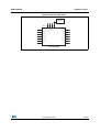
SPBT2932DM
Bluetooth® v4.0 smart ready module
Datasheet - preliminary data
Application
• Serial cable replacement
• M2M industrial control
• Service diagnostic
• Data acquisition equipment
• Machine control
• Sensor monitoring
• Security system
11.6 mm x 13.5 mm
Description
Features
• Bluetooth radio
– Fully embedded Bluetooth v4.0 with
profiles
– Class 1 radio
– 128-bit encryption security
– Integrated antenna
– Dual mode Bluetooth classic and low
energy supported
• ST Micro Cortex-M4 microprocessor up to 84
MHz (256 kb Flash, 48 kb RAM)
• Serial interface
– UART
The SPBT2932DM micro-sized Bluetooth smart
ready module with integrated antenna boasts the
smallest form factor available for a complete RF
platform.
The SPBT2932DM is a surface mount PCB
module that provides fully embedded, ready-touse Bluetooth wireless technology.
The SPBT2932DM supports both Bluetooth
classic and low energy (LE), version v4.0.
Our standard AT command set and Bluetooth
stack are pre-Flashed into the integrated Flash
memory, supporting Bluetooth 3.0 profiles and
Bluetooth 4.0 services. Commands will be listed
in the FW user manual UM1801.
• General I/O
– 8 general purpose I/O
– 1 LPO input
• User interface
– AT command set (abSerial)
– Firmware upgrade over UART
• CE, FCC and BQE qualification (pending)
• Single voltage supply: 2.5 V (typ)
• Micro-sized form factor: 11.6 x 13.5 x 2.9 mm
• RoHS compliance
September 2014
DocID026716 Rev 2
This is preliminary information on a new product now in development or undergoing evaluation. Details are subject to
change without notice.
1/25
www.st.com
Contents
SPBT2932DM
Contents
1
2
Software architecture . . . . . . . . . . . . . . . . . . . . . . . . . . . . . . . . . . . . . . . . 4
1.1
Lower layer stack . . . . . . . . . . . . . . . . . . . . . . . . . . . . . . . . . . . . . . . . . . . . 4
1.2
Upper layer stack: Data FW . . . . . . . . . . . . . . . . . . . . . . . . . . . . . . . . . . . . 4
1.3
AT Command Set . . . . . . . . . . . . . . . . . . . . . . . . . . . . . . . . . . . . . . . . . . . . 4
1.4
Bluetooth firmware implementation . . . . . . . . . . . . . . . . . . . . . . . . . . . . . . 5
Hardware specifications . . . . . . . . . . . . . . . . . . . . . . . . . . . . . . . . . . . . . . 6
2.1
Recommended operating conditions . . . . . . . . . . . . . . . . . . . . . . . . . . . . . 6
2.2
Absolute maximum ratings . . . . . . . . . . . . . . . . . . . . . . . . . . . . . . . . . . . . . 6
2.3
CPU current consumption . . . . . . . . . . . . . . . . . . . . . . . . . . . . . . . . . . . . . 6
2.4
I/O operating characteristics . . . . . . . . . . . . . . . . . . . . . . . . . . . . . . . . . . . . 7
2.5
Selected RF characteristics . . . . . . . . . . . . . . . . . . . . . . . . . . . . . . . . . . . . 7
2.6
Pin assignment . . . . . . . . . . . . . . . . . . . . . . . . . . . . . . . . . . . . . . . . . . . . . . 8
3
Mechanical dimensions . . . . . . . . . . . . . . . . . . . . . . . . . . . . . . . . . . . . . 11
4
Hardware block diagram . . . . . . . . . . . . . . . . . . . . . . . . . . . . . . . . . . . . . 13
5
Hardware design . . . . . . . . . . . . . . . . . . . . . . . . . . . . . . . . . . . . . . . . . . . 14
5.1
Module reflow installation . . . . . . . . . . . . . . . . . . . . . . . . . . . . . . . . . . . . . 14
5.2
GPIO interface . . . . . . . . . . . . . . . . . . . . . . . . . . . . . . . . . . . . . . . . . . . . . 15
5.3
GPIO configuration . . . . . . . . . . . . . . . . . . . . . . . . . . . . . . . . . . . . . . . . . . 15
5.4
UART interface . . . . . . . . . . . . . . . . . . . . . . . . . . . . . . . . . . . . . . . . . . . . . 15
5.5
PCB layout guideline . . . . . . . . . . . . . . . . . . . . . . . . . . . . . . . . . . . . . . . . 17
5.6
Reset circuit . . . . . . . . . . . . . . . . . . . . . . . . . . . . . . . . . . . . . . . . . . . . . . . 17
5.7
2/25
5.6.1
External reset circuit . . . . . . . . . . . . . . . . . . . . . . . . . . . . . . . . . . . . . . . 17
5.6.2
Internal reset circuit . . . . . . . . . . . . . . . . . . . . . . . . . . . . . . . . . . . . . . . . 18
External LPO input circuit . . . . . . . . . . . . . . . . . . . . . . . . . . . . . . . . . . . . . 18
DocID026716 Rev 2
SPBT2932DM
6
Contents
Regulatory compliance . . . . . . . . . . . . . . . . . . . . . . . . . . . . . . . . . . . . . . 20
6.1
FCC and IC certification . . . . . . . . . . . . . . . . . . . . . . . . . . . . . . . . . . . . . . 20
6.2
Bluetooth certification . . . . . . . . . . . . . . . . . . . . . . . . . . . . . . . . . . . . . . . . 20
6.3
CE certification . . . . . . . . . . . . . . . . . . . . . . . . . . . . . . . . . . . . . . . . . . . . . 21
7
Traceability . . . . . . . . . . . . . . . . . . . . . . . . . . . . . . . . . . . . . . . . . . . . . . . . 22
8
Ordering information . . . . . . . . . . . . . . . . . . . . . . . . . . . . . . . . . . . . . . . 23
9
Revision history . . . . . . . . . . . . . . . . . . . . . . . . . . . . . . . . . . . . . . . . . . . 24
DocID026716 Rev 2
3/25
25
Software architecture
SPBT2932DM
1
Software architecture
1.1
Lower layer stack
1.2
1.3
•
Bluetooth v4.0 classic and low energy
•
Device power modes: active, sleep and deep sleep
•
Wake on Bluetooth feature for optimized power consumption of host CPU
•
Authentication and encryption
•
Encryption key length from 8-bits to 128-bits
•
Persistent Flash memory for BD address and user parameter storage
•
All ACL (asynchronous connection-less) packet types
Upper layer stack: Data FW
•
SPP and iAP Classic profiles, battery and private low energy services
•
Protocols: classic (RFCOMM, SDP, L2CAP). Low energy (ATT/GATT)
AT Command Set
The complete command list including the Bluetooth classic and low energy commands is
included in user manual UM1801.
4/25
DocID026716 Rev 2
SPBT2932DM
1.4
Software architecture
Bluetooth firmware implementation
Figure 1. FW architecture
DocID026716 Rev 2
5/25
25
Hardware specifications
2
SPBT2932DM
Hardware specifications
General conditions (VIN= 2.5 V and 25 °C)
2.1
Recommended operating conditions
Table 1. Recommended operating conditions
Rating
Min.
Operating temperature range(1)
-20
Supply voltage VIN
2.0
Signal pin voltage
Typ.
Max.
Unit
60
°C
3.6
V
2.5
2.1
RF frequency
2402
V
2483.5
MHz
Max.
Unit
105
°C
1. T value will be published at the end of module qualification test.
2.2
Absolute maximum ratings
Table 2. Absolute maximum ratings
Rating
Min.
Typ.
Storage temperature range
-55
Supply voltage VIN
-0.3
2.5
5.0
V
I/O pin voltage (VIO five-volt tolerant pin)
-0.3
2.1
5.5
V
-5
dBm
RF input power
2.3
CPU current consumption
•
Standard CPU mode 8 MHz
•
UART supports up to 115 Kbps
•
Data throughput up to 200 Kb
•
FW version 1.5
•
Shallow sleep enabled
Table 3. Current consumption
Modes (typical power consumption)
6/25
Avg
Unit
ACL data 115 K baud UART at max. throughput (master)
16.5
mA
ACL data 115 K baud UART at max. throughput (slave)
18.5
mA
Connection, no data traffic, master
5.2
mA
Connection, no data traffic, slave
7.4
mA
DocID026716 Rev 2
SPBT2932DM
Hardware specifications
Table 3. Current consumption (continued)
Modes (typical power consumption)
Avg
Unit
Connection 375 ms sniff (external LPO required)
590
µA
Standby, without deep sleep
4.9
mA
Standby, with deep sleep, no external LPO
1.2
mA
Standby, with deep sleep, with external LPO
140
µA
Page/inquiry scan, with deep sleep, no external LPO
2.6
mA
Page/inquiry scan, with deep sleep, with external LPO
720
µA
BLE advertising, 1.28sec non-connectable, with external LPO
195
µA
BLE advertising, 1.28sec discoverable, with external LPO
215
µA
11
µA
Bluetooth power down / CPU standby
2.4
I/O operating characteristics
Table 4. I/O operating characteristics
2.5
Symbol
Parameter
Min.
Max.
Unit
Conditions
Vil
Low-level input voltage
-
0.6
V
VIN, 2.1 V
VIH
High-level input voltage
1.4
-
V
VIN, 2.1 V
VOL
Low-level output
voltage
-
0.4
V
VIN, 2.1 V
VOH
High-level output
voltage
1.8
-
V
VIN, 2.1 V
IOL
Low-level output
current
-
4.0
mA
VOL = 0.4 V
IOH
High-level output
current
-
4.0
mA
VOH = 1.8 V
RPU
Pull-up resistor
80
120
kΩ
Resistor turned on
RPD
Pull-down resistor
80
120
kΩ
Resistor turned on
Selected RF characteristics
Table 5. Selected RF characteristics
Parameters
Conditions
Typical(1)
Antenna load
Unit
50 ohm
Radio receiver
Sensitivity level
BER <.001 with DH5
-92
dBm
Maximum usable level
BER <.001 with DH1
0
dBm
DocID026716 Rev 2
7/25
25
Hardware specifications
SPBT2932DM
Table 5. Selected RF characteristics (continued)
Parameters
Conditions
Typical(1)
Input VSWR
Unit
2.5:1
Radio transmitter
Maximum output power
50 Ω load
+ 12
dBm
Initial carrier frequency
tolerance
0
kHz
20 dBm bandwidth for
modulated carrier
935
kHz
1. RF characteristics can be influenced by physical characteristics of final application.
2.6
Pin assignment
Figure 2. Pin connection diagram
8/25
DocID026716 Rev 2
SPBT2932DM
Hardware specifications
Table 6. Pin assignment
Name
Type
Pin #
ALT
function
Description
5 V tolerant
Initial state
UART interface
RXD
I
13
Receive
data
Y
TXD
O
14
Transmit
data
Y
RTS
O
12
Clear to
send (active
low)
I2C data
Y
CTS
I
11
Request to
send (active
low)
I2C clock
Y
Boot loader
Boot 0
I
9
Boot 0
Power and ground
Vin
8
Vin
GND
7
GND
LDout
18
LDO output
2.1 V
Reset
RESETN
I
10
Reset input
(active low
for 5 ms)
(1.8 V +
0.3 V) max.
LPO
LPCLK
I
15
LPO input
GPIO – general purpose input/output
GPIO [1]
I/O
1
General
purpose
input/output
GPIO [2]
I/O
2
General
purpose
input/output
GPIO [3]
I/O
3
GPIO [4]
I/O
GPIO [5]
I/O
Y
Input pull
down
I2S_SD
Y
Floating
General
purpose
input/output
I2S_CLCK
Y
Input pull
down
4
General
purpose
input/output
I2S_WS
Y
Input pull
down
5
General
purpose
input/output
I2C data
Y
Input pull
down
DocID026716 Rev 2
9/25
25
Hardware specifications
SPBT2932DM
Table 6. Pin assignment (continued)
10/25
Name
Type
Pin #
Description
ALT
function
5 V tolerant
Initial state
GPIO [6]
I/O
6
General
purpose
input/output
I2C clock
Y
Input pull
down
GPIO [7]
I/O
17
General
purpose
input/output
ADC 0
Y
Input pull
down
GPIO [8]
I/O
16
General
purpose
input/output
ADC 1
Y
Input pull
down
DocID026716 Rev 2
SPBT2932DM
3
Mechanical dimensions
Mechanical dimensions
In order to meet environmental requirements, ST offers these devices in different grades of
ECOPACK® packages, depending on their level of environmental compliance. ECOPACK®
specifications, grade definitions and product status are available at: www.st.com.
ECOPACK® is an ST trademark.
Figure 3. Mechanical dimensions
DocID026716 Rev 2
11/25
25
Mechanical dimensions
SPBT2932DM
Figure 4. Recommended land pattern
12/25
DocID026716 Rev 2
SPBT2932DM
4
Hardware block diagram
Hardware block diagram
Figure 5. SPBT2932DM module block diagram
DocID026716 Rev 2
13/25
25
Hardware design
5
SPBT2932DM
Hardware design
The SPBT2932DM module supports UART and GPIO hardware interfaces.
Please note that:
5.1
•
All unused pins should be left floating; do not ground.
•
All GND pins must be well grounded.
•
The area around the module should be free of any ground planes, power planes, trace
routings, or metal for 6 mm from the antenna in all directions.
•
Traces should not be routed underneath the module.
Module reflow installation
The SPB2932DM is a surface mount Bluetooth module supplied on an 18-pin, 6-layer PCB.
The final assembly recommended reflow profiles are indicated below.
The soldering phase must be executed with care. In order to avoid the undesired melting,
particular attention must be taken during the setup of the peak temperature.
The following provides some suggestions for the temperature profile based on IPC/JEDEC
J-STD-020C, July 2004 recommendations.
Table 7. Soldering
Profile feature
Average ramp-up rate (TSMAX to Tp)
Preheat
Temperature min (TS min)
Temperature max (TS max)
Time (tS min to tS max) (tS)
PB-free assembly
3 °C/sec max
150 °C
200 °C
60-100 sec
Time maintained above:
Temperature TL
Time tL
217 °C
60-70 sec
Peak temperature (Tp)
240 + 0 °C
Time within 5 °C of actual peak temperature (tP)
10-20 sec
Ramp-down rate
6 °C/sec
Time from 25 °C to peak temperature
14/25
DocID026716 Rev 2
8 minutes max
SPBT2932DM
Hardware design
Figure 6. Soldering profile
5.2
GPIO interface
All GPIOs are capable of sinking and sourcing 6 mA of I/O current. GPIO [1] to GPIO [8] are
internally pulled down with 100 kΩ (nominal) resistors, except GPIO [2], which is floating.
5.3
GPIO configuration
Module GPIO configuration depends on the FW embedded.
GPIO can be reconfigured using the following commands:
•
At+ab gpioconfig [GPIO pin] [I/O]
•
At+ab gpioRead [GPIO pin]
•
At+ab gpioWrite [GPIO pin] [1/0]
For additional details, refer to user manual UM1801.
5.4
UART interface
The UART is compatible with the 16550 industry standard. Four signals are provided with
the UART interface. The TXD and RXD pins are used for data while the CTS and RTS pins
are used for flow control.
DocID026716 Rev 2
15/25
25
Hardware design
SPBT2932DM
Figure 7. Connection to host device
Figure 8. Typical RS232 circuit
16/25
DocID026716 Rev 2
SPBT2932DM
5.5
Hardware design
PCB layout guideline
Figure 9. PCB layout guideline
5.6
Reset circuit
Two types of system reset circuits are detailed below. The maximum voltage that can be
supplied to the RESET pin is 2.5 V. As shown in Figure 10 and Figure 11, the RESET is
active low. In the absence of a reset circuit, the pin is internally pulled up and therefore
inactive.
5.6.1
External reset circuit
Figure 10. External reset circuit
Note:
RPU ranges from 30 kW to 50 kW internally.
DocID026716 Rev 2
17/25
25
Hardware design
5.6.2
SPBT2932DM
Internal reset circuit
Figure 11. Internal reset circuit
Note:
RPU ranges from 30 kW to 50 kW internally.
RRST should be from 1 kW to 10 kW.
5.7
External LPO input circuit
An optional low power oscillator input may be added to allow deep sleep and sniff modes.
•
LPO parameters:
•
–
Frequency: 32.768 kHz
–
Tolerance: +/- 150 ppm typical, +/- 250 maximum
–
Absolute maximum supplied voltage at LPO pin: +1.8 V
–
VIL min/max = 0 V/+0.5 V
–
VIH min/max = +1.47 V/+1.8 V
–
Input capacitance: 2.5 pF maximum
Configurations:
–
Use two configuration variables: UseExtLPO and AllowSniff.
Table 8. System configuration variables
Variable
18/25
Name
Default
Description
Var..
UseExtLPO
auto
True when a 32.768 kHz low power oscillator is present,
and false if not present.
Var..
AllowSniff
false
Enables sniff mode. Must be false when no 32.768 kHz
LPO is present.
DocID026716 Rev 2
SPBT2932DM
Hardware design
Figure 12. External LPO circuit
G PIO02
3
4
16
17
15
LPO
2
G PIO08
G PIO01
G PIO07
1
LDOUT
B T1
18
LPO
T XD
14
R XD
13
G PIO03
R TS
12
G PIO04
C TS
11
5
G PIO05
R ES ET
10
6
G PIO06
BOOT
9
7
G ND
V IN
8
S PB T2932DM
DocID026716 Rev 2
19/25
25
Regulatory compliance
SPBT2932DM
6
Regulatory compliance
6.1
FCC and IC certification
This module has been tested and found to comply with the FCC part 15 and IC RSS-210
rules. These limits are designed to provide reasonable protection against harmful
interference in approved installations. This equipment generates, uses, and can radiate
radio frequency energy and, if not installed and used in accordance with the instructions,
may cause harmful interference to radio communications.
However, there is no guarantee that interference may not occur in a particular installation.
This device complies with part 15 of the FCC rules. Operation is subject to the following two
conditions:
1.
this device may not cause harmful interference
2.
this device must accept any interference received, including interference that may
cause undesired operation.
Modifications or changes to this equipment not expressly approved by the part responsible
for compliance may render void the user's authority to operate this equipment.
–
Modular approval, FCC and IC
FCC ID: X3ZBTMOD7
IC: 8828A-MOD7
In accordance with FCC part 15, the SPBT2932DM is listed above as a modular transmitter
device.
–
Label instructions
When integrating the SPBT2932DM into the final product, it must be ensured that the FCC
labeling requirements, as specified below, are satisfied. Based on the public notice from
FCC, the product into which the ST transmitter module is installed must display a label
referring to the enclosed module. The label should use wording such as the following:
Contains transmitter module
FCC ID: X3ZBTMOD7
IC: 8828A-MOD7
Any similar wording that expresses the same meaning may be used.
6.2
Bluetooth certification
The module with embedded stack and profile has been qualified according to SIG
qualification rules:
20/25
•
Bluetooth SIG Qualified Design, QD ID: 58674
•
Product type: End Product
•
TGP version: Core 4.0
•
Core spec version: 4.0
•
Product descriptions: Bluetooth module, spec v4.0
DocID026716 Rev 2
SPBT2932DM
6.3
Regulatory compliance
CE certification
Module has been certified according to following certification rules:
•
CE Expert Opinion: TBD
•
Measurements have been performed in accordance with (report available on request):
–
EN 300 328 V 1.8.1 (2012 06) (a)
–
EN 301 489-17 V 2.2.1 (2012 09) (b)
–
EN 301 489 -1 V 1.9.2 (2011 09) (c)
–
EN60950-1:2006 +A11:2009+A1:2010 (d)
CE certified:
a. EN 300 328 V 1.8.1 (2012 06): “Electromagnetic compatibility and radio spectrum matters (ERM); Wideband
transmission systems; data transmission equipment operating in the 2.4 GHz ISM band and using wideband
modulation techniques; harmonized EN covering essential requirements under article 3.2 of the R&TTE
directive”.
b. EN 301 489-17 V 2.2.1 (2012 09): “Electromagnetic compatibility and radio spectrum matters (ERM);
Electromagnetic compatibility (EMC) standard for radio equipment and services; part 17: specific condition for
2.4 GHz wideband transmission systems and 5 GHz high performance RLAN equipment”.
c. EN301 489-1 V 1.9.2 (2011 09): “Electromagnetic compatibility and radio spectrum Matters (ERM);
Electromagnetic compatibility (EMC) standard for radio equipment and services; part 1: Common technical
requirements”.
d. EN60950-1:2006 +A11:2009+A1:2010: “Information technology equipment - safety”.
DocID026716 Rev 2
21/25
25
Traceability
7
SPBT2932DM
Traceability
Each module is uniquely identified by a serial number stored in a 2D data matrix lasermarked on the bottom side of the module.
The serial number has the following format:
WW YY D FF NNN
Where:
–
WW = week
–
YY = year
–
D = product ID family
–
FF = production panel coordinate identification
–
NNN = progressive serial number
Each module bulk is identified by a bulk ID.
Bulk ID and module 2D data matrix are linked by a reciprocal traceability link.
The module 2D data matrix traces the lot number of any raw material used.
22/25
DocID026716 Rev 2
SPBT2932DM
8
Ordering information
Ordering information
Table 9. Ordering information
Order code
Description
Packing
MOQ
SPBT2932DM
Bluetooth V4.0 data module
JEDEC tray
2448 pcs
DocID026716 Rev 2
23/25
25
Revision history
9
SPBT2932DM
Revision history
Table 10. Document revision history
24/25
Date
Revision
Changes
05-Sep-2014
1
Initial release.
23-Sep-2014
2
Table 1 has been modified.
Document status promoted from product preview to
preliminary data.
DocID026716 Rev 2
SPBT2932DM
IMPORTANT NOTICE – PLEASE READ CAREFULLY
STMicroelectronics NV and its subsidiaries (“ST”) reserve the right to make changes, corrections, enhancements, modifications, and
improvements to ST products and/or to this document at any time without notice. Purchasers should obtain the latest relevant information on
ST products before placing orders. ST products are sold pursuant to ST’s terms and conditions of sale in place at the time of order
acknowledgement.
Purchasers are solely responsible for the choice, selection, and use of ST products and ST assumes no liability for application assistance or
the design of Purchasers’ products.
No license, express or implied, to any intellectual property right is granted by ST herein.
Resale of ST products with provisions different from the information set forth herein shall void any warranty granted by ST for such product.
ST and the ST logo are trademarks of ST. All other product or service names are the property of their respective owners.
Information in this document supersedes and replaces information previously supplied in any prior versions of this document.
© 2014 STMicroelectronics – All rights reserved
DocID026716 Rev 2
25/25
25