1
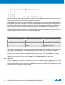
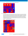
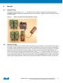
APPLICATION NOTE
AT08973: SAMR21 Basic Connections and Wireless
Design
SAMR21
Introduction
This reference design showcases ATSAMR21G Wireless System-in-Package and
several design techniques for RF PCB construction; controlled impedance, PCB
antenna and interface, microstrip layout, ground-plane segregation, star
grounding, conducted RF test point, and several other features that are good
practice for RF layout.
Features
• Basic Connections for SAMR21
• RF Layout for SAMR21
• Microstrip
• PCB Antenna
• Ground-plane System
• Reference design and analysis
• Schematics and BOM
• Altium design database
• FCC Pre-scan data
Atmel-42391A-SAMR21-Basic-Connections-and-Wireless-Design-ApplicationNote_012015
Ta bl e of Conte nts
1
Overview ..................................................................................................................................3
1.1
1.2
1.3
2
Implementation .........................................................................................................................5
2.1
2.2
3
Stack-up and Material ........................................................................................................................................ 12
Grounding Plan .................................................................................................................................................. 12
3.2.2 NET-TIES .............................................................................................................................................. 14
3.2.3 Copper-pour .......................................................................................................................................... 15
3.2.4 Via-Stitching .......................................................................................................................................... 16
3.2.5 QA Testing............................................................................................................................................. 16
3.2.6 Clean Assembly..................................................................................................................................... 16
Results
4.1
4.2
4.3
4.4
4.5
2
Required Elements Area ...................................................................................................................................... 5
2.1.2 Antenna System ...................................................................................................................................... 5
2.1.3 Adjusting the Ground-plane ..................................................................................................................... 6
2.1.4 RF Test Point........................................................................................................................................... 6
2.1.5 PI Tuning Network ................................................................................................................................... 7
2.1.6 Transmission Line ................................................................................................................................... 8
2.1.7 Balun ....................................................................................................................................................... 8
2.1.8 Local Oscillator ........................................................................................................................................ 8
2.1.9 Power Rails and Bypass Capacitors........................................................................................................ 9
2.1.10 External Power Connections ................................................................................................................... 9
2.1.11 Programming and UART Headers ........................................................................................................... 9
Recommended Accessories Area ...................................................................................................................... 10
2.2.2 User Defined Button .............................................................................................................................. 11
2.2.3 User Defined LEDs ................................................................................................................................ 11
2.2.4 User Defined GPIO................................................................................................................................ 11
2.2.5 Power Header........................................................................................................................................ 11
2.2.6 Current Measurement Shunt ................................................................................................................. 11
2.2.7 4Mb Serial Flash Memory ...................................................................................................................... 11
Printed Circuit Board Design .................................................................................................12
3.1
3.2
4
Description ........................................................................................................................................................... 3
Background .......................................................................................................................................................... 3
Design Partitions .................................................................................................................................................. 4
................................................................................................................................17
Sample Group .................................................................................................................................................... 17
Antenna Tuning .................................................................................................................................................. 17
Receiver Testing ................................................................................................................................................ 19
Intentional Emissions ......................................................................................................................................... 22
Unintentional Emissions ..................................................................................................................................... 23
4.5.1 Sub-GHz Emissions .............................................................................................................................. 23
4.5.2 Band-Edge............................................................................................................................................. 24
4.5.3 High-Frequency Emissions .................................................................................................................... 24
5
Conclusion ..............................................................................................................................27
6
Reference ................................................................................................................................27
7
Revision History .....................................................................................................................28
SAMR21 Basic Connections and Wireless Design [APPLICATION NOTE]
Atmel-42391A-SAMR21-Basic-Connections-and-Wireless-Design-ApplicationNote_012015
1
Overview
1.1
Description
®
This application note illustrates the basic circuitry needed to use the Atmel ATSAMR21G 48 Pin QFN
®
(SAMR21). The SAMR21 is a System-in-Package (SIP) device that includes a 2.4GHz IEEE 802.15.4
®
®
Transceiver and an ARM Cortex M0+ microcontroller. To archive satisfactory performance designers need to
adhere to good RF design practices. This reference design showcases several RF design techniques including:
controlled impedance, PCB antenna interface, microstrip layout, ground-plane segregation, star grounding,
conducted RF test point, and several other features that are good practice for RF layout. This design is
compartmentalized in to two blocks; the Required Elements and Recommended Accessories.
Figure 1-1.
1.2
Ramen PCBAs
Background
When Implementing an RF design with new chip-set, engineers need to know the basic required elements and
how to connect them. RF designs are risky because the PCB layout is critical and many engineers are not
familiar with RF design practice. This design identifies the required elements and connections needed for
success with Atmel ATSAMR21. This design uses a PCB antenna and 50Ω unbalanced transmission line with a
coax RF test point. This combination has proven to be straight forward to implement, optimal for regulatory
testing, and mass-production with Automated Test Equipment (ATE). The minimal design is implemented in a
separate region of the PCB and can be cut-and-pasted into a new system as a whole. This design also identifies
several recommended accessories such as serial flash memory and 32kHz crystal oscillator that have proven
useful in practical systems.
On PCBs many RF circuits are atypical and trigger CAD tool Design Rule Check (DRC) errors. For example PCB
antennas are effectively DC shorts. Another example is ground-planes. The ATSAMR21 uses several
independent ground domains. Star Ground techniques are desirable to reduce common impedance coupling of
electro Magnetic Interference (EMI) and baseband crosstalk. These objectives conflict with normal CAD practice.
Another exception is management of copper pouring on top and bottom layers. There is some debate of the
usefulness of copper pour with microstrip however, if this technique is desired some basic guidelines need to be
followed. Effective techniques to manage these exceptions are outlined in this paper.
SAMR21 Basic Connections and Wireless Design [APPLICATION NOTE]
Atmel-42391A-SAMR21-Basic-Connections-and-Wireless-Design-ApplicationNote_012015
3
1.3
Design Partitions
This design has two sections; the required elements and the recommended accessories. These have been
partitioned into two schematic sheets and separate areas in the PCB layout. Refer to the schematics in the
RAMEN_DOCS.zip design folder. The RF section includes a 50Ω unbalanced microstrip transmission line and a
PCB antenna.
Figure 1-2.
Ramen Layout
The PCB uses a four layer stack-up to implement controlled impedance and a low impedance ground return for
the antenna system. The ground-plane of the required section is the correct size and orientation to counterpoise
the PCB antenna. The required section also includes programming and UART headers. These two interfaces are
necessary for debug and mass-production with ATE.
The accessories section shows several accessories that have proven useful in practical designs. A 4Mb serial
flash provides extra storage space for over the air (OTA) programming and general usage. Many wireless
standards such as ZigBee Light Link now require OTA programming. Additional features include a RESET*
button, one general purpose push button, and three LEDs and GPIO headers. A 32kHz crystal is also shown in
the accessories section of the schematics because it is not required and can be omitted. If this crystal is used
however, it needs to be placed close to the CPU so it is physically located in the required area of the layout. One
final feature is the low-side DC shunt. Atmel ATSAMR21 is one of the lowest power solutions on the market the
shunt is provided to make accurate line-power measurements with grounded test equipment.
4
SAMR21 Basic Connections and Wireless Design [APPLICATION NOTE]
Atmel-42391A-SAMR21-Basic-Connections-and-Wireless-Design-ApplicationNote_012015
2
Implementation
2.1
Required Elements Area
Figure 2-1.
2.1.2
Required Elements Area
Antenna System
The heart of any radio design is the antenna. This design uses an Inverted F Antenna (IFA). The IFA is a classic
PCB antenna that is a good performer with minimal cost. The IFA antenna is a quarter-wave monopole antenna
and requires a ground-plane to function. This antenna works because it sets up an electric field in the gap
between the resonant stub and the ground-plane.
The nominal size of the ground-plane is one quarter by one half wavelengths. The ground-plane collects RF
energy in receive mode; the amount of energy collected is directly proportional to the area, or effective aperture.
In transmission mode, an African kalimba is a good allegory for the IFA System. The tines of the kalimba are
quarter wave resonators and the body is similar to the ground-plane. The body has sustained standing waves
resonating in multiple modes, size, and shape influences the efficiency and tone of the system. The same is true
for the ground-plane of our IFA system; size and shape influence efficiency and tone.
Figure 2-2.
Kalimba and Ramen
SAMR21 Basic Connections and Wireless Design [APPLICATION NOTE]
Atmel-42391A-SAMR21-Basic-Connections-and-Wireless-Design-ApplicationNote_012015
5
This transmitter operates in the 2.4GHz ISM band. In free space the wave length of 2.4GHz is approximately 4.8
inches (123mm). Hence a quarter-wave is 1.2 inches. When the IFA is placed on a PCB the relative permittivity of
the material reduces the wavelength by slowing the propagation of the TEM wave. In this design we are
[5]
assuming the PCB material is FR-4 and has a velocity factor of about 0.7 . This results in a quarter-wavelength
of 880mils (22mm). The nominal dimensions of the resonator and the ground-plane are defined using this length.
2.1.3
Adjusting the Ground-plane
Many designers want smaller dimensions everywhere. The Required Elements Area is the minimum
recommended layout size. Reducing the ground-plane on RF designs has many risks; reduced receiver
efficiency from loss of area, de-tuning of antenna match, and increased influence of random parasitic reactance.
These problems can reduce radio-link range and reduce yield in mass-production. Chip antennas are often
suggested as a compact alternative to PCB antennas but critical evaluation of datasheets reveals the
ground-planes used to characterize these components are often quite large. To reduce size designers can add
components to the back side of the required elements area as long the gap between the antenna and the
ground-plane is kept clear.
For those that want to expand the ground-plane, the lateral dimension (X) of the RF ground plane should be
preserved; additional ground-planes to the sides should be isolated with slots. This isolates the resonant
structure and allows designers to expand their base-band circuitry with minimal interferences.
Figure 2-3.
2.1.4
Expanded Ground-plane with Slot Partition
RF Test Point
RFTP1 is an RF test point. This is used to test the RF signal using a coaxial probe. This is very useful for
engineering characterization, regulatory testing and mass production testing with ATE. The test point is a
“Switch-Connector” type when the probe is inserted the RF signal is routed to the probe. When the probe is
removed the signal passes through the component to the PCB antenna. The test point has been oriented to
connect the ATSAMR21 to the test instrument. In this way spectrum analyzers and RF test instruments can be
used to make conducted measurements of RF output.
6
SAMR21 Basic Connections and Wireless Design [APPLICATION NOTE]
Atmel-42391A-SAMR21-Basic-Connections-and-Wireless-Design-ApplicationNote_012015
Figure 2-4.
2.1.5
RF Automated Test Equipment Using RFTP
PI Tuning Network
At the base of the antenna we have placed a PI network for tuning the match. The final values will be selected
after the PCBA has been assembled and the radio can be tuned inside an enclosure. For initial engineering
prototyping the series position (C6) is loaded with a DC blocking capacitor of 20pF and the shunt positions (C5
and C7) are left open. Additionally the RF test point can be rotated 180 degrees which connects the antenna and
PI network to the test immurements. In this way a Vector Network Analyzer (VNA) can be used to tune the
antenna and adjust the matching network.
Figure 2-5.
Probing the Antenna with RFTP1
SAMR21 Basic Connections and Wireless Design [APPLICATION NOTE]
Atmel-42391A-SAMR21-Basic-Connections-and-Wireless-Design-ApplicationNote_012015
7
2.1.6
Transmission Line
To efficiently conduct RF power between the ATSAMR21 and the Antenna System this design uses a 50Ω
unbalanced (single-ended) microstrip transmission line. Microstrip transmission lines are covered in detail in RF
[2]
Layout with Microstrip . In this design we use a 20mil (0,5mm) transmission line and a 10mil (0,25mm) dielectric
to achieve the 50Ω impedance. 20mil transmission lines neatly abut to 0402 components. Layer-1 is
pushed-back by 40mils from the microstrip to reduce parasitic coupling. In Figure 2-6 the RF Ground-plane is not
visible because the CAD tool uses a negative image.
Figure 2-6.
Transmission Lines inside Green Boarders
To connect the balun to the ATSAMR21 balanced 100Ω transmission lines are used. This technique is also
[2]
detailed in RF Layout with Microstrip . The balanced transmission lines are designed with a 20mil
center-to-center spacing that mates directly to the pins of the SAMR21.
2.1.7
Balun
The balun is an essential component. It converts the balanced output of the ATSAMR21 to the unbalanced 50Ω
transmission line. 50Ω transmission lines are easy to use and are the interface of choice for RF test equipment
and RF components such as switches, filters and PA/LNA range extenders. Internally the ATSAMR21 uses a
balanced 100Ω signals. Balanced signals have several advantages for IC designers; they increase the receiver
signal-to-noise ratio, suppress even harmonics of the transmitter and can be controlled with high-speed current
steering circuitry. Unfortunately balanced signals are difficult for PCB designers to route and use. The balun used
in this example provides two additional features; DC blocking and Low-Pass Filtering. The DC blocking is needed
because the balanced signals have a common mode voltage of 900mV, shorting this to grounded test equipment
will kill the RF signal. The Low-Pass filter suppresses harmonic emissions, EMI, and improves ESD resilience.
This example uses a balun which has been customized to match the Atmel ATSAMR21. Matching generic or
discrete baluns to Atmel ATSAMR21 is beyond the scope of this document and is not recommended.
2.1.8
Local Oscillator
This design uses a 16MHz crystal oscillator for the RF synthesizer. The ATSAMR21 uses special circuitry to
drive the PLL in coordination with sleep management. For low-power designs a dedicated crystal is
8
SAMR21 Basic Connections and Wireless Design [APPLICATION NOTE]
Atmel-42391A-SAMR21-Basic-Connections-and-Wireless-Design-ApplicationNote_012015
[3]
recommended. Atmel application note AVR2067 Crystal Characterization for AVR RF covers the use of
crystals in detail. In general the crystal signal quality directly influences the RF signal quality. Jitter, phase-noise
and drift are all mixed with the carrier and impact modulation quality, radio-link range and spurious emissions.
Good quality crystals with low drift are recommended for high-performance designs. Designers may want to add
a resistor in series with the crystal to test safety margin but this was omitted in this minimal implementation.
2.1.9
Power Rails and Bypass Capacitors
The ATSAMR21 has several internal power domains that need to be factored into the design. In this PCB design
we used two domains D3V3 and A3V3 for digital and analog power rails. Both of these rails have ferrite beads to
suppress VHF noise, 10µF bulk bypass caps for local charge reserve and 20pF caps to shunt RF to ground.
Clean power is required to keep noise out of mixers and receiver stages. To this end, ATSAMR21 includes two
on-board regulators (LDOs): AVDD and DVDD. These LDOs need external compensation caps. The
recommended values of 0.1µF are used. Additionally 20pF caps are added to shunt RF to ground. AVDD and
DVDD are throttled as the CPU changes sleep states. These rails should not be used as external references or
supplies. Additionally use of large value compensation caps on AVDD and DVDD is not recommended and may
delay the PLL ramp-up time and destabilize the LDO control loops.
2.1.10 External Power Connections
System designers should connect their power source to the RAW_3V3 bus. AC lines should be filtered to reduce
conducted emissions from the transmitter. The D3V3 and A3V3 busses can be used sparingly for support
circuitry like analog signal conditioning and glue logic but the ferrite beads L1 and L2 are limited to 500mA
current.
2.1.11 Programming and UART Headers
Atmel strongly recommends preserving programming and UART interfaces for the life of the product. UARTs
enable Automated Test Equipment (ATE) for efficient mass-production. Debugging interfaces are invaluable in
development. Programming interfaces will significantly reduce the impact of firmware updates and product
recalls. Programming and UART headers have been included in the Required Elements Area. The Debugging
header is the industry standard pin assignment for Cortex. This board can be programmed using the Atmel-ICE
Basic programmer dongle. The UART is simple 3x1 x 100mil header with a CMOS interface. This can be
connected to generic USB/UART converter cables. The pin assignments for the Programming and UART
headers are shown in Table 2-1 and Table 2-2.
Table 2-1.
Programming Header Pin Assignment
PIN
SIGNAL
J1.1
D3V3
J1.2
PA31_SWDIO
J1.3
DGND
J1.4
PA30_SWCLK
J1.5
DGND
J1.6
N/C
J1.7
N/C
J1.8
N/C
J1.9
DGND
J1.10
RESET*
SAMR21 Basic Connections and Wireless Design [APPLICATION NOTE]
Atmel-42391A-SAMR21-Basic-Connections-and-Wireless-Design-ApplicationNote_012015
9
Table 2-2.
2.2
UART Header Pin Assignment
PIN
SIGNAL
J2.1
DGND
J2.2
PA25-UART_RX
J2.3
PA24-UART_TX
Recommended Accessories Area
Several features were added to the recommended accessories area. The recommended accessories selected
have proven useful in many development projects but they are optional and can be taken as needed in derivative
designs. The accessories include:
•
On-Off Switch
•
Battery Pack
•
Manual Reset
•
User defined button
•
User defined LEDs
•
GPIO Headers
•
Power Header
•
Current measurement shunt
•
4Mb Serial Flash
The utility of most of these accessories is obvious, but a few need expanded comments.
Figure 2-7.
10
Recommended Accessories Area
SAMR21 Basic Connections and Wireless Design [APPLICATION NOTE]
Atmel-42391A-SAMR21-Basic-Connections-and-Wireless-Design-ApplicationNote_012015
2.2.2
User Defined Button
This button is provided for general use or binding stimulus. The button is active low and connected to PA06.
2.2.3
User Defined LEDs
These three green lamps are provided for general use. The connections are shown in Table 2-3.
Table 2-3.
2.2.4
User Defined Lamps
LED
SIGNAL
D1
PA28
D2
PB02
D3
PA07
User Defined GPIO
The four GPIO headers are detailed in Table 2-4. By convention, pin 1 is ground.
Table 2-4.
2.2.5
GPIO Header Pin Assignments
PIN
SIGNAL
PIN
SIGNAL
PIN
SIGNAL
PIN
SIGNAL
J5.1
DGND
J6.1
DGND
J7.1
DGND
J8.1
DGND
J5.2
PA16-SPI_MISO
J6.2
PA06
J7.2
PA04
J8.2
PB02
J5.3
PA17-SPI_SS*
J6.3
PA07
J7.3
PA05
J8.3
PB03
J5.4
PA18-SPI_MOSI
J6.4
PA08-I2C_SCA
J7.4
PA27
J8.4
PB22
J5.5
PA19-SPI_SCLK
J6.5
PA09-I2C_SCL
J7.5
PA28
J8.5
PB23
Power Header
Header J3 is provided as an auxiliary power input. If users remove the batteries, they may power the board using
this jack. Alternatively they can draw battery power from this header to power off-board circuitry.
2.2.6
Current Measurement Shunt
Header J4 is provided to probe the current shunt. The shunt allows developers to measure fast transient currents
with an oscilloscope. This is a low-side shunt that can be connected directly to earth grounded lab equipment.
For example line-current and conducted RF signals can be measured simultaneously while using grounded ICE
programmer. Pin 1 should be grounded. Pin 2 is used for measurement. A positive current through the SAMR21
will produce a negative voltage across this shunt. For critical measurements of low power, nonessential devices
will have to be de-populated from the PCBA.
2.2.7
4Mb Serial Flash Memory
A socket is provided for Serial Memory. This can be used to Over the Air (OTA) upgrades, storing credentials, or
general purpose memory. The SPI bus connected to this memory is also routed to the J5 header.
SAMR21 Basic Connections and Wireless Design [APPLICATION NOTE]
Atmel-42391A-SAMR21-Basic-Connections-and-Wireless-Design-ApplicationNote_012015
11
3
Printed Circuit Board Design
3.1
Stack-up and Material
The board was designed as an example for RF layout for the ATSAMR21G. This board is a four-layer PCB that
uses microstrip and a PCB antenna. Four-layers are recommended for low-risk development. More than four
layers can be used if the additional layers are inserted beneath the RF Ground-plane on Layer-2. Two-Layer
PCBs are possible using Coplanar Waveguide techniques but they have inferior grounding which typically results
in abundant spurious emissions. The layers used in this design are shown below:
•
Layer-1 RF signals and copper-pour
•
Layer-2 RF ground-plane exclusively
•
Layer-3 Digital ground-plane and power traces
•
Layer-4 General purpose signals and copper-pour
To implement microstrip transmission lines on Layer-1 the dielectric thickness and trace width are chosen using
a 2:1 rule of thumb. The traces are 20mils wide and the dielectric is 10mils thick. A 10mil sheet of good quality
core was used between Layer-1 and Layer-2. This gives a more consistent dielectric thickness than prepreg.
Prepreg is used between Layer-2 and Layer-3 as filler for compliance. The stack-up is shown in Figure 3-1.
Figure 3-1.
3.2
Ramen PCB Stack-up
Grounding Plan
The layer stack-up was assigned to provide a continuous RF ground-plane and keep the multiple ground
domains organized in a straight forward manner. Close review of the ATSAMR21 datasheet Section 5.2.3 2.4
ISM Band Transceiver Connections reveals several different ground domains and how they are internally
connected. The challenge is to manage the ground domains on the PCB rationally.
12
SAMR21 Basic Connections and Wireless Design [APPLICATION NOTE]
Atmel-42391A-SAMR21-Basic-Connections-and-Wireless-Design-ApplicationNote_012015
Figure 3-2.
SAMR21 Internal Connections
There are several opposing design objectives; one design objective is prevention of common impedance
coupling. For example the local oscillator grounds or digital communication bus returns from mixing with the RF
ground currents.
SAMR21 Basic Connections and Wireless Design [APPLICATION NOTE]
Atmel-42391A-SAMR21-Basic-Connections-and-Wireless-Design-ApplicationNote_012015
13
Figure 3-3.
Undesirable Common Impedance Coupling
Star grounding is the usual technique employed to reduce common impedance coupling. Classical Analog layout
implements star grounding by connecting ground domains “at the IC”.
Another objective is to provide a large and stable RF ground-plane as a counterpoise to the PCB antenna and
low impedance return path for RF signals. For superior signal strength these return currents need to freely flow to
the “Paddle” of the SAMR21 and to the ground pins of the Balun. The paddle of the SAMR21 is for RF Ground
return, not thermal conduction. ATSAMR21 is an ultra low-power device that does not need extra cooling.
Because we are using microstrip, Layer-2 is the primary RF ground however this design also uses Copper-pour
on the top and bottom layers. Copper-pour is a popular design technique used to reduce EMI and it also gives a
good solid ground connection to the RF components on the top layer.
We want to do all this without confusing the layout tool and suffering a barrage of DRC Errors.
Table 3-1.
Stack-up Ground Plan
Layer
Name
Ground domains allowed
1
Top
AGND (traces), RFGND (copper pour)
2
RFGND
RFGND (full plane)
3
DGND/3V3
DGND (split plane)
4
Bottom
RFGND (copper pour)
The layout plan was developed to keep the signals rationally organized. In the PCB design three ground domains
were assigned: RFGND, AGND, and DGND. RFGND was used for the primary return path for RF signals.
RFGND was implemented with a full Ground-Plane on Layer-2. AGND is used for the local oscillators and analog
systems on the Transceiver and CPU. AGND was implemented on Layer-1 with traces. DGND is the digital
return path for baseband communication busses and digital logic. DGND was placed on Layer-3 as a mixed
plane with power traces. In this way each ground domain is compartmentalized to a single layer.
3.2.2
NET-TIES
To join the ground domains “at the IC”, all three domains flow to the Paddle under the SAMR21 then NET-TIES
are used on the top layer to join the various ground pins of the SAMR21 to the Paddle. NET-TIEs are metal
shoring links that directly connect the pad to the paddle. More information on NET-TIES is available in AT11309
[6]
Advanced Layout Techniques for Wireless PCBs .
14
SAMR21 Basic Connections and Wireless Design [APPLICATION NOTE]
Atmel-42391A-SAMR21-Basic-Connections-and-Wireless-Design-ApplicationNote_012015
Figure 3-4.
3.2.3
NET-TIES NT29 and NT35 Connect RFGND to DGND “At the IC”
Copper-pour
In this design Copper-pour is used on the top and bottom layers. The Copper-pour was assigned to the RFGND
Domain and is connected to Layer-2 with via stitching. Care should be taken with Copper-pour to avoid floating
islands and narrow peninsulas. Floating Islands act as shields and peninsulas act as radiators. In this design the
Copper-Pour tool of the CAD system was configured to connect all pour areas to RFGND, remove small areas of
dead copper, and keep the pour away from the microstrip transmission line. Microstrip works because of the
controlled dielectric thickness and the idyllic assumption that the primary ground on Layer-2 is an infinite plane.
Pulling back the Copper-pour on Layer-1 by four times the dielectric thickness reduces secondary ground effects
to less than 10% of the 50Ω impedance.
Figure 3-5.
Copper-pour Near U1 and Transmission Lines
SAMR21 Basic Connections and Wireless Design [APPLICATION NOTE]
Atmel-42391A-SAMR21-Basic-Connections-and-Wireless-Design-ApplicationNote_012015
15
3.2.4
Via-stitching
And finally via-stitching joins the RFGND Layers together near the edges of the PCB to reduce unwanted
spurious emissions and edge effects. The via-stitching connects the RF Ground-plane on Layer-2 with
Copper-pour on Layer-1 and Layer-4. The via-stitching does not connect to the DGND plane. The DGND plane
can be used to guide the placement of the automated via-stitching tool in this CAD tool.
3.2.5
QA Testing
To verify the microstrip a test coupon was generated. The test coupon is built along with the PCB so it has
identical properties. The fabrication house can verify the impedance of the test coupon using a Time Domain
Reflectometer (TDR). Because the Test Coupon and Microstrip transmission line are identical, they will have the
same impedance. This final QA step insures the design plan has been successful we will get maximum efficiency
from the RF transmission line and consistent lot-to-lot yield.
3.2.6
Clean Assembly
Cleanliness counts. The ATSAMR21 is an ultra-low-power wireless device. Ionic contamination and debris on
PCBAs can rob precious battery power and de-tune the RF signal path. No-Clean assembly processes will give
the best results. If water soluble flux is used, double washing in de-ionized water and twenty-four hour bake
under heat lamps is recommended.
16
SAMR21 Basic Connections and Wireless Design [APPLICATION NOTE]
Atmel-42391A-SAMR21-Basic-Connections-and-Wireless-Design-ApplicationNote_012015
4
Results
4.1
Sample Group
The sample group is shown in Figure 4-1. The project name is “Ramen”, a popular food and an anagram of
ATSAMR21. Individual PCBAs were identified with sea creature stickers. Testing includes Rx Sensitivity and TX
emissions testing.
Figure 4-1.
4.2
Sample Lot of Ramen Assemblies Ready for Testing
Antenna Tuning
One of the first tasks after receiving the PCBs is trimming and tuning the antenna. The dimensions of the antenna
are roughly correct, but adjustments need to be made to compensate for enclosures and variance in fabrication.
The antenna length is slightly longer than necessary. This makes the resonant frequency slightly flat. The optimal
length can be found by trimming the antenna length in small increments to get the best signal strength. This
demo board was trimmed using a Vector Network Analyzer (VNA). Figure 4-2 shows the return loss. A return loss
of -12 or less indicates better than 90% of the RF energy is dissipated in the antenna. After trimming off 50mils of
length off the tip, the antenna is showing strong resonance in the 2400-2480MHz band. If a VNA is not available,
simple signal RF Signal strength measurements using the Atmel Studio 6 Performance Analyzer can be used.
SAMR21 Basic Connections and Wireless Design [APPLICATION NOTE]
Atmel-42391A-SAMR21-Basic-Connections-and-Wireless-Design-ApplicationNote_012015
17
Figure 4-2.
Return Loss of Ramen Antenna
The next procedure is to match the complex impedance. The Smith chart for the Ramen demo board is shown in
Figure 4-3.
18
SAMR21 Basic Connections and Wireless Design [APPLICATION NOTE]
Atmel-42391A-SAMR21-Basic-Connections-and-Wireless-Design-ApplicationNote_012015
Figure 4-3.
Complex Impedance of Ramen Antenna
Without an enclosure the Mid-band impedance is 52.8 + j11.1. This is slightly capacitive. Using a slightly smaller
value capacitor in series or a shunt inductor could bring the trace closer to the center but these results are
acceptable as is. An enclosed assembly may require more correction. After trimming and matching the PCBA
was assembled and functionally tested.
4.3
Receiver Testing
The primary tool for characterization is the Atmel Performance Analyzer included in Atmel Studio. With this tool
we can run peer-to-peer Packet Error Rate tests (PER) to verify the range and sensitivity of the design. With a
spectrum analyzer we can also run conducted testing to verify RF output power, channel equalization, and carrier
center frequency. As a control we will compare to the ATSAMR21 XPRO demo board. Additionally we want verify
the antenna pattern and radiated emissions to get a preliminary indication of FCC compliance. This needs to be
[4]
done in an anechoic chamber using the Remote Start Transmitter Test .
The sensitivity measurements compare the Ramen boards vs. the ATSAMR21 XPRO board. The same source
was used for all measurements. The source was an SAMR21 XPRO board using the chip antenna (horizontally
polarized) and the transmitter power level set to -12dB. These measurements are Relative Signal Strength
(RSSI) observed by the DUT. Numbers closer to 0 are better. The Ramen boards are on par with the control.
Angel Fish shows best in class reception at -62dBm.
Note:
The XPRO Whip antenna and Chip antennas are orthogonal. This contributes to the relatively low
performance of the Whip with the DUT in the horizontal mode.
SAMR21 Basic Connections and Wireless Design [APPLICATION NOTE]
Atmel-42391A-SAMR21-Basic-Connections-and-Wireless-Design-ApplicationNote_012015
19
20
Figure 4-4.
Testing Rx Sensitivity. Azimuth = 0º, DUT Horizontal
Table 4-1.
Rx Sensitivity DUT Horizontal
AZIMUTH
SEA TURTLE(H)
ANGEL FISH(H)
XPRO WHIP(V)
XPRO CHIP(H)
0
-71
-71
-73
-69
45
-74
-75
-67
-69
90
-69
-72
-82
-76
135
-70
-62
-74
-73
180
-79
-75
-77
-73
225
-67
-66
-73
-72
270
-79
-79
-75
-67
315
-70
-77
-74
-70
360
-71
-73
-77
-73
SAMR21 Basic Connections and Wireless Design [APPLICATION NOTE]
Atmel-42391A-SAMR21-Basic-Connections-and-Wireless-Design-ApplicationNote_012015
Figure 4-5.
Graph of Rx Sensitivity DUT Horizontal
STRONGER SIGNAL ->
RSSI PCBA Horizontal
-50
0
45
90
135
180
225
270
-60
315
360
SEA TURTLE
ANGEL FISH
-70
XPRO WHIP
XPRO CHIP
-80
-90
Figure 4-6.
Testing Rx Sensitivity. Azimuth = 0º, DUT Vertical
SAMR21 Basic Connections and Wireless Design [APPLICATION NOTE]
Atmel-42391A-SAMR21-Basic-Connections-and-Wireless-Design-ApplicationNote_012015
21
Table 4-2.
Rx Sensitivity DUT Vertical
AZIMUTH
SEA TURTLE(V)
ANGEL FISH(V)
XPRO WHIP(H)
XPRO CHIP(V)
0
-75
-77
-64
-73
45
-80
-73
-68
-71
90
-73
-69
-67
-67
135
-68
-62
-71
-69
180
-79
-73
-64
-74
225
-64
-64
-66
-79
270
-79
-77
-88
-69
315
-74
-76
-61
-79
360
-76
-75
-64
-75
Figure 4-7.
Graph of Rx Sensitivity DUT Vertical
STRONGER SIGNAL ->
RSSI PCBA Vertical
4.4
-50
0
45
90
135
180
225
270
315
-60
-70
-80
360
SEA TURTLE
ANGEL FISH
XPRO WHIP
XPRO CHIP
-90
Intentional Emissions
Lab testing included conducted power measurements of in-band emissions. The FCC prefers conducted
measurements and once again the RFTP came in handy.
22
SAMR21 Basic Connections and Wireless Design [APPLICATION NOTE]
Atmel-42391A-SAMR21-Basic-Connections-and-Wireless-Design-ApplicationNote_012015
Figure 4-8.
Conducted Testing of In-Band Emissions
Table 4-3.
Conducted Tx Power in dBm
DUT
2405MHz
2440MHz
2480MHz
Angel Fish
3.7
3.6
3.4
Sea Turtle
3.6
3.4
3.3
R21 XPRO
1.5
1.1
0.7
These measurements were taken at maximum transmit power settings. They correct for the insertion loss of the
RF Probe and cable. The ramen boards are showing healthy Tx power. The SAMR21 XPRO includes an
additional AS222-92 RF switch for diversity. The insertion loss of the switch is 0.5dB. Even with this factored in,
Ramen is looking better than the XPRO showing the benefits of microstrip and efficient RF ground return layout.
4.5
Unintentional Emissions
4.5.1
Sub-GHz Emissions
These tests are part of the standard FCC part B and C protocols. The Ramen boards were tested with the
transmitter at full-power on CH18 (2440MHz). They passed with wide margin. This is the benefit of the ground
plane structure and via stitching.
SAMR21 Basic Connections and Wireless Design [APPLICATION NOTE]
Atmel-42391A-SAMR21-Basic-Connections-and-Wireless-Design-ApplicationNote_012015
23
Table 4-4.
DUT
Frequency [MHz]
Level [dBµV]
Limit [dBµV]
Margin [dBµV]
Result
Blue Fish
948.2
28.3
46.0
-17.7
Pass
Blue Fish
30.0
24.5
40.0
-15.5
Pass
Blue Fish
125.2
25.2
43.5
-18.3
Pass
Blue Fish
126.4
30.7
43.5
-12.8
Pass
Blue Fish
127.9
28.1
43.5
-15.4
Pass
Blue Fish
137.0
23.7
43.5
-19.8
Pass
Figure 4-9.
4.5.2
Sub-GHz Spurious Emissions
Sub-GHz Spectrum with Very Low Emissions
Band-Edge
In the U.S. the 2.4GHz ISM band is surrounded by two restricted bands: 2310-to-2390MHz and
2483.5-to-2500MHz. Typically IEEE 802.15.4 radios have trouble meeting the band-edge requirements for
Channel 26 (2480MHz). This is due to the skirts of O-QPSK modulation spilling into the adjacent restricted band.
The SAMR21 is no exception. Typically IEEE 802.15.4 systems designers do not use Channel 26. We included
band-edge testing for both Channel 25 (2475MHz) and Channel 26 (2480MHz). Products designed with
SAMR21 will have to omit Channel 26 or reduce the TX power to pass this regulatory requirement. Designers
that need to use Channel 26 may want to consider using ATmega256RFR2 which has special PLL filtering to
lower band-edge emissions.
Table 4-5.
4.5.3
Radiated Band-edge Emissions
Frequency
Measurement [dBµV]
Limit [dBµV]
Margin [dBµV]
Result
2405
44.6
54
-9.4
PASS
2475
49.8
54
-4.2
PASS
2480
60.8
54
6.8
FAIL
Comments
Typical for 802.15.4
High-Frequency Emissions
The FCC requires measurements of unintentional emissions with the transmitter operating at full power on “high,
middle, and low” channels. These are radiated tests that include unwanted components from random resonant
24
SAMR21 Basic Connections and Wireless Design [APPLICATION NOTE]
Atmel-42391A-SAMR21-Basic-Connections-and-Wireless-Design-ApplicationNote_012015
structures on the PCB and errant RF energy that does not make it to the antenna. The measurements show,
microstrip, the full-RF Ground-plane system and the custom balun (with its low-pass filter) are very effective at
suppression of out-of band spurs. The results are shown below. Channel 25 was used as the highest frequency
because Channel 26 has excessive Band-Edge emissions.
Table 4-6.
Spurious Emissions, TX Operating on CH11 (2405MHz)
DUT
Frequency [MHz]
Level [dBµV]
Limit [dBµV]
Margin [dBµV]
Result
Blue Fish
4809.1
48.1
54.0
-6.0
Pass
Blue Fish
12400.6
48.7
54.0
-5.3
Pass
Blue Fish
14685.0
51.5
54.0
-2.5
Pass
Blue Fish
1850.0
40.2
54.0
-13.9
Pass
Blue Fish
2402.5
40.9
54.0
-13.1
Pass
Figure 4-10.
Spurious Emissions, TX Operating on CH11 (2405MHz)
Table 4-7.
Spurious Emissions, Tx Full Power on CH18 (2440MHz)
DUT
Frequency
Level
Limit
Margin
Result
Blue Fish
4878.1
51.1
54.0
-2.9
Pass
Blue Fish
2439.7
41.0
54.0
-13.1
Pass
Blue Fish
5393.4
44.9
54.0
-9.1
Pass
Blue Fish
14700.9
52.5
54.0
-1.5
Pass
SAMR21 Basic Connections and Wireless Design [APPLICATION NOTE]
Atmel-42391A-SAMR21-Basic-Connections-and-Wireless-Design-ApplicationNote_012015
25
Figure 4-11.
Spurious Emissions, Tx Full Power on CH18 (2440MHz)
Table 4-8.
Spurious Emissions, Tx Full-Power on CH25 (2475MHz)
DUT
Frequency
Level
Limit
Margin
Result
Blue Fish
4952.5
51.6
54.0
-2.4
Pass
Blue Fish
14679.7
52.6
54.0
-1.4
Pass
Figure 4-12.
Spurious Emissions, Tx Full-Power on CH25 (2475MHz)
The results above are a great looking FCC-pre-scan. This radio should easily pass FCC certification. It is
recommended to have an FCC-pre-scan done as early as possible in the product development cycle in case
corrections are needed. Scan of record will have to be performed with the radio in the final enclosure as the
product is sold to the public. Enclosures will de-tune the PCB antenna and should be included in the antenna
tuning process. These results were generated using firmware included in Atmel application note AT10216 TX
[4]
Test with Remote Start . The Remote Start feature is design to test enclosed products that do not have control
interfaces.
26
SAMR21 Basic Connections and Wireless Design [APPLICATION NOTE]
Atmel-42391A-SAMR21-Basic-Connections-and-Wireless-Design-ApplicationNote_012015
5
Conclusion
A considerable amount of craft is required to achieve acceptable radio performance with ATSAMR21. This
application note has detailed several successful techniques including microstrip, 4-layer PCB construction and a
very effective RF ground-plane system. The Required Elements section of this design can be used, as-is, with a
low degree of risk. Additionally, useful accessories and common connections have been shown and can be
applied as needed.
The test results are conclusive this reference design is excellent in terms of RF performance and exhibits
satisfactory regulatory compliance. Wireless Product developers seeking a low-risk path and high-yield in
mass-production should be very successful with derivatives of this design.
6
Reference
[1] ATSAMR21: User’s manual
[2] AT02865: RF Layout with Microstrip
[3] AVR2067: Crystal Characterization for AVR RF
[4] AT10216: Transmitter Test with Remote Start
[5] Simulations done with Agilent AppCAD
[6] AT11309: Advanced Layout Techniques for Wireless PCBs
SAMR21 Basic Connections and Wireless Design [APPLICATION NOTE]
Atmel-42391A-SAMR21-Basic-Connections-and-Wireless-Design-ApplicationNote_012015
27
7
28
Revision History
Doc Rev.
Date
42391A
01/2015
Comments
Initial document release.
SAMR21 Basic Connections and Wireless Design [APPLICATION NOTE]
Atmel-42391A-SAMR21-Basic-Connections-and-Wireless-Design-ApplicationNote_012015
Atmel Corporation
1600 Technology Drive, San Jose, CA 95110 USA
T: (+1)(408) 441.0311
F: (+1)(408) 436.4200
│
www.atmel.com
© 2015 Atmel Corporation. / Rev.:Atmel-42391A-SAMR21-Basic-Connections-and-Wireless-Design-ApplicationNote_012015.
Atmel®, Atmel logo and combinations thereof, Enabling Unlimited Possibilities®, and others are registered trademarks or trademarks of Atmel Corporation in U.S. and
other countries. ARM®, ARM Connected® logo, Cortex®, and others are the registered trademarks or trademarks of ARM Ltd. Other terms and product names may be
trademarks of others.
DISCLAIMER: The information in this document is provided in connection with Atmel products. No license, express or implied, by estoppel or otherwise, to any intellectual property right
is granted by this document or in connection with the sale of Atmel products. EXCEPT AS SET FORTH IN THE ATMEL TERMS AND CONDITIONS OF SALES LOCATED ON THE ATMEL
WEBSITE, ATMEL ASSUMES NO LIABILITY WHATSOEVER AND DISCLAIMS ANY EXPRESS, IMPLIED OR STATUTORY WARRANTY RELATING TO ITS PRODUCTS INCLUDING,
BUT NOT LIMITED TO, THE IMPLIED WARRANTY OF MERCHANTABILITY, FITNESS FOR A PARTICULAR PURPOSE, OR NON-INFRINGEMENT. IN NO EVENT SHALL ATMEL BE
LIABLE FOR ANY DIRECT, INDIRECT, CONSEQUENTIAL, PUNITIVE, SPECIAL OR INCIDENTAL DAMAGES (INCLUDING, WITHOUT LIMITATION, DAMAGES FOR LOSS AND
PROFITS, BUSINESS INTERRUPTION, OR LOSS OF INFORMATION) ARISING OUT OF THE USE OR INABILITY TO USE THIS DOCUMENT, EVEN IF ATMEL HAS BEEN ADVISED
OF THE POSSIBILITY OF SUCH DAMAGES. Atmel makes no representations or warranties with respect to the accuracy or completeness of the contents of this document and reserves
the right to make changes to specifications and products descriptions at any time without notice. Atmel does not make any commitment to update the information contained herein. Unless
specifically provided otherwise, Atmel products are not suitable for, and shall not be used in, automotive applications. Atmel products are not intended, authorized, or warranted for use
as components in applications intended to support or sustain life.
SAFETY-CRITICAL, MILITARY, AND AUTOMOTIVE APPLICATIONS DISCLAIMER: Atmel products are not designed for and will not be used in connection with any applications where
the failure of such products would reasonably be expected to result in significant personal injury or death (“Safety-Critical Applications”) without an Atmel officer's specific written consent.
Safety-Critical Applications include, without limitation, life support devices and systems, equipment or systems for the operation of nuclear facilities and weapons systems. Atmel products
are not designed nor intended for use in military or aerospace applications or environments unless specifically designated by Atmel as military-grade. Atmel products are not designed nor
intended for use in automotive applications unless specifically designated by Atmel as automotive-grade.
Atmel-42391A-SAMR21-Basic-Connections-and-Wireless-Design-ApplicationNote_012015
SAMR21 Basic Connections and Wireless Design [APPLICATION NOTE]
29