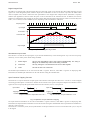
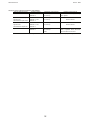
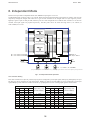
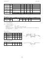
1
32-bit General Purpose I/O Interface IC
PIX132
User’s Manual
2005-9-08
2012-2-20
Ver. 1.0
Ver. 2.1
NOVA electronics
PIX132 - M2
NOVA electronics
Introduction
Before using the PIX132, please read this manual thoroughly to ensure correct usage according to specifications such as signal
voltage, signal timing, and operational parameter values.
In general, semiconductor products can malfunction or fail to function. Therefore, when incorporating this IC into a system,
ensure that a safety system is designed to prevent injury or damage to property caused by any malfunctioning of this IC.
The PIX132 is designed for application to general electronic devices such as industrial automation and robotics, measurement
instruments, computers, office equipment, household electrical goods, and so on. This IC is not intended for use in
high-performance, high-reliability equipment where failure or malfunctioning may directly cause death or injuries (atomic
energy control equipment, aerospace equipment, transportation equipment, medical equipment and various safety devices) and
operations for such uses cannot be guaranteed. The customer shall be solely responsible for the use of this IC in any such
high-performance and high-reliability equipment.
Notes on independent mode:
Before using in independent mode, make sure that INTN/TEST signals (14 pins) are short-circuited to GND. Keeping them open
can cause malfunction due to running internal test circuits on this IC.
2
PIX132 - M3
NOVA electronics
1. Outline
6
2. How to Operate PIX132
12
2.1.
General Input/Output Operation
12
2.2.
Simultaneous Input Latch
12
2.3.
Input Transition Trapping Function
13
2.4.
Simultaneous Output Set
14
2.5.
Bit Control Output
14
2.6.
Built-in Timer
15
2.7.
Interrupt Generation
15
2.8.
Status at Reset
15
3. Pin Assignments and Signal Description
16
3.1.
Pin Assignments
16
3.2.
Signal Description
17
3.3.
Input/ Output Circuit
19
3.4.
Notes for Design Circuitry
19
4. Register
20
4.1.
WR0 Register
-----------
Command Execution / Bit Control Output: 0
20
4.2.
WR1 Register
-----------
Bit Control Output: 1
21
4.3.
WR2,3 Register
Data Writing
21
4.4.
WR4,5,6,7 Register
4.5.
RR1 Register
4.6.
RR2,3 Register
4.7.
RR4,5,6,7 Register
------------
Port Output Value Setting
-------------------------
Display of Interrupt Request Factor
22
Display of Reading Data
23
Display of Real-time Input/Latch Input/Output/Input Transition
5. Commands
5.1.
22
23
25
26
Commands for Data Writing
3
PIX132 - M4
NOVA electronics
5.1.1.
5.1.2.
5.1.3.
5.1.4.
5.1.5.
5.1.6.
5.1.7.
5.1.8.
5.1.9.
5.2.
26
26
27
28
29
29
29
30
30
33
Commands for Reading Data
5.2.1.
5.2.2.
5.2.3.
5.3.
Input/Output Designation and Logical Setting
Input Filter Designation
Filter Time Constant Setting
Timer Value Setting
PAB Input Transition Enabling Setting
PCD Input Transition Enabling Setting
PAB Input Transition Direction Setting
PCD Input Transition Direction Setting
Action Mode / Interrupt Setting
Reading Setting Data
Read Register Display Status Reading
Activated Timer Value Reading
33
33
34
35
Other Commands
5.3.1.
5.3.2.
5.3.3.
5.3.4.
5.3.5.
5.3.6.
5.3.7.
5.3.8.
5.3.9.
5.3.10.
5.3.11.
5.3.12.
Timer Single Activation
Timer Continuous Activation
Timer Stop
Timer Cycle Stop
Input Transition Information Clear
Read Register Display Selecting 1
Read Register Display Selecting 2
Read Register Display Selecting 3
Read Register Display Selecting 4
Read Register Display Selecting 5
Simultaneous Input Latch
Simultaneous Output Set
----------------
Real-time Input + Output
Real-time Input
Latch Input
Output
Input Transition
35
35
35
35
35
36
36
36
36
37
37
37
6. Independent Mode
38
7. Examples
40
7.1.
Connection Example for the CPU
40
7.2.
Example Program
40
7.3.
Connection Example for Independent Mode
43
8. Electrical Characteristics
44
8.1.
DC Characteristics
44
8.2.
AC Characteristics
45
8.2.1.
8.2.2.
8.2.3.
8.2.4.
8.2.5.
8.2.6.
8.2.7.
8.2.8.
8.2.9.
8.2.10.
Measuring Condition
Clock
Reset Signal Width
CPU Read/ Write Cycle
Port Input Delay Time
Port Output Delay Time
Bit Control Output Delay Time
Strobe Signal Width
Simultaneous Input Latch Timing
Simultaneous Output Set Delay Time
45
45
45
46
47
47
47
47
48
48
4
PIX132 - M5
NOVA electronics
8.2.11 Interrupt Delay Time
8.2.12. Delay Time in Independent Mode
49
49
9. Package Dimensions
50
10. PIX132 Storage and Recommended Installation
Conditions
52
10.1 Storage of this IC
52
10.2 Standard Installation Conditions by Soldering Iron
52
10.3 Standard Installation Conditions by Solder Reflow
52
Appendix A
Clock Frequency Conversion Formula
53
Appendix B
Noise Removal of Built-in Integral Filter
54
5
PIX132 - M6
NOVA electronics
1. Outline
PIX132 is a 32-bit general purpose I/O interface IC equipped with a built-in digital integral filter. It can independently configure
input/output, input logic or filter time constant every 4-bit port. PIX132 provides various functions for output like bit control
output and simultaneous output set, with a single power supply within the 3.0 to 5.5V range so as to function on both 5V and
3.3V systems.
PIX132 has two operational modes as shown in Fig.1.1. The first is the CPU slave mode used in conjunction with the CPU bus
and the other is the independent mode where sixteen input ports are output through a built-in integral filter. When the IMODEN
input signal is set to Hi, the PIX132 operates in slave mode and when set to Low, it operates in independent mode.
Independent Mode
CPU Slave Mode
IMODEN = Hi
PIX132
CPU
PA
8-bit
PB
8-bit
PC
8-bit
PD
8-bit
IMODEN = Low
PIX132
8-bit
PA
8-bit
Note1
PB Integral Filter PD
PC
Output Enabler
Filter Time Constant Setting
Holding
Note1: In this figure, the integral filter is illustrated by
CR, but the signal is digitally processed in the IC.
Fig.1.1 Two Operational Modes of PIX132
Fig.1.2 shows the functional configuration in the IC when used in slave mode.
Time Constant 1 Time Constant 2 Time Constant 3
D[7:0]
A[2:0]
CSN
RDN
WRN
Data Bus
Buffer
CPU
Control
Command
Interpretation
and
Action Mode
INTN
Port A
High
4
PA[7:4]
Port A
Low
4
PA[3:0]
Port B
High
4
PB[7:4]
Port B
Low
4
PB[3:0]
Port C
High
4
PC[7:4]
Port C
Low
4
PC[3:0]
Port D
High
4
PD[7:4]
Port D
Low
4
PD[3:0]
Interrupt
Timmer
1μ ~32sec
Simultaneous
Output Buffer
Internal Data/Control Signal Bus
CLK(16MHz)
RESETN
VDD
IMODEN
Time Constant 1
Time Constant 2
Time Constant 3
1 μ ~32msec
1μ ~32msec
1 μ ~32msec
INSTB
OTSTB
INSTB :Simultaneous Input Latch Strobe
OTSTB :Simultaneous Output Latch Strobe
Fig.1.2 Internal Circuit Configuration in Slave Mode
6
PIX132 - M7
NOVA electronics
The PIX132 has 32 general purpose I/O signals, consisting of four 8-bit ports: Port A, Port B, Port C and Port D. Each 8-bit port
is divided into upper and lower 4-bit ports and these can be independently configured for input/output, selection of filter time
constant or input logic. The input signal is equipped with a built-in integral filter and each filter can select one time constant
from three types.
Fig.1.3 shows the reading and writing flow of input/output signals, taking as an example a PA0 signal, one of the 32-bit I/O
signals.
Reding Path of Input Signal
Real-time Input
Latch Input
logical
Setting
Latch
Reading Input Value
RR4/D0
Input
Transition
Differential
+ Latch
Output Value 0→1/1→0
Integral Filter
Hi:1/Low:1
Through
External
Time Constant 1
Signal
Command Time Constant 2
Timmer
Input/Output
Buffer
PA0
Output/Input
Time Constant 3
Writing Path of Output Signal
Register Data Writing
WR4/D0
Writing Output Value
Bit Control Output
WR0,1/Designated Number
Simultaneous
Output Buffer
Latch
Simultaneous Output
External
Signal
Command
Timmer
Fig.1.3 Reading and Writing path of input/output signals
Reading Flow of the Input Signal
As shown in Fig.1.3, first an input signal passes through an integral filter; a signal can be passed through without the filter. When
passing through the filter, the user can select one time constant from types 1, 2 and 3 which are each configurable for delay time
from 1μsec to 32msec. Every 4-bit port can be specified as to which time constant to be used. The signal passing the filter is set
to the logical level, where its level can be specified as Hi or Low to 1.
The CPU can attain the following information regarding logical input values:
①
Real-time Input Information about real-time input signals.
②
Latch Input
③
Input Transition Information about the transition of the specified input from 0 to 1 or 1 to 0.
Information about all inputs which are latched simultaneously by external latch
strobe signals, command writing from the CPU or the time-out of the timer.
The CPU reads these information inputs from RR4 to 7 registers. RR4~7 registers are 8-bit configurations respectively,
corresponding to RR4:PA[7:0], RR5:PB[7:0], RR6:PC[7:0], RR7:PD[7:0]. RR4~7 registers display not only with real-time
inputs but also latch inputs and input transition. These information inputs are switched by the command E5~E9h.
Output Signal Setting
As shown in Fig.1.3, output signals can be set by the following three ways when each I/O port is designated for output.
①
Register Data Writing
Writing output data in WR4, 5, 6 and 7 registers, output is set by the 8-bit
ports, PA, PB, PC and PD.
②
Bit Control Output
Writing the assigned number corresponding to the output signal, output is
set by a single bit.
③
Simultaneous Output
Writing output data in WR4, 5, 6 and 7 registers in advance, all outputs are
simultaneously set at the timing of external strobe signal, command writing
from the CPU and time-out of the timer.
7
PIX132 - M8
NOVA electronics
Digital Integral Filter
The PIX132 is equipped with a digital integral filter for each input signal of port PA~PD. This filter takes samplings of input
signal level at the designated period, and then outputs the accumulation of value to the back. It provides the function that
removes impulse noise, which is almost the same performance as the integral filter composed of RC (Resistance, Capacitor)
elements (See appendix B.) and can reduce the space on the circuit board for RC elements and cost. In addition, once the RC
elements are soldered, the time constant will be fixed. On the other hand, the built-in integral filter of this IC can alter delay time
from 1μsec to 32msec (at CLK=16MHz) any time, depending on the circumstances of the noise.
Sampling Period
Time
Input Si gnal
Acc umulation
Thres hold Level
Output Si gnal
Filter Delay Time
Fig.1.4 Operation of Digital Integral Filter
Simultaneous Input Latch
This function is to latch all the input signals of port PA~PD simultaneously in the following three ways. The user can specify
which way is to be used by action mode setting command.
①
Strobe Signal
Latch at the rising/falling edge of the external signal(INSTB). The rising or
falling can be selected by action mode setting command.
②
Command
Latch by writing the command EAh from CPU to WR0 register.
③
Timer
Latch at the time-out of the timer.
The latched input information can be read out from RR4~7 registers. However, when RR4~7 registers are displaying other
information, the latched input information can be read out after writing the command E7h.
Input Transition Trapping Function
This function is to trap the transition of input signals. The transition of the input value from 0 to 1 or from 1 to 0 can be trapped
concerning specified inputs. It is effective to monitor the rare transition of a signal or unexpected impulse noise that mixes with a
signal. The user can specify the signal and the direction of the transition (0 to 1/1 to 0) by the bit.
Input Value
0
1
Input Value
0
1
0
1
0
1
Trapping of
Trapping of
0
1
Transition
Transition
Trap the transition of input value from 0 to 1.
Trap the transition of input value from 1 to 0.
Fig.1.5 Operation of Input Transition Trapping
The input transition information can be read out from RR4~7 registers. However, when RR4~7 registers are displaying other
information, the input transition information can be read out after writing the command E9h. Once input transition information is
read out, it will be cleared.
This function is activated by clock (CLK) synchronization. If the input transition occurs in less time than CLK cycle, it may fail
to be trapped.
8
PIX132 - M9
NOVA electronics
Simultaneous Output Set
Normally writing the signal value (0:Low and 1:Hi) designated for output to WR4, 5, 6 and 7 registers will be set to each 8-bit
output port. Thus, as shown in Fig.1.6, when the user tries to set all of the ports PA~PD in the usual way, the output set is
delayed by each port, because a time difference occurs at the time of writing to each port, PA~PD from the CPU.
Writing PA output value
10101010
PA0
D-FF
WR4
PA7
PB0
Writing PB output value
Writing PC output value
11111111
01010101
WR5
D-FF
WR6
D-FF
Output PB7
Buffer PC0
PC7
PD0
Writing PD output value
11111111
D-FF
WR7
PD7
Delayed by each port.
Fig.1.6 Normal Output Set
This IC can perform to simultaneously set all of the output signals of each port, PA~PD by setting action mode. As shown in
Fig.1.7, if the simultaneous output mode is set, then the output data of port PA, which is written in WR4 register, is temporarily
latched and not outputted to port PA yet. Also values written in WR5, 6 and 7 registers are not reflected immediately and they are
temporarily latched.
Writing PA output value
Writing PB output value
Writing PC output value
10101010
11111111
01010101
WR4
WR5
WR6
Temporary
Latch
Temporary
Latch
Temporary
Latch
PA0
D-FF
PA7
PB0
D-FF
Output
PB7
Buffer PC0
D-FF
PC7
PD0
Writing PD output value
11111111
WR7
Temporary
Latch
D-FF
PD7
External Signal
All outputs are set simultaneously.
(OTSTB)
Writing the command EB
Command
Timer
Fig.1.7 Simultaneous Output Set
To output data simultaneously from output ports after writing output values in WR4, 5, 6 and 7 registers, there are the following
three ways:
①
Strobe Signal
Output at the rising/falling edge of the external signals (OTSTB). The
rising or falling can be selected by action mode setting command.
②
Command
Output by writing the command EBh from CPU to WR0 register.
③
Timer
Output at the time-out of the timer.
[Note] In a customer system, when the user tries to control switching on/off of a large current simultaneously with this function,
it is necessary to take preventive measures that minimize the voltage fluctuation of GND/Power or Cross-talk between the
signals which are generated by simultaneous switching of a large current.
9
PIX132 - M10
NOVA electronics
Bit Control Output
This function is to set an output signal by a single bit. In the ususal way, the output set is performed by writing to WR4, 5, 6 and
7 registers, so that signals are set to each 8-bit port. Therefore, when the user tries to set one specified output signal to Hi or Low
level, the user first must set the specified bit of 8-bit output data to 1OR or 0AND, then write it to the register. This IC does not
need such a burdensome operation. As shown in Fig.1.8, to set one specified signal to Low level, write the designation number
for the signal to WR0 register, then the signal will be set to Low or write the designation numbert for the signal to WR1 register,
then the signal will be set to Hi.
PA0
D-FF
Set 1 ×8
①Set PD0 signal to Low.
18h
WR0
②Set PA7 signal to Hi.
07h
WR1
D-FF
×8
D-FF
×8
PA7
PB0
Hi
Output PB7
Buffer PC0
Set 0 D-FF
×8
PC7
PD0
Low
PD7
Fig.1.8 Example of Bit Control Output
Interrupt Generation
The interrupt signal can be generated by input transition, external strobe and the timer.
Input Transition
Interrupt can be generated at the transition of the specified input signal
from 0 to 1 or 1 to 0 (selectable) concerning all the input signals.
External Strobe
Interrupt can be generated at the transition of external strobe signal
(INSTB) for simultaneous input latch or external strobe signal (OTSTB) for
simultaneous output set. The CPU can efficiently control because of no
need to wait for these signals.
Timer
Timer can be configured within the range from 1μsec to 32sec.
Interrupt can be generated at the time-out of the timer.
Reading Setting Value
Configuration such as input/output settings, logical settings, filter settings, output data or all setting data set by the CPU can be
read out. The current setting data can be read any time so that the CPU does not need to separately keep such output data even
when bit control output is performed.
10
PIX132 - M11
NOVA electronics
Independent Mode Operation
Independent mode is the operation mode that mainly uses only the integral filter function of this IC and does not connect this IC
to the CPU bus. Fixed 16 bit inputs are output to fixed output signals through the integral filter.
The filter time constant can be set to 4-bit of PA[3:0], 4-bit of PA[7:4] and 8-bit of PB[7:0] respectively. And each delay time of
the time constants can be externally designated within the range from 1μsec to 32msec.
PIX132
4 input signals
PA[3:0]
PC[3:0]
4 input signals
PA[7:4]
8 input signals
PB[7:0]
PC[7:4]
Integral Filter
PD[7:0]
PA[7:4] Time Constant Setting
PA[3:0] Time Constant Setting
PB Time Constant Setting
Fig.1.9 PIX132 Independent Mode
Note1: In this figure, the integral filter is illustrated by
CR, but the signal is digitally processed in the IC.
In addition, the signal for filter enable/disable, output signal holding and output signal enabling (enable/high impedance) are
prepared.
11
PIX132 - M12
NOVA electronics
2. How to Operate PIX132
2.1.
General Input/Output Operation
This chapter shows the user how to operate PIX132 in slave mode which is used in conjunction with the CPU bus. PIX132 has
four 8-bit ports, port PA, PB, PC and PD. Each 8-bit port is divided into upper and lower 4-bit ports and these 4-bit ports can be
independently configured input/output, input logic or filter. The operating procedures, such as configuration of each port, input
reading and output set, are shown as follows:
(1) Input/Output and Input Logical Setting
Configure each port whether to be used as input or output. When used as input,
input logic is also configured either Hi or Low to 1.
Reference
5.1
Commands for Data Writing
5.1.1 Input/Output and Input Logical
Page
26
26
Setting
(2) Input Filter Designation
Concerning the port configured as input, the user specifies whether to
pass through the integral filter or not. In the case of using the integral filter, the
user can select one time constant from three types.
(3) Filter Time Constant Setting
Configure the time constant of the integral filter of this IC. There are three
types of time constants 1, 2 and 3. Each time constant can configure the delay
time within the range from 1μsec to 32msec.
(4) Input Reading
Switch RR4, 5, 6 and 7 registers to a display “Real-Time Input” by writing
Read Register Display Selecting 2 command (E6h).
Reading RR4, 5, 6 and 7 registers corresponding to each port, the current input
signal status (the input value configured logical setting after passing the filter)
is available.
(5) Output Set
When the port is configured as output, output signals can be set by writing the
data in WR4, 5, 6 and 7 registers.
To read out the output data currently set, write Read Register Display Selecting
4 command (E8h) and then switch RR4, 5, 6 and 7 registers to a display
“Output”.
2.2.
Reference
Page
5.1
Commands for Data Writing
26
5.1.2
Filter Time Constant Setting
27
Reference
Page
5.1
Commands for Data Writing
26
5.1.3
Filter Time Constant Setting
27
Reference
5.3.7 Read Register Display
Selecting 2
4.7
RR4,5,6,7 Register
4.4
WR4,5,6,7 Register
Reference
5.3.9 Read Register Display
Selecting 4
4.7
RR4,5,6,7 Register
Page
36
23
Page
22
36
23
Simultaneous Input Latch
This function is to latch all the input signals of port PA~PD simultaneously. To latch simultaneously, there are three ways: strobe
signal, commands and the timer. The user can specify which way is to be used by action mode/interrupt setting command.
(1) Latch by Strobe Signal or Commands
To perform simultaneous input latch by strobe signal (INSTB) or commands, set 1 to WR2/D2 bit by action mode/interrupt
setting command and then specify whether to use the rising edge or falling edge of the strobe signal (INSTB) by WR2/D5 bit.
All the signals (the input value after passing through the filter) configured as
input are latched by the transition of INSTB signal or can be latched by writing
Simultaneous Input Latch Command (EAh). Simultaneous input latch data will
be kept until next transition of INSTB signal or simultaneous input latch
command (EAh) are written.
Reference
Page
5.1.9 Action Mode/Interrupt Setting
30
5.3.11 Simultaneous Input Latch
37
If WR3/D1 bit is set to 1 by action mode/interrupt setting command, an interruption can be generated by the transition of INSTB
signal.
12
PIX132 - M13
NOVA electronics
[Note1] Depending on the level of the INSTB signal, data may be latched at the writing of action mode/interrupt setting
command (C8h). For instance, when INSTB signal goes Hi and action mode/interrupt setting command (C8h) is written at the
rising edge, data will also be latched at the time of the command writing.
[Note2] After latched by the transition of the INSTB signal, the next latch is not performed for a maximum of 4CLK cycles even
though INSTB signal alters.
(2) Latch by Timer
PIX132 is equipped with a built-in timer which can set within the range from 1μsec to 32sec. All the input signals are
simultaneously latched at the time-out of the timer. The timer can be operated by single activation command or continuous
activation command which repeatedly operates until the CPU stops it. In continuous activation command, Input values are
latched every time-out. The procedures for simultaneous input latch by the timer are shown as follows:
① Set 1 to WR2/D3 bit by mode/interrupt setting command. Also set 1 to
WR3/D0 bit if you need to generate the interrupt by the time-out.
② Set the timer value.
③ Activate the timer by single activation command or continuous activation
command.
④ Confirm the time-out by reading the activated timer value or the interrupt
generation. When confirming by the interrupt generation, the user can
validate the interruption from the timer by RR1/D0 bit. INTN signal will
be released by reading RR1/D0 = 1.
(3) Reading Latched Input Value
Latched input value can be read from RR4, 5, 6 and 7 registers. At this time,
RR4, 5, 6 and 7 registers should display “Latch Input”, so write Read Register
Display Selecting 3 Command (E7h) in advance to switch RR4, 5, 6 and 7
registers to a display “Latch Input”.
2.3.
Reference
Page
5.1.9 Action Mode/Interrupt Setting
30
5.1.4 Timer Value Setting
28
5.3.1 Timer Single Activation
35
5.3.2 Timer Continuous Activation
35
5.2.3 Activated Timer Value Reading
34
4.5
22
RR1 Register
Reference
5.3.8 Read Register Display
Selecting 3
4.7
RR4,5,6,7 Register
Page
36
23
Input Transition Trapping Function
This function is to trap the transition of input signals concerning all of the input signals.
(1) Setting
Configure whether to enable or disable the transition trapping function and
specify the direction of the transition whether to trap the input value from 0 to
1 or from 1 to 0 for each input signal.
Enable/Disable can be set by PAB Input Transition Enabling Command or PCD
Input Transition Enabling Command. And the direction of the transition can be
set by PAB Input Transition Direction Command or PCD Input Transition
Direction Command.
Reference
5.1.5 PAB Input Transition Enabling
Setting
5.1.6 PCD Input Transition Enabling
Setting
5.1.7 PAB Input Transition Direction
Setting
5.1.8 PCD Input Transition Direction
Setting
Page
29
29
29
30
(2) Transition Trapping Behavior
Regarding the signal enabled by Input Transition Enabling Command, the transition trapping function is immediately operated.
When an input value goes to the specified direction, the input transition becomes “1”. This “1” is kept until the register
corresponding to the input signal is read out even though the transition of the input signal occurs repeatedly.
(3) Reading Input Transition
Input transition information can be read from RR4, 5, 6, and 7 registers. At this
time, RR4, 5, 6 and 7 registers should display “Input Transition”, so write Read
Register Display Selecting 5 Command(E9h) in advance to switch RR4, 5, 6
and 7 registers to a display “Input Transition”.
Input transition information will be cleared once read out.
(4) Clearing Transition Information
Input transition information of each register is cleared by reading RR4~7
registers. Or it can be cleared for all the registers by command.
Reference
5.3.10 Read Register Display
Selecting 5
4.7
RR4,5,6,7 Register
Reference
5.3.5 Input Transition Information
Clear
Page
37
23
Page
35
[Note] This function is activated by clock (CLK) synchronization. Even without the filter, if the input transition occurs in less
time than CLK cycle, it may fail to be trapped.
13
PIX132 - M14
NOVA electronics
2.4.
Simultaneous Output Set
This function is to set all of the output signals in PA~PD ports simultaneously. To set the output simultaneously, there are three
ways: strobe signal, commands and the timer. The user can specify which way is to be used by action mode/interrupt setting
command.
(1) Simultaneous Output by Strobe Signal or Commands
To perform simultaneous output set by a strobe signal (OTSTB) or commands, set 1 to WR2/D0(Simultaneous Output 1) bit by
action mode/interrupt setting command, and specify either the rising edge or falling edge of the strobe signal (OTSTB) by
WR2/D4 bit.
If WR2/D0(Simultaneous Output 1) bit is set to 1 and action mode/interrupt
Reference
Page
setting command is written, then output signals cannot be changed by writing
5.1.9 Action Mode/Interrupt Setting
30
the output value in WR4, 5, 6 and 7 registers. Write the output value to all of
5.3.12 Simultaneous Output Set
37
WR4, 5, 6 and 7 registers and then make the strobe signal (OTSTB) change or
4.4 WR4,5,6,7 Register
22
write simultaneous output set command, all the output signals will be set
simultaneously.
If WR3/D2 bit is set to 1 by action mode/interrupt setting command, interrupt can be generated at the transition of the OTSTB
signal.
(2) Simultaneous Output Set by Timer
PIX132 is equipped with a built-in timer which can set within the range from 1μsec to 32sec. Activating the timer, the user can
simultaneously output the output values already written in WR4, 5, 6 and 7 registers at the time-out of the timer. There are two
modes of timer behavior, single activation which works only once and continuous activation which repeatedly operates until the
CPU stops it. In continuous activation, output values written in WR4, 5, 6 and 7 registers are simultaneously output every
time-out. The procedures of simultaneous output set by the timer are shown as follows:
① Set 1 to WR2/D1 bit by mode/interrupt setting command. Also set 1 to
WR3/D0 bit if you need to generate the interrupt by the time-out.
Reference
Page
② Set the timer value.
5.1.9 Action Mode/Interrupt Setting
30
③ Write output values in WR4, 5, 6 and 7 registers.
5.1.4 Timer Value Setting
28
④ Activate the timer by single activation command or continuous activation
5.3.1 Timer Single Activation
35
command.
5.3.2 Timer Continuous Activation
35
⑤ Confirm the time-out by reading the activated timer value or the interrupt
5.2.3 Activated Timer Value Reading
34
generation. Output signals are set at the time-out.
4.4 WR4,5,6,7 Register
22
⑥ With the interrupt generation, the user can validate the interruption from
the timer by RR1/D0 bit. INTN signal will be released by reading RR1/D0 = 1.
⑦ When the timer is activated in continuous activation, write next output values in WR4, 5, 6 and 7 registers and then repeat
⑤ to ⑥.
Notes on Simultaneous Output Set:
● Output Port Capacitance Load
Please do not set the capacitance load over 50pF per output port to all the outputs simultaneously, as an operation error may
occur. In such a case, place the driver IC after the output port.
● Preventive measures for Simultaneous Switching
In a customer system, when the user tries to control switching on/off of a large current in the back step of this IC using the
simultaneous output set function, it is necessary to take preventive measures that minimize the voltage fluctuation of
GND/Power or Cross-Talk between the signals whch are generated by simultaneous switching of a large current.
● Delay in Port PA, PD
To avoid malfunction by simultaneous switching in the IC, outputs of ports PA, PD are delayed about 7nsec (VDD=5V typ.
value) from those of ports PB, PC. See section 8.2.9.
2.5.
Bit Control Output
Reference
This function is to set an output signal by a single bit. When the user tries to set
4.1 WR0 Register
a specified output signal to Low level, write the designation number for the
4.2 WR1 Register
signal to WR0 register, then the signal will be set to Low. And write the
designation number for the signal to WR1 register, then the corresponding signal will be set to Hi.
14
Page
20
21
PIX132 - M15
NOVA electronics
2.6.
Built-in Timer
PIX132 is equipped with a built-in timer which can set within the range from 1μsec to 32sec. The following three operations
can be performed at the time-out of the timer. Please refer to each section.
・
Simultaneous Input Latch
Section 2.2
・
Simultaneous Output Set
Section 2.4
・
Interrupt Generation
Section 2.7
Procedures to activate the timer are shown as follows:
① Set the timer value.
② If you need to generate the interrupt by the time-out, set 1 to WR3/D0 bit
by mode/interrupt setting command.
③ Activate the timer by single activation command or continuous activation
command.
④ To stop the single activated timer, write Timer Stop Command. And to
stop the continuous activated timer, write Timer Stop Command or Timer
Cycle Stop Command.
2.7.
Reference
Page
5.1.9 Action Mode/Interrupt Setting
30
5.1.4 Timer Value Setting
28
5.3.1 Timer Single Activation
35
5.3.2 Timer Continuous Activation
35
5.3.3 Timer Stop
35
5.3.4 Timer Cycle Stop
35
5.2.3 Activated Timer Counter Value
Reading
34
Interrupt Generation
This IC has an interrupt output signal (INTN) to the CPU. The INTN signal is the open drain output so that it is necessary to pull
up to the VDD through resistance. Interrupt can be generated by the following four operations. To enable each interrupt
generation, specify it by action mode/interrupt setting command.
・
・
・
・
2.8.
Time-out of the timer
Transition of INSTB signal at the simultaneous input latch
Transition of OTSTB signal at the simultaneous output set
Input Transition
Reference
Page
5.1.9 Action Mode/Interrupt Setting
30
Status at Reset
At resetting, each configurable operation in slave mode of this IC is shown as follows:
Operation
Status at Reset
Port PA~PD Input/Output
All the signals are Input.
Designation of Input/Output
Port PA~PD Input Logic
All the signals are 0. (Hi to 1)
and Logical Setting.
Port PA~PD Filter Designation
All the signals are without filter.
Input Filter Designation
Filter Time Constant 1, 2, 3
All of 1, 2, 3 is 0. (Delay Time 1
μ)
Related Commands
Filter Time Constant Setting
Timer Value
0
Timer Value Setting
PAB, PCD Input Transition
All the signals are disabled.
PAB, PCD Input Transition
Enabling/Disabling
PAB, PCD Input Transition Direction
Enabling Setting
All the signals are 0. (Transition of
input value from 0 to 1.)
Simultaneous Output 1
PAB, PCD Input Transition
Direction Setting
Disable
(Strobe/Commands)
Simultaneous Output 2 (Timer)
Disable
Simultaneous Input Latch 1
Disable
(Strobe/Commands)
Simultaneous Input Latch 2(Timer)
Disable
OTSTB Direction
0 (the rising edge)
INSTB Direction
0 (the rising edge)
Interrupt by Timer
Disable
Interrupt by Simultaneous Input Latch
Disable
INSTB Signal
Interrupt by Simultaneous Output OTSTB
Disable
Signal
Interrupt by Input Transition
Disable
15
Action Mode/Interrupt Setting
PIX132 - M16
NOVA electronics
3. Pin Assignments and Signal Description
48
47
46
45
44
43
42
41
40
39
38
37
36
35
34
33
PA6
PA7
PB0
PB1
PB2
PB3
PB4
PB5
GND
VDD
PB6
PB7
PC0
PC1
PC2
PC3
Pin Assignments
49
50
51
52
53
54
55
56
57
58
59
60
61
62
63
64
NOVA elec.
P IX132
Index Mark
Glossy circle
32
31
30
29
28
27
26
25
24
23
22
21
20
19
18
17
GND
VDD
PC4
PC5
PC6
PC7
PD0
PD1
PD2
GND
VDD
PD3
PD4
PD5
PD6
PD7
1
2
3
4
5
6
7
8
9
10
11
12
13
14
15
16
VDD
GND
PA5
PA4
PA3
PA2
PA1
PA0
GND
CLK
VDD
IMODEN
D7/PAHF3
D6/PAHF2
D5/PAHF1
D4/PAHF0
D3/PALF3
D2/PALF2
D1/PALF1
D0/PALF0
VDD
RESETN
GND
A2/PBF2
A1/PBF1
A0/PBF0
CSN/PBF3
WRN/PAFE
RDN/PBFE
INTN/TEST
INSTB/HLDN
OTSTB/OEN
3.1.
・ 64 pin TQFP package, external package: 12×12mm, lead pitch: 0.5mm, lead free
・ See Chapter 9 for the package dimensions.
16
PIX132 - M17
NOVA electronics
3.2.
Signal Description
Pin
Number
Input/Output
CLK
58
Input A
D0/PALF0
D1/PALF1
D2/PALF2
4
3
2
Bi-directional A
Bi-directional A
Bi-directional A
D3/PALF3
1
Bi-directional A
D4/PAHF0
D5/PAHF1
D6/PAHF2
64
63
62
Bi-directional A
Bi-directional A
Bi-directional A
D7/PAHF3
61
Bi-directional A
A0/PBF0
A1/PBF1
10
9
Input A
Input A
A2/PBF2
8
Input A
CSN/PBF3
11
Input A
WRN/PAFE
12
Input A
RDN/PBFE
13
Input A
RESETN
6
Input A
Signal Name
See section 3.3 for Input/Output in the table.
Signal Description
Slave Mode
Independent Mode
Clock: clock signal for internal synchronous circuits of PIX132.
The standard frequency is 16MHz, which the filter time constant or
timer value is based upon. If the frequency setting is not 16MHz,
the filter time constant or timer value will differ.
D0 ~ D7 Data Bus: 3-state PALF0~3: signals for PA lower
bi-directional 8-bit data bus, 4-bit (PA0~3) inputs to set the
used in conjunction with system time constant of an integral
data bus. D7 is the highest filter. PALF3 is the highest
signal and D0 is the lowest signal and PALF0 is the lowest
signal. Low is 0 and Hi is 1. signal. Low is 0 and Hi is 1.
When CSN is Low and RDN is PAHF0 ~ 3: signals for PA
Low, these signals are for upper 4-bit (PA4~7) inputs to
outputting.
set of the time constant of an
integral filter. PAHF3 is the
highest signal and PAHF0 is
the lowest signal. Low is 0 and
Hi is 1.
A0 ~ A2 Address: address PBF0~3: signals for port PB
signals for host CPU to access (PB0~7) inputs to set the time
the read /write registers. A2 is constant of an integral filter.
the highest signal and A0 is the PBF3 is the highest signal and
lowest signal.
PBF0 is the lowest signal. Low
Low is 0 and Hi is 1.
is 0 and Hi is 1.
Chip Select: input signal for
[Note] Please note that the
selecting PIX132 as I/O device.
Set Low level for data reading pins for PBF3~0 are not in
sequence.
and writing.
Write Strobe: set Low when data PA Filter Enable: signal to
is written in the write registers. enable the integral filter of PA
When WRN is Low, CSN and input. Hi is enable and Low is
A2~A0 must be valid. When disable. When it is disabled, PA
WRN is up (↑), the data will be input is directly output to port
latched in the write register. PC without the filter.
D7~D0 should be valid before or
after WRN up (↑).
Read Strobe: set Low when data PB Filter Enable: signal to
is read out from the read enable the integral filter of PB
register. When CSN is set to input. Hi is enable and Low is
Low and RDN is set to Low, the disable. When it is disabled,
data of the read register PB input is directly output to
selected by A2~A0 address port PD without the filter.
signal is output to the data bus
during RDN Low.
Reset: reset (initialize) signal for Reset: reset (initialize) signal
PIX132. Setting to Low, PIX132 for PIX132. When RESETN
will be reset. Power-on reset by signal is Low, outputs of port
RESETN signal is necessary. PC, PD will be Low regardless
After PIX132 has been reset, all of input signals of port PA, PB.
of the ports of PA~PD will be
input. And all of mode settings
are also initialized. See section
2.8.
17
PIX132 - M18
NOVA electronics
Signal Name
INTN/TEST
IMODEN
PA7~PA0
PB7~PB0
PC7~PC0
PD7~PD0
Pin
Number
Input/Output
14
Bi-directional A
60
47,48,51,
52,
53,54,55,
56
37,38,41,
42,
43,44,45,
46
27,28,29,
30,
33,34,35,
36
17,18,19,
20,
21,24,25,
26
INSTB/HLD
N
15
OTSTB/OEN
16
VDD
5,22,31,
39,49,59
GND
7,23,32,
40,50,57
Input A
Bi-directional A
Bi-directional A
Bi-directional A
Bi-directional A
Input A
Bi-directional B
(uses input only)
Signal Description
Slave Mode
Independent Mode
Interrupt:
output
signal
of Test: input signal for testing
interrupt request for host CPU. If the internal circuits. When in
the interrupt is generated by any independent
mode
interrupt
factor,
INTN
will (IMODEN=Low), this signal
become Low. After the interrupt must be connected to GND, or
is released, it will return to Hi-Z the internal test circuits will be
level.
activated.
Independent Mode: Set Low (connect to GND) when PIX132 is
operated in independent mode. And set Hi (connect to VDD) when
PIX132 is operated in CPU slave mode.
Port A: PA, 8-bit I/O ports.
PA, 8-bit input ports.
Upper 4-bit and lower 4-bit can These are for input only.
be independently configured
input/output by mode setting.
Port B: PB, 8-bit I/O ports.
PB, 8-bit input ports
Upper 4-bit and lower 4-bit can These are for input only.
be independently configured
input/output by mode setting.
Port C: PC, 8-bit I/O ports.
PC, 8-bit output ports.
Upper 4-bit and lower 4-bit can PA input signal is output
be independently configured through an integral filter.
input/output by mode setting.
Port D: PD, 8-bit I/O ports.
PD, 8-bit output ports.
Upper 4-bit and lower 4-bit can PB input signal is output
be independently configured through an integral filter.
input/output by mode setting.
Input Latch Strobe: strobe pulse Hold: hold the output of ports
to latch PA~PD inputs. Mode PC, PD. This signal is low
setting is necessary to function level to hold the port PC, PD.
this.
Output Latch Strobe: strobe Output Enable: signal to
pulse input for PA~PD outputs enable PC, PD output ports.
to simultaneously output. Mode When this signal is low, PC,
setting is necessary to function PD output signals will be
this.
enabled. And when Hi, they wll
be high impedance.
+5V(or +3.3V) Power Terminal.
All of the 6 pins must be connected to the power pattern on the
substrate.
Ground 0V Terminal.
All of 6 pins must be connected to the ground pattern on the
substrate.
18
PIX132 - M19
NOVA electronics
3.3.
Input/ Output Circuit
Input A
Bi-directional
A
Bi-directional
B
3.4.
More than 10kΩ~hundreds of kilo impedance is for internal impedance, which can pull up the
VDD to the TTL Level input of a Smith trigger.
CMOS and TTL can be connected.
The user should open or pull up to VDD if the input is not used.
Input side is TTL Smith trigger, which is high impedance because it is not pulled up with high
resistance in the IC. Pull up signals, which are not used, with high resistance to VDD or pull
down to GND. Concerning data signals (D7~D0), the user should pull up the data bus with high
resistance for signal line not to attain high impedance.
Output side is CMOS level output, 8mA driving buffer at VDD=5V (High level output current
IOH=-8mA, VOH=2.4Vmin, Low level output current IOL=8mA, VOL=0.4Vmax) and 4mA driving
buffer at VDD=3.3V (Hi level output current IOH=-4mA, VOH=2.4Vmin, Low level output current
IOL=4mA, VOL=0.44Vmax).
The same circuit as bi-directional A but uses input only. Input side is TTL Smith trigger, which is
high impedance because it is not pulled up with high registance in the IC. When IMODEN is
Low (independent mode), INTN/TEST signal must be connected to GND, or the internal test
circuit will be activated and the OTSTB/OEN signal will be output.
Notes for Design Circuitry
Processing of GND, VDD Terminals
Make sure that all of GND and VDD terminals are each connected to the ground pattern and the power pattern on the substrate.
De-coupling Capacitor
Please connect VDD and GND with two to four De-coupling capacitors (about 0.1μF).
19
PIX132 - M20
NOVA electronics
4. Register
This chapter indicates to the user how to access all the registers in PIX132, and what the mapping addresses are of these
registers.
Both read and write registers have eight registers respectively and each register consists of 8-bit.
Writing/ Reading Operation
In order to write the data of the write register, select the register by A2~A0 signal, if CSN signal is Low and WRN signal is set
from Low to Hi, values of the data bus (D7~D0) will be written in the selected register. Also in order to read the data of the read
register, select the register by A2~A0 signal, if CSN signal is Low and RDN signal is set to Low, values of the read register will
be output to the data bus (D7~D0). For more details on read/ write timing, please refer to chapter 8.4.2.
■ Write Register
Address
A2
A1
A0
Symbol
Function
0
0
0
WR0
Command Execution, Bit Control Output: 0
0
0
1
WR1
Bit Control Output: 1
0
1
0
WR2
Data Writing (Lower)
0
1
1
WR3
Data Writing (Upper)
1
0
0
WR4
Port PA Output Value Setting
1
0
1
WR5
Port PB Output Value Setting
1
1
0
WR6
Port PC Output Value Setting
1
1
1
WR7
Port PD Output Value Setting
■ Read Register
Address
4.1.
A2
A1
A0
0
0
0
Symbol
RR0
Function
Not used
0
0
1
RR1
Display of Interrupt Request Factor
0
1
0
RR2
Display of Reading Data (Lower)
0
1
1
RR3
Display of Reading Data (Upper)
1
0
0
RR4
Port PA Display of Real-time Input, Latch Input, Output, Input Transition
1
0
1
RR5
Port PB Display of Real-time Input, Latch Input, Output, Input Transition
1
1
0
RR6
Port PC Display of Real-time Input, Latch Input, Output, Input Transition
1
1
1
RR7
Port PD Display of Real-time Input, Latch Input, Output, Input Transition
WR0 Register
-----------
Command Execution / Bit Control Output: 0
WR0 Register is used for the following two functions:
① Command Execution
Writing a value more than C0 (hex) to WR0 register, PIX132 takes it as a command and then the corresponding
command is executed. Please refer to chapter 5 for command execution.
② Bit Control Output: 0
The function for only one output signal to be set to low by writing the number corresponding to the output signal
to WR0 register. Write the signal designation number corresponding to the signal shown in the table to D4~D0 of
WR0 register, and the corresponding output signal will be low.
[Note] Bit control output: 0 is disabled when the simultaneous output is set (D0 or D1 by C8 command.).
20
PIX132 - M21
NOVA electronics
WR0
D7
D6
D5
0
0
0
D4
D3
D2
D1
D0
Bit Control Output: 0
(Output: Low)
Signal Designation Number
Signal Designation
Number
(HEX)
Signal Designation
Signal
Pin Number
Name
Signal
Number
Pin Number
Name
(HEX)
00
PA0
56
10
PC0
36
01
PA1
55
11
PC1
35
02
PA2
54
12
PC2
34
03
PA3
53
13
PC3
33
04
PA4
52
14
PC4
30
05
PA5
51
15
PC5
29
06
PA6
48
16
PC6
28
07
PA7
47
17
PC7
27
08
PB0
46
18
PD0
26
09
PB1
45
19
PD1
25
0A
PB2
44
1A
PD2
24
0B
PB3
43
1B
PD3
21
0C
PB4
42
1C
PD4
20
0D
PB5
41
1D
PD5
19
0E
PB6
38
1E
PD6
18
0F
PB7
37
1F
PD7
17
・ It will be disabled when the designation of the signal is not defined as output.
・ [Note] Set 0 to D7~5 bits of WR0 register, or unexpected commands may be executed.
4.2.
WR1 Register
-----------
Bit Control Output: 1
The function for only one output signal to be set to Hi by writing the number corresponding to the output signal to WR1 register.
Write the signal designation number corresponding to the signal shown in the table in section 4.1. to D4~D0 of WR1 register,
and the corresponding output signal will be Hi.
WR1
D7
D6
D5
0
0
0
D4
D3
D2
D1
D0
Bit Control Output: 1
(Output: Hi)
Signal Designation Number
[Note] Bit control output: 1 is disabled when simultaneous output is set (D0 or D1 by C8 command.).
4.3.
WR2,3 Register
---------
Data Writing
WR2, 3 registers are used to set the data of commands for data writing. Writing the command code to WR0 register after setting
the data to WR2, 3 registers, the contents of WR2, 3 registers will be taken to the IC. When the data is a 2-byte length, set
low-byte data to WR2 register and high-byte data to WR3 register. When the data is a 1-byte length, only set to WR2 register
with no need to set 0 to WR3 register.
D7
D6
D5
D4
D3
WR2
D2
D1
D0
Low-byte of Writing Data
21
PIX132 - M22
NOVA electronics
D7
D6
D5
D4
D3
D2
D1
D0
WR3
4.4.
WR4,5,6,7 Register
High-byte of Writing Data
----
Port Output Value Setting
These registers are configurable output values of each port PA, PB, PC and PD. Low can be set to 0 to the corresponding bit of
each signal and Hi to 1 as well. If the user only sets each half of the port to output mode, either value (1 or 0) can be set to the
rest of signals configured as input mode. They are ignored.
D7
D6
D5
D4
D3
D2
D1
D0
WR4
PA7
PA6
PA5
PA4
PA3
PA2
PA1
PA0
D7
D6
D5
D4
D3
D2
D1
D0
WR5
PB7
PB6
PB5
PB4
PB3
PB2
PB1
PB0
D7
D6
D5
D4
D3
D2
D1
D0
WR6
PC7
PC6
PC5
PC4
PC3
PC2
PC1
PC0
D7
D6
D5
D4
D3
D2
D1
D0
WR7
PD7
PD6
PD5
PD4
PD3
PD2
PD1
PD0
Port PA Output Value Setting
0:Low 1:Hi
Port PB Output Value Setting
Port PC Output Value Setting
Port PD Output Value Setting
・ If the user enables simultaneous output 1, 2 (See action mode/interrupt setting command (C8h)), output does not alter
immediately after writing the value to WR4, 5, 6 and 7 registers.
・ When the user does not set the input/output of each signal to output mode by input/output designation command (C0h), data
will not output by writing to these registers.
4.5.
RR1 Register
------------
Display of Interrupt Request Factor
Displays the interrupt request factor (except for input transition). 1 indicates that is the interrupt request factor.
RR1
D7
D6
D5
D4
D3
D2
D1
D0
0
0
0
0
0
OTS
INS
TIM
1: Interrupt Request
D0
TIM
indicates the time-out of the timer. (timer count = the setting value).
When the timer is in continuous activation, timer count = at the setting value.
D1
INS
indicates the transition of INSTB signal.
D2
OTS
indicates the transition of OTSTB signal.
・ To generate the interrupt, the interrupt factor which is needed must be enabled by action mode/interrupt setting command
(C8h) in advance.
・ Once the CPU reads out, all the bits of RR1 register will be cleared.
22
PIX132 - M23
NOVA electronics
■ Common Interrupt Operation
When the interrupt factor enabled by action mode/interrupt setting command is generated, the INTN signal will go from Hi-Z to
Low level and 1 will be set to the proper bit of RR1 register. And after reading RR1 register during interrupt processing routine
in the CPU, the INTN output signal will return to Hi-Z and all the bits of RR1 register will be cleared to 0.
Next is the same too.
INSTB Input Signal
INTN Output Signal
RR1/D1 Value
Hi-Z
Low
0
1
RR1 Lead RDN
INSTB down (↓)
outputs INTN and
RR1/D1 will be 1.
RR1 reading releases
INTN output and RR
1 will be cleared.
■ In the case when next factor has been generated while reading RR1 register.
When the interrupt generation of each factor and the timing of reading from the CPU overlaps, the interrupt generation will be
held internally until reading is finished, so PIX132 does not miss next interrupt generation by reading.
INSTB Input Signal
INTN Output Signal
RR1/D1 Value
Kept low due to occurrence of next factor.
Hi-Z
Low
Low
0
1
1
RR1 Lead RDN
■ In the case when next factor has been generated ahead of reading RR1 register after an interruption occurred.
When the same factor has been generated again ahead of reading RR1 after an interruption occurs, this interrupt generation is
ignored.
This generation of the factor is ignored.
INSTB Input Signal
INTN Output Signal
RR1/D1 Value
Hi-Z
Low
0
1
RR1 Lead RDN
4.6.
RR2,3 Register
----------
Display of Reading Data
RR2, 3 resigsters are used to set the data of commands for reading data. Writing the command code to WR0 register, the data
corresponding to the command will be set from the internal circuits to RR2, 3 registers. When the data is a 2-byte length,
low-byte data will be set to RR2 register and high-byte data will be set to RR3 register. When the data is a 1-byte length, data
will be set to RR2 register and 0 will be set to RR3 register.
D7
D6
D5
D4
D3
D2
D1
D0
RR2
Low-byte of Reading Data
D7
D6
D5
D4
D3
RR3
4.7.
RR4,5,6,7 Register
D2
D1
D0
High-byte of Reading Data
-----
Display of Real-time Input/Latch Input/Output/Input Transition
RR4, 5, 6 and 7 registers are used to display input values of ports, PA, PB, PC and PD respectively. Each register corresponds to
RR4:PA[7:0], RR5:PB[7:0], RR6:PC[7:0] and RR7:PD[7:0].
23
PIX132 - M24
NOVA electronics
RR4
D7
D6
D5
D4
D3
D2
D1
D0
PA7
PA6
PA5
PA4
PA3
PA2
PA1
PA0
D7
D6
D5
D4
D3
D2
D1
D0
RR5
PB7
PB6
PB5
PB4
PB3
PB2
PB1
PB0
D7
D6
D5
D4
D3
D2
D1
D0
RR6
PC7
PC6
PC5
PC4
PC3
PC2
PC1
PC0
D7
D6
D5
D4
D3
D2
D1
D0
RR7
PD7
PD6
PD5
PD4
PD3
PD2
PD1
PD0
Port PA
Port PB
Port PC
Port PD
RR4, 5, 6 and 7 registers also display not only real-time input (current input value) but latch input, input transition and current
output value. This displayed information can be switched by E5 to E9h commands.
Displayed Information
Contents
Command for
Bit (1, 0) Description
Selecting Display
Real-time Input
Displays input value which passed an
integral filter.
Latch Input
Displays latched input value which passed
an integral filter. Note1
Output
Displays the status of the output signal
currently set.
Input Transition
E6
E7
E8
Displays input transition. Note2
Information of input transition will be cleared
Depends
on
input
logic
on
input
logic
setting.
Depends
setting.
0:Low level
1:Hi level
0:No transition
E9
1:Transition occured
once it is read out.
Real-time Input +
Displays real-time input when the signal is
Output
set to input mode and displays output value
See above.
E5
when the signal is set to output mode.
[Note1] Latch is performed by any of the three, external signal (INSTB), command (EAh) or the timer.
[Note2] It is necessary to enable input transition trapping and set the direction of transition in advance.
The user does not need to write commands for selecting display every reading of the input value. Once the commands for
selecting display are written, they are valid until next commands for selecting display are written.
The user can confirm the current displayed information of each RR4, 5, 6 and 7 registers. Writing commands for reading data
(D9h) of read register display status, the user can read the current selection from RR2 register. For more details, see chapter
5.2.2.
24
PIX132 - M25
NOVA electronics
5. Commands
Commands for PIX132 are classified into three groups: commands for data writing, commands for reading data and other
commands.
Commands for data writing can be performed by writing the command code to WR0 after writing the data in WR2 and WR3.
WR2 is for low-byte data and WR3 is for high-byte data. If the data is a 1-byte length, the user only writes in WR2 and no need
to write 0 in WR3.
Commands for reading data can be performed by writing the command code to WR0, which sets reading data to RR2, 3. If the
data is a 1-byte length, the data will be set to RR2 register and RR3 (high-byte) will be 0.
Other commands can be performed by writing the command code to WR0.
Group
Code
C0
Command
Input/output designation and logical setting
Writing
Reading
Data Length
Data Length
(Byte)
(Byte)
2
Page
26
C1
Input filter designation
2
26
C2
Filter time constant setting
2
27
C3
Timer value setting
2
28
Data
C4
PAB Input transition enabling setting
2
29
Writing
C5
PCD Input transition enabling setting
2
29
C6
PAB Input transition direction setting
2
29
C7
PCD Input transition direction setting
2
30
C8
Action mode/interrupt setting
2
30
D0
Reading
Data
Input/output designation and logical setting
reading
2
D1
Input filter designation reading
2
D2
Setting filter time constant reading
2
D3
Setting timer value reading
2
D4
PAB Input transition enabling reading
2
33
D5
PCD Input transition enabling reading
2
D6
PAB Input transition direction reading
2
D7
PCD Input transition direction reading
2
D8
Action mode/interrupt setting reading
2
D9
Read register display status reading
1
33
DA
Activated timer value reading
2
34
E0
Timer single activation
35
E1
Timer continuous activation
35
E2
Timer stop
35
E3
Timer cycle stop
35
E4
Input transition information clear
35
Read register display selecting 1
36
E5
E6
Others
E7
E8
E9
(Real-time input + output)
Read register display selecting 2
36
(Real-time input)
Read register display selecting 3
36
(Latch input)
Read register display selecting 4
36
(Output)
Read register display selecting 5
37
(Input transition)
EA
Simultaneous input latch
37
EB
Simultaneous output set
37
25
PIX132 - M26
NOVA electronics
Notes for the timing of writing commands
This IC needs a time more than 2CLK cycles to proceed with the command. After writing the command in the IC, be sure to
access for the next one after taking a time interval of more than 2CLK cycles (When CLK=16MHz, it will be 125nsec).
Command Writing Next command Writing
Data Writing
Reading data command
Data Reading
RDN
WRN
D[7:0]
Data
Command
Command
2× tcyc and over
Reading data
Command
2× tcyc and over
2× tcyc and over
Fig.5.1 PIX132 Access Timing
5.1.
Commands for Data Writing
Commands for data writing can be executed by writing the command code to WR0 after writing the data to WR2, WR3. WR2 is
for low-byte data and WR3 is for high-byte data. If the data is a 1-byte length, the user only writes the data to WR2 and no need
to write 0 to WR3. This IC can read out all the data by commands for reading data which is set in the IC by commands for data
writing.
5.1.1.
Input/Output Designation and Logical Setting
Code
Command
C0
Input/Output Designation
and Logical Setting
Function
Input/output signals can be configured as input/output with each
4-bit port.
Logical level for input signals can be set for 4-bit ports
respectively.
Each port can be configured as input or output by setting D0~D7 bits of WR2 register, **H indicates upper 4-bit ports and **L
indicates lower 4-bit ports, and it is defined by 0: input and 1: output. For instance, when D0 is set to 0, ports PA3, PA2, PA1 and
PA0 will be configured as input and when D1 is set to 1, ports PA7, PA6, PA5 and PA4 will be configured as output. Also
concerning D2 to D7 bits, Port PB to PD can be configured as input/output by each 4-bit port.
Logical level of each input signal can be configured for 4-bit ports respectively. **H indicates upper 4-bit ports and **L
indicates lower 4-bit ports, and it is defined by 0: High of input signal to input value 1 and 1: Low of input signal to input value
1. It does not matter whether 0 or 1 is for the signals which are designated output. This selection of logical level does not
function for output.
WR2
D7
D6
D5
D4
D3
D2
D1
D0
PDH
PDL
PCH
PCL
PBH
PBL
PAH
PAL
0: Input
1: Output
Input/Output Designation
WR3
D7
D6
D5
D4
D3
D2
D1
D0
PDH
PDL
PCH
PCL
PBH
PBL
PAH
PAL
0: Hi to Input Value 1
1: Low to Input Value 1
Logical Setting of Input Signal
At resetting, all the ports will be input mode and Hi level of input signals will be input value 1.
5.1.2.
Input Filter Designation
Code
Command
C1
Input Filter Designation
Function
Specifies the time constant of the integral filter for input signals
26
PIX132 - M27
NOVA electronics
to each 4-bit input port.
Regarding all the input signals, the user can specify the filter time constant from three types for 4-bit ports respectively by WR2,
3 registers.
D7
D6
D5
D4
D3
D2
D1
D0
WR2
PBH
Designation
D7
PBL
Designation
D6
D5
PAH
Designation
D4
D3
D2
PAL
Designation
D1
D0
WR3
PDH
Designation
PDL
Designation
Designation Value
(Upper/Lower Bits)
0,0
0,1
1,0
1,1
PCH
Designation
PCL
Designation
Filter Behavior
Without filter
Set the filter time constant 1.
Set the filter time constant 2.
Set the filter time constant 3.
・ **H indicates upper 4-bit ports and **L indicates lower 4-bit ports.
・ Set 00 to the signal configured as output because its filter function does not work.
・ At resetting, all the input ports will be without filter.
[Notes on switching designation] While the filter is disabled, filter calculation of the IC stops so that input values before
disabling will be read out for a maximum of the filter delay time when the filter is switched from disabling to enabling.
5.1.3.
Filter Time Constant Setting
Code
Command
C2
Filter Time Constant
Setting
Function
Sets the value for filter time constant 1, 2 and 3.
PIX132 has three types of filter time constants. Each filter time constant can select a setting value from 16 values. Write the
setting value shown in the below list to specified 4-bit of the time constant of WR2, 3 registers respectively.
D7
D6
D5
D4
D3
D2
D1
D0
WR2
Time Constant 2 Setting
WR3
Time Constant 1 Setting
D7
D6
D5
D4
0
0
0
0
D3
D2
D1
D0
Time Constant 3 Setting
At CLK=16MHz
27
PIX132 - M28
NOVA electronics
Removable
Setting Value
Signal Delay
(HEX)
Time(μsec)
0
1.00
1
2.00
2
Removable
Setting Value
Signal Delay
(HEX)
Time(msec)
0.875
8
0.256
0.224
1.75
9
0.512
0.448
4.00
3.50
A
1.02
0.896
3
8.00
7.00
B
2.05
1.79
4
16.0
14.0
C
4.10
3.58
5
32.0
28.0
D
8.19
7.17
6
64.0
56.0
E
16.4
14.3
7
128
112
F
32.8
28.7
Noise Width
(μsec)
Noise Width
(msec)
Signal delay time shows the standard value. It fluctuates within a range from standard value×0.875 ~ standard value + 80nsec.
Removable noise width indicates the maximum time length of the noise which this filter can remove. If the user raises the setting
value, the maximum width of removable noise becomes larger but signal delay time also bocomes larger, so the proper value
should be set as the setting value.
Noise Width
TN
Noise Ratio =
TC
TN
TC
However, if the noise ratio (the time ratio that the noise appears on a signal.) is larger than 1/2, the filter is unable to remove it.
■ The recommendation of the setting value
Although it depends on the actual circuit configuration or circumstances, the following setting values are recommended.
The noise to be removed or the signal noise to be removed
setting value
Cross-talk in the logic circuit or other induction noise.
0 ~ 2
The signal from the line receiver.
0 ~ 2
The signal from high-speed photo coupler (TLP115A, etc.).
0 ~ 3
The signal from low-speed photo coupler (TLP281, etc.).
7 ~ 9
At CLK=16MHz
・ At resetting, 0 (1μsec) is set to the time constant 1, 2 and 3.
5.1.4.
Timer Value Setting
Code
Command
C3
Timer Value Setting
Function
Sets the timer value within the range from 1 ~ 32,767 in units of
μsec or msec.
The timer of this IC is used for interrupt generation, simultaneous input latch and simultaneous output set.
Set the timer value within 1 to 32,767 to WR2, 3 registers. When the D7 bit of WR3 register is set to 0, 1 bit will be in a unit of
μsec and when it is set to 1, 1 bit will be in a unit of msec.
D7
D6
D5
D4
D3
D2
D1
D0
WR2
Low-byte
Timer value (low)
D7
D6
D5
D4
D3
D2
WR3
D1
D0
High-byte
Timer value (high)
0 : μsec
1 : msec
28
PIX132 - M29
NOVA electronics
・ The timer value is 1 bit = 1μsec or 1 bit = 1msec at CLK = 16MHz.
・ Start/stop of the timer can be performed by E0h~E3h commands and reading of the timer value can be performed by DAh
command during activation of the timer. Please refer to each command.
・ At resetting, the timer value is 0.
5.1.5.
PAB Input Transition Enabling Setting
Code
Command
C4
PAB Input Transition
Enabling Setting
Function
Enables the input transition trapping for each input of ports PA,
PB.
Set enable/disable of the input of PA[7:0] to WR2 register and the input of PB[7:0] to WR3 register. When 0 is set, it is disabled
and when 1 is set, it is enabled. Only the enabled input can trap the transition.
Each input can be specified as to which transition of the input value to be trapped from 0 to 1 or 1 to 0 by PAB Input Transition
Direction Setting Command (C6h).
WR2
D7
D6
D5
D4
D3
D2
D1
D0
PA7
PA6
PA5
PA4
PA3
PA2
PA1
PA0
D7
D6
D5
D4
D3
D2
D1
D0
PB7
PB6
PB5
PB4
PB3
PB2
PB1
PB0
0 : Disable 1 : Enable
WR3
5.1.6.
PCD Input Transition Enabling Setting
Code
Command
C5
PCD Input Transition
Enabling Setting
Function
Enables the input transition trapping for each input of ports PC,
PD.
Set enable/disable of the input of PA[7:0] to WR2 register and the input of PB[7:0] to WR3 register. When 0 is set, it is disabled
and when 1 is set, it is enabled. Only the enabled input can trap the transition.
Each input can be specified as to which transition of the input value is to be trapped from 0 to 1 or 1 to 0 by PCD Input
Transition Direction Setting Command (C7h).
WR2
D7
D6
D5
D4
D3
D2
D1
D0
PC7
PC6
PC5
PC4
PC3
PC2
PC1
PC0
D7
D6
D5
D4
D3
D2
D1
D0
PD7
PD6
PD5
PD4
PD3
PD2
PD1
PD0
0 : Disable 1 : Enable
WR3
5.1.7.
PAB Input Transition Direction Setting
Code
Command
C6
PAB Input Transition
Direction Setting
Function
Specifies which transition of the input value is to be trapped
from 0 to 1 or 1 to 0 for each input of ports PA, PB.
Set the transition direction of the input of PA[7:0] to WR2 register and the input of PB[7:0] to WR3 register. When 0 is set, it
traps the transition from 0 to 1 and when 1 is set, it traps the transition from 1 to 0.
29
PIX132 - M30
NOVA electronics
WR2
WR3
D7
D6
D5
D4
D3
D2
D1
D0
PA7
PA6
PA5
PA4
PA3
PA2
PA1
PA0
D7
D6
D5
D4
D3
D2
D1
D0
PB7
PB6
PB5
PB4
PB3
PB2
PB1
PB0
0: Transition of the input value from 0 to 1
1: Transition of the input value from 1 to 0
[Note] If the direction of the transition is changed by this command after setting Input Transition Enabling Setting, input
transition may be 1 due to the change. Clear the transition information by E4h command after writing this command.
5.1.8.
PCD Input Transition Direction Setting
Code
Command
C7
PCD Input Transition
Direction Setting
Function
Specifies which transition of the input value is to be trapped
from 0 to 1 or 1 to 0 for each input of ports PC, PD.
Set the transition direction of the input of PC[7:0] to WR2 register and the input of PD[7:0] to WR3 register. When 0 is set, it
traps the transition from 0 to 1 and when 1 is set, it traps the transition from 1 to 0.
WR2
WR3
D7
D6
D5
D4
D3
D2
D1
D0
PC7
PC6
PC5
PC4
PC3
PC2
PC1
PC0
D7
D6
D5
D4
D3
D2
D1
D0
PD7
PD6
PD5
PD4
PD3
PD2
PD1
PD0
0: Transition of the input value from 0 to 1
1: Transition of the input value from 1 to 0
[Note] If the direction of the transition is changed by this command after setting Input Transition Enabling Setting, input
transition may be 1 due to the change. Clear the transition information by E4h command after writing this command.
5.1.9.
Action Mode / Interrupt Setting
Code
Command
C8
Action Mode / Interrupt
Setting
Function
Sets simultaneous input latch, simultaneous output set, the
direction of strobe signal and interrupt generation.
The user can enable/disable each action mode by WR2 register and each interrupt by WR3 register.
WR2
D7
D6
D5
D4
D3
D2
D1
D0
0
0
INSD
OTSD
SMI2
SMI1
SMO2
SMO1
0 : Disable 1 : Enable
Action Mode Setting
WR3
D7
D6
D5
D4
D3
D2
D1
D0
0
0
0
0
TRN
OTS
INS
TIM
0 : Disable 1 : Enable
Interrupt Setting
WR2/D0 SMO1
Simultaneous Output 1 (Strobe, Command)
When this simultaneous output 1 bit is enabled, the output signal does not change even though the output value is
written in WR4, 5, 6 and 7 registers. The value written in WR4, 5, 6 and 7 registers will be reflected in the output
signal by writing the simultaneous output set command or at the timing of the transition (the rising or falling edge) of
the OTSTB signal. When 1 is set, it will be enabled.
WR2/D1 SMO2
Simultaneous Output 2 (Timer)
When this bit is enabled, the output signal does not change even though the output value is written in WR4, 5, 6 and 7
registers. The value written in WR4, 5, 6 and 7 registers will be reflected in the output signal when the timer count
reaches the timer value set by the timer after starting. When 1 is set, it will be enabled.
30
PIX132 - M31
NOVA electronics
WR2/D2 SMI1
Simultaneous Input Latch 1 (Strobe, Command)
When this bit is enabled, all the inputs are taken to the IC by simultaneous input latch command or at the timing of
the transition (the rising or falling edge) of the INSTB signal. The values taken in are kept until next input latch
command or next transition of the INSTB signal. When 1 is set, it will be enabled.
WR2/D3 SMI2
Simultaneous Input Latch 2 (Timer)
When this bit is enabled, all the inputs are taken to the IC when timer count reaches the timer value set by the timer
after starting. Those values are kept until next input latch. When 1 is set, it will be enabled.
WR2/D4 OTSD
Direction of OTSTB Signal
Selects for use either the rising or falling edge of the OTSTB signal. When 0 is set, it will be the rising edge and when
1 is set, it will be the falling edge.
WR2/D5 INSD
Direction of INSTB Signal
Selects for use either the rising or falling edge of the INSTB signal. When 0 is set, it will be the rising edge and when
1 is set, it will be the falling edge.
WR3/D0 TIM
Timer Interrupt Enabling
When 1 is set, Timer Interrupt is enabled. Start the timer, and then when the timer is time-out, interrupt output signal
(INTN) will be low and D0 bit of RR1 register will be 1. Reading RR1 register, interrupt output signal will be
released (returns to Hi-Z) and the RR1 register will be cleared. When the timer is activated continuously, an
interruption occurs every time-out so that the user needs to read the RR1 register each time.
WR3/D1 INS
Interrupt Enabling at the Transition of INSTB Input Signal
When 1 is set, Interrupt Enabling at the Transition of INSTB Input Signal is enabled. The direction (the rising or
falling edge) of the transition of the INSTB signal can be selected by WR2/D5 for this command. When the INSTB
input signal changes, interrupt output signal (INTN) will be low and D1 bit of RR1 register will be 1. Reading RR1
register, interrupt output signal will be released (returns to Hi-Z) and RR1 register will be cleared.
[Note] Make sure that WR2/D2 (SMI1) bit is set to 1, or this interrupt will not be enabled.
WR3/D2 OTS
Interrupt Enabling at the Transition of OTSTB Input Signal
When 1 is set, Interrupt Enabling at the Transition of OTSTB Input Signal is enabled. The direction (the rising or
falling edge) of the transition of the OTSTB signal can be selected by WR2/D4 for this command. When the OTSTB
input signal changes, interrupt output signal (INTN) will be low and D2 bit of RR1 register will be 1. Reading RR1
register, interrupt output signal will be released (returns to Hi-Z) and RR1 register will be cleared.
[Note] Make sure that WR2/D0 (SMO1) bit is set to 1, or this interrupt will not be enabled.
WR3/D3 TRN
Input Transition Interrupt Enabling
When 1 is set, interrupt occurs at the transition of any of the input signals which are enabled by C4, C5h commands
(PAB, PCD Input Transition Enabling Setting). When the enabled signal changes (the transition direction is set by
C6h, C7h commands.), interrupt output signal (INTN) will be low. Writing E9h command (Read Register Display
Selecting 5) in advance, the input transition will be displayed in RR4, 5, 6 and 7 registers. Reading the register which
with the input transition, interrupt will be released and transition information will be cleared.
[Note]
Make sure that WR2/D6, 7 and WR3/D7~4 bits are set to 0.
31
PIX132 - M32
NOVA electronics
Summary of the Interrupt Generation and Release
Interrupt Request Factor
Timer
Enabling Setting
Verification of Occurrence
Release of the Interrupt
C8h Command
RR1/D0
WR3/D0 =1
occurrence)
Transition of INSTB Input
C8h Command
RR1/D1
Signal at the
WR2/D2 =1 and
occurrence)
Simultaneous Input Latch
WR3/D1 =1
Transition of OTSTB Input
C8h Command
RR1/D2
Signal at the
WR2/D0 =1 and
occurrence)
Simultaneous Output Set
WR3/D2 =1
Input Transition
C8h Command
RR4,5,6,7
WR3/D3 =1
occurrence)
RR4~7 registers which have the
Note1
input transition occurrence.
(1 indicates
Released automatically by reading
RR1 register.
(1 indicates
same as above.
(1 indicates
same as above.
(1 indicates
Released automatically by reading
[Note1] It is necessary to write E9h command (Read Register Display Selecting 5) in advance.
32
PIX132 - M33
NOVA electronics
5.2.
Commands for Reading Data
Commands for reading data can be performed by writing the command code to WR0, which sets reading data to RR2, 3. If the
data is a 1-byte length, the data will be set to RR2 register and RR3 (high byte) will be 0. It can read out all the data by
commands for reading data set in the IC by commands for data writing.
5.2.1. Reading Setting Data
Commands for reading of D0~D8 is in order to read the data already set by commands for writing of C0~C8 to RR2, RR3
resigsters. The data displayed in RR2, 3 registers after executing commands for reading is the same as the value which is written
in WR2, 3 by commands for writing; please refer to corresponding commands for data writing.
Corresponding
Code
Commands for Reading
Function
Input/output designation and logical
Displays the current input/output designation and
setting reading
input logic setting in RR2, 3 registers.
Commands for
Writing
D0
5.2.2.
Displays the current input filter designation in
D1
Input filter designation reading
D2
Setting filter time constant reading
D3
Setting timer value reading
D4
PAB Input transition enabling reading
D5
PCD Input transition enabling reading
D6
PAB Input transition direction reading
D7
PCD Input transition direction reading
D8
Action mode/interrupt setting reading
RR2, 3 registers.
Displays the current value of filter time constant
1, 2 and 3 in RR2, 3 registers.
Displays the current value of the timer in RR2, 3
registers.
Displays the current setting value of PA, PB input
transition enabling in RR2, 3 registers.
Displays the current setting value of PC, PD input
transition enabling in RR2, 3 registers.
Displays the current setting value of PA, PB input
transition direction in RR2, 3 registers.
Displays the current setting value of PC, PD input
transition direction in RR2, 3 registers.
Displays
the
current
value
of
mode/interrupt setting in RR2, 3 registers.
action
C0
C1
C2
C3
C4
C5
C6
C7
C8
Read Register Display Status Reading
Code
Command
D9
Read Register Display Status
Reading
Function
Displays the current status of RR4, 5, 6 and 7 registers
in RR2 register.
Displayed contents of RR4, 5, 6 and 7 registers differ depending on writing the command E5~E9h. This D9h command is to
confirm which information is displayed in the current RR4, 5, 6 and 7 registers. Executing this command, the user can find the
current display status by bit D2~D0 of RR2 register.
RR2
D7
D6
D5
D4
D3
0
0
0
0
0
D2
D1
D0
Display status of RR4, 5, 6, 7
33
PIX132 - M34
NOVA electronics
Value of D2, 1, 0
000
001
010
011
100
5.2.3.
The current display status of RR4, 5, 6, 7
Real-time input + output
Real-time input
Latch input
Output
Input transition
Activated Timer Value Reading
Code
Command
DA
Activated Timer Value
Reading
Function
Reads the value of currently activated timer.
Writing this command to WR0 register, the value of currently activated timer is set to RR2, 3 registers. RR2 is for low-byte data
and RR3 is for high-byte data. A unit of time is displayed in bit D7 of RR3 (at CLK=16MHz).
D7
D6
D5
D4
D3
D2
D1
D0
RR2
Low-byte
D7
D6
D5
D4
D3
RR3
D2
D1
D0
High-byte
0 : μsec
1 : msec
While the timer stops, 0 is displayed.
34
PIX132 - M35
NOVA electronics
5.3.
Other Commands
Other commands are executed by writing the command code to WR0.
5.3.1.
Timer Single Activation
Code
Command
E0
Timer Single Activation
Function
Activates the timer with single activation.
Writing this command, the timer starts to count up from 0. When the counter reaches the timer setting value (the value set by
C3h command), the timer stops (time-out). Activated timer value can be read out.
If the timer interrupt is enabled, an interrupt occurs at the termination of the timer. In addition, simultaneous input latch or
simultaneous output set can be performed by the time-out of the timer. To perform these operations, they should be enabled by
action mode/interrupt setting command before writing this command.
5.3.2.
Timer Continuous Activation
Code
Command
E1
Timer Continuous
Activation
Function
Activates the timer with continuous activation.
Writing this command, the timer starts to count up from 0. When the counter reaches the timer setting value, timer stops and the
counter value returns to 0, then counts up continuously. To stop this operation, write timer stop command (E2h) or timer cycle
stop command (E3h).
For timer interrupt at the count-out, simultaneous input latch or simultaneous output set can be performed as well as timer single
activation.
5.3.3.
Timer Stop
Code
Command
E2
Timer Stop
Function
Stops the timer.
Writing this command, the activated timer stops counting up. Once the timer is stopped by this command and then activated
again, the timer will start to count up from 0.
5.3.4.
Timer Cycle Stop
Code
Command
E3
Timer Cycle Stop
Function
Stops the timer at the termination of the cycle.
This command is used to stop the timer at the count-out when the timer reaches the timer setting value when the timer is
activated by the timer continuous activation command. There is no need to write this command for timer single activation.
5.3.5.
Input Transition Information Clear
Code
Command
E4
Input Transition
Information Clear
Function
Clears all the input transition information when RR4, 5, 6 and 7
registers indicate the display of “input transition”.
The user can get input transition information by reading RR4, 5, 6 and 7 registers when these registers display “input transition”.
After reading each register, transition information will be cleared by the register (= by the port).
35
PIX132 - M36
NOVA electronics
This command clears the transition information of all the ports.
This command is enabled when RR4, 5, 6 and 7 registers indicate a display “input transition”, so when indicating other states,
this command does not clear anything.
5.3.6.
Read Register Display Selecting 1
----
Code
Command
E5
Read Register Display
Selecting 1
Real-time Input + Output
Function
Makes RR4, 5, 6 and 7 registers display “real-time input +
output”.
Five kinds of information can be displayed in RR4, 5, 6 and 7 registers by switching them. When writing this command,
“real-time input + output” is displayed. The user does not need to write this command for every reading of RR4, 5, 6 and 7
registers. This display selection is enabled until next E5~E9h command is written. For more details on RR4, 5, 6 and 7 registers,
see chapter 4.7.
5.3.7.
Read Register Display Selecting 2
----
Code
Command
E6
Read Register Display
Selecting 2
Real-time Input
Function
Makes RR4, 5, 6 and 7 registers display “real-time input”.
Five kinds of information can be displayed in RR4, 5, 6 and 7 registers by switching them. When writing this command,
“real-time input” is displayed. The user does not need to write this command for every reading of RR4, 5, 6 and 7 registers. This
display selection is enabled until next E5~E9h command is written. For more details on RR4, 5, 6 and 7 registers, see chapter
4.7.
5.3.8.
Read Register Display Selecting 3
----
Code
Command
E7
Read Register Display
Selecting 3
Latch Input
Function
Makes RR4, 5, 6 and 7 registers display “latch input”.
Five kinds of information can be displayed in RR4, 5, 6 and 7 registers by switching them. When writing this command, “latch
input” is displayed. The user does not need to write this command for every reading of RR4, 5, 6 and 7 registers. This display
selection is enabled until next E5~E9h command is written. For more details on RR4, 5, 6 and 7 registers, see chapter 4.7.
5.3.9.
Read Register Display Selecting 4
----
Code
Command
E8
Read Register Display
Selecting 4
Output
Function
Makes RR4, 5, 6 and 7 registers display “output”.
Five kinds of information can be displayed in RR4, 5, 6 and 7 registers by switching them. When writing this command, “output”
is displayed. The user does not need to write this command for every reading of RR4, 5, 6 and 7 registers. This display selection
is enabled until next E5~E9h command is written. For more details on RR4, 5, 6 and 7 registers, see chapter 4.7.
36
PIX132 - M37
NOVA electronics
5.3.10. Read Register Display Selecting 5
----
Code
Command
E9
Read Register Display
Selecting 5
Input Transition
Function
Makes RR4, 5, 6 and 7 registers display “input transition”.
Five kinds of information can be displayed in RR4, 5, 6 and 7 registers by switching them. When writing this command, “input
transition” is displayed. The user does not need to write this command for every reading of RR4, 5, 6 and 7 registers. This
display selection is enabled until next E5~E9h command is written. For more details on RR4, 5, 6 and 7 registers, see chapter
4.7.
5.3.11. Simultaneous Input Latch
Code
Command
EA
Simultaneous Input Latch
Function
Latches all the inputs which are specified to input mode
simultaneously.
When writing this command, the values passed through the filter and set the logical level can be simultaneously latched for all
the inputs. The D2 bit of WR2 (simultaneous input latch 1) must be set to 1 (enable) by action mode/interrupt setting command
(C8h) in advance.
Latched input values can be read out from these registers if RR4, 5, 6 and 7 registers are switched to the display of input latch by
Read Register Display Selecting 3 Command (E7h).
5.3.12. Simultaneous Output Set
Code
Command
EB
Simultaneous Output Set
Function
Outputs the data written in WR4, 5, 6 and 7 registers as output
signal simultaneously.
When writing this command, the output data written in WR4, 5, 6 and 7 registers can be simultaneously set as output signal of
each port. The D0 bit of WR2 (simultaneous output 1) must be set to 1 (enable) by action mode/interrupt setting command (C8h)
in advance.
37
PIX132 - M38
NOVA electronics
6. Independent Mode
PIX132 can be operated in independent mode when IMODEN input signal is set to low.
In independent mode, as shown in Fig.1.10, ports PA, PB are fixed input mode and these input signals are output to ports PC, PD
respectively through the integral filter. There are 3 types of time constants for the integral filter: low-byte signal of port PA,
high-byte signal of port PA and port PB, and these ports are each configurable for a different time constant. To set the time
constant, 4-bit input signals are prepared respectively. The delay time can be set within the range from 1μsec~32msec (at
CLK=16MHz) in 16 levels.
PIX132
PA0
PA1
PA2
PA3
PC0
PC1
PC2
PC3
Integral Filter
PA4
PA5
PA6
PA7
Hold
+
Integral Filter
Output
Buffer
PB0
PB1
PB2
PB3
PB4
PB5
PB6
PB7
Integral Filter
PA Filter Enable/Disable PAFE
PB Filter Enable/Disable PBFE
PC4
PC5
PC6
PC7
PD0
PD1
PD2
PD3
PD4
PD5
PD6
PD7
HLDN Hold-on
OEN Output Enable
Time Consta nt3
(For P B)
CLK(16MHz)
Time Consta nt2
( For PA h igh)
Time Constant1
(Fo r P A lo w)
TEST
RESETN
IMODEN
PBF[3:0]
EF012
D
3
C
4
B
5
A9876
PAHF[3:0]
PALF[3:0]
EF012
D
3
C
4
5
B
A 9 8 76
EF 0 1 2
D
3
C
4
5
B
A9876
tD:1μ~32msec (at CLK=16MHz)
[Note] In case rotary SW is connected as shown in Fig.1.10, setting signal of the time constant must be pulled up with high resistance.
Fig.1.10 Independent Mode Operation
Time Constant Setting
Filter time constant of low-byte for port PA (PA[3:0]) can be configured by 4-bit input signals, PALF[3:0], and high-byte for port
PA (PA[7:4]) can be configured by 4-bit input signals, PAHF[3:0], and also port PB (PB[7:0]) can be configured by 4-bit input
signal, PBF[3:0]. Each filter time constant can be set by specifying Hi/Low level of setting input signals as shown below:
Level of setting input signal
Level of setting input signal
PALF3 PALF2 PALF1 PALF0
Signal Delay Time
PALF3 PALF2 PALF1 PALF0
Signal Delay Time
PAHF3 PAHF2 PAHF1 PAHF0
(at CLK=16MHz)
PAHF3 PAHF2 PAHF1 PAHF0
(at CLK=16MHz)
PBF3
PBF2
PBF1
PBF0
PBF3
PBF2
PBF1
PBF0
Low
Low
Low
Low
1 μsec
Hi
Low
Low
Low
0.256 msec
Low
Low
Low
Hi
2 μsec
Hi
Low
Low
Hi
0.512 msec
Low
Low
Hi
Low
4 μsec
Hi
Low
Hi
Low
1.02 msec
Low
Low
Hi
Hi
8 μsec
Hi
Low
Hi
Hi
2.05 msec
Low
Hi
Low
Low
16 μsec
Hi
Hi
Low
Low
4.10 msec
Low
Hi
Low
Hi
32 μsec
Hi
Hi
Low
Hi
8.19 msec
Low
Hi
Hi
Low
64 μsec
Hi
Hi
Hi
Low
16.4 msec
Low
Hi
Hi
Hi
128 μsec
Hi
Hi
Hi
Hi
32.8 msec
Signal delay time shows the standard value. It fluctuates within a range from standard value×0.875 ~ standard value+80nsec.
38
PIX132 - M39
NOVA electronics
Filter Enable/Disable
PAFE, PBFE input signals select whether the filter is enabled or disabled. Signals of port PA (PA[7:0]) are output to port PC
(PC[7:0]) through the integral filter if PAFE input signal is set to Hi level and are output to port PC without the filter if it is set to
Low level. PBFE input signal selects the signal for port PB as well. If PBFE input signal is set to Hi level, signals of port PB
(PB[7:0]) are output to port PD (PD[7:0]) through the integral filter.
[Notes on switching Disable/Enable] When the filter is disabled, filter calculation stops in the IC so that the level before
disabling will be output for a maximum of the filter delay time when the filter is switched from disabling to enabling.
Output Enabling
OEN signal is the input signal which enables output ports PC, PD. When OEN signal is set to Low, PC, PD output signals are
enabled and when set to Hi level, PC, PD outputs become high impedance.
Output Holding
PC, PD port outputs can be kept at holding status. When HLDN input signal is set to low level, PC, PD port outputs will be held,
and if it returned to Hi, PC, PD outputs will be free-running status and then PA, PB signals,which passed the filter, will be
output.
[Notes on Independent Mode]
(1) Make sure that IMODEN, INTN/TEST input signals are low (short-circuited to GND).
(2) CLK signal must be input, or the filter does not work. The filter time constant differs when CLK frequency is other than
16MHz.
(3) The function of RESETN signal in independent mode: When RESETN signal is low level, PC, PD port outputs become low
level regardless of PA, PB port input signals. After that, if RESETN signal returns to Hi level, input signal levels of ports PA, PB
will be output to ports PC, PD after a delay time of the setting time constant.
(4) Please note that pins for PBF3~0 are not in sequence when the user designs the pattern for the printed-circuit board.
39
PIX132 - M40
NOVA electronics
7. Examples
7.1.
Connection Example for the CPU
Showing a connection example of PIX132 to H8/3052 from Renesas.
PIX132
H8/3052
XTAL
EXTAL
φ
16MHz
16MHz
CLK
RD
RDN
HWR
WRN
CS4
CSN
A2
A1
A0
A2
A1
A0
high-resistance pull- up
▽
D15~D8
D7~D0
+5V
INTN
IRQ4
+5V
From the reset circuit
of the system
7.2.
IMODEN
RESETN
Example Program
■Example of Setting 1
Example for setting of input 24-bit/ output 8-bit
Port A (8-bit) input, integral filter disabled, positive logic
Port B (8-bit) input, integral filter enabled (delay time 128μsec), negative logic
Port C (8-bit) input, integral filter enabled (upper 4-bit: delay time1μsec, lower 4-bit: delay time 4μsec), negative logic
Port D (8-bit) output
Initial Setting
Input/output setting
WR2 ← C0h
;PA,PB,PC:Input、PD:Output
and logical setting of
WR3 ← 3Ch
;PA:Positive logic、PB,PC:Negative logic
input signals
WR0 ← C0h
;
Filter time constant
WR2 ← 20h
;Time constant 1:Delay 1μ、Time constant 2:
setting
WR3 ← 07h
;Delay 4μ
WR0 ← C2h
;Time constant 3:Delay 128μsec
;
Input filter setting
WR2 ← F0h
;PA:Disabled、PB:Time constant 3
WR3 ← 06h
;PC High:Time constant 1、Low:Time constant
WR0 ← C1h
;2
;
RR4,5,6 Display
WR0 ← E5h
;Real-time input + Output Selecting
Reading of Input
RR4 → PA input value
;0:Low,1:Hi level
Value
RR5 → PB input value
;0:Hi,1:Low level
RR6 → PC input value
;0:Hi,1:Low level
Switching
40
PIX132 - M41
NOVA electronics
Output
Value
WR7 ← PD output value
;0:Low,1:Hi level
Bit Control Output: 0
WR0 ← 1Ah
;Set low to PD2 signal.
Bit Control Output: 1
WR1 ← 1Ah
;Set high to PD2 signal.
RR7 → PD output value
;Read out the current output setting value.
Setting
Bit Control Output
Reading of Output
Value
When CLK is 16MHz.
■Example of Setting 2
Example for simultaneous output
With the built-in timer, the user can set 32-bit of output simultaneously every 1msec. (at CLK=16MHz)
The CPU writes next output data in PIX132 by interrupt.
Initial Setting
Input/output setting
WR2 ← FFh
;PA,PB,PC,PD:All outputs.
and logical setting of
WR3 ← 00h
;No need to set the logical level for input
input signals
WR0 ← C0h
;signal.
Timer value setting
WR2 ← E8h
;1000μ = 1msec
WR3 ← 03h
;
WR0 ← C3h
;
WR2 ← 02h
;Enables simultaneous output set by the timer.
WR3 ← 01h
;Enables interrupt by the timer
;
Action mode setting
WR0 ← C8h
Writing First
WR4 ← PA output value
;Not output yet at this time because
Output Value
WR5 ← PB output value
;simultaneous output set is enabled by the
WR6 ← PC output value
;timer by action mode setting.
WR7 ← PD output value
;
;
Timer Continuous
WR0 ← E1h
Activation
Interrupt
RR1 → Interrupt factor
;Interrupt factor reading. INTN signal released.
Transaction
WR4 ← PA output value
;Writing of next output data.
WR5 ← PB output value
WR6 ← PC output value
WR7 ← PD output value
■Example of Setting 3
Example for simultaneous input latch
With the built-in timer, the user can simultaneously latch 32-bit of input and read them every 10msec.
Initial Setting
Input/output setting
WR2 ← 00h
;PA,PB,PC,PD:All inputs.
and logical setting of
WR3 ← 00h
;Set the logical level for input signal.
input signals
WR0 ← C0h
;
Timer value setting
WR2 ← 0Ah
;10msec
WR3 ← 80h
;
WR0 ← C3h
;
WR2 ← 08h
;Enables simultaneous input latch by the
WR3 ← 01h
;timer.
WR0 ← C8h
;Enables interrupt by the timer.
WR0 ← E7h
;RR4~7 Displays latch input.
Action mode setting
Read register display
41
PIX132 - M42
NOVA electronics
Timer Continuous
WR0 ← E1h
Activation
Interrupt
RR1 →Interrupt factor
;Interrupt factor reading. INTN signal
Transaction
RR4 → PA input value
;released.
RR5 → PB input value
;Reads out the input value simultaneously
RR6 → PC input value
;latched by the timer-out.
RR7 → PD input value
;
■Example of Setting 4
Example for input transition
Monitors 32-bit of all the input transition, and if any of inputs change, then generates an interruption to the CPU.
Initial Setting
Input/output setting
WR2 ← 00h
;PA,PB,PC,PD:All inputs.
and logical setting of
WR3 ← 00h
;Set the logical level for input signal.
input signals
WR0 ← C0h
;0: Low 1: Hi
PA,PB direction
WR2 ← 00h
;0→1 Traps the transition.
setting
WR3 ← 00h
WR0 ← C6h
PC,PD direction
WR2 ← 00h
setting
WR3 ← 00h
;0→1 Traps the transition.
WR0 ← C7h
PA,PB enabling
WR2 ← FFh
setting
WR3 ← FFh
;
WR0 ← C4h
PC,PD enabling
WR2 ← FFh
setting
WR3 ← FFh
;
WR0 ← C5h
Read register display
WR0 ← E9h
;RR4~7 Display the input transition.
Input
WR0 ← E4h
;Initial Clear
WR2 ← 00h
;
WR3 ← 08h
;Enables input transition interrupt.
transition
information clear
Interrupt setting
WR0 ← C8h
Interrupt
RR4 → PA transition value
;Altering signal shows 1. Transition
Transaction
RR5 → PB transition value
;information is cleared once it is read out.
RR6 → PC transition value
;INTN signal is released when all of the
RR7 → PD transition value
;altering signals are read out.
42
PIX132 - M43
NOVA electronics
Connection Example for Independent Mode
13
PAFE
PBFE
16MHz
58
CLK
Low Active
6
RESETN
PC0
PC1
PC2
PC3
PC4
PC5
PC6
PC7
36
35
34
33
30
29
28
27
PD0
PD1
PD2
PD3
PD4
PD5
PD6
PD7
26
25
24
21
20
19
18
17
HLDN 15
10K
+5V
16
+5V 10K
+5V 10K
PALF3
10K 12
P IX132
4 PALF0
3 PALF1
2
1 PALF2
PB0
PB1
PB2
PB3
PB4
PB5
PB6
PB7
PAHF3
46
45
44
43
42
41
38
37
64 PAHF0
63 PAHF1
62
61 PAHF2
PA0
PA1
PA2
PA3
PA4
PA5
PA6
PA7
PBF3
+5V
56
55
54
53
52
51
48
47
10 PBF0
9 PBF1
8 PBF2
11
7.3.
IMODEN 60
+5V 10K
124 8
124 8
124 8
EF012
3
D
4
C
5
B
A9 876
EF012
3
D
4
C
5
B
A9 876
E F 01 2
3
D
4
C
5
B
A9 876
C
OEN
TEST 14
C
C
[Note]
(1) Make sure that IMODEN and TEST terminals are connected to GND.
(2) Pins for PBF3, 2, 1, 0 are not in sequence.
43
Rotary SW
Complementary Type
Ex. COPAL ELECTRONICS
SA7270
PIX132 - M44
NOVA electronics
8. Electrical Characteristics
8.1.
DC Characteristics
■ Absolute Maximum Rated
Item
Symbol
Power
Voltage
Input Voltage
Input Current
Storage
Temperature
Value
Unit
VDD
-0.3 ~ +6.5
V
VIN
IIN
-0.3 ~ VDD+0.3
±10
mA
TSTG
-40 ~ +125
℃
■ Recommended Operation Environment
Item
Symbol
Value
Power
Voltage
Operating
Temperature
V
Unit
VDD
3.0 ~ 5.5
V
Ta
-40 ~ +85
℃
■ DC Characteristics 1 (At VDD = 5V)
( Ta = -40 ~ +85℃, VDD = 5V±10% )
Item
High level input
voltage
Low level input
voltage
High level input
current
Low level input
current
High level output
voltage
Low level output
voltage
Output leakage
current
Smith hysteresis
voltage
Consuming
current
Mark
Condition
Min.
Typ.
Max.
Unit
VIH
2.0
VDD+0.3
V
VIL
-0.5
0.76
V
100
μA
IIH
IIL
VOH
VOL
IOZ
VIN = VDD
VIN = 0V
-100
VIN = 0V
IOH = -100μA
IOH = -8mA
-250
VDD-0.2
3.7
-20
μA
V
IOL = 8mA
0.44
V
100
μA
-100
0.2
IIO=0mA,CLK=16MHz
IIO=0mA,CLK=33MHz
Note1
Input signal A
Note1
V
0.2
VOUT=VDD or 0V
Besides input signal A
V
IOL = 100μA
VH
IDD
μA
Remark
V
23
53
30
67
mA
mA
[Note1]: Input signal A (CLK,IMODEN, A2, A1, A0, CSN, WRN,RDN,RESETN,INSTB,OTSTB)
■ DC Charactieristics 2 (At VDD = 3.3V)
( Ta = -40 ~ +85℃, VDD = 3.3V±10% )
Item
High level input
voltage
Low level input
voltage
High level input
current
Low level input
current
Mark
Condition
Min.
Typ.
Max.
Unit
VIH
2.0
VDD+0.3
V
VIL
-0.3
0.7
V
10
μA
IIH
IIL
VIN = VDD
VIN = 0V
-10
VIN = 0V
-160
44
μA
-10
μA
Remark
Besides input signal A
Note1
Input signal A
Note1
PIX132 - M45
NOVA electronics
Item
Mark
High level output
voltage
Low level output
voltage
Output leakage
current
Smith hysteresis
voltage
Consuming
VOH
VOL
IOZ
Min.
Typ.
Max.
Unit
VDD-0.2
2.35
V
0.2
V
IOL = 4mA
0.44
V
10
μA
VOUT=VDD or 0V
Remark
V
IOL = 100μA
-10
VH
IDD
current
Condition
IOH = -100μA
IOH = -4mA
0.1
V
IIO=0mA,CLK=16MHz
IIO=0mA,CLK=33MHz
12
28
16
35
mA
mA
[Note1]: Input signal A (CLK,IMODEN, A2, A1, A0, CSN, WRN,RDN,RESETN,INSTB,OTSTB)
■ Pin Capacity
Item
Mark
Input capacity
CI
Input/Output
Min.
Typ.
Ta=25℃, f=1MHz
CIO
capacity
8.2.
Condition
Max.
Unit
6
pF
10
pF
Remark
Input signal A
Besides input signal A
AC Characteristics
8.2.1.
Measuring Condition
Operating Temperature:
Output Load:
Timing Threshold Voltage:
Input Transition Time:
8.2.2.
-40 ~ +85℃
D[7:0]: 85pF, Other outputs: 50pF
All the input/output signals VDD×0.5 (2.5V at VDD=5V, 1.65V at VDD=3.3V.)
1nsec/5V
Clock
VDD = 3.0 ~ 5.5V
Mark
fCLK
tCYC
tWH
Item
Min.
CLK Frequency
CLK Cycle
CLK Hi Level
30
10
Typ.
Max.
Unit
16
62.5
33
MHz
ns
ns
tCYC
tWH
CLK
tWL
Wavelength
tWL
CLK Low Level
10
ns
Wavelength
8.2.3.
Reset Signal Width
VDD = 3.0 ~ 5.5V
Mark
tRS
Item
RESETN Pulse
Min.
10
Typ.
Max.
Unit
RESETN
ns
tRS
Width
45
PIX132 - M46
NOVA electronics
8.2.4.
CPU Read/ Write Cycle
Write Cycle
Read Cycle
Valid Address
A[2:0]
CSN
RDN
RDN
WRN
D[7:0]
Valid Address
A[2:0]
CSN
WRN
Hi-Z
Data Output
tCR
tAR
tRD
D[7:0]
Hi-Z
Data Input
tDF
tDW tDH
tRC
tRA
tWW
tCW
tAW
tWC
tWA
(1)VDD = 5.0V±10%
Mark
Item
Min.
tAR
tCR
tRD
tDF
tRC
tRA
Address Setup Time
( to
RDN↓)
CSN Setup Time
( to
RDN↓)
Output Data Delay Time
(from RDN↓)
Output Data Hold Time
(from RDN↑)
CSN Hold Time
(from RDN↑)
Address Hold Time
(from RDN↑)
tAW
tCW
tWW
tDW
tDH
tWC
tWA
Address Setup Time
( to
WRN↓)
CSN Setup Time
( to
WRN↓)
Setup Time of Input Data
( to
WRN↑)
Hold Time of Input Data
(from WRN↑)
CSN Hold Time
(from WRN↑)
Address Hold Time
(from WRN↑)
WRN Low Level Width
Max.
0
0
32
0
0
0
0
0
20
15
0
0
0
Unit
ns
ns
ns
ns
ns
ns
ns
ns
ns
ns
ns
ns
ns
ns
(2)VDD = 3.3V±10%
Mark
Item
Min.
tAR
tCR
tRD
tDF
tRC
tRA
Address Setup Time
( to
RDN↓)
CSN Setup Time
( to
RDN↓)
Output Data Delay Time
(from RDN↓)
Output Data Hold Time
(from RDN↑)
CSN Hold Time
(from RDN↑)
Address Hold Time
(from RDN↑)
tAW
tCW
tWW
tDW
tDH
tWC
tWA
Address Setup Time
( to
WRN↓)
CSN Setup Time
( to
WRN↓)
Setup Time of Input Data
( to
WRN↑)
Hold Time of Input Data
(from WRN↑)
CSN Hold Time
(from WRN↑)
Address Hold Time
(from WRN↑)
WRN Low Level Width
46
Max.
0
0
51
0
0
0
0
0
30
20
0
0
0
Unit
ns
ns
ns
ns
ns
ns
ns
ns
ns
ns
ns
ns
ns
ns
PIX132 - M47
NOVA electronics
8.2.5. Port Input Delay Time
The figure on the lower right side shows the delay time when port signals PA[7:0], PB[7:0], PC[7:0], PD[7:0] are read from
RR4~7 registers by real-time input when disabling the integral filter.
(1)VDD = 5.0V±10%
Mark
Item
tDIR
Input Transmission Delay
Min.
Max.
Unit
34
ns
Port Input
Time
RDN
(2)VDD = 3.3V±10%
Mark
Item
tDIR
Input Transmission Delay
D[7:0]
Min.
Max.
Unit
54
ns
tDIR
Time
8.2.6. Port Output Delay Time
The figure on the lower right side shows delay time when port signals PA[7:0], PB[7:0], PC[7:0], PD[7:0] are set output after
writing the output data to WR4~7 registers.
(1)VDD = 5.0V±10%
Mark
tDOR
Item
Min.
Output Transmission
Max.
Unit
28
ns
WRN
D[7:0]
Delay Time
(2)VDD = 3.3V±10%
Mark
tDOR
Item
Port Output
Min.
Output Transmission
Max.
Unit
44
ns
tDOR
Delay Time
8.2.7. Bit Control Output Delay Time
The figure on the lower right side shows delay time when port signals PA[7:0], PB[7:0], PC[7:0], PD[7:0] are output by bit
control after writing output designation number to WR0, 1 registers.
(1)VDD = 5.0V±10%
Mark
tDOB
Item
Min.
Output Transmission
Max.
Unit
28
ns
WRN
D[7:0]
Delay Time
Port Output
(2)VDD = 3.3V±10%
Mark
tDOB
Item
Min.
Output Transmission
Max.
Unit
44
ns
tDOB
Delay Time
8.2.8. Strobe Signal Width
The figure on the right side shows valid pulse width of INSTB signal and OTSTB signal.
INSTB,OTSTB
VDD = 3.0 ~ 5.5V
Mark
Item
Min.
tSBW
INSTB, OTSTB Valid Pulse
10
Width
Max.
tSBW
Unit
ns
INSTB,OTSTB
tSBW
47
PIX132 - M48
NOVA electronics
8.2.9. Simultaneous Input Latch Timing
The figure on the lower right side shows timing of Setup/Holding of input signals to the rising / falling edge of INSTB signal
when simultaneous input latch is operated.
(1)VDD = 5.0V±10%
Mark
tSSI
tHSI
Item
Input Signal Setup Time
Input Signal Holding Time
Min.
Max.
7
18
Unit
ns
ns
INSTB
Port Input
(2)VDD = 3.3V±10%
Mark
tSSI
tHSI
Item
Input Signal Setup Time
Input Signal Holding Time
tSSI
Min.
Max.
7
23
tHSI
Unit
ns
ns
・ In case simultaneous input latch is performed by the command (EAh), the above time values are based on the point of CLK↑
which passes one or two cycles after WRN↑of the command writing.
・ In case simultaneous input latch is performed by the timer, the above time values are based on the point of CLK↑at the
time-out.
8.2.10. Simultaneous Output Set Delay Time
The figure on the lower right side shows the delay time when the port output signal is set at the rising / falling edge of OTSTB
signal during simultaneous output set operation.
(1)VDD = 5.0V±10%
Mark
Item
tDS1
PB,PC Port Output Delay
Min.
Max.
Unit
34
ns
45
ns
OTSTB
Time
tDS2
PA,PD Port Output Delay
Time
PB[7:0] PC[7:0]
PA[7:0] PD[7:0]
tDS1
tDS2
(2)VDD = 3.3V±10%
Mark
Item
tDS1
PB,PC Port Output Delay
Min.
Max.
Unit
53
ns
71
ns
Time
tDS2
PA,PD Port Output Delay
Time
・ To avoid malfunction by simultaneous switching, outputs of ports PA, PD are delayed about 7nsec (5V typ. value) from those
of ports PB, PC.
・ In case simultaneous output set is performed by the command (EBh), the above time values are based on the point of CLK↑
which passes one or two cycles after WRN↑of the command writing.
・ In case simultaneous output set is performed by the timer, the above time values are based on the point of CLK↑at the
time-out.
48
PIX132 - M49
NOVA electronics
8.2.11
Interrupt Delay Time
(1)VDD = 5.0V±10%
Mark
tDII
INSTB
Item
Min.
INSTB Interrupt Delay
Max.
Unit
39
ns
38
ns
tcyc+40
ns
40
ns
INTN
tDII
Time
tDIO
OTSTB Interrupt Delay
OTSTB
Time
tDIC
Input Transition Interrupt
INTN
tDIO
Delay Time
tDIT
Timer Interrupt Delay
Port Input
Time
tCYC is a cycle time of CLK.
(2)VDD = 3.3V±10%
Mark
tDII
Item
Min.
INSTB Interrupt Delay
Max.
Unit
61
ns
59
ns
tcyc+62
ns
62
ns
INTN
Timer
Internal Counter
Time
tDIO
tDIC
Count Out
INTN
OTSTB Interrupt Delay
tDIT
Time
tDIC
Input Transition Interrupt
Delay Time
tDIT
Timer Interrupt Delay
Time
tCYC is a cycle time of CLK.
8.2.12. Delay Time in Independent Mode
(1)VDD = 5.0V±10%
Mark
Item
tDT
Input/Output Transmission
Delay Time
tHS
tHH
tDE
tDZ
Min.
Max.
Unit
27
ns
30
10
ns
ns
ns
ns
Note1
5
10
HLDN Setup Time
HLDN Hold Time
OEN Output Delay Time
OEN Output Z Delay Time
Note1: Filter is disabled.
Port PA, PB Input
Port PC, PD Output
tDT
HLDN
Port PA, PB Input
(2)VDD = 3.3V±10%
Mark
Item
tDT
Input/Output Transmission
Delay Time
tHS
tHH
tDE
tDZ
Min.
Max.
Unit
42
ns
47
16
ns
ns
ns
ns
tHS
Note1
tHH
OEN
8
12
HLDN Setup Time
HLDN Hold Time
OEN Output Delay Time
OEN Output Z Delay Time
Port PC, PD Output
Hi-Z
Hi-Z
tDE
Note1: Filter is disabled.
49
tDZ
PIX132 - M50
NOVA electronics
9. Package Dimensions
D
D1
33
48
49
32
NOVA elec.
Lead Free
P IX132
E1 E
Glossy Circle
17
64
16
1
Z
e
b
bbb M
A2
0.25 (Standard Size)
installation
Face
c
Section A
aaa
A1
50
A
L
θ
Details of Section A
PIX132 - M51
NOVA electronics
Symbol
A
A1
A2
b
c
D
D1
E
E1
e
L
Z
θ
aaa
bbb
Size mm (inch)
Minimum Standard Maximum
1.2
-
-
(0.047)
0.25
0
-
(0.010)
0.95
1.0
1.05
(0.037)
(0.039)
(0.041)
0.15
0.22
0.28
(0.006)
(0.009)
(0.011)
0.12
0.17
0.22
(0.005)
(0.007)
(0.009)
11.8
12.0
12.2
(0.465)
(0.472)
(0.480)
9.9
10.0
10.1
(0.390)
(0.394)
(0.398)
11.8
12.0
12.2
(0.465)
(0.472)
(0.480)
9.9
10.0
10.1
(0.390)
(0.394)
(0.398)
0.5
(0.020)
0.45
0.6
0.75
(0.018)
(0.024)
(0.030)
1.25 TYP.
(0.049 TYP.)
0°
-
10°
0.10
(0.004)
0.10
(0.004)
Description
Height from installation face to top end of package
main unit.
Height from installation face to bottom end of
package main unit.
Height from top to bottom of package main unit.
Pin width
Pin thickness
Maximum length of package length direction
including pins.
Length of package main unit excluding pins.
Maximum length of package width direction
including pins.
Width of package main unit excluding pins.
Pin pitch standard size
Length of flat section of pins contacting the
installation face.
Length from center of outer-most pin to outer-most
pin section of package main unit.
Angle of pin flat section to installation face.
Uniformity pin base (permissible value of the
vertical).
Permissible error value of pin center position
(horizontal).
51
PIX132 - M52
NOVA electronics
10. PIX132 Storage and Recommended Installation
Conditions
10.1 Storage of this IC
Note the following items in regard to the storage of this IC.
(1) Do not throw or drop the IC. Otherwise, the packing material could be torn, damaging the airtightness.
(2) Store the IC under the temperature 40°C or lower and humidity 85%RH or lower with damp-proof package and use the IC
within 12 months.
(3) If the IC usage date has expired, remove any dampness by baking it under the temperature 125°C±5℃ for 24 hours.
The baking counts are up to five times. If damp-proofing is damaged before expiration, apply damp removal processing also.
(4) Apply device corruption prevention using static electricity before applying dampness removal processing.
(5) After opening the damp-proof package, store the IC under 5 ~ 30°C and aver. 30 ~ 60%RH per day and install it within seven
days. Make sure that baking processing is applied before installation of the IC that is left in the storage for a time that exceeds the
expiration period as indicated above.
10.2 Standard Installation Conditions by Soldering Iron
The standard installation conditions for the IC by soldering iron are as follows.
(1) Installation method: Soldering iron (heating the lead section only)
(2) Installation conditions: (a)380°C for 5 seconds or less
: (b)260°C for 10 seconds or less
10.3 Standard Installation Conditions by Solder Reflow
The standard installation conditions for the IC by solder reflow are as follows.
(1) Installation method :
(2) Preheating conditions :
(3) Solder reflow conditions :
(4) Solder reflow count :
Far/middle infrared solder reflow
150 ~ 190°C for 60 ~ 80 seconds
(a) 255 ~ 260°C for 10 seconds or less
(b) 220°C or higher for 60 seconds or less
Up to twice within the maximum temperature of the heat-proof profile
Temperature(℃)
The temperatures in the installation conditions are based on the package surface temperature. The temperature profile indicates the
upper limit of the heat-proof temperature. Install the IC within the following profile.
260
255
1~4℃/seconds
220
190
Max10
seconds
150
Preheating
60~80seconds
Main
Heating
Max60seconds
1~4℃/seconds
time(second)
PIX132 Standard Soldering Reflow Heat- Proof Profile
52
PIX132 - M53
NOVA electronics
Appendix A Clock Frequency Conversion Formula
PIX132 standard frequency of input clock is 16MHz. In this manual, filter time constant or the timer will be based upon the
assumption that all clock frequencies are 16MHz. When the user inputs a clock frequency other than 16MHz, please refer to the
following formulas:
(1) Filter Delay Time
Filter Delay Time TD (SEC) can be calculated as follows when clock frequency is f (Hz) and time constant setting value is N.
TD
=
1
f
×16×2N
(2) Removable Noise Width
Removable Noise Width TNW (SEC) can be calculated as follows when clock frequency is f (Hz) and time constant setting value
is N.
TNW =
1
f
×14×2N
(3) Timer Value
Actual time of the time-out TRT (SEC) can be calculated as follows when clock frequency is f (Hz) and timer setting value is N.
1
At WR3/D7 = 0
TRT =
f
At WR3/D7 = 1
TRT =
f
1
53
×16×N
×16000×N
PIX132 - M54
NOVA electronics
Appendix B
Noise Removal of Built-in Integral Filter
PIX132 is operated in independent mode. The following are the waveforms of input signals mixing noise and output signals after
passing a built-in integral filter:
(1) Time Constant Setting Value=0 (Delay Time 1μsec)
CLK=16MHz
Noise Width: 0.5~1µsec
Input Signal
Integrated
Filer
Removed Noise.
Output Signal
10μsec
(2) Time Constant Setting Value=7 (Delay Time 128μsec)
CLK=16MHz
Noise passed through Low-speed Photo Coupler (Pulse Width: 50~100µsec)
Input Signal
Integrated
Filter
Removed Noise.
Output Signal
Output Signal
when Filter is disabled.
400μsec
54