1
WhyUseDSP?
response shown in Figure 1, would have the following
characteristics:
Digital Signal Processing 101—
An introductory course in DSP
system design: Part 1:
• a response within the passband that is completely flat with zero
phase shift
• infinite attenuation in the stopband.
Having heard a lot about digital signal processing (DSP)
technology, you may have wanted to find out what can be done
with DSP, investigate why DSP is preferred to analog circuitry for
many types of operations, and discover how to learn enough to
design your own DSP system. This article, the first of a series, is
an opportunity to take a substantial first step towards finding
answers to your questions. This series is an introduction to DSP
topics from the point of view of analog system designers seeking
additional tools for handling analog signals. Designers reading this
series can learn about the possibilities of DSP to deal with analog
signals and where to find additional sources of information and
assistance.
What is [a] DSP? In brief , DSPs are processors or
microcomputers whose hardware, software, and instruction sets
are optimized for high-speed numeric processing applications—
an essential for processing digital data representing analog signals
in real time. What a DSP does is straightforward. When acting as a
digital filter, for example, the DSP receives digital values based on
samples of a signal, calculates the results of a filter function
operating on these values, and provides digital values that represent
the filter output; it can also provide system control signals based
on properties of these values. The DSP’s high-speed arithmetic
and logical hardware is programmed to rapidly execute algorithms
modelling the filter transformation.
The combination of design elements—arithmetic operators,
memory handling, instruction set, parallelism, data addressing—
that provide this ability forms the key difference between DSPs
and other kinds of processors. Understanding the relationship
between real-time signals and DSP calculation speed provides some
background on just how special this combination is. The real-time
signal comes to the DSP as a train of individual samples from an
analog-to-digital converter (ADC). To do filtering in real-time,
the DSP must complete all the calculations and operations required
for processing each sample (usually updating a process involving
many previous samples) before the next sample arrives. To perform
high-order filtering of real-world signals having significant
frequency content calls for really fast processors.
WHY USE A DSP?
To get an idea of the type of calculations a DSP does and get an
idea of how an analog circuit compares with a DSP system, one
could compare the two systems in terms of a filter function. The
familiar analog filter uses resistors, capacitors, inductors, amplifiers.
It can be cheap and easy to assemble, but difficult to calibrate,
modify, and maintain—a difficulty that increases exponentially with
filter order. For many purposes, one can more easily design, modify,
and depend on filters using a DSP because the filter function on
the DSP is software-based, flexible, and repeatable. Further, to
create flexibly adjustable filters with higher-order response requires
only software modifications, with no additional hardware—unlike
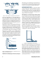
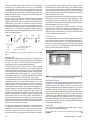
purely analog circuits. An ideal bandpass filter, with the frequency
Analog Dialogue 31-1 (1997)
As Figure 1 shows, an analog approach using second-order filters
would require quite a few staggered high-Q sections; the difficulty
of tuning and adjusting it can be imagined.
PASSBAND
IDEAL
RESPONSE
IDEAL
RESPONSE
|H(f)|
by David Skolnick and Noam Levine
Useful additions would include:
• passband tuning and width control
• stopband rolloff control.
ROLLOFF
ROLLOFF
2ND
ORDER
2ND
ORDER
STOPBAND
f0
STOPBAND
f
Figure 1. An ideal bandpass filter and second-order
approximations.
With DSP software, there are two basic approaches to filter design:
finite impulse response (FIR) and infinite impulse response (IIR).
The FIR filter’s time response to an impulse is the straightforward
weighted sum of the present and a finite number of previous input
samples. Having no feedback, its response to a given sample ends
when the sample reaches the “end of the line” (Figure 2). An FIR
filter’s frequency response has no poles, only zeros. The IIR filter,
by comparison, is called infinite because it is a recursive function:
its output is a weighted sum of inputs and outputs. Since it is
recursive, its response can continue indefinitely. An IIR filter
frequency response has both poles and zeros.
IN THIS ISSUE
Volume 31, Number 1,1997,24 Pages
Editor’s Notes, Authors . . . . . . . . . . . . . . . . . . . . . . . . . . . . . . . . . . . . 2
Digital signal processing 101—an introductory course in DSP system design: I . . 3
Selecting mixed-signal components for digital communications systems—III . . . . 7
Controller board system allows for easy evaluation of general-purpose converters . . 10
Build a smart analog process-instrument transmitter with
low-power converters & microcontroller . . . . . . . . . . . . . . . . . . . . . . 13
New-Product Briefs:
Amplifiers, Buffered Switches and Multiplexers . . . . . . . . . . . . . . . 16
A/D and D/A Converters, Volume Controls . . . . . . . . . . . . . . . . . . 17
Power Management, Supervisory Circuits . . . . . . . . . . . . . . . . . . . 18
Mixed bag: Communications, Video, DSP . . . . . . . . . . . . . . . . . . . 19
Ask The Applications Engineer—24: Resistance . . . . . . . . . . . . . . . . . 20
Worth Reading, More authors . . . . . . . . . . . . . . . . . . . . . . . . . . . . . . 23
3
z –1
INPUT
(n–1)
(n–N+2)
z –1
a(0)
a(1)
z –1
a(N–2)
(n–N+1)
a(N–1)
∑
FIR
STRUCTURE
OUTPUT
SAMPLING REAL-WORLD SIGNALS
N–1
y(n) =
∑a(k)
(n–k)
k=0
a(0)
x(n)
z –1
z
y(n)
a(1)
b(1)
IIR
FILTER
–1
a(2)
y(n) =
z –1
z –1
b(2)
N–1
M
k=0
k=1
∑a(k) x (n–k) + ∑b(k) y (n–k)
Figure 2. Filter equations and delay-line representation.
The xs are the input samples, ys are the output samples, as are
input sample weightings, and bs are output sample weightings. n
is the present sample time, and M and N are the number of samples
programmed (the filter’s order). Note that the arithmetic operations
indicated for both types are simply sums and products—in
potentially great number. In fact, multiply-and-add is the case for
many DSP algorithms that represent mathematical operations of
great sophistication and complexity.
Approximating an ideal filter consists of applying a transfer function
with appropriate coefficients and a high enough order, or number
of taps (considering the train of input samples as a tapped delay
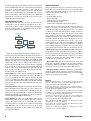
line). Figure 3 shows the response of a 90-tap FIR filter compared
with sharp-cutoff Chebyshev filters of various orders. The 90-tap
example suggests how close the filter can come to approximating
an ideal filter. Within a DSP system, programming a 90-tap FIR
filter—like the one in Figure 3—is not a difficult task. By
comparison, it would not be cost-effective to attempt this level of
approximation with a purely analog circuit. Another crucial point
in favor of using a DSP to approximate the ideal filter is long-term
stability. With an FIR (or an IIR having sufficient resolution to
avoid truncation-error buildup), the programmable DSP achieves
the same response, time after time. Purely analog filter responses
of high order are less stable with time.
0
90-TAP FIR
RELATIVE MAGNITUDE – dB
PASSBAND CUTOFF
FREQUENCY 0.5fS
–25
2
Real-world phenomena are analog—the continuously changing
energy levels of physical processes like sound, light, heat, electricity,
magnetism. A transducer converts these levels into manageable
electrical voltage and current signals, and an ADC samples and
converts these signals to digital for processing. The conversion
rate, or sampling frequency, of the ADC is critically important in
digital processing of real-world signals.
This sampling rate is determined by the amount of signal
information that is needed for processing the signals adequately
for a given application. In order for an ADC to provide enough
samples to accurately describe the real-world signal, the sampling
rate must be at least twice the highest-frequency component of
the analog signal. For example, to accurately describe an audio
signal containing frequencies up to 20 kHz, the ADC must sample
the signal at a minimum of 40 kHz. Since arriving signals can easily
contain component frequencies above 20 kHz (including noise),
they must be removed before sampling by feeding the signal
through a low-pass filter ahead of the ADC. This filter, known as
an anti-aliasing filter, is intended to remove the frequencies above
20 kHz that could corrupt the converted signal.
However, the anti-aliasing filter has a finite frequency rolloff, so
additional bandwidth must be provided for the filter’s transition
band. For example, with an input signal bandwidth of 20 kHz,
one might allow 2 to 4 kHz of extra bandwidth.
1/2 LSB
NOISE
20 24
FREQUENCY – kHz
–50
48
4
6
–75
–100
–125
0
f
0.1
0.2
0.3
0.4
0.5 fS
NORMALIZED FREQUENCY =
(ACTUAL FREQ) / (SAMPLING FREQ)
Figure 3. 90-tap FIR filter response compared with those of
sharp cutoff Chebyshev filters.
Mathematical transform theory and practice are the core
requirement for creating DSP applications and understanding their
4
limits. This article series walks through a few signal-analysis and processing examples to introduce DSP concepts. The series also
provides references to texts for further study and identifies software
tools that ease the development of signal-processing software.
Figure 4. Antialiasing filter ideal response.
Figure 4 depicts the filter needed to reject any signals with
frequencies above half of a 48-kHz sampling rate. Rejection means
attenuation to less than 1/2 least-significant bit (LSB) of the ADC’s
resolution. One way to achieve this level of rejection without a
highly sophisticated analog filter is to use an oversampling converter,
such as a sigma-delta ADC. It typically obtains low-resolution (e.g.,
1-bit) samples at megahertz rates—much faster than twice the
highest frequency component—greatly easing the requirement for
the analog filter ahead of the converter. An internal digital filter
(DSP at work!) restores the required resolution and frequency
response. For many applications, oversampling converters reduce
system design effort and cost.
Analog Dialogue 31-1 (1997)
PROCESSING REAL-WORLD SIGNALS
The ADC sampling rate depends on the bandwidth of the analog
signal being sampled. This sampling rate sets the pace at which
samples are available for processing. Once the system bandwidth
requirements have established the A/D converter sampling rate,
the designer can begin to explore the speed requirements of the
DSP processor.
Processing speed at a required sample rate is influenced by
algorithm complexity. As a rule, the DSP needs to finish all
operations relating to the first sample before receiving the second
sample. The time between samples is the time budget for the DSP
to perform all processing tasks. For the audio example, a 48-kHz
sampling rate corresponds to a 20.833-µs sampling interval. Figure
5 relates the analog signal and digital sampling rate.
ANALOG
t
t
LOWPASS FILTER
X(N)
H(Z)
Y(N)
ADC
DAC
Figure 6. Example of continuous processing of samples
in digital filter.
Frame-based systems, like a spectrum analyzer, which determines
the frequency components of a time-varying waveform, acquire a
frame (or block of samples). Processing occurs on the entire frame of
data and results in a frame of transformed data, as shown in Figure 7.
SIGNAL
ANALYSIS
DSP
SYSTEM
SAMPLING
INTERVAL
DIGITAL SAMPLE TIMES
Figure 5. Sampling train and processing time.
Next consider the relation between the speed of the DSP and
complexity of the algorithm (the software containing the transform
or other set of numeric operations). Complex algorithms require
more processing tasks. Because the time between samples is fixed,
the higher complexity calls for faster processing.
For example, suppose that the algorithm requires 50 processing
operations to be performed between samples. Using the previous
example’s 48-kHz sampling rate (20.833-µs sampling interval),
one can calculate the minimum required DSP processor speed, in
millions of operations per second (MOPS) as follows:
DSP Speed =
Operations
50
=
= 2.4 MOPS
Sampling Interval 20.833 µs
Thus if all of the time between samples is available for operations
to implement the algorithm, a processor with a performance level
of 2.4 MOPS is required. Note that the two common ratings for
DSPs, based on operations per second (MOPS) and instructions
per second (MIPS), are not the same. A processor with a 10-MIPS
rating that can perform 8 operations per instruction has basically
the same performance as a faster processor with a 40 MIPS rating
that can only perform 2 operations per instruction.
SAMPLING VARIOUS REAL-WORLD SIGNALS
There are two basic ways to acquire data, either one sample at a
time or one frame at a time (continuous processing vs. batch
processing). Sample-based systems, like a digital filter, acquire data
one sample at a time. As shown in Figure 6, at each tick of the
clock, a sample comes into the system and a processed sample is
output. The output waveform develops continuously.
Analog Dialogue 31-1 (1997)
TIME
FREQUENCY
Figure 7. Example of batch processing of a block of data.
For an audio sampling rate of 48 kHz, a processor working on a
frame of 1024 samples has a frame acquisition interval of 21.33 ms
(i.e., 1024 × 20.833 µs = 21.33 ms). Here the DSP has 21.33 ms
to complete all the required processing tasks for that frame of data.
If the system handles signals in real time, it must not lose any
data; so while the DSP is processing the first frame, it must also
be acquiring the second frame. Acquiring the data is one area where
special architectural features of DSPs come into play: Seamless
data acquisition is facilitated by a processor’s flexible dataaddressing capabilities in conjunction with its direct memoryaccessing (DMA) channels.
RESPONDING TO REAL-WORLD SIGNALS
One cannot assume that all the time between samples is available
for the execution of processing instructions. In reality, time must
be budgeted for the processor to respond to external devices,
controlling the flow of data in and out. Typically, an external device
(such as an ADC) signals the processor using an interrupt. The
DSP’s response time to that interrupt, or interrupt latency, directly
influences how much time remains for actual signal processing.
Interrupt latency (response delay) depends on several factors; the
most dominant is the DSP architecture’s instruction pipelining.
An instruction pipeline consists of the number of instruction cycles
that occur between the time an interrupt is received and the time
that program execution resumes. More pipeline levels in a DSP
result in longer interrupt latency. For example, if a processor has a
20-ns cycle time and requires 10 cycles to respond to an interrupt,
200 ns elapse before it executes any signal-processing instructions.
When data is acquired one sample at a time, this 200-ns overhead
will not hurt if the DSP finishes the processing of each sample
before the next arrives. When data is acquired sample-by-sample
while processing a frame at a time, however, an interrupted system
wastes processor instruction cycles. For example, a system with a
5
200-ns interrupt response time running a frame-based algorithm,
such as the FFT, with a frame size of 1024 samples, would require
204.8 µs of overhead. That amounts to more than 10,000
instruction cycles wasted to latency—productive time when the
DSP could be performing signal processing. This waste is easy to
avoid in DSPs having architectural features such as DMA and
dual memory access; they let the DSP receive and store data
without interrupting the processor.
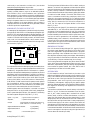
DEVELOPING A DSP SYSTEM
Having discussed the role of the processor, the ADC, the antialiasing filter, and the timing relationships between these
components, it is time to look at a complete DSP system. Figure 8
shows the building blocks of a typical DSP system that could be
used for data acquisition and control.
ANALOG INPUT
ANTI-ALIASING
FILTER
ADC
DSP
DAC
HOST
INTERFACE
ANTI-IMAGING
FILTER
DIGITAL I/O
ANALOG OUTPUT
Figure 8. Putting together elements of a DSP system.
Note how few components make up the DSP system, because so
much of the system’s functionality comes from the programmable
DSP. Converters funnel data into and out of the DSP; the ADC
timing is controlled by a precise sampling clock.To simplify system
design, many converter devices available today combine some or
all of the following: an A/D converter, a D/A converter, a sampling
clock, and filters for anti-aliasing and anti-imaging. The clock
oscillator in these types of I/O components is separately controlled
by an external crystal. Here are some important points about the
data flow in this sort of DSP system:
Analog Input: The analog signal is appropriately band-limited
by the anti-aliasing filter and applied to the input of the ADC. At
the selected sampling time, the converter interrupts the DSP
processor and makes the digital sample available. The choice
between serial and parallel interfacing between the ADC and DSP
depends on the amount of data, design complexity trade-offs, space,
power, and price.
Digital Signal Processing: The incoming data is handled by the
DSP’s algorithm software. When the processor completes the
required calculations, it sends the result to the DAC. Because the
signal processing is programmable, considerable flexibility is
available in handling the data and improving system performance
with incremental programming adjustments.
Analog Output: The DAC converts the DSP’s output into the
desired analog output at the next sample clock. The converter’s
output is smoothed by a low-pass, anti-imaging filter (also called a
reconstruction filter), to produce the reconstructed analog signal.
Host Interface: An optional host interface lets the DSP
communicate with external systems, sending and receiving data
and control information.
6
REVIEW AND PREVIEW
The goal of this article has been to provide an overview of major
DSP design concepts and explain some of the reasons why a DSP
is better suited that analog circuitry for some applications. The
issues introduced in this article include:
• DSP overview
• Real-time DSP operation
• Real-world signals
• Sampling rates and anti-alias filtering
• DSP algorithm time budget
• Sample driven versus frame driven data acquisition
Because these issues involve many valuable levels of detail that we
could not do justice to in this brief article, you should consider
reading Richard Higgins’s text, Digital Signal Processing in VLSI
(see References below). This text provides a complete overview of
DSP theory, implementation issues, and reduction to practice (with
devices available at the time it was published), plus exercises and
examples. The Reference section below also contains other sources
that further amplify this article’s issues. To prepare for the next
articles in this series, you might want to get free copies of the
ADSP-2100 Family User’s Manual* and the ADSP-2106x SHARC
User’s Manual.* These texts provide information on Analog
Devices’s fixed- and floating-point DSP architectures, a major topic
in these articles. The next article will cover the following territory:
• Mathematical overview of signal processing: It will present
the mathematics for the transform functions (frequency domain)
and convolution functions (time domain) that appear throughout
the series. While the mathematical treatment is necessarily
incomplete (no derivations), there will be sufficient detail for
considering how to program the operations.
• DSP architecture: The article will discuss the nature and
functioning of the DSP’s arithmetic-logic unit (ALU), multiplyaccumulator (MAC), barrel-shifter, and memory busses—and
describe the numeric operations that support DSP functions.
• DSP programming concepts: A discussion of programming
will bring together theory and practice (math and architecture).
Finally, it will lay out the main parameters for a series-length DSP
design project, provided as an example.
b
References
Higgins, R. J. Digital Signal Processing inVLSI, Englewood Cliffs, NJ: Prentice
Hall, 1990. DSP basics. Includes a wide-ranging bibliography. Available for
purchase from ADI. See the book purchase card.
Mar, A., ed. Digital Signal Processing Applications Using the ADSP-2100 Family—
Volume 1, Englewood Cliffs, NJ: Prentice Hall, 1992. Available for purchase
from ADI. See the book purchase card.
Mar, A., Babst, J., eds. Digital Signal Processing Applications Using the ADSP2100 Family—Volume 2, Englewood Cliffs, NJ: Prentice Hall, 1994. Available
for purchase from ADI. See the book purchase card.
Dearborn, G., ed. Digital Signal Processing Applications Using the ADSP-21000
Family—Volume 1, Norwood, MA: Analog Devices, Inc., 1994. Available for
purchase from ADI.0 See the book purchase card.
*Mar, A., Rempel, H., eds. ADSP-2100 Family User’s Manual, Norwood, MA:
Analog Devices, Inc., 1995. Free. Circle 1
Mar, A., Rempel, H., eds. ADSP-21020 Family User’s Manual, Norwood, MA:
Analog Devices, Inc., 1995. Free. Circle 2
*Rempel, H., ed. ADSP-21060/62 SHARC User’s Manual, Norwood, MA:
Analog Devices, Inc., 1995. Free. Circle 3
Analog Dialogue 31-1 (1997)
Why use a DSP?
(handling instructions and data, testing status, etc.) to implement
the formula in software.
[Digital Signal Processing 101—
An Introductory Course in DSP
System Design—Part 2]
by David Skolnick and Noam Levine
If you’ve read Part 1 of this series (or are already familiar with
some of the ways a DSP can work with real-world signals), you
might want to learn more about how digital filters (such as those
described in Part 1) can be implemented with a DSP. This article,
the second of a series, introduces the following DSP topics:
• Modeling filter transform functions
• Relating the models to DSP architecture
• Experimenting with digital filters
This series seeks to describe these topics from the perspective of
analog system designers who want to add DSP to their design
repertoire. Using the information from articles in this series as an
introduction, designers can make more informed decisions about
when DSP designs might be more productive than analog circuits.
Modeling Filter Transform Functions
Part 1 compared analog and digital filter properties and suggested
why one might implement these filters digitally (using DSP); this
part focuses on some of the mechanics of digital filter application.
The three principal reasons for using digital filtering are (1) closer
approach to ideal filter approximations, (2) ability to adjust filter
characteristics in software rather than by physical tuning, and (3)
compatibility of filter response with sampled data. The two bestknown filters described in Part 1 are the finite impulse-response
(FIR) and infinite impulse-response (IIR) types. The FIR filter
response is called finite because its output is based solely on a
finite set of input samples; it is non-recursive and has no poles,
only zeroes in its s-plane. The IIR filter, on the other hand, has a
response that can go on indefinitely (and can be unstable) because
it is recursive, i.e., its output values are affected by both input and
output. It has both poles and zeroes in its s-plane. Figure 1 shows
the typical filter architectures and summation formulas that
appeared in Part 1.
z–1
INPUT
x(n–1)
a(0)
z–1
x(n–N+2)
a(1)
z–1
a(N–2)
FIR
STRUCTURE
x(n–N+1)
a(N–1)
OUTPUT
N–1
y(n) =
a(k)x(n–k)
k=0
a(0)
x(n)
z–1
z–1
y(n)
a(1)
b(1)
IIR
FILTER
a(2)
y(n) =
b(2)
z–1
z–1
M
N–1
a(k)x(n–k) +
b(k)y(n–k)
k=0
k=1
Figure 1. Filter equations and their delay-line models.
To model these filters digitally, one might take two steps. First,
view these formulas as programs running on a computer. This
step consists of breaking down the formula into the mathematical
steps (e.g., multiply and add) and identifying all of the additional
operations that would be necessary for a computer to perform
Analog Dialogue 31-2 (1997)
Second, take those operations and write them as a program. This
can be a fairly arduous task. Fortunately, there is much “canned”
software available, often in a high-level language (HLL) such as
C, somewhat simplifying (but by no means eliminating!) the job
of programming. From the point of view of learning, though, it
may be more instructive to start with assembly language; also
assembly language algorithms are often more useful than HLL
where system performance must be optimized. At the level of
abstraction of some high-level languages, the program may not
look much like the equations. For example, Figure 2 shows an
example of an FIR algorithm implemented as a C program.*
float fir_filter(float input, float *coef, int n, float *history)
{
int i;
float *hist_ptr, *hist1_ptr, *coef_ptr;
float output;
hist_ptr = history;
hist1_ptr = hist_ptr;
/* use for history update */
coef_ptr = coef + n -1;
/* point to last coef */
/*form output accumulation */
output = *hist_ptr++ * (*coef_ptr-);
for(i = 2; i < n; i++)
{
*hist1_ptr++ = *hist_ptr; /* update history array */
output += (*hist_ptr++) * (*coef_ptr-);
}
output += input * (*coef_ptr); /* input tap */
*hist1_ptr = input;
/* last history */
return(output);
}
Figure 2. FIR Filter as C program.
There are many analysis packages available that support algorithm
modeling; see the references at the end of this article for several
popular packages. We will return to algorithm modeling at various
times in the course of this series. Now, continuing the discussion
of the process, after these filter algorithms have been modeled,
they are ready for implementation in DSP architecture.
Relating The Models To DSP Architecture: For programming,
one must understand four sections of DSP architecture: numeric,
memory, sequencer, and I/O operations. This architectural
discussion is generic (applying to general DSP concepts), but it is
also specific as it relates to programming examples later in this
article. Figure 3 shows the generalized DSP architecture that this
section describes.
ARCHITECTURE
Numeric Section: Because DSPs must complete multiply/
accumulate, add, subtract, and/or bit-shift operations in a single
instruction cycle, hardware optimized for numeric operations is
central to all DSP processors. It is this hardware that distinguishes
DSPs from general-purpose microprocessors, which can require
many cycles to complete these types of operations. In the digital
filters (and other DSP algorithms), the DSP must complete
multiple steps of arithmetic operations involving data values and
coefficients, to produce responses in real time that have not been
possible with general-purpose processors.
Numeric operations occur within a DSP’s multiply/accumulator
(MAC), arithmetic-logic unit (ALU), and barrel shifter (shifter).
The MAC performs sum-of-products operations, which appear in
most DSP algorithms (such as FIR and IIR filters and fast Fourier
transforms). ALU capabilities include addition, subtraction, and
*From Embree, P. M., C algorithms for real-time DSP. Upper Saddle River, NJ:
Prentice Hall (1995).
11
logical operations. Operations on bits and words occur within the
shifter. Figure 3 shows the parallelism of the MAC, ALU, and
shifter and how data can flow into and out of them.
ADDRESS GENERATOR #1
ADDRESS GENERATOR #2
PROGRAM SEQUENCER
L0 - L3
I0 - I3
MODULUS
LOGIC
M0 - M3
ADDER
L4 - L7
I4 - I7
MODULUS
LOGIC
COUNTER
LOGIC
M4 - M7
LOOP
LOGIC
STATUS
LOGIC
ADDER
PROGRAM MEMORY ADDRESS BUS
DATA MEMORY ADDRESS BUS
PROGRAM MEMORY DATA BUS
DATA MEMORY DATA BUS
ALU
MAC
AX0
AY0
MX0
MY0
AX1
AY1
MX1
MY1
ALU
AF
MAC
SHIFTER
BLOCK
FLOATING
POINT
LOGIC
SR1 SR0
MR2 MR1 MR0
RESULT BUS
Figure 3. A useful DSP architecture.
From a programming point of view, a DSP architecture that uses
separate numeric sections provides great flexibility and efficiency.
There are many non-conflicting paths for data, allowing singlecycle completion of numeric operations. The architecture of the
DSP must also provide a wide dynamic range for MAC operations,
with the ability to handle multiplication results that are double
the width of the inputs—and accumulator outputs that can mount
up without overflowing. (On a 16-bit DSP, this feature equates to
16-bit data inputs and a 40-bit result output from the MAC.) One
needs this range for handling most DSP algorithms (such as filters).
Other features of the numeric section can facilitate programming
in real-time systems. By making operations contingent on a variety
of conditional states, which result from numeric operations, these
can serve as variables in a program’s execution, testing for carries,
overflows, saturates, flags, or other states. Using these conditionals,
a DSP can rapidly handle decisions about program flow based on
numeric operations. The need to be constantly feeding data into
the numeric section is a key design influence on the DSP’s memory
and internal bus structures.
Memory Section: DSP memory and bus architecture design is
guided by the need for speed. Data and instructions must flow
into the numeric and sequencing sections of the DSP on every
instruction cycle. There can be no delays, no bottlenecks.
Everything about the design focuses on throughput.
To put this focus on throughput in perspective, one can look at
the difference between DSP memory design and memory for other
microprocessors. Most microprocessors use a single memory space
containing both data and instructions, using one bus for address
and other for data or instructions. This architecture is called von
Neumann architecture. The limitation on throughput in a von
Neumann architecture comes from having to choose between either
a piece of data or an instruction on each cycle. In DSPs, memory
is typically divided into program and data memory—with separate
busses for each. This type of architecture is referred to as Harvard
architecture. By separating the data and instructions, the DSP can
fetch multiple items on each cycle, doubling throughput. Additional
optimizations, such as instruction cache, results feedback, and
context switching also increase DSP throughput.
12
“Howard Aiken, developer of the Harvard series of machines,
insisted on the separation of data and programs in all his
machines. In the Mark III, which I know best, he even had
different size drums for each.”
“The von Neumann concept was that by treating instructions
as data one could make alterations in programs, enhancing
the ability for programs to ‘learn’.”
“For some reason, the latter was given von Neumann’s name,
while the former took its name from the Harvard line of
machines.”
SHIFTER
MF
EXPONENT
LOGIC
AR
SI
Etymology of Harvard and von Neumann Architectures—
According to John A. N. Lee, Department of Computer Science,
Virginia Tech:
Other optimizations in DSP memory architecture relate to repeated
memory accesses. Most DSP algorithms, such as digital filters,
need to get data from memory in a repeating pattern of accesses.
Typically, this type of access serves to fetch data from a range of
addresses, a range that is filled with data from the real-world signals
to be processed. By reducing the number of instructions needed
to “manage” memory accesses (overhead), DSPs “save” instruction
cycles, allowing more time for the main job of each cycle—
processing signals. To reduce overhead and automatically manage
these types of accesses, DSPs utilize specialized data addressgenerators (DAGs).
Most DSP algorithms require two operands to be fetched from
memory in a single cycle to become inputs to the arithmetic units.
To supply the addresses of these two operands in a flexible manner,
the DSP has two DAGs. In the DSP’s modified Harvard
architecture, one address generator supplies an address over the
data-memory address bus; the other supplies an address over the
program-memory address bus. By performing these two data
fetches in time for the next numeric instruction, the DSP is able
to sustain single-cycle execution of instructions.
DSP algorithms, such as the example digital filters, usually require
data in a range of addresses (a buffer) to be addressed so that the
address pointer “wraps-around” from the end of the buffer back
to the start of the buffer (buffer length). This pointer movement is
called circular buffering. (In the filter equations, each summation
basically results from a sequence of multiply-and-accumulates of
a circular buffer of data points and a circular buffer of coefficients).
A variation of circular buffering, which is required in some
applications, advances the address pointer by values greater than
one address per “step,” but still wraps around at a given length
This variation is called modulo circular buffering.
By supporting various types of buffering with its DAGs, the DSP
is able to perform address modify and compare operations in
hardware for optimum efficiency. Performing these functions in
software (as occurs in general purpose processors) limits the
processor’s ability to handle real-time signals.
Because buffering is an unusual concept, yet key to digital signal
processing, a brief buffering example is useful. In the example
illustrated in Figure 4, a buffer of eight locations resides in memory
starting at address 30. The address generator must calculate next
addresses that stay within this buffer yet keep the proper data
spacing so that two locations are skipped. The address generator
outputs the address 30 on to the address bus while it modifies the
Analog Dialogue 31-2 (1997)
address to 33 for the next cycle’s memory access. This process
repeats, moving the address pointer through the buffer. A special
case occurs when the address 36 gets modified to 39. The address
39 is outside the buffer. The address generator detects that the
address has fallen outside of the buffer boundary and modifies
the address to 31 as if the end of the buffer is connected to the
start of the buffer. The update, compare, and modify occur with no
overhead. In one cycle, the address 36 is output onto the address
bus. On the next cycle, the address 31 is output onto the address
bus. This modulo circular buffering serves the needs of algorithms
such as interpolation filters and saves instruction cycles for
processing.
ADDRESS SEQUENCE
Input/Output (I/O) Section: As noted again and again, there is
a need for tremendous throughput of data to the DSP; everything
about its design is focused on funneling data into and out of the
numeric, memory, and sequencer sections. The source of the data—
and destination of the output (the result of signal processing)—is
the DSP’s connection to its system and the real-world. A number
of I/O functions are required to complete signal processing tasks.
Off-DSP memory arrays store processor instructions and data.
Communication channels (such as serial ports, I/O ports and direct
memory accessing (DMA) channels transfer data into and out of
the DSP quickly. Other functions (such as timers and program
boot logic) ease DSP system development. A brief list of typical
I/O tasks in a DSP system includes the following (among many
others):
• Boot loading: At Reset, the DSP loads instructions form an
external source (EPROM or host) usually through an external
memory interface.
0x0030
30
31
32
33
• Serial communications: The DSP receives or transmits data
through a synchronous serial port (SPORT), communicating
with codecs, ADCs, DACs, or other devices.
34
35
0x0037
36
37
• Memory-mapped I/O: The DSP receives or transmits data
through an off-DSP memory location that is decoded by an
external device.
Figure 4. Example of modulo circular buffering.
Sequencer Section: Because most DSP algorithms (such as the
example filters) are by nature repetitive, the DSP’s program
sequencer needs to loop through the repeated code without
incurring overhead while getting from the end of the loop back to
the start of the loop. This capability is called zero-overhead looping.
Having the ability to loop without overhead is a key area in which
DSPs differ from conventional microprocessors. Typically,
microprocessors require that program loops be maintained in
software, placing a conditional instruction at the end of the loop.
This conditional instruction determines whether the address
pointer moves (jumps) back to the top of the loop or to another
address. Because getting these addresses from memory takes time—
and availability of time for signal-processing is critical in DSP
applications—DSPs cannot waste cycles retrieving addresses for
conditional program sequencing (branching) in this manner.
Instead, DSPs perform these test and branch functions in hardware,
storing the needed addresses.
As Figure 5 shows, the DSP executes the last instruction of the
loop in one cycle. On the next cycle, the DSP evaluates the
conditional and executes either the first instruction at the top of
the loop or the first instruction outside the loop. Because the DSP
uses dedicated hardware for these operations, no extra time is
wasted with software evaluating conditionals, retrieving addresses,
or branching program execution.
GENERAL FORM:
DO LABEL UNTIL CONDITION
EXAMPLE:
ADDRESS SAVED
BY HARDWARE
ENDLOOP:
CNTR=10;
DO ENDLOOP UNTIL CE;
{
{
{
{
FIRST LOOP INSTRUCTION }
;
NEXT LOOP INSTRUCTION }
;
LAST LOOP INSTRUCTION }
;
FIRST INSTRUCTION OUTSIDE LOOP }
ADDRESS SAVED
BY HARDWARE
;
EXPERIMENTING WITH DIGITAL FILTERS
Having modeled the filter algorithms and looked at some of the
DSP architectural features, one is ready to start looking at how
these filters could be coded in DSP assembly language. Up to this
point the discussion and examples have been generic, applying to
almost all DSPs. Here, the example is specific to the Analog Devices
ADSP-2181. This processor is a fixed-point, 16-bit DSP. The term
“fixed-point” means that the “point” separating the mantissa and
exponent does not change its bit location during arithmetic
operations. Fixed-point DSPs can be more challenging to program,
but they tend to be less expensive than floating-point DSPs. The
“16-bit” in “16-bit DSP” refers to the size of the DSP’s data words.
This DSP uses 16-bit data words and 24-bit wide instruction words.
DSPs are specified by the size of the data, rather than instruction
width because data word size describes the width of data that the
DSP can handle most efficiently.
The example program in Figure 6 is an FIR filter in ADSP-2181
assembly language. The software has two parts. The main routine
includes register and buffer initialization along with the interrupt
vector table, and the interrupt routine that executes when a data
sample is ready. After initialization, the DSP executes instructions
in the main routine, performing some background tasks, looping
through code, or idling in a low-power standby mode until it gets
an interrupt from the A/D converter. In this example, the processor
idles in a low-power standby mode waiting for an interrupt.
The FIR filter interrupt subroutine (the last segment of code) is
the heart of the filter program. The processor responds to the
interrupt, saving the context of the main routine and jumping to
the interrupt routine. This interrupt routine processes the filter
input sample, reading data and filter coefficients from memory
and storing them in data registers of the DSP processor. After
processing the input sample, the DSP sends an output sample to
the D/A converter.
Figure 5. Example of program loop.
Analog Dialogue 31-2 (1997)
13
.module/RAM/ABS=0
FIR_PROGRAM;
/******** Initialize Constants and Variables *****************/
.const
taps=127;
.var/dm/circ
data[taps];
.var/pm/circ
fir_coefs[taps];
.init
fir_coefs: <coeffs.dat>;
.var/dm/circ
output_data[taps];
/******** Interrupt vector table *****************************/
reset_svc: jump start; rti; rti; rti;
/*00: reset */
irq2_svc:
/*04: IRQ2 */
si=io(0);
/* get next sample */
dm(i0,m0)=si;
/* store in tap delay line */
jump fir;
/* jump to fir filter */
nop;
/* nop is placeholder */
irql1_svc: rti; rti; rti; rti; /*08: IRQL1 */
irql0_svc: rti; rti; rti; rti; /*0c: IRQL0 */
sp0tx_svc: rti; rti; rti; rti; /*10: SPORT0 tx */
sp0rx_svc: rti; rti; rti; rti; /*14: SPORT1 rx */
irqe_svc:
rti; rti; rti; rti; /*18: IRQE */
bdma_svc:
rti; rti; rti; rti; /*1c: BDMA */
sp1tx_svc: rti; rti; rti; rti; /*20: SPORT1 tx or IRQ1 */
sp1rx_svc: rti; rti; rti; rti; /*24: SPORT1 rx or IRQ0 */
timer_svc: rti; rti; rti; rti; /*28: timer */
pwdn_svc:
rti; rti; rti; rti; /*2c: power down */
/******* START OF PROGRAM — initialize mask, pointers **********/
start:
/* set up various control registers */
ICNTL=0x07;
/* set IRQ2, IRQ1, IRQ0 edge sensitive */
IFC=0xFF;
/* clear all pending interrupts */
NOP;
/* add nop because of one cycle */
/* synchronization delay of IFC */
SI=0x0000;
DM(0x3FFF)=SI;
/* sports not enabled */
/* sport1 set for IRQ1, IRQ0, FI, FO */
IMASK=0x200;
/* enable IRQ2 interrupt */
i0=^data;
/* index to data buffer */
l0=taps;
/* length of data buffer */
m0=1;
/* post modify value */
i4=^fir_coefs;
/* index to fir_coefs buffer */
l4=taps;
/* length of fir_coefs buffer */
m4=1;
/* post modify value */
i2=^output_data; /* index to data buffer */
l2=taps;
/* length of data buffer */
cntr=taps;
do zero until ce;
dm(i0,m0)=0; /* clear out the tap delay data buffer */
zero:
dm(i2,m0)=0; /* clear out the output_data buffer */
/**** WAIT for IRQ2 Interrupt — then JUMP to INTERRUPT VECTOR **/
wait:
idle;
/* wait for IRQ2 interrupt */
jump wait;
/******* FIR FILTER interrupt subroutine ***********************/
fir
cntr=taps-1;
/* set up loop counter */
mr=0, mx0=dm(i0,m0), my0=pm(i4,m4);
/* fetch data and coefficient */
do fir1loop until ce; /* set up loop */
fir1loop: mr=mr+mx0*my0(ss), mx0=dm(i0,m0), my0=pm(i4,m4);
/* calculations */
/* if not ce jump fir1loop;*/
mr=mr+mx0*my0(rnd); /* round final result to 16-bits */
if mv sat mr;
/* if overflow, saturate */
io(1)=mr1;
/* send result to DAC */
dm(i2,m0)=mr1;
rti;
/******* END OF PROGRAM *************************************/
.endmod;
Figure 6. An FIR filter in ADSP-2181 assembly language.
Note that this program uses DSP features that perform operations
with zero overhead, usually introduced by a conditional. In
particular, program loops and data buffers are maintained with
zero overhead. The multifunction instruction in the core of the
filter loop performs a multiply/accumulate operation while the next
data word and filter coefficient are fetched from memory.
The program checks the final result of the filter calculation for
any overflow. If the final value has overflowed, the value is saturated
to emulate the clipping of an analog signal. Finally, the context of
the main routine is restored and the instruction flow is returned
to the main routine with a return from interrupt (RTI) instruction.
14
REVIEW AND PREVIEW
The goal of this article has been to provide a link between filter
theory and digital filter implementation. On the way, this article
covers modeling filters with HLL programs, using DSP
architecture, and experimenting with filter software. The issues
introduced in this article include:
• Filters as programs
• DSP architecture (generalized)
• DSP assembly language
Because these issues involve many valuable levels of detail that
one could not do justice to in this brief article, you should consider
reading Richard Higgins’s text, Digital Signal Processing in VLSI,
and Paul Embree’s text, C Algorithms For Real Time DSP (see
References below). These texts provides a complete overview of
DSP theory, implementation issues, and reduction to practice (with
devices available at the time of publication), plus exercises and
examples. The Reference section below also contains other sources
that further amplify this article’s issues. To prepare for the next
articles in this series, you might want to get free copies of the
ADSP-2100 Family User’s Manual* or the ADSP-2106x SHARC
User’s Manual.* These texts provide information on Analog
Devices’s fixed- and floating-point DSP architectures, a major topic
in these articles. Working through this series, each part adds some
feature or information contributing to the series goal of developing
a DSP system. To reach this goal, the next article describes the
series’ development platform (the ADSP-2181 EZ-KIT LITE)
and introduces additional DSP development topics.
References
• Dearborn, G., ed., Digital Signal Processing Applications Using
the ADSP-21000 Family—Volume 1, Norwood, MA: Analog
Devices, Inc., 1994. Available from ADI. See the book
purchase card.
• Embree, P. M., C Algorithms for Real-Time DSP. Upper Saddle
River, NJ: Prentice Hall (1995). Not available from ADI.
• Higgins, R. J., Digital Signal Processing in VLSI, Englewood Cliffs,
NJ: Prentice Hall, 1990. DSP basics. Includes a wide-ranging
bibliography. Available from ADI. See the book purchase card.
• Mar, A., ed., Digital Signal Processing Applications Using the ADSP2100 Family—Volume 1, Englewood Cliffs, NJ: Prentice Hall,
1992. Available from ADI. See the book purchase card.
• Mar, A., Babst, J., eds., Digital Signal Processing Applications Using
the ADSP-2100 Family—Volume 2, Englewood Cliffs, NJ: Prentice
Hall, 1994. Available from ADI. See the book purchase card.
• Mar, A., Rempel, H., eds., ADSP-2100 Family User’s Manual,
Norwood, MA: Analog Devices, Inc., 1995. Free. Circle 5
• Mar, A., Rempel, H., eds., ADSP-21020 Family User’s Manual,
Norwood, MA: Analog Devices, Inc., 1995. Free. Circle 6
• MATLAB For DSP Design (an analysis and design package for
DSP), contact The Math Works, Inc. at: phone (508) 647-7000,
fax: (508) 647-7101, or Web site: http://www.mathworks.com
• QEDesign (digital filter design software), contact Momentum
Data Systems at: phone (714) 557-6884, fax: (714) 557-6969,
or Web site: http://www.mds.com
• Rempel, H., ed., ADSP-21060/62 SHARC User’s Manual,
b
Norwood, MA: Analog Devices, Inc., 1995. Free.
Analog Dialogue 31-2 (1997)
DSP 101 Part 3:
Implement Algorithms
on a Hardware
Platform
by Noam Levine and David Skolnick
So far, we have described the physical architecture of the DSP
processor, explained how DSP can provide some advantages over
traditionally analog circuitry, and examined digital filtering,
showing how the programmable nature of DSP lends itself to such
algorithms. Now we look at the process of implementing a finiteimpulse-response (FIR) filter algorithm (briefly introduced in Part
2, implemented in ADSP-2100 Family assembly code) on a
hardware platfor m, the ADSP-2181 EZ-Kit Lite™. The
implementation is expanded to handle data I/O issues.
the beginning of the program, and the circular buffering mechanism
ensures that the pointer does not leave the bounds of its assigned
memory buffer—a capability used extensively in the FIR filter code
for both input delay line and coefficients. Once the elements of
the program have been determined, the next step is to develop the
DSP source code to implement the algorithm.
DEVELOPING DSP SOFTWARE
Software development flow for the ADSP-2100 Family consists
of the following steps: architecture description, source-code
generation, software validation (debugging), and hardware
implementation. Figure 2 shows a typical development cycle.
GENERATE
ARCHITECTURE
DESCRIPTION
(.SYS)
ARCHITECTURE DESCRIPTION
SYSTEM BUILDER
BLD21
GENERATE
ASSEMBLY
SOURCE
(.DSP)
ASSEMBLER
ASM21
USING DIGITAL FILTERS
Many of the architectural features of the DSP, such as the ability
to perform zero-overhead loops, and to fetch two data values in a
single processor cycle, will be useful in implementing this filter.
Reviewing briefly, an FIR filter is an all-zeros filter that is calculated
by convolving an input data-point series with filter coefficients. Its
governing equation and direct-form representation are shown in
Figure 1.
x(n)
INPUT
h(0)
z–1
x(n–1)
z–1
h(1)
x(n–N+2)
z–1
x(n–N+1)
h(N–2)
OUTPUT
GENERATE C
SOURCE
(.C)
C COMPILER
G21
SYSTEM
VERIFICATION
HARDWARE EVALUATION
EZ-KIT LITE
EZ-LAB
SIMULATOR
SIM21xx
SOFTWARE VERIFICATION
TARGET VERIFICATION
EZ-ICE
NO
YES
WORKING
CODE?
ROM PRODUCTION
SPL21
Figure 2. Software development flow.
h(N–1)
N–1
y(n) =
h(m)x(n–m)
m=0
Figure 1. Direct-form FIR filter structure.
In this structure, each “z–1” box represents a single increment of
history of the input data in z-transform notation. Each of the
successively delayed samples is multiplied by the appropriate
coefficient value, h(m), and the results, added together, generate a
single value representing the output corresponding to the nth input
sample. The number of delay elements, or filter taps, and their
coefficient values, determine the filter’s performance.
The filter structure suggests the physical elements needed to
implement this algorithm by computation using a DSP. For the
computation itself, each output sample requires a number of
multiply-accumulate operations equal to the length of the filter.
The delay line for input data and the coefficient value list require
reserved areas of memory in the DSP for storing data values and
coefficients. The DSP’s enhanced Harvard architecture lets
programmers store data in Program Memory as well as in Data
Memory, and thus perform two simultaneous memory accesses in
every cycle from the DSP’s internal SRAM. With Data Memory
holding the incoming samples, and Program Memory storing the
coefficient values, both a data value and a coefficient value can be
fetched in a single cycle for computation.
This DSP architecture favors programs that use circular buffering
(discussed briefly in Part 2 and later in this installment). The
implication is that address pointers need to be initialized only at
12
CODE GENERATION
LINKER
LD21
AND/OR
Architecture description: First, the user creates a software
description of the hardware system on which the algorithm runs.
The system description file includes all available memory in the
system and any memory-mapped external peripherals. Below is
an example of this process using the ADSP-2181 EZ-Kit Lite.
Source-code generation: Moving from theory into practice, this
step—where an algorithmic idea is turned into code that runs on
the DSP—is often the most time-consuming step in the process.
There are several ways to generate source code. Some programmers
prefer to code their algorithms in a high-level language such as C;
others prefer to use the processor’s native assembly language.
Implementations in C may be faster for the programmer to develop,
but compiled DSP code lacks efficiency by not taking full advantage
of a processor’s architecture.
Assembly code, by taking full advantage of a processor’s design,
yields highly efficient implementations. But the programmer needs
to become familiar with the processor’s native assembly language.
Most effective is combining C for high-level program-control
functions and assembly code for the time-critical, math-intensive
portions of the system. In any case, the programmer must be aware
of the processor’s system constraints and peripheral specifics. The
FIR filter system example in this article uses the native assembly
language of the ADSP-2100 Family.
Software validation (“debugging”): This phase tests the results
of code generation—using a software tool known as a simulator—
to check the logical flow of the program and verify that an algorithm
is performing as intended. The simulator is a model of the DSP
processor that a) provides visibility into all memory locations and
processor registers, b) allows the user to run the DSP code either
Analog Dialogue 31-3 (1997)
continuously or one instruction at a time, and c) can simulate
external devices feeding data to the processor.
Hardware implementation: Here the code is run on a real DSP,
typically in several phases: a) tryout on an evaluation platform
such as EZ-Kit Lite; b) in-circuit emulation, and c) production
ROM generation. Tryout provides a quick go/no-go determination
of the program’s operation; this technique is the implementation
method used in this article. In-circuit emulation monitors software
debug in the system, where a tool such as an EZ-ICE™ controls
processor operation on the target platform. After all debug is
complete, a boot ROM of the final code can be generated; it serves
as the final production implementation.
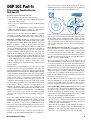
WORKING WITH THE ADSP-2181 EZ-KIT LITE
Our example of the development cycle walks through the process,
using the ADSP-2181 EZ-Kit Lite (development package ADDS21xx-EZLITE) as the target hardware for the filter algorithm. The
EZ-Kit Lite, a low-cost demonstration and development platform,
consists of a 33-MHz ADSP-2181 processor, an AD1847 stereo
audio codec, and a socketed EPROM, which contains monitor
code for downloading new algorithms to the DSP through an RS232 connection (Figure 3).
RS-232
9VDC
a
ADSP-2181
STEREO
OUT
STEREO
IN
a
AD1847
CODEC
EPROM
LINE/MIC
JUMPER
RESET IRQE
FL1
Figure 3. Layout of EZ-Kit Lite board.
To complete the architecture description phase, one needs to know
the memory and memory-mapped peripherals that the DSP has
available to it. Programmers store this information in a systemdescription file so that the development tools software can produce
appropriate code for the target system. The EZ-Kit Lite needs no
memory external to the DSP, because available memory on-chip
consists of the 16,384 locations of the ADSP-2181’s Program
Memory (PM) SRAM, and 16,352 locations of Data Memory
(DM) SRAM. (32 DM locations used for system control registers
are not available for working code). More information on the
ADSP-2181, the EZ-Kit Lite’s architecture, and related topics,
can be found in texts mentioned at the end of this article.
Available system resources information is recorded in a system
description file for use by the ADSP-2100 Family development
tools. A system description file has a .SYS extension.The following
list shows a system description file [EZKIT_LT.SYS]:
.system
EZ_LITE;
.adsp2181;
.mmap0;
/* gives a name to this system */
/* specifies the processor
*/
/* specifies that the system boots and that */,
/* PM location 0 is in internal memory
*/
.seg/PM/RAM/ABS=0/code/data
int_pm[16384];
.seg/DM/RAM/ABS=0
int_dm[16352];
.endsys;
/* ends the description */
Analog Dialogue 31-3 (1997)
After writing the code (page 15), the next step is to generate an
executable file, i.e., turn the code into instructions that the DSP
can execute. First one assembles the DSP code. This converts the
program file into a format that the other development tools can
process. Assembling also checks the code for syntax errors. Next,
one links the code to generate the DSP executable, using the
available memory that is declared in the architecture file. The
Linker fits all of the code and data from the source code into the
memory space; the output is a DSP executable file, which can be
downloaded to the EZ-Kit Lite board.
GENERATING FILTER CODE
PWR
EZ-PORT
The listing declares 16,384 locations of PM as RAM, starting at
address 0, to let both code segments and data values be placed
there. Also declared are 16,352 available locations of data memory
as RAM, starting at address 0. Because these processors use a
Harvard architecture with two distinct memory spaces, PM address
0 is distinct from DM address 0. The ADSP-2181 EZ-Kit Lite’s
codec is connected to the DSP using a serial port, which is not
declared in the system description file. To make the system
description file available to other software tools, the System Builder
utility, BLD21, converts the .SYS file into an architecture, or
.ACH, file. The output of the System Builder is a file named
EZKIT_LT.ACH.
Part 2 of this series [Analog Dialogue 31-2, page 14, Figure 6]
introduced a small assembly code listing for an FIR filter. Here,
that code is augmented to incorporate some EZ-Kit Lite-specific
features, specifically codec initialization and data I/O. The core
filter-algorithm elements (multiply-accumulates, data addressing
using circular buffers for both data and coefficients, and reliance
on the efficiency of the zero-overhead loop) do not change.
The incoming data will be sampled using the on-board AD1847
codec, which has programmable sampling rate, input gain, output
attenuation, input selection, and input mixing. Its programmable
nature makes the system flexible, but it also adds a task of
programming to initialize it for the DSP system.
ACCESSING DATA
For this example, a series of control words to the codec—to be
defined at the beginning of the program in the first section of the
listing—will initialize it for an 8-kHz sampling rate, with moderate
gain values on each of the input channels. Since the AD1847 is
programmable, users would typically reuse interface and
initialization code segments, changing only the specific register
values for different applications. This example will add the specific
filter segment to an existing code segment found in the EZ-Kit
Lite software.
This interface code declares two areas in memory to be used for
data I/O: “tx_buf”, for data to be transmitted out of the codec,
and “rx_buf ”, where incoming data is received. Each of these
memory areas, or buffers, contains three elements, a control or
status word, left-channel data, and right-channel data. For each
sample period, the DSP will receive from the codec a status word,
left channel data, and right channel data. On every sample period,
the DSP must supply to the codec a transmit control word, left
channel data, and right channel data. In this application, the control
information sent to the codec will not be altered, so the first word
in the transmit data buffer will be left as is. We will assume that the
source is a monophonic microphone, using the right channel (no
concern about left-channel input data).
13
Using the I/O shell program found in the EZ-Kit Lite software,
we need only be involved with the section of code labeled
“input_samples”. This section of code is accessed when new data
is received from the codec ready to be processed. If only the right
channel data is required, we need to read the data located in data
memory at location rx_buf + 2, and place it in a data register to be
fed into the filter program.
The data arriving from the codec needs to be fed into the filter
algorithm via the input delay line, using the circular buffering
capability of the ADSP-2181. The length of the input delay line is
determined by the number of coefficients used for the filter.
Because the data buffer is circular, the oldest data value in the
buffer will be wherever the pointer is pointing after the last filter
access (Figure 4) . Likewise the coefficients, always accessed in
the same order every time through the filter, are placed in a circular
buffer in Program Memory.
MEMORY
LOCATION
READ
WRITE
READ
0
X(4)
X(8)
X(8)
1
X(5)
X(5)
2
X(6)
X(6)
X(6)
3
X(7)
X(7)
X(7)
WRITE
READ
X(9)
X(9)
X(8)
4-TAP EXAMPLES
Y(7)=
h(0)x(7)+h(1)x(6)+h(2)x(5)+h(3)x(4)
Y(8)=
Y(9)=
h(0)x(8)+h(1)x(7)+h(2)x(6)+h(3)x(5)
can be performed in parallel with two data accesses, one from
Data Memory, one from Program Memory. This capability means
that on every loop iteration a MAC operation is being performed.
At the same time, the next data value and coefficient are being
fetched, and the counter is automatically decremented. All without
wasting time maintaining loops.
As the filter code is executed for each input data sample, the output
of the MAC loop will be written to the output data buffer, tx_buf.
Although this program only deals with single-channel input data,
the result will be written out to both channels by writing to memory
buffer addresses tx_buf+1 and tx_buf+2.
The final source code listing is shown on page 15. The filter
algorithm itself is listed under “Interrupt service routines”. The
rest of the code is used for codec and DSP initialization and
interrupt service routine definition. Those topics will be explored
in future installments of this series.
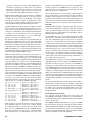
THE EZ-KIT LITE
The Windows-based monitor software provided with the EZ-Kit
Lite, makes it possible to load an executable file into the ADSP2181 on the EZ-Kit Lite board. This is accomplished through the
pull-down “Loading” menu by selecting “Download user program
and Go” (Figure 5). This will download the filter program to the
ADSP-2181 and start program execution.
h(0)x(9)+h(1)x(8)+h(2)x(7)+h(3)x(6)
Figure 4. Example of using circular buffers for filter data
input.
Algorithm Code
To operate on the received data, the code section published in the
last installment can be used with few modifications. To implement
this filter, we need to use the multiply/accumulate (MAC)
computational unit and the data address-generators.
The ADSP-2181’s MAC stores the result in a 40-bit register
(32 bits for the product of 2 16-bit words, and 8 bits to allow the
sum to expand without overflowing). This allows intermediate filter
values to grow and shrink as necessary without corrupting data.
The code segment being used is generic (i.e., can be used for any
length filters); so the MAC’s extra output bits allow arbitrary filters
with unknown data to be run with little fear of losing data.
Figure 5. EZ-Kit Lite download menu.
To implement the FIR filter, the multiply/accumulate operation is
repeated for all taps of the filter on each data point. To do this
(and be ready for the next data point), the MAC instruction is
written in the form of a loop. The ADSP-21xx’s zero-overhead
loop capability allows the MAC instruction to be repeated for a
specified number of counts without programming intervention. A
counter is set to the number of taps minus one, and the loop
mechanism automatically decrements the counter for each loop
operation. Setting the loop counter to “taps–1” ensures that the
data pointers end up in the correct location after execution is
finished and allows the final MAC operation to include rounding.
As the AD1847 is a 16-bit codec, the MAC with rounding provides
a statistically unbiased result rounded to the nearest 16-bit value.
This final result is written to the codec.
REVIEW AND PREVIEW
For optimal code execution, every instruction cycle should perform
a meaningful mathematical calculation. The ADSP-21xxs
accomplish this with multi-function instructions: the processor
can perform several functions in the same instruction cycle. For
the FIR filter code, each multiply-accumulate (MAC) operation
REFERENCES
14
The goal of this article was to outline the steps from an algorithm
description to a DSP executable program that could be run on a
hardware development platform. Issues introduced include
software development flow, architecture description, source-code
generation, data I/O, and the EZ-Kit Lite hardware platform
There are many levels of detail associated with each of these topics
that this brief article could not do justice to. Further information
is available in the references below. The series will continue to
build on this application with additional topics. The next article
will examine data input/output (I/O) issues in greater detail through
the processor interrupt structure, and discuss additional features
of the simple filter algorithm.
ADSP-2100 Family Assembler Tools & Simulator Manual. Consult
your local Analog Devices Sales Office.
ADSP-2100 Family User’s Manual. Analog Devices. Free.
Circle 4
b
Analog Dialogue 31-3 (1997)
FIR Filter code listing for EZ-Kit Lite
/**************************************************************
*
* hello81.dsp — template file for 2181 ez-kit lite board
*
* This sample program is organized into the following sections:
*
* Assemble time constants (system.h)
* Interrupt vector table
* ADSP 2181 intialization (init1847.dsp)
* ADSP 1847 codec intialization (init1847.dsp)
* Interrupt service routines
*
* This program implements a simple ‘talk-through’ with the AD1847 codec.
* The initialization routines have been put into the init1847.dsp file. This
* file contains the interrupt vector table, the main ‘dummy’ loop, and the
* interrupt service routines for the pushbutton and the serial port 0 receive.
* The pushbutton (IRQE) causes the LED on the EZ-Kit board to toggle
* with each button press.
*
* Parameters controlling the sampling rate, gains, etc., are contained in the
* file init1847.dsp. Serial Port 0 is used to communicate with the AD1847.
* The transmit interrupts are used to configure the codec, then they are
* disabled and the receive interrupts are used to implement the ‘talk-through’
* audio.
*
* The definitions for the memory-mapped control registers are contained in
* the file: system.h
*
* The application can be built by:
*
* asm21 -c -l -2181 hello81
* asm21 -c -l -2181 init1847
* ld21 hello81 init1847 -a 2181 -e hello81 -g -x
*
**************************************************************/
.module/RAM/ABS=0 EzHello;
#include <system.h>
#define taps 255
/* filter tap length */
.var/dm/circ
filt_data[taps];
/* input data buffer */
.var/pm/circ
filt_coeffs[taps];
/* coefficient buffer */
.init filt_coeffs:<coefs.dat>;
/* initialize coefficients */
.external rx_buf, tx_buf;
.external init_cmds, stat_flag;
.external next_cmd, init_1847, init_system_regs, init_sport0;
/**************************************************************
* Interrupt vector table
**************************************************************/
jump start; rti; rti; rti;
/* 00: reset */
rti; rti; rti; rti;
/* 04: IRQ2 */
rti; rti; rti; rti;
/* 08: IRQL1 */
rti; rti; rti; rti;
/* 0c: IRQL0 */
ar = dm(stat_flag);
/* 10: SPORT0 tx */
ar = pass ar;
if eq rti;
jump next_cmd;
jump input_samples;
/* 14: SPORT1 rx */
rti; rti; rti;
jump irqe; rti; rti; rti;
/* 18: IRQE */
rti; rti; rti; rti;
/* 1c: BDMA */
rti; rti; rti; rti;
/* 20: SPORT1 tx or IRQ1 */
rti; rti; rti; rti;
/* 24: SPORT1 rx or IRQ0 */
rti; rti; rti; rti;
/* 28: timer */
rti; rti; rti; rti;
/* 2c: power down */
/**************************************************************
* ADSP 2181 intialization
**************************************************************/
Analog Dialogue 31-3 (1997)
start:
i0 = ^rx_buf;
/* remember codec autobuffering uses i0 and i1 !! */
l0 = %rx_buf;
i1 = ^tx_buf;
l1 = %tx_buf;
i3 = ^init_cmds;
/* i3 can be used for something else after codec init */
l3 = %init_cmds;
m0 = 0;
m1 = 1;
/* initialize serial port 0 for communication with the AD1847 codec */
call init_sport0;
/* initialize the other system registers, etc. */
call init_system_regs;
/* initialize the AD1847 codec */
call init_1847;
ifc = b#00000011111111;
/* clear any pending interrupt */
nop;
/* there is a 1 cycle latency for ifc */
/* setup pointers for data and coefficients */
i2 = ^filt_data;
l2 = %filt_data;
i5 = ^filt_coefs;
m5 = 1;
l5 = %filt_coefs;
imask=b#0000110000; /* enable rx0 interrupt */
/* |||||||||+ | timer
||||||||+- | SPORT1 rec or IRQ0
|||||||+-- | SPORT1 trx or IRQ1
||||||+--- | BDMA
|||||+---- | IRQE
||||+----- | SPORT0 rec
|||+------| SPORT0 trx
||+-------| IRQL0
|+--------| IRQL1
+---------| IRQ2
*/
/*--------------------------------------------------------------------------- wait for interrupt and loop forever
---------------------------------------------------------------------------*/
talkthru: idle;
jump talkthru;
/**************************************************************
* Interrupt service routines
**************************************************************/
/*--------------------------------------------------------------------------- FIR Filter
---------------------------------------------------------------------------*/
input_samples:
ena sec_reg;
/* use shadow register bank */
ax0 = dm (rx_buf + 1);
/* read data from converter */
dm(i2,m1) = ax0;
/* write new data into delay line, pointer
now pointing to oldest data */
cntr = taps - 1;
mr = 0, mx0 = dm(i2,m1), my0 = pm(i5,m5); /* clear accumulator, get first
data and coefficient value */
do filt_loop until ce;
/* set-up zero-overhead loop */
filt_loop: mr = mr + mx0 * my0(ss), mx0 = dm(i2,m1), my0 = pm(i5,m5);
/* MAC and two data fetches */
mr = mr + mx0 * my0 (rnd); /* final multiply, round to 16-bit result */
if mv saat mr;
/* check for overflow */
dm(tx_buf+1) = mr1;
dm(tx_buf+2) = mr1;
/* output data to both channels */
rti;
.endmod;
15
DSP 101 Part 4:
Programming Considerations for
Real-time I/O
DSP system software design. Time management strategy
determines how the processor gets notified about events, influences
data handling, and shapes processor communications.
12
9
by Noam Levine and David Skolnick
12:38 107. 5
3
6
So far, this series has introduced the following topics:
• Part 1 (vol. 31-1): DSP architecture and DSP advantages over
traditionally analog circuitry
• Part 2 (vol. 31-2): digital filtering concepts and DSP filtering
algorithms
• Part 3 (vol. 31-3): implementation of a finite-impulse- response
(FIR) filter algorithm and an overview of a demonstration
hardware platform, the ADSP-2181 EZ-Kit Lite™.
Extra
m
p
Sa
Transf
er
Pr
oc
es
s
Co
n
g
in
pl
ro
ce
ss
g
in
pl
ol
ntr
Co
Extra
Sa
m
Analog Dialogue 32-1 (1998)
Transf
er
Pr
oc
es
s
Since there is a finite amount of time that can be budgeted to
perform any given algorithm, managing time is a central part of
l
ro
nt
Co
Digital
Extra
Signal
Tra
ProcessingP nsfer
Sa
m
In the filter example described earlier in this series, the input
sampling rate is 8␣ kHz. For the DSP in the example to keep up
with real-time data, all processing has to be done within a time
budget of 1/(8␣ kHz), or 125␣ µs. On a 33-MHz digital signalprocessor (30␣ ns per cycle), the time budget provides 125␣ µs/30␣ ns,
or 4166 instruction cycles, to complete processing and any other
required tasks.
Analog
Signal
Processing
g
lin
ol
ntr
Co
Extra
This definition of real time implies that, for a processor operating
at a given clock rate, the speed and quantity of the input data
determines how much processing can be applied to the data without
falling behind the data stream.The idea of having a limited amount
of time with which to handle data may seem odd to analog designers
because this concept does not have a parallel in analog systems. In
analog systems, signals are processed continuously. The only
penalty in a slow system is limited frequency response. By
comparison, digital systems process parts of the signal, enough
for very accurate approximations, but only within a limited block
of time. Figure 1 shows a comparison. Real-time DSP can be
limited by the amount of data or type of processing that can be
completed within the algorithm’s time budget. For example, a given
DSP processor handling data values sampled at, say, 48-kHz (audio
signals), has less time to process those data values, including
execution of all necessary tasks, than one sampling 8-kHz voiceband data.
Time
Tr ansf
er
Pr
oc
es
s
What does “real-time” mean? In an analog system, every task
is performed in “real time” with continuous signals and processing.
In a digital signal-processing (DSP) system, signals are represented
with sets of samples, i.e., values at discrete points in time. Thus
the time for processing a given number of samples in a DSP system
can have an arbitrary interpretation in “real time”, depending on
the sampling rate. The first article in this series introduces the
concept of sampling and the Nyquist criterion—that in real-time
applications, the sampling frequency must be at least twice the
frequency of the highest frequency component of interest in the
(analog) signal (Nyquist rate). The time between samples is referred
to as the sampling interval. To consider a system as operating in
“real time,” all processing of a given set of data (one or more
samples, depending on the algorithm) must be completed before
new data arrives.
R
uous espo
tin
e
ns
Now, we look more closely at DSP programming concerns that
are unique to real-time systems. This article focuses on how to
develop algorithms for DSP systems with a variety of I/O interfaces.
Time
tinuous Dat
Con
a
Figure 1. Comparison of analog and digital signal processing.
a.␣ Analog:␣ A response value corresponds to each data value
at all instants of time. b.␣ Digital:␣ For each sample, the data
must be transferred in and processed, an event marks the
end of processing (control), and extra time may be necessary for other tasks within the cycle after the designated process occurs.
Event Notification: Interrupts: One can program a DSP to
process data using one of several strategies for handling the “event,”
the arrival of data. A status bit or flag pin could be read periodically
to determine whether new data is available. But—“polling” wastes
processor cycles. The data may arrive just after the last poll, but it
can’t make its presence known until the next poll. This makes it
difficult to develop real-time systems.
The second strategy is for the data to interrupt the processor on
arrival. Using interrupts to notify the processor is efficient, though
not as easy to program; clock cycles can be wasted during the wait
for an interrupt. Nevertheless, event-driven interrupt programming
being well-suited to processing real-world signals promptly, most
DSPs are designed to deal efficiently with them. In fact, they are
designed to respond very quickly to interrupts. The ADSP-2181’s
response time to an interrupt is about three processor cycles; i.e.,
within 75␣ ns the DSP has stopped doing what it was doing and is
handling the interrupt event (vector).
In many DSP-based systems, the interrupt rates, based on the
input data sampling rate, are often totally unrelated to the DSP’s
clock rate. In the FIR example seen earlier in this series, the
processor is interrupted at 125-µs intervals to receive new data.
Interrupt Handling and Interrupt Vectors: Because interrupt
processing is such a vital element in DSP systems, processors
typically have built-in hardware mechanisms to handle interrupts
efficiently. Hard-wired mechanisms are more efficacious than
software alone because a DSP’s interrupt service routines (ISRs)
may have to meet all of the following demands:
•
•
Fast context switching—switch from working on one task and
its data (a context) to another context without the time loss and
complication associated with writing programs to save register
contents and chip status information.
Nested-interrupt handling—handle multiple interrupts of
different priorities “simultaneously.” The DSP handles one
interrupt at a time, but an interrupt of higher priority can take
precedence over the handling of a lower-priority interrupt.
9
• Continue to accept data/record status—while the DSP services
an interrupt, events keep on occurring in the real world and
data keeps on arriving. To keep up with the “real-world,” the
DSP must record these events and accept the data—then
process them when it has finished servicing the interrupt.
On Analog Devices DSPs, fast context switching is accomplished
using two sets of data registers. Only one set is active at a time,
containing all the data in process during that context. When
servicing an interrupt, the computer can switch from the active
to the alternate set without having to temporarily save the data
in memory. This facilitates rapid switching between tasks.
To handle multiple interrupts, Analog Devices DSPs record their
state for each one. Processor state information is kept on a set of
status “stacks” located in the DSP’s Program Sequencer. A “stack”
consists of a set of hardware registers. Current status information
is “pushed” onto the stack when an event occurs. This stack
mechanism also allows interrupts to be nested; one with higher
priority can interrupt one with lower priority.
Two hardware features, interrupt latch and automated I/O, let
Analog Devices DSPs stay abreast of the “real world” while
processing an interrupt. The latch keeps the DSP from missing
important events while servicing an interrupt. The other feature,
comprising various forms of automated I/O (including serial ports,
DMA, autobuffering, etc.) lets external devices pump data into
the DSP’s memory without requiring intervention from the DSP.
So no data is missed while the DSP is “busy.”
When an interrupt request is generated, by an external source or
an internal resource, the DSP processor automatically stores its
current state of operation, and prepares to execute the interrupt
routine. Interrupt routines are dispatched from an interrupt vector
table. An interrupt vector table is an area in Program Memory
with instruction addresses assigned to particular DSP interrupt
functions. For example, in the table below, a Transmit (Tx)
interrupt at serial port 1 (SPORT1) of an ADSP-2181 processor
will cause the next instruction to be executed at program memory
(PM) location 0x0020, followed by the contents of the next three
locations, through 0x0023 (the interrupt routine). As the 12 items
in the table indicate, an ADSP-2181 can handle interrupts from
11 locations (external hardware, DMA ports, and the serial ports)
and the processor Reset. The table lists the programmed
instructions assigned to each interrupt vector source in memory
locations 0x0000 to 0x002F for an FIR filter program.
Jump
rti;
rti;
rti;
ar =
jump
start; nop; nop; nop; /*
nop; nop; nop;
/*
nop; nop; nop;
/*
nop; nop; nop;
/*
dm(stat_flag); ar = pass
/*
input_samples; nop; nop;
/*
irqe; nop; nop; nop; /*
nop; nop; nop;
/*
nop; nop; nop;
/*
nop; nop; nop;
/*
nop; nop; nop;
/*
PM(0x0000-03):
PM(0x0004-07):
PM(0x0008-0B):
PM(0x000C-0F):
ar; if eq_rti;
PM(0x0010-13):
nop;
PM(0x0014-17):
PM(0x0018-1B):
PM(0x001C-1F):
PM(0x0020-23):
PM(0x0024-27):
PM(0x0028-2B):
Reset vector */
IRQ2 vector */
IRQL1 vector */
IRQL0 vector */
jump next_cmd;
SPORT0 Tx vector */
SPORT0 Rx vector */
IRQE vector */
BDMA vector */
SPORT1 Tx vector */
SPORT1 Rx vector */
Timer vector */
within the four available instruction locations, they are programmed
directly, as shown in the SPORT0 Tx vector (0x0010-13). Any
unused interrupt vectors call for return from interrupt (rti), with
three nop (no operation) instructions.
The nop instructions serve as place holders—instruction space
used to ensure that the correct interrupt action lines up with the
hardware-specified interrupt vector. The rti instruction at the
beginning of each unused vector location is both placeholder and
safety valve. If an unused interrupt is mistakenly unmasked or
inadvertently triggered, “rti” causes a return to normal execution.
Data I/O
In DSP systems, interrupts are typically generated by the arrival
of data or the requirement to provide new output data. Interrupts
may occur with each sample, or they may occur after a frame of
data has been collected. The differences greatly influence how the
DSP algorithm deals with data.
For algorithms that operate on a sample-by-sample basis, DSP
software may be required to handle each incoming and outgoing
data value. Each DSP serial port incorporates two data I/O
registers, a receive register (Rx), and a transmit register (Tx). When
a serial word is received, the port will typically generate a Receive
interrupt. The processor stops what it is doing, begins executing
code at the interrupt vector location, reads the incoming value
from the Rx register into a processor data register, and either
operates on that data value or returns to its background task. In
the table above, the computer jumps to a program segment,
“input_samples”, performs whatever instructions are programmed
in that segment, and returns from the interrupt, either directly or
via a return to the interrupt vector.
To transmit data, the serial port can generate a Transmit interrupt,
indicating that new data can be written to the SPORT Tx register.
The DSP can then begin code execution at the SPORT Tx
interrupt vector and typically transfer a value from a data register
to the SPORT Tx register. If data input and output are controlled
by the same sampling clock, only one interrupt is necessary. For
example, if a program segment is initiated by Receive interrupt
timing, new data would be read during the interrupt routine; then
either the previously computed result, which is being held in a
register, would be transmitted, or a new result would be computed
and immediately transmitted—as the final step of the interrupt
routine.
All of these mechanisms help a DSP to approach the ability to
emulate what an analog system does naturally—continuously
process data in real time—but with digital precision and flexibility.
In addition, in an efficiently programmed digital system, spare
processor cycles left between processing data sets can be used to
handle other tasks.
/* PM(0x002C-2F): Powerdown vector */
Programming Considerations
In a “real-time” system, processing speed is of the essence. By
using SPORT autobuffering, no time is lost to data I/O. Instead,
the data management goal is to make sure that the selected address
points to the new data.
Each interrupt vector has four instruction locations. Typically,
these instructions will cause the processor to jump to another
area of memory in order to process the data, as is shown in the
Reset (at 0x0000), SPORT0 Rx (0x0014), and IRQE (0x0018)
interrupt vectors. If there are just a few steps—such as reading a
value, checking status, or loading memory—that can be done
In the FIR filter example (Analog Dialogue 31-3, page 15), a SPORT
Receive interrupt request is generated when the input autobuffer
is full, meaning that the DSP has received three data words: status,
left channel data, and right channel data. Since this simplified
application uses single-channel data, only the data value that resides
at location rx_buf+1 is used by the algorithm.
jump
rti;
rti;
rti;
rti;
rti; nop; nop; nop;
10
Analog Dialogue 32-1 (1998)
Filter Algorithm Expansion In other applications, the data handling
can be more involved. For example, if the FIR filter of the example
were expanded to a two-channel implementation, the core DSP
algorithm code would not have to change. The code relating to
data handling, however, would have to be modified to account for
a second data stream and a second set of coefficients.
In the filter code, two new buffers in memory would be required
to handle both the additional data stream and the additional set of
coefficients. The core filter loop may be isolated as a separate
“callable” function. This technique lets the same code be used,
regardless of the input data values. Benefits of this programming
style include readable code, re-usable algorithms, and reduced code
size. If a modular approach is not taken, the filter loop would have
to be repeated, using additional DSP memory space.
The SPORT Receive interrupt routine would then consist of the
setting of pointer and calling the filter. The revised filter routine is
shown in the following listing:
Filter: cntr = taps - 1;
mr = 0, mx0 = dm(i2,m1), my0 = pm(i5,m5);
/* clear accumulator, get first data
and coefficient value */
do filt_loop until ce;
/* set-up zero-overhead loop */
filt_loop: mr = mr + mx0*my0(ss), mx0 = dm(i2,m1),
my0 = pm(i5,m5);
/* MAC and two data fetches */
mr = mr + mx0 * my0 (rnd); /* final multiply, round to 16-bit
result */
if mv sat mr;
/* check for overflow*/
rts;
/* return */
It’s important to note that the only modifications to the core filter
loop were the addition of a label, “Filter:” at the beginning of the
routine, and the addition of an “rts” (return from subroutine)
instruction at the end. These additions change filter code from a
stand-alone routine into a subroutine that can be called from other
routines. No longer a single-purpose routine, it has become a reusable, callable subroutine.
With the core filter set up as a callable subroutine, the two-channel
data handling requirements can now be addressed. To simplify
some of the programming issues, this example assumes that both
the left and right channels use the same filter coefficients.
In the third installment of this series, the entire filter application
assembly code was displayed. At the top of the code listing, all of
the required memory buffers were declared. To expand the filter
application to handle two channels of data, the required new
variables and buffers need to be declared. For the incoming data,
the buffer declaration,
.var/dm/circ_filt_data[taps]; /* input data buffer */
These locations in memory are going to be used to store address
values appropriate for each data stream. The circular buffering
capability of the ADSP-2181 is used to ensure that the data pointer
is always in the correct place in the buffer whenever the filter is
executed. Because the subroutine is now dealing with two buffers,
the pointer locations need to be saved when processing for each
channel is completed.
To set up the pointers, two variables in data memory need to be
declared as follows:
.var/dm filter1_ptr;
.var/dm filter2_ptr;
/* data pointer for left channel data */
/* data pointer for right channel data */
These variable then need to be initialized with the starting address
of each of the data buffers;
.init filter1_ptr: ^filt1_data; /* initialize starting point,
left channel */
.init filter2_ptr: ^filt2_data; /* initialize starting point,
right channel */
The DSP assembler software recognizes the symbol “^” to mean
“address of.” The DSP linker software fills in the appropriate
address value. In this way, the pointer variables in the executable
program are initialized with the starting addresses of the
appropriate memory buffers.
The following listing shows how the FIR Filter interrupt routine
uses these new memory elements. The original Filter subroutine
from the 3rd installment has been modified to provide two separate
channels of filtering. Instead of launching directly into the filter
calculation, the routine must first load the appropriate data pointer.
The filter routine is then called, and the resulting output is placed
in the correct location for transmission.
/* ---------------------input_samples:
ena sec_reg;
FIR Filter ----------------------- */
/* use shadow register bank */
/* set up for filter 1 */
i2 = dm(filter1_ptr);
/* set data pointer for filter 1 */
ax0 = dm(rx_buf + 1);
/* read left channel data */
dm(i2,m1) = ax0;
/* write new data into delay line,
pointer now pointing to oldest data */
call filter;
/* perform the first filter for left
channel data */
dm(tx_buf+1) = mr1;
dm(filter1_ptr) = i2;
/* write left-channel output data */
/* save updated filter1 data pointer */
/* set up for filter 2 */
i2 = dm(filter2_ptr);
/* set data pointer for filter 2 */
ax0 = dm(rx_buf + 2);
/* read right channel data */
dm(i2,m1) = ax0;
/* write new data into delay line,
pointer now pointing to oldest data */
would need to be replaced with two buffers, declared as
call filter;
/* perform the filter again for the
right channel data */
Because both channels are to have the same filter coefficients
applied to them, the data buffers are of equal length.
dm(tx_buf+2) = mr1;
dm(filter2_ptr) = i2;
/* write right channel output data */
/* save updated filter2 data pointer */
The filter loop subroutine expects certain data and coefficient
values to be accessed using particular address registers. Specifically,
address register I2 must point to the oldest data sample, and I5
must point to the proper coefficient value prior to the filter routine
being called.
rti;
/* return from interrupt */
.var/dm/circ_filt1_data[taps]; /* left channel input data buffer */
.var/dm/circ_filt2_data[taps]; /* right channel input data buffer */
Because the filters for both the left and right channel will be sharing
the same memory pointers, there has to be a mechanism for
differentiating the two data streams. For the data pointer, I2, two
new variables need to be defined, “filter1_ptr” and “filter2_ptr.”
Analog Dialogue 32-1 (1998)
Because the core filter algorithm no longer handles data I/O, this
subroutine can be expanded to more channels of filtering by merely
adding more pointer variables and declaring more buffer space
(as long as sufficient memory exists!) Similarly, different
coefficients can be used for the two filters by setting up variables
that contain coefficient-buffer pointer information. In either case,
the filter algorithm does not need to be altered. By using this style
of modular programming, the user can build up a library of callable
11
DSP functions. Differences for particular systems can thus be
reduced to data-handling issues rather than the development of
new algorithms. While this programming style does not necessarily
allow the algorithm to perform its task more quickly, the system
designer has more flexibility in establishing how data flows through
the system.
Real-Time Interface Issues: So far, we have examined how
real-time programming in embedded systems relies on rapid
interrupt response, efficient data handling, and fast program
execution. In addition, the flow of data into and out of the
processor also influences how well the system will work in a realtime embedded environment.
The primary data flows into and out of a digital signal processor
can be both parallel and serial. Parallel transfers are typically at
least as wide as the native data word of the processor’s architecture
(16 bits for an ADSP-2100 Family processor, 32 bits for the
SHARC®). Parallel transfers occur via the external memory bus
or external host interface bus of the processor. Serial data transfers
require considerably fewer interconnections; they are frequently
used to communicate with data converters.
Serial Interface: Ease of hardware interfacing is an important
element of efficient DSP system implementation.The ADSP-2181
EZ-Kit Lite system uses an AD1847 serial codec (COder/
DECoder). Serial codecs permit data transfers via a serial port
(SPORT) on the DSP. This serial port is not an RS-232 PC-style
asynchronous serial port; it is a 5-wire synchronous interface that
passes bit-clock, Receive-data, Transmit-data, and framesynchronization signals. Major benefits of serial interfaces are
low pin count and ease of hardware hookup. The AD1847 requires
only 4 signals to interface to the DSP: serial clock, Receive data,
Transmit data, and Receive frame-synchronization signal. The
serial data stream is time-division multiplexed (TDM), meaning
that the same physical line can carry more than one type of
information in serial order. In the case of the AD1847 application
on EZ-Kit Lite, initiated in the last issue, the serial line carries
both left- and right-channel audio information, along with codec
control and status information. As noted earlier, the processor
has various means for handling this data. SPORT Interrupts are
generated automatically by the serial port hardware for either
Receive or Transmit data and for either a single word or a block
of words (Figure 2).
FO
/RESET
SDI
DT0
SDO
DR0
SDFS
RFS0
SCLK
+5V
Interrupt handling is different for the serial and parallel interfaces.
Since the external data bus of the DSP processor is a generalpurpose entity handling all sorts of data, it does not have dedicated
signal lines for interrupt generation and control; however, other
DSP resources are available. On the ADSP-2181, several external
hardware interrupt lines, such as the one for I/O memory select,
are available for triggering by an external device, such as an A/D
converter or codec. Such an interface is shown in Figure 3, involving
a parallel device and the ADSP-2181 DSP.
A0–A13
14
DMS OR
PMS
ADDRESS
DECODE
LOGIC
RD
WR
D8–D23
ADSP–21xx
CS
OE
RD
16
D0–D15
PARALLEL DEVICE
Figure 3. Parallel I/O inter facing for a DSP.
When responding to the interrupt for parallel data, the processor
reads the appropriate source and typically places that data value
in memory, by executing instructions similar to those shown here:
irq2_svc: ax0 = IO(ad_converter); dm(i2,m1) = ax0; rti;
“ad_converter” is a previously defined address in I/O space.
REVIEW AND PREVIEW
The goal of this article has been to detail the programming
concerns that DSP developers face when handling I/O and other
events in real-time systems. Issues introduced include real-time
data (samples and frames), interrupts and interrupt-handling,
automated I/O, and generalizing routines to make callable
subroutines. This brief article could not do justice to the many
levels of detail associated with each of these topics. Further
information is available in the references below. Future topics in
this series will continue to build on this application.The next article
will add more features to our growing example program and
describe software validation (i.e., debugging) techniques.
REFERENCES
ADSP-218x
16-BIT DSP
Figure 2. Serial inter facing between digital signal processor
and I/O device.
Parallel Interface: Even with a serial bit clock running as fast as
the DSP processor, a serial interface trades data transfer speed
for simplicity of wiring, transferring a data word at a fraction of
12
Parallel data transfer is always faster than serial transfers. The DSP
can perform an external access every processor cycle, but this
requires really fast parallel peripherals that can keep up with it,
such as fast SRAM chips. Parallel data transfers with other entities
usually occur at less than one per processor cycle.
SCLK
BM
AD1847
SOUNDPORT
STEREO CODEC
the DSP processor speed. For system performance that requires
higher data rates, a parallel interface can be used.When interfacing
in parallel, the DSP exercises its external data and address busses
to read or write data to a peripheral device. On the ADSP-2181,
the buses can interface with up to 16 bits of data.
ADSP-2100 Family Assembler Tools & Simulator Manual. Consult
your local Analog Devices Sales Office.
ADSP-2100 Family User’s Manual. Analog Devices. Free.
b
Many valuable publications can be found in the Design Support
area of our Web site under Product Documentation. A useful
bookmark is:
http://www.analog.com/support/product_documentation/dsp_prdoc.html
Analog Dialogue 32-1 (1998)