1
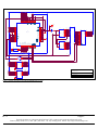
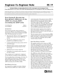
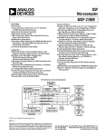
Engineer-To-Engineer's Note
EE-79
Technical Notes on using Analog Devices’ DSP components and development tools
Phone: (800) ANALOG-D, FAX: (781) 461-3010, EMAIL: [email protected], FTP: ftp.analog.com, WEB: www.analog.com/dsp
Copyright 1999, Analog Devices, Inc. All rights reserved. Analog Devices assumes no responsibility for customer product design or the use or application of customers’ products or
for any infringements of patents or rights of others which may result from Analog Devices assistance. All trademarks and logos are property of their respective holders. Information
furnished by Analog Devices Applications and Development Tools Engineers is believed to be accurate and reliable, however no responsibility is assumed by Analog Devices
regarding the technical accuracy of the content provided in all Analog Devices’ Engineer-to-Engineer Notes.
EPROM Booting In Host Mode
With 100 Pin 218x Processors
Written By:
Last Modified:
Greg F.
9/23/98
This EE Note will explain how to boot an Analog
Device’s adsp218x DSP processor (2184/85/86/87/89) via
the Byte Memory interface (BDMA) while it is
configured for host memory mode. Host memory mode
allows a host processor to boot or access the DSP’s
internal memory via the Internal Direct Memory
Addressing port (IDMA). Normally, these processors can
be configured to boot in only one of two methods; from
an eprom (full memory mode), or from a host processor
via the IDMA port (host memory mode).
sheet, available on our website at the following URL;
http://www.analog.com
Full Memory Mode
Full Memory Mode gives complete use of the external
address and data busses as found in the ADSP-2181. In
Full Memory Mode, the ADSP-2185/2186 behaves like
an ADSP-2181 with the IDMA port removed. There is a
24 bit external data bus, a 14 bit address bus and 5
memory select signals. Byte memory is accessed using
the middle eight bits of the data bus for data. The upper
eight bits of the data bus together with the 14 address pins
provide a 22 bit address for byte memory space. All of
these features behave exactly the same as on the ADSP2181. Hold Off cases (autobuffer cycle stealing, external
memory accesses with wait states, etc.) are simplified
because an IDMA transfer will never occur. In this mode
the IDMA port is disabled as if /IS was deselected or
pulled high on the ADSP-2181.
Overview
All of the previously mentioned processors feature a 100pin package which uses a multiplexed external bus that
has the following functionality:
•
Full Memory Mode : Provides complete use of the
external address and data busses as found in the
ADSP-2181. Allows BDMA operation with full
external overlay memory and I/O capability. IDMA
functionality is disabled
•
Host Mode: Allows complete IDMA port operation
with limited external addressing capabilities.
The functionality of the external bus is dependent upon
the setting of the external mode C pin of the processor.
The logic state of this pin is acknowledged by the
processor during reset; mode C = 0 configures the DSP in
full memory mode, mode C = 1 configures the processor
in host memory mode.
Note: the state of the mode C pin must not be changed
once the DSP begins execution. For more information on
the operation and configurations of the Mode C pin,
please refer to the appropriate ADSP-2185/6/7L data
Host Mode
Host Mode gives full use of the IDMA port as found on
the ADSP-2181, but there are limitations on the use of the
external memory bus. In Host Mode the lower eight bits
of the data bus, D[7:0] become IDMA control pins and
IAD bus pins. The upper 13 bits of the address bus
A[13:1] become the lower 13 bits of the IDMA
address/data bus, IAD[12:0]. The Pinout Diagram and
tables for the Memory Interface Pins in the ADSP2185/6/7L Data Sheets show the alternate functions for
each pin in either major I/O mode. IDMA transfers occur
exactly as on the ADSP-2181.
Accessing Peripherals
The external bus in Host Mode still remains available in a
limited form. The DSP’s address pins A[13:1] are
changed to IAD[12:0] when the Mode C pin is high. As
a result, the chip cannot drive an address externally.
However, internally the chip will behave as if external
accesses are occurring.
a
The external bus will behave as an ADSP-2181 system
where address bits A[13:1] and data bits D[7:0] are
ignored. The upper 16 bits of the data bus can still be
used for external data transfers, but only one address bit is
available, A0. Writes to Data Memory or I/O Space will
activate the appropriate memory select(s), /RD or /WR,
place data on D[23:8], and drive a single address bit on
A0.
Program memory reads and writes behave similarly but
have the added consideration of the PX register. For
program memory reads and writes only the upper 16 bits
will be available externally. When 24 bit data is written
to external program memory the upper 16 bits will be
driven out on data bus pins [23:16]. The PX register will
still latch the lower eight bits of the program memory
word, but they will not be driven externally. If a 24 bit
read of external memory occurs, no external pins will
control the value of the PX register, and the PX register
will be written with all ones. The missing address bits
restrict using the external bus with a conventional
memory device which has separated address and data
buses. These external transfers might be usable with
shared address/data memory chips or can be used for
communication with an ASIC. The memory selects will
still be active, so each memory space is effectively
collapsed into two external addresses, address 0 and 1.
Byte Memory Accesses
BDMA accesses are still allowed in Host Mode.
However, because address pins A[13:1], now operate as
the IAD bus, construction of a complete byte address is
impossible, without external circuitry.
Byte memory addresses on the ADSP-2181 were 22-bit
addresses formed from external data pins D[23:16] and
address pins A[13:0]. In Host Mode D[23:16] and A0 are
the only address bits available externally. The values of
the external data pins D[23:16], will be the values
contained in the BMPAGE field of the BDMA Control
Register, located at internal DM address 0x3fe3 of the
processor. A0 will be 1 for odd byte addresses and 0 for
even byte addresses.
So What Does This All Mean?
Since the DSP is configured in host mode, the external
address bus is limited to one pin, A0. What this means to
us is that we now need to use address generators to drive
the external address pins of the EPROM to facilitate
booting of the DSP. (Please refer to the included data
sheet for more information on the operation of the address
generators, Philips part number 74HC4040.)
The one caveat of building this hardware configuration is
that the address generators output sequential address
values, while the prom splitter for the 218x family does
not. So the executable file must be massaged to allow the
prom splitter to output sequential data for the eprom.
Normally, the prom splitter (when used in conjunction
with the -2181 and -loader switches), prepends a boot
loader kernel to the beginning of the eprom file. This is
done because the development tools for the 218x family
use a different boot paging scheme than the rest of the
21xx family DSP processors to initialize program
memory segments, program data segments, and data
memory segments.
The Real Solution
Here are the following steps that are needed to complete
our design:
1.
Create a system file (*.sys) for a 2101 processor that
declares on chip memory space for a 218x system,
but also includes boot page segments.
2.
Declare a boot page segment in your source code’s
.module directive.
3.
Replace the @BO symbol in your *.exe file with an
@PA symbol. (The @BO symbol is located on the
second line of the *.exe file; you can edit this file
with any text editor, since the file is written in an
ASCII file format.)
BDMA and IDMA timing and cycle stealing are the same
as on the ADSP-2181. BDMA with limited address bits
available still provides a flexible interface to the DSP.
Without full address bits addressing memory will be more
difficult but host or microcontroller communication is
possible because the order of the byte sequence is known.
For information on byte sequencing, refer to Byte Memory
Word Formats in Ch. 11 of the ADSP-2100 Family
User’s Manual.
EN-79
Page 2
Technical Notes on using Analog Devices’ DSP components and development tools
Phone: (800) ANALOG-D, FAX: (781) 461-3010, FTP: ftp.analog.com, EMAIL: [email protected]
The following example is the system file (Boothost.sys)
used to build this project:
dm(0x3fe3) = ay0;
{set BDMA Control}
ay0 = 0x1;
dm(0x3fe4) = ay0;
{set BWCOUNT, start BDMA}
.system BootHost;
nop; nop; nop; nop;
.adsp2101;
sr = lshift sr0 by -1 (LO); {shift reg holding PF data}
.mmap0;
ay1 = dm(0x3fdf);
.seg/pm/ram/code/data/abs=0
int_pm[0x4000];
dm(0x3fe5) = ay1;
.seg/dm/ram/data/abs=0
int_dm[0x3c00];
rti;
.seg/rom/boot=0 boot0[2048];
.endsys;
RESETPF:
sr0
From this example system file, you’ll notice that we’ve
declared an adsp2101 system with roughly 16k words of
PM and DM respectively!! This step is required to “trick”
the tools into using boot segments, (“.seg/rom/boot=0
boot0[2048];”), with a 2181 memory model.
= 0x40;
rts;
START:
ax0 = 0x0400;
dm(0x3fff) = ax0;
Now here is our code example. Here you’ll notice again
that a boot segment is used in this source file (located at
line 1), which is normally illegal for a 218x system. But,
since we’ve tricked the tools into using our modified 2101
system file, everything will work accordingly.
ax0 = 0x0000;
{set IOWAIT to 0}
dm(0x3ffe) = ax0;
imask = 0x200;
{enable IRQ2}
ax0 = 0x1f7f;
dm(0x3fe6) = ax0;
/* Filename : Boothost.DSP */
ax0 = 0x80;
.module/ram/boot=0
dm(0x3fe5) = ax0;
booty;
#include "vectab.h"
sr0
#define IRQ2ON
reset fl0;
= 0x40;
{make PFs output exc PF7}
{make all PFs exc PF7 lo}
{set data for first PF}
cntr = 0x6;
IRQ2INT:
do FLASHER until ce;
toggle fl0;
cntr = 0x1000;
none = pass sr0;
if eq call resetpf;
do FLASHER1 until ce;
{reset PF data}
ar = sr0 OR 0x80;
dm(0x3fde) = ar;
do FLASHER2 until ce;
{set data for BDMA wr}
ax0 = 0x7fdf;
dm(0x3fe0) = ax0;
ay0 = 0x7;
EN-79
nop;
{wait for IRQ2}
FLASHER:
toggle fl0;
{set BEAD}
ay0 = 0x3fde;
dm(0x3fe1) = ay0;
FLASHER2:
FLASHER1: nop;
{set IDMAA to PF DATA reg}
ay0 = 0x0;
dm(0x3fe2) = ay0;
cntr = 0x2000;
NOWHERE: idle;
jump NOWHERE;
{set BIAD}
#include " trailer.h"
Page 3
Technical Notes on using Analog Devices’ DSP components and development tools
Phone: (800) ANALOG-D, FAX: (781) 461-3010, FTP: ftp.analog.com, EMAIL: [email protected]
.endmod;
/* end of boothost.dsp program */
From this point, we’re able to build our executable file.
We’ll use the following command line(s) at the DOS
prompt:
bld21 boothost
asm21 boothost.dsp -o boothost
ld21 boothost -a boothost.ach -e boothost -x -g
The first line creates our architecture file from the file
boothost.sys. The second line assembles the file
boothost.dsp and creates an object file boothost.obj. The
third line creates our executable file boothost.exe using
the boothost.obj and boothost.ach files.
References And Appendices
Please refer to chapters two and five of the 2100 Family
Assembler Tools and Simulator Manual, (System Builder
and PROM Splitter, respectively), as well as the latest
version of the development tools release notes for more
information on the usage and functionality of these tools.
(All of these documents can be downloaded from our
website
at
the
following
URL;
http://www.analog.com/support/product_documentation/d
sp_prdoc.html.) Also included at the end of this
application note is a schematic that shows the interface
used for this design. For more information please contact
Analog
Devices
at
1-800-ANALOGD,
or
http://www.analog.com/dsp.
At this step in the build we need to perform one more
task; we need to manually edit the executable file to
generate a program memory executable file, not a ROM
executable file. This can be done by performing the
following steps;
1.
Edit the file boothost.exe.
2.
Change the first line in the file from @BO to @PA.
(This changes the file from a ROM bootable file to a
program memory executable file.)
3.
Save the file as boothost.exe.
At this point, we are able to perform the final step in our
build, by typing the following command line at the DOS
prompt; spl21 boothost boothost -loader -2181. This will
create the file boothost.bnm, that we can use to burn into
the EPROM for our system.
EN-79
Page 4
Technical Notes on using Analog Devices’ DSP components and development tools
Phone: (800) ANALOG-D, FAX: (781) 461-3010, FTP: ftp.analog.com, EMAIL: [email protected]
D0
D3
D2
D1
D7
D6
D5
D4
D15
D14
D13
D12
GND
D11
D10
D9
VDD
GND
D8
D7/IWR
D6/IRD
D5/IAL
D4/IS
GND
VDD
D3/IACK
D2/IAD15
D1/IAD14
D0/IAD13
BG
EBG
BR
EBR
75
74
73
72
71
70
69
68
67
66
65
64
63
62
61
60
59
58
57
56
55
54
53
52
51
IAD15
IAD14
IAD13
VDD
D8
D9
D10
D11
76
77
78
79
80
81
82
83
84
85
86
87
88
89
90
91
92
93
94
95
96
97
98
99
100
D12
D13
D14
D15
VDD
IAD0
IAD1
IAD2
D16
D17
D18
D19
GND
D20
D21
D22
D23
FL2
FL1
FL0
PF3
PF2/MODEC
VDD
PWD
GND
PF1/MODEB
PF0/MODEA
BGH
PWDACK
A0
A1/IAD0
A2/IAD1
A3/IAD2
U4
218X_100L
RESET
EINT
ELIN
ELOUT
ECLK
EE
EMS
RESET
ERESET
SCLK1
GND
DR1
RFS1
TFS1
DT1
VDD
SCLK0
DR0
RFS0
TFS0
DT0
IRQ2/PF7
IRQL1/PF6
GND
IRQL0/PF5
IRQE/PF4
50
49
48
47
46
45
44
43
42
41
40
39
38
37
36
35
34
33
32
31
30
29
28
27
26
U2
U5A
1
2
11
74HC04
10
CLOCK
OUT
8
A1
A2
A3
A4
A5
A6
A7
A8
A9
A10
A11
A12
9
7
6
5
3
2
4
13
12
14
15
1
A13
A14
A15
A16
A17
A18
A19
A20
A21
A22
A23
A24
U1
A0
A1
A2
A3
A4
A5
A6
A7
A8
A9
A10
A11
A12
A13
A14
A15
A16
A17
A18
A19
U3
A4/IAD3
A5/IAD4
GND
A6/IAD5
A7/IAD6
A8/IAD7
A9/IAD8
A10/IAD9
A11/IAD10
A12/IAD11
A13/IAD12
GND
CLKIN
XTAL
VDD
CLKOUT
GND
VDD
WR
RD
BMS
DMS
PMS
IOMS
CMS
VDD
GND
IAD12
IAD11
IAD10
IAD9
IAD8
IAD7
IAD6
IAD5
14
NC
IAD4
IAD3
7
9
7
6
5
3
2
4
13
12
14
15
1
74HC4040
10
RESET
CLOCK
U9
1
Q1
Q2
Q3
Q4
Q5
Q6
Q7
Q8
Q9
Q10
Q11
Q12
IRQ2
11
1
2
3
4
5
6
7
8
9
10
11
12
13
14
15
16
17
18
19
20
21
22
23
24
25
RESET
Q1
Q2
Q3
Q4
Q5
Q6
Q7
Q8
Q9
Q10
Q11
Q12
12
11
10
9
8
7
6
5
27
26
23
25
4
28
29
3
2
30
31
1
22
24
A0
A1
A2
A3
A4
A5
A6
A7
A8
A9
A10
A11
A12
A13
A14
A15
A16
A17
A18
A19
O0
O1
O2
O3
O4
O5
O6
O7
13
14
15
17
18
19
20
21
D0
D1
D2
D3
D4
D5
D6
D7
CE
OE/VPP
27C080
74HC4040
OSCILLATOR
A0
U6A
2
3
1
74HC32
U7
D0
D1
D2
D3
D4
D5
D6
D7
2
4
6
8
11
13
15
17
1
19
1A1
1A2
1A3
1A4
2A1
2A2
2A3
2A4
1Y1
1Y2
1Y3
1Y4
2Y1
2Y2
2Y3
2Y4
18
16
14
12
9
7
5
3
IAD0
IAD1
IAD2
IAD3
IAD4
IAD5
IAD6
IAD7
18
16
14
12
9
7
5
3
IAD8
IAD9
IAD10
IAD11
IAD12
IAD13
IAD14
IAD15
1G
2G
74HC244
U8
D8
D9
D10
D11
D12
D13
D14
D15
2
4
6
8
11
13
15
17
1
19
1A1
1A2
1A3
1A4
2A1
2A2
2A3
2A4
1Y1
1Y2
1Y3
1Y4
2Y1
2Y2
2Y3
2Y4
1G
2G
ANALOG DEVICES INC
3 TECHNOLOGY WAY
NORWOOD, MA 02062
Title
Size
A
Date:
218X 100L BDMA BOOT ONLY CIRCUIT
Document Number
Rev
F
Monday, September 14, 1998
Sheet
1
74HC244
Figure 1: Example schematic for Host Mode EPROM booting system
EN-79
Page 5
Technical Notes on using Analog Devices’ DSP components and development tools
Phone: (800) ANALOG-D, FAX: (781) 461-3010, FTP: ftp.analog.com, EMAIL: [email protected]
of
1