1
rmmos
User Manual
IMS 8014
•
User Manual and
Reference Guide
•
I
lIrtmos
I
IMS and occam are trade marks of the INMOS Group of Companies.
This document may not be copied, in whole or in part, without prior written consent of INMOS.
Copyright INMOS Limited 1988.
DRAFT
Contents
Installation Warning
1
2
The IMS B014
3
Introduction to the VMEbus'
3.1
VMEbus Terminology
3.2
VMEbus Certification
Transputer Background
4
4.1
INMOS Links
4.2
TRAMs
5
VMEbus Interface
5.1
Accessing the Board
Link Interface
5.2
5.3
Subsystem Interface
5.4
Error Monitoring
5.5
Interrupts
5.6
VMEbus Reset and link reset
5.7
VMEbus Interface Configuration
Address Modifier Codes
5.8
Programming the VMEbus Interface
5.9
Operating without the VMEbus interface
5.10
- -..TRAM
. . . . . ~~---::...-----=----------------------------1-:-=7
6
slots
4
5
5
6
6
7
7
7
9
9
10
12
12
12
13
14
14
14
16
e
----S-.1---T-R-A-M-N-e-t-w-o-rk--------------------------1~7-
7
8
9
10
A
B
C
D
E
F
DRAFT
6.2
Secondary Link Switching
6.3
The IMS C004
6.4
Network Configuration Processor
6.5
C004 Reset
6.6
Affect of the IMS C004 on link bandwidth
6.7
Dynamic Connection Changing
System Services
7.1
Error LEDs
7.2
Driving Services Signals
Connectors
8.1
Cables
Configuration
9.1
VMEbus address selection
9.2
Link Speeds
9.3
ConfigUp and ConfigDown
9.4
Services
9.5
Secondary Link Switching
Example Setup
Glossary
Handling
B.1
Installing the IMS 8014 in a VMEbus card-cage
B.2
TRAM Installation
B.3
Installation of a TRAM with subsystem pins
Mechanical and Thermal Details
C.1
Mating Connectors
Electrical Details
0.1
Power Supply
0.2
Board-to-Board Link Connections
0.3
Non.. Local Link Connections
Connector Pin Assignments
~
Cable types
2
18
19
19
21
22
22
23
23
24
26
27
29
29
31
31
31
32
33
34
35
35
35
35
37
37
39
39
39
39
40
43
G
H
J
K
L
M
44
Schematic
MMS2 Hardwire Fold
VMEbus capability
Mechanical Drawings
IMS C004 Programming Sequences
Jumpers
Memory Map
53
55
56
58
58
59
o
DRAFT
3
1
Installation Warning
IMPORTANTREAD THIS BEFORE PROCEEDING
The IMS 8014 can be damaged by improper handling and incorrect installation in certain
computers, particUlarly SUN workstations. You must read section B before installing the
board.
Look for an errata sheet in the package, if present it may contain important information and
must therefore be read.
DRAFT
4
r
P4
S1
S3
I
[
S5
I
LEDs
S7
r
SO
S2
I
P5
[
S4
S6
I
e
I
J
I
J
I
VMEbus Interface
Jumpers
J
I
lG
IMS C004s
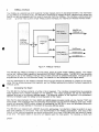
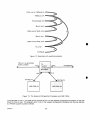
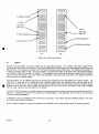
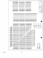
Figure 1: The IMS 8014 board
2
The IMS 8014
The VMEbus is a popular parallel bus originally developed for M68000 processors. TRAMs are INMOSdeveloped processor modules, designed to a published specification [3]. The IMS 8014 brings these two
standards together by allowing TRAMs to be integrated into VMEbus systems.
The IMS 8014 is a 6U high standard-depth VM Ebus board (see figure 1). It provides space for up to eight
TRAMs (TRAnsputer Modules). The VMEbus interface is a slave interrupter which gives one INMOS serial
link and a reset port. The TRAMs may be connected together in any network using the IMS 8014's two
IMS C004 link switches.
The IMS 8014 can take a variety of TRAMs to give processing power of 7-80, MIPS and 32K-8Mbytes RAM
per processor (using current TRAMs).
The VMEbus interface is designed for low cost and easy programming and allows VMEbus master devices
to communicate with one of the TRAMs on the IMS 8014 at a maximum data rate of about 300Kbytes/s.
3
Introduction to the VMEbus
The VMEbus, originally proposed by Motorola, Mostek and Philips, is now an lEG and IEEE standard. It
provides a parallel 8, 16 or 32-bit bus with multi-master capabilities. Mechanical constraints are basically
those of lEG 297 (eurocard). The VMEbus is now very popular and hundreds of boards are available from
many vendors. The VMEbus industry is co-ordinated by VITA (VMEbus Industry and Trade Association) who
publish useful information and organise exhibitions, conferences and committes on standards. 1
1 The current VMEbus standard recognis-ed and the one to which the IMS' 8014 adheres is_ The VMEbus specification REV C.t [6].
IEC 821 is almost identical to REV C.1, however the new IEEE 1014 spec uses new text to describe the VMEbus and it is not yet clear
whether any of the differences between the IEEE spec and REV C.1 are relavent to the IMS 8014.
DRAFT
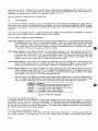
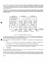
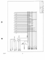
5
System VMEbus
• • • • d ...... M
. '••"
••••••
Slave:::V'rv1~~·qstt6reff~d~:~:>.>~::>
to': se
.. rial;lihktaridCresetUi::::C:/'//':
"
Link and reset
connections
to other boards
and systems
-
'
...
,.
"',"';"""'.'
L
iiiiil(i;li
.......
::
from P2 and " , - . . .
front p a n e l _
;., . . .
Y
_
~
Configuration
/system.
Figure 2: 810ck Diagram
3.1
VMEbus Terminology
The VMEbus Specification includes many special terms and abbreviations. These make descriptions of
VMEbus boards and systems very precise. Unfortunately for the casual user, some of these terms must be
defined in order that the description of the IMS 8014 ' s VMEbus interface can be preciseThere are different kinds of VMEbus data transfer cycle. The only cycles supported by the IMS 8014
are called "A 16:D08(0)". This means that a 16-bit address is decoded (sometimes called short I/O
addressing), and that 8-bit data is transfered on the lower part of the basic 16-bit databus. The
IMS 8014 neither monitors nor drives the higher address lines and the higher databus bits.
2 The VMEbus supports "indivisable" read-modify-write cycles, these are called RMW cycles. The
IMS 8014 does not support RMW cycles.
3 Devices which can interrupt the VMEbus are called "interrupters". The IMS 8014 is such a device.
There are seven VM Ebus interrupt lines. Since the IMS 8014 can use any of the seven lines, it is
called an "INT(1-7)" interrupter.
Exhaustive definitions of these and the other VMEbus terms are to be found in [6].
3.2
VMEbus Certification
INMOS has comitted to having the IMS 8014 and all future VMEb~s boards validated by VMElaboratories
. Inc. Denton, TX. The validation process ensures that a board has no design errors in the VMEbus interface
section and will work in any VMEbus system.
At the time of writing, the IMS 8014 has not been submitted for validation, contact INMOS for up-ta-date
information.
DRAFT
6
0
4
Transputer Background
The family of transputers available from INMOS includes 16 and 32-bit processors. These are all capable
of communicating with each other and can be programmed when connected together to execute tasks in
parallel. Full information on transputers can be found in The Transputer Reference Manual and in other
INMOS publications. The IMS 8014 uses one transputer on-board for network configuration and can, of
course, support transputer arrays in the form of TRAMs.
4.1
INMOS Links
Transputers use special serial communication connections to talk to each other. These are called INMOS
links, or links. Links use two wires to send data in two directions between two transputers (or other chips)
at up to 20 Mbits/s. All communication between TRAMs on the IMS 8014, and between the TRAMs and the
VMEbus interface, is via links. For full information on links see the [2] and [4].
4.2
TRAMs
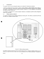
TRAMs are small circuit modules which communicate via INMOS serial links. A full TRAM background is to
be found in [3]. The smallest TRAM (called "size 1") is about 3~" by 1" and has eight le-type pins along
each of the short ends. These sixteen pins carry four INMOS links, reset signals, clock and power supplies.
TRAMs are plugged into a motherboard (or baseboard) just like socketed ICs.
pin 1 location
indicated by triangle
o
~
o
o
o
o
SLOTO
o
0:
(j:
Subsystem pin sockets
o
o
o
o
o
SLOT2
o
o
o
Adjacent slots . /
orientated in reverse
Figure 3: TRAM Slots
Larger TRAMs are simply a multiple of the size 1 footprint. Thus, a "size 2" TRAM occupies two of the sockets
into which a size 1 ·TRAM will plug. In order to avoid confusion,' discussions about motherboards (such as
the IMS 8014) al~ays refer to "slots" (see figure 3). A slot is one position into which a size 1 TRAM may be
plugged. So, for Instance, the IMS 8014 which has eight slots, may have eight size 1 TRAMS or four size 2
o,r two size 4 or one size 8 or even four size 1 and one size 4. There is no restriction on mixing the different
Sizes, as long as the total complement will fit.
.
DRAFT
7
In addition, some TRAMs have pins which are sockets at the top. This means that some TRAM combinations
can be "double-stacked". For instance, if you .had two size 4 (single transputer) TRAMs fitted to an IMS 8014,
only two slots would actually be used for the link signals. The remaining six slots would be covered by the
TRAMs but are not used electrically. In' some cases you can plug further TRAMS into the already fitted size 4
TRAMS and so make use of the unused slots. This double stacking is not always possible and usually makes
the board too high to fit into a single VMEbus card slot.
o
o
DRAFT
8
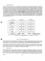
5
VMEbus Interface
The VMEbus is a parallel bus which supports multiple masters and 8, 16 and 32-bit transfers. Full infor,mation
on the VM Ebus is contained in [6]. The IMS 8014 implements a VMEbus SLAVE interface which allows one
INMOS link and a subsystem port (for reset) to be driven from the VMEbus. The interface is constructed and
driven
19 similar lines to other simple VMEbus slave interfaces, for instance an RS-232 interface board.
INMOS link
VMEbus Link
VMEbus~:
Interface
and buffers
~.,
~
~:~
4t'"
VMEReset
VMEAnal se
notVMEError
Figure 4: VMEbus Interface
The IMS 8014's VMEbus interface is an 8-bit slave, driven by some master VMEbus device. The master
can be any VMEbus board capable of generating A1S:008{O) VMEbus cycles. The IMS 8014 can generate
interrupts on any of the VMEbus interrupt lines or levels (the level is software-selectable). Interrupts can be
programmed to occur on link transmiter empty, link receiver full and subsystem error signal active.
The only parameters for the VMEbus interface which must be selected by switches or jumpers on the board,
rather than by software-programmed registers, are the VMEbus .address and whether the board responds to
VMEbus cycles.
5.1
Accessing the Board
The IMS 8014's interface contains a number of 8-bit registers. The interface is programmed by accessing
these registers from a master processor on the VMEbus. The master processor will see the IMS 8014's
registers as a part of its memory address space. The particular location of the registers in the processor's
~emory will depend upon the design and configuration of the master.
Note that the documentation for many 68020 and 68030-based processor cards will only mention "D3~" and
"016" cycles. This is because they are confusing the, processor bus size with the VMEbus cycle type. These
boards will generate 008(0) cycles, suitable for addressing ~he IMS 8014, when the processor performs a
byte access at an odd address in the sixteen bit bus size address space:
The IMS 8014 will respond with a 8ERR* (bus error) acknowlege if an attempt is made to perform an even
byte cycle (008(E)) or a 016 cycle. This is as recommended in the VMEbus specification. One result of this
feature is that incorrect programs and device drivers which try to read 16-bit data from the board will cause
a bus error. The action taken on bus error will depend upon the host system. For instance, a SUN-3 will
DRAFT
9
suffer a kernel crash. Programmers, especially those using high-level languages, should bear this in mind.
Programs running on a master board can be made to perform byte accesses either by writing sections in
assember or by specifying the IMS 8014's registers as type "char" in C.
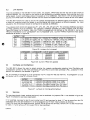
Figure 6 shows the registers and their active bits.
5.2
Link Interface
The IMS 8014's VMEbus interface provides one INMOS link, this is called the VMEbusLink. Unlike links on
transputers, which are directly connected to the processor, this link is connected to a special INMOS interface
chip called a link adaptor. This device (an IMS C012) functions very much like a UART does for an RS-232
-,
interface.
The IMS C012 link adaptor has four registers (see figure 5). These are all available in the IMS 8014's address
space and can be read/written by a master device on the VMEbus.
The link adaptor registers function as follows-
Input Data Register holds the last data byte received from the VMEbus link. It only contains valid data whilst
the data present flag is set in the input status register. It can not be assumed to contain valid data
after it has been read; a double read mayor may not return valid data on the second read. If the
data present flag in the input status register is valid on a subsequent read it indicates new data is
in the buffer. Writing to this register will have no effect.
0
Input Status Register This register contains the data present flag (bit 0, the least significant bit) and the
input interrupt enable control bit (bit 1, the second least significant bit). The data present flag is set
to indicate that a data byte in the input data register is valid. It is reset only when the input data
register is read, or by a link reset condition (see section 5.6). When writing to this register, the data
present flag and the unused bits 2-7 must be written as zero bits.
Output Data Register Data written to this register is transmitted out of the VMEbus link. Data must only be
written to this register when the output ready bit in the output status register is set, otherwise data
already bejng transmitted may be corrupted. Reading this register results in undefined data.
Output Status Register This register contains the output ready flag (bit 0, the least significant bit) and the
output interrupt enable control bit (bit 1, the second least significant bit). The output ready flag is
set to indicate that the data output buffer is empty. It is reset only when data is written to the output
data register; it is set by by a link reset condition (see5.6)
When writing to this register, the output ready flag and the unused bits 2-7 must be written as zero
bits. The output interrupt enable bit can be set and reset by writing to the input status register (note
that the output ready flag must be written as a zero). Interrupts are explained in section 5.5.
I Address I Register
#xxOl
#xx03
#xxOS
#xx07
Link
Link
Link
Link
adaptor
adaptor
adaptor
adaptor
input data register (read only)
ouptut data register (write only)
input status register
output status register
Figure 5: IMS C012 Registers
A link byte input proceeds as followsA data byte received on the VMEbus link sets the data present flag in the input status register. If interrupts
are enabled, a link data input interrupt is generated. A VMEbus master device (processor) will, either in
response to the interrupt or in a polling loop, examine the input status register. The data present flag will be
set, signifying valid data in the inputs data register. The master then reads the data byte. A new data byte
can now be received and the process repeats.
A link byte output proceeds as follows.
The master device (processor) either after receiving a data output interrupt or in a polling loop, reads the
output status register. It will determine from the output ready flag that a byte may be written to the output
J
DRAFT
10
o
#xx01
I I I
017
#XX031
016
0071 0061
015
I I I I I I
014
013
012
011
0051 0041 0031 0021 001
010
I
000
I
Link Adaptor
Input Data Register
Link Adaptor
Output Data Register
Link Adaptor
Input Status Register
Link Adaptor
Output Status Register
Sybsystem Error/Reset
Register
Analysj
#xxOB
SUbsystem Analyse
Register
Interrupt Enable
Register
#xxOF
#xx 11
#xx13
Lev21 LeV11 Levol
I I I I I I I I I
SI7
SI6
SI5
SI4
SI3
SI2
SI1
SIO
Interrupt Status/ID
Register
Err?
Err6
ErrS
Err4
Err3
Err2
Err1
ErrO
TRAM Error Register
Figure 6: VMEbus Interface Registers
DRAFT·
Interrupt Level
Register
11
data register. It then writes the byte to the output data register. The byte is transmitted on the VMEbus link.
When the link adaptor is next able to transmit a byte, the data output interrupt will be generated (if enabled).
5.3
Subsystem Interface
The VMEbus can provide "system services" to TRAMs (see section 7). This involves generating a reset
signal (VMEreset) and analyse signal (VMEanalyse) as well as monitoring an error signal (notVMEError).
This capability is provided via registers mapped into the IMS 8014's address space (see figure 7).
The subsystem interface register work as follows-
Subsystem Reset/Error Register Writing 8it" 0 of this register controls the state of VMEReset. Asserting
the bit (writing a one) asserts VMEReset (a reset condition). This bit is cleared on VMEbus reset.
Reading Bit 0 of this register returns the state of notVMEError. If notVMEError is asserted (error
condition) then the bit reads cleared (a zero).
The other unused bits must be written cleared (zero) and read as unpredictable values.
Subsystem Analyse Register Writing 8it 0 of this register controls the state of VMEAnalyse. Asserting the
bit (writing a one) asserts VMEAnalyse (an analyse condition). This bit is cleared on VMEbus reset.
The other unused bits bust be written cleared (zero) and read as unpredictable values.
An active revel on notVMEError can generate a subsystem error interrupt if enabled (see section 5.5).
I Address I Register
I
Subsystem Reset/Error register
SUbsystem Analyse register
Figure 7: SUbsystem Registers
Error Monitoring
5.4
The eight "error" signals from the eight TRAM slots on the IMS 8014 can be read in a register, available
in the IMS 8014's address space at location #xx13. Bit 0 (least significant) contains the error signal from
TRAM slot 0 and so on. If an error signal is active (signifying an error condition) then its corresponding bit
in the TRAM error register is cleared. These error signals are visually monitored by LED indicators (see
section 7.1).
Note that the contents of the TRAM error register need not bear any relation to the state of the SUbsystem
Error Register since they are derived from independent sources.
Note that transputers do not typically clear their error signals on reset, a program which explicitly clears the
error signal must be run. Transputer programs usually have this code included automatically. ..
5.5
Interrupts
The IMS 8014 can generate a VMEbus interrupt on any of the seven levels, the level is programmed into a
register. An interrupt can be generated by three conditions1 A data output interrupt from the link adaptor.
2 A data input interrupt from the link adaptor.
3 An active level on the subsystem error signal (notVMEError).
All three interrupt sources are independently maskable via the interrupt enable register. Note that for data
interrupts this is in addition to the interrupt enable bits in the link adaptor inpUt/output status registers.
DRAFT
12
e
When a VMEbus interrupt is recognised and serviced by a VMEbus "interrupt handler" (usually a processor),
the IMS 8014 responds with a status/ID byte. This is VMEbus terminology for "interrupt vector". The status/ID
byte will be used by the interrupt handler to determine what action to take in servicing the interrupt. The
status/ID byte returned by the IMS B014 is stored in the status/ID register.
I Address I Register
#xxOD
#xxOF
#xxll
Interrupt enable Register
Interrupt Level register
Interrrupt statusll D register
Figure 8: Interrupt Registers
The interrupt registers function as follows-
Interrupt enable register This contains three enable bits, one for each of the input data, output data and
error active interrupt sources. After an interrupt condition has occured, an actual interrupt will only
be generated if the appropriate enable bit is set.
If the' interrupt enable register, or the interrupt enable bits in the link adaptor input and output status
registers are used to disable an interrupt after that interrupt has been generated, and before the
interrupt acknowlege cycle, then the IMS B014 will not respond to the interrupt acknowlege cycle.
This will result in a bus timeout and probably some kind of spurious interrupt trap on the interrupt
handler.
t
The enable bits may be read. The unused bits in this register read unpredictable values. On VMEbus
reset all three bits are cleared, meaning that interrupts are disabled after a system reset.
Interrupt Level register This contains the VMEbus interrupt level to be used for interrupts. Seven levels
(1-7) are possible. The level used is dependent upo'n the system into which the IMS 8014 is
installed. Bits 0-2 hold the level, as a binary number. If a level corresponding to zero is selected
then interrupts will not be generated. This register must not be changed when interrupts are active.
The level can be read. The upper five bits return unpredictable data. The level is set to zero on
VMEbus reset.
Interrupt status/ID register This register holds the status/ID byte returned on interrupt acknowlege cycles.
This register can be read. On VMEbus reset this register contains unpredictable data. This register
should not be changed when interrupts are active.
The particular number stored in this register depends upon the driving software and the host system.
The IMS B014 will operate correctly with any status/ID byte.
A
'9
It should be noted that there may be interrupt conditions valid when interrupts are disabled. For instance, the
sybsystem error line could be permanently active or a byte may have been received by the link adaptor some
time in the past (possible due to electrical noise during power-up). Before enabling interrupts the programmer
should always check for pending interrupt conditions and if necessary, remove the condition. In the case of
a data input interrupt reading a byte from the input data register will remove the condition.
VMEbus Reset and link reset
506
The VMEbus defines a signal (SYSRESET*') which is used-to reset the entire system, usually after power-on
or a system crash. The IMS B014 uses this signal to do the following• The VMEbus interface is reset to a known state, certain registers are initialized to known values..
The IMS C012 link adaptor is reset, overcomming any locked up link condition.
• The IMS C004 link switch devices are reset, this disconnects all their link connections.
• None of the TRAMs are reset, the network configuration processor (T2) is not reset.
Throughout this document, this condition will be called "VMEbus reset".
DRAFT
13 .
When the VMEbus subsystem reset signal is asserted (by writing the appropriate values into the subsystem
reset/error register), apart from reseting any TRAMs connected to the VMEbus subsytem port, the VMEbus
interface link adaptor is reset. This allows link lock-ups to be overcome without totally resetting the entire
system. Users must bear this in mind as it means that while VMEreset is held active, no VMEbuslink
communication can occur. Also, after performing a VMEbus subsystem reset, the contents of the link adaptor
registers will need to be re-initialized.
VMEbus Interface Configuration
5.7
The IMS 8014 can r~spond to addresses in the A16 (short I/O) VMEbus address space. This means that
the board will respond to addresses in the ra'1ge #xxOO to #xxFF where xx is determined by the address
selection switches. In addition, the VMEbus interface can be completely disabled by removing jumper JP2.
This is useful if more than one IMS 8014 is to be fitted into a system and the VMEbus interface is not required
on all the boards. Full information on how to configure the board ·is to be found in section 9.
5.8
Address Modifier Codes
The VMEbus uses extra "address lines" called address modifiers to specify certain things about data transfer
cycles. The IMS 8014 as shipped responds to codes #29 and #2D. These correspond to the standard nonprivileged and privileged short address codes. If other codes are required for special applications, consult
INMOS for the appropriate information.
5.9
Programming the VMEbus Interface
Th,js section gives example code fragments in C to give a flavour of how the IMS 8014'5 interface may be
programmed. An undrestanding of the C language is assumed.
Firstly, we declare pointers to the registers-
char
char
char
char
char
char
char
char
char
char
char
char
*board base;
*data in;
*data-out;
*status in;
*status-out;
*reset;*error;
*anal.yse;
*int enable;
*int-leve.l ,.
*vector;
*tram_error;
void setup_addresses()
{
=
board base
OxOOff0001;
data in
board base;
data-out
board base + 2;
status in
board base + 4;
status-out
board base + 6;
reset ~ board base-+ 8;
error
reset;
ana~yse
board base + 10;
int enabl.e
board base + 12;
int-level.
board base +14;
vector
board base + 16:
tram_error
board base + 18;
=
=
=
=
=
=
=
=
=
=
}
Here are some example setup routines-
DRAFT
14
void enab1e out ints()
-
{
-
=
*status out
Ox02;
*int_enab1e 1= Ox04;
}
void enab1e in ints()
- -
{
=
*status in
Ox02;
*int enab1e 1= OxOS;
}
void enab1e_error_ints ()
{
*int enab1e 1= Ox02;
}
void disab1e_out_ints()
{
=
*status out
OxOO;
*int enab1e &= Oxfb;
•
void disable_in_ints ()
{
*status in = OxOO;
*int enable &= Oxf7;
}
void disabl.e_error_ints()
{
*int enabl.e &= Oxfd;
}
void set int
int l.eveI'; {
int level
~eve~(~eve~)
= (char)
level;
void set_vector(vec)
int vec;
{
*vector = (char) vec;
Polled link 110 procedures-
char read link ()
{
whil.e ( (*status in & 1)
return ( *data_in-);
-
1-
1)
}
void write link(byte)
char byte;{
whi1e ( (*status out & 1)
*data out
byte:
=
DRAFT'
.
!= 1 )
15
5.10
Operating without the VMEbus interface
The IMS 8014 has been designed so that correct operation of the TRAM slots is possible even if the board
is not connected to a VMEbus backplane. What this means is that the VMEbus interface is completely
independent of the TRAM slots, except for the VMEbus SYSRESET* signal. Since SYSRESET* is used for
power-on initialization of the IMS C004s, non-VMEbus users of the IMS 8014 should drive SYSRESET* with
their power-on reset signal. Except for this consideration, all the other VMEbus signals can be un-driven and
un-monitored and the non-VMEbus parts of the IMS 8014 will function.
I,n this non-VMEbus role, the IMS 8014 can b'e used as a double-eurocard TRAM motherbaord suitable for
mounting in standard VMEbus card-cages (which are readily available fitted with power supplies).
o
DRAFT
16
6
TRAM slots
The IMS 8014 has eight TRAM "slots". A slot is a place on the motherboard where a TRAM may be plugged.
A slot has four links associated with it. Since TRAMs come in various sizes, the number of TRAMS on a
motherboard may be less than the number of slots.
6.1
TRAM Network
The eight TRAM slots provided on the IMS 8014 each have four INMOS links. These links are designated
by their slot number and link number for the slot. Thus, slot 0, link 1 is link 1 of slot o. Slots are numbered
0-7, links are numbered 0-3. This numbering scheme is used consistently throughout this manual. The slot
posititions are shown in figure 1 and on the board silk screened legend.
,.All links 0, 3
Slot 0, link 0
optionally to
secondary
switching
~
~
~r:- Slbt1··
Slot 0'
'Slot'S
,:.;
,'<5 lot7
,',
\..
"""
:.
.:
".
'.'.'
16 links to front panel
:
:.
~1}y
•
M
{
~
r
All links 1,2
.<'.;
:.;
,':
,','
Figure 9: Basic Link Network
DRAFT
SIot 0, link 1
optionally to
secondary
switching
17
The eight slots, each with four links, give 32 links in total. The IMS 8014 uses IMS C004 link switch chips
to allow these links, along with INMOS links which come from the IMS 8014's connectors, to be cOflnected
to each other. The links are used to send data between the transputer on the TRAMs and so the actual
connection network used will be different for different applications. The basic network organisation is shown
in figure 9.
The IMS 8014 is capable of implementing any network between its eight slots. For instance, one application
may need a mesh array, shown in figure 10 wheras another may need a tree network (see figure 11).
~...in_k_.-t'~:. SlotO.
VMEbus.....
,.',':'
:-:
',':
Network can extend to other boards
via edge connector links
Figure 10: Example Matrix Network
All the connections made using IMS C004s are programmed by software, without the need to plug jumpers on
the card. The connection arrangement can be changed without the card being removed from the card-cage
and, with the right software it is even possible to change the connections dynamically (see section 6.7).
Some connections must be programmed by changing jumpers. These are connections which will carry data
involved in actually configuring the IMS C004s. Obviously, if a TRAM in slot 0 is to configure the IMS C004s,
it must communicate with them. The link carrying this communication can not itself go through either of the
IMS C004s. The link configuring done by jumpers is called "secondary link switching" and is described in
section 6.2.
The link connections and IMS C004 switches provided on the IMS 8014 allow any network to be constructed
between the TRAMs on the board. This is provided that the actual link used for any path between two TRAMs
is not fixed. For instance, to connect between slot 0 and slot 1 there is a path for each link on slot 0 to get to
a link on slot 1. However, if one considers slot 0, link 3 it may only be connected to links 0 and 3 on slot 1,
and not to links 1 and 2. Usually this restriction is not a problem as the links are physically identical and the
program running on the TRAMs may be written to use any link for a particular path.
There are a total of 24 links provided on the connectors so any multi-board network which nee'ds 24 or fewer
links off each board can be constructed. The connector links may be connected to any TRAM on the board
with a similar restriction on the actual destination link as for inter-board connections.
6.. 2
Secondary Link Switching
Some links which may be required to carry data for configuring the IMS C004s, but nevertheless themselves
require configuration, are switched by jumpers. Figure 12 shows the links involved. The grey lines indicate
a possible connection. The nine possible connections are designated A-I, by letters in the diagram. These
letters correspond with the letters in figure 24 attached to the jumper locations. If, for a' particular letter, the
DRAFT
18
Link to VMEbus
....
...................................
:-:·:-:-:·s····:r···:-:-:t··-:·:7·······;·:-:-··
}{~;. ..O}:
»){.
......
'
"
'
.................
:-:.:.:_:- ~~:~:~: ::::-:-:::<-:: ~~:-: ~> >:
,0
(not 'used)
Links to other boards via edge connectors
Figure 11: Example Tree Network
two jumpers are fitted then that connection is made. Care should be taken not to make mutually exclusive
connections 2 , for instance connecting A as well as I.
6.3
The IMS C004
The IMS C004 device used to switch links on the IMS 8014 is described fully in The Transputer Reference
Manual ([2]). The IMS C004 has 32 link ports. Any of these links may be "wired up" to any of the others
on commands sent to the IMS C004 down a 33rd link, called ConfigLink. The commands sent down the
ConfigLink are simple two or three byte messages, saying "connect link 1 to link 3" and so on. The ConfigLinks
for both of the two IMS C004s on the IMS 8014 are connected directly to two links of an IMS T212 (or
IMS T222) transputer which is also on the IMS 8014 (see figure 13). The IMS C004 control sequences are
shown in appendix K.
This transputer (called the network configuration processor or T2). sends the configuration data to the
IMS C004s based on commands which it receives on one of its other links.
6.4
Network Configuration Processor
The Network configuration processor is a 16-bit transputer (either an IMS T212 or IMS T222) whose purpose
on the IMS 8014 is to co-ordinate the flow of configuration data to the IMS C004 link switch chips. For easy
reference, this processor is also called a "T2". It has no external memory and is connected via links as shown
in figure 13. .
In general the Network Configuration Processor will run a simple program (which is booted down its link 1)3.
That program will then receive commands on link 1. These commands will come from some master computer
which may be setting up the network for a number of motherboards. The T2 will send any appropriate
configuration data to the IMS C004s on its links 0 and 3. Data which is not ~estined for its board will be
2Links are of course point-ta-point connections so the effect of installing jumpers in exclusive positions will be to connect two outputs
to each of the mo link inputs involved. While this will result in a non-working link connection, it will not damage any circuitry.
3Transputers do not need ROMs since after reset they can receive a program directly down a link and run it.
DRAFT
19
C004 link for VMEbuslink . .~ ~ ~___
VMEbus Link ~~.::;=
P4 Connector link -!llIlII"~~Slot 0:' Ii nk 0 -1IlIll1I!!~~~
C004 link for SlotO, linkO . . . .~~--
Slot 0, link 1
C004 link for SlatO, link1 "888S8lJl",~P9"""'""
T2, Link 1
ConfigUp .....~~Figure 12: Secondary link switching jumpers
T2Link1, to secondary
switch jumpers
T2.;·.·::::·
n·etW()'r~(~':.:-... .':
:.:. :C9nn99r~~:i9n
CanfigDawn
~---------~
::···.·Pr.():c~~§()m
ConfigLink
IMS·C'Q04(A)
Figure 13: The Network Configuration Processor and IMS C004s
re-transmitted on link 2. This data will be received on link 1 of the network configuration processor on the next
board (if there is one). The program which runs on the network configuration processor can be user-defined,
but INMOS supplies suitable software.
DRAFT
20
The two links 1 and 3 of the network configuration processor are designed to be connected as a daisychain in multiple board systems. When links 1 and 2 of the T2 reach the edge connectors, they are called
"ConfigUp" and "ConfigDown" respectively. In general, ConfigUp of each board is connected to ConfigDown
of the adjacent board. ConfigUp of the first board is connected to the processor which is configuring the
network (see figure 14).
The reason for using a processor to communicate with the link switches is that infinitely large multi-board
systems may be constructed. Such systems may be configured from one link (the head of a large ConfigUpConfigDown daisy-chain) and may contain different board types since all INMOS TRAM motherboards use
the same scheme.
1st board
I
2nd board
,:',:
VME interface
r1
Slot 0
I
~M
-y
»
:.;':
3rd board
,'::
le
'::'
0OL.LII
Al',",'
'C,",',',','
I
CO 04
C004
C004
','
7
,':
T2
T2
T2
<::.
,',
/'0
ConflgDown
"
ConfigUp
/'
ConfigDown
ConfigDown
next board
~to
'\
ConflgUp
Figure 14: ConfigUp/ConfigDown Daisy-Chain
The IMS 8014 provides flexibility in the connections to the T2. This is achieved via the secondary link
switching jumpers (see figure 12) and jumpers which allow either the front or the back edge connectors to be
u~ed for ConfigUp and ConfigDown (see section 9 and figure 17).
With the secondary link switching arrangement on the IMS 8014, it is possible to send configuration data to
the T2 from1 Slot 0, Link 1-This means that a "master" TRAM on the IMS 8014 can configure the TRAM array.
I
2 The VMEbusLink-This means that a VMEbus master can configure the TRAM array_
3 The "ConfigUp" connections on the edge connectors (either the front or back of the board, selected
by jumpers)-This means that some other board can configure the TRAM array.
6.5
C004 Reset
The two IMS C004 link switches have a reset pin that is driven by a power-on-reset circuit. The IMS C004s
can be also soft-reset by a command from the T2.
The IMS T212 has 2 Kbytes of on-chip RAM (4 Kbytes in the case of the IMS T222). It also has an external
memory interface. Circuitry on the IMS B014 is connected to the T2's external memory interface which allows
the reset signal to the IMS C004s to be controlled from the T2. By writing a one into bit position zero in any
DRAFT
21
external memory word, the reset signal to the IMS C004s is asserted. Similarly, by writing a zero into bit
position zero in any external memory word, the reset signal to the IMS C004s is de-asserted.
The porpose of this feature is to allow the C004s to be hard-reset without resetting the whole VMEbus system.
This may be useful in systems requiring some kinds of fault tolerance. Note that if the IMS T212 reads from
any location in its external memory space then the IMS C004 reset signal will be set to an unpredictable level.
6.6
Affect of the IMS C004 on link bandwidth
Depending upon the type of transputers on the TRAMs at both ends of a link which passes through an
IMS C004, the link bandwith may be lower than for a simple transputer-to-transputer connection.
For instance, two IMS T800s connected directly will give a unidirectional link bandwith of 1.7 Mbytes/s.
However, with one IMS C004 switching that link, the link bandwith is 1.3 Mbytes/s. With two IMS C004s
swit~hing the link, as is the case with a board-to-board link using IMS 8014s, the link bandwith will be
800 Kbytes/s.
If an application calls for full link bandwith and this is not achievable using the IMS C004s then, providing the
desired network does not need to change, header-circuits can be plugged in place of the IMS C004s. These
will connect the links across directly using pieces of wire and buffer chips where necessary. Contact INMOS
for information on these.
6.7
Dynamic Connection Changing
In theory it is possible to change the configuration of the IMS C004s while a program is executing on the TRAM
array. This may be useful, for example, in a system which needs a particular network during a data gathering
phase but a completely different network during a data processing phase. Although this is possible, it is not
easy to organise and should only be attempted by experienced users who have a complete understanding of
what needs to be done. For those who still want to pr0geed, here are some guidelinesThe basic idea is that providing there is no traffic on a link, you can switch the path it takes through an
IMS C004. After switching, processing can proceed using the neLw network.
Obviously this requires careful synchronisation between all the programs in all the TRAMs-something which
is usually achieved via the links which are being switched.
DRAFT
22
,
7
System Services
Transputers and TRAMs need to be fed reset and analyse signals (these allow the processor to be reset and
placed in a debugging mode) and they generate an error signal which needs to be monitored. These three
signals (reset, analyse and error) are together called system services. The system services for any TRAM
are treated as one conceptual signal, even although there are actually three. System services are generated
by a "subsytem port". A subsystem port will generate a reset and analyse sugnal and monitor an error signal.
The VMEbus interface of the IMS 8014 provides a subsystem port. Some TRAMs also have subsystem ports.
(in this case, the TRAM is said to have subsystem capability) on three extra pins (see section 8.3). Slot 0
of the IMS 8014 can take a TRAM with subsystem capability. System services are used by TRAMs. On the
IMS 8014, slot 0 is separated from the other seven TRAMs for system services-this is to allow the TRAM
in slot 0 to provide the system services for the other seven. System services can also come from off-board
via the ServicesUp connection on the connectors. The system services going to slots 1-7 are propagated
to the ServicesDown connection on the connectors-it can provide the ServicesUp for the next board in the
card-cage (see figure 15).
1st board
3rd board
2nd board
0
••.
.
:'
,-
.
: .•...
.
-
0:·•.••.
: ~.:
...
..
.. . -
.
.....
·····0······0········
)
...........•••...•..•..........• :•. •••..
....
....
','--'
«~>~_-:
-
-
. ..
.
.
".".',-,',"
"
.
.
,.
.,
-
.
-,
'--
.,.
.
',
.
:.....
."
,'..
'.'
.
-.
~'.
,
~~ ..
....
..
:. . .
-.
.
..
~
········'·0····················.·······::··.···.·.
·• ··0···········.···•.•·. . ·. ·•:. · ·.,· ·.
·
.
..•.••..••••.
::0····:·······.········:":>-·. ·.·0·"·
. · · .· : · · '.: :. •.:
. . ','.
.,.
'.-
·
.
'
..
~
.-,
.
-'.
- -'. .',-.- , -:. .. ..' . ',' -:.. <: '. -: :-: -: -:
"",'.-'.
::":,'..
,
:/.~.: .
.
.'...
-,
....:/:-:.:
..--.
.. .
.-
.
.,
.
····0·····.·:.········.····0···. ':· :· · .,: :.
:
'. '
:.::; ..
.
·. .
=::,
-
.
-.,
<-: ...
. ..
.
::...:... :•....::=;::.. «.:.. ::.:.:..
.
<;
-
~.
-
.
•. ,::>.>::-...\ •. ::::<::
.
--.-.
:<-'
'
: . ~
..
-_
-.
.. - .
~: ~ .: .. '
:::.
'-
,-
(0···.:.·····0·...:.•. .•:. .•
·······:··'·:··:.············0·····:···.··.····.:.:·'
::
::: ::::, ::. •:.
0
~:
..
-
.
-
...
.'.
'
_. -
.
;:- .' ....:.:><: :~: -: . .:-:. -:<'-.,'.:,:.'- :.::-: <.' .:.: .-:. .:-. :. >: - . . .. ..:-. . '..
.---.,."
.. -
.
..
-
._.
~.::~:~<:::::.
~::'~·:···:··········:·········.>·····.··0····.:·.:.:
. ·:•' ·0···
.. ···.:··:.:···•.:><::'.
:···· . '
~:,:~~~-~.;~.
.
:~':~.
:.~::~.';>':
".'
.'
ServicesUp
o
Figure 15: Services Daisy-Chain
These ServicesUp and ServicesDown connections on the edge connectors are designed to allow multiple
board systems to be connected together in a daisy-chain. That is, the ServicesUp for a board comes from
the ServicesDown of the previous one. These connections are compatible with other INMOS boards.
The arrangement of system services connections is shown in figure 16. The "switches" shown in the figure
allow the user to select where the system services for parts of the board are driven from. In reality, these
switches are electronic and are controlled by jumpers-one jumper per switch (note that in figure 16 the
switch positions correspond to the respective jumpers being "installed").
7.1
Error LEDs
There are eight LED indicator lamps situated along the middle of the IMS 8014's front panel. These monitor
t~e error s!gnals from all eight slots on the board. This monitoring is completely independent from the error
signals which go to the connectors and to either of the "subsystem" ports-those error signals are combined
from a number of slots. When the board is fitted in a card-cage the top LED monitors slot 0, the next lower
slot 1 and so on down to slot 7 at the bottom. These LEDs are useful for error diagnosis because they allow
DRAFT
23
JP8
VMEbus:;
Subsystem
o
Subsystem
BackServicesUp
----0
FrontServices Up
JP9
0 ' - - - - BackServicesDown
FrontServicesDown
JP10
Figure 16: System Services Configuration
errors to be tracked down to an individual TRAM after an error is detected by one of the subsystem ports.
Full information on the transputer error signal can be found in [2]. Note that error signals are not usually
de-asserte-d on reset so these LEDs may be lit when the board is switched on.
7.2
Driving Services Signals
The three services signals-Reset, Analyse and Error- are detailed in [2]. However, because the signals
are passed through circuitry on the IMS B014, it is necessary to allow time for the signals to be propagated
through the system. Always allow 100ms between the assertion of a services signal and the time when it
actually reaches its destination.
· DRAFT
·24
Front ConfigUp (P4)
ConfigUp
to secondary link
switch jumpers.
~~~~~~~~~~~~_~ K~K12
Back ConfigUp (P2)
~
Front ConfigDown(P5)
ConfigDown
direct from T2 Link2
~
---
K1-K6
Back ConfigDown (P2)
9_~~~~~~~~~~~~
~
Figure 17: ConfigUp link switching
P3
Figure 18: Position of P3 and GND point
DRAFT
2~
8
Connectors
The IMS 8014 has five connectors. Two of these are the VMEbus P1 and P2 connectors (these designations
match those in the VMEbus specification). Another two connectors are on the front panel and are called
P4 and PS. The remaining connector (P3) is a four-pin power connector. P3 allows the ±12v power rails
from the VM Ebus to be used by TRAMs, for example the IMS 8407 Ethernet TRAM which needs +12v. The
position of P3 is shown in figure 18. Mechanical details for the connectors are given in section C.
4 links
~
4 links
P2Link1,3,5,7
o
BackServicesUp
BackServices Down
Figure 19: Back Connector (P2)
When signals other than the VMEbus are to be connected to a VMEbus board there are two possibilitieseither use the uncommited P2 pins (see below) or connectors on the front panel. P2 connections are
mechanically neat but are difficult to access in a card-cage and'give only 64 pins. Front panel connectors
are easy to access but are too untidy in some applications. The IMS B014 allows either approach to be
used. Either the front connectors (P4 and P5) or the rear connector (P2) may be used. Provision is made for
configuring some signals to connect via either the front or the rear connectors.
The VMEbus defines all of the pins on P1 and 32 of the 96 pins on P2. Since the IMS 8014 does not support
any of the 32-bit VMEbus capabilities, the VMEbus-defined pins on P2 are un-connected, except for power
pins. In order to function on a VMEbus, only P1 need be connected-to a J1 VMEbus backplane. If the
full power dissipation of the IMS 8014 is to be realised then the power connections on P2 will need to be
conected to a J2 backplane.
The remaining 64 pins on P2 which the VMEbus does not use (these are user-defined in the VMEbus
specification) are, on the IMS B014, used to carry INMOS links and reset signals to other boards in a cardcage. Note that if conections to P2 are inconvenient then connectors P4 and P5 can be used for any signal
which is available on P2 (indirectly in the case of links).
The user-defined pins on P2 are used by many VMEbus boards to take I/O signals out of the card-cage and
also to carry "secondary" busses such as VMX and VSB. Because of this, some card-cages may have these
pins pre-wired. It is important to ensure that the IMS 8014 is not plugged into a card-cage which has these
signals wired for a different board (see section 8).
DRAFT
26
o
.. ...
.
.....,
<'
___-'c.·
/.,.......~
___-'ct
FrontServicesUp
fr
...
~-
(-',,-_
Slinks
j/",-'----'
••• 4 •••• · _ . _ . · •• _
P4LinkOP4Link7
~~) ....
' .....~~-,:F}
t:.-..'~~
/>",-'---~
1/:-
:{:I
[}
~>I
.
,
~
:f<,,-'
FrontConfigUp
.
,('
".'
<,,-'----'
<,,-'----'
--_.....,.
It
------
Blinks
PSLinkOPSLink7
(:,"-- - - - '
r
ConnectorLink
.
<",-'_.-......
FrontConfig Down
FrontServicesDown
L
P4
PS
Figure 20: Front Connectors
8.1
Cables
INMOS has developed a standard cable set for evaluation boards. Link cables have 5-pin single-in-Iine
connectors at each end with a key pin. Services cables have S-pin single-in-line connectors at each end with
two key pins. The keyed pins prevent the connectors being inserted incorrectly. The cables are available in
a range of lengths (see fig 39). Using this system it is quick and easy to connect links and services signals
from board to board and system to system. These cables must not be used between equipment on different
mains circuits and ideally, to ensure noise-free operation, should only be used within one system operating
from the same SV power supply.
e
-
The connectors on all INMOS boards and modules are designed to be compatible with these cables. The
IMS 8014 is provided with a cable set which includes many short link cables (which can be used to link
edge links to each other), some standard and long link cables (which can be used to connect multiple boards
together). some services cables (reset, analyse and error) and a DIN 41612 connector which when plugged
into P2 allow cables to be connected to the board.
This DIN 41612 connector is a back-ta-back plug with some pins cut short and some pins sleeved (shown in
figure 21). These are to mate with the keying on INMOS cables. This assembly fits onto P2 or onto the back
of a J2 VMEbus backplane.
A "breakoutU plug is provided for P4 and PS (see figure 22). This allows standard INMOS cables to be used
with these front panel connectors.
If extra INMOS cables are required, contact either INMOS or your local Sales Office for ordering details.
DRAFT
27
--p[Lc:J
::.=
~
<:.:
~.r:::·.
o
I.'''_I.·':-:''::· ..·
Figure 21: "Back-ta-back" DIN Connector
o
FrontServicesUp (on P4)
Link 0
Link 1
Link2
Link 3
Link 4
Link S
Link 6
Link 7
FrontConfigUp (on P4)
Connector Link (on P4)
not used
Front ConfigDown (PS)
not used
FrontServicesDown (on PS)
Figure 22: Front Connector "breakout board"
DRAFT
28
9
Configuration
This section covers all user-configurable aspects of the IMS B014-switches and jumpers.
Jumpers are labeled either JPx, where a jumper is either installed or absent between two pin posts; or
Kx-Ky where jumpers are installed over a centre pin and either of two other pins (making a kind of changeover switch). The locations of all the jumpers are shown in figure 24. It is not necessary to wire-wrap any
connections between jumper pins.
The IMS 8014 is shipped with no jumpers installed-therefore it is necessary to perform some configuration
before using the board.
9.1
VMEbus address selection
The VMEbus interface can be completely disabled by removing JP2. This means, of course that JP2 must
be fitted for the VM Ebus interface to work.
10
Figure 23: VMEbus address switches
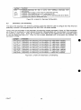
The V.MEbus address is selected by two hex switches (see figure 23). In setting the VMEbus address, you are
selecting a unique 8-bit binary number which will be compared with the VMEbus addresses. The upper four
DRAFT
29
bits of this number are set by SW2 while the lower four bits are set by SW1. A small screwdriver or trim-tool
can be used to rotate the pointers on SW1 ,2. The pointer must be rotated to the desired hex character. Here
are some example settingsWe want to use addresses #DBOO-#DBFF. This means that the 8-bit number to be compared is lOB. Its
upper four bits are #0, its lower four bits are iB. Accordingly we set SW2 to "D" and SW1 to "B".
K6,K5,K4
K7,K8,K9
K10,K11,K12
JP1
JP3
JP4
JP5
JP6
JP7
A
B
C
D
E
F
G
H
I
0
000
000
000
000 10 01
00
00
00
00
00
00
00 00
00 00
00 00
00 00
00 00
00 00
00 00
00 00
00 00
Figure 24: Configuration Jumpers
DRAFT
30
00
00
00
00
JP2
JP8
JP9
JP1Q
JP11
JP12,13
JP14,15
JP16,17
JP18,19
JP20,21
JP22,23
JP24,25
o
9.2
Link Speeds
The links available on the IMS 8014 (from C004s, link adaptor, TRAM slots and the T2) can be set to work at
different speeds. For a link port on one device to talk succesfully to another device, they must be set to the
same speed. Current technology allows link speeds of 10 or 20Mbits/s. Note that if a link is being switched
by one of the IMS C004 link switch devices then the C004 link speed must be the same as the link's speed.
The IMS 8014 allows the user to set the link speeds independently for different parts of the board. This isto allow for situations where the board is communicating with other systems at different speeds. For most
situations, the whole board would be configured to operate at 20Mbitsls.
The jumpers which control link speed are JP1 , JP3, JP4, JP5, JP6 and JP7. For complete 20Mbits/s operation
all these jumpers must be removed. For complete 10Mbits/s operation all these jumpers must be fitted.
Figure 25 shows the full details. Note that TRAM link speeds are not defined by the IMS B014, but by the
TRAM's interpretation of its "LinkSpeedA" and "LinkSpeedB" pins. Current TRAMs implement these speed
selections as shown in figure 26.
I Jumper I Use
1
JP3
JP4
JP5
JP6
JP7
In spee or
us In . nsta e or 1
ItS/S, empty or 2
ItS/S.
Link speed for C004s and T2. Installed for 10Mbits/s, empty for 20Mbits/s.
LinkSpeedA for TRAMslot o. Installed for "Iow", empty for "high".
LinkSpeedB for TRAMslot O. Installed for "Iow", empty for "high".
LinkSpeedA for TRAMslots 1-7. Installed for "Iow", empty for "high".
LinkSpeedB for TRAMslots 1-7. Installed for "Iow", empty for "high".
Figure 25: Jumpers for link speed
I LlnkSpeedA I LlnkSpeedB I Link 0 speed I Links 1-3 speed I
ow
low
high
high
ow
high
low
high
1
ItS/S
10Mbitsls
20Mbitsls
20Mbitsls
ItS/S
20Mbits/s
10Mbits/s
20Mbits/s
Figure 26: Current TRAM link speeds
9.3
ConfigUp and ConfigDown
The IMS 8014 allows the user to select whether the network configuration pipeline links (ConfigUp and
ConfigDown) connect to the front connectors (P4 and P5) or to the rear connector (P2). Jumpers K1-K12
perform this selection, as detailed in figure 27.
'4)
So, for example if ConfigUp is to be connected via P4, install K7-K8 and K9-K10. If ConfigDown is to be
connected via P2, install K1-K2 and K3-K4.
I Jumper
I Function
K1-K2,K4-KS
K2-K3,K5-K6
K7-K8,K10-K11
K8-K9,K11-K12
Installed-GonfigDown Goes to P2 (rear)
Installed-ConfigDown Goes to PS (front)
Installed-ConfigUp Comes From P4 (front)
Installed-ConfigUp Comes From P2 (rear)
Figure 27: Jumpers for ConfigUp/ConfigDown
9.4
Services
The services signals (reset, analyse and error) can be switched via jumpers JP8-11 as detailed in figure 28.
Figure 16 shows the services organisation.
If, for example, services for slot 0 are to come from P4 and services for slots 1-7 are to come from slot O's
subsystem pins and ServicesDown is to be propagated out P2 then install jumpers as followsInstall JP9 to set the ServicesUp source, remove JP8 to set slot O's services, remove JP11 to set the services
for slots 1-7 and remove JP1 0 to select P2 for ServicesDown.
.
DRAFT
31
JP9
JP10
JP11
Figure 28: Jumpers for Services Configuration
9.5
Secondary Link Switching
The idea of the secondary link switching jumpers is that they allow the user to configure the links which are
potentially involved in the programming of the IMS C004 link switch devices.
Various links are switchable via the secondary link switching jumpers, as shown in figure 12. Each connection
arc in figure 12 is lettered A-I. Each lettered connection has associated with it two jumpers in the secondary
link switching jumper block. These are numbered JP12-JP29 and are labeled with the connection letters
A-Ion the board (see figure 24). When the two jumpers associated with a connection are installed, the
connection is made.
I Jumper
JP12,JP13
JP14,JP15
JP16,JP17
JP18,JP19
JP20,JP21
JP22,JP23
JP24,JP25
JP26,JP27
JP28,JP29
I Function
Secondary
Secondary
Secondary
Secondary
Secondary
Secondary
Secondary
Secondary
Secondary
link
link
link
link
link
link
link
link
link
switching,
switching,
switching,
switching,
switching,
switching,
switching,
switching,
switching,
link
link
link
link
link
link
link
link
link
connection
connection
connection
connection
connection
connection
connection
connection
connection
"A" made when installed.
"8" made when installed.
"C" made when installed.
"0" made when installed.
"E" made when installed.
"F" made when installed.
"G" made when installed.
"H" made when installed.
"I" made when installed.
Figure 29: Jumpers for Secondary Link Switching
DRAFT
32
10
Example Setup
To help first-time users here is a complete example setup for the IMS 8014.
This configuration is typical for a system where the IMS 8014 is used to host a transputer development
system. A TRAM with subsystem capability is installed in slot O.
Starting with no jumpers installed:
1 The VMEbus interface is enabled by installing JP2.
2 All links are set to 20Mbits/s speed by leaving JP1-JP7 empty.
3 Install JP8 to generate system services for slot 0 from the VMEbus subsystem.
4 JP9 is left empty since its state is not important.
5 JP10 is installed so ServicesDown go to the front panel connector (PS).
6 JP11 is left empty so services for slots 1-7 come from slot 0'5 subsystem.
7 Install K2-K3 and K5-K6 so that ConfigDown goes to the front panel connector (PS).
(0
8 Install JP20 and JP21 so that slot 0, link
°
is connected to the VMEbus link.
9 Install JP28 and JP29 so that slot 0, link 1 is connected to link 1 of the nextwork configuration
processor.
1 0 Finally, configure the VM Ebus address switches to an address appropriate for your system.
DRAFT
33
A
Glossary
i"
16"
Jumper These are the little plastic blocks, about an
by ~"by
which are to be found in a small bag in
the packaging and also plugged into the card. They have a metal insert which shorts two pin-posts
together when the jumper is fitted to them. Fitting is accomplished by aligning the two holes in the
jumper with the two posts which it is to be plugged into; next push the jumper fully home. Removal
is usually best done with the aid of a small pair of pilers-it is possible to break your nails when
removing a jumper. Note that jumpers sometimes fail "open" so if you are suspicious, it may be
worth checking or replacing the jumpers on a non-functional board.
Card-cage The metal frame which holds a set of circuit cards (boards or PCBs) together. Usually has an
associated backplane and power supply.
VITA The "VMEbus Industry Trade Association" is an organisation of VMEbus vendors and users which
promotes the VMEbus and produces standards and literature.
IEC297 The mechanical standard which specifies the "eurocard" board sizes and corresponding card-cages.
RS·232 A "standard" asynchronous serial interface used for communication between computers and video
terminals and peripherals.
UART Stands for Universal Asynchronous ReceiverlTransmitter. This is a standard device, dating back to
discrete-transistor circuits in DEC computers, which provides an interface between an asynchronous A
serial communcation line (such as RS-232) and a TTL parallel port.
•
Link Lockup INMOS serial links use an interlocked acknowledge protocol. This means that if for some
reason an acknowledge packet is lost and does not arrive at the sending transputer or link adaptor
then no more communication will occur. This is because the sending device is perpetually waiting for
the acknowledge. The acknowlege packet can be lost due to noise (unlikely in a correctly designed
system) or cables becoming disconnected.
The only way to resolve a link lockup is to reset the link ciruitry in the devices at both ends of the
link.
DRAFT
34
B
Handling
The unpacking note in the shipping carton will give details on how to unpack the IMS 8014. Standard antistatic precautions should be observed since the IMS B014 contains MOS devices which are susceptable to
static-discharge damage.
Some VM Ebus compatible card-cages, notably SUN workstations, make use of the user-defined pins on
connector P2. It is extremely important that the IMS B014 is not plugged into such a card-cage because
-permanant destruction of the IMS 8014 and/or SUN can result. This restriction only applies to some slots in
some kinds of SUN (and probably other card-cages) but users should always be aware of the danger. The
solution required for the SUN is to use a special holding frame which isolates the P2 user-defined pins from
the backplane. INMOS believes that the frame required has SUN part number 501-1220. Contact INMOS if
you are unsure of the situation.
8.1
Installing the IMS 8014 in a VMEbus card-cage
Before installing any board, first make sure that the power is turned off.
Inspect the VMEbus connectors for bent pins. Next align the corners of the board with the ends of the
card-guides. The TRAM slot side of the board should be to the right. Slide the card home-if resistance is
encountered the board is probably not aligned properly with the card guides. Now push firmly on the handles
. until the board is fully home. The front panel will fit against the card-cage. Lastly screw in the retaining bolts
at the top and bottom of the front panel.
Remember that if you are using interrupts, the interrupt daisy-chain jumpers on the VMEbus should be
configured correctly. Please consult the documentation for your VMEbus system to find out how to do this.
8.2
TRAM Installation
Although TRAMs can be plugged and un-plugged from the IMS B014 many times without contact wear, great
care should be taken when fitting and removing TRAMS.
When fitting a TRAM to the IMS 8014, inspect the TRAM for bent pins, then make sure that it is the correct
way round (match up the yellow triangle on the TRAM with the yellow triangle on the IMS B014), then line
up the pins with their sockets. When you are sure that the pins are aligned, gently push the TRAM home.
Excessive force is not necessary and probably means that the pins are misaligned.
If vibration resistance is needed then you will need to bolt the TRAM in place using the M2.5 nylon bolts
provided with the IMS 8014.
TRAMs must be kept as flat as possible when they are removed from the IMS 8014. Gently ease up one end
of the TRAM a little, then ease up the other end by the same amount. Continue this until the TRAM comes
free from its socket.
.
If you are fitting a TRAM in slot 0 to run a transputer development system it is likely that you need to fit the
subsystem pins. Fitting a TRAM with subsystem pins is covered in section 8.3.
8.3
Installation of a TRAM with subsystem pins
Some TRAMs have a "subsystem" port (see section 7). The signals for the subsystem port come through
three extra socket pins (other than the standard TRAM pins) on the underside of the TRAM. When fitting a
TRAM which uses its subsystem port to a motherboard such as the IMS B014, you must install the special
pin-strip in the TRAM's subsystem pin sockets. This procedure is shown in figure 30. Some of these pin-strips
are provided with the IMS 8014. The TRAM is then plugged into the IMS 8014 in the same way as described
above in section 8.2, taking care to align the subsystem pins with their respective holes in the IMS 8014.
These subsystem socket pins on the IMS 8014 are shown in figure 31.
~ote that subsystem pins can only be fitted to a TRAM which has subsystem capability and which is plugged
Into slot O.
DRAFT
. 35
Main TRAM Pins~
TRAM pcb
Figure 30: Subsystem ~ns installation
Figure 31: Subsystem pin sockets
DRAFT
36
C
Mechanical and Thermal Details
The IMS 8014 is designed to accord with DIN 41494 and IEC 297 standards. The board is nominally 160mm
by 233.35mm. Figure 41 shows all board dimensions. Nominal board thickness is 1.6mm. The supplied front
panel width is 4HP (approx 20mm). This is compatible with a board-to-board pitch in a card cage of 0.8".
M2.5 fastening bolts are provided on the front panel, these mate with tapped holes in the card cage and fix
the board securely. Front panel handles allow the board to be removed from the card cage (by un-screwing
the retaining bolts and pulling hard on the handles). Note that the front panel is required when operating the
IMS 8014 in a card cage, both for mechanical rigidity and to give correct cooling air flow.
No components protrude more than 2.47mm below the surface of the board. To fit in a 0.8" pitch card-cage,
no component should protrude more than 13.7mm above the surface of the board. This is a function of the
TRAMs installed on the board.
Adequate cooling air flow must be provided to maintain the components on the board within their operating
temperature. Air flow should run parallel to the board surface and parallel to the front panel. The amount of
heat dissipated by the board depends upon the TRAMs fitted. With no TRAMs the IMS 8014 dissipates no
more than 5W. With TRAMs fitted, the maximum dissipation allowed (from 5v supply) is 18.75W when only
using a J1 backplane and 37.5W when using a J1/J2 backplane 4 . It is essential that the user ensures that
the maximum power dissipation is not exceeded. The cooling air flow required for a particular application will
probably need to be determined empirically.
<I
A single board operating in static air at room temperature (and not in a card-cage) will usually not need'forced
air cooling. This kind of set-up should only be used for lab and development work. High reliability is not to be
expected from boards which are not provided with adequate cooling. Some TRAM types may require forced
air cooling if they have high power dissipation components such 'as very fast PALs and fast A-D converters.
The two DIN 41612 (603-2-IEC-C096Mx~xxx) connectors (P1 and P2) have class 2 contact finish (1 micron
gold) and are specified to give 400 mating cycles minimum.
If a TRAM with special I/O capabilities (such as the IMS 8407 Ethernet TRAM or the IMS 8409 Graphics
TRAM) is fitted to the IMS 8014, consideration will have to be given to the TRAM's cabling requirements.
One way to handle cabling from TRAMs is to make a special wide front panel for the IMS 8014. Connectors
can be mounted through the panel and cabled via flying leads to the TRAMs. This gives a neat removable
unit but takes up card-cage space. A drawing of the hole positions in the IMS 8014'5 front panel is shown in
figure 40.
C.1
Mating Connectors
Connectors to mate with the connectors on the IMS 8014 are as followsP1/P2 P3 -
96-way DIN41612 female connectors which are available from most connector manufacturers.
Molex 8981/70156 series (Disk Drive Power Connection System), for instance shell 891-4P (order
number 15-24-4048) with crimps order number 02-08-1202.
P4/P5 -
D-subminiature 37-way female Connectors, available in solder tail, crimp and solder bucket form
from most connector manufacturers.
Jumpers -
0.1" pitch jumpers or programming shunts, again available from many manufacturers. Some
types are very stiff-fitting and suit fixed configurations, others are slacker and are more useful when
configurations are changed often.
Note that INMOS does not guarantee that these connector descriptions and part numbers are correct.
4 J1 is the minimum VMEbus backplane and mates with P1 connectors on VMEbus boards. J2 mates with P2 c;"nectors and is
sometimes called a 32-bit backplane because it is needed for 32-bit VMEbus operations. Combined J1/J2 backplanes mate with both
P1 and P2 and are needed for reliable operation of fast 32-bit VMEbus transfers.
DRAFT
37
Handles
Connector P4
Card-cage retaining
screws, bolt into
tapped strip on card-ca g•
lot 7
Error monitor
LEDs
Connector PS
/
Figure 32: Front Panel Identification
I. Storage
to +8 °
95% non condensing
< O.15°Cjs
-300 to +16000m
emperature
Relative Humidity
Thermal Shock
Altitude
Figure 33: Environmental Details
DRAFT
38
o
Electrical Details
0.1
Power Supply
The IMS 8014 requires power supply voltages in accordance with the VMEbus specification. That is, the +5V
dc supply must be between 4.S75V and 5.25V and have less than 50mV pk-pk noise and ripple between dc
and 10MHz. The IMS 8014 does not incorporate protection against incorrect power supplies. Major damage
can result from operating the board outside its power supply range.
Board-to-Board Link Connections
0.2
The INMOS serial links provided on the IMS 8014's connectors may be used to communicate directly with
other boards in the same electrical environment (same DC supply, ground reference and low electromagnetic
noise). However, these link connections must be made with transmission lines of characteristic impedence
100f2.
The following are examples of valid connection methods1 A printed circuit trace of about O.OOS" width over a ground plane on a multi-layer board.
2 Twisted pair ribbon cable.
"'0
3 INMOS link cables.
4. Twisted pair wire-wrap wire.
Single wires, PC8 traces without ground planes and coaxial cable should not be used. It is recommended
that link connections are not longer than 1m. Although long connections will function, enhanced reliability will
be gained by making longer connections using buffered connections.
Services connections are not subject to the same conditions and can be carried on simple wires.
0.3
Non-Local Link Connections
Links may be used to communicate between TRAMs and transputers (and other boards containing transputers,
even boards not manufactured by INMOS) wherever their location. However, when using links to communicate
between TRAMs or transputers which are not powered from the same DC supply some special considerations
need to be addressed1 Electrical noise may corrupt link data when ordinary INMOS link cables are used over long distances
and between equipment which is powered from different supplies.
2 Since the INMOS cables and boards use single-ended, co·mmon ground signaling, earth loops between equipment can lead to signal corruption (not necessarily on the link signals but perhaps on
the services signals causing spurious system resets).
3 The common ground in the cables can contravene electrical safety regulations which prevent earth
signals being connected between equipment more than a certain distance appart. These regulations
prevent, among other things, fire damage during electrical storms.
INMOS suggests that when such inter-box connections are required that diferential, double-ended balanced
connections are used. These may be constructed from ordinary 26lS31 and 26lS32 driver/receiver devices
for 10Mbits/s link operation and from EeL drivers/receivers for 20Mbits/s links. New driver/receiver devices
designed for high-speed disk drives allow non-ECl 20Mbits/s operation. Signals should be receiver terminated
to a floating ground and not to the ground at the receiving end. The services signals must be treated in a
similar way although the timing constraints are not critical. Background information on this subject is to be
found in [1], [4] and [5].
INMOS are currently composing, in conjunction with a number of other companies, a standard method for
implementing differential link and services connections.
DRAFT
39
E
Connector Pin Assignments
The connection assignments for P1, P2, P3, P4 and PS are shown, as they appear when looking at the
connectors. Note that this is not in strict alphanumeric order.
[!:§]
1
2
3
4
5
S
7
8
9
10
11
12
13
14
15
1S
17
18
19
20
21
22
23
24
25
26
27
28
29
30
31
32
row c
008
009
010
011
012
013
014
015
GND
SYSFAIL·(nc)
BERR·
SYSRESET·
LWORO·
AM5
A23(nc)
A22(nc)
A21 (nc)
A20(nc)
A19(nc)
A18(nc)
A17(nc)
A1S(nc)
A15
A14
A13
A12
A11
A10
A09
A08
+12V
+5V
I row
b
BBSr(nc)
BCLR·(nc)
ACFAIL·(nc)
BGOIN·
BGOOUT*
BG1IN·
BG10UT*
BG2IN*
BG20ur
BG3IN*
BG30UT*
BRO·(nc)
BR1·(nc)
BR2*(nc)
BR3*(nc)
AMO
AM1
AM2
AM3
GND
SERCLK(nc)
SERDAT(nc)
GND
IRQ?*
IRQS*
IRQS*
IRQ4·
IRQ3·
IRQ2·
IRQ1·
+SVSTDBY(nc)
+5V
I row a
DTIO
001
002
003
004
005
006
007
GNO
SYSCLK(nc)
GND
OS1·
OSO*
WRITE*
GND
DTACK·
GND
AS*
GND
IACK*
IACKIN·
IACKOUr
AM4
AO?
A06
A05
A04
A03
A02
A01
-12V
+5V
Figure 34: Connector P1 pin assignments
o
DRAFT
40
~rowc
1
GND
ne
2
BaekConfigUpOut
3
4
BaekConfigUpln
GND
5
GND
6
ne
7
P2LinkOOut
8
P2LinkOln
9
GND
10
11
GND
12
ne
P2Link20ut
13
14
P2Link21n
15
GND
16
GNO
17
ne
18
P2Link40ut
P2Link41n
19
GND
20
21
GND
ne
22
23 ' P2Link60ut
24
P2Link61n
GNO
25
GNO
26
27
ne
28
notBackUpReset
notBackUpAnalyse
29
notBaekUpError
30
GNO
31
32
GND
I row b
VCC
GND
RESERVED (ne)
A24 (ne)
A25 (ne)
A26 (ne)
A27 (ne)
A28 (ne)
A29 (ne)
A30 (ne)
A31 (ne)
GND
VCC
D16 (ne)
017 (ne)
018 (ne)
D19 (ne)
020 (ne)
D21 (ne)
022 (ne)
023 (ne)
GNO
024 (ne)
D25 (ne)
026 (ne)
027 (ne)
028 (ne)
D29 (nc)
D30 (ne)
031 (nc)
GND
VCC
I row a
GND
ne
BaekConfig DownOut
BaekConfig Down In
GND
GND
ne
P2Link10ut
P2Link11n
GND
GND
ne
P2Link30ut
P2Link31n
GND
GND
ne
P2Link50ut
P2Link51n
GND
GND
ne
P2Link70ut
P2Link71n
GND
GND
ne
notBaekDown Reset
notBaekDownAnalyse
notBackDown Error
GND
GND
Figure 35: Connector P2 pin assignments
1
2
3
4
+12V
-12V
OV
+5V
Figure 36: Connector P3 pin assignments
DRAFT
41
20
21
22
23
24
25
26
27
28
29
30
31
32
33
34
35
36
37
1
2
3
4
5
6
7
8
9
10
11
12
13
14
15
16
17
18
19
notUpReset
notUpError
P4LinkOln
P4Link11n
P4Link20ut
P4Link30ut
P4Link40ut
GND
P4Link51n
P4Link61n
P4Link71n
FrontConfigUpOut
ConnectorLinkOut
ne
ne
ne
ne
ne
GND
notUpAnalyse
P4LinkOOut
P4Link10ut
GND
P4Link2ln
P4Link31n
P4Link41n
P4Link50ut
P4Link60ut
P4Link70ut
GND
FrontConfigUpln
ConneetorLinkln
ne
ne
ne
ne
ne
Figure 37: Connector P4 pin assignments
20
21
22
23
24
25
26
27
28
29
30
31
32
33
34
35
36
37
ne
ne
P5LinkOln
P5Link11n
P4Link20ut
P5Link30ut
P5Link40ut
GND
P5Link51n
P5Link61n
P5Link71n
ne
ne
ne
ne
ne
FrontConfig Down In
notDownAnalyse
1
2
3
4
5
6
7
8
9
10
11
12
13
14
15
16
17
18
19
GND
ne
P5LinkOOut
P5Link10ut
GND
P5Link2ln
P5Link31n
P5Link41n
PSLink50ut
P5Link60ut
P5Link70ut
GND
ne
ne
ne
ne
FrontConfig DownOut
notDownReset
notDownError
Figure 38: Connector P5 pin assignments
DRAFT
42
F
Cable types
Figure 39 shows the reference numbers for INMOS cables relavent to the IMS 8014. INMOS does not supply
cables separately from boards but INMOS cables are available in most countries from a third-party vendor.
I Reference
Number
221-CAB-0600
221-CAB-0700
221-CAB-0800
221-CAB-0801
221-CAB-1000
221-CAB-llOO
221-CAB-1200
221-CAB-1201
221-SOB-0002
221-CAB-1601
221-PIN-0008
I Description
Short link cable (100mm)
Standard link cable (500mm)
Extra long link cable (2m)
Long link cable (1 m)
Short services cable (100mm)
Standard services cable (500mm)
Extra long services cable (2m)
Long services cable (1 m)
Breakout plug assembly
Back-to-back DIN 41612 assembly
Subsystem pin strip
Figure 39: Cable Reference Numbers
DRAFT
43
G
Schematic
The schematic data presented here is intended to supplement this manual in explaining the IMS 8014's
operation. It is not intended to be used'by service personnel or as a basis for user modifications to the board
(which will invalidate the warranty).
DRAFT
, 44
o
t;.
"--i
»
:D
< Busr·
BOTA
~
IOI~
Pl/14c
.1
P11.1Il
U.
AOOVALIO·
P i l i..
P i l ,..
P i l i..
BD5AT2
I
III
IIII
11
B050'
BOSl·
IDrAN
llACI·
AM'
.UIOID·
AMI
AM2
MU
AM4
AHO
AOOVALI[)O
LllIll6·
LIDS·
~
BDI'A
iMO
LIIIl6·
tU
PAlA
:=:_.
1
IC'I
•
L.........,.
ru
...
LIlDS'
ImOE'
lJ
12
•
J
T I.
I I
IA5
_
I
11
l
1111
I
----
I
I
r--
IVlCLI
IVlOt·
InCU
LIDS·
11
l'
I'
It
m-l3
-I
•
IC'
ID'Q~
VCC
•
====r==ll
I
1
1
JCLI
IIO'
U
I'
i10iii
SSICLI
11U
asasr·
BWlIT£"
I_
01
0'
~IDCD£
01
0'
04
01
OJ
OJ
r
•
~
o
S
I
1
]
IDI'
BAOl
1.\02
,
PI 111.
21
. .on
IOTa
"1
- - In
,
10
IDOl
:~
D4
D'
1",
IDOl
lOO'
B004
IaIUT£'
CICS.
DiiCi'
M
I
DJ
D]
DO
::
1
1
I
~2
lOO]
::~
~a·
51 ••
Title
~~
.r-~~-..L!-.-.J~~
s. an
.~
lot .. rrl
SlotalTl
SlotarrS
Slotarrl
11
;>
1
of
VM£ra.C
VMEan.Jy.a
I
1:
1
;>
;>
DOO~
I.(lilotarrIO .. l
IShaet
UNO& U • .1ta" (Iri.toll
D.l:g1})U
Doe_ant
Dl
'tr"t
D2
QJ
.r------~.-.J Ql
.r-=-----..u...~
D'D'
Dl
DI
Q'
QS
Ql
QI
~1~
aD
C
~va:
• .r-~---~.-.J
INS_COli
LlIIII
UIlCOf
1I01.DfO(;1D
OUTPOTIIT
IIPDTIaT
LIIIS.EID
SEUQ
CAl'KlIIJS
USEr
CLOCIU
• • conn to VCC ,1n
o
JJ
Cl
~
~
»
P1/2)0
!!.l!!!
!!.Lll!
PI/ne
~
~
~
!!..l.U2
vee
D1
BAV10
AGI
m
il4
iii
All
iii
ill
ID
uru
). :
:::~.
au
.10
lID
:~
CIOtJ
11
S·l1
aa
AI
Al
I AI
At
AJ
A1
AI
AD
lal
~
tlDLa_DEUr
: I~:
10
tn
RI
I
QlD
Sg LJ.nkap.... for
10&
U
eou
RI
BDnT4
iDim·
BDSAT2
iDSAri
lUll
lUOI
6
TJt1.
SJ ••
CID
ltrll
11
IIIHOS Bdno1
)
\IM£linkout
\lMEl1nUn
ltFU
11
TP10
VCC~IOIA\IC~e
lell.
vc
laiD ~ e\IC~e
leUD
IOUT'a
rna;:;
IDTAT)
IDnn
o
-...J
~
~
»
.JJ
CUCii
BSRSr-
rSl-1re. . t
[T2LinIl11n
[T2LinIl21n
:;: s1:~'
1
111
1
Ja
IU
QlD
u
::ll::::::l
1)
t
.,.04
.n'J
1
CJlD
~
L'V£It'I£Q
L'V£It'ACl
lootnOleOM
ABUSE
Elle.
~.aa
S.l.ct 1'2 anll et
Unit
o
vee
aI
QlD
£~:V70
;,l
vee
D'
DJ
D'
D1
D'
DI
DJ
~AIJ
KEN AU
NDI All
ICDIII Al'
NOt All
MIMU
aID( A10
NDI &1
IIIDI1I A2
IIIDI1I AJ
alD(U
IIIDI1IU
IIIDI1I Ai
NDI A1
IIIDI1IU
HDC AO
IIIDI1I D11
MDf DU
Nbt D1J
MD« Dl'
IIIDI1I Dll
KEN DU
NDt
NDt D'
KEN
KEN
NDt
MDf
IIIDI1I
KEN
ICDIII DO
ICDIII Dl
I
IO'nQIC1
.ot'MDGIUO
IO'l'NHlUl
a
.
QlD
~
m::
L
e
l:u:
rii--
cl=
Q
Q
-
H5'lt
IOU
forlOLOollt
forSOUin
SOLJout
IOLlln
51 LOoat
11 LOln
51 Uout
IlLJln
52 LOoat
"LOln
UUout
"LUn
ULOout
SJLOln
IlUout
IJLlln
ULOout
StLOin
UUout
St LUn
ULOout
ULOin
nUout
ULJln
"LOout
SUOln
UUoat
SUJ!n
11LOout
.lLOin
nUout
nUin
tfU
~
...-!L-
II
•
0
1
1
2
I
J
J
6
6
11
001'
11
001'
11
001'
11
001'
11
I
,
,
1
1
•
•
OOT
II
001'
11
OOT
S 11
J
001'
11
001'
J 11
J 001'
10 11
10 OUT
11 11
11 OUT
U 11
11 OUT
U 11
U OUT
11 11
LII11I OUT
UII 11 11
u n 11 OUT
LIII
LIII
LIII
LIII
LIII
LIII.
LIII
LIII
LIII
un
LIII
LIII.
UII
LIII
LIII.
LUI.
LIII
LIlt.
un
LIII
LIII
LIII
Lln
LIII
LIII.
LIII.
LUI
LIII
LIII
I U
f
••
I 0
I.
L L
L L
00
J
0:.
for1;OLlout
forSOLlln
SOL2out
SOUln
IlLlout
SlUln
11 Uout
101.
511.31n
-.....:.::~-~'U"'o---....
S2Llout
101
UUln
......-~-~'U"'o---....
52L2out
101
UUln
III Ll out
101
SlUln
SlL20ut
SlUin
StLlout
QlD
'tUln
ItL20ut
'tUln
ULlout
UUln
UL20ut
UUln
ULlout
UUin
UL20ut
UUln
snlout
nUb
nLJout
•
I E
E L
~ I~
E C
f l'
• E
I0
0 11
0 OUT
11
OUT
11
OUT
11
OUT
11
11 11
J our
10 11
10 OUT
11 11
11 OUT
11 XI
11 OUT
U XI
U OUT
• 11
• OUT
J 11
1 OUT
6
,
S
I
,
,
1
J OUT
I 11
I OUT
J 11
1 OUT
1 11
LIII U 11
·UlIllSOUT
UI11I 00'l'
LlII.
UII
LIII
LlII
LlII
LlII.
LlII
LlI.
UII
LIII.
UII
un
LIII
LIII.
LIII
LIII.
un
LIII.
LIII.
LIII.
UII.
LIII.
LIII.
UII
LIII.
un
LIIII
LIII
un
r
• U
I• I
I 0
I I
L L
L L
o•
E
I
I:
•r
Si ••
fitl.
16WCTOO
fUt
IIIHO' Brinol
cu
D
L
e
P
I
1
UII.2'1I
LID :u 001'
LIII. 21 11
LID n OUT
UII. 21 11
UD 21 001'
LI'" 2. 11
LID U 001'
U.I. JO 11
LID JO OQT
LIII n 11
LID Jl OUT
LIII. 16 11
LIB 16 OUT
LIIII 11 11
LID 11 001'
LIII. 11 11
LID 11 001'
u n 11 11
LID 11 OOT
LIII. 20 11
UD JO OUT
LI... n 11
LID 21 OUT
LIII. U 11
LID 2J OUT
LlIII ZJ 11
LID 2J OUT
LIn 26 11
LID 2t 001'
LIII U 11
UD 21 OUT
...-----1:1:
~
0
II
f l'
o
e e
e c
I I
r l'
I •
00
,1,
~I.
lJl
Iq·
LUI. 16 11
LIlt. 16 GJT
Lilt. 11 11
LIII.l1 our
LUI. 11 11
UIt. 11 our
LlII. 11 11
LIU1IClOT
LUI U 11
LIlt. ao aut
LIlt. 11 11
LIlt. 21 GJT
LIII. 11 11
LIlt. U GJT
LIII. U 11
LIlt.U aut
Lilt. I t 11
Ult. I t GJT
u n n 11
UII. n OJT
LIII. :u 11
LIII. U GJT
un nil
UIt. n GJT
u n u 11
LIlt. U GJT
LUI. U 11
LIlt. U GJT
Lilt. JO 11
UU JO GJT
LlII. Jl 11
UIt. Jl GJT
'.
Q
-
Q
131
1U
-let
I
o
21
»
:D
o
<D
~
21
»
JJ
>
I
SlIbAnalya.
tor Up
In
U
....
QlD
T
In
11
I
,
'liD
ICJlI
QlD
I
I
-
S
11
~
ICJ,r
I
_!
WiCTiil
C;
I Ail
tA
U
]I
JA
11
JA
mu
~LiU
~:••
~
T ClOOn
I
-L
VH£ alia. or connec:tora
VM£andY"
>
1001
notVH££rl'Or
r···
I~
QlD
T ClOOn
'
In
u
\0
I
at.ca
U,
rl'On" or
y
\/Cc
tl
t.
]I
J.I
JI
1I1
lA
11
n
I
CIlD
~1
Front or Mca
,
I
ICJt
I
QlD
Slot 0 auat GC Up
tor alota 1-1
1;10
r.a.o-_
CIID
I,
<0
,
,
.
Il
11
ltHc:nn
IC]]
ltHC1:1n
I A/I
e:
tA
U
JI
21
JA
JA
~lA
S
11
Si ••
Tltl.
ltACU
1
ICltF
~
UI
~
ISl
In
1001
1001
U11001
ltHent
1.12
ISO
1001
1001
SOR••• t
~
Ct~CLI
~I
~.
notSl-1Error
UI
11
I~
~
:
~
g ~
~ I~
I!
~
1=
~
..
~
~
:;;:
,..I
&
I
I~
~ I~
. .
..
~
..
~
..
~
.
""
.
~
(
~§
u
u
...
to-+o-~--"a
::.
0·"
+---+-+----+--V'V"--..a ::
t--+--+--+--+-o+--..AJV"-",a • :
to--o4--+-+--+--+--+-I---~V"'l-"'a • :
....
t----lf---+--+--+--+--~--+---+-~~"--4a ::
..-.t-+-+---+-~~-+---+--i-""""'-~"'vt"'---4a
......::
0·"
..........-t-+--+--+--+----+--+--4--+---+--~--4-~"V"V--...a::
...-+-+--+--+--+-+--f--I-......f--+-~I---+--I--+-~V'V"~:
+-i--+--+-+-+--l~-+--+--+-I--+--+--+--+-4-oI---vv-""':
~-+-+--+-+--l~-+--+--+-+---1---1--4-4-4--~----+--~~:
::
DRAFT
50 .
g
&
~ ~ ~
~
I
I
.
~ "I" I"
I I
"I.'
~ ~ ~
...
::
...
::
...
::
.
E=~E=~
So<
fJ
e;
El
I!;
E~~
E=~
I!;
E=~
e;
E=~_
e;
E=~
E=~
£';
e;
;)
;~
~~
00
uu
·1..L :fijJ
~
~
:i
::2
a
oft
H>
9lfI'"
a
....
....
5
~I ~~
'e~
:
~
DRAFT
.=
~
~~
~~~~
~
::: ::
::
~
~
:
~
51
~~
0
0
~ ~
~~
~8
.3~
a"
Q
o
JJ
"?
01
21
»
21
-
PI 23e
P12te
PI ne
PI 26e
P121e
PI 2Ie
PI 2te
pt lOe
PI ne
PI 11e
< PI 12e
< PI lle
< PI 16e
u
--
--------....
----I
---
----I
----I
11
J.
Jl
JI
2I~
lO~
PI
pt
-
JJ
U/l1
U!1.!
llil!..
llill
lli!L
~
11
-
U
11
Pl
n~
U
2I~
at
u.
r---
n
IJ
IJ
It
11
20
U
11
11
11
11
U
16
11
10
PI
CIIDPOlft
-
~
----I
r---
..
Pt
2t~
n.
11~
-
---
c=;
c=;
1
I
n
PI
PI
< n
< PI U~
<.1 1l~
< fl 1I~
1
I
J
-
,
c=; ,
c=;
--
PI 11.
-
~
--
I----
r,..ntCoIl fJ .. i "
rl'OntCoIl'i ... u~
,
,
..
n
Jl
JI
J1
---
U
U
11
11
U
JI
U
n
11
n
11
11
11
20
10
11
11
U
16
11
U
1
I
ro1
I
J
n_1
I----
nac:DovnAII.lyaa
< PI 20a
<PiU.
Pl 2la
PI U.
PI2t.
PI2h
PI2h
PI 21.
PI 2 ..
PI 2ta
PI loa
pt n .
<
.1 U.
-
~.!!.-..-
..!!. ~
~ .!.!..-...,.
~~
~ .!!-~ ..!.!-.~ .!L.-
::El!::::
<PIlh
< PIlh
< n 14.
nhhn
1'1_1'*_1
11
U
JO
J1
at
It
n
u
n
11
10
11
11
10
11
12
U
16
11
16
.
1
-!!..~
I
.1 'e
• 1 la
J
,
,
a
1
.---
Pltc
.1 h
P12e
PI le
.-pr:r;--
fl_I,*_C
I;.D
11
•
1
CID
JJ
Jo
Jl
J1
JJ
]0
.-
IMHOS Brigol
:u
JO
Jl
11
21
n
21
:u
Titl.
She
n
U
2l
24
U
P221•
P2 21.
P2 lO.
P2 23.
'2 2ta
16
11
11
11
11
11
20
12
U
11
10
1
.
I
,
,
•
1
I
J
l'Z_IOlI_A
:u
U
u
U
21
U
U
U
::
P211.
Ulta
11
11
11
11
11
20
P2 14.
P2 U.
P2 I •
Uta
P2 la
Uta
fhh 18 PI
16
u
11
12
10
1
..
I
~2'
JI
~
20
Il
~ ~:
U
11
11
~ ~:
11
11
10
1
I
,
:
~:
~
21
I
I
I
I
I
J
,
,
a
a
n
P22te
U/JOc
P2~
'2~
'2~
~
P2~
U_IC*_I
1
.......
1
U_I,*_C
CID
MMS2 Hardwire Fold
H
MMS2 is a network configuration program, available from INMOS, which can be used to configure the
IMS 8014's link switches. Here is the "hardwire fold" which MMS2 uses to gain knowlege about the IMS 8014.
DEF B014
definiti.on
{{{
sizes
{{{
SIZES
1
T2
2
C4
SLOT 8
EDGE 27
END
}}}
{{{
t2chai.n
T2CHAIN
T2 0, LINK 0
T2 0, LINK 3
END
\0
}} }
{{{
hardwires
HARDWIRE
{{{
TRAMs to C004s
{{{
TRAM 0
C4 1, LINK 1 TO SLOT 0, LINK 2
C4 0, LINK 1 TO SLOT 0, LINK 3
} } }
{ {{
C4
C4
C4
C4
0,
1,
1,
0,
TRAM 1
LINK
LINK
LINK
LINK
2 TO
2 TO
3 TO
3 TO
SLOT
SLOT
SLOT
SLOT
1,
1,
1,
1,
0,
1,
1,
0,
TRAM 2
LINK
LINK
LINK
LINK
4
4
5
5
TO
TO
TO
TO
SLOT
SLOT
SLOT
SLOT
2, LINK 0
2, LINK 1
2, LINK 2
2, LINK 3
0,
1,
1,
0,
TRAM 3
LINK
LINK
LINK
LINK
6
6
7
7
TO
TO
TO
TO
SLOT
SLOT
SLOT
SLOT
3, LINK
3, LINK
3, LINK
3, LINK
0
1
0,
1,
1,
0,
TRAM 4
LINK
LINK
LINK
LINK
8
8
9
9
TO
TO
TO
TO
SLOT
SLOT
SLOT
SLOT
4,
4,
4,
4,
LINK
LINK
LINK
LINK
0
1
2
0,
1,
1,
0,
TRAM 5
LINK 10
LINK 10
LINK 11
LINK 11
TO
TO
TO
TO
SLOT
SLOT
SLOT
SLOT
5,
5,
5,
5,
LINK
LINK
LINK
LINK
}}}
{{{
C4
C4
C4
C4
}}}
{ { {
0
C4 0
C4 1
C4
C4
C4
C4
}}}
{{{
C4
C4
C4
C4
}}}
{{ {
C4
C4
C4
C4
}} }
{{ {
LINK
LINK
LINK
LINK
0
1
2_
3
2
3
3
0
1
2
3
TRAM 6
C4 0, LINK 12 TO SLOT 6, LINK 0
DRAFT
53
C4 1, LINK 12 TO SLOT 6, LINK 1
C4 1, LINK 13 TO SLOT 6, LINK 2
C4 0, LINK 13 TO SLOT 6, LINK 3
} }}
{{{
TRAM 7
LINK
LINK
LINK
LINK
14
14
15
15
0,
0,
0,
0,
0,
0,
0,
0,
edges
LINK
LINK
LINK
LINK
LINK
LINK
LINK
LINK
16
17
18
19
20
21
22
23
1,
1,
1,
1,
1,
1,
1,
1,
edges
LINK
LINK
LINK
LINK
LINK
LINK
LINK
LINK
8 .. 15 (P4 ) to C004 B (1)
16 TO EDGE 8
17 TO EDGE 9
18 TO EDGE ~O
19 TO EDGE 11
20 TO EDGE 12
21 TO EDGE 13
22 TO EDGE 14
23 TO EDGE 15
1,
1,
1,
1,
1,
1,
1,
1,
edges
LINK
LINK
LINK
LINK
LINK
LINK
LINK
LINK
16 .. 23 (PS) to C004 B (1)
24 TO EDGE 16
25 TO EDGE 17
26 TO EDGE 18
27 TO EDGE 19
28 TO EDGE 20
29 TO EDGE 21
30 TO EDGE 22
31 TO EDGE 23
}}}
}}}
{ { {
C4
C4
C4
C4
C4
C4
C4
C4
} }}
{{{
C4
C4
C4
C4
C4
C4
C4
C4
}}}
{{{
C4
C4
C4
C4
C4
C4
C4
C4
TO
TO
TO
TO
SLOT
SLOT
SLOT
SLOT
LINK 0
7, LINK 1
7, LINK 2
7, LINK 3
0,
1,
1,
0,
C4
C4
C4
C4
7,
O... 7 (P2) to C004 A (0)
TO
TO
TO
TO
TO
TO
TO
TO
EDGE
EDGE
EDGE
EDGE
EDGE
EDGE
EDGE
EDGE
0
1
2
3
4
5
6
7
}}}
{ {{
edges 24 .. 26 (virtua.l edges) to C004s
C4 0, LINK o TO EDGE 24
C4 0, LINK 31 TO EDGE 25
C4 1, LINK o TO EDGE 26
}}}
END
}} }
} } }
PIPE B014 END
DRAFT
54
_I
VMEbus ca"pability
For easy description of VMEbus boards, the VMEbus specification defines a number of "capability" abreviations. The relavent capabilities for the IMS B014 are listed hereA16:D08(O) SLAVE
2 INT(1-7):D08(O) INTERRUPTER
3 6U high-double height board
VMEbus access time will be no longer than 170ns from DSA* to DTACK*.
The time to propagate a non-participating interrupt acknowlege cycle is no longer than 100ns from IACKIN*
to IACKOUT*.
The time to respond to a participating interrupt acknowlege cycle will be no longer than 170ns from IACKIN*
to DTACK*.
The IMS B014 propagates the BUSREQ* daisy-chain signals on the board, thus there is no need for jumpers
on the backplane at the slot which the IMS B014 is plugged into.
o
DRAFT
55
J
Mechanical Drawings
/
Datum
o
29mm
+- 0.1mm
000
_
__ t_
Not less
than 5mm
not more
than 5.5mm
~~u~o~lln!~:~h~f~ PN 20809-__ '111~(
Not less
than 1.5mm
not more
than 2.0mm
121.5mm
+- 0.1mm
o
Bracket,
Schroff PN 60807-183
Handle,
70mm+-0.5mm
AJI three brackets
fixed to the panel
with M2.5 bolts,
middle bracket
must be fixed with
schroff PN 2100-429
Drill out this hole to 2.7mm diameter.
4mm +- 0.25mm
Fixed to the pes
with self-tapping
screws,
schroff PN 21100-710
161.2mm~
+- 0.1mm
.....
~
~
~
...
Cutout in panel
(same dimentions as upper
cutout).
000
o
De-burr all cut edges and
hole. Chamfer cutout edges
to 45 degrees and 0.1 mm
Drawing number SBS-DRW-0103
Title Front Panel assembly for IMS 8014
Retaining bolts are fixed
at top and bottom
(schroff PN 2100-379)
with clip, schroff PN 21100-591.
Issue 2
Date 3 January 1989
Figure 40: Front Panel Mechanical Drawing
DRAFT
56
INMOS Bristol
Figure 41: Board Outline Drawing
DRAFT
57
IMS C004 Programming Sequences
K
I Configuration
Message
[0] [Input] [output]
[1] [link1] [link2]
[2] [output]
[3]
[4]
[5] [output]
[6] [link1] [link2]
I Function
Connects Input to output
Connects Iink1 to Iink2
Enquires which input the output is connected to.
Must be sent at the end of every configuration sequence.
Resets the device.
Output output is disconnected.
Disconnects the outputs Iink1 and Iink2.
Figure 42: IMS "C004 Programming Sequences
L
Jumpers
I Jumper
1
JP2
JP3
JP4
JP5
JP6
JP7
JP8
JP9
JP10
JP11
K1-K2,K4-K5
K2-K3,KS-K6
K7-K8,K10-K11
K8-K9,K11-K12
JP12,JP13
JP14,JP15
JP16,JP17
JP18,JP19
JP20,JP21
JP22,JP23
JP24,JP25
JP26,JP27
JP28,JP29
I Function
In spee or
us In . nsta e or 1
ItS/S.
Enable VMEbus interface when installed.
Link speed for C004s and T2. Installed for 10Mbits/s, empty for 20Mbits/s.
LinkSpeedA for TRAMslot O. Installed for "Iow", empty for "high".
LinkSpeedB for TRAMslot O. Installed for "Iow", empty for "high".
LinkSpeedA for TRAMslots 1-7. Installed for "Iow", empty for "high".
LinkSpeedB for TRAMslots 1-7. Installed for "Iow", empty for "high".
Installed-Services for Slot 0 come from VMEbus otherwise from
ServicesUp.
Installed-ServicesUp come from P4 otherwise from P2.
Installed-ServicesDown go to PS otherwise to P2.
Installed-Services for Slots 1-7 come from the same source as for Slot 0,
otherwise from Slot O's subsystem port.
Installed-ConfigDown Goes to P2 (rear)
Installed-ConfigDown Goes to PS (front)
Installed-ConfigUp Comes From P4 (front)
Installed-ConfigUp Comes From P2 (rear)
Secondary link switching, link connection "A" made when installed.
Secondary link switching, link connection "B" made when installed.
Secondary link switching, link connection "en made when installed.
Secondary link switching, link connection "on made when installed.
Secondary link switching, link connection "En made when installed.
Secondary link switching, link connection "Fn made when installed.
Secondary link switching, link connection "Gn made when installed.
Secondary link switching, link connection "H" made when installed.
Secondary link switching, link connection "In made when installed.
Figure 43: List of all Jumpers
DRAFT
. 58
M
Memory Map
I Address I Register
#xxOl
#xx03
#xxOS
#xx07
#xx09
#xxOB
#xxOD
#xxOF
#xxll
#xx13
Link adaptor input data register (read only)
Link adaptor ouptut data register (write only)
Link adaptor input status register
Link adaptor output status register
SUbsystem ReseUError register
Subsystem Analyse register
Interrupt Enable Register
Interrupt Level register
Interrrupt status/ID register
TRAM error register
Figure 44: Board Memory Map
o
o
DRAFT
59
References
[1] Harold S. Stone, Microcomputer Interfacing
Addison-Wesley, 1982.
[2] INMOS, Transputer Reference Manual
Prentiee Hall, 1988.
[3] Paul Walker, INMOS Technical Note 29, Dual Inline Transputer Modules (TRAMs)
INMOS, 1987.
[4] Trevor Watson and Miehel Rygol, INMOS, Technical Note 18- Connecting INMOS Links
INMOS, 1987.
[5] William R. Blood, Jr., MECL System Design Handbook
Motorola Inc., 1983.
[6] VITA, VMEbus Specification Manual Revision C.1
Printex Publishing, Ine, 1985..
t
t
72 DIT 006 00
60
February 20, 1989