1
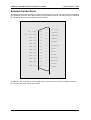
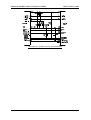
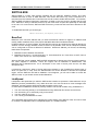
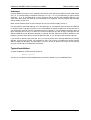
SMT104
Transputer Link Interface
PCMCIA Card
User Manual
SUNDANCE MULTIPROCESSOR TECHNOLOGY LIMITED
SMT104 PCMCIA CARD
Disclaimer
Every effort has been made to ensure the accuracy of the information contained in this
manual, however the manufacturer cannot accept responsibility for any loss or damage
caused as a result of using this document.
Notice of any mistakes, inconsistencies or comments as to ease of use, relating to this
document would be gratefully received in writing or by fax to:
Sundance Multiprocessor Technology Ltd
Fax: +44 (0)1494 793168
IBM and PC DOS are trademarks of International Business Machines Corp.
Transputer, INMOS,T2,T4,T8 and TRAM are trademarks of INMOS Ltd
(c) Sundance Multiprocessor Technology Ltd.
No part of this document may be reproduced in any form or by any means without prior written
permission from S.M.T. Ltd.
Page 2
SUNDANCE MULTIPROCESSOR TECHNOLOGY LIMITED
SMT104 PCMCIA CARD
Index
Introduction......................................................................................................... 4
External Connections......................................................................................... 5
Signal Description .............................................................................................. 6
+LinkOut, -LinkOut......................................................................................................... 6
+LinkIn, -LinkIn .............................................................................................................. 6
+Reset, -Reset ............................................................................................................... 6
+Analyse, -Analyse ........................................................................................................ 6
+Error, -Error.................................................................................................................. 6
5 MHz ............................................................................................................................ 6
LinkSpeed...................................................................................................................... 7
GND............................................................................................................................... 7
VCC ............................................................................................................................... 7
SMT104 I/O Map .................................................................................................. 9
C011 Link Interface............................................................................................. 9
Input Data Register ........................................................................................................ 9
Input Status Register...................................................................................................... 9
Output Data Register.................................................................................................... 10
Output Status Register ................................................................................................. 10
Host System Services ...................................................................................... 11
Reset/Error register ...................................................................................................... 11
Analyse register ........................................................................................................... 11
Interrupts........................................................................................................... 11
Installation of SMT104.EXE Software ............................................................. 12
General........................................................................................................................ 12
PCMCIA Software Overview ........................................................................................ 12
Host PC Configuration.................................................................................................. 12
SMT104.EXE...................................................................................................... 13
BasePort ...................................................................................................................... 13
LinkSpeed.................................................................................................................... 13
Interrupt ....................................................................................................................... 14
Typical Installation ....................................................................................................... 14
Page 3
SUNDANCE MULTIPROCESSOR TECHNOLOGY LIMITED
SMT104 PCMCIA CARD
Introduction
The SMT104 PCMCIA Transputer Link Adapter card contains a single B004 compatible Transputer
interface. This interface is compatible with almost all PC based T2, T4 and T8 Transputer
development tools available in the market today.
The card is designed to connect to a PC via a PCMCIA standard socket. It is housed in a Type II
PCMCIA enclosure, with a single external connector. There are no internal or external user
accessible hardware controls. Any attempt to open the enclosure will render any guarantee void.
The card comes complete with a software configuration utility which can configure the interface to
any desired I/O address, select the link speed, and enable interrupts if desired. This permits the use
of multiple cards to control different Transputer subsystems, or use in PC’s where ports #150 to #163
are not free.
The card is ideally suited for use in notebook computers, many of which now have built in PCMCIA
support. This allows engineers to perform on-site hardware and software development away from the
office without the need for bulky desktop PCs to provide the host for the debugging tools.
The Link interface signals are LinkIn, LinkOut, Reset, Analyse and Error. The LinkOut outputs from
the card are driven by differential line drivers, allowing connection to large Transputer arrays over
long distance with very low data error rates. The LinkIn Inputs to the card are also differential. The
link speed can be programmed to either 10 or 20 Mbit/sec.
Additional outputs are also supplied so that TRAM modules can be driven directly by the SMT104,
without the need for an additional power supply. These outputs include 5Mhz clock, LinkSpeed, and
Ground and +5V power supplies. All you need is a suitable connector to join the SMT104’s D15
connector to the TRAM.
All power for the module is taken from the host PCMCIA slot, so installing the module in a battery
powered portable PC will result in a reduction in battery life. Only +5V power is used , and typical
operating current is around 110mA. The module will not operate at 3.3V.
The PCMCIA standard allows cards to be installed with the PC power switched on (so called Hot
Plugging). You may Hot Plug the SMT104 if necessary. If you are using SMT104.EXE software
driver, the card will automatically configure and deconfigure when the module is installed and
removed. Other, so called 'Non PCMCIA Aware', software may complain if the module is installed or
removed whilst the software is running. The rule of thumb is therefore to install the module before
running any software, and not to remove it before the software terminates.
Page 4
SUNDANCE MULTIPROCESSOR TECHNOLOGY LIMITED
SMT104 PCMCIA CARD
External Connections
All external connections are made via a 25 way breakout lead. One end of the lead has a custom 22
way polarised connector which plugs directly into the PCMCIA module. The other end has a standard
25 way female D connector whose pinout is as follows:
VCC (+5V)
25
Not Connected
24
GND (0V)
23
GND (0V)
22
GND (0V)
21
GND (0V)
20
GND (0V)
19
GND (0V)
18
GND (0V)
17
GND (0V)
16
GND (0V)
15
GND (0V)
14
13
VCC (+5V)
12
-LinkOut
11
+LinkOut
10
-LinkIn
9
+LinkIn
8
LinkSpeed
7
5 Mhz
6
+Error
5
-Error
4
+Analyse
3
-Analyse
2
+Reset
1
-Reset
All GND pins are connected to the 0V supply on the card, and hence to the 0V supply for the host
PC, and also the metal case of the module.
Page 5
SUNDANCE MULTIPROCESSOR TECHNOLOGY LIMITED
SMT104 PCMCIA CARD
Signal Description
+LinkOut, -LinkOut
The +LinkOut and -LinkOut signals are the differential Transputer link outputs from the SMT104. The
signals are driven by a 26LS31 differential line driver chip, which allows reliable connection lengths
of tens of feet. The receiving Transputer system should use 26LS32 (or similar) line receiver chips to
convert the differential signal back to a signal suitable for Transputers.
Alternatively, to connect directly to a TRAM over short distances (up to about a metre) the +LinkOut
signal can be connected directly to any LinkIn on the TRAM. Connecting in this way will result in
much lower immunity to noise on the line, but can be used where a suitable differential receiver is not
available.
+LinkIn, -LinkIn
The +LinkOut and -LinkOut signals are the differential Transputer link inputs to the SMT104
thesignals are received by a 26LS32 differential line receiver chip, which allows reliable connection
lengths of tens of feet. The transmitting Transputer system should use 26LS31 (or similar) line driver
chips to convert the Transputers LinkOut to a differential signal suitable for transmitting to the
SMT104.
Alternatively, to connect directly to a TRAM over short distances (up to about a metre) the +LinkIn
signal can be connected directly to any LinkOut on the TRAM. The -LinkIn signal should be
decoupled to GND using a 100nF capacitor (or similar terminating arrangement) to stop noise on Linkin corrupting the data received on +Linkin. Connecting in this way will result in much lower
immunity to noise on the +Linkin, but can be used where a suitable differential line driver is not
available.
+Reset, -Reset
The +Reset and -Reset signals are differential Reset outputs from the SMT104. The signals are
driven by a 74ACT244 line driver chip, which can source or sink up to 48mA.
To connect directly to a TRAM over short distances, the +Reset signal can be connected directly to
Reset on the TRAM. Connecting in this way will result in lower immunity to noise on the line, but can
be used where a suitable differential receiver is not available.
+Analyse, -Analyse
The +Analyse and -Analyse signals are differential Analyse outputs from the SMT104. The signals
are driven by a 74ACT244 line driver chip, which can source or sink up to 48mA.
To connect directly to a TRAM over short distances, the +Analyse signal can be connected directly to
Analyse on the TRAM. Connecting in this way will result in lower immunity to noise on the line, but
can be used where a suitable differential receiver is not available.
+Error, -Error
The +Error and -Error signals are differential Error inputs to the SMT104. The signals are received by
a 74ACT244 line receiver chip. To prevent the lines from floating, +Error has a 10K pull-down (to
GND) resistor, and -Error has a 10K pull-up (to VCC) resistor.
To connect directly to a TRAM over short distances, the -Error signal can be connected directly to
notError output on the TRAM. Connecting in this way will result in lower immunity to noise on the line,
but can be used where a suitable differential driver is not available.
5 MHz
The 5MHz signal is a 50/50 duty cycle clock output from the SMT104. The signal is driven by a
74ACT244 line driver chip which can source or sink up to 48mA. This output is intended to be used
as the clock input to a TRAM when no other suitable clock is available.
Page 6
SUNDANCE MULTIPROCESSOR TECHNOLOGY LIMITED
SMT104 PCMCIA CARD
LinkSpeed
The LinkSpeed output indicates the current speed setting of the Link on the SMT104. The signal is
driven by a 74ACT244 line driver chip which can source or sink up to 48mA. LinkSpeed is low (0v)
when the link is set to 10Mbit/sec, and High (+5v) when the link is set to 20Mbit/sec. This output is
intended to be used as the LinkSpeedA and/or LinkSpeedB inputs to a TRAM.
GND
The GND are connected to the SMT104 ground voltage, and can be used for signal screening, line
termination or power supply return.
VCC
The two VCC pins can supply +5V to power TRAM’s directly. The output is not fused or current
limited in any way. The amount of current that can be drawn from these pins depends on the host
PC, but as a rule of thumb, should not exceed 1 Amp. Extreme caution should be observed when
using the VCC pins. Under no circumstances should heavy current, short circuits, or other power
supplies be applied to these pins, since permanent damage to the SMT104, the host PC, or both may
result.
750R
110R
110R
750R
100R
750R
750R
OPTIONAL SCREEN
Termination for differential connection
Page 7
SUNDANCE MULTIPROCESSOR TECHNOLOGY LIMITED
SMT104 PCMCIA CARD
Termination for TRAM connection (recommended)
Page 8
SUNDANCE MULTIPROCESSOR TECHNOLOGY LIMITED
SMT104 PCMCIA CARD
SMT104 I/O Map
Once the SMT104 is successfully configured by SMT104.EXE, it responds to I/O access in the same
way as any other B004 compatible interface. A detailed description of the interface is given next.
The SMT104 occupies two I/O port regions, at PortBase to PortBase+#3, and PortBase+#10 to
PortBase+#13. This is compatible with the B004 interface. The first I/O area is used for an IMS C011
link interface chip, whilst the second is used for Host System Services and Interrupt masking. The I/O
map is as follows:
PortBase
PortBase
PortBase
PortBase
+
+
+
+
#0
#1
#2
#3
C011
C011
C011
C011
Input Data register
Output Data register
Input Status register
Output Status register
PortBase
PortBase
PortBase
PortBase
+
+
+
+
#10
#11
#12
#13
Reset/Error register
Analyse register
reserved
Interrupt Enable Register
C011 Link Interface
An IMS C011 link adapter is used as the basis of the link interface on the SMT104. Detailed
information on the device can be found in ‘The Transputer Databook - Third Edition’ from INMOS and
their distributors. This device performs the parallel data to serial INMOS link conversions in both
directions in a fashion similar to a UART device used on a RS232 interface.
The IMS C011 has four registers which can be written to or read by the PC bus. The link adapter
registers function as follows
Input Data Register
The Input Data Register holds the last data byte received from the link. It only contains valid data
while the data present flag is set in the input status register. It cannot be assumed to contain valid
data after it has been read; a double read may or may not return valid data on the second read. It the
data present flag in the input status register is valid on a subsequent read it indicates new data is in
the buffer. Writing to this register has no effect.
Input Status Register
This register contains the data present flag (bit 0, the least significant bit) and the input interrupt
enable control bit (bit 1, the second least significant bit). The data present flag is set to indicate that a
data byte in the input data register is valid. It is reset only when the input data register is read, or by a
link reset condition which will also reset the input interrupt enable control bit.
When writing to this register, the data present flag and the unused bits 2-7 must be written as zero
bits. Note the input interrupt enable bit does not directly control the enabling of interrupts to the PC.
The input interrupt enable bit and the data present bit are anded together to produce a signal called
InputInt. This is used to signal to the interrupt control logic that a valid data byte is present in the link
adapter input data register. The effect of this signal being asserted is dependent on the values written
into the interrupt control register.
Page 9
SUNDANCE MULTIPROCESSOR TECHNOLOGY LIMITED
SMT104 PCMCIA CARD
Output Data Register
Data written to this register is transmitted out of the link. Data must only be written to this register
when the output ready bit in the output status register is set, otherwise data already being transmitted
may be corrupted. Reading this register results in undefined data.
Output Status Register
This register contains the output ready flag (bit 0, the least significant bit) and the output interrupt
enable control bit (bit 1, the second least significant bit). The output ready flag is set to indicate that
the data output buffer is empty. It is reset only when data is written to the output data register; it is set
by a link reset condition which also resets the output interrupt enable control bit.
When writing to this register, the output ready flag and the unused bits 2-7 must be written as zero
bits. Note the output interrupt enable bit does not directly control the enabling of interrupts to the PC.
The output interrupt enable bit and the output ready bit are anded together to produce a signal called
OutputInt. This is used to signal to the interrupt control logic that the output data buffer in the link
adapter is empty. The effect of this signal being asserted is dependent on the values written into the
interrupt control register.
A byte input from the C011 proceeds as follows:
A data byte received on the link is transferred into the input data register and the data present flag in
the input status register is set. If interrupts are enabled, a link data input interrupt is generated. A
processor controlling the PC bus will, either in response to the interrupt or in a polling loop, examine
the input status register. The data present bit will be set signifying valid data in the input data
register.
The processor then reads the data byte. A new data byte can now be received and the process
repeats.
A byte out to the link proceeds as follows:
When the output data register is empty the output ready flag will be set in the output status register. If
interrupts are enabled for this event then an interrupt will be generated. The processor controlling the
PC bus will, either in response to the interrupt or in a polling loop, examine the output status register.
It will determine from the output ready flag that a byte may be written to the data output register. It
then writes a byte to the data output register. The byte is transmitted on the Link output. When the
link adapter is next able to transmit a butte the output ready flag will be set again.
Page 10
SUNDANCE MULTIPROCESSOR TECHNOLOGY LIMITED
SMT104 PCMCIA CARD
Host System Services
Two ports are used to reset and analyse the Transputer(s) connected to the SMT104. A detailed
description of these ports is given next.
Reset/Error register
Bit 0 of this register controls the state of the +Reset and -Reset signals. Writing a one to this bit
resets the IMS C011 chip on the SMT104, sets +Reset high, and -Reset low, causing a reset on
connected Transputers. Writing a 0 to this bit clears the reset from the IMS C011, sets +Reset low
and -Reset high. Note that this bit must be set high for a minimum of 100mS. Writing to bits 1-7 of
this register has no effect.
Reading from this register returns the state of the +Error/-Error differential input in bit 0. This bit is
zero when +Error is high or when -Error is low (showing that an error has occurred). Bits 1 to 7 of this
register are undefined when read.
Analyse register
Bit 0 of this register controls the state of the +Analyse and -Analyse signals. Writing a one to this bit
sets +Analyse high, and -Analyse low. Writing a 0 sets +Analyse low and -Analyse high. Analyse is
used in conjunction with Reset, to stop a Transputer connected to these signals. It allows the internal
state of the Transputer to be examined so that the cause of an error may be determined. A processor
in analyse mode can be interrogated on any of its links.
Writing to bits 1-7 of this register has no effect. A read from this register will result in undefined data
being read.
Interrupts
The SMT104 has additional features not normally found on B004 compatible hardware. It can
generate an interrupt on the PC bus when one of the following events occurs:
•
•
•
+Error is asserted (set to +5V) or -Error is asserted (set to 0V)
The OutputInt signal from the IMS C011 is asserted
The InputInt signal from the IMS C011 is asserted
The generation of these interrupts is compatible with the B008 standard, and is controlled by three
bits in the interrupt enable register. Bits 1-3 are used to mask (disable) or enable interrupts for each
event. Setting a bit to one in the register enables interrupts on the event corresponding to that bit.
The bits are defined as follows:
Bit 1
Bit 2
Bit 3
Error Interrupt enable
Link output interrupt enable (OutputInt asserted)
Link input interrupt enable (InputInt asserted)
Data written to bits 0 and 4-7 has no effect. A read from this register will result in undefined data
being read.
The interrupt channel used by the SMT104 to request an interrupt is entered as a command line
argument when installing SMT104.EXE. If no interrupt channel is requested when installing SMT104,
then the setting of the bits in this register will have no effect, and no interrupts will be generated.
Bits 1 to 3 of this register are cleared to zero when the SMT104 is first initialised, thus masking off all
interrupts until they are specifically enabled by the users software. It is the responsibility of the users
software to ensure that a valid interrupt service routine is installed before any interrupts are enabled.
Failing to do this may result in a system crash due to unexpected interrupts.
Page 11
SUNDANCE MULTIPROCESSOR TECHNOLOGY LIMITED
SMT104 PCMCIA CARD
Installation of SMT104.EXE Software
General
The Personal Computer Memory Card International Association (PCMCIA) has defined several
standards for hardware and software to allow the easy interchange of Personal Computer Interface
Cards (PC Cards). The SMT104 PCMCIA module conforms to release 2.10 of these standards.
Many 'notebook' PC's now come equipped with one or more PCMCIA compatible interface slots. The
SMT104 PCMCIA module should work on any such computer which has at least one Type II release
2.1 compliant socket.
PCMCIA Software Overview
The software interface between the PCMCIA hardware and the PC is performed by layers of software
which are usually supplied with the PC.
The lowest layer is called 'Socket Services', and this provides all the interface software required to
interface to the socket adapter chip fitted in the Host PC. Socket Services is sometimes part of the
PC's BIOS, but more often is loaded as a device driver in your CONFIG.SYS.
The next software layer is called 'Card Services', and this provides a common software interface
between user applications and Socket Services. Card Services is responsible for keeping track of
resources (Memory, I/O and Interrupts) which are allocated to PCMCIA cards, and is usually loaded
as a device driver in your CONFIG.SYS.
Both Socket Services and Card Services are supplied with the PC. If you do not have either of these,
you must obtain copies from your PC's manufacturer or distributor. SUNDANCE cannot supply these
programs because they are machine dependent, and usually copyrighted.
Host PC Configuration
The host PC must have Socket Services and Card Services installed to use PCMCIA cards. These
will typically be installed as part of your CONFIG.SYS as :
DEVICE=SS.EXE
DEVICE=CS.EXE
Other PCMCIA drivers may also be loaded afterwards.
The configuration utility SMT104.EXE, with required parameters, should also be installed in your
AUTOEXEC.BAT file. This program will automatically recognise when an SMT104 card is inserted
as described above. SMT104.EXE will report an error if Socket Services or Card Services are not
installed when it is run.
Page 12
SUNDANCE MULTIPROCESSOR TECHNOLOGY LIMITED
SMT104 PCMCIA CARD
SMT104.EXE
SMT104.EXE is a DOS TSR program supplied with the SMT104 PCMCIA module, and when
installed becomes a client of Card Services. This means that when any card is inserted into or
removed from the PCMCIA slot, Card Services will call routines inside SMT104.EXE. On insertion,
SMT104.EXE will inspect information contained in a ROM on the card, and if it decides that the card
is an SMT104, it will try to allocate resources (in this case some I/O ports and optionally an Interrupt)
to the card. On card removal, SMT104.EXE will free any resources that have been allocated to the
card.
To install SMT104.EXE you should type :
SMT104 BasePort,LinkSpeed,Interrupt
BasePort
BasePort is the I/O base address that you wish the SMT104 interface to appear at. INMOS cards
usually reside at address #150, with jumper selectable alternatives at #200 and #300.
PCMCIA cards do not have jumpers, and the SMT104 card can be configured to reside at almost any
address. You are strongly advised to stick to #150 if at all possible, since not all Transputer software
can be configured to work at a different I/O address. Whichever address you choose, the following
restrictions are imposed :
1. BasePort must be between 0 and #3F0.
2. BasePort must be on a 16 port boundary. i.e. #150,#160,#170 etc. Ports #151 to #15F, #161 to
#16F, #171 to #17F etc. are not permitted.
When a SMT104 card is installed, SMT104.EXE will attempt to allocate two I/O port regions based on
the value supplied in BasePort. These two regions will be BasePort to BasePort+#3, and
BasePort+#10 to BasePort+#13. For a description of the uses of these ports see the I/O Map
description later.
It should be noted that if either of these regions are already in use (CardServices keeps track of
which I/O ports are in use), then the SMT104.EXE will not be allowed to allocate the requested
region, and the SMT104 card will be disabled. If this happens, you will not be able to access the
SMT104 card, so you should choose another BasePort.
LinkSpeed
LinkSpeed is the speed that you wish the SMT104 link interface to operate at. Valid values are 10 (10
Mbits/sec) and 20 (20 Mbits/sec). Any value other than 10 or 20 will cause an error message to be
displayed, and the program will terminate without setting up the card.
In most cases 20 Mbits/sec should be perfectly reliable. You should consider using 10 Mbits/sec if :
1.
2.
3.
4.
You are connecting directly to a TRAM without using differential line drivers and receivers.
You are working in an electrically noisy environment .
Your link cable is very long.
You cannot get 20 Mbits/sec to work !
The LinkSpeed output will be set to indicate the current setting of the SMT104 card, and can be used
to control the LinkSpeedA and/or LinkSpeedB inputs on a TRAM if desired.
Page 13
SUNDANCE MULTIPROCESSOR TECHNOLOGY LIMITED
SMT104 PCMCIA CARD
Interrupt
Interrupt determines which, if any, hardware interrupt is to be used by the SMT104 card. Valid values
are 1 to 15 (corresponding to hardware interrupts 1 to 15), ‘n’ or ‘N’ (corresponding to (N)o Interrupt
required) , ‘a’ or ‘A’ (corresponding to (A)ny Interrupt, that is use the first available Interrupt). Any
value other than these will cause an error message to be displayed, and the program will terminate
without setting up the card.
Most current software does not use interrupts, and so you would normally choose ‘n’.
It should also be noted that although a PC has provision for 15 interrupts, most of them are reserved
for system usage. Typically only three or four are available for interface cards such as the SMT104. If
you request an interrupt, and the requested interrupt is already in use (CardServices keeps track of
which Interrupts are in use), or if there are no free interrupts (in the case of (A)ny Interrupt) then the
SMT104.EXE will not be allowed to allocate an interrupt, and the SMT104 card will be disabled. If this
happens, you will not be able to access the SMT104 card, so you should choose another Interrupt.
If you chose to allocate (A)ny Interrupt, then you cannot predict which interrupt SMT104 will actually
allocate. You will need to write your software so that it can inquire of CardServices which interrupt
SMT104.EXE has allocated. The description of how to do this is beyond the scope of this manual,
and you should refer to PCMCIA documentation.
Typical Installation
A typical installation of SMT104.EXE would be:
SMT104 150,20,n
This line (or one with the desired parameters) should be inserted in your AUTOEXEC.BAT .
Page 14