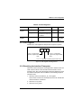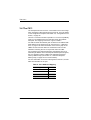
1
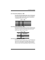
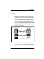
TMB15 User Manual Ref: 15 M 711 Document reference number 15 M 711. Copyright 1997 Transtech Parallel Systems. This publication is protected by Copyright Law, with all rights reserved. No part of this publication may be reproduced, stored in a retrieval system, translated, transcribed, or transmitted, in any form, or by any means manual, electric, electronic, mechanical, chemical, optical or otherwise, without prior written permission from Transtech Parallel Systems. Transtech reserves the right to alter specifications without notice, in line with its policy of continuous development. Transtech cannot accept responsibility to any third party for loss or damage arising out of the use of this information. Transtech acknowledges all registered trademarks. Transtech Parallel Systems Corp 20 Thornwood Drive Ithaca NY 14850-1263 USA Transtech Parallel Systems Ltd 17-19 Manor Court Yard Hughenden Avenue High Wycombe Bucks, HP13 5RE United Kingdom tel: 607 257 6502 fax: 607 257 3980 tel: +44 (0) 1494 464303 fax: +44 (0) 1494 463686 [email protected] http://www.transtech.com [email protected] http://www.transtech.co.uk Table of Contents Chapter 1 About this manual 1 Chapter 2 Installation 3 2.1 Before You Start ...................................................................... 3 2.2 Configuration ........................................................................... 4 2.2.1 Switches ........................................................................ 4 2.2.2 VME Board Address ...................................................... 5 2.3 Installing the TMB15 ............................................................... 6 2.4 Software .................................................................................. 6 Chapter 3 The TMB15 7 3.1 Overview ................................................................................. 8 3.2 Hardware Description ............................................................ 10 3.2.1 Front Panel Switches: SW1 ......................................... 11 3.2.2 Front Panel Switches: SW2 ......................................... 11 3.2.3 Front Panel Switches: SW3 ......................................... 11 3.2.4 SW4 Switch Bank ........................................................ 12 3.2.5 VME Address Switches ............................................... 14 3.3 TMB15 Control Registers ...................................................... 15 3.3.1 LED Register ............................................................... 17 3.3.2 Resetting the Interface Transputer .............................. 17 3.4 The C011 .............................................................................. 18 3.5 VME Interface ....................................................................... 19 3.5.1 VME A32 Mode ........................................................... 20 3.5.2 VME A24 Mode ........................................................... 21 3.6 Interface Transputer Memory Map ........................................ 22 3.7 Flash ROM ............................................................................ 23 3.8 Link Architecture ................................................................... 23 3.9 Configuration Architecture ..................................................... 28 3.10 System Services Architecture ............................................. 29 3.11 Interrupts ............................................................................. 30 15 M 711 TMB15 User Manual i 3.12 Edge Connector Pinout Details ............................................31 Chapter 4 Solaris 2 Software Installation 37 4.1 FORCE CPU-3CE .................................................................37 4.2 FORCE CPU-5V ....................................................................38 4.3 Installation ..............................................................................38 4.4 Before Continuing ..................................................................39 4.5 Configuration File ...................................................................39 4.6 Confidence Test .....................................................................42 4.7 Environment Variables ...........................................................42 Chapter 5 Support Software 45 5.1 Device Driver .........................................................................45 5.2 TMB15 Firmware ...................................................................47 5.3 TMB15 Examples ..................................................................48 5.3.1 MMS .............................................................................48 5.3.2 c004rst .........................................................................48 5.3.3 flashtst ..........................................................................48 5.4 check and iserver ...................................................................49 5.5 Aserver ..................................................................................49 5.6 bootvme .................................................................................49 Chapter 6 Programming the TMB15 51 6.1 Booting the Interface Transputer ...........................................51 6.1.1 Boot from Link ..............................................................52 6.1.2 Boot from Flash ............................................................52 6.1.3 Boot from VME .............................................................53 6.2 LED Example .........................................................................53 Index ii TMB15 User Manual 55 15 M 711 Chapter 1 About this manual This manual describes the Transtech TMB15 VME transputer module (TRAM) motherboard. • “Installation” on page 3 gives an overview of the process of installing a TMB15. • “The TMB15” on page 7 gives a full description of the TMB15 hardware and a reference to all of the user configurable switches and jumpers on the board. • “Solaris 2 Software Installation” on page 37 describes the process of installing the Solaris 2 software support for the TMB15. • “Support Software” on page 45 details the supplied software support for the TMB15. • “Programming the TMB15” on page 51 describes how the TMB15’s interface Transputer can be programmed with user’s application code. Please refer to the Transtech Transputer Motherboard User Manual for general information on using TRAM modules and TRAM motherboards. 15 M 711 TMB15 User Manual 1 About this manual 2 TMB15 User Manual 15 M 711 Before You Start Chapter 2 Installation CAUTION - STATIC SENSITIVE DEVICES The TMB15 uses CMOS devices which can be permanently damaged by static discharge. Please observe the following precautions when handling the board: • Always transport the board in an antistatic box or bag. • Don’t touch any of the components on the board. • It is recommended that you wear an earthed wrist strap when handling the board. If one is not available, it is recommended that you ground yourself on a metal part of the casing of your VME rack, which will be earthed, before touching any part of the board. The switches and jumpers referred to in this section can be located on the TMB15 with the aid of figure 4, “TMB15 Board Layout,” on page 10. All switches and jumpers are also clearly marked on the TMB15 motherboard itself. Full details of switch settings can be found in section 3.2, “Hardware Description,” on page 10. 2.1 Before You Start Before installing the TMB15 hardware or software, please read this section carefully. It is recommended that you install the VME controller hardware and software before installing the TMB15. If you wish to use a FORCE CPU-3CE board running Solaris2 to control a TMB15, please follow the instructions in section 4.1, “FORCE CPU-3CE,” on page 37. If you intend to use a TMB15 as a hostlink interface (i.e. to run iserver, check or Inquest using the TMB15 as an interface 15 M 711 TMB15 User Manual 3 Configuration between a host and the processor network) then you should install the device driver software for that board. If you intend to run your own application code on the TMB15’s interface Transputer then you should not install the device driver software for that board. You will need another hostlink interface such as a TMB14 or another TMB15 to able to use Inquest (for example) to debug code running on the TMB15’s host interface. 2.2 Configuration 2.2.1 Switches When using a TMB15 as a hostlink interface, the interface Transputer runs code programmed into its flash memory. Thus you should set the front panel switches to the following: • Config C011 (SW1 UP). • Boot from ROM (SW2 DOWN). • Boot from Flash (SW3 UP). These switch settings are shown in figure1: SW1 SW2 SW3 Figure 1. Default Front Panel Switch Settings The following settings should be used for the on-board switches: 4 • Use flat mode (SW4.2 OFF) unless TRAM slots 1 to 7 are to be reset using TRAM 0’s subsystem pins. • Enable lock on boot when booting from Flash ROM or VME (SW4.3 OFF, SW4.4 ON). TMB15 User Manual 15 M 711 Configuration • 20 MB/s links (SW4.5 OFF) unless 10 MB/s links are required (SW4.5 ON). • Config to the front panel connector J1 (SW4.6 ON) or to P2 (SW4.6 OFF) as required. • Disable VME power on reset (SW4.7 OFF). • Enable the VME interface (SW4.8 OFF). The default switch settings are shown in figure 2 ON 1 2 3 4 5 6 7 8 Figure 2. Default SW4 Settings See 3.2, “Hardware Description,” on page 10 for details of the front panel and on-board switches. 2.2.2 VME Board Address You need to choose a suitable board address for each TMB15 installed into a VME rack. In A32 mode the TMB15 decodes a 16MB region of VME address space. In A24 mode the region is 4MB. See figure 5, “VME Address Switches,” on page 14 for details of how to set the VME board address. If the TMB15 is to be used in A32 mode, set the top two rotary switches to the eight most significant VME base address bits. A value of 0x08 corresponding to a base address of 0x08000000 is often suitable. Set the bottom rotary switch to 0xF. On the FORCE 3CE, the value 0x00000000 is normally not available as this would clash with the default base address of the 3CE’s VME slave memory. If the TMB15 is to be used in A24 mode, the settings of the top two rotary switches are ignored. Set the bottom rotary switch to a value of 0x0, 0x1, 0x2 or 0x3 to set the two most significant bits of the VME base address (i.e. addresses 0x000000, 0x400000, 0x800000 or 0xc00000). A value of 0x1 corresponding to a base address of 0x400000 is often suitable. On the FORCE 3CE, the 15 M 711 TMB15 User Manual 5 Installing the TMB15 value 0x3 is not available as the last 64K of A24 address space is reserved for A16 mode. 2.3 Installing the TMB15 After configuring the TMB15 hardware, proceed with the following steps to install the TMB15 hardware: 1. If you have not done so already, install any required transputer modules onto the TMB15. 2. Remove the power to the VME rack. 3. Plug the board in and bolt it down. 4. Switch on the VME rack. 2.4 Software Details of how to install the Solaris 2 software for the TMB15 are given in Chapter 4. 6 TMB15 User Manual 15 M 711 Software Chapter 3 The TMB15 This chapter describes the TMB15 hardware. The summary below provides a “roadmap” of the sections contained in this chapter to assist quickly locating any reference information needed. 15 M 711 • Section 3.1, “Overview,” on page 8 gives an overall description of the TMB15s features and contains a block diagram of the board’s architecture. • Section 3.2, “Hardware Description,” on page 10 gives a complete description of all user configurable switches on the TMB15. • Section 3.3, “TMB15 Control Registers,” on page 15 describes the board control registers. • Section 3.4, “The C011,” on page 18 describes the C011 on the TMB15. • Section 3.5, “VME Interface,” on page 19 describes the VME interface. It includes address maps of the TMB15 as seen from the VME bus. • Section 3.6, “Interface Transputer Memory Map,” on page 22 shows the interface transputer memory map. • Section 3.7, “Flash ROM,” on page 23 describes the 128K of Flash ROM fitted on the TMB15. • Section 3.8, “Link Architecture,” on page 23 describes the architecture of the electronic transputer link switches on the TMB15. • Section 3.9, “Configuration Architecture,” on page 28 describes the connectivity of the configuration T225 processor (the processor which sets the electronic link switches). TMB15 User Manual 7 Overview • Section 3.10, “System Services Architecture,” on page 29 describes the options for configuring the TRAM subsystem architecture of the TMB15. • Section 3.11, “Interrupts,” on page 30 describes the facilities provided for TMB15 to VME and VME to TMB15 interrupts. • Section 3.12, “Edge Connector Pinout Details,” on page 31 gives detailed pin number information for all the external connectors provided on the TMB15. For a general introduction to TRAM modules and motherboards please refer to the Transtech Transputer Motherboard User Manual. 3.1 Overview The TMB15 is a combined 8 slot TRAM motherboard and a high performance transputer VME slave. The TMB15 specification is summarized as follows: 8 • 6U by 160mm VME format board. • T805 or T425 interface transputer with 4MBytes of fast EDRAM memory shared with the VME bus. • 8 TRAM sites with all links connected to a pair of socketed C004 link crossbars for electronic reconfiguration of the link topology. • Highly optimized 32bit slave VME interface. • A24/A32 VME addressing and D32/D16/D08(EO) data transfer support. • Flexible byte/word swapping memory regions for endian conversion. • C011 interfaced to both the VME bus and the interface transputer for configuring the C004 switches (via a T225 transputer). • Front panel connections (J1/J2) for transputer links and subsystem signals. • P2 connections for transputer links and subsystem signals. • 3 user programmable LEDs and an Error LED mounted on the front panel. • Interface transputer boot from flash ROM or shared memory option. • No components are fitted to the top surface of the board within the TRAM sites. TMB15 User Manual 15 M 711 Overview The VME interface is a highly optimized 32bit slave interface. VME bus writes are posted to give maximum transfer performance from a bus master. The interface also recognizes sequential VME reads from the EDRAM memory and prefetches data whenever possible. A block diagram of the TMB15 is shown in figure 3. VME bus VME Bus Interface 4MBytes EDRAM Flash ROM Interface transputer TRAM slots Control registers C011 ConfigUP T225 C004 Text P2 J1/J2 ConfigDOWN Figure 3. TMB15 Block Diagram 15 M 711 TMB15 User Manual 9 Hardware Description 3.2 Hardware Description The TMB15 board layout is shown in figure 4. SW1 TRAM 3 SW2 SW3 ON 1 TRAM 7 P1 SW4 LED0 LED1 LED2 Error TRAM 4 8 TRAM 0 A0 A1 J1 TRAM 2 A2 TRAM 6 J2 TRAM 5 P2 TRAM 1 Figure 4. TMB15 Board Layout 10 TMB15 User Manual 15 M 711 Hardware Description 3.2.1 Front Panel Switches: SW1 SW1 determines the ConfigUP link taken to the configuration T225 processor. The choices to select from are: the C011, J1 ConfigUP or P2 ConfigUP. Details are given in table 1. For more information on controlling the TMB15 configuration architecture, see section 3.9, “Configuration Architecture,” on page 28. Table 1: SW1 SW1 SW4.6 ConfigUP UP any C011 DOWN ON J1 ConfigUP DOWN OFF P2 ConfigUP 3.2.2 Front Panel Switches: SW2 SW2 determines whether the interface transputer will attempt to boot from memory or from link. When the switch is set to boot the interface transputer from memory, the actual memory bank used is determined by SW3. Details are given in table 2. Table 2: SW2 SW2 Interface transputer boots from: UP Link DOWN Memory (as determined by SW3) 3.2.3 Front Panel Switches: SW3 SW3 determines the memory bank that the interface transputer will boot from when it is set to “boot from memory mode”. The choices to select from are either EDRAM or Flash ROM. Details are given in table 3. For more information on setting the interface transputer to boot from memory mode, see the description of SW2. For more infor- 15 M 711 TMB15 User Manual 11 Hardware Description mation on the effect of this switch on the interface transputer, see section 3.6, “Interface Transputer Memory Map,” on page 22. Table 3: SW3 SW3 Interface transputer boots from: UP Flash ROM DOWN EDRAM 3.2.4 SW4 Switch Bank SW4 determines a number of miscellaneous board configuration options. Details are given in table 4. Switches 4.3 and 4.4 determine whether VME or Transputer lock is asserted when the interface Transputer is booting. When booting from Flash memory, the interface Transputer must have exclusive access to its memory and registers, thus Transputer lock is asserted after reset. When booting from EDRAM memory, VME lock must be asserted after reset so that a program can be written into memory and then executed by the interface Transputer by removing VME lock. When booting from link no locking of the bus is required. The two switches allow complete control over this function, i.e. always on, always off or controlled by SW2. The third option is recommended SW4.3 OFF, SW4.4 ON. Switch 4.5 controls the link speeds of all links on the interface transputer and all links on all transputers mounted on the TRAMs in the TRAM sites. Switch SW4.7 enables the TMB15 to drive the VMEreset whenever the board is powered on. Note that some VME systems do not assert VMEreset for sufficiently long to reset all the components on the TMB15 when the system is powered on. In such systems, you should set the switch to OFF to allow the TMB15 to hold VMEreset active whilst it runs through its power on cycle. If you are sure that the VMEreset is active after power on for long enough to reset all the components on the TMB15, then its is safe to set SW4.7 to ON. 12 TMB15 User Manual 15 M 711 Hardware Description Table 4: SW4 Switch Setting 4.2 ON 4.2 OFF Action More information TRAMs 1 to 7 subsystem services Section 3.10, “Systaken from TRAM 0’s subsystem port tem Services Architecture,” on TRAMs 1 to 7 subsystem services page 29. taken from the same source fed to TRAM 0 4.3 ON Never set VME or Transputer lock on reset, regardless of SW4.4 position. 4.3 OFF Set VME or Transputer lock on reset depending on SW3, BUT see SW4.4 4.4 ON VME or Transputer Lock on reset is set whenever SW2 is DOWN. SW4.3 must be OFF 4.4 OFF SW4.3 has complete control over VME and Transputer Lock on reset. 4.5 ON Transputer link speed set to 10Mbits/sec 4.5 OFF Transputer link speed set to 20Mbits/sec. 4.6 ON ConfigDOWN taken to J1. ConfigUP taken from J1 according to SW1 4.6 OFF ConfigDOWN taken to P2. ConfigUP taken from P1 according to SW1 4.7 ON Do not drive VMEreset on power up 4.7 OFF Drive VMEreset on power up 4.8 ON Disable the VME interface 4.8 OFF Enable the VME interface 15 M 711 See notes above. See notes above. See notes above. Section 3.9, “Configuration Architecture,” on page 28 See notes above. TMB15 User Manual 13 Hardware Description 3.2.5 VME Address Switches The VME address switches A0, A1 and A2 determine both the TMB15 VME address and whether the board is in A24 address mode or A32 address mode. Switches A0 and A1 select the top 8bits of the board’s A32 mode address. In A32 mode the TMB15 occupies 16MBytes of the VME memory map. Switches A0 and A1 select one of the 256 possible such 16MByte aligned blocks the board could occupy. Switch A2 selects the top 2 bits of the board’s A24 mode address. In A24 mode the TMB15 occupies 4MBytes of the VME address map. Switch A2 selects which of the 4 possible such 4MByte aligned blocks the board could occupy. Details are given in figure 5. A0 EF 0 1 2 D 3 C 4 B 5 A 9876 Top 4 address bits (VA28..VA31) of A32 mode addresses. A1 EF 0 1 2 D 3 C 4 B 5 A 9876 Second most significant nibble address bits (VA24..VA27) of A32 mode addresses. A2 EF 0 1 2 D 3 C 4 B 5 A 9876 Top 2 address bits (VA22..VA23) of A24 mode addresses. Only the values 0, 1, 2 and 3 are valid for A24 mode addressing. Set the switch to F to select A32 mode addressing. Figure 5. VME Address Switches 14 TMB15 User Manual 15 M 711 TMB15 Control Registers 3.3 TMB15 Control Registers The TMB15 control registers are accessible both by the VME bus and by the interface transputer. A description of all of the control registers is given in table 5. For each register, the table shows: • Group. Registers with related functionality are assigned to groups. Elsewhere in this manual, a reference to a register group should be taken as a reference to all the registers in that register group. • Register Name. • Register Function. A brief description of what the register is used for. Sometimes this will be a reference to another section in the manual which discusses that area of functionality in greater detail. • Address. For VME accesses the address given is relative to the TMB15 VME base address set by switches A0-A2. See section 3.5, “VME Interface,” on page 19 for more information on the memory map of the TMB15 as seen from the VME bus. The registers are accessed as the least significant byte in each word, thus add 3 to the offset address if byte-wide accesses are made to the registers from VME. For accesses by the interface transputer, the address given is the absolute byte address of the register. Since the transputer address space is signed, the control registers appear in the middle of the interface transputer’s memory address map (see section 3.6, “Interface Transputer Memory Map,” on page 22 for more information). • Bits. Only the bits specified in this column are valid. When writing to a register set all other bits to 0. When reading from a register, mask all other bits. Registers are either write-only, read-only or read-write, designated in the table by (W), (R) and (RW) respectively. For single bit registers, writing the register bit to the value 1 corresponds to asserting the signal associated with the register. Writing the register bit to 0 corresponds to de-asserting the signal associated with the register. Similarly, reading the register bit as a 1 implies that the signal associated with the register is asserted. 15 M 711 TMB15 User Manual 15 TMB15 Control Registers Table 5: Control Registers Group TRAM subsystem registers Register Name Register Function Address Possible source of TRAM subsystem services. See section 3.10, “System Services Architecture,” on page 29 for details. 00 D0 (W) 00 D0 (R) 04 DO (W) 10 D0 (W) 14 D0 (W) Tif_Error Possible source of interface transputer subsystem services. See section 3.10, “System Services Architecture,” on page 29 for details. 18 D0 (R) LED Front panel LEDs 1C D0-D2 (W) Tif_Lock Lock memory and registers for the exclusive use of the Interface Transputer 20 D1 (RW) VME_Lock Lock memory and registers for the exclusive use of the VME interface. 24 D1 (RW) PAGE A24 addressing mode page register. See section 3.5, “VME Interface,” on page 19 for more details 28 D0-D1 (RW) Generates an interrupt to the interface transputer 30 D2 (RW) Int_VME Generates an interrupt to the VME bus 34 D1 (RW) VME_IRQ_Level VME interrupt level 1-7. Set to zero to disable VME interrupts 38 D0-D2 (RW) C011_Int Directs C011 interrupts to the interface transputer (asserted) or the VME bus (not asserted) 40 D2 (RW) Int_Acknowledge Acknowledges the Transputer interrupt enabling an event on the next interrupt 44 Any (W) 4C Any (W) Tram_Reset Tram_Error Tram_Analyse Interface transputer registers Bus locking registers Tif_Reset Tif_Analyse Interrupt control Int_Tif registers Remove_Tif_Lock VME writing any value to this register forces the removal of the Interface Transputer’s bus lock 16 TMB15 User Manual Bits 15 M 711 TMB15 Control Registers Table 5: Control Registers Group Flash ROM registers Register Name Register Function Address Flash_Program Sets Flash ROM programming voltage 50 D1 (W) Flash_Bits Sets the two least significant bits of the Flash memory address 54 D0-D1 (W) VME interrupt vector number 60 D0-D7 (RW VME Only) Interrupt control VME_IRQ_Vector registers Bits 3.3.1 LED Register Details of the LED register bit assignments are given in figure 6 D2 set to ‘1’ to light LED2 (bottom programmable LED) D1 D0 set to ‘1’ to light LED0 (uppermost programmable LED) set to ‘1’ to light LED1 (middle programmable LED) Figure 6. LED Register bit assignments 3.3.2 Resetting the Interface Transputer When the interface transputer reset register bit is asserted, the next VME access must be a write and will cause the reset to be deasserted. Thus, when using the interface transputer registers to reset the interface transputer from the VME bus, the following sequence should be used: 1. Write any value to the Remove_Tif_Lock register. This forces the removal of the transputer’s bus lock and will also clear the reset if it is asserted. 2. Write one to Tif_Reset. 3. Write zero to Tif_Reset. 15 M 711 TMB15 User Manual 17 The C011 3.4 The C011 The transputer link from the C011 can be taken to the T225 configuration transputer to allow the link topology to be set. For more details on the configuration transputer see section 3.9, “Configuration Architecture,” on page 28. The C011 is used in its mode2 of operation i.e. in C012 compatibility mode. It is accessible both by the VME bus and by the interface transputer. The mapping of the C011 is given in table 6. For VME accesses the address given is relative to the TMB15 VME base address set by switches A0-A2. See section 3.5, “VME Interface,” on page 19 for more information on the memory map of the TMB15 as seen from the VME bus. Remember to add 3 to this address if accessing the C011 in byte-wide mode over VME. For accesses by the interface transputer, the address given is an absolute byte address. Since the transputer address space is signed, the C011 appears near the middle of the interface transputer’s memory address map (see section 3.6, “Interface Transputer Memory Map,” on page 22 for more information). For more information on the use of the registers in the C011, see the SGS documentation for the part. Table 6: C011 Address Mapping Register 18 TMB15 User Manual Address Read data 70 Write data 74 Input status 78 Output status 7C 15 M 711 VME Interface 3.5 VME Interface All of the EDRAM and all the control registers are accessible from the VME bus. The TMB15 supports A32 D32, A32 D16 and A32 D08(EO) accesses, and A24 D32, A24 D16 and A24 D08 (EO) accesses. It does not support A16 accesses. Unaligned cycles are not supported. To provide the required endian conversion between the VME and transputer data buses the EDRAM is mapped to the VME bus three times. Once with the same byte ordering as seen by the transputer, once with consecutive pairs of 16bit words swapped and once with groups of 4 bytes swapped. This provides the system designer with the option of accessing 16 bit data streams and 8 bit data streams with 32 bit access cycles and have any necessary byte/word swapping handled in hardware. Details of the byte swapping behavior of the TMB15 are shown in figure 7. Data seen by interface transputer D31 D23 D15 D7 D24 D16 D8 D0 D31 D15 D16 D0 D31 D0 Data seen by VME bus master byte swapping 16 bit word swapping No swapping D31 D23 D15 D7 D24 D16 D8 D0 D31 D15 D16 D0 D31 D0 Figure 7. TMB15 Byte Swapping Behavior In circumstances where both the VME bus and the interface transputer are competing for access to the EDRAM, arbitration is performed on a rotating basis for each such access. This guarantees 15 M 711 TMB15 User Manual 19 VME Interface that neither the VME bus nor the interface transputer can lock the other out of the EDRAM for more than one memory cycle. 3.5.1 VME A32 Mode In A32 address mode the TMB15’s VME base address is set by address switches A0, A1 and A2. See section 3.2.5, “VME Address Switches,” on page 14 for details of these switches. The 16MByte VME bus address map for the TMB15 A32 address mode is shown in figure 8. Memory Address EDRAM image (no swapping) board base + 0xC00000 EDRAM image (16bit word swapped) board base + 0x800000 EDRAM image (byte swapped) board base + 0x400000 Control registers board base + 0x000000 Figure 8. TMB15 VME Address Map (A32 addressing) 20 TMB15 User Manual 15 M 711 VME Interface 3.5.2 VME A24 Mode In A24 address mode the TMB15’s VME base address is set by address switch A2. See section 3.2.5, “VME Address Switches,” on page 14 for details of this switch.The 4MByte VME bus address map for the TMB15 A32 address mode is shown in figure 9. Memory Address paged EDRAM image (no swapping) board base + 0x300000 paged EDRAM image (16bit word swapped) board base + 0x200000 paged EDRAM image (byte swapped) board base + 0x100000 Control registers board base + 0x000000 Figure 9. TMB15 VME Address Map (A24 addressing) In order to minimize address space occupancy of the TMB15 in A24 address mode, the EDRAM is mapped in 1MByte windows onto the VME bus. Control of which of the 4 possible such windows mapped to the VME bus is set by the PAGE control register, as shown in table 7. Table 7: PAGE Register Settings PAGE Register Value 15 M 711 EDRAM mapped to VME interface 0 0x000000 - 0x0FFFFF 1 0x100000 - 0x1FFFFF 2 0x200000 - 0x2FFFFF 3 0x300000 - 0x3FFFFF TMB15 User Manual 21 Interface Transputer Memory Map 3.6 Interface Transputer Memory Map The TMB15 memory map from the perspective of the interface transputer is given in figure 10. Memory Address 0x7FFFFFFF Boot memory See description below Control registers 0x00000000 0xC0020000 Flash ROM 0xC0000000 0x80401000 EDRAM Internal memory 0x80001000 0x80000000 Figure 10. Interface Transputer Memory Map The boot memory can be either a second mapping of the EDRAM memory or a second mapping of the Flash ROM memory, according to the setting of SW3 (see section 3.2.2, “Front Panel Switches: SW2,” on page 11 for the actual switch settings). Note that whether the interface transputer actually attempts to boot from the boot memory depends on the setting of SW2. When the interface transputer is booting from boot memory, the top of memory should contain a backwards jump instruction to the beginning of the main program. 22 TMB15 User Manual 15 M 711 Flash ROM 3.7 Flash ROM The TMB15 has 128K of Flash ROM fitted. The interface Transputer can load and run a program from this Flash ROM if required. This is how the firmware for the SunOS device driver is run after a reset. The Flash memory can be accessed from the interface Transputer only. It cannot be accessed from VME. Furthermore, VME accesses to any part of the TMB15’s memory map must be disabled when accesses are made to the Flash ROM. Thus the interface transputer bus lock must be asserted either by explicitly writing to the relevant register or automatically after a reset when boot from Flash is selected. When the transputer lock signal is asserted and the boot from Flash switch is set, the Flash ROM appears in the interface transputer’s memory in two places. In the 128K region up to address 0x7fffffff the Flash ROM appears to be 32 bits wide and is read only. This is the place at which the transputer starts executing in boot from ROM mode. In the 128K region starting at address 0xc0000000, the least significant byte of each word accesses one byte of the flash ROM and can be read or written. The actual byte accessed in the word is selected by the contents of the Flash memory LSBs register. This is the region in which Flash memory programming is performed. The method by which the Flash memory can be programmed is not documented here. Please refer to the manufacturer’s documentation for details. The source code of a programming utility flashtst.c is supplied which runs on the interface transputer and can be used either to test or to program the Flash memory. 3.8 Link Architecture The TMB15 uses two C004 (C004a and C004b) link crossbar switches for electronic reconfiguration of the transputer link topology. Both C004s are socketed, allowing them to be replaced by wired headers for those applications where the link topology is fixed. The C004s are connected to the 8 TRAM slots, the interface transputer, P2 and J1/J2. They are wired in such a way that for each switched transputer link, the linkIN signal is switched by one C004 and the linkOUT is switched by the other. This slightly unusual “parallel” use of the C004s allows extensive board reconfigurability to be achieved, whilst minimizing the propagation delays (and conse- 15 M 711 TMB15 User Manual 23 Link Architecture quent link bandwidth reduction) which can occur when C004s are wired in “series”. Transputer links are divided into two groups as per table 8. Transputer links in group A can be switched to transputer links in group B. However, transputer links on one group cannot be switched to other transputer links in the same group. Table 8: Link Group Assignments Group A Links Group B Number of links Links Number of links TRAM links 0 8 TRAM links 2 8 TRAM links 1 8 TRAM links 3 8 Front panel J1, links 0, 1, 2, 3 & 4 5 Front panel J1, links 5, 6, 7, 8 & 9 5 Front panel J2, links 0, 1, 2, 3 & 4 5 Front panel J2, links 5, 6, 7, 8 & 9 5 VME P2, links 0, 1, 2, 3, 4, 5, 9, 10, 11, 12. 10 VME P2, links 6, 7, 8, 13, 14.. 5 Interface transputer, links 0, 1, 2 &3 4 For example, TRAM links 0 are in group A and TRAM links 3 are in group B. This means that any TRAM link 0 can be switched to any TRAM link 3, but that TRAM links 0 cannot be switched to other TRAM links 0 and TRAM links 3 cannot be switched to other TRAM links 3. Similarly any TRAM link 2 can be connected to any TRAM link 1, but not link 2 to link 2 or link 1 to link1. If it is essential to connect a link in one group to another link in the same group, then this can be achieved by making a cabled loop back connection on the P2 connector to connect two group A links and then to switch the group A links to be connected to P2. Some of the transputer links taken to front panel connector J2 are also wired to the VME P2 connector. This overlap allows the TMB15 24 TMB15 User Manual 15 M 711 Link Architecture to be used either in applications where many links are required at the front panel or applications where many links are required at P2. Identical edge connector links are listed in table 9. Under no circumstances should an application attempt to use both the P2 and J2 connections of these links. Table 9: Edge Link Equivalences J2 Link P2 Link J2 Link0 P2 Link1 J2 Link1 P2 Link3 J2 Link2 P2 Link4 J2 Link3 P2 Link5 J2 Link5 P2 Link6 J2 Link6 P2 Link7 J2 Link7 P2 Link8 J2 Link10 P2 Link0 J2 Link11 P2 Link2 Detailed wiring data for C004a is given in table 10. Detailed wiring data for C004b is given in table 11. 15 M 711 TMB15 User Manual 25 Link Architecture Table 10: C004a Connectivity Link C004a Pin Number C004a Pin Name C004a Pin Name C004a Pin Number Link T0 Link0 OUT 12 LinkIN 0 LinkOUT 0 37 T0 Link2IN T0 Link1OUT 13 LinkIN 1 LinkOUT 1 39 T0 Link3IN T1 Link0OUT 1 LinkIN 2 LinkOUT 2 38 T1 Link2IN T1 Link1OUT 24 LinkIN 3 LinkOUT 3 31 T1 Link3IN T4 Link0OUT 2 LinkIN 4 LinkOUT 4 21 T4 Link2IN T4 Link1OUT 14 LinkIN 5 LinkOUT 5 11 T4 Link3IN T5 Link0OUT 4 LinkIN 6 LinkOUT 6 22 T5 Link2IN T5 Link1OUT 25 LinkIN 7 LinkOUT 7 23 T5 Link3IN T7 Link0OUT 28 LinkIN 8 LinkOUT 8 19 T7 Link2IN T7 Link1OUT 18 LinkIN 9 LinkOUT 9 29 T7 Link3IN T6 Link0OUT 9 LinkIN 10 LinkOUT 10 10 T6 Link2IN T6 Link1OUT 8 LinkIN 11 LinkOUT 11 34 T6 Link3IN T3 Link0OUT 27 LinkIN 12 LinkOUT 12 30 T3 Link2IN T3 Link1OUT 17 LinkIN 13 LinkOUT 13 36 T3 Link3IN T2 Link0OUT 7 LinkIN 14 LinkOUT 14 40 T2 Link2IN T2 Link1OUT 16 LinkIN 15 LinkOUT 15 41 T2 Link3IN J1 Link0IN 84 LinkIN 16 LinkOUT 16 42 J1 Link5OUT J1 Link1IN 61 LinkIN 17 LinkOUT 17 48 J1 Link6OUT J1 Link2IN 83 LinkIN 18 LinkOUT 18 46 J1 Link7OUT J1 Link3IN 71 LinkIN 19 LinkOUT 19 47 J1 Link8OUT J1 Link4IN 82 LinkIN 20 LinkOUT 20 54 J1 Link9OUT P2L1/J2L0 81 LinkIN 21 LinkOUT 21 64 P2/J2 Link5OUT P2L3/J2L3 60 LinkIN 22 LinkOUT 22 74 P2/J2 Link6OUT P2L4/J2L2 70 LinkIN 23 LinkOUT 23 63 P2/J2 Link7OUT P2L5/J2L3 59 LinkIN 24 LinkOUT 24 56 J2 Link8OUT J2 Link4IN 69 LinkIN 25 LinkOUT 25 75 J2 Link9OUT P2L0/J2L10 78 LinkIN 26 LinkOUT 26 51 P2 Link27OUT P2L2/J2L11 68 LinkIN 27 LinkOUT 27 55 P2 Link28OUT P2 Link9IN 58 LinkIN 28 LinkOUT 28 49 T LinkIN 0 P2 Link10IN 77 LinkIN 29 LinkOUT 29 45 T LinkIN 1 P2 Link11IN 76 LinkIN 30 LinkOUT 30 44 T LinkIN 2 P2 Link12IN 67 LinkIN 31 LinkOUT 31 43 T LinkIN 3 26 TMB15 User Manual 15 M 711 Link Architecture Table 11: C004b Connectivity Link source C004b Pin Number C004b Pin Name C004b Pin Name C004b Pin Number Link Destination T0 Link2OUT 12 LinkIN 0 LinkOUT 0 37 T0 Link0IN T0 Link3OUT 13 LinkIN 1 LinkOUT 1 39 T0 Link1IN T1 Link2OUT 1 LinkIN 2 LinkOUT 2 38 T1 Link0IN T1 Link3OUT 24 LinkIN 3 LinkOUT 3 31 T1 Link1IN T4 Link2OUT 2 LinkIN 4 LinkOUT 4 21 T4 Link0IN T4 Link3OUT 14 LinkIN 5 LinkOUT 5 11 T4 Link1IN T5 Link2OUT 4 LinkIN 6 LinkOUT 6 22 T5 Link0IN T5 Link3OUT 25 LinkIN 7 LinkOUT 7 23 T5 Link1IN T7 Link2OUT 28 LinkIN 8 LinkOUT 8 19 T7 Link0IN T7 Link3OUT 18 LinkIN 9 LinkOUT 9 29 T7 Link1IN T6 Link2OUT 9 LinkIN 10 LinkOUT 10 10 T6 Link0IN T6 Link3OUT 8 LinkIN 11 LinkOUT 11 34 T6 Link1IN T3 Link2OUT 27 LinkIN 12 LinkOUT 12 30 T3 Link0IN T3 Link3OUT 17 LinkIN 13 LinkOUT 13 36 T3 Link1IN T2 Link2OUT 7 LinkIN 14 LinkOUT 14 40 T2 Link0IN T2 Link3OUT 16 LinkIN 15 LinkOUT 15 41 T2 Link1IN J1 Link5IN 84 LinkIN 16 LinkOUT 16 42 J1 Link0OUT J1 Link6IN 61 LinkIN 17 LinkOUT 17 48 J1 Link1OUT J1 Link7IN 83 LinkIN 18 LinkOUT 18 46 J1 Link2OUT J1 Link8IN 71 LinkIN 19 LinkOUT 19 47 J1 Link3OUT J1 Link9IN 82 LinkIN 20 LinkOUT 20 54 J1 Link4OUT P2L6/J2L5 81 LinkIN 21 LinkOUT 21 64 P2/J2 Link0OUT P2L7/J2L6 60 LinkIN 22 LinkOUT 22 74 P2/J2 Link1OUT P2L8/J2L7 70 LinkIN 23 LinkOUT 23 63 P2/J2 Link2OUT J2 Link8IN 59 LinkIN 24 LinkOUT 24 56 P2/J2 Link3OUT J2 Link9IN 69 LinkIN 25 LinkOUT 25 75 J2 Link4OUT P2 Link13IN 78 LinkIN 26 LinkOUT 26 51 P2/J2 Link10OUT P2 Link14IN 68 LinkIN 27 LinkOUT 27 55 P2/J2 Link11OUT T LinkOUT 0 58 LinkIN 28 LinkOUT 28 49 P2 Link23OUT T LinkOUT 1 77 LinkIN 29 LinkOUT 29 45 P2 Link24OUT T LinkOUT 2 76 LinkIN 30 LinkOUT 30 44 P2 Link25OUT T LinkOUT 3 67 LinkIN 31 LinkOUT 31 43 P2 Link26OUT 15 M 711 TMB15 User Manual 27 Configuration Architecture In these tables, the abbreviation Tn stands for TRAM slot n and the abbreviation T stands for the interface transputer. 3.9 Configuration Architecture The link connections to the T225 on the TMB15 are shown in figure 11 below. C004a C011 C004b L3 ConfigUP S0 L1 L0 ConfigDOWN T225 L2 J1 ConfigUP P2 ConfigUP S1 P2 J1 P2 ConfigDOWN S2 J1 ConfigDOWN Figure 11. T225 Link Connections The action of the switches S0, S1 and S2 in the figure are determined by SW1 (on the front panel) and SW4.6, as shown in table 12. Table 12: Configuration Control SW1 28 SW4.6 ConfigUP ConfigDOWN UP ON C011 J1 UP OFF C011 P2 DOWN ON J1 J1 DOWN OFF P2 P2 TMB15 User Manual 15 M 711 System Services Architecture 3.10 System Services Architecture The system services architecture (i.e. Reset, Analyse and Error) of the TMB15 is shown in figure 12. UP (P2 or J2) Interface transputer Interface DOWN (P2 or J2) Tram0 transputer registers Subsystem Subsystem (P2 or J2) TRAM subsystem registers SS/DOWN (SW 4.2) Tram1 C011 Tram2 T225 Tram3 Reset Tram4 C004 A Tram5 C004 B Tram6 Tram7 Figure 12. System Services Configuration For more information on the TRAM subsystem registers and the Interface transputer registers see section 3.3, “TMB15 Control Registers,” on page 15. The system services delivered to the interface transputer can be taken from the Interface transputer registers accessed from VME logically OR’ed with the UP system services port on P2 or J2. The system services delivered to TRAM slot 0 is taken from the Interface transputer’s system services logically OR’ed with the TRAM 15 M 711 TMB15 User Manual 29 Interrupts subsystem registers accessed from VME or from the Interface transputer. These services are then presented to the DOWN system services port available on P2 or J2. The system services delivered to TRAM slots 1 to 7 can be taken either from the subsystem port of TRAM slot 0 or from the same source that was fed to TRAM slot0 (DOWN) according to the setting of SW4.2. The C011 and T225 are reset from the same source fed to TRAM slot 0 (DOWN). The C004 is reset when the T225 writes to its external memory. A summary of the switch settings is given in table 13. Table 13: Subsystem Configuration Switches Switch Setting Configuration SW 4.2 ON TRAMs 1 to 7 subsystem services taken from TRAM 0’s subsystem port OFF TRAMs 1 to 7 subsystem services taken from the same source fed to TRAM 0 (DOWN) A power on reset or a VME bus reset cause every device on the TMB15 to be reset (all TRAM slots, the interface transputer, the C011, T225 and the C004). 3.11 Interrupts A VME interrupt can be asserted or cleared by setting or clearing a bit in the VME interrupt register. The VME interrupt level can be set by writing to VME IRQ level register. The TMB15 responds to VME IACK cycles when an interrupt is outstanding by returning the contents of the VME vector number register. The interface transputer can be evented by setting a bit in the interface transputer interrupt register. This bit can then be cleared to prevent further events from occurring. After an event, the interface transputer must perform a write to the interface transputer interrupt acknowledge register before waiting for another event. The C011 can interrupt either the VME bus or the interface transputer depending on the contents of the C011 interrupt destination register. 30 TMB15 User Manual 15 M 711 Edge Connector Pinout Details 3.12 Edge Connector Pinout Details Details of the pinout of the front panel 37 way D type connectors J1 and J2 are given in figure 13, “J1 (top) D-type pinout,” on page 32 and figure 14, “J2 (bottom) D-type pinout,” on page 33. The link numbers referred to in these tables correspond directly to the link numbers printed on the silk screen of a standard 37 way D-type to transputer link break out board (commonly called a “hedgehog”). This is shown in figure 15, “Connections on J1 (top) break out board,” on page 34 and figure 16, “Connections on J2 (bottom) break out board,” on page 35. Details of the P2 connector pinout are given in Table 14, “P2 connector pinout,” on page 36. 15 M 711 TMB15 User Manual 31 Edge Connector Pinout Details nc 19 nc 18 J1 ConfigDOWN linkOUT 17 J1 ConfigUP linkOUT 16 nc 15 J1 Link9IN 14 J1 Link8IN 13 GND 12 J1 Link7OUT 11 J1 Link6OUT 10 J1 Link5OUT 9 J1 Link4IN J1 Link3IN J1 Link2IN GND J1 Link1OUT J1 Link0OUT nc GND 37 36 35 34 33 32 31 30 29 28 27 8 26 7 25 nc J1 ConfigDOWN linkIN J1 ConfigUP linkIN nc nc J1 Link9OUT J1 Link8OUT J1 Link7IN J1 Link6IN J1 Link5IN GND J1 Link4OUT J1 Link3OUT 6 24 J1 Link2OUT 5 23 J1 Link1IN 4 22 J1 Link0IN 21 nc 20 nc 3 2 1 Figure 13. J1 (top) D-type pinout 32 TMB15 User Manual 15 M 711 Edge Connector Pinout Details J2 notDOWNError 19 37 18 36 J2 notDOWNReset 17 35 J2 Link11OUT 16 34 J2 Link10OUT 15 33 J2 notSubsystemAnalyse 14 32 J2 Link9IN 13 31 J2 Link8IN 12 GND J2 Link7OUT J2 Link6OUT J2 Link5OUT J2 Link4IN J2 Link3IN J2 Link2IN GND J2 Link1OUT J2 Link0OUT J2 notUPAnalyse GND 30 11 29 10 28 9 27 8 26 7 25 6 24 5 23 4 22 3 21 2 20 1 J2 notDOWNAnalyse J2 Link11IN J2 Link10IN J2 notSubsystemError J2 notSubsystemReset J2 Link9OUT J2 Link8OUT J2 Link7IN J2 Link6IN J2 Link5IN GND J2 Link4OUT J2 Link3OUT J2 Link2OUT J2 Link1IN J2 Link0IN J2 notUPError J2 notUPReset Figure 14. J2 (bottom) D-type pinout 15 M 711 TMB15 User Manual 33 Edge Connector Pinout Details UP nc L0 L1 L2 L3 L4 L5 L6 L7 L8 L9 L10 L11 SU DN J1 link0 J1 link1 J1 link2 J1 link3 J1 link4 J1 link5 J1 link6 J1 link7 J1 link8 J1 link9 J1 ConfigUP J1 ConfigDOWN nc nc circuit board stencilling Function Figure 15. Connections on J1 (top) break out board 34 TMB15 User Manual 15 M 711 Edge Connector Pinout Details UP Up L0 L1 L2 L3 L4 L5 L6 L7 L8 L9 L10 L11 SU DN J2 link0 J2 link1 J2 link2 J2 link3 J2 link4 J2 link5 J2 link6 J2 link7 J2 link8 J2 link9 J2 link10 J2 link11 SubSystem Down circuit board stencilling Function Figure 16. Connections on J2 (bottom) break out board 15 M 711 TMB15 User Manual 35 Edge Connector Pinout Details Pin a b c 1 GND Vcc GND 2 P2 ConfigDown LinkIN GND P2 ConfigUP LinkOUT 3 P2 ConfigDown LinkOUT nc P2 ConfigUP LinkIN 4 GND VA24 GND 5 P2 Link1OUT VA25 P2 Link0IN 6 P2 Link1IN VA26 P2 Link0OUT 7 GND VA27 GND 8 P2 Link3OUT VA28 P2 Link2IN 9 P2 Link3IN VA29 P2 Link2OUT 10 GND VA30 GND 11 P2 Link4OUT VA31 P2 Link9IN 12 P2 Link4IN GND P2 Link9OUT 13 GND Vcc GND 14 P2 Link5OUT VD16 P2 Link10IN 15 P2 Link5IN VD17 P2 Link10OUT 16 GND VD18 GND 17 P2 Link6OUT VD19 P2 Link11IN 18 P2 Link6IN VD20 P2 Link11OUT 19 GND VD21 GND 20 P2 Link7OUT VD22 P2 Link12IN 21 P2 Link7IN VD23 P2 Link12OUT 22 GND GND GND 23 P2 Link8OUT VD24 P2 Link13IN 24 P2 Link8IN VD25 P2 Link13OUT 25 GND VD26 GND 26 nc VD27 P2 Link14IN 27 nc VD28 P2 Link14OUT 28 P2 notUPAnalyse VD29 P2 notDOWNAnalyse 29 P2 notUPReset VD30 P2 notDOWNReset 30 P2 notUPError VD31 P2 notDOWNError 31 P2 notSubsystemAnalyse GND P2 notSubsystemError 32 P2 notSubsystemReset Vcc GND Table 14: P2 connector pinout 36 TMB15 User Manual 15 M 711 FORCE CPU-3CE Chapter 4 Solaris 2 Software Installation This chapter describes the installation of the software for a sparc VME bus-master running the Solaris 2 operating system. The TMB15 software for Solaris 2 consists of the following: Configuration File File listing the installed TMB15 motherboards and their hardware parameters. Solaris 2 Device Driver Software to allow applications running under Solaris 2 to access TRAM modules fitted on the TMB15 in a hardware independent manner. Iserver Server program allowing programs running on TRAM modules to perform host I/O. Check Utilities Network explorer and test programs. Examples Example MMS wiring files, Transputer and host executables. This chapter describes the process by which the Solaris device driver is installed. 4.1 FORCE CPU-3CE If you are using a FORCE SPARCE CPU-3CE card, please read this section carefully when selecting a VME base address for each TMB15 to be installed. The FORCE SPARC CPU-3CE card maps a single window of the VME address space into its processor memory map. All of the 15 M 711 TMB15 User Manual 37 FORCE CPU-5V addresses used for the installed VME cards must be within this window. The PROM monitor variable vme-a32map should be set to the top VME address bits of the window. Please see your FORCE documentation for details. Also note that the 3CE has some slave memory mapped onto the VME bus. By default this is 1MB starting at VME address zero. You must ensure that the any base address chosen for the TMB15 does not conflict with this slave memory. For a single TMB15 to be controlled by a 3CE in A32 mode, a base address of 0x08000000 is often suitable. This can be achieved by setting the TMB15’s switches SW1 to 0, SW2 to 8, and SW3 to F. In this case the value of vme-a32map should be set to zero: ok setenv vme-a32map 0 For a single TMB15 to be controlled by a 3CE in A24 mode, a base address of 0x000000 is often suitable.This can be achieved by setting the TMB15’s switch SW3 to 0. In this case the value of vmea32map should be set to 15: ok setenv vme-a32map 15 4.2 FORCE CPU-5V When using a TMB15 in conjunction with a FORCE SPARC CPU-5V VME controller in VME A32 mode, you need to enable VME A32 accesses. To do this, set the PROM monitor prompt variable vmea32-master-ena? as follows: ok setenv vme-a32-master-ena? true 4.3 Installation Please install the software supplied with the VME controller or VME interface before installing the Transtech software. Please also install the TMB15 at a suitable base address into the VME rack before proceeding. The Solaris 2 software for the TMB15 is supplied on the Transtech Transputer Utilities CD-ROM. If the Sun with the installed hardware (e.g. a Force CPU-3CE) itself does not have a CD-ROM drive, then use another Sun with a CD-ROM drive and use NFS to access the 38 TMB15 User Manual 15 M 711 Before Continuing CD-ROM from the VME card. For a Sun with a CD-ROM drive, install the software as follows: 1. Log into the Sun as root. 2. Put the supplied CD-ROM into the CD-ROM drive. 3. Use volcheck to mount the CD-ROM: # volcheck cdrom 4. Move to the solaris2 directory on the CD-ROM: # cd /cdrom/cdrom0/solaris2 5. Add the Solaris 2 packages: # pkgadd -d ‘pwd‘ all When prompted for an installation directory, press Return for the default (/opt/transtech) or type in an alternative installation directory. 6. Eject the CD-ROM from the drive: # cd / # eject cdrom 4.4 Before Continuing To use the TMB15 to communicate with TRAM modules you either need to use the supplied TMB15 device driver and firmware or program the TMB15’s interface Transputer yourself. If you intend to run utilities such as iserver, check e.t.c., then you need to use the TMB15 device driver software. To do this please follow the rest of the installation instructions given in this chapter. If you intend to program the TMB15’s interface Transputer for yourself, then please ignore the rest of the installation instructions given in this chapter. 4.5 Configuration File Before the TMB15’s device driver software can be used, a configuration file needs to be edited to reflect the hardware parameters of the TMB15 motherboard or motherboards used. This configuration file is described in this section. The file /kernel/drv/tmb.conf is a configuration file which is used to specify the hardware parameters of the installed TMB15 motherboard or motherboards. 15 M 711 TMB15 User Manual 39 Configuration File Normally, for every Transtech TMB15 motherboard with an enabled VME interface an entry is required in the configuration file. Configuration file entries should not be made for TMB15s in the following cases: • The TMB15 VME interface is disabled. • The TMB15’s interface Transputer is to run user application code and not the supplied TMB15 firmware. An entry consists of a list of the following properties terminated by a semi-colon: name The device driver name. Must be set to “tmb”. class The type of device driver. Must be set to “vme”. reg Two sets of three numbers. The first set corresponding to the TMB15 registers and the second set corresponding to part of the TMB15’s shared memory. In each set of three numbers, the first specifies the type of VME accesses used (0x4d or 0x7d as detailed below), the second specifies the VME start address and the third specifies the amount of VME memory space used by the motherboard in this region. 40 interrupts A set of two numbers, the first specifying the VME IRQ level as set by the interrupt level register on the motherboard, the second specifying the VME interrupt vector to use. The VME interrupt vector number must be different from those used by other installed VME boards. vme_mode The VME access mode used by the motherboard interface e.g. “A32D32”. motherboard The type of VME TRAM 0 motherboard used e.g. “TMB15”. controller The type of the VME controller used which runs the device driver e.g. “FORCE-3CE”. TMB15 User Manual 15 M 711 Configuration File The relationship between the VME mode used and the first reg property is shown below: vme_mode reg[0] A32D32 0x4d A24D32 0x7d Table 15: VME modes By uncommenting the following lines in the supplied configuration file, the default setup for a TMB15 can be used: name=”tmb” class=”vme” reg=0x4d,0x08000000,0x100,0x4d,0x08700000,0x100000 interrupts=1,0x44 vme_mode=”A32D32” motherboard=”TMB15” controller=”FORCE-3CE”; This corresponds to a TMB15 used in A32D32 mode at VME address 0x08000000, IRQ level 1 and interrupt vector 44 hex controlled by a FORCE SPARC CPU-3CE. After changing the configuration file, the computer needs to be shutdown and then rebooted with the VME motherboard and TRAM modules installed as follows: # init 0 ... ok boot -r Note that the -r option is used to rebuild the device directories under /devices and /dev. This must be done each time the configuration file is changed. Each entry in the configuration file corresponds to a set of device files, for example /dev/tmb/0 to /dev/tmb/4. Note that if the entries are changed in the configuration file, the device files that it corresponds to may also change leaving obsolete device files. These obsolete device files can be removed by deleting the appropriate lines in the file /etc/path_to_inst. 15 M 711 TMB15 User Manual 41 Confidence Test 4.6 Confidence Test Once rebooted, the software and hardware can be tested by running check. For example: % setenv TPS /opt/transtech % set path = ( $TPS/bin $path ) % setenv ICONDB $TPS/lib/tmb.db % check -l tmb4 Using tmb4 check 3.0.2 # Part rate Mb Bt [ Link0 Link1 0 T16 -25 0.20 1 [ C004 HOST Link2 ... Link3 ] C004 ] This shows the TMB15’s configuration link (tmb4) with the two C004 link switches. A wiring file generated by MMS is supplied which can be used to connect the TMB15’s interface to a TRAM installed in slot 0: % cd $TPS/examples/tmb15 % iserver -sl tmb4 -sr -sc wire.btl % check -l tmb0 Using tmb0 check 3.0.2 # Part rate Mb Bt [ Link0 Link1 0 T805d-30 1.33 0 [ HOST ... Link2 ... Link3 ] ... ] 4.7 Environment Variables The following UNIX environment variables should be set when using the TMB15 under Solaris 2: 42 TPS The installation directory of the Transtech software. ICONDB The link interface description file used by check and iserver. ASERVDB The link interface description file used by the Aserver utilities such as rspy and inquest. TRANSPUTER The default link interface to use as specified in the file ICONDB. ISEARCH The set of directories searched by the Inmos toolset for header files e.t.c. Remember the final ‘/’. TMB15 User Manual 15 M 711 Environment Variables In addition, the UNIX command search path needs to include the directory $TPS/bin. This should be inserted in the path before any directory containing Inmos tools. For example, for a single TMB15 installed in a VME rack with a SPARC VME card running Solaris 2, the following extract of .login will set the environment variables for the C-shell: setenv TPS /opt/transtech setenv ICONDB $TPS/lib/tmb.db setenv ASERVDB $TPS/tp/4libs/aservdb setenv TRANSPUTER tmb0 setenv ISEARCH $TPS/tp/4libs/ set path = ( $TPS/bin $path ) 15 M 711 TMB15 User Manual 43 Environment Variables 44 TMB15 User Manual 15 M 711 Device Driver Chapter 5 Support Software This chapter details the support software supplied with the TMB15. The software includes: Device Driver UNIX kernel extensions to allow access to the TMB15’s interface transputer’s links. Used in conjunction with the TMB15 firmware. Firmware Code to run on the TMB15’s interface transputer to implement the device driver read and write functions. MMS Examples Example files for configuring the TMB15’s C004 link switches. iserver Server utility allowing code running on TRAMs to perform host I/O. check Network test utility. c004rst TMB15 link switch utility. flashtst TMB15 Flash ROM test and programming utility. bootvme Utility to boot the TMB15’s interface Transputer over VME. 5.1 Device Driver For Solaris 2, the device driver object file is /kernel/drv/tmb and its corresponding configuration file is /kernel/drv/tmb.conf. For the device driver to function correctly, the correct version of the TMB15 firmware must be programmed into the TMB15’s Flash ROM and the TMB15 run in boot from Flash ROM mode. 15 M 711 TMB15 User Manual 45 Device Driver The device driver together with the firmware implements a B016 compatible software interface to the TMB15. The following interface is implemented: open() Opens the connection to a TMB15 interface link. The filename used should be of the form /dev/tmb/n where n is the link number. For a single TMB15 a value of n in the range 0-3 corresponds to the TMB15’s interface transputer’s link 0 to link 3. A value of 4 corresponds to the TMB15’s configuration link. close() Closes the connection to the link. read() Reads from the link. This function returns when the data transfer has completed or when a time-out, error or signal has occurred. write() Writes to the link. This function may return before the data transfer has completed or when a time-out, error or signal has occurred. ioctl() Perform various interface functions described below. A number of functions can be performed by calling ioctl() with the request argument set to SETFLAGS and the third argument set to a pointer to an IMS_IO structure with the op member set to the following values: RESET Resets the link. ANALYSE Resets the link with analyse asserted. SETTIMEOUT Sets the link time-out to the value in the val member measured in tenths of a second. The IMS_IO structure and related constants are defined in the include file ims_bcmd.h. For example, the following code fragment opens and resets the TMB15: #include <ims_bcmd.h> ... union IMS_IO io; 46 TMB15 User Manual 15 M 711 TMB15 Firmware int fd; /* Open link */ fd = open( “/dev/tmb/0”, O_RDWR ); if (fd < 0) exit( 1 ); /* Reset link */ io.set.op = RESET; io.set.val = 0; if (ioctl( fd, SETFLAGS, &io )) exit( 1 ); Note that performing a reset or analyse causes the TMB15 interface transputer to be reset and its firmware rebooted. The function ioctl() can also be called with a request argument of READFLAGS with the third argument set to a pointer to an IMS_IO structure. This returns status information. For example, the status of the TMB15’s error flag can be sampled as follows: /* Get status */ if (ioctl( fd, READFLAGS, &io )) exit( 1 ); /* Test error flag */ if (io.status.error_f) printf( “Error flag set.\n” ); 5.2 TMB15 Firmware The TMB15 is supplied with its firmware programmed into its Flash ROM. If necessary, the firmware can be reprogrammed by using the flashtst utility and the file tmb15.hex which can be found in the directory $TPS/source/tmb15. See section 5.3.3 on page 48 for an example of using the flashtst utility. The device driver relies upon the firmware being run on the interface transputer each time the TMB15 is reset. This means that the TMB15 front panel switches should be set for boot from Flash ROM whenever the device driver is used. 15 M 711 TMB15 User Manual 47 TMB15 Examples 5.3 TMB15 Examples The following example files and utilities can be found in the directory $TPS/examples/tmb15. 5.3.1 MMS A hardwire file and an example softwire file for the TMB15 are supplied in the which can be used in conjunction with the Inmos MMS software to configure the TMB15’s C004 link switches. The example softwire file has been processed using MMS to produce the file wire.btl which connects link 0 of the interface transputer to link 0 of a module installed in TRAM 0: % cd $TPS/examples/tmb15 % iserver -sl tmb4 -sc wire.btl % check -l tmb0 Using tmb0 check 3.0.2 # Part rate Mb Bt [ Link0 Link1 0 T805d-30 1.33 0 [ HOST ... Link2 ... Link3 ] ... ] 5.3.2 c004rst The c004rst utility/example resets the TMB14’s C004 link switches by poking the TMB15’s T2’s external memory. This saves having to perform a full VME reset or power cycle if the C004s enter an undefined state for any reason. 5.3.3 flashtst The flashtst utility can test or program the TMB15’s Flash memory. If no argument is given, the Flash ROM is programmed with a test data pattern. If the name of a hex file (the output of ieprom) is specified, then the contents of this file are programmed into the Flash memory. Note that this utility runs on the TMB15’s interface transputer and is booted from link. Thus a separate hostlink connection to the TMB15 is required to run this utility. Once the TMB15’s interface Transputer can be booted from link, for example from a PC Transputer Motherboard, the Flash ROM can be programmed thus: C:\>iserver /sb flashtst.btl led.hex 48 TMB15 User Manual 15 M 711 check and iserver 5.4 check and iserver For details of the network test program check and the host I/O server iserver, please consult the Transtech Transputer Motherboard User Manual. 5.5 Aserver The Inmos Aserver based utilities (such as rspy and inquest) can be run with a TMB15. For example: % rspy # Part-rt 0 T805-25 Link0 Link1 Link2 Link3 HOST ... ... ... 5.6 bootvme This utility allows the TMB15’s interface Transputer to be booted over VME. The TMB15 device driver must be disabled for this to work correctly. Also, the TMB15 front panel switches SW2 and SW3 must be set to Boot from ROM and Boot from VME respectively. The interface Transputer program to load using bootvme is in the form of a hexadecimal EPROM file generated by ieprom. The base address of the TMB15 can be specified using the -b option. For example, to load the example program led.hex onto the TMB15’s interface Transputer at the default base address of 0x08000000: % bootvme led.hex If the TMB15’s base address is 0x0c000000: % bootvme -b 0c000000 led.hex The process by which the TMB15 interface Transputer can be booted over VME is described in Chapter 6. You may need to change the permissions on certain device files before running bootvme as follows: # chmod 666 /dev/vme* 15 M 711 TMB15 User Manual 49 bootvme 50 TMB15 User Manual 15 M 711 Booting the Interface Transputer Chapter 6 Programming the TMB15 This chapter describes the process by which user programs can be loaded and run on the TMB15’s interface Transputer. If you wish to run programs on the TMB15’s interface Transputer then you must not install or remove or disable the TMB15 device driver. 6.1 Booting the Interface Transputer There are three methods for booting programs onto the TMB15’s interface Transputer: Boot from link The interface Transputer can be booted over a link, for example from a PC Transputer Motherboard. The TMB15 Flash ROM test and programming utility flashtst.btl is run using this method. Boot from Flash The interface Transputer runs a program programmed into the TMB15’s Flash ROM using the flashtst utility. This is how the TMB15 firmware is run. Boot from VME The interface Transputer runs a program which has been loaded into the TMB15’s shared memory. This is how the bootvme utility works. These modes are selected by switches SW2 and SW3 on the TMB15’s front panel. 15 M 711 TMB15 User Manual 51 Booting the Interface Transputer 6.1.1 Boot from Link In this mode, the TMB15’s interface Transputer can be booted down one of its links. For instance, a TRAM fitted onto a PC TRAM motherboard such as a TMB03 can be used as follows: 1. Connect the TMB03’s slot 1 link 3 to the TMB15’s J1 link 0. 2. Connect the TMB03’s slot 1 link 1 to the TMB15’s Config Up connection on J1. 3. Connect the TMB03’s down system to the TMB15’s up system on J2. 4. Set the TMB15 switches to be Config Up, Boot from Link and Boot from Flash. 5. Using MMS on the PC, configure the TMB15’s link switches using the following softwire file: SOFTWIRE PIPE 0 SLOT 8, LINK 0 TO EDGE 0 END Programs such as the flashtst utility can then be run by skipping over the Transputer in the TMB03 as follows: >iserver /sr /sc c:\d7414a\libs\skip3.btl >iserver /ss /sc flashtst.btl led.hex Please note that, depending on the TMB15’s switch settings, the interface Transputer lock signal can be asserted by a reset in Boot from link mode. Thus for a VME master to access shared memory when an interface Transputer program has been booted from link, it may be necessary to explicitly deassert the interface Transputer lock signal. 6.1.2 Boot from Flash In Boot from Flash mode, the TMB15’s Flash EPROM appears in the interface Transputer’s boot ROM location. Thus, after reset, the interface Transputer runs the program contained in the Flash EPROM. For the interface Transputer to access the Flash ROM, VME cycles must not occur during Flash ROM cycles. For this reason, the interface Transputer lock signal is asserted on the TMB15 at reset in 52 TMB15 User Manual 15 M 711 LED Example Boot from Flash mode. For VME accesses to the TMB15 to be reenabled in Boot from Flash mode, the following procedure is used: 1. Copy the interface Transputer program from Flash ROM for executing out of RAM. This can be achieved using the ra options to icconf and icollect. 2. Explicitly deassert interface Transputer lock in the interface Transputer program. 6.1.3 Boot from VME In Boot from VME mode, an image of the TMB15’s shared memory is mapped into the interface Transputer’s ROM boot memory region. This allows the interface Transputer to boot a program which has been programmed into shared memory over VME using the following method: 1. The VME bus master resets the interface Transputer by asserting and deasserting the interface reset signal. In Boot from VME mode, this also causes the TMB15 VME lock signal to be asserted. This means that the interface Transputer cannot start executing code once reset is deasserted. 2. The interface Transputer program is loaded into the end of the TMB15’s shared memory region which corresponds to the boot ROM location for the interface Transputer. 3. The TMB15 VME lock is removed by the VME bus master. This allows the interface Transputer to start executing the program. This is how the bootvme utility works. 6.2 LED Example An example interface Transputer program is supplied in the directory $TPS/examples/tmb15 which runs on the TMB15’s interface Transputer and flashes the TMB15’s LEDs. The program source code is led.c: #include <process.h> #include <tmb15.h> #define LED((volatile unsigned char *) LED_REGISTER) #define LOCK((volatile unsigned char *) T8_BUS_LOCK_REGISTER) int main( void ) { 15 M 711 TMB15 User Manual 53 LED Example int value; int second; /* Allow VME access to shared memory */ *LOCK = T8_BUS_LOCK_OFF; /* Toggle LEDs */ second = ProcGetPriority() ? 15625 : 1000000; while (1) { for (value = 0; value < 8; value++) { *LED = value; ProcWait( second/2 ); } } } This program can be compiled using the 4th generation toolset thus: % make -f d4414.mak led.hex The program can be run on a TMB15 in Boot from VME mode at the default base address 0x08000000 as follows: % bootvme led.hex At another base address, for example 0x0c000000, the program can be run as follows: % bootvme -b 0c000000 led.hex 54 TMB15 User Manual 15 M 711 Index A I ANALYSE 46 ASERVDB 42 Aserver 49 ICONDB 42 ieprom 48 ims_bcmd.h 46 IMS_IO 46 inquest 42, 49 Installation Software 38 ioctl() 46 ISEARCH 42 iserver 37 C c004rst 48 check 37, 42 close() 46 Confidence Test 42 Configuration File 37, 39 D Device Driver 37, 45 Device File 41 E Environment Variables 42 Error Flag 47 L LED Register Bits 17 M MMS 48 O F open() 46 Firmware 47 Flash ROM 23 flashtst 23, 47, 48 R H Hedgehog TMB08 35 TMB14 34 read() 46 READFLAGS 47 RESET 46 Resetting Interface Transputer 17 rspy 42, 49 S SETFLAGS 46 15 M 711 TMB15 User Manual 55 SETTIMEOUT 46 Software 37 Solaris 2 37 Switches Front Panel 4 On-board 4 Rotary 5 T tmb.conf 39 TMB08 Hedgehog 35 TMB14 Hedgehog Connections 34 P2 Connector Pinout 36 P4 D-type Pinout 32 TPS 42 TRANSPUTER 42 V vme-a32map 38 W wire.btl 48 write() 46 56 TMB15 User Manual 15 M 711