1
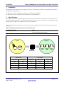
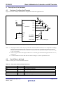
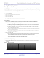
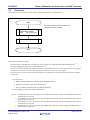
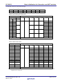
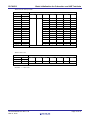
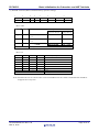
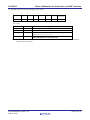
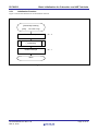
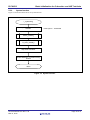
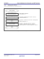
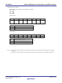
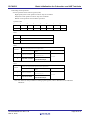
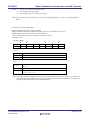
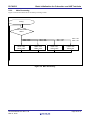
APPLICATION NOTE
RL78/G13
Basic Initialisation for Cubesuite+ and IAR Toolchain
R01AN1083EG0100
Rev.1.00
Mar 13, 2012
Introduction
This application note describes the basic setting items that are necessary for initializing the RL78/G13.
The sample program discussed in this application note initializes the RL78/G13 and provides on/off control of three
LEDs according to the combination of two switch input states.
Target Device
RL78/G13
When applying the sample program covered in this application note to another microcomputer, modify the program
according to the specifications for the target microcomputer and conduct an extensive evaluation of the modified
program.
This application note has been updated for the RSKRL78/G13 hardware platform.
R01AN1083EG0100 Rev.1.00
Mar 13, 2012
Page 1 of 31
RL78/G13
Basic Initialisation for Cubesuite+ and IAR Toolchain
Contents
1.
Installation ......................................................................................................................................... 3
2.
Specifications .................................................................................................................................... 3
3.
Operation Check Conditions ............................................................................................................. 4
4. Description of the Hardware.............................................................................................................. 5
4.1 Hardware Configuration Example ..................................................................................................... 5
4.2 List of Pins to be Used ...................................................................................................................... 5
5. Description of the Software ............................................................................................................... 6
5.1 Operation Outline .............................................................................................................................. 6
5.2 List of Option Byte Settings............................................................................................................... 7
5.3 List of Functions ................................................................................................................................ 7
5.4 Function Specifications ..................................................................................................................... 8
5.5 Flowcharts ....................................................................................................................................... 10
5.5.1
Initialization Function.............................................................................................................. 17
5.5.2
System function...................................................................................................................... 18
5.5.3
Setting up the I/O Ports [TODO] ............................................................................................ 19
5.5.4
CPU Clock Setup ................................................................................................................... 23
5.5.5
Main Processing..................................................................................................................... 29
6.
Sample Code................................................................................................................................... 30
7.
Documents for Reference ............................................................................................................... 30
Website and Support ............................................................................................................................... 31
Revision Record ........................................................................................................................................ 1
General Precautions in the Handling of MPU/MCU Products ................................................................... 2
R01AN1083EG0100 Rev.1.00
Mar 13, 2012
Page 2 of 31
RL78/G13
1.
Basic Initialisation for Cubesuite+ and IAR Toolchain
Installation
This application note and associated code has been written to work with both Cubesuite+ and IAR IDEs and compilers.
Decompress (if zipped) the files.
For Cubesuite+: Open the .mtpj project in the \CS+ Code directory in Cubesuite+
For IAR: Open the .eww workspace in the \IAR directory in IAR Workbench.
2.
Specifications
The sample program described in this application note performs basic initialization steps such as the setup of the clock
frequency and input/output ports. After the initialization, the program controls, in its main processing routine, the on/off
of three LEDs according to the combination of two switch input states.
Table 2.1 lists the Peripheral Functions to be Used and their Uses and figure 2.1 shows the outline of the initialization
processing.
Table 2.1 Peripheral Functions to be Used and their Uses
Peripheral Function
Use
Port input/output
Switch input (SW1 and SW2)
LED on/off control (LED1 to LED3)
<Input>
<Output>
ON
SW1
LED1
SW2
LED2
LED3
RL78/G13
LED Output
Switch Input
SW1 (P50)
SW2 (P51)
LED1 (P53)
LED2 (P62)
LED3 (P63)
OFF
OFF
OFF
OFF
OFF
ON
OFF
ON
OFF
OFF
OFF
ON
OFF
ON
OFF
ON
ON
OFF
OFF
ON
Figure 2.1 Overview of LVD Operation (Reset Mode)
R01AN1083EG0100 Rev.1.00
Mar 13, 2012
Page 3 of 31
RL78/G13
3.
Basic Initialisation for Cubesuite+ and IAR Toolchain
Operation Check Conditions
The sample code contained in this application note has been checked under the conditions listed in the table below.
Table 3.1 Operation Check Conditions
Item
Microcontroller used
Operating frequency
Operating voltage
Integrated development environments
C compiler
R01AN1083EG0100 Rev.1.00
Mar 13, 2012
Description
RL78/G13 (R5F100LEA)
• High-speed on-chip oscillator (HOCO) clock: 32 MHz
• CPU/peripheral hardware clock: 32 MHz
5.0 V (can run on a voltage range of 2.9 V to 5.5 V.)
• LVD operation (VLVIH): Reset mode 2.81 V (2.76 V to 2.87 V)
CubeSuite+ V1.00.01 from Renesas Electronics Corp.
IAR Embedded Workbench for Renesas RL78 version 1.10.4
CA78K0R V1.20 from Renesas Electronics Corp.
ICCRL78 V1.10.4 C/C++ Compiler for Renesas RL78 From IAR
Page 4 of 31
RL78/G13
4.
4.1
Basic Initialisation for Cubesuite+ and IAR Toolchain
Description of the Hardware
Hardware Configuration Example
Figure 4.1 shows an example of the hardware configuration used for this application note.
VDD
VDD
RESET
VDD
LED0
VDD
P52
EVDD
LED1
VDD
P53
VDD
RL78/G13
LED2
VDD
P62
LED3
P63
VDD
REGC
SW2
EVSS
P51/INTP2
VSS
P50/INTP1
P40/TOOL0
SW1
For on-chip debugger
Figure 4.1 Hardware Configuration
Notes 1: The purpose of this circuit is only to provide the connection outline and the circuit is simplified accordingly.
When designing and implementing an actual circuit, provide proper pin treatment and make sure that the
hardware's electrical characteristics conditions are met (connect the input-dedicated ports separately to VDD
or VSS via a resistor).
2: Connect any pins whose name begins with EVSS to VSS and any pins whose name begins with EVDD to VDD,
respectively.
3: VDD must be held at not lower than the reset release voltage (VLVI) that is specified as LVD.
4.2
List of Pins to be Used
Table 4.1 lists the pins to be used and their functions.
Table 4.1 Pins to be Used and Their Functions
Pin Name
P52
P53
P62
P63
P50/INTP1
P51/INTP2
I/O
Output
Output
Output
Output
Input
Input
R01AN1083EG0100 Rev.1.00
Mar 13, 2012
Description
LED on (LED0) control port
LED on (LED1) control port
LED on (LED2) control port
LED on (LED3) control port
Switch input (SW1) port
Switch input (SW2) port
Page 5 of 31
RL78/G13
5.
Basic Initialisation for Cubesuite+ and IAR Toolchain
Description of the Software
5.1
Operation Outline
The sample program described in this application note initializes the CPU (e.g., selecting the CPU clock frequency) and
sets up its I/O ports.
After completing the hardware setup, the sample program controls the on/off of three LEDs (LED1 to LED3) according
to the combination of states of two switch inputs (SW1 and SW2).
(1)
CPU initialization*
z
Sets up the peripheral I/O redirection function.
z
Sets up the I/O ports.
z
Sets up the CPU clock.
Note: The option bytes are referenced before the CPU is initialized.
<Setup conditions>
z
Sets the reset value because the CPU does not use the peripheral I/O redirection function (PIOR register).
z
Makes the following configurations for the I/O ports:
(1) Configures the ports that are configured for analog input after the release of the reset state for digital I/O
(ADPC register and port mode control register).
(2) Configures P50 and P51 which are to be used as switch inputs (SW1 and SW2) for input and the other
ports for output (port mode register).
(3) Connects on-chip pull-up resistors to P50 and P51 which are to be used as switch inputs (SW1 and SW2)
(pull-up resistor option register).
(4) Sets P53, P62, P63 which are to be used for on/off control of LEDs (LED1 to LED3) to 1 and the other
unused pins to 0 (port register).
z
Sets up the CPU clock.
(1) Sets the reset value because the high-speed system clock and subsystem clock are not to be in use (clock
operation mode control (CMC) register and clock operation status control (CSC) register).
(2) Selects the main system clock (fMAIN) as the CPU/peripheral hardware clock (fCLK) and HOCO (fIH) as the
main system clock (fMAIN) (system clock control (CKC) register).
(2) Executes the main processing.
z
Performs the LED output control as summarized in Table 4.1 according to the state of the switch inputs (SW1
and SW2).
Table 4.1 Main Processing
Switch Input
LED Output
SW1 (P50)
SW2 (P51)
LED1 (P53)
LED2 (P62)
OFF
OFF
OFF
OFF
ON
OFF
ON
OFF
OFF
ON
OFF
ON
ON
ON
OFF
OFF
Note: Refer to RL78/G13 User's Manual for notes on device use.
R01AN1083EG0100 Rev.1.00
Mar 13, 2012
LED3 (P63)
OFF
OFF
OFF
ON
Page 6 of 31
RL78/G13
5.2
Basic Initialisation for Cubesuite+ and IAR Toolchain
List of Option Byte Settings
Table 4.2 summarizes the settings of the option bytes.
Table 4.2 Option Byte Settings
Address
000C0H/010C0H
Value
01101110B
000C1H/010C1H
000C2H/010C2H
000C3H/010C3H
01111111B
11101000B
10000100B
5.3
Description
Stops the watchdog timer operation.
(Stops counting after the release of the reset state.)
LVD reset mode 2.81 V (2.76 V to 2.87 V)
HS mode HOCO: 32 MHz
Enables the on-chip debugging function.
List of Functions
Table 4.3 lists the functions that are used by this sample program.
Table 4.3 Functions
Function Name
[Cubesuite]: hdwinit
[IAR]: __low_level_init
R_Systeminit
R_PORT_Create
R_CGC_Create
main
R01AN1083EG0100 Rev.1.00
Mar 13, 2012
Outline
Initializes the hardware settings.
Calls the hardware initialization functions.
Initializes the I/O ports.
Initializes the clock generator.
Main function
Page 7 of 31
RL78/G13
5.4
Basic Initialisation for Cubesuite+ and IAR Toolchain
Function Specifications
This section describes the specifications for the functions that are used in the sample code.
[Function Name] hdwinit
Synopsis
Header
Declaration
Explanation
Arguments
Return value
Remarks
Initialize hardware settings.
r_cg_macrodriver.h
r_cg_cgc.h
r_cg_port.h
r_cg_userdefine.h
void hdwinit(void)
Performs the following operations:
(1) Executes the DI instruction.
(2) Executes the function R_Systeminit().
(3) Executes the EI instruction.
None
None
This function is called by the startup routine.
[Function Name] R_Systeminit
Synopsis
Header
Declaration
Explanation
Arguments
Return value
Remarks
Call hardware initialization functions.
r_cg_macrodriver.h
r_cg_cgc.h
r_cg_port.h
r_cg_userdefine.h
void R_Systeminit(void)
Performs the following operations:
(1) Sets the initial value of the peripheral I/O redirection register (PIOR).
(2) Executes the function R_PORT_Create().
(3) Executes the function R_CGC_Create().
(4) Sets the initial value of the flash memory CRC control register (CRC0CTL).
(5) Sets the initial value of the invalid memory access detection control register (IAWCTL).
None
None
[Function Name] R_PORT_Create
Synopsis
Header
Declaration
Explanation
Arguments
Return value
Remarks
Initialize I/O ports.
r_cg_macrodriver.h
r_cg_port.h
r_cg_userdefine.h
void R_PORT_Create(void)
Configures P50 and P51 for input (enabling the on-chip pull-up resistor) and P53, P62, and
P63 for output (high-level output). Configures the other ports except pin P40 for output (lowlevel output).
None
None
R01AN1083EG0100 Rev.1.00
Mar 13, 2012
Page 8 of 31
RL78/G13
Basic Initialisation for Cubesuite+ and IAR Toolchain
[Function Name] R_CGC_Create
Synopsis
Header
Declaration
Explanation
Arguments
Return value
Remarks
Initialize the clock generator.
r_cg_macrodriver.h
r_cg_cgc.h
r_cg_userdefine.h
void R_CGC_Create(void)
Initializes the registers related to the clock generator.
• None
• None
[Function Name] main
Synopsis
Header
Declaration
Explanation
Main function
r_cg_macrodriver.h
r_cg_cgc.h
r_cg_port.h
r_cg_userdefine.h
void main(void)
main function of the C language
Places the following outputs on the LEDs according to the values of SW1 (P50) and SW2
(P51):
SW2:SW1
0:0
0:1
1:0
1:1
Arguments
Return value
Remarks
: LED Binary Value
: 0b00000011
: 0b00000101
: 0b00000110
: 0b00000111
None
None
R01AN1083EG0100 Rev.1.00
Mar 13, 2012
Page 9 of 31
RL78/G13
5.5
Basic Initialisation for Cubesuite+ and IAR Toolchain
Flowcharts
Shown below is the overall flow of the sample program described in this application note.
Start
The option bytes are referenced before the
initialization function is called.
Initialisation function
[Cubesuite]: hdwinit()
[IAR]: __low_level_init()
main()
End
Figure 4.1 Overall Flow
Option byte configuration outline
The option bytes of the RL78/G13 are made up of user option bytes (000C0H-000C2H/010C0H-010C2H* 1 * 2 *3)
and on-chip debugging option bytes (000C3H/010C3H * 4).
The option bytes are automatically referenced and the prespecified functions are set up when power is first supplied
or after the release of the reset state. The option bytes cannot be set up by any user program.
The option bytes can exercise the controls listed below. They must be set up without fail before the microcomputer
is to be used.
User option bytes
• Makes settings related to the watchdog timer (000C0H/010C0H*1).
• Makes LVD-related settings (000C1H/010C1H*2).
• Sets up the HOCO and flash memory (000C2H/010C2H*3).
On-chip debugging option bytes (000C3H/010C3H*4)
Notes: 1. 010C0H must also set to be the same value as 000C0H because the contents of 000C0H and 010C0H are
swapped at boot swap time.
2. 010C1H must also set to be the same value as 000C1H because the contents of 000C1H and 010C1H are
swapped at boot swap time.
3. 010C2H must also set to be the same value as 000C2H because the contents of 000C2H and 010C2H are
swapped at boot swap time.
4. 010C3H must also set to be the same value as000C3H because the contents of 000C3H and 010C3H are
swapped at boot swap time.
R01AN1083EG0100 Rev.1.00
Mar 13, 2012
Page 10 of 31
RL78/G13
Basic Initialisation for Cubesuite+ and IAR Toolchain
The option bytes can be specified through "User Option Byte Values" on the "Device" panel on the CubeSuite+
"Link Option" tag.
Note: For details on the procedure for setting up the CubeSuite+ link options, refer to the CubeSuite+ tutorial.
R01AN1083EG0100 Rev.1.00
Mar 13, 2012
Page 11 of 31
RL78/G13
Basic Initialisation for Cubesuite+ and IAR Toolchain
(1) 000C0H / 010C0H* (watchdog timer related settings)
7
6
WDTINT
5
4
3
WINDOW1 WINDOW0 WDTON
0
1
1
2
1
0
WDCS2
WDCS1
WDCS0
WDSTBON
1
1
1
0
0
Bit 0
WDSTBYON
Control of watchdog timer counter
0
Disables counter operation in HALT/STOP
mode.
1
Enables counter operation in HALT/STOP mode.
Bits 3 to 1
WDCS2-0
Watchdog timer overflow time
6
000
2 /fIL
001
2 /fIL
010
2 /fIL
011
2 /fIL
100
2 /fIL
101
2 fIL
110
2 /fIL
111
2 /fIL
7
8
9
11
13
14
16
Bit 4
WDTON
Control of watchdog timer counter
Disables counter operation.
0
(Stops counter after the release of reset
sequence.)
Enables counter operation.
1
(Starts counter after the release of reset
sequence.)
Bits 6 to 5
WINDOW1
WINDOW0
Watchdog timer window open period
00
Setting prohibited
01
50%
10
75%
11
100%
Bit 7
WDTINT
0
1
Use of interval interrupts
Interval interrupt is not used.
An interval interrupt is generated when 75% is
reached.
Note: 010C0H must also set to be the same value as 000C0H because the contents of 000C0H and 010C0H are
swapped at boot swap time.
R01AN1083EG0100 Rev.1.00
Mar 13, 2012
Page 12 of 31
RL78/G13
Basic Initialisation for Cubesuite+ and IAR Toolchain
(2) 000C1H / 010C1H* (LVD-related settings)
7
6
5
4
3
2
1
0
VPOC2
VPOC1
VPOC0
1
LVIS1
LVIS0
LVIMDS1
LVIMDS0
0
1
1
1
1
1
1
1
When use as interrupt & reset mode
Detection Voltage
VLVIH
Option Byte Setting Value
VLVIL
Rising
edge
LVIMDS1
LVIMDS0
VPOC2
VPOC1
VPOC0
LVIS1
LVIS0
1
0
Falling
edge
Falling
edge
1.77 V
1.73 V
1.63 V
1.88 V
1.84 V
0
1
2.92 V
2.86 V
0
0
1.98 V
1.94 V
2.09 V
2.04 V
1
0
0
0
1.84 V
0
0
0
1
1
0
0
1
0
0
1
0
3.13 V
3.06 V
2.61 V
2.55 V
2.71 V
2.65 V
0
1
3.75 V
3.67 V
0
0
2.92 V
2.86 V
1
0
3.02 V
2.96 V
0
1
4.06 V
3.98 V
0
0
LVIS1
LVIS0
0
2.45 V
0
2.75 V
Other than above
1
0
1
1
Setting prohibited
When used as reset mode
Detection Voltage
Option Byte Setting Value
VLVIH
LVIMDS1
VLVIL
LVIMDS0
VPOC2
VPOC1
VPOC0
Rising edge Falling edge
1.67 V
1.63 V
0
0
0
1
1
1.77 V
1.73 V
0
0
0
1
0
1.88 V
1.84 V
0
0
1
1
1
1.98 V
1.94 V
0
0
1
1
0
2.09 V
2.04 V
0
0
1
0
1
2.50 V
2.45 V
0
1
0
1
1
2.61 V
2.55 V
0
1
0
1
0
2.71 V
2.65 V
0
1
0
0
1
2.81 V
2.75 V
0
1
1
1
1
1
1
2.92 V
2.86 V
0
1
1
1
0
3.02 V
2.96 V
0
1
1
0
1
3.13 V
3.06 V
0
0
1
0
0
3.75 V
3.67 V
0
1
0
0
0
4.06 V
3.98 V
0
1
1
0
0
Other than above
Setting prohibited
Note: 010C1H must also set to be the same value as 000C1H because the contents of 000C1H and 010C1H are
swapped at boot swap time.
R01AN1083EG0100 Rev.1.00
Mar 13, 2012
Page 13 of 31
RL78/G13
Basic Initialisation for Cubesuite+ and IAR Toolchain
When used as interrupt mode
Detection Voltage
VLVIH
VLVIL
Rising edge
Falling edge
1.67 V
1.77 V
1.63 V
1.73 V
1.88 V
Option Byte Setting Value
LVIMDS1 LVIMDS0
VPOC2
VPOC1
VPOC0
LVIS1
LVIS0
0
0
0
0
0
0
1
1
1
0
1.84 V
0
0
1
1
1
1.98 V
1.94 V
0
0
1
1
0
2.09 V
2.04 V
0
0
1
0
1
2.50 V
2.45 V
0
1
0
1
1
2.61 V
2.55 V
0
1
0
1
0
2.71 V
2.65 V
0
1
0
0
1
2.81 V
2.75 V
0
1
1
1
1
2.92 V
2.86 V
0
1
1
1
0
3.02 V
2.96 V
3.13 V
3.06 V
0
0
1
0
1
1
0
0
1
0
3.75 V
3.67 V
0
1
0
0
0
4.06 V
3.98 V
0
1
1
0
0
LVIS1
LVIS0
×
×
1
1
Other than above
Setting prohibited
When LVD is off
Detection Voltage
Option Byte Setting Value
VLVIH
LVIMDS1 LVIMDS0 VPOC2
VLVIL
VPOC1
VPOC0
Rising edge Falling edge
⎯
⎯
Other than above
0/1
1
1
×
×
Setting prohibited
Remarks: × = don’t care
R01AN1083EG0100 Rev.1.00
Mar 13, 2012
Page 14 of 31
RL78/G13
Basic Initialisation for Cubesuite+ and IAR Toolchain
(3) 000C2H / 010C2H* (HOCO and flash memory operation settings)
7
6
5
CMODE1 CMODE0
1
1
4
3
1
0
1
0
2
1
0
FRQSEL3 FRQSEL2 FRQSEL1 FRQSEL0
1
0
0
0
Bits 7 and 6
CMODE1 CMODE0 Setting of Flash Memory Operating Mode
0
1
1
Operating
Frequency Range
Operating
Voltage Range
0
LV (low voltage main)
mode
1 MHz to 4 MHz
1.6 V to 5.5 V
0
LS (low speed main)
mode
1 MHz to 8 MHz
1.8 V to 5.5 V
1
Other than above
HS (high speed main) 1 MHz to 16 MHz
mode
1 MHz to 32 MHz
2.4 V to 5.5 V
2.7 V to 5.5 V
Setting prohibited
Bits 3 to 0
FRQSEL3 FRQSEL2 FRQSEL1 FRQSEL0 HOCO Frequency
1
0
0
0
32 MHz
0
0
0
0
24 MHz
1
0
0
1
16 MHz
0
0
0
1
12 MHz
1
0
1
0
8 MHz
1
0
1
1
4 MHz
1
1
0
1
1 MHz
Other than above
Setting prohibited
Note: 010C2H must also set to be the same value as 000C2H because the contents of 000C2H and 010C2H are
swapped at boot swap time.
R01AN1083EG0100 Rev.1.00
Mar 13, 2012
Page 15 of 31
RL78/G13
Basic Initialisation for Cubesuite+ and IAR Toolchain
(4) 000C3H / 010C3H* (On-chip debugging option bytes)
7
6
5
4
3
2
1
0
OCDENSE
T
0
0
0
0
1
0
OCDERSD
1
0
0
0
0
1
0
1
Bits 7 and 0
OCDENSET
OCDERSD
Control of On-chip Debugging Operation
0
0
Disables on-chip debugging.
0
1
Setting prohibited
1
0
Enables operation and erases flash memory data when
authentication of security ID fails.
1
1
Enables operation but does not erase flash memory data
when authentication of security ID fails.
Note: 010C3H must also set to be the same value as 000C3H because the contents of 000C3H and 010C3H are
swapped at boot swap time.
R01AN1083EG0100 Rev.1.00
Mar 13, 2012
Page 16 of 31
RL78/G13
5.5.1
Basic Initialisation for Cubesuite+ and IAR Toolchain
Initialization Function
Figure 4.2 shows the flowchart for the initialization function.
[Cubesuite]: hdwinit()
[IAR]:
low level init()
Disable interrupts
IE ← 0
System function
r_systeminit()
Enable interrupts
IE ← 1
return
Figure 4.2 Initialization Function
R01AN1083EG0100 Rev.1.00
Mar 13, 2012
Page 17 of 31
RL78/G13
5.5.2
Basic Initialisation for Cubesuite+ and IAR Toolchain
System function
Figure 4.3 shows the flowchart for the system function.
r_systeminit()
Disuse peripheral I/O redirection
function
PIOR register ← 00000000B
Set up I/O ports
PORT_Create()
Set up CPU clock
R_CGC_Create()
Stop CRC calculator
Disable detection of invalid memory
access
return
Figure 4.3 System Function
R01AN1083EG0100 Rev.1.00
Mar 13, 2012
Page 18 of 31
RL78/G13
5.5.3
Basic Initialisation for Cubesuite+ and IAR Toolchain
Setting up the I/O Ports
Figure 4.4 shows the flowchart for setting up the I/O ports.
PORT_Create()
Configure analog input alternatefunction pins for digital I/O
Set up port mode register
Set up pull-up resistor option
register
Set up port register
ADPC register ← 00000001B
PMC register bits ← 0
PM5 register ← 00000011B : P51 and P50 → Input port
Other PMx register bits ← 0
PU5 register ← 00000011B : P51 and P50 → Internally pulled
up
Other PUx register bits ← 0
P5 register ← 00001100B : P52 to P53 → Output "H"
P6 register ← 00001100B : P62 to P63 → Output "H"
Other Px register bits ← 0: Other Px register bits → Output "L"
return
Figure 4.4 I/O Port Setup
R01AN1083EG0100 Rev.1.00
Mar 13, 2012
Page 19 of 31
RL78/G13
Basic Initialisation for Cubesuite+ and IAR Toolchain
Outline of I/O port setup
The RL78/G13 is equipped with digital I/O ports so that it can provide a variety of controls.
The I/O ports serve multiple pin functions in addition to serving as digital I/O ports.
The I/O ports are controlled by the registers listed below. They must be set up during the system initialization
routine that is executed when power is first supplied or after the release of the reset state.
Registers that are used to manipulate ports:
•
•
•
•
•
•
•
•
•
Port mode register (PMxx)
Port register (Pxx)
Pull-up resistor option register (PUxx)
Port input mode register (PIMx)
Port output mode register (POMx)
Port mode control register (PMCxx)*
A/D port configuration register (ADPC)*
Peripheral I/O redirection register (PIOR)
Global digital input disable register (GDIDIS)
Note:
A register used to place port pins in digital I/O or analog input mode. Since the port pins are configured for
analog input when a reset signal occurs, the pins that are to be used for digital I/O must always be set up
with this register after the release of the reset state. For the sample program described in this application
note, all port pins are configured for digital I/O.
Notes 1. Refer to RL78/G13 User's Manual: Hardware for the procedure to set up registers to configure ports as
alternate-function pins for peripheral functions.
2. Provide proper treatment for unused pins so that their electrical specifications are observed. Connect each
of any unused input-only ports to VDD or VSS via a resistor.
3. Connect any pins whose name begins with EVSS to VSS and any pins whose name begins with EVDD to
VDD, respectively.
Given below is an example of manipulating ports that are used in this sample code.
R01AN1083EG0100 Rev.1.00
Mar 13, 2012
Page 20 of 31
RL78/G13
Basic Initialisation for Cubesuite+ and IAR Toolchain
Setting up ports for LEDs
• Port mode register 5 (PM5), Port mode register 6 (PM6)
P52: LED0
P53: LED1
P62: LED2
P63: LED3
Symbol: PM5
7
6
5
4
3
2
1
PM57
PM56
PM55
PM54
PM53
PM52
0
0
0
0
0
0
0
PM51
PM50
1
1
(See SW2) (See SW1)
PM5n
PM5n pin I/O mode selection.
0
Output mode (output buffer on)
1
Input mode (output buffer off)
Symbol: PM6
7
6
5
4
3
2
1
0
PM67
PM66
PM65
PM64
PM63
PM62
PM61
PM60
0
0
0
0
0
0
0
0
PM6n
PM6n pin I/O mode selection.
0
Output mode (output buffer on)
1
Input mode (output buffer off)
Notes 1. This sample code configures any unused ports for output to minimize the adverse influence of through
current.
2. For details on the procedure for setting up the registers, refer to RL78/G13 User's Manual: Hardware.
R01AN1083EG0100 Rev.1.00
Mar 13, 2012
Page 21 of 31
RL78/G13
Basic Initialisation for Cubesuite+ and IAR Toolchain
Setting up ports for switches
• Port mode register 5 (PM5)
• Pull-up resistor option register 0 (PU0)
P50: SW1 P51: SW2
• Port mode control register 0 (PMC0)
Digital input
Symbol: PM5
7
6
5
4
3
PM57
PM56
PM55
PM54
0
0
0
0
2
1
0
PM53
PM52
PM51
PM50
0
0
1
1
(See LED1) (See LED0)
PM5n
PM5n pin I/O mode selection.
0
Output mode (output buffer on)
1
Input mode (output buffer off)
Symbol: PU5
7
6
5
4
3
2
1
0
0
PU56
PU55
PU54
PU53
PU52
PU51
PU50
0
0
0
0
0
0
1
1
PU0n
Selection of on-chip pull-up resistor for P0n pin.
0
On-chip pull-up resistor not connected.
1
On-chip pull-up resistor connected.
Notes 1. This sample code configures any unused ports for output to minimize the adverse influence of through
current.
2. For details on the procedure for setting up the registers, refer to RL78/G13 User's Manual: Hardware.
R01AN1083EG0100 Rev.1.00
Mar 13, 2012
Page 22 of 31
RL78/G13
5.5.4
Basic Initialisation for Cubesuite+ and IAR Toolchain
CPU Clock Setup
Figure 4.5 shows the flowchart for setting up the CPU clock.
R_CGC_Create()
CMC register ← 00000000B
MSTOP bit ← 1: Does not use high-speed system clock.
XTSTOP bit ← 1: Does not use subsystem clock.
Set up high-speed system
clock/subsystem clock
MCM0 bit ← 1: Selects high-speed OCO clock (fIH) as system clock
(fMAIN).
CSS bit ← 1: Selects main system clock (fMAIN) as CPU/peripheral
hardware clock (fCLK).
Select CPU/peripheral hardware
clock (fCLK)
return
Figure 4.5 CPU Clock Setup
Outline of CPU clock setup
The RL78/G13 allows the user to select the system clock source from the high-speed on-chip oscillator (HOCO),
main system clock oscillator/external clock input, and subsystem clock oscillator/external clock input*1.
The system clock is controlled by the registers listed below.
The CPU clock must be initialized during the system initialization routine that is executed when power is first
supplied or after the release of the reset state.
Registers that are used to initialize the CPU clock:
• Clock operation mode control register (CMC)
• Clock operation status control register (CSC)
• System clock control register (CKC)
• Peripheral enable register 0 (PER0)
• Operation speed mode control register (OSMC)
Note: Selectable only for 40-, 44-, 48-, 52-, 64-, 80-, 100-, and 128-pin products.
Given below is an example of setting up the CPU clock for this sample code.
R01AN1083EG0100 Rev.1.00
Mar 13, 2012
Page 23 of 31
RL78/G13
Basic Initialisation for Cubesuite+ and IAR Toolchain
Setting up the clock operating mode
• Clock operation mode control register (CMC)
High-speed system clock pin's operating mode: Input port mode
Subsystem clock pin's operating mode: Input port mode
XT1 oscillator oscillation mode: Low power consumption oscillation
X1 clock oscillation frequency control: 1 MHz ≤ fMX ≤ 10 MHz
Symbol: CMC
7
6
5
4
3
2
1
0
EXCLK
OSCSEL
EXCLKS
OSCSELS
0
AMPHS1
AMPHS0
AMPH
0
0
0
0
0
0
0
0
Bit 0
AMPH
Control of X1 clock oscillation frequency
0
1 MHz ≤ fMX ≤ 10 MHz
1
10 MHz < fMX ≤ 20 MHz
Bits 2 and 1
AMPHS1 AMPHS0
Selection of oscillation mode for XT1
oscillator
0
0
Low power consumption oscillation
(default)
0
1
Normal oscillation
1
×
Ultra-low power consumption oscillation
Bits 5 and 4
EXCLKS
OSCSELS
0
0
Subsystem Clock Pin
Operating Mode
XT1/P123 Pin
Input port mode
Input port
XT2/EXCLKS/P124 Pin
0
1
XT1 oscillation mode
Connected to crystal oscillator
1
0
Input port mode
Input port
1
1
External clock input mode
Input port
External clock input
High-speed System Clock
Pin Operating Mode
X1/P121 Pin
X2/EXCLK/P122 Pin
Input port mode
Input port
Bits 7 and 6
EXCLK
OSCSEL
0
0
0
1
X1 oscillation mode
Connected to crystal/ceramic oscillator
1
0
Input port mode
Input port
1
1
External clock input mode
Input port
External clock input
Note: For details on the procedure for setting up the registers, refer to RL78/G13 User's Manual:
Hardware.
R01AN1083EG0100 Rev.1.00
Mar 13, 2012
Page 24 of 31
RL78/G13
Basic Initialisation for Cubesuite+ and IAR Toolchain
Controlling clock operations
• Clock operation status control register (CSC)
High-speed system clock operation control: Stop X1 oscillator.
Subsystem clock operation control: Stop XT1 oscillator.
HOCO clock operation control: HOCO operation
Symbol: CSC
7
6
5
4
3
2
1
0
MSTOP
XTSTOP
0
0
0
0
0
HIOSTOP
1
1
0
0
0
0
0
0
Bit 0
HIOSTOP
Control of HOCO clock operation
0
Runs HOCO.
1
Stops HOCO.
Bit 6
Control of Subsystem Clock Operation
XTSTOP
XT1 Oscillation Mode
External Clock Input
Mode
0
Runs XT1 oscillator.
Enables external clock from
the EXCLKS pin.
1
Stops XT1 oscillator.
Disables external clock
from the EXCLK pin.
Input Port Mode
Input port
Bit 7
Control of High-speed System Clock Operation
MSTOP
X1 Oscillation Mode
External Clock Input
Mode
0
Runs X1 oscillator.
Enables external clock from
the EXCLKS pin.
1
Stops X1 oscillator.
Disables external clock
from the EXCLK pin.
Input Port Mode
Input port
Note: For details on the procedure for setting up the registers, refer to RL78/G13 User's Manual:
Hardware.
R01AN1083EG0100 Rev.1.00
Mar 13, 2012
Page 25 of 31
RL78/G13
Basic Initialisation for Cubesuite+ and IAR Toolchain
Setting up the CPU/peripheral hardware clock (fCLK)
• System clock control register (CKC)
fCLK status: Main system clock
fCLK selection: HOCO clock (fIH)
Symbol: CKC
7
6
5
4
3
2
1
0
CLS
CSS
MCS
MCM0
0
0
0
0
0
0
0
0
0
0
0
0
Bit 4
MCM0
Control of main system clock (fMAIN) operation
0
Selects HOCO clock (fIH) as the main system cock (fMAIN).
1
Selects high-speed system clock (fMX) as the main system clock (fMAIN).
Bit 5
MCS
Main system clock (fMAIN) state
0
HOCO clock (fIH)
1
High-speed system clock (fMX)
Bit 6
CSS
Selection of CPU/peripheral hardware clock( fCLK)
0
Main system clock (fMAIN)
1
Subsystem clock (fSUB)
Bit 7
CLS
CPU/peripheral hardware clock (fCLK) state
0
Main system clock (fMAIN)
1
Subsystem clock (fSUB)
Note: For details on the procedure for setting up the registers, refer to RL78/G13 User's Manual:
Hardware.
R01AN1083EG0100 Rev.1.00
Mar 13, 2012
Page 26 of 31
RL78/G13
Basic Initialisation for Cubesuite+ and IAR Toolchain
Setting use/disuse of peripheral hardware macros
• Peripheral enable register 0 (PER0)
Hardware input clock control: Stop input clocks.
Symbol: PER0
7
6
RTCEN
5
IICA1EN
0
*1
4
ADCEN
0
3
IICA0EN
0
*2
2
SAU1EN
0
0
*3
1
SAU0EN
0
0
TAU1EN
0
*1
TAU0EN
0
Bits 1 and 0
TAUmEN
Control of timer array unit m input clock
Stops supply of input clock.
0
• SFR for timer array unit m cannot be written.
• Timer array unit m is in the reset state.
1
Supplies input clock.
SFR for timer array unit m can be read and written.
Bits 3 and 2
SAUmEN
Control of serial array unit m input clock
Stops supply of input clock.
0
• SFR for serial array unit m cannot be written.
• Serial array unit m is in the reset state.
1
Supplies input clock.
SFR for serial array unit m can be read and written.
Bits 6 and 4
IICAmEN
Control of serial interface IICAm input clock
Stops supply of input clock.
0
• SFR for IICAm cannot be written.
• IICAm is in the reset state.
1
Supplies input clock.
SFR for IICAm can be read and written.
Bit 5
ADCEN
Control of A/D converter input clock
Stops supply of input clock.
0
• SFR for A/D converter cannot be written.
• A/D converter is in the reset state.
1
Supplies input clock.
SFR for A/D converter can be read and written.
Bit 7
RTCEN
Control of realtime clock (RTC) input clock
Stops supply of input clock.
0
• SFR for RT cannot be written.
• RTC is in the reset state.
1
Supplies input clock.
SFR for RTC can be read and written.
R01AN1083EG0100 Rev.1.00
Mar 13, 2012
Page 27 of 31
RL78/G13
Basic Initialisation for Cubesuite+ and IAR Toolchain
Notes: 1. For 80-, 100-, and 128-pin products only.
2. Not installed in 20-pin products.
3. Not installed in 20-, 24-, and 25-pin products.
Note: Power saving and noise reduction are achieved by stopping the supply of clocks to any unused hardware
macros.
Controlling the operation speed mode
• Operation speed mode control register (OSMC)
Setting in STOP mode or HALT mode while subsystem clock is selected as CPU clock
: Enables supply of subsystem clock to peripheral functions.
Selection of operation clock for realtime clock and interval timer
: Subsystem clock
Symbol: OSMC
7
6
5
4
3
2
1
0
RTCLPC
0
0
WUTMMCK0
0
0
0
0
0
0
0
0
0
0
0
0
Bit 4
WUTMMCK0
Selection of operation clock for realtime clock and interval timer
0
Subsystem clock (fSUB)
1
Internal low-speed oscillator (LOCO) clock
Bit 7
RTCLPC
Setting in STOP Mode or HALT Mode while subsystem clock is selected as
CPU clock
0
Enables supply of subsystem clock to peripheral functions
1
Stops supply of subsystem clock to peripheral functions except the realtime
clock and interval timer.
Note: The OSMC register is designed to reduce the operating current, for low power operation, in STOP mode
and in HALT mode in which the CPU is running on the subsystem clock. For details on its configuration
procedure, refer to RL78/G13 User's Manual: Hardware.
R01AN1083EG0100 Rev.1.00
Mar 13, 2012
Page 28 of 31
RL78/G13
5.5.5
Basic Initialisation for Cubesuite+ and IAR Toolchain
Main Processing
Figure 4.6 shows the flowchart for the main processing routine.
main()
SW1 and SW2
state?
SW1 = OFF
SW2 = OFF
LED1: OFF
LED2: OFF
LED3: OFF
SW1 = ON
SW2 = OFF
LED1: ON
LED2: OFF
LED3: OFF
SW1 = OFF
SW2 = ON
LED1: OFF
LED2: ON
LED3: OFF
SW1 = ON
SW2 = ON
LED1: OFF
LED2: OFF
LED3: ON
Figure 4.6 Main Processing
R01AN1083EG0100 Rev.1.00
Mar 13, 2012
Page 29 of 31
RL78/G13
6.
Basic Initialisation for Cubesuite+ and IAR Toolchain
Sample Code
The sample code is available on the Renesas Electronics Website.
7.
Documents for Reference
RL78/G13 User's Manual: Hardware Rev.1.00 (R01UH0146EJ0100)
RL78 Family User's Manual: Software Rev.1.00 (R01US0015EJ0100)
RL78/G13 Renesas Starter Kit Users’s Manual Rev.1.00 (R20UT0459EG0100)
(The latest versions of the documents are available on the Renesas Electronics Website.)
Technical Updates/Technical Brochures
(The latest versions of the documents are available on the Renesas Electronics Website.)
R01AN1083EG0100 Rev.1.00
Mar 13, 2012
Page 30 of 31
RL78/G13
Basic Initialisation for Cubesuite+ and IAR Toolchain
Website and Support
Renesas Electronics Website
http://www.renesas.com/
Inquiries
http://www.renesas.com/inquiry
All trademarks and registered trademarks are the property of their respective owners.
R01AN1083EG0100 Rev.1.00
Mar 13, 2012
Page 31 of 31
Revision Record
Rev.
1.00
Date
Mar.13.2012
Description
Page
Summary
Ported from r01an0451ej0100
Ported to RSKRL78/G13 hardware
Added support for IAR
Updated Document template
First edition issued
A-1
General Precautions in the Handling of MPU/MCU Products
The following usage notes are applicable to all MPU/MCU products from Renesas. For detailed usage notes on the
products covered by this manual, refer to the relevant sections of the manual. If the descriptions under General
Precautions in the Handling of MPU/MCU Products and in the body of the manual differ from each other, the
description in the body of the manual takes precedence.
1. Handling of Unused Pins
Handle unused pins in accord with the directions given under Handling of Unused Pins in the manual.
⎯ The input pins of CMOS products are generally in the high-impedance state. In operation with an
unused pin in the open-circuit state, extra electromagnetic noise is induced in the vicinity of LSI, an
associated shoot-through current flows internally, and malfunctions occur due to the false
recognition of the pin state as an input signal become possible. Unused pins should be handled as
described under Handling of Unused Pins in the manual.
2. Processing at Power-on
The state of the product is undefined at the moment when power is supplied.
⎯ The states of internal circuits in the LSI are indeterminate and the states of register settings and
pins are undefined at the moment when power is supplied.
In a finished product where the reset signal is applied to the external reset pin, the states of pins
are not guaranteed from the moment when power is supplied until the reset process is completed.
In a similar way, the states of pins in a product that is reset by an on-chip power-on reset function
are not guaranteed from the moment when power is supplied until the power reaches the level at
which resetting has been specified.
3. Prohibition of Access to Reserved Addresses
Access to reserved addresses is prohibited.
⎯ The reserved addresses are provided for the possible future expansion of functions. Do not access
these addresses; the correct operation of LSI is not guaranteed if they are accessed.
4. Clock Signals
After applying a reset, only release the reset line after the operating clock signal has become stable.
When switching the clock signal during program execution, wait until the target clock signal has
stabilized.
⎯ When the clock signal is generated with an external resonator (or from an external oscillator)
during a reset, ensure that the reset line is only released after full stabilization of the clock signal.
Moreover, when switching to a clock signal produced with an external resonator (or by an external
oscillator) while program execution is in progress, wait until the target clock signal is stable.
5. Differences between Products
Before changing from one product to another, i.e. to one with a different type number, confirm that the
change will not lead to problems.
⎯ The characteristics of MPU/MCU in the same group but having different type numbers may differ
because of the differences in internal memory capacity and layout pattern. When changing to
products of different type numbers, implement a system-evaluation test for each of the products.
Notice
1.
All information included in this document is current as of the date this document is issued. Such information, however, is subject to change without any prior notice. Before purchasing or using any Renesas
Electronics products listed herein, please confirm the latest product information with a Renesas Electronics sales office. Also, please pay regular and careful attention to additional and different information to
be disclosed by Renesas Electronics such as that disclosed through our website.
2.
Renesas Electronics does not assume any liability for infringement of patents, copyrights, or other intellectual property rights of third parties by or arising from the use of Renesas Electronics products or
technical information described in this document. No license, express, implied or otherwise, is granted hereby under any patents, copyrights or other intellectual property rights of Renesas Electronics or
others.
3.
You should not alter, modify, copy, or otherwise misappropriate any Renesas Electronics product, whether in whole or in part.
4.
Descriptions of circuits, software and other related information in this document are provided only to illustrate the operation of semiconductor products and application examples. You are fully responsible for
the incorporation of these circuits, software, and information in the design of your equipment. Renesas Electronics assumes no responsibility for any losses incurred by you or third parties arising from the
use of these circuits, software, or information.
5.
When exporting the products or technology described in this document, you should comply with the applicable export control laws and regulations and follow the procedures required by such laws and
regulations. You should not use Renesas Electronics products or the technology described in this document for any purpose relating to military applications or use by the military, including but not limited to
the development of weapons of mass destruction. Renesas Electronics products and technology may not be used for or incorporated into any products or systems whose manufacture, use, or sale is
prohibited under any applicable domestic or foreign laws or regulations.
6.
Renesas Electronics has used reasonable care in preparing the information included in this document, but Renesas Electronics does not warrant that such information is error free. Renesas Electronics
7.
Renesas Electronics products are classified according to the following three quality grades: "Standard", "High Quality", and "Specific". The recommended applications for each Renesas Electronics product
assumes no liability whatsoever for any damages incurred by you resulting from errors in or omissions from the information included herein.
depends on the product's quality grade, as indicated below. You must check the quality grade of each Renesas Electronics product before using it in a particular application. You may not use any Renesas
Electronics product for any application categorized as "Specific" without the prior written consent of Renesas Electronics. Further, you may not use any Renesas Electronics product for any application for
which it is not intended without the prior written consent of Renesas Electronics. Renesas Electronics shall not be in any way liable for any damages or losses incurred by you or third parties arising from the
use of any Renesas Electronics product for an application categorized as "Specific" or for which the product is not intended where you have failed to obtain the prior written consent of Renesas Electronics.
The quality grade of each Renesas Electronics product is "Standard" unless otherwise expressly specified in a Renesas Electronics data sheets or data books, etc.
"Standard":
Computers; office equipment; communications equipment; test and measurement equipment; audio and visual equipment; home electronic appliances; machine tools;
personal electronic equipment; and industrial robots.
"High Quality": Transportation equipment (automobiles, trains, ships, etc.); traffic control systems; anti-disaster systems; anti-crime systems; safety equipment; and medical equipment not specifically
designed for life support.
"Specific":
Aircraft; aerospace equipment; submersible repeaters; nuclear reactor control systems; medical equipment or systems for life support (e.g. artificial life support devices or systems), surgical
implantations, or healthcare intervention (e.g. excision, etc.), and any other applications or purposes that pose a direct threat to human life.
8.
You should use the Renesas Electronics products described in this document within the range specified by Renesas Electronics, especially with respect to the maximum rating, operating supply voltage
range, movement power voltage range, heat radiation characteristics, installation and other product characteristics. Renesas Electronics shall have no liability for malfunctions or damages arising out of the
use of Renesas Electronics products beyond such specified ranges.
9.
Although Renesas Electronics endeavors to improve the quality and reliability of its products, semiconductor products have specific characteristics such as the occurrence of failure at a certain rate and
malfunctions under certain use conditions. Further, Renesas Electronics products are not subject to radiation resistance design. Please be sure to implement safety measures to guard them against the
possibility of physical injury, and injury or damage caused by fire in the event of the failure of a Renesas Electronics product, such as safety design for hardware and software including but not limited to
redundancy, fire control and malfunction prevention, appropriate treatment for aging degradation or any other appropriate measures. Because the evaluation of microcomputer software alone is very difficult,
please evaluate the safety of the final products or system manufactured by you.
10. Please contact a Renesas Electronics sales office for details as to environmental matters such as the environmental compatibility of each Renesas Electronics product. Please use Renesas Electronics
products in compliance with all applicable laws and regulations that regulate the inclusion or use of controlled substances, including without limitation, the EU RoHS Directive. Renesas Electronics assumes
no liability for damages or losses occurring as a result of your noncompliance with applicable laws and regulations.
11. This document may not be reproduced or duplicated, in any form, in whole or in part, without prior written consent of Renesas Electronics.
12. Please contact a Renesas Electronics sales office if you have any questions regarding the information contained in this document or Renesas Electronics products, or if you have any other inquiries.
(Note 1)
"Renesas Electronics" as used in this document means Renesas Electronics Corporation and also includes its majority-owned subsidiaries.
(Note 2)
"Renesas Electronics product(s)" means any product developed or manufactured by or for Renesas Electronics.
http://www.renesas.com
SALES OFFICES
Refer to "http://www.renesas.com/" for the latest and detailed information.
Renesas Electronics America Inc.
2880 Scott Boulevard Santa Clara, CA 95050-2554, U.S.A.
Tel: +1-408-588-6000, Fax: +1-408-588-6130
Renesas Electronics Canada Limited
1101 Nicholson Road, Newmarket, Ontario L3Y 9C3, Canada
Tel: +1-905-898-5441, Fax: +1-905-898-3220
Renesas Electronics Europe Limited
Dukes Meadow, Millboard Road, Bourne End, Buckinghamshire, SL8 5FH, U.K
Tel: +44-1628-585-100, Fax: +44-1628-585-900
Renesas Electronics Europe GmbH
Arcadiastrasse 10, 40472 Düsseldorf, Germany
Tel: +49-211-65030, Fax: +49-211-6503-1327
Renesas Electronics (China) Co., Ltd.
7th Floor, Quantum Plaza, No.27 ZhiChunLu Haidian District, Beijing 100083, P.R.China
Tel: +86-10-8235-1155, Fax: +86-10-8235-7679
Renesas Electronics (Shanghai) Co., Ltd.
Unit 204, 205, AZIA Center, No.1233 Lujiazui Ring Rd., Pudong District, Shanghai 200120, China
Tel: +86-21-5877-1818, Fax: +86-21-6887-7858 / -7898
Renesas Electronics Hong Kong Limited
Unit 1601-1613, 16/F., Tower 2, Grand Century Place, 193 Prince Edward Road West, Mongkok, Kowloon, Hong Kong
Tel: +852-2886-9318, Fax: +852 2886-9022/9044
Renesas Electronics Taiwan Co., Ltd.
13F, No. 363, Fu Shing North Road, Taipei, Taiwan
Tel: +886-2-8175-9600, Fax: +886 2-8175-9670
Renesas Electronics Singapore Pte. Ltd.
1 harbourFront Avenue, #06-10, keppel Bay Tower, Singapore 098632
Tel: +65-6213-0200, Fax: +65-6278-8001
Renesas Electronics Malaysia Sdn.Bhd.
Unit 906, Block B, Menara Amcorp, Amcorp Trade Centre, No. 18, Jln Persiaran Barat, 46050 Petaling Jaya, Selangor Darul Ehsan, Malaysia
Tel: +60-3-7955-9390, Fax: +60-3-7955-9510
Renesas Electronics Korea Co., Ltd.
11F., Samik Lavied' or Bldg., 720-2 Yeoksam-Dong, Kangnam-Ku, Seoul 135-080, Korea
Tel: +82-2-558-3737, Fax: +82-2-558-5141
© 2012 Renesas Electronics Corporation. All rights reserved.
Colophon 1.1