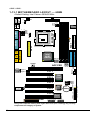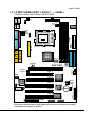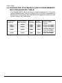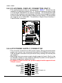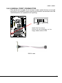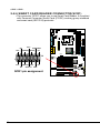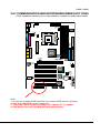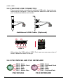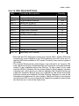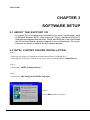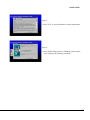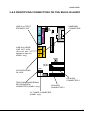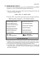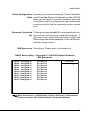
1
R
T h e
S o u l
O f
C o m p u t e r
T e c h n o l o g y
SL-65ME/65ME+ V1.1
USER MANUAL
USER NOTICE
T
Product Model
Manual Revision
Release Date
: SL-65ME/65ME+
: V1.1
: January 2001
his Users Guide & Technical Reference is for assisting system
manufacturers and end-users in setting up and installing the
motherboard.
Every effort has been made to ensure that the information in this
manual is accurate. Soltek Computer Inc. is not responsible for printing or clerical errors. Information in this document is subject to
change without notice and does not represent a commitment on the
part of Soltek Computer Inc.
No part of this manual may be reproduced, transmitted, translated
into any language in any form or by any means, electronic or
mechanical, including photocopying and recording, for any purpose
without the express written permission of Soltek Computer Inc.
Companies and products mentioned in this manual are for identification purpose only. Product names appearing in this manual may
or may not be registered trademarks or copyrights of their respective companies.
Soltek computer inc. Provides this manual “As is “ without warranty
of any kind, either express or implied, including but not limited to
the implied warranties or conditions of merchantability or fitness for
a particular purpose. In no event shall Soltek computer inc. Be liable for any loss or profits, loss of business, loss of use or data,
interruption of business, or for indirect, special, incidental, or consequential damages of any kind, even if Soltek computer inc. Has
been advised of the possibility of such damages arising from any
defect or error in this manual or product.
Copyright © 1996~2001 Soltek Computer Inc. All Rights Reserved.
• Intel, Celeron, Pentium II, Pentium III are trademarks of Intel Corporation.
• Intel 82815 Graphic Memory Controller Hub(GMCH), 82801 I/O Controller Hub(ICH) are trademarks of Intel Corporation.
• VIA Cyrix III is trademark of VIA Corporation.
• Norton AntiVirus, Norton Ghost are trademarks of Semantic Corporation.
SOLTEK AROUND THE WORLD
SOLTEK COMPUTER INC.
Address
Telephone
Fax
E-mail
Web site
: 7F, No. 306-3, Ta-Tung Rd, Sec.1, Hsi-Chin, TaipeiHsien, Taiwan, R.O.C.
: 886-2-2642-9060
: 886-2-2642-9065
: [email protected]
: http://www.soltek.com.tw
SOLTEK KOREA INC.
Address
Telephone
Fax
E-mail
: 1002, Chungjin Bldg. 53-5 Wonhyo-Ro, 3-Ka,
Yongsan-Ku Seoul 140-113, Korea
: 82-2-32717400
: 82-2-32717405
: [email protected]
SOUL TECHNOLOGY EUROPE B.V.
Address
Telephone
Fax
E-mail
Web site
: Sydneystraat 52-54 3047 BP Rotterdam, the Netherlands
: 31-10-2457492
: 31-10-2457493
: [email protected]
: http://www.soultech-europe.com
65ME / 65ME+
CONTENT
CHAPTER 1
INTRODUCTION ............................................................................ 7
1-1 ITEMLIST CHECKUP ............................................................................. 7
1-2 CPU ........................................................................................................ 7
1-3 CHIPSET ................................................................................................ 7
1-4 INTEGRATED SDRAM CONTROLLER ................................................. 7
1-5 BIOS ....................................................................................................... 8
1-6 MULTI-I/O FUNCTION ........................................................................... 8
1-7 POWER MANAGEMENT ....................................................................... 8
1-8 FULL FEATURED ACCELERATED GRAPHICS PORTS (AGP)
CONTROLLER ....................................................................................... 9
1-9 SOUND CONTROLLER ......................................................................... 9
1-10 FORM FACTOR ................................................................................... 9
1-11 EXTENSION SLOTS ............................................................................ 9
1-12 HARDWARE MONITORING ................................................................ 9
1-13.1 MOTHERBOARD LAYOUT --- 65ME .............................................. 10
1-13.2 MOTHERBOARD LAYOUT --- 65ME+ ............................................ 11
1-14 CHIPSET SYSTEM BLOCK DIAGRAM ............................................. 12
1-15 MOTHERBOARD SPECIFICATION TABLE OF 65ME & 65ME+ ...... 13
CHAPTER 2
HARDWARE SETUP ................................................................... 15
2-1 CPU INSTALLATION ............................................................................ 15
2-2 CPU FREQUENCY .............................................................................. 16
2-3 MEMORY INSTALLATION ................................................................... 17
2-4 SUPPORTED SYSTEM BUS AND SYSTEM MEMORY BUS FREQUENCIES
TABLE ................................................................................................... 18
2-5 ACCELERATED GRAPHICS PORT(AGP) PRO INSTALLATION ........ 19
2-6 HDD/FDD INSTALLATION ................................................................... 20
2-7 JUMPER DEFINITION ......................................................................... 21
2-7.1 ONBOARD FAN (CPUFAN1/AUXFA1/CHAFA1) .............................. 21
2-7.2 KEYBOARD POWER ON (JP1) ........................................................ 21
2-7.3 BUS CLOCK SELECT (JP5/JP6) ...................................................... 22
2-7.4 USB PORT SELECT(1) (JP2/JP8) .................................................... 22
2-7.5 USB PORT SELECT(2) JP9/JP10) ................................................... 22
2-7.6 USB WAKE UP FUNCTION (JP11) ................................................... 22
4
65ME / 65ME+
2-7.7 ONBOARD CREATIVE SOUND SELECT (JP21) ............................. 23
2-7.8 CLEAR CMOS DATA (JBAT1/JBAT2) ............................................... 23
2-7.9 BIOS BOOT BLOCK LOCK (JP16) ................................................... 23
2-7.10 WAKE ON LAN(WOL) FUNCTION (JWOL1) .................................. 24
2-7.11 CD-ROM AUDIO CONNECTOR (CD_IN1/CD_IN2) ........................ 24
2-7.12 TAD1/TV1 CONNECTOR ................................................................ 24
2-7.13 THERMAL SENSOR CONNECTOR (RT2) ..................................... 25
2-8 CONNECTORS .................................................................................... 26
2-8.1 J2J3 ................................................................................................... 26
2-8.2 CHASSIS PANEL CONNECTOR ...................................................... 29
2-8.3 FLAT-PANEL DISPLAY CONNECTOR (DVC1) ................................. 30
2-8.4 ATX POWER SUPPLY CONNECTOR .............................................. 30
2-8.5 SERIAL PORT CONNECTOR ........................................................... 31
2-8.6 SMART CARD READER CONNECTOR(SCR1) ............................... 32
2-8.7 COMMUNICATION AND NETWORKING RISER SLOT (CNR) ........ 33
2-8.8 SECOND USB CONNECTOR ........................................................... 34
2-8.9 PS/2 MOUSE AND PS/2 KEYBOARD .............................................. 34
2-8.10 IRQ DESCRIPTION ........................................................................ 35
CHAPTER 3
SOFTWARE SETUP .................................................................... 36
3-1 ABOUT THE SUPPORT CD ................................................................. 36
3-2 INTEL CHIPSET DRIVER INSTALLATION .......................................... 36
3-3 INTEL 815 CHIPSET GRAPHICS DRIVER INSTALLATION ............... 38
3-4 INTEL ULTRA ATA STORAGE DRIVER INSTALLATION ..................... 40
3-5 AC’97 DRIVER INSTALLATION (FOR 65ME ONLY) ........................... 42
3-6 CREATIVE SOUND DRIVER INSTALLATION (FOR 65ME+ ONLY) ... 44
3-6.1 HOW TO ENABLE THE REAR LINE OUT (SECOND PAIR OF
SPEAKERS) ......................................................................................... 45
3-6.2 IDENTIFYING CONNECTORS ON THE BUILD-IN AUDIO .............. 47
3-7 INSTALLING ITE HARDWARE MONITOR UTILITY (SMARTGUARDIAM) . 48
CHAPTER 4
BIOS SETUP ............................................................................... 50
4-1 INTRODUCE THE BIOS ...................................................................... 50
4-2 WHAT IS BIOS SETUP ........................................................................ 50
4-3 HOW TO RUN BIOS SETUP ............................................................... 50
5
65ME / 65ME+
4-4 WHAT IS CMOS ................................................................................... 51
4-5 WHAT IS POST .................................................................................... 51
4-6 BIOS UPGRADE .................................................................................. 51
4-6.1 BEFORE UPGRADE BIOS ............................................................... 51
4-6.2 UPGRADE PROCESS ...................................................................... 52
4-7 CMOS SETUP UTILITY ....................................................................... 55
4-8 STANDARD CMOS SETUP ................................................................. 56
4-9 ADVANCED BIOS FEATURES ............................................................ 59
4-10 ADVANCED CHIPSET FEATURES ................................................... 64
4-11 INTEGRATED PERIPHERALS ........................................................... 68
4-12 POWER MANAGEMENT SETUP ...................................................... 73
4-13 PNP / PCI CONFIGURATION ............................................................ 78
4-14 PC HEALTH STATUS ......................................................................... 81
4-15 FREQUENCY/VOLTAGE CONTROL ................................................. 82
4-16 LOAD OPTIMIZED DEFAULTS .......................................................... 84
4-17 SET SUPERVISOR / USER PASSWORD ......................................... 85
4-18 SAVE & EXIT SETUP ......................................................................... 86
4-19 EXIT WITHOUT SAVING ................................................................... 86
6
65ME / 65ME+
CHAPTER 1
INTRODUCTION
1-1 ITEMLIST CHECKUP
• Motherboard
• Support CD
• User’s Manual
• Bundle Bonus Pack CD
• Bundle Bonus Pack Manual
• Temperature Sensor Cable
• ATA66/100 IDE Cable
• RS232 Cable
• FDD Cable
1-2 CPU
• Supports Intel® FC-PGA Pentium !!!TM up to 1GHz or above.
• Supports Intel® FC-PGA 370 Celeron & PGA 370 Celeron up to 800MHz
or above.
• Supports VIA Cyrix !!! up to 733MHz or above.
• Supports CPU voltage Auto-Detect circuit.
1-3 CHIPSET
• INTEL 82815 Graphics and Memory Controller Hub (GMCH) & INTEL
82801BA I/O Controller Hub (ICH2)
• ITE 8712 EC-LPC I/O chip
1-4 INTEGRATED SDRAM CONTROLLER
• Provides 3pcs DIMM slots supporting double-sided DIMMs.
• Supports 100/133MHz SDRAM spec.
• Supports total memory from 32MB to 512MB using 32Mb/64Mb/128Mb/
256Mb technology.
• Supports up to 3 double sided DIMMs at 100MHz system memory bus.
• Supports up to 2 double sided or 3 single sided DIMMs at 133MHz system memory bus.
• Unbuffered , Non-ECC SDRAM only supported.
7
65ME / 65ME+
1-5 BIOS
• Award BIOS 6.0
• Supports Plug & Play V1.0.
• FLASH MEMORY for easy upgrade.
• Supports BIOS writing protection.
• Year 2000 compliant.
1-6 MULTI-I/O FUNCTION
• Integrated IDE Controller
• Supports Ultra ATA33/66/100, BMIDE and PIO modes Universal Serial
Bus connector:
--USB v1.1 compliant
--Provides 2 build-in USB ports (another 2 internal USB ports for extensive purpose require an optional USB connect cable)
• Two UARTs for complete Serial Ports
• One dedicated IR connector:
--Third serial port dedicated to IR function either through the two complete serial
ports or the third dedicated port Infrared-IrDA (HPSIR) and ASK( Amplitude Shift
Keyed) IR
• Multi-mode parallel connector:
--Standard mode, ECP and EPP support
• Floppy Disk connector:
--Two FDDs with drive swap support
• Universal Serial Bus connector:
--USB v1.1 and Intel Universal HCI v1.1 compatible
--Provides 2 build-in USB ports (another 2 internal USB ports for extensible purpose require an optional USB connect cable)
• PS/2 keyboard connector
• PS/2 Mouse connector
1-7 POWER MANAGEMENT
• ACPI 1.0 compliant (Advanced Configuration and Power Interface).
• APM V1.2 compliant (legacy power management).
• Supports ACPI suspend STR mode (Suspend To DRAM) and POS mode
(Power On Suspend).
• System event monitoring with two event classes.
• Supports PS/2 keyboard & Mouse power on.
• Supports Wake On LAN (WOL) & Wake On Modem.
• Supports real time clock (RTC) with date alarm, month alarm, and century
field.
• Supports USB wake-up Function.
8
65ME / 65ME+
1-8 FULL FEATURED ACCELERATED GRAPHICS PORTS (AGP)
CONTROLLER
• Supports 64-bit 66/ 100/ 133 MHz System Bus Frequency
• Provides 1x/ 2x/ 4x AGP controller
• Integrated 2D & 3D Graphics Engines
• Integrated H/W Motion Compensation Engine
• Integrated 24-bit 230 MHz DAC
• Supports 133MHz System Memory while running in non-CPC mode
--AGP v2.0 compliant
--Full 2D H/W Acceleration
--2D Graphics up to 1600 x 1200 in 8--bit Color at 85 Hz Refresh
--H/W Motion Compensation Assistance for S/W MPEG2 Decode
--Integrated Graphics Memory Controller can be disabled to support an
external AGP Card or PCI Graphics card
--Provided an AGP Pro Slot which is compatible for AGP 1X/2X/4X mode
and AGP In-Line Memory Module (AIMM) up to 4 MB
1-9 SOUND CONTROLLER
• Build-in AC’97 Audio codec (for 65ME only).
• Build-in creative CT5880 Audio chip (for 65ME+ only).
1-10 FORM FACTOR
• Micro ATX form factor, 4 layers PCB.
• Motherboard size: 20.0cm x 30.5cm.
1-11 EXTENSION SLOTS
• Five PCI bus Master slots
• One AGP Pro 4x mode slot
• One CNR slot
• Three DIMM slots
• One SCR (Smart Card Reader) slot
1-12 HARDWARE MONITORING
• Programmable control, status, monitor and alarm for flexible desktop
management (software include)
• 5-positive voltage
• 2-temperature monitoring
• 3 Fan-speed monitoring
9
65ME / 65ME+
1-13.1 MOTHERBOARD LAYOUT --- 65ME
ATX POWER
3
JP5
JP6
3
3
1
JP1
CPUFA1
1
1
Clock
Generator
FDC1
CNR
USB1
9
1
SCR1
16
8
+ - - +
I/O
Controller
Using non-compliant memory with higher bus clock (over clocking) may severely
compromise the integrity of system.
10
T/LED
KEYLOCK
RST
IR
PCI 5
+
-
Li
Battery
SPK
FWH
PCI 4
3 JBAT1
3 JBAT2
3 JP16
15
1
1
1
PCI 3
JWOL1
1
Intel
ICH2
PCI 2
COM2
RT2
PCI 1
15
4
4
J21
J31
CD_IN1 1
CD_IN2 1
HDD/LED
AC'97
Codec
CHAFA1
AGP PRO
PWR SUSPEND
AUXFA1
1
DIMM2
DIMM1
DIMM3
Intel
815E
GMCH
IDE2
IDE1
1
DVC1
RT1
LED1
SOCKET 370
3
3
1
JP2
JP8
JP9
JP10
1
3
JP11
1
GAME/MIDI PORT
MIC
LINE
IN
LINE
OUT
VGA1
COM1
LPT1
upper
upper
PS/2
USB0
MOUSE
lower
lower
USB1
PS/2
K/B
• Default Setting: Intel Celeron 300A/66 MHz
65ME / 65ME+
1-13.2 MOTHERBOARD LAYOUT --- 65ME+
ATX POWER
3
JP5
JP6
3
3
1
JP1
CPUFA1
1
1
Clock
Generator
FDC1
TAD1
USB1
9
1
SCR1
16
8
1
T/LED
KEYLOCK
RST
+ - - +
I/O
Controller
J21
J31
CNR
IR
PCI 5
+
-
Li
Battery
SPK
JWOL1
FWH
PCI 4
3 JBAT1
3 JBAT2
3 JP16
15
CT5880
3
1
1
1
PCI 3
JP21
1
Intel
ICH2
PCI 2
TV1
COM2
RT2
PCI 1
15
4
4
HDD/LED
CD_IN1 1
CD_IN2 1
CHAFA1
AGP PRO
PWR SUSPEND
AUXFA1
1
DIMM2
DIMM1
DIMM3
Intel
815E
GMCH
IDE2
IDE1
1
DVC1
RT1
LED1
SOCKET 370
3
3
1
JP2
JP8
JP9
JP10
1
3
JP11
1
GAME/MIDI PORT
MIC
LINE
IN
LINE
OUT
VGA1
COM1
LPT1
upper
upper
PS/2
USB0
MOUSE
lower
lower
USB1
PS/2
K/B
• Default Setting: Intel Celeron 300A/66 MHz
Using non-compliant memory with higher bus clock (over clocking) may severely
compromise the integrity of system.
11
65ME / 65ME+
1-14 CHIPSET SYSTEM BLOCK DIAGRAM
Intel Pentium III Processor
or
Intel Celeron Processor
System Bus (66/100/133MHz)
Digital Display
Digital Video Out
Intel 82815 Chipset
Encoder
TV
Intel 82815
(GMCH)
Analog Display
AGP Connector
AGP Graphics
Display Cache
(4FMB SDRAM,
133MHz)
AGP 2.0
64bit /
100/133MHz
-Memory Controller
-AGP Controller
-Graphics Controller
-3D Engine
-2D Engine
-Video Engine
4 IDE Drivers
Ultra DMA100/66/33
4 USB Ports
Audio Codec(s)
Keyboard
Mouse,FD,PP
SP,IR
Super
I/O
AC'97 2.1
PCI Slots
ICH2
(I/O Controller Hub)
PCI Bus
PCI
Agent
LPC I/F
GPIO
LAN Connect
FWH
(Firmware Hub)
Intel 82815 GMCH Chipset Diagram
12
System
Memory
65ME / 65ME+
1-15 MOTHERBOARD SPECIFICATION TABLE OF 65ME
& 65ME+
Model
65ME+
65ME
Memory
Controller Hub
Intel 82815E (GMCH)
I/O
Controller Hub
Intel 82801BA (ICH2)
LPC I/O Chip
ITE 8712
Memory
Supports PC133 and PC100 SDRAM up to 512GB
3 DIMM Slots
AGP 4X Pro Mode
AGP Interface
Audio
IDE
On-Chip AC'97
Creative CT5880
2 x ATA 33/66/100
IDE ports
2 x ATA 33/66/100
IDE ports
I/O
4 x USB ports, 1 x FDD port, 2 x COM ports,
1 x LPT port, 1 IrDA, 1 PS/2 Mouse, 1 PS/1 K/B
PCI slot
5 PCI Master Slots
CNR slot
1 x CNR slot
Smart card
reader support
Yes*
(Provides a Smart Card Reader connector)
Hardware
Monitoring
Yes
BIOS writing
Protection
Yes
Keyboard power
on function &
USB wake up
Function
Yes
Remark
13
65ME / 65ME+
ATTENTION !!!
1. Please refer to your processor installation or other
documentation attached with your CPU for detailed
installing instruction.
2. Installing a heat sink and cooling fan is necessary for
proper heat dissipation from your CPU. Uncorrected
installation may result in overheating and damage of
your CPU.
3. Before changing the setting of CPU Vcore from BIOS
program, user SHOULD make sure of correct specification both of CPU CLOCK and RATIO. Uncorrected
setting may cause damage to your CPU.
14
65ME / 65ME+
CHAPTER 2
HARDWARE SETUP
2-1 CPU INSTALLATION
WARNING !!!
Never run you processor without the heat sink properly and firmly attached.
PERMANET DAMAGE WILL RESULT!
1. Pull the lever sideways away from the socket, and then raise the lever up
to a 90-degree angle.
370
T
E
CK
SO
2. Take note of the red circle as below picture. When insert the CPU into
socket, you can find out there is a definite pin orientation for CPU and
socket.
70
T3
E
CK
SO
15
65ME / 65ME+
3. Make sure that the CPU positions in the socket tightly, and then put the
lever down to complete the CPU installation.
SO
C
T
KE
370
2-2 CPU FREQUENCY
• The CPU’s “CPU CLOCK RATIO” and “CPU HOST/PCI CLOCK” settings are automatically detected to be default value by BIOS in the
“Frequency/Voltage Control” section.
• We do not suggest and assume the responsibility for any action that
changes the CPU default setting such as overclocking. Uncorrect
CLOCK RATIO and HOST/PCI CLOCK settings may cause damage
to your CPU.
16
65ME / 65ME+
2-3 MEMORY INSTALLATION
WARING !!!
• Make sure that you unplug your power supply when adding or removing
memory modules or other system components, failure to do so may cause
severe damage to both your motherboard and expansion cards.
• Be careful when inserting or removing DIMM, forcing a DIMM in or out of a
socket can be damaged the memory module or the socket. Some of DIMMs
contain EDO or FPM DRAM. These DIMM types are incompliant with the
motherboard, the M/B only supports 3.3V Non-ECC SDRAM DIMMs
Installing DIMM:
• Make sure you have the correct memory module type for your motherboard.
• Insert the mdule(s) as shown, DIMMs have 168-pins and two notches that
will match with the onboard DIMM socket, memory modules are installed by
inserting them straight into the slot until they “click” into place. They only fit
in one direction so do not force them into place.
168-Pin DIMM Notch Key Definitions(3.3V)
DRAM Key Position
Voltage Key Position
Unbuffered
3.3V
Removing:
ATX POWER
3
JP5
JP6
3
3
1
JP1
CPUFA1
LED1
1
1
DE2
DE1
AGP PRO
1
Intel
815E
GMCH
AUXFA1
NOTICE : When LED1 light is on ,
meaning that 3.3V is conducting DIMM
slots , please do not add or remove
memory modules .
FDC1
RT1
DIMM2
DIMM1
DIMM3
JP2
JP8
JP9
JP10
3
3
1
3
1
JP11
1
SOCKET 370
1
1
Clock
Generator
DVC1
LINE
OUT
LINE
IN
MIC
GAME/MIDI PORT
VGA1
COM1
LPT1
upper
upper
PS/2
USB0
MOUSE
lower
lower
USB1
PS/2
K/B
• Press the holding clips on both sides of socket out ward to release the
DIMM, Gently pull the DIMM out of the socket.
17
65ME / 65ME+
2-4 SUPPORTED SYSTEM BUS AND SYSTEM MEMORY
BUS FREQUENCIES TABLE
• The 82815E GMCH has a new type of clocking architecture. It has integrated SDRAM buffers that run at either 100 or 133 MHz, independent of
the system bus frequency. See table below for supported system bus and
system memory bus frequencies.
18
Supported
Maximum DIMM
numbers
Front Side Bus
Frequency
System Memory
Bus Frequency
AGP Bus
Frequency
PCI Bus
Frequency
66MHz
100MHz
66MHz
33MHz
3single sides DIMMs
100MHz
100MHz
66MHz
33MHz
3single sides DIMMs
133MHz
100MHz
66MHz
33MHz
2 doubled sides or 3
single sides DIMMs
133MHz
133MHz
66MHz
33MHz
2 doubled sides or 3
single sides DIMMs
65ME / 65ME+
2-5 ACCELERATED GRAPHICS PORT(AGP) PRO INSTALLATION
• This motherboard provides an accelerated graphics port (AGP) pro
slot to support a new generation of AGP graphics cards with ultrahigh memory bandwidth. This slot can also support an AGP Inline
Memory Module(AIMM) for up to 4MB of 133 MHz SDRAM display
cache to work with the integrated graphics controller to deliver high
quality video graphics.
AGP Accelerator
blockader
AGP Pro slot
Accelerated Graphics Port (AGP) Pro Slot
20-pin bay
Rib(inside slot)
Rib(inside slot) 28-pin bay
CAUTION!!
The AGP Pro slot is shipped with a warning label over the 20-pin bay.Do not remove
this label and the safety tab underneath it if you will be using an AGP card without
a retention notch.Removing may cause the card to shift and may cause damage to
your card , slot , and motherboard. Remove ONLY when you will be using an AGP
Pro card.
19
65ME / 65ME+
2-6 HDD/FDD INSTALLATION
ATX POWER
3
JP5
JP6
3
3
1
JP1
CPUFA1
1
1
Clock
Generator
LED1
1
1
9
1
T/LED
15
+ - - +
SCR1
16
8
RST
IR
+
-
CNR
I/O
Controller
USB1
HDD/LED
PCI 5
KEYLOCK
Li
Battery
SPK
JWOL1
FWH
PCI 4
3 JBAT1
3 JBAT2
3 JP16
15
1
1
1
PCI 3
20
1
Intel
ICH2
PCI 2
COM2
Hard Disk Drive Connector:
Orient the red markings on
the IDE ribbon cable to Pin1.
RT2
PCI 1
PWR SUSPEND
4
4
CHAFA1
AGP PRO
CD_IN1 1
CD_IN2 1
IDE2
IDE1
DIMM2
DIMM1
DIMM3
Intel
815E
GMCH
AUXFA1
AC'97
Codec
Floppy Disk Drive Connector:
Orient the red markings on
the floppy ribbon cable to
Pin1.
FDC1
DVC1
RT1
J21
J31
JP2
JP8
JP9
JP10
SOCKET 370
3
3
1
1
3
JP11
1
GAME/MIDI PORT
MIC
LINE
IN
LINE
OUT
VGA1
COM1
LPT1
upper
upper
PS/2
USB0
MOUSE
lower
lower
USB1
PS/2
K/B
• To install HDD (Hard Disk Drive), you may connect the cable’s blue
connector to the motherboard’s primary (IDE1) or secondary IDE
connector, and then connect the gray connector to your slave device and the black connector to your master device.If you install two
hard disks , you must configure the second drive to Slave mode by
setting its jumper accordingly.Please refer to your hard disk documentation for the jumper settings.
• To install FDD (Floppy Disk Drive), you may connect the single end
to the board , and connect two plugs on the other end to the floopy
drives.
65ME / 65ME+
2-7 JUMPER DEFINITION
• The figure below shows the location of the motherboard’s jumper blocks.
CAUTION
• Do not move the jumper with the power on. Always turn off the power and unplug
the power cord from the computer before changing the jumper. Otherwise, the
motherboard could be damaged.
2-7.1 ONBOARD FAN (CPUFAN1/AUXFA1/CHAFA1)
CPUFA1/AUXFA1/CHAFA1: ONBOARD FAN (12V)
CPU FAN
CPUFA1
SYSTEM FAN
AUXFA1
CHASSIS FAN
CHAFA1
Those connectors support processor/system/chassis cooling fan with +12V. Those
support three pin head connector. When connecting the wire to FAN connectors,
user should give attention that the red wire is the positive and should be connected
to the +12V, the black wire is Ground and should be connected to GND. If your
motherboard has Hardware Monitor chipset on-board, you must use a specially
designed fan with speed sensor to take advantage of this function.
For fans with fan speed sensor, every rotation of the fan will send out 2 pulses.
System Hardware Monitor will count and report the fan rotation speed.
GND
+12V
SENSOR
NOTE 1: Always consult vendor for proper CPU cooling fan.
NOTE 2: CPU FAN supports the FAN control. You can install PC Alert utility.
This will automatically control the CPU FAN speed according to the
actual CPU temperature.
2-7.2 KEYBOARD POWER ON (JP1)
JP1: KEYBOARD POWER ON
3
Disabled (default)
JP1
1
3
Enabled
JP1
1
21
65ME / 65ME+
2-7.3 BUS CLOCK SELECT (JP5/JP6)
JP5/JP6: BUS CLOCK SELECT
66MHz / 100MHz / 133MHz
Auto Select (default)
JP5
100MHz
JP5
133MHz
3
3
1
1
3
3
1
1
3
3
1
1
JP6
JP6
JP5
JP6
2-7.4 USB PORT SELECT(1) (JP2/JP8)
JP2/JP8: USB PORT SELECT (1)
Redirect USB port 0 to USB
connector (default)
JP2
JP8
Redirect USB1 to AGP port
JP2
JP8
1
3
1
3
2-7.5 USB PORT SELECT(2) JP9/JP10)
JP9/JP10: USB PORT SELECT (2)
Redirect USB port 1 to USB
connector (default)
JP9
JP10
Redirect USB1 to CNR port
JP9
JP10
1
3
1
3
2-7.6 USB WAKE UP FUNCTION (JP11)
JP11: USB WAKE UP FUNCTION
1
Disabled (default)
JP11
3
1
Enabled
JP11
3
NOTE : This Function allows you to use USB mouse or keyboard to wake up the
system and it also allows “USB keyboard wake up from S3 (Suspend To
RAM). The function must be set in junction with “USB keyboard wake
up from S3” that states in BIOS setup “Power Management Setup” section.
22
65ME / 65ME+
2-7.7 ONBOARD CREATIVE SOUND SELECT (JP21)
JP21: ONBOARD CREATIVE SOUND SELECT
1
Enabled (default)
JP21
3
1
Disabled
JP21
3
NOTE: This jumper is only for 65ME+.
2-7.8 CLEAR CMOS DATA (JBAT1/JBAT2)
JBAT1/JBAT2: CLEAR CMOS DATA
Clear CMOS Data
Retain Data (default)
JBAT1
JBAT2
JBAT1
JBAT2
1
3
1
3
1
3
1
3
A battery must be used to retain the motherboard configuration in CMOS RAM.
NOTE : You can clear CMOS by shorting 2-3 pin when the system is POWER
OFF. Then, return to 1-2 pin position (default). It may damage the
motherboard if clearing the CMOS in POWER ON status. Unplug the
power cord from power supply before clearing CMOS will be a best bet
for user.
2-7.9 BIOS BOOT BLOCK LOCK (JP16)
JP16: BIOS BOOT BLOCK LOCK
Locked
JP16
Unlocked (default)
JP16
1
3
1
3
NOTE : When upgrading new BIOS version for 65ME/ME+, JP16 must be on 12 (unlocked).
23
65ME / 65ME+
2-7.10 WAKE ON LAN(WOL) FUNCTION (JWOL1)
JWOL1 : WAKE ON LAN (WOL) FUNCTION
Connect the Wake On LAN signal from LAN card
to JWOL1
JWOL1
+5V standby
GND
PME
This connector connects to a LAN card with a Wake On LAN output. The connector
powers up the system when a wake-up packet or signal is received through the
LAN card.
This feature requires that Wake On LAN feature is enabled at the BIOS “Power
Management Setup” and that your system has an ATX power supply with at least
720mA / +5V standby power.
2-7.11 CD-ROM AUDIO CONNECTOR (CD_IN1/CD_IN2)
CD_IN1/CD_IN2: CD-ROM AUDIO CONNECTOR
PIN NO.
PIN 1
PIN 2
PIN 3
PIN 4
CD_IN1
GND
Left Channel
GND
Right Channel
CD_IN2
Left Channel
GND
GND
Right Channel
2-7.12 TAD1/TV1 CONNECTOR
TAD1 / TV1 CONNECTOR
PIN NO.
PIN 1
PIN 2
PIN 3
PIN 4
TAD1
PHONE
GND
GND
TADOUT
TV1
TV_L CHANNEL
GND
GND
TV_R CHANNEL
TAD1 : Telephone Answering Device / Modem connector.
Connects a voice modem to transmit and receive audio signals.
TV1 : TV Tuner connector.
Connects a TV card or second CD-ROM drive.
TAD1 / TV1 is only for 65ME+
24
65ME / 65ME+
2-7.13 THERMAL SENSOR CONNECTOR (RT2)
RT2: THERMAL SENSOR CONNECTOR
a: Connect to RT2.
b: Connect this thermal sensor to
particular device which
generates lots of heat such as
Hard Driver, VGA chip, etc,.
When connected, user could
observe the temperature
change from the BIOS
program.
USB1: 2nd USB Port
GAME/MIDI PORT
MIC port: Microphone Jack
Line In port: Audio In Jack
Line Out / Speaker Out port: Audio Out Jack
25
65ME / 65ME+
2-8 CONNECTORS
• In this section we list all external connectors that user will use them.
2-8.1 J2J3
1 2 3 4 5 6 7 8 9 10 11 12 13 14 15
J2
HDD LED CONNECTOR
PIN
PIN
PIN
PIN
1F
2F
3F
4F
DESCRIPTION
+5V
HDD LED SIGNAL
HDD LED SIGNAL
+5V
This connector supplies power to the cabinet's IDE
activity LED. Read and write activity by devices
connected to the Primary or SecondaryIDE
connector will cause the LED to light up.
1 2 3 4 5 6 7 8 9 10 11 12 13 14 15
J2
INFRARED CONNECTOR
PIN
PIN
PIN
PIN
PIN
6F
7F
8F
9F
10F
INFRARED TRANSMIT SIGNAL
GND
INFRARED RECEIVE SIGNAL
NONE
+5V
This connector supports an optional wireless
transmitting and receiving infrared module. This
module mounts to a small opening on system cases
that support this feature.
DESCRIPTION User must also configure the setting through
BIOS program "Peripheral Setup" to select whether
UART2 is directed for use with COM2 or IrDA.
Use the five pins and connect a ribbon cable from
the module to the motherboard's IR connector
according to the pin definitions.
26
65ME / 65ME+
1 2 3 4 5 6 7 8 9 10 11 12 13 14 15
J2
ATX POWER SWITCH
PIN 12F
PIN 13F
DESCRIPTION
ATX POWER SWITCH
GND
The system power is controlled by a momentary
switch connected to this lead.
Pressing the button once will switch the system
between ON and SOFT OFF.
Pushing the switch while in the ON mode for more
4 seconds will turn the system off.
The system power LED shows the status of the
system's power.
1 2 3 4 5 6 7 8 9 10 11 12 13 14 15
J2
SMI CONNECTOR
PIN 14F
PIN 15F
SMI(System Managment Interrupt) SIGNAL
GND
This allows user to manually place the system into a
suspend mode or "Green" mode, where system
activity is decreased to save electricity and prolong
the life of certain components when the system is
not in use. This 2-in connector connects to the
case-mounted suspend switch. If you do not have a
DESCRIPTION switch for the connector, you may use the "Turbo
Switch".
SMI is activated when it detects a short to open
moment and therefore leaving it shorted will not
cause any problems. This may require one or two
presses depending on the position of the switch.
Wake-Up can be controlled by settings in the BIOS
but the keyboard will always allow wake-up(the SMI
lead cannot wake up the system).
27
65ME / 65ME+
J3
1 2 3 4 5 6 7 8 9 10 11 12 13 14 15
SPEAKER CONNECTOR
PIN
PIN
PIN
PIN
1F
2F
3F
4F
DESCRIPTION
SPEAKER SIGNAL
NONE
GND
+5V
This SPEAKER connector connects to the casemounted speaker. Two sources (LINE OUT and
SPEAKER) allow you to hear system beeps and
warnings. Only SPEAKER allows you to hear system
beeps before the integrated audio has been properly
initialized.
J3
1 2 3 4 5 6 7 8 9 10 11 12 13 14 15
RESET SWITCH CONNECTOR
PIN 5F
PIN 6F
RESET SIGNAL
GND
RESET SWITCH connector connects to the casemounted reset switch for rebooting your system
DESCRIPTION
without having to turn off your power switch. This is
a preferred method of reboot to prolong the life of
the system's power supply.
J3
1 2 3 4 5 6 7 8 9 10 11 12 13 14 15
POWER LED CONNECTOR
PIN 8F
PIN 9F
PIN 10F
DESCRIPTION
28
+5V
NONE
GND
This Power LED connector connects the system
power LED, which lights when the system is
powered on and blinks when it is in sleep mode.
65ME / 65ME+
J3
1 2 3 4 5 6 7 8 9 10 11 12 13 14 15
SUSPEND LED
PIN 14F
PIN 15F
SUSPEND LED SIGNAL
GND
DESCRIPTION
Connect to Suspend indicator light.
2-8.2 CHASSIS PANEL CONNECTOR
A.
B.
E.
F.
C.
G.
A
B
C
D
E
F
G
H
I
J
K
D.
H.
I.
J.
K.
: PS/2 MOUSE PORT
: USB 0 PORT
: LPT1 PORT
: GAME/MIDI PORT
: PS/2 KEYBOARD PORT
: USB 1 PORT
: COM1 PORT
: VGA PORT
: LINE / SPEAKER OUT
: LINE IN (or second speaker out for 65ME+ only)
: MICROPHONE
29
65ME / 65ME+
2-8.3 FLAT-PANEL DISPLAY CONNECTOR (DVC1)
3
JP1
JP5
JP6
3
3
1
ATX POWER
1
1
Clock
Generator
FDC1
RT1
LED1
SOCKET 370
1
15
15
J21
J31
SCR1
16
8
T/LED
RST
IR
I/O
Controller
USB1
9
1
+ - - +
PCI 5
CNR
+
-
PCI 4
3 JBAT1
3 JBAT2
3 JP16
Li
Battery
FWH
KEYLOCK
1
1
1
PCI 3
JWOL1
1
1
Intel
ICH2
PCI 2
COM2
RT2
PCI 1
SPK
4
4
CHAFA1
AGP PRO
CD_IN1 1
CD_IN2 1
PWR SUSPEND
AUXFA1
AC'97
Codec
IDE2
IDE1
DIMM2
DIMM1
DIMM3
Intel
815E
GMCH
HDD/LED
3
3
1
JP2
JP8
JP9
JP10
1
3
JP11
1
DVC1
LINE
OUT
LINE
IN
MIC
CPUFA1
GAME/MIDI PORT
VGA1
COM1
LPT1
upper
upper
PS/2
USB0
MOUSE
lower
lower
USB1
PS/2
K/B
• This motherboard provides a special socket “ DVC1 ”. Which has the
capability of displaying graphics on TFT flat panel desktop monitors using
a 12-bit digital interface to an external encoder. The motherboard also
supports auto expansion and centering of all VGA text and graphics modes
to ensure that the entire flat panel display will be utilized. All resolutions
are supports up to 1280x1024. The solution is Digital Visual Interface 1.
0 specification compliant.
2-8.4 ATX POWER SUPPLY CONNECTOR
• This connector connects to an ATX power supply. The plug from the power
supply only inserts in an orientation because of the different hole sizes.
Find the proper orientation and push down firmly making sure that all pins
are aligned.
• Reminding that your power supply should support at least 10mA on the
5V standby voltage. It may cause an difficulty to power on the system if
the power supply cant support the load.
• For Wake On LAN function, the power supply should support at least
720mA current.
+12V
+5V Standby
Power Good
GND
VCC
GND
VCC
GND
VCC3
VCC3
30
VCC
VCC
-5V
GND
GND
GND
Power Supply on
GND
-12V
VCC3
65ME / 65ME+
2-8.5 SERIAL PORT CONNECTOR
3
JP1
JP5
JP6
3
3
1
ATX POWER
1
1
Clock
Generator
FDC1
RT1
LED1
SOCKET 370
1
1
+
KEYLOCK
SPK
RST
IR
SCR1
16
8
+ - - +
I/O
Controller
USB1
9
1
HDD/LED
PCI 5
CNR
T/LED
3 JBAT1
3 JBAT2
3 JP16
Li
Battery
15
FWH
PCI 4
15
1
1
1
PCI 3
JWOL1
Serial Port Connectors:
Orient the red markings on the
floppy ribbon cable to PIN1.
Intel
ICH2
PCI 2
COM2
1
PCI 1
PWR SUSPEND
4
4
CHAFA1
AGP PRO
CD_IN1 1
CD_IN2 1
RT2
DIMM2
DIMM1
DIMM3
AUXFA1
AC'97
Codec
IDE2
IDE1
PIN1
Intel
815E
GMCH
J21
J31
3
3
1
JP2
JP8
JP9
JP10
1
3
JP11
1
DVC1
LINE
OUT
LINE
IN
MIC
CPUFA1
GAME/MIDI PORT
VGA1
COM1
LPT1
upper
upper
PS/2
USB0
MOUSE
lower
lower
USB1
PS/2
K/B
• One serial port is ready for a mouse or other serial devices. A second
serial port is available using a serial port bracket connected from the
motherboard to an expansion slot opening.
RS232 cable
31
65ME / 65ME+
2-8.6 SMART CARD READER CONNECTOR(SCR1)
3
JP1
JP5
JP6
3
3
1
1
1
LED1
FDC1
RT1
SCR1
16
8
+
T/LED
RST
I/O
Controller
USB1
9
1
KEYLOCK
15
-
CNR
SPK
PCI 5
IR
SCR1 pin assignment
32
1
1
PCI 4
+ - - +
COM2
3 JBAT1
3 JBAT2
3 JP16
Li
Battery
HDD/LED
GND
FWH
J21
J31
SCRCLK
1
1
1
PCI 3
NC
JWOL1
NC
RFU
1
Intel
ICH2
PCI 2
SCRFET#
RT2
PCI 1
1
15
4
4
CHAFA1
AGP PRO
CD_IN1 1
CD_IN2 1
PWR SUSPEND
AUXFA1
AC'97
Codec
IDE2
IDE1
Intel
815E
GMCH
14
VCC
Clock
Generator
SOCKET 370
3
3
1
JP2
JP8
JP9
JP10
1
3
JP11
1
DIMM2
DIMM1
DIMM3
NC
ATX POWER
DVC1
LINE
OUT
SCRPRES#
LINE
IN
RFU
SCRREST SCRIO
MIC
NC
LED
CPUFA1
GAME/MIDI PORT
VGA1
COM1
LPT1
upper
upper
PS/2
USB0
MOUSE
lower
lower
USB1
PS/2
K/B
• The connector “SCR1” allows you to use Smart Card Reader. It compliant
with Personal Computer Smart Card (PC/SC) working group standard
and smart card (ISO 7816) protocols.
65ME / 65ME+
2-8.7 COMMUNICATION AND NETWORKING RISER SLOT (CNR)
ATX POWER
3
JP5
JP6
3
3
1
JP1
CPUFA1
1
1
Clock
Generator
FDC1
CNR
SCR1
16
8
15
T/LED
RST
IR
USB1
9
1
+ - - +
I/O
Controller
HDD/LED
PCI 5
+
-
Li
Battery
KEYLOCK
FWH
PCI 4
3 JBAT1
3 JBAT2
3 JP16
SPK
1
1
1
PCI 3
JWOL1
1
Intel
ICH2
PCI 2
COM2
1
PCI 1
15
4
4
J21
J31
CD_IN1 1
CD_IN2 1
CHAFA1
AGP PRO
AC'97
Codec
PWR SUSPEND
AUXFA1
RT2
DIMM2
DIMM1
DIMM3
Intel
815E
GMCH
IDE2
IDE1
1
DVC1
RT1
LED1
SOCKET 370
3
3
1
JP2
JP8
JP9
JP10
1
3
JP11
1
GAME/MIDI PORT
MIC
LINE
IN
LINE
OUT
VGA1
COM1
LPT1
upper
upper
PS/2
USB0
MOUSE
lower
lower
USB1
PS/2
K/B
• This connector allows you to use network, modem or audio riser cards.
Note:
1. If only one modem CNR installed, the modem CNR must be primary.
2. Only one LAN CNR can be supported.
3. The audio CNR must be secondary, if on-chip AC 97 is enabled.
4. CNR devices are not included with this motherboard.
33
65ME / 65ME+
2-8.8 SECOND USB CONNECTOR
• This connector is for connecting the additional USB cable. It provides you
additional two USB ports. User can order the additional USB cable from
your motherboard dealer and vender.
Additional USB Cable (Optional)
GND
Black
GND
Black
16
1
1
Red Green Red Green
VCC DO+ VCC DO+
White Black White Black
DO- GND DO- GND
USB 1
1
16
USB 1
• When plugs the USB cable to USB1 Port, user can see every color of
wires to determine which is first pin.
2-8.9 PS/2 MOUSE AND PS/2 KEYBOARD
PIN 6 : None
PIN 5 : Mouse Clock
PIN 4 : Vcc
PIN 3 : GND
PIN 2 : None
PIN 1 : Mouse Data
PS/2 MOUSE
34
PIN 6 : None
PIN 5 : Keyboard Clock
PIN 4 : Vcc
PIN 3 : GND
PIN 2 : None
PIN 1 : Keyboard Data
PS/2 KEYBOARD
65ME / 65ME+
2-8.10 IRQ DESCRIPTION
IRQFF
IRQQ 0Q
Function DescriptionF
System TimerQQ
IRQQ 1Q
Keyboard ControllerQ
2Q
IRQQ 2Q
Programmable InterruptQ
N/A
IRQQ 3Q
Serial Port (COM 2)Q
11
IRQQ 4Q
Serial Port (COM 1)Q
12
IRQQ 6Q
Floppy Disk ControllerQ
14
IRQQ 7Q
Parallel Port (LPT1)Q
15
IRQQ 8Q
Real Time Clock (RTC)Q
3
IRQQ 5QQ
Priority
1
13Q
IRQQ 9QQ
4
IRQQ 10QQ
5Q
IRQQ 11QQ
6Q
IRQQ 12Q
PS/2 Mouse PortQ
7
IRQQ 13Q
CoprocessorQ
8
IRQQ 14Q
Primary IDE ChannelQ
9
IRQQ 15Q
Secondary IDE ChannelQ
10
• Both ISA and PCI expansion cards may require IRQs. System IRQs are
available to cards installed in the ISA expansion bus first, then any remaining IRQs are available to PCI cards. Currently, there are two types of
ISA cards.
• The original ISA expansion card design, now referred to as “Legacy” ISA
card, requires that you configurated the card’s jumpers manually and then
install it in any available slot on the ISA bus. To see a map of your used
and free IRQs in Windows 98, the Control Panel in My Computer, contains
a System icon, which gives you a Device Manager tab. Double-Clicking on
a specific hardware device gives you a Resources tab which shows the
Interrupt number and address. Double-Clicking Computers to see all the
interrupts and addresses for your system. Make sure that no two devices
use the same IRQ or your computer will experience problems when those
two devices are in use at the same time.
35
65ME/65ME+
CHAPTER 3
SOFTWARE SETUP
3-1 ABOUT THE SUPPORT CD
• In support CD, it contains most informations for user’s requirement, such
as Acrobat Reader, BIOS, User’s Manual, Driver, Hardware Monitor (if
motherboard supports this function), Patch, and Utility etc. User can browse
the CD and get further details in regard of our motherboard. Of course,
welcome to vendor’s website for the newest release.
3-2 INTEL CHIPSET DRIVER INSTALLATION
Step 1:
• Please put the Support CD attached to motherboard into the CD-ROM drive.
• When appears a welcome window as left screen, then user should choose “Install Driver”.
Step 2:
• Click on the “INTEL Chipsets Driver”.
Step 3:
• Click on the “INF Utility for All INTEL Chipsets”.
Step 4:
• Press Next button to continue.
36
65ME/65ME+
Step 5:
• Press “Yes” to accept Software License Agreement.
Step 6:
• After all the setup process is finished, please restart
your computer by clicking on Finish.
37
65ME/65ME+
3-3 INTEL 815 CHIPSET GRAPHICS DRIVER INSTALLATION
Step 1:
• Please put the Support CD attached to motherboard into the CD-ROM drive.
• When appears a welcome window as left screen, then user should choose “Install Mainboard
Driver”.
Step 2:
• Click on the “INTEL Driver”.
Step 3:
• Click on the “INTEL 815 Chipsets”.
Step 4:
• Click on the “VGA Driver”.
Step 5:
• The next screen will appear for user to select which VGA driver you need to install that is
depended on what operation system you are using. Supposing that your system is Windows 95/
98, then :
Click on the “Install VGA Driver for Win95/98/2000/NT4.0 ” .
Step 6:
• Press Next button to continue.
38
65ME/65ME+
Step 7:
• Press Next button to continue.
Step 8:
• Press “Yes” to accept Software License Agreement.
Step 9:
• After all the setup process is finished, please restart
your computer by clicking on Finish.
39
65ME/65ME+
3-4 INTEL ULTRA ATA STORAGE DRIVER INSTALLATION
Step 1:
• Please put the Support CD attached to motherboard into the CD-ROM drive.
• When appears a welcome window as left screen, then user should choose “Install Mainboard
Driver”.
Step 2:
• Click on the “INTEL Driver”.
Step 3:
• Click on the “INTEL 815 Chipsets”.
Step 4:
• Click on the “INTEL ATA 66/100 Driver”.
Step 5:
• Press Next button to continue.
Step 6:
• Press “Yes” to continue.
40
65ME/65ME+
Step 7:
• Press “Next” to continue.
Step 8:
• Press “Next” to continue.
Step 9:
• After all the setup process is finished, please restart
your computer by clicking on Finish.
41
65ME/65ME+
3-5 AC’97 DRIVER INSTALLATION (FOR 65ME ONLY)
Step 1:
• Please put the Support CD attached to motherboard into the CD-ROM drive.
• When appears a welcome window as left screen, then user should choose “Install Mainboard
Driver”.
Step 2:
• Click on the “INTEL Driver”.
Step 3:
• Click on the “INTEL 815 Chipsets”.
Step 4:
• Click on the “AC’97 Driver”.
Step 5:
• The next screen will appear for user to select which AC’97 driver you need to install that is
depended on what operation system you are using. Supposing that your system is Windows
98SE/ME/Win2000, then :
Click on the “Install AC’97 Driver for Win98SE/ME/Win2000 ” .
Step 6:
• Press “Next” to continue.
42
65ME/65ME+
Step 7:
• After all the setup process is finished, please
restart your computer by clicking on Finish.
43
65ME/65ME+
3-6 CREATIVE SOUND DRIVER INSTALLATION (FOR 65ME+ ONLY)
Step 1:
• Please put the Support CD attached to motherboard into the CD-ROM drive.
• When appears a welcome window as left screen, then user should choose “Install Driver”.
Step 2:
• Click on the “INTEL Chipsets Driver”.
Step 3:
• Click on the “INTEL 815 Chipsets”.
Step 4:
• Click on the “Creative Sound Driver”.
Step 5:
• Follow the instruction on screen to complete the installation, after which please restart your PC.
44
65ME/65ME+
3-6.1 HOW TO ENABLE THE REAR LINE OUT (SECOND PAIR
OF SPEAKERS)
Step 1:
• Select the “My computer” icon.
Step 2:
• Select the “Control Panel” icon.
Step 3:
• Select the “System” icon.
Step 4:
• You should be in the “System Properties” window.
Step 5:
• Click the “Device Manager” button.
Step 6:
• Click the “Creative sound Blaster PCI128”
selection, then Click on the “Properties” button.
45
65ME/65ME+
Step 7:
• When “Creative Sound Blaster PCI128
Properties” Window appears, please Click the
3D Audio button, and then select “Quad Speakers”.
Step 8:
• Click the “OK” button.
Step 9:
• Connect your second pair of speakers to the Rear Line out Jack.
46
65ME/65ME+
3
3
1
GAME/MIDI
CONNECTOR
JP2
JP8
JP9
JP10
1
3
JP11
1
RT1
DVC1
GAME/MIDI PORT
LINE
OUT
LINE
IN
LINE IN or REAR
LINE OUT JACK
(Second pair of
speakers input for
65ME+ only)
MIC
LINE IN or FIRST
SPEAKER OUT
VGA1
COM1
LPT1
3-6.2 IDENTIFYING CONNECTORS ON THE BUILD-IN AUDIO
AUXFA1
CD_IN1 1
CD_IN2 1
4
4
TAD1
TV1
5880
MICROPHON E
IN JACK
CD AUDIO
CONNECTOR 1
TELEPHONEANSWERING
DEVICE/MODEM
CONNECTOR (65ME+ only)
CD AUDIO
CONNECTOR 2
TV TUNER CONNECTOR
(65ME+ only)
47
65ME/65ME+
3-7 INSTALLING ITE HARDWARE MONITOR UTILITY
(SMARTGUARDIAM)
Step 1:
• Please put the Support CD attached to motherboard into the CD-ROM drive.
• When appears a welcome window as left screen, then user should choose “Install Mainboard”.
Step 2:
• Click on the “INTEL Driver”.
Step 3:
• Click on the “INTEL 815E Chipsets”.
Step 4:
• Click on the “Hardware monitor utility”.
Step 5:
• Click on the “Explore CD” or user can install it through directory CD-ROM \hardware monitor
utility\ITE\install.exe.
Step 6:
• When “Exploring-ITE” window appears, please
click on the file “install”.
Step 7:
• After which Follow the instruction on screen to
complete the installation.
48
65ME/65ME+
This screen shows the ITE SMARTGUARDIAM, it shows the information about system
temperatures, voltages and Fan speed, you can accordance your system to make optimize Value
setting.
49
65ME/65ME+
CHAPTER 4
BIOS SETUP
4-1 INTRODUCE THE BIOS
• BIOS stands for Basic Input Output System. It is sometimes called ROM
BIOS because it is stored in a Read-Only Memory(ROM) chip on the
motherboard. BIOS is the first program to run when you turn on your
computer.
• BIOS performs the following functions:
1. Initializing and testing hardware in your computer (a process called “POST”,
for Power On Self Test).
2. Loading and running your operating system.
3. Helping your operating system and application programs to manage your
PC hardware by means of a set of routines called BIOS Run-Time Service.
4-2 WHAT IS BIOS SETUP
• Setup is an interactive BIOS program that you need to run when:
1. Changing the hardware on your system. (For example: installing a new
Hard Disk etc.)
2. Modifying the behavior of your computer. (For example: changing the
system time or date, or turning special features on or off etc.)
3. Enhancing your computer’s behavior. (For example: speeding up performance by turning on shadowing or caching)
4-3 HOW TO RUN BIOS SETUP
• One way of running SETUP is to press a special function key or key combination during POST, before the operating system is loaded during POST,
the BIOS usually displays a prompt such as:
Press DEL to enter SETUP
50
65ME/65ME+
4-4 WHAT IS CMOS
• CMOS is a special kind of memory maintained by a battery after you turn
your computer off. The BIOS uses CMOS to store the settings you selected
in SETUP. The CMOS also maintains the internal clock. Every time you
turn on your computer, the BIOS Looks in CMOS for the settings you selected and configures your computer accordingly. If the battery charge runs
too low, the CMOS content will be lost and POST will issue a “CMOS invalid” or “CMOS checksum invalid” message. If this happens, you may
have to replace the battery. After the battery is replaced, the proper settings will need to be stored in SETUP.
4-5 WHAT IS POST
• POST is an acronym for Power On Self Test. It’s a traditional name for the
routines that the BIOS uses to test and initializes the devices on your system when the PC is powered on. Its meanings has grown to include anything the BIOS does before the operating system is started. Each of POST
routines is assigned a POST code, an unique number which is sent to I/O
port 080h before the routine is executed.
4-6 BIOS UPGRADE
• Motherboards incorporate the system BIOS in a Flash memory component.
Flash BIOS allows user upgrades without the need to replace an EPROM
component.
• The upgrade utility fits on a floppy diskette and provides the capability to
save, verify, and update the system BIOS. The upgrade utility can be run
from a hard disk drive or a network drive, but no memory managers can be
installed during upgrades.
4-6.1 BEFORE UPGRADE BIOS
• It is recommended that you save a copy of the original motherboard BIOS
along with a Flash EPROM Programming utility(AWDFLASH.EXE) to a
bootable floppy disk in case you need to reinstall the BIOS later.
51
65ME/65ME+
4-6.2 UPGRADE PROCESS
Note: Normally, to upgrade BIOS that is unnecessary if the system is working fine
without any problem, user should upgrade the BIOS unless you experienced
incompatible problem or need BIOS upgrade to create new features. However,
please read all information in this section before upgrading.
“AWDFLASH.EXE” is a Flash EPROM Programming utility that updates the
BIOS by uploading a new BIOS file to the programmable flash ROM on the
motherboard, This program only works in pure DOS environment, the utility
can not be worked in win95/98, ME, NT or WINDOWS 2000 environment.
Upgrading the system BIOS
Set 1. Pleas visit the board maker’s website, download the newest BIOS file and
newest award flash utility “AWDFLASH.EXE” for the motherboard. The BIOS
file you downloaded will be a *. bin format.
Step 2. Create a bootable diskette. Then copy the BIOS file and award flash utility
“AWDFLASH.EXE” into the diskette.
Step 3. Insert the diskette into drive A, reboot you system and boot form the diskette.
Step 4. When booting is finished type awdflash *.bin /sn/py/cc and then press
<Enter> to run BIOS upgrade program. (*.bin depends on your motherboard
model and version code).
Step 5. After upgraded, please press <F1> or <F10> to exit or reset your system,
Warning ! If there appears Write Fail while Award “FLASH MEMORY
WRITER” verifying Flash memory, just repeat the process, please DO NOT
reset or turn off the system. If the award memory flash utility was not able to
update the BIOS successfully, you system may not able to boot up,
Step 6. You will see a message “CMOS checksum error-Default loaded” during
booting the system. Please press <Del> to run CMOS setup utility, then
reload ‘LOAD SETUP DEFAULTS” or “Load Optimized Defaults” and
save this change.
52
65ME/65ME+
Figure 1 : Award Flash Memory Writer Start Screen
Figure 2 : Award Flash Memory Writer Start Screen
53
65ME/65ME+
The parameters of AWDFLASH.EXE
/sn: No original BIOS backup
/py: Program flash memory
/cc: Clear CMOS data after programming
/r : Reset system after programming
NOTE: User can type AWDFLASH /? to get further details about
parameters. Wrong usage of parameter will damage the BIOS
information, so that we strongly recommend user to leave parameters away unless you realize their function.
54
65ME/65ME+
4-7 CMOS SETUP UTILITY
• This INTEL 815E motherboard comes with the AWARD BIOS from AWARD
Software Inc. Enter the Award BIOS program Main Menu by:
1. Turn on or reboot your system. After a series of diagnostic checks, the
following message will appear:
PRESS <DEL> TO ENTER SETUP
2. Press the <DEL> key and the main program screen will appear as follows.
CMOS Setup Utility - Copyright (C) 1984 - 2000 Award Software
Standard CMOS Features
Advanced BIOS Features
Frequency/Voltage Control
Load Optimized Defaults
Advanced Chipset Features
Set Supervisor Password
Integrated Peripherals
Power Management Setup
Set User Password
PnP/PCI Configurations
SAVE & EXIT SETUP
PC Health Status
EXIT WITHOUT SAVING
EscF : Quit
F10F : Save & Exit Setup
: Select Item
(Shift) F2 : Change Color
Time, Date, Hard Disk Type...
3. Using the arrows on your keyboard, select an option, and press <Enter>.
Modify the system parameters to reflect the options installed in your system.
4. You may return to the Main Menu anytime by pressing <ESC>.
5. In the Main Menu, “SAVE AND EXIT SETUP” saves your changes and
reboots the system, and “EXIT WITHOUT SAVING” ignores your changes
and exits the program.
55
65ME/65ME+
4-8 STANDARD CMOS SETUP
• Standard CMOS Setup allows you to record some basic system hardware
configuration and set the system clock and error handling. You only need
to modify the configuration values of this option when you change your
system hardware configuration or the configuration stored in the CMOS
memory gets lost or damaged.
Run the STANDARD CMOS SETUP as following:
1. Choose “STANDARD CMOS SETUP” from the Main Menu and a screen
with a list of option will appear:
CMOS Setup Utility - Copyright (C) 1984-2000 Award Software
Standard CMOS Features
Date (mm:dd:yy)F
Time (hh:mm:ss)F
Thu, Dec 30 1999
9 : 52 : 15
IDE
IDE
IDE
IDE
Press
Press
Press
Press
Primary MasterF
Primary SlaveF
Secondary MasterF
Secondary SlaveF
Enter
Enter
Enter
Enter
Item Help
Menu Level
13022 MB
None
None
None
Drive AF
Drive BF
1.44M, 3.5 in.
None
VideoF
Halt OnF
EGA/VGA
All Errors
Base MemoryF
Extended MemoryF
Total MemoryF
640K
31744K
32768K
:Move Enter:Select +/-/PU/PD:Value F10:Save ESC:Exit F1:General Help
F5:Previous Values F6:Fail-Safe Defaults F7:Optimized Defaults
2. Use one of the arrow keys to move between options and modify the selected options by using PgUp / PgDn / + / - keys.
56
65ME/65ME+
Date (mm:dd:yy) Set the current date and time.
Time (hh:mm:ss)
Primary / Secondary This field records the specifications for all non-SCSI
Master / Slave hard disk drives installed in your system. Refer to the
respective documentation on how to install the drives.
CMOS Setup Utility - Copyright (C) 1984-2000 Award Software
IDE Primary Master
IDE HDD Auto-DetectionF
Press Enter
Item Help
Menu Level
IDE Primary MasterF
Access ModeF
Auto
Auto
CapacityF
13022 MB
CylinderF
HeadF
PrecompF
Landing ZoneF
SectorF
25232
16
0
25231
63
:Move Enter:Select +/-/PU/PD:Value F10:Save ESC:Exit F1:General Help
F5:Previous Values F6:Fail-Safe Defaults F7:Optimized Defaults
Drive A / Drive B Set this field to the type(s) of floppy disk drive(s) installed in your system. The choices are:
360KB, 5.25in.,
1.2MB, 5.25in.,
720KB, 3.5in.,
1.44MB, 3.5in., Drive A
2.88MB, 3.5in.,
None., Drive B
57
65ME/65ME+
Video Set this field to the type of video display card installed
in the system. The choices are:
Mono,
VGA / EGA ,
CGA40,
CGA80.
Halt On Set this warning feature for the type of errors that will
cause the system to halt. The choices are:
All Errors,
No Errors,
All, But Keyboard,
All, But Diskette,
All, But Disk / Key.
3. Press <ESC> to return to the Main Menu when you finish setting up all
items.
58
65ME/65ME+
4-9 ADVANCED BIOS FEATURES
• ADVANCED BIOS FEATURES allows you to improve your system performance or set up system features according to your preference.
Run the ADVANCED BIOS FEATURES as following:
1. Choose “ADVANCED BIOS FEATURES” from the Main Menu and a screen
with a list of option will appear:
2. Use one of the arrow keys to move between options and modify the selected options by using PgUp / PgDn / + / - keys. An explanation of the
<F> keys follows:
<F1>: “Help” gives options available for each item.
<F5>: Get the previous values. These values are the values with which the
user started in the current session.
<F6>: Load all options with Fail-Safe default values.
<F7>: Load all options with Optimized default values.
59
65ME/65ME+
CMOS Setup Utility - Copyright (C) 1984-2000 Award Software
Advanced BIOS Features
Virus WarningF
Disabled
CPU Internal CacheF
Enabled
External CacheF
Enabled
CPU L2 Cache ECC CheckingF
Enabled
Processor Number Feature
Disabled
Quick Power On Self TestF
Enabled
First Boot DeviceF
Floppy
Second Boot Device
F
Item Help
Menu Level
HDD-0
Third Boot DeviceF
CDROM
Boot Other DeviceF
Enabled
Swap Floppy DriveF
Disabled
Boot Up Floppy SeekF
Disabled
Boot Up NumLock StatusF
On
Gate A20 OptionF
Fast
Typematic Rate SettingF
Disabled
Typematic Rate (Chars/Sec) F
6
Typematic Delay (Msec)F
250
Security OptionF
Setup
OS Select For DRAM > 64MBF
Non-OS2
Report No FDD For WIN95F
No
:Move Enter:Select +/-/PU/PD:Value F10:Save ESC:Exit F1:General Help
F5:Previous Values F6:Fail-Safe Defaults F7:Optimized Defaults
60
65ME/65ME+
Virus Warning When enabled, you receive a warning message if a
program (specifically, a virus) attempts to write to the
boot sector or the partition table of the hard disk drive.
You should then run an antivirus program. Keep in
mind that this feature protects only the boot
sector, not the entire hard drive.
NOTE: Many disk diagnostic programs that access the boot sector table can trigger the virus warning message. If you
plan to run such a program, we recommend that you disable the virus warning.
CPU Internal Cache/ Cache memory is additional memory that is much
External Cache faster than conventional DRAM (system memory).
CPUs from 486-type on up contain internal cache
memory, and most, but not all, modern PCs have
additional (external) cache memory. When the CPU
requests data, the system transfers the requested
data from the main DRAM into cache memory, for
even faster access by the CPU.
The External Cache field may not appear if your system does not have external cache memory.
CPU L2 Cache ECC When you select enabled, memory checking is enChecking able when the external cache contains ECC SRAMs.
Process or Number The choice: Enabled, Disabled.
Feature
Quick Power On Self Select enabled to reduce the amount of time required
Test to run the power-on self-test (POST). A quick POST
skips certain steps. We recommend that you normally
disable quick POST. Better to find a problem during
POST than lose data during your work.
61
65ME/65ME+
First/Second/Third/ The BIOS attempts to load the operating system from
Other Boot Device the devices in the sequence selected in these items.
The choice: Floppy, LS/ZIP, HDD, SCSI, CDROM,
Disabled.
Swap Floppy Drive This field is effective only in systems with two floppy
drives. Selecting Enabled assigns physical drive B to
logical drive A, and physical drive A to logical drive B.
Boot Up Floppy Seek When enabled, the BIOS tests (seeks) floppy drives
to determine whether they have 40 or 80 tracks. Only
360-KB floppy drives have 40 tracks; drives with
270KB, 1.2MB, and 1.44MB capacity all have 80
tracks. Because very few modern PCs have 40-track
floppy drives, we recommend that you set this field to
a disabled to save time.
Boot Up NumLock Toggle between On or Off to control the state of the
Status NumLock key when the system boots. When toggled
On, the numeric keypad generates numbers instead
of controlling cursor operations.
Gate A20 Option Gate A20 refers to the system addresses memory
above 1MB (extended memory). When set to Fast,
the system chipset controls Gate A20. When set to
Normal, a pin in the keyboard controller controls Gate
A20. Setting Gate A20 to Fast improves system
speed, particularly with OS/2 and Windows.
Typematic Rate Setting When Disabled, the following two items (Typematic
Rate and Typematic Delay) are irrelevant. Keystroke
repeat at a rate determined by the keyboard controller in your system.
When Enabled, you can select a typematic rate and
typematic delay.
62
65ME/65ME+
Typematic Rate (Chars When the typematic rate setting is enabled, you can
/ Sec) select a typematic rate (the rate at which character
repeats when you hold down a key) of 6, 8, 10, 12,
15, 20, 24, or 30 characters per second.
Typematic Delay Choose 250, 500, 750 and 1000. This option sets
(Msec) the time interval for displaying the first and the second characters.
Security Option If you have set a password, select whether the password is required every time the System boots, or only
when you enter setup.
OS Select For DRAM > Non-OS/2: For Non-OS/2 system.
64MB OS: For OS/2 operating system.
Report No FDD For Yes:BIOS reports “NO FDD” to Win95.
Win95 No(default):BIOS will not report “NO FDD” to Win95.
3. Press <ESC> to return to the Main Menu when you finish setting up all
items.
63
65ME/65ME+
4-10 ADVANCED CHIPSET FEATURES
• ADVANCED CHIPSET FEATURES allows you to change the values of
chipset registers. These registers control the system options.
Run the ADVANCED CHIPSET FEATURES as following:
1. Choose “ADVANCED CHIPSET FEATURES” from the Main Menu and a
screen with a list of option will appear:
2. Use one of the arrow keys to move between options and modify the selected options by using PgUp / PgDn / + / - keys. An explanation of the
<F> keys follows:
<F1>: “Help” gives options available for each item.
<F5>: Get the previous values. These values are the values with which the
user started in the current session.
<F6>: Load all options with Fail-Safe default values.
<F7>: Load all options with Optimized default values.
64
65ME/65ME+
CMOS Setup Utility - Copyright (C) 1984-2000 Award Software
Advanced Chipset Features
SDRAM CAS Latency Time
SDRAM Cycle Time Tras/Trc
SDRAM RAS-To-CAS Delay
SDRAM RAS Precharge Time
System BIOS Cacheable
Video BIOS Cacheable
Memory Hole At 15M-16M
CPU Latency Timer
Delayed Transaction
AGP Graphics Aperture Size
Display Cache Frequency
System Memory Frequency
3
7/9
3
3
Disabled
Disabled
Disabled
Disabled
Enabled
64MB
100MHz
Auto
Item Help
Menu Level
:Move Enter:Select +/-/PU/PD:Value F10:Save ESC:Exit F1:General Help
F5:Previous Values F6:Fail-Safe Defaults F7:Optimized Defaults
65
65ME/65ME+
SDRAM CAS Latency When synchronous DRAM is installed, the number of
Time clock cycles of CAS latency depends on the DRAM
timing. Do not reset this field from the default value
specified by the system designer.
SDRAM Cycle Time Select the number of SCLKs for an access cycle.
Tras/Trc The choice:5/7,7/9
SDRAM RAS-To-CAS This field lets you insert a timing delay between the
Delay CAS and RAS strobe signals, used when DRAM is
written to, read from, or refreshed. Fast gives faster
performance and Slow gives more stable
performance. This field applies only when synchronous DRAM is installed in the system.
The Choice:2,3
SDRAM RAS If an insufficient number of cycles is allowed for the
Precharge Time RAS to accumulate its charge before DRAM refresh,
the refresh may be incomplete and the DRAM may
fail to retain data. Fast gives faster performance; and
Slow gives more stable performance. This field applies only when synchronous DRAM is installed in
the system.
The Choice:2,3
System BIOS Selecting Enabled allows caching of the system BIOS
Cacheable ROM at F0000h-FFFFFh, resulting in better system
performance, However. If any program writes to this
memory area, a system error may result.
Video BIOS Cacheable Selecting Enabled allows caching of the system BIOS
ROM at C0000h to C7FFFh, resulting in video
performance. However, if any program writes to this
memory area, a system error may result.
66
65ME/65ME+
Memory Hole At 15M- You can reserve this area of system memory for ISA
16M adapter ROM. When this area is reserved, it cannot
be cached. The user information of peripherals that
need to use this area of system memory usually discusses their memory requirements.
CPU Latency Timer Use Default setting.
Delayed Transaction The chipset has an embedded 32-bit posted write
buffer to support delay transactions cycles.
Select Enabled to support compliance with PCI specification version 2.1.
AGP Graphics Aper- Choose 32, 64 MB. Memory mapped and graphics
ture Size data structures can reside in a Graphics Aperture.
This area is like a linear buffer. BIOS will automatically report the starting address of this buffer to the
O.S.
Display Cache Use Default setting.
Frenquency The choice:100MHz,133MHz.
System Memory Set SDRAM clock speed.
Frequency The choice:Auto,100MHz,133MHz.
3. Press <ESC> to return to the Main Menu when you finish setting up all
items.
67
65ME/65ME+
4-11 INTEGRATED PERIPHERALS
• INTEGRATED PERIPHERALS option allows you to get some informations
inside your system when it is working.
Run the INTEGRATED PERIPHERALS as following:
1. Choose “INTEGRATED PERIPHERALS” from the Main Menu and a screen
with a list of option will appear:
2. Use one of the arrow keys to move between options and modify the selected options by using PgUp / PgDn / + / - keys. An explanation of the
<F> keys follows:
<F1>: “Help” gives options available for each item.
<F5>: Get the previous values. These values are the values with which the
user started in the current session.
<F6>: Load all options with Fail-Safe default values.
<F7>: Load all options with Optimized default values.
68
65ME/65ME+
CMOS Setup Utility - Copyright (C) 1984-2000 Award Software
Integrated Peripherals
On-Chip Primary PCI IDEF
On-Chip Secondary PCI IDE F
IDE Primary Master PIOF
IDE Primary Slave PIOF
IDE Secondary Master PIOF
IDE Secondary Slave PIOF
IDE Primary Master UDMAF
IDE Primary Slave UDMAF
IDE Secondary Master UDMAF
IDE Secondary Slave UDMAF
USB ControllerF
USB Keyboard SupportF
USB Mouse SupportF
Init Display FirstF
AC97 AudioF
AC97 ModemF
Onboard/CNR LAN SelectionF
IDE HDD Block ModeF
Power ON FunctionF
KB Power ON PasswordF
Hot Key Power OnF
Onboard FDC ControllerF
Onboard Serial Port 1F
Onboard Serial Port 2F
UART Mode SelectF
UR2 Duplex ModeF
Onboard Parallel Port F
Parallel Port ModeF
ECP Mode Use DMAF
PWRON After PWR-FailF
Game Port AddressF
Midi Port AddressF
Midi Port IRQF
Enabled
Enabled
Auto
Auto
Auto
Auto
Auto
Auto
Auto
Auto
Enabled
Disabled
Disabled
PCI Slot
Auto
Auto
Auto
Enabled
BUTTON ONLY
Enter
Ctrl - F1
Enabled
3F8/IRQ4
2F8/IRQ3
Normal
Half
378/IRQ7
SPP
3
Off
201
330
10
Item Help
Menu Level
:Move Enter:Select +/-/PU/PD:Value F10:Save ESC:Exit F1:General Help
F5:Previous Values F6:Fail-Safe Defaults F7:Optimized Defaults
69
65ME/65ME+
On-Chip Primary/ The chipset contains a PCI IDE interface with supSecondary PCI IDE port from two IDE channels. Select Enabled to activate the first and/or the second IDE interface. Select
Disabled to deactivate an interface if you install a primary and/or second add-on IDE interface.
The choice: Enabled, Disabled.
Primary
Master / Slave PIO
Secondary
Master / Slave PIO
Choose Auto\ or Mode 0~4. The BIOS will detect the
HDD mode type automatically when you choose Auto.
You need to set to a lower mode than Auto when your
hard disk becomes unstable.
The choice: Auto, Mode 0, Mode 1, Mode 2, Mode 3,
Mode 4.
Primary
Master / Slave UDMA
Secondary
Master / Slave UDMA
Ultra DMA/66 implementation is possible only if your
IDE hard drive supports it and the operating environment includes a DMA drive and your system software
both support Ultra DMA/66, select Auto to enable
BIOS support.
The choice: Auto, Disabled.
USB Controller Select Enabled if your system contains a Universal
Serial Bus (USB) controller and you have USB
peripherals.
USB Keyboard Sup- Select Enabled if your system contains a Universal
port Serial Bus (USB) controller and you have a USB
keyboard.
USB Mouse Support Select Enabled if your system contains a Universal
Serial Bus (USB) controller and you have a USB
mouse.
Init Display First Initialize the AGP video display before initializing any
other display device on the system. Thus the AGP
display becomes the primary display.
70
65ME/65ME+
AC97 Audio/Modem This option allows you to decide to enable/disable
the 815 chipset to support AC97 Audio/Modem.
The choice:Auto,Disabled
Onboard/CNR LAN Use the default setting.
Selection The choice:Auto,Onboard
IDE HDD Block Mode Block mode is also called block transfer, multiple
commands, or multiple sector read/write. If your IDE
hard drive supports block mode (most new drives do),
select Enabled for automatic detection of the optimal
number of block read/write per sector the drive can
support.
Power ON Function This option allows you to select <KB Power ON
Password> , <Hot-Key Power ON> or others.
The choice:Any Key,Button only,Keyboard 98,
Password, Hot-Key, Mouse Move, Mouse Click.
KB Power ON Pass- When user sets a password for keyboard, the password word user set that return the system to Full On state.
Hot-Key Power ON Boot up the system via predetermined keyboard hot
key.
The choice:<Ctrl>+<F1>...<F12>
Onboard FDC Select Enabled if your system has a floppy drive conController troller (FDC) installed on the system board and you
want to use it. If you install add-in FDC or the system
has no floppy drive, select Disabled in this field.
The choice: Enabled, Disabled.
Onboard Serial Select a logical COM port name and matching adPort 1 / Port2 dress for the first and second serial ports. Select an
address and corresponding interrupt for the first and
second serial ports.
71
65ME/65ME+
UART Mode Select This item allows you to select UART mode.
The choice:Normal,IrDA,ASKIR,SCR.
UR2 Duplex Mode This item allows you to select the IR half/full duplex
function.
The choice:Full,Half.
Onboard Parallel Port Select a logical LPT port address and corresponding
interrupt for the physical parallel port.
Parallel Port Mode Select an operating mode for the onboard parallel
(printer) port. Select Normal, Compatible, or SPP
unless you are certain your hardware and software
both support one of the other available modes.
ECP Mode Use DMA Select a DMA channel for the parallel port for use
during ECP mode.
PWRON After PWR- Off:Disable Power Lost Resume function.
Fail On:Enable Power Lost Resume function.
Former Sts.:Use Former status.
The choice:Off,On,Former Sts.
Game Port Address This item allows you to select the Game Port Address.
The choice:Disabled,201,209
Midi Port Address Select a DMA channel for the parallel port for use
during ECP mode.
The choice: Disabled,330,300
Midi Port IRQ This item allows you to select the Midi Port IRQ.
The choice:5,10
3. Press <ESC> to return to the Main Menu when you finish setting up all
items.
72
65ME/65ME+
4-12 POWER MANAGEMENT SETUP
• POWER MANAGEMENT SETUP allows you to set the system’s power
saving functions.
Run the POWER MANAGEMENT SETUP as following:
1. Choose “POWER MANAGEMENT SETUP” from the Main Menu and a
screen with a list of option will appear:
2. Use one of the arrow keys to move between options and modify the selected options by using PgUp / PgDn / + / - keys. An explanation of the
<F> keys follows:
<F1>: “Help” gives options available for each item.
<F5>: Get the previous values. These values are the values with which the
user started in the current session.
<F6>: Load all options with Fail-Safe default values.
<F7>: Load all options with Optimized default values.
73
65ME/65ME+
CMOS Setup Utility - Copyright (C) 1984-2000 Award Software
Power Management Setup
ACPI FunctionF
ACPI Suspend TypeF
Power ManagementF
Video Off MethodF
Video Off In SuspendF
Suspend TypeF
MODEM Use IRQF
Suspend ModeF
HDD Power DownF
Soft-Off by PWR-BTTNF
Wake-up by PCI card
Power On by RingF
USB KB Wake-Up From S3F
Resume by AlarmF
Date (of Month) Alarm F
Time (hh:mm:ss)F
Enabled
S1(POS)
User Define
V/H SYNC+Blank
Yes
Stop Grant
3
Disabled
Disabled
Instant-Off
Disabled
Disabled
Disabled
Disabled
0
0 0 0
Item Help
Menu Level
** Reload Global Timer Events **
Primary IDE 0F
Disabled
Primary IDE 1F
Disabled
Secondary IDE 0F
Disabled
Secondary IDE 1F
Disabled
FDD, COM, LPT PortF
Disabled
PCI PIRQ[A-D] #F
Disabled
:Move Enter:Select +/-/PU/PD:Value F10:Save ESC:Exit F1:General Help
F5:Previous Values F6:Fail-Safe Defaults F7:Optimized Defaults
ACPI Function Select enabled only if your computer’s operating system supports the Advanced Configuration and Power
Interface (ACPI) specification. Currently, Windows
NT 5.0 support ACPI.
ACPI Suspend Type This item will allow you to select the ACPI suspend
type. You can select S3(STR) for suspending to DRAM
or S1(POS) for power on suspend under Windows
98 ACPI mode.
The choice: S1(POS), S3(STR).
74
65ME/65ME+
Power Management This option allows you to select the type (or degree)
of power saving for Doze, Standby, and Suspend
modes.
This table describes each power management mode:
Max Saving
Maximum power savings. Only Available for SL CPUs.
Inactivity period is 1 minute in each mode.
User Define
Set each mode individually. Select time-out periods in
the section for each mode, below.
Min Saving
Minimum power savings. Inactivity period is 1 hour in
each mode (except the hard drive).
Video Off Method Determines the manner in which the monitor is
blanked..
V/H SYNC + B l an k
B l an k Sc r een
DPMS Supports
This selection will cause the system to turn off the verticaQlQ
and horizontal synchronization ports and write blanks to thQeQ
video buffer.
This option only writes blanks to the video buffer.
Select this option if your monitor supports the Display PoweQrQ
M a n a g e m e n t S i g n a l i n g ( D P M S ) s t a n d a r d o f t h e V i d e oQ
Electronics Standards to select video power managemenQtQ
values.
Video Off in Suspend This determines the manner in which the monitor is
blanked.
The choice: Yes, No.
Suspend Type Select the Suspend Type.
The choice:PWRON Suspend, Stop Grant.
MODEM Use IRQ Name the interrupt request (IRQ) line assigned to the
modem (if any) on your system. Activity of the selected IRQ always awakens the system.
The choice: 3, 4, 5, 7, 9, 10, 11, NA.
75
65ME/65ME+
Suspend Mode After the selected period of system inactivity, the
chipset enters a hardware suspend mode, stopping
the CPU clock and possibly causing other system
devices to enter power management modes.
HDD Power Down When enabled and after the set time of system
inactivity, the hard disk drive will be powered down
while all other devices remain active.
Soft-Off by PWR-BTTN When enabled, turning the system off with the on/off
button places the system in a very low-power-usage
state, with only enough circuitry receiving power to
detect power button activity or Resume by Ring
activity.
Wake-up by PCI card This function allows you to enabled the system by
wake-up by PCI card.
The choice:Delay 4 Sec,Instant-Off.
Power On by Ring An input signal on the serial Ring Indicator (RI) line
(in other words, an incoming call on the modem) awakens the system from a soft off state.
The choice: Enabled, Disabled.
USB KB Wake-Up This item will enable you to Wake-up the system by
From S3 USB keyboard when you shut down the computer in
S3 Mode.
The choice:Enabled,Disabled.
Resume by Alarm When Enabled, you can set the data and time at the
which the RTC (Real Time Clock) alarm awakens the
system from suspend mode.
Date (of Month) Alarm Set a certain date when RTC Alarm Resume option
is Enabled to awaken the system. This option is concurrent with Resume Time option.
76
65ME/65ME+
Time (hh:mm:ss) Set a certain time when RTC Alarm Resume option is
Enabled to awaken the system. This option is concurrent with Date option.
Reload Global Timer Reload Global Timer Events are I/O events whose
Events occurrence can prevent the system from entering a
power saving mode or can awaken the system from
such a mode.In effect, the system remains alert for
anything which occurs to a device which is configured as Enabled,even when the system is in a power
down mode.
Primary IDE 0
Primary IDE 1
Secondary IDE 0
Secondary IDE 1
FDD, COM, LPT Port
PCI PIPQ[A-D]
3. Press <ESC> to return to the Main Menu when you finish setting up all
items.
77
65ME/65ME+
4-13 PNP / PCI CONFIGURATION
• PNP/PCI CONFIGURATION allows you to set the system’s power saving
functions.
Run the PNP/PCI CONFIGURATION as following:
1. Choose “PNP/PCI CONFIGURATION” from the Main Menu and a screen
with a list of option will appear:
CMOS Setup Utility - Copyright (C) 1984-2000 Award Software
PnP/PCI Configurations
Reset Configuration DataF
Disabled
Resources Controlled ByF
IRQ ResourcesF
Auto(ESCD)
Press Enter
PCI/VGA Palette SnoopF
Disabled
Item Help
Menu Level
:Move Enter:Select +/-/PU/PD:Value F10:Save ESC:Exit F1:General Help
F5:Previous Values F6:Fail-Safe Defaults F7:Optimized Defaults
2. Use one of the arrow keys to move between options and modify the selected options by using PgUp / PgDn / + / - keys. An explanation of the
<F> keys follows:
<F1>: “Help” gives options available for each item.
<F5>: Get the previous values. These values are the values with which the
user started in the current session.
<F6>: Load all options with Fail-Safe default values.
<F7>: Load all options with Optimized default values.
78
65ME/65ME+
Reset Configuration Normally, you leave this Disabled. Select Enabled to
Data reset Extended System Configuration Data (ESCD)
when you exit Setup if you have installed a new addon and the system reconfiguration has caused such
a serious conflict that the operating system cannot
boot.
Resource Controlled The plug and play AwardBIOS can automatically conBy figure all the boot and play-compatible devices. If
you select Auto, all the interrupt request (IRQ) and
DMA assignment fields disappear, as the BIOS automatically assigns them.
IRQ Resources Press Enter. Please refer to the below list.
CMOS Setup Utility - Copyright (C) 1984-2000 Award Software
IRQ Resources
IRQ-3
IRQ-4
IRQ-5
IRQ-7
IRQ-9
IRQ-10
IRQ-11
IRQ-12
IRQ-14
IRQ-15
assigned
assigned
assigned
assigned
assigned
assigned
assigned
assigned
assigned
assigned
to
to
to
to
to
to
to
to
to
to
PCI
PCI
PCI
PCI
PCI
PCI
PCI
PCI
PCI
PCI
Device
Device
Device
Device
Device
Device
Device
Device
Device
Device
Item Help
Menu Level
:Move Enter:Select +/-/PU/PD:Value F10:Save ESC:Exit F1:General Help
F5:Previous Values F6:Fail-Safe Defaults F7:Optimized Defaults
79
65ME/65ME+
PCI/VGA Palette Snoop This option allows the BIOS to preview VGA status,
and to modify the information delivered form the feature Connector of the VGA card to MPEG card. This
option can solve the display inversion to black after
you have used MPEG card.
3. Press <ESC> to return to the Main Menu when you finish setting up all
items.
80
65ME/65ME+
4-14 PC HEALTH STATUS
• This section helps you to get more information about your system including
CPU temperature, FAN speed and voltage. It is recommended that you
contact with your motherboard supplier to get proper value about your setting of the CPU temperature.
CMOS Setup Utility - Copyright (C) 1984-2000 Award Software
PC Health Status
Shutdown TemperatureF
Voltage 0F
Voltage 1F
Voltage 2F
Voltage 3F
Voltage 4F
Voltage 5F
Voltage 6F
Voltage 7F
Voltage BatteryF
Temperature 1F
Temperature 2F
Temperature 3F
Fan 1 SpeedF
Fan 2 SpeedF
Fan 3 SpeedF
60˚C/140˚F
1.87 V
2.00 V
3.37 V
5.02 V
12.28 V
(-)12.52 V
(-)5.10 V
5.08 V
3.08 V
41˚C
(-)55˚C
(-)55˚C
5625 RPM
0 RPM
0 RPM
Item Help
Menu Level
:Move Enter:Select +/-/PU/PD:Value F10:Save ESC:Exit F1:General Help
F5:Previous Values F6:Fail-Safe Defaults F7:Optimized Defaults
Shutdown Tempera- This item allows you to set up the CPU shutdown
ture Temperature. This item only effective under Windows
98 ACPI mode.
The choice:60oC/140oF , 65oC/149oF , 70oC/158oF ,
75oC/167oF
Voltage Shows current voltage value.
Temperature Shows current temperature.
FAN 1/2/3 Speed Shows current FAN speed. The fan must provide rotary pulse. (Normally these types of fan have a threewire connector)
• Press <ESC> to return to the Main Menu when you finish setting up all
items.
81
65ME/65ME+
4-15 FREQUENCY/VOLTAGE CONTROL
CMOS Setup Utility - Copyright (C) 1984-2000 Award Software
Frequency Control
Auto Detect DIMM/PCI ClkF
Spread Spectrum ModulatedF
Linear Spread Model
Linear Spread Range
CPU Skew Adjust
PCI Skew Adjust
SDRAM Skew Adjust
AGP Skew Adjust
CPU Host/PCI ClockF
CPU Voltage RegulatorF
CPU Clock RatioF
Enabled
Disabled
3
0
Disabled
Disabled
Disabled
Disabled
66
Default
x3
Item Help
Menu Level
:Move Enter:Select +/-/PU/PD:Value F10:Save ESC:Exit F1:General Help
F5:Previous Values F6:Fail-Safe Defaults F7:Optimized Defaults
Auto Detect This item allows you to enable/disable detect DIMM/
DIMM/PCI CLK PCI Clock.
The choice: Enabled, Disabled.
Spread Spec- This item allows you to enable/disable the spread
trum Modulated spectrum modulate.
The choice: Enabled, Disabled.
Linear Spread This item allows you to enable/disable the linear
Model spread model.
The choice: Enabled, Disabled.
Linear Spread This item allows you to enable/disable the linear
Range spread range.
The choice: Enabled, Disabled.
82
65ME/65ME+
CPU Skew The choice: Disabled,150ps,300ps,450ps
Adjust
PCI Skew The choice: Disabled, 150ps, 300ps, 450ps
Adjust
SDRAM Skew The choice: Disabled, 150ps, 300ps, 450ps
Adjust
AGP Skew The choice: Disabled, 150ps, 300ps, 450ps
Adjust
CPU Host/PCI Select Default or select a timing combination for the
Clock CPU and the PCI bus. When set to Default, the BIOS
uses the actual CPU and PCI bus clock values.
CPU Voltage This item allows you to select CPU Voltage.
Regulator The choice: Default, +0.05V, +0.10V, +0.20V, +0.30V,
+0.40V, -0.10V, -0.05V.
CPU Clock This item allows you to select the CPU ratio, if CPU
Ratio clock Ratio is locked, the function will have no effect.
• Press <ESC> to return to the Main Menu when you finish setting up all
items.
83
65ME/65ME+
4-16 LOAD OPTIMIZED DEFAULTS
• When you press <Enter> on this item you get a confirmation dialog box
with a message similar to:
“ Load Optimized Defaults
(Y / N) ?
N ”
Pressing “Y” loads the BIOS default values that are factory settings for optimal performance system operations.
84
65ME/65ME+
4-17 SET SUPERVISOR / USER PASSWORD
• These two options allow you to set your system passwords. Normally, the
supervisor has a higher ability to change the CMOS setup option than the
user. The way to set up the passwords for both Supervisor and User are
as follows:
1. Choose “Change Password” in the Main Menu and press <Enter>. The
following message appears:
“Enter Password :
“
2. The first time you run this option, enter your password up to 8 characters
and press <Enter>. The screen does not display the entered characters.
3. After you enter the password, the following message appears prompting
you to confirm the password:
“Confirm Password :
“
4. Enter the same password “exactly” as you just typed again to confirm the
password and press <Enter>.
5. Move the cursor to Save & Exit Setup to save the password.
6. If you need to delete the password entered before, choose the Supervisor
Password and press <Enter>. It will delete the password that you had
before.
7. Move the cursor to Save & Exit Setup to save the option you did, otherwise the old password will still be there the next time you turn your system
on.
8. Press <Enter> to exit to the Main Menu.
NOTE: If you forget or lose the password, the only way to access
the system is to clear the CMOS RAM. All setup informations will be lost and you need to run the BIOS setup program again.
NOTE: You determine when the password is required within the
Advanced BIOS Features and its Security option. If the
Security option is set to “system”, the password will be
required both at boot and at entry to Setup. If set to “setup”,
prompting only occurs when trying to enter Setup.
85
65ME/65ME+
4-18 SAVE & EXIT SETUP
• SAVE & EXIT SETUP allows you to save all modifications you have specified into the CMOS memory. Highlight this option on the Main Menu and
the following message appears:
“SAVE to CMOS and EXIT (Y/N) ?
Y “
Press <Enter> key to save the configuration changes.
4-19 EXIT WITHOUT SAVING
• EXIT WITHOUT SAVING option allows you to exit the Setup Utility without
saving the modifications that you have specified. Highlight this option on
the Main Menu and the following message appears:
“Quit Without Saving (Y/N) ?
N “
You may change the prompt to “Y” and press <Enter> key to leave this option .
86
65ME/65ME+
MEMO
87
65ME/65ME+
MEMO
88