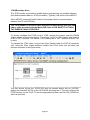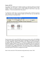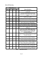
1
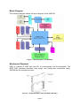
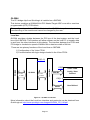
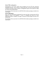
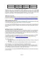
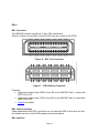
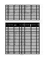
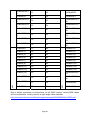
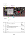
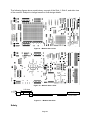
SMT498
User Manual
User Manual; Version 1.2, 11/01/05;
© Sundance Digital Signal Processing Inc. 2004
Page 1
Revision History
Changes Made
Issue
Initials
5/31/05
First release
1.0
PTM
6/1/05
Updates based on feedback
1.1
PTM
11/1/05
Update on System ACE and JTAG
1.2
SM
Page 2
List of Abbreviations
Abbreviation
Explanation
ASIC
Application Specific Integrated Circuit
BOM
Bill Of Materials
CMC
Common Mezzanine Card
Comport
Communications Port
DSP
Digital Signal Processor
FPDP
Front Panel Data Port
FPGA
Field Programmable Gate Array
NA
Not Applicable
OTP
One-Time Programmable
PC
Personal Computer
PCB
Printed Circuit Board
PCI
Peripheral Component Interconnect
PMC
PCI Mezzanine Card
PrPMC
Processor PMC
SDB
Sundance Digital Bus
SDRAM
Synchronous Dynamic Random Access Memory
SHB
Sundance High-speed Bus
SMT
Sundance Multiprocessor Technology
TBD
To Be Determined
TI
Texas Instruments
Page 3
Table of Contents
Introduction ........................................................................................................................... 7
Overview ............................................................................................................................. 7
Module Features ................................................................................................................. 7
Related Documents ............................................................................................................ 7
Block Diagram....................................................................................................................... 8
Mechanical Standard ............................................................................................................ 8
SMT498 Support.................................................................................................................... 9
SMT498 Installation .............................................................................................................. 9
QL5064 ................................................................................................................................. 10
Local bus........................................................................................................................... 10
Virtex FPGA configuration ................................................................................................ 11
Virtex FPGA design .......................................................................................................... 11
Virtex II FPGA ...................................................................................................................... 12
FPGA Block Diagram ........................................................................................................ 12
Configuration..................................................................................................................... 12
Memory ............................................................................................................................. 12
SHBs ................................................................................................................................. 13
SHB Connectors ........................................................................................................... 13
SHB Cable Assembly.................................................................................................... 14
SHB Inter Modules solutions......................................................................................... 14
Half Word Interface (16-bit SHB Interface) ................................................................... 14
RSLs ................................................................................................................................. 15
RSL Connector.............................................................................................................. 15
RSL Cable Assembly .................................................................................................... 15
Miscellaneous I/O’s ........................................................................................................... 16
System ACE SC................................................................................................................... 17
PROM ............................................................................................................................... 17
Configuration Controller .................................................................................................... 17
Flash ................................................................................................................................. 17
Power Supplies ................................................................................................................... 18
DC/DC converter............................................................................................................... 18
Linear Voltage regulator.................................................................................................... 18
Daughter Module................................................................................................................. 19
PMC Standard ..................................................................................................................... 20
Voltage keying .................................................................................................................. 20
Connectors........................................................................................................................ 20
Page 4
Component heights ........................................................................................................... 20
Board Weight .................................................................................................................... 20
Standoffs ........................................................................................................................... 20
Bezel and I/O capability .................................................................................................... 20
Power consumption .......................................................................................................... 20
Grounding ......................................................................................................................... 21
Conduction Cooling........................................................................................................... 21
Power Supply .................................................................................................................... 21
Standalone operation ........................................................................................................ 21
Only use this connector for standalone operation (i.e. when not plugged into a PCI slot)!21
Reset Structure ................................................................................................................. 21
Header Pinout...................................................................................................................... 22
PCI .................................................................................................................................... 22
SHBs ................................................................................................................................. 24
RSL Header ...................................................................................................................... 26
RSL Side 1 Pinout (LVDS only) .................................................................................... 26
RSL Side 2 Pinout (LVDS only) .................................................................................... 26
JTAG headers ................................................................................................................... 27
Power connector ............................................................................................................... 28
PCB Layout.......................................................................................................................... 28
Safety ................................................................................................................................... 29
EMC ...................................................................................................................................... 30
Appendix.............................................................................................................................. 30
Configuring the FPGA ....................................................................................................... 31
PCI Mode ...................................................................................................................... 31
JTAG/Boundary Scan ................................................................................................... 32
System ACE SC............................................................................................................ 33
Status Bit Encoding:.................................................................................................. 34
Creating System ACE programming file (.MPM)............................................................... 35
Page 5
Table of Figures
Figure 1 - Block diagram of the SMT498. ............................................................................... 8
Figure 2 – Single-Size PMC card (from IEEE 1386-2001)...................................................... 8
Figure 3 – QL5064 Connection............................................................................................. 10
Figure 4 - Default FPGA Configuration ................................................................................. 12
Figure 5 – SHB Connector.................................................................................................... 13
Figure 6 – RSL Top Connector ............................................................................................. 15
Figure 7 - RSL Bottom Connector........................................................................................ 15
Figure 8 – Location of JTAG IN, OUT and DIP Switches ..................................................... 27
Figure 9 - Module Side 1 View............................................................................................. 29
Figure 10 – Module Side 2 View ........................................................................................... 29
Figure 11 – Module Side View .............................................................................................. 29
Figure 12 - Location of the DIP Switches and the PROM ..................................................... 31
Table of Tables
Table 1 - SHB configuration Matrix ....................................................................................... 14
Table 2 – RSL Speed VS FPGA Speed Grade..................................................................... 16
Table 3 – Board Clocks......................................................................................................... 16
Table 4 – PMC P11/P12 Interface ........................................................................................ 23
Table 5 – PMC P13/P14 Interface ........................................................................................ 24
Table 6 – SHB Interface........................................................................................................ 25
Table 7 – RSL Side 1 Pinout................................................................................................. 26
Table 8 – RSL Side 2 Pinout................................................................................................. 26
Table 9 – JTAG Header Pinout............................................................................................. 27
Table 10 – Status Bits Encoding........................................................................................... 34
Page 6
Introduction
Overview
The SMT498 is Sundance’s latest FPGA PrPMC module. This module uses a Xilinx Virtex II
Pro XC2VP100, which is configured to provide two comport links, five SHB’s, two RSL’s and
other functions.
Module Features
The main features of the SMT498 are listed below:
Xilinx Virtex II Pro XC2VP100 (FF1704 package)
128MB of DDR2 SDRAM
Five SHB, two RSL, and two 8-bit Comport interfaces for easy interconnection to
Sundance products
In System Configuration using System ACE Soft Controller
Tall single-size PrPMC module
66MHz 64-bit PCI interface with over 500MB/s data rate
Related Documents
[1] PCI Mezzanine Card (PMC) Spec – IEEE.
http://shop.ieee.org/store/product.asp?prodno=SS94922
[2] Sundance High-speed Bus (SHB) specifications – Sundance.
http://sundance.com/docs/SHB%20Technical%20Specification.pdf
[3] Rocket Serial Link (RSL) specifications – Sundance.
http://sundance.com/docs/RSL%20%20Technical%20Specification%20Rev01%20Iss03.pdf
[4] Processor PMC (PrPMC) Spec – VITA.
http://www.vita.com/
[5] System ACE SC Solution Datasheet – Xilinx.
http://direct.xilinx.com/bvdocs/publications/ds088.pdf
Page 7
Block Diagram
The following diagram shows the block diagram of the SMT498.
Figure 1 - Block diagram of the SMT498.
Mechanical Standard
PMC is a variant of CMC that uses PCI to communicate over the backplane. The
IEEE CMC standard describes both single- and double-size mezzanine cards.
SMT498 will be a single-size card.
Figure 2 – Single-Size PMC card (from IEEE 1386-2001)
Page 8
Dimensions of the single-size CMC are 74.0mm wide by 149.0mm deep.
SMT498 Support
The SMT498 is supported by the SMT6041-498 software package available from
SUNDANCE. Please register on the SUNDANCE Support Forum if not yet
registered. Then enter your company’s forum and you can request the SMT6041-498
from there.
SMT498 Installation
Do NOT connect any external TTL (5v) signals to the SMT498 I/Os, which
connect directly to the FPGA, as the FPGA is NOT 5v tolerant. However the
lines on connector P14 of the carrier board are made 5V tolerant for some
applications.
You can fit the SMT498 on its own on any PMC compatible carrier board. When
mated with a carrier board such as Twin Industries Xtend1000, it may then be
plugged into a host computer (e.g. Windows PC).
Please, follow these steps to install the SMT498 module on a Host system:
1. Remove the carrier board from the host system.
2. Place the SMT498 module on a PMC site. (See your carrier board User
Manual.)Make sure that the board is firmly seated before screwing the
SMT498 to the two main mounting holes. Use 10mm M3 Standoffs (Digikey
4391K-ND) and M3 5mm bolts (Digikey H742-ND) to secure the module to
any carrier card.
3. Connect the SHB and/or RSL cables to the SMT498 (if required by your
application).
4. Install the carrier board in the host system and start the PC.
5. The SMT498 can also be used as a standalone FPGA board. Connect a
molex power connector similar to the one used for the hard disk to provide 5V.
(Note only 5V should be provided, do not provide 12 V)
Page 9
QL5064
The PCI bridge chip from QuickLogic is installed on a SMT498.
This device combines a 66MHz/64-bit PCI Master/Target ASIC core with a one-time
programmable (OTP) FPGA fabric.
The configuration of the FPGA fabric in the QL5064 is performed prior to
manufacturing of the module and cannot be changed by the user.
Local bus
QL5064 provides a bridge between the PCI bus of the host system and the Local
bus of the SMT498. This interface will allow software on the host PC to transfer data
to and from the other interfaces in this design. The interface between the FPGA and
PCI bridge is clocked at a speed of 64MHz with a data bus width of 64 bits.
There are two primary functions of the Local bus on SMT498:
1) Configuration of the Virtex FPGA
2) Communication with logic designs loaded in the Virtex FPGA
CS[3..0]
64-Bit/
66 MHz
QL5064
64-Bit/
64 MHz
Local Bus
PCI BUS
CS[0]
Virtex FPGA
8/64-Bit
Config / User
Defined
CS[3..1]
64-Bit
User Defined
Figure 3 – QL5064 Connection
More information about the Local bus interface and protocols can be obtained from
QuickLogic at: http://www.quicklogic.com/images/QL5064_CD_UM.pdf
Page 10
Virtex FPGA configuration
Programming of the Virtex FPGA can be achieved over the PCI bus using the
SelectMAP interface. This interface is 8-bits wide and runs at the full speed of the
Local bus. By simply writing a stream of configuration bytes to the location at CS[0]
the FPGA can be programmed.
An example of this is provided in the SMT6041-498 software package available from
SUNDANCE.
Virtex FPGA design
Once the FPGA has been programmed the user may then communicate with the
design by means of CS regions 1, 2 and 3. 12 address lines allow for a total
addressable space of 4kB per CS region. Accesses to these regions may be up to
64-bits wide.
An example of this is provided in the SMT6041-498 software package available from
SUNDANCE
Page 11
Virtex II FPGA
The module can be fitted with an XC2VP70 or XC2VP100 FPGA. Only flip-chip
FF1152 package will fit on this board. The choice of FPGA will be price/performance
driven.
This Xilinx Virtex II Pro, is responsible for the provision of 5 SHBs, 2 Comports via
the SHB user IO pins, a PCI Local bus interface, and 14 RSLs (see Ordering
Information).
FPGA Block Diagram
16-bit SDB
16-bit SDB
16-bit SDB
32-bit SDB
16-bit SDB
32-bit SDB
16-bit SDB
60
SHBE
SHBD
60
60
SHBB
SHBC
60
16-bit SDB
60
SHBA
Comport A
Comport
Local Bus
Interface
Comport B
Comport
QuickLogic
Figure 4 - Default FPGA Configuration
Configuration
The FPGA can be configured in three different ways:
•Loading the FPGA on power up from flash on the board using System ACE SC.
•Using the SMT6041-498 utility to load the FPGA over the PCI bus.
•Using the on-board JTAG header and Xilinx JTAG programming tools.
(See the Appendix for full details)
Memory
Two banks of DDR SDRAM are attached directly to the FPGA for storage of
incoming data. Each bank consists of two 133 MHz DDR SDRAM components
(Micron MT46V32M16FN or equivalent) providing a total of 128 MB of storage
capacity on the module.
Page 12
SHBs
SHB Connectors
The SMT498 includes five 60-pin connectors to provide SHB communication to the
outside world.
All 60 pins of each SHB connector are routed to the FPGA.
Figure 5 – SHB Connector
Features:
High-speed socket strip: QSH-030-01-L-D-A-K on the SMT498, mates with QTH030-01-L-D-A-K
QTH are used for cable assembly or PCB connecting 2 PMCs.
Centreline: 0.5mm (0.0197”) QSH Connector
An adapter is available for Agilent probes for the 16760A Logic Analyser.
The 2 probes supported are the E5378A 100-pin Single-ended Probe and the
E5386A Half Channel Adapter with E5378A.
The SMT498 can include five Sundance High-speed Bus (SHB) interfaces, three on
PMC Side 1 and two on PMC Side 2. They are connected directly to the FPGA
device, and can support data rates of 100MHz.
Two of the SHBs on Side 1 are wired to support LVDS. Each of these connectors
can support 28 pairs of LVDS data including 1 pair for clock input. Due to a lack of
clock inputs on the FPGA, only SHBA fully supports 2x16-bit SDB mode. All SHBs
fully support 32-bit mode. See Table 1 for details.
SHB
16-bit SDB
capable?
32-bit SDB
capable?
LVDS capable?
A
2xTX/RX
TX/RX
No
B
2xTX, 1xRX
TX/RX
TX/RX
C
2xTX, 1xRX
TX/RX
No
Page 13
D
2xTX, 1xRX
TX/RX
No
E
2xTX, 1xRX
TX/RX
TX/RX
Table 1 - SHB configuration Matrix
The demo logic will configure SHBA, SHBB, SHBE as receivers, while SHBC and
SHBD are transmitters. As SHBA is the only SHB that can support two 16-bit SDB
receivers, it will be configured for that implementation. The rest of the SHBs either
support 32-bit SDBs or 16-bit SDB transmitters. See Figure 4 for details.
SHB Cable Assembly
The cable is custom made by Precision Interconnect and a cable assembly solution
builder can be found at: http://www.precisionint.com/tdibrsb/content/howtouse.asp
SHB Inter Modules solutions
High-speed data transfer can be achieved between PMC modules thanks to the use
of a 60-way flat ribbon micro-coax cable or via PCB connections.
As a result, NO DIFFERENTIAL lines are required to transfer data on long distances
and at speeds in excess of 100MHz, which allows the full use of the SHB connector
60 pins.
Half Word Interface (16-bit SHB Interface)
The SHB connectors provide connections to the external world. You can implement
your own interface to transfer data over using these connectors, but if you want to
communicate with other Sundance modules, you can implement a Half Word (Hw)
interface sitting on 25 pins of an SHB connector.
The SHBs are parallel communication links for synchronous transmission. An SHB
interface is derived from the SDB interface which is a 16-bit wide synchronous
communication interface. (SUNDANCE SDB specification)
The differences are:
• The SHB interface can be made Byte (8 bits), Half Word (16 bits) or Word (32
bits) wide.
• The transfer rate can be increased thanks to better quality interconnect.
As an example, let us consider the Half Word (Hw) SHB interface.
You can implement 2 x 16-bit SHB interfaces per SHB connector, and have some
spare signals for User defined functions. (no differential lines are needed thanks to
our SHB cable assembly described in SHB Cable Assembly).
You must refer to the latest SUNDANCE SDB specification for technical information
on how it works.
Page 14
RSLs
RSL Connector
The SMT498 includes two 28-pin (7-pair) RSL connectors.
28 pins (7 pairs) of each RSL connector (52 total) are routed to the FPGA
Figure 6 – RSL Top Connector
Figure 7 - RSL Bottom Connector
Features:
• High-speed socket strip: QSE-014-xx-DP on the SMT407 Side 1, mates with
QTE-014-xx-DP
• High-speed socket strip: QTE-014-xx-DP on the SMT407 Side 2, mates with
QSE-014-xx-DP
• Samtec for details.
RSL Cable Assembly
Cable assemblies with QTE connectors on one side and QSE on the other are like
the flexible versions of the PCB adapters mentioned above.
RSL Interface
Page 15
The RSL connectors are the fastest FPGA connections available on SMT498.
As RSL are based on RocketIO transceiver blocks, the speed is limited by the speed
grade of FPGA installed:
Table 2 – RSL Speed VS FPGA Speed Grade
Based on the above, the 14 bi-directional links of SMT498 can provide a combined
bandwidth of up to 37.5Gbps.
Refer to the latest SUNDANCE RSL specification for technical information on how it
works.
Local bus
http://www.quicklogic.com/images/QL5064_CD_UM.pdf
Clocks
The FPGA is provided with the following clocks:
Description Speed
QL5064 Local bus clock
64MHz
SHB clock
100MHz
RSL LVDS clock
125MHz
Table 3 – Board Clocks
Miscellaneous I/O’s
The following external interfaces will be provided for user-defined functions:
•
PMC P14 (64-bits 5V tolerant)
•
4 LEDs
•
4 DIP switches
Page 16
System ACE SC
The SMT498 FPGA PMC module is equipped with In System FPGA configuration
solution called System ACE SC. As soon as the board is powered up the FPGA is
configured from the flash. The System ACE SC has a PROM, Configuration
controller, and a Flash. For more information on System ACE look at: System ACE
PROM
The System ACE SC solution has a OTP PROM XC17V01. The PROM is
programmed with the configuration controller before it is installed on the board.
Configuration Controller
The XCV50E is used as the configuration controller. The PROM on power up
configures the Virtex-E chip (XCV50E). After configuration the XCV50E is seen as a
XCCACE64M (System ACE chip) in the JTAG chain. The controller forms a link
between the Flash and the target FPGA. Four status LEDs are connected to the
controller to monitor its state. (See the Appendix for status bit encoding table).
Flash
A 8MB Flash ROM device is connected to the XCV50E configuration controller. The
target FPGA bitstream is loaded in to this Flash via JTAG to configure the FPGA on
power up.
Page 17
Power Supplies
Due to the close packing of components between PMC Side 1 and the host module,
power consumption is limited to 4.0W for 10.0mm standoffs (this increases to 6.0W
for 13.0mm standoffs). The total consumption for Side 1 and Side 2 of the module
shall not exceed 7.5W, and represents the total power drawn from all power rails
provided at the connector (+5V, +3.3v, +VI/O, +12V,-12V, +3.3Vaux).
For this reason it is recommended that you analyse the total FPGA device power
drawn by using Xilinx XPOWER before implementing your design in the FPGA.
This module must have 5V and 3.3V supplied through the PMC connectors. Either
5V or 3.3V may be supplied for PCI I/O voltage and should be consistent with the
signaling standard of the PCI host bus. +12V and -12V are optional and may be
supplied to the PMC connectors as per PMC specifications.
Contained on the module are linear regulators for the FPGA VCCAUX and FPGA
RocketIO. A DC/DC converter supplies the core voltage for the FPGA and DSPs.
DC/DC converter
An International Rectifier IP1201 Power Block is used to supply the 1.5V core
voltage to the FPGA. The current limits are configured for 10A and 5A, respectively.
The DC/DC converter is powered from the 5V supply.
Linear Voltage regulator
The FPGA VCCAUX and FPGA RocketIO voltages are supplied through linear
voltage regulators drawn from 3.3V.
Page 18
Daughter Module
SMT498 has been designed to incorporate the option for a daughter module that can
interface to the FPGA and provide external I/O functions. SMT498 has one location
for a daughter module. The daughter module interfaces to SMT498 via SHBE,
therefore this SHB will not be available when the daughter module is installed.
Page 19
PMC Standard
Voltage keying
The QuickLogic 5064 bridge is both 3.3V and 5V compliant. Both keying holes are
provided.
Connectors
According to IEEE 1386.1-2001 connectors Pn1 through Pn3 are provided for 64-bit
PCI connectivity. Additionally, connector Pn4 is provided for 64 bits of user-defined
I/O. Given that SMT498 is a single-size card, these connectors are referenced from
P11 through P14.
Component heights
This module obeys the PrPMC Tall module specs for component heights. Heights of
components on PMC Side 1 (see Figure 10) are limited to 4.7mm except in the I/O
Area (where they may extend to the host module surface). Components on PMC
Side 2 (see Figure 10) are limited to 23.5mm minus PCB thickness, or about
22.0mm (assuming 1.5mm PCB thickness).
Board Weight
The SMT498 weighs approximately 85 grams
Standoffs
There are two standoffs as part of the module. The standoffs are of standard 10mm
height in order to support the broadest range of host modules.
Bezel and I/O capability
Access to the right-angle FPDP port is provided through the front panel. For
purposes of mechanical rigidity and EMC compliance a customised bezel is provided
through which the FPDP is accessed.
Power consumption
Due to the close packing of components between PMC Side 1 and the host module,
power consumption is limited to 4.0W for 10.0mm standoffs (this increases to 6.0W
for 13.0mm standoffs). For Tall PrPMC modules an additional cooling method such
as a heat sink and fan should be considered if the total module power exceeds 25W.
Page 20
The following information shall be provided on the PMC card:
5V current drawn, peak and average
3.3V current drawn, peak and average
Note: While it may appear that a stacking height of 13.0mm is desirable, some hosts
may not accept this.
Grounding
Per section 4.14 of IEEE 1386-2001.
Conduction Cooling
As the SMT498 adheres to PrPMC standards, the entire active and hot parts are on
the back of the module, which is suitable to place a conduction plate at the back of
the module to provide conduction coolong.
Power Supply
The SMT498 shall conform to the PMC standard for single-size modules. The PCI
connectors supply the module with 5.0V and 3.3V power supply. The 3.3V will be
used to supply all LVTTL digital I/O voltages directly. The FPGA Core Voltage
(VCCINT = 1.5V) is generated from the 5.0V. FPGA Auxiliary voltage (VCCAUX = 2.5V) is
derived from 3.3V to minimise losses.
Note: Due to restrictions of the Virtex II Pro, the FPGA Auxiliary voltage (VCCAUX)
must be provided before VCCO (3.3V). Given that VCCO is generated externally and
VCCAUX is generated locally, there will need to be a means to switch VCCO built into the
hardware.
Standalone operation
A 4-pin 0.200” power connector such as the type used to power PC hard disks will
be provided on Side 2 of the module. This connector provides 5V, 12V power, and
ground. SMT498 will generate 3.3V on board from the 5V supply.
Only use this connector for standalone operation (i.e. when not plugged into a
PCI slot)!
Reset Structure
The SMT498 shall obey the reset signal provided by the PCI connector. In the
absence of an external reset signal, the module will bring itself out of reset once all
supplies are in compliance.
Page 21
Header Pinout
PCI
A 66MHz 64-bit PCI bridge will allow SMT498 to communicate with the host system.
As the Local Bus has a maximum clock speed of 64MHz, the maximum theoretical
speed data can be transferred between the host and FPGA is 512MB/s.
PMC PCI connectors are directly connected to the QuickLogic 5064 bridge chip.
PMC P14 must be 5V tolerant.
P11
P12
Pin # Signal name Signal name Pin # Pin # Signal name
Signal name Pin #
1 TCK
-12V
2
1 +12V
TRSTN
2
3 GND
INTAN
4
3 TMS
TDO
4
5 INTBN
INTCN
6
5 TDI
GND
6
8
7 GND
PCI-RSVD*
8
9 PCI-RSVD*
PCI-RSVD*
10
7 BUSMODE1 +5V
N
9 INTDN
PCI-RSVD*
10
11 GND
3.3Vaux
12
11 BUSMODE2N +3.3V
12
13 CLK
GND
14
13 RSTN
BUSMODE3
N
14
15 GND
GNTN
16
15 +3.3V
BUSMODE4
N
16
17 REQN
+5V
18
17 PMEN
GND
18
19 VIO
AD31
20
19 AD30
AD29
20
21 AD28
AD27
22
21 GND
AD26
22
23 AD25
GND
24
23 AD24
+3.3V
24
25 GND
C/BE3N
26
25 IDSEL
AD23
26
27 AD22
AD21
28
27 +3.3V
AD20
28
29 AD19
+5V
30
29 AD18
GND
30
31 VIO
AD17
32
31 AD16
C/BE2N
32
33 FRAMEN
GND
34
33 GND
PMC-RSVD
34
35 GND
IRDYN
36
35 TRDYN
+3.3V
36
37 DEVSELN
+5V
38
37 GND
STOPN
38
39 GND
LOCKN
40
39 PERRN
GND
40
41 PCI-RSVD*
PCI-RSVD*
42
41 +3.3V
SERRN
42
43 PAR
GND
44
43 C/BE1N
GND
44
Page 22
45 VIO
AD15
46
45 AD14
AD13
46
47 AD12
AD11
48
47 M66EN
AD10
48
49 AD9
+5V
50
49 AD8
+3.3V
50
51 GND
C/BE0N
52
51 AD7
PMC-RSVD
52
53 AD6
AD5
54
53 +3.3V
PMC-RSVD
54
55 AD4
GND
56
55 PMC-RSVD
GND
56
57 VIO
AD3
58
57 PMC-RSVD
PMC-RSVD
58
59 AD2
AD1
60
59 GND
PMC-RSVD
60
61 AD0
+5V
62
61 ACK64N
+3.3V
62
63 GND
REQ64N
64
63 GND
PMC-RSVD
64
Table 4 – PMC P11/P12 Interface
P13
Pin # Signal name Signal
name
P14
Pin # Pin # Signal name
Signal name Pin #
1 PCI-RSVD
GND
2
1 I/O
I/O
2
3 GND
C/BE7N
4
3 I/O
I/O
4
5 C/BE6N
C/BE5N
6
5 I/O
I/O
6
7 C/BE4N
GND
8
7 I/O
I/O
8
9 VIO
PAR64
10
9 I/O
I/O
10
11 AD63
AD62
12
11 I/O
I/O
12
13 AD61
GND
14
13 I/O
I/O
14
15 GND
AD60
16
15 I/O
I/O
16
17 AD59
AD58
18
17 I/O
I/O
18
19 AD57
GND
20
19 I/O
I/O
20
21 VIO
AD56
22
21 I/O
I/O
22
23 AD55
AD54
24
23 I/O
I/O
24
25 AD53
GND
26
25 I/O
I/O
26
27 GND
AD52
28
27 I/O
I/O
28
29 AD51
AD50
30
29 I/O
I/O
30
31 AD49
GND
32
31 I/O
I/O
32
33 GND
AD48
34
33 I/O
I/O
34
35 AD47
AD46
36
35 I/O
I/O
36
37 AD45
GND
38
37 I/O
I/O
38
Page 23
39 VIO
AD44
40
39 I/O
I/O
40
41 AD43
AD42
42
41 I/O
I/O
42
43 AD41
GND
44
43 I/O
I/O
44
45 GND
AD40
46
45 I/O
I/O
46
47 AD39
AD38
48
47 I/O
I/O
48
49 AD37
GND
50
49 I/O
I/O
50
51 GND
AD36
52
51 I/O
I/O
52
53 AD35
AD34
54
53 I/O
I/O
54
55 AD33
GND
56
55 I/O
I/O
56
57 VIO
AD32
58
57 I/O
I/O
58
59 PCI-RSVD
PCI-RSVD
60
59 I/O
I/O
60
61 PCI-RSVD
GND
62
61 I/O
I/O
62
63 GND
PCI-RSVD
64
62 I/O
I/O
64
Table 5 – PMC P13/P14 Interface
SHBs
The SHB signals have been named to match 2 16-bit SDB interfaces (or Hw SHB
interface) pinout according to the SUNDANCE SHB specification Half Word
configuration. SMT498 will be equipped with 4 SHBs. Two SHBs will be wired to the
FPGA to support LVDS.
QSH Pin
number
QSH Pin
number
Hw
SHBxCLK0
1
2
SHBxD0(0)
SHBxD0(1)
3
4
SHBxD0(2)
SHBxD0(3)
5
6
SHBxD0(4)
SHBxD0(5)
7
8
SHBxD0(6)
SHBxD0(7)
9
10
SHBxD0(8)
SHBxD0(9)
11
12
SHBxD0(10)
SHBxD0(11)
13
14
SHBxD0(12)
SHBxD0(13)
15
16
SHBxD0(14)
SHBxD0(15)
17
18
SHBxUSER0(1
6)
SHBxUSER0(1
7)
19
20
SHBxUSER0(1
8)
Page 24
Hw0
Hw0
Hw
21
22
SHBxWEN1
SHBxREQ1
23
24
SHBxACK1
SHBxUSER1(2
3)
25
26
SHBxUSER1(2
4)
SHBxUSER1(2
5)
27
28
SHBxUSER1(2
6)
SHBxUSER1(2
7)
29
30
SHBxUSER1(2
8)
SHBxUSER1(2
9)
31
32
SHBxUSER1(3
0)
SHBxUSER1(3
1)
33
34
SHBxUSER1(3
2)
SHBxUSER1(3
3)
35
36
SHBxUSER1(3
4)
SHBxCLK3
37
38
SHBxD1(0)
SHBxD1(1)
39
40
SHBxD1(2)
SHBxD1(3)
41
42
SHBxD1(4)
SHBxD1(5)
43
44
SHBxD1(6)
SHBxD1(7)
45
46
SHBxD1(8)
SHBxD1(9)
47
48
SHBxD1(10)
SHBxD1(11)
49
50
SHBxD1(12)
SHBxD1(13)
51
52
SHBxD1(14)
SHBxD1(15)
53
54
SHBxUSER2(5
2)
SHBxUSER2(5
3)
55
56
SHBxUSER2(5
4)
SHBxUSER2(5
5)
57
58
SHBxWEN4
SHBxREQ4
59
60
Hw1
Hw1
SHBxUSER0(1
9)
SHBxACK4
Table 6 – SHB Interface
Due to height constraints of components on the PMC module, vertical SHB cables
will not be possible. Luckily, there is a right-angle cable available:
http://www.precisionint.com/tdibrsb/images/drawings/D043850NNNLLLDD20.pdf
Page 25
RSL Header
Headers are per RSL Spec.
RSL Side 1 Pinout (LVDS only)
Table 7 – RSL Side 1 Pinout
RSL Side 2 Pinout (LVDS only)
Table 8 – RSL Side 2 Pinout
Page 26
JTAG headers
The JTAG header is used to access the XC2VP FPGA scan chain and configure the System
ACE configuration solution.
RSL Connectors
SHB Connectors
JTAG IN
DIP Switch S2
JTAG OUT
Figure 8 – Location of JTAG IN, OUT and DIP Switches
The JTAG/Multilinx header has the following pinout:
Table 9 – JTAG Header Pinout
Page 27
A JTAG In port and JTAG Out port are provided for chaining multiple modules
together. A DIP switch is provided to activate the JTAG Out port.
Power connector
A power connector is provided on the board for stand-alone operation. This
connector is a 4-pin male header similar to the type used to power PC hard disk
drives. Although the standard pinout for these connectors provides 5V and 12V
power; only 5V will be required to power the module.
PCB Layout
Page 28
The following figures show a preliminary concept of the Side 1, Side 2, and side view
of the module. Subject to change based on final design details.
Figure 9 - Module Side 1 View
Figure 10 – Module Side 2 View
10
mm
I/ O Area
FPDP
PCI Connx
SHB
SHB
FPGA
Figure 11 – Module Side View
Safety
Page 29
QL 5064
PCB Plane
This module presents no hazard to the user.
EMC
This module is designed to operate from within an enclosed host system, which is
build to provide EMC shielding. Operation within the EU EMC guidelines is not
guaranteed unless it is installed within an adequate host system.
Appendix
Page 30
Configuring the FPGA
The module will be provided with the default VHDL core burned in the Flash. On
power up, the FPGA will be configured with the default bitstream. In case the user
wants to use his own custom design the following method can be used to configure
the FPGA.
It is assumed that the user is familiar with Xtend1000 PMC carrier card and is aware
of the procedure for mounting the PMC on the Xtend1000 and powering it up within a
PC environment.
PCI Mode
To configure the FPGA (Virtex II Pro – VP 100) using the PCI interface, switchswitch 4 of S3 to ‘ON’ position and use the PCI driver for SMT407/498 to download
the firmware to the FPGA.
PROM (there is a
S3
jumper near this PROM
which is not shown in this picture)
Figure 12 - Location of the DIP Switches and the PROM
Page 31
S2
JTAG/Boundary Scan
The JTAG header is provided to enable device programming via suitable software.
(See board header table for JTAG pin details). Typically, this will be Xilinx iMPACT.
Xilinx iMPACT supports Parallel Cable IV download cable for communication
between the PC and FPGA(s).
The JTAG header on the board was designed to mate directly with the 2mm
ribbon cable provided with the MultiLINX Cable IV. BE SURE TO ATTACH
THE RIBBON CABLE PROPERLY.
To directly configure the FPGA via the JTAG, remove the jumper near the PROM
chip as shown on the picture below. Turn switch 1 of S2 to ‘ON’ position and switch 2
of S2 to ‘OFF’ position. The switch 4 of S3 should be in ‘OFF’ position for the JTAG
to work.
To initialize the JTAG chain, connect the Xilinx Parallel cable to JTAG IN connector
JA2. Using the Xilinx impact software initialize the JTAG chain, this will show two
devices as shown in the figure below
The first device will be the XC2VP100 and the second device will be XCV50E.
Assign the intended .BIT file to the XC2VP100 and program it. This will configure the
FPGA directly via the JTAG. To test the approaches please use the LED_FLASH.bit,
which is provided.
Page 32
System ACE SC
To configure the FPGA from the Flash on power up, install the jumper pin near the
PROM chip. Turn the switch 1 of S2 to ‘ON’ position and switch 2 of S2 to ‘OFF’
position. Switch 4 of S3 should be in ‘OFF’ position for the JTAG to work and
switches 1, 2, and 3 should be in the ‘ON’ position.
To initialize the JTAG chain, connect the Xilinx Parallel cable to JTAG IN connector
JA2. Using the Xilinx impact software initialize the JTAG chain, this will show two
devices as shown in the figure below
The first device will be the XC2VP100 and the second device will be XCCACEM64
SC (this is the System ACE chip that allows the bitstream to be loaded into the flash
via JTAG). Assign the .MPM file (Generation of the .MPM file is given at the end) to
the System ACE chip and program it. To check the configuration of the VP100 via
the Flash, toggle the switch 4 of S3 this will reset the system ACE and configure the
FPGA from the Flash. You will see the done pin (LED D5, which is not populated on
the prototype) of the Target FPGA go low. This confirms the FPGA is configured and
you will see the status LED’s D12, D13 lit. From now onwards as soon as the board
is powered up the VP100 will be configured from Flash.
Note: In this mode the VP100 cannot be configured directly via the JTAG.
Page 33
Status Bit Encoding:
Status bits (3..0)
D14
D13
D12
D11
Status Definition
1
1
1
1
System busy. Cannot process JTAG
commands
1
1
1
0
Successful slave-serial or select map
configuration (CFG_DONE High). System
Busy.
1
1
0
1
Configuration Error (CFG_DONE did not go
high). System Busy.
1
1
0
0
Decompressor error. System Busy.
1
0
1
1
Invalid controller state. System Buy.
1
0
1
0
Flash memory blank or invalid configuration
data in Flash memory. System Busy.
1
0
0
1
Invalid configuration option. System Busy.
1
0
0
0
Flash Chip erase successful. System Busy.
0
1
1
1
System ready to accept commands through
JTAG port.
0
1
1
0
Successful Slave-serial/ Slave Select
MAP configuration (CFG_DONE high).
System ready to accept commands
through JTAG port.
0
1
0
1
Configuration Error (CFG_DONE did not go
high). System ready to accept commands
through JTAG port.
0
1
0
0
Decompressor error. System ready to
accept commands through JTAG port.
0
0
1
1
Invalid controller state. System ready to
accept commands through JTAG port.
0
0
1
0
Flash memory blank or invalid configuration
data in Flash memory. System ready to
accept commands through JTAG port.
0
0
0
1
Invalid configuration option. System ready to
accept commands through JTAG port.
0
0
0
0
Flash Chip erase successful. System ready
to accept commands through JTAG port.
Table 10 – Status Bits Encoding
Page 34
Creating System ACE programming file (.MPM)
Once the .BIT file is generated using the normal procedure open Xilinx iMPACT
software. Under mode select ‘File mode’. In the blank space right click to launch
wizard.
a) Select ‘System ACE MPM/SC’. Click Next.
Page 35
b) Select size as 64Mbits as the flash can hold 64Mbits.
c) Specify the name of the .MPM file and the location to store it.
Page 36
d) Select ‘In Select MAP mode’.
e) Select ‘CS0’ as there is only one Target FPGA on the board
Page 37
f) Select ‘Configuration Addr 0’. Click Next. If multiple bitstreams are stored
under different configuration addresses. The bitstream select switches must
be set to the particular address before the board is powered up, in order to
configure the target FPGA with the respective bitstream.
g) Click Next
h) Add the respective .BIT file, with which you intend to configure the target
FPGA.
Page 38
i) Click on Finish.
j) Click on Yes to Generate file.
k) Do not compress the file. Click OK.
Once the file is generated, it will be stored in the location specified.
Page 39