1
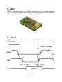
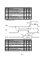
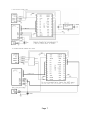
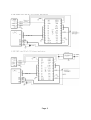
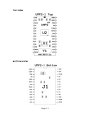
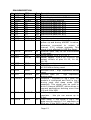
UMP2
USB to 8-bit Parallel FIFO
Interface Module
User’s Manual
CONTENTS
1. UMP2.........................................................................................3
2. USAGE........................................................................................3
FIFO read cycle....................................................................... 3
FIFO write cycle...................................................................... 4
3. FEATURES..................................................................................6
4. TYPICAL UMP2 APPLICATION SCHEMATICS.............................. 6
USB CONNECTOR:................................................................... 6
5. TECHNICAL REFERENCE...........................................................10
UMP2 INTERNAL SCHEMATICS ................................................ 10
TOP VIEW............................................................................. 11
BOTTOM VIEW...................................................................... 11
PIN DESCRIPTION................................................................. 12
6. DRIVER INSTALATION.............................................................13
7. TECHNICAL SPECIFICATION....................................................13
ABSOLUTE RATINGS.............................................................. 13
TYPICAL RATINGS.................................................................. 14
8. CONTACT................................................................................. 14
Page 2
1. UMP2
UMP2 is a module based on FT245BM integrated circuit manufactured by
FTDI Ltd., which provides with easy to use USB connectivity to PC without
any need of additional knowledge about USB itself.
2. USAGE
UMP2 is a USB to 8-bit bidirectional parallel FIFO interface with simple
flow control.
FIFO read cycle
Page 3
Time Description
Min
Max Unit
T1
RD Active Pulse Width
50
ns
T2
RD to RD Pre-Charge Time
50
ns
T3
RD Active to Valid Data
T4
Valid Data Hold Time from RD 10
inactive
T5
RD Inactive to RXF#
5
T6
RXF inactive after RD cycle
80
30
ns
ns
25
ns
ns
FIFO write cycle
Time Description
Min
T7
WR Active Pulse Width
50
ns
T8
WR to WR Pre-Charge Time
50
ns
T9
Data Setup
inactive
T10
Data Hold Time from WR inactive 10
T11
WR Inactive to TXE#
5
T12
TXE inactive after RD cycle
80
Time
before
WR
Page 4
Max Unit
20
ns
ns
25
ns
ns
The module is capable of data transfer rates up to 1 MB/sec using direct
driver and up to 3 MBd using virtual COM port driver. In addition there is
an EEPROM memory which may be used to store VID and PID identifiers
for OEM applications.
The module connects by 2 signals directly to USB connector, while the
application side provides 8 bidirectional signals plus flow control.
From mechanical standpoint, the module is arranged as DIP28 with
standard pin spacing of 0.1 inch (2.54 mm) so it is possible to fit it into
either common or precise DIP28 socket, or to solder it directly to printed
circuit board. The USB connector is to be connected externally which
allows the designer to choose the placement of the connector and its type:
'B' or 'mini B' or USB cable soldered directly to the board may be used.
This design sigificantly simplifies the development in small production
series.
There is a separate power supply for IO pins (VCCIO), which allows the
module to be connected to 3.0 V application easily.
The data transfer can be optimized by SI/WU signal which controls two
functions: In suspend mode (PWREN#=1), if there is "Remote WakeUp"
option in EEPROM turned on, falling edge will wake up the device.
In normal operation, falling edge will force immediate data transfer to PC
regardless of the amount of data in the buffer, otherwise the data is
typically being sent in 64 byte blocks.
PWREN# signal is designated to drive a P-channel MOSFET for applications
which drain more than 100 mA (max. 500 mA) from USB. In such case it
is advisable to turn on 'enable pull-down' option in EEPROM configuration.
Module UMP2 can also operate in "BitBang mode", in which the data pins
act as 8-bit parallel input/output. This mode can be used for example
to configure field-programmable logic array directly from PC over USB.
Further, there is RSTOUT# signal, which stays in high impedance state for
about 2 ms after power up and then it is connected to internal 3.3 V
voltage regulator. Signal RSTOUT# is also in high inpedance state
whenever signal RESET# is active (RESET#=log.0), but it is not affected
by reset from USB (USB Bus RESET).
The module is equipped with 93LC56 memory of 128×16 bits. Lower half
of this memory is used for module's needs (64×16 bits). Using EEDATA,
EESK and EECS the application may use upper 64×16 bits for its own
purposes. While the application is accessing module's EEPROM memory,
the RESET# signal must be active (RESET#=log.0).
Software drivers fow Windows 98/ME/2K/XP/CE, Mac OS8/OS9/OS X and
Linux are available for free on FTDI website (http://www.ftdichip.com/).
Page 5
3. FEATURES
•
•
•
•
•
•
•
•
•
•
•
•
•
Data inputs/outputs 3.0 to 5 V - CMOS compatible
Powered from USB or external supply
Data transfer rates up to 1 MB/sec with direct driver and up to 3 MBd
with virtual COM port driver
Hardware flow control
384 byte receive buffer
128 byte transmit buffer
Supports USB 1.1 protocol, USB 2.0 compatible
BitBang mode, which allows the module to be used as 8-bit
bidirectional I/O (signals RD#/WR/TXE#/RXF# are not used in this
mode)
PWREN# signal for driving P-channel MOSFET for applications draining
more than 100 mA from USB (max. 500 mA)
Support for OEM application (VID and PID are stored in EEPROM
memory which is part of the module)
Ability to use use free EEPROM capacity (64×16 bits)
Drivers for Windows 98/2K/ME/XP, Mac OS8/OS9/OS X and Linux
available for free
DIP28 socket compatible, PCB mountable
4. TYPICAL UMP2 APPLICATION SCHEMATICS
USB CONNECTOR:
Page 6
Page 7
Page 8
Page 9
5. TECHNICAL REFERENCE
UMP2 INTERNAL SCHEMATICS
Page 10
TOP VIEW
BOTTOM VIEW
Page 11
PIN DESCRIPTION
Pin
1
2
3
4
5
6
7
8
9
10
11
12
13
Label
GND
VCC
SIWU
D7
D6
D5
D4
D3
D2
D1
D0
GND
RSO#
FTDI
GND
VCC
SI/WU
D7
D6
D5
D4
D3
D2
D1
D0
GND
RSTOUT#
Typ
PWR
PWR
IN
I/O
I/O
I/O
I/O
I/O
I/O
I/O
I/O
PWR
OUT
14 RST#
RESET#
IN
15 VCC
16 VIO
VCC
VCCIO
PWR
PWR
17 GND
18 ECS
GND
EECS
PWR
I/O
19 ESK
EESK
OUT
20 EDT
EEDATA
I/O
21 PWRE#
PWREN#
OUT
22 3V3
3V3OUT
OUT
23 RXF#
RXF#
OUT
Description
Signal ground
Power supply +4.4 V to 5.25 V
Send immediate/WakeUp
Bidirectional data bus, bit 7
Bidirectional data bus, bit 6
Bidirectional data bus, bit 5
Bidirectional data bus, bit 4
Bidirectional data bus, bit 3
Bidirectional data bus, bit 2
Bidirectional data bus, bit 1
Bidirectional data bus, bit 0
Signal ground
High impedance for about 2 ms after
power up and during #RESET is active,
otherwise connected to output of
internal 3.3 V voltage regulator. This
signal is not affected by USB Bus Reset.
External reset. May be left unconnected
if not used.
Power supply +4.4 V to 5.25 V.
Power supply +3.0 V to +5.25 V for
output drivers of pins 10..12, 14..16,
18..25.
Signal ground
EEPROM enable – internal pull-up
of 200 kOhm during reset.
EEPROM clock - high impedance during
reset.
EEPROM data I/O - high impedance
during reset.
PWREN# - switched to log.0 after the
module is configured and held in log.1
during reset and sleep mode (USB
suspend). This signal may be used to
drive P-channel MOSFET, which allows to
connect applications draining more than
100 mA from USB.
3.3 V output
from
internal
voltage
regulator - this pin can source up to
5 mA.
Data ready, if this signal is log.0, the
data may be read by 1-0-1 sequence on
RD# pin. If the RXF# signal is log.1, the
Page 12
24 TXE#
TXE#
IN
25 WR
WR
IN
26 RD#
RD#
IN
27 USBDP
USBDP
I/O
28 USBDM
USBDM
I/O
data is invalid.
Transmit enabled, if this signal is log.0
the data may be written by 0-1-0
sequence on WR pin. If the TXE# signal
is log.1, the buffer if full.
Write signal – falling edge of this signal
writes data to FTDI buffer.
Read data – falling edge of this signal
causes 1 byte of data to be read from
FTDI buffer and sent to data pins.
USB data signal plus. It is necessary to
connect resistor of 1.5 kOhm between
USBDP and 3V3OUT or RSTOUT#.
USB data signal minus.
6. DRIVER INSTALATION
For Windows operating systems there are two types of drivers:
•
Virtual COM port, which can be accessed as common COM port using
Win32 API
• Direct driver, to gain full control of the chip, a DLL to interface the
driver is provided
Detailed description of driver installation procedure can be found on FTDI
website (http://www.ftdichip.com/).
7. TECHNICAL SPECIFICATION
ABSOLUTE RATINGS
Storage temperature
TSTR
min. -65 °C
max. 150 °C
Operational temperature
TPWR
min. 0 °C
max. 70 °C
Power supply voltage
VCCMAX
min. -0.5 V
max. 6.00 V
Input voltage – inputs
VIN1
min. -0.5 V
max. VCC+0.5 V
Input voltage - I/O
VIN2
min. -0.5 V
max. VCC+0.5 V
Output current – outputs
IO1
max. 24 mA
Output current - I/O
IO2
max. 24 mA
Power
WPWR
max. 500 mW
Page 13
TYPICAL RATINGS
VCC Operating supply
voltage
Operating supply current
Suspended supply current
Input voltage log.1
Input voltage log.0
Output voltage log.1
VCC
Output voltage log.0
VOL
Output current log.1
IOH
Input current log.0
IOL
ICC1
ICC2
VIH
VIL
VOH
min. 4.4 V
max. 5.25 V
max. 50 mA
max. 250 µA
min. 2.0 V
max. 1.0 V
min. 2.8 V,
Ri=15 kOhm
max. 0.3 V,
Ri=1.5 kOhm
4 mA,
VOH=VCC-0.5 V
8 mA,
VOL=0.5 V
8. CONTACT
Address:
ASIX s.r.o.
Staropramenna 4
150 00 Prague
Czech Republic
E-Mail:
[email protected] (general information)
[email protected] (sales inquiries, ordering)
[email protected] (technical support)
WWW:
www.asix-tools.com (development tools)
www.asix.info (company website)
Tel.:
+420-257 312 378
Fax:
+420-257 329 116
UMP2_EN.PDF
Copyright © 1991-2007 ASIX s.r.o.
All trademarks used in this document are properties of their respective owners. This
information is provided in the hope that it will be useful, but without any warranty. We
disclaim any liability for the accuracy of this information. We are not responsible for the
contents of web pages referenced by this document.
Page 14