1
TMS320C54x DSP
Reference Set
Volume 1: CPU and Peripherals
Literature Number: SPRU131G
March 2001
Printed on Recycled Paper
IMPORTANT NOTICE
Texas Instruments and its subsidiaries (TI) reserve the right to make changes to their products
or to discontinue any product or service without notice, and advise customers to obtain the latest
version of relevant information to verify, before placing orders, that information being relied on
is current and complete. All products are sold subject to the terms and conditions of sale supplied
at the time of order acknowledgment, including those pertaining to warranty, patent infringement,
and limitation of liability.
TI warrants performance of its products to the specifications applicable at the time of sale in
accordance with TI’s standard warranty. Testing and other quality control techniques are utilized
to the extent TI deems necessary to support this warranty. Specific testing of all parameters of
each device is not necessarily performed, except those mandated by government requirements.
Customers are responsible for their applications using TI components.
In order to minimize risks associated with the customer’s applications, adequate design and
operating safeguards must be provided by the customer to minimize inherent or procedural
hazards.
TI assumes no liability for applications assistance or customer product design. TI does not
warrant or represent that any license, either express or implied, is granted under any patent right,
copyright, mask work right, or other intellectual property right of TI covering or relating to any
combination, machine, or process in which such products or services might be or are used. TI’s
publication of information regarding any third party’s products or services does not constitute TI’s
approval, license, warranty or endorsement thereof.
Reproduction of information in TI data books or data sheets is permissible only if reproduction
is without alteration and is accompanied by all associated warranties, conditions, limitations and
notices. Representation or reproduction of this information with alteration voids all warranties
provided for an associated TI product or service, is an unfair and deceptive business practice,
and TI is not responsible nor liable for any such use.
Resale of TI’s products or services with statements different from or beyond the parameters stated
by TI for that products or service voids all express and any implied warranties for the associated
TI product or service, is an unfair and deceptive business practice, and TI is not responsible nor
liable for any such use.
Also see: Standard Terms and Conditions of Sale for Semiconductor Products.
www.ti.com/sc/docs/stdterms.htm
Mailing Address:
Texas Instruments
Post Office Box 655303
Dallas, Texas 75265
Copyright 2001, Texas Instruments Incorporated
Preface
Read This First
About This Manual
The TMS320C54x DSP is a fixed-point digital signal processor (DSP) in the
TMS320 DSP family. This book serves as a reference for the C54x DSP
and provides information for developing hardware and software applications
using the C54x DSP.
This user’s guide contains limited information about the enhanced peripherals
available on some C54x devices. For detailed information on the enhanced
peripherals, see TMS320C54x DSP Enhanced Peripherals Reference Guide,
literature number SPRU302.
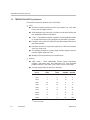
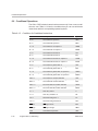
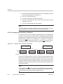
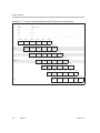
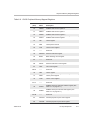
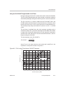
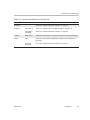
How to Use This Manual
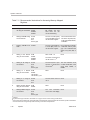
The following table summarizes the TMS320C54x DSP information contained
in this book.
If you are looking for
information about:
Turn to these chapters:
Addressing modes
Chapter 5, Data Addressing
Chapter 6, Program Memory Addressing
Buffered serial port
Chapter 9, Serial Ports
Bus structure
Chapter 2, Architectural Overview
Clock generator
Chapter 2, Architectural Overview
Chapter 8, On-Chip Peripherals
CPU architecture
Chapter 2, Architectural Overview
Chapter 4, Central Processing Unit
SPRU131G
External bus
Chapter 10, External Bus Operation
Hold mode
Chapter 10, External Bus Operation
Host port interface
Chapter 8, On-Chip Peripherals
iii
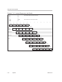
How to Use This Manual
If you are looking for
information about:
Turn to these chapters:
Interrupts
Chapter 6, Program Memory Addressing
Memory
Chapter 2, Architectural Overview
Chapter 3, Memory
On-chip peripherals
Chapter 8, On-Chip Peripherals
Overview of the C54x
Chapter 1, Introduction
Parallel I/O Ports
Chapter 2, Architectural Overview
Chapter 8, On-Chip Peripherals
Power-down modes
Chapter 6, Program Memory Addressing
Program control
Chapter 6, Program Memory Addressing
Pipeline latencies
Chapter 7, Pipeline
Reset
Chapter 6, Program Memory Addressing
ROM code submission to TI
Appendix C, Submitting ROM Codes to TI
Serial ports
Chapter 9, Serial Ports
Status registers
Chapter 4, Central Processing Unit
TDM serial port
Chapter 9, Serial Ports
Timer
Chapter 2, Architectural Overview
Chapter 8, On-Chip Peripherals
Wait-state generator
Chapter 2, Architectural Overview
Chapter 8, On-Chip Peripherals
iv
Read This First
SPRU131G
Notational
Conventions
Notational Conventions / Information
About
Cautions
Notational Conventions
This book uses the following conventions.
- The TMS320C54x DSP can use either of two forms of the instruction set:
a mnemonic form or an algebraic form. This book uses the mnemonic form
of the instruction set. For information about the mnemonic form of the
instruction set, see TMS320C54x DSP Reference Set, Volume 2:
Mnemonic Instruction Set, literature number SPRU172. For information
about the algebraic form of the instruction set, see TMS320C54x DSP
Reference Set, Volume 3: Algebraic Instruction Set, literature number
SPRU179.
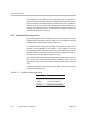
- Program listings and program examples are shown in a special type-
face.
Here is a segment of a program listing:
STL
RSBX
B
A,*AR1+
INTM
MAIN_PG
;Int_RAM(I)=0
;Globally enable interrupts
;Return to foreground program
- Square brackets, [ and ], identify an optional parameter. If you use an
optional parameter, specify the information within the brackets; do not type
the brackets themselves.
Information About Cautions
This book contains cautions.
This is an example of a caution statement.
A caution statement describes a situation that could potentially
damage your software or equipment.
The information in a caution is provided for your protection. Please read each
caution carefully.
SPRU131G
Read This First
v
Related Documentation from Texas Instruments
Related Documentation from Texas Instruments
The following books describe the TMS320C54x DSP and related support
tools. To obtain a copy of any of these TI documents, call the Texas Instruments Literature Response Center at (800) 477-8924. When ordering, please
identify the book by its title and literature number. Many of these documents
are located on the internet at http://www.ti.com.
TMS320C54x DSP Reference Set, Volume 1: CPU (literature number
SPRU131) describes the TMS320C54x 16-bit fixed-point
general-purpose digital signal processors. Covered are its architecture,
internal register structure, data and program addressing, and the
instruction pipeline. Also includes development support information,
parts lists, and design considerations for using the XDS510 emulator.
TMS320C54x DSP Reference Set, Volume 2: Mnemonic Instruction Set
(literature number SPRU172) describes the TMS320C54x digital
signal processor mnemonic instructions individually. Also includes a
summary of instruction set classes and cycles.
TMS320C54x DSP Reference Set, Volume 3: Algebraic Instruction Set
(literature number SPRU179) describes the TMS320C54x digital
signal processor algebraic instructions individually. Also includes a
summary of instruction set classes and cycles.
TMS320C54x DSP Reference Set, Volume 4: Applications Guide
(literature number SPRU173) describes software and hardware
applications for the TMS320C54x digital signal processor. Also
includes development support information, parts lists, and design
considerations for using the XDS510 emulator.
TMS320C54x DSP Reference Set, Volume 5: Enhanced Peripherals
(literature number SPRU302) describes the enhanced peripherals available on the TMS320C54x digital signal processors. Includes the multichannel buffered serial ports (McBSPs), direct memory access (DMA)
controller, interprocessor communications, and the HPI-8 and HPI-16
host port interfaces.
TMS320C54x DSP Family Functional Overview (literature number
SPRU307) provides a functional overview of the devices included in the
TMS320C54x DSP generation of digital signal processors. Included
are descriptions of the CPU architecture, bus structure, memory structure, on-chip peripherals, and instruction set.
vi
Read This First
SPRU131G
Related Documentation from Texas Instruments
TMS320C54x DSKplus User’s Guide (literature number SPRU191)
describes the TMS320C54x digital signal processor starter kit (DSK),
which allows you to execute custom TMS320C54x DSP code in real time
and debug it line by line. Covered are installation procedures, a
description of the debugger and the assembler, customized applications,
and initialization routines.
TMS320C54x Code Composer Studio Tutorial (literature number
SPRU327) introduces the Code Composer Studio integrated development environment and software tools for the TMS320C54x.
Code Composer User’s Guide (literature number SPRU328) explains how to
use the Code Composer development environment to build and debug
embedded real-time DSP applications.
TMS320C54x Assembly Language Tools User’s Guide (literature number
SPRU102) describes the assembly language tools (assembler, linker,
and other tools used to develop assembly language code), assembler
directives, macros, common object file format, and symbolic debugging
directives for the TMS320C54x generation of devices.
TMS320C54x Optimizing C Compiler User’s Guide (literature number
SPRU103) describes the TMS320C54x C compiler. This C compiler
accepts ANSI standard C source code and produces assembly language
source code for the TMS320C54x generation of devices.
TMS320C54x Simulator Getting Started (literature number SPRU137)
describes how to install the TMS320C54x simulator and the C source
debugger for the TMS320C54x DSP. The installation for MS-DOS,
PC-DOS, SunOS, Solaris, and HP-UX systems is covered.
TMS320C54x Evaluation Module Technical Reference (literature number
SPRU135) describes the TMS320C54x evaluation module, its
features, design details and external interfaces.
TMS320C54x Code Generation Tools Getting Started Guide (literature
number SPRU147) describes how to install the TMS320C54x
assembly language tools and the C compiler for the TMS320C54x
devices. The installation for MS-DOS, OS/2, SunOS, Solaris, and
HP-UX 9.0x systems is covered.
TMS320C5xx C Source Debugger User’s Guide (literature number
SPRU099) tells you how to invoke the TMS320C54x emulator,
evaluation module, and simulator versions of the C source debugger
interface. This book discusses various aspects of the debugger
interface, including window management, command entry, code
execution, data management, and breakpoints. It also includes a tutorial
that introduces basic debugger functionality.
SPRU131G
Read This First
vii
Technical
Articles
Related Documentation
from Texas Instruments / Technical Articles
TMS320C54x Simulator Addendum (literature number SPRU170) tells you
how to define and use a memory map to simulate ports for the
TMS320C54x DSP. This addendum to the TMS320C5xx C Source
Debugger User’s Guide discusses standard serial ports, buffered serial
ports, and time division multiplexed (TDM) serial ports.
Setting Up TMS320 DSP Interrupts in C Application Report (literature
number SPRA036) describes methods of setting up interrupts for the
TMS320 DSP family of processors in C programming language.
Sample code segments are provided, along with complete examples of
how to set up interrupt vectors.
TMS320VC5402 and TMS320UC5402 Bootloader (literature number
SPRA618) describes the features and operation of the TMS320VC5402
and TMS320UC5402 bootloader. Also discussed is the contents of the
on-chip ROM.
TMS320C548/C549 Bootloader Technical Reference (literature number
SPRU288) describes the process the bootloader uses to transfer user
code from an external source to the program memory at power up. (Presently available only on the internet.)
TMS320 Third-Party Support Reference Guide (literature number
SPRU052) alphabetically lists over 100 third parties that provide various
products that serve the TMS320 DSP family. A myriad of products and
applications are offered—software and hardware development tools,
speech recognition, image processing, noise cancellation, modems, etc.
Technical Articles
A wide variety of related documentation is available on digital signal processing.
These references fall into one of the following application categories:
viii
Read This First
General-Purpose DSP
Graphics/Imagery
Speech/Voice
Control
Multimedia
Military
Telecommunications
Automotive
Consumer
Medical
Development Support
SPRU131G
Technical Articles
In the following list, references appear in alphabetical order according to
author. The documents contain beneficial information regarding designs, operations, and applications for signal-processing systems; all of the documents
provide additional references. Texas Instruments strongly suggests that you
refer to these publications.
General-Purpose DSP:
1) Chassaing, R., Horning, D.W., “Digital Signal Processing with Fixed and
Floating-Point Processors” , CoED, USA, Volume 1, Number 1, pages 1-4,
March 1991.
2) Defatta, David J., Joseph G. Lucas, and William S. Hodgkiss, Digital Signal Processing: A System Design Approach, New York: John Wiley, 1988.
3) Erskine, C., and S. Magar, “Architecture and Applications of a SecondGeneration Digital Signal Processor,” Proceedings of IEEE International
Conference on Acoustics, Speech, and Signal Processing, USA, 1985.
4) Essig, D., C. Erskine, E. Caudel, and S. Magar, “A Second-Generation
Digital Signal Processor,” IEEE Journal of Solid-State Circuits, USA, Volume SC-21, Number 1, pages 86-91, February 1986.
5) Frantz, G., K. Lin, J. Reimer, and J. Bradley, “The Texas Instruments
TMS320C25 Digital Signal Microcomputer,” IEEE Microelectronics, USA,
Volume 6, Number 6, pages 10-28, December 1986.
6) Gass, W., R. Tarrant, T. Richard, B. Pawate, M. Gammel, P. Rajasekaran,
R. Wiggins, and C. Covington, “Multiple Digital Signal Processor Environment for Intelligent Signal Processing,” Proceedings of the IEEE, USA,
Volume 75, Number 9, pages 1246-1259, September 1987.
7) Jackson, Leland B., Digital Filters and Signal Processing, Hingham, MA:
Kluwer Academic Publishers, 1986.
8) Jones, D.L., and T.W. Parks, A Digital Signal Processing Laboratory Using
the TMS32010, Englewood Cliffs, NJ: Prentice-Hall, Inc., 1987.
9) Lim, Jae, and Alan V. Oppenheim, Advanced Topics in Signal Processing,
Englewood Cliffs, NJ: Prentice- Hall, Inc., 1988.
10) Lin, K., G. Frantz, and R. Simar, Jr., “The TMS320 Family of Digital Signal
Processors,” Proceedings of the IEEE, USA, Volume 75, Number 9, pages
1143-1159, September 1987.
11) Lovrich, A., Reimer, J., “An Advanced Audio Signal Processor” , Digest of
Technical Papers for 1991 International Conference on Consumer Electronics, June 1991.
SPRU131G
Read This First
ix
Technical Articles
12) Magar, S., D. Essig, E. Caudel, S. Marshall and R. Peters, “An NMOS Digital Signal Processor with Multiprocessing Capability,” Digest of IEEE International Solid-State Circuits Conference, USA, February 1985.
13) Oppenheim, Alan V., and R.W. Schafer, Digital Signal Processing, Englewood Cliffs, NJ: Prentice-Hall, Inc., 1975 and 1988.
14) Papamichalis, P.E., and C.S. Burrus, “Conversion of Digit-Reversed to BitReversed Order in FFT Algorithms,” Proceedings of ICASSP 89, USA,
pages 984-987, May 1989.
15) Papamichalis, P., and R. Simar, Jr., “The TMS320C30 Floating-Point Digital Signal Processor,” IEEE Micro Magazine, USA, pages 13-29, December 1988.
16) Papamichalis, P.E., “FFT Implementation on the TMS320C30,” Proceedings of ICASSP 88, USA, Volume D, page 1399, April 1988.
17) Parks, T.W., and C.S. Burrus, Digital Filter Design, New York, NY: John Wiley
and Sons, Inc., 1987.
18) Peterson, C., Zervakis, M., Shehadeh, N., “Adaptive Filter Design and
Implementation Using the TMS320C25 Microprocessor” , Computers in
Education Journal, USA, Volume 3, Number 3, pages 12-16, July-September 1993.
19) Prado, J., and R. Alcantara, “A Fast Square-Rooting Algorithm Using a
Digital Signal Processor,” Proceedings of IEEE, USA, Volume 75, Number
2, pages 262-264, February 1987.
20) Rabiner, L.R. and B. Gold, Theory and Applications of Digital Signal Processing, Englewood Cliffs, NJ: Prentice-Hall, Inc., 1975.
21) Simar, Jr., R., and A. Davis, “The Application of High-Level Languages to
Single-Chip Digital Signal Processors,” Proceedings of ICASSP 88, USA,
Volume D, page 1678, April 1988.
22) Simar, Jr., R., T. Leigh, P. Koeppen, J. Leach, J. Potts, and D. Blalock, “A
40 MFLOPS Digital Signal Processor: the First Supercomputer on a Chip,”
Proceedings of ICASSP 87, USA, Catalog Number 87CH2396-0, Volume 1,
pages 535-538, April 1987.
23) Simar, Jr., R., and J. Reimer, “The TMS320C25: a 100 ns CMOS VLSI Digital Signal Processor,” 1986 Workshop on Applications of Signal Processing
to Audio and Acoustics, September 1986.
24) Texas Instruments, Digital Signal Processing Applications with the TMS320
Family, 1986; Englewood Cliffs, NJ: Prentice-Hall, Inc., 1987.
25) Treichler, J.R., C.R. Johnson, Jr., and M.G. Larimore, A Practical Guide
to Adaptive Filter Design, New York, NY: John Wiley and Sons, Inc., 1987.
x
Read This First
SPRU131G
Technical Articles
Graphics/Imagery:
1) Reimer, J., and A. Lovrich, “Graphics with the TMS32020,” WESCON/85
Conference Record, USA, 1985.
Speech/Voice:
1) DellaMorte, J., and P. Papamichalis, “Full-Duplex Real-Time Implementation of the FED-STD-1015 LPC-10e Standard V.52 on the TMS320C25,”
Proceedings of SPEECH TECH 89, pages 218-221, May 1989.
2) Gray, A.H., and J.D. Markel, Linear Prediction of Speech, New York, NY:
Springer-Verlag, 1976.
3) Frantz, G.A., and K.S. Lin, “A Low-Cost Speech System Using the
TMS320C17,” Proceedings of SPEECH TECH ’87, pages 25-29, April
1987.
4) Papamichalis, P., and D. Lively, “Implementation of the DOD Standard
LPC-10/52E on the TMS320C25,” Proceedings of SPEECH TECH ’87,
pages 201-204, April 1987.
5) Papamichalis, Panos, Practical Approaches to Speech Coding, Englewood Cliffs, NJ: Prentice-Hall, Inc., 1987.
6) Pawate, B.I., and G.R. Doddington, “Implementation of a Hidden Markov
Model-Based Layered Grammar Recognizer,” Proceedings of ICASSP
89, USA, pages 801- 804, May 1989.
7) Rabiner, L.R., and R.W. Schafer, Digital Processing of Speech Signals,
Englewood Cliffs, NJ: Prentice-Hall, Inc., 1978.
8) Reimer, J.B. and K.S. Lin, “TMS320 Digital Signal Processors in Speech
Applications,” Proceedings of SPEECH TECH ’88, April 1988.
9) Reimer, J.B., M.L. McMahan, and W.W. Anderson, “Speech Recognition
for a Low-Cost System Using a DSP,” Digest of Technical Papers for 1987
International Conference on Consumer Electronics, June 1987.
Control:
1) Ahmed, I., “16-Bit DSP Microcontroller Fits Motion Control System Application,” PCIM, October 1988.
2) Ahmed, I., “Implementation of Self Tuning Regulators with TMS320 Family
of Digital Signal Processors,” MOTORCON ’88, pages 248-262, September 1988.
3) Allen, C. and P. Pillay, “TMS320 Design for Vector and Current Control of
AC Motor Drives” , Electronics Letters, UK, Volume 28, Number 23, pages
2188-2190, November 1992.
SPRU131G
Read This First
xi
Technical Articles
4) Panahi, I. and R. Restle, “DSPs Redefine Motion Control” , Motion Control
Magazine, December 1993.
5) Lovrich, A., G. Troullinos, and R. Chirayil, “An All-Digital Automatic Gain
Control,” Proceedings of ICASSP 88, USA, Volume D, page 1734, April
1988.
6) Ahmed, I., and S. Meshkat, “Using DSPs in Control,” Control Engineering,
February 1988.
7) Meshkat, S., and I. Ahmed, “Using DSPs in AC Induction Motor Drives,”
Control Engineering, February 1988.
8) Matsui, N. and M. Shigyo, “Brushless DC Motor Control Without Position
and Speed Sensors” , IEEE Transactions on Industry Applications, USA,
Volume 28, Number 1, Part 1, pages 120-127, January-February 1992.
9) Hanselman, H., “LQG-Control of a Highly Resonant Disc Drive Head Positioning Actuator,” IEEE Transactions on Industrial Electronics, USA, Volume 35, Number 1, pages 100-104, February 1988.
10) Bose, B.K., and P.M. Szczesny, “A Microcomputer-Based Control and
Simulation of an Advanced IPM Synchronous Machine Drive System for
Electric Vehicle Propulsion,” Proceedings of IECON ’87, Volume 1, pages
454-463, November 1987.
11) Ahmed, I., and S. Lindquist, “Digital Signal Processors: Simplifying HighPerformance Control,” Machine Design, September 1987.
Multimedia:
1) Reimer, J., “DSP-Based Multimedia Solutions Lead Way Enhancing
Audio Compression Performance” , Dr. Dobbs Journal, December 1993.
2) Reimer, J., G. Benbassat, and W. Bonneau Jr., “Application Processors:
Making PC Multimedia Happen” , Silicon Valley PC Design Conference,
July 1991.
Military:
1) Papamichalis, P., and J. Reimer, “Implementation of the Data Encryption
Standard Using the TMS32010,” Digital Signal Processing Applications,
1986.
Telecommunications:
1) Ahmed, I., and A. Lovrich, “Adaptive Line Enhancer Using the
TMS320C25,” Conference Records of Northcon/86, USA, 14/3/1-10,
September/October 1986.
xii
Read This First
SPRU131G
Technical Articles
2) Casale, S., R. Russo, and G. Bellina, “Optimal Architectural Solution Using DSP Processors for the Implementation of an ADPCM Transcoder,”
Proceedings of GLOBECOM ’89, pages 1267-1273, November 1989.
3) Cole, C., A. Haoui, and P. Winship, “A High-Performance Digital Voice
Echo Canceller on a SINGLE TMS32020,” Proceedings of ICASSP 86,
USA, Catalog Number 86CH2243-4, Volume 1, pages 429-432, April
1986.
4) Cole, C., A. Haoui, and P. Winship, “A High-Performance Digital Voice
Echo Canceller on a Single TMS32020,” Proceedings of IEEE International Conference on Acoustics, Speech and Signal Processing, USA, 1986.
5) Lovrich, A., and J. Reimer, “A Multi-Rate Transcoder,” Transactions on
Consumer Electronics, USA, November 1989.
6) Lovrich, A. and J. Reimer, “A Multi-Rate Transcoder” , Digest of Technical
Papers for 1989 International Conference on Consumer Electronics, June 7-9,
1989.
7) Lu, H., D. Hedberg, and B. Fraenkel, “Implementation of High-Speed Voiceband Data Modems Using the TMS320C25,” Proceedings of ICASSP 87,
USA, Catalog Number 87CH2396-0, Volume 4, pages 1915-1918, April
1987.
8) Mock, P., “Add DTMF Generation and Decoding to DSP- µP Designs,”
Electronic Design, USA, Volume 30, Number 6, pages 205-213, March
1985.
9) Reimer, J., M. McMahan, and M. Arjmand, “ADPCM on a TMS320 DSP
Chip,” Proceedings of SPEECH TECH 85, pages 246-249, April 1985.
10) Troullinos, G., and J. Bradley, “Split-Band Modem Implementation Using the
TMS32010 Digital Signal Processor,” Conference Records of Electro/86 and
Mini/Micro Northeast, USA, 14/1/1-21, May 1986.
Automotive:
1) Lin, K., “Trends of Digital Signal Processing in Automotive,” International
Congress on Transportation Electronic (CONVERGENCE ’88), October
1988.
Consumer:
1) Frantz, G.A., J.B. Reimer, and R.A. Wotiz, “Julie, The Application of DSP
to a Product,” Speech Tech Magazine, USA, September 1988.
2) Reimer, J.B., and G.A. Frantz, “Customization of a DSP Integrated Circuit
for a Customer Product,” Transactions on Consumer Electronics, USA,
August 1988.
SPRU131G
Read This First
xiii
Technical
Technical Articles
Articles / Trademarks
3) Reimer, J.B., P.E. Nixon, E.B. Boles, and G.A. Frantz, “Audio Customization of a DSP IC,” Digest of Technical Papers for 1988 International Conference on Consumer Electronics, June 8-10 1988.
Medical:
1) Knapp and Townshend, “A Real-Time Digital Signal Processing System
for an Auditory Prosthesis,” Proceedings of ICASSP 88, USA, Volume A,
page 2493, April 1988.
2) Morris, L.R., and P.B. Barszczewski, “Design and Evolution of a PocketSized DSP Speech Processing System for a Cochlear Implant and Other
Hearing Prosthesis Applications,” Proceedings of ICASSP 88, USA, Volume A, page 2516, April 1988.
Development Support:
1) Mersereau, R., R. Schafer, T. Barnwell, and D. Smith, “A Digital Filter Design
Package for PCs and TMS320,” MIDCON/84 Electronic Show and Convention, USA, 1984.
2) Simar, Jr., R., and A. Davis, “The Application of High-Level Languages to
Single-Chip Digital Signal Processors,” Proceedings of ICASSP 88, USA,
Volume 3, pages 1678-1681, April 1988.
Trademarks
TMS320, TMS320C2x, TMS320C20x, TMS320C24x, TMS320C5x,
TMS320C54x, C54x, 320 Hotline On-line, Micro Star, TI, XDS510, and
XDS510WS are trademarks of Texas Instruments.
HP-UX is a trademark of Hewlett-Packard Company.
MS-DOS and Windows are trademarks of Microsoft Corporation.
OS/2 and PC-DOS are trademarks of International Business Machines
Corporation.
PAL is a registered trademark of Advanced Micro Devices, Inc.
Solaris and SunOS are trademarks of Sun Microsystems, Inc.
SPARC is a trademark of SPARC International, Inc., but licensed exclusively
to Sun Microsystems, Inc.
xiv
Read This First
SPRU131G
Contents
Contents
1
2
Introduction . . . . . . . . . . . . . . . . . . . . . . . . . . . . . . . . . . . . . . . . . . . . . . . . . . . . . . . . . . . . . . . . . . . . .
Summarizes the features of the TMS320 family of products and presents typical applications.
Describes the TMS320C54x DSP and lists its key features.
1.1
TMS320 DSP Family Overview . . . . . . . . . . . . . . . . . . . . . . . . . . . . . . . . . . . . . . . . . . . . . . .
1.1.1 History, Development, and Advantages of TMS320 DSPs . . . . . . . . . . . . . . . . .
1.1.2 Typical Applications for the TMS320 DSP Family . . . . . . . . . . . . . . . . . . . . . . . .
1.2
TMS320C54x DSP Overview . . . . . . . . . . . . . . . . . . . . . . . . . . . . . . . . . . . . . . . . . . . . . . . . .
1.3
TMS320C54x DSP Key Features . . . . . . . . . . . . . . . . . . . . . . . . . . . . . . . . . . . . . . . . . . . . .
1-1
1-2
1-2
1-3
1-5
1-6
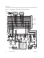
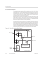
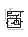
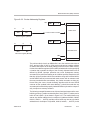
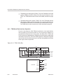
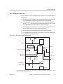
Architectural Overview . . . . . . . . . . . . . . . . . . . . . . . . . . . . . . . . . . . . . . . . . . . . . . . . . . . . . . . . . . 2-1
Summarizes the TMS320C54x DSP architecture. Provides general information about the CPU,
bus structures, internal memory organization, on-chip peripherals, and scanning logic.
2.1
Bus Structure . . . . . . . . . . . . . . . . . . . . . . . . . . . . . . . . . . . . . . . . . . . . . . . . . . . . . . . . . . . . . . 2-3
2.2
Internal Memory Organization . . . . . . . . . . . . . . . . . . . . . . . . . . . . . . . . . . . . . . . . . . . . . . . . 2-5
2.2.1 On-Chip ROM . . . . . . . . . . . . . . . . . . . . . . . . . . . . . . . . . . . . . . . . . . . . . . . . . . . . . . . 2-5
2.2.2 On-Chip Dual-Access RAM (DARAM) . . . . . . . . . . . . . . . . . . . . . . . . . . . . . . . . . . 2-6
2.2.3 On-Chip Single-Access RAM (SARAM) . . . . . . . . . . . . . . . . . . . . . . . . . . . . . . . . . 2-6
2.2.4 On-Chip Two-Way Shared RAM . . . . . . . . . . . . . . . . . . . . . . . . . . . . . . . . . . . . . . . 2-6
2.2.5 On-Chip Memory Security . . . . . . . . . . . . . . . . . . . . . . . . . . . . . . . . . . . . . . . . . . . . 2-6
2.2.6 Memory-Mapped Registers . . . . . . . . . . . . . . . . . . . . . . . . . . . . . . . . . . . . . . . . . . . 2-7
2.3
Central Processing Unit (CPU) . . . . . . . . . . . . . . . . . . . . . . . . . . . . . . . . . . . . . . . . . . . . . . . 2-8
2.3.1 Arithmetic Logic Unit (ALU) . . . . . . . . . . . . . . . . . . . . . . . . . . . . . . . . . . . . . . . . . . . 2-8
2.3.2 Accumulators . . . . . . . . . . . . . . . . . . . . . . . . . . . . . . . . . . . . . . . . . . . . . . . . . . . . . . . 2-8
2.3.3 Barrel Shifter . . . . . . . . . . . . . . . . . . . . . . . . . . . . . . . . . . . . . . . . . . . . . . . . . . . . . . . . 2-9
2.3.4 Multiplier/Adder Unit . . . . . . . . . . . . . . . . . . . . . . . . . . . . . . . . . . . . . . . . . . . . . . . . . 2-9
2.3.5 Compare, Select, and Store Unit (CSSU) . . . . . . . . . . . . . . . . . . . . . . . . . . . . . . 2-10
2.4
Data Addressing . . . . . . . . . . . . . . . . . . . . . . . . . . . . . . . . . . . . . . . . . . . . . . . . . . . . . . . . . . . 2-10
2.5
Program Memory Addressing . . . . . . . . . . . . . . . . . . . . . . . . . . . . . . . . . . . . . . . . . . . . . . . 2-11
2.6
Pipeline Operation . . . . . . . . . . . . . . . . . . . . . . . . . . . . . . . . . . . . . . . . . . . . . . . . . . . . . . . . . 2-11
2.7
On-Chip Peripherals . . . . . . . . . . . . . . . . . . . . . . . . . . . . . . . . . . . . . . . . . . . . . . . . . . . . . . . 2-12
2.7.1 General-Purpose I/O Pins . . . . . . . . . . . . . . . . . . . . . . . . . . . . . . . . . . . . . . . . . . . 2-12
2.7.2 Software-Programmable Wait-State Generator . . . . . . . . . . . . . . . . . . . . . . . . . 2-13
2.7.3 Programmable Bank-Switching Logic . . . . . . . . . . . . . . . . . . . . . . . . . . . . . . . . . 2-13
2.7.4 Hardware Timer . . . . . . . . . . . . . . . . . . . . . . . . . . . . . . . . . . . . . . . . . . . . . . . . . . . . 2-13
2.7.5 Clock Generator . . . . . . . . . . . . . . . . . . . . . . . . . . . . . . . . . . . . . . . . . . . . . . . . . . . . 2-13
2.7.6 Direct Memory Access (DMA) Controller . . . . . . . . . . . . . . . . . . . . . . . . . . . . . . . 2-14
2.7.7 Host Port Interface . . . . . . . . . . . . . . . . . . . . . . . . . . . . . . . . . . . . . . . . . . . . . . . . . . 2-14
xv
Contents
2.8
2.9
2.10
3
3.3
3.4
3.5
Memory Space . . . . . . . . . . . . . . . . . . . . . . . . . . . . . . . . . . . . . . . . . . . . . . . . . . . . . . . . . . . . . 3-2
Program Memory . . . . . . . . . . . . . . . . . . . . . . . . . . . . . . . . . . . . . . . . . . . . . . . . . . . . . . . . . . 3-15
3.2.1 Program Memory Configurability . . . . . . . . . . . . . . . . . . . . . . . . . . . . . . . . . . . . . 3-16
3.2.2 On-Chip ROM Organization . . . . . . . . . . . . . . . . . . . . . . . . . . . . . . . . . . . . . . . . . . 3-17
3.2.3 Program Memory Address Map and On-Chip ROM Contents . . . . . . . . . . . . . 3-18
3.2.4 On-Chip ROM Code Contents and Mapping . . . . . . . . . . . . . . . . . . . . . . . . . . . 3-18
3.2.5 Extended Program Memory (Available on C548/549/5402/5410/5420) . . . . . 3-20
Data Memory . . . . . . . . . . . . . . . . . . . . . . . . . . . . . . . . . . . . . . . . . . . . . . . . . . . . . . . . . . . . . 3-22
3.3.1 Data Memory Configurability . . . . . . . . . . . . . . . . . . . . . . . . . . . . . . . . . . . . . . . . . 3-22
3.3.2 On-Chip RAM Organization . . . . . . . . . . . . . . . . . . . . . . . . . . . . . . . . . . . . . . . . . . 3-23
3.3.3 Memory-Mapped Registers . . . . . . . . . . . . . . . . . . . . . . . . . . . . . . . . . . . . . . . . . . 3-25
3.3.4 CPU Memory-Mapped Registers . . . . . . . . . . . . . . . . . . . . . . . . . . . . . . . . . . . . . 3-26
I/O Memory . . . . . . . . . . . . . . . . . . . . . . . . . . . . . . . . . . . . . . . . . . . . . . . . . . . . . . . . . . . . . . . 3-29
Program and Data Security . . . . . . . . . . . . . . . . . . . . . . . . . . . . . . . . . . . . . . . . . . . . . . . . . 3-30
Central Processing Unit . . . . . . . . . . . . . . . . . . . . . . . . . . . . . . . . . . . . . . . . . . . . . . . . . . . . . . . . . . 4-1
Describes the TMS320C54x CPU operations. Includes information about the arithmetic logic
unit, the accumulators, the shifter, the multiplier/adder unit, the compare, select, store unit, and
the exponent encoder.
4.1
4.2
4.3
xvi
2-15
2-15
2-15
2-16
2-16
2-17
2-17
Memory . . . . . . . . . . . . . . . . . . . . . . . . . . . . . . . . . . . . . . . . . . . . . . . . . . . . . . . . . . . . . . . . . . . . . . . . . 3-1
Describes the TMS320C54x DSP memory configuration and operation. Includes memory
maps and descriptions of program memory, data memory, and I/O space. Also includes
descriptions of the CPU memory-mapped registers.
3.1
3.2
4
Serial Ports . . . . . . . . . . . . . . . . . . . . . . . . . . . . . . . . . . . . . . . . . . . . . . . . . . . . . . . . . . . . . . .
2.8.1 Synchronous Serial Ports . . . . . . . . . . . . . . . . . . . . . . . . . . . . . . . . . . . . . . . . . . . .
2.8.2 Buffered Serial Ports . . . . . . . . . . . . . . . . . . . . . . . . . . . . . . . . . . . . . . . . . . . . . . . .
2.8.3 Multichannel Buffered Serial Ports (McBSPs) . . . . . . . . . . . . . . . . . . . . . . . . . .
2.8.4 TDM Serial Ports . . . . . . . . . . . . . . . . . . . . . . . . . . . . . . . . . . . . . . . . . . . . . . . . . . .
External Bus Interface . . . . . . . . . . . . . . . . . . . . . . . . . . . . . . . . . . . . . . . . . . . . . . . . . . . . . .
IEEE Standard 1149.1 Scanning Logic . . . . . . . . . . . . . . . . . . . . . . . . . . . . . . . . . . . . . . .
CPU Status and Control Registers . . . . . . . . . . . . . . . . . . . . . . . . . . . . . . . . . . . . . . . . . . . . 4-2
4.1.1 Status Registers (ST0 and ST1) . . . . . . . . . . . . . . . . . . . . . . . . . . . . . . . . . . . . . . . 4-2
4.1.2 Processor Mode Status Register (PMST) . . . . . . . . . . . . . . . . . . . . . . . . . . . . . . . 4-6
Arithmetic Logic Unit (ALU) . . . . . . . . . . . . . . . . . . . . . . . . . . . . . . . . . . . . . . . . . . . . . . . . . 4-10
4.2.1 ALU Input . . . . . . . . . . . . . . . . . . . . . . . . . . . . . . . . . . . . . . . . . . . . . . . . . . . . . . . . . 4-10
4.2.2 Overflow Handling . . . . . . . . . . . . . . . . . . . . . . . . . . . . . . . . . . . . . . . . . . . . . . . . . . 4-11
4.2.3 The Carry Bit . . . . . . . . . . . . . . . . . . . . . . . . . . . . . . . . . . . . . . . . . . . . . . . . . . . . . . 4-12
4.2.4 Dual 16-Bit Mode . . . . . . . . . . . . . . . . . . . . . . . . . . . . . . . . . . . . . . . . . . . . . . . . . . . 4-12
Accumulators A and B . . . . . . . . . . . . . . . . . . . . . . . . . . . . . . . . . . . . . . . . . . . . . . . . . . . . . . 4-13
4.3.1 Storing Accumulator Contents . . . . . . . . . . . . . . . . . . . . . . . . . . . . . . . . . . . . . . . . 4-13
4.3.2 Accumulator Shift and Rotate Operations . . . . . . . . . . . . . . . . . . . . . . . . . . . . . . 4-14
4.3.3 Saturation Upon Accumulator Store . . . . . . . . . . . . . . . . . . . . . . . . . . . . . . . . . . . 4-15
4.3.4 Application-Specific Instructions . . . . . . . . . . . . . . . . . . . . . . . . . . . . . . . . . . . . . . 4-15
Contents
SPRU131G
Contents
4.4
4.5
4.6
4.7
5
4-17
4-19
4-20
4-22
4-23
4-24
4-27
Data Addressing . . . . . . . . . . . . . . . . . . . . . . . . . . . . . . . . . . . . . . . . . . . . . . . . . . . . . . . . . . . . . . . . . 5-1
Describes the seven basic addressing modes of the TMS320C54x DSP.
5.1
5.2
5.3
5.4
5.5
5.6
5.7
5.8
6
Barrel Shifter . . . . . . . . . . . . . . . . . . . . . . . . . . . . . . . . . . . . . . . . . . . . . . . . . . . . . . . . . . . . . .
Multiplier/Adder Unit . . . . . . . . . . . . . . . . . . . . . . . . . . . . . . . . . . . . . . . . . . . . . . . . . . . . . . .
4.5.1 Multiplier Input Sources . . . . . . . . . . . . . . . . . . . . . . . . . . . . . . . . . . . . . . . . . . . . .
4.5.2 Multiply/Accumulate (MAC) Instructions . . . . . . . . . . . . . . . . . . . . . . . . . . . . . . .
4.5.3 MAC and MAS Saturation Upon Multiplication . . . . . . . . . . . . . . . . . . . . . . . . . .
Compare, Select, and Store Unit (CSSU) . . . . . . . . . . . . . . . . . . . . . . . . . . . . . . . . . . . . .
Exponent Encoder . . . . . . . . . . . . . . . . . . . . . . . . . . . . . . . . . . . . . . . . . . . . . . . . . . . . . . . . .
Immediate Addressing . . . . . . . . . . . . . . . . . . . . . . . . . . . . . . . . . . . . . . . . . . . . . . . . . . . . . . 5-2
Absolute Addressing . . . . . . . . . . . . . . . . . . . . . . . . . . . . . . . . . . . . . . . . . . . . . . . . . . . . . . . . 5-4
5.2.1 dmad Addressing . . . . . . . . . . . . . . . . . . . . . . . . . . . . . . . . . . . . . . . . . . . . . . . . . . . . 5-4
5.2.2 pmad Addressing . . . . . . . . . . . . . . . . . . . . . . . . . . . . . . . . . . . . . . . . . . . . . . . . . . . . 5-5
5.2.3 PA Addressing . . . . . . . . . . . . . . . . . . . . . . . . . . . . . . . . . . . . . . . . . . . . . . . . . . . . . . 5-5
5.2.4 *(lk) Addressing . . . . . . . . . . . . . . . . . . . . . . . . . . . . . . . . . . . . . . . . . . . . . . . . . . . . . 5-5
Accumulator Addressing . . . . . . . . . . . . . . . . . . . . . . . . . . . . . . . . . . . . . . . . . . . . . . . . . . . . . 5-6
Direct Addressing . . . . . . . . . . . . . . . . . . . . . . . . . . . . . . . . . . . . . . . . . . . . . . . . . . . . . . . . . . . 5-7
5.4.1 DP-Referenced Direct Addressing . . . . . . . . . . . . . . . . . . . . . . . . . . . . . . . . . . . . . 5-9
5.4.2 SP-Referenced Direct Addressing . . . . . . . . . . . . . . . . . . . . . . . . . . . . . . . . . . . . . 5-9
Indirect Addressing . . . . . . . . . . . . . . . . . . . . . . . . . . . . . . . . . . . . . . . . . . . . . . . . . . . . . . . . 5-10
5.5.1 Single-Operand Addressing . . . . . . . . . . . . . . . . . . . . . . . . . . . . . . . . . . . . . . . . . . 5-10
5.5.2 ARAU and Address-Generation Operation . . . . . . . . . . . . . . . . . . . . . . . . . . . . . 5-11
5.5.3 Single-Operand Address Modifications . . . . . . . . . . . . . . . . . . . . . . . . . . . . . . . . 5-13
5.5.4 Dual-Operand Address Modifications . . . . . . . . . . . . . . . . . . . . . . . . . . . . . . . . . 5-19
5.5.5 Compatibility (ARP) Mode . . . . . . . . . . . . . . . . . . . . . . . . . . . . . . . . . . . . . . . . . . . 5-23
Memory-Mapped Register Addressing . . . . . . . . . . . . . . . . . . . . . . . . . . . . . . . . . . . . . . . . 5-25
Stack Addressing . . . . . . . . . . . . . . . . . . . . . . . . . . . . . . . . . . . . . . . . . . . . . . . . . . . . . . . . . . 5-27
Data Types . . . . . . . . . . . . . . . . . . . . . . . . . . . . . . . . . . . . . . . . . . . . . . . . . . . . . . . . . . . . . . . 5-28
Program Memory Addressing . . . . . . . . . . . . . . . . . . . . . . . . . . . . . . . . . . . . . . . . . . . . . . . . . . . . 6-1
Describes the TMS320C54x DSP program control mechanisms. Includes information about
address generation, the program counter, the hardware stack, reset, interrupts, and powerdown modes.
6.1
6.2
6.3
6.4
SPRU131G
Program-Memory Address Generation . . . . . . . . . . . . . . . . . . . . . . . . . . . . . . . . . . . . . . . . 6-2
Program Counter (PC) . . . . . . . . . . . . . . . . . . . . . . . . . . . . . . . . . . . . . . . . . . . . . . . . . . . . . . 6-4
Branches . . . . . . . . . . . . . . . . . . . . . . . . . . . . . . . . . . . . . . . . . . . . . . . . . . . . . . . . . . . . . . . . . . 6-6
6.3.1 Unconditional Branches . . . . . . . . . . . . . . . . . . . . . . . . . . . . . . . . . . . . . . . . . . . . . . 6-6
6.3.2 Conditional Branches . . . . . . . . . . . . . . . . . . . . . . . . . . . . . . . . . . . . . . . . . . . . . . . . 6-7
6.3.3 Far Branches . . . . . . . . . . . . . . . . . . . . . . . . . . . . . . . . . . . . . . . . . . . . . . . . . . . . . . . 6-8
Calls . . . . . . . . . . . . . . . . . . . . . . . . . . . . . . . . . . . . . . . . . . . . . . . . . . . . . . . . . . . . . . . . . . . . . . 6-9
6.4.1 Unconditional Calls . . . . . . . . . . . . . . . . . . . . . . . . . . . . . . . . . . . . . . . . . . . . . . . . . . 6-9
6.4.2 Conditional Calls . . . . . . . . . . . . . . . . . . . . . . . . . . . . . . . . . . . . . . . . . . . . . . . . . . . 6-10
6.4.3 Far Calls . . . . . . . . . . . . . . . . . . . . . . . . . . . . . . . . . . . . . . . . . . . . . . . . . . . . . . . . . . 6-11
Contents
xvii
Contents
6.5
6.6
6.7
6.8
6.9
6.10
6.11
7
6-12
6-12
6-13
6-14
6-16
6-17
6-17
6-18
6-20
6-23
6-25
6-26
6-27
6-29
6-31
6-32
6-33
6-34
6-34
6-35
6-36
6-38
6-50
6-50
6-51
6-51
6-52
6-52
Pipeline . . . . . . . . . . . . . . . . . . . . . . . . . . . . . . . . . . . . . . . . . . . . . . . . . . . . . . . . . . . . . . . . . . . . . . . . . 7-1
Describes the TMS320C54x DSP pipeline operation and lists the pipeline latency cycles for
these types of latencies.
7.1
7.2
7.3
xviii
Returns . . . . . . . . . . . . . . . . . . . . . . . . . . . . . . . . . . . . . . . . . . . . . . . . . . . . . . . . . . . . . . . . . .
6.5.1 Unconditional Returns . . . . . . . . . . . . . . . . . . . . . . . . . . . . . . . . . . . . . . . . . . . . . . .
6.5.2 Conditional Returns . . . . . . . . . . . . . . . . . . . . . . . . . . . . . . . . . . . . . . . . . . . . . . . . .
6.5.3 Far Returns . . . . . . . . . . . . . . . . . . . . . . . . . . . . . . . . . . . . . . . . . . . . . . . . . . . . . . . .
Conditional Operations . . . . . . . . . . . . . . . . . . . . . . . . . . . . . . . . . . . . . . . . . . . . . . . . . . . . .
6.6.1 Using Multiple Conditions . . . . . . . . . . . . . . . . . . . . . . . . . . . . . . . . . . . . . . . . . . . .
6.6.2 Conditional Execute (XC) Instruction . . . . . . . . . . . . . . . . . . . . . . . . . . . . . . . . . .
6.6.3 Conditional Store Instructions . . . . . . . . . . . . . . . . . . . . . . . . . . . . . . . . . . . . . . . .
Repeating a Single Instruction . . . . . . . . . . . . . . . . . . . . . . . . . . . . . . . . . . . . . . . . . . . . . . .
Repeating a Block of Instructions . . . . . . . . . . . . . . . . . . . . . . . . . . . . . . . . . . . . . . . . . . . .
Reset Operation . . . . . . . . . . . . . . . . . . . . . . . . . . . . . . . . . . . . . . . . . . . . . . . . . . . . . . . . . . .
Interrupts . . . . . . . . . . . . . . . . . . . . . . . . . . . . . . . . . . . . . . . . . . . . . . . . . . . . . . . . . . . . . . . . .
6.10.1 Interrupt Flag Register (IFR) . . . . . . . . . . . . . . . . . . . . . . . . . . . . . . . . . . . . . . . . .
6.10.2 Interrupt Mask Register (IMR) . . . . . . . . . . . . . . . . . . . . . . . . . . . . . . . . . . . . . . . .
6.10.3 Phase 1: Receive Interrupt Request . . . . . . . . . . . . . . . . . . . . . . . . . . . . . . . . . .
6.10.4 Phase 2: Acknowledge Interrupt . . . . . . . . . . . . . . . . . . . . . . . . . . . . . . . . . . . . . .
6.10.5 Phase 3: Execute Interrupt Service Routine (ISR) . . . . . . . . . . . . . . . . . . . . . . .
6.10.6 Interrupt Context Save . . . . . . . . . . . . . . . . . . . . . . . . . . . . . . . . . . . . . . . . . . . . . .
6.10.7 Interrupt Latency . . . . . . . . . . . . . . . . . . . . . . . . . . . . . . . . . . . . . . . . . . . . . . . . . . .
6.10.8 Interrupt Operation: A Quick Summary . . . . . . . . . . . . . . . . . . . . . . . . . . . . . . . .
6.10.9 Re-mapping Interrupt-Vector Addresses . . . . . . . . . . . . . . . . . . . . . . . . . . . . . . .
6.10.10 Interrupt Tables . . . . . . . . . . . . . . . . . . . . . . . . . . . . . . . . . . . . . . . . . . . . . . . . . . . .
Power-Down Modes . . . . . . . . . . . . . . . . . . . . . . . . . . . . . . . . . . . . . . . . . . . . . . . . . . . . . . .
6.11.1 IDLE1 Mode . . . . . . . . . . . . . . . . . . . . . . . . . . . . . . . . . . . . . . . . . . . . . . . . . . . . . . .
6.11.2 IDLE2 Mode . . . . . . . . . . . . . . . . . . . . . . . . . . . . . . . . . . . . . . . . . . . . . . . . . . . . . . .
6.11.3 IDLE3 Mode . . . . . . . . . . . . . . . . . . . . . . . . . . . . . . . . . . . . . . . . . . . . . . . . . . . . . . .
6.11.4 Hold Mode . . . . . . . . . . . . . . . . . . . . . . . . . . . . . . . . . . . . . . . . . . . . . . . . . . . . . . . . .
6.11.5 Other Power-Down Capabilities . . . . . . . . . . . . . . . . . . . . . . . . . . . . . . . . . . . . . .
Pipeline Operation . . . . . . . . . . . . . . . . . . . . . . . . . . . . . . . . . . . . . . . . . . . . . . . . . . . . . . . . . . 7-2
7.1.1 Branch Instructions in the Pipeline . . . . . . . . . . . . . . . . . . . . . . . . . . . . . . . . . . . . . 7-6
7.1.2 Call Instructions in the Pipeline . . . . . . . . . . . . . . . . . . . . . . . . . . . . . . . . . . . . . . . . 7-8
7.1.3 Return Instructions in the Pipeline . . . . . . . . . . . . . . . . . . . . . . . . . . . . . . . . . . . . 7-12
7.1.4 Conditional Execute Instructions in the Pipeline . . . . . . . . . . . . . . . . . . . . . . . . 7-19
7.1.5 Conditional-Call and Conditional-Branch Instructions in the Pipeline . . . . . . . 7-20
Interrupts and the Pipeline . . . . . . . . . . . . . . . . . . . . . . . . . . . . . . . . . . . . . . . . . . . . . . . . . . 7-25
Dual-Access Memory and the Pipeline . . . . . . . . . . . . . . . . . . . . . . . . . . . . . . . . . . . . . . . 7-27
7.3.1 Resolved Conflict Between Instruction Fetch and Operand Read . . . . . . . . . 7-29
7.3.2 Resolved Conflict Between Operand Write and Dual-Operand Read . . . . . . 7-30
7.3.3 Resolved Conflict Among Operand Write, Operand Write, and
Dual-Operand Read . . . . . . . . . . . . . . . . . . . . . . . . . . . . . . . . . . . . . . . . . . . . . . . . 7-31
Contents
SPRU131G
Contents
7.4
7.5
8
7-33
7-35
7-35
7-38
7-44
7-44
7-50
7-57
7-60
7-72
7-75
7-79
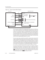
On-Chip Peripherals . . . . . . . . . . . . . . . . . . . . . . . . . . . . . . . . . . . . . . . . . . . . . . . . . . . . . . . . . . . . . 8-1
Describes the TMS320C54x DSP peripherals and how to control them. Includes information
about the general-purpose I/O pins, timers, clock, and host port interface.
8.1
8.2
8.3
8.4
8.5
8.6
9
Single-Access Memory and the Pipeline . . . . . . . . . . . . . . . . . . . . . . . . . . . . . . . . . . . . . .
Pipeline Latencies . . . . . . . . . . . . . . . . . . . . . . . . . . . . . . . . . . . . . . . . . . . . . . . . . . . . . . . . .
7.5.1 Recommended Instructions for Accessing Memory-Mapped Registers . . . . .
7.5.2 Updating ARx, BK, or SP—A Resolved Conflict . . . . . . . . . . . . . . . . . . . . . . . . .
7.5.3 Rules to Determine DAGEN Register Access Conflicts . . . . . . . . . . . . . . . . . .
7.5.4 Latencies for ARx and BK . . . . . . . . . . . . . . . . . . . . . . . . . . . . . . . . . . . . . . . . . . .
7.5.5 Latencies for the Stack Pointer . . . . . . . . . . . . . . . . . . . . . . . . . . . . . . . . . . . . . . .
7.5.6 Latencies for Temporary Register (T) . . . . . . . . . . . . . . . . . . . . . . . . . . . . . . . . . .
7.5.7 Latencies for Accessing Status Registers . . . . . . . . . . . . . . . . . . . . . . . . . . . . . .
7.5.8 Latencies in Repeat-Block Loops . . . . . . . . . . . . . . . . . . . . . . . . . . . . . . . . . . . . .
7.5.9 Latencies for the PMST . . . . . . . . . . . . . . . . . . . . . . . . . . . . . . . . . . . . . . . . . . . . .
7.5.10 Latencies for Memory-Mapped Accesses to Accumulators . . . . . . . . . . . . . . .
Available On-Chip Peripherals . . . . . . . . . . . . . . . . . . . . . . . . . . . . . . . . . . . . . . . . . . . . . . . . 8-2
Peripheral Memory-Mapped Registers . . . . . . . . . . . . . . . . . . . . . . . . . . . . . . . . . . . . . . . . . 8-2
General-Purpose I/O . . . . . . . . . . . . . . . . . . . . . . . . . . . . . . . . . . . . . . . . . . . . . . . . . . . . . . . 8-20
8.3.1 Branch Control Input Pin (BIO) . . . . . . . . . . . . . . . . . . . . . . . . . . . . . . . . . . . . . . . 8-20
8.3.2 External Flag Output Pin (XF) . . . . . . . . . . . . . . . . . . . . . . . . . . . . . . . . . . . . . . . . 8-20
Timer . . . . . . . . . . . . . . . . . . . . . . . . . . . . . . . . . . . . . . . . . . . . . . . . . . . . . . . . . . . . . . . . . . . . 8-21
8.4.1 Timer Registers . . . . . . . . . . . . . . . . . . . . . . . . . . . . . . . . . . . . . . . . . . . . . . . . . . . . 8-21
8.4.2 Timer Operation . . . . . . . . . . . . . . . . . . . . . . . . . . . . . . . . . . . . . . . . . . . . . . . . . . . . 8-23
Clock Generator . . . . . . . . . . . . . . . . . . . . . . . . . . . . . . . . . . . . . . . . . . . . . . . . . . . . . . . . . . . 8-26
8.5.1 Hardware-Configurable PLL . . . . . . . . . . . . . . . . . . . . . . . . . . . . . . . . . . . . . . . . . 8-26
8.5.2 Software-Programmable PLL . . . . . . . . . . . . . . . . . . . . . . . . . . . . . . . . . . . . . . . . 8-27
Host Port Interface . . . . . . . . . . . . . . . . . . . . . . . . . . . . . . . . . . . . . . . . . . . . . . . . . . . . . . . . . 8-36
8.6.1 Basic Host Port Interface Functional Description . . . . . . . . . . . . . . . . . . . . . . . . 8-37
8.6.2 Details of Host Port Interface Operation . . . . . . . . . . . . . . . . . . . . . . . . . . . . . . . 8-40
8.6.3 Host Read/Write Access to HPI . . . . . . . . . . . . . . . . . . . . . . . . . . . . . . . . . . . . . . 8-45
8.6.4 DSPINT and HINT Function Operation . . . . . . . . . . . . . . . . . . . . . . . . . . . . . . . . 8-50
8.6.5 Considerations in Changing HPI Memory Access Mode (SAM/HOM) and
IDLE2/3 Use . . . . . . . . . . . . . . . . . . . . . . . . . . . . . . . . . . . . . . . . . . . . . . . . . . . . . . . 8-51
8.6.6 Access of HPI Memory During Reset . . . . . . . . . . . . . . . . . . . . . . . . . . . . . . . . . . 8-53
Serial Ports . . . . . . . . . . . . . . . . . . . . . . . . . . . . . . . . . . . . . . . . . . . . . . . . . . . . . . . . . . . . . . . . . . . . . 9-1
Describes the TMS320C54x DSP serial ports. Includes information about the standard serial
port interface, buffered serial port interface, multichannel buffered serial port interface, and
time-division multiplexed serial port interface.
9.1
9.2
SPRU131G
Introduction to the Serial Ports . . . . . . . . . . . . . . . . . . . . . . . . . . . . . . . . . . . . . . . . . . . . . . .
Serial Port Interface . . . . . . . . . . . . . . . . . . . . . . . . . . . . . . . . . . . . . . . . . . . . . . . . . . . . . . . . .
9.2.1 Serial Port Interface Registers . . . . . . . . . . . . . . . . . . . . . . . . . . . . . . . . . . . . . . . . .
9.2.2 Serial Port Interface Operation . . . . . . . . . . . . . . . . . . . . . . . . . . . . . . . . . . . . . . . .
Contents
9-2
9-4
9-5
9-6
xix
Contents
9.3
9.4
9.2.3 Configuring the Serial Port Interface . . . . . . . . . . . . . . . . . . . . . . . . . . . . . . . . . . . 9-8
9.2.4 Burst Mode Transmit and Receive Operations . . . . . . . . . . . . . . . . . . . . . . . . . . 9-18
9.2.5 Continuous Mode Transmit and Receive Operations . . . . . . . . . . . . . . . . . . . . 9-24
9.2.6 Serial Port Interface Exception Conditions . . . . . . . . . . . . . . . . . . . . . . . . . . . . . 9-26
9.2.7 Example of Serial Port Interface Operation . . . . . . . . . . . . . . . . . . . . . . . . . . . . . 9-31
Buffered Serial Port (BSP) Interface . . . . . . . . . . . . . . . . . . . . . . . . . . . . . . . . . . . . . . . . . . 9-33
9.3.1 BSP Operation in Standard Mode . . . . . . . . . . . . . . . . . . . . . . . . . . . . . . . . . . . . . 9-35
9.3.2 Autobuffering Unit (ABU) Operation . . . . . . . . . . . . . . . . . . . . . . . . . . . . . . . . . . . 9-40
9.3.3 System Considerations for BSP Operation . . . . . . . . . . . . . . . . . . . . . . . . . . . . . 9-49
9.3.4 Buffer Misalignment Interrupt (BMINT) – C549 only . . . . . . . . . . . . . . . . . . . . . 9-54
9.3.5 BSP Operation in Power-Down Mode . . . . . . . . . . . . . . . . . . . . . . . . . . . . . . . . . 9-55
Time-Division Multiplexed (TDM) Serial Port Interface . . . . . . . . . . . . . . . . . . . . . . . . . . 9-56
9.4.1 Basic Time-Division Multiplexed Operation . . . . . . . . . . . . . . . . . . . . . . . . . . . . . 9-56
9.4.2 TDM Serial Port Interface Registers . . . . . . . . . . . . . . . . . . . . . . . . . . . . . . . . . . . 9-56
9.4.3 TDM Serial Port Interface Operation . . . . . . . . . . . . . . . . . . . . . . . . . . . . . . . . . . 9-58
9.4.4 TDM Mode Transmit and Receive Operations . . . . . . . . . . . . . . . . . . . . . . . . . . 9-62
9.4.5 TDM Serial Port Interface Exception Conditions . . . . . . . . . . . . . . . . . . . . . . . . 9-64
9.4.6 Examples of TDM Serial Port Interface Operation . . . . . . . . . . . . . . . . . . . . . . . 9-64
10 External Bus Operation . . . . . . . . . . . . . . . . . . . . . . . . . . . . . . . . . . . . . . . . . . . . . . . . . . . . . . . . . 10-1
Discusses the external bus interface and the timing of events involved in memory and I/O
accesses. Describes the hold mode and the wake-up sequence from IDLE3 mode.
10.1
10.2
10.3
10.4
10.5
10.6
A
Design Considerations for Using XDS510 Emulator . . . . . . . . . . . . . . . . . . . . . . . . . . . . . . . . A-1
Describes the JTAG emulator cable, how to construct a 14-pin connector on your target system,
and how to connect the target system to the emulator.
A.1
A.2
A.3
xx
External Bus Interface . . . . . . . . . . . . . . . . . . . . . . . . . . . . . . . . . . . . . . . . . . . . . . . . . . . . . . 10-2
External Bus Priority . . . . . . . . . . . . . . . . . . . . . . . . . . . . . . . . . . . . . . . . . . . . . . . . . . . . . . . 10-4
External Bus Control . . . . . . . . . . . . . . . . . . . . . . . . . . . . . . . . . . . . . . . . . . . . . . . . . . . . . . . 10-5
10.3.1 Wait-State Generator . . . . . . . . . . . . . . . . . . . . . . . . . . . . . . . . . . . . . . . . . . . . . . . 10-5
10.3.2 Bank-Switching Logic . . . . . . . . . . . . . . . . . . . . . . . . . . . . . . . . . . . . . . . . . . . . . . . 10-9
External Bus Interface Timing . . . . . . . . . . . . . . . . . . . . . . . . . . . . . . . . . . . . . . . . . . . . . . 10-14
10.4.1 Memory Access Timing . . . . . . . . . . . . . . . . . . . . . . . . . . . . . . . . . . . . . . . . . . . . 10-14
10.4.2 I/O Access Timing . . . . . . . . . . . . . . . . . . . . . . . . . . . . . . . . . . . . . . . . . . . . . . . . . 10-18
10.4.3 Memory and I/O Access Timing . . . . . . . . . . . . . . . . . . . . . . . . . . . . . . . . . . . . . 10-19
Start-Up Access Sequences . . . . . . . . . . . . . . . . . . . . . . . . . . . . . . . . . . . . . . . . . . . . . . . 10-24
10.5.1 Reset . . . . . . . . . . . . . . . . . . . . . . . . . . . . . . . . . . . . . . . . . . . . . . . . . . . . . . . . . . . . 10-24
10.5.2 IDLE3 . . . . . . . . . . . . . . . . . . . . . . . . . . . . . . . . . . . . . . . . . . . . . . . . . . . . . . . . . . . . 10-26
Hold Mode . . . . . . . . . . . . . . . . . . . . . . . . . . . . . . . . . . . . . . . . . . . . . . . . . . . . . . . . . . . . . . . 10-28
10.6.1 Interrupts During Hold . . . . . . . . . . . . . . . . . . . . . . . . . . . . . . . . . . . . . . . . . . . . . . 10-29
10.6.2 Hold and Reset . . . . . . . . . . . . . . . . . . . . . . . . . . . . . . . . . . . . . . . . . . . . . . . . . . . 10-29
Designing Your Target System’s Emulator Connector (14-Pin Header) . . . . . . . . . . . . . A-2
Bus Protocol . . . . . . . . . . . . . . . . . . . . . . . . . . . . . . . . . . . . . . . . . . . . . . . . . . . . . . . . . . . . . . . A-4
Emulator Cable Pod . . . . . . . . . . . . . . . . . . . . . . . . . . . . . . . . . . . . . . . . . . . . . . . . . . . . . . . . A-5
Contents
SPRU131G
Contents
A.4
A.5
A.6
A.7
A.8
B
Emulator Cable Pod Signal Timing . . . . . . . . . . . . . . . . . . . . . . . . . . . . . . . . . . . . . . . . . . . . A-6
Emulation Timing Calculations . . . . . . . . . . . . . . . . . . . . . . . . . . . . . . . . . . . . . . . . . . . . . . . . A-7
Connections Between the Emulator and the Target System . . . . . . . . . . . . . . . . . . . . . A-10
A.6.1 Buffering Signals . . . . . . . . . . . . . . . . . . . . . . . . . . . . . . . . . . . . . . . . . . . . . . . . . . . A-10
A.6.2 Using a Target-System Clock . . . . . . . . . . . . . . . . . . . . . . . . . . . . . . . . . . . . . . . . A-12
A.6.3 Configuring Multiple Processors . . . . . . . . . . . . . . . . . . . . . . . . . . . . . . . . . . . . . . A-13
Physical Dimensions for the 14-Pin Emulator Connector . . . . . . . . . . . . . . . . . . . . . . . . A-14
Emulation Design Considerations . . . . . . . . . . . . . . . . . . . . . . . . . . . . . . . . . . . . . . . . . . . . A-16
A.8.1 Using Scan Path Linkers . . . . . . . . . . . . . . . . . . . . . . . . . . . . . . . . . . . . . . . . . . . . A-16
A.8.2 Emulation Timing Calculations for a Scan Path Linker (SPL) . . . . . . . . . . . . . A-18
A.8.3 Using Emulation Pins . . . . . . . . . . . . . . . . . . . . . . . . . . . . . . . . . . . . . . . . . . . . . . . A-20
A.8.4 Performing Diagnostic Applications . . . . . . . . . . . . . . . . . . . . . . . . . . . . . . . . . . . A-24
Development Support and Part Order Information . . . . . . . . . . . . . . . . . . . . . . . . . . . . . . . . . B-1
Provides device part numbers and support tool ordering information for the TMS320C54x DSP
and development support information available from TI and third-party vendors.
B.1
B.2
Development Support . . . . . . . . . . . . . . . . . . . . . . . . . . . . . . . . . . . . . . . . . . . . . . . . . . . . . . .
B.1.1 Development Tools . . . . . . . . . . . . . . . . . . . . . . . . . . . . . . . . . . . . . . . . . . . . . . . . . .
B.1.2 Third-Party Support . . . . . . . . . . . . . . . . . . . . . . . . . . . . . . . . . . . . . . . . . . . . . . . . . .
B.1.3 Technical Training Organization (TTO) TMS320 DSP Workshops . . . . . . . . . .
B.1.4 Assistance . . . . . . . . . . . . . . . . . . . . . . . . . . . . . . . . . . . . . . . . . . . . . . . . . . . . . . . . . .
Part Order Information . . . . . . . . . . . . . . . . . . . . . . . . . . . . . . . . . . . . . . . . . . . . . . . . . . . . . .
B.2.1 Device and Development Support Tool Nomenclature Prefixes . . . . . . . . . . . .
B.2.2 Device Nomenclature . . . . . . . . . . . . . . . . . . . . . . . . . . . . . . . . . . . . . . . . . . . . . . . .
B.2.3 Development Support Tools . . . . . . . . . . . . . . . . . . . . . . . . . . . . . . . . . . . . . . . . . . .
B-2
B-2
B-3
B-4
B-4
B-5
B-5
B-6
B-7
C
Submitting ROM Codes to TI . . . . . . . . . . . . . . . . . . . . . . . . . . . . . . . . . . . . . . . . . . . . . . . . . . . . . C-1
Provides information for submitting ROM codes to Texas Instruments.
D
Glossary . . . . . . . . . . . . . . . . . . . . . . . . . . . . . . . . . . . . . . . . . . . . . . . . . . . . . . . . . . . . . . . . . . . . . . . . D-1
Defines terms and abbreviations used throughout this book.
SPRU131G
Contents
xxi
Figures
Figures
1–1
2–1
3–1
3–2
3–3
3–4
3–5
3–6
3–7
3–8
3–9
3–10
3–11
3–12
3–13
3–14
3–15
3–16
3–17
3–18
3–19
4–1
4–2
4–3
4–4
4–5
4–6
4–7
4–8
4–9
4–10
4–11
xxii
Evolution of the TMS320 DSP Family . . . . . . . . . . . . . . . . . . . . . . . . . . . . . . . . . . . . . . . . . . 1-3
Block Diagram of TMS320C54x DSP Internal Hardware . . . . . . . . . . . . . . . . . . . . . . . . . . . . 2-2
Memory Maps for the C541 . . . . . . . . . . . . . . . . . . . . . . . . . . . . . . . . . . . . . . . . . . . . . . . . . . . . . 3-3
Memory Maps for the C542 and C543 . . . . . . . . . . . . . . . . . . . . . . . . . . . . . . . . . . . . . . . . . . . 3-4
Memory Maps for the C545 and C546 . . . . . . . . . . . . . . . . . . . . . . . . . . . . . . . . . . . . . . . . . . . 3-5
Memory Maps for the C548 . . . . . . . . . . . . . . . . . . . . . . . . . . . . . . . . . . . . . . . . . . . . . . . . . . . . . 3-6
Memory Maps for the C549 . . . . . . . . . . . . . . . . . . . . . . . . . . . . . . . . . . . . . . . . . . . . . . . . . . . . . 3-7
Extended Program Memory Maps for the C548 and C549 . . . . . . . . . . . . . . . . . . . . . . . . . . 3-8
Memory Maps for the C5402 . . . . . . . . . . . . . . . . . . . . . . . . . . . . . . . . . . . . . . . . . . . . . . . . . . . 3-9
Extended Program Memory for the C5402 . . . . . . . . . . . . . . . . . . . . . . . . . . . . . . . . . . . . . . . 3-10
Memory Maps for the C5410 . . . . . . . . . . . . . . . . . . . . . . . . . . . . . . . . . . . . . . . . . . . . . . . . . . 3-11
Extended Program Memory Maps for the C5410
(On-chip RAM Not Mapped in Program Space and Data Space, OVLY = 0) . . . . . . . . . . 3-12
Extended Program Memory Maps for the C5410
(On-chip RAM Mapped in Program Space and Data Space, OVLY = 1) . . . . . . . . . . . . . 3-12
Data Memory Map for the C5420 Relative to CPU Subsystems A and B . . . . . . . . . . . . . 3-13
Program Memory Maps for the C5420 Relative to CPU Subsystems A and B . . . . . . . . 3-14
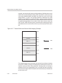
On-Chip ROM Block Organization . . . . . . . . . . . . . . . . . . . . . . . . . . . . . . . . . . . . . . . . . . . . . . 3-17
On-Chip ROM Program Memory Map (High Addresses) . . . . . . . . . . . . . . . . . . . . . . . . . . . 3-19
Extended Program Memory With On-Chip RAM Not Mapped
in Program Space (OVLY = 0) . . . . . . . . . . . . . . . . . . . . . . . . . . . . . . . . . . . . . . . . . . . . . . . . . 3-20
Extended Program Memory With On-Chip RAM Mapped in Program Space
and Data Space (OVLY = 1) . . . . . . . . . . . . . . . . . . . . . . . . . . . . . . . . . . . . . . . . . . . . . . . . . . . 3-21
On-Chip RAM Block Organization . . . . . . . . . . . . . . . . . . . . . . . . . . . . . . . . . . . . . . . . . . . . . . 3-24
On-Chip RAM Block Organization (C5402/C5410/C5420) . . . . . . . . . . . . . . . . . . . . . . . . . 3-25
Status Register 0 (ST0) Diagram . . . . . . . . . . . . . . . . . . . . . . . . . . . . . . . . . . . . . . . . . . . . . . . . 4-2
Status Register 1 (ST1) Diagram . . . . . . . . . . . . . . . . . . . . . . . . . . . . . . . . . . . . . . . . . . . . . . . . 4-4
Processor Mode Status Register (PMST) Diagram . . . . . . . . . . . . . . . . . . . . . . . . . . . . . . . . 4-6
ALU Functional Diagram . . . . . . . . . . . . . . . . . . . . . . . . . . . . . . . . . . . . . . . . . . . . . . . . . . . . . . 4-10
Accumulator A . . . . . . . . . . . . . . . . . . . . . . . . . . . . . . . . . . . . . . . . . . . . . . . . . . . . . . . . . . . . . . . 4-13
Accumulator B . . . . . . . . . . . . . . . . . . . . . . . . . . . . . . . . . . . . . . . . . . . . . . . . . . . . . . . . . . . . . . . 4-13
Barrel Shifter Functional Diagram . . . . . . . . . . . . . . . . . . . . . . . . . . . . . . . . . . . . . . . . . . . . . . 4-18
Multiplier/Adder Functional Diagram . . . . . . . . . . . . . . . . . . . . . . . . . . . . . . . . . . . . . . . . . . . . 4-20
Compare, Select, and Store Unit (CSSU) . . . . . . . . . . . . . . . . . . . . . . . . . . . . . . . . . . . . . . . . 4-24
Viterbi Operator . . . . . . . . . . . . . . . . . . . . . . . . . . . . . . . . . . . . . . . . . . . . . . . . . . . . . . . . . . . . . . 4-25
Exponent Encoder . . . . . . . . . . . . . . . . . . . . . . . . . . . . . . . . . . . . . . . . . . . . . . . . . . . . . . . . . . . 4-27
Figures
SPRU131G
Figures
5–1
5–2
5–3
5–4
5–5
5–6
5–7
5–8
5–9
5–10
5–11
5–12
5–13
5–14
5–15
5–16
5–17
6–1
6–2
6–3
6–4
6–5
7–1
7–2
7–3
8–1
8–2
8–3
8–4
8–5
8–6
8–7
8–8
8–9
8–10
8–11
8–12
8–13
9–1
9–2
9–3
9–4
9–5
9–6
RPT Instruction With Short-Immediate Addressing . . . . . . . . . . . . . . . . . . . . . . . . . . . . . . . . . 5-3
RPT Instruction With 16-Bit-Immediate Addressing . . . . . . . . . . . . . . . . . . . . . . . . . . . . . . . . 5-3
Direct-Addressing Instruction Format . . . . . . . . . . . . . . . . . . . . . . . . . . . . . . . . . . . . . . . . . . . . 5-8
Direct Addressing Block Diagram . . . . . . . . . . . . . . . . . . . . . . . . . . . . . . . . . . . . . . . . . . . . . . . 5-8
DP-Referenced Direct Address . . . . . . . . . . . . . . . . . . . . . . . . . . . . . . . . . . . . . . . . . . . . . . . . . 5-9
SP-Referenced Direct Address . . . . . . . . . . . . . . . . . . . . . . . . . . . . . . . . . . . . . . . . . . . . . . . . . 5-9
Indirect-Addressing Instruction Format for a Single Data-Memory Operand . . . . . . . . . . 5-10
Indirect Addressing Block Diagram for a Single Data-Memory Operand . . . . . . . . . . . . . 5-12
Circular Addressing Block Diagram . . . . . . . . . . . . . . . . . . . . . . . . . . . . . . . . . . . . . . . . . . . . . 5-17
Circular Buffer Implementation . . . . . . . . . . . . . . . . . . . . . . . . . . . . . . . . . . . . . . . . . . . . . . . . . 5-17
Indirect-Addressing Instruction Format for Dual Data-Memory Operands . . . . . . . . . . . . 5-20
Indirect Addressing Block Diagram for Dual Data-Memory Operands . . . . . . . . . . . . . . . 5-21
How ARP Indexes the Auxiliary Registers . . . . . . . . . . . . . . . . . . . . . . . . . . . . . . . . . . . . . . . 5-23
Indirect-Addressing Instruction Format for Compatibility Mode . . . . . . . . . . . . . . . . . . . . . 5-24
Memory-Mapped Register Addressing Block Diagram . . . . . . . . . . . . . . . . . . . . . . . . . . . . 5-25
Stack and Stack Pointer Before and After a Push Operation . . . . . . . . . . . . . . . . . . . . . . . 5-27
Word Order in Memory . . . . . . . . . . . . . . . . . . . . . . . . . . . . . . . . . . . . . . . . . . . . . . . . . . . . . . . 5-29
Program-Address Generation Logic (PAGEN) Registers . . . . . . . . . . . . . . . . . . . . . . . . . . . . 6-3
Interrupt Flag Register (IFR) Diagram . . . . . . . . . . . . . . . . . . . . . . . . . . . . . . . . . . . . . . . . . . . 6-28
Interrupt Mask Register (IMR) Diagram . . . . . . . . . . . . . . . . . . . . . . . . . . . . . . . . . . . . . . . . . 6-29
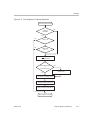
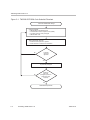
Interrupt-Vector Address Generation . . . . . . . . . . . . . . . . . . . . . . . . . . . . . . . . . . . . . . . . . . . . 6-36
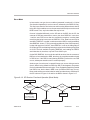
Flow Diagram of Interrupt Operation . . . . . . . . . . . . . . . . . . . . . . . . . . . . . . . . . . . . . . . . . . . . 6-37
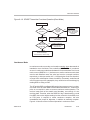
Pipeline Stages . . . . . . . . . . . . . . . . . . . . . . . . . . . . . . . . . . . . . . . . . . . . . . . . . . . . . . . . . . . . . . . 7-3
Pipelined Memory Accesses . . . . . . . . . . . . . . . . . . . . . . . . . . . . . . . . . . . . . . . . . . . . . . . . . . . . 7-4
Half-Cycle Accesses to Dual-Access Memory . . . . . . . . . . . . . . . . . . . . . . . . . . . . . . . . . . . . 7-28
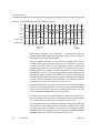
External Flag Timing Diagram . . . . . . . . . . . . . . . . . . . . . . . . . . . . . . . . . . . . . . . . . . . . . . . . . 8-20
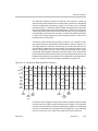
Timer Control Register (TCR) Diagram . . . . . . . . . . . . . . . . . . . . . . . . . . . . . . . . . . . . . . . . . . 8-22
Timer Block Diagram . . . . . . . . . . . . . . . . . . . . . . . . . . . . . . . . . . . . . . . . . . . . . . . . . . . . . . . . . 8-23
Clock Mode Register (CLKMD) Diagram . . . . . . . . . . . . . . . . . . . . . . . . . . . . . . . . . . . . . . . . 8-29
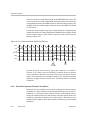
PLL Lockup Time Versus CLKOUT Frequency . . . . . . . . . . . . . . . . . . . . . . . . . . . . . . . . . . . 8-31
Host Port Interface Block Diagram . . . . . . . . . . . . . . . . . . . . . . . . . . . . . . . . . . . . . . . . . . . . . . 8-36
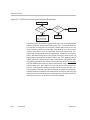
Generic System Block Diagram . . . . . . . . . . . . . . . . . . . . . . . . . . . . . . . . . . . . . . . . . . . . . . . . 8-38
Select Input Logic . . . . . . . . . . . . . . . . . . . . . . . . . . . . . . . . . . . . . . . . . . . . . . . . . . . . . . . . . . . . 8-42
HPIC Diagram — Host Reads from HPIC . . . . . . . . . . . . . . . . . . . . . . . . . . . . . . . . . . . . . . . 8-44
HPIC Diagram — Host Writes to HPIC . . . . . . . . . . . . . . . . . . . . . . . . . . . . . . . . . . . . . . . . . . 8-45
HPIC Diagram — TMS320C54x DSP Reads From HPIC . . . . . . . . . . . . . . . . . . . . . . . . . . 8-45
HPIC Diagram — TMS320C54x DSP Writes to HPIC . . . . . . . . . . . . . . . . . . . . . . . . . . . . . 8-45
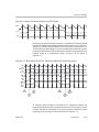
HPI Timing Diagram . . . . . . . . . . . . . . . . . . . . . . . . . . . . . . . . . . . . . . . . . . . . . . . . . . . . . . . . . . 8-47
One-Way Serial Port Transfer . . . . . . . . . . . . . . . . . . . . . . . . . . . . . . . . . . . . . . . . . . . . . . . . . . . 9-7
Serial Port Interface Block Diagram . . . . . . . . . . . . . . . . . . . . . . . . . . . . . . . . . . . . . . . . . . . . . . 9-8
Serial Port Control Register (SPC) Diagram . . . . . . . . . . . . . . . . . . . . . . . . . . . . . . . . . . . . . . 9-8
Receiver Signal Multiplexers . . . . . . . . . . . . . . . . . . . . . . . . . . . . . . . . . . . . . . . . . . . . . . . . . . . 9-13
Burst Mode Serial Port Transmit Operation . . . . . . . . . . . . . . . . . . . . . . . . . . . . . . . . . . . . . . 9-18
Serial Port Transmit With Long FSX Pulse . . . . . . . . . . . . . . . . . . . . . . . . . . . . . . . . . . . . . . . 9-19
SPRU131G
Figures
xxiii
Figures
9–7
9–8
9–9
9–10
9–11
9–12
9–13
9–14
9–15
9–16
9–17
9–18
9–19
9–20
9–21
9–22
9–23
9–24
9–25
9–26
9–27
9–28
9–29
9–30
9–31
9–32
9–33
9–34
10–1
10–2
10–3
10–4
10–5
10–6
10–7
10–8
10–9
10–10
10–11
10–12
10–13
10–14
xxiv
Burst Mode Serial Port Transmit Operation With Delayed Frame Sync
in External Frame Sync Mode (SP) . . . . . . . . . . . . . . . . . . . . . . . . . . . . . . . . . . . . . . . . . . . . . 9-20
Burst Mode Serial Port Transmit Operation With Delayed Frame Sync
in External Frame Sync Mode (BSP) . . . . . . . . . . . . . . . . . . . . . . . . . . . . . . . . . . . . . . . . . . . . 9-21
Burst Mode Serial Port Receive Operation . . . . . . . . . . . . . . . . . . . . . . . . . . . . . . . . . . . . . . . 9-21
Burst Mode Serial Port Receive Overrun . . . . . . . . . . . . . . . . . . . . . . . . . . . . . . . . . . . . . . . . 9-22
Serial Port Receive With Long FSR Pulse . . . . . . . . . . . . . . . . . . . . . . . . . . . . . . . . . . . . . . . 9-23
Burst Mode Serial Port Transmit at Maximum Packet Frequency . . . . . . . . . . . . . . . . . . . 9-23
Burst Mode Serial Port Receive at Maximum Packet Frequency . . . . . . . . . . . . . . . . . . . . 9-24
Continuous Mode Serial Port Transmit . . . . . . . . . . . . . . . . . . . . . . . . . . . . . . . . . . . . . . . . . . 9-25
Continuous Mode Serial Port Receive . . . . . . . . . . . . . . . . . . . . . . . . . . . . . . . . . . . . . . . . . . 9-26
SP Receiver Functional Operation (Burst Mode) . . . . . . . . . . . . . . . . . . . . . . . . . . . . . . . . . 9-27
BSP Receiver Functional Operation (Burst Mode) . . . . . . . . . . . . . . . . . . . . . . . . . . . . . . . . 9-28
SP/BSP Transmitter Functional Operation (Burst Mode) . . . . . . . . . . . . . . . . . . . . . . . . . . . 9-29
SP/BSP Receiver Functional Operation (Continuous Mode) . . . . . . . . . . . . . . . . . . . . . . . 9-30
SP/BSP Transmitter Functional Operation (Continuous Mode) . . . . . . . . . . . . . . . . . . . . . 9-31
BSP Block Diagram . . . . . . . . . . . . . . . . . . . . . . . . . . . . . . . . . . . . . . . . . . . . . . . . . . . . . . . . . . 9-34
BSP Control Extension Register (BSPCE) Diagram — Serial Port Control Bits . . . . . . . 9-37
Transmit Continuous Mode with External Frame and FIG = 1 (Format Is 16 Bits) . . . . . 9-40
ABU Block Diagram . . . . . . . . . . . . . . . . . . . . . . . . . . . . . . . . . . . . . . . . . . . . . . . . . . . . . . . . . . 9-42
BSP Control Extension Register (BSPCE) Diagram — ABU Control Bits . . . . . . . . . . . . . 9-43
Circular Addressing Registers . . . . . . . . . . . . . . . . . . . . . . . . . . . . . . . . . . . . . . . . . . . . . . . . . 9-47
Transmit Buffer and Receive Buffer Mapping Example . . . . . . . . . . . . . . . . . . . . . . . . . . . . 9-48
Standard Mode BSP Initialization Timing . . . . . . . . . . . . . . . . . . . . . . . . . . . . . . . . . . . . . . . . 9-51
Autobuffering Mode Initialization Timing . . . . . . . . . . . . . . . . . . . . . . . . . . . . . . . . . . . . . . . . . 9-52
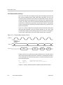
Time-Division Multiplexing . . . . . . . . . . . . . . . . . . . . . . . . . . . . . . . . . . . . . . . . . . . . . . . . . . . . . 9-56
TDM 4-Wire Bus . . . . . . . . . . . . . . . . . . . . . . . . . . . . . . . . . . . . . . . . . . . . . . . . . . . . . . . . . . . . . 9-58
TDM Serial Port Registers Diagram . . . . . . . . . . . . . . . . . . . . . . . . . . . . . . . . . . . . . . . . . . . . 9-60
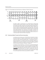
Serial Port Timing (TDM Mode) . . . . . . . . . . . . . . . . . . . . . . . . . . . . . . . . . . . . . . . . . . . . . . . . 9-62
TDM Example Configuration Diagram . . . . . . . . . . . . . . . . . . . . . . . . . . . . . . . . . . . . . . . . . . . 9-65
External Bus Interface Priority . . . . . . . . . . . . . . . . . . . . . . . . . . . . . . . . . . . . . . . . . . . . . . . . . 10-4
Software Wait-State Register (SWWSR) Diagram . . . . . . . . . . . . . . . . . . . . . . . . . . . . . . . . 10-5
Software Wait-State Control Register (SWCR) Diagram . . . . . . . . . . . . . . . . . . . . . . . . . . . 10-6
Software Wait-State Generator Block Diagram . . . . . . . . . . . . . . . . . . . . . . . . . . . . . . . . . . . 10-8
Bank-Switching Control Register (BSCR) Diagram . . . . . . . . . . . . . . . . . . . . . . . . . . . . . . . 10-9
Bank Switching Between Memory Reads . . . . . . . . . . . . . . . . . . . . . . . . . . . . . . . . . . . . . . . 10-12
Bank Switching Between Program Space and Data Space . . . . . . . . . . . . . . . . . . . . . . . 10-13
Memory Interface Operation for Read-Read-Write . . . . . . . . . . . . . . . . . . . . . . . . . . . . . . . 10-15
Memory Interface Operation for Write-Write-Read . . . . . . . . . . . . . . . . . . . . . . . . . . . . . . . 10-16
Memory Interface Operation for Read-Read-Write (Program-Space Wait States) . . . . 10-17
Parallel I/O Interface Operation for Read–Write–Read . . . . . . . . . . . . . . . . . . . . . . . . . . . 10-18
Parallel I/O Operation for Read-Write-Read (I/O-Space Wait States) . . . . . . . . . . . . . . . 10-19
Memory Read and I/O Write . . . . . . . . . . . . . . . . . . . . . . . . . . . . . . . . . . . . . . . . . . . . . . . . . . 10-20
Memory Read and I/O Read . . . . . . . . . . . . . . . . . . . . . . . . . . . . . . . . . . . . . . . . . . . . . . . . . . 10-20
Figures
SPRU131G
Figures
10–15
10–16
10–17
10–18
10–19
10–20
10–21
10–22
10–23
10–24
A–1
A–2
A–3
A–4
A–5
A–6
A–7
A–8
A–9
A–10
A–11
A–12
A–13
A–14
A–15
B–1
C–1
Memory Write and I/O Write . . . . . . . . . . . . . . . . . . . . . . . . . . . . . . . . . . . . . . . . . . . . . . . . . . 10-21
Memory Write and I/O Read . . . . . . . . . . . . . . . . . . . . . . . . . . . . . . . . . . . . . . . . . . . . . . . . . . 10-21
I/O Write and Memory Write . . . . . . . . . . . . . . . . . . . . . . . . . . . . . . . . . . . . . . . . . . . . . . . . . . 10-22
I/O Write and Memory Read . . . . . . . . . . . . . . . . . . . . . . . . . . . . . . . . . . . . . . . . . . . . . . . . . . 10-22
I/O Read and Memory Write . . . . . . . . . . . . . . . . . . . . . . . . . . . . . . . . . . . . . . . . . . . . . . . . . . 10-23
I/O Read and Memory Read . . . . . . . . . . . . . . . . . . . . . . . . . . . . . . . . . . . . . . . . . . . . . . . . . . 10-23
External Bus Reset Sequence . . . . . . . . . . . . . . . . . . . . . . . . . . . . . . . . . . . . . . . . . . . . . . . . 10-25
IDLE3 Wake-Up Sequence . . . . . . . . . . . . . . . . . . . . . . . . . . . . . . . . . . . . . . . . . . . . . . . . . . . 10-27
HOLD and HOLDA Minimum Timing for HM = 0 . . . . . . . . . . . . . . . . . . . . . . . . . . . . . . . . . 10-30
HOLD and RS Interaction . . . . . . . . . . . . . . . . . . . . . . . . . . . . . . . . . . . . . . . . . . . . . . . . . . . . 10-31
14-Pin Header Signals and Header Dimensions . . . . . . . . . . . . . . . . . . . . . . . . . . . . . . . . . . . A-2
Emulator Cable Pod Interface . . . . . . . . . . . . . . . . . . . . . . . . . . . . . . . . . . . . . . . . . . . . . . . . . . . A-5
Emulator Cable Pod Timings . . . . . . . . . . . . . . . . . . . . . . . . . . . . . . . . . . . . . . . . . . . . . . . . . . . A-6
Emulator Connections Without Signal Buffering . . . . . . . . . . . . . . . . . . . . . . . . . . . . . . . . . . A-10
Emulator Connections With Signal Buffering . . . . . . . . . . . . . . . . . . . . . . . . . . . . . . . . . . . . . A-11
Target-System-Generated Test Clock . . . . . . . . . . . . . . . . . . . . . . . . . . . . . . . . . . . . . . . . . . . A-12
Multiprocessor Connections . . . . . . . . . . . . . . . . . . . . . . . . . . . . . . . . . . . . . . . . . . . . . . . . . . . A-13
Pod/Connector Dimensions . . . . . . . . . . . . . . . . . . . . . . . . . . . . . . . . . . . . . . . . . . . . . . . . . . . A-14
14-Pin Connector Dimensions . . . . . . . . . . . . . . . . . . . . . . . . . . . . . . . . . . . . . . . . . . . . . . . . . A-15
Connecting a Secondary JTAG Scan Path to a Scan Path Linker . . . . . . . . . . . . . . . . . . . A-17
EMU0/1 Configuration to Meet Timing Requirements of Less Than 25 ns . . . . . . . . . . . . A-21
Suggested Timings for the EMU0 and EMU1 Signals . . . . . . . . . . . . . . . . . . . . . . . . . . . . . A-22
EMU0/1 Configuration With Additional AND Gate to Meet
Timing Requirements of Greater Than 25 ns . . . . . . . . . . . . . . . . . . . . . . . . . . . . . . . . . . . . . A-23
EMU0/1 Configuration Without Global Stop . . . . . . . . . . . . . . . . . . . . . . . . . . . . . . . . . . . . . . A-24
TBC Emulation Connections for n JTAG Scan Paths . . . . . . . . . . . . . . . . . . . . . . . . . . . . . . A-25
TMS320 DSP Device Nomenclature . . . . . . . . . . . . . . . . . . . . . . . . . . . . . . . . . . . . . . . . . . . . . B-6
TMS320 DSP ROM Code Submittal Flowchart . . . . . . . . . . . . . . . . . . . . . . . . . . . . . . . . . . . . C-2
SPRU131G
Figures
xxv
Tables
Tables
1–1
2–1
2–2
2–3
2–4
3–1
3–2
3–3
3–4
3–5
4–1
4–2
4–3
4–4
4–5
4–6
5–1
5–2
5–3
5–4
5–5
5–6
5–7
5–8
5–9
5–10
5–11
6–1
6–2
6–3
6–4
6–5
6–6
6–7
6–8
6–9
xxvi
Typical Applications for the TMS320 DSPs . . . . . . . . . . . . . . . . . . . . . . . . . . . . . . . . . . . . . . . 1-4
Bus Usage for Read and Write Accesses . . . . . . . . . . . . . . . . . . . . . . . . . . . . . . . . . . . . . . . . . 2-4
Program and Data Memory on the TMS320C54x Devices . . . . . . . . . . . . . . . . . . . . . . . . . . 2-5
Host Port Interfaces on the TMS320C54x Devices . . . . . . . . . . . . . . . . . . . . . . . . . . . . . . . . 2-14
Serial Port Interfaces on the TMS320C54x Devices . . . . . . . . . . . . . . . . . . . . . . . . . . . . . . . 2-15
On-Chip Program Memory Available on TMS320C54x Devices . . . . . . . . . . . . . . . . . . . . 3-15
On-Chip Data Memory Available on the TMS320C54x Devices . . . . . . . . . . . . . . . . . . . . . 3-22
CPU Memory-Mapped Registers . . . . . . . . . . . . . . . . . . . . . . . . . . . . . . . . . . . . . . . . . . . . . . . 3-27
Memory Security Modes . . . . . . . . . . . . . . . . . . . . . . . . . . . . . . . . . . . . . . . . . . . . . . . . . . . . . . 3-30
HPI Access in Memory Security Modes for Specific Devices . . . . . . . . . . . . . . . . . . . . . . . 3-30
Status Register 0 (ST0) Bit Summary . . . . . . . . . . . . . . . . . . . . . . . . . . . . . . . . . . . . . . . . . . . 4-2
Status Register 1 (ST1) Bit Summary . . . . . . . . . . . . . . . . . . . . . . . . . . . . . . . . . . . . . . . . . . . 4-4
Processor Mode Status Register (PMST) Bit Summary . . . . . . . . . . . . . . . . . . . . . . . . . . . . 4-6
ALU Input Selection for ADD Instructions . . . . . . . . . . . . . . . . . . . . . . . . . . . . . . . . . . . . . . . . 4-11
Multiplier Input Selection for Several Instructions . . . . . . . . . . . . . . . . . . . . . . . . . . . . . . . . . 4-21
ALU Operations in Dual 16-Bit Mode . . . . . . . . . . . . . . . . . . . . . . . . . . . . . . . . . . . . . . . . . . . 4-25
Instructions That Allow Immediate Addressing . . . . . . . . . . . . . . . . . . . . . . . . . . . . . . . . . . . . 5-2
Direct-Addressing Instruction Bit Summary . . . . . . . . . . . . . . . . . . . . . . . . . . . . . . . . . . . . . . . 5-8
Indirect-Addressing Instruction Bit Summary – Single Data-Memory Operand . . . . . . . 5-10
Indirect Addressing Types With a Single Data-Memory Operand . . . . . . . . . . . . . . . . . . . 5-13
Bit-Reversed Addresses . . . . . . . . . . . . . . . . . . . . . . . . . . . . . . . . . . . . . . . . . . . . . . . . . . . . . . 5-19
Indirect-Addressing Instruction Bit Summary – Dual Data-Memory Operands . . . . . . . . 5-20
Auxiliary Registers Selected by Xar and Yar Field of Instruction . . . . . . . . . . . . . . . . . . . . 5-20
Indirect Addressing Types With Dual Data-Memory Operands . . . . . . . . . . . . . . . . . . . . . 5-21
Assembler Syntax Comparison to TMS320C54x DSP . . . . . . . . . . . . . . . . . . . . . . . . . . . . . 5-23
Indirect-Addressing Instruction Bit Summary – Compatibility Mode . . . . . . . . . . . . . . . . . 5-24
Instructions With 32-Bit Word Operands . . . . . . . . . . . . . . . . . . . . . . . . . . . . . . . . . . . . . . . . . 5-28
Devices With Additional Program Memory Address Lines . . . . . . . . . . . . . . . . . . . . . . . . . . . 6-2
Loading Addresses Into PC . . . . . . . . . . . . . . . . . . . . . . . . . . . . . . . . . . . . . . . . . . . . . . . . . . . . 6-4
Loading Addresses into XPC . . . . . . . . . . . . . . . . . . . . . . . . . . . . . . . . . . . . . . . . . . . . . . . . . . . 6-5
Unconditional Branch Instructions . . . . . . . . . . . . . . . . . . . . . . . . . . . . . . . . . . . . . . . . . . . . . . . 6-7
Conditional Branch Instructions . . . . . . . . . . . . . . . . . . . . . . . . . . . . . . . . . . . . . . . . . . . . . . . . . 6-8
Far Branch Instructions . . . . . . . . . . . . . . . . . . . . . . . . . . . . . . . . . . . . . . . . . . . . . . . . . . . . . . . . 6-8
Unconditional Call Instructions . . . . . . . . . . . . . . . . . . . . . . . . . . . . . . . . . . . . . . . . . . . . . . . . . 6-10
Conditional Call Instruction . . . . . . . . . . . . . . . . . . . . . . . . . . . . . . . . . . . . . . . . . . . . . . . . . . . . 6-11
Far Call Instructions . . . . . . . . . . . . . . . . . . . . . . . . . . . . . . . . . . . . . . . . . . . . . . . . . . . . . . . . . . 6-11
Tables
SPRU131G
Tables
6–10
6–11
6–12
6–13
6–14
6–15
6–16
6–17
6–18
6–19
6–20
6–21
6–22
6–23
6–24
6–25
6–26
6–27
6–28
6–29
7–1
7–2
7–3
7–4
7–5
7–6
7–7
7–8
7–9
7–10
7–11
7–12
7–13
7–14
7–15
7–16
7–17
7–18
7–19
7–20
7–21
7–22
7–23
7–24
Unconditional Return Instructions . . . . . . . . . . . . . . . . . . . . . . . . . . . . . . . . . . . . . . . . . . . . . .
Conditional Return Instruction . . . . . . . . . . . . . . . . . . . . . . . . . . . . . . . . . . . . . . . . . . . . . . . . .
Far Return Instructions . . . . . . . . . . . . . . . . . . . . . . . . . . . . . . . . . . . . . . . . . . . . . . . . . . . . . . .
Conditions for Conditional Instructions . . . . . . . . . . . . . . . . . . . . . . . . . . . . . . . . . . . . . . . . . .
Grouping of Conditions for Multiconditional Instructions . . . . . . . . . . . . . . . . . . . . . . . . . . .
Conditional Store Instructions . . . . . . . . . . . . . . . . . . . . . . . . . . . . . . . . . . . . . . . . . . . . . . . . . .
Conditions for Conditional Store Instructions . . . . . . . . . . . . . . . . . . . . . . . . . . . . . . . . . . . . .
Multicycle Instructions That Become Single-Cycle Instructions When Repeated . . . . . .
Nonrepeatable Instructions . . . . . . . . . . . . . . . . . . . . . . . . . . . . . . . . . . . . . . . . . . . . . . . . . . . .
TMS320C541 Interrupt Locations and Priorities . . . . . . . . . . . . . . . . . . . . . . . . . . . . . . . . .
TMS320C542 Interrupt Locations and Priorities . . . . . . . . . . . . . . . . . . . . . . . . . . . . . . . . .
TMS320C543 Interrupt Locations and Priorities . . . . . . . . . . . . . . . . . . . . . . . . . . . . . . . . .
TMS320C545 Interrupt Locations and Priorities . . . . . . . . . . . . . . . . . . . . . . . . . . . . . . . . .
TMS320C546 Interrupt Locations and Priorities . . . . . . . . . . . . . . . . . . . . . . . . . . . . . . . . .
TMS320C548 Interrupt Locations and Priorities . . . . . . . . . . . . . . . . . . . . . . . . . . . . . . . . .
TMS320C549 Interrupt Locations and Priorities . . . . . . . . . . . . . . . . . . . . . . . . . . . . . . . . .
TMS320C5402 Interrupt Locations and Priorities . . . . . . . . . . . . . . . . . . . . . . . . . . . . . . . .
TMS320C5410 Interrupt Locations and Priorities . . . . . . . . . . . . . . . . . . . . . . . . . . . . . . . .
TMS320C5420 Interrupt Locations and Priorities . . . . . . . . . . . . . . . . . . . . . . . . . . . . . . . .
Operation During the Four Power-Down Modes . . . . . . . . . . . . . . . . . . . . . . . . . . . . . . . . . .
DARAM Blocks . . . . . . . . . . . . . . . . . . . . . . . . . . . . . . . . . . . . . . . . . . . . . . . . . . . . . . . . . . . . . .
Accessing DARAM Blocks . . . . . . . . . . . . . . . . . . . . . . . . . . . . . . . . . . . . . . . . . . . . . . . . . . . .
Recommended Instructions for Accessing Memory-Mapped Registers . . . . . . . . . . . . . .
Instructions That Access DAGEN Registers in the Read Stage . . . . . . . . . . . . . . . . . . . . .
Store-Type Instructions . . . . . . . . . . . . . . . . . . . . . . . . . . . . . . . . . . . . . . . . . . . . . . . . . . . . . . .
Pipeline-Protected Instructions for Updating ARx . . . . . . . . . . . . . . . . . . . . . . . . . . . . . . . . .
Latencies for Accessing ARx . . . . . . . . . . . . . . . . . . . . . . . . . . . . . . . . . . . . . . . . . . . . . . . . . .
Latencies for Accessing BK . . . . . . . . . . . . . . . . . . . . . . . . . . . . . . . . . . . . . . . . . . . . . . . . . . .
Latencies for SP in Compiler Mode (CPL = 1) . . . . . . . . . . . . . . . . . . . . . . . . . . . . . . . . . . . .
Pipeline-Protected Instructions to Update SP in Noncompiler Mode (CPL = 0) . . . . . . . .
Latencies for SP in Noncompiler Mode (CPL = 0) . . . . . . . . . . . . . . . . . . . . . . . . . . . . . . . .
Pipeline-Protected Instructions for Updating T . . . . . . . . . . . . . . . . . . . . . . . . . . . . . . . . . . .
Latencies for the T Register Based on Second-Instruction Category . . . . . . . . . . . . . . . .
Recommended Instructions for Writing to ST1 . . . . . . . . . . . . . . . . . . . . . . . . . . . . . . . . . . .
Pipeline-Protected Instruction to Update ARP in Compatibility Mode (CMPT = 1) . . . . .
Latencies for ARP in Compatibility Mode (CMPT = 1) and CMPT bit . . . . . . . . . . . . . . . .
Recommended Instructions to Update DP in Noncompiler Mode (CPL = 0) . . . . . . . . . .
Latencies for DP in Noncompiler Mode (CPL = 0) . . . . . . . . . . . . . . . . . . . . . . . . . . . . . . . .
Latencies for the CPL Bit . . . . . . . . . . . . . . . . . . . . . . . . . . . . . . . . . . . . . . . . . . . . . . . . . . . . . .
Latencies for the SXM Bit . . . . . . . . . . . . . . . . . . . . . . . . . . . . . . . . . . . . . . . . . . . . . . . . . . . . .
Pipeline-Protected Instructions for Writing to ASM . . . . . . . . . . . . . . . . . . . . . . . . . . . . . . . .
Latencies for ASM Bit Field . . . . . . . . . . . . . . . . . . . . . . . . . . . . . . . . . . . . . . . . . . . . . . . . . . . .
Recommended Instructions for Writing to BRC Before an RPTB Loop . . . . . . . . . . . . . . .
Latencies for Updating BRC Before an RPTB Loop . . . . . . . . . . . . . . . . . . . . . . . . . . . . . . .
SPRU131G
Tables
6-13
6-14
6-15
6-16
6-17
6-18
6-19
6-20
6-21
6-38
6-39
6-40
6-41
6-42
6-43
6-44
6-45
6-46
6-48
6-50
7-27
7-28
7-36
7-38
7-39
7-45
7-46
7-47
7-51
7-54
7-55
7-57
7-58
7-60
7-61
7-62
7-63
7-64
7-66
7-68
7-69
7-70
7-72
7-72
xxvii
Tables
7–25
7–26
7–27
7–28
8–1
8–2
8–3
8–4
8–5
8–6
8–7
8–8
8–9
8–10
8–11
8–12
8–13
8–14
8–15
8–16
8–17
8–18
8–19
8–20
8–21
8–22
8–23
8–24
8–25
8–26
8–27
8–28
8–29
8–30
9–1
9–2
9–3
9–4
9–5
9–6
9–7
9–8
9–9
9–10
xxviii
Latencies for Updating BRC From Within an RPTB Loop . . . . . . . . . . . . . . . . . . . . . . . . . . 7-74
Latencies for OVLY, IPTR, and MP/MC Bits . . . . . . . . . . . . . . . . . . . . . . . . . . . . . . . . . . . . . . 7-76
Latencies for the DROM Bit . . . . . . . . . . . . . . . . . . . . . . . . . . . . . . . . . . . . . . . . . . . . . . . . . . . 7-78
Latencies for Accumulators A and B When Used as Memory-Mapped Registers . . . . . . 7-81
C541/541B Peripheral Memory-Mapped Registers . . . . . . . . . . . . . . . . . . . . . . . . . . . . . . . . 8-3
C542 Peripheral Memory-Mapped Registers . . . . . . . . . . . . . . . . . . . . . . . . . . . . . . . . . . . . . . 8-4
C543 Peripheral Memory-Mapped Registers . . . . . . . . . . . . . . . . . . . . . . . . . . . . . . . . . . . . . . 8-5
C545/C545A Peripheral Memory-Mapped Registers . . . . . . . . . . . . . . . . . . . . . . . . . . . . . . . 8-6
C546/C546A Peripheral Memory-Mapped Registers . . . . . . . . . . . . . . . . . . . . . . . . . . . . . . . 8-7
C548 Peripheral Memory-Mapped Registers . . . . . . . . . . . . . . . . . . . . . . . . . . . . . . . . . . . . . . 8-8
C549 Peripheral Memory-Mapped Registers . . . . . . . . . . . . . . . . . . . . . . . . . . . . . . . . . . . . . . 8-9
C5402 Peripheral Memory-Mapped Registers . . . . . . . . . . . . . . . . . . . . . . . . . . . . . . . . . . . 8-11
C5410 Peripheral Memory-Mapped Registers . . . . . . . . . . . . . . . . . . . . . . . . . . . . . . . . . . . 8-13
C5420 Peripheral Memory-Mapped Registers For Each DSP Subsystem . . . . . . . . . . . . 8-15
C5402/C5410/C5420 McBSP Subaddressed Registers . . . . . . . . . . . . . . . . . . . . . . . . . . 8-17
C5402/C5410/C5420 DMA Subaddressed Registers . . . . . . . . . . . . . . . . . . . . . . . . . . . . 8-18
Timer Registers . . . . . . . . . . . . . . . . . . . . . . . . . . . . . . . . . . . . . . . . . . . . . . . . . . . . . . . . . . . . . . 8-21
Timer Control Register (TCR) Bit Summary . . . . . . . . . . . . . . . . . . . . . . . . . . . . . . . . . . . . . 8-22
Clock Mode Configurations . . . . . . . . . . . . . . . . . . . . . . . . . . . . . . . . . . . . . . . . . . . . . . . . . . . . 8-27
Clock Mode Settings at Reset (C541B/C545A/C546A/C548/C549/C5410) . . . . . . . . . . . 8-28
Clock Mode Settings at Reset (C5402) . . . . . . . . . . . . . . . . . . . . . . . . . . . . . . . . . . . . . . . . . . 8-28
Clock Mode Register (CLKMD) Bit Summary . . . . . . . . . . . . . . . . . . . . . . . . . . . . . . . . . . . . 8-29
PLL Multiplier Ratio as a Function of PLLNDIV, PLLDIV, and PLLMUL . . . . . . . . . . . . . . 8-30
HPI Registers Description . . . . . . . . . . . . . . . . . . . . . . . . . . . . . . . . . . . . . . . . . . . . . . . . . . . . . 8-39
HPI Signal Names and Functions . . . . . . . . . . . . . . . . . . . . . . . . . . . . . . . . . . . . . . . . . . . . . . 8-40
HPI Input Control Signals Function Selection Descriptions . . . . . . . . . . . . . . . . . . . . . . . . . 8-42
HPI Control Register (HPIC) Bit Descriptions . . . . . . . . . . . . . . . . . . . . . . . . . . . . . . . . . . . 8-43
HPIC Host/TMS320C54x DSP Read/Write Characteristics . . . . . . . . . . . . . . . . . . . . . . . . . 8-45
Wait-State Generation Conditions . . . . . . . . . . . . . . . . . . . . . . . . . . . . . . . . . . . . . . . . . . . . . . 8-48
Initialization of BOB and HPIA . . . . . . . . . . . . . . . . . . . . . . . . . . . . . . . . . . . . . . . . . . . . . . . . . 8-49
Read Access to HPI With Autoincrement . . . . . . . . . . . . . . . . . . . . . . . . . . . . . . . . . . . . . . . . 8-49
Write Access to HPI With Autoincrement . . . . . . . . . . . . . . . . . . . . . . . . . . . . . . . . . . . . . . . . 8-50
Sequence for Entering and Exiting IDLE2 and IDLE3 . . . . . . . . . . . . . . . . . . . . . . . . . . . . . 8-52
HPI Operation During RESET . . . . . . . . . . . . . . . . . . . . . . . . . . . . . . . . . . . . . . . . . . . . . . . . . 8-53
Serial Ports on the TMS320C54x Devices . . . . . . . . . . . . . . . . . . . . . . . . . . . . . . . . . . . . . . . . 9-2
Sections that Discuss the Serial Ports . . . . . . . . . . . . . . . . . . . . . . . . . . . . . . . . . . . . . . . . . . . 9-3
Serial Port Registers . . . . . . . . . . . . . . . . . . . . . . . . . . . . . . . . . . . . . . . . . . . . . . . . . . . . . . . . . . 9-5
Serial Port Pins . . . . . . . . . . . . . . . . . . . . . . . . . . . . . . . . . . . . . . . . . . . . . . . . . . . . . . . . . . . . . . . 9-7
Serial Port Control Register (SPC) Bit Summary . . . . . . . . . . . . . . . . . . . . . . . . . . . . . . . . . . 9-9
Serial Port Clock Configuration . . . . . . . . . . . . . . . . . . . . . . . . . . . . . . . . . . . . . . . . . . . . . . . . 9-17
Buffered Serial Port Registers . . . . . . . . . . . . . . . . . . . . . . . . . . . . . . . . . . . . . . . . . . . . . . . . . 9-35
Differences Between Serial Port and BSP Operation in Standard Mode . . . . . . . . . . . . . 9-36
BSP Control Extension Register (BSPCE) Bit Summary — Serial Port Control Bits . . . 9-38
Buffered Serial Port Word Length Configuration . . . . . . . . . . . . . . . . . . . . . . . . . . . . . . . . . . 9-39
Tables
SPRU131G
Tables
9–11
9–12
9–13
9–14
9–15
10–1
10–2
10–3
10–4
10–5
10–6
10–7
10–8
A–1
A–2
B–1
Autobuffering Unit Registers . . . . . . . . . . . . . . . . . . . . . . . . . . . . . . . . . . . . . . . . . . . . . . . . . . . 9-40
BSP Control Extension Register (BSPCE) Bit Summary — ABU Control Bits . . . . . . . . 9-44
TDM Serial Port Registers . . . . . . . . . . . . . . . . . . . . . . . . . . . . . . . . . . . . . . . . . . . . . . . . . . . . . 9-57
Interprocessor Communications Scenario . . . . . . . . . . . . . . . . . . . . . . . . . . . . . . . . . . . . . . . 9-65
TDM Register Contents . . . . . . . . . . . . . . . . . . . . . . . . . . . . . . . . . . . . . . . . . . . . . . . . . . . . . . . 9-66
Key External Interface Signals . . . . . . . . . . . . . . . . . . . . . . . . . . . . . . . . . . . . . . . . . . . . . . . . . 10-2
Software Wait-State Register (SWWSR) Bit Summary . . . . . . . . . . . . . . . . . . . . . . . . . . . . 10-6
C548/C549/C5402/C5410/C5420 Software Wait-State Register (SWWSR)
Bit Summary . . . . . . . . . . . . . . . . . . . . . . . . . . . . . . . . . . . . . . . . . . . . . . . . . . . . . . . . . . . . . . . . 10-7
Number of CLKOUT1 Cycles Per Access for Various Numbers of Wait States . . . . . . . . 10-8
Bank-Switching Control Register (BSCR) Bit Summary . . . . . . . . . . . . . . . . . . . . . . . . . . 10-9
Relationship Between BNKCMP and Bank Size . . . . . . . . . . . . . . . . . . . . . . . . . . . . . . . . . 10-10
State of Signals When External Bus Interface is Disabled (EXIO = 1) . . . . . . . . . . . . . . 10-11
Counter Down-Time With PLL Multiplication Factors at 40 MHz Operation . . . . . . . . . . 10-26
14-Pin Header Signal Descriptions . . . . . . . . . . . . . . . . . . . . . . . . . . . . . . . . . . . . . . . . . . . . . . A-3
Emulator Cable Pod Timing Parameters . . . . . . . . . . . . . . . . . . . . . . . . . . . . . . . . . . . . . . . . . A-6
Development Support Tools Part Numbers . . . . . . . . . . . . . . . . . . . . . . . . . . . . . . . . . . . . . . . B-7
SPRU131G
Tables
xxix
Examples
Examples
4–1
4–2
4–3
4–4
4–5
5–1
7–1
7–2
7–3
7–4
7–5
7–6
7–7
7–8
7–9
7–10
7–11
7–12
7–13
7–14
7–15
7–16
7–17
7–18
7–19
7–20
7–21
7–22
7–23
7–24
7–25
7–26
7–27
7–28
7–29
7–30
xxx
Use of SMUL Bit . . . . . . . . . . . . . . . . . . . . . . . . . . . . . . . . . . . . . . . . . . . . . . . . . . . . . . . . . . . . . . 4-9
Use of SST Bit . . . . . . . . . . . . . . . . . . . . . . . . . . . . . . . . . . . . . . . . . . . . . . . . . . . . . . . . . . . . . . . . 4-9
Accumulator Store With Shift . . . . . . . . . . . . . . . . . . . . . . . . . . . . . . . . . . . . . . . . . . . . . . . . . . 4-14
CMPS Instruction Operation . . . . . . . . . . . . . . . . . . . . . . . . . . . . . . . . . . . . . . . . . . . . . . . . . . . 4-26
Normalization of Accumulator A . . . . . . . . . . . . . . . . . . . . . . . . . . . . . . . . . . . . . . . . . . . . . . . . 4-27
Sequence of Auxiliary Registers Modifications in Bit-Reversed Addressing . . . . . . . . . . 5-18
Sample Pipeline Diagram . . . . . . . . . . . . . . . . . . . . . . . . . . . . . . . . . . . . . . . . . . . . . . . . . . . . . . 7-5
Branch (B) Instruction in the Pipeline . . . . . . . . . . . . . . . . . . . . . . . . . . . . . . . . . . . . . . . . . . . . 7-6
Delayed-Branch (BD) Instruction in the Pipeline . . . . . . . . . . . . . . . . . . . . . . . . . . . . . . . . . . . 7-7
Call Instruction in the Pipeline . . . . . . . . . . . . . . . . . . . . . . . . . . . . . . . . . . . . . . . . . . . . . . . . . . 7-8
Delayed-Call (CALLD) Instruction in the Pipeline . . . . . . . . . . . . . . . . . . . . . . . . . . . . . . . . . 7-10
Interrupt (INTR) Instruction in the Pipeline . . . . . . . . . . . . . . . . . . . . . . . . . . . . . . . . . . . . . . . 7-11
Return (RET) Instruction in the Pipeline . . . . . . . . . . . . . . . . . . . . . . . . . . . . . . . . . . . . . . . . . 7-12
Delayed-Return (RETD) Instruction in the Pipeline . . . . . . . . . . . . . . . . . . . . . . . . . . . . . . . . 7-14
Return-With-Interrupt-Enable (RETE) Instruction in the Pipeline . . . . . . . . . . . . . . . . . . . . 7-15
Delayed Return-With-Interrupt-Enable (RETED) Instruction in the Pipeline . . . . . . . . . . . 7-16
Return-Fast (RETF) Instruction in the Pipeline . . . . . . . . . . . . . . . . . . . . . . . . . . . . . . . . . . . 7-17
Delayed Return-Fast (RETFD) Instruction in the Pipeline . . . . . . . . . . . . . . . . . . . . . . . . . . 7-18
Execute-Conditionally (XC) Instruction in the Pipeline . . . . . . . . . . . . . . . . . . . . . . . . . . . . . 7-19
Conditional-Call (CC) Instruction in the Pipeline . . . . . . . . . . . . . . . . . . . . . . . . . . . . . . . . . . 7-21
Delayed Conditional-Call (CCD) Instruction in the Pipeline . . . . . . . . . . . . . . . . . . . . . . . . . 7-22
Conditional-Branch (BC) Instruction in the Pipeline . . . . . . . . . . . . . . . . . . . . . . . . . . . . . . . 7-23
Delayed Conditional-Branch (BCD) Instruction in the Pipeline . . . . . . . . . . . . . . . . . . . . . . 7-24
Interrupt Response by the Pipeline . . . . . . . . . . . . . . . . . . . . . . . . . . . . . . . . . . . . . . . . . . . . . 7-26
Instruction Fetch and Operand Read . . . . . . . . . . . . . . . . . . . . . . . . . . . . . . . . . . . . . . . . . . . 7-30
Operand Write and Dual-Operand Read Conflict . . . . . . . . . . . . . . . . . . . . . . . . . . . . . . . . . 7-31
Operand Write and Operand Read Conflict . . . . . . . . . . . . . . . . . . . . . . . . . . . . . . . . . . . . . . 7-32
Resolving Conflict When Updating Multiple ARxs . . . . . . . . . . . . . . . . . . . . . . . . . . . . . . . . . 7-40
Resolving Conflict When Updating ARx and BK . . . . . . . . . . . . . . . . . . . . . . . . . . . . . . . . . . 7-42
Resolving Conflict When Updating SP, BK, and ARx . . . . . . . . . . . . . . . . . . . . . . . . . . . . . . 7-43
ARx Updated With No Latency . . . . . . . . . . . . . . . . . . . . . . . . . . . . . . . . . . . . . . . . . . . . . . . . . 7-48
ARx Updated With a 1-Cycle Latency . . . . . . . . . . . . . . . . . . . . . . . . . . . . . . . . . . . . . . . . . . . 7-48
ARx Updated With and Without a 1-Cycle Latency . . . . . . . . . . . . . . . . . . . . . . . . . . . . . . . . 7-49
ARx Updated With and Without a 2-Cycle Latency . . . . . . . . . . . . . . . . . . . . . . . . . . . . . . . . 7-49
ARx Updated With a 2-Cycle Latency . . . . . . . . . . . . . . . . . . . . . . . . . . . . . . . . . . . . . . . . . . . 7-49
BK Updated With a 1-Cycle Latency . . . . . . . . . . . . . . . . . . . . . . . . . . . . . . . . . . . . . . . . . . . . 7-50
Examples
SPRU131G
Examples
7–31
7–32
7–33
7–34
7–35
7–36
7–37
7–38
7–39
7–40
7–41
7–42
7–43
7–44
7–45
7–46
7–47
7–48
7–49
7–50
7–51
7–52
7–53
7–54
7–55
7–56
7–57
7–58
7–59
7–60
7–61
7–62
7–63
7–64
7–65
7–66
7–67
7–68
7–69
8–1
8–2
8–3
SP Load With No Latency in Compiler Mode (CPL =1) . . . . . . . . . . . . . . . . . . . . . . . . . . . .
SP Load With a 1-Cycle Latency in Compiler Mode (CPL = 1) . . . . . . . . . . . . . . . . . . . . . .
SP Load With and Without a 2-Cycle Latency . . . . . . . . . . . . . . . . . . . . . . . . . . . . . . . . . . . .
SP Load With a 2-Cycle Latency in Compiler Mode (CPL = 1) . . . . . . . . . . . . . . . . . . . . . .
SP Load With a 3-Cycle Latency in Compiler Mode (CPL = 1, DP = 0) . . . . . . . . . . . . . .
SP Load With No Latency in Noncompiler Mode (CPL = 0) . . . . . . . . . . . . . . . . . . . . . . . .
SP Load With and Without a 1-Cycle Latency in Noncompiler Mode (CPL = 0) . . . . . . .
SP Load With a 1-Cycle Latency in Noncompiler Mode (CPL = 0) . . . . . . . . . . . . . . . . . .
T Load With No Latency . . . . . . . . . . . . . . . . . . . . . . . . . . . . . . . . . . . . . . . . . . . . . . . . . . . . . .
T Load With a 1-Cycle Latency . . . . . . . . . . . . . . . . . . . . . . . . . . . . . . . . . . . . . . . . . . . . . . . .
ARP Load With No Latency in Compatibility Mode (CMPT = 1) . . . . . . . . . . . . . . . . . . . . .
ARP Load With a 2-Cycle Latency in Compatibility Mode (CMPT = 1) . . . . . . . . . . . . . . .
ARP Load With a 3-Cycle Latency in Compatibility Mode (CMPT = 1) . . . . . . . . . . . . . . .
DP Load With No Latency in Noncompiler Mode (CPL = 0) . . . . . . . . . . . . . . . . . . . . . . . .
DP Load With a 2-Cycle Latency in Noncompiler Mode (CPL = 0) . . . . . . . . . . . . . . . . . .
DP Load With a 3-Cycle Latency in Noncompiler Mode (CPL = 0) . . . . . . . . . . . . . . . . . .
CPL Update With a 1-Cycle Latency . . . . . . . . . . . . . . . . . . . . . . . . . . . . . . . . . . . . . . . . . . . .
CPL Update With a 2-Cycle Latency . . . . . . . . . . . . . . . . . . . . . . . . . . . . . . . . . . . . . . . . . . . .
CPL Update With a 3-Cycle Latency . . . . . . . . . . . . . . . . . . . . . . . . . . . . . . . . . . . . . . . . . . . .
SXM Update With No Latency . . . . . . . . . . . . . . . . . . . . . . . . . . . . . . . . . . . . . . . . . . . . . . . . .
SXM Update With a 1-Cycle Latency . . . . . . . . . . . . . . . . . . . . . . . . . . . . . . . . . . . . . . . . . . .
ASM Update With No Latency . . . . . . . . . . . . . . . . . . . . . . . . . . . . . . . . . . . . . . . . . . . . . . . . .
ASM Update With a 1-Cycle Latency . . . . . . . . . . . . . . . . . . . . . . . . . . . . . . . . . . . . . . . . . . .
Loading BRC Before Executing a New Repeat-Block Loop . . . . . . . . . . . . . . . . . . . . . . . .
SRCCD Instruction With No Latency . . . . . . . . . . . . . . . . . . . . . . . . . . . . . . . . . . . . . . . . . . . .
SRCCD Instruction With a 3-Cycle Latency . . . . . . . . . . . . . . . . . . . . . . . . . . . . . . . . . . . . . .
Modifying BRC From Within an RPTB Loop . . . . . . . . . . . . . . . . . . . . . . . . . . . . . . . . . . . . .
BRAF Deactivation . . . . . . . . . . . . . . . . . . . . . . . . . . . . . . . . . . . . . . . . . . . . . . . . . . . . . . . . . . .
OVLY Setup Followed by an Unconditional Branch (DP = 0) . . . . . . . . . . . . . . . . . . . . . . .
OVLY Setup Followed by a Conditional Branch . . . . . . . . . . . . . . . . . . . . . . . . . . . . . . . . . .
OVLY Setup Followed by a Return (DP = 0) . . . . . . . . . . . . . . . . . . . . . . . . . . . . . . . . . . . . .
MP/MC Setup Followed by an Unconditional Delayed Call . . . . . . . . . . . . . . . . . . . . . . . . .
IPTR Setup Followed by a Software Trap . . . . . . . . . . . . . . . . . . . . . . . . . . . . . . . . . . . . . . .
DROM Setup Followed by a Read Access (DP = 0) . . . . . . . . . . . . . . . . . . . . . . . . . . . . . . .
DROM Setup Followed by a Dual-Read Access . . . . . . . . . . . . . . . . . . . . . . . . . . . . . . . . . .
Accumulator Access With a 1-Cycle Latency . . . . . . . . . . . . . . . . . . . . . . . . . . . . . . . . . . . . .
Accumulator Access With No Conflict . . . . . . . . . . . . . . . . . . . . . . . . . . . . . . . . . . . . . . . . . . .
Updating Accumulator With a 1-Cycle Latency . . . . . . . . . . . . . . . . . . . . . . . . . . . . . . . . . . .
Updating Accumulator With No Latency . . . . . . . . . . . . . . . . . . . . . . . . . . . . . . . . . . . . . . . . .
Switching Clock Mode From PLL 3 Mode to Divide-by-2 Mode . . . . . . . . . . . . . . . . . . .
Switching Clock Mode From PLL X Mode to PLL 1 Mode . . . . . . . . . . . . . . . . . . . . .
Switching Clock From PLL 3 Mode to Divide-by-2 Mode,
Turning Off the PLL, and Entering IDLE3 . . . . . . . . . . . . . . . . . . . . . . . . . . . . . . . . . . . . . . . .
SPRU131G
Examples
7-52
7-52
7-53
7-53
7-53
7-56
7-56
7-56
7-59
7-59
7-63
7-63
7-63
7-65
7-65
7-65
7-67
7-67
7-67
7-68
7-68
7-71
7-71
7-73
7-73
7-74
7-74
7-75
7-76
7-76
7-77
7-77
7-77
7-78
7-78
7-79
7-80
7-81
7-82
8-33
8-34
8-35
xxxi
Examples
9–1
9–2
9–3
9–4
9–5
9–6
9–7
9–8
A–1
A–2
A–3
A–4
xxxii
Serial Port Initialization Routine . . . . . . . . . . . . . . . . . . . . . . . . . . . . . . . . . . . . . . . . . . . . . . . . 9-32
Serial Port Interrupt Service Routine . . . . . . . . . . . . . . . . . . . . . . . . . . . . . . . . . . . . . . . . . . . . 9-32
BSP Transmit Initialization Routine . . . . . . . . . . . . . . . . . . . . . . . . . . . . . . . . . . . . . . . . . . . . . 9-53
BSP Receive Initialization Routine . . . . . . . . . . . . . . . . . . . . . . . . . . . . . . . . . . . . . . . . . . . . . . 9-54
TDM Serial Port Transmit Initialization Routine . . . . . . . . . . . . . . . . . . . . . . . . . . . . . . . . . . . 9-67
TDM Serial Port Transmit Interrupt Service Routine . . . . . . . . . . . . . . . . . . . . . . . . . . . . . . . 9-67
TDM Serial Port Receive Initialization Routine . . . . . . . . . . . . . . . . . . . . . . . . . . . . . . . . . . . 9-68
TDM Serial Port Receive Interrupt Service Routine . . . . . . . . . . . . . . . . . . . . . . . . . . . . . . . 9-68
Key Timing for a Single-Processor System Without Buffers . . . . . . . . . . . . . . . . . . . . . . . . . A-8
Key Timing for a Single- or Multiple-Processor System With Buffered Input
and Output . . . . . . . . . . . . . . . . . . . . . . . . . . . . . . . . . . . . . . . . . . . . . . . . . . . . . . . . . . . . . . . . . . . A-8
Key Timing for a Single-Processor System Without Buffering (SPL) . . . . . . . . . . . . . . . . . A-19
Key Timing for a Single- or Multiprocessor-System With Buffered Input
and Output (SPL) . . . . . . . . . . . . . . . . . . . . . . . . . . . . . . . . . . . . . . . . . . . . . . . . . . . . . . . . . . . . A-19
Examples
SPRU131G
Chapter 1
Introduction
The TMS320C54x DSP is a fixed-point digital signal processor (DSP) in the
TMS320 DSP family. The C54x DSP meets the specific needs of real-time
embedded applications, such as telecommunications.
The C54x central processing unit (CPU), with its modified Harvard architecture, features minimized power consumption and a high degree of parallelism.
In addition to these features, the versatile addressing modes and instruction
set in the C54x improve the overall system performance.
Topic
Page
1.1
TMS320 DSP Family Overview . . . . . . . . . . . . . . . . . . . . . . . . . . . . . . . . . 1-2
1.2
TMS320C54x DSP Overview . . . . . . . . . . . . . . . . . . . . . . . . . . . . . . . . . . . 1-5
1.3
TMS320C54x DSP Key Features . . . . . . . . . . . . . . . . . . . . . . . . . . . . . . . . 1-6
1-1
TMS320 DSP Family Overview
1.1 TMS320 DSP Family Overview
TMS320 DSP family consists of fixed-point, floating-point, and
multiprocessor digital signal processors (DSPs). The TMS320 DSP
architecture is designed specifically for real-time signal processing. The
following characteristics make this family the ideal choice for a wide range of
processing applications:
-
1.1.1
Very flexible instruction set
Inherent operational flexibility
High-speed performance
Innovative parallel architecture
Cost-effectiveness
C-friendly architecture
History, Development, and Advantages of TMS320 DSPs
In 1982, Texas Instruments introduced the TMS32010 — the first fixed-point
DSP in the TMS320 DSP family. Before the end of the year, Electronic Products magazine awarded the TMS32010 the title “Product of the Year”. The
TMS32010 became the model for future TMS320 DSP generations.
Today, the TMS320 DSP family consists of three supported DSP platforms:
TMS320C2000, TMS320C5000, and TMS320C6000. Within the
C5000 DSP platform there are three generations, the TMS320C5x,
TMS320C54x, and TMS320C55x.
Devices within the C5000 DSP platform use a similar CPU structure that is
combined with a variety of on-chip memory and peripheral configurations.
These various configurations satisfy a wide range of needs in the worldwide
electronics market. When memory and peripherals are integrated with a CPU
onto a single chip, overall system cost is greatly reduced and circuit board
space is reduced. Figure 1–1 shows the performance gains of the
TMS320 DSP family of devices.
1-2
Introduction
SPRU131G
TMS320 DSP Family Overview
Figure 1–1. Evolution of the TMS320 DSP Family
C6000
(C62x, C64x,
C67x)
C5000
(C54x, C55x)
C2000
(C20x, C24x,
C28x)
C1/2x
C5x
C8x
C3x/4x
High performance
Power-efficient
performance
Control optimized
1.1.2
Typical Applications for the TMS320 DSP Family
Table 1–1 lists some typical applications for the TMS320 family of DSPs. The
TMS320 DSPs offer more adaptable approaches to traditional signal-processing problems such as vocoding and filtering than standard microprocessor/
microcomputer devices. They also support complex applications that often
require multiple operations to be performed simultaneously.
SPRU131G
Introduction
1-3
TMS320 DSP Family Overview
Table 1–1. Typical Applications for the TMS320 DSPs
Automotive
Consumer
Control
Adaptive ride control
Antiskid brakes
Cellular telephones
Digital radios
Engine control
Navigation and global positioning
Vibration analysis
Voice commands
Anticollision radar
Digital radios/TVs
Educational toys
Music synthesizers
Pagers
Power tools
Radar detectors
Solid-state answering machines
Disk drive control
Engine control
Laser printer control
Motor control
Robotics control
Servo control
General-Purpose
Graphics/Imaging
Industrial
Adaptive filtering
Convolution
Correlation
Digital filtering
Fast Fourier transforms
Hilbert transforms
Waveform generation
Windowing
3-D rotation
Animation/digital maps
Homomorphic processing
Image compression/transmission
Image enhancement
Pattern recognition
Robot vision
Workstations
Numeric control
Power-line monitoring
Robotics
Security access
Instrumentation
Medical
Military
Digital filtering
Function generation
Pattern matching
Phase-locked loops
Seismic processing
Spectrum analysis
Transient analysis
Diagnostic equipment
Fetal monitoring
Hearing aids
Patient monitoring
Prosthetics
Ultrasound equipment
Image processing
Missile guidance
Navigation
Radar processing
Radio frequency modems
Secure communications
Sonar processing
Telecommunications
1200- to 33Ă600-bps modems
Adaptive equalizers
ADPCM transcoders
Cellular telephones
Channel multiplexing
Data encryption
Digital PBXs
Digital speech interpolation (DSI)
DTMF encoding/decoding
Echo cancellation
1-4
Introduction
Faxing
Line repeaters
Personal communications
systems (PCS)
Personal digital assistants (PDA)
Speaker phones
Spread spectrum communications
Video conferencing
X.25 packet switching
Voice/Speech
Speaker verification
Speech enhancement
Speech recognition
Speech synthesis
Speech vocoding
Text-to-speech
Voice mail
SPRU131G
TMS320C54x DSP Overview
1.2 TMS320C54x DSP Overview
The C54x DSP has a high degree of operational flexibility and speed. It
combines an advanced modified Harvard architecture (with one program
memory bus, three data memory buses, and four address buses), a CPU with
application-specific hardware logic, on-chip memory, on-chip peripherals, and
a highly specialized instruction set. Spinoff devices that combine the C54x
CPU with customized on-chip memory and peripheral configurations have
been, and continue to be, developed for specialized areas of the electronics
market.
The C54x devices offer these advantages:
- Enhanced Harvard architecture built around one program bus, three data
buses, and four address buses for increased performance and versatility
- Advanced CPU design with a high degree of parallelism and application-
specific hardware logic for increased performance
- A highly specialized instruction set for faster algorithms and for optimized
high-level language operation
- Modular architecture design for fast development of spinoff devices
- Advanced IC processing technology for increased performance and low
power consumption
- Low power consumption and increased radiation hardness because of
new static design techniques
SPRU131G
Introduction
1-5
TMS320C54x DSP Key Features
1.3 TMS320C54x DSP Key Features
This section lists the key features of the C54x DSPs.
- CPU
J
Advanced multibus architecture with one program bus, three data
buses, and four address buses
J
40-bit arithmetic logic unit (ALU), including a 40-bit barrel shifter and
two independent 40-bit accumulators
J
17-bit × 17-bit parallel multiplier coupled to a 40-bit dedicated adder
for nonpipelined single-cycle multiply/accumulate (MAC) operation
J
Compare, select, store unit (CSSU) for the add/compare selection of
the Viterbi operator
J
Exponent encoder to compute the exponent of a 40-bit accumulator
value in a single cycle
J
Two address generators, including eight auxiliary registers and two
auxiliary register arithmetic units
J
Multiple-CPU/core architecture on some devices
- Memory
J
192K words × 16-bit addressable memory space (64K-words
program, 64K-words data, and 64K-words I/O), with extended
program memory in the C548, C549, C5402, C5410, and C5420.
J
On-chip configurations as follows (in K words):
Device
Program
ROM
Program/Data
ROM
C541
20
8
5
0
C542
2
0
10
0
C543
2
0
10
0
C545
32
16
6
0
C546
32
16
6
0
C548
2
0
8
24
C549
16
16
8
24
C5402
4
4
16
0
C5410
16
0
8
56
C5420
0
0
32
168
DARAM† SARAM‡
† Dual-access RAM
‡ Single-access RAM
1-6
Introduction
SPRU131G
TMS320C54x DSP Key Features
- Instruction set
J
Single-instruction repeat and block repeat operations
J
Block memory move instructions for better program and data
management
J
Instructions with a 32-bit long operand
J
Instructions with 2- or 3-operand simultaneous reads
J
Arithmetic instructions with parallel store and parallel load
J
Conditional-store instructions
J
Fast return from interrupt
- On-chip peripherals
J
Software-programmable wait-state generator
J
Programmable bank-switching logic
J
On-chip phase-locked loop (PLL) clock generator with internal oscillator or external clock source. With the external clock source, there are
several multiplier values available from one of the following device
options:
Option 1
Option 2
1.0
1.0
1.5
4.0
2.0
4.5
3.0
5.0
Option 3
Software-programmable PLL†
† The C541B, C545A, C546A, C548, C549, C5402, C5410, and C5420 have a
software-programmable PLL and two additional saturation modes. The softwareprogrammable PLL is described in section 8.5.2, Software-Programmable PLL, on
page 8-27. The saturation modes are described in section 4.1.2, Processor Mode
Status Register (PMST), on page 4-6.
Each device offers selection of clock modes from one option list only.
SPRU131G
J
External bus-off control to disable the external data bus, address bus,
and control signals
J
Data bus with a bus holder feature
J
Programmable timer
Introduction
1-7
TMS320C54x DSP Key Features
J
Ports:
Serial Ports
Buffered
MultiChannel
Buffered
Time-Division
Multiplexed
2
0
0
0
1
0
1
0
1
C543
0
0
1
0
1
C545
1
1
1
0
0
C546
0
1
1
0
0
C548
1
0
2
0
1
C549
1
0
2
0
1
C5402
1
0
0
2
0
C5410
1
0
0
3
0
C5420
1
0
0
6
0
Device
Host Port
Interface
Synchronous
C541
0
C542
- Speed: 25/20/15/12.5/10-ns† execution time for a single-cycle, fixed-point
instruction (40 MIPS/50 MIPS/66 MIPS/80 MIPS/100 MIPS):
Device
Power Supply
Speed
Package
5V
25 ns
100-pin TQFP
3 V / 3.3 V
25 ns/20 ns
100-pin TQFP
3 V / 3.3 V
15 ns
100-pin TQFP
5V
25 ns
144-pin TQFP
3 V / 3.3 V
25 ns/20 ns
128-pin/144-pin TQFP
C543
3 V / 3.3 V
25 ns/20 ns
100-pin TQFP
C545
3 V / 3.3 V
25 ns/20 ns
128-pin TQFP
C545A
3 V / 3.3 V
15 ns
128-pin TQFP
C546
3 V / 3.3 V
25 ns/20 ns
100-pin TQFP
C546A
3 V / 3.3 V
15 ns
100-pin TQFP
C548
3.3 V
20 ns/15 ns
144-pin TQFP
C549
3.3 V
15 ns/12.5 ns
144-pin TQFP/144-pin
Micro Start BGA
VC549
3.3 V (2.5 core)
10 ns
144-pin TQFP/144-pin
Micro Start BGA
VC5402
3.3 V (1.8 core)
10 ns
144-pin TQFP/144-pin
Micro Start BGA
C541
C541B
C542
1-8
Introduction
SPRU131G
TMS320C54x DSP Key Features
Device
Power Supply
Speed
Package
VC5410
3.3 V (2.5 core)
10 ns
144-pin TQFP/176-pin
Micro Start BGA
VC5420
3.3 V (1.8 core)
10 ns
144-pin TQFP/144-pin
Micro Start BGA
- Power
J
Power consumption control with IDLE 1, IDLE 2, and IDLE 3 instructions for power-down modes
J
Control to disable the CLKOUT signal
- Emulation: IEEE Standard 1149.1 boundary scan logic interfaced to
on-chip scan-based emulation logic
SPRU131G
Introduction
1-9
Chapter 2–
Architectural Overview
This chapter provides an overview of the architectural structure of the
TMS320C54x DSP, which comprises the central processing unit (CPU),
memory, and on-chip peripherals.
The C54x DSPs use an advanced modified Harvard architecture that maximizes processing power with eight buses.
Separate program and data spaces allow simultaneous access to program
instructions and data, providing a high degree of parallelism. For example,
three reads and one write can be performed in a single cycle. Instructions with
parallel store and application-specific instructions fully utilize this architecture.
In addition, data can be transferred between data and program spaces. Such
parallelism supports a powerful set of arithmetic, logic, and bit-manipulation
operations that can all be performed in a single machine cycle. Also, the C54x
DSP includes the control mechanisms to manage interrupts, repeated operations, and function calling.
Figure 2–1 shows a functional block diagram of the C54x DSP, which includes
the principal blocks and bus structure.
Topic
Page
2.1
Bus Structure . . . . . . . . . . . . . . . . . . . . . . . . . . . . . . . . . . . . . . . . . . . . . . . . . 2-3
2.2
Internal Memory Organization . . . . . . . . . . . . . . . . . . . . . . . . . . . . . . . . . . 2-5
2.3
Central Processing Unit (CPU) . . . . . . . . . . . . . . . . . . . . . . . . . . . . . . . . . 2-8
2.4
Data Addressing . . . . . . . . . . . . . . . . . . . . . . . . . . . . . . . . . . . . . . . . . . . . . 2-10
2.5
Program Memory Addressing . . . . . . . . . . . . . . . . . . . . . . . . . . . . . . . . . 2-11
2.6
Pipeline Operation . . . . . . . . . . . . . . . . . . . . . . . . . . . . . . . . . . . . . . . . . . . 2-11
2.7
On-Chip Peripherals . . . . . . . . . . . . . . . . . . . . . . . . . . . . . . . . . . . . . . . . . . 2-12
2.8
Serial Ports . . . . . . . . . . . . . . . . . . . . . . . . . . . . . . . . . . . . . . . . . . . . . . . . . . 2-15
2.9
External Bus Interface . . . . . . . . . . . . . . . . . . . . . . . . . . . . . . . . . . . . . . . . 2-17
2.10 IEEE Standard 1149.1 Scanning Logic . . . . . . . . . . . . . . . . . . . . . . . . . 2-17
2-1
Block Diagram
Figure 2–1. Block Diagram of TMS320C54x DSP Internal Hardware
Program address generation
logic (PAGEN)
System control
interface
Data address generation
logic (DAGEN)
ARAU0, ARAU1
AR0–AR7
ARP, BK, DP, SP
PC, IPTR, RC,
BRC, RSA, REA
ÁÁ
ÁÁ
ÁÁ
ÁÁ
ÁÁ
ÁÁ
ÁÁ
ÁÁ
ÁÁ
ÁÁ
ÁÁ
ÁÁ
ÁÁ
PAB
PB
CAB
CB
DAB
DB
EAB
EB
EXP encoder
X
D
A
Memory
and
external
interface
Peripheral
interface
B
MUX
T register
T D A
A PC D
Sign ctr
T A B C
A(40)
Sign ctr
Multiplier (17 × 17)
MUX
Adder(40)
ZERO
2-2
SAT
Sign ctr
B A C D
S
Sign ctr
Sign ctr
MUX
0
A B
Fractional
B(40)
D
ROUND
Architectural Overview
Barrel shifter
ALU(40)
A M U B
A
Legend:
A Accumulator A
B Accumulator B
C CB data bus
D DB data bus
E EB data bus
M MAC unit
P PB program bus
S Barrel shifter
T T register
U ALU
B
MUX
S
COMP
TRN
MSW/LSW
select
E
TC
SPRU131G
Bus Structure
2.1 Bus Structure
The C54x DSP architecture is built around eight major 16-bit buses (four
program/data buses and four address buses):
- The program bus (PB) carries the instruction code and immediate
operands from program memory.
- Three data buses (CB, DB, and EB) interconnect to various elements,
such as the CPU, data address generation logic, program address
generation logic, on-chip peripherals, and data memory.
J
J
The CB and DB carry the operands that are read from data memory.
The EB carries the data to be written to memory.
- Four address buses (PAB, CAB, DAB, and EAB) carry the addresses
needed for instruction execution.
The C54x DSP can generate up to two data-memory addresses per cycle
using the two auxiliary register arithmetic units (ARAU0 and ARAU1).
The PB can carry data operands stored in program space (for instance, a
coefficient table) to the multiplier and adder for multiply/accumulate operations
or to a destination in data space for data move instructions (MVPD and
READA). This capability, in conjunction with the feature of dual-operand read,
supports the execution of single-cycle, 3-operand instructions such as the
FIRS instruction.
The C54x DSP also has an on-chip bidirectional bus for accessing on-chip
peripherals. This bus is connected to DB and EB through the bus exchanger
in the CPU interface. Accesses that use this bus can require two or more
cycles for reads and writes, depending on the peripheral’s structure.
Table 2–1 summarizes the buses used by various types of accesses.
SPRU131G
Architectural Overview
2-3
Bus Structure
ÁÁÁÁÁÁÁÁÁÁÁÁÁÁÁÁÁÁÁÁÁÁÁÁÁÁÁÁÁÁ
ÁÁÁÁÁÁÁÁÁÁ
ÁÁÁÁÁÁÁÁÁÁÁ
Á
ÁÁÁÁÁÁÁÁÁÁÁ
ÁÁÁÁÁÁÁÁÁÁÁÁÁÁÁÁÁÁÁÁÁÁÁÁÁÁÁÁÁÁ
ÁÁÁÁÁÁÁÁÁÁ
ÁÁÁ
ÁÁÁÁ
ÁÁÁ
ÁÁÁÁ
Á
ÁÁÁ
ÁÁÁÁ
ÁÁÁÁ
ÁÁÁ
ÁÁÁÁÁÁÁÁÁÁÁ
ÁÁÁÁÁÁÁÁÁÁÁ
ÁÁÁÁÁÁÁÁÁÁ
ÁÁÁ
ÁÁÁÁ
ÁÁÁ
ÁÁÁÁ
Á ÁÁÁÁ
ÁÁÁ
ÁÁÁÁ
ÁÁÁ
Table 2–1. Bus Usage for Read and Write Accesses
Address Bus
Access Type
PAB
Program read
√
Program write
√
CAB
DAB
Data Bus
EAB
PB
CB
√
√
Data long (32-bit) read
√
√
√
√
√
√(hw)
√(lw)
√(hw)
√(lw)
√
Data single write
√
Data read/data write
Dual read/coefficient read
√
√
√
√
√
√
√
√
Peripheral read
EB
√
Data single read
Data dual read
DB
√
√
√
√
ÁÁÁÁÁÁÁÁÁÁÁÁÁÁÁÁÁÁÁÁÁÁÁÁÁÁÁÁÁÁ
ÁÁÁÁÁÁÁÁÁÁÁÁÁÁÁÁÁÁÁÁÁÁÁÁÁÁÁÁÁÁ
√
Peripheral write
Legend:
2-4
hw =
lw =
√
high 16-bit word
low 16-bit word
Architectural Overview
SPRU131G
Internal Memory Organization
2.2 Internal Memory Organization
The C54x DSP memory is organized into three individually selectable
spaces: program, data, and I/O space. The C54x devices can contain randomaccess memory (RAM) and read-only memory (ROM). Among the devices,
the following types of RAM are represented: dual-access RAM (DARAM),
single-access RAM (SARAM), and two-way shared RAM. The DARAM or
SARAM can be shared within subsystems of a multiple-CPU core device. You
can configure the DARAM and SARAM as data memory or program/data
memory. Table 2–2 shows how much ROM, DARAM, and SARAM are available on some C54x devices. The C54x DSP also has 26 CPU registers plus
peripheral registers that are mapped in data-memory space. The C54x DSP
memory types and features are introduced in the sections following this paragraph. For details about configuring and using the various memory blocks, see
Chapter 3, Memory. For device-specific on-chip memory configurations, see
the device datsheet.
Table 2–2. Program and Data Memory on the TMS320C54x Devices
Memory
Type
C541
C542
C543
C545
C546
C548
C549
C5402
C5410
C5420
28K
2K
2K
48K
48K
2K
16K
4K
16K
0
Program
20K
2K
2K
32K
32K
2K
16K
4K
16K
0
Program/
data
8K
0
0
16K
16K
0
16K
4K
0
0
DARAM†
5K
10K
10K
6K
6K
8K
8K
16K
8K
32K
SARAM†
0
0
0
0
0
24K
24K
0
56K
168K
ROM:
† You can configure the dual-access RAM (DARAM) and single-access RAM (SARAM) as data memory or program/data
memory.
2.2.1
On-Chip ROM
The on-chip ROM is part of the program memory space and, in some cases,
part of the data memory space. The amount of on-chip ROM available on each
device varies, as shown in Table 2–2.
On most devices, the ROM contains a bootloader that is useful for booting to
faster on-chip or external RAM. For bootloading details on C54x devices, visit
the TI web site and review the list of application reports.
SPRU131G
Architectural Overview
2-5
Internal Memory Organization
On devices with large amounts of ROM, a portion of the ROM may be mapped
into both data and program space. The larger ROMs are also custom ROMs:
you provide the code or data to be programmed into the ROM in object file
format, and Texas Instruments generates the appropriate process mask to
program the ROM. For details on submitting ROM codes to Texas Instruments,
see Appendix C, Submitting ROM Codes to TI.
2.2.2
On-Chip Dual-Access RAM (DARAM)
The amount of on-chip DARAM available on each device varies. The DARAM
is composed of several blocks. Because each DARAM block can be accessed
twice per machine cycle, the CPU and peripherals, such as a buffered serial
port (BSP) and host-port interface (HPI), can read from and write to a DARAM
memory address in the same cycle. The DARAM is always mapped in data
space and is primarily intended to store data values. It can also be mapped into
program space and used to store program code.
2.2.3
On-Chip Single-Access RAM (SARAM)
The amount of on-chip SARAM available on each device varies. The SARAM
is composed of several blocks. Each block is accessible once per machine
cycle for either a read or a write. The SARAM is always mapped in data space
and is primarily intended to store data values. It can also be mapped into program space and used to store program code.
2.2.4
On-Chip Two-Way Shared RAM
The amount of on-chip two-way shared RAM available on certain devices
varies. The devices with multiple CPU cores include two-way shared RAM
blocks that allow simultaneous program space access from two CPU cores.
Each CPU can perform a single access with zero-states to any location in the
two-way shared RAM during each clock cycle. All the shared memory is program write-protected or read only by the CPU, only the DMA controller can
write to the shared memory.
This shared RAM is most efficiently used when the two CPUs are executing
identical programs. In this case, the amount of program memory required for
the application is effectively reduced by 50% since both CPUs can execute
from the same RAM.
2.2.5
On-Chip Memory Security
The C54x DSP maskable memory security option protects the contents of onchip memories. When you designate this option, no externally originating
instruction can access the on-chip memory spaces. Not all C54x DSPs offer
the security feature, and some devices only offer partial security.
2-6
Architectural Overview
SPRU131G
Internal Memory Organization
2.2.6
Memory-Mapped Registers
The data memory space contains memory-mapped registers for the CPU and
the on-chip peripherals. These registers are located on data page 0, simplifying access to them. The memory-mapped access provides a convenient way
to save and restore the registers for context switches and to transfer information between the accumulators and the other registers.
SPRU131G
Architectural Overview
2-7
Central Processing Unit (CPU)
2.3 Central Processing Unit (CPU)
The CPU is common to all C54x devices. The C54x CPU contains:
-
2.3.1
40-bit arithmetic logic unit (ALU)
Two 40-bit accumulators
Barrel shifter
17 × 17-bit multiplier
40-bit adder
Compare, select, and store unit (CSSU)
Data address generation unit
Program address generation unit
Arithmetic Logic Unit (ALU)
The C54x DSP performs 2s-complement arithmetic with a 40-bit arithmetic
logic unit (ALU) and two 40-bit accumulators (accumulators A and B). The ALU
can also perform Boolean operations. The ALU uses these inputs:
-
16-bit immediate value
16-bit word from data memory
16-bit value in the temporary register, T
Two 16-bit words from data memory
32-bit word from data memory
40-bit word from either accumulator
The ALU can also function as two 16-bit ALUs and perform two 16-bit
operations simultaneously. See section 4.2, Arithmetic Logic Unit (ALU), on
page 4-10, for more details about ALU operation.
2.3.2
Accumulators
Accumulators A and B (see Figure 2–1 on page 2-2) store the output from the
ALU or the multiplier/adder block. They can also provide a second input to the
ALU; accumulator A can be an input to the multiplier/adder. Each accumulator
is divided into three parts:
- Guard bits (bits 39–32)
- High-order word (bits 31–16)
- Low-order word (bits 15–0)
Instructions are provided for storing the guard bits, for storing the high- and the
low-order accumulator words in data memory, and for transferring 32-bit
accumulator words in or out of data memory. Also, either of the accumulators
can be used as temporary storage for the other. See section 4.3, Accumulators
A and B, on page 4-13, for more details about the features of these accumulators.
2-8
Architectural Overview
SPRU131G
Central Processing Unit (CPU)
2.3.3
Barrel Shifter
The C54x DSP barrel shifter has a 40-bit input connected to the accumulators
or to data memory (using CB or DB), and a 40-bit output connected to the ALU
or to data memory (using EB). The barrel shifter can produce a left shift of 0
to 31 bits and a right shift of 0 to 16 bits on the input data. The shift requirements are defined in the shift count field of the instruction, the shift count field
(ASM) of status register ST1, or in temporary register T (when it is designated
as a shift count register).
The barrel shifter and the exponent encoder normalize the values in an accumulator in a single cycle. The LSBs of the output are filled with 0s, and the
MSBs can be either zero filled or sign extended, depending on the state of the
sign-extension mode bit (SXM) in ST1. Additional shift capabilities enable the
processor to perform numerical scaling, bit extraction, extended arithmetic,
and overflow prevention operations. See section 4.4, Barrel Shifter, on page
4-17, for more details about the function and use of the shifter. See section 4.7,
Exponent Encoder, on page 4-27, for more information about the encoder’s
accumulator-normalizing function.
2.3.4
Multiplier/Adder Unit
The multiplier/adder unit performs 17 17-bit 2s-complement multiplication
with a 40-bit addition in a single instruction cycle. The multiplier/adder block
consists of several elements: a multiplier, an adder, signed/unsigned input
control logic, fractional control logic, a zero detector, a rounder (2s complement), overflow/saturation logic, and a 16-bit temporary storage register (T).
The multiplier has two inputs: one input is selected from T, a data-memory
operand, or accumulator A; the other is selected from program memory, data
memory, accumulator A, or an immediate value.
The fast, on-chip multiplier allows the C54x DSP to perform operations
efficiently such as convolution, correlation, and filtering. In addition, the multiplier and ALU together execute multiply/accumulate (MAC) computations and
ALU operations in parallel in a single instruction cycle. This function is used
in determining the Euclidian distance and in implementing symmetrical and
LMS filters, which are required for complex DSP algorithms. See section 4.5,
Multiplier/Adder Unit, on page 4-19, for more details about the multiplier/adder
unit.
SPRU131G
Architectural Overview
2-9
Central
Central Processing
Processing Unit
Unit (CPU)
(CPU) / Data Addressing
2.3.5
Compare, Select, and Store Unit (CSSU)
The compare, select, and store unit (CSSU) performs maximum comparisons
between the accumulator’s high and low word, allows both the test/control flag
bit (TC) in status register ST0 and the transition register (TRN) to keep their
transition histories, and selects the larger word in the accumulator to store into
data memory. The CSSU also accelerates Viterbi-type butterfly computations
with optimized on-chip hardware. See section 4.6, Compare, Select, and Store
Unit (CSSU), on page 4-24, for more details about this unit.
2.4 Data Addressing
The C54x DSP offers seven basic data addressing modes:
- Immediate addressing uses the instruction to encode a fixed value.
- Absolute addressing uses the instruction to encode a fixed address.
- Accumulator addressing uses accumulator A to access a location in
program memory as data.
- Direct addressing uses seven bits of the instruction to encode the lower
seven bits of an address. The seven bits are used with the data page pointer (DP) or the stack pointer (SP) to determine the actual memory address.
- Indirect addressing uses the auxiliary registers to access memory.
- Memory-mapped register addressing uses the memory-mapped registers
without modifying either the current DP value or the current SP value.
- Stack addressing manages adding and removing items from the system
stack.
During the execution of instructions using direct, indirect, or memory-mapped
register addressing, the data-address generation logic (DAGEN) computes
the addresses of data-memory operands. For a detailed discussion of the data
addressing modes, see Chapter 5, Data Addressing.
2-10
Architectural Overview
SPRU131G
Program Memory
Program Memory Addressing
/ PipelineAddressing
Operation
2.5 Program Memory Addressing
Program memory is usually addressed on a C54x DSP with the program
counter (PC). With some instructions, however, absolute addressing may be
used to access data items that have been stored in program memory.
(Absolute addressing is described in Chapter 5, Data Addressing.)
The PC, which is used to fetch individual instructions, is loaded by the
program-address generation logic (PAGEN). Typically, the PAGEN
increments the PC as sequential instructions are fetched. However, the
PAGEN may load the PC with a non-sequential value as a result of some
instructions or other operations. Operations that cause a discontinuity include
branches, calls, returns, conditional operations, single-instruction repeats,
multiple-instruction repeats, reset, and interrupts. For calls and interrupts, the
current PC is saved onto the stack, which is referenced by the stack pointer
(SP). When the called function or interrupt service routine is finished, the PC
value that was saved is restored from the stack via a return instruction.
For a detailed discussion of the hardware and software factors in program
address generation, see Chapter 6, Program Memory Addressing.
2.6 Pipeline Operation
An instruction pipeline consists of a sequence of operations that occur during
the execution of an instruction. The C54x DSP pipeline has six levels:
prefetch, fetch, decode, access, read, and execute. At each of the levels, an
independent operation occurs. Because these operations are independent,
from one to six instructions can be active in any given cycle, each instruction
at a different stage of completion. Typically, the pipeline is full with a sequential
set of instructions, each at one of the six stages. When a PC discontinuity
occurs, such as during a branch, call, or return, one or more stages of the pipeline may be temporarily unused. For more details about the pipeline operation,
see Chapter 7, Pipeline.
SPRU131G
Architectural Overview
2-11
On-Chip Peripherals
2.7 On-Chip Peripherals
All the C54x devices have a common CPU, but different on-chip peripherals
are connected to their CPUs. The C54x devices may have these, or other,
on-chip peripheral options:
-
General-purpose I/O pins
Software-programmable wait-state generator
Programmable bank-switching logic
Clock generator
Timer
Direct memory access (DMA) controller
Standard serial port
Time-division multiplexed (TDM) serial port
Buffered serial port (BSP)
Multichannel buffered serial port (McBSP)
Host-port interface
J 8-bit standard (HPI)
J 8-bit enhanced (HPI8)
J 16-bit enhanced (HPI16)
For device-specific on-chip peripheral configurations, see the device data
sheet.
For more detailed information on the peripherals, see TMS320C54x DSP
Enhanced Peripherals Reference Guide (SPRU302).
2.7.1
General-Purpose I/O Pins
The C54x device provides general-purpose I/O pins that can be read or written
through software control. All C54x devices support two GPIO pins:
- BIO – A general input upon which conditional instructions can be based.
- XF – An external flag output that can be driven low or high under software
control.
BIO and XF are often used for handshaking functions. In addition to the above
described pins, other GPIO pins are available on selected devices. Some
GPIO pins are multiplexed with the McBSP/HPI pin functions and some GPIO
pins are dedicated. The multiplexed pins can be used for a GPIO function or
a McBSP/HPI function under software control. However, the dedicated GPIO
pins are always used for general-purpose I/O. See section 8.3,
General-Purpose I/O, on page 8-20, for more details about BIO and XF.
2-12
Architectural Overview
SPRU131G
On-Chip Peripherals
2.7.2
Software-Programmable Wait-State Generator
The software-programmable wait-state generator extends external bus cycles
up to seven machine cycles (14 machine cycles in the C549 , C5402, C5410,
and C5420) to interface with slower off-chip memory and I/O devices. The software wait-state generator is incorporated without any external hardware. For
off-chip memory accesses, from zero to seven wait states can be specified
within the software wait-state register (SWWSR) for each 32K-word block of
program and data memory, and for the 64K-word block of I/O space. See
section 10.3.1, Wait-State Generator, on page 10-5, for more details.
2.7.3
Programmable Bank-Switching Logic
The programmable bank-switching logic can automatically insert one cycle
when an access crosses memory-bank boundaries inside program memory
or data memory space. One cycle can also be inserted when an access crosses from program memory to data memory or on selected devices from one
program memory page to another program memory page. This extra cycle
prevents bus contention by allowing memory devices to release the bus before
other devices start driving the bus. The size of memory bank for bank-switching logic is defined by the bank-switching control register (BSCR). See section
10.3.2, Bank-Switching Logic, on page 10-9, for more details.
2.7.4
Hardware Timer
The C54x device features a 16-bit timing circuit with a 4-bit prescaler. The timer
counter is decremented by 1 at every CLKOUT cycle. Each time the counter
decrements to 0, a timer interrupt is generated. The timer can be stopped,
restarted, reset, or disabled by specific status bits. See section 8.4, Timer, on
page 8-21, for more details.
2.7.5
Clock Generator
There are two basic options for clock generation on the C54x devices: internal
oscillator or a phase-locked loop (PLL) circuit. In the first option, the CPU clock
is generated by dividing the input clock provided as X2/CLKIN by 1, 2, or 4. The
second option uses a PLL circuit to generate a CPU clock that is a multiple of
the frequency of the input clock. The PLL method allows a high-frequency
internal CPU clock to be generated from a low-frequency external clock.
Maintaining a low-frequency clock off chip reduces system power
consumption, reduces clock-generated EMI, and facilitates the use of less
expensive external crystals or oscillators. The desired clock options are
initially selected with the clock mode (CLKMD) pins.
SPRU131G
Architectural Overview
2-13
On-Chip Peripherals
The clock options available vary depending on the C54x device; however, all
C54x devices provide the divide-by-2 clock capability. On devices that provide
a hardware PLL, the desired multiplication factor is chosen by the state of
CLKMD pins only. For more details about the generator, see section 8.5, Clock
Generator, on page 8-26.
2.7.6
Direct Memory Access (DMA) Controller
The direct memory access (DMA) controller transfers data between points in
the memory map without intervention by the CPU. The DMA allows movements of data to and from internal program/data memory, on-chip peripherals,
or external memory devices to occur in the background of CPU operation. The
DMA has six independent programmable channels, allowing six different
contexts for DMA operation.
2.7.7
Host Port Interface
The host port interface (HPI) is a parallel port that provides an interface to a
host processor. Information is exchanged between the C54x device and the
host processor through C54x on-chip memory that is accessible to both the
host processor and the C54x device. There are three basic options for an HPI
on the C54x devices: standard 8-bit HPI, enhanced 8-bit HPI, or enhanced
16-bit HPI. Table 2–3 identifies the HPI-equipped C54x devices. See section
8.6, Host Port Interface, on page 8-36, for more details about HPI operation.
Table 2–3. Host Port Interfaces on the TMS320C54x Devices
Host Port Interface
C541
C542
C543
C545
C546
C548
C549
Standard 8-bit HPI
0
1
0
1
0
1
1
0
0
0
Enhanced 8-bit HPI
0
0
0
0
0
0
0
1
1
0
Enhanced 16-bit HPI
0
0
0
0
0
0
0
0
0
1
2-14
Architectural Overview
C5402 C5410 C5420
SPRU131G
Serial Ports
2.8 Serial Ports
The serial ports on the C54x DSP vary by device, and are represented by four
types: synchronous, buffered, multichannel buffered (McBSP), and timedivision multiplexed (TDM). See Table 2–4 for the number of each type on the
various C54x devices. The sections that follow provide an introduction to the
four types of serial ports. For more details about these ports, see Chapter 9,
Serial Ports. For detailed information about the McBSPs, see TMS320C54x
DSP Enhanced Peripherals Reference Guide (SPRU302).
Table 2–4. Serial Port Interfaces on the TMS320C54x Devices
Serial Ports
C541
C542
C543
C545
C546
C548
C549
C5402
C5410
C5420
Synchronous
2
0
0
1
1
0
0
0
0
0
Buffered
0
1
1
1
1
2
2
0
0
0
Multichannel
Buffered
0
0
0
0
0
0
0
2
3
6
TDM
0
1
1
0
0
1
1
0
0
0
2.8.1
Synchronous Serial Ports
Synchronous serial ports are high-speed, full-duplexed serial ports that
provide direct communication with serial devices such as codecs, analog-todigital (A/D) converters, and other serial systems. When more than one
synchronous serial port resides on a C54x device, these ports are identical but
independent. Each synchronous serial port can operate at up to one-fourth the
machine cycle rate (CLKOUT). The synchronous serial port transmitter and
receiver are double buffered and individually controlled by maskable external
interrupt signals. Data is framed either as bytes or as words.
2.8.2
Buffered Serial Ports
A buffered serial port (BSP) is a synchronous serial port that is enhanced with
an autobuffering unit and is clocked at the full CLKOUT rate. It is full-duplexed
and double-buffered to offer flexible data stream length. The autobuffering unit
supports high-speed transfers and reduces the overhead of servicing interrupts.
SPRU131G
Architectural Overview
2-15
Serial Ports
2.8.3
Multichannel Buffered Serial Ports (McBSPs)
The McBSP is an enhanced buffered serial port that includes the following
standard features: buffered data registers, full duplex communication, and
independent clocking and framing for receive and transmit. In addition, the
McBSP includes the following enhanced features: internal programmable
clock and frame generation, multichannel mode, and general purpose I/O. For
detailed information about the McBSPs, see TMS320C54x DSP Enhanced
Peripherals Reference Guide (SPRU302).
2.8.4
TDM Serial Ports
The time-division multiplexed (TDM) serial port is a synchronous serial port
that is enhanced to allow time-division multiplexing of the data with up to seven
other C54x devices with TDM ports. It can be configured for either synchronous operations or for TDM operations and is commonly used in multiprocessor applications.
2-16
Architectural Overview
SPRU131G
External
Bus Interface
External Bus Interface / IEEE Standard 1149.1
Scanning
Logic
2.9 External Bus Interface
The C54x DSP can address up to 64K words of data memory, 64K words of
program memory (up to 8M words in some devices), and up to 64K words of
16-bit parallel I/O ports. Accesses to either external memory or I/O ports take
place through the external interface. Individual space-select signals, DS, PS,
and IS, allow the selection of physically separate spaces.
The interface’s external ready input signal and software-generated wait states
allow the processor to interface with memory and I/O devices of many different
speeds. The interface’s hold modes allow an external device to take control
of the C54x DSP buses; in this way, an external device can access the
resources in the program, data, and I/O spaces.
External memory can be accessed by most C54x DSP instructions. However,
accessing I/O ports requires the use of special instructions: PORTR and
PORTW.
See Chapter 10, External Bus Operation, for more details about interfacing the
C54x DSP to external devices.
2.10 IEEE Standard 1149.1 Scanning Logic
The IEEE Standard 1149.1 scanning-logic circuitry is used for emulation and
testing purposes only. This logic provides the boundary scan to and from the
interfacing devices. Also, it can be used to test pin-to-pin continuity as well as
to perform operational tests on devices peripheral to the C54x DSP. The
IEEE Standard 1149.1 scanning logic is interfaced to internal scanning-logic
circuitry that has access to all of the on-chip resources. Thus, the C54x DSP
can perform on-board emulation using the IEEE Standard 1149.1 serial scan
pins and the emulation-dedicated pins. For more information, see Appendix A,
Design Considerations for Using XDS510 Emulator.
SPRU131G
Architectural Overview
2-17
Chapter 3
Memory
This chapter describes the TMS320C54x DSP memory configuration and
operation. In general, the C54x devices have a total memory space of 192K
16-bit words. This space is divided into three specific memory segments: 64K
words of program, 64K words of data, and 64K words of I/O. In some C54x
devices, the memory structure has been modified through overlay and paging
schemes to allow additional memory space.
The parallel nature of the C54x DSP architecture and the dual-access capability of the on-chip RAM allow the C54x devices to perform four concurrent
memory operations in any given machine cycle: an instruction fetch, twooperand reads, and an operand write.
There are several advantages of operating from on-chip memory:
- Higher performance because no wait states are required
- Lower cost than external memory
- Lower power than external memory
The main advantage of operating from off-chip memory is the ability to access
a larger memory space.
Topic
Page
3.1
Memory Space . . . . . . . . . . . . . . . . . . . . . . . . . . . . . . . . . . . . . . . . . . . . . . . . 3-2
3.2
Program Memory . . . . . . . . . . . . . . . . . . . . . . . . . . . . . . . . . . . . . . . . . . . . 3-15
3.3
Data Memory . . . . . . . . . . . . . . . . . . . . . . . . . . . . . . . . . . . . . . . . . . . . . . . . 3-22
3.4
I/O Memory . . . . . . . . . . . . . . . . . . . . . . . . . . . . . . . . . . . . . . . . . . . . . . . . . . 3-29
3.5
Program and Data Security . . . . . . . . . . . . . . . . . . . . . . . . . . . . . . . . . . . 3-30
3-1
Memory Space
3.1 Memory Space
The C54x DSP memory is organized into three individually selectable
spaces: program, data, and I/O. Within any of these spaces, RAM, ROM,
EPROM, EEPROM, or memory-mapped peripherals can reside either on-chip
or off-chip.
The program memory space contains the instructions to execute, as well as
tables used in execution. The data-memory space stores data used by
instructions. The I/O memory space interfaces to external memory-mapped
peripherals and can also serve as extra data storage space.
Depending on the DSP version, several on-chip memory types are available
on the C54x devices: dual-access RAM (DARAM), single-access RAM
(SARAM), two-way shared RAM, and ROM. The RAMs are always mapped
into data space, but may also be mapped into program space. The ROM may
be activated and mapped into program space; it can also be mapped, in part,
into data space. For device-specific on-chip memory configurations, see the
TMS320C54x DSP Functional Overview (SPRU307) and the device data
sheet.
There are three CPU status register bits that affect memory configuration. The
effects of these bits are device-specific.
The MP/MC, OVLY, and DROM bits are located in the processor mode status
register (PMST). For more details, see section 4.1, CPU Status and Control
Registers, on page 4-2.
Figure 3–1 through Figure 3–4 show the C54x device’s data and program
memory maps and how the maps are affected by the MP/MC, OVLY, and
DROM bits.
3-2
Memory
SPRU131G
Memory Space
Figure 3–1. Memory Maps for the C541
C541 Program Memory
0000h
OVLY = 0
OVLY = 1
0000h–13FFh External
0000h–007Fh Reserved
0080h–13FFh On-chip DARAM
C541 Data Memory
0000h
2000h
2000h
4000h
4000h
0000h–005Fh
0060h–007Fh
0080h–13FFh
Memory-mapped registers
Scratch-pad DARAM
On-chip DARAM
1400h–8FFFh External
6000h
6000h
8000h
8000h
A000h
A000h
1400h–DFFFh External
MP/MC = 0 9000h–FF7Fh On-chip ROM
FF80h–FFFFh Interrupt vectors
(internal)
C000h
C000h
MP/MC = 1 9000h–FF7Fh External
FF80h–FFFFh Interrupt vectors
(external)
E000h
E000h
DROM = 0 E000h–FFFFh External
DROM = 1 E000h–FEFFh On-chip ROM
FF00h–FFFFh Reserved
FFFFh
SPRU131G
FFFFh
Memory
3-3
Memory Space
Figure 3–2. Memory Maps for the C542 and C543
0000h
C542/C543 Program Memory
0000h
C542/C543 Data Memory
OVLY = 0
0000h–27FFh External
0000h–005Fh Memory-mapped registers
OVLY = 1
0000h–007Fh Reserved
0080h–27FFh On-chip DARAM
0080h–27FFh
2000h
0060h–007Fh Scratch-pad DARAM
2000h
4000h
4000h
6000h
6000h
8000h
8000h
On-chip DARAM
2800h–EFFFh External
2800h–FFFFh External
A000h
A000h
C000h
C000h
E000h
MP/MC = 0 F000h–F7FFh Reserved
F800h–FF7Fh On-chip ROM
FF80h–FFFFh Interrupt vectors
E000h
MP/MC = 1 F000h–FF7Fh External
FF80h–FFFFh Interrupt vectors
FFFFh
3-4
FFFFh
Memory
SPRU131G
Memory Space
Figure 3–3. Memory Maps for the C545 and C546
C545/C546 Data Memory
C545/C546 Program Memory
0000h
OVLY = 0
0000h–17FFh External
OVLY = 1
0000h–007Fh Reserved
0080h–17FFh On-chip DARAM
2000h
0000h
0000h–005Fh
0060h–007Fh
0080h–17FFh
Memory-mapped registers
Scratch-pad DARAM
On-chip DARAM
2000h
1800h–3FFFh External
4000h
4000h
6000h
6000h
1800h–BFFFh External
8000h
8000h
MP/MC = 0 4000h–FF7Fh On-chip ROM
FF80h–FFFFh Interrupts
(internal)
A000h
A000h
MP/MC = 1 4000h–FF7Fh External
FF80h–FFFFh Interrupts
(external)
C000h
C000h
DROM = 0 C000h–FFFFh External
E000h
E000h
FFFFh
FFFFh
SPRU131G
DROM = 1 C000h–FEFFh On-chip ROM
FF00h–FFFFh Reserved
Memory
3-5
Memory Space
Figure 3–4. Memory Maps for the C548
Hex
0000
Program
Reserved (OVLY = 1)
or
External (OVLY = 0)
Hex
0000
Program
Reserved (OVLY = 1)
or
External (OVLY = 0)
Hex
0000
Data
Memory-Mapped Registers
005F
0060
Scratch-Pad RAM
007F
0080
1FFF
2000
On-Chip DARAM
(OVLY = 1)
or
External (OVLY = 0)
On-Chip SARAM
(OVLY = 1)
or
External (OVLY = 0)
7FFF
8000
007F
0080
1FFF
2000
On-Chip DARAM
(OVLY = 1)
or
External (OVLY = 0)
On-Chip SARAM
(OVLY = 1)
or
External (OVLY = 0)
007F
0080
On-Chip DARAM
(8K Words)
1FFF
2000
On-Chip SARAM
(24K Words)
7FFF
8000
7FFF
8000
External
External
EFFF
F000
Reserved
F7FF
F800
FF7F
FF80
Interrupts and
Reserved
(External)
On-Chip ROM
(2K Words)
Interrupts and
Reserved
(On-Chip)
FFFF
FFFF
MP / MC = 1
(Microprocessor Mode)
3-6
FF7F
FF80
Memory
External
FFFF
MP / MC = 0
(Microcomputer Mode)
SPRU131G
Memory Space
Figure 3–5. Memory Maps for the C549
Hex
0000
Program
Reserved (OVLY = 1)
or
External (OVLY = 0)
Hex
0000
Program
Reserved (OVLY = 1)
or
External (OVLY = 0)
Hex
0000
Data
Memory-Mapped Registers
005F
0060
Scratch-Pad RAM
007F
0080
1FFF
2000
On-Chip DARAM
(OVLY = 1)
or
External (OVLY = 0)
On-Chip SARAM
(OVLY = 1)
or
External (OVLY = 0)
7FFF
8000
007F
0080
1FFF
2000
On-Chip DARAM
(OVLY = 1)
or
External (OVLY = 0)
On-Chip SARAM
(OVLY = 1)
or
External (OVLY = 0)
007F
0080
On-Chip DARAM
(8K Words)
1FFF
2000
On-Chip SARAM
(24K Words)
7FFF
7FFF
8000
8000
External
External
External
BFFF
C000
BFFF
C000
On-Chip ROM (DROM = 1)
or
External (DROM = 0)
On-Chip ROM
(16K Words)
FF7F
FF80
Interrupts and
Reserved
(On-Chip)
Interrupts and
Reserved
(External)
FFFF
FFFF
MP / MC = 1
(Microprocessor Mode)
SPRU131G
FEFF
FF00
FEFF
FF00
Reserved (DROM = 1)
or
External (DROM = 0)
FFFF
MP / MC = 0
(Microcomputer Mode)
Memory
3-7
Memory Space
Figure 3–6. Extended Program Memory Maps for the C548 and C549
xx 0000
01 0000
02 0000
7F 0000
Page 0
Page 1
Page 2
Page 127
32K
Words†
32K
Words‡
32K
Words‡
32K
Words‡
xx 7FFF
01 7FFF
02 7FFF
7F 7FFF
00 8000
01 8000
02 8000
7F 8000
Page 0
Page 1
Page 2
Page 127
32K
Words
32K
Words
32K
Words
32K
Words
00 FFFF
01 FFFF
XPC = 0
02 FFFF
XPC = 1
7F FFFF
XPC = 2
XPC = 127
† See Figure 3–4 and Figure 3–5 for more information about this on-chip memory region.
‡ These pages available when OVLY = 0 when on–chip RAM is not mapped in program space or data space. When OVLY = 1
the first 32K words are all on page 0 when on–chip RAM is mapped in program space or data space.
NOTE:
When the on-chip RAM is enabled in program space, all accesses to the region xx 0000 – xx 7FFF, regardless of page
number, are mapped to the on-chip RAM at 00 0000 – 00 7FFF.
3-8
Memory
SPRU131G
Memory Space
Figure 3–7. Memory Maps for the C5402
Hex
0000
Page 0 Program
Hex
Page 0 Program
0000
Reserved
(OVLY = 1)
External
(OVLY = 0)
007F
Reserved
(OVLY = 1)
External
(OVLY = 0)
007F
0080
0080
On-Chip DARAM
(OVLY = 1)
External
(OVLY = 0)
3FFF
4000
Hex
0000
Memory Mapped
Registers
005F
0060
0080
On-Chip DARAM
(16K x 16-bits)
On-Chip DARAM
(OVLY = 1)
External
(OVLY = 0)
3FFF
4000
4000
External
EFFF
F000
External
EFFF
F000
ROM (DROM=1) or
External (DROM=0)
On-Chip ROM
(4K x 16-bits)
FEFF
FF00
Reserved
FF7F
FF80
Reserved (DROM=1)
or External (DROM=0)
Interrupts
(On-Chip)
FFFF
FFFF
MP / MC = 1
(Microprocessor Mode)
SPRU131G
FEFF
FF00
FF7F
FF80
Interrupts
(External)
Scratch-Pad
RAM
007F
3FFF
External
Data
FFFF
MP / MC = 0
(Microcomputer Mode)
Memory
3-9
Memory Space
Figure 3–8. Extended Program Memory for the C5402
00 0000
1 0000
...
2 0000
Page 1
Lower
32K}
External
Page 2
Lower
32K}
External
Page 0
64K
Words{
0 FFFF
F 0000
Page 15
Lower
32K}
External
1 7FFF
2 7FFF
...
F 7FFF
1 8000
2 8000
...
F 8000
Page 1
Upper
32K
External
1 FFFF
Page 2
Upper
32K
External
2 FFFF
Page 15
Upper
32K
External
...
F FFFF
† See DMA memory map.
‡ The lower 32K words of pages 1 through 15 are available only when the OVLY bit is cleared to 0. If the OVLY bit is set to 1, the
on-chip RAM is mapped to the lower 32K words of all program space pages.
3-10
Memory
SPRU131G
Memory Space
Figure 3–9. Memory Maps for the C5410
Program
Hex
0000
Program
Hex
Hex
Program
0000
010000
Program
Hex
010000
Memory-Mapped
Registers
Reserved
(OVLY = 1)
External
(OVLY = 0)
Reserved
(OVLY = 1)
External
(OVLY = 0)
005F
0060
007F
007F
0080
Mapped to
Lower Page 0
(OVLY = 1)
External
(OVLY = 0)
0080
Mapped to
Lower Page 0
(OVLY = 1)
External
(OVLY = 0)
On-Chip
DARAM
(OVLY = 1)
External
(OVLY = 0)
On-Chip
DARAM
(OVLY = 1)
External
(OVLY = 0)
1FFF
1FFF
2000
7FFF
8000
7FFF
8000
017FFF
018000
ScratchPad RAM
007F
0080
On-Chip
DARAM
(8K Words)
1FFF
2000
2000
On-Chip
SARAM1
(OVLY = 1)
External
(OVLY = 0)
Data
Hex
0000
On-Chip
SARAM1
(OVLY = 1)
External
(OVLY = 0)
On-Chip
SARAM1
(24K Words)
017FFF
018000
7FFF
8000
External
External
External
BFFF
C000
On-Chip
SARAM2
(DROM = 1)
External
(DROM = 0)
On-Chip
SARAM2
On-Chip
ROM
(16K Words)
FF7F
FF7F
FF80
FF80
Interrupts and
Reserved
(External)
FFFF
Interrupts and
Reserved
(On-Chip ROM)
01FFFF
Page 0
MP/MC= 1
(Microprocessor Mode)
SPRU131G
Page 1
FFFF
01FFFF
FFFF
Page 0
Page 1
MP/MC= 0
(Microcomputer Mode)
Memory
3-11
Memory Space
Figure 3–10. Extended Program Memory Maps for the C5410
(On-chip RAM Not Mapped in Program Space and Data Space, OVLY = 0)
00 0000
01 0000
02 0000
...
7F 0000
Page 0
Page 1
Page 2
Page 127
64K
Words
64K
Words
64K
Words
64K
Words
00 FFFF
01 FFFF
XPC = 0
...
02 FFFF
XPC = 1
7F FFFF
XPC = 2
XPC=127
Figure 3–11.Extended Program Memory Maps for the C5410
(On-chip RAM Mapped in Program Space and Data Space, OVLY = 1)
xx 0000
Page 0
xx 7FFF
32K†
Words
On-Chip
XPC = xx
00 8000
01 8000
02 8000
7F 8000
Page 0
Page 1
Page 2
32K
Words External
32K
Words
On-Chip
32K
Words
External
00 FFFF
01 FFFF
XPC = 0
02 FFFF
XPC = 1
Page 127
...
32K
Words
External
...
7F FFFF
XPC = 2
XPC=127
† See Figure 3–9 for more information about this on-chip memory region.
NOTE:
When the on-chip RAM is enabled in program space, all accesses to the region xx 0000 – xx 7FFF, regardless of page
number, are mapped to the on-chip RAM at 00 0000 – 00 7FFF.
3-12
Memory
SPRU131G
Memory Space
Figure 3–12. Data Memory Map for the C5420 Relative to CPU Subsystems A and B
Hex
0000
005F
0060
007F
0080
Data
MemoryMapped Registers
Scratch-Pad
DARAM
On-Chip
DARAM 0
(16k Words)
3FFF
4000
On-Chip
SARAM 1
(16k Words)
7FFF
8000
On-Chip
SARAM 2
(32k Words)
Prog/Data
(DROM=1)
External
(DROM=0)
FFFF
SPRU131G
Memory
3-13
Memory Space
Figure 3–13. Program Memory Maps for the C5420 Relative to CPU Subsystems A and B
Hex
Program Page 0
0000
Hex
Program Page 1
10000
Hex
Program Page 2
20000
Hex
Program Page 3
30000
On-Chip
DARAM 0
(16k Words)
Prog/Data
(OVLY=1)
On-Chip
DARAM 0
(16k Words)
Prog/Data
(OVLY=1)
On-Chip
DARAM 0
(16k Words)
Prog/Data
(OVLY=1)
On-Chip
DARAM 0
(16k Words)
Prog/Data
(OVLY=1)
External
(OVLY=0)
(EMIF)†
External
(OVLY=0)
(EMIF)†
External
(OVLY=0)
(EMIF)†
External
(OVLY=0)
(EMIF)†
3FFF
4000
13FFF
14000
23FFF
24000
On-Chip
SARAM 1
(16k Words)
Prog/Data
(OVL=1)
On-Chip
SARAM 1
(16k Words)
Prog/Data
(OVL=1)
On-Chip
SARAM 1
(16k Words)
Prog/Data
(OVL=1)
External
(OVLY=0)
(EMIF)†
External
(OVLY=0)
(EMIF)†
External
(OVLY=0)
(EMIF)†
External
(OVLY=0)
(EMIF)†
17FFF
18000
27FFF
28000
On-Chip
SARAM 2
(32k Words)
Prog/Data
On-Chip
SARAM 3
(32k Words)
External
(EMIF)†
External
(EMIF)†
I/O
33FFF
34000
On-Chip
SARAM 1
(16k Words)
Prog/Data
(OVL=1)
7FFF
8000
Hex
0000
External
(EMIF)†
64k
External
I/O Ports
(EMIF)†
37FFF
38000
2EFFF
2F000
External
(EMIF)†
On-Chip
SARAM 4
(4k Words)
External
(EMIF)†
FFFF
1FFFF
(extended)
2FFFF
(extended)
3FFFF
(extended)
FFFF
(extended)
† EMIF (external memory) mode is required for all external accesses. EMIF mode is when XIO pin = 1 and the MP/MC bit is 1.
A. OVLY = 1 overlays the data page and all program pages between addresses 0x0000–0x7FFF.
B. DROM = 1 overlays 0x8000–0xFFFF of program and data memory.
C. All internal memory is divided into 8K blocks with the exception of the 4K W block on P2 (0x2F000–0x2FFFF).
3-14
Memory
SPRU131G
Program Memory
3.2 Program Memory
The external program memory on most C54x devices can address up to 64K
16-bit words. The C54x devices have on-chip ROM, dual-access RAM
(DARAM), single-access RAM (SARAM), and two-way shared RAM that can
be mapped by software into the program-memory space. Table 3–1 shows the
on-chip program memory available on the various C54x devices. For devicespecific on-chip program memory configurations, see the device data sheet.
When the memory cells are mapped into program space, the C54x device
automatically accesses these memory cells when addresses fall within the
boundaries of the on-chip memory. When the program address generation unit
(PAGEN) generates an address outside the boundaries of the on-chip
memory, the device automatically generates an external access. (For more
information about program address generation, see Chapter 6, Program
Memory Addressing.)
Table 3–1. On-Chip Program Memory Available on TMS320C54x Devices
SPRU131G
Device
ROM
DARAM
SARAM
C541
28K
5K
–
C542
2K
10K
–
C543
2K
10K
–
C545
48K
6K
–
C546
48K
6K
–
C548
2K
8K
24K
C549
16K
8K
24K
C5402
4K
16K
–
C5410
16K
8K
56K
C5420
–
32K
168K
Memory
3-15
Program Memory
3.2.1
Program Memory Configurability
The MP/MC and OVLY bits determine which on-chip memories are enabled
in program space.
At reset, the logic level present on the MP/MC pin is transferred to the MP/MC
bit in the PMST register (see section 4.1, CPU Status and Control Registers,
on page 4-2). The MP/MC bit determines whether to enable the on-chip ROM.
If MP/MC = 1, the device is configured as a microprocessor, and the on-chip
ROM is not enabled. If MP/MC pin = 0, the device is configured as a microcomputer, and the on-chip ROM is enabled. The MP/MC pin is sampled only at
reset; however, you can disable or enable the on-chip ROM through software
by setting or clearing the MP/MC bit in the PMST register.
Figure 3–1 through Figure 3–4 (pages 3-3 through 3-6) show the program
memory configurations on the individual C54x devices.
3-16
Memory
SPRU131G
Program Memory
3.2.2
On-Chip ROM Organization
The on-chip ROM is subdivided and organized in blocks to enhance
performance. For example, the block organization enables you to fetch an
instruction from one block of ROM without sacrificing data accesses that come
from a different block of ROM. Figure 3–14 shows the way the ROM is
organized in blocks for each C54x device. The gray lines in the figure indicate
block boundaries.
Depending on the device, the ROM is organized into 2K, 4K, or 8K blocks. For
2K-ROM devices, typically the ROM block is 2K; for 4K-ROM and 28K-ROM
devices, typically the ROM block is 4K; for 16K-ROM and 48K-ROM devices,
typically the ROM block is 8K.
Figure 3–14. On-Chip ROM Block Organization
C541
C542/543
C545/546†
C548
C549
C5402
C5410
4000h
4000 – 4FFF
5000h
5000 – 5FFF
6000h
6000 – 6FFF
7000h
7000 – 7FFF
8000h
8000 – 8FFF
9000h
9000 – 97FF
9000 – 9FFF
9800 – 9FFF
A000h
A000 – AFFF
A000 – AFFF
B000 – BFFF
B000 – BFFF
C000 – CFFF
C000 – CFFF
D000 – DFFF
D000 – DFFF
E000 – EFFF
E000 – EFFF
F000 – FFFF
F000 – FFFF
B000h
C000h
D000h
C000 – DFFF
C000 – DFFF
E000 – FFFF
E000 – FFFF
E000h
F000h
F7FF – FFFF
F800 – FFFF
F000 – FFFF
† ROM is organized in 8K blocks on these devices.
SPRU131G
Memory
3-17
Program Memory
3.2.3
Program Memory Address Map and On-Chip ROM Contents
At device reset, the reset, interrupt, and trap vectors are mapped to the
128-word page starting at address FF80h in program-memory space.
However, these vectors can be remapped to the beginning of any 128-word
page in program space after device reset. This feature facilitates moving the
vector table out of the boot ROM and then removing the ROM from the memory
map. For details on remapping the vectors, see section 6.10.9, Remapping
Interrupt-Vector Addresses, on page 6-36.
Note:
In the on-chip ROM, 128 words are reserved for device-testing purposes.
Application code written to be implemented in on-chip ROM must reserve
these 128 words at addresses FF00h–FF7Fh in program space.
3.2.4
On-Chip ROM Code Contents and Mapping
The C54x devices provide a variety of ROM sizes (2K, 4K, 16K, 28K, or 48K
words). For device-specific on-chip ROM configurations, see the device data
sheet. On C54x devices with on-chip bootloader ROM, the 2K words (at F800h
to FFFFh) may contain one or more of the following, depending on the specific
device:
- A bootloader program that boots from the serial ports, external memory,
an I/O port, or the host port interface (if present)
- A 256-word µ-law expansion table
- A 256-word A-law expansion table
- A 256-word sine look-up table
- An interrupt vector table
Figure 3–15 shows which of these items are on a particular C54x device and
shows the addresses of each of the items. The address range for the code,
F800h–FFFFh, is mapped to the on-chip ROM if the MP/MC bit is 0.
Note:
You can submit code to Texas Instruments in object file format to program
into the on-chip ROM. See Appendix C, Submitting ROM Codes to TI, for
details on how to submit ROM code to Texas Instruments.
3-18
Memory
SPRU131G
Program Memory
ÁÁÁÁ
ÁÁ
ÁÁÁÁÁÁÁÁÁÁÁÁÁ
Á
ÁÁÁÁÁÁÁÁÁÁÁÁÁ
ÁÁ
ÁÁÁÁ
Á
ÁÁÁÁÁÁÁÁÁÁÁÁÁ
Á
Á
ÁÁÁÁÁÁÁÁÁÁÁÁÁ
ÁÁ
ÁÁ
ÁÁÁÁ
ÁÁ
ÁÁÁÁÁÁÁÁÁÁÁÁÁ
Á
ÁÁÁÁÁÁÁÁÁÁÁÁÁ
ÁÁ
ÁÁÁÁ
ÁÁ
ÁÁÁÁÁÁÁÁÁÁÁÁÁ
Á
ÁÁÁÁÁÁÁÁÁÁÁÁÁ
ÁÁ
ÁÁÁÁ
ÁÁ
ÁÁÁÁÁÁÁÁÁÁÁÁÁ
Á
ÁÁÁÁÁÁÁÁÁÁÁÁÁ
ÁÁ
ÁÁÁÁ
ÁÁ
ÁÁÁÁÁÁÁÁÁÁÁÁÁ
Á
ÁÁÁÁÁÁÁÁÁÁÁÁÁ
ÁÁ
ÁÁÁÁ
ÁÁ
ÁÁÁÁÁÁÁÁÁÁÁÁÁ
Á
ÁÁÁÁÁÁÁÁÁÁÁÁÁ
ÁÁ
ÁÁÁÁ
ÁÁ
ÁÁÁÁÁÁÁÁÁÁÁÁÁ
Á
ÁÁÁÁÁÁÁÁÁÁÁÁÁ
ÁÁ
ÁÁÁÁÁÁ
ÁÁÁÁÁÁÁÁÁÁÁÁÁ
Á
ÁÁÁÁÁÁÁÁÁÁÁÁÁ
ÁÁ
ÁÁ
Á
ÁÁ
ÁÁÁÁ
ÁÁÁÁÁÁÁÁÁÁÁÁÁ
ÁÁÁÁÁÁÁÁÁÁÁÁÁ
ÁÁÁÁ
ÁÁ
ÁÁÁÁÁÁÁÁÁÁÁÁÁ
Á
ÁÁÁÁÁÁÁÁÁÁÁÁÁ
ÁÁ
ÁÁÁÁ
ÁÁ
ÁÁÁÁÁÁÁÁÁÁÁÁÁ
Á
ÁÁÁÁÁÁÁÁÁÁÁÁÁ
ÁÁ
ÁÁÁÁ
Á
ÁÁÁÁÁÁÁÁÁÁÁÁÁ
Á
Á
ÁÁÁÁÁÁÁÁÁÁÁÁÁ
ÁÁ
ÁÁ
ÁÁÁÁ
ÁÁ
ÁÁÁÁÁÁÁÁÁÁÁÁÁ
Á
ÁÁÁÁÁÁÁÁÁÁÁÁÁ
ÁÁ
ÁÁÁÁ
ÁÁ
ÁÁÁÁÁÁÁÁÁÁÁÁÁ
Á
ÁÁÁÁÁÁÁÁÁÁÁÁÁ
ÁÁ
ÁÁÁÁ
ÁÁ
ÁÁÁÁÁÁÁÁÁÁÁÁÁ
Á
ÁÁÁÁÁÁÁÁÁÁÁÁÁ
ÁÁ
ÁÁÁÁ
ÁÁ
ÁÁÁÁÁÁÁÁÁÁÁÁÁ
Á
ÁÁÁÁÁÁÁÁÁÁÁÁÁ
ÁÁ
ÁÁÁÁ
ÁÁ
ÁÁÁÁÁÁÁÁÁÁÁÁÁ
Á
ÁÁÁÁÁÁÁÁÁÁÁÁÁ
ÁÁ
ÁÁÁÁ
ÁÁ
ÁÁÁÁÁÁÁÁÁÁÁÁÁ
Á
ÁÁÁÁÁÁÁÁÁÁÁÁÁ
ÁÁ
ÁÁÁÁ
ÁÁ
ÁÁÁÁÁÁÁÁÁÁÁÁÁ
Á
ÁÁÁÁÁÁÁÁÁÁÁÁÁ
ÁÁ
Figure 3–15. On-Chip ROM Program Memory Map (High Addresses)
F800h
C541/545/546
C542/543/548/549/5402/5410
User-specified code
Bootloader code
F900h
FA00h
FB00h
FC00h
µ-law expansion table
FD00h
A-law expansion table
FE00h
Sine look-up table
FF00h
Reserved
Reserved
FF80h
Interrupt vector table
Interrupt vector table
SPRU131G
Memory
3-19
Program Memory
3.2.5
Extended Program Memory (Available on C548/549/5402/5410/5420)
The C548, C549, C5402, C5410, and C5420 use a paged extended memory
scheme in program-memory space to allow access of up to 8192K words of
program memory. To implement this scheme, the C548, C549, C5402, C5410,
and C5420 include several additional features:
- 23 address lines, instead of 16 (20 address lines in the C5402, and 18 in
the C5420)
- An extra memory-mapped register, the program counter extension
register (XPC)
- Six extra instructions for addressing extended program space
The value of XPC defines the page. This register is memory-mapped into data
space to address 001Eh. At a hardware reset, the XPC is initialized to 0.
Program memory in the C548, C549, C5402, C5410, and C5420 is organized
into 128 pages (16 pages in the C5402, and 4 pages in the C5420) that are
each 64K words in length. Figure 3–16 shows extended program memory to
128 pages.
When the on-chip RAM is enabled in program space (OVLY = 1), each page
of program memory is made up of two parts: a common block of 32K words
maximum and a unique block of 32K words. The common block is shared by
all pages and each unique block is accessible only through its assigned page.
Figure 3–17 shows the common and unique blocks of the extended program
memory.
If the on-chip ROM is enabled (MP/MC = 0), it is enabled only on page 0. It is
not mapped to any other page in program memory.
Figure 3–16. Extended Program Memory With On-Chip RAM Not Mapped in Program
Space (OVLY = 0)
00 0000
01 0000
02 0000
7F 0000
...
Page 0
Page 1
Page 2
Page 127
64K
words
64K
words
64K
words
64K
words
...
00 FFFF
01 FFFF
XPC = 0
3-20
Memory
02 FFFF
XPC = 1
7F FFFF
XPC = 2
XPCā=ā127
SPRU131G
Program Memory
Figure 3–17. Extended Program Memory With On-Chip RAM Mapped in Program Space
and Data Space (OVLY = 1)
xx 0000
Page 0
32K†
words
xx 7FFF
XPC = xx
00 8000
01 8000
02 8000
7F 8000
Page 0
Page 1
Page 2
...
Page 127
32K
words
32K
words
32K
words
...
32K
words
00 FFFF
01 FFFF
XPC = 0
02 FFFF
XPC = 1
7F FFFF
XPC = 2
XPCā=ā127
Note:
When the on-chip RAM is enabled in program space, all accesses to the region xx 0000 – xx 7FFF, regardless of page
number, are mapped to the on-chip RAM at 00 0000 – 00 7FFF.
† See Figure 3–4 on page 3-6 for more information about this on-chip memory region.
To facilitate page switching through software, the C548, C549, C5402, C5410,
and C5420 have six special instructions that affect the XPC:
- FB – Far branch (with or without delay)
- FBACC – Far branch to the location specified by the value in accumulator
A or accumulator B (with or without delay)
- FCALA – Far call to the location specified by the value in accumulator A
or accumulator B (with or without delay)
- FCALL – Far call (with or without delay)
- FRET – Far return (with or without delay)
- FRETE – Far return with interrupts enabled (with or without delay)
The following C54x DSP instructions are extended in the C548, C549, C5402,
C5410, and C5420 to use 23 bits (20 bits in the C5402, and 18 in the C5420):
- READA – Read program memory addressed by accumulator A and store
in data memory
- WRITA – Write data to program memory addressed by accumulator A
All other instructions do not modify the XPC and access only memory within
the current page.
SPRU131G
Memory
3-21
Data Memory
3.3 Data Memory
The data memory on the C54x devices contains up to 64K 16-bit words. The
C54x devices have on-chip ROM that can be mapped by software into the data
ROM (DROM), in addition to any dual-access RAM (DARAM) and singleaccess RAM (SARAM). Table 3–2 shows the on-chip data memory available
on various C54x devices. For device-specific on-chip data memory configurations, see the device data sheet.
Table 3–2. On-Chip Data Memory Available on the TMS320C54x Devices
Device
Program/Data ROM
DARAM
SARAM
C541
8K
5K
–
C542
–
10K
–
C543
–
10K
–
C545
16K
6K
–
C546
16K
6K
–
C548
–
8K
24K
C549
16K
8K
24K
C5402
4K
16K
–
C5410
16K
8K
56K
C5420
–
32K
168K
Accesses to the RAM and the data ROM (when it is enabled) are made when
addresses fall within the bounds of the corresponding on-chip memories.
When the data-address generation logic (DAGEN) generates an address outside of the bounds of on-chip memory, the device automatically generates an
external access. (For more information about data addresses generation, see
Chapter 5, Data Addressing.)
3.3.1
Data Memory Configurability
Data memory can reside both on-chip and off-chip. The on-chip DARAM is
mapped into data memory space. For some C54x devices, you can map a
portion of the on-chip ROM (the amount shown in Table 3–2) into data space
by setting the DROM bit located in the PMST register (see section 4.1, CPU
Status and Control Registers, on page 4-2). This portion of on-chip ROM is
enabled both in the data space (DROM bit) and in the program space (MP/MC
bit), allowing an instruction to use the ROM area as a data ROM residing in
data space. At reset, the processor clears the DROM bit to 0.
3-22
Memory
SPRU131G
Data Memory
The data ROM is accessed in a single cycle by an instruction using single datamemory operand addressing, including an instruction with a 32-bit long word
operand. In the dual-memory operand addressing, the access requires two
cycles if both operands reside in the same block; if the operands reside in
different blocks, the access requires a single cycle. For the address boundaries of the ROM blocks, see section 3.2.2, On-Chip ROM Organization, on
page 3-17.
Figure 3–1 through Figure 3–4 (pages 3-3 through 3-6) show the data
memory configurations on the individual C54x devices.
3.3.2
On-Chip RAM Organization
On-chip RAM is subdivided and organized in blocks to enhance performance.
For example, the block organization enables you to fetch two operands from
one block of DARAM and write to another block of DARAM in the same cycle.
Figure 3–18 on page 3-24 shows the RAM block organization for each C54x
device. The gray lines in the figure indicate block boundaries.
The organization of the first 1K of DARAM on all C54x devices includes the
memory-mapped CPU and peripheral registers, 32 words of scratch-pad
DARAM, and 896 words of DARAM.
Depending on the device, the RAM is organized into 1K, 2K, or 8K blocks. For
5K-RAM devices, typically the RAM block is 1K; for 6K-RAM and 10K-RAM
devices, typically the RAM block is 2K; for 16K-RAM devices, typically the
RAM block is 8K; other devices have a combination of RAM block sizes.
SPRU131G
Memory
3-23
Data Memory
ÁÁÁÁÁ
ÁÁ
ÁÁÁÁÁÁ
ÁÁ
ÁÁÁÁÁÁ
ÁÁ
Á
ÁÁÁÁÁÁÁ
Á
ÁÁÁÁÁ
ÁÁ
ÁÁÁÁÁÁ
ÁÁ
ÁÁÁÁÁÁ
ÁÁ
Á
ÁÁÁÁÁÁÁ
Á
ÁÁÁÁÁ
ÁÁ
ÁÁÁÁÁÁ
ÁÁ
ÁÁÁÁÁÁ
ÁÁ
Á
ÁÁÁÁÁÁÁ
Á
ÁÁÁÁÁ
ÁÁ
ÁÁÁÁÁÁ
ÁÁ
ÁÁÁÁÁÁ
ÁÁ
Á
ÁÁÁÁÁÁÁ
Á
ÁÁÁÁÁ
ÁÁ
ÁÁÁÁÁÁ
ÁÁ
ÁÁÁÁÁÁ
ÁÁ
Á
ÁÁÁÁÁÁÁ
Á
ÁÁÁÁÁ
ÁÁ
ÁÁÁÁÁÁ
ÁÁ
ÁÁÁÁÁÁ
ÁÁ
Á
ÁÁÁÁÁÁÁ
Á
ÁÁÁÁÁ
ÁÁ
ÁÁÁÁÁÁ
ÁÁ
ÁÁÁÁÁÁ
ÁÁ
Á
ÁÁÁÁÁÁÁ
Á
ÁÁÁÁÁ
ÁÁ
ÁÁÁÁÁÁ
ÁÁ
ÁÁÁÁÁÁ
ÁÁ
Á
ÁÁÁÁÁÁÁ
Á
ÁÁÁÁÁ
ÁÁ
ÁÁÁÁÁÁ
ÁÁ
ÁÁÁÁÁÁ
ÁÁ
Á
ÁÁÁÁÁÁÁ
Á
ÁÁÁÁÁ
ÁÁ
Á
ÁÁÁÁÁÁ
ÁÁÁÁÁ
Á
ÁÁ
Á
ÁÁÁÁÁÁ
ÁÁÁÁÁ
ÁÁ
Á
ÁÁÁÁÁÁÁ
ÁÁÁÁÁÁ
Á
ÁÁÁÁÁ
ÁÁ
ÁÁÁÁÁÁ
ÁÁ
ÁÁÁÁÁÁ
ÁÁ
Á
ÁÁÁÁÁÁÁ
Á
ÁÁÁÁÁ
ÁÁ
ÁÁÁÁÁÁ
ÁÁ
ÁÁÁÁÁÁ
ÁÁ
Á
ÁÁÁÁÁÁÁ
Á
ÁÁÁÁÁ
ÁÁ
ÁÁÁÁÁÁ
ÁÁ
ÁÁÁÁÁÁ
ÁÁ
Á
ÁÁÁÁÁÁÁ
Á
ÁÁÁÁÁ
ÁÁ
ÁÁÁÁÁÁ
ÁÁ
ÁÁÁÁÁÁ
ÁÁ
Á
ÁÁÁÁÁÁÁ
Á
ÁÁÁÁÁ
ÁÁ
ÁÁÁÁÁÁ
ÁÁ
ÁÁÁÁÁÁ
ÁÁ
Á
ÁÁÁÁÁÁÁ
Á
ÁÁÁÁÁ
ÁÁ
ÁÁÁÁÁÁ
ÁÁ
ÁÁÁÁÁÁ
ÁÁ
Á
ÁÁÁÁÁÁÁ
Á
ÁÁÁÁÁ
ÁÁ
ÁÁÁÁÁÁ
ÁÁ
ÁÁÁÁÁÁ
ÁÁ
Á
ÁÁÁÁÁÁÁ
Á
ÁÁÁÁÁ
Á
ÁÁ
Á
ÁÁÁÁÁÁ
ÁÁÁÁÁ
Á
ÁÁ
Á
ÁÁÁÁÁÁ
ÁÁÁÁÁ
Á
ÁÁ
Á
ÁÁÁÁÁÁÁ
ÁÁÁÁÁÁ
Á
ÁÁÁÁÁ
ÁÁ
ÁÁÁÁÁÁ
ÁÁ
ÁÁÁÁÁÁ
ÁÁ
Á
ÁÁÁÁÁÁÁ
Á
ÁÁÁÁÁ
ÁÁ
ÁÁÁÁÁÁ
ÁÁ
ÁÁÁÁÁÁ
ÁÁ
Á
ÁÁÁÁÁÁÁ
Á
ÁÁÁÁÁ
ÁÁ
ÁÁÁÁÁÁ
ÁÁ
ÁÁÁÁÁÁ
ÁÁ
Á
ÁÁÁÁÁÁÁ
Á
ÁÁÁÁÁ
ÁÁ
ÁÁÁÁÁÁ
ÁÁ
ÁÁÁÁÁÁ
ÁÁ
Á
ÁÁÁÁÁÁÁ
Á
ÁÁÁÁÁ
ÁÁ
ÁÁÁÁÁÁ
ÁÁ
ÁÁÁÁÁÁ
ÁÁ
Á
ÁÁÁÁÁÁÁ
Á
ÁÁÁÁÁ
ÁÁ
ÁÁÁÁÁÁ
ÁÁ
ÁÁÁÁÁÁ
ÁÁ
Á
ÁÁÁÁÁÁÁ
Á
ÁÁÁÁÁ
Á
ÁÁ
Á
ÁÁÁÁÁÁ
ÁÁÁÁÁ
Á
ÁÁ
Á
ÁÁÁÁÁÁ
ÁÁÁÁÁ
Á
ÁÁ
Á
ÁÁÁÁÁÁÁ
ÁÁÁÁÁÁ
Á
ÁÁÁÁÁ
ÁÁ
ÁÁÁÁÁÁ
ÁÁ
ÁÁÁÁÁÁ
ÁÁ
Á
ÁÁÁÁÁÁÁ
Á
ÁÁÁÁÁ
ÁÁ
ÁÁÁÁÁÁ
ÁÁ
ÁÁÁÁÁÁ
ÁÁ
Á
ÁÁÁÁÁÁÁ
Á
ÁÁÁÁÁ
ÁÁ
ÁÁÁÁÁÁ
ÁÁ
ÁÁÁÁÁÁ
ÁÁ
Á
ÁÁÁÁÁÁÁ
Á
ÁÁÁÁÁ
ÁÁ
ÁÁÁÁÁÁ
ÁÁ
ÁÁÁÁÁÁ
ÁÁ
Á
ÁÁÁÁÁÁÁ
Á
ÁÁÁÁÁ
ÁÁ
ÁÁÁÁÁÁ
ÁÁ
ÁÁÁÁÁÁ
ÁÁ
Á
ÁÁÁÁÁÁÁ
Á
ÁÁÁÁÁ
ÁÁ
ÁÁÁÁÁÁ
ÁÁ
ÁÁÁÁÁÁ
ÁÁ
Á
ÁÁÁÁÁÁÁ
Á
ÁÁÁÁÁ
ÁÁ
ÁÁÁÁÁÁ
ÁÁ
ÁÁÁÁÁÁ
ÁÁ
Á
ÁÁÁÁÁÁÁ
Á
ÁÁÁÁÁÁ
ÁÁ
ÁÁÁÁÁÁÁÁ
ÁÁÁ
ÁÁÁÁÁÁÁÁ
ÁÁÁÁÁÁ
ÁÁ
ÁÁÁÁÁÁÁÁ
ÁÁÁÁÁÁÁÁ
ÁÁÁ
ÁÁÁÁÁÁ
ÁÁ
ÁÁÁÁÁÁÁÁ
ÁÁÁ
ÁÁÁÁÁÁÁÁ
ÁÁÁÁÁÁ
ÁÁ
ÁÁÁÁÁÁÁÁ
ÁÁÁ
ÁÁÁÁÁÁÁÁ
Figure 3–18. On-Chip RAM Block Organization
C541
0000h
C545/546
C548/549
0000 07FF
0000–07FF
0000 07FF
0000–07FF
0000 07FF
0000–07FF
0800–0FFF
0800–0FFF
0800–0FFF
1000 17FF
1000–17FF
1000 17FF
1000–17FF
1000 17FF
1000–17FF
0000–03FF
0400–07FF
0800–0AFF
0B00–0FFF
1000h
C542/543
1000–13FF
1800 1FFF
1800–1FFF
2000h
1800 1FFF
1800–1FFF
2000–27FF
3000h
2000–3FFF
4000h
5000h
4000–5FFF
6000h
7000h
Dual-access RAM
3-24
Memory
6000–7FFF
ÁÁ
ÁÁ
ÁÁ
ÁÁ
ÁÁ
ÁÁ
ÁÁ
ÁÁ
ÁÁ
ÁÁ
ÁÁ
ÁÁ
ÁÁ
ÁÁ
ÁÁ
Á
Á
Single-access RAM
SPRU131G
Data Memory
Figure 3–19. On-Chip RAM Block Organization (C5402/C5410/C5420)
C5402
0080h
0060h
8k
1FFFh
2000h
8k
3FFFh
C5420
subsystem A or B
C5410
07FFh
0800h
0FFFh
1000h
17FFh
1800h
2k
8k
2k
2k
8k
2k
1FFFh
2000h
4000h
8k
3FFFh
4000h
8k
8k
5FFFh
6000h
8k
8000h
8k
8k
8k
7FFFh
n8000h
8k
8k
n9FFFh
nA000h
FFFFh
8k
nBFFFh
nC000h
18000h
8k
nDFFFh
nE000h
8k
8k
8k
8k
8k
nFFFFh
Dual–access RAM
Single–access RAM
2F000h
4k
2FFFFh
n = page, where n = 0, 1, 2 . . .127
3.3.3
Memory-Mapped Registers
The 64K words of data memory space include the device’s memory-mapped
registers, which reside in data page 0 (data addresses 0000h–007Fh). Data
page 0 consists of the following:
- The CPU registers (26 total) are accessible with no wait states; see
Table 3–3 on page 3-27.
SPRU131G
Memory
3-25
Data Memory
- The peripheral registers are used as control and data registers in peripher-
al circuits. These registers reside within addresses 0020h–005F and
reside on a dedicated peripheral bus structure. For a list of peripherals on
a particular C54x device, see section 8.2, Peripheral Memory-Mapped
Registers, on page 8-2.
- The scratch-pad RAM block (60h–7Fh in data memory) includes 32 words
of DARAM for variable storage that helps avoid fragmenting the large
RAM block.
3.3.4
CPU Memory-Mapped Registers
Table 3–3, on page 3-27, lists the CPU memory-mapped registers. This section gives a brief summary of one or more of the registers.
3.3.4.1
Interrupt Registers (IMR, IFR)
The interrupt mask register (IMR) individually masks off specific interrupts at
required times. The interrupt flag register (IFR) indicates the current status of
the interrupts. Interrupts are described in detail in section 6.10, Interrupts, on
page 6-26.
3.3.4.2
Status Registers (ST0, ST1)
The status registers ST0 and ST1 contain the status of the various conditions
and modes for the C54x devices. ST0 contains the flags (OVA, OVB, C, and
TC) produced by arithmetic operations and bit manipulations, in addition to the
DP and the ARP fields. ST1 reflects the status of modes and instructions
executed by the processor. See section 4.1, CPU Status and Control Registers, on page 4-2 for detailed information.
3.3.4.3
Accumulators (A, B)
The C54x devices have two 40-bit accumulators: accumulator A and accumulator B. Each accumulator is memory-mapped and partitioned into accumulator low word (AL, BL), accumulator high word (AH, BH), and accumulator
guard bits (AG, BG). See section 4.3, Accumulators A and B, on page 4-13 for
more details about these accumulator features.
3-26
Memory
SPRU131G
Data Memory
Table 3–3. CPU Memory-Mapped Registers
Address
(Hex)
Name
Description
0
IMR
Interrupt mask register
1
IFR
Interrupt flag register
–
Reserved for testing
6
ST0
Status register 0
7
ST1
Status register 1
8
AL
Accumulator A low word (bits 15–0)
9
AH
Accumulator A high word (bits 31–16)
A
AG
Accumulator A guard bits (bits 39–32)
B
BL
Accumulator B low word (bits 15–0)
C
BH
Accumulator B high word (bits 31–16)
D
BG
Accumulator B guard bits (bits 39–32)
E
T
Temporary register
F
TRN
Transition register
10
AR0
Auxiliary register 0
11
AR1
Auxiliary register 1
12
AR2
Auxiliary register 2
13
AR3
Auxiliary register 3
14
AR4
Auxiliary register 4
15
AR5
Auxiliary register 5
16
AR6
Auxiliary register 6
17
AR7
Auxiliary register 7
18
SP
Stack pointer
19
BK
Circular-buffer size register
1A
BRC
Block-repeat counter
1B
RSA
Block-repeat start address
1C
REA
Block-repeat end address
1D
PMST
Processor mode status register
1E
XPC
Program counter extension register (C548,
C549, C5402, C5410, and C5420)
–
Reserved
2–5
1E–1F
SPRU131G
Memory
3-27
Data Memory
3.3.4.4
Temporary Register (T)
The temporary (T) register has many uses. For example, it may hold:
- One of the multiplicands for multiply and multiply/accumulate instructions
(For more details about the T register and the processes of multiplication,
see section 4.5, Multiplier/Adder Unit, on page 4-19.)
- A dynamic (execution-time programmable) shift count for instructions with
shift operation such as the ADD, LD, and SUB instructions
- A dynamic bit address for the BITT instruction
- Branch metrics used by the DADST and DSADT instructions for ACS
operation of Viterbi decoding
In addition, the EXP instruction stores the exponent value computed into T
register, and then the NORM instruction uses the T register value to normalize
the number.
3.3.4.5
Transition Register (TRN)
The 16-bit transition (TRN) register holds the transition decision for the path
to new metrics to perform the Viterbi algorithm. The CMPS (compare select
max and store) instruction updates the contents of TRN register on the basis
of the comparison between the accumulator high word and the accumulator
low word.
3.3.4.6
Auxiliary Registers (AR0–AR7)
The eight 16-bit auxiliary registers (AR0–AR7) can be accessed by the CPU
and modified by the auxiliary register arithmetic units (ARAUs). The primary
function of the auxiliary registers is to generate 16-bit addresses for data
space. However, these registers can also act as general-purpose registers or
counters. For information about the role the auxiliary registers play in datamemory addressing, see section 5.5, Indirect Addressing, on page 5-10.
3.3.4.7
Stack-Pointer Register (SP)
The 16-bit stack-pointer register (SP) contains the address of the top of the
system stack. The SP always points to the last element pushed onto the stack.
The stack is manipulated by interrupts, traps, calls, returns, and the PSHD,
PSHM, POPD, and POPM instructions. Pushes and pops of the stack
predecrement and postincrement, respectively, the 16-bit value in the stack
pointer.
3.3.4.8
Circular-Buffer Size Register (BK)
The ARAUs use16-bit circular-buffer size register (BK) in circular addressing
to specify the data block size. For information on BK and circular addressing,
see section 5.5.3.4, Circular Address Modifications, on page 5-15.
3-28
Memory
SPRU131G
Data Memory / I/O Memory
3.3.4.9
Block-Repeat Registers (BRC, RSA, REA)
The 16-bit block-repeat counter (BRC) register specifies the number of times
a block of code is to repeat when a block repeat is performed. The 16-bit blockrepeat start address (RSA) register contains the starting address of the block
of program memory to be repeated. The 16-bit block-repeat end address
(REA) register contains the ending address of the block of program memory
to be repeated. For more information about repeating multiple instructions and
the BRC, RSA, and REA, see section 6.8, Repeating a Block of Instructions,
on page 6-23.
3.3.4.10 Processor Mode Status Register (PMST)
The processor mode status register (PMST) controls memory configurations
of the C54x devices. The PMST is described in detail in section 4.1, CPU Status and Control Registers, on page 4-2.
3.3.4.11 Program Counter Extension Register (XPC)
The program counter extension register (XPC) contains the upper 7 bits of the
current program memory address. See section 3.2.5, Extended Program
Memory on page 3-20, for more information about extended memory.
3.4 I/O Memory
The C54x devices offer an I/O-memory space in addition to the programmemory and data-memory spaces. The I/O-memory space is a 64K-word
address space (0000h–FFFFh) and exists only external to the device. Two
instructions, PORTR and PORTW, are used to access this space. Read
timings vary from those of the program-memory and data-memory spaces to
facilitate access to individual I/O-mapped devices rather than to memories.
For details of external bus operation and control for I/O accesses, see Chapter
10, External Bus Operation.
SPRU131G
Memory
3-29
Program and Data Security
3.5 Program and Data Security
The C54x devices have two staged security options: on-chip ROM security
and ROM/RAM security. See Table 3–4 for a summary of the memory security
modes. See Table 3–5 for a summary of the HPI memory access while in the
memory security modes.
Table 3–4. Memory Security Modes
ROM
ROM/RAM
Emulator cannot run.
Emulator cannot run.
Instructions from on-chip ROM can read data from
on-chip ROM.
Instructions from on-chip ROM can read data from
on-chip ROM.
Instructions from on-chip RAM or external program
cannot read data from on-chip ROM and will read
FFFFh.
Instructions from on-chip RAM or external program
cannot read data from on-chip ROM and will read
FFFFh.
Instructions from on-chip RAM or external program
can branch to on-chip ROM.
Instructions from on-chip RAM or external program
can branch to on-chip ROM.
Can start from either microprocessor mode
(MP/MC = 1) or microcomputer mode (MP/MC = 0)
depending on the logic level of the MP/MC pin.
Can start from only microcomputer mode
(MP/MC = 0) and not dependent on the logic level of
the MP/MC pin.
Can change MP/MC bit in PMST with software.
Can change MP/MC bit in PMST with software.
Table 3–5. HPI Access in Memory Security Modes for Specific Devices
Device
On-chip RAM
HPI RAM size
size
HPI read availability for
RAM and ROM/RAM
security
HPI write availability for
RAM and ROM/RAM
security
TMS320C549
32K
2K
Can read entire 2K
Can write entire 2K
TMS320C5410
64K
64K
Can read only 2K block
(1000h–17FFh)
Can write only 2K block
(1000h–17FFh)
TMS320C5409
32K
32K
Cannot read
Can write entire 32K
TMS320C5416
128K
128K
Can read only 8K block
(4000h–5FFFh)
Can write entire 128K
TMS3205409A
32K
32K
Can read only 8K block
(4000h–5FFF)
Can write only 8K block
(4000h–5FFF)
TMS3205410A
64K
64K
Can read only 8K block
(4000h–5FFF)
Can write only 8K block
(4000h–5FFF)
3-30
Memory
SPRU131G
Chapter 4
Central Processing Unit
This chapter describes the TMS320C54x DSP central processing unit (CPU)
operations. The CPU can perform high-speed arithmetic operations within one
instruction cycle because of its parallel architectural design.
The following CPU functional components are discussed in this chapter:
-
40-bit arithmetic logic unit (ALU)
Two 40-bit accumulator registers
Barrel shifter supporting a –16 to 31 shift range
Multiply/accumulate block
16-bit temporary register (T)
16-bit transition register (TRN)
Compare, select, and store unit (CSSU)
Exponent encoder
The CPU registers are memory-mapped, enabling quick saves and restores.
Topic
Page
4.1
CPU Status and Control Registers . . . . . . . . . . . . . . . . . . . . . . . . . . . . . . 4-2
4.2
Arithmetic LogIc Unit (ALU) . . . . . . . . . . . . . . . . . . . . . . . . . . . . . . . . . . . 4-10
4.3
Accumulators A and B . . . . . . . . . . . . . . . . . . . . . . . . . . . . . . . . . . . . . . . 4-13
4.4
Barrel Shifter . . . . . . . . . . . . . . . . . . . . . . . . . . . . . . . . . . . . . . . . . . . . . . . . 4-17
4.5
Multiplier/Adder Unit . . . . . . . . . . . . . . . . . . . . . . . . . . . . . . . . . . . . . . . . . 4-19
4.6
Compare, Select, and Store Unit (CSSU) . . . . . . . . . . . . . . . . . . . . . . . 4-24
4.7
Exponent Encoder . . . . . . . . . . . . . . . . . . . . . . . . . . . . . . . . . . . . . . . . . . . 4-27
4-1
CPU Status and Control Registers
4.1 CPU Status and Control Registers
The C54x DSP has three status and control registers:
- Status register 0 (ST0)
- Status register 1 (ST1)
- Processor mode status register (PMST)
ST0 and ST1 contain the status of various conditions and modes; PMST
contains memory-setup status and control information. Because these
registers are memory-mapped, they can be stored into and loaded from data
memory; the status of the processor can be saved and restored for
subroutines and interrupt service routines (ISRs).
4.1.1
Status Registers (ST0 and ST1)
The individual bits of the ST0 and ST1 registers can be set or cleared with the
SSBX and RSBX instructions. For example, the sign-extension mode is set
with SSBX 1, SXM, or reset with RSBX 1, SXM. The ARP, DP, and ASM bit
fields can be loaded using the LD instruction with a short-immediate operand.
The ASM and DP fields can be also loaded with data-memory values by using
the LD instruction.
The ST0 bits are shown in Figure 4–1 and described in Table 4–1. The ST1
bits are shown in Figure 4–2 and described in Table 4–2 on page 4-4.
Figure 4–1. Status Register 0 (ST0) Diagram
15–13
12
11
10
9
8–0
ARP
TC
C
OVA
OVB
DP
Table 4–1. Status Register 0 (ST0) Bit Summary
Bit
Name
15 – 13 ARP
4-2
Reset
Value
0
Function
Auxiliary register pointer. This 3-bit field selects the auxiliary register to use in the compatibility mode of indirect single-operand addressing (see section 5.5, Indirect Addressing, page 5-10). ARP must always be set to zero when the DSP is in standard
mode (CMPT = 0).
Central Processing Unit
SPRU131G
CPU Status and Control Registers
Table 4–1. Status Register 0 (ST0) Bit Summary (Continued)
Bit
Name
12
TC
Reset
Value
1
Function
Test/control flag. TC stores the results of the arithmetic logic unit (ALU) test bit operations. TC is affected by the BIT, BITF, BITT, CMPM, CMPR, CMPS, and SFTC
instructions. The status (set or cleared) of TC determines if the conditional branch,
call, execute, and return instructions execute.
TC = 1
if the following conditions are true:
-
A bit tested by BIT or BITT is a 1.
-
A compare condition tested by CMPM, CMPR, or CMPS exists between a datamemory value and an immediate operand, AR0 and another auxiliary register, or an
accumulator high word and an accumulator low word.
-
Bit 31 and bit 30 of an accumulator tested by SFTC have different values from
each other.
11
C
1
Carry is set to 1 if the result of an addition generates a carry; it is cleared to 0 if the
result of a subtraction generates a borrow. Otherwise, it is reset after an addition and
it is set after a subtraction, except for an ADD or SUB with a 16-bit shift. In these
cases, the ADD can only set and the SUB only reset the carry bit, but they cannot
affect it otherwise. Carry and borrow are defined at the 32nd bit position and are
operated at the ALU level only. The shift and rotate instructions (ROR, ROL, SFTA,
and SFTL), and the MIN, MAX, ABS, and NEG instructions also affect this bit.
10
OVA
0
Overflow flag for accumulator A. OVA is set to 1 when an overflow occurs in either
the ALU or the multiplier’s adder and the destination for the result is accumulator A.
Once an overflow occurs, OVA remains set until either a reset, a BC[D], a CC[D],
an RC[D], or an XC instruction is executed using the AOV and ANOV conditions.
The RSBX instruction can also clear this bit.
9
OVB
0
Overflow flag for accumulator B. OVB is set to 1 when an overflow occurs in either
the ALU or the multiplier’s adder and the destination for the result is accumulator B.
Once an overflow occurs, OVB remains set until either a reset, a BC[D], a CC[D],
an RC[D], or an XC instruction is executed using the BOV and BNOV conditions.
This RSBX instruction can also clear this bit.
DP
0
Data-memory page pointer. This 9-bit field is concatenated with the seven LSBs of
an instruction word to form a direct-memory address of 16 bits for single datamemory operand addressing. This operation is done if the compiler mode bit in ST1
(CPL) = 0. The DP field can be loaded by the LD instruction with a short-immediate
operand or from data memory.
8–0
SPRU131G
Central Processing Unit
4-3
CPU Status and Control Registers
Figure 4–2. Status Register 1 (ST1) Diagram
15
14
13
12
11
10
9
8
7
6
5
4–0
BRAF
CPL
XF
HM
INTM
0
OVM
SXM
C16
FRCT
CMPT
ASM
Table 4–2. Status Register 1 (ST1) Bit Summary
Bit
Name
Reset
Value
15
BRAF
0
14
CPL
0
Function
Block-repeat active flag. BRAF indicates whether a block repeat is currently active.
BRAF = 0
The block repeat is deactivated. BRAF is cleared when the blockrepeat counter (BRC) decrements below 0.
BRAF = 1
The block repeat is active. BRAF is automatically set when an RPTB
instruction is executed.
Compiler mode. CPL indicates which pointer is used in relative direct addressing:
CPL = 0
The relative direct-addressing mode using the data page pointer
(DP) is selected.
CPL = 1
The relative direct-addressing mode using the stack pointer (SP) is
selected.
13
XF
1
XF status. XF indicates the status of the external flag (XF) pin, which is a generalpurpose output pin. The SSBX instruction can set XF and the RSBX instruction can
reset XF.
12
HM
0
Hold mode. HM indicates whether the processor continues internal execution when
acknowledging an active HOLD signal:
11
INTM
1
HM = 0
The processor continues execution from internal program memory
but places its external interface in the high-impedance state.
HM = 1
The processor halts internal execution.
Interrupt mode. INTM globally masks or enables all interrupts.
INTM = 0
All unmasked interrupts are enabled.
INTM = 1
All maskable interrupts are disabled.
The SSBX instruction sets INTM and the RSBX instruction resets INTM. INTM is set
to 1 by reset or when a maskable interrupt trap is taken (INTR or external interrupts).
INTM is cleared to 0 when a RETE or RETF instruction (return from interrupt) is
executed. INTM does not affect the nonmaskable interrupts (RS and NMI). INTM
cannot be set by memory-write operations.
10
4-4
0
Always read as 0.
Central Processing Unit
SPRU131G
CPU Status and Control Registers
Table 4–2. Status Register 1 (ST1) Bit Summary (Continued)
Bit
Name
Reset
Value
9
OVM
0
Function
Overflow mode. OVM determines what is loaded into the destination accumulator
when an overflow occurs:
OVM = 0
An overflowed result from either the ALU or the multiplier’s adder
overflows normally in the destination accumulator.
OVM = 1
The destination accumulator is set to either the most positive value
(00 7FFF FFFFh) or the most negative value (FF 8000 0000h) upon
encountering an overflow.
The SSBX and RSBX instructions set and reset OVM, respectively.
8
SXM
1
Sign-extension mode. SXM determines whether sign extension is performed:
SXM = 0
Sign extension is suppressed.
SXM = 1
Data is sign extended before being used by the ALU.
SXM does not affect the definitions of certain instructions: the ADDS, LDU, MAC,
and SUBS instructions suppress sign extension regardless of SXM value. The
SSBX and RSBX instructions set and reset SXM, respectively.
7
C16
0
Dual 16-Bit/double-precision arithmetic mode. C16 determines the arithmetic mode
of the ALU’s operation:
C16 = 0
The ALU operates in double-precision arithmetic mode.
C16 = 1
The ALU operates in dual 16-bit arithmetic mode.
6
FRCT
0
Fractional mode. When FRCT is 1, the multiplier output is left-shifted by one bit to
compensate for an extra sign bit.
5
CMPT
0
Compatibility mode. CMPT determines the compatibility mode for the ARP:
4–0
ASM
SPRU131G
0
CMPT = 0
ARP is not updated in indirect addressing mode with a single datamemory operand. ARP must always be set to 0 when the DSP is in
this mode.
CMPT = 1
ARP is updated in indirect addressing mode with a single datamemory operand, except when the instruction is selecting auxiliary
register 0 (AR0).
Accumulator shift mode. The 5-bit ASM field specifies a shift value within a –16
through 15 range and is coded as a 2s-complement value. Instructions with a
parallel store, as well as STH, STL, ADD, SUB, and LD, use this shift capability. ASM
can be loaded from data memory or by the LD instruction using a short-immediate
operand.
Central Processing Unit
4-5
CPU Status and Control Registers
4.1.2
Processor Mode Status Register (PMST)
The PMST register is loaded with memory-mapped register instructions such
as STM. The PMST bits are shown in Figure 4–3 and described in Table 4–3.
Figure 4–3. Processor Mode Status Register (PMST) Diagram
15–7
6
5
4
3
2
1
0
IPTR
MP/MC
OVLY
AVIS
DROM
CLKOFF †
SMUL†
SST †
† These bits are only supported on C54x devices with revision A or later, or on C54x devices numbered C548 or greater.
Table 4–3. Processor Mode Status Register (PMST) Bit Summary
Bit
Name
Reset
Value
15 – 7
IPTR
1FFh
6
MP/MC
Function
Interrupt vector pointer. The 9-bit IPTR field points to the 128-word program
page where the interrupt vectors reside. You can remap the interrupt vectors to
RAM for boot-loaded operations. At reset, these bits are all set to 1; the reset
vector always resides at address FF80h in program-memory space. The
RESET instruction does not affect this field.
MP/MC Microprocessor/microcomputer mode. MP/MC enables/disables the on-chip
pin
ROM to be addressable in program memory space.
MP/MC = 0
The on-chip ROM is enabled and addressable.
MP/MC = 1
The on-chip ROM is not available.
MP/MC is set to the value corresponding to the logic level on the MP/MC pin
when sampled at reset. This pin is not sampled again until the next reset. The
RESET instruction does not affect this bit. This bit can also be set or cleared by
software.
5
4-6
OVLY
0
RAM overlay. OVLY enables on-chip dual-access data RAM blocks to be
mapped into program space. The values for the OVLY bit are:
OVLY = 0
The on-chip RAM is addressable in data space but not in
program space.
OVLY = 1
The on-chip RAM is mapped into program space and data space.
Data page 0 (addresses 0h to 7Fh), however, is not mapped into
program space.
Central Processing Unit
SPRU131G
CPU Status and Control Registers
Table 4–3. Processor Mode Status Register (PMST) Bit Summary (Continued)
Bit
Name
Reset
Value
4
AVIS
0
3
DROM
2
CLKOFF†
1
SMUL†
0
Function
Address visibility mode. AVIS enables/disables the internal program address to
be visible at the address pins.
AVIS = 0
The external address lines do not change with the internal
program address. Control and data lines are not affected and
the address bus is driven with the last address on the bus.
AVIS = 1
This mode allows the internal program address to appear at the
pins of the C54x device so that the internal program address
can be traced. Also, it allows the interrupt vector to be decoded
in conjunction with IACK when the interrupt vectors reside in
on-chip memory.
Data ROM. DROM enables on-chip ROM to be mapped into data space. The
values for the DROM bit are:
DROM = 0
The on-chip ROM is not mapped into data space.
DROM = 1
A portion of the on-chip ROM is mapped into data space. See
Chapter 3, Memory, for details.
0
CLOCKOUT off. When the CLKOFF bit is 1, the output of CLKOUT is disabled
and remains at a high level.
N/A
Saturation on multiplication. When SMUL = 1, saturation of a multiplication
result occurs before performing the accumulation in a MAC or MAS instruction.
The SMUL bit applies only when OVM = 1 and FRCT = 1.
SMUL bit allows the MAC and MAS operations to be consistent with MAC and
MAS basic operation defined in ETSI GSM specifications (GSM specs 6.06,
6.10, 6.53). The effect is that the result of 8000h 8000h is saturated to
7FF FFFFh in fractional mode, before performing subsequent addition/subtraction required by a MAC or MAS instruction. In this mode, the MAC instruction
is equivalent to MPY + ADD when OVM=1. If the mode is not set and OVM = 1,
the result of the multiplication is not saturated before performing the addition/
subtraction, only the results of the MAC and MAS instructions are saturated.
See Example 4–1 on page 4-9 for examples of saturation on multiplication
operations.
† These bits are only supported on C54x devices with revision A or later, or on C54x devices numbered C548 or greater.
SPRU131G
Central Processing Unit
4-7
CPU Status and Control Registers
Table 4–3. Processor Mode Status Register (PMST) Bit Summary (Continued)
Bit
Name
Reset
Value
0
SST†
N/A
Function
Saturation on store. When SST = 1, saturation of the data from the accumulator
is enabled before storing in memory. The saturation is performed after the shift
operation. Saturation on store takes place with the following instructions: STH,
STL, STLM, DST, ST||ADD, ST||LD, ST||MACR[R], ST||MAS[R], ST||MPY, and
ST||SUB. The following steps are performed when using saturate on store:
1)
A 40-bit data value is shifted (right or left) depending on the instruction. The
shift is the same as described in the SFTA instruction and depends on the
SXM bit.
2)
The 40-bit data value is saturated to a 32-bit value; the saturation depends
on the SXM bit (the number is always assumed to be positive).
If SXM = 0, the following 32-bit value is generated:
J
FFFF FFFFh, if the value is greater than FFFF FFFFh
If SXM = 1, the following 32-bit value is generated:
J
7FFF FFFFh, if the value is greater than 7FFF FFFFh
J
8000 0000h, if the value is less than 8000 0000h
3)
The data is stored in memory depending upon instruction.
4)
The accumulator contents remain unchanged during the operation.
See Example 4–2 on page 4-9 for examples of saturation on store operations.
† These bits are only supported on C54x devices with revision A or later, or on C54x devices numbered C548 or greater.
4-8
Central Processing Unit
SPRU131G
CPU Status and Control Registers
Example 4–1. Use of SMUL Bit
MAC
*AR1+, A
;SMUL=1, FRCT=1, OVM=1, SXM=1
Before Instruction
A
FF FFFF FFFFh
T
AR1
00 7FFF FFFEh
8000h
T
8000h
100h
AR1
101h
100h
8000h
Data Memory
Data Memory
100h
MAC
After Instruction
A
8000h
*AR1+, A
;SMUL=0, FRCT=1, OVM=1, SXM=1
Before Instruction
After Instruction
A
FF FFFF FFFFh
A
00 7FFF FFFFh
T
8000h
T
8000h
AR1
101h
AR1
102h
100h
8000h
Data Memory
Data Memory
100h
8000h
Example 4–2. Use of SST Bit
STH A, –4, *AR1+ ;SXM=1, SST=1
Before Instruction
A
AR1
A
100h
Data Memory
AR1
101h
5555h
100h
7FFFh
;SXM=0, SST=1
Before Instruction
B
AR3
After Instruction
8F FFFF 0000h
B
103h
Data Memory
SPRU131G
7F FFFF 0000h
Data Memory
100h
DST B, *AR3–
After Instruction
7F FFFF 0000h
8F FFFF 0000h
AR3
101h
Data Memory
102h
1234h
102h
0 FFFFh
103h
5678h
103h
0 FFFFh
Central Processing Unit
4-9
Arithmetic Logic Unit (ALU)
4.2 Arithmetic Logic Unit (ALU)
The 40-bit ALU, shown in Figure 4–4, implements a wide range of arithmetic
and logical functions, most of which execute in a single clock cycle. After an
operation is performed in the ALU, the result is usually transferred to a destination accumulator (accumulator A or B). Instructions that perform memory-tomemory operations (ADDM, ANDM, ORM, and XORM) are exceptions.
Figure 4–4. ALU Functional Diagram
CB15 – CB0
DB15 – DB0
T
A
40
B T
C
D
S
SXM
A
MUX
MUX
Sign ctr
Sign ctr
Y
X
B
ACC
ALU
MUX
40
40
A M
U B
40
MAC
output
4.2.1
Shifter output (40)
40
SXM
OVM
C16
C
OVA/OVB
ZA/ZB
TC
Legend:
A Accumulator A
B Accumulator B
C CB data bus
D DB data bus
M MAC unit
S Barrel shifter
T T register
U ALU
ALU Input
ALU input takes several forms from several sources.
The X input source to the ALU is either of two values:
- The shifter output (a 32-bit or 16-bit data-memory operand or a shifted
accumulator value)
- A data-memory operand from data bus DB
4-10
Central Processing Unit
SPRU131G
Arithmetic Logic Unit (ALU)
The Y input source to the ALU is any of three values:
- The value in one of the accumulators (A or B)
- A data-memory operand from data bus CB
- The value in the T register
When a 16-bit data-memory operand is fed through data bus CB or DB, the
40-bit ALU input is constructed in one of two ways:
- If bits 15 through 0 contain the data-memory operand, bits 39 through 16
are zero filled (SXM = 0) or sign-extended (SXM = 1).
- If bits 31 through 16 contain the data-memory operand, bits 15 through 0
are zero filled, and bits 39 through 32 are either zero filled (SXM = 0) or
sign extended (SXM = 1).
Table 4–4 shows how the ALU inputs are obtained for the ADD instructions,
depending on the type of syntax used. The ADD instructions execute in one
cycle, except for cases 4, 7, and 8 that use two words and execute in two
cycles.
ÁÁÁ
ÁÁÁÁÁÁÁÁ
ÁÁÁÁ
ÁÁÁ
ÁÁÁ
ÁÁÁ
ÁÁÁ
ÁÁÁ
ÁÁÁ
ÁÁÁÁÁÁÁÁ
ÁÁÁÁ
ÁÁÁ
ÁÁÁ
ÁÁÁ
ÁÁÁ
ÁÁÁ
ÁÁÁ
ÁÁÁÁÁÁÁÁ
ÁÁÁÁ
ÁÁÁ
ÁÁÁ
ÁÁÁ
ÁÁÁ
ÁÁÁ
ÁÁÁ
ÁÁÁÁÁÁÁÁ
ÁÁÁÁ
ÁÁÁ
ÁÁÁ
ÁÁÁ
ÁÁÁ
ÁÁÁ
ÁÁÁ
ÁÁÁÁÁÁÁÁ
ÁÁÁÁ
ÁÁÁ
ÁÁÁ
ÁÁÁ
ÁÁÁ
ÁÁÁ
ÁÁÁ
ÁÁÁÁÁÁÁÁ
ÁÁÁÁ
ÁÁÁ
ÁÁÁ
ÁÁÁ
ÁÁÁ
ÁÁÁ
ÁÁÁ
ÁÁÁÁÁÁÁÁ
ÁÁÁÁ
ÁÁÁ
ÁÁÁ
ÁÁÁ
ÁÁÁ
ÁÁÁ
ÁÁÁ
ÁÁÁÁÁÁÁÁ
ÁÁÁÁ
ÁÁÁ
ÁÁÁ
ÁÁÁ
ÁÁÁ
ÁÁÁ
ÁÁÁ
ÁÁÁÁÁÁÁÁ
ÁÁÁÁ
ÁÁÁ
ÁÁÁ
ÁÁÁ
ÁÁÁ
ÁÁÁ
ÁÁÁ
ÁÁÁÁÁÁÁÁ
ÁÁÁÁ
ÁÁÁ
ÁÁÁ
ÁÁÁ
ÁÁÁ
ÁÁÁ
ÁÁÁ
ÁÁÁÁÁÁÁÁ
ÁÁÁÁ
ÁÁÁ
ÁÁÁ
ÁÁÁ
ÁÁÁ
ÁÁÁ
ÁÁÁ
ÁÁÁÁÁÁÁÁ
ÁÁÁÁ
ÁÁÁ
ÁÁÁ
ÁÁÁ
ÁÁÁ
ÁÁÁ
ÁÁÁ
ÁÁÁÁÁÁÁÁ
ÁÁÁÁ
ÁÁÁ
ÁÁÁ
ÁÁÁ
ÁÁÁ
ÁÁÁ
Table 4–4. ALU Input Selection for ADD Instructions
Case
4.2.2
Instruction Syntax
Words
A
B
DB
CB
Shift
1
ADD
*AR1, A
1
√
√
2
ADD
*AR3, TS, A
1
√
√
3
ADD
*AR2, 16, B, A
1
√
√
4
ADD
*AR1, 8, B, A
2
√
√
5
ADD
*AR2, 8, B
1
√
√
6
ADD
*AR2, *AR3, A
1
7
ADD
#1234h, 6, A, B
2
√
√
8
ADD
#1234h, 16, A, B
2
√
√
9
ADD
A, 12, B
1
10
ADD
B, ASM, A
1
√
√
11
DADD
*AR2, A, B
1
√
√
√
√
√
√
Overflow Handling
The ALU saturation logic prevents a result from overflowing by keeping the
result at a maximum (or minimum) value. This feature is useful for filter calculations. The logic is enabled when the overflow mode bit (OVM) in status register
ST1 is set.
SPRU131G
Central Processing Unit
4-11
Arithmetic Logic Unit (ALU)
When a result overflows:
- If OVM = 0, the accumulators are loaded with the ALU result without
modification.
- If OVM = 1, the accumulators are loaded with either the most positive
32-bit value (00 7FFF FFFFh) or the most negative 32-bit value
(FF 8000 0000h), depending on the direction of the overflow.
- The overflow flag (OVA/OVB) in status register ST0 is set for the destina-
tion accumulator and remains set until one of the following occurs:
J
A reset is performed.
J
A conditional instruction (such as a branch, a return, a call, or an
execute) is executed on an overflow condition.
J
The overflow flag (OVA/OVB) is cleared.
Note:
You can saturate the accumulator by using the SAT instruction, regardless
of the value of OVM.
4.2.3
The Carry Bit
The ALU has an associated carry bit (C) that is affected by most arithmetic ALU
instructions, including rotate and shift operations. The carry bit supports
efficient computation of extended-precision arithmetic operations. The carry
bit is not affected by loading the accumulator, performing logical operations,
or executing other nonarithmetic or control instructions, so it can be used for
overflow management.
Two conditional operands, C and NC, enable branching, calling, returning, and
conditionally executing according to the status (set or cleared) of the carry bit.
Also, the RSBX and SSBX instructions can be used to load the carry bit. The
carry bit is set on a hardware reset.
4.2.4
Dual 16-Bit Mode
For arithmetic operations, the ALU can operate in a special dual 16-bit arithmetic mode that performs two 16-bit operations (for instance, two additions or
two subtractions) in one cycle. You can select this mode by setting the C16 field
of ST1. This mode is especially useful for the Viterbi add/compare/select
operation (see section 4.6, Compare, Select, and Store Unit (CSSU), on page
4-24).
4-12
Central Processing Unit
SPRU131G
Accumulators A and B
4.3 Accumulators A and B
Accumulator A and accumulator B can be configured as the destination registers for either the multiplier/adder unit or the ALU. In addition, they are used
for MIN and MAX instructions or for the parallel instruction LD||MAC, in which
one accumulator loads data and the other performs computations.
Each accumulator is split into three parts, as shown in Figure 4–5 and
Figure 4–6.
Figure 4–5. Accumulator A
39–32
31–16
15–0
AG
AH
AL
Guard bits
High-order bits
Low-order bits
39–32
31–16
15–0
BG
BH
BL
Guard bits
High-order bits
Low-order bits
Figure 4–6. Accumulator B
The guard bits are used as a headmargin for computations. Headmargins
allow you to prevent some overflow in iterative computations such as
autocorrelation.
AG, BG, AH, BH, AL, and BL are memory-mapped registers that can be
pushed onto and popped from the stack for context saves and restores by
using PSHM and POPM instructions. These registers can also be used by
other instructions that use memory-mapped registers (MMR) for page 0
addressing. The only difference between accumulators A and B is that bits
32–16 of A can be used as an input to the multiplier in the multiplier/adder unit.
4.3.1
Storing Accumulator Contents
You can store accumulator contents in data memory by using the STH, STL,
STLM, and SACCD instructions or by using parallel-store instructions. To store
the 16 MSBs of the accumulator in memory with a shift, use the STH, SACCD,
and parallel-store instructions. For right-shift operations, bits from AG and BG
shift into AH and BH. For left-shift operations, bits from AL and BL shift into AH
and BH, respectively.
To store the 16 LSBs of the accumulator in memory with a shift, use the STL
instruction. For right-shift operations, bits from AH and BH shift into AL and BL,
SPRU131G
Central Processing Unit
4-13
Accumulators A and B
respectively, and the LSBs are lost. For left-shift operations, the bits in AL and
BL are filled with zeros. Since shift operations are performed in the shifter, the
contents of the accumulator remain unchanged. Example 4–3 shows the
result of accumulator store operations with shift; it assumes that accumulator
A = 0FF 4321 1234h.
Example 4–3. Accumulator Store With Shift
STH
STH
STL
STL
4.3.2
A,8,TEMP
A,-8,TEMP
A,8,TEMP
A,-8,TEMP
;
;
;
;
TEMP
TEMP
TEMP
TEMP
=
=
=
=
2112h
FF43h
3400h
2112h
Accumulator Shift and Rotate Operations
The following instructions shift or rotate the contents of the accumulator
through the carry bit:
-
SFTA (shift arithmetically)
SFTL (shift logically)
SFTC (shift conditionally)
ROL (rotate accumulator left)
ROR (rotate accumulator right)
ROLTC (rotate accumulator left with TC)
In SFTA and SFTL, the shift count is defined as –16 v SHIFT v 15. SFTA is
affected by the SXM bit. When SXM = 1 and SHIFT is a negative value, SFTA
performs an arithmetic right shift and maintains the sign of the accumulator.
When SXM = 0, the MSBs of the accumulator are zero filled. SFTL is not
affected by the SXM bit; it performs the shift operation for bits 31–0, shifting
0s into the MSBs or LSBs, depending on the direction of the shift.
SFTC performs a 1-bit left shift when both bits 31 and 30 are 1 or both are 0.
This normalizes 32 bits of the accumulator by eliminating the most significant
nonsign bit.
ROL rotates each bit of the accumulator to the left by one bit, shifts the value
of the carry bit into the LSB of the accumulator, shifts the value of the MSB of
the accumulator into the carry bit, and clears the accumulator’s guard bits.
ROR rotates each bit of the accumulator to the right by one bit, shifts the value
of the carry bit into the MSB of the accumulator, shifts the value of the LSB of
the accumulator into the carry bit, and clears the accumulator’s guard bits.
The ROLTC instruction (rotate accumulator left with TC) rotates the accumulator to the left and shifts the test control (TC) bit into the LSB of the accumulator.
4-14
Central Processing Unit
SPRU131G
Accumulators A and B
4.3.3
Saturation Upon Accumulator Store
The SST bit in PMST determines whether or not the data in an accumulator
is saturated before storing it in memory. The saturation is performed after the
shift operation. Saturation on store is available with ten instructions:
-
STH
STL
STLM
DST
-
ST || ADD
ST || LD
ST || MAC[R]
ST || MAS[R]
- ST || MPY
- ST || SUB
The following steps are performed when saturating upon accumulator store:
1) The 40-bit data value is shifted (right or left) depending on the instruction.
The shift is the same as described in the SFTA instruction and depends
on the value of the SXM bit.
2) The 40-bit value is saturated to a 32-bit value. The saturation depends on
the value of the SXM bit (the number is always assumed to be positive):
J
When SXM = 0, FFFF FFFFh is generated if the 40-bit value is greater
than or equal to FFFF FFFFh.
J
When SXM = 1, 7FFF FFFFh is generated if the 40-bit value is greater
than 7FFF FFFFh. 8000 0000h is generated if the 40-bit value is less
than 8000 0000h.
3) The data is stored in memory depending on the instruction (either 16-bit
LSB, 16-bit MSB, or 32-bit data).
The accumulator remains unchanged during this process.
4.3.4
Application-Specific Instructions
Each accumulator is dedicated to specific operations in application-specific
instructions with parallel operations. These include symmetrical FIR filter
operations using the FIRS instruction, adaptive filter operations using the LMS
instruction, Euclidean distance calculations using the SQDST instruction, and
other parallel operations:
- FIRS performs operations for symmetric FIR filters by using multiply/
accumulates (MACs) in parallel with additions.
- LMS performs a MAC and a parallel add with rounding to efficiently update
the coefficients in an FIR filter.
- SQDST performs a MAC and a subtract in parallel to calculate Euclidean
distance.
SPRU131G
Central Processing Unit
4-15
Accumulators A and B
FIRS multiplies accumulator A(32–16) with a program-memory value
addressed by a program-memory address and adds the result to the value in
accumulator B. At the same time, it adds the memory operands Xmem and
Ymem, shifts the result left 16 bits, and loads this value into accumulator A.
In the LMS instruction, accumulator B stores the interim results of the input
sequence convolution and filter coefficients; accumulator A updates the filter
coefficients. Accumulator A can also be used as an input for MAC, which contributes to single-cycle execution of instructions with parallel operations.
The SQDST instruction computes the square of the distance between two
vectors. Accumulator A(32–16) is squared and the product is added to accumulator B. The result is stored in accumulator B. At the same time, Ymem is
subtracted from Xmem and the difference is stored in accumulator A. The
value that is squared is the value of the accumulator before the subtraction,
Ymem – Xmem, is executed.
4-16
Central Processing Unit
SPRU131G
Barrel Shifter
4.4 Barrel Shifter
The barrel shifter is used for scaling operations such as:
- Prescaling an input data-memory operand or the accumulator value
before an ALU operation
- Performing a logical or arithmetic shift of the accumulator value
- Normalizing the accumulator
- Postscaling the accumulator before storing the accumulator value into
data memory
The 40-bit shifter (see Figure 4–7 on page 4-18) is connected as follows:
- The input is connected to:
J
J
J
DB for a 16-bit data input operand
DB and CB for a 32-bit data input operand
Either one of the two 40-bit accumulators
- The output is connected to:
J
J
One of the ALU inputs
The EB bus through the MSW/LSW write select unit
The SXM bit controls signed/unsigned extension of the data operands; when
the bit is set, sign extension is performed. Some instructions, such as ADDS,
LDU, MAC, and SUBS operate with unsigned memory operands and do not
perform sign extension, regardless of the SXM value.
The shift count determines how many bits to shift. Positive shift values correspond to left shifts, whereas negative values correspond to right shifts. The
shift count is specified as a 2s-complement value in several ways, depending
on the instruction type. An immediate operand, the accumulator shift mode
(ASM) field of ST1, or T can be used to define the shift count:
- A 4 or 5-bit immediate value specified in the operand of an instruction
represents a shift count value in the –16 to 15 range. For example:
ADD
A,-4,B
SFTL
A,+8
;
;
;
;
;
Add accumulator A (right-shifted
4 bits) to accumulator B
(one word, one cycle).
Shift (logical) accumulator A eight
bits left (one word, one cycle)
- The ASM value represents a shift count value in the –16 to 15 range and
can be loaded by the LD instruction (with an immediate operand or with
a data-memory operand). For example:
ADD
SPRU131G
A, ASM, B
; Add accumulator A to accumulator B
; with a shift specified by ASM
Central Processing Unit
4-17
Barrel Shifter
- The six LSBs of T represent a shift count value in the –16 to 31 range. For
example:
NORM
A
; Normalize accumulator A (T
; contains the exponent value)
Figure 4–7. Barrel Shifter Functional Diagram
DB15 – DB0
A
B
CB15 – CB0
40
16
40
B A D
C
16
MUX
Sign control
SXM
T : –16 through 31 range
TC (test bit)
Barrel shifter
(–16 to 31)
ASM(4–0) : –16 through 15 range
Instruction register immediate: –16
through 15 or 0 through 15 range
ALU
40
CSSU
MSW/LSW
Write select
16
EB15 – EB0
4-18
Central Processing Unit
Legend:
A Accumulator A
B Accumulator B
C CB data bus
D DB data bus
T T register
SPRU131G
Multiplier/Adder Unit
4.5 Multiplier/Adder Unit
The C54x CPU has a 17-bit × 17-bit hardware multiplier coupled to a 40-bit
dedicated adder. This multiplier/adder unit provides multiply and accumulate
(MAC) capability in one pipeline phase cycle. The multiplier/adder unit is
shown in Figure 4–8 on page 4-20.
The multiplier can perform signed, unsigned, and signed/unsigned multiplication with the following constraints:
- For signed multiplication, each 16-bit memory operand is assumed to be
a 17-bit word with sign extension.
- For unsigned multiplication, a 0 is added to the MSB (bit 16) in each input
operand.
- For signed/unsigned multiplication, one of the operands is sign extended,
and the other is extended with a 0 in the MSB (zero filled).
The multiplier output can be shifted left by one bit to compensate for the extra
sign bit generated by multiplying two 16-bit 2s-complement numbers in fractional mode. (Fractional mode is selected when the FRCT bit = 1 in ST1.)
The adder in the multiplier/adder unit contains a zero detector, a rounder (2s
complement), and overflow/saturation logic. Rounding consists of adding 215
to the result and then clearing the lower 16 bits of the destination accumulator.
Rounding is performed in some multiply, MAC, and multiply/subtract (MAS)
instructions when the suffix R is included with the instruction. The LMS instruction also rounds to minimize quantization errors in updated coefficients.
The adder’s inputs come from the multiplier’s output and from one of the accumulators. Once any multiply operation is performed in the unit, the result is
transferred to a destination accumulator (A or B).
SPRU131G
Central Processing Unit
4-19
Multiplier/Adder Unit
Figure 4–8. Multiplier/Adder Functional Diagram
CB15 – CB0
40
DB15 – DB0
40
PB15 – PB0
From accumulator A
From accumulator B
17
T
T
D
A
P
A D
C
X MUX
Y MUX
Sign ctr
Sign ctr
17
17
XM
YM
0
Multiplier (17 × 17)
A
FRCT
Legend:
A Accumulator A
B Accumulator B
C CB data bus
D DB data bus
P PB program bus
T T register
B
Fract/int
MUX
XA
YA
Adder (40)
OVM
OVA / OVB
Zero detect
Round
SAT
ZA /ZB
40
4.5.1
To accumulator A / B
Multiplier Input Sources
This section lists sources for multiplier inputs and discusses how multiplier
inputs can be selected for various instructions.
The XM input source to the multiplier is any of the following values:
- The temporary register (T)
- A data-memory operand from data bus DB
- Accumulator A bits 32 – 16
4-20
Central Processing Unit
SPRU131G
Multiplier/Adder Unit
The YM input source to the multiplier is any of the following values:
-
A data-memory operand from data bus DB
A data-memory operand from data bus CB
A program-memory operand from program bus PB
Accumulator A bits 32 – 16
Table 4–5 shows how the multiplier inputs are obtained for several instructions.
There are a total of nine combinations of multiplier inputs that are actually used.
For instructions using T as one input, the second input may be obtained as an
immediate value or from data memory via a data bus (DB), or from accumulator A.
For instructions using single data-memory operand addressing, one operand
is fed into the multiplier via DB. The second operand may come from T, as an
immediate value or from program memory via PB, or from accumulator A.
For instructions using dual data-memory operand addressing, DB and CB
carry the data into the multiplier.
The last two cases are used with the FIRS instruction and the SQUR and
SQDST instructions. The FIRS instruction obtains inputs from PB and accumulator A. The SQUR and SQDST obtain both inputs from accumulator A.
ÁÁÁ
ÁÁÁÁÁÁÁÁÁ
ÁÁ
ÁÁÁÁÁ
Á
ÁÁÁÁÁÁÁÁ
ÁÁÁ
ÁÁÁÁÁÁÁÁÁ
ÁÁ
ÁÁ
ÁÁÁ
ÁÁ
Á
ÁÁÁ
ÁÁÁ
ÁÁ
ÁÁÁ
ÁÁÁÁÁ
ÁÁÁÁÁÁÁÁ
ÁÁÁ
ÁÁÁÁÁÁÁÁÁ
ÁÁ
ÁÁ
ÁÁÁ
ÁÁ
Á
ÁÁÁ
ÁÁ
ÁÁÁ
ÁÁÁ
ÁÁÁÁÁÁÁÁÁ
ÁÁ
ÁÁ
ÁÁÁ
ÁÁ
Á ÁÁÁ
ÁÁÁ
ÁÁÁ
ÁÁ
ÁÁÁ
ÁÁÁÁÁ
ÁÁÁ
ÁÁÁÁÁÁÁÁÁ
ÁÁ
ÁÁ
ÁÁÁ
ÁÁ
Á
ÁÁÁ
ÁÁÁ
ÁÁÁ
ÁÁÁÁÁÁÁÁÁ
ÁÁÁ
ÁÁÁ
ÁÁÁ
ÁÁ
ÁÁÁ
ÁÁ
ÁÁ
ÁÁ
Á
ÁÁÁ
ÁÁÁÁÁÁÁÁÁ
ÁÁ
ÁÁ
ÁÁÁ
ÁÁ
Á ÁÁÁ
ÁÁÁ
ÁÁ
ÁÁÁ
ÁÁÁ
ÁÁÁÁÁÁÁÁÁ
ÁÁ
ÁÁ
ÁÁÁ
ÁÁ
Á
ÁÁÁ
ÁÁÁ
ÁÁ
ÁÁÁ
ÁÁÁ
ÁÁÁÁÁÁÁÁÁ
ÁÁ
ÁÁ
ÁÁÁ
ÁÁ
Á ÁÁÁ
ÁÁÁ
ÁÁ
ÁÁÁÁÁ
ÁÁÁ
ÁÁÁÁÁÁÁÁÁ
ÁÁ
ÁÁ
ÁÁÁ
ÁÁ
Á
ÁÁÁ
ÁÁÁ
ÁÁÁ
ÁÁÁ
ÁÁÁÁÁÁÁÁÁ
ÁÁÁ
ÁÁÁ
ÁÁÁ
ÁÁ
ÁÁÁ
ÁÁ
ÁÁ
ÁÁ
Á
ÁÁÁ
ÁÁÁÁÁÁÁÁÁ
ÁÁ
ÁÁ
ÁÁÁ
ÁÁ
Á ÁÁÁ
ÁÁÁ
ÁÁ
ÁÁÁ
ÁÁÁ
ÁÁÁÁÁÁÁÁÁ
ÁÁ
ÁÁ
ÁÁÁ
ÁÁ
Á ÁÁÁ
ÁÁÁ
ÁÁ
ÁÁÁ
Table 4–5. Multiplier Input Selection for Several Instructions
X Multiplexer
Case
SPRU131G
Instruction Type
T
1
MPY
√
√
2
MPY[R] *AR2, A
√
√
3
MPYA
B
√
4
MACP
*AR2, pmad, A
√
5
MPY
*AR2, *AR3, B
√
6
SQUR
*AR2, B
√
7
MPYA
*AR2
√
8
FIRS
*AR2, *AR3, pmad
√
9
SQUR
A, B
√
#1234h, A
DB
A
Y Multiplexer
PB
CB
DB
A
√
√
√
√
√
√
Central Processing Unit
√
4-21
Multiplier/Adder Unit
T provides one operand for multiply and multiply/accumulate instructions; the
other memory operand is a single data-memory operand. T also provides an
operand for multiply instructions with parallel load or parallel store, such as
LD||MAC, LD||MAS, ST||MAC, ST||MAS, and ST||MPY. T can be loaded
explicitly by instructions that support a memory-mapped register addressing
mode or implicitly during multiply operations.
Since bits A(32–16) can be an input to the multiplier, some sequences that
require storing the result of one computation in memory and feeding this result
to the multiplier can be made faster. For some application-specific instructions
(FIRS, SQDST, ABDST, and POLY), the contents of accumulator A can be
computed by the ALU and then input to the multiplier without any overhead.
4.5.2
Multiply/Accumulate (MAC) Instructions
MAC instructions use the multiplier’s computational bandwidth to simultaneously process two operands. Multiple arithmetic operations can be
performed in a single cycle by the multiplier/adder unit.
In the MAC, MAS, and MACSU instructions with dual data-memory operand
addressing, data can be transferred to the multiplier during each cycle via CB
and DB and multiplied and added in a single cycle. Data addresses for these
operands are generated by ARAU0 and ARAU1, the auxiliary register arithmetic units. For information about ARAU0 and ARAU1, see section 5.5.2, ARAU
and Address-Generation Operation, on page 5-11.
In the MACD and MACP instructions, data can be transferred to the multiplier
during each cycle via DB and PB. DB retrieves data from data memory, and
PB retrieves coefficients from program memory. When MACD and MACP are
used with repeat instructions (RPT and RPTZ), they perform single-cycle MAC
operations with sequential access of data and coefficients. Data addresses
are generated by ARAU0 and the program address register (PAR). The datamemory address is updated by ARAU0 according to a single data-memory
operand in the indirect addressing mode; the program-memory address is
incremented by PAGEN.
The repeated MACD instruction supports filtering constructs (weighted
running average). While the sum-of-products is executed, the sample data is
shifted in memory to make room for the next sample and to throw away the
oldest sample. MAC and MACP instructions with circular addressing can also
support filter implementation. The FIRS instruction implements an efficient
symmetric structure for the FIR filter when circular addressing is used.
4-22
Central Processing Unit
SPRU131G
Multiplier/Adder Unit
The MPYU and MACSU instructions facilitate extended-precision arithmetic
operations. The MPYU instruction performs an unsigned multiplication. The
unsigned contents of T are multiplied by the unsigned contents of the
addressed data-memory location, and the result is placed in the specified
accumulator. The MACSU instruction performs a signed/unsigned
multiplication and addition. The unsigned contents of one data-memory
location are multiplied by the signed contents of another data-memory
location, and the result is added to the accumulator. This operation allows
operands greater than 16 bits to be broken down into 16-bit words and then
processed separately to generate products that are larger than 32 bits.
The square/add (SQURA) and square/subtract (SQURS) instructions pass
the same data value to both inputs of the multiplier to square the value. The
result is added to (SQURA) or subtracted from (SQURS) the accumulator at
the adder level. The SQUR instruction squares a data-memory value or the
contents of accumulator A.
4.5.3
MAC and MAS Saturation Upon Multiplication
When saturate-on-multiply is set (SMUL = 1), the MAC instruction is equivalent
to MPY + ADD when OVM = 1. The effect is that the multiplication,
8000h 8000h, is saturated to 7FFF FFFFh in fractional mode before
performing the subsequent addition (MAC) or subtraction (MAS).
When saturate-on-multiply is not set (SMUL = 0), only the end results of MAC
and MAS are saturated.
When OVM = 1 and FRCT = 1, the SMUL bit in PMST determines whether or
not the result of a multiplication is saturated before the accumulation is
performed in MAC and MAS instructions. This feature allows the MAC and
MAS operations to be consistent with the MAC and MAS basic operation
defined in ETSI GSM specifications (GSM specifications 6.06, 6.10, and 6.53).
SPRU131G
Central Processing Unit
4-23
Compare, Select, and Store Unit (CSSU)
4.6 Compare, Select, and Store Unit (CSSU)
The compare, select, and store unit (CSSU) is an application-specific hardware unit dedicated to add/compare/select (ACS) operations of the Viterbi
operator. Figure 4–9 shows the CSSU, which is used with the ALU to perform
fast ACS operations.
Figure 4–9. Compare, Select, and Store Unit (CSSU)
From accumulator A
From accumulator B
B
A
MUX
From barrel shifter
COMP
MSW/LSW
select
S
TRN
TC
16
EB15 – EB0
CSSU
The CSSU allows the C54x device to support various Viterbi butterfly
algorithms used in equalizers and channel decoders.
The add function of the Viterbi operator (see Figure 4–10) is performed by the
ALU. This function consists of a double addition function (Met1 " D1 and
Met2 " D2). Double addition is completed in one machine cycle if the ALU is
configured for dual 16-bit mode by setting the C16 bit in ST1. With the ALU
configured in dual 16-bit mode, all the long-word (32-bit) instructions become
dual 16-bit arithmetic instructions.
T is connected to the ALU input (as a dual 16-bit operand) and is used as local
storage in order to minimize memory access. Table 4–6 shows the instructions
that perform dual 16-bit ALU operations.
4-24
Central Processing Unit
SPRU131G
Compare, Select, and Store Unit (CSSU)
Figure 4–10. Viterbi Operator
Old state
New state
D1
J
(New_Met1)
2J
(Met1)
If (Met1 + D1) > (Met2 + D2)
then New_Met1 = Met1 + D1
else
New_Met1 = Met2 + D2
D2
2J + 1
(Met2)
J + STNB/2
(New_Met2)
(Old metrics)
Legend:
STNB
Met
D
(New metrics)
Number of states
Path metrics
Branch metrics
Table 4–6. ALU Operations in Dual 16-Bit Mode
ÁÁÁÁÁÁÁÁÁÁ
ÁÁÁÁÁÁÁÁÁÁÁÁÁÁ
ÁÁÁÁÁÁÁÁÁÁ
ÁÁÁÁÁÁÁÁÁÁÁÁÁÁ
ÁÁÁÁÁÁÁÁÁÁ
ÁÁÁÁÁÁÁÁÁÁÁÁÁÁ
ÁÁÁÁÁÁÁÁÁÁ
ÁÁÁÁÁÁÁÁÁÁÁÁÁÁ
ÁÁÁÁÁÁÁÁÁÁ
ÁÁÁÁÁÁÁÁÁÁÁÁÁÁ
ÁÁÁÁÁÁÁÁÁÁ
ÁÁÁÁÁÁÁÁÁÁÁÁÁÁ
ÁÁÁÁÁÁÁÁÁÁ
ÁÁÁÁÁÁÁÁÁÁÁÁÁÁ
ÁÁÁÁÁÁÁÁÁÁ
ÁÁÁÁÁÁÁÁÁÁÁÁÁÁ
ÁÁÁÁÁÁÁÁÁÁ
ÁÁÁÁÁÁÁÁÁÁÁÁÁÁ
ÁÁÁÁÁÁÁÁÁÁ
ÁÁÁÁÁÁÁÁÁÁÁÁÁÁ
ÁÁÁÁÁÁÁÁÁÁÁÁÁÁÁÁÁÁÁÁÁÁÁ
ÁÁÁÁÁÁÁÁÁÁ
ÁÁÁÁÁÁÁÁÁÁÁÁÁÁ
ÁÁÁÁÁÁÁÁÁÁÁÁÁÁÁÁÁÁÁÁÁÁÁ
ÁÁÁÁÁÁÁÁÁÁÁÁÁÁÁÁÁÁÁÁÁÁÁ
ÁÁÁÁÁÁÁÁÁÁÁÁÁÁÁÁÁÁÁÁÁÁÁ
ÁÁÁÁÁÁÁÁÁÁÁÁÁÁÁÁÁÁÁÁÁÁÁ
Instruction
Function (Dual 16-Bit Mode)
DADD
src(31–16) + Lmem(31–16) → dst(39–16)
src(15–0) + Lmem(15–0) → dst(15–0)
Lmem, src [, dst]
DADST Lmem, dst
Lmem(31–16) + T → dst(39–16)
Lmem(15–0) – T → dst(15–0)
DRSUB Lmem, src
Lmem(31–16) – src(31–16) → src(39–16)
Lmem(15–0) – src(15–0) → src(15–0)
DSADT Lmem, dst
Lmem(31–16) – T → dst(39–16)
Lmem(15–0) + T → dst(15–0)
DSUB
src(31–16) – Lmem(31–16) → src(39–16)
src(15–0) – Lmem(15–0) → src(15–0)
Lmem, src
DSUBT Lmem, dst
Legend:
→
Lmem
src
dst
x(n–m)
SPRU131G
Lmem(31–16) – T → dst(39–16)
Lmem(15–0) – T → dst(15–0)
Is stored to
Long (32-bit) data-memory value
Source accumulator (A or B)
Destination accumulator (A or B)
Read as bits n through m of x
Central Processing Unit
4-25
Compare, Select, and Store Unit (CSSU)
The CSSU implements the compare and select operation via the CMPS
instruction, a comparator, and the 16-bit transition register (TRN). This operation compares two 16-bit parts of the specified accumulator and shifts the
decision into bit 0 of TRN. This decision is also stored in the TC bit of ST0.
Based on the decision, the corresponding 16-bit part of the accumulator is
stored in data memory. Example 4–4 shows the compare and select operation
executed by the CMPS instruction.
Example 4–4. CMPS Instruction Operation
CMPS
B,*AR3
;if (B(31-16)>B(15-0)) then
;B(31-16)->(*AR3); TRN<<1; 0->TRN(0);
;0->TC}
;else B(15-0)->(*AR3); TRN<<1;
;1->TRN(0); 1->TC;
TRN contains information of the path transition decisions to new states. This
information can be used for a back-tracking routine that finds the optimal path,
which results in decoding the code.
4-26
Central Processing Unit
SPRU131G
Exponent Encoder
4.7 Exponent Encoder
The exponent encoder is an application-specific hardware device dedicated
to supporting the EXP instruction in a single cycle (see Figure 4–11). With the
EXP instruction, the exponent value in the accumulator can be stored in T as
a 2s-complement value within a –8 through 31 range. The exponent is defined
as the number of leading redundant bits – 8, which corresponds to the number
of shifts required in the accumulator to eliminate nonsignificant sign bits. This
operation results in a negative value when the accumulator value exceeds
32 bits.
Figure 4–11.Exponent Encoder
From accumulator A
From accumulator B
B
A
EXP encoder
6
To T register
The EXP and NORM instructions use the exponent encoder to normalize the
accumulator’s contents efficiently. NORM supports shifting the accumulator
value by the number of bits specified in T in a single cycle. A negative value
in T produces a right shift of the accumulator’s contents, which normalizes any
value beyond the 32-bit range of the accumulator. Example 4–5 demonstrates
the normalization of accumulator A.
Example 4–5. Normalization of Accumulator A
;Normalize accumulator A
EXP A
; (the number of leading bits – 8)-> T
ST
T, EXPONENT ; Store the exponent (T) into data
; memory
NORM A
; Normalize accumulator A, (A)<<(T)
SPRU131G
Central Processing Unit
4-27
Chapter 5
Data Addressing
The TMS320C54x DSP offers seven basic addressing modes:
- Immediate addressing uses the instruction to encode a fixed value.
- Absolute addressing uses the instruction to encode a fixed address.
- Accumulator addressing uses an accumulator to access a location in
program memory as data.
- Direct addressing uses seven bits of the instruction to encode an offset
relative to DP or to SP. The offset plus DP or SP determine the actual
address in data memory.
- Indirect addressing uses the auxiliary registers to access memory.
- Memory-mapped register addressing modifies the memory-mapped
registers without affecting either the current DP value or the current SP
value.
- Stack addressing manages adding and removing items from the system
stack.
Topic
Page
5.1
Immediate Addressing . . . . . . . . . . . . . . . . . . . . . . . . . . . . . . . . . . . . . . . . 5-2
5.2
Absolute Addressing . . . . . . . . . . . . . . . . . . . . . . . . . . . . . . . . . . . . . . . . . . 5-4
5.3
Accumulator Addressing . . . . . . . . . . . . . . . . . . . . . . . . . . . . . . . . . . . . . . 5-6
5.4
Direct Addressing . . . . . . . . . . . . . . . . . . . . . . . . . . . . . . . . . . . . . . . . . . . . . 5-7
5.5
Indirect Addressing . . . . . . . . . . . . . . . . . . . . . . . . . . . . . . . . . . . . . . . . . . 5-10
5.6
Memory-Mapped Register Addressing . . . . . . . . . . . . . . . . . . . . . . . . . 5-25
5.7
Stack Addressing . . . . . . . . . . . . . . . . . . . . . . . . . . . . . . . . . . . . . . . . . . . . 5-27
5.8
Data Types . . . . . . . . . . . . . . . . . . . . . . . . . . . . . . . . . . . . . . . . . . . . . . . . . . 5-28
5-1
Immediate Addressing
5.1 Immediate Addressing
In immediate addressing, the instruction syntax contains the specific value of
the operand. Two types of values can be encoded in an instruction:
- Short immediate values can be 3, 5, 8, or 9 bits in length.
- Long immediate values are always 16 bits in length.
Immediate values can be encoded in 1-word or 2-word instructions. The 3-, 5-,
8-, or 9-bit values are encoded into 1-word instructions; 16-bit values are
encoded into 2-word instructions.
The length of the immediate value encoded in an instruction depends on the
type of instruction used. Table 5–1 lists the C54x DSP instructions that can
encode immediate values in their instruction word(s). The table also gives the
bit value that can be encoded in the instruction.
ÁÁÁÁÁÁ
ÁÁÁÁÁ
ÁÁÁÁÁ
ÁÁÁÁÁÁÁÁÁÁ
ÁÁÁÁÁÁ
ÁÁÁÁÁ
ÁÁÁÁÁ
ÁÁÁÁÁÁÁÁÁÁ
ÁÁÁÁÁÁ
ÁÁÁÁÁ
ÁÁÁÁÁ
ÁÁÁÁÁÁÁÁÁÁ
Table 5–1. Instructions That Allow Immediate Addressing
3- and 5-Bit
Constants
LD
8-Bit
Constant
9-Bit
Constant
FRAME
LD
16-Bit Constant
ADD
ORM
LD
ADDM
RPT
RPT
AND
RPTZ
ANDM
ST
BITF
STM
CMPM
SUB
LD
XOR
MAC
XORM
OR
The syntax for immediate addressing uses a number sign (#) immediately
preceding the value or symbol to indicate that it is an immediate value. For
example, to load accumulator A with the value 80 in hexadecimal, you would
write:
LD #80h, A
Figure 5–1 uses the RPT instruction to show how a short-immediate (#K)
value is encoded in instructions that use immediate addressing. The opcode
of the instruction is encoded in the high half of the instruction, bits 8–15 of a
1-word encoding. The value of the constant is in the remaining instruction
space.
5-2
Data Addressing
SPRU131G
Immediate Addressing
Figure 5–2 uses the RPT instruction to show how a long-immediate (#lk) value
is encoded in instructions that use immediate addressing. The opcode of the
instruction is encoded in the high half of the instruction, bits 0–15 of the high
word of a 2-word encoding. The value of the constant is in the remaining
instruction space.
Figure 5–1. RPT Instruction With Short-Immediate Addressing
1 instruction word
15
14
13
12
11
10
9
8
1
1
1
0
1
1
0
0
7
6
5
4
3
2
1
0
8-bit constant
Figure 5–2. RPT Instruction With 16-Bit-Immediate Addressing
15
14
13
12
11
10
9
8
7
6
5
4
3
2
1
0
1
1
1
1
0
0
0
0
0
1
1
1
0
0
0
0
2 instruction words
16-bit constant
SPRU131G
Data Addressing
5-3
Absolute Addressing
5.2 Absolute Addressing
There are four types of absolute addressing:
- Data-memory address (dmad) addressing:
J
J
J
J
MVDK Smem, dmad
MVDM dmad, MMR
MVKD dmad, Smem
MVMD MMR, dmad
- Program-memory address (pmad) addressing:
J
J
J
J
J
FIRS Xmem, Ymem, pmad
MACD Smem, pmad, src
MACP Smem, pmad, src
MVDP Smem, pmad
MVPD pmad, Smem
- Port address (PA) addressing:
J
J
PORTR PA, Smem
PORTW Smem, PA
- *(lk) addressing is used with all instructions that support the use of a single
data-memory (Smem) operand.
Absolute addresses are always encoded with a length of 16 bits, so instructions that encode absolute addresses are always at least two words in length.
5.2.1
dmad Addressing
Data-memory address (dmad) addressing uses a specific value to specify an
address in data space.
The syntax for dmad addressing uses a symbol or a number to specify an
address in data space. For example, to copy the value contained at the
address labeled SAMPLE in data space to the memory location in data space
pointed to by AR5, you would write:
MVKD
SAMPLE, *AR5
In this example, the address referenced by SAMPLE is the dmad value.
5-4
Data Addressing
SPRU131G
Absolute Addressing
5.2.2
pmad Addressing
Program-memory address (pmad) addressing uses a specific value to specify
an address in program space.
The syntax for pmad addressing uses a symbol or a number to specify an
address in program space. For example, to copy a word in the programmemory location labeled TABLE to a data-memory location specified by AR7,
you would write:
MVPD
TABLE, *AR7–
In this example, the address referenced by TABLE is the pmad value.
5.2.3
PA Addressing
Port address (PA) addressing uses a specific value to specify an external I/O
port address.
The syntax for PA addressing uses a symbol or a number to specify the port
address. For example, to copy a value from the I/O port at port address FIFO
to a data-memory location pointed to by AR5, you would write:
PORTR FIFO, *AR5
In the example, FIFO refers to the port address.
5.2.4
*(lk) Addressing
*(lk) addressing uses a specific value to specify an address in data space.
The syntax for *(lk) addressing uses a symbol or a number to specify an
address in data space. For example, to load accumulator A with the value
contained in address BUFFER in data space, you would write:
LD *(BUFFER),A
The syntax for *(lk) addressing allows all instructions that use Smem addressing to access any location in data space without changing the DP or initializing
an AR. When this form of absolute addressing is used, the length of the instruction is extended by one word. For example, a 1-word instruction would become
a 2-word instruction or a 2-word instruction would become a 3-word instruction. The addition of one word to an instruction affects its usability in delay
slots.
Note:
Instructions using the *(lk) form of absolute addressing cannot be used with
repeat single instructions (RPT, RPTZ).
SPRU131G
Data Addressing
5-5
Accumulator Addressing
5.3 Accumulator Addressing
Accumulator addressing uses the value in the accumulator as an address.
This addressing mode is used to address program memory as data.
Two instructions allow you to use the accumulator as an address:
- READA Smem
- WRITA Smem
READA transfers a word from a program-memory location specified by accumulator A to a data-memory location specified by the single data-memory
(Smem) operand of the instruction.
WRITA transfers a word from a data-memory location specified by the Smem
operand of the instruction to a program-memory location specified by accumulator A.
In repeat mode, an increment may be used to increment accumulator A.
Note:
The C54x devices have different number of address lines; therefore, the
program-memory location is specified by the lower bits of accumulator A.
See section 3.2.5, Extended Program Memory, on page 3-20.
5-6
Data Addressing
SPRU131G
Direct Addressing
5.4 Direct Addressing
In direct addressing, the instruction contains the lower seven bits of the datamemory address (dma). The 7-bit dma is an address offset that is combined
with a base address, with the data-page pointer (DP), or with the stack pointer
(SP) to form a 16-bit data-memory address. Using this form of addressing, you
can access any of 128 locations in random order without changing the DP or
the SP.
Note:
Direct addressing is not the only method of offset addressing. However, the
advantage of this mode is that it encodes each instruction and address into
a single word.
Either DP or SP can be combined with the dma offset to generate the actual
address. The compiler mode bit (CPL), located in status register ST1, selects
which method is used to generate the address:
- When CPL = 0, the dma field is concatenated with the 9-bit DP field to form
the 16-bit data-memory address.
- When CPL = 1, the dma field is added (positive offset) to SP to form the
16-bit data-memory address.
The syntax for direct addressing uses a symbol or a number to specify the offset value. For example, to add the contents of the memory location SAMPLE
to accumulator B, provided that the correct base address is in DP (CPL = 0)
or SP (CPL = 1), you would write:
ADD
SAMPLE, B
The lower seven bits of the address of SAMPLE are stored in the instruction
word.
Figure 5–3 shows the opcode format for instructions that use direct addressing.
Table 5–2 describes the bits of the direct-addressing instruction. Figure 5–4
illustrates how the 16-bit data address is formed.
SPRU131G
Data Addressing
5-7
Direct Addressing
Figure 5–3. Direct-Addressing Instruction Format
15 – 8
7
6– 0
Opcode
I=0
dma
Table 5–2. Direct-Addressing Instruction Bit Summary
Bit
15 – 8
7
6–0
Name
Function
Opcode
This eight-bit field contains the operation code for the instruction.
I
I = 0, the addressing mode used by the instruction is the direct addressing mode.
dma
This seven-bit field contains the data-memory address offset for the instruction.
Figure 5–4. Direct Addressing Block Diagram
DP(9)
7 LSBs from IR (dma)
SP(16)
DAB(16) (read)
CPL
CPL
0
1
DAGEN
EA = DP : offset(IR)
EA = SP + offset(IR)
EAB(16) (write)
or
CAB(16)
(32-bit read)
Data bus DB(16)
Data bus EB(16)
Legend:
5-8
Data Addressing
EA
IR
Effective address
Instruction register
SPRU131G
Direct Addressing
5.4.1
DP-Referenced Direct Addressing
In DP-referenced direct addressing, the 7-bit dma in the instruction register is
concatenated with the 9-bit DP to form the address. Figure 5–5 shows how the
two values make up the resulting address.
Figure 5–5. DP-Referenced Direct Address
15
14
13
12
11
10
9
8
7
6
5
Value from the DP
4
3
2
1
0
Value from the IR (dma)
DP-referenced direct addressing divides memory into 512 pages, because the
DP’s range is from 0 to 511 (29 – 1). Each page has 128 addressable locations,
because the dma ranges from 0 to 127 (27 – 1).
In other words, the DP points to one of 512 possible 128-word data-memory
pages; the dma points to the specific location within that page. The only difference between an access to location 0 on page 1 and to location 0 on page 2
is the value of the DP.
The DP is loaded by the LD instruction.
5.4.2
SP-Referenced Direct Addressing
In SP-referenced direct addressing, the 7-bit dma in the instruction register is
added as a positive offset to the SP to form the effective 16-bit data-memory
address. Figure 5–6 shows how the two values combine to form the resulting
address.
Figure 5–6. SP-Referenced Direct Address
15
14
13
12
11
10
9
8
7
6
5
4
3
2
1
0
5
4
3
2
1
0
Value from the SP
+
15
14
13
12
11
10
9
8
7
0
0
0
0
0
0
0
0
0
15
14
13
12
11
10
9
8
7
6
Value from the IR (dma)
6
5
4
3
2
1
0
Effective memory address
The SP points to any address in memory. The dma points to the specific location on the page, allowing you to access a contiguous 128-word (27 – 1) block
in memory from any base address.
SP can also add or remove items from the stack. See section 5.7, Stack
Addressing, for more information.
SPRU131G
Data Addressing
5-9
Indirect Addressing
5.5 Indirect Addressing
In indirect addressing, any location in the 64K-word data space can be
accessed using the 16-bit address contained in an auxiliary register. The
C54x DSP has eight 16-bit auxiliary registers (AR0–AR7). Indirect addressing is used mainly when there is a need to step through sequential locations
in memory in fixed-size steps.
When memory is addressed with indirect addressing, the auxiliary register and
the address can be optionally modified by a decrement, an increment, an
offset, or an index. Special modes offer circular and bit-reversed addressing.
A circular buffer size register (BK) is used with circular addressing. The AR0
register is used for indexed and bit-reversed addressing modes in addition to
being used to point to memory as the other auxiliary registers do.
Indirect addressing is flexible enough not only to read or write a single 16-bit
data operand from memory with one instruction, but also to access two datamemory locations with one instruction. Accesses of two data-memory
locations include reads of two independent memory locations, reads and
writes of two consecutive memory locations, and a read of one memory
location combined with a write to a memory location.
5.5.1
Single-Operand Addressing
Figure 5–7 shows the indirect-addressing instruction format for a single datamemory (Smem) operand. Table 5–3 describes the bits of the instruction.
Figure 5–7. Indirect-Addressing Instruction Format for a Single Data-Memory Operand
15–8
Opcode
7
6–3
2–0
I=1
MOD
ARF
Table 5–3. Indirect-Addressing Instruction Bit Summary – Single Data-Memory
Operand
Bit
15 – 8
7
6–3
5-10
Name
Function
Opcode
This eight-bit field contains the operation code for the instruction.
I
I = 1, the addressing mode used by the instruction is the indirect addressing mode.
MOD
This 4-bit modification field defines the type of indirect addressing. section 5.5.3, SingleOperand Address Modifications, on page 5-13, describes the 16 ways to specify addressing types with the MOD field.
Data Addressing
SPRU131G
Indirect Addressing
Table 5–3. Indirect-Addressing Instruction Bit Summary – Single Data-Memory
Operand (Continued)
Bit
Name
Function
2–0
ARF
This 3-bit auxiliary register field defines the auxiliary register used for addressing. ARF
depends on the compatibility mode bit (CMPT) in status register ST1:
CMPT = 0 Standard mode. In standard mode, ARF always specifies the auxiliary register, regardless of the value in ARP. ARP is not updated. ARP must always be
cleared to zero when the DSP is in this mode.
CMPT = 1 Compatibility mode. In compatibility mode, ARP selects the auxiliary register
if ARF = 0. Otherwise, ARF selects the auxiliary register and the ARF value
is loaded into ARP when the access is completed. *AR0 in the assembly
instruction indicates the auxiliary register selected by ARP in compatibility
mode.
Note:
In some cases, two data operands can be fetched at once. This requires a
different instruction format that is described in section 5.5.4, Dual-Operand
Address Modifications, on page 5-19.
5.5.2
ARAU and Address-Generation Operation
Two auxiliary register arithmetic units (ARAU0 and ARAU1) operate on the
contents of the auxiliary registers. The ARAUs perform unsigned, 16-bit
auxiliary register arithmetic operations. Some addresses can be obtained by
premodifying the auxiliary register.
The auxiliary registers can be:
- Loaded with an immediate value using the STM instruction
- Loaded via the data bus by writing to the memory-mapped auxiliary
registers
- Modified by the indirect addressing field of any instruction that supports
indirect addressing
- Modified by the modify auxiliary register (MAR) instruction
- Used as loop counters using the BANZ[D] instruction
SPRU131G
Data Addressing
5-11
Indirect Addressing
Note:
Typically, STM or MVDK is used to load auxiliary registers. Both of these
instructions allow the next instruction to use the new value in the register.
Other instructions that load a new value into an AR produce a pipeline latency. For further information on the pipeline and possible pipeline conflicts, see
Chapter, 7 Pipeline.
Figure 5–8 shows the ARAUs used to generate an address in the indirect
addressing mode using a single data-memory operand. As the figure shows,
the main components used for address generation in indirect addressing are
the auxiliary register arithmetic units (ARAU0 and ARAU1) and the auxiliary
registers (AR0–AR7).
Figure 5–8. Indirect Addressing Block Diagram for a Single Data-Memory Operand
AR0 BK lk 1
ARP(3)
ARAU0
AR0(16) index
AR1(16)
AR2(16)
AR3(16)
+/– % 0 B
AR0 BK 1
DAB(16)
(read)
AR4(16)
AR5(16)
AR6(16)
AR7(16)
BK(16)
ARAU1
+/– %
0
EAB(16)
(write) or
CAB(16)
(32-bit read)
Data bus DB(16)
Data bus EB(16)
5-12
Data Addressing
SPRU131G
Indirect Addressing
5.5.3
Single-Operand Address Modifications
You can modify the addresses you use in instructions before or after they are
accessed, or you can leave them unchanged. You can modify them by
incrementing or decrementing the address by 1, adding a 16-bit offset (lk), or
indexing with the value in AR0. These three types of action combined with
taking the action either before or after the access, plus the ways of leaving the
address unchanged make a total of 16 addressing types, each assigned to a
value of MOD, the 4-bit modification field in the encoding of an instruction using
indirect addressing.
Table 5–4 lists the types of single data-memory operand addressing, along
with the value of MOD, the assembler syntax, and the function for each type.
Table 5–4. Indirect Addressing Types With a Single Data-Memory Operand
MOD
Field
Operand
Syntax
Function
Description†
0000 (0)
*ARx
addr = ARx
ARx contains the data-memory address.
0001 (1)
*ARx–
addr = ARx
ARx = ARx – 1
After access, the address in ARx is decremented.‡
0010 (2)
*ARx+
addr = ARx
ARx = ARx + 1
After access, the address in ARx is incremented.‡
0011 (3)
*+ARx
addr = ARx + 1
ARx = ARx + 1
Before its use, the address in ARx is incremented; this new
address is used to address the data-memory operand.‡#
0100 (4)
*ARx – 0B
addr = ARx
ARx = B(ARx – AR0)
After access, AR0 is subtracted from ARx with reverse
carry (rc) propagation.
0101 (5)
*ARx – 0
addr = ARx
ARx = ARx – AR0
After access, AR0 is subtracted from ARx.
0110 (6)
*ARx + 0
addr = ARx
ARx = ARx + AR0
After access, AR0 is added to ARx.
0111 (7)
*ARx + 0B
addr = ARx
ARx = B(ARx + AR0)
After access, AR0 is added to ARx with reverse carry (rc)
propagation.
1000 (8)
*ARx–%
addr = ARx
ARx = circ(ARx – 1)
After access, the address in ARx is decremented using
circular addressing.‡
1001 (9)
*ARx – 0%
addr = ARx
ARx = circ(ARx – AR0)
After access, AR0 is subtracted from ARx using circular
addressing.
† ARx is used as the data-memory address unless otherwise specified.
‡ Increment/decrement value is 1 for 16-bit word access and 2 for 32-bit word access.
§ This mode is not allowed in memory-mapped register addressing.
¶ This mode is discussed in greater detail in section 5.2.4, *(lk) Addressing, on page 5-5.
# This mode is allowed only for write accesses.
SPRU131G
Data Addressing
5-13
Indirect Addressing
Table 5–4. Indirect Addressing Types With a Single Data-Memory Operand (Continued)
MOD
Field
Operand
Syntax
1010 (10)
Function
Description†
*ARx+%
addr = ARx
ARx = circ(ARx + 1)
After access, the address in ARx is incremented using
circular addressing.‡
1011 (11)
*ARx + 0%
addr = ARx
ARx = circ(ARx + AR0)
After access, AR0 is added to ARx using circular addressing.
1100 (12)
*ARx(lk)
addr = ARx + lk
ARx = ARx
The sum of ARx and the 16-bit long offset (lk) is used as the
data-memory address. ARx is not updated.§
1101 (13)
*+ARx(lk)
addr = ARx + lk
ARx = ARx + lk
Before its use, the signed 16-bit long offset (lk) is added to
ARx and this sum replaces the previous content of ARx;
this sum is then used to address the data-memory
operand.§
1110 (14)
*+ARx(lk)%
addr = circ(ARx + lk)
ARx = circ(ARx + lk)
Before its use, the signed 16-bit long offset (lk) is added to
ARx using circular addressing and this sum replaces the
previous content of ARx; this sum is then used to address
the data-memory operand.§
1111 (15)
*(lk)
addr = lk
An unsigned 16-bit long offset (lk) is used as the absolute
address of data memory (absolute addressing).§¶
† ARx is used as the data-memory address unless otherwise specified.
‡ Increment/decrement value is 1 for 16-bit word access and 2 for 32-bit word access.
§ This mode is not allowed in memory-mapped register addressing.
¶ This mode is discussed in greater detail in section 5.2.4, *(lk) Addressing, on page 5-5.
# This mode is allowed only for write accesses.
5.5.3.1
Increment/Decrement Address Modifications (MOD = 0, 1, 2, or 3)
While an AR is being used, you can modify the AR by incrementing or decrementing its value.
The syntaxes for using the AR without modification, postdecrementing the AR
by 1, postincrementing the AR by 1, and preincrementing the AR by 1 are
shown in Table 5–4 for MOD = 0, 1, 2, and 3, respectively.
Preincrementing (*+ARx) is supported only in instructions that access operands in a write operation.
5.5.3.2
Offset Address Modifications (MOD = 12 or 13)
Offset addressing is a type of indirect addressing in which a predetermined offset, or step size, is added to the contents of an auxiliary register. There are two
options for offset addressing. In both cases, a 16-bit long offset, which is part
of the instruction, is added to the value in the auxiliary register, and the result
is used to address a location in data memory. In the first option, the auxiliary
register is not updated. In the second option, the auxiliary register is updated
with the new address.
5-14
Data Addressing
SPRU131G
Indirect Addressing
This type of addressing is useful in accessing a specific element of an array
or structure, especially when the auxiliary register is not updated. When the
auxiliary register is updated, this type of addressing is especially useful for
stepping through an array in fixed-size steps.
The syntaxes for offset addressing of an AR without and with updating the AR
using offset addressing are shown in Table 5–4 in MOD 12 and 13, respectively.
Notes:
1) Instructions using offset addressing cannot be repeated using the repeat
single instruction.
2) Premodification by a 16-bit word offset (*+ARx(lk)) uses an extra cycle
because the instruction code has two or three words. The last word is the
offset.
5.5.3.3
Indexed Address Modifications (MOD = 5 or 6)
Indexed addressing is a type of indirect addressing in which the contents of
AR0 are added to, or subtracted from, any other auxiliary register, ARx.
Indexed addressing differs from offset addressing in that the index or step size
can be determined during code execution. Because the index is determined
during code execution, you can easily make adjustments to the step size.
Indexed addressing also offers an advantage over offset addressing: it does
not require an additional word for the instruction.
The syntaxes for subtracting AR0 from ARx and for adding AR0 to ARx are
shown in Table 5–4 for MOD = 5 and 6, respectively.
5.5.3.4
Circular Address Modifications (MOD = 8, 9, 10, 11, or 14)
Many algorithms, such as convolution, correlation, and FIR filters, require the
implementation of a circular buffer in memory. In these algorithms, a circular
buffer is a sliding window containing the most recent data. As new data comes
in, the buffer overwrites the oldest data. The key to the implementation of a
circular buffer is the implementation of circular addressing.
SPRU131G
Data Addressing
5-15
Indirect Addressing
The circular-buffer size register (BK) specifies the size of the circular buffer.
A circular buffer of size R must start on a N-bit boundary (that is, the N LSBs
of the base address of the circular buffer must be 0), where N is the smallest
integer that satisfies 2N > R. The value R must be loaded into BK. For example,
a 31-word circular buffer must start at an address whose five LSBs are 0 (that
is, XXXX XXXX XXX0 00002), and the value 31 must be loaded into BK. As
a second example, a 32-word circular buffer must start at an address whose
six LSBs are 0 (that is, XXXX XXXX XX00 00002), and the value 32 must be
loaded into BK. In some applications, however, it may be possible to use bitreversed addressing to place a 2N buffer on a 2N boundary and offer the effect
of circular addressing.
The effective base address (EFB) of the circular buffer is determined by zeroing the N LSBs of a user-selected auxiliary register (ARx). The end of buffer
address (EOB) of the circular buffer is determined by replacing the N LSBs of
ARx with the N LSBs of BK. The index of the circular buffer is simply the N LSBs
of ARx and the step is the quantity being added to or subtracted from the auxiliary register. Follow these three rules when you use circular addressing:
- Place the first (lowest) address of the circular buffer on a 2N boundary
where 2N is larger than the circular buffer size.
- Use a step less than or equal to the circular buffer size.
- The first time the circular queue is addressed, the auxiliary register must
point to an element in the circular queue.
The algorithm for circular addressing is as follows:
If 0 v index + step t BK:
index = index + step.
Else if index + step w BK:
index = index + step – BK.
Else if index + step t 0:
index = index + step + BK.
Circular addressing can be used for single data-memory or dual data-memory
operands. When BK is zero, the circular modifier results in no circular address
modification. This is especially useful when a dual operand must perform an
address modification equivalent to ARx+0.
Figure 5–9 illustrates the relationships among BK, the auxiliary register (ARx),
the bottom of the circular buffer, the top of the circular buffer, and the index into
the circular buffer.
Figure 5–10 shows how the circular buffer is implemented and illustrates the
relationship between the generated values and the elements in the circular
buffer.
5-16
Data Addressing
SPRU131G
Indirect Addressing
Figure 5–9. Circular Addressing Block Diagram
First 1 at location N–1
15
ARx
N
N–1
H ... H
15
0
L
...
BK
L
N
EOB + 1
N
Index
N–1
L
0 ... 0
0
BL
0 ... 0
15
15
N–1
N
H ... H
...
BL
N–1
0
BL
...
BL
0
...
L
Circular
addressing
algorithm
logic
15
EFB
N
H ... H
N–1
0
0
...
0
Base (low address)
New
index
15
New
ARx
N
H ... H
0 ... 0
L’
N–1
L’
...
L’
Legend:
0
...
EFB
H
L
L’
BL
Effective base address
High-order bits
Low-order bits
New low-order bits
Low-order bit of circular buffer
size register
L’
Figure 5–10. Circular Buffer Implementation
Address
Effective
base
Data
15
N
N–1
0
H
H
0
0
Top of circular buffer
Element 0
Element 1
ARx
SPRU131G
15
N
N–1
0
H
H
L
L
Element (n LSBs of ARx)
15
N
N–1
0
Last element
H
H
LSBs BK
Last element +1
Data Addressing
5-17
Indirect Addressing
Circular addressing typically uses a decrement or an increment by one
(MOD = 8 and 10) or a decrement or an increment by an index (MOD = 9 and
11). Premodification by a 16-bit word offset (*+ARx(lk)%) requires an extra
code word so that the instruction code has two or three words. The last word
is the offset. An instruction using indirect-offset addressing cannot be repeated
using a single repeat operation.
The syntaxes for each of the five types of circular addressing are shown in
Table 5–4 for MOD = 8, 9, 10, 11, and 14.
5.5.3.5
Bit-Reversed Address Modifications (MOD = 4 or 7)
Bit-reversed addressing enhances execution speed and program memory for
FFT algorithms that use a variety of radixes. In this addressing mode, AR0
specifies one half of the size of the FFT. The value contained in AR0 must be
equal to 2N–1, where N is an integer, and the FFT size is 2N. An auxiliary register points to the physical location of a data value. When you add AR0 to the
auxiliary register using bit-reversed addressing, the address is generated in
a bit-reversed fashion, with the carry bit propagating from left to right, instead
of the normal right to left.
The syntaxes for each of the two bit-reversed addressing modes are shown
in Table 5–4 for MOD 4 and 7, respectively.
Assume that the auxiliary registers are eight bits long, that AR2 represents the
base address of the data in memory (0110 00002), and that AR0 contains the
value 0000 10002. Example 5–1 shows a sequence of modifications of AR2
and the resulting values of AR2.
Example 5–1. Sequence of Auxiliary Registers Modifications in Bit-Reversed Addressing
*AR2+0B
*AR2+0B
*AR2+0B
*AR2+0B
*AR2+0B
*AR2+0B
*AR2+0B
*AR2+0B
;AR2
,AR2
;AR2
;AR2
;AR2
;AR2
;AR2
;AR2
=
=
=
=
=
=
=
=
0110
0110
0110
0110
0110
0110
0110
0110
0000
1000
0100
1100
0010
1010
0110
1110
(0th
(1st
(2nd
(3rd
(4th
(5th
(6th
(7th
value)
value)
value)
value)
value)
value)
value)
value)
Table 5–5 shows the relationship of the bit pattern of the index steps and the
four LSBs of AR2, which contain the bit-reversed address.
See the TMS320C54x DSP Reference Set, Volume 4: Applications Guide for
an application of the bit-reversed addressing mode.
5-18
Data Addressing
SPRU131G
Indirect Addressing
Table 5–5. Bit-Reversed Addresses
Step
5.5.4
Bit Pattern
Bit-Reversed Pattern
Bit-Reversed Step
0
0000
0000
0
1
0001
1000
8
2
0010
0100
4
3
0011
1100
12
4
0100
0010
2
5
0101
1010
10
6
0110
0110
6
7
0111
1110
14
8
1000
0001
1
9
1001
1001
9
10
1010
0101
5
11
1011
1101
13
12
1100
0011
3
13
1101
1011
11
14
1110
0111
7
15
1111
1111
15
Dual-Operand Address Modifications
Dual data-memory operand addressing is used for instructions that perform
two reads or a single read and a parallel store (indicated by two vertical bars,
||) at the same time. These instructions are all one word long and operate in
indirect addressing mode only. Two data-memory operands are represented
by Xmem and Ymem:
- Xmem is a read operand with access through the D bus. Store instruc-
tions, for example STH and STL with shift operation, change Xmem to a
write operand.
- Ymem is used as a read operand in instructions with dual reads (accessed
through the C bus) or as a write operand in instructions with a parallel store
(accessed through the E bus).
If the source operand and the destination operand point to the same location,
in instructions with a parallel store (for example, ST||LD), the source is read
before writing to the destination. If a dual-operand instruction (for example,
ADD) points to the same auxiliary register with different addressing modes
specified for both operands, the mode defined by the Xmod field is used for
addressing.
SPRU131G
Data Addressing
5-19
Indirect Addressing
Figure 5–11 shows the indirect-addressing instruction format for a dual datamemory operand. Table 5–6 describes the bits of the instruction.
Because only two bits are available for selecting each auxiliary register in this
mode, only four of the auxiliary registers can be used, AR2 – AR5. Table 5–7
shows which Xar or Yar value selects which auxiliary registers.
Figure 5–11.Indirect-Addressing Instruction Format for Dual Data-Memory Operands
15–8
7
6
Opcode
Xmod
5
4
Xar
3
2
Ymod
1
0
Yar
Table 5–6. Indirect-Addressing Instruction Bit Summary – Dual Data-Memory Operands
Bit
Name
Function
Opcode
This eight-bit field contains the operation code for the instruction.
7–6
Xmod
This 2-bit field defines the type of indirect addressing mode used for accessing the Xmem
operand.
5–4
Xar
The 2-bit Xmem auxiliary register selection field defines the auxiliary register that contains
the address of Xmem.
3–2
Ymod
This 2-bit field defines the type of indirect addressing mode used for accessing the Ymem
operand.
1–0
Yar
The 2-bit Ymem auxiliary register selection field defines the auxiliary register that contains
the address of Ymem.
15 – 8
Table 5–7. Auxiliary Registers Selected by Xar and Yar Field of Instruction
ÁÁÁÁÁ
ÁÁÁÁÁÁÁÁ
ÁÁÁÁÁ
ÁÁÁÁÁÁÁÁ
ÁÁÁÁÁ
ÁÁÁÁÁÁÁÁ
ÁÁÁÁÁ
ÁÁÁÁÁÁÁÁ
ÁÁÁÁÁ
ÁÁÁÁÁÁÁÁ
ÁÁÁÁÁ
ÁÁÁÁÁÁÁÁ
ÁÁÁÁÁ
ÁÁÁÁÁÁÁÁ
Xar or Yar
Field
Auxiliary Register
00
AR2
01
AR3
10
AR4
11
AR5
Figure 5–12 shows how an address is generated using dual data-memory
operand addressing.
Dual data-memory operand addressing uses four auxiliary registers (AR2–AR5).
The ARAUs, together with these registers, provide the capability to access two
operands in a single cycle.
5-20
Data Addressing
SPRU131G
Indirect Addressing
Table 5–8 lists the types of dual data-memory operand addressing, along with
the value of the modification field (either Xmod or Ymod), the assembler
syntax, and the function for each type.
Figure 5–12. Indirect Addressing Block Diagram for Dual Data-Memory Operands
AR0 BK lk 1
ARP(3)
ARAU0
AR0(16) index
AR2(16)
AR3(16)
+/– % 0
DAB(16)
(read)
AR0 BK 1
AR4(16)
AR5(16)
BK(16)
ARAU1
+/– %
EAB(16)
(write) or
CAB(16)
(32-bit read)
0
Data bus DB(16)
Data bus EB(16)
ÁÁÁÁÁ
ÁÁÁÁ
ÁÁÁÁÁÁÁÁ
ÁÁÁÁÁÁÁÁÁÁÁÁÁÁÁÁ
ÁÁÁÁÁ
ÁÁÁÁ
ÁÁÁÁÁÁÁÁ
ÁÁÁÁÁÁÁÁÁÁÁÁÁÁÁÁ
ÁÁÁÁÁ
ÁÁÁÁ
ÁÁÁÁÁÁÁÁ
ÁÁÁÁÁÁÁÁÁÁÁÁÁÁÁÁ
ÁÁÁÁÁ
ÁÁÁÁ
ÁÁÁÁÁÁÁÁ
ÁÁÁÁÁÁÁÁÁÁÁÁÁÁÁÁ
ÁÁÁÁÁ
ÁÁÁÁ
ÁÁÁÁÁÁÁÁ
ÁÁÁÁÁÁÁÁÁÁÁÁÁÁÁÁ
ÁÁÁÁÁ
ÁÁÁÁ
ÁÁÁÁÁÁÁÁ
ÁÁÁÁÁÁÁÁÁÁÁÁÁÁÁÁ
ÁÁÁÁÁ
ÁÁÁÁ
ÁÁÁÁÁÁÁÁ
ÁÁÁÁÁÁÁÁÁÁÁÁÁÁÁÁ
ÁÁÁÁÁ
ÁÁÁÁ
ÁÁÁÁÁÁÁÁ
ÁÁÁÁÁÁÁÁÁÁÁÁÁÁÁÁ
ÁÁÁÁÁÁÁÁÁÁÁÁÁÁÁÁÁÁÁÁÁÁÁÁÁÁÁÁÁÁ
ÁÁÁÁÁ
ÁÁÁÁ
ÁÁÁÁÁÁÁÁ
ÁÁÁÁÁÁÁÁÁÁÁÁÁÁÁÁ
ÁÁÁÁÁÁÁÁÁÁÁÁÁÁÁÁÁÁÁÁÁÁÁÁÁÁÁÁÁÁ
ÁÁÁÁÁÁÁÁÁÁÁÁÁÁÁÁÁÁÁÁÁÁÁÁÁÁÁÁÁÁ
Table 5–8. Indirect Addressing Types With Dual Data-Memory Operands
Xmod or
Ymod Field
Operand
Syntax
Function
Description†
00 (0)
*ARx
addr = ARx
ARx is the data-memory address.
01 (1)
*ARx–
addr = ARx
ARx = ARx – 1
After access, the address in ARx is decremented.
10 (2)
*ARx+
addr = ARx
ARx = ARx + 1
After access, the address in ARx is incremented.
11 (3)
*ARx+0%
addr = ARx
ARx = circ(ARx + AR0)
After access, AR0 is added to ARx using circular
addressing.‡
† ARx is used as the data-memory address unless otherwise specified.
‡ The size of the circular buffer is specified in circular-buffer size register (BK)
SPRU131G
Data Addressing
5-21
Indirect Addressing
In each case, the content of the auxiliary register is used as the data-memory
operand. After using the address in the auxiliary register, the ARAUs perform
the specified mathematical operation. By disabling circular modifications, it is
possible to perform indexed addressing or the equivalent of *ARx+0. Clearing
the BK to 0 disables circular modification.
In instructions that perform dual-operand reads, if the auxiliary
register specified by the Yar field accesses one of the
memory-mapped registers, the value read will not represent the
contents of the register.
See the TMS320C54x DSP Reference Set, Volume 4: Applications Guide for
examples of dual-operand indirect addressing.
5.5.4.1
Dual-Operand Increment/Decrement Address Modifications (Xmod or Ymod = 0, 1, or 2)
You can modify the AR by incrementing or decrementing its value. When
Xmod or Ymod = 0, ARx is used as the data-memory address with no incrementing or decrementing. When Xmod or Ymod = 1, ARx is decremented after
the access is made. When Xmod or Ymod = 2, ARx is incremented after the
access is made.
5.5.4.2
Dual-Operand Indexed Address Modifications (Xmod or Ymod = 3 and BK = 0)
When Xmod or Ymod = 3 and BK = 0, AR0 is added to ARx after each access.
Otherwise, dual-operand indexed addressing is exactly as described in section 5.5.3.3 on page 5-15.
5.5.4.3
Dual-Operand Circular Address Modifications (Xmod or Ymod = 3 and BK 0)
When Xmod or Ymod = 3 and BK 0, AR0 is added to ARx using circular
addressing after each access. Otherwise, dual-operand circular addressing is
exactly as described in section 5.5.3.4 on page 5-15.
5.5.4.4
Single-Operand Instructions That Use the Dual-Operand Format
Some instructions with only one data-memory operand use dual data-memory
operand addressing so that they fit in a single word for single-cycle execution.
In these instructions, only Xmem is available and the Xmod and Xar fields
define the addressing mode for the operand. Four single-operand instructions
can be executed in a single cycle:
-
5-22
Data Addressing
BIT Xmem, BITC
SACCD src, Xmem, cond
SRCCD Xmem, cond
STRCD Xmem, cond
SPRU131G
Indirect Addressing
Five instructions with optional shift also support this type of addressing for
single-word, single-cycle execution:
-
5.5.5
ADD Xmem, SHFT, src
LD Xmem, SHFT, dst
STH src, SHFT, Xmem
STL src, SHFT, Xmem
SUB Xmem, SHFT, src
Compatibility (ARP) Mode
ARP can be used in indirect addressing. This allows the AR to be defined by
ARP to ease code translation from the following DSP generations:
TMS320C20x, TMS320C24x, or TMS320C5x. With CMPT = 1 and
ARF = 0, ARP is used to determine which AR is used to address memory.
Figure 5–13 shows how the ARP indexes the auxiliary registers.
In using ARP, the C54x device differs from the C5x device. When the C54x
device uses the AR pointed to by ARP, the C54x device does not update the
ARP with the same instruction. Table 5–9 shows the assembler syntax
comparing the C54x device to the following devices: C20x, C24x, and C5x.
Figure 5–13. How ARP Indexes the Auxiliary Registers
AR0(16) index
AR1(16)
AR2(16)
AR3(16)
ARP
AR4(16)
AR5(16)
AR6(16)
AR7(16)
BK(16)
ÁÁÁÁÁÁÁ
ÁÁÁÁÁÁÁÁÁÁÁÁ
ÁÁÁÁÁÁ
ÁÁÁÁÁÁÁ
ÁÁÁÁÁ
ÁÁÁÁÁÁÁ
ÁÁÁÁÁÁ
ÁÁÁÁÁÁÁ
ÁÁÁÁÁ
ÁÁÁÁÁÁÁ
ÁÁÁÁÁÁ
ÁÁÁÁÁÁÁ
ÁÁÁÁÁÁÁÁÁÁÁÁ
ÁÁÁÁÁÁ
ÁÁÁÁÁÁÁ
ÁÁÁÁÁÁÁÁÁÁÁÁ
ÁÁÁÁÁÁ
ÁÁÁÁÁÁÁ
ÁÁÁÁÁÁÁÁÁÁÁÁ
ÁÁÁÁÁÁ
ÁÁÁÁÁÁÁ
ÁÁÁÁÁÁÁÁÁÁÁÁ
ÁÁÁÁÁÁ
Table 5–9. Assembler Syntax Comparison to TMS320C54x DSP
SPRU131G
Syntax for devices:
C20x/C24x/C5x
Syntax for
C54x device
Syntax for devices:
C20x/C24x/C5x
Syntax for
C54x device
*
*AR0
*0–
*AR0 – 0
*–
*AR0–
*0+
*AR0 + 0
*+
*AR0+
*BR0–
*AR0 – 0B
*BR0+
*AR0 + 0B
Data Addressing
5-23
Indirect Addressing
Figure 5–14 shows the indirect-addressing instruction format for the ARP
mode. Table 5–10 describes the bits of the ARP-mode instruction.
Figure 5–14. Indirect-Addressing Instruction Format for Compatibility Mode
15–8
Opcode
7
6–3
2–0
I=1
MOD
ARF = 000
Table 5–10. Indirect-Addressing Instruction Bit Summary – Compatibility Mode
Bit
Name
Function
Opcode
This eight-bit field contains the operation code for the instruction.
I
I = 1, the addressing mode used by the instruction is the indirect addressing mode.
6–3
MOD
This 4-bit modification field defines the type of indirect addressing. section 5.5.3, SingleOperand Address Modifications, on page 5-13, describes the 16 ways to specify addressing
types with the MOD field.
2–0
ARF
This 3-bit auxiliary register field defines the auxiliary register used for addressing. ARF
depends on the compatibility mode bit (CMPT) in status register ST1:
15 – 8
7
CMPT = 0 Standard mode. In standard mode, ARF always specifies the auxiliary register,
regardless of the value in ARP. ARP is not updated. ARP must always be cleared
to 0 when the DSP is in this mode.
CMPT = 1 Compatibility mode. In compatibility mode, ARP selects the auxiliary register if
ARF = 0. Otherwise, ARF selects the auxiliary register and the ARF value is
loaded into ARP when the access is completed. *AR0 in the assembly instruction
indicates the auxiliary register selected by ARP in compatibility mode.
Note:
ARP must always be cleared to 0 when the DSP is in standard mode
(CMPT = 0). At reset, both ARP and CMPT are cleared to 0 automatically.
5-24
Data Addressing
SPRU131G
Memory-Mapped Register Addressing
5.6 Memory-Mapped Register Addressing
Memory-mapped register addressing is used to modify the memory-mapped
registers without affecting either the current data-page pointer (DP) value or
the current stack-pointer (SP) value. Because DP and SP do not need to be
modified in this mode, the overhead for writing to a register is minimal.
Memory-mapped register addressing works for both direct and indirect
addressing.
Figure 5–15 shows how memory-mapped addresses are generated.
Addresses are generated by:
- Forcing the nine most significant bits (MSBs) of data-memory address to
0, regardless of the current value of DP or SP when direct addressing is
used
- Using the seven LSBs of the current auxiliary register value when indirect
addressing is used
Note:
In indirect addressing, the nine MSBs of the auxiliary register are forced to
0 after the operation.
For example, if AR1 is used to point to a memory-mapped register in memorymapped register addressing mode and it contains a value of FF25h, then AR1
points to the timer period register (PRD), since the seven LSBs of AR1 are 25h
and the address of the PRD is 0025h. After execution, the value remaining in
AR1 is 0025h.
Figure 5–15. Memory-Mapped Register Addressing Block Diagram
All bits 0s
9
7
7 LSBs from instruction register (IR)
or current auxiliary register
16
16-bit memory-mapped register address
Note:
In addition to registers, any scratch-pad RAM located on data page 0 can be
modified by using memory-mapped register addressing.
SPRU131G
Data Addressing
5-25
Memory-Mapped Register Addressing
Only eight instructions can use memory-mapped register addressing:
-
LDM MMR, dst
MVDM dmad, MMR
MVMD MMR, dmad
MVMM MMRx, MMRy
POPM MMR
PSHM MMR
STLM src, MMR
STM #lk, MMR
Note:
The following indirect addressing modes are not allowed for memorymapped register addressing:
- *ARx(lk)
- *+ARx(lk)
- *+ARx(lk)%
- *(lk)
In these cases, the assembler issues a warning.
5-26
Data Addressing
SPRU131G
Stack Addressing
5.7 Stack Addressing
The system stack is used to automatically store the program counter during
interrupts and subroutines. It can also be used at your discretion to store
additional items of context or to pass data values. The stack is filled from the
highest to the lowest memory address. The processor uses a 16-bit memorymapped register, the stack pointer (SP), to address the stack. SP always
points to the last element stored onto the stack.
Four instructions access the stack using the stack addressing mode:
-
PSHD pushes a data-memory value onto the stack.
PSHM pushes a memory-mapped register onto the stack.
POPD pops a data-memory value from the stack.
POPM pops a memory-mapped register from the stack.
A push predecrements and a pop postincrements the address in the SP.
Figure 5–16 shows an example of the stack and SP before and after a push
of X2 into the stack (PSHD X2).
Figure 5–16. Stack and Stack Pointer Before and After a Push Operation
Stack and SP before operation
SP
0011
Stack and SP after operation
0001
SP
0010
0011
X1
0010
0001
0010
X2
0011
X1
0100
0100
0101
0101
0110
0110
Other operations also affect the stack and the stack pointer. The stack is used
during interrupts and subroutines to save and restore the PC contents. When
a subroutine is called or an interrupt occurs, the return address is automatically
saved in the stack using a push operation. Instructions used for subroutine
calls and interrupts are CALA[D], CALL[D], CC[D], INTR, and TRAP.
When a subroutine returns, the return address is retrieved from the stack using
a pop operation and loaded into the PC. Instructions used for returns from subroutines are RET[D], RETE[D], RETEF[D], and RC[D].
The FRAME instruction also affects the stack. This instruction adds a shortimmediate offset to the stack pointer. The stack is also used in SP-referenced
direct addressing (see section 5.4.2, SP-Referenced Direct Addressing, on
page 5-9).
SPRU131G
Data Addressing
5-27
Data Types
5.8 Data Types
There are two basic data types for accessing memory in the C54x devices:
16-bit and 32-bit. Most instructions can access 16-bit data. Accessing 32-bit
data, however, requires the use of the special instructions listed in Table 5–11.
Table 5–11. Instructions With 32-Bit Word Operands
Instruction
Description
DADD
Double-precision add/dual 16-bit add to accumulator
DADST
Double-precision load with T add/dual 16-bit load with T add/subtract
DLD
Long-word load to accumulator
DRSUB
Double-precision subtract/dual 16-bit subtract from long word
DSADT
Long load with T subtract/dual 16-bit load with T subtract/add
DST
Store accumulator in long word
DSUB
Double-precision subtract/dual 16-bit subtract from accumulator
DSUBT
Long load with T subtract/dual 16-bit load with T subtract
For a 16-bit operand access, a 16-bit word is read from data memory through
the D bus and written to data memory through the E bus. For a 32-bit operand
access, both the C (for most-significant word) and the D (for least-significant
word) buses are used for a read. However, because only the E bus is used for
a write, the write operation (DST instruction) is executed in two cycles.
With 32-bit accesses, the first word accessed is treated as the most-significant
word (MSW), while the second word accessed is the least-significant word
(LSW). If the first word accessed is at an even address, then the second word
is at the next (higher) address. If the first word accessed is at an odd address,
then the second word is at the previous (lower) address. Figure 5–17 shows
this effect.
5-28
Data Addressing
SPRU131G
Data Types
Figure 5–17. Word Order in Memory
Accumulator
1000h
1001h
SPRU131G
MSW
LSW
DST 1000h
DST 1001h
Write order
when addr = 1000h
Write order
when addr = 1001h
MSW
LSW
1000h
1001h
LSW
MSW
Data Addressing
5-29
Chapter6–2
6
Figure
Program Memory Addressing
This chapter discusses how program-memory addresses are generated and
which addresses are loaded into the program counter (PC). This chapter also
describes the following program control operations that affect the value loaded
in the PC:
-
Branches
Calls
Returns
Conditional operations
Repeats of an instruction or a block of instructions
Hardware reset
Interrupts
These operations can cause a nonsequential address to be loaded into PC.
Section 7.1, Pipeline Operation, and section 7.2, Interrupts and the Pipeline,
are helpful in understanding the operation of PC discontinuities. Power-down
modes halt program execution.
Topic
Page
6.1
Program-Memory Address Generation . . . . . . . . . . . . . . . . . . . . . . . . . . 6-2
6.2
Program Counter (PC) . . . . . . . . . . . . . . . . . . . . . . . . . . . . . . . . . . . . . . . . . 6-4
6.3
Branches . . . . . . . . . . . . . . . . . . . . . . . . . . . . . . . . . . . . . . . . . . . . . . . . . . . . . 6-6
6.4
Calls . . . . . . . . . . . . . . . . . . . . . . . . . . . . . . . . . . . . . . . . . . . . . . . . . . . . . . . . . 6-9
6.5
Returns . . . . . . . . . . . . . . . . . . . . . . . . . . . . . . . . . . . . . . . . . . . . . . . . . . . . . 6-12
6.6
Conditional Operations . . . . . . . . . . . . . . . . . . . . . . . . . . . . . . . . . . . . . . . 6-16
6.7
Repeating a Single Instruction . . . . . . . . . . . . . . . . . . . . . . . . . . . . . . . . 6-20
6.8
Repeating a Block of Instructions . . . . . . . . . . . . . . . . . . . . . . . . . . . . . 6-23
6.9
Reset Operation . . . . . . . . . . . . . . . . . . . . . . . . . . . . . . . . . . . . . . . . . . . . . 6-25
6.10 Interrupts . . . . . . . . . . . . . . . . . . . . . . . . . . . . . . . . . . . . . . . . . . . . . . . . . . . 6-26
6.11 Power-Down Modes . . . . . . . . . . . . . . . . . . . . . . . . . . . . . . . . . . . . . . . . . . 6-50
6-1
Program-Memory Address Generation
6.1 Program-Memory Address Generation
Program memory contains code for applications, coefficient tables, and
immediate operands. The TMS320C54x DSP can address a total of 64K
words of program memory using the program address bus (PAB). Table 6–1
shows devices that have additional program memory address lines that
provide external access to as many as 128 64K-word pages.
ÁÁÁÁÁÁÁ
ÁÁÁÁÁÁÁ
ÁÁÁÁÁÁÁÁ
ÁÁÁÁÁÁÁ
ÁÁÁÁÁÁÁ
ÁÁÁÁÁÁÁÁ
ÁÁÁÁÁÁÁ
ÁÁÁÁÁÁÁ
ÁÁÁÁÁÁÁÁ
ÁÁÁÁÁÁÁ
ÁÁÁÁÁÁÁ
ÁÁÁÁÁÁÁÁ
ÁÁÁÁÁÁÁ
ÁÁÁÁÁÁÁ
ÁÁÁÁÁÁÁÁ
ÁÁÁÁÁÁÁ
ÁÁÁÁÁÁÁ
ÁÁÁÁÁÁÁÁ
Table 6–1. Devices With Additional Program Memory Address Lines
Additional
Address Lines
Provides
External Access To:
C548, C549, C5410
7
128 64K-Word Pages
C5402
4
16 64K-Word Pages
C5420
2
4 64K-Word Pages
Device
The program-address generation logic (PAGEN) generates the address used
to access instructions, coefficient tables, 16-bit immediate operands, or other
information stored in program memory, and puts this address on the PAB.
PAGEN consists of five registers (see Figure 6–1):
-
Program counter (PC)
Repeat counter (RC)
Block-repeat counter (BRC)
Block-repeat start address register (RSA)
Block-repeat end address register (REA)
One additional register is used in the C548, C549, C5402, C5410, and C5420
to address extended memory:
- Program counter extension register (XPC)
6-2
Program Memory Addressing
SPRU131G
Program-Memory Address Generation
Figure 6–1. Program-Address Generation Logic (PAGEN) Registers
PAGEN
PC
Repeat registers
RC
BRC
RSA
REA
The C54x devices fetch instructions by putting the value of the PC on the PAB
and reading the appropriate location in memory. While the memory location is
read, PC is incremented for the next fetch. If a program address discontinuity
occurs (for example, a branch, a call, a return, an interrupt, or a block repeat),
the appropriate address is loaded into the PC. The instruction addressed
through the PAB is then loaded into the instruction register (IR).
To improve the performance of certain instructions, the program address
generation unit is also used to fetch operands from program memory.
Operands are fetched from program memory when the device reads from or
writes to a coefficient table or when it transfers data between program and data
space. Some instructions, such as FIRS, MACD, and MACP, use the program
bus to fetch a second multiplicand.
SPRU131G
Program Memory Addressing
6-3
Program Counter (PC)
6.2 Program Counter (PC)
The PC is a 16-bit register that contains the internal or external programmemory address used when an instruction is fetched or when a 16-bit-immediate operand or coefficient table in program memory is accessed. To address
program memory, the address in the PC is put onto the PAB.
The PC can be loaded several ways. Table 6–2 shows what is loaded into the
PC according to the code operation performed.
ÁÁÁÁÁÁÁÁ
ÁÁÁÁÁÁÁÁÁÁÁÁÁÁÁÁ
ÁÁÁÁÁÁÁÁ
ÁÁÁÁÁÁÁÁÁÁÁÁÁÁÁÁ
ÁÁÁÁÁÁÁÁ
ÁÁÁÁÁÁÁÁÁÁÁÁÁÁÁÁ
ÁÁÁÁÁÁÁÁ
ÁÁÁÁÁÁÁÁÁÁÁÁÁÁÁÁ
ÁÁÁÁÁÁÁÁ
ÁÁÁÁÁÁÁÁÁÁÁÁÁÁÁÁ
ÁÁÁÁÁÁÁÁ
ÁÁÁÁÁÁÁÁÁÁÁÁÁÁÁÁ
ÁÁÁÁÁÁÁÁ
ÁÁÁÁÁÁÁÁÁÁÁÁÁÁÁÁ
Table 6–2. Loading Addresses Into PC
Code Operation
Address Loaded to the PC
Reset
PC is loaded with FF80h.
Sequential execution
PC is loaded with PC + 1.
Branch
PC is loaded with the 16-bit-immediate value directly
following the branch instruction.
Branch from accumulator PC is loaded with the lower 16-bit word of accumulator
A or B.
Block repeat loop
PC is loaded with the repeat start address (RSA) when
PC + 1 equals the repeat end address (REA) + 1,
provided that BRAF = 1.
ÁÁÁÁÁÁÁÁ
ÁÁÁÁÁÁÁÁÁÁÁÁÁÁÁÁ
ÁÁÁÁÁÁÁÁ
ÁÁÁÁÁÁÁÁÁÁÁÁÁÁÁÁ
ÁÁÁÁÁÁÁÁ
ÁÁÁÁÁÁÁÁÁÁÁÁÁÁÁÁ
ÁÁÁÁÁÁÁÁ
ÁÁÁÁÁÁÁÁÁÁÁÁÁÁÁÁ
ÁÁÁÁÁÁÁÁ
ÁÁÁÁÁÁÁÁÁÁÁÁÁÁÁÁ
Subroutine call
PC + 2 is pushed onto the stack, and PC is loaded with
the 16-bit-immediate value directly following the call
instruction mnemonic. The return instruction pops the
top of the stack back into PC to return to the calling
sequence of code.
Subroutine call from
accumulator
PC + 1 is pushed onto the stack, and PC is loaded with
the lower 16-bit word of accumulator A or B. The return
instruction pops the top of the stack back into PC to
return to the calling sequence of code.
ÁÁÁÁÁÁÁÁ
ÁÁÁÁÁÁÁÁÁÁÁÁÁÁÁÁ
ÁÁÁÁÁÁÁÁ
ÁÁÁÁÁÁÁÁÁÁÁÁÁÁÁÁ
ÁÁÁÁÁÁÁÁ
ÁÁÁÁÁÁÁÁÁÁÁÁÁÁÁÁ
ÁÁÁÁÁÁÁÁ
ÁÁÁÁÁÁÁÁÁÁÁÁÁÁÁÁ
Hardware interrupt, software interrupt, or trap
6-4
Program Memory Addressing
PC is pushed onto the stack, and PC is loaded with the
address of the appropriate trap vector. The return
instruction pops the top of the stack back into PC to
return to the interrupting sequence of code.
SPRU131G
Program Counter (PC)
The XPC is a 7-bit register that selects the extended page of program memory
for the C548, C549, C5402, C5410, and C5420. For more information about
extended program memory in these devices, see section 3.2.5, Extended
Program Memory, on page 3-20.
The XPC can be loaded in several ways in conjunction with the loading of the
PC. Table 6–3 lists operations that load XPC.
ÁÁÁÁÁÁÁÁ
ÁÁÁÁÁÁÁÁÁÁÁÁÁÁÁÁ
ÁÁÁÁÁÁÁÁ
ÁÁÁÁÁÁÁÁÁÁÁÁÁÁÁÁ
ÁÁÁÁÁÁÁÁ
ÁÁÁÁÁÁÁÁÁÁÁÁÁÁÁÁ
ÁÁÁÁÁÁÁÁ
ÁÁÁÁÁÁÁÁÁÁÁÁÁÁÁÁ
ÁÁÁÁÁÁÁÁ
ÁÁÁÁÁÁÁÁÁÁÁÁÁÁÁÁ
ÁÁÁÁÁÁÁÁ
ÁÁÁÁÁÁÁÁÁÁÁÁÁÁÁÁ
ÁÁÁÁÁÁÁÁ
ÁÁÁÁÁÁÁÁÁÁÁÁÁÁÁÁ
ÁÁÁÁÁÁÁÁ
ÁÁÁÁÁÁÁÁÁÁÁÁÁÁÁÁ
Table 6–3. Loading Addresses into XPC
Code Operation
Address Loaded to the PC
Reset
PC is loaded with FF80h. XPC is loaded with 0h.
Sequential execution
PC is loaded with PC + 1. XPC is not automatically
incremented.
Far branch
PC is loaded with bits 15–0 of the immediate value directly following the branch instruction. XPC is loaded bits
23–16 of that value.
Far branch from accumulator
PC is loaded with bits 15–0 of accumulator A or B. XPC
is loaded with bits 23–16 of accumulator A or B.
Far subroutine call
PC + 2 is pushed onto the stack, XPC is pushed onto the
stack, PC and XPC are loaded with bits 15–0 and bits
23–16, respectively, of the immediate value specified by
the call instruction.
ÁÁÁÁÁÁÁÁ
ÁÁÁÁÁÁÁÁÁÁÁÁÁÁÁÁ
ÁÁÁÁÁÁÁÁ
ÁÁÁÁÁÁÁÁÁÁÁÁÁÁÁÁ
ÁÁÁÁÁÁÁÁ
ÁÁÁÁÁÁÁÁÁÁÁÁÁÁÁÁ
Far subroutine call from
accumulator
PC + 1 is pushed onto the stack, XPC is pushed onto the
stack, and the PC and XPC are loaded with bits 15–0
and bits 23–16, respectively, of accumulator A or B.
Far return
The return instruction pops the top of the stack into XPC
and pops the next value into the PC to return to the calling sequence of code.
Note:
The XPC is not loaded by instructions other than those listed in Table 6–3.
SPRU131G
Program Memory Addressing
6-5
Branches
6.3 Branches
Branches break the sequential flow of instructions by transferring control to
another location in program memory. Therefore, branches affect the program
address generated and stored in PC. The C54x DSP performs both
unconditional and conditional branches, and both of these types can be either
nondelayed or delayed.
6.3.1
Unconditional Branches
An unconditional branch is always executed when it is encountered. During
the execution, PC is loaded with the specified branch-to-program-memory
address and execution of the new section of code begins at that address. The
address loaded into PC comes from either the second word of the branch
instruction or the lower 16 bits of an accumulator (accumulator A or accumulator B).
By the time the branch instruction reaches the execute phase of the pipeline,
the next two instruction words have already been fetched. How these two
instruction words are handled depends in part on whether the branch is
nondelayed or delayed:
- Nondelayed: The two instruction words are flushed from the pipeline so
that they are not executed, and then execution continues at the branchedto address.
- Delayed: The one 2-word instruction or two 1-word instructions following
the branch instruction are executed. This allows you to avoid flushing the
pipeline, which requires extra cycles.
Note:
The two words following a delayed instruction cannot be an instruction that
causes a PC discontinuity (a branch, call, return, or software interrupt).
Table 6–4 shows the unconditional branch instructions in the C54x DSP and
the number of cycles needed to execute these instructions (both nondelayed
and delayed). Delayed instructions use two cycles fewer than the corresponding nondelayed instructions because they do not flush the pipeline.
6-6
Program Memory Addressing
SPRU131G
Branches
ÁÁÁÁÁ
ÁÁÁÁÁÁÁÁÁÁÁÁ
ÁÁÁÁÁÁÁÁ
ÁÁÁÁÁ
ÁÁÁÁÁÁÁÁÁÁÁÁ
ÁÁÁÁÁÁÁÁ
ÁÁÁÁÁ
ÁÁÁÁÁÁÁÁÁÁÁÁ
ÁÁÁÁÁÁÁÁ
ÁÁÁÁÁ
ÁÁÁÁÁÁÁÁÁÁÁÁ
ÁÁÁÁÁÁÁÁ
ÁÁÁÁÁ
ÁÁÁÁÁÁÁÁÁÁÁÁ
ÁÁÁÁÁÁÁÁ
ÁÁÁÁÁ
ÁÁÁÁÁÁÁÁÁÁÁÁ
ÁÁÁÁÁÁÁÁ
Table 6–4. Unconditional Branch Instructions
6.3.2
Number of Cycles
(Nondelayed / Delayed)
Instruction
Description
B[D]
Load PC with the address specified by
the instruction
4/2
BACC[D]
Load PC with the address specified by
the low 16 bits of the designated
accumulator
6/4
Conditional Branches
Conditional branches operate like unconditional branches, but they execute
only when one or more user-specified conditions are met. The possible conditions are given in Table 6–13 on page 6-16. If all the conditions are met, PC
is loaded with the second word of the branch instruction, which contains the
address to branch to, and execution continues at this address.
By the time the conditions have been tested, the two instruction words following the conditional branch instruction have already been fetched and are in the
pipeline. How these two instruction words are handled depends in part on
whether the branch is nondelayed or delayed:
- Nondelayed: If all the conditions are met, these two instruction words are
flushed from the pipeline so that they are not executed, and then execution
continues at the branched-to address. If the conditions are not met, the
two instruction words are executed instead of the branch.
- Delayed: The one 2-word instruction or two 1-word instructions following
the branch instruction are executed. This allows you to avoid flushing the
pipeline, which requires extra cycles. The conditions tested are not
affected by the instructions following the delayed branch.
Note:
The two words following a delayed instruction cannot be an instruction that
causes a PC discontinuity (a branch, call, return, or software interrupt).
Table 6–5 shows the conditional branch instructions and the number of cycles
needed to execute these instructions. Because conditional branches use
conditions determined by the execution of the previous instructions, the
conditional branch instruction, BC[D], requires one more cycle than an
unconditional one.
SPRU131G
Program Memory Addressing
6-7
Branches
ÁÁÁÁÁ
ÁÁÁÁÁÁÁÁÁÁÁ
ÁÁÁÁÁÁÁÁÁ
ÁÁÁÁÁ
ÁÁÁÁÁÁÁÁÁÁÁ
ÁÁÁÁÁÁÁÁÁ
ÁÁÁÁÁ
ÁÁÁÁÁ
ÁÁÁÁÁ
ÁÁÁÁÁÁÁÁÁÁÁ
ÁÁÁÁÁÁÁÁÁ
ÁÁÁÁÁ
ÁÁÁÁÁÁÁÁÁÁÁ
ÁÁÁÁÁ
ÁÁÁÁÁ
ÁÁÁÁÁ
ÁÁÁÁÁÁÁÁÁÁÁ
ÁÁÁÁÁ
ÁÁÁÁÁ
ÁÁÁÁÁ
ÁÁÁÁÁÁÁÁÁÁÁ
ÁÁÁÁÁ
ÁÁÁÁÁ
ÁÁÁÁÁ
ÁÁÁÁÁÁÁÁÁÁÁ
ÁÁÁÁÁ
ÁÁÁÁÁ
ÁÁÁÁÁ
ÁÁÁÁÁÁÁÁÁÁÁ
ÁÁÁÁÁ
ÁÁÁÁÁ
ÁÁÁÁÁ
ÁÁÁÁÁÁÁÁÁÁÁ
ÁÁÁÁÁ
ÁÁÁÁÁ
Table 6–5. Conditional Branch Instructions
Number of Cycles
(Condition met / Not met)
6.3.3
Instruction
Description
Nondelayed
Delayed
BC[D]
Load PC with the address specified by
the instruction if the condition specified by the instruction is met
5/3
3/3
BANZ[D]
Load PC with the address specified by
the instruction if currently selected
auxiliary register not equal to 0 (useful
for loops)
4/2
2/2
Far Branches
To allow branches to extended memory, there are two far branch instructions:
- FB[D] branches to the extended memory address specified by the the
instruction.
- FBACC[D] branches to the extended memory address specified in the
designated accumulator.
Table 6–6 shows the far branch instructions (both nondelayed and delayed)
and the number of cycles needed to execute these instructions. Delayed
instructions use two cycles fewer than the corresponding nondelayed
instructions.
ÁÁÁÁÁ
ÁÁÁÁÁÁÁÁÁÁÁÁ
ÁÁÁÁÁÁÁÁ
ÁÁÁÁÁ
ÁÁÁÁÁÁÁÁÁÁÁÁ
ÁÁÁÁÁÁÁÁ
ÁÁÁÁÁ
ÁÁÁÁÁÁÁÁÁÁÁÁ
ÁÁÁÁÁÁÁÁ
ÁÁÁÁÁ
ÁÁÁÁÁÁÁÁÁÁÁÁ
ÁÁÁÁÁÁÁÁ
ÁÁÁÁÁ
ÁÁÁÁÁÁÁÁÁÁÁÁ
ÁÁÁÁÁÁÁÁ
ÁÁÁÁÁ
ÁÁÁÁÁÁÁÁÁÁÁÁ
ÁÁÁÁÁÁÁÁ
ÁÁÁÁÁ
ÁÁÁÁÁÁÁÁÁÁÁÁ
ÁÁÁÁÁÁÁÁ
Table 6–6. Far Branch Instructions
6-8
Number of Cycles
(Nondelayed / Delayed)
Instruction
Description
FB[D]
Load the PC and the XPC with the
address specified in the instruction
4/2
FBACC[D]
Load the PC and the XPC with the
address specified by the lower 23 bits of
the designated accumulator
6/4
Program Memory Addressing
SPRU131G
Calls
6.4 Calls
Like branches, calls break the sequential flow of instructions by transferring
control to some other location in program memory. However, unlike branches,
this transfer is intended to be temporary. When a subroutine or function is
called, the address of the next instruction following the call is saved in the
stack. This address is used to return to the calling program and resume execution. The C54x DSP performs both unconditional and conditional calls, and
both of these types can be either nondelayed or delayed.
6.4.1
Unconditional Calls
An unconditional call is always executed when it is encountered. When the call
is executed, the PC is loaded with the specified program-memory address and
execution of the called routine begins at that address. The address loaded into
PC can come from either the second word of the call instruction or the lower
16 bits of an accumulator (accumulator A or accumulator B). Before the PC is
loaded, the return address is saved in the stack. After the subroutine or function is executed, a return instruction loads the PC with the return address from
the stack, and execution resumes at the instruction following the call.
By the time the unconditional call instruction reaches the execute phase of the
pipeline, the next two instruction words have already been fetched. How these
two instruction words are handled depends in part on whether the call is
nondelayed or delayed:
- Nondelayed: The two instruction words are flushed from the pipeline so
that they are not executed, the return address is stored to the stack, and
then execution continues at the beginning of the called function.
- Delayed: The one 2-word instruction or two 1-word instructions following
the call instruction are executed. This allows you to avoid flushing the pipeline, which requires extra cycles.
Note:
The two words following a delayed instruction cannot be an instruction that
causes a PC discontinuity (a branch, call, return, or software interrupt).
Table 6–7 shows the unconditional call instructions in the C54x DSP and the
number of cycles needed to execute these instructions (both nondelayed and
delayed). Delayed instructions need two cycles fewer than the corresponding
nondelayed instructions because they do not flush the pipeline.
SPRU131G
Program Memory Addressing
6-9
Calls
ÁÁÁÁÁ
ÁÁÁÁÁÁÁÁÁÁÁÁ
ÁÁÁÁÁÁÁÁ
ÁÁÁÁÁ
ÁÁÁÁÁÁÁÁÁÁÁÁ
ÁÁÁÁÁÁÁÁ
ÁÁÁÁÁ
ÁÁÁÁÁÁÁÁÁÁÁÁ
ÁÁÁÁÁÁÁÁ
ÁÁÁÁÁ
ÁÁÁÁÁÁÁÁÁÁÁÁ
ÁÁÁÁÁÁÁÁ
ÁÁÁÁÁ
ÁÁÁÁÁÁÁÁÁÁÁÁ
ÁÁÁÁÁÁÁÁ
ÁÁÁÁÁ
ÁÁÁÁÁÁÁÁÁÁÁÁ
ÁÁÁÁÁÁÁÁ
ÁÁÁÁÁ
ÁÁÁÁÁÁÁÁÁÁÁÁ
ÁÁÁÁÁÁÁÁ
Table 6–7. Unconditional Call Instructions
6.4.2
Number of Cycles
(Nondelayed / Delayed)
Instruction
Description
CALL[D]
Places the return address on the stack
and then loads the PC with the address
specified by the instruction
4/2
CALA[D]
Places the return address on the stack
and then loads the PC with the address
specified in the designated accumulator
6/4
Conditional Calls
Conditional calls operate like unconditional calls, but they execute only when
one or multiple conditions are met. The possible conditions are given in
Table 6–13 on page 6-16. If all the conditions are met, the PC is loaded with
the second word of the call instruction, which contains the starting address of
the function to be called. Before branching to the called function, the processor
stores the address of the instruction following the call instruction to the stack.
The function must end with a return instruction, which takes the address off the
stack and loads PC, allowing the processor to resume execution of the calling
program.
By the time the conditions of the conditional call instruction have been tested,
the two instruction words following the call instruction have already been
fetched in the pipeline. How these two instruction words are handled depends
in part on whether the call is nondelayed or delayed:
- Nondelayed: If all the conditions are met, these two instruction words are
flushed from the pipeline so that they are not executed, and then execution
continues at the beginning of the called function. If the conditions are not
met, the two instructions are executed instead of the call.
- Delayed: The one 2-word instruction or two 1-word instructions following
the call instruction are always executed. This allows you to avoid flushing
the pipeline, which requires extra cycles. The conditions tested are not
affected by the instructions following the delayed call. If the conditions are
not met, the processor executes the two instruction words instead of the
call.
Note:
The two words following a delayed instruction cannot be an instruction that
causes a PC discontinuity (a branch, call, return, or software interrupt).
6-10
Program Memory Addressing
SPRU131G
Calls
Table 6–8 shows the conditional call instruction and the number of cycles
needed to execute this instruction. Because there is a wait cycle for conditions
to become stable, the conditional call instruction, CC[D], requires one more
cycle than the unconditional one.
ÁÁÁÁÁ
ÁÁÁÁÁÁÁÁÁÁÁ
ÁÁÁÁÁÁÁÁÁ
ÁÁÁÁÁ
ÁÁÁÁÁÁÁÁÁÁÁ
ÁÁÁÁÁÁÁÁÁ
ÁÁÁÁÁ
ÁÁÁÁÁ
ÁÁÁÁÁ
ÁÁÁÁÁÁÁÁÁÁÁ
ÁÁÁÁÁÁÁÁÁ
ÁÁÁÁÁ
ÁÁÁÁÁÁÁÁÁÁÁ
ÁÁÁÁÁ
ÁÁÁÁÁ
Table 6–8. Conditional Call Instruction
Number of Cycles
(Condition met / Not met)
6.4.3
Instruction
Description
CC[D]
Places the return address on the
stack and then loads the PC with the
address specified by the instruction if
the condition specified by the instruction is met
Nondelayed
Delayed
5/3
3/3
Far Calls
To allow calls to extended memory, there are two far call instructions:
- The FCALL instruction pushes XPC onto the stack, pushes PC onto the
stack, and branches to the extended memory address specified by the the
instruction.
- The FCALA pushes XPC onto the stack, pushes PC onto the stack, and
branches to the extended memory address specified in the designated
accumulator.
Table 6–9 shows the far call instructions (nondelayed and delayed) and the
number of cycles needed to execute these instructions. Note that delayed
instructions need two cycles fewer than the corresponding nondelayed
instructions.
Table 6–9. Far Call Instructions
ÁÁÁÁÁ
ÁÁÁÁÁÁÁÁÁÁÁÁ
ÁÁÁÁÁÁÁÁ
ÁÁÁÁÁ
ÁÁÁÁÁÁÁÁÁÁÁÁ
ÁÁÁÁÁÁÁÁ
ÁÁÁÁÁ
ÁÁÁÁÁÁÁÁÁÁÁÁ
ÁÁÁÁÁÁÁÁ
ÁÁÁÁÁ
ÁÁÁÁÁÁÁÁÁÁÁÁ
ÁÁÁÁÁÁÁÁ
ÁÁÁÁÁ
ÁÁÁÁÁÁÁÁÁÁÁÁ
ÁÁÁÁÁÁÁÁ
ÁÁÁÁÁ
ÁÁÁÁÁÁÁÁÁÁÁÁ
ÁÁÁÁÁÁÁÁ
SPRU131G
Number of Cycles
(Nondelayed / Delayed)
Instruction
Description
FCALL[D]
Places XPC and PC on the stack and
then loads XPC and PC with the address
specified by the instruction
4/2
FCALA[D]
Places XPC and PC on the stack and
then loads XPC and PC with the address
specified in the designated accumulator
6/4
Program Memory Addressing
6-11
Returns
6.5 Returns
Return instructions provide a way to resume processing of a sequence of
instructions that was broken by a call to another function or an interrupt service
routine. When the called function or interrupt service routine has completed
its execution, it is necessary to resume processing at the point immediately
following the call or the point at which the interrupt occurred. Return instructions accomplish this by popping the top value of the stack, which contains the
address of the next instruction to be executed, into the program counter (PC).
The C54x DSP performs both unconditional and conditional returns, and
both of these types can be either nondelayed or delayed.
6.5.1
Unconditional Returns
An unconditional return is always executed when it is encountered. When the
return is executed, PC is loaded with the return address from the stack and
execution resumes at the instruction following the instruction that called the
function or at the point at which the interrupt occurred.
By the time the unconditional return instruction reaches the execute phase of
the pipeline, the next two instruction words have already been fetched. How
these two instruction words are handled depends in part on whether the return
is nondelayed or delayed.
- Nondelayed: The two instruction words are flushed from the pipeline so
that they are not executed, the return address is taken from the stack or
from the RTN register, and then execution continues at that address in the
calling function.
- Delayed: The one 2-word instruction or two 1-word instructions following
the return instruction are executed. This lets you avoid flushing the pipeline, which requires extra cycles. The return address is taken from the
stack or from the RTN register.
Note:
The two words following a delayed instruction cannot be an instruction that
causes a PC discontinuity (a branch, call, return, or software interrupt).
Table 6–10 shows the unconditional return instructions in the C54x DSP and
the number of cycles needed to execute these instructions (nondelayed and
delayed). Delayed instructions need two cycles fewer than the corresponding
nondelayed instructions.
6-12
Program Memory Addressing
SPRU131G
Returns
ÁÁÁÁÁ
ÁÁÁÁÁÁÁÁÁÁÁÁ
ÁÁÁÁÁÁÁÁ
ÁÁÁÁÁ
ÁÁÁÁÁÁÁÁÁÁÁÁ
ÁÁÁÁÁÁÁÁ
ÁÁÁÁÁ
ÁÁÁÁÁÁÁÁÁÁÁÁ
ÁÁÁÁÁÁÁÁ
ÁÁÁÁÁ
ÁÁÁÁÁÁÁÁÁÁÁÁ
ÁÁÁÁÁÁÁÁ
ÁÁÁÁÁ
ÁÁÁÁÁÁÁÁÁÁÁÁ
ÁÁÁÁÁÁÁÁ
ÁÁÁÁÁ
ÁÁÁÁÁÁÁÁÁÁÁÁ
ÁÁÁÁÁÁÁÁ
Table 6–10. Unconditional Return Instructions
Number of Cycles
(Nondelayed / Delayed)
Instruction
Description
RET[D]
Load the PC with the return address at
the top of the stack
5/3
RETE[D]
Load the PC with the return address at
the top of the stack, and enable maskable interrupts
5/3
RETF[D]
Load the PC with the return address in
the RTN register, and enable maskable
interrupts
3/1
Enabling interrupts with the RETE and RETF instructions ensures that the
return executes before another interrupt is processed. By using the RETF
instruction, loading the PC from the RTN register rather than the stack allows
a quicker return. This reduces the total number of cycles used by an interrupt
routine, which is particularly important for short, frequently used interrupt
routines.
Note:
The RTN register is a CPU-internal register that you cannot read from or write
to.
6.5.2
Conditional Returns
By using the conditional return (RC) instruction, you can give a function or
interrupt service routine (ISR) more than one possible return path. The path
chosen depends on the data being processed. In addition, you can use a
conditional return to avoid conditionally branching to/around the return instruction at the end of the function or ISR.
Conditional returns operate like unconditional returns, but they execute only
when one or more conditions are met. The possible conditions are given in
Table 6–13 on page 6-16. If all the conditions are met, the processor loads the
return address from the stack to PC, and resumes execution of the calling
program.
The conditional return is a single-word instruction; however, because of the
potential PC discontinuity, it operates with the same effective execution time
as the conditional branch or call.
SPRU131G
Program Memory Addressing
6-13
Returns
By the time the conditions of the conditional return instruction have been
tested, the two instruction words following the return instruction have already
been fetched in the pipeline. How these two instruction words are handled
depends in part on whether the return is nondelayed or delayed:
- Nondelayed: If all the conditions are met, these two instruction words are
flushed from the pipeline so that they are not executed, and then execution
of the calling program continues. If the conditions are not met, the two
instructions are executed instead of the return.
- Delayed: The processor executes the two instructions that follow the
return instruction. This allows you to avoid flushing the pipeline, which
requires extra cycles. The conditions tested are not affected by the instructions following the delayed return.
Note:
The two words following a delayed instruction cannot be an instruction that
causes a PC discontinuity (a branch, call, return, or software interrupt).
Table 6–11 shows the conditional return instruction and the number of cycles
needed to execute this instruction.
ÁÁÁÁÁ
ÁÁÁÁÁÁÁÁÁÁÁ
ÁÁÁÁÁÁÁÁÁ
ÁÁÁÁÁ
ÁÁÁÁÁÁÁÁÁÁÁ
ÁÁÁÁÁÁÁÁÁ
ÁÁÁÁÁ
ÁÁÁÁÁ
ÁÁÁÁÁ
ÁÁÁÁÁÁÁÁÁÁÁ
ÁÁÁÁÁÁÁÁÁ
ÁÁÁÁÁ
ÁÁÁÁÁÁÁÁÁÁÁ
ÁÁÁÁÁ
ÁÁÁÁÁ
Table 6–11. Conditional Return Instruction
Number of Cycles
(Condition met / Not met)
6.5.3
Instruction
Description
RC[D]
Load PC with the return address at
the top of the stack if the condition
specified by the instruction is met
Nondelayed
Delayed
5/3
3/3
Far Returns
To allow returns from extended memory, there are two far-return instructions:
- FRET loads XPC from the stack and then loads PC from the stack, allow-
ing program execution to resume at the previous point.
- FRETE loads XPC from the stack, loads PC from the stack, and enables
maskable interrupts.
6-14
Program Memory Addressing
SPRU131G
Returns
Table 6–12 shows the far return instructions (nondelayed and delayed) and
the number of cycles needed to execute these instructions. Note that delayed
instructions need two cycles fewer than the corresponding nondelayed
instructions.
ÁÁÁÁÁ
ÁÁÁÁÁÁÁÁÁÁÁÁ
ÁÁÁÁÁÁÁÁ
ÁÁÁÁÁ
ÁÁÁÁÁÁÁÁÁÁÁÁ
ÁÁÁÁÁÁÁÁ
ÁÁÁÁÁ
ÁÁÁÁÁÁÁÁÁÁÁÁ
ÁÁÁÁÁÁÁÁ
ÁÁÁÁÁ
ÁÁÁÁÁÁÁÁÁÁÁÁ
ÁÁÁÁÁÁÁÁ
ÁÁÁÁÁ
ÁÁÁÁÁÁÁÁÁÁÁÁ
ÁÁÁÁÁÁÁÁ
ÁÁÁÁÁ
ÁÁÁÁÁÁÁÁÁÁÁÁ
ÁÁÁÁÁÁÁÁ
Table 6–12. Far Return Instructions
SPRU131G
Number of Cycles
(Nondelayed / Delayed)
Instruction
Description
FRET[D]
Loads XPC with the value at the top of the
stack and loads PC with the next value on
the stack
6/4
FRETE[D]
Loads XPC with the value at the top of the
stack, loads PC with the next value on the
stack, and enables maskable interrupts
6/4
Program Memory Addressing
6-15
Conditional Operations
6.6 Conditional Operations
The C54x DSP includes instructions that execute only if one or more conditions are met. Table 6–13 lists the conditions that you can use with these
instructions and their corresponding operand symbols.
Table 6–13. Conditions for Conditional Instructions
ÁÁÁÁÁÁÁ
ÁÁÁÁÁÁÁÁÁÁÁÁÁÁ
ÁÁÁÁ
ÁÁÁÁÁÁÁ
ÁÁÁÁÁÁÁÁÁÁÁÁÁÁ
ÁÁÁÁ
ÁÁÁÁÁÁÁ
ÁÁÁÁÁÁÁÁÁÁÁÁÁÁ
ÁÁÁÁ
ÁÁÁÁÁÁÁ
ÁÁÁÁÁÁÁÁÁÁÁÁÁÁ
ÁÁÁÁ
ÁÁÁÁÁÁÁ
ÁÁÁÁÁÁÁÁÁÁÁÁÁÁ
ÁÁÁÁ
ÁÁÁÁÁÁÁ
ÁÁÁÁÁÁÁÁÁÁÁÁÁÁ
ÁÁÁÁ
ÁÁÁÁÁÁÁ
ÁÁÁÁÁÁÁÁÁÁÁÁÁÁ
ÁÁÁÁ
ÁÁÁÁÁÁÁ
ÁÁÁÁÁÁÁÁÁÁÁÁÁÁ
ÁÁÁÁ
ÁÁÁÁÁÁÁ
ÁÁÁÁÁÁÁÁÁÁÁÁÁÁ
ÁÁÁÁ
ÁÁÁÁÁÁÁ
ÁÁÁÁÁÁÁÁÁÁÁÁÁÁ
ÁÁÁÁ
ÁÁÁÁÁÁÁ
ÁÁÁÁÁÁÁÁÁÁÁÁÁÁ
ÁÁÁÁ
ÁÁÁÁÁÁÁ
ÁÁÁÁÁÁÁÁÁÁÁÁÁÁ
ÁÁÁÁ
ÁÁÁÁÁÁÁ
ÁÁÁÁÁÁÁÁÁÁÁÁÁÁ
ÁÁÁÁ
ÁÁÁÁÁÁÁ
ÁÁÁÁÁÁÁÁÁÁÁÁÁÁ
ÁÁÁÁ
ÁÁÁÁÁÁÁ
ÁÁÁÁÁÁÁÁÁÁÁÁÁÁ
ÁÁÁÁ
ÁÁÁÁÁÁÁ
ÁÁÁÁÁÁÁÁÁÁÁÁÁÁ
ÁÁÁÁ
ÁÁÁÁÁÁÁ
ÁÁÁÁÁÁÁÁÁÁÁÁÁÁ
ÁÁÁÁ
ÁÁÁÁÁÁÁ
ÁÁÁÁÁÁÁÁÁÁÁÁÁÁ
ÁÁÁÁ
ÁÁÁÁÁÁÁ
ÁÁÁÁÁÁÁÁÁÁÁÁÁÁ
ÁÁÁÁ
ÁÁÁÁÁÁÁ
ÁÁÁÁÁÁÁÁÁÁÁÁÁÁ
ÁÁÁÁ
ÁÁÁÁÁÁÁ
ÁÁÁÁÁÁÁÁÁÁÁÁÁÁ
ÁÁÁÁ
ÁÁÁÁÁÁÁ
ÁÁÁÁÁÁÁÁÁÁÁÁÁÁ
ÁÁÁÁ
ÁÁÁÁÁÁÁ
ÁÁÁÁÁÁÁÁÁÁÁÁÁÁ
ÁÁÁÁ
ÁÁÁÁÁÁÁ
ÁÁÁÁÁÁÁÁÁÁÁÁÁÁ
ÁÁÁÁ
ÁÁÁÁÁÁÁ
ÁÁÁÁÁÁÁÁÁÁÁÁÁÁ
ÁÁÁÁ
ÁÁÁÁÁÁÁ
ÁÁÁÁÁÁÁÁÁÁÁÁÁÁ
ÁÁÁÁ
6-16
Condition
Description
Operand
A=0
Accumulator A equal to 0
AEQ
B=0
Accumulator B equal to 0
BEQ
A00
Accumulator A not equal to 0
ANEQ
B00
Accumulator B not equal to 0
BNEQ
A<0
Accumulator A less than 0
ALT
B<0
Accumulator B less than 0
BLT
Av0
Accumulator A less than or equal to 0
ALEQ
Bv0
Accumulator B less than or equal to 0
BLEQ
A>0
Accumulator A greater than 0
AGT
B>0
Accumulator B greater than 0
BGT
Aw0
Accumulator A greater than or equal to 0
AGEQ
Bw0
Accumulator B greater than or equal to 0
BGEQ
AOV = 1
Accumulator A overflow detected
AOV
BOV = 1
Accumulator B overflow detected
BOV
AOV = 0
No accumulator A overflow detected
ANOV
BOV = 0
No accumulator B overflow detected
BNOV
C=1
ALU carry set to 1
C
C=0
ALU carry cleared to 0
NC
TC = 1
Test/control flag set to 1
TC
TC = 0
Test/control flag cleared to 0
NTC
BIO low
BIO signal is low
BIO
BIO high
BIO signal is high
NBIO
none
Unconditional operation
UNC
Program Memory Addressing
SPRU131G
Conditional Operations
6.6.1
Using Multiple Conditions
Multiple conditions can be listed as operands of the conditional instructions.
If multiple conditions are listed, all conditions must be met for the instruction
to execute. Only certain combinations of conditions are acceptable (see
Table 6–14). For each combination, the conditions must be selected from
Group 1 or Group 2 as follows:
- Group 1: You can select one condition from category A and one condi-
tion from category B. The two conditions cannot be from the same category. For example, you can test EQ and OV at the same time but you cannot
test GT and NEQ at the same time. The accumulator must be the same
for both conditions; you cannot test conditions for both accumulators with
the same instruction. For example, you can test AGT and AOV at the same
time, but you can not test AGT and BOV at the same time.
- Group 2: You can select one condition from each of three categories (A,
B, and C). No two conditions can be from the same category. For example,
you can test TC, C, and BIO at the same time, but you cannot test NTC,
C, and NC at the same time.
Table 6–14. Grouping of Conditions for Multiconditional Instructions
Group 1
Group 2
Category A
Category B
Category A
Category B
Category C
EQ
OV
TC
C
BIO
NEQ
NOV
NTC
NC
NBIO
LT
LEQ
GT
GEQ
6.6.2
Conditional Execute (XC) Instruction
Where code branches conditionally over a 1- or 2-word code segment, you can
replace the branch with a 1-cycle conditional execute instruction (XC). There
are two forms for the XC instruction. One form is a conditional execute of a
1-word instruction (XC 1, cond). The second form is a conditional execute of
one 2-word instruction or two 1-word instructions (XC 2, cond). Conditions for
XC are the same as the conditions for conditional branches, calls, and returns
(see Table 6–13).
SPRU131G
Program Memory Addressing
6-17
Conditional Operations
The condition must be stable two full cycles before the XC instruction is
executed. This ensures that the decision is made before the instruction following XC is decoded. Avoid changing the XC condition in the two 1-word instructions prior to XC. If no interrupts occur, these instructions have no effect on XC.
However, if an interrupt occurs, it can trap between the instructions and XC,
affecting the condition before XC is executed. See Chapter 7, Pipeline, for
information about pipeline latencies.
6.6.3
Conditional Store Instructions
Some CPU registers can be conditionally stored in data memory using the
conditional store instructions, listed in Table 6–15. The conditions used with
conditional store instructions are listed in Table 6–16.
In a conditional store instruction, the address is modified and the memory
operand is read regardless of the condition. If the condition is met, the
corresponding register is stored in data memory. If the condition is not met, the
operand is written into the same memory location from which it was read, so,
the value of that memory location remains the same.
The conditional store instructions are single memory-operand instructions, but
they use the dual memory-operand indirect addressing mode to put the
instruction into one 16-bit word. Therefore, these instructions execute in one
cycle.
Conditionally storing the block-repeat counter (BRC) allows you to store an
index in a repeat-block loop.
Table 6–15. Conditional Store Instructions
ÁÁÁÁÁ
ÁÁÁÁÁÁÁÁÁ
ÁÁÁÁÁ
ÁÁÁÁÁÁÁÁÁ
ÁÁÁÁÁ
ÁÁÁÁÁÁÁÁÁ
ÁÁÁÁÁ
ÁÁÁÁÁÁÁÁÁ
6-18
Program Memory Addressing
Instruction
CPU Register
SACCD
Accumulator A or B
STRCD
Temporary register (T)
SRCCD
Block-repeat counter (BRC)
SPRU131G
Conditional Operations
ÁÁÁÁÁÁ
ÁÁÁÁÁÁ
ÁÁÁÁÁÁÁÁÁÁÁÁÁ
ÁÁÁÁÁÁ
ÁÁÁÁÁÁ
ÁÁÁÁÁÁÁÁÁÁÁÁÁ
ÁÁÁÁÁÁ
ÁÁÁÁÁÁ
ÁÁÁÁÁÁÁÁÁÁÁÁÁ
ÁÁÁÁÁÁ
ÁÁÁÁÁÁ
ÁÁÁÁÁÁÁÁÁÁÁÁÁ
ÁÁÁÁÁÁ
ÁÁÁÁÁÁ
ÁÁÁÁÁÁÁÁÁÁÁÁÁ
ÁÁÁÁÁÁ
ÁÁÁÁÁÁ
ÁÁÁÁÁÁÁÁÁÁÁÁÁ
ÁÁÁÁÁÁ
ÁÁÁÁÁÁ
ÁÁÁÁÁÁÁÁÁÁÁÁÁ
ÁÁÁÁÁÁ
ÁÁÁÁÁÁ
ÁÁÁÁÁÁÁÁÁÁÁÁÁ
ÁÁÁÁÁÁ
ÁÁÁÁÁÁ
ÁÁÁÁÁÁÁÁÁÁÁÁÁ
ÁÁÁÁÁÁ
ÁÁÁÁÁÁ
ÁÁÁÁÁÁÁÁÁÁÁÁÁ
ÁÁÁÁÁÁ
ÁÁÁÁÁÁ
ÁÁÁÁÁÁÁÁÁÁÁÁÁ
ÁÁÁÁÁÁ
ÁÁÁÁÁÁ
ÁÁÁÁÁÁÁÁÁÁÁÁÁ
ÁÁÁÁÁÁ
ÁÁÁÁÁÁ
ÁÁÁÁÁÁÁÁÁÁÁÁÁ
ÁÁÁÁÁÁ
ÁÁÁÁÁÁ
ÁÁÁÁÁÁÁÁÁÁÁÁÁ
ÁÁÁÁÁÁ
ÁÁÁÁÁÁ
ÁÁÁÁÁÁÁÁÁÁÁÁÁ
ÁÁÁÁÁÁ
ÁÁÁÁÁÁ
ÁÁÁÁÁÁÁÁÁÁÁÁÁ
ÁÁÁÁÁÁ
ÁÁÁÁÁÁ
ÁÁÁÁÁÁÁÁÁÁÁÁÁ
Table 6–16. Conditions for Conditional Store Instructions
SPRU131G
Operand
Condition
Description
AEQ
A=0
Accumulator A equal to 0
BEQ
B=0
Accumulator B equal to 0
ANEQ
A00
Accumulator A not equal to 0
BNEQ
B00
Accumulator B not equal to 0
ALT
A<0
Accumulator A less than 0
BLT
B<0
Accumulator B less than 0
ALEQ
Av0
Accumulator A less than or equal to 0
BLEQ
Bv0
Accumulator B less than or equal to 0
AGT
A>0
Accumulator A greater than 0
BGT
B>0
Accumulator B greater than 0
AGEQ
Aw0
Accumulator A greater than or equal to 0
BGEQ
Bw0
Accumulator B greater than or equal to 0
Program Memory Addressing
6-19
Repeating a Single Instruction
6.7 Repeating a Single Instruction
The C54x DSP includes two instructions, RPT and RPTZ, that cause the next
instruction to be repeated. The number of times for the instruction to be
repeated is obtained from an operand of the instruction, and is equal to this
operand + 1. This value is stored in the 16-bit repeat counter (RC) register. You
cannot program the value in the RC register; it is loaded by the repeat instructions (RPT or RPTZ) only. The maximum number of executions of a given
instruction is 65 536. An absolute program or data address is automatically
incremented when the single-repeat feature is used.
Once a repeat instruction is decoded, all interrupts, including NMI but not RS,
are disabled until the completion of the repeat loop. However, the C54x device
does respond to the HOLD signal while executing an RPT/RPTZ loop—the
response depends on the value of the HM bit of ST1.
The repeat function can be used with some instructions, such as multiply/
accumulate and block moves, to increase the execution speed of these
instructions. These multicycle instructions (see Table 6–17) effectively
become single-cycle instructions after the first iteration of a repeat instruction.
Single data-memory operand instructions cannot be repeated if a long offset
modifier or an absolute address is used (for example, *ARn(lk), *+ARn(lk),
*+ARn(lk)% and *(lk)). Instructions listed in Table 6–18 cannot be repeated
using RPT.
Table 6–17. Multicycle Instructions That Become Single-Cycle Instructions When
Repeated
ÁÁÁÁÁ
ÁÁÁÁÁÁÁÁÁÁÁÁÁÁÁ
ÁÁÁÁÁ
ÁÁÁÁÁ
ÁÁÁÁÁÁÁÁÁÁÁÁÁÁÁ
ÁÁÁÁÁ
ÁÁÁÁÁ
ÁÁÁÁÁÁÁÁÁÁÁÁÁÁÁ
ÁÁÁÁÁ
ÁÁÁÁÁ
ÁÁÁÁÁÁÁÁÁÁÁÁÁÁÁ
ÁÁÁÁÁ
ÁÁÁÁÁ
ÁÁÁÁÁÁÁÁÁÁÁÁÁÁÁ
ÁÁÁÁÁ
ÁÁÁÁÁ
ÁÁÁÁÁÁÁÁÁÁÁÁÁÁÁ
ÁÁÁÁÁ
ÁÁÁÁÁ
ÁÁÁÁÁÁÁÁÁÁÁÁÁÁÁ
ÁÁÁÁÁ
ÁÁÁÁÁ
ÁÁÁÁÁÁÁÁÁÁÁÁÁÁÁ
ÁÁÁÁÁ
ÁÁÁÁÁ
ÁÁÁÁÁÁÁÁÁÁÁÁÁÁÁ
ÁÁÁÁÁ
ÁÁÁÁÁ
ÁÁÁÁÁÁÁÁÁÁÁÁÁÁÁ
ÁÁÁÁÁ
ÁÁÁÁÁ
ÁÁÁÁÁÁÁÁÁÁÁÁÁÁÁ
ÁÁÁÁÁ
ÁÁÁÁÁ
ÁÁÁÁÁÁÁÁÁÁÁÁÁÁÁ
ÁÁÁÁÁ
ÁÁÁÁÁ
ÁÁÁÁÁÁÁÁÁÁÁÁÁÁÁ
ÁÁÁÁÁ
ÁÁÁÁÁ
ÁÁÁÁÁÁÁÁÁÁÁÁÁÁÁ
ÁÁÁÁÁ
# Cycles†
Instruction
Description
FIRS
Symmetrical FIR filter
3
MACD
Multiply and move result in accumulator with delay
3
MACP
Multiply and move result in accumulator
3
MVDK
Data-to-data move
2
MVDM
Data-to-MMR move
2
MVDP
Data-to-program move
4
MVKD
Data-to-data move
2
MVMD
MMR-to-data move
2
MVPD
Program-to-data move
3
READA
Program-to-data move
5
WRITA
Data-to-program move
5
† Number of cycles when instruction is not repeated
6-20
Program Memory Addressing
SPRU131G
Repeating a Single Instruction
ÁÁÁÁÁÁÁ
ÁÁÁÁÁÁÁÁÁÁÁÁÁÁÁÁÁ
ÁÁÁÁÁÁÁ
ÁÁÁÁÁÁÁÁÁÁÁÁÁÁÁÁÁ
ÁÁÁÁÁÁÁ
ÁÁÁÁÁÁÁÁÁÁÁÁÁÁÁÁÁ
ÁÁÁÁÁÁÁ
ÁÁÁÁÁÁÁÁÁÁÁÁÁÁÁÁÁ
ÁÁÁÁÁÁÁ
ÁÁÁÁÁÁÁÁÁÁÁÁÁÁÁÁÁ
ÁÁÁÁÁÁÁ
ÁÁÁÁÁÁÁÁÁÁÁÁÁÁÁÁÁ
ÁÁÁÁÁÁÁ
ÁÁÁÁÁÁÁÁÁÁÁÁÁÁÁÁÁ
ÁÁÁÁÁÁÁ
ÁÁÁÁÁÁÁÁÁÁÁÁÁÁÁÁÁ
ÁÁÁÁÁÁÁ
ÁÁÁÁÁÁÁÁÁÁÁÁÁÁÁÁÁ
ÁÁÁÁÁÁÁ
ÁÁÁÁÁÁÁÁÁÁÁÁÁÁÁÁÁ
ÁÁÁÁÁÁÁ
ÁÁÁÁÁÁÁÁÁÁÁÁÁÁÁÁÁ
ÁÁÁÁÁÁÁ
ÁÁÁÁÁÁÁÁÁÁÁÁÁÁÁÁÁ
ÁÁÁÁÁÁÁ
ÁÁÁÁÁÁÁÁÁÁÁÁÁÁÁÁÁ
ÁÁÁÁÁÁÁ
ÁÁÁÁÁÁÁÁÁÁÁÁÁÁÁÁÁ
ÁÁÁÁÁÁÁ
ÁÁÁÁÁÁÁÁÁÁÁÁÁÁÁÁÁ
ÁÁÁÁÁÁÁ
ÁÁÁÁÁÁÁÁÁÁÁÁÁÁÁÁÁ
ÁÁÁÁÁÁÁ
ÁÁÁÁÁÁÁÁÁÁÁÁÁÁÁÁÁ
ÁÁÁÁÁÁÁ
ÁÁÁÁÁÁÁÁÁÁÁÁÁÁÁÁÁ
ÁÁÁÁÁÁÁ
ÁÁÁÁÁÁÁÁÁÁÁÁÁÁÁÁÁ
ÁÁÁÁÁÁÁ
ÁÁÁÁÁÁÁÁÁÁÁÁÁÁÁÁÁ
ÁÁÁÁÁÁÁ
ÁÁÁÁÁÁÁÁÁÁÁÁÁÁÁÁÁ
ÁÁÁÁÁÁÁ
ÁÁÁÁÁÁÁÁÁÁÁÁÁÁÁÁÁ
ÁÁÁÁÁÁÁ
ÁÁÁÁÁÁÁÁÁÁÁÁÁÁÁÁÁ
ÁÁÁÁÁÁÁ
ÁÁÁÁÁÁÁÁÁÁÁÁÁÁÁÁÁ
ÁÁÁÁÁÁÁ
ÁÁÁÁÁÁÁÁÁÁÁÁÁÁÁÁÁ
ÁÁÁÁÁÁÁ
ÁÁÁÁÁÁÁÁÁÁÁÁÁÁÁÁÁ
ÁÁÁÁÁÁÁ
ÁÁÁÁÁÁÁÁÁÁÁÁÁÁÁÁÁ
ÁÁÁÁÁÁÁ
ÁÁÁÁÁÁÁÁÁÁÁÁÁÁÁÁÁ
ÁÁÁÁÁÁÁ
ÁÁÁÁÁÁÁÁÁÁÁÁÁÁÁÁÁ
ÁÁÁÁÁÁÁ
ÁÁÁÁÁÁÁÁÁÁÁÁÁÁÁÁÁ
ÁÁÁÁÁÁÁ
ÁÁÁÁÁÁÁÁÁÁÁÁÁÁÁÁÁ
Table 6–18. Nonrepeatable Instructions
SPRU131G
Instruction
Description
ADDM
Add long constant to data memory
ANDM
AND data memory with long constant
B[D]
Unconditional branch
BACC[D]
Branch to accumulator address
BANZ[D]
Branch on auxiliary register not 0
BC[D]
Conditional branch
CALA[D]
Call to accumulator address
CALL[D]
Unconditional call
CC[D]
Conditional call
CMPR
Compare with auxiliary register
DST
Long word (32-bit) store
FB[D]
Far branch unconditionally
FBACC[D]
Far branch to location specified by accumulator
FCALA[D]
Far call subroutine at location specified by accumulator
FCALL[D]
Far call unconditionally
FRET[D]
Far return
FRETE[D]
Enable interrupts and far return from interrupt
IDLE
Idle instructions
INTR
Interrupt trap
LD ARP
Load auxiliary register pointer (ARP)
LD DP
Load data page pointer (DP)
MVMM
Move memory-mapped register (MMR) to another MMR
ORM
OR data memory with long constant
RC[D]
Conditional return
RESET
Software reset
RET[D]
Unconditional return
Program Memory Addressing
6-21
Repeating a Single Instruction
ÁÁÁÁÁÁÁÁ
ÁÁÁÁÁÁÁÁÁÁÁÁÁÁÁÁ
ÁÁÁÁÁÁÁÁ
ÁÁÁÁÁÁÁÁÁÁÁÁÁÁÁÁ
ÁÁÁÁÁÁÁÁ
ÁÁÁÁÁÁÁÁÁÁÁÁÁÁÁÁ
ÁÁÁÁÁÁÁÁ
ÁÁÁÁÁÁÁÁÁÁÁÁÁÁÁÁ
ÁÁÁÁÁÁÁÁ
ÁÁÁÁÁÁÁÁÁÁÁÁÁÁÁÁ
ÁÁÁÁÁÁÁÁ
ÁÁÁÁÁÁÁÁÁÁÁÁÁÁÁÁ
ÁÁÁÁÁÁÁÁ
ÁÁÁÁÁÁÁÁÁÁÁÁÁÁÁÁ
ÁÁÁÁÁÁÁÁ
ÁÁÁÁÁÁÁÁÁÁÁÁÁÁÁÁ
ÁÁÁÁÁÁÁÁ
ÁÁÁÁÁÁÁÁÁÁÁÁÁÁÁÁ
ÁÁÁÁÁÁÁÁ
ÁÁÁÁÁÁÁÁÁÁÁÁÁÁÁÁ
ÁÁÁÁÁÁÁÁ
ÁÁÁÁÁÁÁÁÁÁÁÁÁÁÁÁ
ÁÁÁÁÁÁÁÁ
ÁÁÁÁÁÁÁÁÁÁÁÁÁÁÁÁ
ÁÁÁÁÁÁÁÁ
ÁÁÁÁÁÁÁÁÁÁÁÁÁÁÁÁ
ÁÁÁÁÁÁÁÁ
ÁÁÁÁÁÁÁÁÁÁÁÁÁÁÁÁ
ÁÁÁÁÁÁÁÁ
ÁÁÁÁÁÁÁÁÁÁÁÁÁÁÁÁ
Table 6–18. Nonrepeatable Instructions (Continued)
6-22
Instruction
Description
RETE[D]
Return from interrupt
RETF[D]
Fast return from interrupt
RND
Round accumulator
RPT
Repeat next instruction
RPTB[D]
Block repeat
RPTZ
Repeat next instruction and clear accumulator
RSBX
Reset status register bit
SSBX
Set status register bit
TRAP
Software trap
XC
Conditional execute
XORM
XOR data memory with long constant
Program Memory Addressing
SPRU131G
Repeating a Block of Instructions
6.8 Repeating a Block of Instructions
The repeat-block instructions are used to repeat a block of code N + 1 times,
where N is the value loaded into the block-repeat counter register (BRC). This
block of code can contain one or more instructions. Unlike the repeat single
operation, which disables all maskable interrupts, the repeat block operation
can be interrupted.
The instructions used for this operation are RPTB and RPTBD (a delayed
instruction). The RPTB instruction executes in four cycles. RPTBD allows the
execution of one 2-word instruction or two 1-word instructions following the
RPTBD instruction instead of flushing the pipeline; thus, RPTBD effectively
executes in 2 cycles. When the RPTBD instruction is used, delayed instructions cannot be in the two words following the RPTBD instruction.
The repeat block feature provides zero-overhead looping. Zero-overhead
looping is controlled by the block-repeat active flag (BRAF) in ST1 and the
following memory-mapped registers:
- BRC contains the value N, which is one less than the number of times the
block is to be repeated.
- The block-repeat start address register (RSA) holds the address of the first
instruction of the block of code to be repeated.
- The block-repeat end address register (REA) holds the address of the last
instruction word of the block of code to be repeated.
BRAF is set to 1 to activate the block repeat. The block repeat feature can be
activated only if the number of iterations is greater than 0. The following steps
start a loop:
Step 1: You load BRC with a loop count in the 0 through 65 535 range.
Step 2: The instruction loads the address of the first instruction to be
repeated. This instruction is the one immediately following RPTB or
the second instruction following RPTBD. The repeat-block (RPTB)
or repeat block with delay (RPTBD) instruction automatically loads
RSA with the address of the instruction following the RPTB instruction, or with the address of the second instruction following the
RPTBD instruction.
SPRU131G
Program Memory Addressing
6-23
Repeating a Block of Instructions
Step 3: The instruction loads REA with the address following the last word
of the last instruction to be repeated in the block, which is also the
long-immediate operand given in the instruction. This action also
sets BRAF. REA is loaded with the 16-bit-immediate operand of the
RPTB or RPTBD instruction, and the BRAF bit is set. The value for
the 16-bit-immediate operand of RPTB or RPTBD is L – 1, where L
is the address of the instruction following the last word of the last
instruction in the loop.
Every time the PC is updated during loop execution, REA is compared to the
PC value. If the values are equal, BRC is decremented. If BRC is greater than
or equal to 0, RSA is loaded into the PC to restart the loop. If not, BRAF is reset
to 0 and the processor resumes execution past the end of the loop.
BRC is decremented during the instruction decode phase of the last repeat
block instruction. For this reason, be careful when using the SRCCD instruction within a loop. To save the current loop counter value (the predecremented
BRC), the SRCCD instruction must be placed a minimum of three instructions
before the end of the loop.
There is only one set of block repeat registers, so multiple block repeats cannot
be nested without saving the context of the outside loops. The simplest way
of establishing nested loops is to use the RPTB[D] instruction for the innermost
loop only, and use the BANZ[D] for all outer loops.
6-24
Program Memory Addressing
SPRU131G
Reset Operation
6.9 Reset Operation
Reset (RS) is a nonmaskable external interrupt that can be used at any time to
place the C54x DSP into a known state. For correct system operation after
power-up, RS must be asserted (low) for several clock cycles to ensure that
the data, address, and control lines are configured properly. Approximately
five clock cycles after RS is de-asserted (goes high), the processor fetches the
instruction at FF80h and begins executing code. See section 10.5, Start-Up
Access Sequences, on page10-24, for the reset sequence.
The following actions occur during a reset operation:
-
IPTR is set to 1FFh.
RS is de-asserted.
The MP/MC bit in PMST is set to the value of the MP/MC pin.
PC is set to FF80h.
XPC is cleared (if applicable).
FF80h is driven on the address bus, regardless of the state of MP/MC.
The data bus goes into the high-impedance state.
The control lines are made inactive.
The IACK signal is generated.
INTM is set to 1 to disable all maskable interrupts.
IFR is cleared to clear the interrupt flags.
The single repeat counter (RC) is cleared.
A synchronized reset (SRESET) signal is sent to initialize the peripherals.
The following status bits are set to their initial values:
J
J
J
J
J
J
ARP = 0
ASM = 0
AVIS = 0
BRAF = 0
C=1
C16 = 0
J
J
J
J
J
J
CLKOFF = 0
CMPT = 0
CPL = 0
DP = 0
DROM = 0
FRCT = 0
J
J
J
J
J
J
HM = 0
INTM = 1
OVA = 0
OVB = 0
OVLY = 0
OVM = 0
J
J
J
SXM = 1
TC = 1
XF = 1
Notes:
1) The remaining status bits are not initialized—your code must initialize
them appropriately.
2) Reset does not initialize the stack pointer (SP). Your code must initialize it.
3) If MP/MC = 0, the device begins executing code from the on-chip ROM.
Otherwise, it begins executing code from off-chip memory.
SPRU131G
Program Memory Addressing
6-25
Interrupts
6.10 Interrupts
Interrupts are hardware-driven or software-driven signals that cause the
C54x DSP to suspend its main program and execute another function called
an interrupt service routine (ISR). Typically, interrupts are generated by
hardware devices that need to give data to or take data from the C54x DSP (for
example, ADCs, DACs, and other processors). Interrupts can also be used to
signal that a particular event has taken place (for example, the timer is finished
counting).
The C54x DSP supports both software and hardware interrupts:
- A software interrupt is requested by a program instruction (INTR, TRAP,
or RESET).
-
A hardware interrupt is requested by a signal from a physical device. Two
types exist:
J
External hardware interrupts are triggered by signals at external interrupt ports.
J
Internal hardware interrupts are triggered by signals from the on-chip
peripherals.
When multiple hardware interrupts are triggered at the same time, the C54x
DSP services them according to a set priority ranking in which 1 has the
highest priority. To determine the priorities for the hardware interrupts, refer to
the table for your particular C54x device in section 6.10.10, Interrupt Tables,
on page 6-38.
Each of the C54x DSP interrupts, whether hardware or software, can be
placed in one of the following two categories:
- Maskable interrupts. These are hardware or software interrupts that can
be blocked (masked) or enabled (unmasked) using software. The C54x
DSP supports up to 16 user-maskable interrupts (SINT15–SINT0). Each
device uses a subset of these 16 interrupts. For example, the C541 uses
only nine of these interrupts (the others are tied high internally). Some of
these have two names because they can be initiated by software or
hardware; for the C541, the hardware names for these interrupts are:
J
J
J
INT3 through INT0
RINT0, XINT0, RINT1, and XINT1 (serial port interrupts)
TINT (timer interrupt)
- Nonmaskable interrupts. These interrupts cannot be blocked. The C54x
DSP always acknowledges this type of interrupt and branches from the
main program to an ISR. The C54x DSP nonmaskable interrupts include
all software interrupts and two external hardware interrupts: RS (reset)
and NMI. (RS and NMI can also be asserted using software.)
6-26
Program Memory Addressing
SPRU131G
Interrupts
RS is a nonmaskable interrupt that affects all C54x DSP operating modes.
See section 6.9, Reset Operation, on page 6-25. NMI is a nonmaskable
interrupt. Interrupts are globally disabled when NMI is asserted. NMI is
different from RS because it does not affect any of the C54x DSP modes.
The C54x DSP handles interrupts in three phases:
1) Receive interrupt request. Suspension of the main program is requested
via software (program code) or hardware (a pin or an on-chip peripheral).
If the interrupt source is requesting a maskable interrupt, the corresponding bit in the interrupt flag register (IFR) is set when the interrupt is
received.
2) Acknowledge interrupt. The C54x DSP must acknowledge the interrupt
request. If the interrupt is maskable, predetermined conditions must be
met in order for the C54x DSP to acknowledge it. For nonmaskable
hardware interrupts and for software interrupts, acknowledgment is
immediate.
3) Execute interrupt service routine (ISR). Once the interrupt is acknowledged, the C54x DSP executes the branch instruction you place at a
predetermined address (the vector location) and performs the ISR.
6.10.1 Interrupt Flag Register (IFR)
IFR is a memory-mapped CPU register that identifies and clears active interrupts (see Figure 6–2). An interrupt sets its corresponding interrupt flag in IFR
until it is recognized by the CPU. Any of the following four events clear an
interrupt flag:
-
The C54x DSP is reset (RS is low).
An interrupt trap is taken.
A 1 is written to the appropriate bit in IFR.
The INTR instruction is executed using the appropriate interrupt number.
A 1 in any IFR bit indicates a pending interrupt. To clear an interrupt, write a
1 to the interrupt’s corresponding bit in the IFR. All pending interrupts can be
cleared by writing the current contents of the IFR back into the IFR.
SPRU131G
Program Memory Addressing
6-27
Interrupts
Figure 6–2. Interrupt Flag Register (IFR) Diagram
(a) C541 IFR
15–12
11
10
9
8
7
6
5
4
3
2
1
0
Resvd
Resvd
Resvd
Resvd
INT3
XINT1
RINT1
XINT0
RINT0
TINT
INT2
INT1
INT0
7
6
5
4
3
2
1
0
TINT
INT2
INT1
INT0
3
2
1
0
TINT
INT2
INT1
INT0
3
2
1
0
TINT
INT2
INT1
INT0
3
2
1
0
TINT
INT2
INT1
INT0
3
2
1
0
TINT
INT2
INT1
INT0
(b) C542 IFR
15–12
11
10
9
8
Resvd
Resvd
Resvd
HPINT
INT3
TXINT TRINT BXINT0 BRINT0
(c) C543 IFR
15–12
11
10
9
8
Resvd
Resvd
Resvd
Resvd
INT3
7
6
5
4
TXINT TRINT BXINT0 BRINT0
(d) C545 IFR
15–12
11
10
9
8
7
Resvd
Resvd
Resvd
HPINT
INT3
XINT1
6
5
4
RINT1 BXINT0 BRINT0
(e) C546 IFR
15–12
11
10
9
8
7
Resvd
Resvd
Resvd
Resvd
INT3
XINT1
10
9
8
7
6
5
4
RINT1 BXINT0 BRINT0
(f) C548 IFR
15–12
11
Resvd BXINT1 BRINT1 HPINT
INT3
6
5
4
TXINT TRINT BXINT0 BRINT0
(g) C549 IFR
15–14
Resvd
6-28
13
12
11
10
9
8
7
6
5
4
3
BMINT1 BMINT0 BXINT1 BRINT1 HPINT INT3 TXINT TRINT BXINT0 BRINT0 TINT
Program Memory Addressing
2
1
0
INT2
INT1
INT0
SPRU131G
Interrupts
(h) C5402 IFR
15
14
13
12
DMAC5 DMAC4
Resvd
11
10
9
8
BXINT1 BRINT1
or
or
HPINT
DMAC3 DMAC2
7
INT3
6
5
4
3
2
1
0
INT2
INT1
INT0
3
2
1
0
TINT
INT2
INT1
INT0
3
2
1
0
TINT
RSVD
INT1
INT0
TINT1
or
DMAC0 BXINT0 BRINT0 TINT0
DMAC1
(i) C5410 IFR
15
14
13
12
DMAC5 DMAC4
Resvd
11
10
9
8
BXINT1 BRINT1
or
or
HPINT
DMAC3 DMAC2
7
INT3
6
5
4
BXINT2 BRINT2
or
or
BXINT0 BRINT0
DMAC1 DMAC0
(j) C5420 IFR
15
Resvd
14
13
12
IPINT DMAC5 DMAC4
11
10
9
8
BXINT1 BRINT1
or
or
HPINT
DMAC3 DMAC2
7
RSVD
6
5
4
BXINT2 BRINT2
or
or
BXINT0 BRINT0
DMAC1 DMAC0
6.10.2 Interrupt Mask Register (IMR)
Figure 6–3 shows how the C54x DSP uses a memory-mapped IMR for masking
external and internal interrupts. If INTM = 0 in ST1, a 1 in any IMR bit enables
the corresponding interrupt. Neither NMI nor RS is included in the IMR,
because IMR has no effect on these interrupts. You can read or write to the IMR.
Figure 6–3. Interrupt Mask Register (IMR) Diagram
(a) C541 IMR
15–12
11
10
9
8
7
6
5
4
3
2
1
0
Resvd
Resvd
Resvd
Resvd
INT3
XINT1
RINT1
XINT0
RINT0
TINT
INT2
INT1
INT0
7
6
5
4
3
2
1
0
TINT
INT2
INT1
INT0
3
2
1
0
TINT
INT2
INT1
INT0
(b) C542 IMR
15–12
11
10
9
8
Resvd
Resvd
Resvd
HPINT
INT3
TXINT TRINT BXINT0 BRINT0
(c) C543 IMR
15–12
11
10
9
8
Resvd
Resvd
Resvd
Resvd
INT3
SPRU131G
7
6
5
4
TXINT TRINT BXINT0 BRINT0
Program Memory Addressing
6-29
Interrupts
(d) C545 IMR
15–12
11
10
9
8
7
6
Resvd
Resvd
Resvd
HPINT
INT3
XINT1
5
4
RINT1 BXINT0 BRINT0
3
2
1
0
TINT
INT2
INT1
INT0
3
2
1
0
TINT
INT2
INT1
INT0
3
2
1
0
TINT
INT2
INT1
INT0
(e) C546 IMR
15–12
11
10
9
8
7
6
Resvd
Resvd
Resvd
Resvd
INT3
XINT1
10
9
8
7
5
4
RINT1 BXINT0 BRINT0
(f) C548 IMR
15–12
11
Resvd BXINT1 BRINT1 HPINT
INT3
6
5
4
TXINT TRINT BXINT0 BRINT0
(g) C549 IMR
15–14
13
Resvd
12
11
10
9
8
7
6
5
4
3
2
1
0
INT2
INT1
INT0
2
1
0
INT2
INT1
INT0
3
2
1
0
TINT
INT2
INT1
INT0
3
2
1
0
TINT
RSVD
INT1
INT0
BMINT1 BMINT0 BXINT1 BRINT1 HPINT INT3 TXINT TRINT BXINT0 BRINT0 TINT
(h) C5402 IMR
15
14
13
12
DMAC5 DMAC4
Resvd
11
10
9
BXINT1 BRINT1
or
or
HPINT
DMAC3 DMAC2
8
INT3
7
6
5
4
3
TINT1
or
DMAC0 BXINT0 BRINT0 TINT0
DMAC1
(i) C5410 IMR
15
14
13
12
DMAC5 DMAC4
Resvd
11
10
9
BXINT1 BRINT1
or
or
HPINT
DMAC3 DMAC2
8
INT3
7
6
5
4
BXINT2 BRINT2
or
or
BXINT0 BRINT0
DMAC1 DMAC0
(j) C5420 IMR
15
Resvd
6-30
14
13
12
IPINT DMAC5 DMAC4
11
10
9
BXINT1 BRINT1
or
or
HPINT
DMAC3 DMAC2
Program Memory Addressing
8
RSVD
7
6
5
4
BXINT2 BRINT2
or
or
BXINT0 BRINT0
DMAC1 DMAC0
SPRU131G
Interrupts
6.10.3 Phase 1: Receive Interrupt Request
Request
Acknowledgment
Interrupt
service routine
An interrupt is requested by a hardware device or by a software instruction.
When an interrupt request occurs, the corresponding flag (if any) is activated
in the IFR (see section 6.10.1, Interrupt Flag Register (IFR), on page 6-27).
This flag is activated whether or not the interrupt is later acknowledged by the
processor. The flag is automatically cleared when its corresponding interrupt
is taken.
- Hardware interrupt requests. External hardware interrupts are requested
by signals at external interrupt ports, and internal hardware interrupts are
requested by signals from the on-chip peripherals. For example, on the
C541, hardware interrupts can be requested by or through:
J
J
J
J
Pins INT3 through INT0
Pins RS (reset) and NMI
The serial ports interrupts (RINT0 and XINT0 or RINT1 and XINT1)
The timer interrupt (TINT)
Table 6–19 through Table 6–24 (pages 6-38 through 6-43) list the interrupt
sources for some C54x devices.
- Software interrupt requests. A software interrupt is requested by one of the
following program instructions:
SPRU131G
J
INTR. This instruction allows you to execute any interrupt service routine. The instruction operand (K) indicates which interrupt vector location the CPU branches to. Table 6–19 through Table 6–24 (pages
6-38 through 6-43) show the operand K used to refer to each vector
location. When an INTR interrupt is acknowledged, the interrupt mode
bit (INTM) in ST1 is set to 1 to disable maskable interrupts.
J
TRAP. This instruction performs the same function as the INTR
instruction without setting the INTM bit. Table 6–19 through
Table 6–24 (pages 6-38 through 6-43) show the operand K used to
refer to each vector location.
J
RESET. This instruction performs a nonmaskable software reset that
can be used any time to put the C54x DSP into a known state. The
RESET instruction affects ST0 and ST1, but does not affect PMST.
For a summary of the registers and bits affected, see the description of
the RESET instruction in TMS320C54x DSP Reference Set, Volume
2: Mnemonic Instruction Set or Volume 3: Algebraic Instruction Set.
Program Memory Addressing
6-31
Interrupts
When the RESET instruction is acknowledged, INTM is set to 1 to
disable maskable interrupts. The initialization of IPTR and the peripheral registers is different from the initialization done by a hardware
reset (see section 6.9, Reset Operation, on page 6-25).
6.10.4 Phase 2: Acknowledge Interrupt
Request
Acknowledgment
Interrupt
service routine
After an interrupt has been requested by hardware or software, the CPU must
decide whether to acknowledge the request. Software interrupts and nonmaskable hardware interrupts are acknowledged immediately. Maskable
hardware interrupts are acknowledged only after certain conditions are met:
- Priority is highest. When more than one hardware interrupt is requested
at the same time, the C54x DSP services them according to a set priority
ranking in which 1 indicates the highest priority. Table 6–19 through
Table 6–24 show the priorities for the hardware interrupts.
- INTM bit is 0. The interrupt mode bit (INTM), which is in ST1, enables or
disables all maskable interrupts:
J
J
When INTM = 0, all unmasked interrupts are enabled.
When INTM = 1, all unmasked interrupts are disabled.
INTM is set to 1 automatically when an interrupt is taken. If the program
exits the interrupt service routine (ISR) using the RETE instruction (return
from interrupt with automatic reenable), INTM is reenabled (cleared).
INTM can also be set with a hardware reset (RS) or by executing an SSBX
INTM instruction (disable interrupt). INTM is reset by executing the RSBX
INTM instruction (enable interrupt). INTM does not actually modify IMR or
IFR.
- IMR mask bit is 1. Each of the maskable interrupts has its own mask bit
in the IMR. To enable an interrupt, set its mask bit to 1. See section 6.10.2,
Interrupt Mask Register (IMR), on page 6-29.
The CPU acknowledges a maskable hardware interrupt, it jams the instruction
bus with the INTR instruction. This instruction forces PC to the appropriate
address and fetches the software vector. As the CPU fetches the first word of
the software vector, it generates the IACK signal, which clears the appropriate
interrupt flag bit.
6-32
Program Memory Addressing
SPRU131G
Interrupts
For enabled interrupts, when IACK occurs, the interrupt number is indicated
by address bits A6–A2 on the rising edge of CLKOUT. If the interrupt vectors
reside in on-chip memory and you want to observe the addresses, the C54x
DSP must operate in address visibility mode (AVIS = 1) so that the interrupt
number can be decoded. If an interrupt occurs while the C54x DSP is on hold
and HM = 0, the address cannot be present when IACK becomes active.
6.10.5 Phase 3: Execute Interrupt Service Routine (ISR)
Request
Acknowledgment
Interrupt
service routine
After acknowledging the interrupt, the CPU:
1) Stores the program counter (PC) value (the return address) to the top of
the stack in data memory
Note:
The program counter extension register, XPC, does not get pushed to the top
of the stack; that is, it does not get saved on the stack. Therefore, if an ISR
is located on a different page from the vector table, you must push the XPC
on the stack prior to branching to the ISR. A FRET[E] can be used to return
from the ISR.
2) Loads the PC with the address of the interrupt vector
3) Fetches the instruction located at the vector address. (If the branch is
delayed and you also stored one 2-word instruction or two 1-word instructions, the CPU also fetches these words.)
4) Executes the branch, which leads it to the address of your ISR. (If the
branch is delayed, the additional instruction(s) are executed before the
branch.)
5) Executes the ISR until a return instruction concludes the ISR
6) Follows the stack pointer (SP) to the top of the stack, and pops the return
address off the stack and into PC
7) Continues executing the main program
To determine which vector address has been assigned to each of the interrupts, refer to the table for your specific C54x device in section 6.10.10,
Interrupt Tables, on page 6-38. Interrupt addresses are spaced four locations
apart so that a delayed branch instruction and two 1-word instructions or one
2-word instruction can be accommodated in those locations.
SPRU131G
Program Memory Addressing
6-33
Interrupts
6.10.6 Interrupt Context Save
When an interrupt service routine is executed, certain registers must be saved
onto the stack. When the program returns from the ISR (by an RC[D],
RETE[D], or RETF[D]), your software code must restore the contents of these
registers. You can manage stack storage as long as the stack does not exceed
the memory space. This stack is also used for subroutine calls; the C54x DSP
supports subroutine calls within the ISR. Because the CPU registers and
peripheral registers are memory-mapped, the PSHM and POPM instructions
can transfer these registers to and from the stack. In addition, the PSHD and
POPD instructions can transfer data-memory values to and from the stack.
There are a number of special considerations that you must follow when doing
context saves and restores. The first consideration is that when you use the
stack to save the context you must perform the restore in the exact reverse
order. The second consideration is that BRC should be restored prior to restoring the BRAF bit in ST1. If you fail to follow this order, the BRAF bit will be
cleared, if BRC = 0 before BRC is restored.
6.10.7 Interrupt Latency
The C54x DSP completes all instructions in the pipeline except the instructions
in the prefetch and fetch stages before executing an interrupt, so the maximum
interrupt latency depends on the contents of the pipeline. See section 7.2,
Interrupts and the Pipeline, on page 7-25 for more information about pipeline
latencies associated with interrupts. Instructions that are extended by wait
states for slower-memory access and repeated instructions require extra time
to process an interrupt.
The single-repeat instructions (RPT and RPTZ) require that all executions of
the next instruction be completed before allowing an interrupt to execute to
protect the context of the repeated instructions. This protection is necessary,
because these instructions run parallel operations in the pipeline, and the
context of these operations cannot be saved in the ISR.
Since the hold function takes precedence over interrupts, it can also delay an
interrupt trap. If an interrupt occurs when the CPU is on hold (HOLD is
asserted) and the interrupt vector must be fetched from external memory, the
interrupt is not taken until HOLDA is de-asserted (after the hold state ends).
However, if the processor is in the concurrent hold mode (HM = 0) and the
interrupt vector table is located in internal memory, the CPU takes the interrupt,
regardless of HOLD.
6-34
Program Memory Addressing
SPRU131G
Interrupts
Interrupts cannot be processed between the RSBX INTM instruction and the
next instruction in a program sequence. If an interrupt occurs during the
decode phase of RSBX INTM, the CPU always completes RSBX INTM as well
as the following instruction before the pending interrupt is processed. Waiting
for these instructions to complete ensures that a return (RET) can be executed
in an ISR before the next interrupt is processed to protect against stack overflow. If an ISR ends with an RETE instruction (return from ISR with enable), the
RSBX INTM instruction is unnecessary. Similar to an RSBX INTM instruction,
an SSBX INTM instruction and the instruction that follows it cannot be
interrupted.
Note:
Reset (RS) is not delayed by multicycle instructions. NMI can be delayed by
multicycle instructions and by HOLD.
6.10.8 Interrupt Operation: A Quick Summary
Once an interrupt has been passed to the CPU, the CPU operates in the following manner (see Figure 6–5 on page 6-37):
- If a maskable interrupt is requested:
1) The corresponding bit in the IFR is set.
2) The acknowledgment conditions (INTM = 0 and IMR bit = 1) are
tested. If the conditions are true, the CPU acknowledges the interrupt,
generating an IACK signal; otherwise, it ignores the interrupt and
continues with the main program.
3) When the interrupt has been acknowledged, its flag bit in the IFR is
cleared to 0 and the INTM bit is set to 1 (to block other maskable interrupts).
4) The PC is saved on the stack.
5) The CPU branches to and executes the interrupt service routine (ISR).
6) The ISR is concluded by a return instruction, which pops the return
address off the stack.
7) The CPU continues with the main program.
- If a nonmaskable interrupt is requested:
1) The CPU immediately acknowledges the interrupt, generating an
IACK signal.
2) If the interrupt was requested by RS, NMI, or the INTR instruction, the
the INTM bit is set to 1 to block maskable hardware interrupts.
SPRU131G
Program Memory Addressing
6-35
Interrupts
3) If the INTR instruction has requested one of the maskable interrupts,
the corresponding flag bit is cleared to 0.
4) The PC is saved on the stack.
5) The CPU branches to and executes the ISR.
6) The ISR is concluded by a return instruction, which pops the return
address of the stack.
7) The CPU continues with the main program.
Note:
The INTR instruction disables maskable interrupts by setting the interrupt
mode bit (INTM), but the TRAP instruction does not affect INTM.
6.10.9 Re-mapping Interrupt-Vector Addresses
The interrupt vectors can be remapped to the beginning of any 128-word page
in program memory except in reserved areas. The interrupt-vector address is
generated by concatenating the interrupt-pointer (IPTR) field of PMST with the
interrupt-vector number (0–31) shifted by 2. Consider the example of
Figure 6–4: if INT0 is asserted low and IPTR = 0001h, the interrupt vector is
fetched from 00C0h. The interrupt-vector number for INT0 is 16 or 10h.
Figure 6–4. Interrupt-Vector Address Generation
INT = 40h (INT0)
IPTR = 0 0000 0001
Vector
Bit
0
0
0
0
15 14 13 12
Address
0
0
1
1
0
0
0
0
0
0
11 10 9 8
0
0
0
7
6
5
4
3
2 1
0
0
C
0
At reset, the IPTR bits are set to 1 (IPTR = 1FFh); this value maps the vectors
to page 511 in program-memory space. Therefore, the reset vector for hardware resets always resides at location 0FF80h. The interrupt vectors can be
mapped to another location by loading IPTR with a value other than 1FFh. For
example, the interrupt vectors can be moved to start at location 0080h by loading IPTR with 0001h.
Note:
The hardware reset (RS) vector cannot be remapped because the hardware
reset loads the IPTR with 1s. Therefore, the reset vector for hardware resets
is always fetched at location FF80h in program space.
6-36
Program Memory Addressing
SPRU131G
Interrupts
Figure 6–5. Flow Diagram of Interrupt Operation
Interrupt request received
Interrupt
maskable?
No
Yes
No
INTM = 0?
Yes
No
IMR mask
bit = 1?
Yes
Interrupt acknowledged;
IACK generated
Hardware interrupt
or
INTR instruction?
No
Yes
INTM set to 1
PC saved on software stack
Interrupt service routine run
Return instruction restores PC
Main program continues
SPRU131G
Program Memory Addressing
6-37
Interrupts
6.10.10 Interrupt Tables
Table 6–19 through Table 6–24 show the interrupt trap number, priority, and
location for some C54x devices.
ÁÁÁÁÁÁÁÁÁÁÁÁÁÁÁÁÁÁÁÁÁÁÁÁÁÁÁÁÁÁ
ÁÁÁÁÁÁÁ
ÁÁÁÁÁ
ÁÁÁÁÁÁ
ÁÁÁÁÁ
ÁÁÁÁÁÁÁÁÁÁÁ
ÁÁÁÁÁÁÁÁÁÁÁÁÁÁÁÁÁÁÁÁÁÁÁÁÁÁÁÁÁÁ
ÁÁÁÁÁÁÁ
ÁÁÁÁÁ
ÁÁÁÁÁÁ
ÁÁÁÁÁ
ÁÁÁÁÁÁÁÁÁÁÁ
ÁÁÁÁÁÁÁ
ÁÁÁÁÁ
ÁÁÁÁÁÁ
ÁÁÁÁÁ
ÁÁÁÁÁÁÁÁÁÁÁ
ÁÁÁÁÁÁÁ
ÁÁÁÁÁ
ÁÁÁÁÁÁ
ÁÁÁÁÁ
ÁÁÁÁÁÁÁÁÁÁÁ
ÁÁÁÁÁÁÁ
ÁÁÁÁÁ
ÁÁÁÁÁÁ
ÁÁÁÁÁ
ÁÁÁÁÁÁÁÁÁÁÁ
ÁÁÁÁÁÁÁ
ÁÁÁÁÁ
ÁÁÁÁÁÁ
ÁÁÁÁÁ
ÁÁÁÁÁÁÁÁÁÁÁ
ÁÁÁÁÁÁÁ
ÁÁÁÁÁ
ÁÁÁÁÁÁ
ÁÁÁÁÁ
ÁÁÁÁÁÁÁÁÁÁÁ
ÁÁÁÁÁÁÁ
ÁÁÁÁÁ
ÁÁÁÁÁÁ
ÁÁÁÁÁ
ÁÁÁÁÁÁÁÁÁÁÁ
ÁÁÁÁÁÁÁ
ÁÁÁÁÁ
ÁÁÁÁÁÁ
ÁÁÁÁÁ
ÁÁÁÁÁÁÁÁÁÁÁ
ÁÁÁÁÁÁÁ
ÁÁÁÁÁ
ÁÁÁÁÁÁ
ÁÁÁÁÁ
ÁÁÁÁÁÁÁÁÁÁÁ
ÁÁÁÁÁÁÁ
ÁÁÁÁÁ
ÁÁÁÁÁÁ
ÁÁÁÁÁ
ÁÁÁÁÁÁÁÁÁÁÁ
ÁÁÁÁÁÁÁ
ÁÁÁÁÁ
ÁÁÁÁÁÁ
ÁÁÁÁÁ
ÁÁÁÁÁÁÁÁÁÁÁ
ÁÁÁÁÁÁÁ
ÁÁÁÁÁ
ÁÁÁÁÁÁ
ÁÁÁÁÁ
ÁÁÁÁÁÁÁÁÁÁÁ
ÁÁÁÁÁÁÁ
ÁÁÁÁÁ
ÁÁÁÁÁÁ
ÁÁÁÁÁ
ÁÁÁÁÁÁÁÁÁÁÁ
ÁÁÁÁÁÁÁ
ÁÁÁÁÁ
ÁÁÁÁÁÁ
ÁÁÁÁÁ
ÁÁÁÁÁÁÁÁÁÁÁ
ÁÁÁÁÁÁÁ
ÁÁÁÁÁ
ÁÁÁÁÁÁ
ÁÁÁÁÁ
ÁÁÁÁÁÁÁÁÁÁÁ
ÁÁÁÁÁÁÁ
ÁÁÁÁÁ
ÁÁÁÁÁÁ
ÁÁÁÁÁ
ÁÁÁÁÁÁÁÁÁÁÁ
ÁÁÁÁÁÁÁ
ÁÁÁÁÁ
ÁÁÁÁÁÁ
ÁÁÁÁÁ
ÁÁÁÁÁÁÁÁÁÁÁ
ÁÁÁÁÁÁÁ
ÁÁÁÁÁ
ÁÁÁÁÁÁ
ÁÁÁÁÁ
ÁÁÁÁÁÁÁÁÁÁÁ
ÁÁÁÁÁÁÁ
ÁÁÁÁÁ
ÁÁÁÁÁÁ
ÁÁÁÁÁ
ÁÁÁÁÁÁÁÁÁÁÁ
ÁÁÁÁÁÁÁ
ÁÁÁÁÁ
ÁÁÁÁÁÁ
ÁÁÁÁÁ
ÁÁÁÁÁÁÁÁÁÁÁ
ÁÁÁÁÁÁÁ
ÁÁÁÁÁ
ÁÁÁÁÁÁ
ÁÁÁÁÁ
ÁÁÁÁÁÁÁÁÁÁÁ
ÁÁÁÁÁÁÁ
ÁÁÁÁÁ
ÁÁÁÁÁÁ
ÁÁÁÁÁ
ÁÁÁÁÁÁÁÁÁÁÁ
ÁÁÁÁÁÁÁ
ÁÁÁÁÁ
ÁÁÁÁÁÁ
ÁÁÁÁÁ
ÁÁÁÁÁÁÁÁÁÁÁ
ÁÁÁÁÁÁÁ
ÁÁÁÁÁ
ÁÁÁÁÁÁ
ÁÁÁÁÁ
ÁÁÁÁÁÁÁÁÁÁÁ
ÁÁÁÁÁÁÁ
ÁÁÁÁÁ
ÁÁÁÁÁÁ
ÁÁÁÁÁ
ÁÁÁÁÁÁÁÁÁÁÁ
ÁÁÁÁÁÁÁ
ÁÁÁÁÁ
ÁÁÁÁÁÁ
ÁÁÁÁÁ
ÁÁÁÁÁÁÁÁÁÁÁ
ÁÁÁÁÁÁÁ
ÁÁÁÁÁ
ÁÁÁÁÁÁ
ÁÁÁÁÁ
ÁÁÁÁÁÁÁÁÁÁÁ
ÁÁÁÁÁÁÁ
ÁÁÁÁÁ
ÁÁÁÁÁÁ
ÁÁÁÁÁ
ÁÁÁÁÁÁÁÁÁÁÁ
ÁÁÁÁÁÁÁ
ÁÁÁÁÁ
ÁÁÁÁÁÁ
ÁÁÁÁÁ
ÁÁÁÁÁÁÁÁÁÁÁ
ÁÁÁÁÁÁÁ
ÁÁÁÁÁ
ÁÁÁÁÁÁ
ÁÁÁÁÁ
ÁÁÁÁÁÁÁÁÁÁÁ
Table 6–19. TMS320C541 Interrupt Locations and Priorities
6-38
TRAP/INTR
Number (K)
Priority
0
1
RS/SINTR
0
Reset (hardware and software reset)
1
2
NMI/SINT16
4
Nonmaskable interrupt
2
–
SINT17
8
Software interrupt #17
3
–
SINT18
C
Software interrupt #18
4
–
SINT19
10
Software interrupt #19
5
–
SINT20
14
Software interrupt #20
6
–
SINT21
18
Software interrupt #21
7
–
SINT22
1C
Software interrupt #22
8
–
SINT23
20
Software interrupt #23
9
–
SINT24
24
Software interrupt #24
10
–
SINT25
28
Software interrupt #25
11
–
SINT26
2C
Software interrupt #26
12
–
SINT27
30
Software interrupt #27
13
–
SINT28
34
Software interrupt #28
14
–
SINT29
38
Software interrupt #29; reserved
15
–
SINT30
3C
Software interrupt #30; reserved
16
3
INT0/SINT0
40
External user interrupt #0
17
4
INT1/SINT1
44
External user interrupt #1
18
5
INT2/SINT2
48
External user interrupt #2
19
6
TINT/SINT3
4C
Internal timer interrupt
20
7
RINT0/SINT4
50
Serial port 0 receive interrupt
21
8
XINT0/SINT5
54
Serial port 0 transmit interrupt
22
9
RINT1/SINT6
58
Serial port 1 receive interrupt
23
10
XINT1/SINT7
5C
Serial port 1 transmit interrupt
24
11
INT3/SINT8
60
External user interrupt #3
25–31
–
Name
Program Memory Addressing
Location
(Hex)
64–7F
Function
Reserved
SPRU131G
Interrupts
ÁÁÁÁÁÁÁÁÁÁÁÁÁÁÁÁÁÁÁÁÁÁÁÁÁÁÁÁÁÁ
ÁÁÁÁÁÁ
ÁÁÁÁÁ
ÁÁÁÁÁÁ
ÁÁÁÁÁ
ÁÁÁÁÁÁÁÁÁÁÁÁ
ÁÁÁÁÁÁÁÁÁÁÁÁÁÁÁÁÁÁÁÁÁÁÁÁÁÁÁÁÁÁ
ÁÁÁÁÁÁ
ÁÁÁÁÁ
ÁÁÁÁÁÁ
ÁÁÁÁÁ
ÁÁÁÁÁÁÁÁÁÁÁÁ
ÁÁÁÁÁÁ
ÁÁÁÁÁ
ÁÁÁÁÁÁ
ÁÁÁÁÁ
ÁÁÁÁÁÁÁÁÁÁÁÁ
ÁÁÁÁÁÁ
ÁÁÁÁÁ
ÁÁÁÁÁÁ
ÁÁÁÁÁ
ÁÁÁÁÁÁÁÁÁÁÁÁ
ÁÁÁÁÁÁ
ÁÁÁÁÁ
ÁÁÁÁÁÁ
ÁÁÁÁÁ
ÁÁÁÁÁÁÁÁÁÁÁÁ
ÁÁÁÁÁÁ
ÁÁÁÁÁ
ÁÁÁÁÁÁ
ÁÁÁÁÁ
ÁÁÁÁÁÁÁÁÁÁÁÁ
ÁÁÁÁÁÁ
ÁÁÁÁÁ
ÁÁÁÁÁÁ
ÁÁÁÁÁ
ÁÁÁÁÁÁÁÁÁÁÁÁ
ÁÁÁÁÁÁ
ÁÁÁÁÁ
ÁÁÁÁÁÁ
ÁÁÁÁÁ
ÁÁÁÁÁÁÁÁÁÁÁÁ
ÁÁÁÁÁÁ
ÁÁÁÁÁ
ÁÁÁÁÁÁ
ÁÁÁÁÁ
ÁÁÁÁÁÁÁÁÁÁÁÁ
ÁÁÁÁÁÁ
ÁÁÁÁÁ
ÁÁÁÁÁÁ
ÁÁÁÁÁ
ÁÁÁÁÁÁÁÁÁÁÁÁ
ÁÁÁÁÁÁ
ÁÁÁÁÁ
ÁÁÁÁÁÁ
ÁÁÁÁÁ
ÁÁÁÁÁÁÁÁÁÁÁÁ
ÁÁÁÁÁÁ
ÁÁÁÁÁ
ÁÁÁÁÁÁ
ÁÁÁÁÁ
ÁÁÁÁÁÁÁÁÁÁÁÁ
ÁÁÁÁÁÁ
ÁÁÁÁÁ
ÁÁÁÁÁÁ
ÁÁÁÁÁ
ÁÁÁÁÁÁÁÁÁÁÁÁ
ÁÁÁÁÁÁ
ÁÁÁÁÁ
ÁÁÁÁÁÁ
ÁÁÁÁÁ
ÁÁÁÁÁÁÁÁÁÁÁÁ
ÁÁÁÁÁÁ
ÁÁÁÁÁ
ÁÁÁÁÁÁ
ÁÁÁÁÁ
ÁÁÁÁÁÁÁÁÁÁÁÁ
ÁÁÁÁÁÁ
ÁÁÁÁÁ
ÁÁÁÁÁÁ
ÁÁÁÁÁ
ÁÁÁÁÁÁÁÁÁÁÁÁ
ÁÁÁÁÁÁ
ÁÁÁÁÁ
ÁÁÁÁÁÁ
ÁÁÁÁÁ
ÁÁÁÁÁÁÁÁÁÁÁÁ
ÁÁÁÁÁÁ
ÁÁÁÁÁ
ÁÁÁÁÁÁ
ÁÁÁÁÁ
ÁÁÁÁÁÁÁÁÁÁÁÁ
ÁÁÁÁÁÁ
ÁÁÁÁÁ
ÁÁÁÁÁÁ
ÁÁÁÁÁ
ÁÁÁÁÁÁÁÁÁÁÁÁ
ÁÁÁÁÁÁ
ÁÁÁÁÁ
ÁÁÁÁÁÁ
ÁÁÁÁÁ
ÁÁÁÁÁÁÁÁÁÁÁÁ
ÁÁÁÁÁÁ
ÁÁÁÁÁ
ÁÁÁÁÁÁ
ÁÁÁÁÁ
ÁÁÁÁÁÁÁÁÁÁÁÁ
ÁÁÁÁÁÁ
ÁÁÁÁÁ
ÁÁÁÁÁÁ
ÁÁÁÁÁ
ÁÁÁÁÁÁÁÁÁÁÁÁ
ÁÁÁÁÁÁ
ÁÁÁÁÁ
ÁÁÁÁÁÁ
ÁÁÁÁÁ
ÁÁÁÁÁÁÁÁÁÁÁÁ
ÁÁÁÁÁÁ
ÁÁÁÁÁ
ÁÁÁÁÁÁ
ÁÁÁÁÁ
ÁÁÁÁÁÁÁÁÁÁÁÁ
ÁÁÁÁÁÁ
ÁÁÁÁÁ
ÁÁÁÁÁÁ
ÁÁÁÁÁ
ÁÁÁÁÁÁÁÁÁÁÁÁ
ÁÁÁÁÁÁ
ÁÁÁÁÁ
ÁÁÁÁÁÁ
ÁÁÁÁÁ
ÁÁÁÁÁÁÁÁÁÁÁÁ
ÁÁÁÁÁÁ
ÁÁÁÁÁ
ÁÁÁÁÁÁ
ÁÁÁÁÁ
ÁÁÁÁÁÁÁÁÁÁÁÁ
ÁÁÁÁÁÁ
ÁÁÁÁÁ
ÁÁÁÁÁÁ
ÁÁÁÁÁ
ÁÁÁÁÁÁÁÁÁÁÁÁ
ÁÁÁÁÁÁ
ÁÁÁÁÁ
ÁÁÁÁÁÁ
ÁÁÁÁÁ
ÁÁÁÁÁÁÁÁÁÁÁÁ
ÁÁÁÁÁÁ
ÁÁÁÁÁ
ÁÁÁÁÁÁ
ÁÁÁÁÁ
ÁÁÁÁÁÁÁÁÁÁÁÁ
ÁÁÁÁÁÁ
ÁÁÁÁÁ
ÁÁÁÁÁÁ
ÁÁÁÁÁ
ÁÁÁÁÁÁÁÁÁÁÁÁ
ÁÁÁÁÁÁ
ÁÁÁÁÁ
ÁÁÁÁÁÁ
ÁÁÁÁÁ
ÁÁÁÁÁÁÁÁÁÁÁÁ
ÁÁÁÁÁÁ
ÁÁÁÁÁ
ÁÁÁÁÁÁ
ÁÁÁÁÁ
ÁÁÁÁÁÁÁÁÁÁÁÁ
Table 6–20. TMS320C542 Interrupt Locations and Priorities
TRAP/INTR
Number (K)
Priority
0
1
RS/SINTR
0
Reset (hardware and software reset)
1
2
NMI/SINT16
4
Nonmaskable interrupt
2
–
SINT17
8
Software interrupt #17
3
–
SINT18
C
Software interrupt #18
4
–
SINT19
10
Software interrupt #19
5
–
SINT20
14
Software interrupt #20
6
–
SINT21
18
Software interrupt #21
7
–
SINT22
1C
Software interrupt #22
8
–
SINT23
20
Software interrupt #23
9
–
SINT24
24
Software interrupt #24
10
–
SINT25
28
Software interrupt #25
11
–
SINT26
2C
Software interrupt #26
12
–
SINT27
30
Software interrupt #27
13
–
SINT28
34
Software interrupt #28
14
–
SINT29
38
Software interrupt #29, reserved
15
–
SINT30
3C
Software interrupt #30, reserved
16
3
INT0/SINT0
40
External user interrupt #0
17
4
INT1/SINT1
44
External user interrupt #1
18
5
INT2/SINT2
48
External user interrupt #2
19
6
TINT/SINT3
4C
Internal timer interrupt
20
7
BRINT0/SINT4
50
Buffered serial port receive interrupt
21
8
BXINT0/SINT5
54
Buffered serial port transmit interrupt
22
9
TRINT/SINT6
58
TDM serial port receive interrupt
23
10
TXINT/SINT7
5C
TDM serial port transmit interrupt
24
11
INT3/SINT8
60
External user interrupt #3
25
12
HPINT/SINT9
64
HPI interrupt
26–31
–
SPRU131G
Name
Location
(Hex)
68–7F
Function
Reserved
Program Memory Addressing
6-39
Interrupts
Table 6–21. TMS320C543 Interrupt Locations and Priorities
6-40
TRAP/INTR
Number (K)
Priority
0
1
RS/SINTR
0
Reset (hardware and software reset)
1
2
NMI/SINT16
4
Nonmaskable interrupt
2
–
SINT17
8
Software interrupt #17
3
–
SINT18
C
Software interrupt #18
4
–
SINT19
10
Software interrupt #19
5
–
SINT20
14
Software interrupt #20
6
–
SINT21
18
Software interrupt #21
7
–
SINT22
1C
Software interrupt #22
8
–
SINT23
20
Software interrupt #23
9
–
SINT24
24
Software interrupt #24
10
–
SINT25
28
Software interrupt #25
11
–
SINT26
2C
Software interrupt #26
12
–
SINT27
30
Software interrupt #27
13
–
SINT28
34
Software interrupt #28
14
–
SINT29
38
Software interrupt #29, reserved
15
–
SINT30
3C
Software interrupt #30, reserved
16
3
INT0/SINT0
40
External user interrupt #0
17
4
INT1/SINT1
44
External user interrupt #1
18
5
INT2/SINT2
48
External user interrupt #2
19
6
TINT/SINT3
4C
Internal timer interrupt
20
7
BRINT0/SINT4
50
Buffered serial port receive interrupt
21
8
BXINT0/SINT5
54
Buffered serial port transmit interrupt
22
9
TRINT/SINT6
58
TDM serial port receive interrupt
23
10
TXINT/SINT7
5C
TDM serial port transmit interrupt
24
11
INT3/SINT8
60
External user interrupt #3
25–31
–
Name
Program Memory Addressing
Location
(Hex)
64–7F
Function
Reserved
SPRU131G
Interrupts
Table 6–22. TMS320C545 Interrupt Locations and Priorities
TRAP/INTR
Number (K)
Priority
0
1
RS/SINTR
0
Reset (hardware and software reset)
1
2
NMI/SINT16
4
Nonmaskable interrupt
2
–
SINT17
8
Software interrupt #17
3
–
SINT18
C
Software interrupt #18
4
–
SINT19
10
Software interrupt #19
5
–
SINT20
14
Software interrupt #20
6
–
SINT21
18
Software interrupt #21
7
–
SINT22
1C
Software interrupt #22
8
–
SINT23
20
Software interrupt #23
9
–
SINT24
24
Software interrupt #24
10
–
SINT25
28
Software interrupt #25
11
–
SINT26
2C
Software interrupt #26
12
–
SINT27
30
Software interrupt #27
13
–
SINT28
34
Software interrupt #28
14
–
SINT29
38
Software interrupt #29, reserved
15
–
SINT30
3C
Software interrupt #30, reserved
16
3
INT0/SINT0
40
External user interrupt #0
17
4
INT1/SINT1
44
External user interrupt #1
18
5
INT2/SINT2
48
External user interrupt #2
19
6
TINT/SINT3
4C
Internal timer interrupt
20
7
BRINT0/SINT4
50
Buffered serial port receive interrupt
21
8
BXINT0/SINT5
54
Buffered serial port transmit interrupt
22
9
RINT1/SINT6
58
Serial port receive interrupt
23
10
XINT1/SINT7
5C
Serial port transmit interrupt
24
11
INT3/SINT8
60
External user interrupt #3
25
12
HPINT/SINT9
64
HPI interrupt
26–31
–
SPRU131G
Name
Location
(Hex)
68–7F
Function
Reserved
Program Memory Addressing
6-41
Interrupts
Table 6–23. TMS320C546 Interrupt Locations and Priorities
6-42
TRAP/INTR
Number (K)
Priority
0
1
RS/SINTR
0
Reset (hardware and software reset)
1
2
NMI/SINT16
4
Nonmaskable interrupt
2
–
SINT17
8
Software interrupt #17
3
–
SINT18
C
Software interrupt #18
4
–
SINT19
10
Software interrupt #19
5
–
SINT20
14
Software interrupt #20
6
–
SINT21
18
Software interrupt #21
7
–
SINT22
1C
Software interrupt #22
8
–
SINT23
20
Software interrupt #23
9
–
SINT24
24
Software interrupt #24
10
–
SINT25
28
Software interrupt #25
11
–
SINT26
2C
Software interrupt #26
12
–
SINT27
30
Software interrupt #27
13
–
SINT28
34
Software interrupt #28
14
–
SINT29
38
Software interrupt #29, reserved
15
–
SINT30
3C
Software interrupt #30, reserved
16
3
INT0/SINT0
40
External user interrupt #0
17
4
INT1/SINT1
44
External user interrupt #1
18
5
INT2/SINT2
48
External user interrupt #2
19
6
TINT/SINT3
4C
Internal timer interrupt
20
7
BRINT0/SINT4
50
Buffered serial port receive interrupt
21
8
BXINT0/SINT5
54
Buffered serial port transmit interrupt
22
9
RINT1/SINT6
58
Serial port receive interrupt
23
10
XINT1/SINT7
5C
Serial port transmit interrupt
24
11
INT3/SINT8
60
External user interrupt #3
25–31
–
Name
Program Memory Addressing
Location
(Hex)
64–7F
Function
Reserved
SPRU131G
Interrupts
Table 6–24. TMS320C548 Interrupt Locations and Priorities
TRAP/INTR
Number (K)
Priority
0
1
RS/SINTR
0
Reset (hardware and software reset)
1
2
NMI/SINT16
4
Nonmaskable interrupt
2
–
SINT17
8
Software interrupt #17
3
–
SINT18
C
Software interrupt #18
4
–
SINT19
10
Software interrupt #19
5
–
SINT20
14
Software interrupt #20
6
–
SINT21
18
Software interrupt #21
7
–
SINT22
1C
Software interrupt #22
8
–
SINT23
20
Software interrupt #23
9
–
SINT24
24
Software interrupt #24
10
–
SINT25
28
Software interrupt #25
11
–
SINT26
2C
Software interrupt #26
12
–
SINT27
30
Software interrupt #27
13
–
SINT28
34
Software interrupt #28
14
–
SINT29
38
Software interrupt #29, reserved
15
–
SINT30
3C
Software interrupt #30, reserved
16
3
INT0/SINT0
40
External user interrupt #0
17
4
INT1/SINT1
44
External user interrupt #1
18
5
INT2/SINT2
48
External user interrupt #2
19
6
TINT/SINT3
4C
Internal timer interrupt
20
7
BRINT0/SINT4
50
Buffered serial port 0 receive interrupt
21
8
BXINT0/SINT5
54
Buffered serial port 0 transmit interrupt
22
9
TRINT/SINT6
58
TDM serial port receive interrupt
23
10
TXINT/SINT7
5C
TDM serial port transmit interrupt
24
11
INT3/SINT8
60
External user interrupt #3
25
12
HPINT/SINT9
64
HPI interrupt
26
13
BRINT1/SINT10
68
Buffered serial port 1 receive interrupt
27
14
BXINT1/SINT11
6C
Buffered serial port 1 transmit interrupt
28–31
–
SPRU131G
Name
Location
(Hex)
70h–7F
Function
Reserved
Program Memory Addressing
6-43
Interrupts
Table 6–25. TMS320C549 Interrupt Locations and Priorities
6-44
TRAP/INTR
Number (K)
Priority
0
1
RS/SINTR
0
Reset (hardware and software reset)
1
2
NMI/SINT16
4
Nonmaskable interrupt
2
–
SINT17
8
Software interrupt #17
3
–
SINT18
C
Software interrupt #18
4
–
SINT19
10
Software interrupt #19
5
–
SINT20
14
Software interrupt #20
6
–
SINT21
18
Software interrupt #21
7
–
SINT22
1C
Software interrupt #22
8
–
SINT23
20
Software interrupt #23
9
–
SINT24
24
Software interrupt #24
10
–
SINT25
28
Software interrupt #25
11
–
SINT26
2C
Software interrupt #26
12
–
SINT27
30
Software interrupt #27
13
–
SINT28
34
Software interrupt #28
14
–
SINT29
38
Software interrupt #29
15
–
SINT30
3C
Software interrupt #30
16
3
INT0/SINT0
40
External user interrupt #0
17
4
INT1/SINT1
44
External user interrupt #1
18
5
INT2/SINT2
48
External user interrupt #2
19
6
TINT/SINT3
4C
Internal timer interrupt
20
7
BRINT0/SINT4
50
Buffered serial port 0 receive interrupt
21
8
BXINT0/SINT5
54
Buffered serial port 0 transmit interrupt
22
9
TRINT/SINT6
58
TDM serial port receive interrupt
23
10
TXINT/SINT7
5C
TDM serial port transmit interrupt
24
11
INT3/SINT8
60
External user interrupt #3
25
12
HINT/SINT9
64
HPI interrupt
Name
Program Memory Addressing
Location
(Hex)
Function
SPRU131G
Interrupts
Table 6–25. TMS320C549 Interrupt Locations and Priorities (Continued)
TRAP/INTR
Number (K)
Priority
26
13
BRINT1/SINT10
68
Buffered serial port 1 receive interrupt
27
14
BXINT1/SINT11
6C
Buffered serial port 1 transmit interrupt
28
15
BMINT0/SINT12
70
BSP #0 misalignment detection
interrupt
29
16
BMINT1/SINT13
74
BSP #1 misalignment detection
interrupt
30–31
–
Name
Location
(Hex)
78–7F
Function
Reserved
Table 6–26. TMS320C5402 Interrupt Locations and Priorities
TRAP/INTR
Number (K)
Priority
0
1
RS/SINTR
0
Reset (hardware and software reset)
1
2
NMI/SINT16
4
Nonmaskable interrupt
2
–
SINT17
8
Software interrupt #17
3
–
SINT18
C
Software interrupt #18
4
–
SINT19
10
Software interrupt #19
5
–
SINT20
14
Software interrupt #20
6
–
SINT21
18
Software interrupt #21
7
–
SINT22
1C
Software interrupt #22
8
–
SINT23
20
Software interrupt #23
9
–
SINT24
24
Software interrupt #24
10
–
SINT25
28
Software interrupt #25
11
–
SINT26
2C
Software interrupt #26
12
–
SINT27
30
Software interrupt #27
13
–
SINT28
34
Software interrupt #28
14
–
SINT29
38
Software interrupt #29
15
–
SINT30
3C
Software interrupt #30
SPRU131G
Name
Location
(Hex)
Function
Program Memory Addressing
6-45
Interrupts
Table 6–26. TMS320C5402 Interrupt Locations and Priorities (Continued)
TRAP/INTR
Number (K)
Priority
16
3
INT0/SINT0
40
External user interrupt #0
17
4
INT1/SINT1
44
External user interrupt #1
18
5
INT2/SINT2
48
External user interrupt #2
19
6
TINT0/SINT3
4C
Timer0 interrupt
20
7
BRINT0/SINT4
50
McBSP #0 receive interrupt
21
8
BXINT0/SINT5
54
McBSP #0 transmit interrupt
22
9
DMAC0/SINT7
58
DMA channel 0 interrupt
23
10
TINT1/DMAC1/
SINT7
5C
Timer1 interrupt (default) or DMA
channel 1 interrupt.
24
11
INT3/SINT8
60
External user interrupt #3
25
12
HPINT/SINT9
64
HPI interrupt
26
13
BRINT1/DMAC2/
SINT10
68
McBSP #1 receive interrupt (default)
or DMA channel 2 interrupt
27
14
BXINT1/DMAC3/
SINT11
6C
McBSP #1 transmit interrupt (default)
or DMA channel 3 interrupt
28
15
DMAC4/SINT12
70
DMA channel 4 interrupt
29
16
DMAC5/SINT13
74
DMA channel 5 interrupt
120–127
–
Reserved
Name
Location
(Hex)
78–7F
Function
Reserved
ÁÁÁÁÁÁÁÁÁÁÁÁÁÁÁÁÁÁÁÁÁÁÁÁÁÁÁÁÁÁ
ÁÁÁÁÁÁÁÁÁÁÁÁÁÁÁÁÁÁÁÁÁÁÁÁÁÁÁÁÁÁ
ÁÁÁÁÁÁÁÁÁÁÁÁÁÁÁÁÁÁÁÁÁÁÁÁÁÁÁÁÁÁ
Table 6–27. TMS320C5410 Interrupt Locations and Priorities
6-46
TRAP/INTR
Number (K)
Priority
0
1
RS/SINTR
0
Reset (hardware and software reset)
1
2
NMI/SINT16
4
Nonmaskable interrupt
2
–
SINT17
8
Software interrupt #17
3
–
SINT18
C
Software interrupt #18
4
–
SINT19
10
Software interrupt #19
Name
Program Memory Addressing
Location
(Hex)
Function
SPRU131G
Interrupts
ÁÁÁÁÁÁÁÁÁÁÁÁÁÁÁÁÁÁÁÁÁÁÁÁÁÁÁÁÁÁ
ÁÁÁÁÁÁÁÁÁÁÁÁÁÁÁÁÁÁÁÁÁÁÁÁÁÁÁÁÁÁ
Table 6–27. TMS320C5410 Interrupt Locations and Priorities (Continued)
TRAP/INTR
Number (K)
Priority
5
–
SINT20
14
Software interrupt #20
6
–
SINT21
18
Software interrupt #21
7
–
SINT22
1C
Software interrupt #22
8
–
SINT23
20
Software interrupt #23
9
–
SINT24
24
Software interrupt #24
10
–
SINT25
28
Software interrupt #25
11
–
SINT26
2C
Software interrupt #26
12
–
SINT27
30
Software interrupt #27
13
–
SINT28
34
Software interrupt #28
14
–
SINT29
38
Software interrupt #29
15
–
SINT30
3C
Software interrupt #30
16
3
INT0/SINT0
40
External user interrupt #0
17
4
INT1/SINT1
44
External user interrupt #1
18
5
INT2/SINT2
48
External user interrupt #2
19
6
TINT/SINT3
4C
Timer0 interrupt
20
7
BRINT0/SINT4
50
McBSP #0 receive interrupt (default)
21
8
BXINT0/SINT5
54
McBSP #0 transmit interrupt (default)
22
9
BRINT2/DMAC0
58
McBSP #2 receive interrupt (default)
or DMA channel 0 interrupt
23
10
BXINT2/DMAC1
5C
MCBSP #2 transmit interrupt (default)
or DMA channel 1 interrupt.
24
11
INT3/SINT8
60
External user interrupt #3
25
12
HPINT/SINT9
64
HPI interrupt
26
13
BRINT1/DMAC2/
SINT10
68
McBSP #1 receive interrupt (default)
or DMA channel 2 interrupt.
27
14
BXINT1/DMAC3/
SINT11
6C
McBSP #1 transmit interrupt (default)
or DMA channel 3 interrupt.
SPRU131G
Name
Location
(Hex)
Function
Program Memory Addressing
6-47
Interrupts
ÁÁÁÁÁÁÁÁÁÁÁÁÁÁÁÁÁÁÁÁÁÁÁÁÁÁÁÁÁÁ
ÁÁÁÁÁÁÁÁÁÁÁÁÁÁÁÁÁÁÁÁÁÁÁÁÁÁÁÁÁÁ
Table 6–27. TMS320C5410 Interrupt Locations and Priorities (Continued)
TRAP/INTR
Number (K)
Priority
28
15
DMAC4/SINT12
70
DMA channel 4 interrupt
29
16
DMAC5/SINT13
74
DMA channel 5 interrupt
120–127
–
Reserved
Name
Location
(Hex)
78–7F
Function
Reserved
Table 6–28. TMS320C5420 Interrupt Locations and Priorities
6-48
TRAP/INTR
Number (K)
Priority
0
1
RS/SINTR
0
Reset (hardware and software reset)
1
2
NMI/SINT16
4
Nonmaskable interrupt
2
–
SINT17
8
Software interrupt #17
3
–
SINT18
C
Software interrupt #18
4
–
SINT19
10
Software interrupt #19
5
–
SINT20
14
Software interrupt #20
6
–
SINT21
18
Software interrupt #21
7
–
SINT22
1C
Software interrupt #22
8
–
SINT23
20
Software interrupt #23
9
–
SINT24
24
Software interrupt #24
10
–
SINT25
28
Software interrupt #25
11
–
SINT26
2C
Software interrupt #26
12
–
SINT27
30
Software interrupt #27
13
–
SINT28
34
Software interrupt #28
14
–
SINT29
38
Software interrupt #29
15
–
SINT30
3C
Software interrupt #30
16
3
INT0/SINT0
40
External user interrupt #0
17
4
INT1/SINT1
44
External user interrupt #1
18
5
INT2/SINT2
48
Reserved
Name
Program Memory Addressing
Location
(Hex)
Function
SPRU131G
Interrupts
Table 6–28. TMS320C5420 Interrupt Locations and Priorities (Continued)
TRAP/INTR
Number (K)
Priority
19
6
TINT/SINT3
4C
External timer
20
7
BRINT0/SINT4
50
McBSP #0 receive interrupt (default)
21
8
BXINT0/SINT5
54
McBSP #0 transmit interrupt (default)
22
9
BRINT2/DMAC0
58
McBSP #2 receive interrupt (default)
or DMA channel 0 interrupt
23
10
BXINT2/DMAC1
5C
MCBSP #2 transmit interrupt (default)
or DMA channel 1 interrupt.
24
11
INT3/SINT8
60
Reserved
25
12
HPINT/SINT9
64
HPI interrupt (from DSPINT in HPIC)
26
13
BRINT1/DMAC2
68
McBSP #1 receive interrupt (default)
or DMA channel 2 interrupt.
27
14
BXINT1/DMAC3
6C
McBSP #1 transmit interrupt (default)
or DMA channel 3 interrupt.
28
15
DMAC4/SINT12
70
DMA channel 4 interrupt
29
16
DMAC5/SINT13
74
DMA channel 5 interrupt
30
17
IPINT/SINT14
78
Interprocessor interrupt
124–127
–
–
SPRU131G
Name
Location
(Hex)
7C–7F
Function
Reserved
Program Memory Addressing
6-49
Power-Down Modes
6.11 Power-Down Modes
The C54x DSP has power-down modes in which it enters a dormant state
and dissipates less power than normal operation while maintaining the CPU
contents. This allows operations to continue unaltered when the power-down
mode is terminated.
You can invoke one of the power-down modes either by executing the IDLE 1,
IDLE 2 or IDLE 3 instructions, or by driving the HOLD signal low with the HM
status bit set to 1. Power-down operation is summarized in Table 6–29 and
described in detail in sections 6.11.1 through 6.11.5.
Table 6–29. Operation During the Four Power-Down Modes
Operation/Feature
IDLE1
IDLE2
IDLE3
HOLD
CPU halted
Yes
Yes
Yes
Yes†
CPU clock stopped
Yes
Yes
Yes
No
Peripheral clock stopped
No
Yes
Yes
No
Phase-locked loop (PLL) stopped
No
No
Yes
No
External address lines put in high-impedance state
No
No
No
Yes
External data lines put in high-impedance state
No
No
No
Yes
External control signals put in high-impedance state
No
No
No
Yes
HOLD driven high
No
No
No
Yes
Unmasked internal hardware interrupts
Yes
No
No
No
Unmasked external hardware interrupts
Yes
Yes
Yes
No
NMI
Yes
Yes
Yes
No
RS
Yes
Yes
Yes
No
Power-down terminated by:
† Depending on the state of the HM bit, the CPU continues to execute unless the execution requires an external memory access.
6.11.1 IDLE1 Mode
The IDLE1 mode halts all CPU activities except the system clock. Because the
system clock remains applied to the peripheral modules, the peripheral circuits
continue operating and the CLKOUT pin remains active. Thus, peripherals
such as serial ports and timers can take the CPU out of its power-down state.
Use the IDLE 1 instruction to enter the IDLE1 mode. To terminate IDLE1, use
a wake-up interrupt. If INTM = 0 when the wake-up interrupt takes place, the
6-50
Program Memory Addressing
SPRU131G
Power-Down Modes
C54x DSP enters the ISR when IDLE1 is terminated. If INTM = 1, the C54x
DSP continues with the instruction following the IDLE 1 instruction. All
wake-up interrupts must set to enable the corresponding bits in the IMR
register regardless of the INTM value. The only exceptions are the nonmaskable interrupts, RS and NMI.
6.11.2 IDLE2 Mode
The IDLE2 mode halts the on-chip peripherals as well as the CPU. Because
the on-chip peripherals are stopped in this mode, they cannot be used to
generate the interrupt to wake up the C54x DSP as with IDLE1. However,
power is significantly reduced because the device is completely stopped.
Use the IDLE 2 instruction to enter the IDLE2 mode. To terminate IDLE2,
activate any of the external interrupt pins (RS, NMI, and INTx) with a 10-ns
minimum pulse. If INTM = 0 when the wake-up interrupt takes place, the C54x
DSP enters the ISR when IDLE2 is terminated. If INTM = 1, the C54x DSP
continues with the instruction following IDLE 2 instruction. All wake-up
interrupts must be set to enable the corresponding bits in the IMR register
regardless of the INTM value. Reset all peripherals when IDLE2 terminates,
especially if they are externally clocked.
When RS is the wake-up interrupt in IDLE2, a 10-ns minimum pulse of RS can
activate the reset sequence.
6.11.3 IDLE3 Mode
The IDLE3 mode functions like IDLE2 but it also halts the PLL. IDLE3 is used
for a complete shutdown of the C54x DSP. This mode reduces power dissipation more than IDLE2. Furthermore, the IDLE3 state allows you to reconfigure
the PLL externally if the system requires the C54x DSP to operate at a lower
speed to save power.
Use the IDLE 3 instruction to enter the IDLE3 mode. To terminate IDLE3,
activate any of the external interrupt pins (RS, NMI, and INTx) with a 10-ns
minimum pulse. If INTM = 0 when the wake-up interrupt takes place, the C54x
DSP enters the ISR when IDLE3 is terminated. If INTM = 1, the C54x DSP
continues with the instruction following the IDLE 3 instruction. All wake-up
interrupts should be set to enable the corresponding bits on the IMR register,
regardless of the INTM value. Reset all peripherals when IDLE3 terminates,
especially if they are externally clocked.
To terminate IDLE3, the external interrupt must be a minimum of 10 ns to
activate the wake-up sequence. The C54x DSP can accept multiple interrupts
during the wake-up sequence; the interrupt with highest priority is serviced first
after IDLE3. See section 10.5.2, IDLE3, on page 10-26, and section 8.5.2,
Software-Programmable PLL (Available on TMS320C545/546/548), on page
8-27 for more details on PLL lockup time requirements.
SPRU131G
Program Memory Addressing
6-51
Power-Down Modes
When RS is the wake-up interrupt in IDLE3, a 10-ns minimum pulse of RS can
activate the reset sequence. However, RS should be kept active for 50 ms so
that the PLL can secure and provide stable system clock to internal logic.
6.11.4 Hold Mode
The Hold mode is another power-down mode. It enables you to put the
address, data, and control lines into the high-impedance state. Depending on
the value of the HM bit, you can also use this mode to halt the CPU.
This power-down mode is initiated by the HOLD signal. The effect of HOLD
depends on the value of HM. If HM = 1, the CPU stops executing and address,
data, and control lines go into the high-impedance state for further power
reduction. If HM = 0, the address, data, and control signals are put into the
high-impedance state, but the CPU continues to execute internally. You can
use HM = 0 with the HOLD signal when your system does not require externalmemory accesses. The C54x DSP continues to operate normally unless an
off-chip access is required by an instruction; then the processor halts until
HOLD is released.
This mode does not stop the operation of on-chip peripherals (such as timers
and serial ports); they continue to operate regardless of the HOLD level or the
condition of the HM bit.
This mode is terminated when HOLD becomes inactive.
6.11.5 Other Power-Down Capabilities
The C54x DSP has two other functions that affect the power-down operation:
external bus off and CLKOUT off.
- External bus off allows the C54x DSP to disable the internal clock of
external interfaces, thus placing the interface into a lower powerconsumption mode.
The external interface clock is disabled by setting bit 0 of the bank-switching control register (BSCR) to 1. At reset, this bit is cleared to 0 and the
external interface clock is enabled. See section 10.3.2, Bank-Switching
Logic, on page 10-9, for more information.
- CLKOUT off allows the C54x DSP to disable CLKOUT using software
instructions. The CLKOFF bit of PMST determines whether CLKOUT is
enabled or disabled. See section 4.1.2, Processor Mode Status Register
(PMST), on page 4-6. At reset, CLKOUT is enabled.
6-52
Program Memory Addressing
SPRU131G
Chapter 7
Pipeline
This chapter describes the TMS320C54x DSP pipeline operation and lists
the pipeline latency cycles for operations with various registers.
Topic
SPRU131G
Page
7.1
Pipeline Operation . . . . . . . . . . . . . . . . . . . . . . . . . . . . . . . . . . . . . . . . . . . . 7-2
7.2
Interrupts and the Pipeline . . . . . . . . . . . . . . . . . . . . . . . . . . . . . . . . . . . . 7-25
7.3
Dual-Access Memory and the Pipeline . . . . . . . . . . . . . . . . . . . . . . . . . 7-27
7.4
Single-Access Memory and the Pipeline . . . . . . . . . . . . . . . . . . . . . . . 7-33
7.5
Pipeline Latencies . . . . . . . . . . . . . . . . . . . . . . . . . . . . . . . . . . . . . . . . . . . 7-35
Pipeline
7-1
Pipeline Operation
7.1 Pipeline Operation
The C54x DSP has a six-level deep instruction pipeline. The six stages of
the pipeline are independent of each other, which allows overlapping
execution of instructions. During any given cycle, from one to six different
instructions can be active, each at a different stage of completion.
The six levels and functions of the pipeline structure are:
- Program prefetch. Program address bus (PAB) is loaded with the address
of the next instruction to be fetched.
- Program fetch. An instruction word is fetched from the program bus (PB)
and loaded into the instruction register (IR). This completes an instruction
fetch sequence that consists of this and the previous cycle.
- Decode. The contents of the instruction register (IR) are decoded to deter-
mine the type of memory access operation and the control sequence at
the data-address generation unit (DAGEN) and the CPU.
- Access. DAGEN outputs the read operand’s address on the data address
bus, DAB. If a second operand is required, the other data address bus,
CAB, is also loaded with an appropriate address. Auxiliary registers in
indirect addressing mode and the stack pointer (SP) are also updated.
This is considered the first of the 2-stage operand read sequence.
- Read. The read data operand(s), if any, are read from the data buses, DB
and CB. This completes the two-stage operand read sequence. At the
same time, the two-stage operand write sequence begins. The data
address of the write operand, if any, is loaded into the data write address
bus (EAB). For memory-mapped registers, the read data operand is read
from memory and written into the selected memory-mapped registers
using the DB.
- Execute. The operand write sequence is completed by writing the data
using the data write bus (EB). The instruction is executed in this phase.
Figure 7–1 shows the six stages of the pipeline and the events that occur in
each stage.
The first two stages of the pipeline, prefetch and fetch, are the instruction fetch
sequence. In one cycle, the address of a new instruction is loaded. In the
following cycle, an instruction word is read. In case of multiword instructions,
several such instruction fetch sequences are needed.
7-2
Pipeline
SPRU131G
Pipeline Operation
Figure 7–1. Pipeline Stages
Loads PAB with
the PC’s contents
Loads IR with the contents
of PB
Loads DB with the data1
read operand
Decodes the IR’s contents
Loads CB with the data2
read operand
Loads EAB with the data3
write address, if required
Prefetch
Fetch
Loads PB with the
fetched instruction
word
Decode
Access
Loads DAB with the data1 read
address, if required
Loads CAB with the data2 read
address, if required
Read
Execute/write
Executes the instruction
and loads EB with write
data
Updates auxiliary registers and
stack pointer
Time
During the third stage of the pipeline, decode, the fetched instruction is
decoded so that appropriate control sequences are activated for proper
execution of the instruction.
The next two pipeline stages, access and read, are an operand read
sequence. If required by the instruction, the data address of one or two operands are loaded in the access phase and the operand or operands are read
in the following read phase.
Any write operation is spread over two stages of the pipeline, the read and
execute stages. During the read phase, the data address of the write operand
is loaded onto EAB. In the following cycle, the operand is written to memory
using EB.
Each memory access is performed in two phases by the C54x DSP pipeline.
In the first phase, an address bus is loaded with the memory address. In the
second phase, a corresponding data bus reads from or writes to that memory
address. Figure 7–2 shows how various memory accesses are performed by
the C54x DSP pipeline. It is assumed that all memory accesses in the figure
are performed by single-cycle, single-word instructions to on-chip dual-access
memory. The on-chip dual-access memory can actually support two accesses
in a single pipeline cycle. This is discussed in section 7.3, Dual-Access
Memory and the Pipeline, on page 7-27.
SPRU131G
Pipeline
7-3
Pipeline Operation
ÁÁ
ÁÁÁÁÁÁÁÁÁÁÁÁÁÁÁÁÁÁÁÁÁÁÁÁÁ
ÁÁÁÁÁ
ÁÁ
ÁÁ
ÁÁÁÁÁÁÁÁÁÁÁÁÁÁÁÁÁÁÁÁÁÁÁÁÁÁÁÁÁ
ÁÁ
ÁÁÁÁÁÁÁÁÁÁÁÁÁÁÁÁÁÁÁÁÁÁÁÁÁ
ÁÁÁÁÁ
ÁÁ
ÁÁÁÁÁ
ÁÁÁÁ
ÁÁÁÁÁÁ
ÁÁÁÁÁ
ÁÁÁÁÁ
ÁÁÁÁÁ
ÁÁÁÁÁ
ÁÁ
ÁÁÁÁÁÁÁÁÁÁÁÁÁÁÁÁÁÁÁÁÁÁÁÁÁÁÁÁÁ
ÁÁ
ÁÁÁÁÁ
ÁÁÁÁ
ÁÁÁÁÁÁ
ÁÁÁÁÁ
ÁÁÁÁÁ
ÁÁÁÁÁ
ÁÁÁÁÁ
ÁÁ
ÁÁÁÁ
ÁÁ
ÁÁÁÁÁ
ÁÁÁÁÁÁ
ÁÁÁÁÁ
ÁÁÁÁÁ
ÁÁÁÁÁ
ÁÁÁÁÁ
ÁÁ
ÁÁ
ÁÁ
ÁÁÁÁÁ
ÁÁÁÁ
ÁÁÁÁÁÁ
ÁÁÁÁÁ
ÁÁÁÁÁ
ÁÁÁÁÁ
ÁÁÁÁÁ
ÁÁ
ÁÁÁÁÁÁÁÁÁÁÁÁÁÁÁÁÁÁÁÁÁÁÁÁÁÁÁÁÁ
ÁÁ
ÁÁÁÁÁ
ÁÁÁÁ
ÁÁÁÁÁÁ
ÁÁÁÁÁ
ÁÁÁÁÁ
ÁÁÁÁÁ
ÁÁÁÁÁ
ÁÁ
ÁÁÁÁÁ
ÁÁÁÁ
ÁÁÁÁÁÁ
ÁÁÁÁÁ
ÁÁÁÁÁ
ÁÁÁÁÁ
ÁÁÁÁÁ
ÁÁ
ÁÁÁÁÁÁÁÁÁÁÁÁÁÁÁÁÁÁÁÁÁÁÁÁÁÁÁÁÁ
ÁÁÁÁ
ÁÁÁÁÁÁÁÁÁÁÁÁÁÁÁÁÁÁÁÁÁÁÁÁÁÁÁÁÁ
ÁÁ
ÁÁÁÁÁ
ÁÁÁÁÁÁ
ÁÁÁÁÁ
ÁÁÁÁÁ
ÁÁÁÁÁ
ÁÁÁÁÁ
ÁÁ
ÁÁ
ÁÁ
ÁÁÁÁÁ
ÁÁÁÁ
ÁÁÁÁÁÁ
ÁÁÁÁÁ
ÁÁÁÁÁ
ÁÁÁÁÁ
ÁÁÁÁÁ
ÁÁÁÁ
ÁÁ
ÁÁÁÁÁ
ÁÁÁÁÁÁ
ÁÁÁÁÁ
ÁÁÁÁÁ
ÁÁÁÁÁ
ÁÁÁÁÁ
ÁÁ
ÁÁ
ÁÁÁÁÁ
ÁÁÁÁÁÁÁÁÁÁÁÁÁÁÁÁÁÁÁÁÁÁÁÁÁÁÁÁÁ
ÁÁÁÁ
ÁÁÁÁÁÁ
ÁÁÁÁÁ
ÁÁÁÁÁ
ÁÁÁÁÁ
ÁÁÁÁÁ
ÁÁ
ÁÁ
ÁÁÁÁÁ
ÁÁÁÁ
ÁÁÁÁÁÁ
ÁÁÁÁÁ
ÁÁÁÁÁ
ÁÁÁÁÁ
ÁÁÁÁÁ
ÁÁ
ÁÁÁÁÁÁÁÁÁÁÁÁÁÁÁÁÁÁÁÁÁÁÁÁÁÁÁÁÁ
ÁÁ
ÁÁÁÁÁ
ÁÁÁÁ
ÁÁÁÁÁÁ
ÁÁÁÁÁ
ÁÁÁÁÁ
ÁÁÁÁÁ
ÁÁÁÁÁ
ÁÁÁÁÁÁÁÁÁÁÁÁÁÁÁÁÁÁÁÁÁÁÁÁÁÁÁÁÁ
ÁÁ
ÁÁ
ÁÁ
ÁÁÁÁÁ
ÁÁÁÁ
ÁÁÁÁÁÁ
ÁÁÁÁÁ
ÁÁÁÁÁ
ÁÁÁÁÁ
ÁÁÁÁÁ
ÁÁ
ÁÁÁÁÁÁÁÁÁÁÁÁÁÁÁÁÁÁÁÁÁÁÁÁÁÁÁÁÁÁÁÁ
ÁÁ
ÁÁÁÁÁ
ÁÁÁÁÁ
ÁÁÁÁ
ÁÁÁÁÁÁ
ÁÁÁÁÁ
ÁÁÁÁÁ
ÁÁÁÁÁ
ÁÁÁÁÁ
ÁÁ
ÁÁ
ÁÁ
ÁÁÁÁÁÁÁÁÁÁÁÁÁÁÁÁÁÁÁÁÁÁÁÁÁÁÁÁÁ
ÁÁ
ÁÁÁÁÁ
ÁÁÁÁ
ÁÁÁÁÁÁ
ÁÁÁÁÁ
ÁÁÁÁÁ
ÁÁÁÁÁ
ÁÁÁÁÁ
ÁÁ
ÁÁÁÁÁ
ÁÁÁÁ
ÁÁÁÁÁÁ
ÁÁÁÁÁ
ÁÁÁÁÁ
ÁÁÁÁÁ
ÁÁÁÁÁ
ÁÁ
ÁÁÁÁÁÁÁÁÁÁÁÁÁÁÁÁÁÁÁÁÁÁÁÁÁÁÁÁÁ
ÁÁ
ÁÁÁÁÁ
ÁÁÁÁ
ÁÁÁÁÁÁ
ÁÁÁÁÁ
ÁÁÁÁÁ
ÁÁÁÁÁ
ÁÁÁÁÁ
ÁÁ
ÁÁÁÁ
ÁÁ
ÁÁÁÁÁ
ÁÁÁÁÁÁ
ÁÁÁÁÁ
ÁÁÁÁÁ
ÁÁÁÁÁ
ÁÁÁÁÁ
ÁÁ
ÁÁ
ÁÁ
ÁÁÁÁÁ
ÁÁÁÁ
ÁÁÁÁÁÁ
ÁÁÁÁÁ
ÁÁÁÁÁ
ÁÁÁÁÁ
ÁÁÁÁÁ
ÁÁ
ÁÁÁÁÁÁÁÁÁÁÁÁÁÁÁÁÁÁÁÁÁÁÁÁÁÁÁÁÁ
ÁÁ
ÁÁÁÁÁ
ÁÁÁÁ
ÁÁÁÁÁÁ
ÁÁÁÁÁ
ÁÁÁÁÁ
ÁÁÁÁÁ
ÁÁÁÁÁ
ÁÁ
ÁÁÁÁÁ
ÁÁÁÁ
ÁÁÁÁÁÁ
ÁÁÁÁÁ
ÁÁÁÁÁ
ÁÁÁÁÁ
ÁÁÁÁÁ
ÁÁ
ÁÁÁÁÁÁÁÁÁÁÁÁÁÁÁÁÁÁÁÁÁÁÁÁÁÁÁÁÁ
ÁÁ
ÁÁÁÁÁ
ÁÁÁÁ
ÁÁÁÁÁÁ
ÁÁÁÁÁ
ÁÁÁÁÁ
ÁÁÁÁÁ
ÁÁÁÁÁ
ÁÁ
ÁÁÁÁ
ÁÁ
ÁÁÁÁÁ
ÁÁÁÁÁÁ
ÁÁÁÁÁ
ÁÁÁÁÁ
ÁÁÁÁÁ
ÁÁÁÁÁ
ÁÁ
ÁÁ
ÁÁ
ÁÁÁÁÁ
ÁÁÁÁ
ÁÁÁÁÁÁ
ÁÁÁÁÁ
ÁÁÁÁÁ
ÁÁÁÁÁ
ÁÁÁÁÁ
ÁÁ
ÁÁÁÁÁ
ÁÁÁÁ
ÁÁÁÁÁÁ
ÁÁÁÁÁ
ÁÁÁÁÁ
ÁÁÁÁÁ
ÁÁÁÁÁ
ÁÁ
ÁÁ
ÁÁÁÁÁ
ÁÁÁÁ
ÁÁÁÁÁÁ
ÁÁÁÁÁ
ÁÁÁÁÁ
ÁÁÁÁÁ
ÁÁÁÁÁ
ÁÁ
ÁÁÁÁ
ÁÁ
ÁÁÁÁÁ
ÁÁÁÁÁÁ
ÁÁÁÁÁ
ÁÁÁÁÁ
ÁÁÁÁÁ
ÁÁÁÁÁ
ÁÁ
ÁÁ
ÁÁ
ÁÁÁÁÁ
ÁÁÁÁ
ÁÁÁÁÁÁ
ÁÁÁÁÁ
ÁÁÁÁÁ
ÁÁÁÁÁ
ÁÁÁÁÁ
ÁÁ
ÁÁÁÁÁÁÁÁÁÁÁÁÁÁÁÁÁÁÁÁÁÁÁÁÁÁÁÁÁ
ÁÁ
ÁÁÁÁÁ
ÁÁÁÁ
ÁÁÁÁÁÁ
ÁÁÁÁÁ
ÁÁÁÁÁ
ÁÁÁÁÁ
ÁÁÁÁÁ
ÁÁ
ÁÁÁÁÁ
ÁÁÁÁ
ÁÁÁÁÁÁ
ÁÁÁÁÁ
ÁÁÁÁÁ
ÁÁÁÁÁ
ÁÁÁÁÁ
ÁÁ
ÁÁÁÁÁÁÁÁÁÁÁÁÁÁÁÁÁÁÁÁÁÁÁÁÁÁÁÁÁ
ÁÁ
ÁÁÁÁÁ
ÁÁÁÁ
ÁÁÁÁÁÁ
ÁÁÁÁÁ
ÁÁÁÁÁ
ÁÁÁÁÁ
ÁÁÁÁÁ
ÁÁ
ÁÁÁÁ
ÁÁ
ÁÁÁÁÁ
ÁÁÁÁÁÁ
ÁÁÁÁÁ
ÁÁÁÁÁ
ÁÁÁÁÁ
ÁÁÁÁÁ
ÁÁ
ÁÁ
ÁÁ
ÁÁÁÁÁ
ÁÁÁÁ
ÁÁÁÁÁÁ
ÁÁÁÁÁ
ÁÁÁÁÁ
ÁÁÁÁÁ
ÁÁÁÁÁ
ÁÁ
ÁÁÁÁÁ
ÁÁÁÁ
ÁÁÁÁÁÁ
ÁÁÁÁÁ
ÁÁÁÁÁ
ÁÁÁÁÁ
ÁÁÁÁÁ
ÁÁ
Figure 7–2. Pipelined Memory Accesses
(a) Instruction word fetch (one cycle)
Prefetch
Fetch
Load PAB
Read from PB
Decode
Access
Read
Execute/Write
(b) Instruction performing single operand read (for example, LD *AR1, A; one cycle)
Prefetch
Fetch
Decode
Access
Read
Load DAB
Read from DB
Execute/Write
(c) Instruction performing dual-operand read (for example, MAC *AR2+, *AR3+, A or DLD *AR2, A; one cycle)
Prefetch
Fetch
Decode
Access
Read
Load DAB
and CAB
Read from DB
and CB
Execute/Write
(d) Instruction performing single-operand write (for example, STH A, *AR1; one cycle)
Prefetch
Fetch
Decode
Access
Read
Execute/Write
Load EAB
Write to EB
(e) Instruction performing dual-operand write, (for example, DST A, *AR1; two cycles)
Prefetch
Fetch
Prefetch
Decode
Fetch
Access
Decode
Read
Execute
Load EAB
Write to EAB
Access
Read
Execute/Write
Load EAB
Write to EB
(f) Instruction performing operand read and operand write (for example, ST A, *AR2 || LD *AR3, B; one cycle)
Prefetch
7-4
Pipeline
Fetch
Decode
Access
Read
Execute/Write
Load DAB
Read from DB
Loads EAB
Write to EB
SPRU131G
Pipeline Operation
The following sections provide examples that demonstrate how the pipeline
works while executing different types of instructions. Unless otherwise noted,
all instructions shown in the examples are considered single-cycle, singleword instructions residing in on-chip memory.
The pipeline is depicted in these examples as a set of staggered rows in which
each row corresponds to one instruction word moving through the stages of
the pipeline. Example 7–1 is a sample pipeline diagram.
ÁÁ
ÁÁÁÁÁÁÁÁÁÁÁÁÁÁÁÁÁÁÁÁÁÁÁÁÁÁÁÁ
ÁÁ
ÁÁ
ÁÁÁÁÁÁÁÁÁÁÁÁÁÁÁÁÁÁÁÁÁÁÁÁÁÁÁÁÁÁ
ÁÁÁÁÁÁÁÁÁÁÁÁÁÁÁÁÁÁÁÁÁÁÁÁÁÁÁÁ
ÁÁ
ÁÁ
ÁÁÁÁÁÁÁÁÁÁÁÁÁÁÁÁÁÁÁÁÁÁÁÁÁÁÁÁ
ÁÁ
ÁÁ
ÁÁÁÁÁÁÁÁÁÁÁÁÁÁÁÁÁÁÁÁÁÁÁÁÁÁÁÁ
ÁÁ
ÁÁ
ÁÁ
ÁÁÁÁ
ÁÁÁ
ÁÁÁÁ
ÁÁÁÁ
ÁÁÁÁ
ÁÁÁ
ÁÁÁÁ
ÁÁÁÁ
ÁÁÁ
ÁÁÁÁ
ÁÁ
ÁÁÁÁÁÁÁÁÁÁÁÁÁÁÁÁÁÁÁÁÁÁÁÁÁÁÁÁ
ÁÁ
ÁÁÁÁ
ÁÁÁ
ÁÁÁÁ
ÁÁÁÁ
ÁÁÁÁ
ÁÁÁ
ÁÁÁÁ
ÁÁÁÁ
ÁÁÁ
ÁÁÁÁ
ÁÁ
ÁÁ
ÁÁÁÁ
ÁÁÁ
ÁÁÁÁ
ÁÁÁÁ
ÁÁÁÁ
ÁÁÁ
ÁÁÁÁ
ÁÁÁÁ
ÁÁÁ
ÁÁÁÁ
ÁÁ
ÁÁ
ÁÁÁÁ
ÁÁÁ
ÁÁÁÁ
ÁÁÁÁ
ÁÁÁÁ
ÁÁÁ
ÁÁÁÁ
ÁÁÁÁ
ÁÁÁ
ÁÁÁÁ
ÁÁ
ÁÁ
ÁÁÁÁ
ÁÁÁ
ÁÁÁÁ
ÁÁÁÁ
ÁÁÁÁ
ÁÁÁ
ÁÁÁÁ
ÁÁÁÁ
ÁÁÁ
ÁÁÁÁ
ÁÁ
ÁÁ
ÁÁÁÁ
ÁÁÁ
ÁÁÁÁ
ÁÁÁÁ
ÁÁÁÁ
ÁÁÁ
ÁÁÁÁ
ÁÁÁÁ
ÁÁÁ
ÁÁÁÁ
ÁÁ
ÁÁ
ÁÁÁÁ
ÁÁÁ
ÁÁÁÁ
ÁÁÁÁ
ÁÁÁÁ
ÁÁÁ
ÁÁÁÁ
ÁÁÁÁ
ÁÁÁ
ÁÁÁÁ
ÁÁ
ÁÁ
ÁÁÁÁ
ÁÁÁ
ÁÁÁÁ
ÁÁÁÁ
ÁÁÁÁ
ÁÁÁ
ÁÁÁÁ
ÁÁÁÁ
ÁÁÁ
ÁÁÁÁ
ÁÁ
ÁÁ
ÁÁÁÁ
ÁÁÁ
ÁÁÁÁ
ÁÁÁÁ
ÁÁÁÁ
ÁÁÁ
ÁÁÁÁ
ÁÁÁÁ
ÁÁÁ
ÁÁÁÁ
ÁÁ
ÁÁ
ÁÁÁÁ
ÁÁÁ
ÁÁÁÁ
ÁÁÁÁ
ÁÁÁÁ
ÁÁÁ
ÁÁÁÁ
ÁÁÁÁ
ÁÁÁ
ÁÁÁÁ
ÁÁ
ÁÁ
ÁÁÁÁ
ÁÁÁ
ÁÁÁÁ
ÁÁÁÁ
ÁÁÁÁ
ÁÁÁ
Á
ÁÁÁ
ÁÁÁÁ
ÁÁÁ
ÁÁÁÁ
ÁÁ
ÁÁÁÁ
ÁÁ
ÁÁÁÁ
ÁÁÁ
ÁÁÁÁ
ÁÁÁÁ
ÁÁÁÁ
ÁÁÁ
ÁÁÁÁ
ÁÁÁÁ
ÁÁÁ
ÁÁÁÁ
ÁÁ
ÁÁ
ÁÁÁÁ
ÁÁÁ
ÁÁÁÁ
ÁÁÁÁ
ÁÁÁÁ
ÁÁÁ
ÁÁÁÁ
ÁÁÁÁ
ÁÁÁ
ÁÁÁÁ
ÁÁ
Example 7–1. Sample Pipeline Diagram
Address
a1, a2
a3
a4
...
b1
B
Instruction
B b1
This is a four-cycle, two-word branch instruction
i3
This is any one-cycle, one-word instruction
i4
This is any one cycle, one-word instruction
...
j1
1
2
3
4
5
6
Prefetch
Fetch
Decode
Access
Read
Execute
PAB = a1
PB = B
IR = B
Prefetch
Fetch
Decode
PAB = a2
PB = b1
IR = b1
Prefetch
Fetch
PAB = a3
PB = i3
b1
Pipeline flush
Pipeline flush
j1
7
8
9
10
B
Access
Read
Execute
b1
Decode
Access
Read
Execute
Prefetch
Fetch
Decode
Access
Read
Execute
PAB = a4
PB = i4
Prefetch
Fetch
Decode
Access
Read
PAB = b1
PB = j1
IR = j1
Execute
j1
Each row in the example is labeled on the left as an instruction, an operand,
a multicycle instruction, or a pipeline flush. The numbers across the top represent single instruction cycles. Some cycles do not show all pipeline stages—
this is done intentionally to avoid displaying unnecessary information.
Each box in the example contains relevant actions that occur at that pipeline
stage. The name of each pipeline stage is shown above the box in which the
action occurs.
Shading represents all instruction fetches and pipeline flushes that are necessary to complete the instruction whose operation is shown.
SPRU131G
Pipeline
7-5
Pipeline Operation
7.1.1
Branch Instructions in the Pipeline
Example 7–2 and Example 7–3 show the pipeline’s behavior during the
execution of a branch (B) instruction and a delayed-branch (BD) instruction,
respectively.
Because a branch instruction consists of two instruction words, it should take
at least two instruction cycles to execute completely. However, a standard
branch instruction actually takes four cycles to execute. This is illustrated in
Example 7–2.
Example 7–2. Branch (B) Instruction in the Pipeline
ÁÁÁ
ÁÁÁÁÁÁÁÁÁÁÁÁÁÁÁÁÁÁÁÁÁÁÁÁÁÁÁÁ
Á
ÁÁÁ
ÁÁÁÁÁÁÁÁÁÁÁÁÁÁÁÁÁÁÁÁÁÁÁÁÁÁÁÁ
Á
ÁÁÁ
ÁÁÁÁÁÁÁÁÁÁÁÁÁÁÁÁÁÁÁÁÁÁÁÁÁÁÁÁ
Á
ÁÁÁ
ÁÁÁÁÁÁÁÁÁÁÁÁÁÁÁÁÁÁÁÁÁÁÁÁÁÁÁÁ
Á
ÁÁÁ
ÁÁÁÁÁÁÁÁÁÁÁÁÁÁÁÁÁÁÁÁÁÁÁÁÁÁÁÁ
Á
ÁÁÁ
ÁÁÁÁ
ÁÁÁÁ
ÁÁÁ
ÁÁÁÁ
ÁÁÁÁ
ÁÁÁÁ
ÁÁÁ
ÁÁÁÁ
ÁÁÁÁ
ÁÁ
ÁÁÁ
ÁÁÁÁÁÁÁÁÁÁÁÁÁÁÁÁÁÁÁÁÁÁÁÁÁÁÁÁ
ÁÁÁ
ÁÁÁ
ÁÁÁÁ
ÁÁÁÁ
ÁÁÁ
ÁÁÁÁ
ÁÁÁÁ
ÁÁÁÁ
ÁÁÁ
ÁÁÁÁ
ÁÁÁÁ
ÁÁÁ
ÁÁÁ
ÁÁÁÁ
ÁÁÁÁ
ÁÁÁ
ÁÁÁÁ
ÁÁÁÁ
ÁÁÁÁ
ÁÁÁ
ÁÁÁÁ
ÁÁÁÁ
Á
ÁÁÁ
ÁÁÁ
ÁÁÁÁ
ÁÁÁÁ
ÁÁÁ
ÁÁÁÁ
ÁÁÁÁ
ÁÁÁÁ
ÁÁÁ
ÁÁÁÁ
ÁÁÁÁ
Á
ÁÁÁ
ÁÁÁ
ÁÁÁÁ
ÁÁÁÁ
ÁÁÁ
ÁÁÁÁ
ÁÁÁÁ
ÁÁÁÁ
ÁÁÁ
ÁÁÁÁ
ÁÁÁÁ
Á
ÁÁÁ
ÁÁÁ
ÁÁÁÁ
ÁÁÁÁ
ÁÁÁ
ÁÁÁÁ
ÁÁÁÁ
ÁÁÁÁ
ÁÁÁ
ÁÁÁÁ
ÁÁÁÁ
Á
ÁÁÁ
ÁÁÁ
ÁÁÁÁ
ÁÁÁÁ
ÁÁÁ
ÁÁÁÁ
ÁÁÁÁ
ÁÁÁÁ
ÁÁÁ
ÁÁÁÁ
ÁÁÁÁ
ÁÁ
ÁÁÁ
ÁÁÁ
ÁÁÁÁ
ÁÁÁÁ
ÁÁÁ
ÁÁÁÁ
ÁÁÁÁ
ÁÁÁÁ
ÁÁÁ
ÁÁÁÁ
ÁÁÁÁ
ÁÁÁ
ÁÁÁ
ÁÁÁÁ
ÁÁÁÁ
ÁÁÁ
ÁÁÁÁ
ÁÁÁÁ
ÁÁÁÁ
ÁÁÁ
ÁÁÁÁ
ÁÁÁÁ
Á
ÁÁÁ
ÁÁÁ
ÁÁÁÁ
ÁÁÁÁ
ÁÁÁ
ÁÁÁÁ
ÁÁÁÁ
ÁÁÁÁ
ÁÁÁ
ÁÁÁÁ
ÁÁÁÁ
Á
ÁÁÁ
ÁÁÁ
ÁÁÁÁ
ÁÁÁÁ
ÁÁÁ
ÁÁÁÁ
ÁÁÁÁ
ÁÁÁÁ
ÁÁÁ
ÁÁÁÁ
ÁÁÁÁ
Á
ÁÁÁ
ÁÁÁ
ÁÁÁÁ
ÁÁÁÁ
ÁÁÁ
ÁÁÁÁ
ÁÁÁÁ
ÁÁÁÁ
ÁÁÁ
ÁÁÁÁ
ÁÁÁÁ
Á
ÁÁÁ
ÁÁÁ
ÁÁÁÁ
ÁÁÁÁ
ÁÁÁ
ÁÁÁÁ
ÁÁÁÁ
ÁÁÁÁ
ÁÁÁ
ÁÁÁÁ
ÁÁÁÁ
Á
Address
a1, a2
a3
a4
...
b1
B
Instruction
B b1
i3
i4
...
j1
1
2
3
4
5
6
Prefetch
Fetch
Decode
Access
Read
Execute
PAB = a1
PB = B
IR = B
Prefetch
Fetch
Decode
PAB = a2
PB = b1
IR = b1
Prefetch
Fetch
PAB = a3
PB = i3
b1
Pipeline flush
Pipeline flush
7
8
9
10
B
Access
Read
Execute
b1
Decode
Access
Read
Execute
Prefetch
Fetch
Decode
Access
Read
Execute
PAB = a4
PB = i4
Prefetch
Fetch
Decode
Access
Read
PAB = b1
PB = j1
IR = j1
j1
Execute
j1
For the branch instruction in Example 7–2 to execute completely, the following
events occur:
7-6
Pipeline
Cycle 1:
The PAB is loaded with the address of a branch instruction.
Cycles 2 and 3:
Two words of the branch instruction are fetched.
SPRU131G
Pipeline Operation
Cycles 4 and 5:
Two more instructions, i3 and i4, are fetched. Although the
two instructions after the branch instruction, i3 and i4, are
fetched by the C54x CPU, they are not allowed to move
past the decode stage and are eventually discarded. After
the second word of the branch instruction (represented by
b1 in the left column) is decoded, PAB is loaded with this
new value (in cycle 5).
Cycles 6 and 7:
The two-word branch instruction enters the execution
stage of the pipeline in cycles 6 and 7. Also, j1 is fetched
from address b1 in cycle 6.
Cycles 8 and 9:
These cycles are also consumed by the same branch
instruction since the next two instructions, i3 and i4, were
not allowed to complete their execution; this is why a
branch instruction takes four cycles to execute.
Cycle 10:
j1 completes execution.
Example 7–3 shows the pipeline’s behavior for a delayed-branch instruction.
Example 7–3. Delayed-Branch (BD) Instruction in the Pipeline
ÁÁ
ÁÁÁÁÁÁÁÁÁÁÁÁÁÁÁÁÁÁÁÁÁÁÁÁÁÁÁÁ
ÁÁ
ÁÁ
ÁÁÁÁÁÁÁÁÁÁÁÁÁÁÁÁÁÁÁÁÁÁÁÁÁÁÁÁ
ÁÁ
ÁÁÁÁÁÁÁÁÁÁÁÁÁÁÁÁÁÁÁÁÁÁÁÁÁÁÁÁ
ÁÁ
ÁÁ
ÁÁÁÁÁÁÁÁÁÁÁÁÁÁÁÁÁÁÁÁÁÁÁÁÁÁÁÁ
ÁÁ
ÁÁ
ÁÁÁÁÁÁÁÁÁÁÁÁÁÁÁÁÁÁÁÁÁÁÁÁÁÁÁÁ
ÁÁ
ÁÁ
ÁÁ
ÁÁÁÁ
ÁÁÁÁ
ÁÁÁ
ÁÁÁÁ
ÁÁÁÁ
ÁÁÁÁ
ÁÁÁ
ÁÁÁÁ
ÁÁÁÁ
ÁÁÁ
ÁÁ
ÁÁÁÁÁÁÁÁÁÁÁÁÁÁÁÁÁÁÁÁÁÁÁÁÁÁÁÁ
ÁÁ
Á
ÁÁÁ
ÁÁÁÁ
ÁÁÁ
ÁÁÁÁ
ÁÁÁÁ
ÁÁÁÁ
ÁÁÁ
Á
ÁÁÁ
Á
ÁÁÁ
Á
ÁÁ
ÁÁÁÁ
ÁÁÁÁ
ÁÁÁÁ
ÁÁÁÁ
ÁÁÁ
ÁÁ
ÁÁÁÁ
ÁÁÁÁ
ÁÁÁ
ÁÁÁÁ
ÁÁÁÁ
ÁÁÁÁ
ÁÁÁ
ÁÁÁÁ
ÁÁÁÁ
ÁÁÁ
ÁÁ
ÁÁ
ÁÁÁÁ
ÁÁÁÁ
ÁÁÁ
ÁÁÁÁ
ÁÁÁÁ
ÁÁÁÁ
ÁÁÁ
ÁÁÁÁ
ÁÁÁÁ
ÁÁÁ
ÁÁ
ÁÁ
ÁÁÁÁ
ÁÁÁÁ
ÁÁÁ
ÁÁÁÁ
ÁÁÁÁ
ÁÁÁÁ
ÁÁÁ
ÁÁÁÁ
ÁÁÁÁ
ÁÁÁ
ÁÁ
ÁÁ
ÁÁÁÁ
ÁÁÁÁ
ÁÁÁ
ÁÁÁÁ
ÁÁÁÁ
ÁÁÁÁ
ÁÁÁ
ÁÁÁÁ
ÁÁÁÁ
ÁÁÁ
ÁÁ
ÁÁ
ÁÁÁÁ
ÁÁÁÁ
ÁÁÁ
ÁÁÁÁ
ÁÁÁÁ
ÁÁÁÁ
ÁÁÁ
ÁÁÁÁ
ÁÁÁÁ
ÁÁÁ
ÁÁ
ÁÁ
ÁÁÁÁ
ÁÁÁÁ
ÁÁÁ
ÁÁÁÁ
ÁÁÁÁ
ÁÁÁÁ
ÁÁÁ
ÁÁÁÁ
ÁÁÁÁ
ÁÁÁ
ÁÁ
ÁÁ
ÁÁÁÁ
ÁÁÁÁ
ÁÁÁ
ÁÁÁÁ
ÁÁÁÁ
ÁÁÁÁ
ÁÁÁ
ÁÁÁÁ
ÁÁÁÁ
ÁÁÁ
ÁÁ
ÁÁ
ÁÁÁÁ
ÁÁÁÁ
ÁÁÁ
ÁÁÁÁ
ÁÁÁÁ
ÁÁÁÁ
ÁÁÁ
ÁÁÁÁ
ÁÁÁÁ
ÁÁÁ
ÁÁ
ÁÁ
ÁÁÁÁ
ÁÁÁÁ
ÁÁÁ
ÁÁÁÁ
ÁÁÁÁ
ÁÁÁÁ
ÁÁÁ
ÁÁÁÁ
ÁÁÁÁ
ÁÁÁ
ÁÁ
ÁÁ
ÁÁ
ÁÁÁÁ
ÁÁÁÁ
ÁÁÁ
ÁÁÁÁ
ÁÁÁÁ
ÁÁÁÁ
ÁÁÁ
ÁÁÁÁ
ÁÁÁÁ
ÁÁÁ
ÁÁ
ÁÁÁÁ
ÁÁÁÁ
ÁÁÁ
ÁÁÁÁ
ÁÁÁÁ
ÁÁÁÁ
ÁÁÁ
ÁÁÁÁ
ÁÁÁÁ
ÁÁÁ
ÁÁ
Address
a1, a2
a3
a4
...
b1
BD
Instruction
BD b1
i3
i4
...
j1
1
2
3
4
5
6
Prefetch
Fetch
Decode
Access
Read
Execute
PAB = a1
PB = BD
IR = BD
Prefetch
Fetch
Decode
PAB = a2
PB = b1
IR = b1
Prefetch
Fetch
PAB = a3
PB = i3
b1
i3
i4
j1
SPRU131G
7
8
9
10
BD
Access
Read
Execute
b1
Decode
Access
Read
Execute
i3
Prefetch
Fetch
PAB = a4
PB = i4
Decode
Access
Read
Execute
i4
Prefetch
Fetch
Decode
PAB = b1
PB = j1
IR = j1
Access
Read
Execute
j1
Pipeline
7-7
Pipeline Operation
In this case, the pipeline behaves in the same manner as it did for the regular
branch instruction. However, the two instructions following the branch, i3 and
i4, are allowed to complete their execution. Therefore, only cycles 6 and 7 are
consumed by the delayed-branch instruction, making the delayed branch into
a 2-cycle instruction.
7.1.2
Call Instructions in the Pipeline
A standard call instruction takes four cycles to execute. Although a standard
call is a two-word instruction and seems to need only two cycles, it actually
flushes the pipeline for two cycles, taking four cycles to execute.
Example 7–4 shows the pipeline’s behavior during the execution of a call
instruction.
Example 7–4. Call Instruction in the Pipeline
ÁÁÁÁ
ÁÁÁÁÁÁÁÁÁÁÁÁÁÁÁÁÁÁÁÁÁÁÁÁÁÁÁ
Á
ÁÁÁÁ
ÁÁÁÁÁÁÁÁÁÁÁÁÁÁÁÁÁÁÁÁÁÁÁÁÁÁÁÁ
ÁÁÁÁ
ÁÁÁÁÁÁÁÁÁÁÁÁÁÁÁÁÁÁÁÁÁÁÁÁÁÁÁ
Á
ÁÁÁÁ
ÁÁÁÁÁÁÁÁÁÁÁÁÁÁÁÁÁÁÁÁÁÁÁÁÁÁÁ
Á
ÁÁÁÁ
ÁÁÁÁÁÁÁÁÁÁÁÁÁÁÁÁÁÁÁÁÁÁÁÁÁÁÁ
Á
ÁÁÁ
ÁÁÁÁ
ÁÁÁ
ÁÁÁÁ
ÁÁÁÁ
ÁÁÁÁ
ÁÁÁ
ÁÁÁÁ
ÁÁÁ
ÁÁÁÁ
Á
ÁÁÁÁ
ÁÁÁÁÁÁÁÁÁÁÁÁÁÁÁÁÁÁÁÁÁÁÁÁÁÁÁ
ÁÁÁÁ
Á
ÁÁ
ÁÁÁÁ
ÁÁÁ
ÁÁÁÁ
ÁÁÁÁ
ÁÁÁÁ
ÁÁÁ
Á
ÁÁÁ
Á
ÁÁ
Á
ÁÁÁ
Á
ÁÁÁ
ÁÁÁÁ
ÁÁÁ
ÁÁÁÁ
ÁÁÁÁ
ÁÁÁ
ÁÁÁÁ
ÁÁÁ
ÁÁÁÁ
ÁÁÁÁ
ÁÁÁÁ
ÁÁÁ
ÁÁÁÁ
ÁÁÁ
ÁÁÁÁ
Á
ÁÁÁÁ
ÁÁÁ
ÁÁÁÁ
ÁÁÁ
ÁÁÁÁ
ÁÁÁÁ
ÁÁÁÁ
ÁÁÁ
ÁÁÁÁ
ÁÁÁ
ÁÁÁÁ
Á
ÁÁÁÁ
ÁÁÁ
ÁÁÁÁ
ÁÁÁ
ÁÁÁÁ
ÁÁÁÁ
ÁÁÁÁ
ÁÁÁ
ÁÁÁÁ
ÁÁÁ
ÁÁÁÁ
Á
ÁÁÁÁ
ÁÁÁ
ÁÁÁÁ
ÁÁÁ
ÁÁÁÁ
ÁÁÁÁ
ÁÁÁÁ
ÁÁÁ
ÁÁÁÁ
ÁÁÁ
ÁÁÁÁ
Á
ÁÁÁÁ
ÁÁÁ
ÁÁÁÁ
ÁÁÁ
ÁÁÁÁ
ÁÁÁÁ
ÁÁÁÁ
ÁÁÁ
ÁÁÁÁ
ÁÁÁ
ÁÁÁÁ
Á
ÁÁÁÁ
ÁÁÁ
ÁÁÁÁ
ÁÁÁ
ÁÁÁÁ
ÁÁÁÁ
ÁÁÁÁ
ÁÁÁ
ÁÁÁÁ
ÁÁÁ
ÁÁÁÁ
Á
ÁÁÁÁ
ÁÁÁ
ÁÁÁÁ
ÁÁÁ
ÁÁÁÁ
ÁÁÁÁ
ÁÁÁÁ
ÁÁÁ
ÁÁÁÁ
ÁÁÁ
ÁÁÁÁ
Á
ÁÁÁÁ
ÁÁÁ
ÁÁÁÁ
ÁÁÁ
ÁÁÁÁ
ÁÁÁÁ
ÁÁÁÁ
ÁÁÁ
ÁÁÁÁ
ÁÁÁ
ÁÁÁÁ
Á
ÁÁÁÁ
ÁÁÁ
ÁÁÁÁ
ÁÁÁ
ÁÁÁÁ
ÁÁÁÁ
ÁÁÁÁ
ÁÁÁ
ÁÁÁÁ
ÁÁÁ
ÁÁÁÁ
Á
Á
ÁÁÁÁ
ÁÁÁ
ÁÁÁÁ
ÁÁÁ
ÁÁÁÁ
ÁÁÁÁ
ÁÁÁÁ
ÁÁÁ
ÁÁÁÁ
ÁÁÁ
ÁÁÁÁ
ÁÁÁÁ
ÁÁÁ
ÁÁÁÁ
ÁÁÁ
ÁÁÁÁ
ÁÁÁÁ
ÁÁÁÁ
ÁÁÁ
ÁÁÁÁ
ÁÁÁ
ÁÁÁÁ
Á
Address
a1, a2
a3
a4
...
b1
CALL
1
2
3
4
5
6
Prefetch
Fetch
Decode
Access
Read
Execute
PAB = a1
PB =
CALL
IR =
CALL
SP– –
Prefetch
Fetch
Decode
PAB =
a2
PB = b1
IR = b1
Prefetch
Fetch
PAB =
a3
PB = i3
b1
Pipeline flush
Pipeline flush
j1
7-8
Instruction
CALL b1
i3
i4
...
j1
Pipeline
7
8
9
10
EAB = SP
EB = RTN
RTN = a3
Access
Read
Execute
b1
Decode
Access
Read
Execute
Prefetch
Fetch
Decode
Access
Read
Execute
PAB =
a4
PB = i4
Prefetch
Fetch
Decode
Access
Read
PAB = b1
PB = j1
IR = j1
Execute
j1
SPRU131G
Pipeline Operation
In Example 7–4, the following events occur:
SPRU131G
Cycle 1:
PAB is loaded with the address of the call instruction.
Cycles 2 and 3:
Two words of the call instruction are fetched.
Cycle 4:
SP is decremented (represented by SP – –), because the
return address is placed on the stack. The instruction i3
is fetched; however, it is not allowed to move past the
decode stage.
Cycle 5:
The write address bus (EAB) is loaded with SP’s contents
and the on-chip return register (RTN) is loaded with the
return address, a3. After the second word of the call
instruction (b1) is decoded, PAB is loaded with the new
value in cycle 5 (shown in row j1).
Cycles 6 and 7:
The RTN contents are written to the stack using EB in
cycle 6. The instruction, j1, at address b1 is fetched in
cycle 6. The two-word call instruction enters the execution
stage of the pipeline in cycles 6 and 7.
Cycles 8 and 9:
These cycles are consumed by the call instruction,
because the next two instructions are not allowed to complete their execution.
Cycle 10:
j1 completes execution.
Pipeline
7-9
Pipeline Operation
Example 7–5 shows the pipeline behavior for a delayed-call instruction.
Example 7–5. Delayed-Call (CALLD) Instruction in the Pipeline
ÁÁÁÁ
ÁÁÁÁÁÁÁÁÁÁÁÁÁÁÁÁÁÁÁÁÁÁÁÁÁÁÁ
Á
ÁÁÁÁ
ÁÁÁÁÁÁÁÁÁÁÁÁÁÁÁÁÁÁÁÁÁÁÁÁÁÁÁ
Á
ÁÁÁÁ
ÁÁÁÁÁÁÁÁÁÁÁÁÁÁÁÁÁÁÁÁÁÁÁÁÁÁÁ
Á
ÁÁÁÁ
ÁÁÁÁÁÁÁÁÁÁÁÁÁÁÁÁÁÁÁÁÁÁÁÁÁÁÁ
Á
ÁÁÁÁ
ÁÁÁÁÁÁÁÁÁÁÁÁÁÁÁÁÁÁÁÁÁÁÁÁÁÁÁ
Á
ÁÁÁ
ÁÁÁÁ
ÁÁÁÁ
ÁÁÁ
ÁÁÁÁ
ÁÁÁÁ
ÁÁÁ
ÁÁÁÁ
ÁÁÁ
ÁÁÁÁ
Á
ÁÁÁÁ
ÁÁÁÁÁÁÁÁÁÁÁÁÁÁÁÁÁÁÁÁÁÁÁÁÁÁÁ
ÁÁÁÁ
Á
ÁÁ
ÁÁÁÁ
ÁÁÁÁ
ÁÁÁ
ÁÁÁÁ
ÁÁÁÁ
ÁÁÁ
Á
ÁÁÁ
Á
ÁÁ
Á
ÁÁÁ
Á
ÁÁÁ
ÁÁÁÁ
ÁÁÁ
ÁÁÁÁ
ÁÁÁÁ
ÁÁÁ
ÁÁÁÁ
ÁÁÁÁ
ÁÁÁ
ÁÁÁÁ
ÁÁÁÁ
ÁÁÁ
ÁÁÁÁ
ÁÁÁ
ÁÁÁÁ
Á
ÁÁÁÁ
ÁÁÁ
ÁÁÁÁ
ÁÁÁÁ
ÁÁÁ
ÁÁÁÁ
ÁÁÁÁ
ÁÁÁ
ÁÁÁÁ
ÁÁÁ
ÁÁÁÁ
Á
ÁÁÁÁ
ÁÁÁ
ÁÁÁÁ
ÁÁÁÁ
ÁÁÁ
ÁÁÁÁ
ÁÁÁÁ
ÁÁÁ
ÁÁÁÁ
ÁÁÁ
ÁÁÁÁ
Á
ÁÁÁÁ
ÁÁÁ
ÁÁÁÁ
ÁÁÁÁ
ÁÁÁ
ÁÁÁÁ
ÁÁÁÁ
ÁÁÁ
ÁÁÁÁ
ÁÁÁ
ÁÁÁÁ
Á
ÁÁÁÁ
ÁÁÁ
ÁÁÁÁ
ÁÁÁÁ
ÁÁÁ
ÁÁÁÁ
ÁÁÁÁ
ÁÁÁ
ÁÁÁÁ
ÁÁÁ
ÁÁÁÁ
Á
ÁÁÁÁ
ÁÁÁ
ÁÁÁÁ
ÁÁÁÁ
ÁÁÁ
ÁÁÁÁ
ÁÁÁÁ
ÁÁÁ
ÁÁÁÁ
ÁÁÁ
ÁÁÁÁ
Á
ÁÁÁÁ
ÁÁÁ
ÁÁÁÁ
ÁÁÁÁ
ÁÁÁ
ÁÁÁÁ
ÁÁÁÁ
ÁÁÁ
ÁÁÁÁ
ÁÁÁ
ÁÁÁÁ
Á
ÁÁÁÁ
ÁÁÁ
ÁÁÁÁ
ÁÁÁÁ
ÁÁÁ
ÁÁÁÁ
ÁÁÁÁ
ÁÁÁ
ÁÁÁÁ
ÁÁÁ
ÁÁÁÁ
Á
ÁÁÁÁ
ÁÁÁ
ÁÁÁÁ
ÁÁÁÁ
ÁÁÁ
ÁÁÁÁ
ÁÁÁÁ
ÁÁÁ
ÁÁÁÁ
ÁÁÁ
ÁÁÁÁ
Á
ÁÁÁÁ
ÁÁÁ
ÁÁÁÁ
ÁÁÁÁ
ÁÁÁ
ÁÁÁÁ
ÁÁÁÁ
ÁÁÁ
ÁÁÁÁ
ÁÁÁ
ÁÁÁÁ
Á
ÁÁÁÁ
ÁÁÁ
ÁÁÁÁ
ÁÁÁÁ
ÁÁÁ
ÁÁÁÁ
ÁÁÁÁ
ÁÁÁ
ÁÁÁÁ
ÁÁÁ
ÁÁÁÁÁ
Address
a1, a2
a3
a4
...
b1
Instruction
CALLD b1
i3
i4
...
j1
1
2
3
4
5
6
Prefetch
Fetch
Decode
Access
Read
Execute
PB =
CALLD
IR =
CALLD
SP––
Prefetch
Fetch
Decode
PAB = a2
PB = b1
IR = b1
Prefetch
Fetch
Decode
PAB = a3
PB = i3
IR = i3
Prefetch
Fetch
Decode
PAB = a4
PB = i4
IR = i4
Prefetch
Fetch
Decode
PAB = b1
PB = j1
IR = j1
CALLD PAB = a1
b1
i3
i4
j1
7
8
9
10
EAB = SP
EB = RTN
RTN = a3
Access
Read
Execute
b1
Access
Read
Execute
i3
Access
Read
Execute
i4
Access
Read
Execute
j1
In this case, the pipeline behaves in the same manner as with the normal call
instruction. However, in this case the following two instructions, i3 and i4, are
allowed to complete their execution. Therefore, only cycles 6 and 7 are
consumed by the delayed-call instruction, making it a 2-cycle instruction.
7-10
Pipeline
SPRU131G
Pipeline Operation
The INTR instruction behaves like a CALL instruction. However, because
INTR is a 1-word instruction, it can compute the vector table address and
prefetch it one cycle earlier. As shown in Example 7–6, INTR takes only three
cycles to execute.
ÁÁÁ
ÁÁÁÁÁÁÁÁÁÁÁÁÁÁÁÁÁÁÁÁÁÁÁÁÁÁÁ
ÁÁ
ÁÁÁ
ÁÁÁÁÁÁÁÁÁÁÁÁÁÁÁÁÁÁÁÁÁÁÁÁÁÁÁ
ÁÁ
ÁÁÁ
ÁÁÁÁÁÁÁÁÁÁÁÁÁÁÁÁÁÁÁÁÁÁÁÁÁÁÁ
ÁÁ
ÁÁÁ
ÁÁÁÁÁÁÁÁÁÁÁÁÁÁÁÁÁÁÁÁÁÁÁÁÁÁÁ
ÁÁ
ÁÁÁ
ÁÁÁÁÁÁÁÁÁÁÁÁÁÁÁÁÁÁÁÁÁÁÁÁÁÁÁ
ÁÁ
ÁÁÁÁ
ÁÁÁÁ
ÁÁÁÁ
ÁÁÁÁ
ÁÁÁÁ
ÁÁÁÁ
ÁÁÁÁ
ÁÁÁ
ÁÁÁÁ
ÁÁ
ÁÁÁ
ÁÁÁÁÁÁÁÁÁÁÁÁÁÁÁÁÁÁÁÁÁÁÁÁÁÁÁ
ÁÁÁ
ÁÁÁÁ
ÁÁÁÁ
ÁÁÁÁ
ÁÁÁÁ
ÁÁÁÁ
ÁÁÁÁ
ÁÁÁÁ
ÁÁÁ
ÁÁÁÁ
ÁÁ
ÁÁÁ
ÁÁÁÁ
ÁÁÁÁ
ÁÁÁÁ
ÁÁÁÁ
ÁÁÁÁ
ÁÁÁÁ
ÁÁÁÁ
ÁÁÁ
ÁÁÁÁ
ÁÁ
ÁÁÁ
ÁÁÁÁ
ÁÁÁÁ
ÁÁÁÁ
ÁÁÁÁ
ÁÁÁÁ
ÁÁÁÁ
ÁÁÁÁ
ÁÁÁ
ÁÁÁÁ
ÁÁ
ÁÁÁ
ÁÁÁÁ
ÁÁÁÁ
ÁÁÁÁ
ÁÁÁÁ
ÁÁÁÁ
ÁÁÁÁ
ÁÁÁÁ
ÁÁÁ
ÁÁÁÁ
ÁÁ
ÁÁÁ
ÁÁÁÁ
ÁÁÁÁ
ÁÁÁÁ
ÁÁÁÁ
ÁÁÁÁ
ÁÁÁÁ
ÁÁÁÁ
ÁÁÁ
ÁÁÁÁ
ÁÁ
ÁÁÁ
ÁÁÁÁ
ÁÁÁÁ
ÁÁÁÁ
ÁÁÁÁ
ÁÁÁÁ
ÁÁÁÁ
ÁÁÁÁ
ÁÁÁ
ÁÁÁÁ
ÁÁ
ÁÁÁ
ÁÁÁÁ
ÁÁÁÁ
ÁÁÁÁ
ÁÁÁÁ
ÁÁÁÁ
ÁÁÁÁ
ÁÁÁÁ
ÁÁÁ
ÁÁÁÁ
ÁÁ
ÁÁÁ
ÁÁÁÁ
ÁÁÁÁ
ÁÁÁÁ
ÁÁÁÁ
ÁÁÁÁ
ÁÁÁÁ
ÁÁÁÁ
ÁÁÁ
ÁÁÁÁ
ÁÁ
ÁÁÁ
ÁÁÁÁ
ÁÁÁÁ
ÁÁÁÁ
ÁÁÁÁ
ÁÁÁÁ
ÁÁÁÁ
ÁÁÁÁ
ÁÁÁ
ÁÁÁÁ
ÁÁ
ÁÁÁ
ÁÁÁÁ
ÁÁÁÁ
ÁÁÁÁ
ÁÁÁÁ
ÁÁÁÁ
ÁÁÁÁ
ÁÁÁÁ
ÁÁÁ
ÁÁÁÁ
ÁÁ
Example 7–6. Interrupt (INTR) Instruction in the Pipeline
Address
a1, a2
a3
a4
...
vect
INTR
Instruction
INTR n
i2
i3
...
j1
1
2
3
4
5
6
Prefetch
Fetch
Decode
Access
Read
Execute
PAB = a1
PB = INTR
IR = INTR
RTN = a2
SP––
EAB = SP
EB = RTN
Prefetch
Fetch
Decode
Access
Read
Execute
PAB = a2
PB = i2
Prefetch
Fetch
Decode
Access
Read
Execute
PAB = a3
PB = i3
Prefetch
Fetch
Decode
Access
Read
PAB = vect
PB = j1
Pipeline flush
Pipeline flush
j1
SPRU131G
7
8
9
Execute
j1
Pipeline
7-11
Pipeline Operation
7.1.3
Return Instructions in the Pipeline
Because a return is a single-word instruction, you would expect it to take at
least one cycle to completely execute. In reality, a standard return instruction
takes five cycles to execute. Example 7–7 shows the pipeline’s behavior
during the execution of a return instruction.
ÁÁÁ
ÁÁÁÁÁÁÁÁÁÁÁÁÁÁÁÁÁÁÁÁÁÁÁÁÁ
ÁÁÁÁ
Á
ÁÁÁ
ÁÁÁÁÁÁÁÁÁÁÁÁÁÁÁÁÁÁÁÁÁÁÁÁÁ
ÁÁÁÁ
Á
ÁÁÁ
ÁÁÁÁÁÁÁÁÁÁÁÁÁÁÁÁÁÁÁÁÁÁÁÁÁ
ÁÁÁÁ
Á
ÁÁÁ
ÁÁÁÁÁÁÁÁÁÁÁÁÁÁÁÁÁÁÁÁÁÁÁÁÁ
ÁÁÁÁ
Á
ÁÁÁ
ÁÁÁÁÁÁÁÁÁÁÁÁÁÁÁÁÁÁÁÁÁÁÁÁÁ
ÁÁÁÁ
Á
ÁÁÁ
ÁÁÁÁÁÁÁÁÁÁÁÁÁÁÁÁÁÁÁÁÁÁÁÁÁ
ÁÁÁÁ
Á
ÁÁÁÁ
ÁÁÁ
ÁÁÁÁ
ÁÁÁ
ÁÁÁÁ
ÁÁÁ
ÁÁÁÁ
ÁÁÁ
ÁÁÁ
ÁÁÁ
Á
ÁÁÁ
ÁÁÁÁÁÁÁÁÁÁÁÁÁÁÁÁÁÁÁÁÁÁÁÁÁ
ÁÁÁÁ
ÁÁÁÁ
ÁÁÁ
ÁÁÁ
ÁÁÁ
ÁÁÁÁ
ÁÁÁ
ÁÁÁÁ
ÁÁÁ
ÁÁÁÁ
ÁÁÁ
ÁÁÁÁ
ÁÁÁ
ÁÁÁÁ
ÁÁÁ
ÁÁÁ
ÁÁÁ
ÁÁÁÁ
Á
ÁÁÁ
ÁÁÁÁ
ÁÁÁ
ÁÁÁÁ
ÁÁÁ
ÁÁÁÁ
ÁÁÁ
ÁÁÁÁ
ÁÁÁ
ÁÁÁ
ÁÁÁ
ÁÁÁÁ
Á
ÁÁÁ
ÁÁÁÁ
ÁÁÁ
ÁÁÁÁ
ÁÁÁ
ÁÁÁÁ
ÁÁÁ
ÁÁÁÁ
ÁÁÁ
ÁÁÁ
ÁÁÁ
ÁÁÁÁ
Á
ÁÁÁ
ÁÁÁÁ
ÁÁÁ
ÁÁÁÁ
ÁÁÁ
ÁÁÁÁ
ÁÁÁ
ÁÁÁÁ
ÁÁÁ
ÁÁÁ
ÁÁÁ
ÁÁÁÁ
Á
ÁÁÁ
ÁÁÁÁ
ÁÁÁ
ÁÁÁÁ
ÁÁÁ
ÁÁÁÁ
ÁÁÁ
ÁÁÁÁ
ÁÁÁ
ÁÁÁ
ÁÁÁ
ÁÁÁÁ
Á
ÁÁÁ
ÁÁÁÁ
ÁÁÁ
ÁÁÁÁ
ÁÁÁ
ÁÁÁÁ
ÁÁÁ
ÁÁÁÁ
ÁÁÁ
ÁÁÁ
ÁÁÁ
ÁÁÁÁ
Á
ÁÁÁ
ÁÁÁÁ
ÁÁÁ
ÁÁÁÁ
ÁÁÁ
ÁÁÁÁ
ÁÁÁ
ÁÁÁÁ
ÁÁÁ
ÁÁÁ
ÁÁÁ
ÁÁÁÁ
Á
ÁÁÁ
ÁÁÁÁ
ÁÁÁ
ÁÁÁÁ
ÁÁÁ
ÁÁÁÁ
ÁÁÁ
ÁÁÁÁ
ÁÁÁ
ÁÁÁ
ÁÁÁ
ÁÁÁÁ
Á
ÁÁÁ
ÁÁÁÁ
ÁÁÁ
ÁÁÁÁ
ÁÁÁ
ÁÁÁÁ
ÁÁÁ
ÁÁÁÁ
ÁÁÁ
ÁÁÁ
ÁÁÁ
ÁÁÁÁ
Á
ÁÁÁ
ÁÁÁÁ
ÁÁÁ
ÁÁÁÁ
ÁÁÁ
ÁÁÁÁ
ÁÁÁ
ÁÁÁÁ
ÁÁÁ
ÁÁÁ
Á
ÁÁ
ÁÁÁÁ
Á
ÁÁÁ
ÁÁÁÁ
ÁÁÁ
ÁÁÁÁ
ÁÁÁ
ÁÁÁÁ
ÁÁÁ
ÁÁÁÁ
ÁÁÁ
ÁÁÁ
ÁÁÁ
ÁÁÁÁ
Á
ÁÁÁ
ÁÁÁÁ
ÁÁÁ
ÁÁÁÁ
ÁÁÁ
ÁÁÁÁ
ÁÁÁ
ÁÁÁÁ
ÁÁÁ
ÁÁÁ
ÁÁÁ
ÁÁÁÁÁÁ
ÁÁÁ
ÁÁÁÁ
ÁÁÁ
ÁÁÁÁ
ÁÁÁ
ÁÁÁÁ
ÁÁÁ
ÁÁÁÁ
ÁÁÁ
ÁÁÁ
ÁÁÁ
ÁÁÁÁ
ÁÁÁ
ÁÁÁÁ
ÁÁÁ
ÁÁÁÁ
ÁÁÁ
ÁÁÁÁ
ÁÁÁ
ÁÁÁÁ
ÁÁÁ
ÁÁÁ
ÁÁÁ
ÁÁÁÁ
Á
Example 7–7. Return (RET) Instruction in the Pipeline
Address
a1
a2
a3
...
b1
Instruction
RET
i2
i3
...
j1
1
2
3
4
5
6
Prefetch
Fetch
Decode
Access
Read
Execute
PB =
RET
IR =
RET
SP++
DAB=SP
DB = b1
RET
Prefetch
Fetch
Decode
Access
Read
Execute
PAB = a2
PB = i2
Prefetch
Fetch
Decode
Access
Read
Execute
PAB = a3
PB = i3
Prefetch
Fetch
Decode
Access
Read
Execute
No
prefetch
No
fetch
Prefetch
Fetch
Decode
Access
Read
Execute
No
prefetch
No
fetch
Fetch
Decode
Access
Read
RET PAB = a1
Pipeline flush
Pipeline flush
Dummy cycle
Dummy cycle
Prefetch
j1
7-12
7
PAB = b1 PB = j1
Pipeline
8
9
10
11
Execute
j1
SPRU131G
Pipeline Operation
In Example 7–7, the following events occur:
Cycle 1:
The PAB is loaded with the address of the return instruction.
Cycle 2:
The return instruction opcode is fetched.
Cycles 3 and 4:
Two more instructions, i2 and i3, are fetched. Although
these two instructions are fetched by the device, they are
not allowed to move past the decode stage and are
discarded. In cycle 4, SP is incremented (represented by
SP ++) and DAB is loaded with the contents of SP in order
to read the return address from the stack.
Cycle 5:
The top of the stack is read using DB.
Cycle 6:
The return instruction enters the execution stage of the
pipeline. The address fetched from the stack is loaded
onto PAB. This allows for fetching the next instruction, j1,
from the return address.
Cycles 7 and 8:
These cycles are consumed by the return instruction,
because the next two instructions, i3 and i4, do not complete their execution.
Cycles 9 and 10: Because no instructions were fetched in cycles 4 and 5,
cycles 9 and 10 are dummy cycles.
Cycle 11
SPRU131G
j1 completes execution.
Pipeline
7-13
Pipeline Operation
Example 7–8 shows the pipeline’s behavior during the execution of a delayedreturn instruction.
In a delayed-return instruction, the C54x DSP pipeline behaves in the same
way as with the normal return instruction. However, the following two instructions, i3 and i4, are allowed to complete their execution, so only cycles 6, 7,
and 8 are consumed by the delayed-return instruction, making it a 3-cycle
instruction as shown in Example 7–8.
ÁÁÁ
ÁÁÁÁÁÁÁÁÁÁÁÁÁÁÁÁÁÁÁÁÁÁÁÁÁÁ
ÁÁÁ
ÁÁÁ
ÁÁÁÁÁÁÁÁÁÁÁÁÁÁÁÁÁÁÁÁÁÁÁÁÁÁ
ÁÁÁ
ÁÁÁ
ÁÁÁÁÁÁÁÁÁÁÁÁÁÁÁÁÁÁÁÁÁÁÁÁÁÁ
ÁÁÁ
ÁÁÁ
ÁÁÁÁÁÁÁÁÁÁÁÁÁÁÁÁÁÁÁÁÁÁÁÁÁÁ
ÁÁÁ
ÁÁÁ
ÁÁÁÁÁÁÁÁÁÁÁÁÁÁÁÁÁÁÁÁÁÁÁÁÁÁ
ÁÁÁ
ÁÁÁÁ
ÁÁÁ
ÁÁÁÁ
ÁÁÁÁ
ÁÁÁ
ÁÁÁÁ
ÁÁÁ
ÁÁÁ
ÁÁÁ
ÁÁÁÁ
ÁÁÁ
ÁÁÁÁÁÁÁÁÁÁÁÁÁÁÁÁÁÁÁÁÁÁÁÁÁÁ
ÁÁÁ
ÁÁÁ
ÁÁÁÁ
ÁÁÁ
ÁÁÁÁ
ÁÁÁÁ
ÁÁÁ
ÁÁÁÁ
ÁÁÁ
ÁÁÁ
ÁÁÁ
ÁÁÁÁ
ÁÁÁ
ÁÁÁ
ÁÁÁÁ
ÁÁÁ
ÁÁÁÁ
ÁÁÁÁ
ÁÁÁ
ÁÁÁÁ
ÁÁÁ
ÁÁÁ
ÁÁÁ
ÁÁÁÁ
ÁÁÁ
ÁÁÁ
ÁÁÁÁ
ÁÁÁ
ÁÁÁÁ
ÁÁÁÁ
ÁÁÁ
ÁÁÁÁ
ÁÁÁ
ÁÁÁ
ÁÁÁ
ÁÁÁÁ
ÁÁÁ
ÁÁÁ
ÁÁÁÁ
ÁÁÁ
ÁÁÁÁ
ÁÁÁÁ
ÁÁÁ
ÁÁÁÁ
ÁÁÁ
ÁÁÁ
ÁÁÁ
ÁÁÁÁ
ÁÁÁ
ÁÁÁ
ÁÁÁÁ
ÁÁÁ
ÁÁÁÁ
ÁÁÁÁ
ÁÁÁ
ÁÁÁÁ
ÁÁÁ
ÁÁÁ
ÁÁÁ
ÁÁÁÁ
ÁÁÁ
ÁÁÁ
ÁÁÁÁ
ÁÁÁ
ÁÁÁÁ
ÁÁÁÁ
ÁÁÁ
ÁÁÁÁ
ÁÁÁ
ÁÁÁ
ÁÁÁ
ÁÁÁÁ
ÁÁÁ
ÁÁÁ
ÁÁÁÁ
ÁÁÁ
ÁÁÁÁ
ÁÁÁÁ
ÁÁÁ
ÁÁÁÁ
ÁÁÁ
ÁÁÁ
ÁÁÁ
ÁÁÁÁ
ÁÁÁ
ÁÁÁ
ÁÁÁÁ
ÁÁÁ
ÁÁÁÁ
ÁÁÁÁ
ÁÁÁ
ÁÁÁÁ
ÁÁÁ
ÁÁÁ
ÁÁÁ
ÁÁÁÁ
ÁÁÁ
ÁÁÁ
ÁÁÁÁ
ÁÁÁ
ÁÁÁÁ
ÁÁÁÁ
ÁÁÁ
ÁÁÁÁ
ÁÁÁ
ÁÁÁ
ÁÁÁ
ÁÁÁÁ
ÁÁÁ
ÁÁÁ
ÁÁÁÁ
ÁÁÁ
ÁÁÁÁ
ÁÁÁÁ
ÁÁÁ
ÁÁÁÁ
ÁÁÁ
ÁÁÁ
ÁÁÁ
ÁÁÁÁ
ÁÁÁ
ÁÁÁ
ÁÁÁÁ
ÁÁÁ
ÁÁÁÁ
ÁÁÁÁ
ÁÁÁ
ÁÁÁÁ
ÁÁÁ
ÁÁÁ
Á
ÁÁ
ÁÁÁÁ
ÁÁÁ
ÁÁÁ
ÁÁÁÁ
ÁÁÁ
ÁÁÁÁ
ÁÁÁÁ
ÁÁÁ
ÁÁÁÁ
ÁÁÁ
ÁÁÁ
ÁÁÁ
ÁÁÁÁ
ÁÁÁ
ÁÁÁ
ÁÁÁÁ
ÁÁÁ
ÁÁÁÁ
ÁÁÁÁ
ÁÁÁ
ÁÁÁÁ
ÁÁÁ
ÁÁÁ
ÁÁÁ
ÁÁÁÁ
ÁÁÁ
ÁÁÁ
ÁÁÁÁ
ÁÁÁ
ÁÁÁÁ
ÁÁÁÁ
ÁÁÁ
ÁÁÁÁ
ÁÁÁ
ÁÁÁ
ÁÁÁ
ÁÁÁÁ
ÁÁÁ
Example 7–8. Delayed-Return (RETD) Instruction in the Pipeline
Address
a1
a2
a3
...
b1
RETD
Instruction
RETD
i2
i3
...
j1
1
2
3
4
5
6
Prefetch
Fetch
Decode
Access
Read
Execute
PAB =
a1
PB =
RETD
IR =
RETD
SP++
DAB = SP
DB = b1
RETD
Prefetch
Fetch
Decode
Access
Read
Execute
PAB =
a2
PB = i2
Prefetch
Fetch
Decode
Access
Read
Execute
PAB =
a3
PB= i3
Prefetch
Fetch
Decode
Access
Read
No
prefetch
No
fetch
IR = i2
Prefetch
Fetch
Decode
No
prefetch
No
fetch
IR = i3
Prefetch
Fetch
Pipeline flush
Pipeline flush
i2
i3
j1
7-14
7
9
10
11
Execute
i2
PAB = b1 PB = j1
Pipeline
8
Access
Read
Execute
i3
Decode
Access
Read
Execute
j1
SPRU131G
Pipeline Operation
Example 7–9 and Example 7–10 show the pipeline behavior for a return-withinterrupt-enable (RETE) instruction and a delayed return-with-interruptenable (RETED) instruction, respectively. The pipeline behavior for these
instructions is similar to that of the standard return and delayed-return instructions, respectively, and these instructions also take same number of cycles to
execute. The difference is that these two instructions enable interrupts globally
by resetting the INTM bit during the execute stage of the pipeline.
Example 7–9. Return-With-Interrupt-Enable (RETE) Instruction in the Pipeline
ÁÁÁ
ÁÁÁÁÁÁÁÁÁÁÁÁÁÁÁÁÁÁÁÁÁÁÁÁÁ
ÁÁÁ
ÁÁÁ
ÁÁÁÁÁÁÁÁÁÁÁÁÁÁÁÁÁÁÁÁÁÁÁÁÁ
ÁÁÁ
ÁÁÁ
ÁÁÁÁÁÁÁÁÁÁÁÁÁÁÁÁÁÁÁÁÁÁÁÁÁ
ÁÁÁ
ÁÁÁ
ÁÁÁÁÁÁÁÁÁÁÁÁÁÁÁÁÁÁÁÁÁÁÁÁÁ
ÁÁÁ
ÁÁÁ
ÁÁÁÁÁÁÁÁÁÁÁÁÁÁÁÁÁÁÁÁÁÁÁÁÁ
ÁÁÁ
ÁÁÁ
ÁÁÁÁ
ÁÁÁ
ÁÁÁÁ
ÁÁÁ
ÁÁÁÁ
ÁÁÁ
ÁÁÁÁ
ÁÁÁ
ÁÁÁ
ÁÁÁ
ÁÁÁÁÁÁÁÁÁÁÁÁÁÁÁÁÁÁÁÁÁÁÁÁÁ
ÁÁÁ
ÁÁÁ
Á
ÁÁ
ÁÁÁÁ
ÁÁÁ
ÁÁÁÁ
ÁÁÁ
ÁÁÁÁ
ÁÁÁ
Á
ÁÁÁ
Á
ÁÁ
Á
ÁÁ
Á
ÁÁ
ÁÁÁ
ÁÁÁÁ
ÁÁÁ
ÁÁÁ
ÁÁÁ
ÁÁÁ
ÁÁÁ
ÁÁÁÁ
ÁÁÁ
ÁÁÁÁ
ÁÁÁ
ÁÁÁÁ
ÁÁÁ
ÁÁÁÁ
ÁÁÁ
ÁÁÁ
ÁÁÁ
ÁÁÁ
ÁÁÁ
ÁÁÁÁ
ÁÁÁ
ÁÁÁÁ
ÁÁÁ
ÁÁÁÁ
ÁÁÁ
ÁÁÁÁ
ÁÁÁ
ÁÁÁ
ÁÁÁ
ÁÁÁ
ÁÁÁ
ÁÁÁÁ
ÁÁÁ
ÁÁÁÁ
ÁÁÁ
ÁÁÁÁ
ÁÁÁ
ÁÁÁÁ
ÁÁÁ
ÁÁÁ
ÁÁÁ
ÁÁÁ
ÁÁÁ
ÁÁÁÁ
ÁÁÁ
ÁÁÁÁ
ÁÁÁ
ÁÁÁÁ
ÁÁÁ
ÁÁÁÁ
ÁÁÁ
ÁÁÁ
ÁÁÁ
ÁÁÁ
ÁÁÁ
ÁÁÁÁ
ÁÁÁ
ÁÁÁÁ
ÁÁÁ
ÁÁÁÁ
ÁÁÁ
ÁÁÁÁ
ÁÁÁ
ÁÁÁ
ÁÁÁ
ÁÁÁ
ÁÁÁ
ÁÁÁÁ
ÁÁÁ
ÁÁÁÁ
ÁÁÁ
ÁÁÁÁ
ÁÁÁ
ÁÁÁÁ
ÁÁÁ
ÁÁÁ
ÁÁÁ
ÁÁÁ
ÁÁÁ
ÁÁÁÁ
ÁÁÁ
ÁÁÁÁ
ÁÁÁ
ÁÁÁÁ
ÁÁÁ
ÁÁÁÁ
ÁÁÁ
ÁÁÁ
ÁÁÁ
ÁÁÁ
ÁÁÁ
ÁÁÁÁ
ÁÁÁ
ÁÁÁÁ
ÁÁÁ
ÁÁÁÁ
ÁÁÁ
ÁÁÁÁ
ÁÁÁ
ÁÁÁ
ÁÁÁ
ÁÁÁ
ÁÁÁ
ÁÁÁÁ
ÁÁÁ
ÁÁÁÁ
ÁÁÁ
ÁÁÁÁ
ÁÁÁ
ÁÁÁÁ
ÁÁÁ
ÁÁÁ
ÁÁÁ
ÁÁÁ
ÁÁÁ
ÁÁÁÁ
ÁÁÁ
ÁÁÁÁ
ÁÁÁ
ÁÁÁÁ
ÁÁÁ
ÁÁÁÁ
ÁÁÁ
ÁÁÁ
ÁÁÁ
ÁÁÁ
ÁÁÁ
ÁÁÁÁ
ÁÁÁ
ÁÁÁÁ
ÁÁÁ
ÁÁÁÁ
ÁÁÁ
ÁÁÁÁ
ÁÁÁ
ÁÁÁ
ÁÁÁ
ÁÁÁ
ÁÁÁÁ
ÁÁÁ
ÁÁÁÁ
ÁÁÁ
ÁÁÁÁ
ÁÁÁ
ÁÁÁÁ
ÁÁÁ
ÁÁÁ
ÁÁÁ
ÁÁÁ
ÁÁÁ
ÁÁÁÁ
ÁÁÁ
ÁÁÁÁ
ÁÁÁ
ÁÁÁÁ
ÁÁÁ
ÁÁÁÁ
ÁÁÁ
ÁÁÁ
ÁÁÁ
Address
a1
a2
a3
...
b1
RETE
Instruction
RETE
i2
i3
...
j1
1
2
3
4
5
6
Prefetch
Fetch
Decode
Access
Read
Execute
PAB =
a1
PB =
RETE
IR =
RETE
SP++
DAB = SP
DB = b1
INTM = 0
Prefetch
Fetch
Decode
Access
Read
Execute
PAB =
a2
PB = i2
Prefetch
Fetch
Decode
Access
Read
Execute
PAB =
a3
PB = i3
Prefetch
Fetch
Decode
Access
Read
Execute
No
prefetch
No
fetch
Prefetch
Fetch
Decode
Access
Read
Execute
No
prefetch
No
fetch
Fetch
Decode
Access
Read
Pipeline flush
Pipeline flush
Dummy cycle
Dummy cycle
Prefetch
j1
SPRU131G
7
8
9
10
PAB = b1 PB = j1
11
Execute
j1
Pipeline
7-15
Pipeline Operation
ÁÁÁÁ
ÁÁÁÁÁÁÁÁÁÁÁÁÁÁÁÁÁÁÁÁÁÁÁÁÁ
ÁÁÁ
ÁÁÁÁ
ÁÁÁÁÁÁÁÁÁÁÁÁÁÁÁÁÁÁÁÁÁÁÁÁÁ
ÁÁÁ
ÁÁÁÁ
ÁÁÁÁÁÁÁÁÁÁÁÁÁÁÁÁÁÁÁÁÁÁÁÁÁ
ÁÁÁ
ÁÁÁÁ
ÁÁÁÁÁÁÁÁÁÁÁÁÁÁÁÁÁÁÁÁÁÁÁÁÁ
ÁÁÁ
ÁÁÁÁ
ÁÁÁÁÁÁÁÁÁÁÁÁÁÁÁÁÁÁÁÁÁÁÁÁÁ
ÁÁÁ
ÁÁÁ
ÁÁÁÁ
ÁÁÁ
ÁÁÁÁ
ÁÁÁ
ÁÁÁÁ
ÁÁÁ
ÁÁÁ
ÁÁÁ
ÁÁÁÁ
ÁÁÁÁ
ÁÁÁÁÁÁÁÁÁÁÁÁÁÁÁÁÁÁÁÁÁÁÁÁÁ
ÁÁÁ
ÁÁÁÁ
ÁÁÁ
ÁÁÁÁ
ÁÁÁ
ÁÁÁÁ
ÁÁÁ
ÁÁÁÁ
ÁÁÁ
ÁÁÁ
ÁÁÁ
ÁÁÁÁ
ÁÁÁ
ÁÁÁÁ
ÁÁÁ
ÁÁÁÁ
ÁÁÁ
ÁÁÁÁ
ÁÁÁ
ÁÁÁÁ
ÁÁÁ
ÁÁÁ
ÁÁÁ
ÁÁÁÁ
ÁÁÁ
ÁÁÁÁ
ÁÁÁ
ÁÁÁÁ
ÁÁÁ
ÁÁÁÁ
ÁÁÁ
ÁÁÁÁ
ÁÁÁ
ÁÁÁ
ÁÁÁ
ÁÁÁÁ
ÁÁÁ
ÁÁÁÁ
ÁÁÁ
ÁÁÁÁ
ÁÁÁ
ÁÁÁÁ
ÁÁÁ
ÁÁÁÁ
ÁÁÁ
ÁÁÁ
ÁÁÁ
ÁÁÁÁ
ÁÁÁ
ÁÁÁÁ
ÁÁÁ
ÁÁÁÁ
ÁÁÁ
ÁÁÁÁ
ÁÁÁ
ÁÁÁÁ
ÁÁÁ
ÁÁÁ
ÁÁÁ
ÁÁÁÁ
ÁÁÁ
ÁÁÁÁ
ÁÁÁ
ÁÁÁÁ
ÁÁÁ
ÁÁÁÁ
ÁÁÁ
ÁÁÁÁ
ÁÁÁ
ÁÁÁ
ÁÁÁ
ÁÁÁÁ
ÁÁÁ
ÁÁÁÁ
ÁÁÁ
ÁÁÁÁ
ÁÁÁ
ÁÁÁÁ
ÁÁÁ
ÁÁÁÁ
ÁÁÁ
ÁÁÁ
ÁÁÁ
ÁÁÁÁ
ÁÁÁ
ÁÁÁÁ
ÁÁÁ
ÁÁÁÁ
ÁÁÁ
ÁÁÁÁ
ÁÁÁ
ÁÁÁÁ
ÁÁÁ
ÁÁÁ
ÁÁÁ
ÁÁÁÁ
ÁÁÁ
ÁÁÁÁ
ÁÁÁ
ÁÁÁÁ
ÁÁÁ
ÁÁÁÁ
ÁÁÁ
ÁÁÁÁ
ÁÁÁ
ÁÁÁ
ÁÁÁ
ÁÁÁÁ
ÁÁÁ
ÁÁÁÁ
ÁÁÁ
ÁÁÁÁ
ÁÁÁ
ÁÁÁÁ
ÁÁÁ
ÁÁÁÁ
ÁÁÁ
ÁÁÁ
ÁÁÁ
ÁÁÁÁ
ÁÁÁ
ÁÁÁÁ
ÁÁÁ
ÁÁÁÁ
ÁÁÁ
ÁÁÁÁ
ÁÁÁ
ÁÁÁÁ
ÁÁÁ
ÁÁÁ
ÁÁÁ
ÁÁÁÁ
ÁÁÁ
ÁÁÁÁ
ÁÁÁ
ÁÁÁÁ
ÁÁÁ
ÁÁÁÁ
ÁÁÁ
ÁÁÁÁ
ÁÁÁ
ÁÁÁ
ÁÁÁ
ÁÁÁÁ
ÁÁÁ
ÁÁÁÁ
ÁÁÁ
ÁÁÁÁ
ÁÁÁ
ÁÁÁÁ
ÁÁÁ
ÁÁÁÁ
ÁÁÁ
ÁÁÁ
ÁÁÁ
ÁÁÁÁ
ÁÁÁ
ÁÁÁÁ
ÁÁÁ
ÁÁÁÁ
ÁÁÁ
ÁÁÁÁ
ÁÁÁ
ÁÁÁÁ
ÁÁÁ
ÁÁÁ
ÁÁÁ
ÁÁÁÁ
ÁÁÁ
ÁÁÁÁ
ÁÁÁ
ÁÁÁÁ
ÁÁÁ
ÁÁÁÁ
ÁÁÁ
ÁÁÁÁ
ÁÁÁ
ÁÁÁ
ÁÁÁ
ÁÁÁÁ
ÁÁÁ
Example 7–10. Delayed Return-With-Interrupt-Enable (RETED) Instruction in the Pipeline
Address
a1
a2
a3
...
b1
RETED
Instruction
RETED
i2
i3
...
j1
1
2
3
4
5
6
Prefetch
Fetch
Decode
Access
Read
Execute
PAB =
a1
PB =
RETED
IR =
RETED
SP++
DAB = SP
DB = b1
INTM = 0
Prefetch
Fetch
Decode
Access
Read
Execute
PAB =
a2
PB = i2
Prefetch
Fetch
Decode
Access
Read
Execute
PAB =
a3
PB = i3
Prefetch
Fetch
Decode
Access
Read
No
prefetch
No
fetch
IR = i2
Prefetch
Fetch
Decode
No
prefetch
No
fetch
IR = i3
Prefetch
Fetch
PAB =
b1
PB = j1
Pipeline flush
Pipeline flush
i2
i3
j1
7-16
Pipeline
7
8
9
10
11
Execute
i2
Access
Read
Execute
i3
Decode
Access
Read
Execute
j1
SPRU131G
Pipeline Operation
Example 7–11 and Example 7–12 show pipeline behavior for a return-fast
(RETF) instruction and for a delayed return-fast (RETFD) instruction, respectively. The RETF instruction, unlike the RETE instruction, does not read the
return address from the stack. Instead, it reads it from the RTN register. This
allows the instruction to load PAB with the return address two cycles earlier
than a RETE instruction can. As shown in the examples, the RETF instruction
takes only three cycles to execute; the delayed version of the instruction,
RETFD, executes in one cycle.
ÁÁÁÁ
ÁÁÁÁÁÁÁÁÁÁÁÁÁÁÁÁÁÁÁÁÁÁÁÁÁÁ
ÁÁÁÁ
ÁÁÁÁÁÁÁÁÁÁÁÁÁÁÁÁÁÁÁÁÁÁÁÁÁÁ
ÁÁÁÁ
ÁÁÁÁÁÁÁÁÁÁÁÁÁÁÁÁÁÁÁÁÁÁÁÁÁÁ
ÁÁÁÁ
ÁÁÁÁÁÁÁÁÁÁÁÁÁÁÁÁÁÁÁÁÁÁÁÁÁÁ
ÁÁÁÁ
ÁÁÁÁÁÁÁÁÁÁÁÁÁÁÁÁÁÁÁÁÁÁÁÁÁÁ
ÁÁÁÁ
ÁÁÁÁÁÁÁÁÁÁÁÁÁÁÁÁÁÁÁÁÁÁÁÁÁÁ
ÁÁÁ
ÁÁÁÁ
ÁÁÁÁ
ÁÁÁÁ
ÁÁÁÁ
ÁÁÁÁ
ÁÁÁÁ
ÁÁÁ
ÁÁÁÁ
ÁÁÁÁ
ÁÁÁÁÁÁÁÁÁÁÁÁÁÁÁÁÁÁÁÁÁÁÁÁÁÁ
ÁÁÁ
ÁÁÁ
ÁÁÁÁ
ÁÁÁÁ
ÁÁÁ
ÁÁÁÁ
ÁÁÁÁ
ÁÁÁÁ
ÁÁÁÁ
ÁÁÁÁ
ÁÁÁÁ
ÁÁÁ
ÁÁÁÁ
ÁÁÁÁ
ÁÁÁ
ÁÁÁÁ
ÁÁÁÁ
ÁÁÁÁ
ÁÁÁÁ
ÁÁÁÁ
ÁÁÁÁ
ÁÁÁ
ÁÁÁÁ
ÁÁÁÁ
ÁÁÁ
ÁÁÁÁ
ÁÁÁÁ
ÁÁÁÁ
ÁÁÁÁ
ÁÁÁÁ
ÁÁÁÁ
ÁÁÁ
ÁÁÁÁ
ÁÁÁÁ
ÁÁÁ
ÁÁÁÁ
ÁÁÁÁ
ÁÁÁÁ
ÁÁÁÁ
ÁÁÁÁ
ÁÁÁÁ
ÁÁÁ
ÁÁÁÁ
ÁÁÁÁ
ÁÁÁ
ÁÁÁÁ
ÁÁÁÁ
ÁÁÁÁ
ÁÁÁÁ
ÁÁÁÁ
ÁÁÁÁ
ÁÁÁ
ÁÁÁÁ
ÁÁÁÁ
ÁÁÁ
ÁÁÁÁ
ÁÁÁÁ
ÁÁÁÁ
ÁÁÁÁ
ÁÁÁÁ
ÁÁÁÁ
ÁÁÁ
ÁÁÁÁ
ÁÁÁÁ
ÁÁÁ
ÁÁÁÁ
ÁÁÁÁ
ÁÁÁÁ
ÁÁÁÁ
ÁÁÁÁ
ÁÁÁÁ
ÁÁÁ
ÁÁÁÁ
ÁÁÁÁ
ÁÁÁ
ÁÁÁÁ
ÁÁÁÁ
ÁÁÁÁ
ÁÁÁÁ
ÁÁÁÁ
ÁÁÁÁ
ÁÁÁ
ÁÁÁÁ
ÁÁÁÁ
ÁÁÁ
ÁÁÁÁ
ÁÁÁÁ
ÁÁÁÁ
ÁÁÁÁ
ÁÁÁÁ
ÁÁÁÁ
ÁÁÁ
ÁÁÁÁ
Example 7–11. Return-Fast (RETF) Instruction in the Pipeline
Address
a1
a2
a3
...
b1
RETF
1
2
3
4
5
6
Prefetch
Fetch
Decode
Access
Read
Execute
PAB = a1
PB =
RETF
IR =
RETF
SP++
Read RTN
Prefetch
Fetch
Decode
Access
Read
Execute
PAB = a2
PB = i2
Prefetch
Fetch
Decode
Access
Read
Execute
PAB = a3
PB = i3
Prefetch
Fetch
Decode
Access
Read
PAB = b1
PB = j1
Pipeline flush
Pipeline flush
j1
SPRU131G
Instruction
RETF
i2
i3
...
j1
7
8
9
INTM = 0
Execute
j1
Pipeline
7-17
Pipeline Operation
ÁÁÁÁ
ÁÁÁÁÁÁÁÁÁÁÁÁÁÁÁÁÁÁÁÁÁÁÁÁÁÁÁ
ÁÁÁÁ
ÁÁÁÁÁÁÁÁÁÁÁÁÁÁÁÁÁÁÁÁÁÁÁÁÁÁÁ
ÁÁÁÁ
ÁÁÁÁÁÁÁÁÁÁÁÁÁÁÁÁÁÁÁÁÁÁÁÁÁÁÁ
ÁÁÁÁ
ÁÁÁÁÁÁÁÁÁÁÁÁÁÁÁÁÁÁÁÁÁÁÁÁÁÁÁ
ÁÁÁÁ
ÁÁÁÁÁÁÁÁÁÁÁÁÁÁÁÁÁÁÁÁÁÁÁÁÁÁÁ
ÁÁÁÁ
ÁÁÁÁÁÁÁÁÁÁÁÁÁÁÁÁÁÁÁÁÁÁÁÁÁÁÁ
ÁÁÁÁ
ÁÁÁÁ
ÁÁÁÁ
ÁÁÁ
ÁÁÁÁ
ÁÁÁÁ
ÁÁÁÁ
ÁÁÁÁ
ÁÁÁÁ
ÁÁÁÁ
ÁÁÁÁÁÁÁÁÁÁÁÁÁÁÁÁÁÁÁÁÁÁÁÁÁÁÁ
ÁÁÁÁ
ÁÁÁÁ
ÁÁÁÁ
ÁÁÁÁ
ÁÁÁÁ
ÁÁÁÁ
ÁÁÁÁ
ÁÁÁ
ÁÁÁÁ
ÁÁÁÁ
ÁÁÁÁ
ÁÁÁÁ
ÁÁÁÁ
ÁÁÁÁ
ÁÁÁÁ
ÁÁÁÁ
ÁÁÁÁ
ÁÁÁ
ÁÁÁÁ
ÁÁÁÁ
ÁÁÁÁ
ÁÁÁÁ
ÁÁÁÁ
ÁÁÁÁ
ÁÁÁÁ
ÁÁÁÁ
ÁÁÁÁ
ÁÁÁ
ÁÁÁÁ
ÁÁÁÁ
ÁÁÁÁ
ÁÁÁÁ
ÁÁÁÁ
ÁÁÁÁ
ÁÁÁÁ
ÁÁÁÁ
ÁÁÁÁ
ÁÁÁ
ÁÁÁÁ
ÁÁÁÁ
ÁÁÁÁ
ÁÁÁÁ
ÁÁÁÁ
ÁÁÁÁ
ÁÁÁÁ
ÁÁÁÁ
ÁÁÁÁ
ÁÁÁ
ÁÁÁÁ
ÁÁÁÁ
ÁÁÁÁ
ÁÁÁÁ
ÁÁÁÁ
ÁÁÁÁ
ÁÁÁÁ
ÁÁÁÁ
ÁÁÁÁ
ÁÁÁ
ÁÁÁÁ
ÁÁÁÁ
ÁÁÁÁ
ÁÁÁÁ
ÁÁÁÁ
ÁÁÁÁ
ÁÁÁÁ
ÁÁÁÁ
ÁÁÁÁ
ÁÁÁ
ÁÁÁÁ
ÁÁÁÁ
ÁÁÁÁ
ÁÁÁÁ
ÁÁÁÁ
ÁÁÁÁ
ÁÁÁÁ
ÁÁÁÁ
ÁÁÁÁ
ÁÁÁ
ÁÁÁÁ
ÁÁÁÁ
ÁÁÁÁ
ÁÁÁÁ
ÁÁÁÁ
Example 7–12. Delayed Return-Fast (RETFD) Instruction in the Pipeline
Address
a1
a2
a3
...
b1
RETFD
1
2
3
4
5
6
Prefetch
Fetch
Decode
Access
Read
Execute
PAB = a1
PB =
RETFD
IR =
RETFD
SP++
Read RTN
Prefetch
Fetch
Decode
PAB = a2
PB = i2
i2
i3
j1
7-18
Instruction
RETFD
i2
i3
...
j1
Pipeline
7
8
9
INTM = 0
Access
Read
Execute
i2
Prefetch
Fetch
PAB = a3
PB = i3
Decode
Access
Read
Execute
i3
Prefetch
Fetch
PAB = b1
PB = j1
Decode
Access
Read
Execute
j1
SPRU131G
Pipeline Operation
7.1.4
Conditional Execute Instructions in the Pipeline
Because XC is single-word instruction, it takes at least one instruction cycle
to completely execute. Example 7–13 shows pipeline behavior during the
execution of XC.
ÁÁ
ÁÁÁÁÁÁÁÁÁÁÁÁÁÁÁÁÁÁÁÁÁÁÁÁÁÁ
ÁÁÁ
ÁÁ
ÁÁ
ÁÁÁÁÁÁÁÁÁÁÁÁÁÁÁÁÁÁÁÁÁÁÁÁÁÁ
ÁÁÁ
ÁÁ
ÁÁÁÁÁÁÁÁÁÁÁÁÁÁÁÁÁÁÁÁÁÁÁÁÁÁ
ÁÁÁ
ÁÁ
ÁÁ
ÁÁÁÁÁÁÁÁÁÁÁÁÁÁÁÁÁÁÁÁÁÁÁÁÁÁ
ÁÁÁ
ÁÁ
ÁÁ
ÁÁÁÁÁÁÁÁÁÁÁÁÁÁÁÁÁÁÁÁÁÁÁÁÁÁ
ÁÁÁ
ÁÁ
ÁÁ
ÁÁÁÁÁÁÁÁÁÁÁÁÁÁÁÁÁÁÁÁÁÁÁÁÁÁ
ÁÁÁ
ÁÁ
ÁÁ
ÁÁÁ
ÁÁÁÁ
ÁÁÁÁ
ÁÁÁ
ÁÁÁÁ
ÁÁÁÁ
ÁÁÁ
ÁÁÁÁ
ÁÁÁ
ÁÁÁ
ÁÁÁÁÁÁÁÁÁÁÁÁÁÁÁÁÁÁÁÁÁÁÁÁÁÁ
ÁÁÁ
ÁÁ
ÁÁ
ÁÁ
ÁÁÁ
ÁÁÁÁ
ÁÁÁÁ
ÁÁÁ
ÁÁÁÁ
ÁÁÁÁ
ÁÁÁ
ÁÁÁÁ
ÁÁÁ
ÁÁÁ
ÁÁÁ
ÁÁ
ÁÁ
ÁÁÁ
ÁÁÁÁ
ÁÁÁÁ
ÁÁÁ
ÁÁÁÁ
ÁÁÁÁ
ÁÁÁ
ÁÁÁÁ
ÁÁÁ
ÁÁÁ
ÁÁÁ
ÁÁ
ÁÁ
ÁÁÁ
ÁÁÁÁ
ÁÁÁÁ
ÁÁÁ
ÁÁÁÁ
ÁÁÁÁ
ÁÁÁ
ÁÁÁÁ
ÁÁÁ
ÁÁÁ
ÁÁÁ
ÁÁ
ÁÁ
ÁÁÁ
ÁÁÁÁ
ÁÁÁÁ
ÁÁÁ
ÁÁÁÁ
ÁÁÁÁ
ÁÁÁ
ÁÁÁÁ
ÁÁÁ
ÁÁÁ
ÁÁÁ
ÁÁ
ÁÁ
ÁÁÁ
ÁÁÁÁ
ÁÁÁÁ
ÁÁÁ
ÁÁÁÁ
ÁÁÁÁ
ÁÁÁ
ÁÁÁÁ
ÁÁÁ
ÁÁÁ
ÁÁÁ
ÁÁ
ÁÁ
ÁÁÁ
ÁÁÁÁ
ÁÁÁÁ
ÁÁÁ
ÁÁÁÁ
ÁÁÁÁ
ÁÁÁ
ÁÁÁÁ
ÁÁÁ
ÁÁÁ
ÁÁÁ
ÁÁ
ÁÁ
ÁÁÁ
ÁÁÁÁ
ÁÁÁÁ
ÁÁÁ
ÁÁÁÁ
ÁÁÁÁ
ÁÁÁ
ÁÁÁÁ
ÁÁÁ
ÁÁÁ
ÁÁÁ
ÁÁ
ÁÁ
ÁÁÁ
ÁÁÁÁ
ÁÁÁÁ
ÁÁÁ
ÁÁÁÁ
ÁÁÁÁ
ÁÁÁ
ÁÁÁÁ
ÁÁÁ
ÁÁÁ
ÁÁÁ
ÁÁ
ÁÁ
ÁÁÁ
ÁÁÁÁ
ÁÁÁÁ
ÁÁÁ
ÁÁÁÁ
ÁÁÁÁ
ÁÁÁ
ÁÁÁÁ
ÁÁÁ
ÁÁÁ
ÁÁÁ
ÁÁ
ÁÁ
ÁÁÁ
ÁÁÁÁ
ÁÁÁÁ
ÁÁÁ
ÁÁÁÁ
ÁÁÁÁ
ÁÁÁ
ÁÁÁÁ
ÁÁÁ
ÁÁÁ
ÁÁÁ
ÁÁ
ÁÁ
ÁÁÁ
ÁÁÁÁ
ÁÁÁÁ
ÁÁÁ
ÁÁÁÁ
ÁÁÁÁ
ÁÁÁ
ÁÁÁÁ
ÁÁÁ
ÁÁÁ
ÁÁÁ
ÁÁ
ÁÁÁÁ
ÁÁÁÁ
ÁÁÁÁ
ÁÁÁ
ÁÁÁÁ
ÁÁÁÁ
ÁÁÁ
ÁÁÁÁÁÁÁÁÁÁ
ÁÁ
ÁÁ
ÁÁÁ
ÁÁÁÁ
ÁÁÁ
ÁÁÁ
ÁÁÁ
ÁÁ
ÁÁÁ
ÁÁÁÁ
ÁÁÁÁ
ÁÁÁ
ÁÁÁÁ
ÁÁÁÁ
ÁÁÁ
ÁÁÁÁ
ÁÁÁ
ÁÁÁ
ÁÁÁ
ÁÁ
ÁÁÁÁ
ÁÁÁÁÁÁÁÁÁÁ
ÁÁ
ÁÁÁ
ÁÁÁÁ
ÁÁÁÁ
ÁÁÁ
ÁÁÁÁ
ÁÁÁÁ
ÁÁÁ
ÁÁÁÁ
ÁÁÁ
ÁÁÁ
ÁÁÁ
ÁÁ
Example 7–13. Execute-Conditionally (XC) Instruction in the Pipeline
Address
a1
a2
a3
a4
a5
a6
i1
Instruction
i1
i2
i3
XC 2, cond
i5
i6
1
2
3
4
5
6
Prefetch
Fetch
Decode
Access
Read
Execute
PAB = a1
PB = i1
IR = i1
Prefetch
Fetch
Decode
PAB= a2
PB = i2
IR = i2
Prefetch
Fetch
Decode
PAB = a3
PB = i3
IR = i3
Prefetch
Fetch
Decode
Access
PAB = a4
PB = XC
IR = XC
Evaluate
Prefetch
Fetch
Decode
PAB = a5
PB = i5
i2
i3
XC
7
8
9
10
11
i1
i5 or NOP
i6 or NOP
Access
Read
Execute
i2
Access
Read
Execute
i3
Read
Execute
Access
Read
Execute
Conditional execution of i5
Prefetch
Fetch
PAB = a6
PB = i6
Decode
Access
Read
Execute
Conditional execution of i6
In Example 7–13, the following events occur:
SPRU131G
Cycle 4:
The PAB is loaded with the address of the XC instruction.
Cycle 5:
The XC instruction opcode is fetched.
Cycle 7:
When the XC instruction moves into the access stage of the pipeline in cycle 7, any conditions specified by the XC instruction are
evaluated. If the tested conditions are true, the next two instructions, i5 and i6, are decoded and allowed to execute. However,
if the tested conditions are false, i5 and i6 are not decoded.
Pipeline
7-19
Pipeline Operation
To execute XC in one cycle, the CPU evaluates test conditions in the access
stage of the pipeline. This means that the two 1-word instructions (or one
2-word instruction) immediately prior to the XC instruction will not have completely executed before the conditions are tested. Because the condition
codes are affected only by instructions in the execute stage, those two instructions have no effect on the operation of XC.
7.1.5
Conditional-Call and Conditional-Branch Instructions in the Pipeline
Because a call instruction consists of two instruction words, you would expect
it to take at least two cycles to execute completely. A standard conditional-call
instruction actually takes either five cycles to execute if the call is taken or three
cycles to execute if the call is not taken.
Example 7–14 shows pipeline behavior during the execution of a conditionalcall instruction (CC).
A conditional-call instruction is similar in its pipeline behavior to an
unconditional-call instruction. The only exception is that the test conditions for
a conditional-call instruction are evaluated in the execute stage of the pipeline.
As shown in Example 7–14, when the test conditions are evaluated in cycle
7, the previous instruction, i1, has completely executed. Furthermore, the next
two instructions after CC, i4 and i5, are also fetched. If the test conditions are
evaluated to be false, these two instructions proceed through the pipeline.
Otherwise, they are discarded. The instruction prefetch in cycle 7 is also
dependent on the evaluated conditions. If the conditions are true, PAB is
loaded with the call address (b1); otherwise, it is loaded with the next
incremental address (a6).
If the evaluated conditions are true, i4 and i5 do not execute in cycles 10 and
11. In this case, the CC instruction becomes a 5-cycle instruction. However,
if the evaluated conditions are false, i4 and i5 execute, making CC a 3-cycle
instruction.
Example 7–15 shows pipeline behavior during the execution of a delayed
conditional-call (CCD) instruction.
The pipeline behaves in the same manner as it does for the CC instruction.
However, the following two instructions, i3 and i4, are allowed to complete their
execution regardless of whether the tested conditions are true or not. Only
cycles 7, 8, and 9 are consumed by the CCD instruction, making it a 3-cycle
instruction.
7-20
Pipeline
SPRU131G
Pipeline Operation
Example 7–14. Conditional-Call (CC) Instruction in the Pipeline
Address
a1
a2,a3
a4
a5
a6
...
b1
i1
Instruction
i1
CC b1, cond
i4
i5
i6
...
j1
1
Prefetch
2
Fetch
3
Decode
PAB = a1
PB = i1
IR = i1
Prefetch
Fetch
Decode
Access
Read
Execute
PAB = a2
PB = CC
IR = CC
SP– –
EAB = SP
RTN = a4
EB = RTN
Evaluate
Prefetch
Fetch
Decode
Access
Read
Execute
PAB = a3
PB = b1
IR = b1
Prefetch
Fetch
Decode
Access
Read
Execute
PAB = a4
PB = i4
IR = i4
Prefetch
Fetch
Decode
Access
Read
No
prefetch
No
fetch
CC
b1
Pipeline flush
i4 or pipeline flush
i5 or pipeline flush
i6 or j1
SPRU131G
4
Access
5
Read
6
Execute
7
8
9
10
11
12
i1
Execute
IR = i4 and conditional execution of i4
Prefetch
Fetch
PAB = a5
PB = i5
Decode
Access
Read
Execute
IR = i5 and conditional execution of i5
Prefetch
Fetch
Decode
PAB =
a6 or b1
PB =
i6 or j1
IR =
i6 or j1
Access
Read
Execute
i6 or j1
Pipeline
7-21
Pipeline Operation
Example 7–15. Delayed Conditional-Call (CCD) Instruction in the Pipeline
Address
a1
a2, a3
a4
a5
a6
:
b1
Instruction
i1
CCD b1, cond
i4
i5
i6
:
j1
1
2
3
4
5
6
Prefetch
Fetch
Decode
Access
Read
Execute
PAB =
a1
PB = i1
IR = i1
Prefetch
Fetch
Decode
Access
Read
Execute
PAB = a2
PB = CCD
IR = CCD
SP– –
EAB = SP
RTN = a4
EB =
RTN
Evaluate
Prefetch
Fetch
Decode
Access
Read
Execute
PAB = a3
PB = b1
IR = b1
Prefetch
Fetch
Decode
Access
Read
Execute
PAB = a4
PB = i4
IR = i4
Prefetch
Fetch
Decode
Access
Read
No
prefetch
No
fetch
IR = i4
Prefetch
Fetch
Decode
PAB = a5
PB = i5
IR = i5
Prefetch
Fetch
Decode
PAB =
a6 or b1
PB =
i6 or j1
IR =
i6 or j1
i1
CCD
b1
Pipeline flush
i4
i5
i6 or j1
7
8
9
10
11
12
i1
Execute
i4
Access
Read
Execute
i5
Access
Read
Execute
i6 or j1
Example 7–16 and Example 7–17 show the pipeline’s behavior during the
execution of a conditional branch (BC) instruction and a delayed conditional
branch (BCD) instruction.
The behavior of the conditional branch (BC) and the delayed conditional
branch (BCD) instructions in the pipeline is similar to that of the CC and CCD
instructions, respectively. The difference is that no return address is written to
the stack in this case. As shown in Example 7–16, a BC instruction takes either
three or five cycles to execute, depending on whether or not the branch is
taken. A BCD instruction executes in three cycles.
7-22
Pipeline
SPRU131G
Pipeline Operation
Example 7–16. Conditional-Branch (BC) Instruction in the Pipeline
Address
a1
a2,a3
a4
a5
a6
...
b1
i1
Instruction
i1
BC b1, cond
i4
i5
i6
...
j1
1
Prefetch
2
Fetch
3
Decode
PAB = a1
PB = i1
IR = i1
Prefetch
Fetch
Decode
PAB = a2
PB = BC
IR = BC
Prefetch
Fetch
Decode
PAB = a3
PB = b1
IR = b1
Prefetch
Fetch
PAB =
a4
PB = i4
BC
b1
Pipeline flush
i4 or pipeline flush
i5 or pipeline flush
i6 or j1
SPRU131G
4
Access
5
Read
6
Execute
7
8
9
10
11
12
i1
Access
Read
Execute
Evaluate
Access
Read
Execute
Decode
Access
Read
Execute
Prefetch
Fetch
Decode
Access
Read
No
prefetch
No
fetch
Execute
IR = i4 and conditional execution of i4
Prefetch
Fetch
PAB = a5
PB = i5
Decode
Access
Read
Execute
IR = i5 and conditional execution of i5
Prefetch
Fetch
Decode
PAB =
a6 or b1
PB =
i6 or j1
IR =
i6 or j1
Access
Read
Execute
i6 or j1
Pipeline
7-23
Pipeline Operation
Example 7–17. Delayed Conditional-Branch (BCD) Instruction in the Pipeline
Address
a1
a2,a3
a4
a5
a6
...
b1
i1
Instruction
i1
BCD b1, cond
i4
i5
i6
...
j1
1
Prefetch
2
Fetch
3
Decode
PAB = a1
PB = i1
IR = i1
Prefetch
Fetch
Decode
PAB = a2
PB = BCD
IR = BCD
Prefetch
Fetch
Decode
PAB = a3
PB = b1
IR = b1
Prefetch
PAB = a4
BCD
b1
Pipeline flush
i4
i5
i6 or j1
7-24
Pipeline
4
Access
5
Read
6
Execute
7
8
9
10
11
12
i1
Access
Read
Execute
Evaluate
Access
Read
Execute
Fetch
Decode
Access
Read
Execute
PB = i4
IR = i4
Prefetch
Fetch
Decode
Access
Read
No
prefetch
No
fetch
IR = i4
Prefetch
Fetch
Decode
PAB =
a5
PB = i5
IR = i5
Prefetch
Fetch
Decode
PAB =
a6 or b1
PB =
i6 or j1
IR =
i6 or j1
Execute
i4
Access
Read
Execute
i5
Access
Read
Execute
i6 or j1
SPRU131G
Interrupts and the Pipeline
7.2 Interrupts and the Pipeline
Example 7–18 shows the pipeline behavior when an interrupt is taken.
As shown in Example 7–18, if an interrupt is serviced at the end of cycle 3, an
INTR instruction is automatically placed into the decode stage of the pipeline
during the next cycle (4). The instruction, i2, is not decoded because the INTR
instruction is placed into the pipeline at that stage. During the next three cycles,
the instructions that have already been decoded are executed. Cycles 7, 8,
and 9 are taken by the INTR instruction. The first instruction in the ISR,
RETFD, is executed in cycle 10. Cycles 11 and 12 are consumed by the two
1-word instructions that constitute the two delay slots of the RETFD instruction. In the following cycle, instruction i2 is executed, completing the return
from the ISR.
As shown in the figure, interrupt overhead (the number of cycles required to
branch to an ISR) is only three cycles. The return from the interrupt takes only
one cycle because RETFD is a single-cycle instruction. Because only four
words are reserved for each interrupt in the interrupt vector table, if an ISR
requires more than four instruction words, it must be located elsewhere. In this
case, a branch type instruction in the interrupt vector table. This would result
in a slightly higher interrupt overhead.
SPRU131G
Pipeline
7-25
Interrupts and the Pipeline
Example 7–18. Interrupt Response by the Pipeline
Address
a1
a2
a3
a4
:
vect1
vect2
vect3
i1
Instruction
i1
i2
i3
i4
:
RETFD
j1
j2
; First instruction in the interrupt vector table
1
2
3
4
5
6
Prefetch
Fetch
Decode
Access
Read
Execute
PAB = a1
PB = i1
IR = i1
Prefetch
Fetch
Decode
Access
Read
Execute
PAB = a2
PB = i2
IR = INTR
RTN = a2
SP– –
EAB = SP
EB = RTN
Prefetch
Fetch
Decode
Access
Read
Execute
PAB = a3
PB = i3
Prefetch
Fetch
Decode
Access
Read
Execute
PAB = a4
PB = i4
Prefetch
Fetch
Decode
Access
Read
PAB =
vect1
PB =
RETFD
IR =
RETFD
SP++
Rd RTN
Prefetch
Fetch
Decode
PAB =
vect2
PB = j1
IR = j1
INTR
(inserted)
Pipeline flush
Pipeline flush
RETFD
j1
j2
i2
7-26
; Interrupt taken after executing this instruction
Pipeline
7
8
9
10
11
12
13
i1
Execute
INTM = 0
Access
Read
Execute
j1
Prefetch
Fetch
Decode
PAB =
vect3
PB = j2
IR = j2
Access
Read
Execute
j2
Prefetch
Fetch
Decode
PAB = a2
PB= i2
IR = i2
Access
Read
Execute
i2
SPRU131G
Dual-Access Memory and the Pipeline
7.3 Dual-Access Memory and the Pipeline
The C54x DSP features on-chip memory that supports two accesses in a
single cycle. This dual-access memory is organized as several independent
memory blocks. Simultaneous accesses to different blocks are supported with
no conflicts: while one instruction in the pipeline accesses one block, another
instruction at the same stage in the pipeline can access a different block without conflict. Furthermore, each memory block supports two accesses in a
single cycle: two instructions, each in different stages of the pipeline, can
access the same block simultaneously. However, a conflict can occur when
two simultaneous accesses are performed on the same block. The C54x CPU
resolves these conflicts automatically; this is discussed later in this section.
Table 7–1 shows the block size and number of blocks for some C54x devices.
For more information about DARAM organization, see section 3.3.2, On-Chip
RAM Organization, on page 3-23.
Table 7–1. DARAM Blocks
Block Size†
Number of Blocks
C541
1K words
5
C542
2K words
5
C543
2K words
5
C545
2K words
3
C546
2K words
3
C548
2K words
4
C549
2K words
4
C5402
8K words
2
C5410
2K words
4
C5420 (each subsystem)
8K words
2
Device
† Note that the first block is slightly smaller due to the memory-mapped registers and the scratchpad RAM.
Each dual-access memory block supports two accesses in one cycle by performing one access in the first half-cycle and the other in the next half-cycle.
Table 7–2 lists the accesses performed in each half-cycle, and Figure 7–3
shows how the different types are performed. Address bus loads are omitted
from the diagram for simplicity.
SPRU131G
Pipeline
7-27
Dual-Access Memory and the Pipeline
Table 7–2. Accessing DARAM Blocks
This type of access ...
Is performed in the ...
Instruction fetch using PAB/PB
First half-cycle
First data operand read using DAB/DB
First half-cycle
Second data operand read using CAB/CB
Second half-cycle
Data operand write using EAB/EB
Second half-cycle
Figure 7–3. Half-Cycle Accesses to Dual-Access Memory
(a) Instruction word fetch
Prefetch
Fetch
Decode
Access
Read
Execute
Decode
Access
Read
Execute
Read
PB
(b) Instruction performing single-operand read
Prefetch
Fetch
Read
DB
(c) Instruction performing dual-operand read
Prefetch
Fetch
Decode
Access
Read
CB
Read
Execute
Read
DB
(d) Instruction performing single-operand write
Prefetch
Fetch
Decode
Access
Read
Execute
Write
EB
7-28
Pipeline
SPRU131G
Dual-Access Memory and the Pipeline
Figure 7–3. Half-Cycle Accesses to Dual-Access Memory (Continued)
(e) Instruction performing dual-operand write (two cycles)
Prefetch
Fetch
Decode
Access
Read
Execute
Write
EB
Prefetch
Fetch
Decode
Access
Read
Execute
Write
EB
(f) Instruction performing operand read and operand write
Prefetch
Fetch
Decode
Access
Read
Execute
Read
DB
Write
EB
Because two types of access are scheduled and only one access is performed
in each half-cycle, conflicts can occur. These conflicts are automatically
resolved by the CPU either by rearranging the order of accesses or by delaying
an access by one cycle. The following sections describe these resolved
memory access conflicts. Keep in mind that these conflicts appear only if all
accesses are being performed on the same dual-access memory block.
7.3.1
Resolved Conflict Between Instruction Fetch and Operand Read
If a dual-access memory block is mapped in both program and data spaces,
an instruction fetch will conflict with a data operand read access if they are
performed on the same memory block. The C54x DSP resolves this conflict
automatically by delaying the instruction fetch by one cycle, as shown in
Example 7–19. In the figure, it is assumed that instructions i2 and i3 do not
access the dual-access memory block where the code resides.
SPRU131G
Pipeline
7-29
Dual-Access Memory and the Pipeline
Example 7–19. Instruction Fetch and Operand Read
LD *AR2+, A;
i2
i3
i4
AR2 is pointing to the same DARAM block where the code resides.
Prefetch
Fetch
Decode
Access
LD*AR2+,
A
Read
Read DB
Prefetch
i2
Fetch
Decode
Access
Read
Execute
Fetch
Decode
Access
Read
Execute
Decode
Access
Read
Execute
Fetch
Decode
Access
Read
Read PB
Prefetch
Read
PB
i3
ÈÈÈÈ
ÈÈÈÈ
ÈÈÈÈ
Prefetch
Dummy cycle (instruction fetch is
supposed to occur here)
Fetch
Read PB
Prefetch
i4 (delayed instruction fetch)
Legend:
7.3.2
Execute
ÈÈÈ
ÈÈÈ
ÈÈÈ
Execute
Read PB
Where instruction fetch is supposed to occur
Where a memory access actually
occurs
Resolved Conflict Between Operand Write and Dual-Operand Read
Another conflict arises if a single-operand write instruction is followed by an
instruction that does not perform a write access and this instruction is followed
by a dual-operand read instruction. This is shown in Example 7–20, in which
AR3 and AR5 point to the same dual-access memory block.
There is a conflict between the operand write access (EB bus) and the second
data read access (CB bus). This conflict is resolved automatically by delaying
the write access by one cycle. The actual execution time of these instructions
does not increase, because the delayed write access is performed while the
second instruction is in the execute stage.
If any read access (via DB or CB) is from the same memory location in on-chip
memory where the write access should occur, the CPU bypasses reading the
actual memory location; instead, it reads the data directly from an internal bus.
This allows the pipeline to perform a write access in a later pipeline stage than
that in which the next instruction reads from the same memory location.
7-30
Pipeline
SPRU131G
Dual-Access Memory and the Pipeline
Example 7–20. Operand Write and Dual-Operand Read Conflict
STL A, *AR3+
LD #0, A
ADD *AR4+, *AR5+, A
; AR3 and AR5 both point to the same dual-access memory block.
Prefetch
Fetch
Decode
Access
STL A, *AR3+
(write access delayed until next cycle)
ÈÈÈÈ
ÈÈÈÈ
ÈÈÈÈ
Read
Execute
Write EB
Prefetch
Fetch
Decode
Access
Read
LD #0, A (write access of previous
instruction occurs here)
Write EB
Prefetch
ADD *AR4+, AR5, A
Legend:
7.3.3
ÈÈÈ
ÈÈÈ
Execute
Where an access is supposed to occur
Fetch
Decode
Access
Read
Read CB
Read DB
Execute
Where an access actually occurs
Resolved Conflict Among Operand Write, Operand Write, and Dual-Operand
Read
If the second instruction in the case described above is an operand-write type
instruction, then the write access requested by the first instruction cannot be
moved to the next cycle. The CPU resolves the conflict by inserting a dummy
cycle after the first instruction. This is illustrated in Example 7–21, in which
AR3 and AR5 point to the same dual-access memory block.
SPRU131G
Pipeline
7-31
Dual-Access Memory and the Pipeline
Example 7–21. Operand Write and Operand Read Conflict
STL A, *AR3+
STH A, *AR2
ADD *AR4+, *AR5+, A
; AR3 and AR5 both point to the same dual-access memory block
Prefetch
Fetch
Decode
Access
Read
STL A, *AR3+
Execute
Write EB
Prefetch
Fetch
Decode
Access
Read
Execute
Prefetch
Fetch
Decode
Access
Read
Dummy cycle
STH A, *AR2
Write EB
Prefetch
ADD *AR4+, *AR5+, A
Legend:
7-32
Execute
Fetch
Decode
Access
Read
Read CB
Read DB
Execute
Where read or write occurs
Pipeline
SPRU131G
Single-Access Memory and the Pipeline
7.4 Single-Access Memory and the Pipeline
The C54x DSP also features on-chip single-access memory that supports
one access per cycle to each memory block. There are two different types of
single-access memory that are available on C54x devices:
- Single access read-write memory (SARAM)
- Single-access read-only memory (ROM or DROM)
Both types of single-access memory behave similarly in terms of pipelined
accesses, with the exception that ROM and DROM cannot be written to. These
memory blocks are contiguous in memory with the first block beginning at the
start address of SARAM or ROM. For more information about memory blocking, see section 3.2.2, On-Chip ROM Organization, on page 3-17, and section
3.3.2, On-Chip RAM Organization, on page 3-23.
Simultaneous accesses with no conflicts are supported by single-access
memory as long as the access are to different memory blocks; while one
instruction in a pipeline stage accesses one memory block, another instruction
can access a different memory block in the same cycle without any conflict.
A conflict can occur when two simultaneous accesses are performed on the
same memory block. In case of such a conflict, only one access is performed
in that cycle and the second access is delayed until the following cycle. This
results in a one-cycle pipeline latency.
A pipeline conflict due to single access memory may occur in several different
situations.
- Dual-Operand instructions. Many instructions have two memory oper-
ands to read or write data. If both operands are pointing to the same singleaccess memory block, a pipeline conflict occurs. The CPU automatically
delays the execution of that instruction by one cycle to resolve the conflict.
For example:
MAC *AR2+, *AR3+%,A,B ; This instruction will take two
; cycles if both operands are in
; same SARAM or DROM block.
- 32-bit operand instructions. Instructions that read 32-bit memory
operands still take only one cycle to execute, even if their operand is in
single-access memory. Single-access memory blocks are designed to
allow a 32-bit read to occur in one cycle. Instructions that write 32-bit
operands take two cycles to execute.
DLD *AR2, A
SPRU131G
; This instruction only takes 1 cycle even
; if the operand is in single–access memory.
Pipeline
7-33
Single-Access Memory and the Pipeline
- Read-write conflict. If an instruction that writes to a single-access memory
block is followed by an instruction that reads from the same single-access
memory block, a conflict occurs because both instructions try to access
the same memory block simultaneously. In this case, the read access is
delayed automatically by one cycle. For example:
STL A, *AR1+
LD
*AR3, B
;
;
;
;
AR1 and AR3 points at the same SARAM
block.
This instruction takes 1 additional
cycle due to a memory access conflict.
On the other hand, a dual-operand instruction that has a read operand and
a write operand does not cause this conflict because the two accesses are
done in two different pipeline stages. For example:
ST A, *AR2+
||ADD *AR3+, B
;
;
;
;
This instruction does not take any
extra cycles, even if AR2/AR3 point
at the same single access memory
block.
- Code-data conflict. Another type of memory access conflict can occur
when SARAM or ROM is mapped in both program and data spaces. In this
case, if instructions are fetched from a memory block and data accesses
(read or write) are also performed on the same memory block, the instruction fetch is delayed by one cycle. For example:
LD
*AR1+, A
STH A, *AR2
;
;
;
;
This read data access delays a
subsequent instruction fetch.
This write data access delays a
subsequent instruction fetch
This situation causes significantly higher pipeline latency than the cases
described previously. This is because each time there is a read or write
access to the memory block, the pipeline is stalled for one cycle. It is
generally recommended that each single-access memory block be
reserved for either data or program storage to avoid hits each time a data
access is made to that block.
7-34
Pipeline
SPRU131G
Pipeline Latencies
7.5 Pipeline Latencies
The C54x DSP pipeline allows multiple instructions to access CPU
resources simultaneously. Because CPU resources are limited, conflicts can
occur when one CPU resource is accessed by more than one pipeline stage.
Some of these pipeline conflicts are resolved automatically by the CPU by
delaying accesses. Other conflicts are unprotected and must be resolved by
the programmer.
In general, unprotected conflicts are resolved by rearranging instructions or by
inserting NOP instruction (no operation performed). They can also be avoided
by using only instructions that do not create any pipeline conflicts or by observing necessary delays before certain registers are accessed.
7.5.1
Recommended Instructions for Accessing Memory-Mapped Registers
Unprotected pipeline conflicts can occur when any one of the following
memory-mapped registers is accessed:
-
Auxiliary registers (AR0 – AR7)
Block size register (BK)
Stack pointer (SP)
Temporary register (T)
Processor mode status register (PMST)
Status registers (ST0 and ST1)
Block-repeat counter register (BRC)
Memory-mapped accumulator registers (AG, AH, AL, BG, BH, BL)
However, certain instructions can access these registers without causing pipeline conflicts if you observe appropriate latency cycles. Table 7–3 lists these
instructions.
Table 7–3 is valid only if programmers limit themselves to those instructions
that are listed in column 3 in order to perform functions listed in column 2.
Otherwise, refer to the following sections to find the latency of each individual
instruction. Furthermore, this table is provided as a quick reference for pipeline
latencies. It does not describe all possible pipeline latencies, nor does it
provide detailed information about latencies.
SPRU131G
Pipeline
7-35
Pipeline Latencies
Table 7–3. Recommended Instructions for Accessing Memory-Mapped
Registers
Cat†
Function
1
Writing to ARx/BK with- STM
out using an accumulator MVDK
MVMM
MVMD
ARx update: None
None
BK update: The next
word must not use
circular addressing
2
Writing to ARx/BK using STLM
an accumulator
STH
STL
Store type‡
The next 2 words (ARx)
or 3 words (BK) must not
use the same register.
3
Popping ARx/BK from POPM
stack
The next 1 word (ARx) or Do not precede a category
2 words (BK) must not 3 instruction with any cateuse the same register.
gory 2 or 5 instruction that
writes to any ARx, BK, or
SP.
4
Writing to SP without STM
using an accumulator
MVDK
MVMM
MVMD
None if CPL = 0
5
Writing to SP using an STLM
accumulator
STH
STL
Store type‡
The next 2 (if CPL = 0) or The next instruction must
3 (if CPL = 1) words must not write to ARx, BK, or SP
not use SP#.
using STM, MVDK, or
MVMD.
6
Writing to T without STM
using an accumulator
MVDK
LD Smem,T
LD Smem,T || ST
None
7
Writing to T using an STLM
accumulator
STH
STL
The next word must not None
use T.
8
Writing to BRC without STM
using an accumulator
MVDK
None
9
Writing to BRC using an STLM
accumulator
STH
STL
Store type‡
The next instruction None
must not be a RPTB[D].
Instruction(s)
Latency
Additional Restrictions
ÁÁÁÁÁÁÁÁ
ÁÁÁÁÁÁÁÁ
ÁÁÁÁÁÁÁÁ
ÁÁÁÁÁÁÁÁ
The next instruction must
not write to any ARx, BK,
or SP using STM, MVDK,
or MVMD.
None
The next 1 word must not
use SP if CPL = 1#.
None
None
† Category
‡ Any other store-type instruction. See Table 7–5 on page 7-39 for a list of store-type instructions.
# Interrupts cause an update of SP. This update of SP can interfere with a previous write to SP. Therefore, special considerations
must be made when using interrupts while executing instructions that update SP.
7-36
Pipeline
SPRU131G
Pipeline Latencies
Table 7–3. Recommended Instructions for Accessing Memory-Mapped
Registers (Continued)
Cat†
Function
Instruction(s)
Latency
Additional Restrictions
10
Writing to ARP
LD #k, ARP
None
None
11
Writing to DP
LD #k, DP
LD Smem, DP
None
None
12
Writing to CPL
RSBX
SSBX
The next 3 words must None
not use direct addressing mode.
13
Writing to SXM
RSBX
SSBX
The next word must not None
be affected by SXM status.
14
Writing to ASM
LD #k, ASM
LD Smem, ASM
None
15
Writing to BRAF
RSBX
SSBX
The next 5 words must None
not contain the last
instruction word in the
RPTB loop.
16
Writing BRC to memory SRCCD
The next 2 words must None
not contain the last
instruction word in the
RPTB loop.
17
Writing to OVLY,
MP/MC, or IPTR
ANDM
ORM
XORM
The next 6 cycles must An external-bus cycle
not include an instruc- may cause additional
tion fetch from the on- latency.
chip memory’s address
range.
18
Writing to DROM bit
ANDM
ORM
XORM
The next 3 words must not An external-bus cycle
access the DROM’s ad- may cause additional
dress range.
latency.
19
Calculating an
exponent
EXP
The next instruction None
must not use T.
20
Stack manipulation in FRAME
compiler mode (CPL = 1) POPM/POPD
PSHM/PSHD
None
The next instruction None
must not use direct
addressing
mode
(CPL = 1).
† Category
‡ Any other store-type instruction. See Table 7–5 on page 7-39 for a list of store-type instructions.
# Interrupts cause an update of SP. This update of SP can interfere with a previous write to SP. Therefore, special considerations
must be made when using interrupts while executing instructions that update SP.
SPRU131G
Pipeline
7-37
Pipeline Latencies
Table 7–3. Recommended Instructions for Accessing Memory-Mapped
Registers (Continued)
Cat†
Function
21
Reading AG, AH, AL, Any instruction that The previous instruction None
BG, BH, or BL as mem- can read from memory must not modify accuory-mapped registers
mulator A or accumulator B.
Instruction(s)
Latency
Additional Restrictions
† Category
‡ Any other store-type instruction. See Table 7–5 on page 7-39 for a list of store-type instructions.
# Interrupts cause an update of SP. This update of SP can interfere with a previous write to SP. Therefore, special considerations
must be made when using interrupts while executing instructions that update SP.
7.5.2
Updating ARx, BK, or SP—A Resolved Conflict
Table 7–4 lists C54x DSP instructions that update data-address generation
logic (DAGEN) registers in the read stage of the pipeline. The DAGEN registers are the auxiliary registers (ARx), the block size register (BK), and the stack
pointer (SP).
All other instructions that write to these registers perform their writes in the
execute stage and are store-type instructions. They are listed in Table 7–5.
Table 7–4. Instructions That Access DAGEN Registers in the Read Stage
Instruction Type
Instructions
Constant initialization
STM
ST
#lk, MMR
#lk, Smem†,‡
Move type 1
MVDD
POPM
POPD
DELAY
Xmem, Ymem†
MMR
Smem†,‡
Smem†,‡
Move type 2
MVDK
MVMD
Smem, dmad†
MMR, dmad†
† This operand must be pointing to one of the DAGEN registers.
‡ DP must be 0 to access DAGEN registers.
7-38
Pipeline
SPRU131G
Pipeline Latencies
Table 7–5. Store-Type Instructions
Instruction
Instruction
Instruction
MVKD
dmad, Smem
STL
src, SHFT, Xmem
SRCCD
Xmem, cond
MVDM
dmad, MMR
STL
src, SHIFT, Smem
STRCD
Xmem, cond
MVPD
dmad, Smem
ST || ADD
CMPS
src, Smem
STH
src, Smem
ST || LD
ST
T, Smem
STH
src, ASM, Smem
ST || LT
ST
TRN, Smem
STH
src, SHFT, Xmem
ST || MAC[R]
ADDM
Smem, #lk
STH
src, SHIFT, Smem
ST || MAS[R]
ANDM
Smem, #lk
STLM
src, MMR
ST || MPY
ORM
#lk, Smem
STL
src, Smem
ST || SUB
XORM
Smem, #lk
STL
src, ASM, Smem
SACCD
src, Xmem, cond
When a store-type instruction is immediately followed by an instruction that
updates ARx, BK, or SP in the read stage, a conflict can occur, because both
instructions try to access DAGEN registers. The DAGEN register set can be
written to only once in a given cycle, so the CPU delays the read stage access
by one cycle. This access is performed when the second instruction is in the
execute stage of the pipeline. This generally does not affect the execution time
of that instruction. Example 7–22, Example 7–23, and Example 7–24 show
this conflict.
SPRU131G
Pipeline
7-39
Pipeline Latencies
Example 7–22. Resolving Conflict When Updating Multiple ARxs
(a) Updating AR1 in execute stage and AR2 in read stage
STLM
STM
A, AR1
#1, AR2
;
;
;
;
This instruction updates AR1 in the Execute stage.
This instruction tries to update AR2 in its read stage,
creating a conflict with the previous instruction.
The AR2 update is delayed by one cycle.
1
2
3
4
5
6
Prefetch
Fetch
Decode
Access
Read
Execute
STLM A, AR1
Fetch
Decode
STM #1, AR2 (1st word)
(write delayed by 1 cycle)
Prefetch
STM #1, AR2 (2nd word)
7-40
ÈÈÈ
ÈÈÈ
ÈÈÈ
Where a write conflict
occurs
Pipeline
8
Write to
AR1
Prefetch
Legend:
7
Fetch
ÈÈÈÈ
ÈÈÈÈ
ÈÈÈÈ
Access
Decode
Read
Execute
Write to
AR2
Write to
AR2
Access
Read
Execute
Where the write actually occurs
SPRU131G
Pipeline Latencies
Example 7–22. Resolving Conflict When Updating Multiple ARxs (Continued)
(b) Updating AR1 in execute stage, AR2 in read stage, and AR3 in read stage
STH
;
STM
;
STM
A, AR1
; This instruction updates AR1 in the execute stage.
#1, AR2
; This instruction tries to update AR2 in its read stage,
; causing a conflict. The update is delayed by one cycle.
#2, AR3
; This instruction updates AR3 in its read stage. It
: creates no conflict since the previous instruction was
; a two-word instruction.
1
2
3
4
5
6
Prefetch
Fetch
Decode
Access
Read
Execute
STH A, AR1
7
8
9
10
Write
to AR1
Prefetch
Fetch
Decode
ÈÈÈÈ
ÈÈÈÈ
ÈÈÈÈ
Access
STM #1, AR2 (1st word)
(write delayed by 1 cycle)
Prefetch
Read
Execute
Write
to AR2
Write to
AR2
Fetch
Decode
Access
Read
Execute
Prefetch
Fetch
Decode
Access
Read
STM #1, AR2 (2nd word)
STM #2, AR3 (1st word)
Execute
Write
to AR3
Prefetch
Fetch
Decode
Access
Read
Execute
STM #2, AR3 (2nd word)
Legend:
SPRU131G
ÈÈÈ
ÈÈÈ
Where a write conflict occurs
Where the write actually occurs
Pipeline
7-41
Pipeline Latencies
Example 7–23. Resolving Conflict When Updating ARx and BK
STLM
MVDK
B, BK
; This instruction updates BK in the execute stage.
200h, AR1 ; This instruction tries to update AR1 in it read
; stage. The CPU delays this update by one cycle to
; resolve the conflict.
1
2
3
4
5
6
Prefetch
Fetch
Decode
Access
Read
Execute
STLM B, BK
7
8
Write to
BK
Prefetch
Fetch
Decode
MVDK 200h, AR1 (1st word)
(write delayed by 1 cycle)
Prefetch
Fetch
ÈÈÈÈ
ÈÈÈÈ
ÈÈÈÈ
Access
Decode
Read
Execute
Write to
AR1
Write to
AR1
Access
Read
Execute
MVDK 200h, AR1 (2nd word)
Legend:
7-42
ÈÈÈ
ÈÈÈ
ÈÈÈ
Where a write conflict
occurs
Pipeline
Where the write actually occurs
SPRU131G
Pipeline Latencies
Example 7–24. Resolving Conflict When Updating SP, BK, and ARx
STLM
;
POPM
;
STM
A, SP
; This instruction updates SP in the execute stage.
BK
; This instruction tries to update BK in its read stage.
; The CPU delays this update by one cycle.
#1, AR1
; This instruction tries to update AR1 in its read stage,
; conflicting with the previous instruction.
; The update is delayed by one cycle.
1
2
3
4
5
6
Prefetch
Fetch
Decode
Access
Read
Execute
STLM
A, SP
7
8
9
10
Write to
SP
Prefetch
Fetch
Decode
Access
POPM BK (write
delayed by 1 cycle)
Prefetch
Fetch
Decode
STM #1, AR1 (1st word)
(write delayed by 1 cycle)
Prefetch
Fetch
ÈÈÈ
ÈÈÈ
ÈÈÈÈ
ÈÈÈÈ
ÈÈÈÈ
Read
Execute
Write to
BK
Write to
BK
Access
Read
Execute
Write to
AR1
Write to
AR1
Access
Read
Decode
Execute
STM #1, AR1 (2nd word)
Legend:
ÈÈÈÈ
ÈÈÈÈ
ÈÈÈÈ
Where a write conflict
occurs
Where the write actually occurs
These conflicts are automatically resolved by the C54x CPU. This generally
does not affect instruction-execution behavior. However, there is one case in
which resolution by the CPU can cause an unprotected pipeline conflict. This
is explained in section 7.5.3, Rules to Determine DAGEN Register Access
Conflicts.
SPRU131G
Pipeline
7-43
Pipeline Latencies
7.5.3
Rules to Determine DAGEN Register Access Conflicts
Some instructions update DAGEN registers in the read stage. This can result
in conflict if the previous instruction tries to update a DAGEN register in its
execute stage. This conflict is automatically resolved by the CPU by delaying
the read stage update by one cycle. This delay can cause an additional cycle
of latency between the instruction that writes to the DAGEN register in its read
stage and the instruction that follows it.
The following set of conditions determines when such a conflict can occur:
- The first instruction is one of two types:
J
Store-type instruction that accesses any DAGEN register to load a
new value (see Table 7–5 on page 7-39)
J
Move type 1 instruction (see Table 7–4) that has a DAGEN register
conflict with the previous instruction.
- The second instruction is a constant-initialization-type instruction, a move
type 1 instruction, or a move type 2 instruction (see Table 7–4) that writes
to BK, SP, or any ARx. The instruction must not use a long offset modifier
(see Example 7–27).
- The third instruction uses the same register as the second instruction in
indirect addressing mode.
7.5.4
Latencies for ARx and BK
An unprotected pipeline conflict can occur when accessing an auxiliary register or BK when both of the following two conditions are met:
- An instruction writes to an auxiliary register or BK.
- The next instruction uses the same auxiliary register as an address pointer
or index in indirect addressing mode, or uses BK in circular addressing
mode. This instruction could also be an MVMM or a CMPR that reads BK
or the same ARx.
This conflict occurs because the first instruction updates ARx or BK in either
the read or execute stage of the pipeline and the following instruction uses BK
or the same ARx when it is in the access stage of the pipeline. This results in
an incorrect ARx or BK read by the second instruction, because the previous
instruction has not yet updated the register’s contents.
Certain instructions (see Table 7–6) do not have any latency in updating ARx.
Use these instructions wherever possible to avoid pipeline conflicts.
7-44
Pipeline
SPRU131G
Pipeline Latencies
Table 7–6. Pipeline-Protected Instructions for Updating ARx
To do this:
Use this instruction:
Write an immediate value to ARx
STM
#lk, MMR†
Copy a memory location to ARx
MVDK
Smem, MMR†
Copy the contents of an ARx to another ARx
MVMM MMR, MMR
† See Table 7–7 for one possible conflict with these instructions.
STM and MVDK do not conflict with the next instruction for two reasons:
- They are two-word instructions.
- They update ARx when the first instruction word is in the read stage of the
pipeline.
Table 7–7 shows the latencies between instructions that update and subsequently use ARx. The second and third instructions must access the same
auxiliary register or BK to cause a latency. Any instruction not mentioned in the
table has no latency.
Table 7–8 shows the latencies between instructions that update and subsequently use BK.
Note:
You are responsible for rearranging instructions or inserting NOPs, if
necessary, to accommodate latencies.
SPRU131G
Pipeline
7-45
Pipeline Latencies
Table 7–7. Latencies for Accessing ARx
(a) Latencies based on third-instruction category
Third Instruction
Second Instruction§
Category I
Category II
0†
0
MVDK Smem, auxreg
MVMD MMR, auxreg
0†
0
MVKD dmad, auxreg
MVDM dmad, auxreg
MVPD pmad, auxreg
1
0
POPM
POPD
DELAY
LTD
MVDD
1†
0†
2
1
STM
ST
#lk, auxreg
#lk, auxreg
auxreg
auxreg
auxreg
auxreg
Xmem, auxreg
Store-type instructions (see Table 7–5)
(b) Categories for the third instruction
Category I
Category II
MVMM auxreg, MMR
CMPR CC, auxreg
MVKD dmad, auxind
MVDM dmad, auxind
MVPD pmad, auxind
MACP auxind, pmad, src
MACD auxind, pmad, src
ADD
LD
STH
STL
SUB
auxind, shift, src, dst
auxind, shift, dst
src, shift, auxind
src, shift, auxind
auxind, shift, src, dst
BANZ[D] auxind
With a long-offset
modifier
MVKD dmad, auxind
MVDM dmad, auxind
MVPD pmad, auxind
MACP auxind, pmad, src
MACD auxind, pmad, src
Without a longoffset modifier
With an extended
shift¶ and a longoffset modifier
ADD
LD
STH
STL
SUB
With an extended
shift¶ and without
a long-offset
modifier
auxind, shift, src, dst
auxind, shift, dst
src, shift, auxind
src, shift, auxind
auxind, shift, src, dst
With or without a long- FIRS
offset modifier
Instructions not listed here
that use ARx in indirect
addressing mode.
With one operand
using indirect addressing mode with
or without a longoffset modifier
† Add one more cycle of latency if the first instruction meets the DAGEN register conflict criteria. See section 7.5.3, Rules to Determine DAGEN Register Access Conflicts, for more information.
§ The destination operand auxreg must point at AR0-AR7 in either direct or indirect addressing mode. The operand auxind must
use indirect addressing mode.
¶ Shift value between –16 and 15
Notes:
1) Any instruction that does not fit in either of the two categories has zero latency.
2) The first instruction can be any C54x DSP instruction.
7-46
Pipeline
SPRU131G
Pipeline Latencies
Table 7–8. Latencies for Accessing BK
(a) Latencies based on third-instruction category
Third Instruction
Second Instruction§
Category I
Category II
1†
0†
MVDK Smem, bkreg
MVMD MMR, bkreg
1†
0†
MVKD dmad, bkreg
MVDM dmad, bkreg
MVPD pmad, bkreg
2
1
POPM
POPD
DELAY
LTD
MVDD
2†
1†
3
2
STM
ST
#lk, bkreg
#lk, bkreg
bkreg
bkreg
bkreg
bkreg
Xmem, bkreg
Store-type instructions (see Table 7–5)
(b) Categories for the third instruction
Category I
Category II
MVKD dmad, circind
MVDM dmad, circind
MVPD pmad, circind
MACP circind, pmad, src
MACD circind, pmad, src
With a long-offset
modifier
MVKD dmad, circind
MVDM dmad, circind
MVPD pmad, circind
MACP circind, pmad, src
MACD circind, pmad, src
Without a longoffset modifier
ADD
LD
STH
STL
SUB
With an extended
shift¶ and a longoffset modifier
ADD
LD
STH
STL
SUB
With an extended
shift¶ and without
a long-offset
modifier
circind, shift, src, dst
circind, shift, dst
src, shift, circind
src, shift, circind
circind, shift, src, dst
BANZ[D] circind
circind, shift, src, dst
circind, shift, dst
src, shift, circind
src, shift, circind
circind, shift, src, dst
With or without a long- FIRS
offset modifier
Instructions not listed here
that use BK in circular
addressing mode.
With one operand
using indirect addressing mode with
or without a longoffset modifier
† Add one more cycle of latency if the first instruction meets the DAGEN register conflict criteria. See section 7.5.3, Rules to Determine DAGEN Register Access Conflicts, for more information.
§ The destination operand bkreg must point at BK in either direct or indirect addressing mode. The operand circind must use
circular addressing mode.
¶ Shift value between –16 and 15
Notes:
1) Any instruction that does not fit in either of the two categories has zero latency.
2) The first instruction can be any C54x DSP instruction.
SPRU131G
Pipeline
7-47
Pipeline Latencies
Example 7–25. ARx Updated With No Latency
(a)
ADD
STM
A, B
#100h, AR3
LD
*AR3+, A
ADD
A, B
MVDK
STH
200h, AR7
B, *AR7+
STLM
A, AR1
MVDK
*(200h),AR2
MAR
*AR2+
; This instruction does not conflict
; with the previous instruction.
; No latency is required to use AR3.
(b)
; This instruction does not create
; a DAGEN conflict.
; This instruction has zero latency.
(c)
;
;
;
;
;
;
;
This instruction updates AR1 in
the execute stage, possibly
creating a DAGEN conflict.
However, this instruction uses a
long offset modifier. Therefore,
it creates no DAGEN conflict.
No latency is required to use AR2.
Example 7–26. ARx Updated With a 1-Cycle Latency
(a)
ADD
A, B
POPM
AR3
NOP
LD
*AR3+, A
STLM
A, AR1
POPM
BK
STM
NOP
#1, AR2
LD
*AR2+, B
;
;
;
;
;
;
This instruction does not create
a DAGEN conflict.
This instruction has a 1-cycle
latency if AR3 is used in the next
instruction. The NOP is inserted
to avoid the conflict.
;
;
;
;
;
;
;
;
;
This instruction updates AR1 in
the execute stage.
This instruction tries to update
BK in the read stage. The CPU
delays the update by one cycle.
This instruction tries to update
AR2 in the read stage. The CPU
delays this update by one cycle.
This is why one NOP is required.
(b)
7-48
Pipeline
SPRU131G
Pipeline Latencies
Example 7–27. ARx Updated With and Without a 1-Cycle Latency
(a) ARx updated with a one-cycle latency
STLM
A, AR1
MVDK
NOP
MAR
100h, AR2
;
;
;
;
This instruction creates DAGEN
conflict.
The AR2 update is delayed by one
cycle.
*AR2+
(b) ARx updated with no latency after reordering instructions
MVDK
100h, AR2
STLM
A, AR1
MAR
*AR2+
;
;
;
;
;
This instruction does not require
any latency.
This instruction is placed after
MVDK to avoid a DAGEN conflict.
No latency is required now.
Example 7–28. ARx Updated With and Without a 2-Cycle Latency
(a) ARx updated with a two-cycle latency
STLM
A, SP
POPM
NOP
NOP
LD
AR1
*AR1+, A
;
;
;
;
This instruction creates a DAGEN
conflict.
This instruction has a 2-cycle
latency due to the DAGEN conflict.
; Two NOPs avoid this conflict.
(b) ARx updated with no latency after reordering instructions
POPM
AR1
STLM
A, SP
LD
*AR1+, A
;
;
;
;
;
;
This instruction has a 1-cycle
latency.
This instruction is placed after
the POPM to avoid DAGEN conflicts
and to eliminate the need for
NOPs.
Example 7–29. ARx Updated With a 2-Cycle Latency
ADD A, B
STLM
NOP
NOP
MVMM
SPRU131G
A, AR1
;
;
;
;
This instruction does not create a
DAGEN conflict.
This instruction has a 2-cycle
latency.
AR1, AR2
Pipeline
7-49
Pipeline Latencies
Example 7–30. BK Updated With a 1-Cycle Latency
7.5.5
ADD
STM
NOP
A, B
#100h, BK
ADD
*AR1+%, B
;
;
;
;
;
;
This instruction does not create a
DAGEN conflict.
This instruction needs a 1-cycle
latency.
This instruction uses BK for
circular addressing
Latencies for the Stack Pointer
Stack pointer (SP) latencies discussed in this section occur when SP is used
in one of two ways:
- As an offset in direct addressing (when CPL = 1)
- In a push, pop, call, return, FRAME, or MVMM operation
7.5.5.1
SP Used in Compiler Mode (CPL = 1)
A pipeline conflict occurs if two conditions are simultaneously met:
- One instruction writes to SP.
- The next instruction uses SP as the base address for direct addressing in
compiler mode (CPL = 1), or an interrupt occurs. (Interrupts cause an
update of SP. This update of SP can interfere with a previous write to SP.
Therefore, special considerations must be made when using interrupts
while executing instructions that update SP.)
The conflict occurs because the second instruction tries to use SP in a pipeline
stage that occurs before the previous instruction updates it.
Table 7–9 lists the latencies between instructions that update and subsequently use SP in compiler mode.
Note:
You are responsible for rearranging instructions or inserting NOPs, if
necessary, to accommodate for SP latencies.
7-50
Pipeline
SPRU131G
Pipeline Latencies
Table 7–9. Latencies for SP in Compiler Mode (CPL = 1)
(a) Latencies based on third-instruction category
Third Instruction
Second Instruction
Category I
Category II
1†
0†
MVDK Smem, SP
MVMD MMR, SP
1†
0†
MVKD dmad, SP
MVDM dmad, SP
MVPD pmad, SP
2
1
MVDD
POPM
POPD
Xmem, spind
SP
SP
2†
1†
FRAME
MVMM
POPM
POPD
PSHM
PSHD
RETFD
k
MMR, SP
MMR
Smem
MMR
Smem
1
0
3
2
STM
ST
#lk, SP
#lk, SP
Store-type instructions (see Table 7–5)
(b) Categories for the third instruction
Category I
Category II
All instructions using SP in
direct addressing mode,
except those listed in
Category II.
MVKD dmad, dirmem
MVDM dirmem, MMR
MVPD pmad, dirmem
MACP dirmem, pmad, src
MACD dirmem, pmad, src
ADD dirmem, shift, src, dst
LD dirmem, shift, dst
STH src, shift, dirmem
STL src, shift, dirmem
SUB dirmem, shift, src, dst
Legend:
Notes:
With an extended shift‡
SP
Destination operand pointing to the stack pointer in either direct or indirect addressing modes
MMR
Any memory-mapped register except SP
spind
Destination operand pointing to the stack pointer using indirect addressing mode
dirmem
Operand using direct addressing mode in compiler mode (CPL = 1)
† Add one more cycle of latency if the first instruction meets the DAGEN register conflict criteria. See section 7.5.3,
Rules to Determine DAGEN Register Access Conflicts, for more information.
‡ Shift value between –16 and 15.
1) Any instruction that does not fit in either of the two categories has zero latency.
2) The first instruction can be any C54x DSP instruction.
SPRU131G
Pipeline
7-51
Pipeline Latencies
Example 7–31. SP Load With No Latency in Compiler Mode (CPL =1)
(a)
ADD
This instruction does not create a
DAGEN conflict.
This SP update requires a zero
latency according to the above table.
ADD
;
;
100h, SP ;
;
50h,-3,A,B
STLM
A, AR2
POPM
AR1
This instruction does not affect
pipeline latency.
This SP update requires a zero
latency according to the table.
MVKD
100h,1h
MVDK
A, B
(b)
;
;
;
;
Example 7–32. SP Load With a 1-Cycle Latency in Compiler Mode (CPL = 1)
(a)
STLM
A, AR2
;
;
;
;
;
This instruction does not affect
pipeline latency.
This SP update requires a one-cycle
latency since the next instruction
uses SP when CPL = 1.
MVMM
AR1, SP
NOP
LD
50h,A
ADD
A, B
NOP
LD
;
;
#100h, SP ;
;
;
50h,A
This instruction does not create a
DAGEN conflict
This SP update requires a one-cycle
latency since the next instruction
uses SP when CPL = 1.
ADD
A,B
;
;
;
;
This instruction does not affect
pipeline latency.
SP is incremented after popping the
return address.
50h, A
;
;
;
;
This instruction cannot be placed in
the first delay slot since it uses
direct addressing mode with the new
SP value.
(b)
STM
(c)
RETFD
NOP
LD
7-52
Pipeline
SPRU131G
Pipeline Latencies
Example 7–33. SP Load With and Without a 2-Cycle Latency
(a) SP Load With a Two-Cycle Latency
STLM
A, BK
MVDK
NOP
NOP
LD
100h, SP
;
;
;
;
;
This instruction creates a DAGEN
conflict.
This SP update requires 2 cycles
of latency according to the above
table.
50h, A
(b) SP Load With No Latency
MVDK
100h, SP
STLM
A, BK
LD
50h, A
;
;
;
;
;
;
This SP update requires 1 cycle
of latency.
This instruction is placed after the
MVDK instruction to prevent a DAGEN
conflict.
No NOPs are required in this case.
Example 7–34. SP Load With a 2-Cycle Latency in Compiler Mode (CPL = 1)
ADD
A, B
POPM
NOP
NOP
LD
SP
;
;
;
;
;
This instruction does not affect
pipeline latency.
The new value of SP is popped from
the stack. Two NOPs are required to
use the new value of SP.
50h, A
Example 7–35. SP Load With a 3-Cycle Latency in Compiler Mode (CPL = 1, DP = 0)
SPRU131G
STLM
A, AR1
STH
NOP
NOP
NOP
LD
A, SP
;
;
;
;
;
This instruction does not affect
pipeline latency.
This SP update requires a three-cycle
latency since the next instruction
uses SP when CPL is 1.
50h,A
Pipeline
7-53
Pipeline Latencies
7.5.5.2
SP Used in Push, Pop, Call, Return, FRAME, and MVMM Operations
A pipeline conflict occurs if two conditions are simultaneously met:
- An instruction updates SP.
- The next instruction uses the stack for a push, pop, call, return, FRAME,
or MVMM operation.
The conflict occurs because the second instruction tries to use SP in a pipeline
stage that occurs before the stage in which the previous instruction updates
SP.
Table 7–10 lists instructions that do not have any latency in updating SP when
the CPU is not in compiler mode (CPL = 0). These instructions should be used
wherever possible to avoid conflicts.
Table 7–10. Pipeline-Protected Instructions to Update SP in Noncompiler Mode (CPL = 0)
To do this:
Use this instruction:
Write an immediate value to SP
STM
#lk, SP†
Copy a memory location to SP
MVDK
Smem, SP†
Copy the contents of an ARx or BK to SP
MVMM MMR, SP
Move SP by a frame
FRAME k
† See Table 7–11 for one possible conflict with these instructions.
Table 7–11 lists the latencies between instructions that update and use SP in
noncompiler mode (CPL = 0).
Note:
You are responsible for rearranging instructions or inserting NOPs, if
necessary, to accommodate SP latencies.
7-54
Pipeline
SPRU131G
Pipeline Latencies
Table 7–11. Latencies for SP in Noncompiler Mode (CPL = 0)
(a) Latencies based on third-instruction category
Third Instruction
Second Instruction
Category I
Category II
0†
0
MVDK Smem, SP
MVMD MMR, SP
0†
0
MVKD dmad, SP
MVDM dmad, SP
MVPD pmad, SP
1
0
MVDD
POPM
POPD
1†
0†
2
1
STM
ST
#lk, SP
#lk, SP
Xmem, spind
SP
SP
Store-type instructions (see Table 7–5)
(b) Categories for the third instruction
Category I
PSHM
PSHD
POPM
PSHM
Category II
MMR
Smem
MMR
Smem
Without a long-offset
modifier
CALL[D] address
CC[D]
address
FCALL[D]
FRET[D]
FRETE[D]
INTR
k
RC[D]
RET[D]
RETE[D]
RETF[D]
MVMM
SP, MMR
FRAME
TRAP
k
n
Legend:
Notes:
PSHM MMR
PSHD Smem
POPM MMR
PSHM Smem
With a long-offset
modifier
CALA[D] address
FCALA[D]
SP
Destination operand pointing to the stack pointer in either direct or indirect addressing modes
MMR
Any memory-mapped register except SP
spind
Destination operand pointing to the stack pointer using indirect addressing mode
† Add one more cycle of latency if the first instruction meets the DAGEN register conflict criteria. See section 7.5.3,
Rules to Determine DAGEN Register Access Conflicts, for more information.
1) Any instruction that does not fit in either of the two categories has zero latency.
2) The first instruction can be any C54x DSP instruction.
SPRU131G
Pipeline
7-55
Pipeline Latencies
Example 7–36. SP Load With No Latency in Noncompiler Mode (CPL = 0)
(a)
ADD
This instruction does not create
a DAGEN conflict
This SP update does not require any
latency according to the above table.
PSHM
;
;
#100h, SP ;
;
AR1
STH
A, 100h
MVDK
200h, SP
This instruction does not create
a DAGEN conflict.
This SP update does not require any
latency according to the above table.
STM
A, B
(b)
;
;
;
;
FRAME 10
Example 7–37. SP Load With and Without a 1-Cycle Latency in Noncompiler Mode
(CPL = 0)
(a) SP Load With a One-Cycle Latency
STLM
A, AR1
MVDK
NOP
PSHM
200h, SP
;
;
;
;
This instruction causes a DAGEN
conflict with the next instruction.
This SP update requires a one-cycle
latency.
AR2
(b) SP Load With No Latency
MVDK
STLM
200h, SP
A, AR1
PSHM
AR2
; This instruction requires no latency.
; This instruction was placed after
; MVDK to avoid a DAGEN conflict.
Example 7–38. SP Load With a 1-Cycle Latency in Noncompiler Mode (CPL = 0)
7-56
Pipeline
STLM
A, AR1
STLM
NOP
CALA
B, SP
;
;
;
;
;
This instruction does not affect the
pipeline latency for the next
instruction.
This SP update requires a one-cycle
latency.
A
SPRU131G
Pipeline Latencies
7.5.6
Latencies for Temporary Register (T)
A pipeline conflict can occur when accessing T if two conditions are simultaneously met:
- An instruction writes to T
- The next instruction uses T for a shift or bit-test operation.
The conflict occurs because the second instruction tries to use T in a pipeline
stage that occurs before the previous instruction updates it.
Table 7–12 lists instructions that do not have any latency in updating T. Use
these instructions wherever possible to avoid any conflicts.
Table 7–12. Pipeline-Protected Instructions for Updating T
To do this:
Use this instruction:
Write an immediate value to T
STM
Copy a memory location to T
MVDK Smem, T
Copy a memory location to T
LD
Smem, T
Copy a memory location to T
ST
|| LD
src, Ymem
Xmem, T
#lk, T
Table 7–13 lists the latencies between instructions that update and use T.
Note:
You are responsible for rearranging instructions or inserting NOPs, if
necessary, to accommodate T latencies.
SPRU131G
Pipeline
7-57
Pipeline Latencies
Table 7–13. Latencies for the T Register Based on Second-Instruction Category
(a) Latencies Based on Second-Instruction Category
First Instruction
Second Instruction
Category I
MVKD dmad, T
MVDM dmad, T
1
POPM
POPD
DELAY
MVDD
1
T
T
T
Xmem, Tind
Store-type instructions (see Table 7–5)
1
EXP
1
src
(b) Categories for the Second Instruction
Category I
LD
ADD
SUB
Smem, TS, dst
Smem, TS, src
Smem, TS, src
NORM
src, dst
BITT
Xmem
DADST
Lmem, dst
DSADT
Lmem, dst
DSUBT
Lmem, dst
Legend:
T
Tind
Note:
7-58
Pipeline
Without a long-offset modifier
Destination operand pointing at T in either direct or indirect addressing
modes.
Destination operand pointing at T using indirect addressing mode.
Any instruction that does not fit in Category I has zero latency.
SPRU131G
Pipeline Latencies
Example 7–39. T Load With No Latency
(a)
LD
LD
*AR3+, T
*AR5+,TS,A
; This T update does not require
; any latency.
STM
LD
#100h, T
*AR5+,TS,A
; This T update does not require
; any latency.
(b)
Example 7–40. T Load With a 1-Cycle Latency
(a)
POPM
NOP
BITT
T
EXP
NOP
NORM
A
; This instruction requires a one; cycle latency.
*AR5+
(b)
SPRU131G
; This instruction requires a one; cycle latency.
A
Pipeline
7-59
Pipeline Latencies
7.5.7
Latencies for Accessing Status Registers
The following status register fields and bits are affected by latency:
-
7.5.7.1
ARP (auxiliary register pointer)
CMPT (compatibility mode bit)
CPL (compiler mode bit)
DP (data page pointer)
SXM (sign-extension mode bit)
ASM (accumulator shift mode field)
BRAF (block-repeat activity flag)
ST1 and a Repeat Block Loop
Some instructions write to ST1 in the execute stage of the pipeline. If any of
these instructions is immediately followed by a RPTB[D] instruction that sets
the BRAF flag in ST1 an incomplete repeat-block loop results. This occurs
because RPTB[D] sets BRAF in the access stage of the pipeline and the
previous instruction overwrites ST1 one cycle later.
To avoid this conflict, it is recommended that only instructions listed in
Table 7–14 be used to write to ST1 immediately prior to a RPTB[D] instruction.
Any other instruction that writes to ST1 must not be immediately followed by
a RPTB[D] instruction.
Table 7–14. Recommended Instructions for Writing to ST1
7-60
Pipeline
To do this
Use this instruction
Store a value to ST1
STM
ST
Copy a value from data memory to ST1
MVDK #k, ST1
MVMD #k, ST1
Clear a bit in ST1
RSBX
Set a bit in ST1
SSBX
Load ASM with a value
LD
LD
#k, ST1
#k, ST1
#k, ASM
Smem, ASM
SPRU131G
Pipeline Latencies
7.5.7.2
Updating ARP in Compatibility Mode (CMPT = 1) and CMPT bit
A pipeline conflict can occur if two conditions are simultaneously met:
- An instruction updates ARP or CMPT.
- The next instruction uses ARP or CMPT to update the address pointer in
indirect addressing mode.
The conflict occurs because the second instruction uses ARP or CMPT in a
pipeline stage that occurs before the previous instruction updates ARP or
CMPT.
Table 7–15 lists one instruction that does not have any latency in updating
ARP when the CPU is in compatibility mode. Use this instruction wherever
possible to avoid any conflicts.
Table 7–15. Pipeline-Protected Instruction to Update ARP in Compatibility Mode
(CMPT = 1)
To do this:
Use this instruction:
Load ARP field of ST0 register
LD #k, ARP
Table 7–16 lists the latencies between instructions that update and use ARP
or CMPT.
Notes:
1) You are responsible for rearranging instructions or inserting NOPs, if
necessary, to accommodate latencies.
2) In compatibility mode (CMPT = 1), ARP is automatically updated by
instructions that use indirect addressing mode. There is no pipeline
conflict associated with such an ARP update.
3) ARP must always be cleared to 0 when the DSP is in standard mode
(CMPT = 0). At reset, both ARP and CMPT are cleared to 0 automatically.
SPRU131G
Pipeline
7-61
Pipeline Latencies
Table 7–16. Latencies for ARP in Compatibility Mode (CMPT = 1) and CMPT bit
(a) Latencies based on second-instruction category
Second Instruction
First Instruction
Category I
Category II
2
2
MVDK Smem, status
MVMD MMR, status
2
2
MVKD dmad, status
MVDM dmad, status
MVPD pmad, status
3
2
MVPD
pmad, status
3
3
POPM
POPD
DELAY
LTD
MVDD
status
status
status
status
status
3
2
Store-type instruction (see Table 7–5)
3
2
SSBX
RSBX
3
2
STM
ST
#lk, status
#lk, status
statbit
statbit
(b) Categories for the second instruction
Category I
Category II
MVKD
MVDM
MVPD
MACP
MACD
dmad, auxind
dmad, auxind
dmad, auxind
dmad, auxind, pmad, src
auxind, pmad, src
MVKD dmad, auxind
With a long-offset MVDM dmad, auxind
MVPD pmad, auxind
modifier
MACP auxind, pmad, src
MACD auxind, pmad, src
ADD
LD
STH
STL
SUB
auxind, shift, src, dst
auxind, shift, dst
src, shift, auxind
arc, shift, auxind
auxind, shift, src, dst
With an
extended shift†
and a long offset
modifier
ADD
LD
STH
STL
SUB
auxind, shift, src, dst
auxind, shift, dst
src, shift, auxind
src, shift, auxind
auxind, shift, src, dst
Without a longoffset modifier
With an
extended shift†
and without a
long-offset
modifier
All other instructions that use ARP or
CMPT in indirect addressing mode
with or without a long offset modifier.
Legend:
Note:
7-62
status
Destination operand pointing to ST0 or ST1 to update ARP or CMPT respectively in either direct or
indirect addressing modes
MMR
Any memory-mapped register
auxind
A read or write operand using indirect addressing mode
statbit
Destination operand writing to a bit in ARP or CMPT
† Shift value between –16 and 15.
Any instruction that does not fit in either of the two categories has zero latency.
Pipeline
SPRU131G
Pipeline Latencies
Example 7–41. ARP Load With No Latency in Compatibility Mode (CMPT = 1)
LD
#1h, ARP
LD
*AR0, A
; This ARP load does not require any
; latency.
Example 7–42. ARP Load With a 2-Cycle Latency in Compatibility Mode (CMPT = 1)
STLM
NOP
NOP
ADD
A, ST0
; The ARP field of ST0 is updated here.
*AR0+,–3,B ; The new ARP value is used here
Example 7–43. ARP Load With a 3-Cycle Latency in Compatibility Mode (CMPT = 1)
POPM
NOP
NOP
NOP
LD
7.5.7.3
ST0
; The ARP field of ST0 is updated here.
*AR0+, A
; The new ARP value is used here.
Updating DP in Direct Addressing Mode (CPL = 0)
A pipeline conflict can occur if two conditions are simultaneously met:
- An instruction updates DP.
- The next instruction uses DP as the base address for direct addressing in
noncompiler mode (CPL = 0).
The conflict occurs because the second instruction uses DP in a pipeline stage
that occurs before the previous instruction updates it.
Table 7–17 lists instructions that do not have any latency in writing to DP. It is
recommended that these instructions be used wherever possible to avoid
conflicts.
ÁÁÁÁÁÁÁÁÁÁÁÁÁÁÁ
ÁÁÁÁÁÁÁÁÁ
ÁÁÁÁÁÁÁÁÁÁÁÁÁÁÁ
ÁÁÁÁÁÁÁÁÁ
ÁÁÁÁÁÁÁÁÁÁÁÁÁÁÁ
ÁÁÁÁÁÁÁÁÁ
ÁÁÁÁÁÁÁÁÁÁÁÁÁÁÁ
ÁÁÁÁÁÁÁÁÁ
Table 7–17. Recommended Instructions to Update DP in Noncompiler Mode (CPL = 0)
To do this:
Use this instruction:
Load an immediate number to DP
LD
#k, DP
Copy contents of a memory location to DP
LD
Smem, DP
Table 7–18 lists the latencies between instructions that update DP and
subsequently use it.
Note:
You are responsible for rearranging instructions or inserting NOPs, if
necessary, to accommodate latencies.
SPRU131G
Pipeline
7-63
Pipeline Latencies
Table 7–18. Latencies for DP in Noncompiler Mode (CPL = 0)
(a) Latencies based on second-instruction category
Second Instruction
First Instruction
Category I
Category II
2
2
MVDK Smem, status
MVMD MMR, status
2
2
MVKD dmad, status
MVDM dmad, status
3
2
MVPD
pmad, status
3
3
POPM
POPD
MVDD
status
status
status
3
2
Store-type instruction (see Table 7–5)
3
2
SSBX
RSBX
3
2
STM
ST
#lk, status
#lk, status
ST0, statbit
ST0, statbit
(b) Categories for the second instruction
Category I
Category II
All instructions that use DP for
direct addressing mode except
those listed in Category II.
MVKD
MVPD
MACP
MACD
dmad, dirmem
pmad, dirmem
dirmem, pmad, src
dirmem, pmad, src
ADD
LD
STH
STL
SUB
dirmem, shift, src, dst
dirmem, shift, dst
src, shift, dirmem
src, shift, dirmem
dirmem, shift, src, dst
Legend:
Note:
7-64
With an extended
shift†
status
Destination operand pointing to ST0 to update DP in either direct or indirect addressing modes
MMR
Any memory-mapped register
statbit
Destination operand writing to a bit in DP field of ST0
dirmem A read or write operand using direct addressing mode when CPL = 0
† Shift value between –16 and 15.
Any instruction that does not fit in either of the two categories has zero latency.
Pipeline
SPRU131G
Pipeline Latencies
Example 7–44. DP Load With No Latency in Noncompiler Mode (CPL = 0)
(a)
LD
#2h, DP
LD
27h, A
LD
100h, DP
LD
27h, A
; This DP load does not require any
; latency.
(b)
; This DP load does not require any
; latency.
Example 7–45. DP Load With a 2-Cycle Latency in Noncompiler Mode (CPL = 0)
STLM
NOP
NOP
STH
A, ST0
; The DP field of ST0 is updated here.
B,-3,27h
; The new DP value is used here.
Example 7–46. DP Load With a 3-Cycle Latency in Noncompiler Mode (CPL = 0)
POPM
NOP
NOP
NOP
LD
7.5.7.4
ST0
; The DP field of ST0 is updated here.
27h, A
; The new DP value is used here
Updating CPL
A pipeline conflict can occur if two conditions are simultaneously met:
- An instruction modifies CPL.
- The next instruction uses direct addressing mode.
The conflict occurs because the second instruction reads CPL in a pipeline
stage that occurs before the previous instruction updates it.
Table 7–19 lists the latencies between instructions that update CPL and
subsequently use it.
Note:
You are responsible for rearranging instructions or inserting NOPs, if
necessary, to accommodate latencies.
SPRU131G
Pipeline
7-65
Pipeline Latencies
Table 7–19. Latencies for the CPL Bit
(a) Latencies based on second-instruction category
Second Instruction
First Instruction
Category I
Category II
2
1
MVDK Smem, status
MVMD MMR, status
2
1
MVKD dmad, status
MVDM dmad, status
3
2
MVPD
pmad, status
3
3
POPM
POPD
MVDD
status
status
status
3
2
Store-type instruction (see Table 7–5)
3
2
SSBX
RSBX
3
2
STM
ST
#lk, status
#lk, status
CPL
CPL
(b) Categories for the second instruction
Category I
Category II
All instructions that use direct
addressing mode except those
listed in Category II.
MVKD
MVPD
MACP
MACD
dmad, dirmem
pmad, dirmem
dirmem, pmad, src
dirmem, pmad, src
ADD
LD
STH
STL
SUB
dirmem, shift, src, dst
dirmem, shift, dst
src, shift, dirmem
arc, shift, dirmem
dirmem, shift, src, dst
Legend:
Note:
7-66
With an extended
shift†
MMR
dirmem
status
Any memory-mapped register
A read or write operand using direct addressing mode when CPL = 0
Destination operand pointing to ST1 to modify CPL in either direct, indirect, or memory-mapped
addressing mode
† Shift value between –16 and 15.
Any instruction that does not fit in either of the two categories has zero latency.
Pipeline
SPRU131G
Pipeline Latencies
Example 7–47. CPL Update With a 1-Cycle Latency
STM
#k, ST1
; This instruction modifies the CPL
; bit of ST1.
NOP
MVKD
1000h, 30h
; Data read from 1000h is written to
; (SP + 30h)
Example 7–48. CPL Update With a 2-Cycle Latency
RSBX
NOP
NOP
CPL
LD
27h, –1, A
;
;
;
;
;
;
CPL is changed from 1 to 0.
Two NOPs are required, since a LD
with an extended shift is being
used to access an operand.
The operand is read from the
current data page.
Example 7–49. CPL Update With a 3-Cycle Latency
7.5.7.5
SSBX
NOP
NOP
NOP
CPL
LD
27h, A
;
;
;
;
;
;
;
CPL is changed from 0 to 1.
These NOPs can be replaced by
other instructions that do not use
direct addressing mode to access
operands.
The operand is read at an offset
of 27h from SP.
Updating SXM
A pipeline conflict can occur if two conditions are simultaneously met:
- An instruction modifies SXM.
- The next instruction uses SXM to control sign extension.
The conflict occurs because the second instruction uses SXM in a pipeline
stage that occurs before the previous instruction updates it.
Table 7–20 lists the latencies between instructions that update SXM and
subsequently use it.
Note:
You are responsible for rearranging instructions or inserting NOPs, if
necessary, to accommodate latencies.
SPRU131G
Pipeline
7-67
Pipeline Latencies
Table 7–20. Latencies for the SXM Bit
(a) Latencies based on second-instruction category
Second Instruction
Category I
First Instruction
MVKD
MVDM
POPM
POPD
MVDD
dmad, status
dmad, status
status
status
Xmem, status
1
Store-type instruction (see Table 7–5)
1
SSBX
RSBX
1
SXM
SXM
(b) Category for the second instruction
Category I
All instructions affected by the sign-extension mode bit, except those that require
an Smem operand with a long offset modifier (for example, LD *+AR1 (100h), A)
Legend:
status
Destination operand pointing at ST1 to update SXM in either direct,
indirect, or memory-mapped addressing mode
Note:
Any instruction that does not fit in Category I has zero latency.
Example 7–50. SXM Update With No Latency
RSBX
ADD
SXM
; This instruction modifies the SXM bit of
; ST1.
*+AR1(100h),A
Example 7–51. SXM Update With a 1-Cycle Latency
(a)
RSBX
SXM
; This SXM load requires one cycle of
; latency.
NOP
LD
*AR5+, A
(b)
POPM
NOP
ADD
ST1
; This instruction modifies the SXM bit of
; ST1.
*AR2+,A
STLM
A, ST1 ; This instruction modifies the SXM bit of
; ST1.
(c)
NOP
SUB
7-68
Pipeline
*AR2-,A
SPRU131G
Pipeline Latencies
7.5.7.6
ASM Field Used for Shift Operations
A pipeline conflict can occur if two conditions are simultaneously met:
- An instruction modifies ASM.
- The next instruction uses ASM as the shift-count value.
The conflict occurs because the second instruction reads ASM in a pipeline
stage that occurs before the previous instruction updates it.
Table 7–21 lists instructions that do not have any latency for writing to the ASM
bit field. Use these instructions wherever possible to avoid any conflicts.
Table 7–21. Pipeline-Protected Instructions for Writing to ASM
ÁÁÁÁÁÁÁÁÁÁÁÁÁÁÁÁ
ÁÁÁÁÁÁÁÁ
ÁÁÁÁÁÁÁÁÁÁÁÁÁÁÁÁ
ÁÁÁÁÁÁÁÁ
ÁÁÁÁÁÁÁÁÁÁÁÁÁÁÁÁ
ÁÁÁÁÁÁÁÁ
ÁÁÁÁÁÁÁÁÁÁÁÁÁÁÁÁ
ÁÁÁÁÁÁÁÁ
To do this:
Use this instruction:
Load an immediate number to ASM
LD
#k, ASM
Copy contents of a memory location to ASM
LD
Smem, ASM
Table 7–22 lists the latencies between instructions that write to ASM and those
that subsequently use it.
Note:
You are responsible for rearranging instructions or inserting NOPs, if
necessary, to accommodate latencies.
SPRU131G
Pipeline
7-69
Pipeline Latencies
Table 7–22. Latencies for ASM Bit Field
(a) Latencies based on second-instruction category
First Instruction
MVKD
MVDM
POPM
POPD
MVDD
dmad, status
dmad, status
status
status
Xmem, status
Second Instruction
Category I
1
Store-type instruction (see Table 7–5)
1
SSBX
RSBX
1
STI, asmbit
STI, asmbit
(b) Category for the second instruction
Category I
STH
STL
src, ASM, Smem
src, ASM, Smem
Without a long-offset modifier
ST
src, Ymem
|| LD/ADD/SUB/MAC/MAS/MPY
SACCD src, Smem, cond
LD
ADD
SUB
src, ASM, dst
src, ASM, dst
src, ASM, dst
Legend: asmbit
status
Note:
7-70
Pipeline
Destination operand writing to a bit in ASM field of ST1
Destination operand pointing at ST1 to update ASM in direct, indirect,or
memory-mapped addressing mode
Any instruction that does not fit in either of the two categories has zero latency.
SPRU131G
Pipeline Latencies
Example 7–52. ASM Update With No Latency
(a)
LD
STH
#6, ASM
; This instruction loads ASM with no
; latency.
A,ASM,*AR1+
(b)
LD
ADD
100h, ASM ; This instruction loads ASM with no
; latency
A,ASM,B
STLM
A, ST1
(c)
STL
; This instruction modifies the ASM
; field of ST1. No latency is needed
; since STL uses a long offset
; modifier.
A,ASM,*+AR5(100h)
Example 7–53. ASM Update With a 1-Cycle Latency
POPM
NOP
SUB
SPRU131G
ST1
; This instruction modifies the ASM
; field of ST1
A,ASM,B
Pipeline
7-71
Pipeline Latencies
7.5.8
Latencies in Repeat-Block Loops
The following status register fields and bits are affected by latency:
- BRC (block-repeat counter register)
- BRAF (block-repeat active flag)
7.5.8.1
Updating Block-Repeat Counter (BRC) Register
A pipeline conflict can occur if two conditions are simultaneously met:
- An instruction writes to the BRC register
- The next instruction is an RPTB[D]
The conflict occurs because the second instruction reads BRC in a pipeline
stage that occurs before the previous instruction updates it.
There are certain instructions which do not cause any pipeline conflicts when
updating BRC. Use these instructions wherever possible to avoid conflicts.
ÁÁÁÁÁÁÁÁÁÁÁÁ
ÁÁÁÁÁÁÁÁÁÁÁÁ
ÁÁÁÁÁÁÁÁÁÁÁÁÁÁÁÁÁÁÁÁÁÁÁÁ
ÁÁÁÁÁÁÁÁÁÁÁÁ
ÁÁÁÁÁÁÁÁÁÁÁÁ
ÁÁÁÁÁÁÁÁÁÁÁÁ
ÁÁÁÁÁÁÁÁÁÁÁÁ
Table 7–23. Recommended Instructions for Writing to BRC Before an RPTB Loop
To do this
Use this instruction
Write an immediate value to BRC
STM
#lk, BRC
Copy a memory location to BRC
MVDK
Smem, BRC
Table 7–24 lists latencies between instructions that update BRC and an
RPTB[D] instruction.
Notes:
1) Do not place instructions that modify BRC in the delay slots of a RPTBD
instruction.
2) You are responsible for rearranging instructions or inserting NOPS, if
necessary, to accommodate latencies.
Table 7–24. Latencies for Updating BRC Before an RPTB Loop
First Instruction
MVDK Smem, BRC
MVMD MMR, BRC
0
STM
ST
0
#k, BRC
#k, BRC
All other instructions that modify BRC
7-72
Pipeline
Latency if Second Instruction
Is RPTB[D]
1
SPRU131G
Pipeline Latencies
Example 7–54. Loading BRC Before Executing a New Repeat-Block Loop
(a)
STM
RPTB
...
endloop:
#lk,BRC
endloop–1
; There is no latency when BRC is
; loaded via STM before a new RPTB
; loop.
(b)
MVDK
RPTBD
...
endloop:
count,BRC ; There is no latency when BRC is
endloop–1 ; loaded using MVDK before a new
; RPTB loop
(c)
STLM
NOP
RPTB
...
endloop:
A,BRC
endloop–1
; There is a 1 cycle latency when
; BRC is loaded using an STLM
; instruction.
(d)
POPM
BRC
NOP
RPTBD endloop–1
...
endloop:
; There is a 1 cycle latency when
; BRC is loaded using a POPM
; instruction.
In a repeat-block loop, BRC is decremented when the last instruction in the
loop is in the decode stage of the pipeline. However, the SRCCD instruction
writes the BRC’s contents in the execute stage of the pipeline. This can result
in an incorrect BRC value written by the SRCCD instruction. The pipeline conflict can be avoided by placing the SRCCD instruction at least three instruction
words from the bottom of the loop, as shown in Example 7–55 and
Example 7–56.
Example 7–55. SRCCD Instruction With No Latency
RPTB
endloop–1
...
SRCCD *AR3, ALEQ
ADD
SUB
STH
endloop:
SPRU131G
;
;
;
;
Placing the SRCCD instruction in
this position ensures that current
value of BRC will be written
to memory.
*AR1+,A
*AR2–,A
A, *AR1+
Pipeline
7-73
Pipeline Latencies
Example 7–56. SRCCD Instruction With a 3-Cycle Latency
RPTB
endloop–1
...
SRCCD *AR3, ALEQ
NOP
NOP
NOP
endloop:
;This ensures that current value of
; BRC will be written to memory.
There is also a 5-to-6-cycle latency when writing a new value to BRC from within a RPTB loop. The latencies described in Table 7–25 are relevant only if BRC
is modified while a RPTB loop is active. See Example 7–57 for details.
Table 7–25. Latencies for Updating BRC From Within an RPTB Loop
Instruction
Latency
STM
ST
MVDK
MVMD
The next 5 instruction words must not contain
the last instruction in the RPTB loop.
#lk, BRC
#lk, BRC
Smem, BRC
MMR, BRC
All other instructions that modify
BRC
The next 6 instruction words must not contain
the last instruction in the RPTB loop.
Example 7–57. Modifying BRC From Within an RPTB Loop
RPTB
...
XC
MVDK
LD
ADD
SUB
LD
MPYA
STL
endloop:
7.5.8.2
endloop–1
2, Condition
5h, BRC
*AR1+, A
*AR2–, A
*AR3+, A
*AR4+, T
A
A, *AR3+
;
;
;
;
;
;
;
If Condition is evaluated as
true, write the new count value
to BRC.
These six instructions provide
sufficient latency for the new
BRC value to take effect before
the next iteration begins.
Deactivating the Block-Repeat Active Flag (BRAF)
The C54x DSP sets the block-repeat active flag (BRAF) to 1 to indicate that
the repeat-block loop is active. BRAF is set or cleared in the decode stage of
the first instruction of the repeat-block loop during the last loop iteration
(BRC = 0). BRAF is tested by the device at the end of each loop iteration to
determine whether the next prefetch will be from the top of the loop or not.
7-74
Pipeline
SPRU131G
Pipeline Latencies
BRAF can be deactivated in software to terminate the repeat-block prematurely. This, however, must be done early enough in the pipeline so that BRAF is
cleared prior to the prefetch of the instruction at the top of the loop. Therefore,
an instruction that clears BRAF (such as RSBX) must be placed at least six
instructions words before the end of the repeat-block loop. This is shown in
Example 7–58.
Example 7–58. BRAF Deactivation
RPTB
...
RSBX
NOP
NOP
NOP
NOP
NOP
NOP
endloop:
7.5.9
endloop–1
BRAF
; This ensures that the loop will
; terminate after completing this
; iteration.
; These six NOPs may be replaced by
; other instructions.
Latencies for the PMST
PMST fields OVLY, DROM, MP/MC, and IPTR configure the C54x DSP
memory space. When an instruction modifies one of these fields, a certain
number of pipeline cycles must pass before the new memory space can be
accessed. This latency is required because the PMST fields are updated in the
read or execute stage of the pipeline while instructions in earlier pipeline
stages may be accessing that memory space. In the case of program memory
control via OVLY, IPTR, and MP/MC fields, the prefetch stage of the pipeline
evaluates these bits. In the case of data memory control via the DROM field,
the access or read stage evaluates this bit.
If an external memory access occurs, additional cycles are required for operations affected by the changing bit. Any change in PMST fields is delayed until
an in-process external access is completed. For example, if an external
memory access is occurring while an instruction in the execute stage of the
pipeline tries to modify OVLY, the update is delayed until the external bus cycle
is completed. This, in turn, requires additional cycles to those listed in the
following tables.
Table 7–26 lists the latencies between instructions that write to the OVLY,
IPTR, or MP/MC bit fields and those instructions that are subsequently fetched
from the new memory space.
Note:
You are responsible for rearranging instructions or inserting NOPs, if
necessary, to accommodate latencies.
SPRU131G
Pipeline
7-75
Pipeline Latencies
Table 7–26. Latencies for OVLY, IPTR, and MP/MC Bits
(a) Latencies based on second-instruction category
Second Instruction
First Instruction
Category I
Category II
Category III
Category IV
STM #lk, pmst
ST #lk, pmst
MVDK dmad, pmst
MVMD MMR, pmst
0
0
1
2
All other instructions that modify
OVLY, IPTR,
MP/MC
0
1
2
3
(b) Categories for the second instruction
Category I
Category II
Category III
Category IV
BACC[D]
BC[D]
B[D]
INTR
CALA[D]
CC[D]
BANZ[D]
RETF[D]
TRAP
FRET[D]
RC[D]
CALL[D]
FRETE[D]
RET[D]
FB[D]
FBACC[D]
RETE[D]
FCALL[D]
FCALA[D]
Legend: pmst
Notes:
Destination operand pointing at PMST to modify OVLY, IPTR, MP/MC in
either direct, indirect, or memory-mapped addressing modes
1. Additional latency cycles are required if an external memory access is in
progress when an instruction is trying to modify OVLY, IPTR, or MP/MC bit fields.
2. The second instruction loads PC with a new value that points to the modified
program address range.
Example 7–59. OVLY Setup Followed by an Unconditional Branch (DP = 0)
ORM
NOP
NOP
B
#20h, PMST
; This instruction sets OVLY to 1.
onchip
; Branch to on-chip dual-access
; memory.
Example 7–60. OVLY Setup Followed by a Conditional Branch
MVDK
BC
7-76
Pipeline
5h, PMST
onchip,AEQ
; This instruction sets OVLY to 1.
; Branch to on-chip dual-access
; memory.
SPRU131G
Pipeline Latencies
Example 7–61. OVLY Setup Followed by a Return (DP = 0)
ANDM #0ffdfh, PMST
NOP
RET
; This instruction sets OVLY to 0.
; Return to off-chip memory.
Example 7–62. MP/MC Setup Followed by an Unconditional Delayed Call
STLM
A, PMST
NOP
NOP
CALLD offchip
STM
#k, AR1
;This instruction sets MP/MC to 1.
; Call a routine in external
; program memory after executing
; this 2-word instruction.
Example 7–63. IPTR Setup Followed by a Software Trap
STM
NOP
NOP
TRAP
#k, PMST
;
;
;
;
;
This instruction relocates
interrupt vectors by writing to
the IPTR bit field.
Fetch a TRAP vector from the
relocated vector table.
Table 7–27 lists the latencies between instructions that write to the DROM bit
of PMST and those that subsequently read from or write to the DROM address
range.
Note:
You are is responsible for rearranging instructions or inserting NOPs, if
necessary, to accommodate latencies.
SPRU131G
Pipeline
7-77
Pipeline Latencies
Table 7–27. Latencies for the DROM Bit
ÁÁÁÁÁÁÁÁÁÁÁ
ÁÁÁÁÁÁÁÁÁÁÁÁÁ
ÁÁÁÁÁÁÁÁÁÁÁ
ÁÁÁÁÁÁÁÁÁÁÁÁÁ
(a) Latencies based on second-instruction category
And second instruction is
Category I, the latency is...
First instruction is...
STM
ST
MVDK
MVMD
#lk, drom
#lk, drom
dmad, drom
MMR, drom
2
ÁÁÁÁÁÁÁÁÁÁÁ
ÁÁÁÁÁÁÁÁÁÁÁÁÁ
ÁÁÁÁÁÁÁÁÁÁÁ
ÁÁÁÁÁÁÁÁÁÁÁÁÁ
ÁÁÁÁÁÁÁÁÁÁÁ
ÁÁÁÁÁÁÁÁÁÁÁÁÁ
ÁÁÁÁÁÁÁÁÁÁÁÁÁÁÁÁÁÁÁÁÁÁÁ
ÁÁÁÁÁÁÁÁÁÁÁÁÁÁÁÁÁÁÁÁÁÁÁ
All other instructions that modify
DROM
3
(b) Catagory for the second-instruction
Category I
All instructions that read from or write to the DROM address range
Legend:
Notes:
drom Destination operand pointing at PMST to modify DROM bit in either direct ,
indirect, or memory-mapped addressing modes
1. Additional latency cycles are required if an external memory access is occurring
at the time when an instruction is trying to modify the DROM bit field.
2. Any instruction not listed in this table that modifies DROM bit of PMST register
has zero latency.
Example 7–64. DROM Setup Followed by a Read Access (DP = 0)
ORM
NOP
NOP
NOP
LD
#8h, PMST
; This instruction sets DROM = 1.
*AR3, A
; Reads from on-chip DROM
Example 7–65. DROM Setup Followed by a Dual-Read Access
STM
NOP
NOP
MPY
7-78
Pipeline
#k, PMST
; This instruction sets DROM = 1.
*AR3+,*AR4+, A
; This instruction reads from
; on-chip DROM.
SPRU131G
Pipeline Latencies
7.5.10 Latencies for Memory-Mapped Accesses to Accumulators
Accumulators A and B can be addressed as memory-mapped registers using
memory-mapped, direct, or indirect addressing modes. Generally, it is not
useful to access accumulators as memory-mapped registers, because the
C54x DSP instruction set supports direct accesses to the accumulators. Some
examples of the instructions that support direct access to accumulators are
ADD, SUB, AND, OR, XOR, LD, STH, STL, MAC, and MPYA.
When the two accumulators are accessed using instructions that do not
access them as memory-mapped registers, no pipeline latencies occur. In rare
cases when you access the accumulators through the memory-mapped registers AG, AH, AL, BG, BH, and BL, you can use any instruction that uses
memory-mapped, direct, or indirect addressing modes to access operands.
Examples of such instructions are POPM AL and PSHM AH. Note that DP
must be zero in order to access memory-mapped registers via direct addressing modes.
A pipeline conflict can occur when two conditions are simultaneously met:
- One instruction modifies an accumulator (either A or B) directly.
- The next instruction tries to read that accumulator as a memory-mapped
register.
The conflict occurs because the first instruction updates an accumulator at the
same time when the next instruction tries to read it as a memory-mapped
register.
Example 7–66. Accumulator Access With a 1-Cycle Latency
ADD
Smem, A
NOP
PSHM
SPRU131G
AL
;
;
;
;
;
;
;
;
A is updated directly by this
instruction.
This conflict occurs because the
next instruction tries to read A
as a memory-mapped register. A
one-cycle latency required.
This instruction reads A as a
memory–mapped register.
Pipeline
7-79
Pipeline Latencies
Example 7–67. Accumulator Access With No Conflict
(a)
ADD
Smem, A
NEG
A
STLM
A, BH
PSHM
BH
STLM
A, BH
NEG
B
;
;
;
;
;
A is updated directly by this
instruction. No conflict occurs
because the next instruction reads
accumulator A directly.
This instruction reads A directly.
;
;
;
;
;
;
;
;
BH is written using memory-mapped
addressing here.
No conflict occurs because the
next instruction also accesses the
same accumulator as a memorymapped register.
Reads BH as a memory–mapped
register.
;
;
;
;
;
;
BH is written using memory-mapped
addressing here.
No conflict occurs because the
next instruction accesses the same
accumulator directly.
This instruction reads B directly.
(b)
(c)
Table 7–28 lists the latencies between instructions that update an accumulator
directly and instructions that access the same accumulator as a memorymapped register.
Note:
You are responsible for rearranging instructions or inserting NOPs, if
necessary, to accommodate latencies.
7-80
Pipeline
SPRU131G
Pipeline Latencies
Table 7–28. Latencies for Accumulators A and B When Used as Memory-Mapped
Registers
(a) Latencies based on second-instruction category
First Instruction
Second Instruction
Category I
Second Instruction
Category II
1
0
1
0
0
0
All 1-word instructions that directly modify A or
B without accessing them as memory-mapped
registers
ADD
LD
SUB
Smem, shift†, src, dst
Smem, shift†, dst
Smem, shift†, src, dst
All 2-word instructions that directly modify A or
B without accessing them as memory-mapped
registers
(b) Categories for the second instruction
Category I
Category II
All instructions that read an
accumulator as a memorymapped register (AG, AH, AL,
BG, BH, and BL) without using
a long-offset modifier.
All instructions that read an accumulator as memory-mapped
register (AG, AH, AL, BG, BH,
BL) using a long-offset modifier
MVKD accum, Smem
MVDM accum, MMR
ADD
LD
SUB
Legend:
MMR
accum
†
accum, shift, src, dst
accum, shift, dst
accum, shift, src, dst
With extended shift
value of –16 to 15
Any memory-mapped register
Source operand pointing to AG, AH, AL, BG, BH, or BL using memory-mapped, direct, or
indirect addressing modes
Shift value between –16 and 15.
Example 7–68. Updating Accumulator With a 1-Cycle Latency
LD
Smem, –1, B
NOP
PSHM
SPRU131G
BH
;
;
;
;
;
;
;
;
B is updated directly by this
instruction
Conflict occurs because next
instruction tries to read B as
a memory-mapped register. A
one-cycle latency is required.
Reads BH as a memory-mapped
register.
Pipeline
7-81
Pipeline Latencies
Example 7–69. Updating Accumulator With No Latency
(a)
MAC
#K,A
PSHM
AL
ADD
Smem,A
LD
*(AL),ASM
;
;
;
;
;
;
A is updated directly by this
instruction. No latency is
required since MAC is a 2–word
instruction.
This instruction reads A as a
memory-mapped register.
;
;
;
;
;
;
;
A is updated directly by this
instruction. No latency is
required since the next
instruction uses a long offset
modifier.
This instruction reads A as a
memory–mapped register.
(b)
7-82
Pipeline
SPRU131G
Chapter 8
On-Chip Peripherals
On-chip peripherals for the TMS320C54x DSP are specific to the individual
device. This chapter, along with Chapter 9, Serial Ports, and Chapter 10,
External Bus Operation, describes some of the available on-chip peripherals;
however, your device may contain only a subset of them.
Enhanced peripherals, available on specific C54x devices, are not discussed in this chapter. For detailed information about enhanced peripherals,
see TMS320C54x DSP Enhanced Peripherals Reference Guide (SPRU302).
All C54x devices have general-purpose I/O pins, a timer, a clock generator, a
software-programmable wait-state generator, and a programmable bankswitching module. Different types of serial ports, host port interfaces, and clock
generators are device-specific peripherals. The serial ports are discussed in
Chapter 9, Serial Ports, and the software-programmable wait-state generator
and programmable bank-switching module are discussed in Chapter 10,
External Bus Operation.
Topic
Page
8.1
Available On-Chip Peripherals . . . . . . . . . . . . . . . . . . . . . . . . . . . . . . . . . 8-2
8.2
Peripheral Memory-Mapped Registers . . . . . . . . . . . . . . . . . . . . . . . . . . 8-2
8.3
General-Purpose I/O . . . . . . . . . . . . . . . . . . . . . . . . . . . . . . . . . . . . . . . . . . 8-20
8.4
Timer . . . . . . . . . . . . . . . . . . . . . . . . . . . . . . . . . . . . . . . . . . . . . . . . . . . . . . . 8-21
8.5
Clock Generator . . . . . . . . . . . . . . . . . . . . . . . . . . . . . . . . . . . . . . . . . . . . . 8-26
8.6
Host Port Interface . . . . . . . . . . . . . . . . . . . . . . . . . . . . . . . . . . . . . . . . . . . 8-36
8-1
Available
Available On-Chip
On-Chip Peripherals / Peripheral Memory-Mapped Registers
8.1 Available On-Chip Peripherals
The following on-chip peripherals are available on C54x devices:
-
-
General-purpose I/O pins: XF and BIO
Timer
Clock generator
Host port interface (HPI)
J 8-bit standard
J 8-bit enhanced
J 16-bit enhanced
Synchronous serial port
Buffered serial port (BSP)
Multichannel buffered serial port (McBSP)
Time-division multiplexed (TDM) serial port
Software-programmable wait-state generator
Programmable bank-switching module
Note:
Enhanced Peripherals
For more detailed information on the enhanced peripherals, see
TMS320C54x DSP Enhanced Peripherals Reference Guide (SPRU302).
8.2 Peripheral Memory-Mapped Registers
Peripherals are operated and controlled by accessing memory-mapped
control and data registers. These registers can also transfer data to and from
the peripherals. Setting and clearing bits in the control registers can enable,
disable, initialize, and dynamically reconfigure the peripherals. The operations
of the serial ports and the timer are synchronized to the CPU through interrupts
or interrupt polling. When peripherals are not in use, the internal clocks are
shut off; thus, the peripherals consume less power in normal run mode or in
idle mode.
The peripheral registers are mapped into data page 0. Table 8–1 through
Table 8–7 list the individual peripheral memory-mapped registers for some
C54x devices.
8-2
On-Chip Peripherals
SPRU131G
Peripheral Memory-Mapped Registers
Table 8–1. C541/541B Peripheral Memory-Mapped Registers
Address
(Hex)
Name
Description
20
DRR0
Serial port 0 data receive register
21
DXR0
Serial port 0 data transmit register
22
SPC0
Serial port 0 control register
23
–––
Reserved
24
TIM
Timer register
25
PRD
Timer period register
26
TCR
Timer control register
27
–––
Reserved
28
SWWSR
Software wait-state register
29
BSCR
Bank-switching control register
2A–2F
–––
Reserved
30
DRR1
Serial port 1 data receive register
31
DXR1
Serial port 1 data transmit register
32
SPC1
Serial port 1 control register
33–57
–––
Reserved
CLKMD
Clock mode register (C541B only)
–––
Reserved
58
59–5F
SPRU131G
On-Chip Peripherals
8-3
Peripheral Memory-Mapped Registers
Table 8–2. C542 Peripheral Memory-Mapped Registers
Address
(Hex)
8-4
Name
Description
20
BDRR0
Buffered serial port data receive register
21
BDXR0
Buffered serial port data transmit register
22
BSPC0
Buffered serial port control register
23
BSPCE0
Buffered serial port control extension register
24
TIM
Timer register
25
PRD
Timer period register
26
TCR
Timer control register
27
–––
Reserved
28
SWWSR
Software wait-state register
29
BSCR
Bank-switching control register
2A-2B
–––
Reserved
2C
HPIC
Host port interface control register
2D-2F
–––
Reserved
30
TRCV
TDM serial port data receive register
31
TDXR
TDM serial port data transmit register
32
TSPC
TDM serial port control register
33
TCSR
TDM serial port channel select register
34
TRTA
TDM serial port receive transmit register
35
TRAD
TDM serial port receive address register
36–37
–––
Reserved
38
AXR0
ABU transmit address register
39
BKX0
ABU transmit buffer-size register
3A
ARR0
ABU receive address register
3B
BKR0
ABU receive buffer-size register
3C–5F
–––
Reserved
On-Chip Peripherals
SPRU131G
Peripheral Memory-Mapped Registers
Table 8–3. C543 Peripheral Memory-Mapped Registers
Address
(Hex)
SPRU131G
Name
Description
20
BDRR0
Buffered serial port data receive register
21
BDXR0
Buffered serial port data transmit register
22
BSPC0
Buffered serial port control register
23
BSPCE0
Buffered serial port control extension register
24
TIM
Timer register
25
PRD
Timer period register
26
TCR
Timer control register
27
–––
Reserved
28
SWWSR
Software wait-state register
29
BSCR
Bank-switching control register
2A-2F
–––
Reserved
30
TRCV
TDM serial port data receive register
31
TDXR
TDM serial port data transmit register
32
TSPC
TDM serial port control register
33
TCSR
TDM serial port channel select register
34
TRTA
TDM serial port receive transmit register
35
TRAD
TDM serial port receive address register
36-37
–––
Reserved
38
AXR0
ABU transmit address register
39
BKX0
ABU transmit buffer-size register
3A
ARR0
ABU receive address register
3B
BKR0
ABU receive buffer-size register
3C-5F
–––
Reserved
On-Chip Peripherals
8-5
Peripheral Memory-Mapped Registers
Table 8–4. C545/C545A Peripheral Memory-Mapped Registers
Address
(Hex)
Name
Description
20
BDRR0
Buffered serial port data receive register
21
BDXR0
Buffered serial port data transmit register
22
BSPC0
Buffered serial port control register
23
BSPCE0
Buffered serial port control extension register
24
TIM
Timer register
25
PRD
Timer period register
26
TCR
Timer control register
27
–––
Reserved
28
SWWSR
Software wait-state register
29
BSCR
Bank-switching control register
2A-2B
–––
Reserved
2C
HPIC
Host port interface control register
2D-2F
–––
Reserved
30
DRR1
Serial port data receive register
31
DXR1
Serial port data transmit register
32
SPC1
Serial port control register
33-37
–––
Reserved
38
AXR0
ABU transmit address register
39
BKX0
ABU transmit buffer-size register
3A
ARR0
ABU receive address register
3B
BKR0
ABU receive buffer-size register
3C-57
–––
Reserved
CLKMD
Clock mode register (C545A only)
–––
Reserved
58
59-5F
8-6
On-Chip Peripherals
SPRU131G
Peripheral Memory-Mapped Registers
Table 8–5. C546/C546A Peripheral Memory-Mapped Registers
Address
(Hex)
Name
Description
20
BDRR0
Buffered serial port data receive register
21
BDXR0
Buffered serial port data transmit register
22
BSPC0
Buffered serial port control register
23
BSPCE0
Buffered serial port control extension register
24
TIM
Timer register
25
PRD
Timer period register
26
TCR
Timer control register
27
–––
Reserved
28
SWWSR
Software wait-state register
29
BSCR
Bank-switching control register
2A-2F
–––
Reserved
30
DRR1
Serial port data receive register
31
DXR1
Serial port data transmit register
32
SPC1
Serial port control register
33-37
–––
Reserved
38
AXR0
ABU transmit address register
39
BKX0
ABU transmit buffer-size register
3A
ARR0
ABU receive address register
3B
BKR0
ABU receive buffer-size register
3C-57
–––
Reserved
CLKMD
Clock mode register (C546A only)
–––
Reserved
58
59-5F
SPRU131G
On-Chip Peripherals
8-7
Peripheral Memory-Mapped Registers
Table 8–6. C548 Peripheral Memory-Mapped Registers
Address
(Hex)
8-8
Name
Description
20
BDRR0
Buffered serial port 0 data receive register
21
BDXR0
Buffered serial port 0 data transmit register
22
BSPC0
Buffered serial port 0 control register
23
BSPCE0
Buffered serial port 0 control extension register
24
TIM
Timer register
25
PRD
Timer period register
26
TCR
Timer control register
27
–––
Reserved
28
SWWSR
Software wait-state register
29
BSCR
Bank-switching control register
2A-2B
–––
Reserved
2C
HPIC
Host port interface control register
2D-2F
–––
Reserved
30
TRCV
TDM serial port data receive register
31
TDXR
TDM serial port data transmit register
32
TSPC
TDM serial port control register
33
TCSR
TDM serial port channel select register
34
TRTA
TDM serial port receive transmit register
35
TRAD
TDM serial port receive address register
36-37
–––
Reserved
38
AXR0
ABU 0 transmit address register
39
BKX0
ABU 0 transmit buffer-size register
3A
ARR0
ABU 0 receive address register
3B
BKR0
ABU 0 receive buffer-size register
On-Chip Peripherals
SPRU131G
Peripheral Memory-Mapped Registers
Table 8–6 C548 Peripheral Memory-Mapped Registers (Continued)
Address
(Hex)
Name
Description
3C
AXR1
ABU 1 transmit address register
3D
BKX1
ABU 1 transmit buffer-size register
3E
ARR1
ABU 1 receive address register
3F
BKR1
ABU 1 receive buffer-size register
40
BDRR1
Buffered serial port 1 data receive register
41
BDXR1
Buffered serial port 1 data transmit register
42
BSPC1
Buffered serial port 1 control register
43
BSPCE1
Buffered serial port 1 control extension register
–––
Reserved
CLKMD
Clock-mode register
–––
Reserved
44-57
58
59-5F
Table 8–7. C549 Peripheral Memory-Mapped Registers
Address
(Hex)
SPRU131G
Name
Description
20
BDRR0
Buffered serial port 0 data receive register
21
BDXR0
Buffered serial port 0 data transmit register
22
BSPC0
Buffered serial port 0 control register
23
BSPCE0
Buffered serial port 0 control extension register
24
TIM
Timer count register
25
PRD
Timer period register
26
TCR
Timer control register
27
–––
Reserved
28
SWWSR
External interface software wait-state register
29
BSCR
External interface bank-switching control register
2A
–––
Reserved
2B
XSWR
Extended software wait-state register
On-Chip Peripherals
8-9
Peripheral Memory-Mapped Registers
Table 8–7 C549 Peripheral Memory-Mapped Registers (Continued)
Address
(Hex)
Name
Description
2C
HPIC
Host port interface control register
2D-2F
–––
Reserved
30
TRCV
TDM serial port data receive register
31
TDXR
TDM serial port data transmit register
32
TSPC
TDM serial port control register
33
TCSR
TDM serial port channel select register
34
TRTA
TDM serial port receive transmit register
35
TRAD
TDM serial port receive address register
36-37
–––
Reserved
38
AXR0
ABU 0 transmit address register
39
BKX0
ABU 0 transmit buffer-size register
3A
ARR0
ABU 0 receive address register
3B
BKR0
ABU 0 receive buffer-size register
3C
AXR1
ABU 1 transmit address register
3D
BKX1
ABU 1 transmit buffer-size register
3E
ARR1
ABU 1 receive address register
3F
BKR1
ABU 1 receive buffer-size register
40
BDRR1
Buffered serial port 1 data receive register
41
BDXR1
Buffered serial port 1 data transmit register
42
BSPC1
Buffered serial port 1 control register
43
BSPCE1
Buffered serial port 1 control extension register
–––
Reserved
CLKMD
Clock-mode register
–––
Reserved
44-57
58
59-5F
8-10
On-Chip Peripherals
SPRU131G
Peripheral Memory-Mapped Registers
Table 8–8. C5402 Peripheral Memory-Mapped Registers
Address
(Hex)
Name
20
DRR20
21
DRR10
22
DXR20
23
DXR10
24
TIM
25
PRD
26
TCR
27
–––
28
SWWSR
29
BSCR
2A
–––
2B
SWCR
2C
HPIC
2D–2F
–––
30
TIM1
31
PRD1
32
TCR1
33–37
–––
Reserved
38
SPSA0
McBSP0 serial port sub-bank address register (See
Table 8–11 on page 8-17.)
39
SPSD0
McBSP0 serial port sub-bank data register (See
Table 8–11 on page 8-17.)
–––
Reserved
3C
GPIOCR
General purpose I/O pins control register
3D
GPIOSR
General purpose I/O pins status register
Description
ÁÁÁÁÁÁÁÁÁÁÁÁÁÁÁÁ
ÁÁÁÁÁÁÁÁÁÁÁÁÁÁÁÁ
ÁÁÁÁÁÁÁÁÁÁÁÁÁÁÁÁ
ÁÁÁÁÁÁÁÁÁÁÁÁÁÁÁÁ
ÁÁÁÁÁÁÁÁÁÁÁÁÁÁÁÁ
ÁÁÁÁÁÁÁÁÁÁÁÁÁÁÁÁ
ÁÁÁÁÁÁÁÁÁÁÁÁÁÁÁÁ
McBSP0 data receive register 2
McBSP0 data receive register 1
McBSP0 data transmit register 2
McBSP0 data transmit register 1
Timer0 register
Timer0 period counter
Timer0 control register
Reserved
ÁÁÁÁÁÁÁÁÁÁÁÁÁÁÁÁ
ÁÁÁÁÁÁÁÁÁÁÁÁÁÁÁÁ
ÁÁÁÁÁÁÁÁÁÁÁÁÁÁÁÁ
ÁÁÁÁÁÁÁÁÁÁÁÁÁÁÁÁ
ÁÁÁÁÁÁÁÁÁÁÁÁÁÁÁÁ
ÁÁÁÁÁÁÁÁÁÁÁÁÁÁÁÁ
Software wait-state register
Bank-switching control register
Reserved
Software wait-state control register
HPI control register
Reserved
ÁÁÁÁÁÁÁÁÁÁÁÁÁÁÁÁ
ÁÁÁÁÁÁÁÁÁÁÁÁÁÁÁÁ
Timer1 register
Timer1 period register
Timer1 control register
ÁÁÁÁÁ
ÁÁÁÁ
ÁÁÁÁÁÁÁÁÁÁÁÁÁÁÁÁ
ÁÁÁÁÁ
ÁÁÁÁ
ÁÁÁÁÁÁÁÁÁÁÁÁÁÁÁÁ
ÁÁÁÁÁ
ÁÁÁÁ
ÁÁÁÁÁÁÁÁÁÁÁÁÁÁÁÁ
ÁÁÁÁÁ
ÁÁÁÁ
ÁÁÁÁÁÁÁÁÁÁÁÁÁÁÁÁ
ÁÁÁÁÁ
ÁÁÁÁ
ÁÁÁÁÁÁÁÁÁÁÁÁÁÁÁÁ
ÁÁÁÁÁ
ÁÁÁÁ
ÁÁÁÁÁÁÁÁÁÁÁÁÁÁÁÁ
3A–3B
SPRU131G
On-Chip Peripherals
8-11
Peripheral Memory-Mapped Registers
Table 8–8. C5402 Peripheral Memory-Mapped Registers (Continued)
Address
(Hex)
Name
Description
3E–3F
–––
Reserved
40
DRR21
41
DRR11
42
DXR21
43
DXR11
44–47
–––
48
SPSA1
49
SPSD1
4A–53
ÁÁÁÁÁÁÁÁÁÁÁÁÁÁÁÁ
ÁÁÁÁÁÁÁÁÁÁÁÁÁÁÁÁ
ÁÁÁÁÁÁÁÁÁÁÁÁÁÁÁÁ
ÁÁÁÁÁÁÁÁÁÁÁÁÁÁÁÁ
ÁÁÁÁÁÁÁÁÁÁÁÁÁÁÁÁ
ÁÁÁÁÁÁÁÁÁÁÁÁÁÁÁÁ
ÁÁÁÁÁÁÁÁÁÁÁÁÁÁÁÁ
–––
McBSP1 data receive register 2
McBSP1 data receive register 1
McBSP1 data transmit register 2
McBSP1 data transmit register 1
Reserved
McBSP1 serial port sub-bank address register (See
Table 8–11 on page 8-17.)
McBSP1 serial port sub-bank data register (See
Table 8–11 on page 8-17.)
Reserved
ÁÁÁÁÁÁÁÁÁÁÁÁÁÁÁÁ
ÁÁÁÁÁÁÁÁÁÁÁÁÁÁÁÁ
ÁÁÁÁÁÁÁÁÁÁÁÁÁÁÁÁ
ÁÁÁÁÁ
ÁÁÁÁ
ÁÁÁÁÁÁÁÁÁÁÁÁÁÁÁÁ
ÁÁÁÁÁ
ÁÁÁÁ
ÁÁÁÁÁÁÁÁÁÁÁÁÁÁÁÁ
ÁÁÁÁÁ
ÁÁÁÁ
ÁÁÁÁÁÁÁÁÁÁÁÁÁÁÁÁ
54
DMPREC DMA channel priority and enable control register
55
DMSA
DMA sub-bank address register (See Table 8–12 on
page 8-18.)
56
DMSDI
DMA sub-bank data register with sub-bank address
auto-increment (See Table 8–12 on page 8-18.)
57
DMSDN
DMA sub-bank data register (See Table 8–12 on page
8-18.)
58
CLKMD
Clock mode register
–––
Reserved
59–5F
8-12
On-Chip Peripherals
SPRU131G
Peripheral Memory-Mapped Registers
Table 8–9. C5410 Peripheral Memory-Mapped Registers
SPRU131G
Address
(Hex)
Name
Description
20
DRR20
McBSP0 data receive register 2
21
DRR10
McBSP0 data receive register 1
22
DXR20
McBSP0 data transmit register 2
23
DXR10
McBSP0 data transmit register 1
24
TIM
Timer register
25
PRD
Timer period counter
26
TCR
Timer control register
27
–––
Reserved
28
SWWSR
Software wait-state register
29
BSCR
Bank-switching control register
2A
–––
Reserved
2B
SWCR
Software wait-state control register
2C
HPIC
HPI control register
2D–2F
–––
Reserved
30
DRR22
McBSP2 data receive register 2
31
DRR12
McBSP2 data receive register 1
32
DXR22
McBSP2 data transmit register 2
33
DXR12
McBSP2 data transmit register 1
34
SPSA2
McBSP2 serial port sub-bank address register (See
Table 8–11 on page 8-17.)
35
SPSD2
McBSP2 serial port sub-bank data register (See
Table 8–11 on page 8-17.)
36–37
–––
Reserved
3A–3F
–––
Reserved
38
SPSA0
McBSP0 serial port sub-bank address register (See
Table 8–11 on page 8-17.)
39
SPSD0
McBSP0 serial port sub-bank data register (See
Table 8–11 on page 8-17.)
On-Chip Peripherals
8-13
Peripheral Memory-Mapped Registers
Table 8–9. C5410 Peripheral Memory-Mapped Registers (Continued)
Address
(Hex)
Name
Description
40
DRR21
McBSP1 data receive register 2
41
DRR11
McBSP1 data receive register 1
42
DXR21
McBSP1 data transmit register 2
43
DXR11
McBSP1 data transmit register 1
–––
Reserved
48
SPSA1
McBSP1 serial port sub-bank address register (See
Table 8–11 on page 8-17.)
49
SPSD1
McBSP1 serial port sub-bank data register (See
Table 8–11 on page 8-17.)
–––
Reserved
44–47
4A–53
54
DMPREC DMA channel priority and enable control register
55
DMSA
DMA sub-bank-address register
56
DMSDI
DMA sub-bank data register with sub-bank address
auto-increment (See Table 8–12 on page 8-18.)
57{
DMSDN
DMA sub-bank data register (See Table 8–12 on page
8-18.)
58
CLKMD
Clock mode register
–––
Reserved
59 – 5F
8-14
On-Chip Peripherals
SPRU131G
Peripheral Memory-Mapped Registers
Table 8–10. C5420 Peripheral Memory-Mapped Registers For Each DSP Subsystem
Address
(Hex)
Name
Description
20
DRR20
MCBSP 0 data receive register 2
21
DRR10
MCBSP 0 data receive register 1
22
DXR20
MCBSP 0 data transmit register 2
23
DXR10
MCBSP 0 data transmit register 1
24
TIM
Timer register
25
PRD
Timer period counter
26
TCR
Timer control register
27
–––
Reserved
28
SWWSR
Software wait-state register
29
BSCR
Bank switching control register
2A
–––
Reserved
2B
SWCR
Software wait-state control register
2C
HPIC
HPI control register
2D–2F
–––
Reserved
30
DRR22
MCBSP 2 data receive register 2
31
DRR12
MCBSP 2 data receive register 1
32
DXR22
MCBSP 2 data transmit register 2
33
DXR12
MCBSP 2 data transmit register 1
34
SPSA2
MCBSP 2 serial port sub-bank address register (See
Table 8–11 on page 8-17.)
35
SPSD2
MCBSP 2 serial port sub-bank data register (See
Table 8–11 on page 8-17.)
–––
Reserved
38
SPSA0
MCBSP 0 serial port sub-bank address register (See
Table 8–11 on page 8-17.)
39
SPSD0
MCBSP 0 serial port sub-bank data register (See
Table 8–11 on page 8-17.)
36–37
SPRU131G
On-Chip Peripherals
8-15
Peripheral Memory-Mapped Registers
Table 8–10. C5420 Peripheral Memory-Mapped Registers For Each DSP Subsystem
(Continued)
Address
(Hex)
Name
Description
3A–3B
–––
Reserved
3C
GPIO
General purpose I/O register
3D–3F
–––
Reserved
40
DRR21
MCBSP 1 data receive register 2
41
DRR11
MCBSP 1 data receive register 1
42
DXR21
MCBSP 1 data transmit register 2
43
DXR11
MCBSP 1 data transmit register 1
–––
Reserved
48
SPSA1
MCBSP 1 serial port sub-bank address register (See
Table 8–11 on page 8-17.)
49
SPSD1
MCBSP 1 serial port sub-bank data register (See
Table 8–11 on page 8-17.)
–––
Reserved
54
DMPREC
DMA channel priority and enable control register
55
DMSA
DMA sub-bank address register (See Table 8–12 on
page 8-18.)
56
DMSDI
DMA sub-bank data register with sub-bank address
auto-increment (See Table 8–12 on page 8-18.)
57
DMSDN
DMA sub-bank data register (See Table 8–12 on page
8-18.)
58
CLKMD
Clock mode register
–––
Reserved
44–47
4A–53
59–5F
8-16
On-Chip Peripherals
SPRU131G
Peripheral Memory-Mapped Registers
Table 8–11. C5402/C5410/C5420 McBSP Subaddressed Registers
McBSP0
Name
Address
(Hex)
McBSP1
Name
Address
(Hex)
McBSP2
Name
S bSubAddress address
(Hex)
(Hex)
Description
ÁÁÁÁ
ÁÁÁÁ
Á ÁÁÁÁ
ÁÁÁÁ
Á ÁÁÁÁ
ÁÁÁÁ
ÁÁÁÁ
ÁÁÁÁÁÁÁÁÁ
ÁÁÁÁ
ÁÁÁÁ
Á
ÁÁÁÁ
ÁÁÁÁ
Á
ÁÁÁÁ
ÁÁÁÁ
ÁÁÁÁ
ÁÁÁÁÁÁÁÁÁ
ÁÁÁÁ
ÁÁÁÁ
ÁÁÁÁ
ÁÁÁÁ
ÁÁÁÁ
ÁÁÁÁ
ÁÁÁÁ
ÁÁÁÁÁÁÁÁÁ
Á
Á
ÁÁÁÁ
ÁÁÁÁ
Á ÁÁÁÁ
ÁÁÁÁ
Á ÁÁÁÁ
ÁÁÁÁ
ÁÁÁÁ
ÁÁÁÁÁÁÁÁÁ
ÁÁÁÁ
ÁÁÁÁ
ÁÁÁÁÁ
ÁÁÁÁ
Á
ÁÁÁÁ
ÁÁÁÁ
ÁÁÁÁÁÁÁÁÁ
ÁÁÁÁ
ÁÁÁÁ
Á ÁÁÁÁ
ÁÁÁÁ
Á ÁÁÁÁ
ÁÁÁÁ
ÁÁÁÁ
ÁÁÁÁ
ÁÁÁÁÁÁÁÁÁ
ÁÁÁÁ
ÁÁÁÁ
Á
ÁÁÁÁ
ÁÁÁÁ
Á
ÁÁÁÁ
ÁÁÁÁ
ÁÁÁÁ
ÁÁÁÁÁÁÁÁÁ
ÁÁÁÁ
ÁÁÁÁ
ÁÁÁÁ
ÁÁÁÁ
ÁÁÁÁ
ÁÁÁÁÁÁÁÁÁ
Á ÁÁÁÁ
Á ÁÁÁÁ
ÁÁÁÁ
ÁÁÁÁ
Á ÁÁÁÁ
ÁÁÁÁ
Á ÁÁÁÁ
ÁÁÁÁ
ÁÁÁÁ
ÁÁÁÁÁÁÁÁÁ
ÁÁÁÁ
ÁÁÁÁ
Á
ÁÁÁÁ
ÁÁÁÁ
Á
ÁÁÁÁ
ÁÁÁÁ
ÁÁÁÁ
ÁÁÁÁÁÁÁÁÁ
ÁÁÁÁ
ÁÁÁÁ
ÁÁÁÁ
ÁÁÁÁ
ÁÁÁÁ
ÁÁÁÁÁÁÁÁÁ
ÁÁÁÁÁ
Á
ÁÁÁÁ
ÁÁÁÁ
Á ÁÁÁÁ
ÁÁÁÁ
Á ÁÁÁÁ
ÁÁÁÁ
ÁÁÁÁ
ÁÁÁÁ
ÁÁÁÁÁÁÁÁÁ
ÁÁÁÁ
ÁÁÁÁ
Á ÁÁÁÁ
ÁÁÁÁ
Á ÁÁÁÁ
ÁÁÁÁ
ÁÁÁÁ
ÁÁÁÁÁÁÁÁÁ
ÁÁÁÁ
ÁÁÁÁ
Á ÁÁÁÁ
ÁÁÁÁ
Á ÁÁÁÁ
ÁÁÁÁ
ÁÁÁÁ
ÁÁÁÁÁÁÁÁÁ
ÁÁÁÁ
ÁÁÁÁ
Á
ÁÁÁÁ
ÁÁÁÁ
Á
ÁÁÁÁ
ÁÁÁÁ
ÁÁÁÁ
ÁÁÁÁÁÁÁÁÁ
ÁÁÁÁ
ÁÁÁÁ
ÁÁÁÁ
ÁÁÁÁ
ÁÁÁÁ
ÁÁÁÁÁÁÁÁÁ
Á ÁÁÁÁ
Á ÁÁÁÁ
ÁÁÁÁ
ÁÁÁÁ
Á ÁÁÁÁ
ÁÁÁÁ
Á ÁÁÁÁ
ÁÁÁÁ
ÁÁÁÁ
ÁÁÁÁÁÁÁÁÁ
ÁÁÁÁ
ÁÁÁÁ
Á
ÁÁÁÁ
ÁÁÁÁ
Á
ÁÁÁÁ
ÁÁÁÁ
ÁÁÁÁ
ÁÁÁÁÁÁÁÁÁ
ÁÁÁÁ
ÁÁÁÁ
ÁÁÁÁ
ÁÁÁÁ
ÁÁÁÁ
ÁÁÁÁÁÁÁÁÁ
Á ÁÁÁÁ
Á ÁÁÁÁ
SPCR10
39
SPCR11
49
SPCR12
35
00
Serial port control register 1
SPCR20
39
SPCR21
49
SPCR22
35
01
Serial port control register 2
RCR10
39
RCR11
49
RCR12
35
02
Receive control register 1
RCR20
39
RCR21
49
RCR22
35
03
Receive control register 2
XCR10
39
XCR11
49
XCR12
35
04
Transmit control register 1
XCR20
39
XCR21
49
XCR22
35
05
Transmit control register 2
SRGR10
39
SRGR11
49
SRGR12
35
06
Sample rate generator
register 1
SRGR20
39
SRGR21
49
SRGR22
35
07
Sample rate generator
register 2
MCR10
39
MCR11
49
MCR12
35
08
Multichannel register 1
MCR20
39
MCR21
49
MCR22
35
09
Multichannel register 2
RCERA0
39
RCERA1
49
RCERA2
35
0A
Receive channel enable
register partition A
RCERB0
39
RCERB1
49
RCERA2
35
0B
Receive channel enable
register partition B
XCERA0
39
XCERA1
49
XCERA2
35
0C
Transmit channel enable
register partition A
XCERB0
39
XCERB1
49
XCERA2
35
0D
Transmit channel enable
register partition B
PCR0
39
PCR1
49
PCR2
35
0E
Pin control register
SPRU131G
On-Chip Peripherals
8-17
Peripheral Memory-Mapped Registers
Table 8–12. C5402/C5410/C5420 DMA Subaddressed Registers
DMA
Address
(Hex){
S bSubaddress
(Hex)
DMSRC0
56/57
00
DMA channel 0 source address register
DMDST0
56/57
01
DMA channel 0 destination address register
DMCTR0
56/57
02
DMA channel 0 element count register
DMSFC0
56/57
03
DMA channel 0 sync select and frame count register
DMMCR0
56/57
04
DMA channel 0 transfer mode control register
DMSRC1
56/57
05
DMA channel 1 source address register
DMDST1
56/57
06
DMA channel 1 destination address register
DMCTR1
56/57
07
DMA channel 1 element count register
DMSFC1
56/57
08
DMA channel 1 sync select and frame count register
DMMCR1
56/57
09
DMA channel 1 transfer mode control register
DMSRC2
56/57
0A
DMA channel 2 source address register
DMDST2
56/57
0B
DMA channel 2 destination address register
DMCTR2
56/57
0C
DMA channel 2 element count register
DMSFC2
56/57
0D
DMA channel 2 sync select and frame count register
DMMCR2
56/57
0E
DMA channel 2 transfer mode control register
DMSRC3
56/57
0F
DMA channel 3 source address register
DMDST3
56/57
10
DMA channel 3 destination address register
DMCTR3
56/57
11
DMA channel 3 element count register
DMSFC3
56/57
12
DMA channel 3 sync select and frame count register
DMMCR3
56/57
13
DMA channel 3 transfer mode control register
DMSRC4
56/57
14
DMA channel 4 source address register
DMDST4
56/57
15
DMA channel 4 destination address register
DMCTR4
56/57
16
DMA channel 4 element count register
Name
Description
ÁÁÁÁÁ
ÁÁÁÁÁ
ÁÁÁÁÁ
ÁÁÁÁÁ
ÁÁÁÁ
ÁÁÁÁÁ
ÁÁÁÁÁÁÁÁÁÁÁÁÁÁÁÁÁÁÁ
ÁÁÁÁÁ
ÁÁÁÁ
ÁÁÁÁÁ
ÁÁÁÁÁÁÁÁÁÁÁÁÁÁÁÁÁÁÁ
ÁÁÁÁÁ
ÁÁÁÁ
ÁÁÁÁÁ
ÁÁÁÁÁÁÁÁÁÁÁÁÁÁÁÁÁÁÁ
ÁÁÁÁÁ
ÁÁÁÁ
ÁÁÁÁÁ
ÁÁÁÁÁÁÁÁÁÁÁÁÁÁÁÁÁÁÁ
ÁÁÁÁÁ
ÁÁÁÁ
ÁÁÁÁÁ
ÁÁÁÁÁÁÁÁÁÁÁÁÁÁÁÁÁÁÁ
ÁÁÁÁÁ
ÁÁÁÁ
ÁÁÁÁÁ
ÁÁÁÁÁÁÁÁÁÁÁÁÁÁÁÁÁÁÁ
ÁÁÁÁÁ
ÁÁÁÁ
ÁÁÁÁÁ
ÁÁÁÁÁÁÁÁÁÁÁÁÁÁÁÁÁÁÁ
ÁÁÁÁÁ
ÁÁÁÁ
ÁÁÁÁÁ
ÁÁÁÁÁÁÁÁÁÁÁÁÁÁÁÁÁÁÁ
ÁÁÁÁÁ
ÁÁÁÁ
ÁÁÁÁÁ
ÁÁÁÁÁÁÁÁÁÁÁÁÁÁÁÁÁÁÁ
ÁÁÁÁÁ
ÁÁÁÁ
ÁÁÁÁÁ
ÁÁÁÁÁÁÁÁÁÁÁÁÁÁÁÁÁÁÁ
ÁÁÁÁÁ
ÁÁÁÁ
ÁÁÁÁÁ
ÁÁÁÁÁÁÁÁÁÁÁÁÁÁÁÁÁÁÁ
ÁÁÁÁÁ
ÁÁÁÁ
ÁÁÁÁÁ
ÁÁÁÁÁÁÁÁÁÁÁÁÁÁÁÁÁÁÁ
ÁÁÁÁÁ
ÁÁÁÁ
ÁÁÁÁÁ
ÁÁÁÁÁÁÁÁÁÁÁÁÁÁÁÁÁÁÁ
ÁÁÁÁÁ
ÁÁÁÁ
ÁÁÁÁÁ
ÁÁÁÁÁÁÁÁÁÁÁÁÁÁÁÁÁÁÁ
ÁÁÁÁÁ
ÁÁÁÁ
ÁÁÁÁÁ
ÁÁÁÁÁÁÁÁÁÁÁÁÁÁÁÁÁÁÁ
ÁÁÁÁÁ
ÁÁÁÁ
ÁÁÁÁÁ
ÁÁÁÁÁÁÁÁÁÁÁÁÁÁÁÁÁÁÁ
ÁÁÁÁÁ
ÁÁÁÁ
ÁÁÁÁÁ
ÁÁÁÁÁÁÁÁÁÁÁÁÁÁÁÁÁÁÁ
ÁÁÁÁÁ
ÁÁÁÁ
ÁÁÁÁÁ
ÁÁÁÁÁÁÁÁÁÁÁÁÁÁÁÁÁÁÁ
ÁÁÁÁÁ
ÁÁÁÁ
ÁÁÁÁÁ
ÁÁÁÁÁÁÁÁÁÁÁÁÁÁÁÁÁÁÁ
ÁÁÁÁÁ
ÁÁÁÁ
ÁÁÁÁÁ
ÁÁÁÁÁÁÁÁÁÁÁÁÁÁÁÁÁÁÁ
ÁÁÁÁÁ
ÁÁÁÁ
ÁÁÁÁÁ
ÁÁÁÁÁÁÁÁÁÁÁÁÁÁÁÁÁÁÁ
ÁÁÁÁÁ
ÁÁÁÁ
ÁÁÁÁÁ
ÁÁÁÁÁÁÁÁÁÁÁÁÁÁÁÁÁÁÁ
ÁÁÁÁÁÁÁÁÁÁÁÁÁÁÁÁÁÁÁÁÁÁÁÁÁÁÁÁÁÁ
ÁÁÁÁÁÁÁÁÁÁÁÁÁÁÁÁÁÁÁÁÁÁÁÁÁÁÁÁÁÁ
ÁÁÁÁÁÁÁÁÁÁÁÁÁÁÁÁÁÁÁÁÁÁÁÁÁÁÁÁÁÁ
†Accesses to address 57h update the subaddressed register and postincrement the subaddress contained in DMSBAR.
Accesses to 56h update the subaddressed register without modifying DMSBAR.
8-18
On-Chip Peripherals
SPRU131G
Peripheral Memory-Mapped Registers
Table 8–12. C5402/C5410/C5420 DMA Subaddressed Registers (Continued)
DMA
Address
(Hex){
Subaddress
(Hex)
DMSFC4
56/57
17
DMA channel 4 sync select and frame count register
DMMCR4
56/57
18
DMA channel 4 transfer mode control register
DMSRC5
56/57
19
DMA channel 5 source address register
DMDST5
56/57
1A
DMA channel 5 destination address register
DMCTR5
56/57
1B
DMA channel 5 element count register
DMSFC5
56/57
1C
DMA channel 5 sync select and frame count register
DMMCR5
56/57
1D
DMA channel 5 transfer mode control register
DMSRCP
56/57
1E
DMA source program page address (common channel)
DMDSTP
56/57
1F
DMA destination program page address (common channel)
DMIDX0
56/57
20
DMA element index address register 0
DMIDX1
56/57
21
DMA element index address register 1
DMFRI0
56/57
22
DMA frame index register 0
DMFRI1
56/57
23
DMA frame index register 1
DMGSA
56/57
24
DMA global source address reload register
DMGDA
56/57
25
DMA global destination address reload register
DMGCR
56/57
26
DMA global count reload register
DMGFR
56/57
27
DMA global frame count reload register
ÁÁÁÁÁ
ÁÁÁÁ
ÁÁÁÁÁ
ÁÁÁÁÁÁÁÁÁÁÁÁÁÁÁÁÁÁÁ
ÁÁÁÁÁ
ÁÁÁÁ
ÁÁÁÁÁ
ÁÁÁÁÁÁÁÁÁÁÁÁÁÁÁÁÁÁÁ
ÁÁÁÁÁ
ÁÁÁÁ
ÁÁÁÁÁ
ÁÁÁÁÁÁÁÁÁÁÁÁÁÁÁÁÁÁÁ
ÁÁÁÁÁ
ÁÁÁÁ
ÁÁÁÁÁ
ÁÁÁÁÁÁÁÁÁÁÁÁÁÁÁÁÁÁÁ
ÁÁÁÁÁ
ÁÁÁÁ
ÁÁÁÁÁ
ÁÁÁÁÁÁÁÁÁÁÁÁÁÁÁÁÁÁÁ
ÁÁÁÁÁ
ÁÁÁÁ
ÁÁÁÁÁ
ÁÁÁÁÁÁÁÁÁÁÁÁÁÁÁÁÁÁÁ
ÁÁÁÁÁ
ÁÁÁÁ
ÁÁÁÁÁ
ÁÁÁÁÁÁÁÁÁÁÁÁÁÁÁÁÁÁÁ
ÁÁÁÁÁ
ÁÁÁÁ
ÁÁÁÁÁ
ÁÁÁÁÁÁÁÁÁÁÁÁÁÁÁÁÁÁÁ
ÁÁÁÁÁ
ÁÁÁÁ
ÁÁÁÁÁ
ÁÁÁÁÁÁÁÁÁÁÁÁÁÁÁÁÁÁÁ
ÁÁÁÁÁ
ÁÁÁÁ
ÁÁÁÁÁ
ÁÁÁÁÁÁÁÁÁÁÁÁÁÁÁÁÁÁÁ
ÁÁÁÁÁ
ÁÁÁÁ
ÁÁÁÁÁ
ÁÁÁÁÁÁÁÁÁÁÁÁÁÁÁÁÁÁÁ
ÁÁÁÁÁ
ÁÁÁÁ
ÁÁÁÁÁ
ÁÁÁÁÁÁÁÁÁÁÁÁÁÁÁÁÁÁÁ
ÁÁÁÁÁ
ÁÁÁÁ
ÁÁÁÁÁ
ÁÁÁÁÁÁÁÁÁÁÁÁÁÁÁÁÁÁÁ
ÁÁÁÁÁ
ÁÁÁÁ
ÁÁÁÁÁ
ÁÁÁÁÁÁÁÁÁÁÁÁÁÁÁÁÁÁÁ
ÁÁÁÁÁ
ÁÁÁÁ
ÁÁÁÁÁ
ÁÁÁÁÁÁÁÁÁÁÁÁÁÁÁÁÁÁÁ
ÁÁÁÁÁ
ÁÁÁÁ
ÁÁÁÁÁ
ÁÁÁÁÁÁÁÁÁÁÁÁÁÁÁÁÁÁÁ
ÁÁÁÁÁ
ÁÁÁÁ
ÁÁÁÁÁ
ÁÁÁÁÁÁÁÁÁÁÁÁÁÁÁÁÁÁÁ
ÁÁÁÁÁ
ÁÁÁÁ
ÁÁÁÁÁ
ÁÁÁÁÁÁÁÁÁÁÁÁÁÁÁÁÁÁÁ
ÁÁÁÁÁÁÁÁÁÁÁÁÁÁÁÁÁÁÁÁÁÁÁÁÁÁÁÁÁÁ
ÁÁÁÁÁ
ÁÁÁÁ
ÁÁÁÁÁ
ÁÁÁÁÁÁÁÁÁÁÁÁÁÁÁÁÁÁÁ
ÁÁÁÁÁÁÁÁÁÁÁÁÁÁÁÁÁÁÁÁÁÁÁÁÁÁÁÁÁÁ
ÁÁÁÁÁÁÁÁÁÁÁÁÁÁÁÁÁÁÁÁÁÁÁÁÁÁÁÁÁÁ
ÁÁÁÁÁÁÁÁÁÁÁÁÁÁÁÁÁÁÁÁÁÁÁÁÁÁÁÁÁÁ
Name
Description
†Accesses to address 57h update the subaddressed register and postincrement the subaddress contained in DMSBAR.
Accesses to 56h update the subaddressed register without modifying DMSBAR.
SPRU131G
On-Chip Peripherals
8-19
General-Purpose I/O
8.3 General-Purpose I/O
The C54x DSP offers general-purpose I/O through two dedicated pins that
are software controlled. The two dedicated pins are the branch control input
pin (BIO) and the external flag output pin (XF).
8.3.1
Branch Control Input Pin (BIO)
BIO can be used to monitor the status of peripheral devices. It is especially
useful as an alternative to using an interrupt when time-critical loops must not
be disturbed. A branch can be conditionally executed dependent upon the
state of the BIO input. Of the instructions that use BIO, the execute conditionally (XC) instruction samples the condition of BIO during the decode phase of
the pipeline; all other conditional instructions (branch, call, and return) sample
BIO during the read phase of the pipeline.
8.3.2
External Flag Output Pin (XF)
XF can be used to signal external devices. The XF pin is controlled using software. It is driven high by setting the XF bit (in ST1) and is driven low by clearing
the XF bit. The set status register bit (SSBX) and reset status register bit
(RSBX) instructions can be used to set and clear XF, respectively. XF is also
set high at device reset. Figure 8–1 shows the relationship between the time
the SSBX or RSBX instruction is fetched and the time the XF pin is set or reset
(refer to the TMS320C54x DSP data sheet for timing specifications). The XF
timing shown is for a sequence of single-cycle instructions. Actual timing can
vary with different instruction sequences.
Figure 8–1. External Flag Timing Diagram
CLKOUT
SSBX or RSBX instruction
Delay
A(15–0)
prefetch
fetch
decode
access
read
write
XF
8-20
On-Chip Peripherals
SPRU131G
Timer
8.4 Timer
The on-chip timer is a software-programmable timer that consists of three
registers and can be used to periodically generate interrupts. The timer resolution is the CPU clock rate of the processor.The high dynamic range of the timer
is achieved with a 16-bit counter with a 4-bit prescaler. The C5402 and the
C5420 have two on-chip timers.
8.4.1
Timer Registers
The on-chip timer consists of three memory-mapped registers (TIM, PRD, and
TCR). These three registers and their respective timer addresses are listed in
Table 8–13.
Table 8–13. Timer Registers
Timer 0
Address
Timer 1
Address
(C5402 only)
Register
0024h
0030h
TIM
Timer register
0025h
0031h
PRD
Timer period register
0026h
0032h
TCR
Timer control register
Description
- Timer register (TIM). The 16-bit memory-mapped timer register (TIM) is
loaded with the period register (PRD) value and decremented.
- Timer period register (PRD). The 16-bit memory-mapped timer period reg-
ister (PRD) is used to reload the timer register (TIM).
- Timer control register (TCR). The 16-bit memory-mapped timer control
register (TCR) contains the control and status bits of the timer. The TCR
bit fields are shown in Figure 8–2 and described in Table 8–14.
SPRU131G
On-Chip Peripherals
8-21
Timer
Figure 8–2. Timer Control Register (TCR) Diagram
ÁÁÁÁÁÁÁÁÁÁ
ÁÁÁ
ÁÁÁÁ
ÁÁÁÁÁÁ
ÁÁÁ
ÁÁÁ
ÁÁÁÁÁÁÁ
ÁÁÁÁÁÁÁÁÁÁ
ÁÁÁ
ÁÁÁÁ
ÁÁÁÁÁÁ
ÁÁÁ
ÁÁÁ
ÁÁÁÁÁÁÁ
ÁÁÁÁÁÁÁÁÁÁ
ÁÁÁ
ÁÁÁÁ
ÁÁÁÁÁÁ
ÁÁÁ
ÁÁÁ
ÁÁÁÁÁÁÁ
15–12
11
10
9–6
5
4
3–0
Reserved
Soft
Free
PSC
TRB
TSS
TDDR
Table 8–14. Timer Control Register (TCR) Bit Summary
Bit
15–12
11
10
Name
Reset
Value
Function
Reserved
—
Reserved; always read as 0.
Soft
0
Used in conjunction with the Free bit to determine the state of the timer when a
breakpoint is encountered in the HLL debugger. When the Free bit is cleared, the
Soft bit selects the timer mode.
Free
0
Soft = 0
The timer stops immediately.
Soft = 1
The timer stops when the counter decrements to 0.
Used in conjunction with the Soft bit to determine the state of the timer when a
breakpoint is encountered in the HLL debugger. When the Free bit is cleared, the
Soft bit selects the timer mode.
Free = 0
The Soft bit selects the timer mode.
Free = 1
The timer runs free regardless of the Soft bit.
9–6
PSC
—
Timer prescaler counter. Specifies the count for the on-chip timer. When PSC is
decremented past 0 or the timer is reset, PSC is loaded with the contents of TDDR
and the TIM is decremented.
5
TRB
—
Timer reload. Resets the on-chip timer. When TRB is set, the TIM is loaded with
the value in the PRD and the PSC is loaded with the value in TDDR. TRB is always
read as a 0.
4
TSS
0
Timer stop status. Stops or starts the on-chip timer. At reset, TSS is cleared and
the timer immediately starts timing.
3–0
8-22
TDDR
0000
TSS = 0
The timer is started.
TSS = 1
The timer is stopped.
Timer divide-down ratio. Specifies the timer divide-down ratio (period) for the
on-chip timer. When PSC is decremented past 0, PSC is loaded with the contents
of TDDR.
On-Chip Peripherals
SPRU131G
Timer
8.4.2
Timer Operation
The timer is an on-chip down-counter that can be used to periodically generate
CPU interrupts. The timer is driven by a prescaler that is decremented by 1 at
every CPU clock cycle. Each time the counter decrements to 0, a timer
interrupt (TINT) is generated and the down-counter is reloaded with the period
value. See section 6.10, Interrupts, on page 6-26, for more details about
interrupts.
Figure 8–3 shows a logical block diagram of the timer. It consists of two basic
blocks: the main timer block, consisting of PRD and TIM; and a prescaler
block, consisting of TDDR and PSC bits in TCR. The timer is clocked by the
CPU clock.
Figure 8–3. Timer Block Diagram
SRESET
TRB
PRD
TDDR
CPU clock
TIM
PSC
Borrow
Borrow
TSS
TINT
TOUT
Under normal operation, TIM is loaded with the contents of PRD when TIM
decrements to 0. The contents of PRD are also loaded into TIM when the
device is reset (SRESET input in Figure 8–3) or when the timer is individually
reset (TRB input in Figure 8–3). TIM is clocked by the prescaler block. Each
output clock from the prescaler block decrements TIM by 1. The output of the
main timer block is the timer interrupt (TINT) signal that is sent to the CPU and
to the timer output (TOUT) pin. The duration of the TOUT pulse is equal to the
period of CLKOUT. (Note that on the C5402, the timer1 output (TOUT1) is only
available when the HPI-8 is disabled, and the TOUT1 bit is set in the GPIO
control register.)
SPRU131G
On-Chip Peripherals
8-23
Timer
The prescaler block has two elements similar to the TIM and PRD. These are
the prescale counter (PSC) and timer divide-down ratio (TDDR). Both PSC
and TDDR are fields in the timer control register (TCR). Under normal operation, PSC is loaded with the contents of TDDR when PSC decrements to 0. The
contents of TDDR are also loaded into PSC when the device is reset or when
the timer is individually reset. PSC is clocked by the device CPU clock. Each
CPU clock decrements PSC by 1. PSC can be read by reading TCR, but it cannot be written to directly.
The timer can be stopped by making use of the TSS input to turn off the clock
input to the timer. Stopping the timer’s operation allows the device to run in a
low-power mode when the timer is not needed.
The timer interrupt (TINT) rate is equal to the CPU clock frequency divided by
two independent factors:
TINT rate +
1
t c(C)
u
v
+
t c(C)
1
(TDDR ) 1)
(PRD ) 1)
In the equation, tc(C) is the period of CPU clock, u is the sum of the TDDR
contents plus 1, and v is the sum of the PRD contents plus 1.
The current value in the timer can be read by reading TIM; PSC can be read
by reading TCR. Because it takes two instructions to read both registers, there
may be a change between the two reads as the counter decrements. Therefore, when precise timing measurements are needed, it is more accurate to
stop the timer before reading these two values. The timer can be stopped by
setting the TSS bit and restarted by clearing it.
The timer can be used to generate a sample clock for peripheral circuits such
as an analog interface. This can be accomplished by using the TOUT signal
to clock a device or by using the interrupt to periodically read a register. (Note
that on the C5402, the timer1 output (TOUT1) is only available when the HPI-8
is disabled, and the TOUT1 bit is set in the GPIO control register.)
The timer is initialized with the following steps:
1) Stop the timer by writing a 1 to TSS in TCR.
2) Load PRD.
3) Start the timer by reloading TCR to initialize TDDR. Enable the timer by
setting TSS to 0 and TRB to 1 to reload the timer period.
8-24
On-Chip Peripherals
SPRU131G
Timer
Optionally, the timer interrupt may be enabled by (assuming INTM = 1):
1) Clearing any pending timer interrupts by writing a 1 to TINT in the IFR.
2) Enabling the timer interrupt by writing a 1 to TINT in the IMR.
3) Enabling interrupts globally, if necessary, by clearing INTM to 0.
At reset, TIM and PRD are set to a maximum value of FFFFh. The timer dividedown ratio (TDDR) field of the TCR is cleared to 0 and the timer is started.
SPRU131G
On-Chip Peripherals
8-25
Clock Generator
8.5 Clock Generator
The clock generator allows system designers to select the clock source. The
sources that drive the clock generator are:
- A crystal resonator with the internal oscillator circuit. The crystal resonator
circuit is connected across the X1 and X2/CLKIN pins of the C54x DSP.
The CLKMD pins must be configured to enable the internal oscillator.
- An external clock. The external clock source is directly connected to the
X2/CLKIN pin, and X1 is left unconnected.
The clock generator on the C54x devices consists of an internal oscillator and
a phase-locked loop (PLL) circuit. Currently, there are two different types of
PLL circuits on C54x devices. Some devices have hardware-configurable PLL
circuits while others have software-programmable PLL circuits.
8.5.1
Hardware-Configurable PLL
The PLL functions with a lower external frequency source than the machine
cycle rate of the CPU. This feature reduces high-frequency noise from a highspeed switching clock. The internal oscillator or the external clock source is
fed into the PLL. The internal CPU clock is generated by multiplying the external clock source or the internal oscillator frequency by a factor N (PLL N).
If you are using the internal oscillator circuit, the clock source is divided by 2
to generate the internal CPU clock. If you are using the external clock, the internal CPU clock is a factor of PLL N.
The PLL has a maximum operating frequency of 40 MHz on a 25-ns C54x
device. The PLL requires a transitory locking time of 50 µs. The locking time
is necessary during reset and recovery from the IDLE3 power-down mode.
See section 6.11, Power-Down Modes, on page 6-50, and section 10.5.2,
IDLE3, on page 10-26, for more information.
The clock mode is determined by the CLKMD1, CLKMD2, and CLKMD3 pins.
Table 8–15 shows how these pins select the clock mode. For non-PLL use, the
frequency of the CPU clock is half the crystal’s oscillating frequency or the
external clock frequency.
The clock mode must not be reconfigured with the clock mode pins during
normal operation. During IDLE3 mode, the clock mode can be reconfigured
after CLKOUT is set high.
8-26
On-Chip Peripherals
SPRU131G
Clock Generator
Table 8–15. Clock Mode Configurations
Clock Mode†
Mode Select Pins
CLKMD1
CLKMD2
CLKMD3
0
0
0
PLL 3 with external source
PLL 5 with external source
1
1
0
PLL 2 with external source
PLL 4 with external source
1
0
0
PLL 3 with oscillator enabled
PLL 5 with oscillator enabled
0
1
0
PLL 1.5 with external source
PLL 4.5 with external source
0
0
1
Divide-by-2 with external source
Divide-by-2 with external source
1
1
1
Divide-by 2 with oscillator enabled Divide-by-2 with oscillator enabled
1
0
1
PLL 1 with external source
PLL 1 with external source
0
1
1
Stop mode‡
Stop mode‡
Option 1
Option 2
† An individual device is either an Option 1 or Option 2 clock-mode device.
‡ The PLL is disabled. The system clock is not provided to CPU/peripherals. The function of the stop mode is equivalent to that
of the power-down mode of IDLE3; however, the IDLE 3 instruction is recommended rather than stop mode to realize full power
saving, since IDLE3 stops clocks synchronously and can be exited with an interrupt.
8.5.2
Software-Programmable PLL
The software-programmable PLL features a high level of flexibility, and
includes: a clock scaler that provides various clock multiplier ratios, capability
to directly enable and disable the PLL, and a PLL lock timer that can be used
to delay switching to PLL clocking mode of the device until lock is achieved.
Devices that have a built-in software-programmable PLL can be configured in
one of two clock modes:
- PLL mode. The input clock (CLKIN) is multiplied by 1 of 31 possible ratios
from 0.25 to 15. These ratios are achieved using the PLL circuitry.
- DIV (divider) mode. The input clock (CLKIN) is divided by 2 or 4. When DIV
mode is used, all of the analog parts, including the PLL circuitry, are
disabled in order to minimize power dissipation.
Immediately following reset, the clock mode is determined by the values of the
three external pins, CLKMD1, CLKMD2, and CLKMD3. The modes corresponding to the CLKMD pins are shown in Table 8–16 and Table 8–17.
The VC5420 device does not have CLKMD pins. Following reset, the VC5420
operates in bypass mode (PLL is off).
SPRU131G
On-Chip Peripherals
8-27
Clock Generator
Table 8–16. Clock Mode Settings at Reset
(C541B/C545A/C546A/C548/C549/C5410)
CLKMD
CLKMD1 CLKMD2 CLKMD3 Reset Value
Clock Mode
0
0
0
0000h
Divide-by-2 with external source
0
0
1
1000h
Divide-by-2 with external source
0
1
0
2000h
Divide-by-2 with external source
1
0
0
4000h
Divide-by-2, internal oscillator enabled
1
1
0
6000h
Divide-by-2 with external source
1
1
1
7000h
Divide-by-2, internal oscillator enabled{
1
0
1
0007h
PLL 1 with external source
0
1
1
—
Stop mode
† Reserved on C549 and C5410
Table 8–17. Clock Mode Settings at Reset (C5402)
CLKMD
CLKMD1 CLKMD2 CLKMD3 Reset Value
Clock Mode
0
0
0
E007h
PLL 15, internal oscillator enabled
0
0
1
9007h
PLL 10, internal oscillator enabled
0
1
0
4007h
PLL 5, internal oscillator enabled
1
0
0
1007h
PLL 2, internal oscillator enabled
1
1
0
F007h
PLL 1, internal oscillator enabled
1
1
1
0000h
1/2 (PLL disabled), internal oscillator enabled
1
0
1
F000h
1/4 (PLL disabled), internal oscillator enabled
0
1
1
—
Reserved (bypass mode)
Following reset, the software-programmable PLL can be programmed to any
configuration desired. The following clock mode pin combinations enable the
PLL during reset: CLKMD(3–1) = 000b → 110b on C5402, and
CLKMD(3–1) = 101b on all other devices. When these clock mode pin combinations are used, the internal PLL lock timer is not active; therefore, the
system must delay releasing reset in order to allow for the PLL lock-time delay.
8-28
On-Chip Peripherals
SPRU131G
Clock Generator
The programming of the PLL is loaded in the 16-bit memory-mapped (address
58h) clock mode register (CLKMD). The CLKMD is used to define the clock
configuration of the PLL clock module. The CLKMD bit fields are shown in
Figure 8–4 and described in Table 8–18. Note that upon reset, the CLKMD is
initialized with a predetermined value dependent only upon the state of the
CLKMD(1–3) pins (see Table 8–16).
ÁÁÁÁÁÁ
ÁÁÁÁ
ÁÁÁÁÁÁÁÁÁÁ
ÁÁÁÁÁ
ÁÁÁÁÁ
ÁÁÁÁÁ
ÁÁÁÁÁÁ
ÁÁÁÁ
ÁÁÁÁÁÁÁÁÁÁ
ÁÁÁÁÁ
ÁÁÁÁÁ
ÁÁÁÁÁ
ÁÁÁÁÁÁ
ÁÁÁÁ
ÁÁÁÁÁÁÁÁÁÁ
ÁÁÁÁÁ
ÁÁÁÁÁ
ÁÁÁÁÁ
ÁÁÁÁÁÁ
ÁÁÁÁ
ÁÁÁÁÁÁÁÁÁÁ
ÁÁÁÁÁ
ÁÁÁÁÁ
ÁÁÁÁÁ
Figure 8–4. Clock Mode Register (CLKMD) Diagram
15–12
11
10–3
2
1
0
PLLMUL
PLLDIV
PLLCOUNT
PLLON/OFF
PLLNDIV
PLLSTATUS
R/W†
R/W†
R/W†
R/W†
R/W
R
† When in DIV mode (PLLSTATUS is low), PLLMUL, PLLDIV, PLLCOUNT, and PLLON/OFF are don’t cares, and their contents
are indeterminate.
Table 8–18. Clock Mode Register (CLKMD) Bit Summary
Bit
Name
Function
15–12
PLLMUL
PLL multiplier. Defines the frequency multiplier in conjunction with PLLDIV and
PLLNDIV, as shown in Table 8–19 on page 8-30.
11
PLLDIV
PLL divider. Defines the frequency multiplier in conjunction with PLLMUL and
PLLNDIV, as shown in Table 8–19 on page 8-30.
PLLCOUNT
PLL counter value. Specifies the number of input clock cycles (in increments of
16 cycles) for the PLL lock timer to count before the PLL begins clocking the processor
after the PLL is started. The PLL counter is a down-counter, which is driven by the
input clock divided by 16; therefore, for every 16 input clocks, the PLL counter
decrements by 1. See section Using the PLLCOUNT Programmable Lock Timer, on
page 8-31 for more information about PLLCOUNT.
10–3
The PLL counter can be used to ensure that the processor is not clocked until the PLL
is locked, so that only valid clock signals are sent to the device.
2
PLLON/OFF
SPRU131G
PLL on/off. Enables or disables the PLL part of the clock generator in conjunction with
PLLNDIV. PLLON/OFF and PLLNDIV both force the PLL to operate; when PLLON/
OFF is high, the PLL runs independently of the state of PLLNDIV:
PLLON/OFF
PLLNDIV
PLL State
0
0
off
0
1
on
1
0
on
1
1
on
On-Chip Peripherals
8-29
Clock Generator
Table 8–18. Clock Mode Register (CLKMD) Bit Summary (Continued)
Bit
1
0
Name
Function
PLLNDIV
PLL clock generator select. Determines whether the clock generator works in PLL
mode or in divider (DIV) mode, thus defining the frequency multiplier in conjunction
with PLLMUL and PLLDIV.
PLLSTATUS
PLLNDIV = 0
Divider (DIV) mode is used.
PLLNDIV = 1
PLL mode is used.
PLL status. Indicates the mode that the clock generator is operating.
PLLSTATUS = 0
Divider (DIV) mode
PLLSTATUS = 1
PLL mode
Table 8–19. PLL Multiplier Ratio as a Function of PLLNDIV, PLLDIV, and PLLMUL
PLLNDIV
PLLDIV
PLLMUL
Multiplier†
0
x
0 – 14
0.5
0
x
15
0.25
1
0
0 – 14
PLLMUL + 1
1
0
15
1 (bypass)}
1
1
0 or even
(PLLMUL + 1) B 2
1
1
odd
PLLMUL B 4
† CLKOUT = CLKIN Multiplier
‡ This is the default mode for the C5420 after reset.
Programming Considerations When Using the Software-Programmable PLL
The software-programmable PLL offers many different options in startup
configurations, operating modes, and power-saving features. Programming
considerations and several software examples are presented here to illustrate
the proper use of the software-programmable PLL at start-up, when switching
between different clocking modes, and before and after IDLE 1/IDLE 2/IDLE 3
instruction execution.
8-30
On-Chip Peripherals
SPRU131G
Clock Generator
Using the PLLCOUNT Programmable Lock Timer
During the lockup period, the PLL should not be used to clock the C54x DSP.
The PLLCOUNT programmable lock timer provides a convenient method of
automatically delaying clocking of the device by the PLL until lock is achieved.
The PLL lock timer is a counter, loaded from the PLLCOUNT field in the
CLKMD register, that decrements from its preset value to 0. The timer can be
preset to any value from 0 to 255, and its input clock is CLKIN divided by 16.
The resulting lockup delay can therefore be set from 0 to 255
16 CLKIN
cycles.
The lock timer is activated when the clock generator operating mode is
switched from DIV to PLL (see section Switching From DIV Mode to PLL Mode,
on page 8-32). During the lockup period, the clock generator continues to
operate in DIV mode; after the PLL lock timer has decremented to 0, the PLL
begins clocking the C54x DSP.
The decimal preset value, PLLCOUNT, is:
PLLCOUNT u
LockupTime
16 T CLKIN
where TCLKIN is the input reference clock period and LockupTime is the
required PLL lockup time as shown in Figure 8–5.
Figure 8–5. PLL Lockup Time Versus CLKOUT Frequency
60
59
All other
55
50
44
Lockup Time ( µs)
45
40
’549, and ’5410
35
35
30
20
29
23
25
22
17
16
24
16
19
15
10
5
0
2.5
10
20
30
40
50
60
70
80
100
CLKOUT frequency (MHz)
SPRU131G
On-Chip Peripherals
8-31
Clock Generator
Switching Clock Mode From DIV Mode to PLL Mode
Several circumstances may require switching from DIV mode to PLL mode;
however, note that if the PLL is not locked when switching from DIV mode to
PLL mode, the PLL lockup time delay must be observed before the mode
switch occurs to ensure that only proper clock signals are sent to the device.
It is, therefore, important to know whether or not the PLL is locked when
switching operating modes.
The PLL is unlocked on power-up, after changing the PLLMUL or PLLDIV
values, after turning off the PLL (PLLON/OFF = 0), or after loss of input reference clock. Once locked, the PLL remains locked even in DIV mode as long
as the PLL had been previously locked and has not been turned off (PLLON/
OFF stays 1), and the PLLMUL and PLLDIV values have not been changed
since the PLL was locked.
Switching from DIV mode to PLL mode (setting PLLNDIV to 1) activates the
PLLCOUNT programmable lock timer (when PLLCOUNT is preloaded with a
nonzero value) and this can be used to provide a convenient method for implementing the lockup time delay. The PLLCOUNT lock timer feature should be
used in the previously described situations where the PLL is unlocked unless
a reset delay is used to implement the lockup delay, or the PLL is not used.
Switching from DIV mode to PLL mode is accomplished by loading CLKMD.
The following procedure describes switching from DIV mode to PLL mode
when the PLL is not locked. When performing this mode switch with the PLL
already locked, the effect is the same as when switching from PLL mode to DIV
mode, but in the reverse order. In this case, the delays of when the new clock
mode takes effect are the same.
When switching from DIV mode to PLL mode with the PLL unlocked, or when
the mode change will result in unlocked operation, the PLLMUL, PLLDIV, and
PLLNDIV bits are set to select the desired frequency multiplier as shown in
Table 8–19 on page 8-30, and the PLLCOUNT bits are set to select the
required lockup time delay. Note that PLLMUL, PLLDIV, PLLCOUNT, and
PLLON/OFF can only be modified when in DIV mode.
Once the PLLNDIV bit is set, the PLLCOUNT timer begins being decremented
from its preset value. When the PLLCOUNT timer reaches 0, the switch to PLL
mode takes effect after 6 CLKIN cycles plus 3.5 PLL cycles. When the switch
to PLL mode is completed, the PLLSTATUS bit in CLKMD is read as 1. Note
that during the PLL lockup period, the C54x DSP continues operating in DIV mode.
The following code can be used to switch from DIV mode to PLL
3 mode
on the C549, with a CLKIN frequency of 13 MHz and PLLCOUNT = 18
(decimal) which includes some safety margin:
STM
8-32
On-Chip Peripherals
#0010 0000 1001 0111b, CLKMD
SPRU131G
Clock Generator
Switching Clock Mode From PLL Mode to DIV Mode
When switching from PLL mode to DIV mode, the PLLCOUNT delay does not
occur and the switch between the two modes takes place after a short transition delay.
The switch from PLL mode to DIV mode is also accomplished by loading
CLKMD. The PLLNDIV bit is cleared to 0, selecting DIV mode, and the
PLLMUL bits are set to select the desired frequency multiplier as shown in
Table 8–19 on page 8-30.
The switch to DIV mode takes effect in 6 CLKIN cycles plus 3.5 PLL cycles for
all PLLMUL values except 1111b. For a PLLMUL value of 1111b, the switch to
DIV mode takes effect in 12 CLKIN cycles plus 3.5 PLL cycles. When the
switch to DIV mode is completed, the PLLSTATUS bit in CLKMD is read as 0.
Example 8–1 shows a code sequence that can be used to switch from PLL × 3
mode to divide-by-2 mode. Note that the PLLSTATUS bit is polled to determine
when the switch to DIV mode has taken effect, and then the STM instruction
is used to turn off the PLL at this point.
Example 8–1. Switching Clock Mode From PLL × 3 Mode to Divide-by-2 Mode
STM
TstStatu: LDM
AND
BC
STM
#0b, CLKMD
;switch to DIV mode
CLKMD, A
#01b, A
;poll STATUS bit
TstStatu, ANEQ
#0b, CLKMD
;reset PLLON/OFF when STATUS
;is DIV mode
Changing the PLL Multiplier Ratio
When switching from one PLL multiplier ratio to another multiplier ratio is
required, the clock generator must first be switched from PLL mode to DIV
mode before selecting the new multiplier ratio; switching directly from one PLL
multiplier ratio to another multiplier ratio is not supported.
In order to switch from one PLL multiplier ratio to another multiplier ratio, the
following steps must be followed:
1) Clear the PLLNDIV bit to 0, selecting DIV mode.
2) Poll the PLLSTATUS bit until a 0 is obtained, indicating that DIV mode is
enabled.
3) Modify CLKMD to set the PLLMUL, PLLDIV, and PLLNDIV bits to the
desired frequency multiplier as shown in Table 8–19 on page 8-30.
4) Set the PLLCOUNT bits to the required lock-up time.
SPRU131G
On-Chip Peripherals
8-33
Clock Generator
Once the PLLNDIV bit is set, the PLLCOUNT timer begins being decremented
from its preset value. When the PLLCOUNT timer reaches 0, the new PLL
mode takes effect after 6 CLKIN cycles plus 3.5 PLL cycles.
Note that a direct switch between divide-by-2 mode and divide-by-4 mode is
not possible. To switch between these two modes, the clock generator must
first be set to PLL mode with an integer-only (nonfractional) multiplier ratio and
then set back to DIV mode in the desired divider configuration (see section
Switching From DIV Mode to PLL Mode, on page 8-32).
Example 8–2 shows a code sequence that can be used to switch the clock
mode from PLL × X mode to PLL × 1 mode.
Example 8–2. Switching Clock Mode From PLL × X Mode to PLL × 1 Mode
STM
#0b, CLKMD
;switch to DIV mode
TstStatu: LDM
CLKMD, A
AND
#01b, A
;poll STATUS bit
BC
TstStatu, ANEQ
STM #0000001111101111b, CLKMD ;switch to PLL
1 mode
PLL Operation Immediately Following Reset
Immediately following reset, the clock mode is determined by the values of the
three external pins, CLKMD1, CLKMD2, and CLKMD3. Switching from the
initial clock mode to any other mode can easily be accomplished by changing
the contents of CLKMD. If use of the internal oscillator with an external crystal
is desired, the device CLKMD pins must be configured at reset to enable the
internal oscillator. See Table 8–16 and Table 8–17 on page 8-28 for external
pin values and available modes on each device. (The internal oscillator option
is not available on the C5420.)
The following code can be used to switch from divide-by-2 mode to
PLL
3 mode:
STM
#0010 0001 0100 1111b, CLKMD
PLL Considerations When Using IDLE Instruction
When using one of the IDLE instructions to reduce power requirements,
proper management of the PLL is important. The clock generator consumes
the least power when operating in DIV mode with the PLL disabled. Therefore,
if power dissipation is a significant consideration, it is desirable to switch from
PLL mode to DIV mode and disable the PLL, before executing an IDLE 1,
8-34
On-Chip Peripherals
SPRU131G
Clock Generator
IDLE 2, or IDLE 3 instruction. This is accomplished as explained in section
Switching From PLL Mode to DIV Mode, on page 8-33. After waking up from
IDLE1/IDLE2/IDLE3, the clock generator can be reprogrammed to PLL mode
as explained in section Switching From DIV Mode to PLL Mode, on page 8-32.
Note that when the PLL is stopped during an IDLE state and the C54x device
is restarted and the clock generator is switched back to PLL mode, the PLL
lockup delay occurs in the same manner as in a normal device startup. Therefore, in this case, the lockup delay must also be accounted for, either externally
or by using the PLL lockup counter timer.
Example 8–3 shows a code sequence that switches the clock generator from
PLL 3 mode to divide-by-2 mode, turns off the PLL, and enters IDLE3. After
waking up from IDLE3, the clock generator is switched from DIV mode to
PLL
3 mode using a single STM instruction, with a PLLCOUNT of 64
(decimal) used for the lock timer value.
Example 8–3. Switching Clock From PLL × 3 Mode to Divide-by-2 Mode,
Turning Off the PLL, and Entering IDLE3
STM
TstStatu: LDM
AND
BC
STM
#0b, CLKMD
CLKMD, A
#01b, A
TstStatu, ANEQ
#0b, CLKMD
;switch to DIV mode
;poll STATUS bit
;reset PLLON_OFF when STATUS
;is DIV mode
IDLE3
(After IDLE3 wake-up – switch the PLL from DIV mode to PLL
STM
3 mode)
#0010001000000111b, CLKMD ;PLLCOUNT = 64 (decimal)
PLL Considerations When Using the Bootloader
The ROM on the C545A and C546A contains a bootloader program that can
be used to load programs into RAM for execution following reset. When using
this bootloader with the software-programmable PLL, several considerations
are important for proper system operation.
On the C545A and C546A, for compatibility, the bootloader configures the PLL
to the same mode as would have resulted if the same CLKMD(1–3) input bits
had been provided to the option-1 or option-2 hardware-programmable PLL
(see Table 8–15 on page 8-27), according to whether the C545A or C546A is
an option-1 or option-2 device. Once the bootloader program has finished
executing and control is transferred to the user’s program, the PLL can be
reprogrammed to any desired configuration.
SPRU131G
On-Chip Peripherals
8-35
Host Port Interface
8.6 Host Port Interface
The standard host port interface (HPI) is available on the C542, C545, C548,
and C549 devices. The HPI is an 8-bit parallel port that interfaces a host device
or host processor to the C54x DSP. Information is exchanged between the
C54x DSP and the host device through on-chip C54x DSP memory that is
accessible by both the host and the C54x DSP.
Enhanced host port interfaces are available on the C5402, C5410 (HPI-8), and
C5420 (HPI-16) devices. This chapter does not describe these enhanced
HPIs. For more information on the HPI-8 and HPI-16, see TMS320C54x DSP
Enhanced Peripherals Reference Guide (SPRU302).
The HPI interfaces to the host device as a peripheral, with the host device as
master of the interface, facilitating ease of access by the host. The host device
communicates with the HPI through dedicated address and data registers, to
which the C54x DSP does not have direct access, and the HPI control register,
using the external data and interface control signals (see Figure 8–6). Both the
host device and the C54x DSP have access to the HPI control register.
ÁÁ
ÁÁ
ÁÁ
Figure 8–6. Host Port Interface Block Diagram
ÁÁ
Á ÁÁÁ
ÁÁ
ÁÁ
ÁÁÁ
ÁÁÁ
ÁÁ
ÁÁ ÁÁ
ÁÁÁ
ÁÁ
Á
ÁÁÁ
ÁÁ
ÁÁÁ
ÁÁ
ÁÁÁÁ
Á ÁÁÁ
Á
Á ÁÁÁÁÁÁÁÁÁ
ÁÁÁÁÁÁÁÁÁ
ÁÁÁÁÁÁÁÁÁÁÁÁÁ
ÁÁÁÁ
ÁÁÁÁÁÁÁÁÁ
ÁÁÁÁÁÁÁ
ÁÁÁÁ
ÁÁÁÁ
Data latch
HD(7–0)
HPI
control
register
8
8
16
16
DSP data
MUX
16
DSP address
MUX
Address register
Data
Address
HPI memory block
Interface
control
signals
HPI
control
logic
Host port interface
8-36
On-Chip Peripherals
SPRU131G
Host Port Interface
The HPI provides 16-bit data to the C54x DSP while maintaining the
economical 8-bit external interface by automatically combining successive
bytes transferred into 16-bit words. When the host device performs a data
transfer with the HPI registers, the HPI control logic automatically performs an
access to a dedicated 2K-word block of internal C54x DSP dual-access RAM
to complete the transaction. The C54x DSP can then access the data within
its memory space. The HPI RAM can also be used as general-purpose dualaccess data or program RAM.
The HPI has two modes of operation, shared-access mode (SAM) and hostonly mode (HOM). In shared-access mode (the normal mode of operation),
both the C54x DSP and the host can access HPI memory. In this mode,
asynchronous host accesses are resynchronized internally and, in the case
of a conflict between a C54x DSP and a host cycle (where both accesses are
reads or writes), the host has access priority and the C54x DSP waits one
cycle. In host-only mode, only the host can access HPI memory while the C54x
DSP is in reset or in IDLE2 with all internal and external clocks stopped. The
host can therefore access the HPI RAM while the C54x DSP is in its minimum
power consumption configuration.
The HPI supports high speed, back-to-back host accesses. In shared-access
mode, the HPI can transfer one byte every five CLKOUT cycles (that is,
64M bps) with the C54x DSP running at a 40-MHz CLKOUT. The HPI is
designed so the host can take advantage of this high bandwidth and run at
frequencies up to (Fd*n)/5, where Fd is the C54x DSP CLKOUT frequency and
n is the number of host cycles for an external access. Therefore, with a 40-MHz
C54x DSP and common values of 4 (or 3) for n, the host can run at speeds of
up to 32 (or 24) MHz without requiring wait states. In the host-only mode, the
HPI supports even higher speed back-to-back host accesses on the order of
one byte every 50 ns (that is, 160M bps), independent of the C54x DSP clock
rate (refer to the TMS320C54x data sheet for specific detailed timing information).
8.6.1
Basic Host Port Interface Functional Description
The external HPI interface consists of the 8-bit HPI data bus and control signals that configure and control the interface. The interface can connect to a
variety of host devices with little or no additional logic necessary. Figure 8–7
shows a simplified diagram of a connection between the HPI and a host
device.
SPRU131G
On-Chip Peripherals
8-37
Host Port Interface
Figure 8–7. Generic System Block Diagram
ÁÁÁÁÁÁÁÁÁÁ
ÁÁÁÁÁÁÁÁÁÁÁÁÁÁÁÁ
Á
Á
ÁÁÁÁÁÁÁÁÁÁ
ÁÁÁÁÁÁÁÁÁÁÁÁÁÁÁÁ
ÁÁÁÁÁÁÁÁÁÁ Á Á
ÁÁÁÁÁÁÁÁÁÁÁÁÁÁÁÁ
Á
ÁÁÁÁÁÁÁÁÁÁ
ÁÁÁÁÁÁÁÁÁÁÁÁÁÁÁÁ
Á
ÁÁÁÁÁÁÁÁÁÁ
ÁÁÁÁÁÁÁÁÁÁÁÁÁÁÁÁ
ÁÁÁÁÁÁÁÁÁÁ Á ÁÁÁÁÁÁÁÁÁÁÁÁÁÁÁÁ
ÁÁÁÁÁÁÁÁÁÁ Á Á
ÁÁÁÁÁÁÁÁÁÁÁÁÁÁÁÁ
Á
ÁÁÁÁÁÁÁÁÁÁ
ÁÁÁÁÁÁÁÁÁÁÁÁÁÁÁÁ
Á
ÁÁÁÁÁÁÁÁÁÁ
ÁÁÁÁÁÁÁÁÁÁÁÁÁÁÁÁ
Á
ÁÁÁÁÁÁÁÁÁÁ
ÁÁÁÁÁÁÁÁÁÁÁÁÁÁÁÁ
ÁÁÁÁÁÁÁÁÁÁ
ÁÁÁÁÁÁÁÁÁÁÁÁÁÁÁÁ
Á
ÁÁÁÁÁÁÁÁÁÁ
ÁÁÁÁÁÁÁÁÁÁÁÁÁÁÁÁ
Á
ÁÁÁÁÁÁÁÁÁÁ
ÁÁÁÁÁÁÁÁÁÁÁÁÁÁÁÁ
Á
Host device
TMS320C54x DSP
8
Data
HD0–HD7
2
Address
Read/Write
Data strobe
Address Latch Enable
(if used)
Ready
HCNTL0/1 (address)
HBIL (1st/2nd byte)
HR/W
HDS1
HDS2
HCS
HAS
Sampled by internal
strobe or HAS
Internal strobe (controls transfer)
(Samples Address and Read/Write
signals, if used)
HRDY
HINT
Interrupt
The 8-bit data bus (HD0–HD7) exchanges information with the host. Because
of the 16-bit word structure of the C54x DSP, all transfers with a host must
consist of two consecutive bytes. The dedicated HBIL pin indicates whether
the first or second byte is being transferred. An internal control register bit
determines whether the first or second byte is placed into the most significant
byte of a 16-bit word. The host must not break the first byte/second byte (HBIL
low/high) sequence of an ongoing HPI access. If this sequence is broken, data
can be lost, and unpredictable operation can result.
The two control inputs (HCNTL0 and HCNTL1) indicate which internal HPI
register is being accessed and the type of access to the register. These inputs,
along with HBIL, are commonly driven by host address bus bits or a function
of these bits. Using the HCNTL0/1 inputs, the host can specify an access to
the HPI control (HPIC) register, the HPI address (HPIA) register (which serves
as the pointer into HPI memory), or HPI data (HPID) register. The HPID register can also be accessed with an optional automatic address increment.
The autoincrement feature provides a convenient way of reading or writing to
subsequent word locations. In autoincrement mode, a data read causes a
postincrement of the HPIA, and a data write causes a preincrement of the
HPIA. By writing to the HPIC, the host can interrupt the C54x CPU, and the
HINT output can be used by the C54x CPU to interrupt the host. The host can
also acknowledge and clear HINT by writing to the HPIC.
8-38
On-Chip Peripherals
SPRU131G
Host Port Interface
Table 8–20 summarizes the three registers that the HPI utilizes for communication between the host device and the C54x CPU and their functions.
Table 8–20. HPI Registers Description
Name
Address
Description
HPIA
–
HPI address register. Directly accessible only by the host. Contains the address in
the HPI memory at which the current access occurs.
HPIC
002Ch
HPI control register. Directly accessible by either the host or by the C54x DSP. Contains control and status bits for HPI operations.
HPID
–
HPI data register. Directly accessible only by the host. Contains the data that was
read from the HPI memory if the current access is a read, or the data that will be
written to HPI memory if the current access is a write.
The two data strobes (HDS1 and HDS2), the read/write strobe (HR/W), and
the address strobe (HAS) enable the HPI to interface to a variety of industrystandard host devices with little or no additional logic required. The HPI is easily interfaced to hosts with multiplexed address/data bus, separate address
and data buses, one data strobe and a read/write strobe, or two separate
strobes for read and write. This is described in detail later in this section.
The HPI ready pin (HRDY) allows insertion of wait states for hosts that support
a ready input to allow deferred completion of access cycles and have faster
cycle times than the HPI can accept due to C54x CPU operating clock rates.
If HRDY, when used directly from the C54x CPU, does not meet host timing
requirements, the signal can be resynchronized using external logic if necessary. HRDY is useful when the C54x CPU operating frequency is variable, or
when the host is capable of accessing at a faster rate than the maximum
shared-access mode access rate (up to the host-only mode maximum access
rate). In both cases, the HRDY pin provides a convenient way to automatically
(no software handshake needed) adjust the host access rate to a faster C54x
CPU clock rate or switch the HPI mode.
All of these features combined allow the HPI to provide a flexible and efficient
interface to a wide variety of industry-standard host devices. Also, the simplicity of the HPI interface greatly simplifies data transfers both from the host and
the C54x DSP sides of the interface. Once the interface is configured, data
transfers are made with a minimum of overhead at a maximum speed.
SPRU131G
On-Chip Peripherals
8-39
Host Port Interface
8.6.2
Details of Host Port Interface Operation
This section includes a detailed description of each HPI external interface pin
function, as well as descriptions of the register and control bit functions.
Logical interface timings and initialization and read/write sequences are
discussed in section 8.6.3, Host Read/Write Access to HPI, on page 8-45.
The external HPI interface signals implement a flexible interface to a variety
of types of host devices. Devices with single or multiple data strobes and with
or without address latch enable (ALE) signals can easily be connected to the
HPI.
Table 8–21 gives a detailed description of the function of each of the HPI external interface pins.
Table 8–21. HPI Signal Names and Functions
State† Signal Function
HPI Pin
Host Pin
HAS
Address latch
enable (ALE) or
Address strobe or
unused (tied high)
I
Address strobe input. Hosts with a multiplexed address and data bus
connect HAS to their ALE pin or equivalent. HBIL, HCNTL0/1, and
HR/W are then latched on HAS falling edge. When used, HAS must
precede the later of HCS, HDS1, or HDS2 (see TMS320C54x DSP
data sheet for detailed HPI timing specifications). Hosts with
separate address and data bus can connect HAS to a logic-1 level.
In this case, HBIL, HCNTL0/1, and HR/W are latched by the later of
HDS1, HDS2, or HCS falling edge while HAS stays inactive (high).
HBIL
Address or control
lines
I
Byte identification input. Identifies first or second byte of transfer (but
not most significant or least significant — this is specified by the BOB
bit in the HPIC register, described later in this section). HBIL is low
for the first byte and high for the second byte.
HCNTL0,
HCNTL1
Address or control
lines
I
Host control inputs. Selects a host access to the HPIA register, the
HPI data latches (with optional address increment), or the HPIC
register.
HCS
Address or control
lines
I
Chip select. Serves as the enable input for the HPI and must be low
during an access but may stay low between accesses. HCS normally
precedes HDS1 and HDS2, but this signal also samples HCNTL0/1,
HR/W, and HBIL if HAS is not used and HDS1 or HDS2 are already
low (this is explained in further detail later in this section). Figure 8–8
on page 8-42 shows the equivalent circuit of the HCS, HDS1 and
HDS2 inputs.
HD0–HD7
Data bus
I/O/Z
Parallel bidirectional 3-state data bus. HD7 (MSB) through HD0
(LSB) are placed in the high-impedance state when not outputting
(HDSx | HCS = 1) or when EMU1/OFF is active (low).
† I = Input, O = Output, Z = High impedance
8-40
On-Chip Peripherals
SPRU131G
Host Port Interface
Table 8–21. HPI Signal Names and Functions (Continued)
State†
HPI Pin
Host Pin
HDS1,
HDS2
Read strobe and
write strobe or
data strobe
HINT
Signal Function
I
Data strobe inputs. Control transfer of data during host access
cycles. Also, when HAS is not used, used to sample HBIL,
HCNTL0/1, and HR/W when HCS is already low (which is the case
in normal operation). Hosts with separate read and write strobes
connect those strobes to either HDS1 or HDS2. Hosts with a single
data strobe connect it to either HDS1 or HDS2, connecting the
unused pin high. Regardless of HDS connections, HR/W is still
required to determine direction of transfer. Because HDS1 and HDS2
are internally exclusive-NORed, hosts with a high true data strobe
can connect this to one of the HDS inputs with the other HDS input
connected low. Figure 8–8 on page 8-42 shows the equivalent circuit
of the HDS1, HDS2, and HCS inputs.
Host interrupt
input
O/Z
Host interrupt output. Controlled by the HINT bit in the HPIC. Driven
high when the C54x DSP is being reset. Placed in the high
impedance state when EMU1/OFF is active (low).
HRDY
Asynchronous
ready
O/Z
HPI ready output. When high, indicates that the HPI is ready for a
transfer to be performed. When low, indicates that the HPI is busy
completing the internal portion of the previous transaction. Placed in
high impedance when EMU1/OFF is active (low). HCS enables
HRDY; that is, HRDY is always high when HCS is high.
HR/W
Read/Write strobe,
address line, or
multiplexed
address/data
I
Read/write input. Hosts must drive HR/W high to read HPI and low
to write HPI. Hosts without a read/write strobe can use an address
line for this function.
† I = Input, O = Output, Z = High impedance
The HCS input serves primarily as the enable input for the HPI, and the HDS1
and HDS2 signals control the HPI data transfer; however, the logic with which
these inputs are implemented allows their functions to be interchanged if desired. If HCS is used in place of HDS1 and HDS2 to control HPI access cycles,
HRDY operation is affected (since HCS enables HRDY and HRDY is always
high when HCS is high). The equivalent circuit for these inputs is shown in
Figure 8–8. The figure shows that the internal strobe signal that samples the
HCNTL0/1, HBIL, and HR/W inputs (when HAS is not used) is derived from all
three of the input signals, as the logic illustrates. Therefore, the latest of HDS1,
HDS2, or HCS is the one which actually controls sampling of the HCNTL0/1,
HBIL, and HR/W inputs. Because HDS1 and HDS2 are exclusive-NORed,
both these inputs being low does not constitute an enabled condition.
SPRU131G
On-Chip Peripherals
8-41
Host Port Interface
Figure 8–8. Select Input Logic
HDS1
HDS2
Internal Strobe
HCS
When using the HAS input to sample HCNTL0/1, HBIL, and HR/W, this allows
these signals to be removed earlier in an access cycle, therefore allowing more
time to switch bus states from address to data information, facilitating interface
to multiplexed address and data type buses. In this type of system, an ALE
signal is often provided and would normally be the signal connected to HAS.
The two control pins (HCNTL0 and HCNTL1) indicate which internal HPI register is being accessed and the type of access to the register. The states of these
two pins select access to the HPI address (HPIA), HPI data (HPID), or HPI
control (HPIC) registers. The HPIA register serves as the pointer into HPI
memory, the HPIC contains control and status bits for the transfers, and the
HPID contains the actual data transferred. Additionally, the HPID register can
be accessed with an optional automatic address increment. Table 8–22
describes the HCNTL0/1 bit functions.
Table 8–22. HPI Input Control Signals Function Selection Descriptions
HCNTL1
HCNTL0
Description
0
0
Host can read or write the HPI control register, HPIC.
0
1
Host can read or write the HPI data latches. HPIA is automatically postincremented each
time a read is performed and preincremented each time a write is performed.
1
0
Host can read or write the address register, HPIA. This register points to the HPI
memory.
1
1
Host can read or write the HPI data latches. HPIA is not affected.
On the C54x DSP, HPI memory is a 2K 16-bit word block of dual-access
RAM that resides at 1000h to 17FFh in data memory space and optionally,
depending on the state of the OVLY bit, in program memory space.
From the host interface, the 2K-word block of HPI memory can conveniently
be accessed at addresses 0 through 7FFh; however, the memory can also be
accessed by the host starting with any HPIA values with the 11 LSBs equal to
0. For example, the first word of the HPI memory block, addressed at 1000h
by the C54x DSP in data memory space, can be accessed by the host with any
of the following HPIA values: 0000h, 0800h,1000h,1800h, ... F800h.
8-42
On-Chip Peripherals
SPRU131G
Host Port Interface
The HPI autoincrement feature provides a convenient way of accessing
consecutive word locations in HPI memory. In the autoincrement mode, a data
read causes a postincrement of the HPIA, and a data write causes a preincrement of the HPIA. Therefore, if a write is to be made to the first word of HPI
memory with the increment option, due to the preincrement nature of the write
operation, the HPIA should first be loaded with any of the following values:
07FFh, 0FFFh, 17FFh, ... FFFFh. The HPIA is a 16-bit register and all 16 bits
can be written to or read from, although with a 2K-word HPI memory implementation, only the 11 LSBs of the HPIA are required to address the HPI
memory. The HPIA increment and decrement affect all 16 bits of this register.
HPI Control Register Bits and Function
Four bits control HPI operation. These bits are BOB (which selects first or second byte as most significant), SMOD (which selects host or shared-access
mode), and DSPINT and HINT (which can be used to generate C54x DSP and
host interrupts, respectively) and are located in the HPI control register
(HPIC). A detailed description of the HPIC bit functions is presented in
Table 8–23.
Table 8–23. HPI Control Register (HPIC) Bit Descriptions
Bit
BOB
Host Access C54x DSP Access Description
Red/Write
–
If BOB = 1, first byte is least significant. If BOB = 0, first byte is
most significant. BOB affects both data and address transfers.
Only the host can modify this bit and it is not visible to the C54x
DSP. BOB must be initialized before the first data or address
register access.
SMOD
Read
Read/Write
If SMOD = 1, shared-access mode (SAM) is enabled: the HPI
memory can be accessed by the C54x DSP. If SMOD = 0,
host-only mode (HOM) is enabled: the C54x DSP is denied
access to the entire HPI RAM block. SMOD = 0 during reset;
SMOD = 1 after reset. SMOD can be modified only by the C54x
DSP but can be read by both the C54x DSP and the host.
DSPINT
Write
–
The host processor-to-C54x interrupt. This bit can be written
only by the host and is not readable by the host or the C54x DSP.
When the host writes a 1 to this bit, an interrupt is generated to
the C54x DSP. Writing a 0 to this bit has no effect. Always read
as 0. When the host writes to HPIC, both bytes must write the
same value. See this section for a detailed description of
DSPINT function.
SPRU131G
On-Chip Peripherals
8-43
Host Port Interface
Table 8–23. HPI Control Register (HPIC) Bit Descriptions (Continued)
Bit
HINT
Host Access C54x DSP Access Description
Read/Write
Read/Write
This bit determines the state of the C54x DSP HINT output,
which can be used to generate an interrupt to the host. HINT =
0 upon reset, which causes the external HINT output to be
inactive (high). The HINT bit can be set only by the C54x DSP
and can be cleared only by the host. The C54x DSP writes a 1
to HINT, causing the HINT pin to go low. The HINT bit is read by
the host or the C54x DSP as a 0 when the external HINT pin is
inactive (high) and as a 1 when the HINT pin is active (low). For
the host to clear the interrupt, however, it must write a 1 to HINT.
Writing a 0 to the HINT bit by either the host or the C54x DSP
has no effect. See this section for a detailed description of HINT
function.
Because the host interface always performs transfers with 8-bit bytes and the
control register is normally the first register accessed to set configuration bits
and initialize the interface, the HPIC is organized on the host side as a 16-bit
register with the same high and low byte contents (although access to certain
bits is limited, as described previously) and with the upper bits unused on the
C54x DSP side. The control/status bits are located in the least significant four
bits. The host accesses the HPIC register with the appropriate selection of
HCNTL0/1, as described previously, and two consecutive byte accesses to the
8-bit HPI data bus. When the host writes to HPIC, both the first and second
byte written must be the same value. The C54x DSP accesses the HPIC at
002Ch in data memory space.
The layout of the HPIC bits is shown in Figure 8–9 through Figure 8–12. In the
figures for read operations, if 0 is specified, this value is always read; if X is
specified, an unknown value is read. For write operations, if X is specified, any
value can be written. On a host write, both bytes must be identical. Note that
bits 4–7 and 12–15 on the host side and bits 4–15 on the C54x DSP side are
reserved for future expansion.
Figure 8–9. HPIC Diagram — Host Reads from HPIC
ÁÁÁÁÁÁÁÁ
ÁÁÁ
ÁÁÁ
ÁÁÁ
ÁÁÁ
ÁÁÁÁÁÁÁ
ÁÁÁ
ÁÁÁ
ÁÁÁ
ÁÁÁ
ÁÁÁÁÁÁÁÁ
ÁÁÁ
ÁÁÁ
ÁÁÁ
ÁÁÁ
ÁÁÁÁÁÁÁ
ÁÁÁ
ÁÁÁ
ÁÁÁ
ÁÁÁ
ÁÁÁÁÁÁÁÁ
ÁÁÁ
ÁÁÁ
ÁÁÁ
ÁÁÁ
ÁÁÁÁÁÁÁ
ÁÁÁ
ÁÁÁ
ÁÁÁ
ÁÁÁ
Note:
8-44
15–12
11
10
9
8
7–4
3
2
1
0
X
HINT
0
SMOD
BOB
X
HINT
0
SMOD
BOB
X = Unknown value is read.
On-Chip Peripherals
SPRU131G
Host Port Interface
ÁÁÁÁÁÁÁ
ÁÁÁ
ÁÁÁÁ
ÁÁÁ
ÁÁ
ÁÁÁÁÁÁÁÁ
ÁÁ
ÁÁÁÁ
ÁÁÁ
ÁÁÁ
ÁÁÁÁÁÁÁ
ÁÁÁ
ÁÁÁÁ
ÁÁÁ
ÁÁ
ÁÁÁÁÁÁÁÁ
ÁÁ
ÁÁÁÁ
ÁÁÁ
ÁÁÁ
ÁÁÁÁÁÁÁ
ÁÁÁ
ÁÁÁÁ
ÁÁÁ
ÁÁ
ÁÁÁÁÁÁÁÁ
ÁÁ
ÁÁÁÁ
ÁÁÁ
ÁÁÁ
ÁÁÁÁÁÁÁÁÁÁÁÁÁÁÁÁÁÁÁÁÁÁ
ÁÁ
ÁÁÁ
ÁÁÁÁ
ÁÁÁ
ÁÁÁÁÁÁÁÁÁÁÁÁÁÁÁÁÁÁÁÁÁÁ
ÁÁ
ÁÁÁ
ÁÁÁÁ
ÁÁÁ
ÁÁÁÁÁÁÁÁÁÁÁÁÁÁÁÁÁÁÁÁÁÁ
ÁÁ
ÁÁÁ
ÁÁÁÁ
ÁÁÁ
ÁÁÁÁÁÁÁÁÁÁÁÁÁÁÁÁÁÁÁÁÁÁÁÁ
ÁÁÁ
ÁÁÁÁ
ÁÁÁ
ÁÁÁÁÁÁÁÁÁÁÁÁÁÁÁÁÁÁÁÁÁÁ
ÁÁ
ÁÁÁ
ÁÁÁÁ
ÁÁÁ
ÁÁÁÁÁÁÁÁÁÁÁÁÁÁÁÁÁÁÁÁÁÁ
ÁÁ
ÁÁÁ
ÁÁÁÁ
ÁÁÁ
ÁÁÁÁÁÁÁÁÁÁÁÁÁÁÁÁÁÁÁÁÁÁ
ÁÁ
ÁÁÁ
ÁÁÁÁ
ÁÁÁ
Figure 8–10. HPIC Diagram — Host Writes to HPIC
Note:
15–12
11
10
9
8
7–4
X
HINT
DSPINT
X
BOB
X
3
2
HINT DSPINT
1
0
X
BOB
X = Any value can be written.
Figure 8–11.HPIC Diagram — TMS320C54x DSP Reads From HPIC
Note:
15–4
3
2
1
0
X
HINT
0
SMOD
0
15–4
3
2
1
0
X
HINT
X
SMOD
X
X = Unknown value is read.
Figure 8–12. HPIC Diagram — TMS320C54x DSP Writes to HPIC
Note:
X = Any value can be written.
Because the C54x DSP can write to the SMOD and HINT bits, and these bits
are read twice on the host interface side, the first and second byte reads by
the host may yield different data if the C54x DSP changes the state of one or
both of these bits in between the two read operations. The characteristics of
host and C54x HPIC read/write cycles are summarized in Table 8–24.
Table 8–24. HPIC Host/TMS320C54x DSP Read/Write Characteristics
8.6.3
Device
Read
Write
Host
2 bytes
2 bytes (Both bytes must be equal)
C54x DSP
16 bits
16 bits
Host Read/Write Access to HPI
The host begins HPI accesses by performing the external interface portion of
the cycle; that is, initializing first the HPIC register, then the HPIA register, and
then writing data to or reading data from the HPID register. Writing to HPIA or
HPID initiates an internal cycle that transfers the desired data between the
HPID and the dedicated internal HPI memory. Because this process requires
several C54x DSP cycles, each time an HPI access is made, data written to
the HPID is not written to the HPI memory until after the host access cycle, and
the data read from the HPID is the data from the previous cycle. Therefore,
when reading, the data obtained is the data from the location specified in the
SPRU131G
On-Chip Peripherals
8-45
Host Port Interface
previous access, and the current access serves as the initiation of the next
cycle. A similar sequence occurs for a write operation: the data written to HPID
is not written to HPI memory until after the external cycle is completed. If an
HPID read operation immediately follows an HPID write operation, the same
data (the data written) is read.
The autoincrement feature available for HPIA results in sequential accesses
to HPI memory by the host being extremely efficient. During random
(nonsequential) transfers or sequential accesses with a significant amount of
time between them, it is possible that the C54x DSP may have changed the
contents of the location being accessed between a host read and the previous
host data read/write or HPIA write access, because of the prefetch nature of
internal HPI operation. If this occurs, data different from the current memory
contents may be read. Therefore, in cases where this is of concern in a system,
two reads from the same address or an address write prior to the read access
can be made to ensure that the most recent data is read.
When the host performs an external access to the HPI, there are two distinctly
different types of cycles that can occur: those for which wait states are generated (the HRDY signal is active) and those without wait states. In general,
when in shared-access mode (SAM), the HRDY signal is used; when in hostonly mode (HOM), HRDY is not active and remains high; however, there are
exceptions to this, which will be discussed.
For accesses utilizing the HRDY signal, during the time when the internal portion of the transfer is being performed (either for a read or a write), HRDY is
low, indicating that another transfer cannot yet be initiated. Once the internal
cycle is completed and another external cycle can begin, HRDY is driven high
by the HPI. This occurs after a fixed delay following a cycle initiation (refer to
the TMS320C54x DSP data sheet for detailed timing information for HPI external interface timings). Therefore, unless back-to-back cycles are being
performed, HRDY is normally high when the first byte of a cycle is transferred.
The external HPI cycle using HRDY is shown in the timing diagram in
Figure 8–13.
8-46
On-Chip Peripherals
SPRU131G
Host Port Interface
Figure 8–13. HPI Timing Diagram
Byte 1
HCNTL0/1
HR/W
Byte 2
Valid
Valid
HBIL
HCS
HAS
(if used)
HDS1,
HDS2
HD
read
HD
write
HRDY
ÁÁ ÁÁ Á
Á
ÁÁ Á ÁÁ Á Á Á
ÁÁ Á ÁÁ
Á
Á
ÁÁ
Á Á
Á ÁÁ
Á Á
Valid
Valid
Valid
Valid
In a typical external access, as shown in Figure 8–13, the cycle begins with
the host driving HCNTL0/1, HR/W, HBIL, and HCS, indicating specifically what
type of transfer is to occur and whether the cycle is to be read or a write. Then
the host asserts the HAS signal (if used) followed by one of the data strobe
signals. If HRDY is not already high, it goes high when the previous internal
cycle is complete, allowing data to be transferred, and the control signals are
deasserted. Following the external HPI cycle, HRDY goes low and stays low
for a period of approximately five CLKOUT cycles (refer to the TMS320C54x
DSP data sheet for HPI timing information) while the C54x DSP completes the
internal HPI memory access, and then HRDY is driven high again. Note, however, HRDY is always high when HCS is high.
As mentioned previously, SAM accesses generally utilize the HRDY signal.
The exception to the HRDY-based interface timings when in SAM occurs when
reading HPIC or HPIA or writing to HPIC (except when writing 1 to either
DSPINT or HINT). In these cases, HRDY stays high; for all other SAM
accesses, HRDY is active.
SPRU131G
On-Chip Peripherals
8-47
Host Port Interface
Host access cycles, when in HOM, have timings different from the SAM
timings described previously. In HOM, the CPU is not involved (with one
exception), and the access can be completed after a short, fixed delay time.
The exception to this occurs when writing 1s to the DSPINT or HINT bits in
HPIC. In this case, the host access takes several CPU clock cycles, and SAM
timings apply. Besides the HRDY timings and a faster cycle time, HOM access
cycles are logically the same as SAM access cycles. A summary of the conditions under which the HRDY signal is active (where SAM timings apply) for
host accesses is shown in Table 8–25. When HRDY is not active (HRDY stays
high), HOM timings apply. Refer to the TMS320C54x DSP data sheet for
detailed HPI timing specifications.
Table 8–25. Wait-State Generation Conditions
Wait State Generated
Register
Reads
Writes
HPIC
No
1 to DSPINT/HINT – Yes
All other cycles – No
HPIA
No
HOM – No
SAM – Yes
HPID
HOM – No
HOM – No
SAM – Yes
SAM – Yes
Access Sequences
A complete host access cycle always involves two bytes, the first with HBIL
low, and the second with HBIL high. This 2-byte sequence must be followed
regardless of the type of host access (HPIA, HPIC, or data access) and the
host must not break the first byte/second byte (HBIL low/high) sequence of an
ongoing HPI access. If this sequence is broken, data may be lost, and an unpredictable operation may result.
Before accessing data, the host must first initialize HPIC, in particular the BOB
bit, and then HPIA (in this order, because BOB affects the HPIA access). After
initializing BOB, the host can then write to HPIA with the correct byte alignment. On an HPI memory read operation, after completion of the HPIA write,
the HPI memory is read and the contents at the given address are transferred
to the two 8-bit data latches, the first byte data latch and the second byte data
latch. Table 8–26 illustrates the sequence involved in initializing BOB and
HPIA for an HPI memory read. In this example, BOB is set to 0 and a read is
requested of the first HPI memory location (in this case 1000h), which contains
FFFEh.
8-48
On-Chip Peripherals
SPRU131G
Host Port Interface
Table 8–26. Initialization of BOB and HPIA
Event
HD
HR/W
HCNTL1/0
HBIL
HPIC
HPIA
latch1
latch2
Host writes HPIC, 1st byte
00
0
00
0
00xx
xxxx
xxxx
xxxx
Host writes HPIC, 2nd byte
00
0
00
1
0000
xxxx
xxxx
xxxx
Host writes HPIA, 1st byte
10
0
10
0
0000
10xx
xxxx
xxxx
Host writes HPIA, 2nd byte
00
0
10
1
1000
xxxx
xxxx
1000
FF
FE
Internal HPI RAM read complete
In the cycle shown in Table 8–26, BOB and HPIA are initialized, and by loading
HPIA, an internal HPI memory access is initiated. The last line of Table 8–26
shows the condition of the HPI after the internal RAM read is complete; that
is, after some delay following the end of the host write of the second byte to
HPIA, the read is completed and the data has been placed in the upper and
lower byte data latches. For the host to actually retrieve this data, it must perform an additional read of HPID. During this HPID read access, the contents
of the first byte data latch appears on the HD pins when HBIL is low and the
content of the second byte data latch appears on the HD pins when HBIL is
high. Then the address is incremented if autoincrement is selected and the
memory is read again into the data latches. The sequence involved in this
access is shown in Table 8–27.
Table 8–27. Read Access to HPI With Autoincrement
Event
HD
HR/W
HCNTL1/0
HBIL
HPIC
HPIA
latch1
latch2
Host reads data, 1st byte
FF
1
01
0
0000
1000
FF
FE
Host reads data, 2nd byte
FE
1
01
1
0000
1000
FF
FE
1001
6A
BC
Internal HPI RAM read complete
In the access shown in Table 8–27, the data obtained from reading HPID is the
data from the read initiated in the previous cycle (the one shown in Table 8–26)
and the access performed as shown in Table 8–27 also initiates a further read,
this time at location 1001h (because autoincrement was specified in this
access by setting HCNTL1/0 to 01). Also, when autoincrement is selected, the
increment occurs with each 16-bit word transferred (not with each byte); therefore, as shown in Table 8–27, the HPIA is incremented by only 1. The last line
of Table 8–27 indicates that after the second internal RAM read is complete,
the contents of location 1001h (6ABCh) has been read and placed into the
upper and lower byte data latches.
SPRU131G
On-Chip Peripherals
8-49
Host Port Interface
During a write access to the HPI, the first byte data latch is overwritten by the
data coming from the host while the HBIL pin is low, and the second byte data
latch is overwritten by the data coming from the host while the HBIL pin is high.
At the end of this write access, the data in both data latches is transferred as
a 16-bit word to the HPI memory at the address specified by the HPIA register.
The address is incremented prior to the memory write because autoincrement
is selected.
An HPI write access is illustrated in Table 8–28. In this example, after the internal portion of the write is completed, location 1002h of HPI RAM contains
1234h. If a read of the same address follows this write, the same data just written in the data latches (1234h) is read back.
Table 8–28. Write Access to HPI With Autoincrement
Event
HD
HR/W
HCNTL1/0
HBIL
HPIC
HPIA
latch1
latch2
Host writes data, 1st byte
12
0
01
0
0000
1002
12
FE
Host writes data, 2nd byte
34
0
01
1
0000
1002
12
34
1002
12
34
Internal HPI RAM write complete
8.6.4
DSPINT and HINT Function Operation
The host and the C54x DSP can interrupt each other using bits in the HPIC
register. This section presents more information about this process.
Host Device Using DSPINT to Interrupt the C54x DSP
A C54x DSP interrupt is generated when the host writes a 1 to the DSPINT bit
in HPIC. This interrupt can be used to wake up the C54x CPU from IDLE. The
host and the C54x DSP always read this bit as 0. A C54x DSP write has no
effect. Once a 1 is written to DSPINT by the host, a 0 need not be written before
another interrupt can be generated, and writing a 0 to this bit has no effect. The
host should not write a 1 to the DSPINT bit while writing to BOB or HINT, or an
unwanted C54x CPU interrupt is generated.
On the C54x DSP, the host-to-C54x interrupt vector address is xx64h. This interrupt is located in bit 9 of the IMR/IFR. Since the C54x CPU interrupt vectors
can be remapped into the HPI memory, the host can instruct the C54x DSP to
execute preprogrammed functions by simply writing the start address of a
function to address xx65h in the HPI memory prior to interrupting the C54x
CPU with a branch instruction located at address xx64h. If the interrupts are
remapped to the host port accessible on-chip RAM, you must use SAM and
the host must not write to location xx00h to xx7Fh, except for xx65h.
8-50
On-Chip Peripherals
SPRU131G
Host Port Interface
Host Port Interface (C54x) Using HINT to Interrupt the Host Device
When the C54x DSP writes a 1 to the HINT bit in HPIC, the HINT output is driven low; the HINT bit is read as a 1 by the C54x DSP or the host. The HINT signal
can be used to interrupt the host device. The host device, after detecting the
HINT interrupt line, can acknowledge and clear the C54x CPU interrupt and
the HINT bit by writing a 1 to the HINT bit. The HINT bit is cleared and then read
as a 0 by the C54x DSP or the host, and the HINT pin is driven high. If the C54x
DSP or the host writes a 0, the HINT bit remains unchanged. While accessing
the SMOD bit, the C54x DSP should not write a 1 to the HINT bit unless it also
wants to interrupt the host.
8.6.5
Considerations in Changing HPI Memory Access Mode (SAM/HOM) and
IDLE2/3 Use
The HPI host-only mode (HOM) allows the host to access HPI RAM while the
C54x CPU is in IDLE2/3 (that is, completely halted). Additionally, the external
clock input to the C54x CPU can be stopped for the lowest power consumption
configuration. Under these conditions, random accesses can still be made
without having to restart the external clock for each access and wait for its
lockup time if the C54x on-chip PLL is used. The external clock need only be
restarted before taking the C54x CPU out of IDLE2/3.
The host cannot access HPI RAM in SAM when the C54x CPU is in IDLE2/3,
because CPU clocks are required for access in this mode of operation. Therefore, if the host requires access to the HPI RAM while the C54x CPU is in
IDLE2/3, the C54x CPU must change HPI mode to HOM before entering
IDLE2/3. When the HPI is in HOM, the C54x CPU can access HPIC to toggle
the SMOD bit or send an interrupt to the host, but cannot access the HPI RAM
block; a C54x CPU access to the HPI RAM is disregarded in HOM. In order
for the C54x CPU to again access the HPI RAM block, HPI mode must be
changed to SAM after exiting IDLE2/3.
To select HOM, a 0 must be written to the SMOD bit in HPIC. To select SAM,
a 1 must be written to SMOD. When changing between HOM and SAM, two
considerations must be met for proper operation. First, the instruction immediately following the one that changes from SAM to HOM must not be an IDLE 2
or IDLE 3. This is because in this case, due to the C54x CPU pipeline and
delays in the SAM to HOM mode switch, the IDLE2/3 takes effect before the
mode switch occurs, causing the HPI to remain in SAM; therefore, no host
accesses can occur.
SPRU131G
On-Chip Peripherals
8-51
Host Port Interface
The second consideration is that when changing from HOM to SAM, the
instruction immediately following the one that changes from HOM to SAM cannot read the HPI RAM block. This requirement is due to the fact that the mode
has not yet changed when the HPI RAM read occurs and the RAM read is
ignored because the mode switch has not yet occurred. HPI RAM writes are
not included in this restriction because these operations occur much later in
the pipeline, so it is possible to write to HPI RAM in the instruction following the
one which changes from HOM to SAM.
On the host side, there are no specific considerations associated with the
mode changes. For example, it is possible to have a third device wake up the
C54x CPU from IDLE2/3 and the C54x CPU changing to SAM upon wake-up
without a software handshake with the host. The host can continue accessing
while the HPI mode changes. However, if the host accesses the HPI RAM
while the mode is being changed, the actual mode change will be delayed until
the host access is completed. In this case, a C54x CPU access to the HPI
memory is also delayed.
Table 8–29 illustrates the sequence of events involved in entering and exiting
an IDLE2/3 state on the C54x CPU when using the HPI. Throughout the process, the HPI is accessible to the host.
Table 8–29. Sequence for Entering and Exiting IDLE2 and IDLE3
Host or Other Device
May stop DSP clock
C54x CPU
Mode
C54x clock
Switches mode to HOM
HOM
Running
Executes a NOP
HOM
Running
Executes IDLE 2 or IDLE 3
instruction
HOM
Running
In IDLE2/3
HOM
Stopped
or running
Turns on DSP clock if it
was stopped†
In IDLE2/3
HOM
Running
Sends an interrupt to
DSP
In IDLE2/3
HOM
Running
C54x CPU wakes up from
IDLE2/3
HOM
Running
C54x CPU switches mode
to SAM
SAM
Running
† Sufficient wake-up time must be ensured when the C54x on-chip PLL is used.
8-52
On-Chip Peripherals
SPRU131G
Host Port Interface
8.6.6
Access of HPI Memory During Reset
The C54x DSP is not operational during reset, but the host can access the HPI,
allowing program or data downloads to the HPI memory. When this capability
is used, it is often convenient for the host to control the C54x DSP reset input.
The sequence of events for resetting the C54x DSP and downloading a
program to HPI memory while the C54x DSP is in reset is summarized in
Table 8–30 and corresponds to the reset of the C54x DSP.
Initially, the host stops accessing the HPI at least six C54x CPU periods before
driving the C54x DSP reset line low. The host then drives the C54x DSP reset
line low and can start accessing the HPI after a minimum of four C54x CPU
periods. The HPI mode is automatically set to HOM during reset, allowing highspeed program download. The C54x CPU clock can even be stopped at this
time; however, the clock must be running when the reset line falls and rises for
proper reset operation of the C54x DSP.
Once the host has finished downloading into HPI memory, the host stops
accessing the HPI and drives the C54x DSP reset line high. At least 20 C54x
CPU periods after the reset line rising edge, the host can again begin accessing the HPI. This number of periods corresponds to the internal reset delay
of the C54x DSP. The HPI mode is automatically set to SAM upon exiting reset.
If the host writes a 1 to DSPINT while the C54x DSP is in reset, the interrupt
is lost when the C54x DSP comes out of reset. The C54x DSP warm boot can
use the HPI memory and start execution from the lowest HPI address.
Table 8–30. HPI Operation During RESET
Host
C54x CPU
Mode
C54x CLK
Running
X
Running
Goes into reset
HOM
Running
Can stop C54x CPU clock
In reset
HOM
Stopped or running
Writes program and/or data in HPI memory
In reset
HOM
Stopped or running
Turns on DSP clock if it was stopped†
In reset
HOM
Running
Brings RESET high
In reset
HOM
Running
Comes out of reset
SAM
Running
Running
SAM
Running
Waits 6 C54x CPU clock periods
Brings RESET low and waits 4 clocks
Waits 20 C54x CPU clock periods
Can access HPI
† Sufficient wake-up time must be ensured when the C54x on-chip PLL is used.
SPRU131G
On-Chip Peripherals
8-53
Chapter 9
Serial Ports
This chapter discusses the four serial port interfaces connected to the
TMS320C54x DSP core CPU:
-
Standard synchronous serial port interface
Buffered serial port interface
Multichannel buffered serial Port (McBSP) interface
Time-division multiplexed serial port interface
These peripherals are controlled through registers that reside in the memory
map. The serial ports are synchronized to the core CPU by way of interrupts.
Topic
SPRU131G
Page
9.1
Introduction to the Serial Ports . . . . . . . . . . . . . . . . . . . . . . . . . . . . . . . . . 9-2
9.2
Serial Port Interface . . . . . . . . . . . . . . . . . . . . . . . . . . . . . . . . . . . . . . . . . . . 9-4
9.3
Buffered Serial Port (BSP) Interface . . . . . . . . . . . . . . . . . . . . . . . . . . . 9-33
9.4
Time-Division Multiplexed (TDM) Serial Port Interface . . . . . . . . . . . 9-56
Serial Ports
9-1
Introduction to the Serial Ports
9.1 Introduction to the Serial Ports
The C54x devices implement a variety of types of flexible serial port
interfaces. These serial port interfaces provide full duplex, bidirectional,
communication with serial devices such as codecs, serial analog to digital
(A/D) converters, and other serial systems. The serial port interface signals
are directly compatible with many industry-standard codecs and other serial
devices. The serial port may also be used for interprocessor communication
in multiprocessing applications (the time-division multiplexed (TDM) serial
port is especially optimized for multiprocessing).
Table 9–1 lists the serial ports available on various C54x devices.
Table 9–1. Serial Ports on the TMS320C54x Devices
Standard
Synchronous
Serial Ports
Buffered
Serial Ports
MultiChannel
Buffered
Serial Ports
Time-Division
Multiplexed
Serial Ports
C541
2
0
0
0
C542
0
1
0
1
C543
0
1
0
1
C545
1
1
0
0
C546
1
1
0
0
C548
0
2
0
1
C549
0
2
0
1
C5402
0
0
2
0
C5410
0
0
3
0
C5420
0
0
6
0
Device
Table 9–2 lists the sections that should be consulted for the various serial ports
and their modes.
9-2
Serial Ports
SPRU131G
Introduction to the Serial Ports
Table 9–2. Sections that Discuss the Serial Ports
Serial Port
Mode
See . . .
Standard
–
section 9.2, Standard Serial Port Interface, on page 9-4.
Buffered
Autobuffering
section 9.3, Buffered Serial Port (BSP) Interface, on page 9-33.
Nonbuffered
(standard)
section 9.2, Standard Serial Port Interface, on page 9-4.
MCBSP
Multichannel
TMS320C54x DSP Enhanced Peripherals Reference Guide (SPRU302).
TDM
TDM
section 9.4, Time-Division Multiplexed (TDM) Serial Port Interface, on
page 9-56.
Non-TDM
(standard)
section 9.2, Standard Serial Port Interface, on page 9-4.
SPRU131G
Serial Ports
9-3
Serial Port Interface
9.2 Serial Port Interface
Four different types of serial port interfaces are available on C54x devices.
The basic standard serial port interface is implemented on C541, C545, and
C546 devices. The TDM serial port interface is implemented on the C542,
C543, C548, and C549 devices. The C542, C543, C545, C546, C548, and
C549 devices include a buffered serial port (BSP) that implements an
automatic buffering feature, which greatly reduces CPU overhead required in
handling serial data transfers. The C5402, C5410, and C5420 devices include
multichannel buffered serial ports (McBSPs). See Table 9–1 for information
about the features included in various C54x devices.
The BSP operates in either autobuffering or nonbuffered mode. When operated in nonbuffered (or standard) mode, the BSP functions the same as the
basic standard serial port (except where specifically indicated) and is
described in this section. The TDM serial port operates in either TDM or nonTDM mode. When operated in non-TDM (or standard) mode, the TDM serial
port also functions the same as the basic standard serial port and is described
in this section.
The BSP also implements several enhanced features in standard mode.
These features, together with operation of the BSP in autobuffering mode, are
described in section 9.3, Buffered Serial Port (BSP) Interface, on page 9-33.
Therefore, when using the C542, C543, C545, C546, C548, and C549
devices, you should consult section 9.3.
Operation of the TDM serial port in TDM mode is described in section 9.4,
Time-Division Multiplexed (TDM) Serial Port Interface, on page 9-56. Note that
the BSP and TDM serial ports initialize to a standard serial port compatible
mode upon reset.
In all C54x DSP serial ports, both receive and transmit operations are doublebuffered, thus allowing a continuous communications stream with either 8-bit
or 16-bit data packets. The continuous mode provides operation that, once
initiated, requires no further frame synchronization pulses (FSR and FSX)
when transmitting at maximum packet frequency. The serial ports are fully
static and thus will function at arbitrarily low clocking frequencies. The
maximum operating frequency for the standard serial port of one-fourth of
CLKOUT (10 Mbit/s at 25 ns, 12.5 Mbit/s at 20 ns) is achieved when using
internal serial port clocks. The maximum operating frequency for the BSP is
CLKOUT. When the serial ports are in reset, the device may be configured to
turn off the internal serial port clocks, allowing the device to run in a lower
power mode of operation.
9-4
Serial Ports
SPRU131G
Serial Port Interface
9.2.1
Serial Port Interface Registers
The serial port operates through the three memory-mapped registers (SPC,
DXR, and DRR) and two other registers (RSR and XSR) that are not directly
accessible to the program, but are used in the implementation of the doublebuffering capability. These five registers are listed in Table 9–3.
Table 9–3. Serial Port Registers
Address
Register
Description
†
DRR
Data receive register
†
DXR
Data transmit register
†
SPC
Serial port control register
—
RSR
Receive shift register
—
XSR
Data transmit shift register
† See section 8.2, Peripheral Memory-Mapped Registers.
- Data receive register (DRR). The 16-bit memory-mapped data receive
register (DRR) holds the incoming serial data from the RSR to be written
to the data bus. At reset, the DRR is cleared.
- Data transmit register (DXR). The 16-bit memory-mapped data transmit
register (DXR) holds the outgoing serial data from the data bus to be
loaded in the XSR. At reset, the DXR is cleared.
- Serial port control register (SPC). The 16-bit memory-mapped serial port
control register (SPC) contains the mode control and status bits of the
serial port.
- Data receive shift register (RSR). The 16-bit data receive shift register
(RSR) holds the incoming serial data from the serial data receive (DR) pin
and controls the transfer of the data to the DRR.
- Data transmit shift register (XSR). The 16-bit data transmit shift register
(XSR) controls the transfer of the outgoing data from the DXR and holds
the data to be transmitted on the serial data transmit (DX) pin.
During normal serial port operation, the DXR is typically loaded with data to
be transmitted on the serial port by the executing program, and its contents
read automatically by the serial port logic to be sent out when a transmission
is initiated. The DRR is loaded automatically by the serial port logic with data
received on the serial port and read by the executing program to retrieve the
received data.
SPRU131G
Serial Ports
9-5
Serial Port Interface
At times during normal serial port operation, however, it may be desirable for
a program to perform other operations with the memory-mapped serial port
registers besides simply writing to DXR and reading from DRR.
On the SP, the DXR and DRR may be read or written at any time regardless
of whether the serial port is in reset or not. On the BSP, access to these registers is restricted; the DRR can only be read, and the DXR can only be written
when autobuffering is disabled (see section 9.3.2, Autobuffering Unit (ABU)
Operation, on page 9-40). The DRR can only be written when the BSP is in
reset. The DXR can be read at any time.
Note, however, that on both the SP and the BSP, care should be exercised
when reading or writing to these registers during normal operation. With the
DRR, since, as mentioned previously, this register is written automatically by
the serial port logic when data is received, if a write to DRR is performed,
subsequent reads may not yield the result written if a serial port receive occurs
after the write but before the read is performed. With the DXR, care should be
exercised when this register is written, since if previously written contents
intended for transmission have not yet been sent, these contents will be overwritten and the original data lost. As mentioned previously, the DXR can be
read at any time.
Alternatively, DXR and DRR may also serve as general purpose storage if they
are not required for serial port use. If these registers are to be used for general
purpose storage, the transmit and/or receive sections of the serial port should
be disabled either by tying off (by pulling up or down, whichever is appropriate)
external input pins which could spuriously cause serial port transfers, or by
putting the port in reset.
9.2.2
Serial Port Interface Operation
This section describes operation of the basic standard serial port interface,
which includes operation of the TDM and BSP serial ports when configured in
standard mode. Table 9–4 lists the pins used in serial port operation.
Figure 9–1 shows these pins for two C54x DSP serial ports connected for a
one-way transfer from device 0 to device 1. Only three signals are required to
connect from a serial port transmitter to a receiver for data transmission. The
transmitted serial data signal (DX) sends the actual data. The transmit frame
synchronization signal (FSX) initiates the transfer (at the beginning of the
packet), and the transmit clock signal (CLKX) clocks the bit transfer. The corresponding pins on the receive device are DR, FSR and CLKR, respectively.
9-6
Serial Ports
SPRU131G
Serial Port Interface
Table 9–4. Serial Port Pins
Pin
Description
CLKR
Receive clock signal
CLKX
Transmit clock signal
DR
Received serial data signal
DX
Transmitted serial data signal
FSR
Receive framing synchronization signal
FSX
Transmit frame synchronization signal
Figure 9–1. One-Way Serial Port Transfer
C54x device 0
C54x device 1
DX
DR
FSX
FSR
CLKX
CLKR
Figure 9–2 shows how the pins and registers are configured in the serial port
logic and how the double-buffering is implemented.
Transmit data is written to the DXR, while received data is read from the DRR.
A transmit is initiated by writing data to the DXR, which copies the data to the
XSR when the XSR is empty (when the last word has been transmitted serially,
that is, driven on the DX pin). The XSR manages shifting the data to the DX
pin, thus allowing another write to DXR as soon as the DXR-to-XSR copy is
completed.
During transmits, upon completion of the DXR-to-XSR copy, a 0-to-1 transition
occurs on the transmit ready (XRDY) bit in the SPC. This 0-to-1 transition
generates a serial port transmit interrupt (XINT) that signals that the DXR is
ready to be reloaded. See section 6.10, Interrupts, on page 6-26 for more
information on C54x DSP interrupts.
The process is similar in the receiver. Data from the DR pin is shifted into the
RSR, which is then copied into the DRR from which it may be read. Upon
completion of the RSR-to-DRR copy, a 0-to-1 transition occurs on the receive
ready (RRDY) bit in the SPC. This 0-to-1 transition generates a serial port
receive interrupt (RINT). Thus, the serial port is double-buffered because data
SPRU131G
Serial Ports
9-7
Serial Port Interface
can be transferred to or from DXR or DRR while another transmit or receive
is being performed. Note that transfer timing is synchronized by the frame sync
pulse in burst mode (discussed in more detail in section 9.2.4, Burst Mode
Transmit and Receive Operations, on page 9-18).
Figure 9–2. Serial Port Interface Block Diagram
Data Bus
16
16
(Load)
DRR (16)
Load
control
logic
DXR (16)
16
16
RINT on
RSR-DRR
transfer
Load
Control
Logic
RSR (16)
XSR (16)
Byte/word
counter
(Clear)
(Clear)
(Clock)
(Clock)
FSR
DR
9.2.3
XINT on
DXR-XSR
transfer
(Load)
Byte/word
counter
FSX
DX
CLKR CLKX
Configuring the Serial Port Interface
The SPC contains control bits which configure the operation of the serial port.
The SPC bit fields are shown in Figure 9–3 and described in Table 9–5. Note
that seven bits in the SPC are read only and the remaining nine bits are
read/write.
Figure 9–3. Serial Port Control Register (SPC) Diagram
ÁÁÁ
ÁÁÁ
ÁÁÁ
ÁÁÁÁÁ
ÁÁ
ÁÁÁ
ÁÁÁ
ÁÁ
ÁÁÁ
ÁÁÁ
ÁÁ
ÁÁÁ
ÁÁÁ
ÁÁ
ÁÁÁ
ÁÁ
ÁÁÁ
ÁÁÁ
ÁÁÁ
ÁÁÁÁÁ
ÁÁ
ÁÁÁ
ÁÁÁ
ÁÁ
Á
ÁÁ
ÁÁÁ
ÁÁ
ÁÁÁ
ÁÁÁ
ÁÁ
ÁÁÁ
ÁÁ
ÁÁÁ
ÁÁÁ
ÁÁÁ
ÁÁÁ
ÁÁÁÁÁ
ÁÁ
ÁÁÁ
ÁÁÁ
ÁÁ
ÁÁÁ
ÁÁÁ
ÁÁ
ÁÁÁ
ÁÁÁ
ÁÁ
ÁÁÁ
ÁÁ
ÁÁÁ
ÁÁÁ
ÁÁÁ
ÁÁÁÁÁ
ÁÁ
ÁÁÁ
ÁÁÁ
ÁÁ
ÁÁÁ
ÁÁÁ
ÁÁ
ÁÁÁ
ÁÁÁ
ÁÁ
ÁÁÁ
ÁÁ
15
14
13
12
11
10
Free
Soft RSRFULL XSREMPTY XRDY RRDY
R/W
R/W
Note:
9-8
R
R
R
R
9
IN1
R
8
7
6
5
4
3
IN0 RRST XRST TXM MCM FSM
R
R/W
R/W
R/W
R/W
R/W
2
1
0
FO
DLB
Res
R/W
R/W
R
R = Read, W = Write
Serial Ports
SPRU131G
Serial Port Interface
Table 9–5. Serial Port Control Register (SPC) Bit Summary
Bit Name
15
14
13
12
Free
Soft
RSRFULL
XSREMPTY
SPRU131G
Reset
Value
0
0
0
0
Function
This bit is used in conjunction with the Soft bit to determine the state of the serial
port clock when a breakpoint is encountered in the HLL debugger. See Table 9–6
on page 9-17 for the serial port clock configurations.
Free = 0
The Soft bit selects the emulation mode.
Free = 1
The serial port clock runs free regardless of the Soft bit.
This bit is used in conjunction with the Free bit to determine the state of the serial
port clock when a breakpoint is encountered in the HLL debugger. When the Free
bit is cleared to 0, the Soft bit selects the emulation mode. See Table 9–6 on page
9-17 for the serial port clock configurations.
Soft = 0
The serial port clock stops immediately, thus aborting any
transmission.
Soft = 1
The clock stops after completion of the current transmission.
Receive Shift Register Full. This bit indicates whether the receiver has experienced overrun. Overrun occurs when RSR is full and DRR has not been read since
the last RSR-to-DRR transfer. On the SP, when FSM = 1, the occurrence of a frame
sync pulse on FSR qualifies the generation of RSRFULL = 1. When FSM = 0, and
on the BSP, only the basic two conditions apply; that is, RSRFULL goes high without waiting for an FSR pulse.
RSRFULL = 0
Any one of the following three events clears the RSRFULL
bit to 0: reading DRR, resetting the receiver (RRST bit to 0),
or resetting the device.
RSRFULL = 1
The port has recognized an overrun. When RSRFULL = 1,
the receiver halts and waits for DRR to be read, and any data
sent on DR is lost. On the SP, the data in RSR is preserved;
on the BSP, the contents of RSR are lost.
Transmit Shift Register Empty. This bit indicates whether the transmitter has experienced underflow. Underflow occurs when XSR is empty and DXR has not been
loaded since the last DXR-to-XSR transfer.
XSREMPTY = 0
Any one of the following three events clears the XSREMPTY
bit to 0: underflow has occurred, resetting the transmitter
(XRST bit to 0), or resetting the device.
XSREMPTY = 1
On the SP, XSREMPTY is deactivated (set to 1) directly as
a result of writing to DXR; on the BSP, XSREMPTY is only
deactivated after DXR is loaded followed by the occurrence
of an FSX pulse.
Serial Ports
9-9
Serial Port Interface
Table 9–5. Serial Port Control Register (SPC) Bit Summary (Continued)
Bit Name
Reset
Value
Function
11
XRDY
1
Transmit Ready. A transition from 0 to 1 of the XRDY bit indicates that the DXR
contents have been copied to XSR and that DXR is ready to be loaded with a new
data word. A transmit interrupt (XINT) is generated upon the transition. This bit can
be polled in software instead of using serial port interrupts. Note that on the SP,
XRDY is generated directly as a result of writing to DXR; while on the BSP, XRDY
is only generated after DXR is loaded followed by the occurrence of an FSX pulse.
At reset or serial port transmitter reset (XRST = 0), the XRDY bit is set to 1.
10
RRDY
0
Receive Ready. A transition from 0 to 1 of the RRDY bit indicates that the RSR
contents have been copied to the DRR and that the data can be read. A receive
interrupt (RINT) is generated upon the transition. This bit can be polled in software
instead of using serial port interrupts. At reset or serial port receiver reset
(RRST = 0), the RRDY bit is cleared to 0.
9
IN1
x
Input 1. This bit allows the CLKX pin to be used as a bit input. IN1 reflects the
current level of the CLKX pin of the device. When CLKX switches levels, there is
a latency of between 0.5 and 1.5 CLKOUT cycles before the new CLKX value is
represented in the SPC.
8
IN0
x
Input 0. This bit allows the CLKR pin to be used as a bit input. IN0 reflects the
current level of the CLKR pin of the device. When CLKR switches levels, there is
a latency of between 0.5 and 1.5 CLKOUT cycles before the new CLKR value is
represented in the SPC.
7
RRST
0
Receive Reset. This signal resets and enables the receiver. When a 0 is written
to the RRST bit, activity in the receiver halts.
6
9-10
XRST
0
Serial Ports
RRST = 0
The serial port receiver is reset. Writing a 0 to RRST clears
the RSRFULL and RRDY bits to 0.
RRST = 1
The serial port receiver is enabled.
Transmitter Reset. This signal is used to reset and enable the transmitter. When
a 0 is written to the XRST bit, activity in the transmitter halts. When the XRDY bit
is 0, writing a 0 to XRST generates a transmit interrupt (XINT).
XRST = 0
The serial port transmitter is reset. Writing a 0 to XRST clears
the XSREMPTY bit to 0 and sets the XRDY bit to 1.
XRST = 1
The serial port transmitter is enabled.
SPRU131G
Serial Port Interface
Table 9–5. Serial Port Control Register (SPC) Bit Summary (Continued)
Bit Name
5
4
3
2
TXM
MCM
FSM
FO
SPRU131G
Reset
Value
0
0
0
0
Function
Transmit Mode. This bit configures the FSX pin as an input (TXM = 0) or as an output (TXM = 1).
TXM = 0
External frame sync. The transmitter idles until a frame
sync pulse is supplied on the FSX pin.
TXM = 1
Internal frame sync. Frame sync pulses are generated
internally when data is transferred from the DXR to XSR to
initiate data transfers. The internally generated framing
signal is synchronous with respect to CLKX.
Clock Mode. This bit specifies the clock source for CLKX.
MCM = 0
CLKX is taken from the CLKX pin.
MCM = 1
CLKX is driven by an on-chip clock source. For the SP and
the BSP in standard mode, this on-chip clock source is at a
frequency of one-fourth of CLKOUT. The BSP also allows
the option of generating clock frequencies at additional ratios
of CLKOUT. For a detailed description of this feature, see
section 9.3, Buffered Serial Port (BSP) Interface, on page
9-33. Note that if MCM = 1 and DLB = 1, a CLKR signal is
also supplied by the internal source.
Frame Sync Mode. This bit specifies whether frame synchronization pulses (FSX
and FSR) are required after the initial frame sync pulse for serial port operation.
See section 9.2.2, Serial Port Interface Operation, on page 9-6 for more details
on the frame sync signals.
FSM = 0
Continuous mode. Frame sync pulses are not required
after the initial frame sync pulse, but they are not ignored;
therefore, improperly timed frame syncs may cause errors in
serial transfers. See section 9.2.6, Serial Port Interface
Exception Conditions, on page 9-26 for information about
serial port operation under various exception conditions.
FSM = 1
Burst mode. A frame sync pulse is required on FSX/FSR
for the transmission/reception of each word.
Format. This bit specifies the word length of the serial port transmitter and receiver.
FO = 0
The data is transmitted and/or received as 16-bit words.
FO = 1
The data is transferred as 8-bit words. The data is transferred with the MSB first. The BSP also allows the capability
of 10- and 12-bit transfers. For a detailed description of this
feature, see section 9.3, Buffered Serial Port (BSP) Interface, on page 9-33.
Serial Ports
9-11
Serial Port Interface
Table 9–5. Serial Port Control Register (SPC) Bit Summary (Continued)
Reset
Value
Bit Name
1
0
DLB
0
Res
0
Function
Digital Loopback Mode. This bit can be used to put the serial port in digital loopback
mode.
DLB = 0
The digital loopback mode is disabled. The DR, FSR, and
CLKR signals are taken from their respective device pins.
DLB = 1
The digital loopback mode is enabled. The DR and FSR signals are connected to DX and FSX, respectively, through
multiplexers, as shown in Figure 9–4(a) and (b) on page
9-13. Additionally, CLKR is driven by CLKX if MCM = 1. If
DLB = 1 and MCM = 0, CLKR is taken from the CLKR pin of
the device. This configuration allows CLKX and CLKR to be
tied together externally and supplied by a common external
clock source. The logic diagram for CLKR is shown in
Figure 9–4(c) on page 9-13. Note also that in DLB mode, the
FSX and DX signals appear on the device pins, but FSR and
DR do not. Either internal or external FSX signals may be
used in DLB mode, as defined by the TXM bit.
Reserved. Always read as a 0 in the serial port. This bit performs a function in
the TDM serial port discussed in section 9.4, Time-Division-Multiplexed (TDM)
Serial Port Interface, on page 9-56.
Reserved Bit
Bit 0 is reserved and is read as 0, although it performs a function in the TDM
serial port (discussed in section 9.4, Time-Division-Multiplexed (TDM) Serial
Port Interface, on page 9-56).
DLB Bit
The DLB (bit 1) selects digital loopback mode, which allows testing of serial
port code with a single C54x device. When DLB = 1, DR and FSR are
connected to DX and FSX, respectively, through multiplexers, as shown in
Figure 9–4.
When in loopback mode, CLKR is driven by CLKX if on-chip serial port clock
generation is selected (MCM = 1), but if MCM = 0, then CLKR is driven by the
external CLKR signal. This allows for the capability of external serial port clock
generation in digital loopback mode. If DLB = 0, then normal operation occurs
where DR, FSR, and CLKR are all taken from their respective pins.
9-12
Serial Ports
SPRU131G
Serial Port Interface
Figure 9–4. Receiver Signal Multiplexers
(a)
FSR
0
MUX
0
MUX
DR
(b)
DR (internal)
FSR (internal)
(c)
DX
1
FSX
CLKR
1
0
DLB
MUX
DLB
CLKX
CLKR (internal)
1
DLB
MCM
FO Bit
The FO (bit 2) specifies whether data is transmitted as 16-bit words (FO = 0)
or 8-bit bytes (FO = 1). Note that in the latter case, only the lower byte of whatever is written to DXR is transmitted, and the lower byte of data read from DRR
is what was received. To transmit a whole 16-bit word in 8-bit mode, two writes
to DXR are necessary, with the appropriate shifts of the value because the
upper eight bits written to DXR are ignored. Similarly, to receive a whole 16-bit
word in 8-bit mode, two reads from DRR are required, with the appropriate
shifts of the value. In the SP, the upper eight bits of DRR are indeterminate in
8-bit receptions; in the BSP, the unused bits of DRR are sign-extended.
Additionally, in the BSP, transfers of 10- and 12-bit words are provided for
additional flexibility. For a detailed description of this feature, refer to section
9.3, Buffered Serial Port (BSP) Interface, on page 9-33.
FSM Bit
The FSM (bit 3) specifies whether or not frame sync pulses are required in
consecutive serial port transmits. If FSM = 1, a frame sync must be present for
every transfer, although FSX may be either externally or internally generated
depending on TXM. This mode is referred to as burst mode, because there are
normally periods of inactivity on the serial port between transmits.
The frequency with which serial port transmissions occur is called packet
frequency, and data packets can be 8, 10, 12, or 16 bits long. Therefore, as
SPRU131G
Serial Ports
9-13
Serial Port Interface
packet frequency increases, it reaches a maximum that occurs when the time,
in serial port clock cycles, from one packet to the next, is equal to the number
of bits being transferred. If transmission occurs at the maximum rate for
multiple transfers in a row, however, frame sync essentially becomes
redundant. Note that frame sync actually becomes redundant in burst mode
only at maximum packet frequency with FSX configured as an output
(TXM = 1). When FSX is an input (TXM = 0), its presence is required for transmissions to occur.
FSM = 0 selects the continuous mode of operation which requires only an
initial frame sync pulse as long as a write to DXR (for transmit), or a read from
DRR (for receive), is executed during each transfer. Note that when FSM = 0,
frame sync pulses are not required, but they are not ignored, therefore,
improperly timed frame syncs may cause errors in serial transfers. The timing
of burst and continuous modes is discussed in detail in sections 9.2.4, 9.2.5,
and 9.2.6.
MCM Bit
The serial port clock source is set by MCM (bit 4). If MCM = 0, CLKX is configured as an input and thus accepts an external clock. If MCM = 1, then CLKX
is configured as an output, and is driven by an internal clock source. For the
SP, and the BSP operating in standard mode, this on-chip clock is at a frequency of one-fourth of CLKOUT. The BSP also allows the option of generating
clock frequencies at additional ratios of CLKOUT. For a detailed description
of this feature, refer to section 9.3, Buffered Serial Port (BSP) Interface, on
page 9-33. Note that the CLKR pin is always configured as an input.
TXM Bit
The transmit frame synchronization pulse source is set by TXM (bit 5). Like
MCM, if TXM = 1, FSX is configured as an output and generates a pulse at the
beginning of every transmit. If TXM = 0, FSX is configured as an input, and
accepts an external frame sync signal. Note that the FSR pin is always configured as an input.
XRST and RRST Bits
The serial port transmitter and receiver are reset with XRST (bit 6) and RRST
(bit 7). These signals are active low, so that if XRST = RRST = 0, the serial port
is in a reset state. To reset and reconfigure the serial port, a total of two writes
to the SPC are required.
- The first write to the SPC should:
J write a 0 to the XRST and RRST bits
J write the desired configuration to the remainder of the bits.
9-14
Serial Ports
SPRU131G
Serial Port Interface
- The second write to the SPC should:
J write 1 to the XRST and RRST bits
J resend the desired configuration to the remainder of the bits.
The second write takes the serial port out of reset. Note that the transmitter and
receiver may be reset individually if desired. When a 0 is written to XRST or
RRST, activity in the corresponding section of the serial port stops. This
minimizes the switching and allows the device to operate with lower power
consumption. When XRST = RRST = MCM = 0, power requirements are
further reduced since CLKX is no longer driven as an output.
In IDLE2 and IDLE3 mode, SP operation halts as with other parts of the C54x
device. On the BSP, however, if the external serial port clock is being used,
operation continues after an IDLE2/3 is executed. This allows power savings
to still be realized in IDLE2/3, while still maintaining operation of critical serial
port functions if necessary (see section 9.3, Buffered Serial Port (BSP) Interface, on page 9-33 for further information about BSP operation).
It should also be noted that, on the SP, the serial port may be taken out of reset
at any time. Depending on the timing of exiting reset, however, a frame sync
pulse may be missed. On the BSP, for receive and transmit with external frame
sync, a setup of at least one CLKOUT cycle plus 1/2 serial port clock cycle is
required prior to FSX being sampled active in standard mode. In autobuffering
mode, additional setup is required (see section 9.3, Buffered Serial Port (BSP)
Interface, on page 9-33 for further information about BSP initialization timing
requirements).
IN0 and IN1 Bits
IN0 (bit 8) and IN1 (bit 9) allow the CLKR and CLKX pins to be used as bit
inputs. IN0 and IN1 reflect the current states of the CLKR and CLKX pins. The
data on these pins can be sampled by reading the SPC. This can be
accomplished using the BIT, BITF, BITT, or CMPM instruction. Note that there
is a latency of between 0.5 and 1.5 CLKOUT cycles in duration from CLKR/
CLKX switching to the new CLKR/CLKX value being available in the SPC.
Note that even if the serial port is reset, IN0 and IN1 can still be used as bit
inputs, and DRR and DXR as general-purpose registers.
RRDY and XRDY Bits
Bits 10–13 in the SPC are read-only status bits that indicate various states of
serial port operation. Writes and reads of the serial port may be synchronized
by polling RRDY (bit 10) and XRDY (bit 11), or by using the interrupts that they
generate. A transition from 0 to 1 of the RRDY bit indicates that the RSR
contents have been copied to the DRR and that the received data may be read.
A receive interrupt (RINT) is generated upon this transition.
SPRU131G
Serial Ports
9-15
Serial Port Interface
A transition from 0 to 1 of the XRDY bit indicates that the DXR contents have
been copied to XSR and that DXR is ready to be loaded with a new data word.
A transmit interrupt (XINT) is generated upon this transition. Polling XRDY and
RRDY in software may either substitute for or complement the use of serial
port interrupts (both polling and interrupts may be used together if so desired).
Note that with external FSX, on the SP, XSR is loaded directly as a result of
loading DXR, while on the BSP, XSR is not loaded until an FSX occurs.
XSREMPTY Bit
The XSREMPTY (bit 12) indicates whether the transmitter has experienced
underflow. XSREMPTY is an active low bit; therefore, when XSREMPTY = 0,
an underflow has occurred.
Any one of the following three conditions causes XSREMPTY to become
active (XSREMPTY = 0):
- DXR has not been loaded since the last DXR-to-XSR transfer, and XSR
empties (the actual transition of XSREMPTY occurs after the last bit has
been shifted out of XSR),
- or the transmitter is reset (XRST = 0),
- or the C54x device is reset (RS = 0).
When XSREMPTY = 0, the transmitter halts and stops driving DX (the DX pin
is in a high-impedance state) until the next frame sync pulse. Note that underflow does not constitute an error condition in the burst mode, although it does
in the continuous mode (error conditions are further discussed in section 9.2.6,
Serial Port Interface Exception Conditions, on page 9-26).
The following condition causes XSREMPTY to become inactive (XSREMPTY = 1):
- A write to DXR occurs on the SP, or on the BSP a write to DXR occurs
followed by an FSX pulse (see section 9.2.4, Burst Mode Transmit and
Receive Operations, on page 9-18 for further information about transmit
timing).
RSRFULL Bit
The RSRFULL (bit 13) indicates whether the receiver has experienced overrun. RSRFULL is an active high bit; therefore, when RSRFULL = 1, RSR is full.
In burst mode (FSM = 1), all three of the following must occur to cause
RSRFULL to become active (RSRFULL = 1):
9-16
Serial Ports
SPRU131G
Serial Port Interface
- The DRR has not been read since the last RSR-to-DRR transfer,
- RSR is full,
- and a frame sync pulse appears on FSR.
In continuous mode (FSM = 0), and on the BSP, only the first two conditions
are necessary to set RSRFULL:
- The DRR has not been read since the last RSR-to-DRR transfer
- and RSR is full.
Therefore, in continuous mode, and on the BSP, RSRFULL occurs after the
last bit has been received.
When RSRFULL = 1, the receiver halts and waits for the DRR to be read, and
any data sent on DR is lost. On the SP, the data in RSR is preserved; on the
BSP, the RSR contents are lost.
Any one of the following three conditions causes RSRFULL to become inactive
(RSRFULL = 0):
- The DRR is read,
- or the serial port is reset (RRST = 0),
- or the C54x device is reset (RS = 0).
SOFT and FREE Bits
Soft (bit 14) and Free (bit 15) are special emulation bits that determine the state
of the serial port clock when a breakpoint is encountered in the high-level
language (HLL) debugger. If the Free bit is set to 1, then upon a software
breakpoint, the clock continues to run (free runs) and data is still shifted out.
When Free = 1, the Soft bit is a don’t care. If the Free bit is cleared to 0, then
the Soft bit takes effect. If the Soft bit is cleared to 0, then the clock stops
immediately, thus aborting any transmission. If the Soft bit is set to 1 and a
transmission is in progress, the transmission continues until completion of the
transfer, and then the clock halts. These options are listed in Table 9–6.
The receive side functions in a similar fashion. Note that if an option other than
immediate stop (Soft = Free = 0) is chosen, the receiver continues running and
an overflow error is possible. The default value for these bits is immediate stop.
Table 9–6. Serial Port Clock Configuration
Free
Soft
0
0
Immediate stop, clocks are stopped. (Reset values)
0
1
Transmitter stops after completion of the current word. The
receiver is not affected.
X
Free run.
1
Note:
SPRU131G
Serial Port Clock Configuration
X = Don’t care
Serial Ports
9-17
Serial Port Interface
9.2.4
Burst Mode Transmit and Receive Operations
In burst mode operation, there are periods of serial port inactivity between
packet transmits. The data packet is marked by the frame sync pulse occurring
on FSX (see Figure 9–5). On the transmit device, the transfer is initiated by a
write to DXR. The value in DXR is then transferred to XSR, and, upon a frame
sync pulse on FSX (generated internally or externally depending on TXM), the
value in XSR is shifted out and driven on the DX pin. Note that on the SP, the
DXR to XSR transfer occurs on the second rising edge of CLKX after DXR is
loaded, while on the BSP this transfer does not occur until an FSX occurs,
when FSX is external. When FSX is internal on the BSP, the DXR to XSR transfer and generation of FSX occur directly after loading DXR. On both the SP and
the BSP, once XSR is loaded with the value from DXR, XRDY goes high,
generating a transmit interrupt (XINT) and setting XSREMPTY to a 1.
Figure 9–5. Burst Mode Serial Port Transmit Operation
CLKX
FSX
(TXM = 1)
DX
(FO = 1)
A1
MSB
A2
A3
A4
A5
A6
A7
B1
A8
LSB
XRDY
(SP)
XINT
(SP)
XSREMPTY
(SP)
XRDY
(BSP)
XINT
(BSP)
XSREMPTY
(BSP)
DXR
loaded
XSR
loaded
(SP)
XSR
loaded
(BSP)
DXR
reloaded
XSR
reloaded
(BSP)
XSR
reloaded
(SP)
Note that in both the SP and the BSP, DXR to XSR transfers occur only if the
XSR is empty and the DXR has been loaded since the last DXR to XSR transfer. If DXR is reloaded before the old DXR contents have been transferred to
XSR, the previous DXR contents are overwritten. Accordingly, unless overwriting DXR is intended, the DXR should only be loaded if XRDY = 1. This is
assured if DXR writes are made only in response to a transmit interrupt or
polling XRDY.
9-18
Serial Ports
SPRU131G
Serial Port Interface
It should be noted that in the following discussions, the timings are slightly
different for internally (TXM = 1, FSX is an output) and externally (TXM = 0,
FSX is an input) generated frame syncs. This distinction is made because in
the former case, the frame sync pulse is generated by the transmitting device
as a direct result of a write to DXR. In the latter case, there is no such direct
effect. Instead, the transmitting device must write to DXR and wait for an externally generated frame sync.
If internal frame sync pulse generation is selected (TXM = 1), a frame sync
pulse is generated on the second rising edge of CLKX following a write to DXR.
For externally generated frame syncs, the events described here will occur as
soon as a properly timed frame sync pulse occurs (see the data sheet for
detailed serial port interface timings).
On the next rising edge of CLKX after FSX goes high, the first data bit (MSB
first) is driven on the DX pin. Thus, if the frame sync pulse is generated internally (TXM = 1), there is a 2-CLKX cycle latency (approximately) after DXR is
loaded, before the data is driven on the line. If frame sync is externally generated, data transmission is delayed indefinitely after a DXR load until the FSX
pulse occurs (this is described in further detail later in this section). With the
falling edge of frame sync, the rest of the bits are shifted out. When all the bits
are transferred, DX enters a high-impedance state.
At the end of each transmission, if DXR was not reloaded when XINT was generated, XSREMPTY becomes active (low) at this point, indicating underflow.
With externally generated frame sync, if XSREMPTY is active and a frame
sync pulse is generated, any old data in the DXR is transmitted. This is
explained in detail in section 9.2.6, Serial Port Interface Exception Conditions,
on page 9-26.
Note that the first data bit transferred could have variable length if frame sync
is generated externally and does not fall within one CLKX cycle (this is illustrated in Figure 9–6). Internally generated frame syncs are assured by C54x
DSP timings to be one CLKX cycle in duration.
Figure 9–6. Serial Port Transmit With Long FSX Pulse
CLKX
FSX
DX
SPRU131G
MSB
MSB-1
Serial Ports
MSB-2
9-19
Serial Port Interface
Serial port transmit with external frame sync pulses is similar to that with internal frame sync, with the exception that transfers do not actually begin until the
external frame sync occurs. If the external frame sync occurs many CLKX
cycles after DXR is loaded, however, the double buffer is filled and frozen until
frame sync appears.
On the SP (Figure 9–7), when the delayed frame sync occurs, A is transmitted
on DX; after the transmit, a DXR-to-XSR copy of B occurs, XINT is generated,
and again, the transmitter remains frozen until the next frame sync. When
frame sync finally occurs, B is transmitted on DX. Note that when B is loaded
into DXR, a DXR-to-XSR copy of B does not occur immediately because A has
not been transmitted, and no XINT is generated. Any subsequent writes to
DXR before the next delayed frame sync occurs overwrite B in the DXR.
Figure 9–7. Burst Mode Serial Port Transmit Operation With Delayed Frame Sync
in External Frame Sync Mode (SP)
CLKX
FSX
(TXM = 0)
DX
(F0 = 1)
A1
MSB
A7
A8
LSB
B1
B2
XRDY
(SP)
XINT
(SP)
XSREMPTY
(SP)
DXR
loaded
with A
XSR
loaded
with A
DXR
loaded
with B
XSR
loaded
with B
On the BSP (Figure 9–8), since DXR was reloaded with B shortly after being
loaded with A when the delayed frame sync finally occurs, B is transmitted on
DX. After the transmit, the transmitter remains frozen until the next frame sync.
When frame sync finally occurs, B is again transmitted on DX. Note that when
B is loaded into DXR, a DXR-to-XSR copy of B does not occur immediately
since the BSP requires a frame sync to initiate transmitting. Any subsequent
writes to DXR before the next delayed frame sync occurs overwrite B in the
DXR.
9-20
Serial Ports
SPRU131G
Serial Port Interface
Figure 9–8. Burst Mode Serial Port Transmit Operation With Delayed Frame Sync
in External Frame Sync Mode (BSP)
CLKX
FSX
(TXM = 0)
DX
(F0 = 1)
B1
MSB
XRDY
(BSP)
XINT
(BSP)
B7
B1
B8
LSB
B2
XSREMPTY
(BSP)
DXR
loaded
with B
DXR
loaded
with A
XSR
loaded
with B
XSR
loaded
with B
During a receive operation, shifting into RSR begins on the falling edge of the
CLKR cycle after frame sync has gone low (as shown in Figure 9–9). Then,
as the last data bit is being received, the contents of the RSR are transferred
to the DRR on the falling edge of CLKR, and RRDY goes high, generating a
receive interrupt (RINT).
Figure 9–9. Burst Mode Serial Port Receive Operation
CLKR
FSR
DR
(FO = 1)
A1
MSB
A2
A3
A4
A5
A6
A7
A8
LSB
B1
B2
RRDY
RINT
DRR
loaded
from RSR
DRR
read
If the DRR from a previous receive has not been read, and another word is
received, no more bits can be accepted without causing data corruption since
DRR and RSR are both full. In this case, the RSRFULL bit is set indicating this
condition. On the SP, this occurs with the next FSR; on the BSP, RSRFULL is
set on the falling edge of CLKR during the last bit received. RSRFULL timing
on both the SP and BSP is shown in Figure 9–10.
SPRU131G
Serial Ports
9-21
Serial Port Interface
Figure 9–10. Burst Mode Serial Port Receive Overrun
CLKR
FSR
DR
A1
MSB
A8
LSB
B1
MSB
B8
LSB
C1
MSB
C2
C3
C4
C5
RRDY
RINT
RSRFULL(SP)
RSRFULL(BSP)
DRR loaded
with A
Read A
from DRR
Unlike transmit underflow, overrun (RSRFULL = 1) constitutes an actual error
condition. While DRR contents are preserved in overrun, its occurrence can
often result in loss of other received data.
Overrun is handled differently on the SP and on the BSP. On the SP, the
contents of RSR are preserved on overrun, but since RSRFULL is not set to
1 until the next FSR occurs after the overflowing reception, incoming data
usually begins being lost as soon as RSRFULL is set. Data loss can only be
avoided if RSRFULL is polled in software and the DRR is read immediately
after RSRFULL is set to 1. This is normally possible only if the CLKR frequency
is slow with respect to CLKOUT, since RSRFULL is set on the falling edge of
CLKR during FSR, and data begins being received on the following rising edge
of CLKR. The time available for polling RSRFULL and reading the DRR to
avoid data loss is, therefore, only half of one CLKR cycle.
On the BSP, RSRFULL is set on the last valid bit received, but the contents of
RSR are never transferred to DRR, therefore, the complete transferred word
in RSR is lost. If the DRR is read (clearing RSRFULL) before the next FSR
occurs, subsequent transfers can be received properly.
Overrun and various other serial port exception conditions such as the occurrence of frame sync during a receive are discussed in further detail in section
9.2.6, Serial Port Interface Exception Conditions, on page 9-26.
If the serial port receiver is provided with FSR pulses significantly longer than
one CLKR cycle, timing of data reception is effected in a similar fashion as with
long FSX pulses. With long FSR pulses, however, the reception of all bits,
including the first one, is simply delayed until FSR goes low. Serial port receive
operation with a long FSR pulse is illustrated in Figure 9–11.
9-22
Serial Ports
SPRU131G
Serial Port Interface
Figure 9–11.Serial Port Receive With Long FSR Pulse
CLKR
FSR
DR
MSB
MSB-1
MSB-2
Note that if the packet transmit frequency is increased, the inactivity period
between the data packets for adjacent transfers decreases to zero. This corresponds to a minimum period between frame sync pulses (equivalent to 8 or
16 CLKX/R cycles, depending on FO) that corresponds to a maximum packet
frequency at which the serial port may operate. At maximum packet frequency,
transmit timing is a compressed version of Figure 9–5, as shown in
Figure 9–12.
Figure 9–12. Burst Mode Serial Port Transmit at Maximum Packet Frequency
CLKX
FSX
(TXM = 1)
DX
(FO = 1)
A7
A8
B1
B2
B3
B4
B5
B6
B7
B8
C1
C2
C3
C4
LSB
MSB
XRDY
(SP)
XINT
(SP)
XRDY
(BSP)
XINT
(BSP)
DXR
loaded
XSR
loaded
(SP)
XSR
loaded
(BSP)
DXR
reloaded
XSR
reloaded
(BSP)
XSR
reloaded
(SP)
At maximum packet frequency, the data bits in consecutive packets are
transmitted contiguously with no inactivity between bits. The frame sync pulse
overlaps the last bit transmitted in the previous packet. Maximum packet
frequency receive timing is similar and is shown in Figure 9–13.
SPRU131G
Serial Ports
9-23
Serial Port Interface
Figure 9–13. Burst Mode Serial Port Receive at Maximum Packet Frequency
CLKR
FSR
DR
(FO = 1)
A8
B1
MSB
B2
B3
B4
B5
B6
B7
B8
LSB
C1
C2
C3
C4
C5
RRDY
RINT
DRR
loaded
from RSR
DRR
read
DRR
loaded
from RSR
DRR
read
As shown in Figure 9–12 and Figure 9–13, with the transfer of multiple data
packets at maximum packet frequency in burst mode, packets are transmitted
at a constant rate, and the serial port clock provides sufficient timing information for the transfer, which permits a continuous stream of data. Therefore, the
frame sync pulses are essentially redundant. Theoretically, then, only an initial
frame sync signal is required to initiate the multipacket transfer. The C54x DSP
does support operation of the serial port in this fashion, referred to as
continuous mode, which is selected by clearing the FSM bit in the SPC to 0.
Continuous mode serial port operation is described in detail in section 9.2.5,
Continuous Mode Transmit and Receive Operations.
9.2.5
Continuous Mode Transmit and Receive Operations
In continuous mode, a frame sync on FSX/FSR is not necessary for consecutive packet transfers at maximum packet frequency after the initial pulse.
Continuous mode is selected by setting FSM = 0. Note that when FSM = 0,
frame sync pulses are not required, but they are not ignored, therefore, improperly timed frame syncs may cause errors in serial transfers. Serial port
operation under various error conditions is described in detail in section 9.2.6,
Serial Port Interface Exception Conditions, on page 9-26.
In continuous mode transmission, one frame sync is generated following the
first DXR load, and no further frame syncs are generated. As long as DXR is
reloaded once every transmission, continuous transfers are maintained. Failing to update DXR causes the serial port to halt, as in the burst mode case
(XSREMPTY becomes asserted, etc). If DXR is reloaded after a halt, the
device begins continuous mode transmission again and generates a single
FSX, assuming that internal frame sync generation is selected.
9-24
Serial Ports
SPRU131G
Serial Port Interface
The distinction between internal and external frame syncs for continuous
mode is similar to that of burst mode, as discussed in section 9.2.4, Burst Mode
Transmit and Receive Operations, on page 9-18. If frame sync is externally
generated (TXM = 0), then when DXR is loaded, the appearance of the frame
sync pulse initiates continuous mode transmission. Continuous mode transmission may be discontinued (and burst mode resumed) only by reconfiguring
and resetting the serial port (see section 9.2.2, Serial Port Interface Operation,
on page 9-6). Simply changing the FSM bit during transmit or halt will not
properly switch to burst mode.
Continuous mode transmit timing, shown in Figure 9–14, is similar to maximum packet frequency transmission in burst mode as shown in Figure 9–12.
The major difference is the lack of a frame sync pulse after the initial one. As
long as DXR is updated once per transmission, this mode will continue. Overwrites to DXR behave just as in burst mode; the last data written will be
transmitted. XSR operation is the same as in burst mode. A new external FSX
pulse will abort the present transmission, cause one data packet to be lost, and
initiate a new continuous mode transmit. This is explained in more detail in section 9.2.6, Serial Port Interface Exception Conditions, on page 9-26.
Figure 9–14. Continuous Mode Serial Port Transmit
CLKX
FSX
(TXM = 1)
DX
(FO = 1)
A1
MSB
A2
A3
A4
A5
A6
A7
A8
LSB
B1
B2
B3
B4
XRDY
(SP)
XINT
(SP)
XRDY
(BSP)
XINT
(BSP)
DXR
loaded
XSR
loaded
(SP)
XSR
loaded
(BSP)
DXR
reloaded
XSR
reloaded
(BSP)
XSR
reloaded
(SP)
Continuous mode reception is similar to the transmit operation. After the initial
frame sync pulse on FSR, no further frame syncs are required. This mode will
continue as long as DRR is read every transmission. If DRR is not read by the
end of the next transfer, the receiver will halt, and RSRFULL is set, indicating
overrun. See section 9.2.6, Serial Port Interface Exception Conditions.
SPRU131G
Serial Ports
9-25
Serial Port Interface
Overrun in continuous mode effects the SP and the BSP differently. On the SP,
once overrun has occurred, reading DRR will restart continuous mode at the
next word/byte boundary after DRR is read; no new FSR pulse is required. On
the BSP, continuous mode reception does not resume until DRR is read and
an FSR occurs.
Continuous mode reception may only be discontinued by reconfiguring and
resetting the serial port. Simply changing the FSM bit during a reception or halt
will not properly switch to burst mode. Continuous mode receive timing is
shown in Figure 9–15.
Figure 9–15. Continuous Mode Serial Port Receive
CLKR
FSR
DR
(FO = 1)
A1
MSB
A2
A3
A4
A5
A6
A7
A8
LSB
B1
B2
B3
B4
B5
RRDY
RINT
DRR
loaded
from RSR
DRR
read
Figure 9–15 shows only one frame sync pulse; otherwise, it is similar to
Figure 9–13. If a pulse occurs on FSR during a transfer (an error), then the
receive operation is aborted, one packet is lost, and a new receive cycle is
begun. This is discussed in more detail in section 9.2.2, Serial Port Interface
Operation, on page 9-6 and in section 9.2.6, Serial Port Interface Exception
Conditions.
9.2.6
Serial Port Interface Exception Conditions
Exception (or error) conditions result from an unexpected event occurring on
the serial port. These conditions are operational aberrations such as overrun,
underflow, or a frame sync pulse during a transfer. Understanding how the
serial port handles these errors and the state it acquires during these error
conditions is important for efficient use of the serial port. Because the error
conditions differ slightly in burst and continuous modes, they are discussed
separately.
9-26
Serial Ports
SPRU131G
Serial Port Interface
Burst Mode
In burst mode, one type of error condition (presented in section 9.2.2, Serial
Port Interface Operation) is receive overrun, indicated by the RSRFULL flag.
This flag is set when the device has not read incoming data and more data is
being sent. If this condition occurs, the processor halts serial port receives until
DRR is read. Thus, any further data sent may be lost.
Overrun is handled differently on the SP and on the BSP. On the SP, the
contents of RSR are preserved on overrun, but since RSRFULL is not set to
1 until the next FSR occurs after the overflowing reception, incoming data
usually begins being lost as soon as RSRFULL is set. Data loss can only be
avoided if RSRFULL is polled in software and the DRR is read immediately
after RSRFULL is set to 1. This is normally possible only if the CLKR frequency
is slow with respect to CLKOUT, since RSRFULL is set on the falling edge of
CLKR during FSR, and data begins being received on the following rising edge
of CLKR. The time available for polling RSRFULL and reading the DRR to
avoid data loss is, therefore, only half of one CLKR cycle.
On the BSP, RSRFULL is set on the last valid bit received, but the contents of
RSR are never transferred to DRR, therefore, the complete transferred word
in RSR is lost. If the DRR is read (clearing RSRFULL) before the next FSR
occurs, subsequent transfers can be received properly.
Another type of receive error is caused if frame sync occurs during a receive
(that is, data is being shifted into RSR from DR). If this happens, the present
receive is aborted and a new one begins. Thus, the data that was being loaded
into RSR is lost, but the data in DRR is not (no RSR-to-DRR copy occurs).
Burst mode serial port receiver behavior under normal and error conditions for
the SP is shown in Figure 9–16 and for the BSP is shown in Figure 9–17.
Figure 9–16. SP Receiver Functional Operation (Burst Mode)
FSR pulse occurs
Receive in
progress ?
Yes
Abort receive. Start
next reception.
(No RSR to DRR,
thus, 1 word lost)
No
Is
RSRFULL
set ?
Yes
No
Is RSR
full ?
No
Start new
data receive
Yes
Set
RSRFULL=1
Ignore
FSR pulse
SPRU131G
Serial Ports
9-27
Serial Port Interface
Figure 9–17. BSP Receiver Functional Operation (Burst Mode)
FSR pulse occurs
Receive in
progress ?
Yes
Abort receive. Start
next reception.
(No RSR to DRR,
thus, 1 word lost)
No
Is
RSRFULL
set ?
No
Start new
data receive
Yes
Ignore
FSR pulse
Transmitter exception conditions in burst mode may occur for several possible
reasons. Underflow, which is described in section 9.2.3, Configuring the Serial
Port Interface, on page 9-8 is an exception condition that may occur in burst
mode, however, underflow is not normally considered an error. An exception
condition that causes errors in transmitted data occurs when frame sync
pulses occur at inappropriate times during a transfer. If a transmit is in progress
(that is, XSR data is being driven on DX) when a frame sync pulse occurs, the
transmission is aborted, and the data in XSR is lost. Then, whatever data is
in DXR at the time of the frame sync pulse is transferred to XSR (DXR-to-XSR
copy) and is transmitted. Note, however, that in this case an XINT is generated
only if the DXR has been written to since the last transmit. Also, if XSREMPTY
is active and a frame sync pulse occurs, the old data in DXR is shifted out.
Figure 9–18 summarizes serial port transmit behavior under error and nonerror conditions. Note that if an FSX occurs when no transmit is in progress,
and DXR has been reloaded since the last transmit, the DXR-to-XSR copy and
generation of transmit interrupt occur at this point only on the BSP. On the SP,
these two events occur at the time the DXR was reloaded.
9-28
Serial Ports
SPRU131G
Serial Port Interface
Figure 9–18. SP/BSP Transmitter Functional Operation (Burst Mode)
FSX pulse occurs
Transmit in
progress?
No
No
XSREMPTY is low,
DXR-to-XSR copy
occurs. No transmit
interrupt. Start
transmit.
Yes
DXR-to-XSR copy (BSP only).
Transmit interrupt (BSP only).
Start transmit.
Yes
Abort
transmit
New DXR
written since
last transmit
?
New DXR
since last
transmit
?
No
DXR-to-XSR copy.
No transmit interrupt.
Start transmit.
Yes
DXR-to-XSR copy.
Transmit interrupt.
Start transmit (1 word is lost).
Continuous Mode
In continuous mode, errors take on a broader meaning, since data transfer is
intended to occur at all times. Thus, underflow (XSREMPTY = 0) constitutes
an error in continuous mode because data will not be transmitted. As in burst
mode, overrun (RSRFULL = 1) is also an error, and in continuous mode, both
overrun and underflow cause the serial port receive or transmit sections,
respectively, to halt (see section 9.2.3, Configuring the Serial Port Interface,
on page 9-8 for a description of these conditions). Fortunately, underflow and
overrun errors may not be catastrophic; they can often be corrected simply by
reading DRR or writing to DXR.
The SP and the BSP are affected differently when overrun occurs in continuous mode. In the SP, when DRR is read to deactivate RSRFULL, a frame sync
pulse is not required in order to resume continuous mode operation. The
receiver keeps track of the transfer word boundary, even though it is not
receiving data. Therefore, when the RSRFULL flag is deactivated by a read
from DRR, the receiver begins reading from the correct bit. On the BSP, since
an FSR pulse is required to restart continuous reception, this also
reestablishes the proper bit alignment, in addition to restarting reception.
Figure 9–19 shows receiver functional operation in continuous mode.
SPRU131G
Serial Ports
9-29
Serial Port Interface
Figure 9–19. SP/BSP Receiver Functional Operation (Continuous Mode)
FSR pulse occurs
Receive in
progress ?
No
Ignore
pulse, since
RSRFULL is
active
Yes
Abort current receive.
Start next reception. (No
RSR-to-DRR copy; thus,
current word is lost)
During a receive in continuous mode, if a frame sync pulse occurs, this causes
a receive abort condition, and one packet of data is lost (this is caused because
the frame sync pulse resets the RSR bit counter). The data present on DR then
begins being shifted into RSR, starting again from the first bit. Note that if a
frame sync occurs after deactivating the RSRFULL flag by reading DRR, but
before the beginning of the next word boundary, this also creates a receive
abort condition.
Another cause for error is the appearance of extraneous frame syncs during
a transmission. After the initial frame sync in continuous mode, no others are
required; if an improperly timed frame sync pulse occurs during a transmit, the
current transfer (that is, serially driving XSR data onto DX) is aborted, and data
in XSR is lost. A new transmit cycle is initiated, and transfers continue as long
as the DXR is updated once per transmission afterward. Figure 9–20 shows
continuous mode transmitter functional operation.
Note that if XSREMPTY is active in continuous mode and an external frame
sync occurs, the previous DXR data is transmitted as in burst mode operation.
9-30
Serial Ports
SPRU131G
Serial Port Interface
Figure 9–20. SP/BSP Transmitter Functional Operation (Continuous Mode)
FSX pulse occurs
Transmit in
progress ?
No
XSREMPTY is low,
DXR-to-XSR copy
occurs. No transmit
interrupt. Start
transmit.
Yes
Abort transmit
New DXR
since last
transmit
?
No
DXR-to-XSR copy.
No transmit interrupt.
Start transmit.
Yes
DXR-to-XSR copy.
Transmit interrupt.
Start new transmit. (Current
word is lost)
9.2.7
Example of Serial Port Interface Operation
As an illustration of the proper operation of a standard serial port, Example 9–1
and Example 9–2 define a sequence of actions. This illustration is based on
the use of interrupts to handle the normal I/O between the serial port and CPU.
The C545 peripheral configuration has been used as a reference for these
examples.
SPRU131G
Serial Ports
9-31
Serial Port Interface
Example 9–1. Serial Port Initialization Routine
Action
Description
1)
Reset and initialize the serial port by
writing 0038h (or 0008h) to SPC.
This places both the transmit and receive portions of the serial port
in reset and sets up the serial port to operate with internally generated FSX and CLKX signals and FSX/FSR required for transmit/
receive of each 16-bit word. (The alternative is used if another device will provide FSX and CLKX.)
2)
Clear any pending serial port interrupts by writing 00C0h to IFR.
Eliminate any interrupts that may have occurred before initialization.
3)
Enable the serial port interrupts by
ORing 00C0h with IMR.
Enable both transmit and receive interrupts. A common alternative when transmit and receive are synchronized to one another
is to enable only one or the other, by ORing 0080h or 0040h with
IMR, and performing both I/O operations with the same interrupt
service routine (ISR).
4)
Enable interrupts globally (if necessary) by clearing the INTM bit in ST1.
Interrupts must be globally enabled for the CPU to respond.
5)
Start the serial port by writing 00F8h
(or 00C8h) to SPC.
This takes both the transmit and receive portions of the serial port
out of reset and starts operations with the conditions defined in
step 1.
6)
Write the first data value to DXR. (If
the serial port is connected to the serial port of another processor and
this processor will be generating
FSX, a handshake must be performed prior to writing the first data
value to DXR.)
This initiates serial port transmit operations if FSX and CLKX are
internally generated or prepares the serial port transmit for operation when the first FSX arrives.
Example 9–2. Serial Port Interrupt Service Routine
Action
Description
1)
Save any context that may be modified on the stack.
The operating context of the interrupted code must be maintained.
2)
Read the DRR or write the DXR or
both. The data read form DRR
should be written to a predetermined
location in memory. The data written
to DXR should be read from a predetermined location in memory.
Read the received data for the receive ISR. Write the new transmit
data for the transmit ISR. Or, do both if the ISR is combined for
transmit and receive.
3)
Restore the context that was saved
in step 1.
The operating context of the interrupted code must be maintained.
4)
Return from the ISR with an RETE to
reenable interrupts.
Interrupts must be reenabled for the CPU to respond to the next
interrupt.
9-32
Serial Ports
SPRU131G
Buffered Serial Port (BSP) Interface
9.3 Buffered Serial Port (BSP) Interface
The buffered serial port (BSP) is made up of a full-duplex, double-buffered
serial port interface, which functions in a similar manner to the C54x DSP
standard serial port, and an autobuffering unit (ABU) (see Figure 9–21). The
serial port section of the BSP is an enhanced version of the C54x DSP
standard serial port. The ABU is an additional section of logic which allows the
serial port section to read/write directly to C54x DSP internal memory independent of the CPU. This results in a minimum overhead for serial port transfers
and faster data rates.
The full duplex BSP serial interface provides direct communication with serial
devices such as codecs, serial A/D converters, and other serial devices with
a minimum of external hardware. The double-buffered BSP allows transfer of
a continuous communication stream in 8-,10-,12- or 16-bit data packets.
Frame synchronization pulses as well as a programmable frequency serial
clock can be provided by the BSP for transmission and reception. The polarity
of frame sync and clock signals are also programmable. The maximum operating frequency is CLKOUT (40 Mbit/s at 25 ns, 50 Mbit/s at 30 ns). The BSP
transmit section includes a pulse code modulation (PCM) mode that allows
easy interface with a PCM line. Operation of the BSP in standard (nonbuffered)
mode is detailed in section 9.3.1 on page 9-35.
The ABU has its own set of circular addressing registers, each with corresponding address generation units. Memory for transmit and receive buffers
resides within a special 2K word block of C54x DSP internal memory. This
memory can also be used by the CPU as general purpose storage, however,
this is the only memory block in which autobuffering can occur.
Using autobuffering, word transfers occur directly between the serial port
section and the C54x DSP internal memory automatically using the ABU
embedded address generators. The length and starting addresses of the
buffers within the 2K block are programmable, and a buffer empty/full interrupt
can be generated to the CPU. Buffering can easily be halted using the autodisabling capability. ABU operation is detailed in section 9.3.2 on page 9-40.
The BSP autobuffering capability can be separately enabled for the transmit
and receive sections. When autobuffering is disabled (standard mode), data
transfers with the serial port section occur under software control in the same
fashion as with the standard C54x DSP serial port. In this mode, the ABU is
transparent, and the WXINT and WRINT interrupts generated each time a
word is transmitted or received are sent to the CPU as transmit interrupt
(BXINT) and receive interrupt (BRINT). When autobuffering is enabled, the
BXINT and BRINT interrupts are only generated to the CPU each time half of
the buffer is transferred.
SPRU131G
Serial Ports
9-33
Buffered Serial Port (BSP) Interface
Figure 9–21. BSP Block Diagram
DATA BUS
ADDRESS
BUS
C54x memory interface
Read
11
Write
C54x CPU
interface
Autobuffering unit module
16
Control XRDY
BCLKX
BDXR
RRDY
BSPCE
BFSX
BDX
BXSR
BDR
BRSR
BXINT BMINT BRINT
WXINT
BXINT
BMINT
Serial port
control logic
WRINT
Interrupt
control
Interrupt
logic
BRINT
BCLKR
BDRR
BFSR
BSPC
Serial port interface module
As mentioned previously, most aspects of BSP operation are similar to that of
the C54x DSP standard serial port. section 9.2, Serial Port Interface, on page
9-4 discusses operation of both the C54x DSP standard serial port and the
BSP in standard mode. Since standard mode BSP operation is a superset of
standard serial port operation, section 9.2, Serial Port Interface, should first be
studied before the rest of this section is read.
System considerations of BSP operation such as initialization and low power
modes are discussed in section 9.3.3 on page 9-49.
9-34
Serial Ports
SPRU131G
Buffered Serial Port (BSP) Interface
9.3.1
BSP Operation in Standard Mode
BSP operation in standard mode is discussed in section 9.2, Serial Port Interface, on page 9-4. This section summarizes the differences between serial
port operation and standard mode BSP operation and describes the enhanced
features that the BSP offers. The enhanced BSP features are available both
in standard mode and in autobuffering mode. ABU is discussed in section 9.3.2
on page 9-40. Information presented in this section assumes familiarity with
standard mode operation as described in section 9.2, Serial Port Interface.
The BSP uses its own dedicated memory-mapped data transmit, data receive
and serial port control registers (BDXR, BDRR, and BSPC). The BSP also
utilizes an additional control register, the BSP control extension register
(BSPCE), in implementing its enhanced features and controlling the ABU. The
BDRR, BDXR, and BSPC registers function similarly to their counterparts in
the serial port as described in section 9.2, Serial Port Interface. As with the
serial port, the BSP transmit and receive shift registers (BXSR and BRSR) are
not directly accessible in software but facilitate the double-buffering capability.
If the serial port is not being used, the BDXR and the BDRR registers can be
used as general purpose registers. In this case, BFSR should be set to an
inactive state to prevent a possible receive operation from being initiated.
Note, however, that program access to BDXR or BDRR is limited when autobuffering is enabled for transmit or receive, respectively. BDRR can only be
read, and BDXR can only be written when the ABU is disabled. BDRR can only
be written when the BSP is in reset. BDXR can be read any time.
The buffered serial port registers are summarized in Table 9–7. The ABU
utilizes several additional registers which are discussed in section 9.3.2, Autobuffering Unit (ABU) Operation, on page 9-40.
Table 9–7. Buffered Serial Port Registers
Address
Register
Description
†
BDRR
16-bit BSP data receive register
†
BDXR
16-bit BSP data transmit register
†
BSPC
16-bit BSP control register
†
BSPCE
16-bit BSP control extension register
—
BRSR
16-bit BSP data receive shift register
—
BXSR
16-bit BSP data transmit shift register
† See section 8.2, Peripheral Memory-Mapped Registers.
SPRU131G
Serial Ports
9-35
Buffered Serial Port (BSP) Interface
9.3.1.1
Differences Between Serial Port and BSP Operation in Standard Mode
The differences between serial port and BSP operation in standard mode are
discussed in detail in the standard mode serial port operation (section 9.2 on
page 9-4). These differences relate primarily to boundary conditions, however, in some systems, these differences may be significant. The differences
are summarized in Table 9–8.
Table 9–8. Differences Between Serial Port and BSP Operation in Standard
Mode
Condition
Serial Port
BSP
RSRFULL is set.
RSRFULL is set when RSR is full
and then an FSR occurs, except in
continuous mode where RSRFULL
is set as soon as RSR is full.
RSRFULL is set as soon as BRSR
is full.
Preservation of data in RSR on
overrun.
RSR contents are preserved on
overrun.
BRSR contents are not preserved
on overrun.
Continuous mode receive restart
after overrun.
Receive restarts as soon as DRR
is read (see section 9.2.6, Serial
Port Interface Exception Conditions, on page 9-26).
Receive does not restart until
BDRR is read and then a BFSR
occurs.
Sign extension in DRR on 8-, 10-,
or 12-bit transfers.
No
Yes
XSR load, XSREMPTY clear,
XRDY/XINT generation.
Occur when DXR is loaded.
Occur when when a BFSX occurs
after BDXR is loaded.
Program accessibility to DXR and
DRR.
DRR and DXR can be read or written under program control at any
time. Note that caution should be
exercised when reads and writes of
the DRR may be close in time to
serial port receptions. In this case,
a DRR read may not yield the
result that was previously written
by the program. Also note that
rewrites of DXR may cause loss
(and therefore non-transmission) of
previously written data depending
on the relative timing of the writes
and FSX (see section 9.2.4, Burst
Mode Transmit and Receive
Operations, on page 9-18).
BDRR can only be read and BDXR
can only be written when the ABU
is disabled. BDRR can only be
written when the BSP is in reset.
BDXR can be read any time. The
same precautions with regard to
reads and writes to these registers
apply as in serial port.
Maximum serial port clock rate.
CLKOUT/4
CLKOUT
9-36
Serial Ports
SPRU131G
Buffered Serial Port (BSP) Interface
Table 9–8. Differences Between Serial Port and BSP Operation in Standard
Mode (Continued)
Condition
Serial Port
BSP
Initialization timing requirements.
On the serial port, the serial port
may be taken out of reset at any
time with respect to FSX/FSR,
however, if XRST/RRST go high
during or after the frame sync, the
frame sync may be ignored.
On the BSP, exiting serial port
reset under certain conditions must
precede FSX timing by one
CLKOUT cycle in standard mode
and by six CLKOUT cycles in
autobuffering mode (see section
9.3.3, System Considerations of
BSP Operation, on page 9-49).
Operates in IDLE2/3 mode.
No
Yes (see section 9.3.3, System
Considerations of BSP Operation,
on page 9-49).
9.3.1.2
Enhanced BSP Features
The enhanced features that the BSP offers include the capability to generate
programmable rate serial port clocks, select positive or negative polarities for
clock and frame sync signals, and to perform transfers of 10- and 12-bit words,
in addition to the 8- and 16-bit transfers offered by the serial port. Additionally,
the BSP implements the capability to specify that frame sync signals be
ignored until instructed otherwise, and provides a dedicated operating mode
which facilitates its use with PCM interfaces.
The BSPCE contains the control and status bits that are used in the implementation of these enhanced BSP features and the ABU. The 10 LSBs of
BSPCE are dedicated to the enhanced features control, whereas the 6 MSBs
are used for ABU control, which is discussed in section 9.3.2, Autobuffering
Unit (ABU) Operation, on page 9-40. Figure 9–22 shows the BSPCE bit positions and Table 9–9 summarizes the function of the BSPCE bits. The value of
the BSPCE upon reset is 3. This results in standard mode operation compatible with the serial port.
Figure 9–22. BSP Control Extension Register (BSPCE) Diagram —
Serial Port Control Bits
ÁÁÁÁÁÁÁÁÁÁÁÁ
ÁÁÁ
ÁÁÁ
ÁÁÁ
ÁÁÁ
ÁÁÁ
ÁÁÁÁÁÁÁÁÁ
ÁÁÁ
ÁÁÁ
ÁÁÁ
ÁÁÁ
ÁÁÁ
ÁÁÁÁÁÁÁÁÁ
ÁÁÁÁÁÁÁÁÁÁÁÁ
ÁÁÁ
ÁÁÁ
ÁÁÁ
ÁÁÁ
ÁÁ
ÁÁÁ
ÁÁÁ
ÁÁÁ
ÁÁÁ
ÁÁÁ
ÁÁÁ
ÁÁÁÁÁÁÁÁÁ
ÁÁÁ
ÁÁÁ
ÁÁÁ
ÁÁÁ
ÁÁ
ÁÁÁ
ÁÁÁ
ÁÁÁ
ÁÁÁ
ÁÁÁ
ÁÁÁ
ÁÁÁÁÁÁÁÁÁ
Note:
15–10
9
8
7
6
5
4–0
ABU control
PCM
FIG
FE
CLKP
FSP
CLKDV
R/W
R/W
R/W
R/W
R/W
R/W
R = Read, W = Write
SPRU131G
Serial Ports
9-37
Buffered Serial Port (BSP) Interface
Table 9–9. BSP Control Extension Register (BSPCE) Bit Summary —
Serial Port Control Bits
Reset
value
Bit
Name
15–10
ABU
control
—
Reserved for autobuffering unit control (see section 9.3.2, Autobuffering Unit
(ABU) Operation, on page 9-40).
PCM
0
Pulse Code Modulation Mode. This control bit puts the serial port in pulse code
modulation (PCM) mode. The PCM mode only affects the transmitter. BDXR-toBXSR transfer is not affected by the PCM bit value.
9
8
FIG
0
Function
PCM = 0
Pulse code modulation mode is disabled.
PCM = 1
Pulse code modulation mode is enabled. In PCM mode, BDXR is
transmitted only if its most significant (215) bit is set to 0. If this bit
is set to 1, BDXR is not transmitted and BDX is put in high impedance during the transmission period.
Frame Ignore. This control bit operates only in transmit continuous mode with
external frame and in receive continuous mode.
FIG = 0
Frame sync pulses following the first frame pulse restart the
transfer.
FIG = 1
Frame sync pulses following the first frame pulse that initiates a
transfer operation are ignored.
7
FE
0
Format Extension. The FE bit in conjunction with FO in SPC (section 9.2.3, Setting
the Serial Port Configuration, on page 9-8) specifies the word length. When
FO FE = 00, the format is 16-bit words; when FO FE = 01, the format is 10-bit
words; when FO FE = 10, the format is 8-bit words; and when FO FE = 11, the format is 12-bit words. Note that for 8-, 10-, and 12-bit words, the received words are
right justified and the sign bit is extended to form a 16-bit word. Words to transmit
must be right justified. See Table 9–10 for the word length configurations.
6
CLKP
0
Clock Polarity. This control bit specifies when the data is sampled by the receiver
and transmitter.
5
9-38
FSP
Serial Ports
0
CLKP = 0
Data is sampled by the receiver on BCLKR falling edge and sent
by the transmitter on BCLKX rising edge.
CLKP = 1
Data is sampled by the receiver on BCLKR rising edge and sent
by the transmitter on BCLKX falling edge.
Frame Sync Polarity. This control bit specifies whether frame sync pulses (BFSX
and BFSR) are active high or low.
FSP = 0
Frame sync pulses (BFSX and BFSR) are active high.
FSP = 1
Frame sync pulses (BFSX and BFSR) are active low.
SPRU131G
Buffered Serial Port (BSP) Interface
Table 9–9. BSP Control Extension Register (BSPCE) Bit Summary —
Serial Port Control Bits (Continued)
Bit
Name
Reset
value
4–0
CLKDV
00011
Function
Internal Transmit Clock Division factor. When the MCM bit of BSPC is set to 1,
CLKX is driven by an on-chip source having a frequency equal to 1/(CLKDV+1)
of CLKOUT. CLKDV range is 0–31. When CLKDV is odd or equal to 0, the CLKX
duty cycle is 50%. When CLKDV is an even value (CLKDV=2p), the CLKX high
and low state durations depend on CLKP. When CLKP is 0, the high state duration
is p cycles and the low state duration is p+1 cycles; when CLKP is 1, the high state
duration is p+1 cycles and the low state duration is p cycles.
Table 9–10. Buffered Serial Port Word Length Configuration
FO
FE
Buffered Serial Port Word Length Configuration
0
0
16-bit words transmitted and received. (Reset values)
0
1
10-bit words transmitted and received.
1
0
8-bit words transmitted and received.
1
1
12-bit words transmitted and received.
These enhanced features allow greater flexibility in serial port interface in a
variety of areas. In particular, the frame ignore feature offers a capability which
allows a mechanism for effectively compressing transferred data packets if
they are not transferred in 16 bit format. This feature is used with continuous
receptions and continuous transmits with external frame sync. When FIG = 0,
if a frame sync pulse occurs after the initial one, the transfer is restarted; when
FIG = 1, this frame sync is ignored. Setting FIG to 1 allows, for example, effectively achieving continuous 16-bit transfers under circumstances where frame
sync pulses occur every 8-, 10- or 12-bits. Without using FIG, each transfer
of less than 16 bits requires an entire 16-bit memory word, and each 16 bits
transferred as two 8-bit bytes requires two memory words and two transfer
operations, rather than one of each. Using FIG, therefore, can result in a significant improvement in buffer size requirement in both autobuffered and
standard mode, and a significant improvement in CPU cycle overhead
required to handle serial port transfers in standard mode. Figure 9–23 shows
an example with the BSP configured in 16-bit format but with a frame sync after
8 bits.
SPRU131G
Serial Ports
9-39
Buffered Serial Port (BSP) Interface
Figure 9–23. Transmit Continuous Mode with External Frame and FIG = 1
(Format Is 16 Bits)
CLKX/
CLKR
Frame ignored
FSX/FSR
MSB
DX/DR
RRDY
XRDY
DXR
reloaded
9.3.2
Autobuffering Unit (ABU) Operation
Since ABU functionality is a superset of standard mode serial port operation,
the following sections should be read prior to reading this section: section 9.2,
Serial Port Interface, on page 9-4, and section 9.3.1, BSP Operation in
Standard Mode, on page 9-35 Also, you should note that when operating in
autobuffering mode, the serial port control and status bits in BSPC and BSPCE
function in the same fashion as in standard mode.
The ABU implements the capability to move data transferred on the serial port
to and from internal C54x DSP memory independent of CPU intervention.
The ABU utilizes five memory-mapped registers: the address transmit register
(AXR), the block size transmit register (BKX), the address receive register
(ARR), and the block size receive register (BKR), along with the BSPCE.
These registers are summarized in Table 9–11.
Table 9–11. Autobuffering Unit Registers
Address
Register
Description
†
BSPCE
†
AXR
11-bit BSP address transmit register (ABU)
†
BKX
11-bit BSP transmit buffer size register (ABU)
†
ARR
11-bit BSP address receive register (ABU)
†
BKR
11-bit BSP receive buffer size register (ABU)
16-bit BSP control extension register
† See section 8.2, Peripheral Memory-Mapped Registers.
9-40
Serial Ports
SPRU131G
Buffered Serial Port (BSP) Interface
Figure 9–24 shows the block diagram of the ABU. The BSPCE contains bits
which control ABU operation and will be discussed in detail later in this section.
AXR, BKX, ARR, and BKR, along with their associated circular addressing
logic, allow address generation for accessing words to be transferred between
the C54x DSP internal memory and the BSP data transmit register (BDXR)
and BSP data receive register (BDRR) in autobuffering mode. The address
and block size registers as well as circular addressing are also discussed in
detail later in this section.
Note that the 11-bit memory mapped AXR, BKX, ARR, and BKR registers are
read as 16-bit words, with the five most significant bits read as zeroes and the
11-bit register contents right justified in the least significant 11 bits. If autobuffering is not used, these registers can be used for general purpose storage of
11-bit data.
The transmit and receive sections of the ABU can be enabled separately.
When either section is enabled, access to its corresponding serial port data
register (BDXR or BDRR) through software is limited. The BDRR can only be
read, and the BDXR can only be written when the ABU is disabled. The BDRR
can only be written when the BSP is in reset. The BDXR can be read any time.
When either transmit or receive autobuffering is disabled, that section operates in standard mode, and its portion of the ABU is transparent.
The ABU also implements CPU interrupts when transmit and receive buffers
have been halfway or entirely filled or emptied. These interrupts take the place
of the transmit and receive interrupts in standard mode operation (the receive
interrupt is the CPU). They are not generated in autobuffering mode. This
mechanism features an autodisabling capability that can be used to automatically terminate autobuffering when either the half-of-buffer or bottom-of-buffer
boundary is crossed. These features are described in detail later in this
section.
SPRU131G
Serial Ports
9-41
Buffered Serial Port (BSP) Interface
Figure 9–24. ABU Block Diagram
DATA BUS
ADDRESS
BUS
C54x memory interface
Read
11
Autobuffering unit module
MUX
11
AXR
C54x CPU
interface
11
ARR
16
BKX
ABU
control
BKR
BXINT
XRDY
Control
BCLKX
BDXR
Write
RRDY
BRINT
BMINT
BSPCE
WXINT
BFSX
BDX
BXSR
BDR
BRSR
BXINT
BMINT
Serial port
control logic
WRINT
Interrupt
control
Interrupt
logic
BRINT
BCLKR
BDRR
BFSR
BSPC
Serial port interface module
Burst or continuous mode, as described in section 9.2, Serial Port Interface,
can be used in conjunction with the autobuffering capability. Note that due to
the nature of autobuffering mode, however, if burst mode with internal frame
sync is selected, this will effectively result in continuous transmission with FSX
generated by the BSP at the start of each transmission.
9-42
Serial Ports
SPRU131G
Buffered Serial Port (BSP) Interface
The internal C54x DSP memory used for autobuffering consists of a 2K-word
block of dual-access memory that can be configured as data, program, or both
(as with other dual-access memory blocks). This memory can also be used by
the CPU as general purpose storage, however, this is the only memory block
in which autobuffering can occur. Since the BSP is implemented on several
different C54x devices, the actual base address of the ABU memory may not
be the same in all cases. The memory map for the particular device being used
should be consulted for the actual base address of its ABU memory.
When the ABU is enabled, this 2K-word block of memory can still be accessed
by the CPU within data and/or program spaces. Conflicts may therefore occur
between the CPU and the ABU if the 2K-word block is accessed at the same
time by both. If a conflict does occur, priority is given to the ABU, resulting in
the CPU access being delayed by one cycle. Accordingly, the worst case situation is that a CPU access could be delayed one cycle each time the ABU
accesses the memory block, that is, for every new word transmitted or
received. Note that when on-chip program memory is secured using the ROM
protection feature, the 2K-word block of ABU memory cannot be mapped to
program memory. For further information regarding the ROM protection
feature, see section 3.5, Program and Data Security, on page 3-30.
When the ABU is enabled for both transmit and receive, if transmit and receive
requests from the serial port interface occur at same time, the transmit request
takes priority over the receive request. In this case, the transmit memory
access occurs first, delaying the receive memory access by generating a wait
state. When the transmit memory access is completed, the receive memory
access takes place.
9.3.2.1
Autobuffering Control Register
The most-significant six bits in the BSPCE constitute the ABU control register
(ABUC). Some of these bits are read only, while others are read/write.
Figure 9–25 shows the ABUC bit positions and Table 9–12 summarizes the
function of each ABUC bit in the BSPCE. The value of the BSPCE upon reset
is 3.
Figure 9–25. BSP Control Extension Register (BSPCE) Diagram — ABU Control Bits
ÁÁÁ
ÁÁÁ
ÁÁÁ
ÁÁÁÁ
ÁÁÁ
ÁÁÁ
ÁÁÁÁÁÁÁÁÁÁÁÁÁÁÁÁÁ
ÁÁÁ
ÁÁÁ
ÁÁÁ
ÁÁÁÁ
ÁÁÁ
ÁÁÁ
ÁÁÁÁÁÁÁÁÁÁÁÁÁÁÁÁÁ
ÁÁÁ
ÁÁÁ
ÁÁÁ
ÁÁÁÁ
ÁÁÁ
ÁÁÁ
ÁÁÁÁÁÁÁÁÁÁÁÁÁÁÁÁÁ
ÁÁÁ
ÁÁÁ
ÁÁÁ
ÁÁÁÁ
ÁÁÁ
ÁÁÁ
ÁÁÁÁÁÁÁÁÁÁÁÁÁÁÁÁÁ
15
14
13
12
11
10
9–0
HALTR
RH
BRE
HALTX
XH
BXE
Serial Port control
R/W
R
R/W
R/W
R
R/W
Note:
R = Read, W = Write
SPRU131G
Serial Ports
9-43
Buffered Serial Port (BSP) Interface
Table 9–12. BSP Control Extension Register (BSPCE) Bit Summary —
ABU Control Bits
Bit
Name
Reset
value
15
HALTR
0
14
13
12
9-44
RH
0
BRE
HALTX
Serial Ports
0
0
Function
Autobuffering Receive Halt. This control bit determines whether autobuffering
receive is halted when the current half of the buffer has been received.
HALTR = 0
Autobuffering continues to operate when the current half of the
buffer has been received.
HALTR = 1
Autobuffering is halted when the current half of the buffer has
been received. When this occurs, the BRE bit is cleared to 0
and the serial port continues to operate in standard mode.
Receive Buffer Half Received. This read-only bit indicates which half of the
receive buffer has been filled. Reading RH when the RINT interrupt occurs
(seen either as a program interrupt or by polling IFR) is a convenient way to
identify which boundary has just been crossed.
RH = 0
The first half of the buffer has been filled and that receptions
are currently placing data in the second half of the buffer.
RH = 1
The second half of the buffer has been filled and that receptions are currently placing data in the first half of the buffer.
Autobuffering Receive Enable. This control bit enables autobuffering receive.
BRE = 0
Autobuffering is disabled and the serial port interface operates
in standard mode.
BRE = 1
Autobuffering is enabled for the receiver.
Autobuffering Transmit Halt. This control bit determines whether autobuffering
transmit is halted when the current half of the buffer has been transmitted.
HALTX = 0
Autobuffering continues to operate when the current half of the
buffer has been transmitted.
HALTX = 1
Autobuffering is halted when the current half of the buffer has
been transmitted. When this occurs, the BXE bit is cleared to
0 and the serial port continues to operate in standard mode.
SPRU131G
Buffered Serial Port (BSP) Interface
Table 9–12. BSP Control Extension Register (BSPCE) Bit Summary —
ABU Control Bits (Continued)
Bit
Name
11
XH
10
9–0
9.3.2.2
BXE
Serial Port
control
Reset
value
0
0
—
Function
Transmit Buffer Half Transmitted. This read-only bit indicates which half of the
transmit buffer has been transmitted. Reading XH when the XINT interrupt
occurs (seen either as a program interrupt or by polling IFR) is a convenient
way to identify which boundary has just been crossed.
XH = 0
The first half of the buffer has been transmitted and transmissions are currently taking data from the second half of the
buffer.
XH = 1
The second half of the buffer has been transmitted and transmissions are currently taking data from the first half of the
buffer.
Autobuffering Transmit Enable. This control bit enables the autobuffering
transmit.
BXE = 0
Autobuffering is disabled and the serial port operates in
standard mode.
BXE = 1
Autobuffering is enabled for the transmitter.
Serial Port Interface Control bits (see section 9.3.1.2, Enhanced BSP Features,
on page 9-37).
Autobuffering Process
The autobuffering process occurs between the ABU and the 2K-word block of
ABU memory. Each time a serial port transfer occurs, the data involved is automatically transferred to or from a buffer in the 2K-word block of memory under
control of the ABU. During serial port transfers in autobuffering mode, interrupts are not generated with each word transferred as they are in standard
mode operation. This prevents the overhead of having the CPU directly
involved in each serial port transfer. Interrupts are generated to the CPU only
each time one of the half-buffer boundaries is crossed.
Within the 2K-word block of ABU memory, the starting address and size of the
buffers allocated is programmable using the 11-bit address registers (AXR and
ARR) and the 11-bit block size registers (BKX and BKR). The transmit and
receive buffers can reside in independent areas, overlapping areas or the
same area, which allows transmitting from a buffer while receiving into the
same buffer if desired.
SPRU131G
Serial Ports
9-45
Buffered Serial Port (BSP) Interface
The autobuffering process utilizes a circular addressing mechanism to access
buffers within the 2K word block of ABU memory. This mechanism operates
in the same fashion for transmit and receive. For each direction (transmit or
receive), two registers specify the buffer size and the current address in the
buffer. These registers are the block size and address register for transmit and
receive (BKX, BKR, ARX, ARR, respectively). Each of the block size and
address register pairs fully specify the top and bottom of buffer addresses for
transmit and receive. Note that this circular addressing mechanism only
effects accesses into the 2K-word block by the ABU. Accesses to this memory
by the CPU are performed strictly according to the addressing mode(s)
selected in the assembly language instructions which perform the memory
access.
The circular addressing mechanism automatically recirculates ABU memory
accesses through the specified buffer, returning to the top of the buffer each
time the bottom of the buffer is reached. The circular addressing mechanism
is initialized by loading BKX/R with the exact size of the desired buffer (as
opposed to size–1) and ARX/R with a value which contains both the base
address of the buffer within the 2K word block and the initial starting address
within this buffer (this is explained in detail below). Often the initial starting
address within the buffer is 0, indicating the start of the buffer (the top-of-buffer
address), but the initial starting address may be any point within the defined
buffer range.
Once initialized, BKX/R can be considered to consist of two parts; the most
significant or higher part (BKH), which corresponds to the all of the most significant 0 bits of BKX/R, and the lower part (BKL), which is the remaining bits, of
which the most significant bit is a 1 and whose bit position is designated bit
position N. The N bit position also defines the two parts (ARH and ARL) of the
address register. The top of buffer address (TBA) is defined by the concatenation of ARH with N+1 least significant 0 bits. The bottom of buffer address
(BBA) is defined by the concatenation of ARH and BKL–1, and the current
address within the buffer is specified by the complete contents of ARX/R. A
circular buffer of size BKX/R must therefore start on an N-bit boundary (the N
least significant bits of the address register are 0) where N is smallest integer
that satisfies 2N > BKX/R, or at the lowest address within the 2K memory
block. The buffer consists of two halves: the address range for the first half is
TBA (BKL/2) – 1 and for the second half BKL/2 (BKL – 1). Figure 9–26
illustrates all of the relationships between the defined buffer and the BKX/R
and ARX/R registers, the bottom of circular buffer address (BBA), and the top
of circular buffer address (TBA).
9-46
Serial Ports
SPRU131G
Buffered Serial Port (BSP) Interface
Figure 9–26. Circular Addressing Registers
TBA
10
N
ARH
0–––0
Top of Buffer
0
FIRST HALF
ARH
Current location in buffer
ARL
Address register (ARX/R)
ARH
10
N
0––––0
BKH
BKL >>1
Second Half Start
0
1–––––
SECOND HALF
BKL
Block size register (BKX/R)
BBA
ARH BKL
Bottom of Buffer +1
The minimum block size for an ABU buffer is two; the maximum block size is
2047, and any buffer of 2047 to 1024 words must start at a relative address
of 0x0000 with respect to the base address of the 2K block of ABU memory.
If either of the address registers (AXR or ARR) is loaded with a value specifying
a location that is outside the range of the currently allocated buffer size as
defined by BKX/R, improper operation may result. Subsequent memory
accesses will be performed starting at the location specified, despite the fact
that they will be to locations which are outside the range of the desired buffer,
and the ARX/R will be incremented with each access until its contents reach
the next permitted buffer start address. Any further accesses are then performed using the correct circular buffering algorithm with the new ARX/R
contents as the updated buffer start address. It should be noted that any
accesses performed with improperly loaded ARX/Rs may therefore unexpectedly corrupt some memory locations.
The following example illustrates some of these functional aspects of the autobuffering process. Consider a transmit buffer of size 5 (BKX = 5) and a receive
buffer of size 8 (BKR = 8) as shown in Figure 9–27. The transmit buffer may
start at any relative address that is a multiple of 8 (address 0x0000, 0x0008,
0x0010, 0x0018, ..., 0x07F8), and the receive buffer may start at any relative
address that is a multiple of 16 (0x0000, 0x0010, 0x0020, ..., 0x07F0). In this
SPRU131G
Serial Ports
9-47
Buffered Serial Port (BSP) Interface
example, the transmit buffer starts at relative address 0x0008 and the receive
buffer starts at relative address 0x0010. AXR may therefore contain any value
in the range 0x0008–0x000C and ARR may contain any value in the range
0x0010–0x0017. If AXR in this example had been loaded with the value
0x000D (not acceptable in a modulo 5 buffer), memory accesses would be
performed and AXR incremented until it reaches address 0x0010 which is an
acceptable starting address for a modulo 5 buffer. Note, however, that if this
had occurred, AXR would then specify a transmit buffer starting at the same
base address as the receive buffer, which may cause improper buffer operation.
Figure 9–27. Transmit Buffer and Receive Buffer Mapping Example
0000h
Transmit
0008h
000Ah
BKX = 5
AXR
000Ch
0010h
Receive
ARR
0014h
BKR = 8
0017h
The autobuffering process is activated upon request from serial port interface
when XRDY or RRDY goes high, indicating that a word has been received. The
required memory access is then performed, following which an interrupt is
generated if half of the defined buffer (first or second) has been processed.
The RH and XH flags in BSPCE indicate which half has been processed when
the interrupt occurs.
9-48
Serial Ports
SPRU131G
Buffered Serial Port (BSP) Interface
When autodisabling is selected (HALTX or HALTR bit is set), then when the
next half (first or second) buffer boundary is encountered, the autobuffering
enable bit in the BSPCE (BXE or BRE) is cleared so that autobuffering is
disabled and does not generate any further requests. When transmit autobuffering is halted, transmission of the current XSR contents and the last value
loaded in DXR are completed, since these transfers have already been initiated. Therefore, when using the HALTX function, some delay will normally
occur between crossing a buffer boundary and transmission actually stopping.
If it is necessary to identify when transmission has actually ended, software
should poll for the condition of XRDY = 1 and XSREMPTY = 0, which occurs
after last bit has been transmitted.
In the receiver, when using HALTR, since autobuffering is stopped when the
most recent buffer boundary is crossed, future receptions may be lost, unless
software begins servicing receive interrupts at this point, since BDRR is no
longer being read and transferred to memory automatically by the ABU. For
explanation of how the serial port operates in standard mode when DRR is not
being read, refer to section 9.2.6, Serial Port Interface Exception Conditions,
on page 9-26.
The sequence of events involved in the autobuffering process is summarized
as follows:
1) The ABU performs the memory access to the buffer.
2) The appropriate address register is incremented unless the bottom of buffer has been reached, in which case the address register is modified to
point to the top of buffer address.
3) Generate an BXINT or BRINT and update XH/RH if the half buffer or
bottom of buffer boundary has been crossed.
4) Autodisable the ABU if this function has been selected and if the half buffer
or bottom of buffer boundary has been crossed.
9.3.3
System Considerations for BSP Operation
This section discusses several system-level considerations of BSP operation.
These considerations include initialization timing issues, software initialization
of the ABU, and power down mode operation.
SPRU131G
Serial Ports
9-49
Buffered Serial Port (BSP) Interface
9.3.3.1
Timing of Serial Port Initialization
The C54x device utilizes a fully static design, and accordingly, in both the serial
port and the BSP, serial port clocks need not be running between transfers or
prior to initialization. Therefore, proper operation can still result if FSX/FSR
occurs simultaneously with CLKX/CLKR starting. Regardless of whether
serial port clocks have been running previously, however, the timing of serial
port initialization, and most importantly, when the port is taken out of reset, can
be critical for proper serial port operation. The most significant consideration
of this is when the port is taken out of reset with respect to when the first frame
sync pulse occurs.
Initialization timing requirements differ on the serial port and the BSP. On the
serial port, the serial port may be taken out of reset at any time with respect
to FSX/FSR, however, if XRST/RRST go high during or after the frame sync,
the frame sync may be ignored. In standard mode operation on the BSP for
receive, and for transmit with external frame sync (TXM = 0), the BSP must be
taken out of reset at least two full CLKOUT cycles plus 1/2 serial port clock
cycle prior to the edge of the clock which detects the active frame sync pulse
(whether the clock has been running previously or not) for proper operation.
See Figure 9–28.
Transmit operations with internal clock and frame sync are not subject to this
requirement since frame sync is internally generated automatically (after
XRST is cleared (set to 1)) when BDXR is loaded.
Note, however, that if external serial port clock is used with internal frame sync,
frame sync generation may be delayed depending on the timing of clearing
XRST with respect to the clock.
Figure 9–28 illustrates the standard mode BSP initialization timing
requirements for the transmitter. The figure shows standard mode operation
with external frame (TXM = 0) and clock (MCM = 0), active high frame sync
(FSP = 0), and data sampled on rising edge (CLKP = 0). In this example, if the
BFSX pulse occurs during the first two BCLKXs after the transmit section is
taken out of reset, the transmit frame is ignored and BDX is placed in the high
impedance state.
9-50
Serial Ports
SPRU131G
Buffered Serial Port (BSP) Interface
Figure 9–28. Standard Mode BSP Initialization Timing
BCLKX
BFSX
BDX
2 CLKOUT +1/2 Serial Port clock cycles
XRST
In autobuffering mode, for receive, and transmit with external frame sync
(TXM = 1), the BSP must be taken out of reset at least six CLKOUT cycles plus
1/2 serial port clock cycle prior to the edge of the clock which detects the active
frame sync pulse (whether the clock has been running previously or not) for
proper operation. This is due to the time delay for the ABU logic to be activated.
See Figure 9–29.
Transmit operations with internal clock and frame sync are not subject to this
requirement since frame sync is internally generated automatically after XRST
is cleared.
Note, however, that if external serial port clock is used with internal frame sync,
and if the clock is not running when XRST is cleared, frame sync generation
may be delayed depending on the timing of clearing XRST with respect to the
clock.
Figure 9–29 illustrates autobuffering mode initialization timing requirements
for the transmitter with external clock and frame sync. The figure shows
standard mode operation with external frame (TXM = 0) and clock (MCM = 0),
active high frame sync (FSP = 0), and data sampled on rising edge
(CLKP = 0).
SPRU131G
Serial Ports
9-51
Buffered Serial Port (BSP) Interface
Figure 9–29. Autobuffering Mode Initialization Timing
BCLKX
BFSX
BDX
6 CLKOUT +1/2 Serial Port clock cycles
XRST
XRDY
9.3.3.2
Initialization Examples
In order to start or restart BSP operation in standard mode, the same steps are
performed in software as with initializing the serial port (see section 9.2, Serial
Port Interface, on page 9-4), in addition to which, the BSPCE must be
initialized to configure any of the enhanced features desired. To start or restart
the BSP in autobuffering mode, a similar set of steps must also be performed,
in addition to which, the autobuffering registers must be initialized.
As an illustration of the proper operation of a buffered serial port, Example 9–3
and Example 9–4 define a sequence of actions. This illustration is based on
the use of interrupts to handle the normal I/O between the serial port and CPU.
The C545 peripheral configuration has been used as a reference for these
examples. The examples illustrate initializing the buffered serial port for
autobuffering mode operation. In both cases, assume that transmit and
receive interrupts are used to service the ABU interrupts, however, polling of
the interrupt flag register (IFR) could also be used. Both the transmit and
receive sections can be initialized at the same time or separately depending
upon system requirements.
Example 9–3 initializes the serial port for transmit operations only, with burst
mode, external frame sync, and external clock selected. The selected data
format is 16 bits, with frame sync and clock polarities selected to be high true.
Transmit autobuffering is enabled by setting the BXE bit in the ABUC section
of BSPCE, and HALTX has been set to 1, which causes transmission to halt
when half of the defined buffer is transmitted.
9-52
Serial Ports
SPRU131G
Buffered Serial Port (BSP) Interface
Example 9–4 initializes the serial port for receive operations only, with
continuous mode selected. Frame sync and clock polarities are selected to be
low true, data format is 16 bits, and frame ignore is selected so that two
received data bytes are packed into a single received word to minimize
memory requirements. Receive autobuffering is enabled by setting the BRE
bit in the ABUC section of BSPCE.
In Example 9–3 and Example 9–4, the transmit and receive interrupts used
are those that the BSP occupies on the C542, C543, C545, C546, C548, and
C549, the devices that include the BSP. However, on other devices that use
the BSP, different interrupts may be used; and therefore, you should consult
the appropriate device documentation.
Example 9–3. BSP Transmit Initialization Routine
Action
Description
1)
Reset and initialize the serial port
by writing 0008h to BSPC.
This places both the transmit and receive portions of the serial port
in reset and sets up the serial port to operate with externally generated FSX and CLKX signals and FSX required for transmit/receive of
each 16-bit word.
2)
Clear any pending serial port interrupts by writing 0020h to IFR.
Eliminate any interrupts that may have occurred before initialization.
3)
Enable the serial port interrupts
by ORing 0020h with IMR.
Enable transmit interrupts.
4)
Enable interrupts globally (if necessary) by clearing the INTM bit
in ST1.
Interrupts must be globally enabled for the CPU to respond.
5)
Initialize the ABU transmit by
writing 1400h to BSPCE.
This causes the BSP to stop transmitting at the end of the buffer until
another FSX is received.
6)
Write the buffer start address to
AXR.
Identify the first buffer address to the ABU.
7)
Write the buffer size to BKX.
Identify the buffer size to the ABU.
8)
Start the serial port by writing
0048h to BSPC.
This takes the transmit portion of the serial port out of reset and starts
operations with the conditions defined in steps 1 and 5.
SPRU131G
Serial Ports
9-53
Buffered Serial Port (BSP) Interface
Example 9–4. BSP Receive Initialization Routine
Action
Description
1)
Reset and initialize the serial port
by writing 0000h to BSPC.
This places the receive portion of the serial port in reset and sets up
the serial port to operate in continuous receive mode with 16-bit
words.
2)
Clear any pending serial port interrupts by writing 0010h to IFR.
Eliminate any interrupts that may have occurred before initialization.
3)
Enable the serial port interrupts
by ORing 0010h with IMR.
Enable receive interrupts.
4)
Enable interrupts globally (if necessary) by clearing the INTM bit
in ST1.
Interrupts must be globally enabled for the CPU to respond.
5)
Initialize the ABU receive by writing 2160h to BSPCE.
This causes the BSP to receive continuously and not restart if a new
FSR is received.
6)
Write the buffer start address to
ARR.
Identify the first buffer address to the ABU.
7)
Write the buffer size to BKR.
Identify the buffer size to the ABU.
8)
Start the serial port by writing
0080h to BSPC.
This takes the receive portion of the serial port out of reset and starts
operations with the conditions defined in steps 1 and 5.
9.3.4
Buffer Misalignment Interrupt (BMINT) – C549 only
BMINT is generated when a frame sync occurs and the ABU transmit or
receive buffer pointer is not at the top of the the buffer address. This is useful
for detecting several potential error conditions on the serial interface, including
extraneous and missed clocks and frame sync pulses. A BMINT interrupt,
therefore, indicates that one or more words may have been lost on the serial
interface.
BMINT is useful for detecting buffer misalignment only when the buffer pointer(s) are initially loaded with the top of the buffer address and a frame of data
contains the same number of words as the buffer length. These are the only
conditions under which a frame sync occurring at a buffer address other than
the top of the buffer constitute an error condition. In cases where these conditions are met, a frame sync always occurs when the buffer pointer is at the top
of the buffer address (if the interface is functioning properly).
If BMINT is enabled under conditions other than those described, interrupts
can be generated under circumstances other than actual buffer misalignment.
In these cases, BMINT should generally be masked in the IMR register so that
the processor ignores this interrupt.
9-54
Serial Ports
SPRU131G
Buffered Serial Port (BSP) Interface
BMINT is available when the device is operating in the auto-buffering mode
with continuous transfers, the FIG bit cleared to 0, and with external serial
clocks or frames.
9.3.5
BSP Operation in Power-Down Mode
The C54x DSP offers several power down modes which allow part or all of the
device to enter a dormant state and dissipate considerably less power than
when running normally. Power down mode may be invoked in several ways,
including either executing the IDLE instruction or driving the HOLD input low
with the HM status bit set to 1. The BSP, like other peripherals (timer, standard
serial port), can take the CPU out of IDLE using the transmit interrupt (BXINT)
or receive interrupt (BRINT).
When in IDLE or HOLD mode, the BSP continues to operate, as is the case
with the serial port. When in IDLE2/3, unlike the serial port and other on-chip
peripherals which are stopped with this power-down mode, the BSP can still
be operated.
In standard mode, if the BSP is using external clock and frame sync while the
device is in IDLE2/3, the port will continue to operate, and a transmit interrupt
(BXINT) or receive interrupt (BRINT) will take the device out of IDLE2/3 mode
if INTM = 0 before the device executes the IDLE 2 or IDLE 3 instruction. With
internal clock and/or frame sync, the BSP remains in IDLE2/3 until the CPU
resumes operation.
In autobuffering mode, if the BSP is using external clock and frame sync while
the device is in IDLE2/3, a transmit/receive event will cause the internal BSP
clock to be turned on for the cycles required to perform the DXR (or DRR) to
memory transfer. The internal BSP clock is then turned off automatically as
soon as the transfer is complete so the device will remain in IDLE2/3. The
device is awakened from IDLE2/3 by the ABU transmit interrupt (BXINT) or
receive interrupt (BRINT) when the transmit/receive buffer has been halfway
or entirely emptied or filled if INTM = 0 before the device executes the IDLE 2
or IDLE 3 instruction.
SPRU131G
Serial Ports
9-55
Time-Division Multiplexed (TDM) Serial Port Interface
9.4 Time-Division Multiplexed (TDM) Serial Port Interface
The time-division multiplexed (TDM) serial port allows the C54x DSP to
communicate serially with up to seven other devices. The TDM port, therefore,
provides a simple and efficient interface for multiprocessing applications.
The TDM serial port is a superset of the serial port described in section 9.2 on
page 9-4. By means of the TDM bit in the TDM serial port control register
(TSPC), the port can be configured in multiprocessing mode (TDM = 1) or
stand-alone mode (TDM = 0). When in stand-alone mode, the port operates
as described in section 9.2. When in multiprocessing mode, the port operates
as described in this section. The port can be shut down for low power
consumption via the XRST and RRST bits, as described in section 9.2.
9.4.1
Basic Time-Division Multiplexed Operation
Time-division multiplexing is the division of time intervals into a number of subintervals, with each subinterval representing a communications channel
according to a prespecified arrangement. Figure 9–30 shows a 4-channel
TDM scheme. Note that the first time slot is labeled chan 1 (channel 1), the next
chan 2 (channel 2), etc. Channel 1 is active during the first communications
period and during every fourth period thereafter. The remaining three channels
are interleaved in time with channel 1.
Figure 9–30. Time-Division Multiplexing
Full Interval (frame)
Word Transfer Interval
chan chan chan chan chan chan chan chan chan chan chan
1
2
3
4
1
2
3
4
1
2
3
0
•••
time
The C54x TDM port uses eight TDM channels. Which device is to transmit and
which device or devices is/are to receive for each channel may be independently specified. This results in a high degree of flexibility in interprocessor
communications.
9.4.2
TDM Serial Port Interface Registers
The TDM serial port operates through six memory-mapped registers and two
other register (TRSR and TXSR) that are not directly accessible to the
program, but are used in the implementation of the double-buffering capability.
These eight registers are listed in Table 9–13.
9-56
Serial Ports
SPRU131G
Time-Division Multiplexed (TDM) Serial Port Interface
Table 9–13. TDM Serial Port Registers
Address
Register
Description
†
TRCV
TDM data receive register
†
TDXR
TDM data transmit register
†
TSPC
TDM serial port control register
†
TCSR
TDM channel select register
†
TRTA
TDM receive/transmit address register
†
TRAD
TDM receive address register
—
TRSR
TDM data receive shift register
—
TXSR
TDM data transmit shift register
† See section 8.2, Peripheral Memory-Mapped Registers.
- TDM data receive register (TRCV). The 16-bit TDM data receive register
(TRCV) holds the incoming TDM serial data. The TRCV has the same
function as the DRR, described on page 9-5.
- TDM data transmit register (TDXR). The 16-bit TDM data transmit register
(TDXR) holds the outgoing TDM serial data. The TDXR has the same
function as the DXR, described on page 9-5.
- TDM serial port control register (TSPC). The 16-bit TDM serial port control
register (TSPC) contains the mode control and status bits of the TDM
serial port interface. The TSPC is identical to the SPC (Figure 9–3) except
that bit 0 serves as the TDM mode enable control bit in the TSPC. The
TDM bit configures the port in TDM mode (TDM = 1) or stand-alone mode
(TDM = 0). In stand-alone mode, the port operates as a standard serial
port as described on page 9-4.
- TDM channel select register (TCSR). The 16-bit TDM channel select
register (TCSR) specifies in which time slot(s) each C54x device is to
transmit.
- TDM receive/transmit address register (TRTA). The 16-bit TDM receive/
transmit address register (TRTA) specifies in the eight LSBs (RA0–RA7)
the receive address of the C54x device and in the eight MSBs (TA0–TA7)
the transmit address of the C54x device.
- TDM receive address register (TRAD). The 16-bit TDM receive address
register (TRAD) contains various information regarding the status of the
TDM address line (TADD).
SPRU131G
Serial Ports
9-57
Time-Division Multiplexed (TDM) Serial Port Interface
- TDM data receive shift register (TRSR). The 16-bit TDM data receive shift
register (TRSR) controls the storing of the data, from the input pin, to the
TRCV. The TRSR has the same function as the RSR, described on page
9-5.
- TDM data transmit shift register (TXSR). The 16-bit TDM data transmit
shift register (TXSR) controls the transfer of the outgoing data from the
TDXR and holds the data to be transmitted on the data-transmit (TDX) pin.
The TXSR has the same function as the XSR, described on page 9-5.
9.4.3
TDM Serial Port Interface Operation
Figure 9–31(a) shows the C54x TDM port architecture. Up to eight devices
can be placed on the four-wire serial bus. This four-wire bus consists of a
conventional serial port’s bus of clock, frame, and data (TCLK, TFRM, and
TDAT) wires plus an additional wire (TADD) that carries the device addressing
information. Note that the TDAT and TADD signals are bidirectional signals
and are often driven by different devices on the bus during different time slots
within a given frame of operation.
Figure 9–31. TDM 4-Wire Bus
(a)
Device 0
Device 1
Device 7
TFRM
TADD
TCLK
TDAT
(b)
TDX
TDAT
TDR
C54x DSP
TFSX
TFRM
TFSR
TADD
TCLKX
TCLK
TCLKR
9-58
Serial Ports
SPRU131G
Time-Division Multiplexed (TDM) Serial Port Interface
The TADD line, which is driven by a particular device for a particular time slot,
determines which device(s) in the TDM configuration should execute a valid
TDM receive during that time slot. This is similar to a valid serial port read
operation, as described in section 9.2, Serial Port Interface, on page 9-4
except that some corresponding TDM registers are named differently. The
TDM receive register is TRCV, and the TDM receive shift register is TRSR.
Data is transmitted on the bidirectional TDAT line.
Note that in Figure 9–31(b) the device TDX and TDR pins are tied together
externally to form the TDAT line. Also, note that only one device can drive the
data and address line (TDAT and TADD) in a particular slot. All other devices’
TDAT and TADD outputs should be in the high-impedance state during that
slot, which is accomplished through proper programming of the TDM port
control registers (this is described in detail later in this section). Meanwhile, in
that particular slot, all the devices (including the one driving that slot) sample
the TDAT and TADD lines to determine if the current transmission represents
valid data to be read by any one of the devices on the bus (this is also
discussed in detail later in this section). When a device recognizes an address
to which it is supposed to respond, a valid TDM read then occurs, the value
is transferred from TRSR to TRCV. A receive interrupt (TRINT) is generated,
which indicates that TRCV has valid receive data and can be read.
All TDM port operations are synchronized by the TCLK and TFRM signals.
Each of them are generated by only one device (typically the same device),
referred to as the TCLK and TFRM source(s). The word master is not used
here because it implies that one device controls the other, which is not the
case, and TCSR must be set to prevent slot contention. Consequently, the
remaining devices in the TDM configuration use these signals as inputs.
Figure 9–31(b) shows that TCLKX and TCLKR are externally tied together to
form the TCLK line. Also, TFRM and TADD originate from the TFSX and TFSR
pins respectively. This is done to make the TDM serial port also easy to use
in standard mode.
TDM port operation is controlled by six memory-mapped registers. The layout
of these registers is shown in Figure 9–32. The TRCV and TDXR registers
have the same functions as the DRR and DXR registers respectively,
described in section 9.2, Serial Port Interface. The TSPC is identical to the
SPC except that bit 0 serves as the TDM mode enable control bit in the TSPC.
This bit configures the port in TDM mode (TDM = 1) or stand-alone mode
(TDM = 0). In stand-alone mode, the port operates as a standard serial port
as described in section 9.2. Refer to section 9.4.6, Examples of TDM Serial
Port Interface Operation, on page 9-64 for additional information about the
function of the bits in these registers.
SPRU131G
Serial Ports
9-59
Time-Division Multiplexed (TDM) Serial Port Interface
ÁÁÁ
ÁÁÁ
ÁÁÁ
ÁÁÁ
ÁÁ
ÁÁÁ
ÁÁÁ
ÁÁ
ÁÁÁ
ÁÁÁ
ÁÁÁ
ÁÁ
ÁÁÁ
ÁÁ
ÁÁÁ
ÁÁÁ
ÁÁ
ÁÁÁ
ÁÁÁÁÁÁÁÁÁÁÁÁÁÁÁÁÁÁÁÁÁÁÁÁÁÁÁÁ
ÁÁÁ
ÁÁÁ
ÁÁÁ
ÁÁ
ÁÁÁ
ÁÁÁ
ÁÁ
ÁÁÁ
ÁÁÁ
ÁÁÁ
ÁÁ
ÁÁÁ
ÁÁ
ÁÁÁ
ÁÁÁ
ÁÁ
ÁÁÁ
ÁÁÁÁÁÁÁÁÁÁÁÁÁÁÁÁÁÁÁÁÁÁÁÁÁÁÁÁ
ÁÁÁ
ÁÁÁ
ÁÁÁ
ÁÁÁ
ÁÁ
ÁÁÁ
ÁÁÁ
ÁÁ
ÁÁÁ
ÁÁÁ
ÁÁÁ
ÁÁ
ÁÁÁ
ÁÁ
ÁÁÁ
ÁÁÁ
ÁÁ
ÁÁÁÁÁÁÁÁÁÁÁÁÁÁÁÁÁÁÁÁÁÁÁÁÁÁÁÁ
ÁÁÁ
ÁÁÁ
ÁÁÁ
ÁÁÁ
ÁÁ
ÁÁÁ
ÁÁÁ
ÁÁ
ÁÁÁ
ÁÁÁ
ÁÁÁ
ÁÁ
ÁÁÁ
ÁÁ
ÁÁÁ
ÁÁÁ
ÁÁ
ÁÁÁ
ÁÁÁ
ÁÁÁ
ÁÁÁ
ÁÁ
ÁÁÁ
ÁÁÁ
ÁÁ
ÁÁÁ
ÁÁÁ
ÁÁÁ
ÁÁ
ÁÁÁ
ÁÁ
ÁÁÁ
ÁÁÁ
ÁÁ
ÁÁ
ÁÁ
ÁÁ
ÁÁ
ÁÁ
ÁÁÁ
ÁÁÁ
ÁÁÁ
ÁÁÁ
ÁÁÁ
ÁÁÁ
ÁÁÁ
ÁÁÁ
ÁÁÁ
ÁÁÁ
ÁÁÁ
ÁÁÁ
ÁÁÁ
ÁÁÁ
ÁÁÁ
ÁÁÁ
ÁÁ
ÁÁÁ
ÁÁÁ
ÁÁ
ÁÁÁ
ÁÁÁ
ÁÁÁ
ÁÁ
ÁÁÁ
ÁÁ
ÁÁÁ
ÁÁÁ
ÁÁ
ÁÁÁ
ÁÁÁ
ÁÁÁ
ÁÁÁ
ÁÁ
ÁÁÁ
ÁÁÁ
ÁÁ
ÁÁÁ
ÁÁÁ
ÁÁÁ
ÁÁ
ÁÁÁ
ÁÁ
ÁÁÁ
ÁÁÁ
ÁÁ
ÁÁÁÁÁÁÁÁÁÁÁÁÁÁÁÁÁÁÁÁÁÁÁÁÁÁÁÁÁÁ
ÁÁÁÁÁÁÁÁÁÁÁÁÁÁÁÁÁÁÁÁÁÁÁÁÁÁÁÁÁÁ
Figure 9–32. TDM Serial Port Registers Diagram
15
14
13
12
11
10
9
8
7
TRCV
Receive Data
TDXR
Transmit Data
TSPC
Free
Soft
X
X
TCSR
X
X
X
X
X
TRTA
TA7
TA6
TA5
TA4
TRAD
X
X
X2
X1
Note:
XRDY RRDY
6
5
4
RRST XRST TXM MCM
3
2
1
0
X
0
0
TDM
IN1
IN0
X
X
X
CH7
CH6
CH5
CH4
CH3
CH2 CH1 CH0
TA3
TA2
TA1
TA0
RA7
RA6
RA5
RA4
RA3
RA2
RA1
RA0
X0
S2
S1
S0
A7
A6
A5
A4
A3
A2
A1
A0
X=Don’t care.
When TDM mode is selected, the DLB and FO bits in the TSPC are
hard-configured to 0, resulting in no access to the digital loopback mode and
in a fixed word length of 16 bits (a different type of loopback is discussed in the
example in section 9.4.6 on page 9-64). Also, the value of FSM does not affect
the port when TDM = 1, and the states of the underflow and overrun flags are
indeterminate (section 9.4.5, TDM Serial Port Interface Exception Conditions,
on page 9-64 explains how exceptions are handled in TDM mode). If TDM = 1,
changes made to the contents of the TSPC become effective upon completion
of channel 7 of the current frame. Thus the TSPC value cannot be changed
for the current frame; any changes made will take effect in the next frame.
The source device for the TCLK and TFRM timing signals is set by the MCM
and TXM bits, respectively. The TCLK source device is identified by setting the
MCM bit of its TSPC to 1. Typically, this device is the same one that supplies
the TDM port clock signal TCLK. The TCLKX pin is configured as an input if
MCM = 0 and an output if MCM = 1. In the latter case (internal C54x clock),
the device whose MCM = 1 supplies the clock (TCLK frequency = one fourth
of CLKOUT frequency) for all devices on the TDM bus. The clock can be
supplied by an external source if MCM = 0 for all devices. TFRM can also be
supplied externally if TXM = 0. An external TFRM, however, must meet TDM
receive timing specifications with respect to TCLK for proper operation. No
more than one device should have MCM or TXM set to 1 at any given time. The
specification of which device is to supply clock and framing signals is typically
made only once, during system initialization.
The TDM channel select register (TCSR) of a given device specifies in which
time slot(s) that device is to transmit. A 1 in any one or more of bits 0–7 of the
TCSR sets the transmitter active during the corresponding time slot. Again, a
key system-level constraint is that no more than one device can transmit
during the same time slot; devices do not check for bus contention, and slots
9-60
Serial Ports
SPRU131G
Time-Division Multiplexed (TDM) Serial Port Interface
must be consistently assigned. As in TSPC operation, a write to TCSR during
a particular frame is valid only during the next frame. However, a given device
can transmit in more than one slot. This is discussed in more detail in section
9.4.4, TDM Mode Transmit and Receive Operations, on page 9-62 with an
emphasis on the utilization of TRTA, TDXR, and TCSR in this respect.
The TDM receive/transmit address register (TRTA) of a given device specifies
two key pieces of information. The lower half specifies the receive address of
the device, while the upper half of TRTA specifies the transmit address. The
receive address (RA7–RA0, refer to Figure 9–32) is the 8-bit value that a
device compares to the 8-bit value it samples on the TADD line in a particular
slot to determine whether it should execute a valid TDM receive. The receive
address, therefore, establishes the slots in which that device may receive,
dependent on the addresses present in those slots, as specified by the
transmitting devices. This process occurs on each device during every slot.
The transmit address (TA7–TA0, refer to Figure 9–32) is the address that the
device drives on the TADD line during a transmit operation on an assigned slot.
The transmit address establishes which receiving devices may execute a valid
TDM receive on the driven data.
Only one device at a time can drive a transmit address on TADD. Each
processor bit-wise-logically-ANDs the value it samples on the TADD line with
its receive address (RA7–RA0). If this operation results in a nonzero value,
then a valid TDM receive is executed on the processor(s) whose receive
addresses match the transmitted address. Thus, for one device to transmit to
another, there must be at least one bit in the upper half of the transmitting
device’s TRTA (the transmit address) with a value of 1 that matches one bit
with a value of 1 in the lower half of TRTA (the receive address) of the receiving
device. This method of configuration of TRTA allows one device to transmit to
one or more devices, and for any one device to receive from one or more than
one transmitter. This can also allow the transmitting device to control which
devices receive, without the receive address on any of the devices having to
be changed.
The TDM receive address register (TRAD) contains various information
regarding the status of the TADD line which can be polled to verify the previous
values of this signal and to verify the relationship between instruction cycles
and TDM port timing.
Bits 13–11 (X2–X0) contain the current slot number value, regardless of
whether a valid data receive was executed in that slot or not. This value is
latched at the beginning of the slot and retained only until the end of the slot.
SPRU131G
Serial Ports
9-61
Time-Division Multiplexed (TDM) Serial Port Interface
Bits 10–8 (S02–S0) hold the number of the last slot plus one (modulo eight)
in which data was received (that is, if the last valid data read occurred in slot 5
in the previous frame, these bits would contain the number six). This value is
latched during the TDM receive interrupt (TRINT) at the end of the slot in which
the last valid data receive occurred, and maintained until the end of the next
slot in which a valid receive occurs.
Bits 7–0 (A7–A0) hold the last address sampled on the TADD line, regardless
of whether a valid data receive was executed or not. This value is latched halfway through each slot (so the value on the TADD may be shifted in) and maintained until halfway through the next slot, whether a valid receive is executed
or not.
9.4.4
TDM Mode Transmit and Receive Operations
Figure 9–33 shows the timing for TDM port transfers. The TCLK and TFRM
signals are generated by the timing source device. The TCLK frequency is one
fourth the frequency of CLKOUT if generated by a C54x device. The TFRM
pulse occurs every 128 TCLK cycles and is timed to coincide with bit 0 of slot 7,
which is the last bit of the previous frame. The relationship of TFRM and TCLK
allows 16 data bits for each of eight time slots to be driven on the TDAT line,
which also permits the processor to execute a maximum of 64 instructions
during each slot, assuming that a C54x DSP internal clock is used. Beginning
with slot 0 and with the MSB first, the transmitter drives 16 data bits for each
slot, with each bit having a duration of one TCLK cycle, with the exception of
the first bit of each slot, which lasts only half of one bit time. Note that data is
both clocked onto the TDAT line by the transmitting device and sampled from
the TDAT line by receiving devices on the rising edge of TCLK (see the data
sheet for detailed TDM interface timings).
Figure 9–33. Serial Port Timing (TDM Mode)
TCLK
TDAT
bit 17
TADD
bit 07
bit 150
bit 140
a00
a10
bit 130
a20
bit 80 bit 70 bit 00
a70
bit 151 bit 141
a01
a11
TFRM
9-62
Serial Ports
SPRU131G
Time-Division Multiplexed (TDM) Serial Port Interface
Simultaneous with data transfer, the transmitting device also drives the TADD
line with the transmit address for each slot. This information, unlike that on
TDAT, is only one byte long and is transmitted with the LSB first for the first half
of the slot. During the second half of the slot (that is, the last eight TCLK
periods) the TADD line is driven high. The TDM receive logic samples the
TADD line only for the first eight TCLK periods, ignoring it during the second
half of the slot. Therefore, the transmitting device (if not a C54x DSP) could
drive TADD high or low during that time period. Note that, like TDAT, the first
TADD bit transmitted lasts for only one half of one TCLK cycle.
If no device on the TDM bus is configured to transmit in a slot (that is, none of
the devices has a 1 for the corresponding slot in their TCSR), that slot is
considered empty. In an empty slot, both TADD and TDAT are high impedance.
This condition has the potential for spurious receives, however, because TDAT
and TADD are always sampled, and a device performs a valid TDM reception
if its receive address matches the address on the TADD line. To avoid spurious
reads, a 1-kilohm pull-down resistor must be tied to the TADD line. This causes
the TADD line to read low on empty slots. Otherwise, any noise on the TADD
line that happens to match a particular receive address would result in a
spurious read. If power dissipation is a concern and the resistor is not desired,
then an arbitrary processor with transmit address equal to 0h can drive empty
slots by writing to TDXR in those slots. Slot manipulation is explained later in
this section. The 1-kilohm resistor is not required on the TDAT line.
An empty TDM slot can result in the following cases: the first obvious case, as
mentioned above, occurs when no device has its TCSR configured to transmit
in that slot. A second more subtle case occurs when TDXR has not been
loaded before a transmit slot in a particular frame. This may also happen when
the TCSR contents are changed, since the actual TCSR contents are not
updated until the next TFRM pulse occurs. Therefore, any subsequent change
takes effect only in the next frame. The same is true for the receive address
(the lower half of TRTA). The transmit address (upper half of TRTA), however,
and TDXR, clearly, may be changed within the current frame for a particular
slot, assuming that the slot has not yet been reached when the instruction to
load the TRTA or TDXR is executed. Note that it is not necessary to load the
transmit address each time TDXR is loaded; when a TDXR load occurs and
a transmission begins, the current transmit address in TRTA is transmitted on
TADD.
The current slot number may be obtained by reading the X2–X0 bits in TRAD.
This affords the flexibility of reconfiguring the TDM port on a slot-by-slot basis,
and even slot sharing if desired. The key to utilizing this capability is to
understand the timing relationship between the instructions being executed
and the frame/slots of the TDM port. If the TDM port is to be manipulated on
SPRU131G
Serial Ports
9-63
Time-Division Multiplexed (TDM) Serial Port Interface
a slot-by-slot basis, changes must be made to appropriate registers quickly
enough for the desired effect to take place at the desired time. It is also
important to take into account that the TCSR and the receive address (lower
half of TRTA) take effect only at the start of a new frame, while the transmit
address (upper half of TRTA) and TDXR (transmit data) can take effect at the
start of a new slot, as mentioned previously.
Note that if the transmit address is being changed on the fly, care should be
exercised not to corrupt the receive address, since both addresses are located
in the TRTA, thus maintaining the convention of allowing the transmitting
device to specify which devices can receive.
9.4.5
TDM Serial Port Interface Exception Conditions
Because of the nature of the TDM architecture, with the ability for one processor to transmit in multiple slots, the concepts of overrun and underflow become
indeterminate. Therefore, the overrun and underflow flags are not active in
TDM mode.
In the receiver, if TRCV has not been read and a valid receive operation is
initiated (because of the value on TADD and the device’s receive address), the
present value of TRCV is overwritten; the receiver is not halted. On the other
hand, if TDXR has not been updated before a transmission, the TADD or TDAT
lines are not driven, and these pins remain in the high-impedance state. This
mode of operation prevents spurious transmits from occurring.
If a TFRM pulse occurs at an improper time during a frame, the TDM port is
not able to continue functioning properly, since slot and bit numbers become
ambiguous when this occurs. Therefore, only one TFRM should occur every
128 TCLK cycles. Unlike the serial port, the TDM port cannot be reinitialized
with a frame sync pulse during transmission. To correct an improperly timed
TFRM pulse, the TDM port must be reset.
9.4.6
Examples of TDM Serial Port Interface Operation
The following is an example of TDM serial port operation, showing the contents
of some of the key device registers involved, and explaining the effect of this
configuration on port operation. In this example, eight devices are connected
to the TDM serial port as shown in Figure 9–34.
Table 9–14 shows the TADD value during each of the eight channels given the
transmitter and receiver designations shown. This example shows the configuration for eight devices to communicate with each other. In this example,
device 0 broadcasts to all other device addresses during slot 0. In subsequent
time slots, devices 1–7 each communicate to one other processor.
9-64
Serial Ports
SPRU131G
Time-Division Multiplexed (TDM) Serial Port Interface
Figure 9–34. TDM Example Configuration Diagram
Device 0
Channel 0 (TCSR=01h)
TA = FEh, RA = 01h
Device 1
Channel 7 (TCSR=80h)
TA = 01h, RA = 04h
Device 2
Channel 6 (TCSR=40h)
TA = 02h, RA = 04h
Device 3
Channel 5 (TCSR=20h)
TA = 04h, RA = 08h
TFRM
TADD
TCLK
TDAT
Device 4
Channel 4 (TCSR=10h)
TA = 08h, RA = 10h
Device 5
Channel 3 (TCSR= 08h)
TA = 10h, RA = 20h
Device 6
Channel 2 (TCSR= 04h)
TA = 20h, RA = 40h
Device 7
Channel 1 (TCSR= 02h)
TA = 40h, RA = 80h
Table 9–14. Interprocessor Communications Scenario
Channel
TADD Data
Transmitter
Device
Receiver
Device(s)
0
FEh
0
1–7
1
40h
7
6
2
20h
6
5
3
10h
5
4
4
08h
4
3
5
04h
3
2
6
02h
2
1
7
01h
1
0
Table 9–15 shows the TDM serial port register contents of each device that
results in the scenario given in Table 9–14. Device 0 provides the clock and
frame control signals for all channels and devices. The TCSR and TRTA
contents specify which device is to transmit on a given channel and which
devices are to receive.
SPRU131G
Serial Ports
9-65
Time-Division Multiplexed (TDM) Serial Port Interface
Table 9–15. TDM Register Contents
Device
TSPC
TRTA
TCSR
0
xxF9h
FE01h
xx01h
1
xxC9h
0102h
xx80h
2
xxC9h
0204h
xx40h
3
xxC9h
0408h
xx20h
4
xxC9h
0810h
xx10h
5
xxC9h
1020h
xx08h
6
xxC9h
2040h
xx04h
7
xxC9h
4080h
xx02h
In this example, the transmit address of a given device (the upper byte of
TRTA) matches the receive address (the lower byte of TRTA) of the receiving
device. Note, however, that it is not necessary for the transmit and receive
addresses to match exactly; the matching operation implemented in the
receiver is a bitwise AND operation. Thus, it is only necessary that one bit in
the field matches for a receive to occur. The advantage of this scheme is that
a transmitting device can select the device or devices to receive its transmitted
data by simply changing its transmit address (as long as each devices’ receive
address is unique, the receive address of the receiving device does not need
to be changed). In the example, device 0 can transmit to any combination of
the other devices by merely writing to the upper byte of TRTA. Therefore, if a
transmitting device changed its TRTA to 8001h on the fly, it would transmit only
to device 7.
A device may also transmit to itself, because both the transmit and receive
operations are executed on the rising edge of TCLK (see the C54x DSP data
sheet for TDM interface timings). To enable this type of loopback, it is necessary
to use the standard TDM port interface connections as shown in Figure 9–31.
Then, if device 0 has a TRTA of 0101h, it would transmit only to itself.
As an illustration of the proper operation of a TDM serial port, Example 9–5
through Example 9–8 define a sequence of actions. This illustration is based
on the use of interrupts to handle the normal I/O between the serial port and
CPU. The C542 peripheral configuration has been used as a reference for
these examples.
In Example 9–5 the procedure for a one-way transmit of a sequence of values
from device 0 to device 1 is shown. Device 0 transmits in slot 0 and has a
transmit address of 01h. Example 9–7 shows the procedure for device 1. It
has a receive address of 01h.
9-66
Serial Ports
SPRU131G
Time-Division Multiplexed (TDM) Serial Port Interface
Example 9–5. TDM Serial Port Transmit Initialization Routine
Action
Description
1)
Reset and initialize the TDM serial port by writing 0039h to TSPC.
This places both the transmit and receive portions of the TDM serial
port in reset and sets up the serial port to operate with internally
generated TFRM and TCLK signals in TDM mode.
2)
Clear any pending TDM serial
port transmit interrupts by writing
0080h to IFR.
Eliminate any interrupts that may have occurred before initialization.
3)
Enable the TDM serial port interrupts by ORing 0080h with IMR.
Enable transmit interrupts.
4)
Enable interrupts globally (if necessary) by clearing the INTM bit
in ST1.
Interrupts must be globally enabled for the CPU to respond.
5)
Write 0001h to TCSR.
This selects time slot 0 as the transmission time slot for this device.
6)
Write 0100h to TRTA.
This sets up this device to transmit data to the device receiving at
address 01h. It also sets up this device to ignore all received data.
7)
Start the serial port by writing
0049h to TSPC.
This takes the transmit portion of the serial port out of reset and starts
operations with the conditions defined in steps 1, 5 and 6.
8)
Perform a handshake to verify
that the receiving device is ready
to receive data.
For a single device pair, this could make use of BIO and XF. For several devices this might mean that the device generating TFRM and
TCLK broadcasts a command to all other devices until each one
returns an acknowledge.
9)
Write the first data value to TDXR
(if not already done in step 8).
This initiates serial port transmit operations since TADD and TDAT
are not driven if new data is not written to TDXR.
Example 9–6. TDM Serial Port Transmit Interrupt Service Routine
Action
Description
1)
Save any context that may be
modified on the stack.
The operating context of the interrupted code must be maintained.
2)
Write TDXR with a new value
from a predetermined location in
memory.
Write the new transmit data for the ISR.
3)
Restore the context that was
saved in step 1.
The operating context of the interrupted code must be maintained.
4)
Return from the ISR with an
RETE to reenable interrupts.
Interrupts must be reenabled for the CPU to respond to the next
interrupt.
SPRU131G
Serial Ports
9-67
Time-Division Multiplexed (TDM) Serial Port Interface
Example 9–7. TDM Serial Port Receive Initialization Routine
Action
Description
1)
Reset and initialize the TDM serial port by writing 0009h to TSPC.
This places both the transmit and receive portions of the TDM serial
port in reset and sets up the serial port to operate with externally
generated TFRM and TCLK signals in TDM mode.
2)
Clear any pending TDM serial
port receive interrupts by writing
0040h to IFR.
Eliminate any interrupts that may have occurred before initialization.
3)
Enable the TDM serial port interrupts by ORing 0040h with IMR.
Enable receive interrupts.
4)
Enable interrupts globally (if necessary) by clearing the INTM bit
in ST1.
Interrupts must be globally enabled for the CPU to respond.
5)
Write 0000h to TCSR.
This sets up this device to not transmit in any time slot.
6)
Write 0001h to TRTA.
This sets up this device to not address any device. It also sets up this
device to receive data sent to address 01h.
7)
Perform a handshake to notify
the transmitting device that it is
okay to send data.
For a single device pair, this could make use of BIO and XF. For several devices, this might mean that the device waits for a broadcast command and then returns an acknowledge.
Example 9–8. TDM Serial Port Receive Interrupt Service Routine
Action
Description
1)
Save any context that may be
modified on the stack.
The operating context of the interrupted code must be maintained.
2)
Read TDRR and write the value
to a predetermined location in
memory.
Read the new received data for the ISR.
3)
Restore the context that was
saved in step 1.
The operating context of the interrupted code must be maintained.
4)
Return from the ISR with an
RETE to reenable interrupts.
Interrupts must be reenabled for the CPU to respond to the next
interrupt.
9-68
Serial Ports
SPRU131G
Chapter 10
External Bus Operation
This chapter describes the external bus operation and control for memory and
I/O accesses. Some of the external bus operation and control features of the
TMS320C54x DSP include software wait states, bank-switching logic, and
hold logic. The C54x DSP supports a wide range of system interfacing
requirements.
The C5410 enhanced external parallel interface (XIO) is not described in this
chapter. See the TMS320C5410 datasheet for details about the external
memory interface.
Topic
Page
10.1 External Bus Interface . . . . . . . . . . . . . . . . . . . . . . . . . . . . . . . . . . . . . . . . 10-2
10.2 External Bus Priority . . . . . . . . . . . . . . . . . . . . . . . . . . . . . . . . . . . . . . . . . 10-4
10.3 External Bus Control . . . . . . . . . . . . . . . . . . . . . . . . . . . . . . . . . . . . . . . . . 10-5
10.4 External Bus Interface Timing . . . . . . . . . . . . . . . . . . . . . . . . . . . . . . . . 10-14
10.5 Start-Up Access Sequences . . . . . . . . . . . . . . . . . . . . . . . . . . . . . . . . . 10-24
10.6 Hold Mode . . . . . . . . . . . . . . . . . . . . . . . . . . . . . . . . . . . . . . . . . . . . . . . . . . 10-28
10-1
External Bus Interface
10.1 External Bus Interface
The C54x DSP external interface consists of data buses, address buses,
and a set of control signals for accessing off-chip memory and I/O ports.
Table 10–1 lists key signals for the external interface.
Table 10–1. Key External Interface Signals
C541
C542, C543,
C545, C546
C548, C549
C5410
C5402
C5420
Description
A0–A15
15–0
22–0
19–0
17–0
Address bus
D0–D15
15–0
15–0
15–0
15–0
Data bus
MSTRB
n
n
n
n
External memory access strobe
PS
n
n
n
n
Program space select
DS
n
n
n
n
Data space select
IOSTRB
n
n
n
n
I/O access strobe
IS
n
n
n
n
I/O space select
R/W
n
n
n
n
Read/write signal
READY
n
n
n
n
Data ready to complete cycle
HOLD
n
n
n
Hold request
HOLDA
n
n
n
Hold acknowledge
MSC
n
n
n
Micro state complete
IAQ
n
n
n
Instruction acquisition
IACK
n
n
n
Interrupt acknowledge
Signal Name
The parallel interface consists of two mutually-exclusive interfaces controlled
by the MSTRB and IOSTRB signals. MSTRB is activated for memory
accesses (program or data), and IOSTRB is used to access I/O ports. The R/W
signal controls the direction of the accesses.
The external ready input signal (READY) and the software-generated wait
states allow the processor to interface with memory and I/O devices of varying
speeds. When communicating with slower devices, the CPU waits until the
other device completes its function and sends the READY signal to continue
execution.
10-2
External Bus Operation
SPRU131G
External Bus Interface
In some cases, wait states are needed only when transitions are made
between two external memory devices. The programmable bank-switching
logic provides automatic insertion of a wait state in these situations.
The hold mode allows an external device to take control of the C54x DSP
external buses to access the resources in the C54x DSP external program,
data, and I/O memory spaces. Two hold mode types, normal mode and
concurrent DMA mode are available.
When the CPU addresses internal memory, the data bus is placed in the highimpedance state. However, the address bus and the memory-select signals
(program select (PS), data select (DS), and I/O select (IS)) maintain the
previous state. The MSTRB, IOSTRB, R/W, IAQ, and MSC signals remain
inactive. If the address visibility mode (AVIS) bit, located in the PMST, is set
to 1, the internal program address is placed on the address bus with an active
IAQ.
When the CPU addresses external data or I/O space, the extended address
lines are driven to logic 0. This is also the case when the CPU addresses internal memory with the AVIS (address visibility) set to 1.
SPRU131G
External Bus Operation
10-3
External Bus Priority
10.2 External Bus Priority
The C54x CPU has one program bus (PB), three data buses (CB, DB, and
EB), and four address buses (PAB, CAB, DAB, and EAB). The CPU can
access its buses simultaneously because of its pipelined structure; however,
the external interface can support only one access per cycle. A pipeline conflict
occurs if, in a single cycle, the CPU accesses external memory twice to fetch
an instruction, a data-memory operand, or an external I/O device. This pipeline
conflict is automatically resolved by a predetermined priority, defined by the
stage of the pipeline.
Figure 10–1 shows multiple CPU accesses to fetch an instruction, and to write
and read data operands over the external interface in one cycle. Data
accesses have a higher priority than program-memory fetches: the programmemory fetch cannot begin until all CPU data accesses are completed.
Figure 10–1. External Bus Interface Priority
CLKOUT
PB Fetch
CB/DB Reads
EB Write
A(22 – 0)
Write
D(15 – 0)
Read
Read
Fetch
Pipeline conflicts occur when the program and data are in external memory
and a single-operand write instruction is followed by a dual-operand read or
a 32-bit operand read. The following sequence of instructions shows the pipeline conflict discussed.
ST
T,*AR6
LD
*AR4+,A
||MAC *AR5+, B
;Smem write operation
;Xmem and Ymem read operation
Chapter 7, Pipeline, describes pipeline operation and conflicts in detail.
10-4
External Bus Operation
SPRU131G
External Bus Control
10.3 External Bus Control
Two units in the C54x DSP control the external bus: the wait-state generator
and the bank-switching logic. These units are controlled by two registers, the
software wait-state register (SWWSR) and the bank-switching control register
(BSCR).
10.3.1 Wait-State Generator
The software-programmable wait-state generator can extend external bus
cycles by up to seven machine cycles (14 machine cycles on C5402, C5409,
C5410, and C5420 devices), providing a convenient means to interface the
C54x DSP to slower external devices. Devices that require more than seven
wait states can be interfaced using the hardware READY line. When all
external accesses are configured for zero wait states, the internal clocks to the
wait-state generator are shut off. Shutting off these paths from the internal
clocks allows the device to run with lower power consumption.
The software-programmable wait-state generator is controlled by the 16-bit
software wait-state register (SWWSR), which is memory-mapped to address
0028h in data space.
The program and data spaces each consist of two 32K-word blocks; the I/O
space consists of one 64K-word block. Each of these blocks has a corresponding 3-bit field in the SWWSR. These fields are shown in Figure 10–2 and
described in Table 10–2. The SWWSR bit fields of the C548, C549, C5402,
C5410, and C5420 are described in Table 10–3.
The value of a 3-bit field in SWWSR specifies the number of wait states to be
inserted for each access in the corresponding space and address range. The
minimum value, which adds no wait states, is 0 (000b). A value of 7 (111b)
provides the maximum number of wait states.
Figure 10–2. Software Wait-State Register (SWWSR) Diagram
15
14–12
11–9
8–6
5–3
2–0
Reserved/XPA†
I/O
Data
Data
Program
Program
R
R/W
R/W
R/W
R/W
R/W
† XPA bit on C548, C549, C5402, C5410, and C5420 only
SPRU131G
External Bus Operation
10-5
External Bus Control
Table 10–2. Software Wait-State Register (SWWSR) Bit Summary
Reset
Value
Bit
Name
15
Reserved
0
Reserved. In the C548 and C549, this bit changes the operation of the program
fields (see Table 10–3).
I/O
1
I/O space. The field value (0–7) corresponds to the number of wait states for I/O
space 0000–FFFFh.
11–9
Data
1
Data space. The field value (0–7) corresponds to the number of wait states
for data space 8000–FFFFh.
8–6
Data
1
Data space. The field value (0–7) corresponds to the number of wait states
for data space 0000–7FFFh.
5–3
Program
1
Program space. The field value (0–7) corresponds to the number of wait
states for program space 8000–FFFFh.
2–0
Program
1
Program space. The field value (0–7) corresponds to the number of wait
states for program space 0000–7FFFh.
14–12
Function
When SWWSM is set to 1, the wait states are multiplied by two extending the
maximum number of wait states from 7 to 14.
The C549, C5402, C5410, and C5420 have an extra bit (software wait-state
multiplier, SWSM) that resides in SWCR (Figure 10–3), which is memory
mapped to address 002Bh in data space.
Figure 10–3. Software Wait-State Control Register (SWCR) Diagram
15
XSWWR
10-6
External Bus Operation
1
Reserved
0
SWSM
SPRU131G
External Bus Control
Table 10–3. C548/C549/C5402/C5410/C5420 Software Wait-State Register
(SWWSR) Bit Summary
Reset
Value
Bit
Name
15
XPA
0
Extended program address control. Selects the address ranges selected by the
program fields.
14–12
I/O
1
I/O space. The field value (0–7) corresponds to the number of wait states for I/O
space 0000–FFFFh.
11–9
Data
1
Data space. The field value (0–7) corresponds to the number of wait states
for data space 8000–FFFFh.
8–6
Data
1
Data space. The field value (0–7) corresponds to the number of wait states
for data space 0000–7FFFh.
5–3
Program
1
Program space. The field value (0–7) corresponds to the number of wait
states for:
2–0
Program
1
Function
-
XPA = 0: xx8000 – xxFFFFh
-
XPA = 1: 400000h–7FFFFF
Program space. The field value (0–7) corresponds to the number of wait
states for:
-
XPA = 0: xx0000–xx7FFFh
-
XPA = 1: 000000–3FFFFFh
Figure 10–4 is a block diagram of the wait-state generator logic for external
program space. When an external program access is decoded, the appropriate field of the SWWSR is loaded into the counter. If the field is not 000, a
not-ready signal is sent to the CPU and the wait-state counter is started. The
not-ready condition is maintained until the counter decrements to 0 and the
external READY line is set high. The external READY and the wait-state
READY are ORed together to generate the CPU WAIT signal. The READY line
is machine-sampled at the falling edge of CLKOUT. The processor detects
READY only if a minimum of two software wait states are programmed. The
external READY line is not sampled until the last wait-state cycle.
SPRU131G
External Bus Operation
10-7
External Bus Control
Figure 10–4. Software Wait-State Generator Block Diagram
SWWSR
PSEL
G
1-to-2
decoder
CPU
A15
A
Y0
5–3
Y1
2–0
External
logic
CYCLE
3-bit
counter
READY
WAIT
At reset, all fields in the SWWSR are set to 111b (SWWSR = 7FFFh), the
maximum number of wait states for external accesses. This feature ensures
that the CPU can communicate with slow external memories during processor
initialization.
Table 10–4. Number of CLKOUT1 Cycles Per Access for Various Numbers of Wait States
Number of CLKOUT1 Cycles†
Hardware Wait State
Software Wait State
Number of Wait States
Read
Write
Read
Write
0
NA
NA
1
2n
1
NA
NA
2
3n
2
3
4n
3
4n
3
4
5n
4
5n
† Where n is the number of consecutive write cycles.
10-8
External Bus Operation
SPRU131G
External Bus Control
10.3.2 Bank-Switching Logic
Programmable bank-switching logic allows the C54x DSP to switch between
external memory banks without requiring external wait states for memories
that need several cycles to turn off. The bank-switching logic automatically
inserts one cycle when accesses cross memory-bank boundaries inside
program or data space.
Bank switching is defined by the bank-switching control register (BSCR),
which is memory-mapped at address 0029h. Figure 10–5 shows the BSCR
and its fields are described in Table 10–5. For more information about bankswitching logic, see the device-specific datasheet.
Figure 10–5. Bank-Switching Control Register (BSCR) Diagram
15–12
11
10–9
8
7–3
2
1
0
BNKCMP
PS – DS
Reserved
IPIRQ
Reserved
HBH
BH
EXIO
R/W
R/W
R/W
R/W
R/W
R/W
Table 10–5. Bank-Switching Control Register (BSCR) Bit Summary
Bit
15–12
11
10–9
8
7–3
2
Name
Reset
Value
Function
BNKCMP
–
Bank compare. Determines the external memory-bank size. BNKCMP is used to
mask the four MSBs of an address. For example, if BNKCMP = 1111b, the four
MSBs (bits 12–15) are compared, resulting in a bank size of 4K words. Bank sizes
from 4K words to 64K words are allowed. Table 10–6 on page 10-10 shows the
relationship between BNKCMP and the address range.
PS–DS
–
Program read–data read access. Inserts an extra cycle between consecutive
accesses of program read and data read, or data read and program read.
PS–DS = 0
No extra cycles are inserted by this feature except when banks
are crossed.
PS–DS = 1
One extra cycle is inserted between consecutive accesses of
program read and data read, or data read and program read.
Reserved
–
These bits are reserved.
IPIRQ
–
Interprocessor interrupt request bit.
Reserved
–
These bits are reserved.
HBH
–
HPI bus holder bit.
SPRU131G
External Bus Operation
10-9
External Bus Control
Table 10–5. Bank-Switching Control Register (BSCR) Bit Summary (Continued)
Bit
1
0
Name
BH
EXIO
Reset
Value
0
0
Function
Bus holder. Controls the bus holder:
BH = 0
The bus holder is disabled.
BH = 1
The bus holder is enabled. The data bus, D(15–0), is held in the
previous logic level.
External bus interface off. The EXIO bit controls the external-bus-off function.
EXIO = 0
The external-bus-off function is disabled.
EXIO = 1
The external-bus-off function is enabled. The address bus, data
bus, and control signals become inactive after completing the
current bus cycle. Table 10–7 on page 10-11 lists the state of the
signals when the external bus interface is disabled. The DROM,
MP/MC, and OVLY bits in PMST and the HM bit in ST1 cannot
be modified.
Table 10–6 summarizes the relationship between BNKCMP, the address bits
to be compared, and the bank size. BNKCMP values not listed in the table are
not allowed. Table 10–7 lists the state of the ports when the external bus interface is disabled (EXIO = 1).
Table 10–6. Relationship Between BNKCMP and Bank Size
BNKCMP
10-10
Bank Size
(16-Bit Words)
Bit 15
Bit 14
Bit 13
Bit 12
0
0
0
0
None
64K
1
0
0
0
15
32K
1
1
0
0
15–14
16K
1
1
1
0
15–13
8K
1
1
1
1
15–12
4K
External Bus Operation
MSBs to Compare
SPRU131G
External Bus Control
Table 10–7. State of Signals When External Bus Interface is Disabled (EXIO = 1)
Signal
State
Signal
State
A(22–0)
Previous state
R/W
High level
D(15–0)
High impedance
MSC
High level
PS, DS, IS
High level
IAQ
High level
MSTRB, IOSTRB
High level
The EXIO and BH bits control the use of the external address and data buses.
These bits should be set to 0 for normal operation. To reduce power dissipation, especially if external memory is never or only infrequently accessed,
EXIO and BH can be set to 1.
When the EXIO bit in BSCR is set to 1, the CPU cannot modify the the HM bit
in ST1 and cannot modify the memory map by changing the value of the
DROM, MP/MC, and OVLY bits in PMST.
The C54x DSP has an internal register that contains the MSBs (as defined by
the BNKCMP field) of the last address used for a read or write operation in
program or data space. If the MSBs of the address used for the current read
do not match those contained in this internal register, the MSTRB (memory
strobe) signal is not asserted for one CLKOUT cycle. During this extra cycle,
the address bus switches to the new address. The contents of the internal
register are replaced with the MSBs for the read of the current address. If the
MSBs of the address used for the current read match the bits in the register,
a normal read cycle occurs.
If repeated reads are performed from the same memory bank, no extra cycles
are inserted. When a read is performed from a different memory bank, memory
conflicts are avoided by inserting an extra cycle. An extra cycle is inserted only
if a read memory access is followed by another read memory access. This
feature can be disabled by clearing BNKCMP to 0.
The C54x DSP bank-switching mechanism automatically inserts one extra
cycle in the following cases:
- A program-memory read followed by another program-memory or data-
memory read from a different memory bank.
- A program-memory read followed by a data-memory read when the
PS–DS bit is set to 1.
- A program-memory read followed by another program-memory read from
a different page (with the C548, C549, C5402, and C5420).
SPRU131G
External Bus Operation
10-11
External Bus Control
- A data-memory read followed by another program-memory or data-
memory read from a different memory bank.
- A data-memory read followed by a program-memory read when the
PS–DS bit is set to 1.
Figure 10–6 illustrates the addition of an inactive cycle when memory banks
are switched.
Figure 10–6. Bank Switching Between Memory Reads
CLKOUT
Address
Data
Read
Read
Read
R/W
PS or DS
MSTRB
10-12
External Bus Operation
Extra
cycle
SPRU131G
External Bus Control
Figure 10–7 illustrates the insertion of the extra cycle between a consecutive
program read and a data read.
Figure 10–7. Bank Switching Between Program Space and Data Space
CLKOUT
Address
Data
Read
Read
Read
R/W
PS
DS
MSTRB
SPRU131G
Extra
cycle
External Bus Operation
10-13
External Bus Interface Timing
10.4 External Bus Interface Timing
All external bus accesses complete in an integral number of CLKOUT cycles.
One CLKOUT cycle is defined as the time from one falling edge to the next
falling edge of CLKOUT. Some external bus accesses with no wait states, for
example, memory writes, or I/O writes and I/O reads, take two cycles. Memory
reads take one cycle; however, if a memory read follows a memory write, or
vice versa, the memory read takes an additional half-cycle. The following
sections discuss zero wait-state accesses, unless otherwise specified.
10.4.1 Memory Access Timing
The MSTRB signal is low for the active portion of reads and writes; an active
portion of a memory access lasts (at least) one CLKOUT cycle. In addition, a
transition CLKOUT cycle occurs before and after the active portion for writes.
During this transition cycle:
- MSTRB is high.
- R/W changes on CLKOUT’s rising edge when required.
- The address changes on CLKOUT’s rising edge in the following cases. In
all other instances, the address changes on the CLKOUT falling edge.
J
J
J
J
The previous CLKOUT cycle was the active portion of a memory write.
A memory read is followed by a memory write.
A memory read is followed by an I/O write.
A memory read is followed by an I/O read.
- PS, DS, or IS changes, if necessary, when the address changes.
10-14
External Bus Operation
SPRU131G
External Bus Interface Timing
Figure 10–8 shows a read-read-write sequence with MSTRB active and no
wait states. The data is read as late in the cycle as possible to allow for
maximum access time from a valid address. Although the external writes take
two cycles, internally they require only one cycle if no accesses to the external
interface are in progress. This helps maintain processing throughput at the
maximum level possible.
The timing diagram illustrates these concepts:
- Back-to-back reads from the same bank are single-cycle accesses.
- MSTRB stays low during back-to-back reads.
- MSTRB goes high for one cycle during read-to-write transitions to frame
the address and R/W signal changes.
Figure 10–8. Memory Interface Operation for Read-Read-Write
CLKOUT
Address
Data
Read
Read
Write data
R/W
PS
DS
MSTRB
SPRU131G
External Bus Operation
10-15
External Bus Interface Timing
Figure 10–9 shows a write-write-read sequence with MSTRB active and no
wait states. The address and data written are held valid approximately one
half-cycle after MSTRB changes.
The timing diagram illustrates these concepts:
- MSTRB goes high at the end of every write cycle to disable the memory
while the address and/or R/W signal changes.
- Each write takes two cycles.
- A read following a write takes two cycles.
Figure 10–9. Memory Interface Operation for Write-Write-Read
CLKOUT
Address
Data
Write data
Write data
Read
R/W
DS, PS
IS†
MSTRB
† Assuming that an I/O write preceded the first memory write
10-16
External Bus Operation
SPRU131G
External Bus Interface Timing
Figure 10–10 shows a read-read-write sequence using MSTRB active and
one wait state. Because the reads are normally one cycle, they are extended
by one additional cycle for the wait state. However, the write, which is already
two cycles, is extended to three cycles.
Figure 10–10. Memory Interface Operation for Read-Read-Write (Program-Space Wait
States)
CLKOUT
Address
Data
Read
Read
Write data
Wait state
Wait state
R/W
PS
DS
MSTRB
Wait state
SPRU131G
External Bus Operation
10-17
External Bus Interface Timing
10.4.2 I/O Access Timing
In I/O accesses, the active portion of reads and writes lasts two cycles (with
no wait states). Otherwise, the timing for these accesses is the same as for
memory accesses. During these cycles, the address changes on the falling
edge of CLKOUT, except for a memory access to I/O access sequence.
IOSTRB is low from one rising edge to the next rising edge of the CLKOUT
cycle.
Figure 10–11 shows a read-write-read sequence for IOSTRB with no wait
states. For IOSTRB accesses, reads and writes require a minimum of two
cycles. Some off-chip peripherals can change their status bits during reads or
writes; therefore, it is important that addresses remain valid when communicating with those peripherals. For reads and writes with IOSTRB active,
IOSTRB is completely framed by the address to meet this requirement.
The timing diagram illustrates these concepts:
- Each I/O access takes two cycles.
- IOSTRB goes high at the end of each access to frame address and R/W
signal changes.
Figure 10–11. Parallel I/O Interface Operation for Read–Write–Read
CLKOUT
Address
Data
I/O read
I/O write
I/O read
R/W
IS
IOSTRB
10-18
External Bus Operation
SPRU131G
External Bus Interface Timing
Figure 10–12 shows the same I/O space access with one wait-state access.
Each read and write access is extended by an additional cycle.
Figure 10–12. Parallel I/O Operation for Read-Write-Read (I/O-Space Wait States)
CLKOUT
Address
I/O read
I/O write
I/O read
Data
R/W
IS
IOSTRB
Wait state
Wait state
Wait state
10.4.3 Memory and I/O Access Timing
Figure 10–13 through Figure 10–20 show the various transitions between
memory reads and writes, and I/O reads and writes over the external interface
bus.
The timing diagrams illustrate these concepts:
- I/O reads and writes take at least three cycles when they follow a memory
read or write.
- Memory reads take two cycles when they follow an I/O read or write.
SPRU131G
External Bus Operation
10-19
External Bus Interface Timing
Figure 10–13. Memory Read and I/O Write
CLKOUT
Address
Data
Read
I/O write
R/W
PS
IS
MSTRB
IOSTRB
Figure 10–14. Memory Read and I/O Read
CLKOUT
Address
I/O read
Data
Read
R/W
PS
IS
MSTRB
IOSTRB
10-20
External Bus Operation
SPRU131G
External Bus Interface Timing
Figure 10–15. Memory Write and I/O Write
CLKOUT
Address
Data
Write data
I/O Write
R/W
PS
IS
MSTRB
IOSTRB
Figure 10–16. Memory Write and I/O Read
CLKOUT
Address
I/O read
Data
Write data
R/W
PS
IS
MSTRB
IOSTRB
SPRU131G
External Bus Operation
10-21
External Bus Interface Timing
Figure 10–17. I/O Write and Memory Write
CLKOUT
Address
Data
I/O write
Write
R/W
PS
IS
MSTRB
IOSTRB
Figure 10–18. I/O Write and Memory Read
CLKOUT
Address
Data
I/O write
Read
R/W
PS
IS
MSTRB
IOSTRB
10-22
External Bus Operation
SPRU131G
External Bus Interface Timing
Figure 10–19. I/O Read and Memory Write
CLKOUT
Address
I/O read
Data
Write
R/W
PS
IS
MSTRB
IOSTRB
Figure 10–20. I/O Read and Memory Read
CLKOUT
Address
I/O read
Data
Read
R/W
PS
IS
MSTRB
IOSTRB
SPRU131G
External Bus Operation
10-23
Start-Up Access Sequences
10.5 Start-Up Access Sequences
The C54x DSP transitions between active and inactive states when entering
or leaving one of four modes: IDLE1, IDLE2, reset, or IDLE3.
Entering or leaving the first two modes, IDLE1 or IDLE2, requires no special
consideration because the clocks to both the CPU and the on-chip peripherals
remain active. However, special considerations are necessary when entering
or leaving the other two modes:
- Reset. Hardware initialization takes place.
- IDLE3. The device makes a transition from a state where neither the CPU
nor the on-chip peripherals are being clocked to an active state.
10.5.1 Reset
Figure 10–21 shows the reset sequence of the external bus. For proper reset
operation, the RS signal must be active for at least two CLKOUT cycles. However, power-up and IDLE3 power-down mode require the reset signal to be
active for more than two CLKOUT cycles. See section 6.11, Power-Down
Modes, on page 6-50 for more detailed information.
When the C54x CPU acknowledges a reset, the CPU terminates program
execution and forces the program counter to FF80h. The address bus is driven
with FF80h while RS is low.
The device enters its reset state, in reference to the external bus, according
to three steps:
1) Four cycles after RS is asserted low, PS, MSTRB, and IAQ are driven high.
2) Five cycles after RS is asserted low, R/W is driven high, the data bus (if
driven) goes into the high-impedance state, and the address bus is driven
with 00FF80h.
3) The device enters its reset state.
When reset becomes inactive, program execution starts from the program
memory location FF80h. The instruction acquisition signal (IAQ) and the interrupt acknowledge signal (IACK) become active, as shown in Figure 10–21,
regardless of the state of the MP/MC signal.
10-24
External Bus Operation
SPRU131G
Start-Up Access Sequences
The device enters its active state, in reference to the external bus, according
to three steps:
1) Five cycles after RS is asserted high, PS is driven low.
2) Six cycles after RS is asserted high, MSTRB and IACK are driven low.
3) One half-cycle later, the device is ready to read data and the device moves
into its active state.
Figure 10–21. External Bus Reset Sequence
RS
CLKOUT
Address
Previous state
FF80h
Data
R/W
PS
MSTRB
IAQ or
IACK
Bank
switching
Reset state
Notes:
1) RS is an asynchronous input and can be asserted at any point during a clock cycle. If the specified timings are met,
the sequence shown occurs; otherwise, an additional delay of one clock cycle can occur.
2) During reset, the data bus, is placed in high impedance and the control signals are de-asserted.
3) The reset vector is fetched with seven wait states.
4) The bank-switching cycle is inserted in the first access after reset.
SPRU131G
External Bus Operation
10-25
Start-Up Access Sequences
10.5.2 IDLE3
The execution of the IDLE 3 instruction initiates the IDLE3 power-down mode.
In this power-down mode, the PLL is halted completely to reduce power
consumption. In the IDLE mode, the input clock can be kept running without
additional power consumption because a transfer gate inside the C54x DSP
isolates the clock from the internal logic. The PLL must be restarted and locked
before the C54x DSP can resume processing when it exits IDLE3. This powerdown mode is terminated by activating the external interrupt pins, INTn, NMI
and RS, in a particular sequence.
Table 10–8 shows the wake-up time of IDLE3 with the INTn and NMI signals.
These times are defined for the hardware-configurable PLL. The times for the
software programmable PLL are given in section 8.5.2. When an interrupt pin
goes low, an internal counter counts the input clock cycles. The initial value
loaded in the counter depends on the PLL multiplication factor to ensure the
counter down-time is greater than 50 ms for a 40 MIPS DSP.
Table 10–8. Counter Down-Time With PLL Multiplication Factors at 40 MHz Operation
Counter
Start Value
PLL
Multiplication
Factor
Equivalent
CLKOUT
Cycles (N)
Counter
Down-Time
at 40 MHz (ms)
2048
1
2048
51.2
2048
1.5
3072
76.8
1024
2
2048
51.2
1024
2.5
2560
64
1024
3
3072
76.8
512
4
2048
51.2
512
4.5
2304
57.6
512
5
2560
64
The counter down-times in Table 10–8 are valid when the input clock frequency is such that the CLKOUT frequency is 40 MHz when the PLL is locked. After
the counter counts down to 0, the output from the locked PLL is fed to the internal logic.
10-26
External Bus Operation
SPRU131G
Start-Up Access Sequences
A low pulse (minimum duration of 10 ns) of an external interrupt causes the
C54x CPU to wake up from IDLE3 (see Figure 10–22). The locked PLL clock
is fed into the CPU after n cycles. An additional three cycles are needed before
the C54x CPU comes out of IDLE3. However, the C54x CPU does not need
an extra two cycles for interrupt synchronization because the interrupt pulse
initializes the interrupt synchronization, which is used to detect the interrupt
immediately after the C54x CPU wake-up.
When reset is used to wake up from IDLE3, the counter is not used; the output
from the PLL is immediately fed to the internal logic and the CLKOUT pin is
asserted. The lock-up time is 50 µs for the PLL and CLKOUT to be stable.
Therefore, it is necessary to keep the reset line low during this 50-ms lock-up
time so that the C54x CPU does not start processing using an unstable clock.
Figure 10–22. IDLE3 Wake-Up Sequence
Normal
IDLE3 power down
PLL lock and wake up
Normal
PLL
operation
CLKOUT
INTn, NMI
SPRU131G
External Bus Operation
10-27
Hold Mode
10.6 Hold Mode
Two signals, HOLD and HOLDA, allow an external device to take control of the
processor’s buses. The processor acknowledges receiving a HOLD signal
from an external device by bringing HOLDA low. The C54x DSP enters the
hold mode and places its external address buses, data buses, and control
signals into high impedance.
The hold mode (HM) status bit, located in ST1, determines the following operating modes for the hold function:
- Normal mode suspends program execution during a low HOLD signal.
- Concurrent mode allows program execution to continue operating from
internal memory (ROM or RAM).
When HM = 1, the C54x DSP operates in the normal mode. When HM = 0, the
C54x DSP operates in the concurrent mode. In this mode, the C54x DSP
enters the hold state only if program execution is from external memory or if
an external-memory operand is being accessed. However, if program
execution is from internal memory and no external memory operands are
accessed, the C54x DSP enters the hold state externally but program
execution continues internally. Thus, a program can continue executing while
an external operation is performed. This makes the system operation more
efficient.
Program execution ceases until HOLD is removed if the C54x DSP is in a hold
state with HM = 0 and an internally executing program requires an external
access, or a branch to an external address. Also, if a repeat instruction that
requires the use of the external bus is executing with HM = 0 when a hold
occurs, the hold state is entered after the current bus cycle. If a hold occurs
when a repeat instruction is executing with HM = 1, the C54x DSP halts the
execution after the current bus cycle, for either internal or external accesses.
Upon reset, HM is cleared to 0. HM is set and reset by the SSBX and RSBX
instructions, respectively.
HOLD is not treated as an interrupt. The hold is accepted while executing the
IDLE1 instruction regardless of the HM values. The hold is not accepted while
executing the IDLE2 or IDLE3 instructions regardless of the HM value. If HOLD
is received, the CPU continues to execute the IDLE instruction even though
the external buses and the control signals are placed in high impedance.
Figure 10–23 shows the timing for HOLD and HOLDA. If HOLD meets the setup time before CLKOUT is low, a minimum of three machine cycles are needed
before the buses and control signals go into high impedance. The HOLD is an
external asynchronous input which is not latched. The external device must
keep HOLD low. The external device can determine that the hold state has
been entered when it receives a HOLDA signal from the C54x DSP.
10-28
External Bus Operation
SPRU131G
Hold Mode
If the C54x DSP is in the middle of a multicycle instruction, it finishes the
instruction before entering the hold state. After the instruction is completed,
the buses are placed into high impedance. This also applies to instructions that
become multicycle because wait states are added.
After HOLD is de-asserted, program execution resumes at the same instruction from which it was halted. HOLDA is removed synchronously with HOLD,
as shown in Figure 10–23. If the setup time is met, the processor requires two
machine cycles (HM = 0) or three machine cycles (HM = 1) before the buses
and control signals become valid.
10.6.1 Interrupts During Hold
All interrupts are disabled while HOLD is active with HM = 1. If an interrupt is
received during this period, the interrupt is latched and remains pending;
therefore, HOLD does not affect any interrupt flags or registers. When HM = 0,
interrupts function normally.
10.6.2 Hold and Reset
If HOLD is asserted while RS is active, normal reset operation occurs internally, but all buses and control lines remain or become high impedance and
HOLDA is asserted, as shown in Figure 10–24 (a) and (b). However, if RS is
asserted while HOLD and HOLDA are active, the CPU is reset and the data
bus, address bus, and control signals remain in high impedance, as shown in
Figure 10–24 (c) and (d).
If HOLD is deasserted while RS is active, HOLDA is deasserted normally in
response, and the address, data, and control lines are driven according to the
active reset state, as shown in Figure 10–24 (a) and (d). However, if RS is
deasserted while HOLD and HOLDA are active, the operation of the device
depends on the state of the MP/MC pin. If MP/MC is high, the CPU begins
fetching the reset vector when the hold mode is exited. If MP/MC is low, the
CPU fetches the reset vector internally and continues processing, unless it
requires an external access before the hold mode is exited. Figure 10–24 (b)
and (c) show examples of the case in which RS is de-asserted while HOLD and
HOLDA are active.
SPRU131G
External Bus Operation
10-29
Hold Mode
Figure 10–23. HOLD and HOLDA Minimum Timing for HM = 0
CLKOUT
HOLD
HOLDA
Address
Data
R/W
PS, DS,
or IS
MSTRB
IOSTRB
Bank Switching
Notes:
1) The timing shows the hold mode when HM = 0. When HM = 1, another cycle is required before HOLDA becomes
inactive.
2) The first cycle after releasing the hold mode is a cycle of bank switching.
10-30
External Bus Operation
SPRU131G
Hold Mode
Figure 10–24. HOLD and RS Interaction
(a) Hold is Asserted While Reset is Active and De-asserted While Reset is Active
CLKOUT
RS
HOLD
HOLDA
Address
FF80h
FF80h
Data
R/W
PS/DS/IS
MSTRB
IOSTRB
IAQ or
IACK
Bank switching
(b) Hold is Asserted While Reset is Active and De-asserted While Reset is Inactive
CLKOUT
RS
HOLD
HOLDA
Address
FF80h
FF80h
Data
R/W
PS/DS/IS
MSTRB
IOSTRB
Bank switching
IAQ or
IACK
MP/MC =0
SPRU131G
MP/MC =1
External Bus Operation
10-31
Hold Mode
Figure 10–24. HOLD and RS Interaction (Continued)
(c) Hold is Asserted and De-asserted While Reset is Inactive.
CLKOUT
RS
HOLD
HOLDA
Address
FF80h
Data
R/W
PS/DS/IS
MSTRB
IOSTRB
Bank switching
IAQ or
IACK
MP/MC =0
MP/MC = 1
(d) Hold is Asserted While Reset is Inactive and De-asserted While Reset is Active
CLKOUT
RS
HOLD
HOLDA
FF80h
Address
Data
R/W
PS/DS/IS
MSTRB
IOSTRB
IAQ or
IACK
Bank switching
10-32
External Bus Operation
SPRU131G
Appendix
AppendixAA
Design Considerations for
Using XDS510 Emulator
This appendix assists you in meeting the design requirements of the Texas
Instruments XDS510 emulator with respect to IEEE-1149.1 designs and
discusses the XDS510 cable (manufacturing part number 2617698-0001).
This cable is identified by a label on the cable pod marked JTAG 3/5V and
supports both standard 3-V and 5-V target system power inputs.
The term JTAG, as used in this book, refers to TI scan-based emulation, which
is based on the IEEE 1149.1 standard.
For more information concerning the IEEE 1149.1 standard, contact IEEE
Customer Service:
Address: IEEE Customer Service
445 Hoes Lane, PO Box 1331
Piscataway, NJ 08855-1331
Phone:
(800) 678–IEEE in the US and Canada
(908) 981–1393 outside the US and Canada
FAX:
(908) 981–9667
Topic
Telex:
833233
Page
A.1
Designing Your Target System’s Emulator Connector
(14-Pin Header) . . . . . . . . . . . . . . . . . . . . . . . . . . . . . . . . . . . . . . . . . . . . . . . A-2
A.2
Bus Protocol . . . . . . . . . . . . . . . . . . . . . . . . . . . . . . . . . . . . . . . . . . . . . . . . . A-4
A.3
Emulator Cable Pod . . . . . . . . . . . . . . . . . . . . . . . . . . . . . . . . . . . . . . . . . . . A-5
A.4
Emulator Cable Pod Signal Timing . . . . . . . . . . . . . . . . . . . . . . . . . . . . . A-6
A.5
Emulation Timing Calculations . . . . . . . . . . . . . . . . . . . . . . . . . . . . . . . . . A-7
A.6
Connections Between the Emulator and the Target System . . . . . . A-10
A.7
Physical Dimensions for the 14-Pin Emulator Connector . . . . . . . . A-14
A.8
Emulation Design Considerations . . . . . . . . . . . . . . . . . . . . . . . . . . . . . A-16
A-1
Designing Your Target System’s Emulator Connector (14-Pin Header)
A.1 Designing Your Target System’s Emulator Connector (14-Pin Header)
JTAG target devices support emulation through a dedicated emulation port.
This port is accessed directly by the emulator and provides emulation functions that are a superset of those specified by IEEE 1149.1. To communicate
with the emulator, your target system must have a 14-pin header (two rows of
seven pins) with the connections that are shown in Figure A–1. Table A–1
describes the emulation signals.
Although you can use other headers, the recommended unshrouded, straight
header has these DuPont connector systems part numbers:
-
65610–114
65611–114
67996–114
67997–114
Figure A–1. 14-Pin Header Signals and Header Dimensions
TMS
1
2
TRST
TDI
3
4
GND
PD (VCC)
5
6
no pin (key)†
TDO
7
8
GND
TCK_RET
9
10
GND
TCK
11
12
GND
EMU0
13
14
EMU1
Header Dimensions:
Pin-to-pin spacing, 0.100 in. (X,Y)
Pin width, 0.025-in. square post
Pin length, 0.235-in. nominal
† While the corresponding female position on the cable connector is plugged to prevent improper
connection, the cable lead for pin 6 is present in the cable and is grounded, as shown in the
schematics and wiring diagrams in this appendix.
A-2
Design Considerations for Using XDS510 Emulator
SPRU131G
Designing Your Target System’s Emulator Connector (14-Pin Header)
Table A–1. 14-Pin Header Signal Descriptions
Emulator†
State
Target†
State
Emulation pin 0
I
I/O
EMU1
Emulation pin 1
I
I/O
GND
Ground
PD(VCC)
Presence detect. Indicates that the emulation
cable is connected and that the target is
powered up. PD should be tied to VCC in the
target system.
I
O
TCK
Test clock. TCK is a 10.368-MHz clock
source from the emulation cable pod. This
signal can be used to drive the system test
clock.
O
I
TCK_RET
Test clock return. Test clock input to the emulator. May be a buffered or unbuffered version
of TCK.
I
O
TDI
Test data input
O
I
TDO
Test data output
I
O
TMS
Test mode select
O
I
TRST‡
Test reset
O
I
Signal
Description
EMU0
† I = input; O = output
‡ Do not use pullup resistors on TRST: it has an internal pulldown device. In a low-noise
environment, TRST can be left floating. In a high-noise environment, an additional pulldown
resistor may be needed. (The size of this resistor should be based on electrical current
considerations.)
SPRU131G
Design Considerations for Using XDS510 Emulator
A-3
Bus Protocol
A.2 Bus Protocol
The IEEE 1149.1 specification covers the requirements for the test access port
(TAP) bus slave devices and provides certain rules, summarized as follows:
- The TMS and TDI inputs are sampled on the rising edge of the TCK signal
of the device.
- The TDO output is clocked from the falling edge of the TCK signal of the
device.
When these devices are daisy-chained together, the TDO of one device has
approximately a half TCK cycle setup time before the next device’s TDI signal.
This timing scheme minimizes race conditions that would occur if both TDO
and TDI were timed from the same TCK edge. The penalty for this timing
scheme is a reduced TCK frequency.
The IEEE 1149.1 specification does not provide rules for bus master (emulator) devices. Instead, it states that the device expects a bus master to provide
bus slave compatible timings. The XDS510 provides timings that meet the bus
slave rules.
A-4
Design Considerations for Using XDS510 Emulator
SPRU131G
Emulator Cable Pod
A.3 Emulator Cable Pod
Figure A–2 shows a portion of the emulator cable pod. The functional features
of the pod are:
- TDO and TCK_RET can be parallel-terminated inside the pod if required
by the application. By default, these signals are not terminated.
- TCK is driven with a 74LVT240 device. Because of the high-current drive
(32-mA IOL/IOH), this signal can be parallel-terminated. If TCK is tied to
TCK_RET, you can use the parallel terminator in the pod.
- TMS and TDI can be generated from the falling edge of TCK_RET, accord-
ing to the IEEE 1149.1 bus slave device timing rules.
- TMS and TDI are series-terminated to reduce signal reflections.
- A 10.368-MHz test clock source is provided. You can also provide your
own test clock for greater flexibility.
Figure A–2. Emulator Cable Pod Interface
5V
180 Ω
74F175
270 Ω
Q
JP1
D
TDO (pin 7)
Q
74LVT240
10.368 MHz
Y
Y
GND (pins 4,6,8,10,12)
A
33 Ω
33 Ω
TMS (pin 1)
Y
TDI (pin 3)
Y
EMU0 (pin 13)
74AS1034
TCK (pin 11){
EMU1 (pin 14)
5V
180 Ω
TCK_RET (pin 9){
270 Ω
JP2
TRST (pin 2)
74AS1004
PD(VCC) (pin 5)
100 Ω
RESIN
TL7705A
† The emulator pod uses TCK_RET as its clock source for internal synchronization. TCK is provided as an
optional target system test clock source.
SPRU131G
Design Considerations for Using XDS510 Emulator
A-5
Emulator Cable Pod Signal Timing
A.4 Emulator Cable Pod Signal Timing
Figure A–3 shows the signal timings for the emulator cable pod. Table A–2
defines the timing parameters illustrated in the figure. These timing parameters are calculated from values specified in the standard data sheets for the
emulator and cable pod and are for reference only. Texas Instruments does
not test or guarantee these timings.
The emulator pod uses TCK_RET as its clock source for internal synchronization. TCK is provided as an optional target system test clock source.
Figure A–3. Emulator Cable Pod Timings
1
TCK_RET
2
3
TMS, TDI
4
5
6
TDO
Table A–2. Emulator Cable Pod Timing Parameters
No.
A-6
Parameter
Description
Min
Max
Unit
1
tc(TCK)
Cycle time, TCK_RET
35
200
ns
2
tw(TCKH)
Pulse duration, TCK_RET high
15
ns
3
tw(TCKL)
Pulse duration, TCK_RET low
15
ns
4
td(TMS)
Delay time, TMS or TDI valid for TCK_RET low
6
5
tsu(TDO)
Setup time, TDO to TCK_RET high
3
ns
6
th(TDO)
Hold time, TDO from TCK_RET high
12
ns
Design Considerations for Using XDS510 Emulator
20
ns
SPRU131G
Emulation Timing Calculations
A.5 Emulation Timing Calculations
Example A–1 and Example A–2 help you calculate emulation timings in your
system. For actual target timing parameters, see the appropriate data sheet
for the device you are emulating.
The examples use the following assumptions:
tsu(TTMS)
Setup time, target TMS or TDI to TCK
high
Delay time, target TDO from TCK low
Delay time, target buffer maximum
Delay time, target buffer minimum
Skew time, target buffer between two devices in the same package:
[td(bufmax) – td(bufmin)] × 0.15
Duty cycle, assume a 40/60% duty cycle
clock
td(TTDO)
td(bufmax)
td(bufmin)
tbufskew
tTCKfactor
10 ns
15 ns
10 ns
1 ns
1.35 ns
0.4
(40%)
Also, the examples use the following values from Table A–2 on page A-6:
td(TMSmax)
Delay time, emulator TMS or TDI from
TCK_RET low, maximum
Setup time, TDO to emulator TCK_RET
high, minimum
tsu(TDOmin)
20 ns
3 ns
There are two key timing paths to consider in the emulation design:
- The TCK_RET-to-TMS or TDI path, called tpd(TCK_RET-TMS/TDI) (propaga-
tion delay time)
- The TCK_RET-to-TDO path, called tpd(TCK_RET-TDO)
In the examples, the worst-case path delay is calculated to determine the
maximum system test clock frequency.
SPRU131G
Design Considerations for Using XDS510 Emulator
A-7
Emulation Timing Calculations
Example A–1. Key Timing for a Single-Processor System Without Buffers
t pd ǒTCK_RET-TMSńTDIǓ +
ƪt
d ǒTMSmaxǓ
) t su ǒTTMSǓ
ƫ
t TCKfactor
(20 ns ) 10 ns)
0.4
+ 75 ns, or 13.3 MHz
+
t pd ǒTCK_RET–TDOǓ +
ƪt
d ǒTTDOǓ
) t su ǒTDOminǓ
ƫ
t TCKfactor
(15 ns ) 3 ns)
0.4
+ 45 ns, or 22.2 MHz
+
In this case, because the TCK_RET-to-TMS/TDI path requires more time to
complete, it is the limiting factor.
Example A–2. Key Timing for a Single- or Multiple-Processor System With Buffered Input
and Output
t pd (TCK_RET*TMSńTDI) +
+
ƪtd (TMSmax ) tsu (TTMS ) 2t bufmaxƫ
)
)
t TCKfactor
(20 ns ) 10 ns ) 2(10) ns)
0.4
+ 54 ns, or 18.5 MHz
t pd (TCK_RET*TDO) +
+
ƪtd (TTDO ) tsu (TDOmin) ) td (bufskew ƫ
)
)
t
TCKfactor
(15 ns ) 3 ns ) 1.35 ns)
0.4
+ 58.4 ns, or 20.7 MHz
In this case also, because the TCK_RET-to-TMS/TDI path requires more time
to complete, it is the limiting factor.
A-8
Design Considerations for Using XDS510 Emulator
SPRU131G
Emulation Timing Calculations
In a multiprocessor application, it is necessary to ensure that the EMU0 and
EMU1 lines can go from a logic low level to a logic high level in less than 10 µs,
this parameter is called rise time, tr. This can be calculated as follows:
tr
= 5(Rpullup × Ndevices × Cload_per_device)
= 5(4.7 kW × 16 × 15 pF)
= 5(4.7 × 103 W × 16 × 15 = no –12 F)
= 5(1128 × 10 –9 )
= 5.64 µs
SPRU131G
Design Considerations for Using XDS510 Emulator
A-9
Connections Between the Emulator and the Target System
A.6 Connections Between the Emulator and the Target System
It is extremely important to provide high-quality signals between the emulator
and the JTAG target system. You must supply the correct signal buffering, test
clock inputs, and multiple processor interconnections to ensure proper emulator and target system operation.
Signals applied to the EMU0 and EMU1 pins on the JTAG target device can
be either input or output. In general, these two pins are used as both input and
output in multiprocessor systems to handle global run/stop operations. EMU0
and EMU1 signals are applied only as inputs to the XDS510 emulator header.
A.6.1 Buffering Signals
If the distance between the emulation header and the JTAG target device is
greater than 6 inches, the emulation signals must be buffered. If the distance
is less than 6 inches, no buffering is necessary. Figure A–4 shows the simpler,
no-buffering situation.
The distance between the header and the JTAG target device must be no more
than 6 inches. The EMU0 and EMU1 signals must have pullup resistors
connected to VCC to provide a signal rise time of less than 10 µs. A 4.7-kΩ
resistor is suggested for most applications.
Figure A–4. Emulator Connections Without Signal Buffering
6 inches or less
VCC
VCC
JTAG device
Emulator header
EMU0
EMU1
TRST
TMS
TDI
TDO
TCK
13
14
2
1
3
7
11
9
EMU0
PD
5
EMU1
TRST
GND
TMS
GND
TDI
GND
TDO
GND
TCK
GND
4
6
8
10
12
TCK_RET
GND
Figure A–5 shows the connections necessary for buffered transmission
signals. The distance between the emulation header and the processor is
greater than 6 inches. Emulation signals TMS, TDI, TDO, and TCK_RET are
buffered through the same device package.
A-10
Design Considerations for Using XDS510 Emulator
SPRU131G
Connections Between the Emulator and the Target System
Figure A–5. Emulator Connections With Signal Buffering
Greater than
6 inches
VCC
VCC
JTAG device
Emulator header
EMU0
EMU1
TRST
TMS
TDI
TDO
TCK
13
14
2
1
3
7
11
9
EMU0
PD
5
EMU1
TRST
GND
TMS
GND
TDI
GND
TDO
GND
TCK
GND
4
6
8
10
12
TCK_RET
GND
The EMU0 and EMU1 signals must have pullup resistors connected to VCC to
provide a signal rise time of less than 10 µs. A 4.7-kΩ resistor is suggested for
most applications.
The input buffers for TMS and TDI should have pullup resistors connected to
VCC to hold these signals at a known value when the emulator is not
connected. A resistor value of 4.7 kΩ or greater is suggested.
To have high-quality signals (especially the processor TCK and the emulator
TCK_RET signals), you may have to employ special care when routing the
printed wiring board trace. You also may have to use termination resistors to
match the trace impedance. The emulator pod provides optional internal parallel terminators on the TCK_RET and TDO. TMS and TDI provide fixed series
termination.
Because TRST is an asynchronous signal, it should be buffered as needed to
ensure sufficient current to all target devices.
SPRU131G
Design Considerations for Using XDS510 Emulator
A-11
Connections Between the Emulator and the Target System
A.6.2 Using a Target-System Clock
Figure A–6 shows an application with the system test clock generated in the
target system. In this application, the emulator’s TCK signal is left
unconnected.
Figure A–6. Target-System-Generated Test Clock
Greater than
6 inches
VCC
JTAG device
VCC
Emulator header
13
EMU0
14
EMU1
2
TRST
1
TMS
3
TDI
7
TDO
TCK
NC
11
9
EMU0
PD
5
EMU1
TRST
GND
TMS
GND
TDI
GND
TDO
GND
TCK
GND
4
6
8
10
12
TCK_RET
GND
System test clock
Note:
When the TMS and TDI lines are buffered, pullup resistors must be used to hold the buffer
inputs at a known level when the emulator cable is not connected.
There are two benefits in generating the test clock in the target system:
- The emulator provides only a single 10.368-MHz test clock. If you allow
the target system to generate your test clock, you can set the frequency
to match your system requirements.
- In some cases, you may have other devices in your system that require
a test clock when the emulator is not connected. The system test clock
also serves this purpose.
A-12
Design Considerations for Using XDS510 Emulator
SPRU131G
Connections Between the Emulator and the Target System
A.6.3 Configuring Multiple Processors
Figure A–7 shows a typical daisy-chained multiprocessor configuration that
meets the minimum requirements of the IEEE 1149.1 specification. The
emulation signals are buffered to isolate the processors from the emulator and
provide adequate signal drive for the target system. One of the benefits of this
interface is that you can slow down the test clock to eliminate timing problems.
Follow these guidelines for multiprocessor support:
- The processor TMS, TDI, TDO, and TCK signals must be buffered through
the same physical device package for better control of timing skew.
- The input buffers for TMS, TDI, and TCK should have pullup resistors
connected to VCC to hold these signals at a known value when the emulator is not connected. A resistor value of 4.7 kΩ or greater is suggested.
- Buffering EMU0 and EMU1 is optional but highly recommended to provide
isolation. These are not critical signals and do not have to be buffered
through the same physical package as TMS, TCK, TDI, and TDO.
Figure A–7. Multiprocessor Connections
VCC
VCC
EMU1
TDI
TRST
TCK
TDO
TMS
EMU1
TRST
TDI
EMU0
TCK
TMS
TDO
JTAG device
EMU0
JTAG device
Emulator header
13
14
2
1
3
7
11
9
EMU0
PD
5
EMU1
TRST
GND
TMS
GND
TDI
GND
TDO
GND
TCK
GND
4
6
8
10
12
TCK_RET
GND
SPRU131G
Design Considerations for Using XDS510 Emulator
A-13
Physical Dimensions for the 14-Pin Emulator Connector
A.7 Physical Dimensions for the 14-Pin Emulator Connector
The JTAG emulator target cable consists of a 3-foot section of jacketed cable
that connects to the emulator, an active cable pod, and a short section of jacketed cable that connects to the target system. The overall cable length is
approximately 3 feet 10 inches. Figure A–8 and Figure A–9 (page A-15) show
the physical dimensions for the target cable pod and short cable. The cable
pod box is nonconductive plastic with four recessed metal screws.
Figure A–8. Pod/Connector Dimensions
2.70 in., nominal
4.50 in., nominal
9.50 in., nominal
0.90 in.,
nominal
Emulator cable pod
Connector
Short, jacketed cable
See Figure A–9
Note:
A-14
All dimensions are in inches and are nominal dimensions, unless otherwise specified. Pin-to-pin spacing on the connector is 0.100 inches in both the X and Y planes.
Design Considerations for Using XDS510 Emulator
SPRU131G
Physical Dimensions for the 14-Pin Emulator Connector
Figure A–9. 14-Pin Connector Dimensions
0.20 i nch,
nominal
Cable
0.66 inch,
nominal
Connector, side view
0.100 inch,
nominal
(pin spacing)
Key, pin 6
13
14
11
12
9
10
7
8
5
6
3
4
1
2
Cable
0.87 inch,
nominal
0.100 inch,
nominal
(pin spacing)
Connector, front view
2 rows of pins
SPRU131G
Design Considerations for Using XDS510 Emulator
A-15
Emulation Design Considerations
A.8 Emulation Design Considerations
This section describes the use and application of the scan path linker (SPL),
which can simultaneously add all four secondary JTAG scan paths to the main
scan path. It also describes the use of the emulation pins and the configuration
of multiple processors.
A.8.1 Using Scan Path Linkers
You can use the TI ACT8997 scan path linker (SPL) to divide the JTAG
emulation scan path into smaller, logically connected groups of 4 to 16
devices. As described in the Advanced Logic and Bus Interface Logic Data
Book, the SPL is compatible with the JTAG emulation scanning. The SPL is
capable of adding any combination of its four secondary scan paths into the
main scan path.
A system of multiple, secondary JTAG scan paths has better fault tolerance
and isolation than a single scan path. Since an SPL has the capability of adding
all secondary scan paths to the main scan path simultaneously, it can support
global emulation operations, such as starting or stopping a selected group of
processors.
TI emulators do not support the nesting of SPLs (for example, an SPL
connected to the secondary scan path of another SPL). However, you can
have multiple SPLs on the main scan path.
Scan path selectors are not supported by this emulation system. The
TI ACT8999 scan path selector is similar to the SPL, but it can add only one
of its secondary scan paths at a time to the main JTAG scan path. Thus, global
emulation operations are not assured with the scan path selector.
You can insert an SPL on a backplane so that you can add up to four device
boards to the system without the jumper wiring required with nonbackplane
devices. You connect an SPL to the main JTAG scan path in the same way you
connect any other device. Figure A–10 shows how to connect a secondary
scan path to an SPL.
A-16
Design Considerations for Using XDS510 Emulator
SPRU131G
Emulation Design Considerations
Figure A–10. Connecting a Secondary JTAG Scan Path to a Scan Path Linker
SPL
DTCK
TDI
TDI
DTDO0
TMS
TMS
DTMS0
TCK
TCK
DTDI0
TDO
DTDO1
DTMS1
TRST
TDO
...
TRST
JTAG 0
DTDI1
TDI
DTDO2
TMS
DTMS2
TCK
DTDI2
TRST
DTDO3
TDO
JTAG N
DTMS3
DTDI3
The TRST signal from the main scan path drives all devices, even those on
the secondary scan paths of the SPL. The TCK signal on each target device
on the secondary scan path of an SPL is driven by the SPL’s DTCK signal. The
TMS signal on each device on the secondary scan path is driven by the respective DTMS signals on the SPL.
DTDO0 on the SPL is connected to the TDI signal of the first device on the secondary scan path. DTDI0 on the SPL is connected to the TDO signal of the last
device in the secondary scan path. Within each secondary scan path, the TDI
signal of a device is connected to the TDO signal of the device before it. If the
SPL is on a backplane, its secondary JTAG scan paths are on add-on boards;
if signal degradation is a problem, you may need to buffer both the TRST and
DTCK signals. Although degradation is less likely for DTMSn signals, you may
also need to buffer them for the same reasons.
SPRU131G
Design Considerations for Using XDS510 Emulator
A-17
Emulation Design Considerations
A.8.2 Emulation Timing Calculations for a Scan Path Linker (SPL)
Example A–3 and Example A–4 help you to calculate the key emulation
timings in the SPL secondary scan path of your system. For actual target
timing parameters, see the appropriate device data sheet for your target
device.
The examples use the following assumptions:
tsu(TTMS)
Setup time, target TMS/TDI to TCK high
10 ns
td(TTDO)
Delay time, target TDO from TCK low
15 ns
td(bufmax)
Delay time, target buffer, maximum
10 ns
td(bufmin)
Delay time, target buffer, minimum
1 ns
t(bufskew)
Skew time, target buffer, between two
devices in the same package:
[td(bufmax) – td(bufmin)] × 0.15
t(TCKfactor)
Duty cycle, TCK assume a 40/60% clock
1.35 ns
0.4
(40%)
Also, the examples use the following values from the SPL data sheet:
td(DTMSmax)
Delay time, SPL DTMS/DTDO from TCK
low, maximum
tsu(DTDLmin) Setup time, DTDI to SPL TCK high,
minimum
td(DTCKHmin) Delay time, SPL DTCK from TCK high,
minimum
td(DTCKLmax) Delay time, SPL DTCK from TCK low,
maximum
31 ns
7 ns
2 ns
16 ns
There are two key timing paths to consider in the emulation design:
- The TCK-to-DTMS/DTDO path, called tpd(TCK-DTMS)
- The TCK-to-DTDI path, called tpd(TCK-DTDI)
A-18
Design Considerations for Using XDS510 Emulator
SPRU131G
Emulation Design Considerations
Of the following two cases, the worst-case path delay is calculated to determine the maximum system test clock frequency.
Example A–3. Key Timing for a Single-Processor System Without Buffering (SPL)
t pd ǒTCK-DTMSǓ +
+
ƪt
d ǒDTMSmaxǓ
) t d ǒDTCKHminǓ ) t su ǒTTMSǓ
ƫ
t TCKfactor
(31 ns ) 2 ns ) 10 ns)
0.4
+ 107.5 ns, or 9.3 MHz
tpd ǒTCK-DTDIǓ +
+
ƪt
d ǒTTDOǓ
) td ǒDTCKLmaxǓ ) tsu ǒDTDLminǓ
ƫ
tTCKfactor
(15 ns ) 16 ns ) 7 ns)
0.4
+ 9.5 ns, or 10.5 MHz
In this case, the TCK-to-DTMS/DTDL path is the limiting factor.
Example A–4. Key Timing for a Single- or Multiprocessor-System With Buffered Input
and Output (SPL)
ƪt
t pd (TCK-TDMS) +
+
ƫ
d (DTMSmax) ) t ǒDTCKHminǓ ) t su (TTMS) ) t (bufskew)
t TCKfactor
(31 ns ) 2 ns ) 10 ns ) 1.35 ns)
0.4
+ 110.9 ns, or 9.0 MHz
t pd (TCK–DTDI) +
+
ƪt
d (TTDO) ) t d ǒDTCKLmaxǓ
) t su (DTDLmin) ) t d (bufskew)
ƫ
t TCKfactor
(15 ns ) 15 ns ) 7 ns ) 10 ns)
0.4
+ 120 ns, or 8.3 MHz
In this case, the TCK-to-DTDI path is the limiting factor.
SPRU131G
Design Considerations for Using XDS510 Emulator
A-19
Emulation Design Considerations
A.8.3 Using Emulation Pins
The EMU0/1 pins of TI devices are bidirectional, 3-state output pins. When in
an inactive state, these pins are at high impedance. When the pins are active,
they provide one of two types of output:
- Signal Event. The EMU0/1 pins can be configured via software to signal
internal events. In this mode, driving one of these pins low can cause
devices to signal such events. To enable this operation, the EMU0/1 pins
function as open-collector sources. External devices such as logic analyzers can also be connected to the EMU0/1 signals in this manner. If such
an external source is used, it must also be connected via an open-collector
source.
- External Count. The EMU0/1 pins can be configured via software as
totem-pole outputs for driving an external counter. If the output of more
than one device is configured for totem-pole operation, then these devices
can be damaged. The emulation software detects and prevents this condition. However, the emulation software has no control over external
sources on the EMU0/1 signal. Therefore, all external sources must be
inactive when any device is in the external count mode.
TI devices can be configured by software to halt processing if their EMU0/1
pins are driven low. This feature combined with the signal event output, allows
one TI device to halt all other TI devices on a given event for system-level
debugging.
If you route the EMU0/1 signals between multiple boards, they require special
handling because they are more complex than normal emulation signals.
Figure A–11 shows an example configuration that allows any processor in the
system to stop any other processor in the system. Do not tie the EMU0/1 pins
of more than 16 processors together in a single group without using buffers.
Buffers provide the crisp signals that are required during a RUNB (run benchmark) debugger command or when the external analysis counter feature is
used.
A-20
Design Considerations for Using XDS510 Emulator
SPRU131G
Emulation Design Considerations
Figure A–11. EMU0/1 Configuration to Meet Timing Requirements of Less Than 25 ns
Target board 1
Backplane
Pullup
resistor
Device
1
XCNT_ENABLE
EMU0/1
...
Opencollector
drivers
...
Device
n
EMU0/1-IN
Pullup
resistor
Target board m
To emulator EMU0
TCK
Opencollector
drivers
Pullup
resistor
Device
1
Notes:
EMU0/1
...
EMU0/1-OUT
...
...
PAL
...
Device
n
1) The low time on EMU0/1-IN should be at least one TCK cycle and less than 10 ms. Software sets the EMU0/1-OUT
pin to a high state.
2) To enable the open-collector driver and pullup resistor on EMU1 to provide rise/fall times of less than 25 ns, the modification shown in this figure is suggested. Rise times of more than 25 ns can cause the emulator to detect false edges
during the RUNB command or when the external counter selected from the debugger analysis menu is used.
These seven important points apply to the circuitry shown in Figure A–11 and
the timing shown in Figure A–12:
- Open-collector drivers isolate each board. The EMU0/1 pins are tied
together on each board.
- At the board edge, the EMU0/1 signals are split to provide both input and
output connections. This is required to prevent the open-collector drivers
from acting as latches that can be set only once.
- The EMU0/1 signals are bused down the backplane. Pullup resistors must
be installed as required.
SPRU131G
Design Considerations for Using XDS510 Emulator
A-21
Emulation Design Considerations
- The bused EMU0/1 signals go into a programmable logic array device
PALR whose function is to generate a low pulse on the EMU0/1-IN signal
when a low level is detected on the EMU0/1-OUT signal. This pulse must
be longer than one TCK period to affect the devices but less than 10 µs
to avoid possible conflicts or retriggering once the emulation software
clears the device’s pins.
- During a RUNB debugger command or other external analysis count, the
EMU0/1 pins on the target device become totem-pole outputs. The EMU1
pin is a ripple carry-out of the internal counter. EMU0 becomes a processor-halted signal. During a RUNB or other external analysis count, the
EMU0/1-IN signal to all boards must remain in the high (disabled) state.
You must provide some type of external input (XCNT_ENABLE) to the
PALR to disable the PALR from driving EMU0/1-IN to a low state.
- If you use sources other than TI processors (such as logic analyzers) to
drive EMU0/1, their signal lines must be isolated by open-collector drivers
and be inactive during RUNB and other external analysis counts.
- You must connect the EMU0/1-OUT signals to the emulation header or
directly to a test bus controller.
Figure A–12. Suggested Timings for the EMU0 and EMU1 Signals
TCK
EMU0/1-OUT
EMU0/1-IN
A-22
Design Considerations for Using XDS510 Emulator
SPRU131G
Emulation Design Considerations
Figure A–13. EMU0/1 Configuration With Additional AND Gate to Meet Timing
Requirements of Greater Than 25 ns
Target board 1
Backplane
Pullup
resistor
Device
1
XCNT_ENABLE
EMU0/1
...
Opencollector
drivers
...
Device
n
EMU0/1-IN
Pullup
resistor
Target board m
Circuitry required for >25-ns rise/
fall time modification
AND
To emulator EMU1
EMU1
Up to
m boards
Opencollector
drivers
Pullup
resistor
EMU0/1
...
To Emulator EMU0
TCK
Notes:
...
EMU0/1-OUT
...
...
PAL
Device
1
...
Device
n
EMU1 signal from other boards
1) The low time on EMU0/1-IN should be at least one TCK cycle and less than 10 ms. Software will set the EMU0/1-OUT
port to a high state.
2) To enable the open-collector driver and pullup resistor on EMU1 to provide rise/fall time of greater than 25 ns, the
modification shown in this figure is suggested. Rise times of more than 25 ns can cause the emulator to detect false
edges during the RUNB command or when the external counter selected from the debugger analysis menu is used.
SPRU131G
Design Considerations for Using XDS510 Emulator
A-23
Emulation Design Considerations
You do not need to have devices on one target board stop devices on another
target board using the EMU0/1 signals (see the circuit in Figure A–14). In this
configuration, the global-stop capability is lost. It is important not to overload
EMU0/1 with more than 16 devices.
Figure A–14. EMU0/1 Configuration Without Global Stop
Target board 1
Pullup
resistor
...
Pullup
resistor
Device
1
To emulator
...
EMU0/1
Device
n
EMU0/1
...
...
Target board m
Pullup
resistor
...
Device
1
Note:
...
EMU0/1
Device
n
The open-collector driver and pullup resistor on EMU1 must be able to provide rise/fall times of less than 25 ns. Rise times
of more than 25 ns can cause the emulator to detect false edges during the RUNB command or when the external counter
selected from the debugger analysis menu is used. If this condition cannot be met, then the EMU0/1 signals from the
individual boards must be ANDed together (as shown in Figure A–14) to produce an EMU0/1 signal for the emulator.
A.8.4 Performing Diagnostic Applications
For systems that require built-in diagnostics, it is possible to connect the
emulation scan path directly to a TI ACT8990 test bus controller (TBC) instead
of the emulation header. The TBC is described in the Texas Instruments
Advanced Logic and Bus Interface Logic Data Book. Figure A–15 shows the
scan path connections of n devices to the TBC.
A-24
Design Considerations for Using XDS510 Emulator
SPRU131G
Emulation Design Considerations
Figure A–15. TBC Emulation Connections for n JTAG Scan Paths
Clock
TBC
VCC
TCKI
JTAG 0
TDO
TDI
TMS0
TMS
TMS1
EMU0
TMS2/EVNT0
EMU1
TMS3/EVNT1
TRST
TMS4/EVNT2
TCK
TMS5/EVNT3
TDO
TCKO
TDI0
TDI1
TDI
JTAG N
TMS
EMU0
EMU1
TRST
TCK
TDO
In the system design shown in Figure A–15, the TBC emulation signals TCKI,
TDO, TMS0, TMS2/EVNT0, TMS3/EVNT1, TMS5/EVNT3, TCKO, and TDI0
are used, and TMS1, TMS4/EVNT2, and TDI1 are not connected. The target
devices’ EMU0 and EMU1 signals are connected to VCC through pullup resistors and tied to the TBC’s TMS2/EVNT0 and TMS3/EVNT1 pins, respectively.
The TBC’s TCKI pin is connected to a clock generator. The TCK signal for the
main JTAG scan path is driven by the TBC’s TCKO pin.
On the TBC, the TMS0 pin drives the TMS pins on each device on the main
JTAG scan path. TDO on the TBC connects to TDI on the first device on the
main JTAG scan path. TDI0 on the TBC is connected to the TDO signal of the
last device on the main JTAG scan path. Within the main JTAG scan path, the
TDI signal of a device is connected to the TDO signal of the device before it.
TRST for the devices can be generated either by inverting the TBC’s
TMS5/EVNT3 signal for software control or by logic on the board itself.
SPRU131G
Design Considerations for Using XDS510 Emulator
A-25
Appendix
AppendixBA
Development Support and Part Order Information
This appendix provides development support information, device part
numbers, and support tool ordering information for the TMS320C54x DSP.
More than 100 third-party developers offer products that support the
TMS320 family of DSPs. For more information, refer to the TMS320 ThirdParty Support Reference Guide (SPRU052).
For information on pricing and availability, contact the nearest TI Field Sales
Office or authorized distributor. See the list at the back of this book.
Topic
SPRU131G
Page
B.1
Development Support . . . . . . . . . . . . . . . . . . . . . . . . . . . . . . . . . . . . . . . . . B-2
B.2
Part Order Information . . . . . . . . . . . . . . . . . . . . . . . . . . . . . . . . . . . . . . . . B-5
Development Support and Part Order Information
B-1
Development Support
B.1 Development Support
This section describes the development support provided by Texas Instruments.
B.1.1 Development Tools
TI offers an extensive line of development tools for the C54x generation of
DSPs, including tools to evaluate the performance of the processors, generate
code, develop algorithm implementations, and fully integrate and debug software and hardware modules.
Code Generation Tools
- The optimizing ANSI C compiler translates ANSI C language directly into
highly optimized assembly code. You can then assemble and link this code
with the TI assembler/linker, which is shipped with the compiler. This
product is currently available for PCs (DOS, DOS extended memory,
OS/2), HP workstations, and SPARC workstations. See the TMS320C54x
Optimizing C Compiler User’s Guide for detailed information about this
tool.
- The assembler/linker converts source mnemonics to executable object
code. This product is currently available for PCs (DOS, DOS extended
memory, OS/2). The C54x DSP assembler for HP and SPARC
workstations is available only as part of the optimizing C54x DSP compiler.
See the TMS320C54x Assembly Language Tools User’s Guide for
detailed information about available assembly-language tools.
System Integration and Debug Tools
- The simulator simulates (via software) the operation of the C54x DSP and
can be used in C and assembly software development. This product is
currently available for PCs (DOS, Windows), HP workstations, and
SPARC workstations. See the TMS320C54x C Source Debugger User’s
Guide for detailed information about the debugger.
- The XDS510 emulator performs full-speed in-circuit emulation with the
C54x DSP, providing access to all registers as well as to internal and external memory of the device. It can be used in C and assembly software
development and has the capability to debug multiple processors. This
product is currently available for PCs (DOS, Windows, OS/2), HP workstations, and SPARC workstations. This product includes the emulator board
(emulator box, power supply, and SCSI connector cables in the HP and
SPARC versions), the C54x DSP C source debugger and the JTAG cable.
B-2
Development Support and Part Order Information
SPRU131G
Development Support
Because the C2000, C3x, C4x, and C5x XDS510 emulators also come
with the same emulator board (or box) as the C54x emulator, you can buy
the C54x C Source Debugger Software as a separate product called the
C54x C Source Debugger Conversion Software. This enables you to
debug C54x DSP applications with a previously purchased emulator
board. The emulator cable that comes with the C3x XDS510 emulator cannot be used with the C54x DSP emulator. You need the JTAG emulation
conversion cable (see section B.2) instead. The emulator cable that
comes with the C5x XDS510 emulator can be used with the C54x DSP
emulator without any restriction. See the TMS320C54x C Source Debugger User’s Guide) for detailed information about the C54x DSP emulator.
- The TMS320C54x evaluation module (EVM) is a PC/AT plug-in card that
lets you evaluate certain characteristics of the C54x DSP to see if it meets
your application requirements. The C54x EVM carries a C541 DSP on
board to allow full-speed verification of C54x DSP code. The EVM has
5K bytes of on-chip program/data RAM, 28K bytes of on-chip ROM, two
serial ports, a timer, access to 64K bytes each of external program and
data RAM, and an external analog interface for evaluation of the C54x
family of devices for applications. See the TMS320C54x Evaluation Module
Technical Reference for detailed information about the C54x EVM.
B.1.2 Third-Party Support
The TMS320 family is supported by products and services from more than
100 independent third-party vendors and consultants. These support products
take various forms (both as software and hardware), from cross-assemblers,
simulators, and DSP utility packages to logic analyzers and emulators. The
expertise of those involved in support services ranges from speech encoding
and vector quantization to software/hardware design and system analysis.
To ask about third-party services, products, applications, and algorithm
development packages, contact the third party directly. Refer to the TMS320
Third-Party Support Reference Guide for addresses and phone numbers.
SPRU131G
Development Support and Part Order Information
B-3
Development Support
B.1.3 Technical Training Organization (TTO) TMS320 DSP Workshops
C54x DSP Design Workshop. This workshop is tailored for hardware and
software design engineers and decision-makers who will be designing and
utilizing the C54x generation of DSP devices. Hands-on exercises throughout
the course give participants a rapid start in developing C54x DSP design skills.
Microprocessor/assembly language experience is required. Experience with
digital design techniques and C language programming experience is
desirable.
These topics are covered in the C54x DSP workshop:
-
C54x DSP architecture/instruction set
Use of the PC-based software simulator
Use of the C54x DSP assembler/linker
C programming environment
System architecture considerations
Memory and I/O interfacing
Development support
For registration information, pricing, or to enroll, call (800)336–5236, ext. 3904.
B.1.4 Assistance
For assistance to TMS320 DSP questions on device problems, development
tools, documentation, software upgrades, and new products, you can contact
TI.
B-4
Development Support and Part Order Information
SPRU131G
Part Order Information
B.2 Part Order Information
This section describes the part numbers of C54x devices, development
support hardware, and software tools.
B.2.1 Device and Development Support Tool Nomenclature Prefixes
To designate the stages in the product development cycle, TI assigns prefixes
to the part numbers of all TMS320 DSP and support tools. Each TMS320
device has one of three prefix designators: TMX, TMP, or TMS. Each support
tool has one of two possible prefix designators: TMDX or TMDS. These
prefixes represent evolutionary stages of product development from engineering prototypes (TMX/TMDX) through fully qualified production devices and
tools (TMS/TMDS). This development flow is defined below.
Device Development Evolutionary Flow:
TMX
The part is an experimental device that is not necessarily representative of the final device’s electrical specifications.
TMP
The part is a device from a final silicon die that conforms to the device’s
electrical specifications but has not completed quality and reliability
verification.
TMS
The part is a fully qualified production device.
Support Tool Development Evolutionary Flow:
TMDX The development-support product that has not yet completed Texas
Instruments internal qualification testing.
TMDS The development-support product is a fully qualified development
support product.
TMX and TMP devices and TMDX development support tools are shipped with
the following disclaimer:
“Developmental product is intended for internal evaluation purposes.”
TMS devices and TMDS development support tools have been fully characterized, and the quality and reliability of the device has been fully demonstrated.
Texas Instruments standard warranty applies to these products.
Note:
It is expected that prototype devices (TMX or TMP) have a greater failure rate
than standard production devices. Texas Instruments recommends that
these devices not be used in any production system, because their expected
end-use failure rate is still undefined. Only qualified production devices
should be used.
SPRU131G
Development Support and Part Order Information
B-5
Part Order Information
B.2.2 Device Nomenclature
TI device nomenclature includes the device family name and a suffix.
Figure B–1 provides a legend for reading the complete device name for any
TMS320 DSP family member.
Figure B–1. TMS320 DSP Device Nomenclature
TMS 320
PREFIX
TMX =
TMP =
TMS =
SMJ =
SM =
C 542 PGE (L)
TEMPERATURE RANGE (DEFAULT: 0°C TO 70°C)
H = 0°C to 50°C
L = 0°C to 70°C
S = – 55°C to 100°C
M = – 55°C to 125°C
A = – 40°C to 85°C
experimental device
prototype device
qualified device
MIL-STD-883C
High Rel (non-883C)
DEVICE FAMILY
320 = TMS320 Family
TECHNOLOGY
C = CMOS
E = CMOS EPROM
F = CMOS Flash EEPROM
LC = Low-Voltage CMOS (3.3 V)
VC = Low-Voltage CMOS [3 V (2.5 V
or 1.8 V core)]
PACKAGE TYPE†
N
= plastic DIP
J
= ceramic DIP
JD = ceramic DIP side-brazed
GB = ceramic PGA
FZ = ceramic CC
FN = plastic leaded CC
FD = ceramic leadless CC
PJ = 100-pin plastic EIAJ QFP
PZ = 100-pin plastic TQFP
PBK = 128-pin plastic TQFP
PQ = 132-pin plastic bumpered QFP
PGE = 144-pin plastic TQFP
GGU = 144-pin BGA
PGF = 176-pin plastic TQFP
GGW= 176-pin BGA
DEVICE
† DIP = Dual-In-Line Package
PGA = Pin Grid Array
CC = Chip Carrier
QFP = Quad Flat Package
TQFP = Thin Quad Flat Package
BGA = Ball Grid Array
B-6
Development Support and Part Order Information
1x DSP
2x DSP
20x DSP
24x DSP
27x DSP
28x DSP
3x DSP
4x DSP
5x DSP
54x DSP
55x DSP
62x DSP
64x DSP
67x DSP
SPRU131G
Part Order Information
B.2.3 Development Support Tools
Table B–1 lists the development support tools available for the C54x DSP, the
platform on which they run, and their part numbers.
Table B–1. Development Support Tools Part Numbers
Development Tool
Platform
Part Number
Assembler/Linker
PC (DOSt)
TMDS324L850-02
C Compiler/Assembler/Linker
PC (DOSt, Windowst, OS/2t)
TMDS324L855-02
C Compiler/Assembler/Linker
HP (HP-UXt) / SPARCt (Sun OSt)
TMDS324L555-08
C Source Debugger Conversion Software
PC (DOSt, Windowst, OS/2t)
(XDS510t)
TMDS32401L0
C Source Debugger Conversion Software
HP (HP-UXt) / SPARCt (Sun OSt)
(XDS510WSt)
TMDS32406L0
Evaluation Module (EVM)
PC (DOSt, Windowst, OS/2t)
TMDX3260051
Simulator (C language)
PC (DOSt, Windowst)
TMDS324L851-02
Simulator (C language)
HP (HP-UXt) / SPARCt (Sun OSt)
TMDS324L551-09
XDS510 Emulator†
PC (DOSt, Windowst, OS/2t)
TMDS00510
XDS510WS Emulator‡
HP (HP-UXt) / SPARCt (Sun OSt)
(SCSI)
TMDS00510WS
3 V/5 V PC/SPARC JTAG Emulation Cable XDS510t / XDS510WSt
TMDS3080002
† Includes XDS510 board and JTAG cable; TMDS32401L0 C-source debugger conversion software not included
‡ Includes XDS510WS box, SCSI cable, power supply, and JTAG cable; TMDS32406L0 C-source debugger conversion software
not included
SPRU131G
Development Support and Part Order Information
B-7
Appendix
AppendixCA
Submitting ROM Codes to TI
The size of a printed circuit board is a consideration in many DSP applications.
To make full use of the board space, Texas Instruments offers this ROM code
option that reduces the chip count and provides a single-chip solution. This
option allows you to use a code-customized processor for a specific application while taking advantage of:
-
Greater memory expansion
Lower system cost
Less hardware and wiring
Smaller PCB
If a routine or algorithm is used often, it can be programmed into the on-chip
ROM of a TMS320 DSP. TMS320 DSP programs can also be expanded by
using external memory; this reduces chip count and allows for a more flexible
program memory. Multiple functions are easily implemented by a single
device, thus enhancing system capabilities.
TMS320 DSP development tools are used to develop, test, refine, and finalize
the algorithms. The microprocessor/microcomputer (MP/MC) mode is available on all ROM-coded TMS320 DSP devices when accesses to either on-chip
or off-chip memory are required. The microprocessor mode is used to develop,
test, and refine a system application. In this mode of operation, the TMS320
DSP acts as a standard microprocessor by using external program memory.
When the algorithm has been finalized, the code can be submitted to Texas
Instruments for masking into the on-chip program ROM. At that time, the
TMS320 DSP becomes a microcomputer that executes customized programs
from the on-chip ROM. Should the code need changing or upgrading, the
TMS320 DSP can once again be used in the microprocessor mode. This
shortens the field-upgrade time and avoids the possibility of inventory
obsolescence.
Figure C–1 illustrates the procedural flow for developing and ordering
TMS320 DSP masked parts. When ordering, there is a one-time, nonrefundable charge for mask tooling. A minimum production order per year is required
for any masked-ROM device. ROM codes will be deleted from the TI system
one year after the final delivery.
C-1
Submitting ROM Codes to TI
Figure C–1. TMS320 DSP ROM Code Submittal Flowchart
Customer TMS320 DSP Design
Customer submits:
— TMS320 New Code Release Form
— Print Evaluation and Acceptance Form (PEAF)
— Purchase order for mask prototypes
— TMS320 DSP code
Texas Instruments responds:
— Customer code input into TI system
— Code sent back to customer for verification
No
Customer
approves
algorithm
Yes
TI produces prototypes
No
Customer
approves
prototypes (minimum
production order
required)
Yes
TMS320 DSP production
C-2
Submitting ROM Codes to TI
SPRU131G
Submitting ROM Codes to TI
The TMS320 DSP ROM code may be submitted in one of the following
forms:
-
3-1/2-inch floppy: COFF format from macro-assembler/linker (preferred)
5-1/4-inch floppy: COFF format from macro-assembler/linker
Modem (BBS): COFF format from macro-assembler/linker
EPROM (others): TMS27C64
PROM: TBP28S166, TBP28S86
When code is submitted to TI for masking, the code is reformatted to accommodate the TI mask-generation system. System-level verification by the
customer is therefore necessary to ensure the reformatting remains transparent and does not affect the execution of the algorithm. The formatting changes
involve the removal of address-relocation information (the code address
begins at the base address of the ROM in the TMS320 DSP and progresses
without gaps to the last address of the ROM) and the addition of data in the
reserved locations of the ROM for device ROM test. Because these changes
have been made, a checksum comparison is not a valid means of verification.
With each masked-device order, the customer must sign a disclaimer that
states:
The units to be shipped against this order were assembled, for expediency purposes, on a prototype (that is, nonproduction qualified)
manufacturing line, the reliability of which is not fully characterized.
Therefore, the anticipated inherent reliability of these prototype units
cannot be expressly defined.
and a release that states:
Any masked ROM device may be resymbolized as TI standard
product and resold as though it were an unprogrammed version of
the device, at the convenience of Texas Instruments.
The use of the ROM-protect feature does not hold for this release statement.
Additional risk and charges are involved when the ROM-protect feature is
selected. Contact the nearest TI Field Sales Office for more information on
procedures, leadtimes, and cost associated with the ROM-protect feature.
SPRU131G
Submitting ROM Codes to TI
C-3
Appendix
AppendixDA
Glossary
A
A: See accumulator A.
ABU: See autobuffering unit.
ABUC: ABU control register. A register that controls the operation of the
autobuffering unit.
accumulator: A register that stores the results of an operation and provides
an input for subsequent arithmetic logic unit (ALU) operations.
accumulator A: 40-bit register that stores the result of an operation and
provides an input for subsequent arithmetic logic unit (ALU) operations.
accumulator B: 40-bit registers that stores the result of an operation and
provides an input for subsequent arithmetic logic unit (ALU) operations.
accumulator shift mode field (ASM): A 5-bit field in status register 1 (ST1)
that specifies a shift value (from –16 to 15) used to shift an accumulator value
when executing certain instructions, such as instructions with parallel loads
and stores.
adder: A unit that adds or subtracts two numbers.
address: The location of a word in memory.
address bus: A group of connections used to route addresses. The C54x
CPU has four 16-bit address busses: CAB, DAB, EAB, and PAB.
addressing mode: The method by which an instruction calculates the location
of an object in memory.
address visibility mode (AVIS): A bit in processor mode status register
(PMST) that determines whether or not the internal program address
appears on the device’s external address bus pins.
AG: accumulator guard bits. An 8-bit register that contains bits 39–32 (the
guard bits) of accumulator A.
D-1
Glossary
AH: accumulator A high word. Bits 31–16 of accumulator A.
AL: accumulator A low word. Bits15–0 of accumulator A.
ALU: arithmetic logic unit. The part of the CPU that performs arithmetic
and logic operations.
analog-to-digital (A/D) converter: Circuitry that translates an analog
signal to a digital signal.
AR0–AR7: auxiliary registers 0–7. Eight 16-bit registers that can be
accessed by the CPU and modified by the auxiliary register arithmetic
units (ARAUs) and are used primarily for data memory addressing.
ARAU: See auxiliary register arithmetic unit.
ARP: See auxiliary register pointer.
ARR, ARR0, ARR1: ABU address receive register. A 16-bit register that
specifies the destination address at which the autobuffering unit begins
storing received data.
ASM: See accumulator shift mode field.
autobuffering receiver enable (BRE): A bit in the BSP control extension
register (BSPCE) that enables/disables the autobuffering receiver.
autobuffering receiver halt (HALTR): A bit in the BSP control extension
register (BSPCE) that enables/disables the autobuffer receiver when the
current half of the buffer is received.
autobuffering transmitter enable (BXE): A bit in the BSP control extension
register (BSPCE) that enables/disables the autobuffering transmitter.
autobuffering transmitter halt (HALTX): A bit in the BSP control extension
extension (BSPCE) that enables/disables the autobuffer transmitter
when the current half of the buffer has been transmitted.
autobuffering unit: An extension to the synchronous serial port that reads
and writes data to the synchronous serial port independent of the CPU.
auxiliary register arithmetic unit: An unsigned, 16-bit arithmetic logic unit
(ALU) used to calculate indirect addresses using auxiliary registers.
auxiliary register file: The area in data memory containing the eight 16-bit
auxiliary registers. See also auxiliary registers.
auxiliary register pointer (ARP): A 3-bit field in status register 0 (ST0) used
as a pointer to the currently-selected auxiliary register, when the device
is operating in ’C5x/’C2xx compatibility mode.
D-2
Glossary
SPRU131G
Glossary
auxiliary registers: Eight 16-bit registers (AR7 – AR0) that are used as
pointers to an address within data space. These registers are operated on
by the auxiliary register arithmetic units (ARAUs) and are selected by the
auxiliary register pointer (ARP). See also auxiliary register arithmetic unit.
AVIS: See address visibility mode bit.
AXR, AXR0, AXR1: ABU address transmit register. A 16-bit register that
specifies the source address from which the autobuffering unit begins
transmitting data.
B
B: See accumulator B.
bank-switching control register (BSCR): A 16-bit register that defines the
external memory bank size and enables or disables automatic insertion
of extra cycles when accesses cross memory bank boundaries.
barrel shifter: A unit that rotates bits in a word.
BDRR, BDRR0, BDRR1: BSP data receive register. Two 16-bit registers
used to receive data through the buffered serial ports. BDRR0
corresponds to buffered serial port 0; BDRR1 corresponds to buffered
serial port 1.
BDXR, BDXR0, BDXR1: BSP data transmit register. Two 16-bit registers
used to transmit data through the buffered serial ports. BDXR0
corresponds to buffered serial port 0; BDXR1 corresponds to buffered
serial port 1.
BG: accumulator B guard bits. An 8-bit register that contains bits 39–32
(the guard bits) of accumulator B.
BH: accumulator B high word. Bits 31–16 of accumulator B.
BIO: A general purpose, branch-control, input pin that can be used to monitor the status of peripheral devices.
BK: See circular buffer size register.
BKR, BKR0, BKR1: ABU receive buffer size register. A 16-bit register that
sets the size of the receive buffer for the autobuffering unit.
BKX, BKX0, BKX1: ABU transmit buffer size register. A 16-bit register that
sets the size of the transmit buffer for the autobuffering unit.
BL: accumulator B low word. Bits 15–0 of accumulator B.
SPRU131G
Glossary
D-3
Glossary
block-repeat active flag (BRAF): A bit in status register 1 (ST1) that indicates whether or not a block repeat is currently active.
block-repeat counter (BRC): A 16-bit register that specifies the number of
times a block of code is to be repeated when a block repeat is performed.
block-repeat end address register (REA): A 16-bit memory-mapped
register containing the end address of a code segment being repeated.
block-repeat start address register (RSA): A 16-bit memory-mapped
register containing the start address of a code segment being repeated.
BMINT: See buffer misalignment interrupt.
boot:
The process of loading a program into program memory.
boot loader: A built-in segment of code that transfers code from an external
source to program memory at power-up.
BRAF: See block-repeat active flag.
BRC: See block-repeat counter.
BRE: See autobuffering receiver enable.
BRINT, BRINT0, BRINT1: See BSP receive interrupt.
BRSR: BSP data receive shift register. A 16-bit register that holds serial
data received from the BDR pin. See also BDRR.
BSCR: See bank-switching control register.
BSP: buffered serial port. An enhanced synchronous serial port that
includes an autobuffering unit (ABU) that reduces CPU overhead in
performing serial operations.
BSP receive interrupt (BRINT, BRINT0, BRINT1): A bit in the interrupt flag
register (IFR) that indicates the BSP data receive shift register (BRSR)
contents have been copied to the BSP data receive register (BDRR).
BRINT0 corresponds to buffered serial port 0; BRINT1 corresponds to buffered serial port 1.
BSP transmit interrupt (BXINT, BXINT0, BXINT1): A bit in the interrupt flag
register (IFR) that indicates the the BSP data transmit register (BDXR)
contents has been copied to the BSP data transmit shift register (BXSR).
BXINT0 corresponds to buffered serial port 0; BXINT1 corresponds to buffered serial port 1.
BSPC, BSPC0, BSPC1: Buffered serial port control registers 0 and 1. A
16-bit register that contains status and control bits for the buffered serial
port. BSPC0 corresponds to buffered serial port 0; BSPC1 corresponds
to buffered serial port 1.
D-4
Glossary
SPRU131G
Glossary
BSPCE, BSPCE0, BSPCE1: BSP control extension register. A 16-bit
register that contains status and control bits for the buffered serial port
(BSP) interface. The 10 LSBs of the BSPCE are dedicated to serial port
interface control, whereas the 6 MSBs are used for autobuffering unit
(ABU) control.
buffer misalignment interrupt (BMINT): A C549 feature that detects
potential error conditions and indicates lost words on a serial port
interface.
burst mode: A synchronous serial port mode in which a single word is transmitted following a frame synchronization pulse (FSX and FSR).
butterfly: A kernel function for computing an N-point fast Fourier transform
(FFT), where N is a power of 2. The combinational pattern of inputs
resembles butterfly wings.
BXE: See autobuffering transmitter enable.
BXSR: BSP data transmit shift register. A 16-bit register that holds serial
data to be transmitted from the BDX pin. See also BDXR.
C
C: See carry bit.
C16: A bit in status register 1 (ST1) that determines whether the ALU
operates in dual 16-bit mode or in double-precision mode.
CAB: C address bus. A bus that carries addresses needed for accessing
data memory.
carry bit (C): A bit in status register 0 (ST0) used by the ALU in extended
arithmetic operations and accumulator shifts and rotates. The carry bit
can be tested by conditional instructions.
CB: C bus. A bus that carries operands that are read from data memory.
circular buffer size register (BK): A 16-bit register used by the auxiliary
register arithmetic units (ARAUs) to specify the data-block size in circular
addressing.
CLKDV: See internal transmit clock division factor.
CLKP: See clock polarity.
CLKOUT off (CLKOFF): A bit in processor mode status register (PMST)
that enables/disables the CLKOUT output.
SPRU131G
Glossary
D-5
Glossary
clock generator: A device consisting of an internal oscillator and a phaselocked loop (PLL) circuit driven internally by a crystal resonator with the
internal oscillator, or externally by a clock source.
clock mode (MCM): A bit in the serial port control register (SPC), buffered
serial port control register (BSPC), and TDM serial port control register
(TSPC) that specifies the source of the clock for CLKX.
clock polarity (CLKP): A bit in the BSP control extension register (BSPCE)
that indicates when the data is sampled by the receiver and sent by the
transmitter.
CMPT: See compatibility mode.
code: A set of instructions written to perform a task; a computer program or
part of a program.
cold boot: The process of loading a program into program memory at
power-up.
compare, select, and store unit (CSSU): An application-specific hardware
unit dedicated to add/compare/select operations of the Viterbi operator.
compatibility mode (CMPT): A bit in status register 1 (ST1) that determines
whether or not the auxiliary register pointer (ARP) is used to select an
auxiliary register in single indirect addressing mode.
compiler mode (CPL): A bit in status register 1 (ST1) that determines
whether the CPU uses the data page pointer or the stack pointer to
generate data memory addresses in direct addressing mode.
continuous mode: A synchronous serial port mode in which only one frame
synchronization pulse (FSX and FSR) is necessary to transmit several
packets at maximum frequency.
CPL: See compiler mode.
CSSU: See compare, select, and store unit.
D
DAB: D address bus. A bus that carries addresses needed for accessing
data memory.
DAB address register (DAR): A register that holds the address to be put
on the DAB to address data memory for reads via the DB.
DAGEN: See data-address generation logic (DAGEN).
D-6
Glossary
SPRU131G
Glossary
DAR: See DAB address register.
DARAM: dual-access RAM. Memory that can be accessed twice in the
same clock cycle.
data address bus: A group of connections used to route data memory
addresses. The C54x CPU has three 16-bit buses that carry data
memory addresses: CAB, DAB, and EAB.
data-address generation logic (DAGEN): Logic circuitry that generates
the addresses for data memory reads and writes. See also programaddress generation logic (PAGEN).
data bus: A group of connections used to route data. The C54x CPU has
three 16-bit data buses: CB, DB, and EB.
data memory: A memory region used for storing and manipulating data.
Addresses 00h–1Fh of data memory contain CPU registers. Addresses
20h–5Fh of data memory contain peripheral registers.
data page pointer (DP): A 9-bit field in status register 0 (ST0) that specifies
which of 512, 128 × 16 word pages is currently selected for direct address
generation. DP provides the nine MSBs of the data-memory address; the
dma provides the lower seven. See also dma.
data ROM (DROM): A bit in processor mode status register (PMST) that
determines whether or not part of the on-chip ROM is mapped into data
space.
DB: D bus. A bus that carries operands that are read from data memory.
digital loopback mode: A synchronous serial port test mode in which the
DLB bit connects the receive pins to the transmit pins on the same device
to test if the port is operating correctly.
digital loopback mode (DLB) bit: A bit in the serial port control register
(SPC), buffered serial port control register (BSPC), and TDM serial port
control register (TSPC) that puts the serial port in digital loopback mode.
digital-to-analog (D/A) converter: Circuitry that translates a digital signal
to an analog signal.
direct data-memory address bus: A 16-bit bus that carries the direct
address for data memory.
direct memory address (dma, DMA) : The seven LSBs of a directaddressed instruction that are concatenated with the data page pointer
(DP) to generate the entire data memory address. See also data page
pointer.
SPRU131G
Glossary
D-7
Glossary
dma: See direct memory address.
DP: See data page pointer.
DRB: direct data-memory address bus. A 16-bit bus that carries the direct
address for data memory.
DROM: See data ROM.
DRR, DRR0, DRR1: serial port data receive register. Two 16-bit registers
used to receive data through the synchronous serial ports. DRR0
corresponds to synchronous serial port 0; DRR1 corresponds to
synchronous serial port 1.
DSP interrupt (DSPINT): A bit in the HPI control register (HPIC) that
enables/disables an interrupt from a host device to the C54x DSP.
DXR, DXR0, DXR1: serial port data transmit register. Two 16-bit registers
used to transmit data through the synchronous serial ports. DXR0 corresponds to synchronous serial port 0; DXR1 corresponds to synchronous
serial port 1.
E
EAB: E address bus. A bus that carries addresses needed for accessing
data memory.
EAB address register (EAR): A register that holds the address to be put on
the EAB to address data memory for reads via the EB.
EB: E bus. A bus that carries data to be written to memory.
exponent encoder (EXP): A hardware device that computes the exponent
value of the accumulator.
external interrupt: A hardware interrupt triggered by a pin (INT0–INT3).
F
fast Fourier transform (FFT): An efficient method of computing the discrete
Fourier transform, which transforms functions between the time domain
and frequency domain. The time-to-frequency domain is called the
forward transform, and the frequency-to-time domain is called the
inverse transformation. See also butterfly.
fast return register (RTN): A 16-bit register used to hold the return address
for the fast return from interrupt (RETF[D]) instruction.
D-8
Glossary
SPRU131G
Glossary
FE: See format extension.
FIG: See frame ignore.
format (FO): A bit in the serial port control register (SPC), buffered serial port
control register (BSPC), and TDM serial port control register (TSPC) that
specifies the word length of the serial port transmitter and receiver.
format extension (FE): A bit in the BSP control extension register (BSPCE)
used in conjunction with the format bit (FO) to specify the word length of
the BSP serial port transmitter and receiver.
frame ignore (FIG): A bit in the BSP control extension register (BSPCE)
used only in transmit continuous mode with external frame and in receive
continuous mode.
frame synchronization mode (FSM): A bit in the serial port control register
(SPC), buffered serial port control register (BSPC), and TDM serial port
control register (TSPC) that specifies whether frame synchronization
pulses (FSX and FSR) are required for serial port operation.
frame synchronization polarity (FSP): A bit in the BSP control extension
register (BSPCE) that determines the status of the frame synchronization (FSX and FSR) pulses.
fractional mode (FRCT): A bit in status register 1 (ST1) that determines
whether or not the multiplier output is left-shifted by one bit.
Free bit: A bit in the serial port control register (SPC), buffered serial port
control register (BSPC), timer control register (TCR), and TDM serial port
control register (TSPC) used in conjunction with the Soft bit to determine
the state of the serial port or timer clock when a breakpoint is encountered in the high-level language debugger. See also Soft bit.
FSM: See frame synchronization mode.
FSP: See frame synchronization polarity.
G
general-purpose input/output pins: Pins that can be used to supply input
signals from an external device or output signals to an external device.
These pins are not linked to specific uses; rather, they provide input or
output signals for a variety of purposes. These pins include the generalpurpose BIO input pin and XF output pin.
SPRU131G
Glossary
D-9
Glossary
H
HALTR: See autobuffering receiver halt.
HALTX: See autobuffering transmitter halt.
hardware interrupt: An interrupt triggered through physical connections
with on-chip peripherals or external devices.
HINT: C54x-to-Host Processor Interrupt. A bit in the HPI control register
(HPIC) that enables/disables an interrupt from the C54x DSP to a host
device.
HM: See hold mode.
hold mode (HM): A bit in status register ST1 that determines whether the
CPU enters the hold state in normal mode or concurrent mode.
host-only mode (HOM): The mode that allows the host to access HPI
memory while the C54x CPU is in IDLE2 (all internal clocks stopped) or
in reset mode.
host port interface (HPI): An 8-bit parallel interface that the CPU uses to
communicate with a host processor.
HPI address register (HPIA): A 16-bit register that stores the address of the
host port interface (HPI) memory block. The HPIA can be preincremented or postincremented.
HPI control register (HPIC): A 16-bit register that contains status and
control bits for the host port interface (HPI).
I
IFR: See interrupt flag register.
IMR: See interrupt mask register.
IN0: input 0 bit. A bit in the serial port control register (SPC), buffered serial
port control register (BSPC), and TDM serial port control register (TSPC)
that allows the CLKR pin to be used as an input. IN0 reflects the current
level of the CLKR pin of the device.
IN1: input 1 bit. A bit in the serial port control register (SPC), buffered serial
port control register (BSPC), and TDM serial port control register (TSPC)
that allows the CLKX pin to be used as an input. IN1 reflects the current
level of the CLKX pin of the device.
D-10
Glossary
SPRU131G
Glossary
internal transmit clock division factor (CLKDV): A 5-bit field in the BSP
control extension register (BSPCE) that determines the internal transmit
clock duty cycle.
interrupt: A condition caused by internal hardware, an event external to the
CPU, or by a previously executed instruction that forces the current
program to be suspended and causes the processor to execute an interrupt service routine corresponding to the interrupt.
interrupt flag register (IFR): A 16-bit memory-mapped register that flags
pending interrupts.
interrupt mask register (IMR): A 16-bit memory-mapped register that
masks external and internal interrupts.
interrupt mode (INTM): A bit in status register 1 (ST1) that globally masks
or enables all interrupts.
interrupt service routine (ISR): A module of code that is executed in
response to a hardware or software interrupt.
IPTR: interrupt vector pointer A 9-bit field in the processor mode status
register (PMST) that points to the 128-word page where interrupt vectors
reside.
IR: instruction register. A 16-bit register used to hold a fetched instruction.
L
latency: The delay between when a condition occurs and when the device
reacts to the condition. Also, in a pipeline, the necessary delay between
the execution of two instructions to ensure that the values used by the
second instruction are correct.
LSB: least significant bit. The lowest order bit in a word.
M
maskable interrupts: A hardware interrupt that can be enabled or disabled
through software.
McBSP: See multichannel buffered serial port.
MCM: See clock mode.
memory map: A map of the addressable memory space accessed by the
C54x CPU partitioned according to functionality (memory, registers,
etc.).
SPRU131G
Glossary
D-11
Glossary
memory-mapped register (MMR): The C54x CPU registers mapped into
page 0 of the data memory space.
microcomputer mode: A mode in which the on-chip ROM is enabled and
addressable for program accesses.
microprocessor/microcomputer (MP/MC): A bit in the processor mode
status register (PMST) that indicates whether the processor is operating
in microprocessor or microcomputer mode. See also microcomputer
mode; microprocessor mode.
microprocessor mode: A mode in which the on-chip ROM is disabled for
program accesses.
micro stack: A stack that provides temporary storage for the address of the
next instruction to be fetched when the program address generation logic
is used to generate sequential addresses in data space.
MSB: most significant bit. The highest order bit in a word.
multichannel buffered serial port (McBSP): High-speed, full duplexed,
buffered serial ports that allow direct interface to other C54x devices,
codecs, and other devices in a system. The McBSPs provide full-duplex
communication, multi-buffered data registers, independent framing and
clocking for receive and transmit, and a flexible clock generator that can
be programmed for internal or external shift clocking.
multiplier: A 17-bit × 17-bit multiplier that generates a 32-bit product. The
multiplier executes multiple operations in a single cycle and operates
using either signed or unsigned 2s-complement arithmetic.
N
nested interrupt: A higher-priority interrupt that must be serviced before
completion of the current interrupt service routine (ISR). An executing
ISR can set the interrupt mask register (IMR) bits to prevent being
suspended by another interrupt.
nonmaskable interrupt: An interrupt that can be neither masked by the
interrupt mask register (IMR) nor disabled by the INTM bit of status
register 1 (ST1).
O
OVA: overflow flag A. A bit in status register0 (ST0) that indicates the
overflow condition of accumulator A.
D-12
Glossary
SPRU131G
Glossary
OVB: overflow flag B. A bit in status register 0 (ST0) that indicates the
overflow condition of accumulator B.
overflow: A condition in which the result of an arithmetic operation exceeds
the capacity of the register used to hold that result.
overflow flag: A flag that indicates whether or not an arithmetic operation
has exceeded the capacity of the corresponding register.
OVLY: See RAM overlay.
OVM: overflow mode bit. A bit in status register 1 (ST1) that specifies how
the ALU handles an overflow after an operation.
P
PAB: See program address bus.
PAGEN: See program-address generation logic (PAGEN).
PB: See program data bus.
PC: See program counter.
PCM: See pulse coded modulation mode.
pipeline:
A method of executing instructions in an assembly-line fashion.
pmad: program-memory address.
address.
A 16-bit immediate program-memory
PMST: processor mode status register. A 16-bit status register that
controls the memory configuration of the device. See also ST0, ST1.
pop:
Action of removing a word from a stack.
PRD: timer period register. A 16-bit register that defines the period for the
on-chip timer.
program address bus (PAB): A 16-bit bus that provides the address for
program memory reads and writes.
program-address generation logic (PAGEN): Logic circuitry that generates the address for program-memory reads and writes, and the address
for data memory in instructions that require two data operands. This
circuitry can generate one address per machine. See also data-address
generation logic (DAGEN).
SPRU131G
Glossary
D-13
Glossary
program address register (PAR): A register that holds the address to be
put on the PAB to address memory for reads via the PB.
program controller: Logic circuitry that decodes instructions, manages the
pipeline, stores status of operations, and decodes conditional operations.
program counter (PC): A 16-bit register that indicates the location of the
next instruction to be executed.
program counter extension register (XPC): A register that contains the
upper 7 bits of the current program memory address.
program data bus (PB): A bus that carries the instruction code and immediate operands from program memory.
program memory: A memory region used for storing and executing programs.
pulse coded modulation mode (PCM): A bit in the BSP control extension
register (BSPCE) that enables/disables the BSP transmitter.
push:
Action of placing a word onto a stack.
R
RAM overlay (OVLY): A bit in the processor mode status register (PMST)
that determines whether or not on-chip RAM is mapped into the program
space in addition to data space.
RC: See repeat counter.
REA: See block-repeat end address.
receive buffer half received (RH): A bit in the BSP control extension register (BSPCE) that indicates which half of the receive buffer has been
received.
receive ready (RRDY): A bit in the serial port control register (SPC),
buffered serial port control register (BSPC), and TDM serial port control
register (TSPC) that transitions from 0 to 1 to indicate the data receive
shift register (RSR) contents have been copied to the data receive register (DRR) and that data can be read.
receiver reset (RRST): A bit in the serial port control register (SPC),
buffered serial port control register (BSPC), and TDM serial port control
register (TSPC) that resets the serial port receiver.
receive shift register full (RSRFULL): A bit in the serial port control register
(SPC) and buffered serial port control register (BSPC) that indicates if the
serial port receiver has experienced overrun.
D-14
Glossary
SPRU131G
Glossary
register: A group of bits used for temporarily holding data or for controlling
or specifying the status of a device.
repeat counter (RC): A 16-bit register used to specify the number of times
a single instruction is executed.
reset: A means of bringing the CPU to a known state by setting the registers
and control bits to predetermined values and signaling execution to start
at a specified address.
RH: See receive buffer half received.
RINT, RINT0, RINT1: See serial port receive interrupt.
RRDY: See receive ready.
RRST: See receiver reset.
RSA: See block-repeat start address.
RSR: data receive shift register. A 16-bit register that holds serial data
received from the DR pin. See also data receive register (DRR).
RSRFULL: See receive shift register full.
RTN: See fast return register.
S
SARAM: single-access RAM. Memory that can be read written once during
one clock cycle.
saturation on multiplication (SMUL): A bit in the processor mode status
register (PMST) that determines whether saturation of a multiplication
result occurs before performing the accumulation in a MAC or MAS
instruction.
saturation on store (SST): A bit in the processor mode status register
(PMST) that determines whether saturation of the data from the accumulator occurs before storing in memory.
serial port interface: An on-chip full-duplex serial port interface that
provides direct serial communication to serial devices with a minimum
of external hardware, such as codecs and serial analog-to-digital (A/D)
and digital-to-analog (D/A) converters. Status and control of the serial
port is specified in the serial port control register (SPC).
serial port receive interrupt (RINT, RINT0, RINT1): A bit in the interrupt
flag register (IFR) that indicates the data receive shift register (RSR)
contents have been copied to the data receive register (DRR). RINT0
corresponds to synchronous serial port 0; RINT1 corresponds to synchronous serial port 1.
SPRU131G
Glossary
D-15
Glossary
serial port transmit interrupt (XINT, XINT0, XINT1): A bit in the interrupt
flag register (IFR) that indicates the the data transmit register (DXR)
contents has been copied to the data transmit shift register (XSR). XINT0
corresponds to synchronous serial port 0; XINT1 corresponds to synchronous serial port 1.
shared-access mode (SAM): The mode that allows both the C54x DSP and
the host to access HPI memory. In this mode, asynchronous host
accesses are synchronized internally and, in case of conflict, the host
has access priority and the C54x DSP waits one cycle.
shared-access mode (SMOD): A bit in the HPI control register (HPIC) that
enables/disables the shared access mode (SAM). See also sharedaccess mode (SAM) and host-only mode (HOM).
shifter: A hardware unit that shifts bits in a word to the left or to the right.
sign-control logic: Circuitry used to extend data bits (signed/unsigned) to
match the input data format of the multiplier, ALU, and shifter.
sign extension: An operation that fills the high order bits of a number with
the sign bit.
sign-extension mode (SXM): A bit in status register 1 (ST1) that enables
sign extension in CPU operations.
SMUL: See saturation on multiplication.
Soft bit: A bit in the serial port control register (SPC), buffered serial port
control register (BSPC), timer control register (TCR), and TDM serial port
control register (TSPC) used in conjunction with the Free bit to determine
the state of the serial port or timer clock when a breakpoint is encountered in the high-level language debugger. See also Free bit.
software interrupt (SINT): An interrupt caused by the execution of an INTR
or TRAP instruction.
software wait-state register (SWWSR): A 16-bit register that selects the
number of wait states for the program, data, and I/O spaces of off-chip
memory.
SP: See stack pointer.
SPC, SPC0, SPC1: serial port control register. A 16-bit register that
contains status and control bits for the synchronous serial port. SPC0
corresponds to synchronous serial port 0; SPC1 corresponds to synchronous serial port 1.
D-16
Glossary
SPRU131G
Glossary
SST: See saturation on store.
ST0: A 16-bit register that contains C54x CPU status and control bits. See
also PMST; ST1.
ST1: A16-bit register that contains C54x CPU status and control bits. See
also PMST, ST0.
stack: A block of memory used for storing return addresses for subroutines
and interrupt service routines and for storing data.
stack pointer (SP): A register that always points to the last element pushed
onto the stack.
SXM: See sign-extension mode.
T
TADD: TDM address. A single, bidirectional address line that identifies
which devices on the four-wire serial bus should read in the data on the
TDM data (TDAT) line.
TC: test/control flag. A bit in status register 0 (ST0) that is affected by test
operations.
TCLK: TDM clock. A single, bidirectional clock line for TDM operation.
TCR: timer control register. A 16-bit memory-mapped register that
contains status and control bits for the on-chip timer.
TCSR: TDM channel select register. A 16-bit memory-mapped register
that specifies in which of the eight time slots (channels) a device on the
four-wire serial bus is to transmit.
TDAT: TDM data. A single, bidirectional line from which all TDM data is
carried.
TDM receive interrupt (TRINT): A bit in the interrupt flag register (IFR) that
indicates the TDM data receive shift register (TRSR) contents have been
copied to the TDM data receive register (TRCV).
TDM transmit interrupt (TXINT): A bit in the interrupt flag register (IFR) that
indicates the TDM data transmit register (TDXR) contents have been
copied to the data transmit shift register (XSR).
TDXR: TDM data transmit register. A 16-bit register used to transmit data
through the TDM serial port. See also XSR.
SPRU131G
Glossary
D-17
Glossary
temporary register (T): A 16-bit register that holds one of the operands for
multiply and store instructions, the dynamic shift count for the add and
subtract instructions, or the dynamic bit position for the bit test instructions.
TIM:
timer counter register. A 16-bit memory-mapped register that
specifies the current count for the on-chip timer.
time-division multiplexed (TDM): A bit in the TDM serial port control
register (TSPC) that enables/disables the TDM serial port.
time-division multiplexing: The process by which a single serial bus is
shared by up to eight C54x devices with each device taking turns to
communicate on the bus. There are a total of eight time slots (channels)
available. During a time slot, a given device may talk to any combination
of devices on the bus.
timer divide-down register (TDDR): A 4-bit field in the timer control register
(TCR) that specifies the timer divide-down ratio (period) for the on-chip
timer.
timer interrupt (TINT): A bit in the interrupt flag register (IFR) that indicates
the timer counter register (TIM) has decremented past 0.
timer prescaler counter (PSC): A 4-bit field in the timer control register
(TCR) that specifies the count for the on-chip timer.
timer reload (TRB): A bit in the timer control register (TCR) that resets the
on-chip timer.
timer stop status (TSS): A bit in the timer control register (TCR) that stops
and restarts the on-chip timer.
TINT: See timer interrupt.
TRAD: TDM receive address register. A 16-bit memory-mapped register
that contains information about the status of the TADD line in the TDM
serial port.
transition register (TRN): A 16-bit register that holds the transition decision
for the path to new metrics to perform the Viterbi algorithm.
transmit buffer half transmitted (XH): A bit in the BSP control extension
register (BSPCE) that indicates which half of transmit buffer transmitted.
transmit mode (TXM): A bit in the serial port control register (SPC), buffered
serial port control register (BSPC), and TDM serial port control register
(TSPC) that specifies the source of the frame synchronization transmit
(FSX) pulse.
D-18
Glossary
SPRU131G
Glossary
transmit ready (XRDY): A bit in the serial port control register (SPC),
buffered serial port control register (BSPC), and TDM serial port control
register (TSPC) that transitions from 0 to 1 to indicate the data transmit
register (DXR) contents have been copied to the data transmit shift register (XSR) and that data is ready to be loaded with a new data word.
transmit shift register empty (XSREMPTY): A bit in the serial port control
register (SPC) and buffered serial port control register (BSPC) that indicates if the serial port transmitter has experienced underflow.
transmitter reset (XRST): A bit in the serial port control register (SPC),
buffered serial port control register (BSPC), and TDM serial port control
register (TSPC) that resets the serial port transmitter.
TRCV: TDM data receive register. A register used to receive data through
the TDM serial port.
TRINT: See TDM receive interrupt.
TRN: See transition register.
TRSR: TDM data receive shift register. A 16-bit register that holds serial
data received from the TDM data (TDAT) line. See also TRCV.
TRTA: TDM receive/transmit address register. The lower half of this
register specifies the receive address of the device; the upper half of this
register specifies the transmit address.
TSPC: TDM serial port control register. A 16-bit memory-mapped register
that contains status and control bits for the TDM serial port.
TXINT: See TDM transmit interrupt.
TXM: See transmit mode.
W
wait state: A period of time that the CPU must wait for external program,
data, or I/O memory to respond when reading from or writing to that
external memory. The CPU waits one extra cycle (one CLKOUT1 cycle)
for every wait state.
warm boot: The process by which the processor transfers control to the
entry address of a previously-loaded program.
SPRU131G
Glossary
D-19
Glossary
X
XF: A general purpose, software-controlled, external flag output pin that
allows for signalling external devices.
XF status flag: A bit in status register ST1 that indicates the status of the XF
pin.
XH: See transmit buffer half transmitted.
XINT, XINT0, XINT1: See serial port transmit interrupt.
XPC: See program counter extension.
XRDY: See transmit ready.
XRST: See transmitter reset.
XSR: data transmit shift register. A 16-bit register that holds serial data to
be transmitted from the DX pin (or TDX pin when TDM = 1). See also
TDXR.
XSREMPTY: See transmit shift register empty.
Z
ZA: zero detect A. A signal that indicates when accumulator A contains
a 0.
ZB: zero detect B. A signal that indicates when accumulator B contains
a 0.
zero detect: See ZA and ZB.
zero fill: A method of filling the low- or high-order bits with zeros when loading a 16-bit number into a 32-bit field.
D-20
Glossary
SPRU131G
Index
Index
*(lk) addressing 5-5
14-pin connector dimensions A-15
14-pin header
header signals A-2
JTAG A-2
A
A/D converter, definition D-2
absolute addressing 2-10, 5-1, 5-4
*(lk) 5-4
dmad 5-4
PA 5-4
pmad 5-4
ABU. See autobuffering unit
ABU control register, definition D-1
ABU receive address register (ARR), definition
ABU receive buffer size register (BKR),
definition D-3
ABU transmit address register (AXR),
definition D-3
ABU transmit buffer size register (BKX),
definition D-3
accessing DRAM blocks 7-28
accessing status registers, latencies 7-60
accumulator, definition D-1
accumulator A 4-13
definition D-1
guard bits 3-26, 3-27
high word 3-26, 3-27
low word 3-26, 3-27
accumulator A high word (AH), definition D-2
accumulator A low word (AL), definition D-2
accumulator access
no conflict 7-80
one-cycle latency 7-79
D-2
accumulator addressing 2-10, 5-1, 5-6
accumulator B 4-13
definition D-1
guard bits 3-26, 3-27
high word 3-26, 3-27
low word 3-26, 3-27
accumulator B guard bits (BG), definition D-3
accumulator B high word (BH), definition D-3
accumulator B low word (BL), definition D-3
accumulator guard bits (AG), definition D-1
accumulator shift mode (ASM) 4-5
definition D-1
accumulator store, with shift, example 4-14
accumulators 2-8, 4-13 to 4-15
application-specific instructions
FIRS 4-15
LMS 4-15
SQDST 4-15
saturation 4-15
shift and rotate operations 4-14
rotate accumulator left 4-14
rotate accumulator left with TC 4-14
rotate accumulator right 4-14
shift arithmetically 4-14
shift conditionally 4-14
shift logically 4-14
storing contents 4-13
adder, definition D-1
address, definition D-1
address modification
bit-reversed 5-18
circular 5-15
increment/decrement 5-14
indexed 5-15
offset 5-14
address visibility mode (AVIS) 4-7
definition D-1
addresses buses 2-3
Index-1
Index
addressing mode
absolute addressing 5-4
accumulator addressing 5-6
definition D-1
direct addressing 5-7
immediate addressing 5-2
indirect addressing 5-10
memory-mapped register addressing
addressing modifications
addressing program
AG register
3-26
AH register
3-26
AL register
3-26
5-25
5-13, 5-19
3-18 to 3-20
ALU 2-8, 4-10 to 4-12
block diagram 4-10
carry bit (C) 4-12
input sources 4-10
X input source 4-10
Y input source 4-11
ALU input selection example,
ADD instruction table 4-11
analog-to-digital converter, definition
D-2
application(s)
automotive viii, xiii
consumer viii, xiii
development support viii, xiv
general-purpose viii, ix
medical viii, xiv
speech/voice viii, xi
applications, TMS320 DSP family
application-specific instructions
AR0–AR7 registers
definition D-2
1-3
4-15
3-27, 3-28
ARAU. See auxiliary register arithmetic unit
ARAU and address-generation operation
ARAUs, definition
D-2
architectural overview
2-1
architecture 2-1 to 2-12
block diagram 2-2
bus structure 2-3
CPU 2-8
internal memory 2-5
arithmetic logic unit. See ALU
arithmetic logic unit (ALU)
carry bit (C) 4-12
definition D-2
Index-2
5-11
X input source 4-10
Y input source 4-11
ARP
See also auxiliary register pointer
compatible mode 7-61
definition D-2
latencies 7-62
ARP load
three-cycle latency 7-63
two-cycle latency 7-63
zero latency 7-63
ARR, definition D-2
ARx updated with no latency, example 7-48
ARx updated with one-cycle latency, example 7-48
ARx updated with two-cycle latency, example 7-49
ASM
See also accumulator shift mode field
definition D-1
ASM bit field, latencies 7-70
ASM field, shift operations 7-69
ASM update
no latency 7-71
one-cycle latency 7-71
assistance B-4
autobuffering receiver enable (BRE), definition D-2
autobuffering receiver halt (HALTR), definition D-2
autobuffering transmitter enable (BXE),
definition D-2
autobuffering transmitter halt (HALTX),
definition D-2
autobuffering unit (ABU) 9-40
block diagram 9-42
control register 9-43
definition D-2
process 9-45
circular addressing registers 9-47
automotive applications viii, xiii
auxiliary register, updating 7-38
auxiliary register file, definition D-2
auxiliary register pointer (ARP) 4-2
definition D-2
auxiliary register-auxiliary register conflict,
example 7-40
auxiliary register-memory-mapped register conflict,
example 7-42
auxiliary registers 3-27, 5-18, 5-20
ARP indexes 5-23
definition D-3
Index
AVIS
See also address visibility mode
definition D-1
AXR, definition D-3
B
B. See accumulator B
bank switching 2-13, 10-9 to 10-13
adding a cycle 10-13
BSCR 10-9
control register 10-9
field description 10-9
example 10-12
size 10-10
bank-switching control register (BSCR)
BH bit 10-10
bit summary 10-9
BNKCMP bits 10-9
definition D-3
diagram 10-9
EXIO bit 10-10
PS-DS bit 10-9
barrel shifter D-3
See also shifter
BDRR, definition D-3
BDXR, definition D-3
BG register 3-26
BH 10-10
BH register 3-26
BIO
definition D-3
pin 8-20, D-9
bit-reversed addressing
auxiliary register modifications 5-18
step/bit pattern relationship 5-19
BK 3-27, 3-28
See also circular buffer size register
BKR, definition D-3
BKX, definition D-3
BL register 3-26
block diagrams
C54x internal architecture 2-2
arithmetic logic unit (ALU) 4-10
circular addressing 5-17
circular buffer implementation 5-17
compare select store unit (CSSU) 4-24
direct addressing 5-8
indirect addressing
dual data-memory operands 5-21
single data-memory operand 5-12
memory-mapped register addressing 5-25
multiplier/adder 4-20
shifter 4-18
software wait-state generator 10-8
timer 8-23
block repeat
counter register 3-27
end address register 3-27
start address register 3-27
block repeat operation, looping 6-23
block-repeat active flag (BRAF) 4-4
definition D-4
block-repeat counter (BRC) 3-29, 6-23, 7-72
definition D-4
block-repeat end address (REA) 3-29, 6-23
definition D-4
block-repeat start address (RSA) 3-29, 6-23
definition D-4
BNKCMP 10-9
boot, definition D-4
boot loader, definition D-4
bootloader, considerations when using 8-35
BRAF 7-74, D-4
definition D-4
BRAF deactivation, example 7-75
branch control input (BIO) pin 8-20
branch instructions, pipeline 7-6
branch instructions in the pipeline, figure 7-6
branches 6-6
conditional 6-7
far 6-8
unconditional 6-6
BRC 3-27, 3-29
See also block-repeat counter
BRE 9-44, D-4
definition D-2
BRINT D-4
definition D-4
BRSR, definition D-4
BSCR D-4
definition D-3
BSP control extension register (BSPCE)
bit summary 9-38, 9-44
BRE bit 9-44, D-2
Index-3
Index
BXE bit 9-45, D-2
CLKDV bits 9-39, D-11
CLKP bit 9-38, D-6
definition D-5
diagram 9-37, 9-43
FE bit 9-38, D-9
FIG bit 9-38, D-9
FSP bit 9-38, D-9
HALTR bit 9-44, D-2
HALTX bit 9-44, D-2
PCM bit 9-38, D-14
RH bit 9-44, D-14
XH bit 9-45, D-18
BSP data receive register (BDRR), definition
D-3
BSP data receive shift register (BRSR),
definition D-4
BSP data transmit register (BDXR), definition
D-3
BSP data transmit shift register (BXSR),
definition D-5
BSP operation system considerations
9-49, 9-54
BSP receive interrupt (BRINT), definition
D-4
BSP transmit interrupt (BXINT), definition
D-4
BSPC, definition
BSPCE, definition
D-4, D-5
D-5
buffered serial port (BSP) 2-15, 9-33
autobuffering control register 9-43
autobuffering process 9-45
autobuffering unit (ABU) 9-40
buffer misalignment interrupt (BMINT)
definition D-4
enhanced features 9-37
power-down mode 9-55
registers 9-35
system considerations 9-49
buffered serial port control register (BSPC)
definition D-4, D-5
DLB bit D-7
FO bit D-9
Free bit D-9
FSM bit D-9
IN0 bit D-10
IN1 bit D-10
MCM bit D-6
RRDY bit D-14
RRST bit D-14
RSRFULL bit D-14
Soft bit D-16
TXM bit D-18
Index-4
9-54, D-5
XRDY bit D-19
XRST bit D-19
XSREMPTY bit D-19
buffered signals, JTAG A-10
buffering A-10
burst mode (serial port) 9-18, D-5
bus devices A-4
bus protocol A-4
bus structure 2-3
bus usage 2-4
bus usage table 2-4
butterfly, definition D-5
BXE 9-45, D-5
definition D-2
BXINT, definition D-4
BXSR, definition D-5
C
C
D-5
definition D-5
C address bus (CAB), definition D-5
C bus (CB), definition D-5
C compiler B-2
C16, definition D-5
cable, target system to emulator A-1 to A-25
cable pod A-5, A-6
call instructions, pipeline 7-8
calls 6-9
conditional 6-10
far 6-11
unconditional 6-9
carry bit (C) 4-3, 4-12
definition D-5
central processing unit (CPU), memory-mapped
registers D-12
circular addressing
circular buffer 5-17
diagram 5-17
rules for using 5-16
circular buffer size register (BK) 3-27, 3-28
definition D-5
CLKDV 9-39, D-5
definition D-11
CLKOFF, definition D-5
CLKOUT off (CLKOFF), definition D-5
Index
CLKP 9-38, D-5
definition D-6
clock
changing the multiplier ratio 8-33
CLKMD 8-29
clock mode register (CLKMD) 8-29
considerations when using IDLE
instruction 8-34
generator 2-13
modes 8-26
operation following reset 8-34
operation in IDLE modes 8-34
sources
crystal resonator circuit 8-26
external clock 8-26
switching clock modes
DIV to PLL 8-32
PLL to DIV 8-33
clock mode (MCM), definition
D-6
clock mode register (CLKMD)
bit summary 8-29
diagram 8-29
PLLCOUNT bits 8-29
PLLDIV bit 8-29
PLLMUL bits 8-29
PLLNDIV bit 8-30
PLLON/OFF bit 8-29
PLLSTATUS bit 8-30
clock modes
mode configurations 8-27
settings at reset
C5402 8-28
C541B/545A/546A/548/549/5410 8-28
sources 8-26
clock polarity (CLKP), definition
CLOCKOUT off (CLKOFF)
4-7
CMPT D-6
definition D-6
code, definition
D-6
code generation tools
cold boot, definition
B-2
D-6
compare select and store unit
(CSSU) 4-24 to 4-26
See also CSSU
definition D-6
compatibility (ARP) mode
5-23
D-6
compatibility mode
indirect addressing mode, instruction
format 5-24
instruction format 5-24
compatibility mode (CMPT) 4-5
definition D-6
compiler B-2
compiler mode
latencies for SP 7-51
SP 7-50
compiler mode (CPL) 4-4
definition D-6
condition groupings, table 6-17
conditional branches 6-7
delayed 6-7
instructions 6-8
nondelayed 6-7
conditional calls 6-10
delayed 6-10
instruction 6-11
nondelayed 6-10
conditional execute 6-17
conditional operations 6-16 to 6-19
branch 6-7
call 6-10
conditions 6-16
execute 6-17
return 6-13
store 6-18
XC instruction 6-17
conditional returns 6-13
delayed 6-14
instruction 6-14
nondelayed 6-14
conditional store 6-18
conditions for 6-19
instructions 6-18
configuration 3-16
multiprocessor A-13
connector
14-pin header A-2
dimensions, mechanical A-14
consumer applications viii, xiii
continuous mode (serial port) 9-24, D-6
control applications viii, xi
control registers, external bus 10-5
counter down-time, PLL multiplication
factors 10-26
Index-5
Index
CPL D-6
definition D-6
latencies 7-66
CPU 2-8 to 2-10
accumulators 2-8, 4-13
ALU 2-8
See also ALU
arithmetic logic unit 2-8
See also ALU
compare, select, and store unit (CSSU)
4-24
components 4-1
CSSU 4-24
exponent encoder 4-27
introduction 4-1 to 4-18
multiplier/adder 2-9, 4-19
shifter 2-9, 4-17
CPU components 4-1
CPU registers 3-26, 3-27
CSSU 2-10, D-6
diagram 4-24
functions 4-25
using CMPS instruction 4-26
Viterbi operator 4-25
with ALU operations 4-25
2-10,
D
D address bus (DAB), definition D-6
D bus (DB), definition D-7
DAB address register (DAR), definition D-6
DAGEN 7-38
DAGEN register, address conflicts, rules 7-44
DAR. See DAB address register
DARAM blocks, table 7-27
data address bus, definition D-7
data address generation (DAGEN), instructions that
access in read stage 7-38
data addressing
five modes 2-10
introduction 5-1
data bus, definition D-7
data buses 2-3
data memory 3-22 to 3-30
accumulators 3-26
auxiliary registers 3-28
block-repeat registers 3-29
Index-6
circular buffer size register (BK) 3-28
configurability 3-22
CPU registers 3-27
definition D-7
interrupt registers 3-26
on-chip advantages 3-22
processor mode status register (PMST) 3-29
program counter extension (XPC) 3-29
stack pointer (SP) 3-28
status registers 3-26
table 2-5
temporary register (T) 3-28
transition register (TRN) 3-28
data memory page pointer (DP) 4-3
definition D-7
data receive register (DRR) 9-5
data receive shift register (RSR) 9-5
definition D-15
data ROM (DROM) 4-7
definition D-7
data security 3-30
data transmit register (DXR) 9-5
data transmit shift register (XSR) 9-5
definition D-20
data types 5-28
16-bit 5-28
32-bit 5-28
data-address generation logic (DAGEN),
definition D-6, D-7
debug tools B-2
debugger. See emulation
delayed branch instruction in the pipeline 7-7
development support applications viii, xiv
development tools B-2
device nomenclature B-6
diagram B-6
prefixes B-5
diagnostic applications A-24
digital loopback mode, definition D-7
digital loopback mode (DLB) bit, definition D-7
dimensions
12-pin header A-20
14-pin header A-14
mechanical, 14-pin header A-14
direct addressing 2-10, 5-1, 5-7
diagram 5-8
DP-referenced 5-9
instruction format 5-8
Index
instruction word fields
dma 5-8
I 5-10, 5-24
opcode 5-8, 5-10, 5-24
SP-referenced 5-9
direct data-memory address bus, definition
D-7
direct data-memory address bus (DRB),
definition D-8
direct memory access (DMA) controller 2-14
direct memory address, definition D-7
direct-addressing mode, DP 7-63, 7-64
DLB 9-12
definition D-7
dma D-8
DMA controller 2-14
DMA subaddressed registers, C5420
dmad addressing 5-4
DP D-8
definition D-7
direct-addressing mode 7-63
latencies 7-64
8-18
DP load
three-cycle latency 7-65
two-cycle latency 7-65
zero latency 7-65
DP-referenced direct addressing 5-9
diagram 5-9
DRAM blocks, access 7-28
DROM D-8
definition D-7
DROM setup
followed by a dual-read access 7-78
followed by a read access 7-78
DRR, definition D-8
DSP, articles viii, x, xi, xii, xiii, xiv
DSP interrupt (DSPINT), definition D-8
DSPINT, definition D-8
DSPINT and HINT function operation 8-50
dual 16-bit mode 4-12
dual 16-bit/double-precision arithmetic mode
(C16) 4-5
dual access memory 7-27
dual data-memory operand addressing
auxiliary registers 5-20
diagram 5-21
indirect addressing mode
diagram 5-21
instruction format 5-20
instruction format 5-20
types of 5-21
using Xmem 5-19
using Ymem 5-19
dual operands 5-19
circular 5-22
increment/decrement 5-22
indexed 5-22
single-operand instructions 5-22
dual-access RAM (DARAM) 2-6
definition D-7
DuPont connector A-2
DXR, definition D-8
E
E address bus (EAB), definition D-8
E bus (EB), definition D-8
EAB address register (EAR), definition D-8
EMU0/1
configuration A-21, A-23, A-24
emulation pins A-20
IN signals A-20
rising edge modification A-22
EMU0/1 signals A-2, A-3, A-6, A-7, A-13, A-18
emulation
JTAG cable A-1
timing calculations A-7 to A-9, A-18 to A-26
emulator
connection to target system, JTAG mechanical
dimensions A-14 to A-25
designing the JTAG cable A-1
emulation pins A-20
pod interface A-5
signal buffering A-10 to A-13
target cable, header design A-2 to A-3
emulator pod, timings A-6
enabling the timer 8-25
execute, conditional 6-17
execute interrupt service routine (ISR)
interrupt context save 6-34
interrupt latency 6-34
EXIO 10-10
EXP encoder, definition D-8
Index-7
Index
frame synchronization polarity (FSP),
definition D-9
FRCT, definition D-9
Free bit 8-22, 9-9, 9-17
definition D-9
FSM 9-11, 9-13, D-9
definition D-9
FSP 9-38, D-9
definition D-9
exponent encoder 4-27
definition D-8
figure 4-27
extended program memory 3-20
paged 3-21
external bus
hold mode 10-28
IDLE3 wake-up sequence 10-26
interface 10-2
interrupts 10-29
prioritization 10-4
reset 10-29
timing 10-14
I/O access 10-18
memory access 10-14
reset 10-24
external bus control registers 10-5
external bus interface 2-17
external bus operation, introduction 10-1
external flag output (XF) pin 8-20
external interface, key signals, table 10-2
G
general-purpose applications viii, ix
generator
clock 2-13
wait-state 2-13
graphics/imagery applications viii, xi
H
F
far branches 6-8
instructions 6-8
unconditional 6-8
far calls 6-11
instructions 6-11
unconditional 6-11
far returns 6-14
instructions 6-15
unconditional 6-14
fast Fourier transform (FFT) D-8
fast return register (RTN), definition D-8
FE 9-38, D-9
definition D-9
FIG 9-38, D-9
definition D-9
FO 9-11, 9-13
definition D-9
format (FO), definition D-9
format extension (FE), definition D-9
fractional mode (FRCT) 4-5
definition D-9
frame ignore (FIG), definition D-9
frame synchronization mode (FSM), definition
Index-8
D-9
half-cycle accesses
instruction performing dual-operand write 7-28,
7-29
instruction performing operand read/write 7-29
instruction performing single-operand read 7-28
instruction performing single-operand write 7-28
instruction word prefetch 7-28
half-cycle accesses to dual-access memory 7-28
HALTR 9-44, D-10
definition D-2
HALTX 9-44, D-10
definition D-2
hardware
block diagram 2-2
timer 2-13
Harvard architecture 1-5
header
14-pin A-2
dimensions, 14-pin A-2
HINT, definition D-10
HM D-10
definition D-10
HOLD and HOLDA minimum timing 10-30
hold mode 6-52, 10-28
hold mode (HM) 4-4
definition D-10
HOM, host-only mode 8-46
Index
host port interface 2-14, 8-36 to 8-54
block diagram 8-36
control register bit descriptions 8-43
definition D-10
details of operation 8-40
functional description 8-37
generic block diagram 8-38
host read/write access 8-45
input control signals 8-42
memory access during reset 8-53
memory access mode, SAM/HOM 8-51
operation during reset 8-53
register description 8-39
signal names and functions 8-40
timing diagram 8-47
host processor interrupt (HINT), definition
host–only mode, HOM
8-46
host-only mode (HOM)
D-10
host-port interfaces, table
2-14
HPI. See host port interface
HPI address register (HPIA)
D-10
HPI control register (HPIC) D-10
C54x reads from HPIC 8-45
C54x writes to HPIC 8-45
DSPINT bit D-8
HINT bit D-10
host reads from HPIC 8-44
host writes to HPIC 8-45
SMOD bit D-16
HPI modes
host only (HOM) D-10
shared access (SAM) D-16
I
I/O
access timing 10-18
pins 8-20
BIO pin 8-20
branch control input (BIO) pin 8-20
external flag output (XF) pin 8-20
XF pin 8-20
ports
parallel 2-17
serial 2-15
I/O memory
3-29
D-10
I/O pins
BIO 2-12
XF 2-12
IDLE1 mode 6-50
IDLE2 mode 6-51
IDLE3 mode 6-51
IDLE3 wake-up sequence 10-26
IEEE 1149.1 specification,
bus slave device rules A-4
IEEE standard 1149.1 2-17
IFR 3-26, 3-27, D-10
definition D-11
immediate addressing 2-10, 5-1, 5-2
instructions, table 5-2
long 5-2
short 5-2
IMR 3-26, 3-27, D-10
definition D-11
IN0 9-10, 9-15
definition D-10
IN1 9-10, 9-15
definition D-10
indirect addressing 2-10, 5-1, 5-10
address modifications 5-13, 5-19
address-generation operation 5-11
ARAU 5-11
assembler syntax 5-23
diagram 5-12, 5-21
dual-operand addressing 5-19
instruction format
compatibility mode 5-24
dual data-memory operands 5-20
single data-memory operand 5-10
instruction word fields
ARF 5-11, 5-24
MOD 5-10, 5-24
opcode 5-20
Xar 5-20
Xmod 5-20
Yar 5-20
Ymod 5-20
single-operand addressing 5-10, 5-13
initialization, timer 8-24
input 0 (IN0), definition D-10
input 1 (IN1), definition D-10
input sources
ALU 4-10
multiplier 4-20
instruction fetch and operand read, figure 7-30
Index-9
Index
instruction register (IR), definition
instructions, multiconditional
interrupts 6-26, 10-29
hardware D-10
interrupt flag register (IFR) 3-26
interrupt mask register (IMR) 3-26
latency time 6-34
maskable 6-26
nested D-12
NMI 6-27
nonmaskable 6-26, D-12
reset 6-25
RS interrupt 6-25
saving data 6-34
soft reset 6-27
user-maskable (external) D-8
interrupts phases
acknowledge interrupt 6-32
execute interrupt service routine 6-33
receive interrupt request 6-31
INTM, definition D-11
introduction 1-1 to 1-8
features 1-6
TMS320 DSP family overview 1-2
TMS320C54x DSP overview 1-5
IPIRQ, interprocessor interrupt request bit 10-9
IPTR
definition D-11
latencies, table 7-76
IPTR setup, followed by a software trap 7-77
IR, definition D-11
D-11
6-17
internal memory
on-chip
dual-access RAM (DARAM) 2-6
ROM 2-5
security 2-6
shared RAM 2-6
single-access RAM (SARAM) 2-6
organization 2-5
internal transmit clock division factor (CLKDV),
definition D-11
interrupt, definition
D-11
interrupt flag register (IFR)
BRINT bit D-4
BXINT bit D-4
definition D-11
diagram 6-28
RINT bit D-15
TINT bit D-18
TRINT bit D-17
TXINT bit D-17
XINT bit D-16
3-27, 6-27
interrupt locations
C541 6-38
C542 6-39
C543 6-40
C545 6-41
C546 6-42
C548 6-43
C549 6-44
C5402 6-45
C5410 6-46
C5420 6-48
J
interrupt mask register (IMR)
definition D-11
diagram 6-29
interrupt mode (INTM)
definition D-11
interrupt operation
diagram 6-37
interrupt phases
3-27, 6-29
4-4
L
6-35
6-27
interrupt service routine, definition
interrupt tables
D-11
6-38
interrupt vector address generation, diagram
interrupt vector pointer (IPTR)
definition D-11
Index-10
JTAG A-16
JTAG emulator
buffered signals A-10
connection to target system
no signal buffering A-10
4-6
6-36
latencies
accessing ARx 7-46
accessing BK 7-46
auxiliary register 7-44
BK 7-44
DROM bit table 7-78
store instructions 7-39
A-1 to A-25
Index
latencies for SP
compiler mode 7-51
non-compiler mode (CPL = 0)
7-55
latency
definition D-11
explanation of 7-35
least significant bit (LSB), definition
D-11
logic/arithmetic operations, multiconditional
instructions 6-17
long-immediate addressing, RPT instruction
M
MAC and MAS saturation
maskable interrupt
McBSPs
4-23
6-26, 6-35
2-16
MCM 9-11, 9-14, D-11
definition D-6
medical applications
viii, xiv
memory
data memory 3-22
data security 3-30
extended program memory 3-20
I/O access timing 10-19
introduction 3-1
memory access timing 10-14
memory space 3-2 to 3-14
program memory 3-15
extended program memory 3-20
word order 5-29
memory maps
C541 3-3
C542 3-4
C543 3-4
C545 3-5
C546 3-5
C548 3-6, 3-7
C5402 3-9
C5410 3-11
C5420 3-13, 3-14
definition D-11
extended program
C548 and C549 3-8
C5402 3-10
C5410 3-12
C5420 3-14
memory security
2-6
5-3
memory space 3-2 to 3-14
memory-mapped registers
conflict example 7-43
instructions for accessing 7-35
memory-mapped register addressing 2-10, 5-1,
5-25
diagram 5-25
instructions 5-26
LDM 5-26
MVDM 5-26
MVMD 5-26
MVMM 5-26
POPM 5-26
PSHM 5-26
STLM 5-26
STM 5-26
memory-mapped registers 2-7, 3-25
defined D-12
peripheral 8-2
micro stack, definition D-12
microcomputer mode, definition D-12
microprocessor mode, definition D-12
microprocessor/microcomputer (MP/MC) 4-6
definition D-12
military applications viii, xii
mode selection, clock modes 8-27
most significant bit (MSB), definition D-12
MP/MC
definition D-12
latencies table 7-76
MP/MC setup, followed by an unconditional delayed
call 7-77
multichannel buffered serial port (McBSP),
definition D-12
multichannel buffered serial ports 2-16
multicycle instructions, transformed to singlecycle 6-20
multimedia applications viii, xii
multiplier, definition D-12
multiplier/adder 2-9 4-19 to 4-22
block diagram 4-20
input sources 4-20, 4-21
multiplier input selection, table 4-21
multiply/accumulate (MAC) instructions 4-22
multiply/subtract (MAS) instructions 4-19
square/add (SQRA) instructions 4-22
square/subtract (SQRS) instructions 4-22
Index-11
Index
N
nested interrupt D-12
nomenclature B-6
prefixes B-5
nonmaskable interrupt 6-26, 6-35
normalization of accumulator A, example
4-27
O
on-chip
dual-access RAM (DARAM) 2-6
peripherals 2-12
ROM 2-5
security 2-6
shared RAM 2-6
single-access RAM (SARAM) 2-6
on-chip DARAM 3-22
on-chip data memory available, table 3-22
on-chip memory 3-15
advantages 3-1
available table 3-15
on-chip peripherals
buffered serial port (BSP) 9-33
serial port interface 9-4
TDM serial port 9-56
on-chip RAM organization 3-23, 3-24, 3-25
on-chip ROM C-1
figure 3-17
organization 3-17
program memory map, figure 3-19
on-chip ROM contents 3-18
operand write and operand read conflict,
figure 7-32
output modes
external count A-20
signal event A-20
OVA, definition D-12
OVB, definition D-13
overflow, definition D-13
overflow flag, definition D-13
overflow flag A (OVA) 4-3
definition D-12
overflow flag B (OVB) 4-3
definition D-13
overflow handling 4-11
Index-12
overflow mode (OVM) 4-5
definition D-13
overview
architecture 2-1
TMS320 DSP family 1-2
TMS320C54x DSP 1-5
OVLY D-13
definition D-14
latencies, table 7-76
OVLY setup
followed by a conditional branch 7-76
followed by a return 7-77
followed by an unconditional branch 7-76
OVM, definition D-13
P
PA addressing 5-5
PAB D-13
definition D-13
PAGEN 2-11, 6-2
diagram 6-3
PAL A-21, A-22, A-24
parallel I/O ports 2-17
part numbers tools B-7
part-order information B-5
PB D-13
definition D-14
PC D-13
definition D-14
PCM 9-38 D-13
definition D-14
peripheral control 8-2 to 8-19
peripheral memory-mapped registers
C541/541B 8-3
C542 8-4
C543 8-5
C545/545A 8-6
C546/546A 8-7
C548 8-8
C549 8-9
C5402 8-11
C5410 8-13
C5420 8-15
peripherals 8-1 to 8-26
bank switching 2-13
buffered serial port (BSP) 9-33
clock generator 2-13
Index
clock modes 8-26
control 8-2
DMA controller 2-14
general-purpose I/O pins 8-20
hardware timer 2-13
host port interface 2-14
host port interface (HPI) 8-36
I/O pins 8-20
list of 8-1
on-chip 8-1
parallel I/O ports 2-17
programmable bank switching 10-9
serial I/O ports 2-15
serial port interface 9-4
software-programmable wait-state
generator 10-5
TDM serial port 9-56
timer 8-21
wait-state generator 2-13, 10-5
pins, I/O
8-20
pipeline
BC instruction 7-23
BCD instruction 7-24
call instruction 7-8
call instructions 7-8
CC instruction 7-21
CCD instruction 7-22
conditional call/branch instructions 7-20
conditional-execute instructions 7-19
definition D-13
delayed call instruction 7-10
delayed return instruction 7-14
delayed return with interrupt enable
instruction 7-16
delayed return-fast instruction 7-18
instructions 7-6
interrupt response 7-26
INTR instructions 7-11
introduction 7-1
latency
in general 7-35
precautions 7-35
store instructions 7-39
types of 7-35
levels 2-11
operation 7-2
return instruction 7-12
return instructions 7-12
return with interrupt enable instruction 7-15
return-fast instruction 7-17
six-level structure 7-2
XC instruction 7-19
pipeline latencies 7-35
pipeline levels/functions 7-2
access 7-2
decode 7-2
execute/write 7-2
program fetch 7-2
program pre-fetch 7-2
read 7-2
pipeline operation 2-11
pipeline stages, figure 7-3
pipelined memory accesses 7-4
instruction performing dual-operand read 7-4
instruction performing dual-operand write 7-4
instruction performing operand read and
write 7-4
instruction performing single-operand read 7-4
instruction performing single-operand write 7-4
instruction word fetch 7-4
pipeline-protected instruction
CPL = 0 7-54
update ARP 7-61
update DP 7-63
update T register 7-57
write to ASM 7-69
PLL
changing the multiplier ratio 8-33
considerations when using IDLE
instruction 8-34
hardware-configurable 8-26
operation following reset 8-34
operation in IDLE modes 8-34
programmable lock timer 8-31
programming considerations 8-30
software programmable 8-27
switching clock modes
DIV to PLL 8-32
PLL to DIV 8-33
PLL lockup time versus CLKOUT frequency 8-31
pmad, definition D-13
pmad addressing 5-5
PMST 3-27, 3-29
See also processor mode status register (PMST)
definition D-13
latencies 7-75
polarity bit
clock 9-38
frame sync 9-38
Index-13
Index
pop, definition D-13
power-down mode 6-50 to 6-52
disabling external interface internal clock 6-52
hold mode 6-52
IDLE 1 instruction 6-50
IDLE 2 instruction 6-51
IDLE 3 instruction 6-51
initiated using HOLD signal 6-52
invoking 6-50
other power-down capabilities 6-52
power-down modes, operation during 6-50
PRD, definition D-13
prioritization, external bus 10-4
processor mode status register (PMST) 3-27,
3-29, 4-6
AVIS bit 4-7, D-1
bit summary 4-6
CLKOFF bit 4-7, D-5
definition D-13
diagram 4-6
DROM bit 4-7, D-7
IPTR field 4-6, D-11
MP/MC bit 4-6, D-12
OVLY bit 4-6, D-14
SMUL bit 4-7, D-15
SST bit 4-8, D-15
program address bus (PAB), definition D-13
program address register (PAR), definition D-14
program addressing 2-11
introduction 6-1
program bus 2-3
program control
block repeat operations 6-23
conditional operations 6-16
control registers 4-2
hardware stack 5-27
interrupts 6-26 to 6-49
power-down mode 6-50
program counter (PC) 6-4
repeat (single) operations 6-20
reset 6-25
status registers 4-2
program controller, definition D-14
program counter (PC) 6-4 to 6-5
definition D-14
loading address 6-4
program counter extension (XPC) 3-27, 3-29
definition D-14
Index-14
program data bus (PB), definition D-14
program memory 3-15 to 3-21
address map 3-18
configurability 3-16
definition D-14
mapping the C542 3-18
on-chip ROM code 3-18
program space 3-16
table 2-5
program memory address (pmad), definition D-13
program-address generation logic (PAGEN) 2-11,
6-2
definition D-13
programmable bank switching 10-9
program-memory address generation 6-2
protocol bus A-4
PSC 8-22
definition D-18
PS-DS 10-9
pulse coded modulation mode (PCM),
definition D-14
push, definition D-14
R
RAM 2-6
RAM overlay (OVLY) 4-6
definition D-14
RC D-14
definition D-15
RCCD instruction, no latency 7-73
REA 3-27, 3-29, D-14
receive buffer half received (RH), definition
receive interrupt request
hardware interrupt request 6-31
interrupt flag register (IFR) 6-27
software interrupt request 6-31
receive ready (RRDY), definition D-14
receive shift register full (RSRFULL),
definition D-14
receiver reset (RRST), definition D-14
regional technology centers B-4
register
ABU address receive (ARR) D-2
ABU address transmit (AXR) D-3
ABU receive buffer size (BKR) D-3
ABU transmit buffer size (BKX) D-3
D-14
Index
autobuffering control 9-43
bank-switching control (BSCR) D-3
BSP control extension (BSPCE) D-5
BSP data receive (BDRR) D-3
BSP data receive shift (BRSR) D-4
BSP data transmit (BDXR) D-3
BSP data transmit shift (BXSR) D-5
buffered serial port control (BSPC) D-4
data receive shift (RSR) D-15
data transmit shift (XSR) D-20
definition D-15
fast return (RTN) D-8
host port interface address (HPIA) D-10
host port interface control (HPIC) D-10
instruction (IR) D-11
interrupt flag (IFR) D-11
interrupt mask (IMR) D-11
processor mode status (PMST) 4-6, D-13
repeat counter (RC) D-15
serial port 9-5
serial port control (SPC) D-16
serial port data receive (DRR) D-8
serial port data transmit (DXR) D-8
status 4-2
status 0 (ST0) D-17
status 1 (ST1) D-17
TDM channel select (TCSR) D-17
TDM data receive (TRCV) D-19
TDM data receive shift (TRSR) D-19
TDM data transmit (TDXR) D-17
TDM receive address (TRAD) D-18
TDM receive/transmit address (TRTA) D-19
TDM serial port 9-56
TDM serial port control (TSPC) D-19
temporary (T) D-18
timer control (TCR) D-17
timer counter (TIM) D-18
timer period (PRD) D-13
transition (TRN) D-18
re-mapping interrupt vector addresses 6-36
repeat block loops 7-72
repeat counter (RC), definition D-15
repeat operation
See also block repeat operation
handling multicycle instructions 6-20
non-repeatable instructions 6-21
reset
clock modes 8-28
definition D-15
RS interrupt 6-25
sequence of events 6-25
setting status bits 6-25
reset sequence 10-24
resolved conflict
instruction fetch and operand read 7-29
operand write and dual-operand read 7-30
operand write, operand write, and dual-operand
read 7-31
return instruction in the pipeline 7-12
returns 6-12
conditional 6-13
far 6-14
unconditional 6-12
RH 9-44 D-15
definition D-14
RINT D-15
definition D-15
ROM 2-5
RPT instruction
long-immediate addressing 5-3
short-immediate addressing 5-3
RPTB instruction 6-23
RPTBD instruction 6-23
RRDY 9-10, 9-15, D-15
definition D-14
RRST 9-10, 9-14, D-15
definition D-14
RSA 3-27, 3-29, D-15
RSR, definition D-15
RSRFULL 9-9, 9-16, D-15
definition D-14
RTCs B-4
RTN D-15
definition D-8
run/stop operation A-10
RUNB debugger command A-20, A-21, A-22,
A-23, A-24
RUNB_ENABLE, input A-22
S
SAM, shared access mode 8-46
sample pipeline diagram, figure 7-5
saturation on multiplication (SMUL) 4-7
definition D-15
example 4-9
saturation on store (SST) 4-8
definition D-15
example 4-9
Index-15
Index
scan path linkers A-16
secondary JTAG scan chain to an SPL
suggested timings A-22
usage A-16
A-17
scan paths, TBC emulation connections for JTAG
scan paths A-25
scanning logic (IEEE standard)
2-17
security options 3-30
on-chip ROM 3-30
ROM/RAM 3-30
seminars
B-4
serial I/O ports
2-15
serial port control register (SPC) 9-5
bit summary 9-9
definition D-16
diagram 9-8
DLB bit 9-12, D-7
FO bit 9-11, 9-13, D-9
Free bit 9-9, 9-17, D-9
FSM bit 9-11, 9-13, D-9
IN0 bit 9-10, 9-15, D-10
IN1 bit 9-10, 9-15, D-10
MCM bit 9-11, 9-14, D-6
RRDY bit 9-10, 9-15, D-14
RRST bit 9-10, 9-14, D-14
RSRFULL bit 9-9, 9-16, D-14
Soft bit 9-9, 9-17, D-16
TXM bit 9-11, 9-14, D-18
XRDY bit 9-10, 9-15, D-19
XRST bit 9-10, 9-14, D-19
XSREMPTY bit 9-9, 9-16, D-19
serial port data receive register (DRR),
definition D-8
serial port data transmit register (DXR),
definition D-8
serial port interface 9-4, D-15
block diagram 9-8
configuring 9-8
error conditions 9-26
operation 9-6
operation examples 9-31
pins 9-7
receive operation
burst mode 9-18
continuous mode 9-24
registers 9-5
reserved bit 9-12
Index-16
transmit operation
burst mode 9-18
continuous mode 9-24
serial port interfaces, three types 9-1
serial port receive interrupt (RINT), definition D-15
serial port transmit interrupt (XINT), definition D-16
serial ports 2-15
buffered serial port (BSP) 9-33
block diagram 9-34
operation in standard mode 9-35
initialization timing 9-50
introduction 9-2
on various C54x devices 9-2
serial port interface 9-4
table 2-15
three types 2-15
time-division multiplexed (TDM) 9-56
receive initialization routine 9-68
receive interrupt service routine 9-68
register contents 9-66
transmit initialization routine 9-67
transmit interrupt service routine 9-67
where to find information 9-3
shared access mode, SAM 8-46
shared RAM 2-6
shared-access mode (SAM) D-16
shared-access mode (SMOD), definition D-16
shift and rotate operations 4-14
rotate accumulator left 4-14
rotate accumulator left with TC 4-14
rotate accumulator right 4-14
shift arithmetically 4-14
shift conditionally 4-14
shift logically 4-14
shift operations, ASM field 7-69
shifter 2-9, 4-17 to 4-19
block diagram 4-18
connections 4-17
definition D-16
used for 4-17
short-immediate addressing, RPT addressing 5-3
sign control logic, definition D-16
sign extension, definition D-16
sign extension mode (SXM) 4-5
signal descriptions, 14-pin header A-3
signals
buffered A-10
buffering for emulator connections A-10 to A-13
Index
description, 14-pin header A-3
timing A-6
sign-extension mode (SXM), definition D-16
single data-memory operand addressing
diagram 5-12
direct addressing mode, diagram 5-8
indirect addressing mode
assembler syntax 5-23
diagram 5-12
instruction format 5-10
instruction format 5-10
types of 5-13
with 32-bit words 5-28
single operands 5-13
single-access RAM (SARAM) 2-6
definition D-15
single-operand addressing 5-10
SINT. See software interrupt
slave devices A-4
SMOD, definition D-16
SMUL D-16
definition D-15
example 4-9
Soft bit 8-22, 9-9, 9-17, D-16
software development tools
assembler/linker B-2
C compiler B-2
general B-7
linker B-2
simulator B-2
software interrupt (SINT), definition D-16
software programmable PLL 8-27
software wait-state control register (SWCR) 10-6
software wait-state generator, block diagram 10-8
software wait-state register (SWWSR) 2-13
bit summary 10-6
definition D-16
diagram 10-5
software wait-state register (SWWSR) bit summary,
C548/549/5402/5410/5420 10-7
SP 3-27, 3-28, D-16
compiler mode 7-50
definition D-17
push, pop, return, MVMM, FRAME 7-54
SP load
one-cycle latency 7-52, 7-56
three-cycle latency 7-53
two-cycle latency 7-53
zero latency 7-52, 7-56
SPC, definition D-16
SP-referenced direct addressing 5-9
figure 5-9
SRCCD instruction, three-cycle latency 7-74
SST D-17
definition D-15
example 4-9
ST0 3-26, 3-27
See also status register 0 (ST0)
definition D-17
ST1 3-26, 3-27
See also status register 1 (ST1)
definition D-17
stack, definition D-17
stack addressing 2-10, 5-1, 5-27
pop instructions 5-27
push instructions 5-27
stack pointer (SP) 2-11, 3-27, 3-28
definition D-17
latencies 7-50
stack/stack pointer, before and after push operation,
figure 5-27
start-up access sequences 10-24
status and control registers 4-2 to 4-9
status register 0 (ST0) 4-2
ARP field 4-2, D-2
bit summary 4-2
C bit 4-3, D-5
definition D-17
diagram 4-2
DP field 4-3, D-7
OVA bit 4-3, D-12
OVB bit 4-3, D-13
TC bit 4-3, D-17
status register 1 (ST1) 4-2
ASM field 4-5, D-1
bit summary 4-4
BRAF bit 4-4, D-4
C16 bit 4-5
CMPT bit 4-5, D-6
CPL bit 4-4, D-6
definition D-17
diagram 4-4
FRCT bit 4-5, D-9
HM bit 4-4, D-10
INTM bit 4-4, D-11
OVM bit 4-5, D-13
Index-17
Index
SXM bit 4-5, D-16
XF bit 4-4, D-20
status register ST0, ST1 3-26, 3-27
store, conditional 6-18
straight, unshrouded, 14-pin A-2
support tools
development B-7
device B-7
support tools nomenclature, prefixes B-5
SWCR, software wait-state control register 10-6
SWWSR, bit summary 10-6
SXM 7-67, D-17
definition D-16
latencies 7-68
SXM update
no latency 7-67
one-cycle latency 7-67, 7-68
synchronous serial port interfaces, three types 9-2
system stack 5-27
system-integration tools B-2
T
T, definition D-18
T load
one-cycle latency 7-59
zero latency 7-59
T register 3-27 3-28
latencies 7-57
table 7-58
TADD 9-61
definition D-17
target cable A-14
target system, connection to emulator A-1 to A-25
target-system clock A-12
TC, definition D-17
TCK signal A-2, A-3, A-4, A-6, A-7, A-13, A-17,
A-18, A-25
TCR, definition D-17
TCSR, definition D-17
TDDR 8-22
definition D-18
TDI signal A-2, A-3, A-4, A-5, A-6, A-7, A-8, A-13,
A-18
TDM, definition D-18
Index-18
TDM address (TADD) 9-59, D-17
TDM channel select register (TCSR) 9-57
definition D-17
diagram 9-60
TDM clock (TCLK) D-17
TDM data (TDAT) D-17
TDM data receive register (TRCV) 9-57
TDM data receive shift register (TRSR) 9-58
definition D-19
TDM data transmit register (TDXR) 9-57
definition D-17
TDM receive address register (TRAD) 9-57
diagram 9-60
TDM receive interrupt (TRINT), definition D-17
TDM receive/transmit address register
(TRTA) 9-57
definition D-19
diagram 9-60
TDM registers
content 9-66
diagram 9-60
TDM serial port (TDM) 2-16
TDM serial port control register (TSPC) 9-57
definition D-19
diagram 9-60
DLB bit D-7
FO bit D-9
Free bit 9-9, 9-17, D-9
FSM bit D-9
IN0 bit 9-10, 9-15, D-10
IN1 bit 9-10, 9-15, D-10
MCM bit 9-11, 9-14, D-6
RRDY bit 9-10, 9-15, D-14
RRST bit 9-10, 9-14, D-14
Soft bit 9-9, 9-17, D-16
TDM bit D-18
TXM bit 9-11, 9-14, D-18
XRDY bit 9-10, 9-15, D-19
XRST bit 9-10, 9-14, D-19
TDM serial port data receive register (TRCV),
definition D-19
TDM serial port interface 9-56
exception conditions 9-64
operation 9-58
operation examples 9-64
receive operation 9-62
registers 9-56
transmit operation 9-62
Index
TDM serial port receive address register (TRAD),
definition D-18
TDM transmit interrupt (TXINT), definition D-17
TDO output A-4
TDO signal A-4, A-5, A-8, A-19, A-25
TDXR, definition D-17
telecommunications applications viii, xii
temporary register (T) 3-27, 3-28
definition D-18
test bus controller A-22, A-24
test clock A-12
diagram A-12
test/control (TC) 4-3
definition D-17
third-party support B-3
TIM, definition D-18
time-division multiplexed (TDM), definition D-18
time-division multiplexing (TDM)
basic operation 9-56
definition D-18
timer 2-13, 8-21 to 8-25
block diagram 8-23
operation 8-23
registers 8-21
timer control register (TCR) 8-22
timer control register (TCR) 8-21
bit summary 8-22
definition D-17
diagram 8-22
Free bit 8-22, D-9
PSC bits 8-22
PSC field D-18
Soft bit 8-22, D-16
TDDR bits 8-22
TDDR field D-18
TRB bit 8-22, D-18
TSS bit 8-22, D-18
timer counter register (TIM), definition D-18
timer divide-down register (TDDR), definition D-18
timer enabling 8-25
timer initialization 8-24
timer interrupt (TINT), definition D-18
timer interrupt rate equation 8-24
timer operation 8-23
timer period register (PRD) 8-21
definition D-13
timer prescaler counter (PSC), definition D-18
timer register (TIM) 8-21
timer registers 8-21
timer reload (TRB), definition D-18
timer stop status (TSS), definition D-18
timing, XF 8-20
timing calculations A-7 to A-9, A-18 to A-26
timing diagrams
external bus interface priority 10-4
external bus reset sequence 10-25
hold and reset interaction 10-31 to 10-35
IDLE3 wake-up sequence 10-27
memory interface 10-15 to 10-23
TINT D-18
definition D-18
TMS signal A-2, A-3, A-4, A-5, A-6, A-7, A-8, A-13,
A-17, A-18, A-19, A-25
TMS/TDI inputs A-4
TMS320 DSP family, applications 1-3 to 1-4
TMS320 DSPs, applications, table 1-4
TMS320 DSP family 1-2 to 1-6
advantages 1-2
characteristics 1-2
development 1-2
evolution (figure) 1-3
history 1-2
overview 1-2
TMS320C54x DSP 1-5
TMS320 DSP ROM code submittal, figure C-2
TMS320C542
mapping code 3-18
on-chip ROM 3-18
TMS320C54x DSP 1-5 to 1-8
advantages 1-5
features 1-6
CPU 1-6
emulation 1-9
instruction set 1-7
memory 1-6
peripherals 1-7
ports 1-8
power 1-9
speed 1-8
internal block diagram 2-2
overview 1-5
tools, part numbers B-7
tools nomenclature, prefixes B-5
TRAD, definition D-18
Index-19
Index
transition register (TRN)
definition D-18
3-27, 3-28
transmit buffer half transmitted (XH),
definition D-18
transmit mode (TXM), definition
transmit ready (XRDY), definition
transmit reset (XRST), definition
D-18
D-19
D-19
transmit shift register empty (XSREMPTY),
definition D-19
TRB 8-22
definition D-18
TRCV, definition
V
D-19
Viterbi operator
TRINT D-19
definition D-17
TRST signal
A-25
D-19
A-2, A-3, A-6, A-7, A-13, A-17, A-18,
TRTA, definition
D-19
TSPC, definition
D-19
TSS 8-22
definition D-18
TXINT D-19
definition D-17
U
unconditional calls 6-9
delayed 6-9
instructions 6-10
nondelayed 6-9
unconditional operations
branch 6-6
call 6-9
far branch 6-8
far call 6-11
far return 6-14
return 6-12
Index-20
wait-state generation conditions 8-48
wait-state generator 2-13, 10-5 to 10-13
block diagram 10-8
software 10-5
software wait-state register format 10-5
wait-state register, SWWSR 10-5
warm boot, definition D-19
workshops B-4
X
TXM 9-11, 9-14, D-19
definition D-18
unconditional branches
delayed 6-6
instructions 6-7
nondelayed 6-6
4-24
W
TRN 3-27, 3-28, D-19
definition D-18
TRSR, definition
unconditional returns 6-12
delayed 6-12
instructions 6-13
nondelayed 6-12
updating accumulator
no latency 7-82
one-cycle latency 7-81
updating ARx, instructions 7-44
updating auxiliary registers 7-38
updating BK, instructions 7-44
6-6
XDS510 emulator, JTAG cable. See emulation
XF 4-4
definition D-20
pin 8-20 D-9
timing 8-20
XF status flag (XF), definition D-20
XH 9-45, D-20
definition D-18
XINT D-20
definition D-16
XPC 3-29
See also program counter extension register
loading addresses 6-5
XRDY 9-10, 9-15, D-20
definition D-19
XRST 9-10, 9-14, D-20
definition D-19
XSR, definition D-20
XSREMPTY 9-9, 9-16, D-20
definition D-19
Index
Z
ZA, definition
ZB, definition
D-20
D-20
zero detect. See ZA and ZB
zero detect A (ZA), definition
zero detect B (ZB), definition
zero fill, definition D-20
D-20
D-20
Index-21